WO2020110202A1 - 半導体装置 - Google Patents
半導体装置 Download PDFInfo
- Publication number
- WO2020110202A1 WO2020110202A1 PCT/JP2018/043611 JP2018043611W WO2020110202A1 WO 2020110202 A1 WO2020110202 A1 WO 2020110202A1 JP 2018043611 W JP2018043611 W JP 2018043611W WO 2020110202 A1 WO2020110202 A1 WO 2020110202A1
- Authority
- WO
- WIPO (PCT)
- Prior art keywords
- reactor
- unit
- space
- semiconductor
- opening
- Prior art date
- Legal status (The legal status is an assumption and is not a legal conclusion. Google has not performed a legal analysis and makes no representation as to the accuracy of the status listed.)
- Ceased
Links
Images




Classifications
-
- H—ELECTRICITY
- H10—SEMICONDUCTOR DEVICES; ELECTRIC SOLID-STATE DEVICES NOT OTHERWISE PROVIDED FOR
- H10W—GENERIC PACKAGES, INTERCONNECTIONS, CONNECTORS OR OTHER CONSTRUCTIONAL DETAILS OF DEVICES COVERED BY CLASS H10
- H10W40/00—Arrangements for thermal protection or thermal control
- H10W40/40—Arrangements for thermal protection or thermal control involving heat exchange by flowing fluids
- H10W40/43—Arrangements for thermal protection or thermal control involving heat exchange by flowing fluids by flowing gases, e.g. forced air cooling
-
- H—ELECTRICITY
- H02—GENERATION; CONVERSION OR DISTRIBUTION OF ELECTRIC POWER
- H02M—APPARATUS FOR CONVERSION BETWEEN AC AND AC, BETWEEN AC AND DC, OR BETWEEN DC AND DC, AND FOR USE WITH MAINS OR SIMILAR POWER SUPPLY SYSTEMS; CONVERSION OF DC OR AC INPUT POWER INTO SURGE OUTPUT POWER; CONTROL OR REGULATION THEREOF
- H02M7/00—Conversion of AC power input into DC power output; Conversion of DC power input into AC power output
- H02M7/42—Conversion of DC power input into AC power output without possibility of reversal
- H02M7/44—Conversion of DC power input into AC power output without possibility of reversal by static converters
- H02M7/48—Conversion of DC power input into AC power output without possibility of reversal by static converters using discharge tubes with control electrode or semiconductor devices with control electrode
-
- H—ELECTRICITY
- H05—ELECTRIC TECHNIQUES NOT OTHERWISE PROVIDED FOR
- H05K—PRINTED CIRCUITS; CASINGS OR CONSTRUCTIONAL DETAILS OF ELECTRIC APPARATUS; MANUFACTURE OF ASSEMBLAGES OF ELECTRICAL COMPONENTS
- H05K7/00—Constructional details common to different types of electric apparatus
- H05K7/20—Modifications to facilitate cooling, ventilating, or heating
- H05K7/20009—Modifications to facilitate cooling, ventilating, or heating using a gaseous coolant in electronic enclosures
- H05K7/20136—Forced ventilation, e.g. by fans
- H05K7/20145—Means for directing air flow, e.g. ducts, deflectors, plenum or guides
-
- H—ELECTRICITY
- H05—ELECTRIC TECHNIQUES NOT OTHERWISE PROVIDED FOR
- H05K—PRINTED CIRCUITS; CASINGS OR CONSTRUCTIONAL DETAILS OF ELECTRIC APPARATUS; MANUFACTURE OF ASSEMBLAGES OF ELECTRICAL COMPONENTS
- H05K7/00—Constructional details common to different types of electric apparatus
- H05K7/20—Modifications to facilitate cooling, ventilating, or heating
- H05K7/2089—Modifications to facilitate cooling, ventilating, or heating for power electronics, e.g. for inverters for controlling motor
- H05K7/20909—Forced ventilation, e.g. on heat dissipaters coupled to components
-
- H—ELECTRICITY
- H10—SEMICONDUCTOR DEVICES; ELECTRIC SOLID-STATE DEVICES NOT OTHERWISE PROVIDED FOR
- H10W—GENERIC PACKAGES, INTERCONNECTIONS, CONNECTORS OR OTHER CONSTRUCTIONAL DETAILS OF DEVICES COVERED BY CLASS H10
- H10W40/00—Arrangements for thermal protection or thermal control
- H10W40/01—Manufacture or treatment
- H10W40/03—Manufacture or treatment of arrangements for cooling
- H10W40/037—Assembling together parts thereof
Definitions
- the present invention relates to a semiconductor device.
- Patent Document 1 discloses a semiconductor device including a semiconductor unit and a cooling structure for cooling the semiconductor unit by forced air cooling.
- a plurality of semiconductor units are vertically arranged inside a board-shaped casing, and cooling air is exhausted from above by a cooling fan.
- a reactor is mounted in the space inside the housing in addition to the semiconductor unit. Since the reactor is a component that generates heat like the semiconductor unit, it needs to be cooled.
- the thermal design of the reactor generally, in order to suppress the heat generation amount per unit volume of the reactor, it is performed to reduce the current density of the reactor by using a winding wire with a large wire diameter. Alternatively, the number of turns of the reactor is increased in order to increase the heat radiation area. However, it is feared that these measures will lead to increase in size and weight of the reactor and increase in cost.
- the present invention has been made to solve the above problems, and an object of the present invention is to provide a semiconductor device capable of improving the heat dissipation of the reactor without increasing the size and weight of the device. ..
- a semiconductor device has a board-shaped housing having a first surface on which an intake port is formed and a second surface different from the first surface, and a second surface.
- a cooling fan that is provided and exhausts from the second surface, and a space inside the housing is configured to be partitioned into a first space that contacts the first surface and a second space that contacts the second surface.
- a partition plate is provided with at least one opening through which the cooling air generated by the cooling fan passes from the first space to the second space.
- the semiconductor device further includes at least one semiconductor unit arranged in the first space and cooled by cooling air, and a reactor unit arranged in the second space so as to face the at least one opening. ..
- the present invention it is possible to provide a semiconductor device capable of improving the heat dissipation of the reactor without increasing the size and weight of the device.
- FIG. 2 is a circuit diagram showing configurations of a converter and an inverter shown in FIG. 1. It is a sectional side view of an uninterruptible power supply.
- FIG. 4 is a sectional view taken along line IV-IV of FIG. 3. It is an outline view of a partition board. It is a side sectional view of an uninterruptible power supply concerning a 1st modification of an embodiment of the invention. It is a side sectional view of an uninterruptible power supply concerning a 2nd modification of an embodiment of the invention.
- FIG. 8 is a sectional view taken along the line VIII-VIII of FIG. 7.
- FIG. 1 is a circuit block diagram showing a configuration of an uninterruptible power supply to which a semiconductor device according to an embodiment of the present invention can be applied.
- the uninterruptible power supply device 100 includes AC input terminals 5a to 5c, capacitors C1 to C6, reactors L1 to L6, a converter 1, DC lines PL and NL, an inverter 2, and AC output terminals 6a to 6c. And a control device 4.
- the uninterruptible power supply 100 receives three-phase AC power of commercial frequency from the commercial AC power supply 5, and supplies three-phase AC power of commercial frequency to the load 6.
- the commercial AC power supply 5 is a three-phase three-wire system and outputs a three-phase AC voltage to the AC input terminals 5a-5c.
- the load 6 is a three-phase three-wire type and is connected to the AC output terminals 6a to 6c.
- One electrodes of the capacitors C1 to C3 are connected to the AC input terminals 5a to 5c, respectively, and the other electrodes thereof are both connected to the node NP.
- Reactors L1 to L3 have one terminals connected to AC input terminals 5a to 5c, respectively, and the other terminals connected to input nodes of converter 1, respectively.
- Capacitors C1 to C3 and reactors L1 to L3 form a low-pass filter, and an AC current of commercial frequency flows from commercial AC power supply 5 to converter 1, and a signal of switching frequency flows from converter 1 to commercial AC power supply 5. Prevent.
- the instantaneous value of the three-phase AC voltage (AC input voltage) from the commercial AC power supply 5 is detected by the control device 4.
- a current detector (not shown) detects an AC current (AC input current) flowing in the reactors L1 to L3, and gives a signal indicating the detected value to the control device 4.
- the positive output node of the converter 1 is connected to the positive input node of the inverter 2 via the DC line PL.
- the negative side output node of converter 1 is connected to the negative side input node of inverter 2 via DC line NL.
- a battery 7 (electric power storage device) is connected between the DC lines PL and NL.
- the battery 7 stores DC power.
- a capacitor may be connected instead of the battery 7.
- the DC voltage between the DC lines PL and NL is detected by the control device 4.
- the converter 1 is controlled by the control device 4 and converts the three-phase AC power from the commercial AC power supply 5 into DC power when the commercial AC power supply 5 normally supplies the three-phase AC power.
- the DC power generated by converter 1 is supplied to inverter 2 via DC lines PL and NL and stored in battery 7.
- the converter 1 outputs a current so that the DC voltage between the DC lines PL and NL becomes a predetermined reference DC voltage. As a result, the DC voltage is kept constant. During a power outage in which the supply of the three-phase AC power from the commercial AC power supply 5 is stopped, the operation of the converter 1 is stopped.
- the inverter 2 is controlled by the control device 4 and converts the DC power from the converter 1 into the three-phase AC power having the commercial frequency when the commercial AC power supply 5 normally supplies the three-phase AC power. Further, the inverter 2 converts the DC power of the battery 7 into the three-phase AC power of the commercial frequency at the time of a power failure in which the supply of the three-phase AC power from the commercial AC power supply 5 is stopped.
- the three output nodes of the inverter 2 are respectively connected to one terminals of the reactors L4 to L6.
- the other terminals of reactors L4 to L6 are connected to one terminals of switches S1 to S3, respectively, and the other terminals of switches S1 to S3 are connected to AC output terminals 6a to 6c, respectively.
- One electrodes of capacitors C4 to C6 are connected to the other terminals of reactors L4 to L6, respectively, and the other electrodes of capacitors C4 to C6 are both connected to node NP.
- the capacitors C4 to C6 and the reactors L4 to L6 form a low-pass filter, and an AC current of commercial frequency flows from the inverter 2 to the load 6 to prevent a signal of the switching frequency from flowing from the inverter 2 to the load 6.
- the capacitors C4 to C6 and the reactors L4 to L6 convert the three-phase rectangular wave voltage output from the inverter 2 into a sinusoidal three-phase AC voltage (AC output voltage).
- a current detector (not shown) detects an AC current (AC output current) flowing in the reactors L4 to L6, and gives a signal indicating the detected value to the control device 4.
- One terminals of the switches S4 to S6 are connected to the AC input terminals 5a to 5c, respectively, and the other terminals thereof are connected to the AC output terminals 6a to 6c, respectively.
- the switches S1 to S6 are controlled by the control device 4.
- the control device 4 controls the entire uninterruptible power supply device 100 based on the AC input voltage, the AC input current, the DC voltage, the AC output current, the AC output voltage, and the like. That is, the control device 4 detects whether or not a power failure has occurred based on the detected value of the AC input voltage.
- the control device 4 selects the inverter power supply mode, turns on the switches S1 to S3, and turns off the switches S4 to S6. As a result, the DC power generated by the converter 1 is converted into three-phase AC power by the inverter 2, and the three-phase AC power is supplied to the load 6 via the switches S1 to S3.
- the control device 4 stops the operation of the converter 1 during a power outage in which the supply of the three-phase AC power from the commercial AC power supply 5 is stopped. As a result, the DC power of the battery 7 is converted into three-phase AC power by the inverter 2, and the three-phase AC power is supplied to the load 6 via the switches S1 to S3. When the terminal voltage of the battery 7 has dropped to the discharge end voltage, the control device 4 further stops the operation of the inverter 2 and turns off the switches S1 to S3.
- the control device 4 selects the bypass power supply mode and turns off the switches S1 to S3 while maintaining the switches S4 to S6 in the on state. As a result, three-phase AC power is supplied from the commercial AC power supply 5 to the load 6.
- FIG. 2 is a circuit diagram showing the configurations of converter 1 and inverter 2 shown in FIG. In FIG. 2, the switches S1 to S6 and the control device 4 are not shown.
- converter 1 includes IGBTs (Insulated Gate Bipolar Transistors) Q1 to Q6, diodes D1 to D6, capacitors C1A to C1C, and fuses F1 to F6.
- IGBTs Insulated Gate Bipolar Transistors
- diodes D1 to D6 diodes
- capacitors C1A to C1C capacitors
- fuses F1 to F6 fuses
- an IGBT is used as a power semiconductor switching element (hereinafter also simply referred to as “switching element”), but any self-extinguishing type switching element such as MOSFET (Metal Oxide Semiconductor Field Effect Transistor) is used. be able to.
- MOSFET Metal Oxide Semiconductor Field Effect Transistor
- the collectors of the IGBTs Q1 to Q3 are connected to the DC line PL, and their emitters are connected to the other terminals of the reactors L1 to L3, respectively.
- the collectors of IGBTs Q4 to Q6 are connected to the other terminals of reactors L1 to L3, respectively, and their emitters are both connected to DC line NL.
- Each of the diodes D1 to D6 is provided for flowing a freewheel current when the corresponding switching element is turned off.
- the freewheel diode is composed of a parasitic diode (body diode).
- the switching element is an IGBT that does not include a diode
- the free wheel diode is composed of a diode connected in antiparallel to the IGBT.
- the fuses F1, F3, F5 are connected between the collectors of the IGBTs Q1, Q3, Q5 and the DC line PL, respectively.
- the fuses F2, F4, F6 are connected between the emitters of the IGBTs Q2, Q4, Q6 and the DC line NL, respectively.
- the capacitor C1A is connected between the collector of the IGBT Q1 and the emitter of the IGBT Q2.
- the capacitor C1B is connected between the collector of the IGBT Q3 and the emitter of the IGBT Q4.
- the capacitor C1C is connected between the collector of the IGBT Q5 and the emitter of the IGBT Q6.
- Each of capacitors C1A to C1C smoothes the DC voltage input between DC lines PL and NL.
- the IGBTs Q1 and Q4 are controlled by the gate signals Au and Bu
- the IGBTs Q2 and Q5 are controlled by the gate signals Av and Bv, respectively
- the IGBTs Q3 and Q6 are controlled by the gate signals Aw and Bw, respectively.
- the gate signals Bu, Bv, Bw are inversion signals of the gate signals Au, Av, Aw, respectively.
- Each of the gate signals Au, Bu, Av, Bv, Aw, Bw is a pulse signal train and is a PWM (Pulse Width Modulation) signal.
- the phases of the gate signals Au and Bu, the phases of the gate signals Av and Bv, and the phases of the gate signals Aw and Bw are shifted by 120 degrees.
- the gate signals Au, Bu, Av, Bv, Aw, Bw are generated by the control device 4.
- Each of the IGBTs Q1 to Q6 is turned on and off at a predetermined timing by the gate signals Au, Bu, Av, Bv, Aw, and Bw, and the on time of each of the IGBTs Q1 to Q6 is adjusted, whereby the AC input terminals 5a to 5c are adjusted. It is possible to convert the three-phase AC voltage given to the DC voltage into a DC voltage.
- the inverter 2 includes IGBTs Q11 to Q16, diodes D11 to D16, capacitors C2A to C2C, and fuses F11 to F16.
- the collectors of IGBTs Q11, Q13, Q15 are all connected to DC line PL, and their emitters are connected to one terminals of reactors L4 to L6, respectively.
- the collectors of IGBTs Q12, Q14 and Q16 are connected to one terminals of reactors L4 to L6, respectively, and their emitters are both connected to DC line NL.
- Each of the diodes D11 to D16 is provided for flowing a freewheel current when the corresponding switching element is turned off.
- the IGBTs Q11 and Q12 are controlled by the gate signals Xu and Yu
- the IGBTs Q13 and Q14 are controlled by the gate signals Xv and Yv, respectively
- the IGBTs Q15 and Q16 are controlled by the gate signals Xw and Yw, respectively.
- the gate signals Yu, Yv, Yw are inversion signals of the gate signals Xu, Xv, Xw, respectively.
- Each of the gate signals Xu, Yu, Xv, Yv, Xw, Yw is a pulse signal train and is a PWM signal.
- the phases of the gate signals Xu and Yu, the phases of the gate signals Xv and Yv, and the phases of the gate signals Xw and Yw are shifted by 120 degrees.
- the gate signals Xu, Yu, Xv, Yv, Xw, Yw are generated by the control device 4.
- the DC lines PL and NL are connected. It is possible to convert the DC voltage of the above into a three-phase AC voltage.
- the IGBTs Q1 and Q2, the diodes D1 and D2, the fuses F1 and F2, and the capacitor C1A are composed of one semiconductor unit 1A.
- the IGBTs Q3 and Q4, the diodes D3 and D4, the fuses F3 and F4, and the capacitor C1B are configured by the semiconductor unit 1B.
- the IGBTs Q5 and Q6, the diodes D5 and D6, the fuses F5 and F6, and the capacitor C1C are composed of a semiconductor unit 1C.
- the IGBTs Q11, Q12, the diodes D11, D12, the fuses F11, F12, and the capacitor C2A are composed of the semiconductor unit 2A.
- the IGBTs Q13 and Q14, the diodes D13 and D14, the fuses F13 and F14, and the capacitor C2B are composed of the semiconductor unit 2B.
- the IGBTs Q15 and Q16, the diodes D15 and D16, the fuses F15 and F16, and the capacitor C2C are composed of a semiconductor unit 2C.
- Each of the semiconductor units 1A to 1C and 2A to 2C has a configuration in which two switching elements composed of an IGBT and a diode are mounted on a planar substrate.
- the IGBT and the diode are electrically connected by a wiring layer made of a bonding wire or a conductor.
- the IGBT and the diode are sealed with resin together with the substrate and the wiring layer.
- the capacitor is installed adjacent to the substrate.
- a power loss including a conduction loss and a switching loss occurs in a switching element during its operation.
- the switching element generates heat due to the power loss.
- the uninterruptible power supply device 100 includes a cooling fan 8 as a configuration for cooling the semiconductor units 1A to 1C and 2A to 2C.
- the cooling fan 8 is driven by being supplied with three-phase AC power from the inverter 2.
- the semiconductor units 1A to 1C and 2A to 2C are cooled by forced air cooling by the cooling fan 8.
- FIG. 3 is a side sectional view of the uninterruptible power supply device 100.
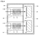
- FIG. 4 is a sectional view taken along line IV-IV of FIG.
- the uninterruptible power supply device 100 has a configuration in which components are housed inside a cabinet 102 (cuboid shape). Specifically, inside the housing 102, semiconductor units 1A to 1C and 2A to 2C, a capacitor unit 18, a circuit breaker unit 16, a control unit 14, and reactor units LA and LB are mounted. In addition to these units, elements and devices forming the electric circuit shown in FIG. 1 are mounted inside the housing 102, but they are omitted here.
- the inside of the housing 102 is divided into a space 104 in which most of the components are mounted and a space 106 that functions as a wind tunnel through which cooling air passes.
- the space 104 is arranged on the front side (left side of the paper) of the uninterruptible power supply 100, and the space 106 is arranged on the rear side (right side of the paper).
- the cooling fan 8 is provided on the upper surface (ceiling surface) of the housing 102.
- the space 104 and the space 106 are partitioned by a partition plate 110.
- the front surface of the housing 102 corresponds to one example of the “first surface”, and the upper surface of the housing 102 corresponds to one embodiment of the “second surface”.
- the space 104 corresponds to an example of the “first space”
- the space 106 corresponds to an example of the “second space”.
- the semiconductor units 1A to 1C and 2A to 2C all have substantially the same shape.
- the semiconductor unit has a rectangular parallelepiped shape.
- the semiconductor units 1A to 1C and 2A to 2C are arranged below the space 104.
- the semiconductor units 2A to 2C are arranged adjacent to the semiconductor units 1A to 1C in the horizontal direction (corresponding to the depth direction in the drawing).
- the switching element 10 in each semiconductor unit has a thin plate shape.
- the switching element 10 is arranged on the cooling fin 12.
- the cooling fins 12 are mounted on the back side of each semiconductor unit.
- Each semiconductor unit has a structure in which cooling air passes from the front surface side to the back surface side.
- the arrows in the figure indicate the flow of cooling air.
- the switching element 10 is cooled by cooling the cooling fins 12 with the cooling air.
- each semiconductor unit is close to the front surface of the housing 102, and the back surface of each semiconductor unit is close to the partition plate 110.
- the semiconductor units 1A to 1C are arranged in the vertical direction, and there is a gap between the semiconductor units.
- the semiconductor unit 1C is installed on the bottom surface of the housing 102.
- the semiconductor unit 1B is installed on the semiconductor unit 1C.
- the semiconductor unit 1A is installed on the semiconductor unit 1B.
- the capacitor unit 18 is a unit that houses the capacitors C1 to C6 shown in FIG.
- the control unit 14 is a unit on which a board or the like constituting the control device 4 shown in FIG. 1 is mounted.
- the circuit breaker unit 16 is a unit that houses the switches S1 to S6 shown in FIG.
- the capacitor unit 18, the circuit breaker unit 16, and the control unit 14 are installed above the semiconductor unit 1A in the space 104.
- the case 102 is formed with cooling air intake ports 112A and 112B.
- the intake port 112A is formed in the lower portion of the front surface of the housing 102 at a position where the semiconductor units 1A to 1C are located.
- the intake port 112B is formed in the lower portion of the front surface of the housing 102 at a position where the semiconductor units 2A to 2C are located.
- the partition plate 110 is formed with six openings 114A, 116A, 118A, 114B, 116B, 118B.
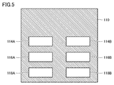
- FIG. 5 is an external view of the partition plate 110. Each opening is arranged corresponding to the portion located on the back surface of each semiconductor unit.
- the opening 114A is arranged in a portion located on the back surface of the semiconductor unit 1A
- the opening 116A is arranged in a portion located on the back surface of the semiconductor unit 1B
- a portion located on the back surface of the semiconductor unit 1C The opening 118A is arranged.
- an opening 114B is arranged in a portion located on the back surface of the semiconductor unit 2A
- an opening 116B is arranged in a portion located on the back surface of the semiconductor unit 2B
- a portion located on the back surface of the semiconductor unit 2C is arranged.
- the cooling air taken in from the intake port 112A passes through so as to cool the cooling fins 12 of the semiconductor units 1A to 1C, and the openings 114A, 116A, 118A of the partition plate 110. Is discharged to the space 106.
- the cooling air discharged into the space 106 flows upward and is discharged from the cooling fan 8 to the outside of the housing 102.
- the reactor unit LA is a unit that houses the reactors L1 to L3 shown in FIG.
- Reactor unit LB is a unit that houses reactors L4 to L6 shown in FIG.
- Each of reactors L1 to L6 has a coil and a terminal provided at an end of a conductor extending from the coil.
- Each of the reactor units LA and LB has, for example, a rectangular parallelepiped shape or a columnar shape.
- Reactor units LA and LB are installed in space 106. That is, the reactor units LA and LB are arranged in the wind tunnel of the cooling air that has cooled the semiconductor units 1A to 1C and 2A to 2C.
- the reactor unit LA is arranged so as to face at least one of the openings 114A, 116A, 118A of the partition plate 110.
- the reactor unit LB is arranged so as to face at least one of the openings 114B, 116B, 118B of the partition plate 110.
- the reactor unit LA is arranged so as to face the opening 114A.
- the reactor unit LB is arranged so as to face the opening 114B.
- the cooling air discharged from the opening 114A can be directly applied to the reactor unit LA.
- the cooling air discharged from the opening 114B can be directly applied to the reactor unit LB.
- the current density of the reactor is reduced by forming a coil using a winding wire with a large wire diameter. There is. Alternatively, the number of turns of the reactor is increased in order to increase the heat radiation area. However, it is feared that these measures will lead to increase in size and weight of the reactor and increase in cost. In order to reduce the size, weight and cost of the reactor, it is necessary to improve the heat dissipation of the reactor.
- the heat dissipation of the reactor can be improved by directly applying cooling air to the reactor units LA and LB. As a result, it is possible to prevent the reactor from increasing in size and weight and from increasing costs.
- the reactor units LA and LB are arranged so that the respective terminal portions 20 face the openings 116A and 116B, respectively.
- the terminal portion 20 is composed of a terminal provided at an end portion of a conductor wire extending from a coil of a reactor housed in each reactor unit, and projects to the outside of the reactor unit. Therefore, the heat generated in the reactor can be transferred from the terminal portion 20 to the outside. That is, the terminal portion 20 can function as a heat dissipation member of the reactor. By directly applying the cooling air to the terminal portion 20, the heat dissipation of the reactor can be improved.
- the heat radiation of the reactor can be improved by directly applying the cooling air of the semiconductor unit to the reactor unit.
- the thermal design of the reactor is simplified, so that the reactor can be reduced in size and weight and reduced in cost.
- the reactor unit may be arranged so as to face the opening having the fastest cooling air speed.
- FIG. 6 is a side sectional view of the uninterruptible power supply device 100 according to the first modification of the embodiment of the present invention.
- the opening 116A among the openings 114A, 116A, and 118A has the fastest cooling air velocity. Therefore, the reactor unit LA is arranged so as to face the opening 116A.
- the cooling fan 8 when there are variations in the cooling air velocity, in order to cool all the semiconductor units 1A to 1C sufficiently, the cooling fan 8 is set so that the semiconductor unit with the slowest air velocity is sufficiently cooled. Selected. Therefore, the cooling air having a wind speed faster than necessary flows to the semiconductor unit 1B having the highest wind speed. That is, the cooling fan 8 consumes extra energy.
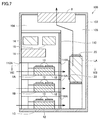
- FIG. 7 is a side sectional view of uninterruptible power supply 100 according to a second modification of the embodiment of the present invention.
- FIG. 8 is a cross-sectional view taken along the line VIII-VIII of FIG. 7.
- a radiator plate 22 is joined to the side surface of the reactor unit LA on the opening side.
- the heat dissipation plate 22 has, for example, a rectangular planar shape.
- the heat dissipation plate 22 may have cooling fins.
- the heat dissipation plate 22 may be thermally connected to the reactor unit LA. The heat generated from the reactor is radiated to the outside of the reactor unit LA via the heat dissipation plate 22.
- the reactor units LA and LB are arranged so that the heat dissipation plate 22 faces the opening.
- the reactor unit LA is arranged so that the heat dissipation plate 22 faces the opening 114A
- the reactor unit LB is arranged so that the heat dissipation plate 22 faces the opening 114B. ..
- the cooling air can be applied to the heat dissipation plate 22 in series, so that the heat dissipation of the reactor can be improved.
- the configuration for cooling the reactor unit in which the reactor is mounted with the cooling air has been described.
- the present embodiment and the modification examples are also applied to the transformer.
- the heat dissipation of the transformer can be improved.
- the cooling of reactor units LA and LB was mainly described, but the configuration described in the embodiment is also applied to other components such as a control unit, a capacitor unit, and a circuit breaker unit. Therefore, heat dissipation can be improved.
- the configuration of the semiconductor units stacked in three stages has been described, but the semiconductor units do not necessarily have to be stacked in multiple stages. Also, any number of openings may be provided. By disposing the reactor unit so as to face the opening provided corresponding to the semiconductor unit, heat dissipation of the reactor can be enhanced.
Landscapes
- Engineering & Computer Science (AREA)
- Microelectronics & Electronic Packaging (AREA)
- Physics & Mathematics (AREA)
- Thermal Sciences (AREA)
- Power Engineering (AREA)
- Inverter Devices (AREA)
- Cooling Or The Like Of Electrical Apparatus (AREA)
- Dc-Dc Converters (AREA)
Abstract
盤形状の筐体(102)は、吸気口(112A)が形成された第1の面と、第1の面とは異なる第2の面とを有する。冷却ファン(8)は第2の面に設けられ、第2の面から排気する。仕切り板(110)は、筐体(102)の内部の空間を、第1の面に接する第1の空間(104)と、第2の面に接する第2の空間(106)とに仕切るように構成される。仕切り板(110)には、冷却ファン(8)により発生する冷却風が第1の空間(104)から第2の空間(106)に通り抜ける少なくとも1つの開口部(114A,116A,118A)が形成されている。少なくとも1つの半導体ユニット(1A,1B,1C)は、第1の空間(104)に配置され、冷却風により冷却される。リアクトルユニット(LA)は、少なくとも1つの開口部に対向するように第2の空間(106)に配置される。
Description
本発明は、半導体装置に関する。
特開2016-19324号公報(特許文献1)には、半導体ユニットと、半導体ユニットを強制風冷により冷却する冷却構造とを備える半導体装置が開示される。特許文献1では、盤形状の筐体の内部に複数の半導体ユニットを垂直方向に配置し、冷却ファンにより上部から冷却風を排気する。
上記特許文献1に記載される半導体装置において、筐体の内部の空間には半導体ユニット以外にリアクトルが実装されている。リアクトルは、半導体ユニットと同様に発熱する部品であるため、冷却が必要となる。
リアクトルの熱設計では、一般的に、リアクトルの単位体積当たりの発熱量を抑えるために、線径の太い巻線を使用してリアクトルの電流密度を下げることが行なわれている。または、放熱面積を稼ぐために、リアクトルの巻き数を増やすことが行なわれている。しかしながら、これらの対策はリアクトルの大型化および重量化に繋がるとともに、コストの上昇を招くことが懸念される。
この発明は、上記のような課題を解決するためになされたものであり、装置を大型化および重量化することなく、リアクトルの放熱性を向上させることが可能な半導体装置を提供することである。
この発明のある局面によれば、半導体装置は、吸気口が形成された第1の面と第1の面とは異なる第2の面とを有する盤形状の筐体と、第2の面に設けられ、第2の面から排気する冷却ファンと、筐体の内部の空間を、第1の面に接する第1の空間と、第2の面に接する第2の空間とに仕切るように構成された仕切り板とを備える。仕切り板には、冷却ファンにより発生する冷却風が第1の空間から第2の空間に通り抜ける少なくとも1つの開口部が形成されている。半導体装置は、さらに、第1の空間に配置され、冷却風により冷却される少なくとも1つの半導体ユニットと、少なくとも1つの開口部に対向するように第2の空間に配置されるリアクトルユニットとを備える。
本発明によれば、装置を大型化および重量化することなく、リアクトルの放熱性を向上させることができる半導体装置を提供することができる。
以下、本発明の実施の形態について図面を参照して詳細に説明する。なお、以下では図中の同一または相当部分には同一符号を付してその説明は原則的に繰返さないものとする。
図1は、本発明の実施の形態に係る半導体装置が適用され得る無停電電源装置の構成を示す回路ブロック図である。図1を参照して、無停電電源装置100は、交流入力端子5a~5c、コンデンサC1~C6、リアクトルL1~L6、コンバータ1、直流ラインPL,NL、インバータ2、交流出力端子6a~6c、および制御装置4を備える。無停電電源装置100は、商用交流電源5から商用周波数の三相交流電力を受け、負荷6に商用周波数の三相交流電力を供給する。
商用交流電源5は、三相3線式であり、交流入力端子5a~5cに三相交流電圧を出力する。負荷6は、三相3線式であり、交流出力端子6a~6cに接続される。
コンデンサC1~C3の一方電極は交流入力端子5a~5cにそれぞれ接続され、それらの他方電極はともにノードNPに接続される。リアクトルL1~L3の一方端子は交流入力端子5a~5cにそれぞれ接続され、それらの他方端子はコンバータ1の入力ノードにそれぞれ接続される。
コンデンサC1~C3およびリアクトルL1~L3は、低域通過フィルタを構成し、商用交流電源5からコンバータ1に商用周波数の交流電流を流し、コンバータ1から商用交流電源5にスイッチング周波数の信号が流れることを防止する。
商用交流電源5からの三相交流電圧(交流入力電圧)の瞬時値は、制御装置4によって検出される。図示しない電流検出器は、リアクトルL1~L3に流れる交流電流(交流入力電流)を検出し、検出値を示す信号を制御装置4に与える。
コンバータ1の正側出力ノードは、直流ラインPLを介してインバータ2の正側入力ノードに接続される。コンバータ1の負側出力ノードは、直流ラインNLを介してインバータ2の負側入力ノードに接続される。
直流ラインPL,NL間に、バッテリ7(電力貯蔵装置)が接続される。バッテリ7は、直流電力を蓄える。バッテリ7の代わりにコンデンサが接続されていても構わない。直流ラインPL,NL間の直流電圧は、制御装置4によって検出される。
コンバータ1は、制御装置4によって制御され、商用交流電源5から三相交流電力が正常に供給されている健全時には、商用交流電源5からの三相交流電力を直流電力に変換する。コンバータ1によって生成された直流電力は、直流ラインPL,NLを介してインバータ2に供給されるとともに、バッテリ7に蓄えられる。
このときコンバータ1は、直流ラインPL,NL間の直流電圧が所定の参照直流電圧になるように、電流を出力する。これにより、直流電圧は一定に保たれる。商用交流電源5からの三相交流電力の供給が停止された停電時には、コンバータ1の運転は停止される。
インバータ2は、制御装置4によって制御され、商用交流電源5から三相交流電力が正常に供給されている健全時には、コンバータ1からの直流電力を商用周波数の三相交流電力に変換する。また、インバータ2は、商用交流電源5からの三相交流電力の供給が停止された停電時には、バッテリ7の直流電力を商用周波数の三相交流電力に変換する。
インバータ2の3つの出力ノードは、リアクトルL4~L6の一方端子にそれぞれ接続される。リアクトルL4~L6の他方端子はスイッチS1~S3の一方端子にそれぞれ接続され、スイッチS1~S3の他方端子は交流出力端子6a~6cにそれぞれ接続される。コンデンサC4~C6の一方電極はリアクトルL4~L6の他方端子にそれぞれ接続され、コンデンサC4~C6の他方電極はともにノードNPに接続される。
コンデンサC4~C6およびリアクトルL4~L6は、低域通過フィルタを構成し、インバータ2から負荷6に商用周波数の交流電流を流し、インバータ2から負荷6にスイッチング周波数の信号が流れることを防止する。換言すると、コンデンサC4~C6およびリアクトルL4~L6は、インバータ2から出力される三相矩形波電圧を正弦波状の三相交流電圧(交流出力電圧)に変換する。
交流出力電圧の瞬時値は、制御装置4によって検出される。図示しない電流検出器は、リアクトルL4~L6に流れる交流電流(交流出力電流)を検出し、検出値を示す信号を制御装置4に与える。
スイッチS4~S6の一方端子は交流入力端子5a~5cにそれぞれ接続され、それらの他方端子は交流出力端子6a~6cにそれぞれ接続される。スイッチS1~S6は、制御装置4によって制御される。
インバータ2によって生成される三相交流電力を負荷6に供給するインバータ給電モード時には、スイッチS1~S3がオンされるとともに、スイッチS4~S6がオフされる。商用交流電源5からの三相交流電力を負荷6に供給するバイパス給電モード時には、スイッチS1~S3がオフされるとともに、スイッチS4~S6がオンされる。
制御装置4は、交流入力電圧、交流入力電流、直流電圧、交流出力電流、および交流出力電圧などに基づいて無停電電源装置100全体を制御する。すなわち、制御装置4は、交流入力電圧の検出値に基づいて停電が発生したか否かを検出する。
制御装置4は、商用交流電源5から三相交流電力が供給されている健全時は、インバータ給電モードを選択し、スイッチS1~S3をオンさせるとともに、スイッチS4~S6をオフさせる。これにより、コンバータ1で生成された直流電力がインバータ2によって三相交流電力に変換され、その三相交流電力がスイッチS1~S3を介して負荷6に供給される。
制御装置4は、商用交流電源5からの三相交流電力の供給が停止された停電時は、コンバータ1の運転を停止させる。これにより、バッテリ7の直流電力がインバータ2によって三相交流電力に変換され、その三相交流電力がスイッチS1~S3を介して負荷6に供給される。バッテリ7の端子間電圧が放電終止電圧に低下した場合は、制御装置4は、さらにインバータ2の運転を停止させ、スイッチS1~S3をオフさせる。
商用交流電源5の健全時においてインバータ2が故障した場合には、制御装置4は、バイパス給電モードを選択し、スイッチS4~S6をオン状態に維持しながら、スイッチS1~S3をオフさせる。これにより、商用交流電源5から負荷6に三相交流電力が供給される。
図2は、図1に示したコンバータ1およびインバータ2の構成を示す回路図である。図2では、スイッチS1~S6および制御装置4の図示は省略されている。
図2を参照して、コンバータ1は、IGBT(Insulated Gate Bipolar Transistor)Q1~Q6、ダイオードD1~D6、コンデンサC1A~C1C、およびヒューズF1~F6を含む。図2では、電力用半導体スイッチング素子(以下、単に「スイッチング素子」とも称する)としてIGBTを用いているが、MOSFET(Metal Oxide Semiconductor Field Effect Transistor)などの任意の自己消弧型のスイッチング素子を用いることができる。
IGBTQ1~Q3のコレクタはともに直流ラインPLに接続され、それらのエミッタはそれぞれリアクトルL1~L3の他方端子に接続される。IGBTQ4~Q6のコレクタはそれぞれリアクトルL1~L3の他方端子に接続され、それらのエミッタはともに直流ラインNLに接続される。
ダイオードD1~D6の各々は、対応するスイッチング素子のオフ時にフリーホイール電流を流すために設けられている。スイッチング素子がMOSFETである場合、フリーホイールダイオードは寄生のダイオード(ボディダイオード)で構成される。スイッチング素子がダイオードを内蔵しないIGBTである場合、フリーホイールダイオードはIGBTに逆並列に接続されたダイオードで構成される。
ヒューズF1,F3,F5は、IGBTQ1,Q3,Q5のコレクタと直流ラインPLとの間にそれぞれ接続される。ヒューズF2,F4,F6は、IGBTQ2,Q4,Q6のエミッタと直流ラインNLとの間にそれぞれ接続される。
コンデンサC1Aは、IGBTQ1のコレクタとIGBTQ2のエミッタとの間に接続される。コンデンサC1Bは、IGBTQ3のコレクタとIGBTQ4のエミッタとの間に接続される。コンデンサC1Cは、IGBTQ5のコレクタとIGBTQ6のエミッタとの間に接続される。コンデンサC1A~C1Cの各々は、直流ラインPLおよびNL間に入力された直流電圧を平滑化する。
IGBTQ1,Q4はそれぞれゲート信号Au,Buによって制御され、IGBTQ2,Q5はそれぞれゲート信号Av,Bvによって制御され、IGBTQ3,Q6はそれぞれゲート信号Aw,Bwによって制御される。ゲート信号Bu,Bv,Bwは、それぞれゲート信号Au,Av,Awの反転信号である。ゲート信号Au,Bu,Av,Bv,Aw,Bwの各々は、パルス信号列であり、PWM(Pulse Width Modulation)信号である。ゲート信号Au,Buの位相とゲート信号Av,Bvの位相とゲート信号Aw,Bwの位相とは120度ずつずれている。ゲート信号Au,Bu,Av,Bv,Aw,Bwは、制御装置4によって生成される。ゲート信号Au,Bu,Av,Bv,Aw,BwによってIGBTQ1~Q6の各々を所定のタイミングでオンおよびオフさせるとともに、IGBTQ1~Q6の各々のオン時間を調整することにより、交流入力端子5a~5cに与えられた三相交流電圧を直流電圧に変換することが可能となっている。
インバータ2は、IGBTQ11~Q16、ダイオードD11~D16、コンデンサC2A~C2C、およびヒューズF11~F16を含む。IGBTQ11,Q13,Q15のコレクタはともに直流ラインPLに接続され、それらのエミッタはそれぞれリアクトルL4~L6の一方端子に接続される。IGBTQ12,Q14,Q16のコレクタはそれぞれリアクトルL4~L6の一方端子に接続され、それらのエミッタはともに直流ラインNLに接続される。ダイオードD11~D16の各々は、対応するスイッチング素子のオフ時にフリーホイール電流を流すために設けられている。
IGBTQ11,Q12はそれぞれゲート信号Xu,Yuによって制御され、IGBTQ13,Q14はそれぞれゲート信号Xv,Yvによって制御され、IGBTQ15,Q16はそれぞれゲート信号Xw,Ywによって制御される。ゲート信号Yu,Yv,Ywは、それぞれゲート信号Xu,Xv,Xwの反転信号である。ゲート信号Xu,Yu,Xv,Yv,Xw,Ywの各々は、パルス信号列であり、PWM信号である。ゲート信号Xu,Yuの位相とゲート信号Xv,Yvの位相とゲート信号Xw,Ywの位相とは120度ずつずれている。ゲート信号Xu,Yu,Xv,Yv,Xw,Ywは、制御装置4によって生成される。ゲート信号Xu,Yu,Xv,Yv,Xw,YwによってIGBTQ11~Q16の各々を所定のタイミングでオンおよびオフさせるとともに、IGBTQ11~Q16の各々のオン時間を調整することにより、直流ラインPL,NL間の直流電圧を三相交流電圧に変換することが可能となっている。
図2に示した構成において、IGBTQ1,Q2、ダイオードD1,D2、ヒューズF1,F2およびコンデンサC1Aは、1つの半導体ユニット1Aで構成されている。IGBTQ3,Q4、ダイオードD3,D4、ヒューズF3,F4およびコンデンサC1Bは、半導体ユニット1Bで構成されている。IGBTQ5,Q6、ダイオードD5,D6、ヒューズF5,F6およびコンデンサC1Cは、半導体ユニット1Cで構成されている。
IGBTQ11,Q12、ダイオードD11,D12、ヒューズF11,F12およびコンデンサC2Aは、半導体ユニット2Aで構成されている。IGBTQ13,Q14、ダイオードD13,D14、ヒューズF13,F14およびコンデンサC2Bは、半導体ユニット2Bで構成されている。IGBTQ15,Q16、ダイオードD15,D16、ヒューズF15,F16およびコンデンサC2Cは、半導体ユニット2Cで構成されている。
半導体ユニット1A~1C,2A~2Cの各々は、平面状の基板上に、IGBTおよびダイオードからなるスイッチング素子が2つ実装された構成を有している。IGBTおよびダイオードは、ボンディングワイヤまたは導電体からなる配線層によって電気的に接続されている。IGBTおよびダイオードは、基板および配線層などとともに樹脂により封止されている。コンデンサは基板に隣接して設置される。
半導体ユニット1A~1C,2A~2Cの各々は、その動作中にスイッチング素子に導通損失およびスイッチング損失からなる電力損失が発生する。その電力損失によりスイッチング素子が発熱する。
図1に示すように、無停電電源装置100は、半導体ユニット1A~1C,2A~2Cを冷却するための構成として、冷却ファン8を備える。冷却ファン8は、インバータ2から三相交流電力の供給を受けて駆動する。冷却ファン8による強制風冷により半導体ユニット1A~1C,2A~2Cを冷却する。
次に、図3を参照して、無停電電源装置100の構成について説明する。
図3は、無停電電源装置100の側方断面図である。図4は、図3のIV-IV線に沿った断面図である。
図3は、無停電電源装置100の側方断面図である。図4は、図3のIV-IV線に沿った断面図である。
図3に示すように、無停電電源装置100は、盤形状(直方体形状)の筐体102の内部に構成部品が収納された構成を有している。具体的には、筐体102の内部には、半導体ユニット1A~1C,2A~2C、コンデンサユニット18、遮断器ユニット16、制御ユニット14、およびリアクトルユニットLA,LBが実装されている。なお、筐体102の内部には、これらのユニットの他にも図1に示した電気回路を構成する素子および機器などが実装されているが、ここでは省略する。
筐体102の内部は、大半の構成部品が実装された空間104と、冷却風が通り抜ける風洞としての役割を持つ空間106とに分けられている。空間104は無停電電源装置100の前面側(紙面左側)に配置され、空間106は背面側(紙面右側)に配置されている。筐体102の上面(天井面)には冷却ファン8が設けられている。空間104と空間106とは仕切り板110によって仕切られている。筐体102の前面は「第1の面」の一実施例に対応し、筐体102の上面は「第2の面」の一実施例に対応する。空間104は「第1の空間」の一実施例に対応し、空間106は「第2の空間」の一実施例に対応する。
半導体ユニット1A~1C,2A~2Cは全てほぼ同じ形状を有している。図3の例では、半導体ユニットは直方体形状を有している。半導体ユニット1A~1C,2A~2Cは空間104の下側に配置されている。図3では示されていないが、半導体ユニット2A~2Cは、半導体ユニット1A~1Cと水平方向(紙面奥行方向に相当)に隣接して配置されている。
各半導体ユニットにおいて、スイッチング素子10は薄板形状を有する。スイッチング素子10は、冷却フィン12上に配置されている。冷却フィン12は、各半導体ユニットの背面側に実装されている。各半導体ユニットは、前面側から背面側に冷却風が通り抜ける構造である。図中の矢印は冷却風の流れを示している。冷却フィン12が冷却風により冷却されることで、スイッチング素子10が冷却される。
各半導体ユニットの前面は筐体102の前面に近接し、各半導体ユニットの背面は仕切り板110に近接している。半導体ユニット1A~1Cは、垂直方向に配置されており、各半導体ユニットの間には隙間がある。図3の例では、半導体ユニット1Cは、筐体102の底面に設置されている。半導体ユニット1Bは、半導体ユニット1Cの上に設置されている。半導体ユニット1Aは、半導体ユニット1Bの上に設置されている。
コンデンサユニット18は、図1に示したコンデンサC1~C6が収納されたユニットである。制御ユニット14は、図1に示した制御装置4を構成する基板等が実装されたユニットである。遮断器ユニット16は、図1に示したスイッチS1~S6が収納されたユニットである。コンデンサユニット18、遮断器ユニット16および制御ユニット14は、空間104の半導体ユニット1Aの上方に設置されている。
筐体102には、冷却風の吸気口112A,112Bが形成されている。吸気口112Aは、筐体102の前面の下部に、半導体ユニット1A~1Cが位置する箇所に形成されている。吸気口112Bは、筐体102の前面の下部に、半導体ユニット2A~2Cが位置する箇所に形成されている。
仕切り板110には、6つの開口部114A,116A,118A,114B,116B,118Bが形成されている。図5は、仕切り板110の外形図である。各開口部は、各半導体ユニットの背面に位置する部分に対応して配置されている。図3の例では、半導体ユニット1Aの背面に位置する部分に開口部114Aが配置され、半導体ユニット1Bの背面に位置する部分に開口部116Aが配置され、半導体ユニット1Cの背面に位置する部分に開口部118Aが配置されている。図示は省略するが、半導体ユニット2Aの背面に位置する部分に開口部114Bが配置され、半導体ユニット2Bの背面に位置する部分に開口部116Bが配置され、半導体ユニット2Cの背面に位置する部分に開口部118Bが配置されている。
図3および図4に矢印で示すように、吸気口112Aから取り込まれた冷却風は、半導体ユニット1A~1Cの冷却フィン12を冷却するように通り抜け、仕切り板110の開口部114A,116A,118Aから空間106に排出される。空間106に排出された冷却風は上向きに流れ、冷却ファン8から筐体102の外部へ排出される。
リアクトルユニットLAは、図1に示したリアクトルL1~L3が収納されたユニットである。リアクトルユニットLBは、図1に示したリアクトルL4~L6が収納されたユニットである。リアクトルL1~L6の各々は、コイルと、当該コイルから延びる導線の端部に設けられた端子とを有する。
リアクトルユニットLA,LBの各々は、例えば直方体形状または円柱形状を有している。リアクトルユニットLA,LBは空間106に設置されている。すなわち、リアクトルユニットLA,LBは、半導体ユニット1A~1C,2A~2Cを冷却した冷却風の風洞に配置される。
具体的には、図4に示すように、リアクトルユニットLAは、仕切り板110の開口部114A,116A,118Aの少なくとも1つに対向するように配置される。リアクトルユニットLBは、仕切り板110の開口部114B,116B,118Bの少なくとも1つに対向するように配置される。図3の例では、リアクトルユニットLAは、開口部114Aに対向するように配置されている。リアクトルユニットLBは、開口部114Bに対向するように配置されている。
このような構成とすることにより、開口部114Aから排出された冷却風をリアクトルユニットLAに直接的に当てることができる。同様に、開口部114Bから排出された冷却風をリアクトルユニットLBに直接的に当てることができる。
リアクトルの熱設計では、一般的に、リアクトルの単位体積当たりの発熱量を抑えるために、線径の太い巻線を使用してコイルを形成することでリアクトルの電流密度を下げることが行なわれている。または、放熱面積を稼ぐために、リアクトルの巻き数を増やすことが行なわれている。しかしながら、これらの対策はリアクトルの大型化および重量化に繋がるとともに、コストの上昇を招くことが懸念される。リアクトルの小型軽量化および低コスト化のためには、リアクトルの放熱性を向上させることが求められる。
本実施の形態では、リアクトルユニットLA,LBに直接的に冷却風を当てることにより、リアクトルの放熱性を高めることができる。これにより、リアクトルの大型化および重量化ならびにコスト上昇を抑制することができる。
なお、図3および図4の例では、リアクトルユニットLA,LBを、各々の端子部20が開口部116A,116Bにそれぞれ対向するように配置している。端子部20は、各リアクトルユニットに収納されるリアクトルのコイルから延びる導線の端部に設けられる端子で構成されており、リアクトルユニットの外部に突き出している。したがって、リアクトルで発生した熱を端子部20から外部へ伝えることができる。すなわち、端子部20はリアクトルの放熱部材として機能し得る。この端子部20に直接的に冷却風を当てることにより、リアクトルの放熱性を高めることができる。
以上説明したように、本実施の形態に係る半導体装置によれば、半導体ユニットの冷却風をリアクトルユニットに直接的に当てることにより、リアクトルの放熱性を向上させることができる。これにより、リアクトルの熱設計が簡易化されるため、リアクトルを小型軽量化および低コスト化を実現することができる。
<変形例1>
上述した実施の形態では、リアクトルユニットLAを、3つの開口部114A,116A,118Aのうち少なくとも1つに対向するように配置する構成について説明した。
上述した実施の形態では、リアクトルユニットLAを、3つの開口部114A,116A,118Aのうち少なくとも1つに対向するように配置する構成について説明した。
ただし、開口部114A,116A,118Aから排出される冷却風の風速にばらつきが存在する場合には、冷却風の風速が最も速い開口部に対向するようにリアクトルユニットを配置する構成としてもよい。
図6は、本発明の実施の形態の第1の変形例に係る無停電電源装置100の側方断面図である。図6では、開口部114A,116A,118Aのうち開口部116Aが冷却風の風速が最も速い場合を想定している。したがって、開口部116Aに対向するようにリアクトルユニットLAを配置している。
図6のように、冷却風の風速にばらつきがある場合、全ての半導体ユニット1A~1Cを十分に冷却するためには、最も風速が遅い半導体ユニットが十分に冷却されるように冷却ファン8が選定される。そのため、最も風速が速い半導体ユニット1Bに対しては、必要以上に速い風速の冷却風が流れることになる。すなわち、冷却ファン8は余分なエネルギーを消費していることになる。
図6の例では、最も風速が速い冷却風をリアクトルユニットLAに当てることにより、余分なエネルギーをリアクトルの冷却に活用することができる。これによると、リアクトルを冷却するためのエネルギー消費を抑えることができるため、半導体ユニットおよびリアクトルを効率良く冷却することができる。
<変形例2>
上述した実施の形態では、リアクトルユニットLA,LBの端子部20に冷却風を当てる構成について説明した。しかしながら、筐体102内部のレイアウトおよびリアクトルユニットの形状によっては、仕切り板110の開口部に端子部20が対向するようにリアクトルユニットを配置することが困難となる場合がある。このような場合には、リアクトルユニットLA,LBに放熱板(ヒートシンク)を接合し、放熱板に冷却風を当てる構成を採用してもよい。
上述した実施の形態では、リアクトルユニットLA,LBの端子部20に冷却風を当てる構成について説明した。しかしながら、筐体102内部のレイアウトおよびリアクトルユニットの形状によっては、仕切り板110の開口部に端子部20が対向するようにリアクトルユニットを配置することが困難となる場合がある。このような場合には、リアクトルユニットLA,LBに放熱板(ヒートシンク)を接合し、放熱板に冷却風を当てる構成を採用してもよい。
図7は、本発明の実施の形態の第2の変形例に係る無停電電源装置100の側方断面図である。図8は、図7のVIII-VIII線に沿った断面図である。
図7を参照して、リアクトルユニットLAの開口部側の側面には放熱板22が接合されている。放熱板22は、例えば矩形の平面形状を有している。放熱板22は、冷却フィンを有していてもよい。放熱板22は、リアクトルユニットLAと熱的に接続されていればよい。リアクトルからの発熱は、放熱板22を介してリアクトルユニットLAの外部に放出される。
リアクトルユニットLA,LBは、放熱板22が開口部に対向するように配置されている。図7および図8の例では、リアクトルユニットLAは、放熱板22が開口部114Aに対向するように配置され、リアクトルユニットLBは、放熱板22が開口部114Bに対向するように配置されている。これにより、放熱板22に直列的に冷却風を当てることができるため、リアクトルの放熱性を高めることができる。
なお、図示は省略するが、放熱板22をリアクトルユニットの端子部20と近接して配置することで、放熱板22および端子部20の双方に冷却風を直接的に当てることができる。したがって、リアクトルの放熱性をさらに高めることが可能となる。
上述した実施の形態では、リアクトルが実装されたリアクトルユニットを冷却風で冷却するための構成について説明したが、無停電電源装置がトランスを有する場合には、トランスについても本実施の形態および変更例で示した構成を適用することで、トランスの放熱性を向上させることができる。
また、本実施の形態では、リアクトルユニットLA,LBの冷却について主に説明したが、制御ユニット、コンデンサユニットおよび遮断器ユニットなどの他の構成部品についても、実施の形態で説明した構成を適用することで、放熱性を高めることができる。
また、本実施の形態では、三段積みの半導体ユニットの構成について説明したが、半導体ユニットは必ずしも多段積みでなくてもよい。また、開口部はいくつでもよい。半導体ユニットに対応して設けられた開口部に対向するようにリアクトルユニットを配置することで、リアクトルの放熱性を高めることができる。
今回開示された実施の形態はすべての点で例示であって制限的なものではないと考えられるべきである。本発明の範囲は上記した説明ではなくて請求の範囲によって示され、請求の範囲と均等の意味および範囲内でのすべての変更が含まれることが意図される。
1 コンバータ、2 インバータ、4 制御装置、5 商用交流電源、5a~5c 交流入力端子、6 負荷、6a~6c 交流出力端子、7 バッテリ、8 冷却ファン、10 スイッチング素子、12 冷却フィン、14 制御ユニット、16 遮断器ユニット、18 コンデンサユニット、20 端子部、22 放熱板、100 無停電電源装置、102 筐体、104,106 空間、110 仕切り板、112A,112B 吸気口、114A,114B,116A,116B,118A,118B 開口部、C1~C6,C1A~C1C,C2A~C2C コンデンサ、L1~L6 リアクトル、LA,LB リアクトルユニット、Q1~Q6,Q11~Q16 IGBT、D1~D6 ダイオード、F1~F6,F11~F16 ヒューズ,S1~S6 スイッチ。
Claims (5)
- 吸気口が形成された第1の面と、前記第1の面とは異なる第2の面とを有する盤形状の筐体と、
前記第2の面に設けられ、前記第2の面から排気する冷却ファンと、
前記筐体の内部の空間を、前記第1の面に接する第1の空間と、前記第2の面に接する第2の空間とに仕切るように構成された仕切り板とを備え、
前記仕切り板には、前記冷却ファンにより発生する冷却風が前記第1の空間から前記第2の空間に通り抜ける少なくとも1つの開口部が形成されており、
前記第1の空間に配置され、前記冷却風により冷却される少なくとも1つの半導体ユニットと、
前記少なくとも1つの開口部に対向するように前記第2の空間に配置され、リアクトルを収納するリアクトルユニットとをさらに備える、半導体装置。 - 前記少なくとも1つの開口部は、複数の開口部であり、
前記リアクトルユニットは、前記複数の開口部のうち冷却風の風速が最も速い開口部に対向するように配置される、請求項1に記載の半導体装置。 - 前記リアクトルユニットは、前記リアクトルの端子を含む端子部を有しており、
前記リアクトルユニットは、前記端子部が前記開口部に対向するように配置される、請求項1または2に記載の半導体装置。 - 前記リアクトルユニットに熱的に接続された放熱板をさらに備え、
前記リアクトルユニットは、前記放熱板が前記開口部に対向するように配置される、請求項1から3のいずれか1項に記載の半導体装置。 - 前記仕切り板において、前記少なくとも1つの開口部は、前記少なくとも1つの半導体ユニットにそれぞれ対応するように配置され、
前記リアクトルユニットは、前記少なくとも1つの開口部に対向するように配置される、請求項1から4のいずれか1項に記載の半導体装置。
Priority Applications (4)
| Application Number | Priority Date | Filing Date | Title |
|---|---|---|---|
| US16/959,881 US20200335423A1 (en) | 2018-11-27 | 2018-11-27 | Semiconductor device |
| JP2019531481A JPWO2020110202A1 (ja) | 2018-11-27 | 2018-11-27 | 半導体装置 |
| CN201880090328.3A CN111771328A (zh) | 2018-11-27 | 2018-11-27 | 半导体装置 |
| PCT/JP2018/043611 WO2020110202A1 (ja) | 2018-11-27 | 2018-11-27 | 半導体装置 |
Applications Claiming Priority (1)
| Application Number | Priority Date | Filing Date | Title |
|---|---|---|---|
| PCT/JP2018/043611 WO2020110202A1 (ja) | 2018-11-27 | 2018-11-27 | 半導体装置 |
Publications (1)
| Publication Number | Publication Date |
|---|---|
| WO2020110202A1 true WO2020110202A1 (ja) | 2020-06-04 |
Family
ID=70853960
Family Applications (1)
| Application Number | Title | Priority Date | Filing Date |
|---|---|---|---|
| PCT/JP2018/043611 Ceased WO2020110202A1 (ja) | 2018-11-27 | 2018-11-27 | 半導体装置 |
Country Status (4)
| Country | Link |
|---|---|
| US (1) | US20200335423A1 (ja) |
| JP (1) | JPWO2020110202A1 (ja) |
| CN (1) | CN111771328A (ja) |
| WO (1) | WO2020110202A1 (ja) |
Families Citing this family (2)
| Publication number | Priority date | Publication date | Assignee | Title |
|---|---|---|---|---|
| US11690195B2 (en) * | 2020-09-11 | 2023-06-27 | Abb Schweiz Ag | Power semiconductor cooling system |
| WO2023281601A1 (ja) * | 2021-07-05 | 2023-01-12 | 東芝三菱電機産業システム株式会社 | 電力変換装置 |
Citations (3)
| Publication number | Priority date | Publication date | Assignee | Title |
|---|---|---|---|---|
| JP2014150171A (ja) * | 2013-02-01 | 2014-08-21 | Sumitomo Electric Ind Ltd | リアクトル、コンバータ、および電力変換装置 |
| JP2016019324A (ja) * | 2014-07-07 | 2016-02-01 | 東芝三菱電機産業システム株式会社 | 半導体装置 |
| WO2016157411A1 (ja) * | 2015-03-31 | 2016-10-06 | 三菱電機株式会社 | リアクトル機構 |
Family Cites Families (3)
| Publication number | Priority date | Publication date | Assignee | Title |
|---|---|---|---|---|
| CN202158706U (zh) * | 2010-04-26 | 2012-03-07 | 株式会社东芝 | 冰箱 |
| JP6191660B2 (ja) * | 2014-08-05 | 2017-09-06 | 株式会社豊田中央研究所 | 熱伝導体、熱伝導体を備える半導体装置 |
| JP6217679B2 (ja) * | 2015-03-25 | 2017-10-25 | コニカミノルタ株式会社 | 電気機器用オプション装置 |
-
2018
- 2018-11-27 US US16/959,881 patent/US20200335423A1/en not_active Abandoned
- 2018-11-27 JP JP2019531481A patent/JPWO2020110202A1/ja active Pending
- 2018-11-27 WO PCT/JP2018/043611 patent/WO2020110202A1/ja not_active Ceased
- 2018-11-27 CN CN201880090328.3A patent/CN111771328A/zh active Pending
Patent Citations (3)
| Publication number | Priority date | Publication date | Assignee | Title |
|---|---|---|---|---|
| JP2014150171A (ja) * | 2013-02-01 | 2014-08-21 | Sumitomo Electric Ind Ltd | リアクトル、コンバータ、および電力変換装置 |
| JP2016019324A (ja) * | 2014-07-07 | 2016-02-01 | 東芝三菱電機産業システム株式会社 | 半導体装置 |
| WO2016157411A1 (ja) * | 2015-03-31 | 2016-10-06 | 三菱電機株式会社 | リアクトル機構 |
Also Published As
| Publication number | Publication date |
|---|---|
| CN111771328A (zh) | 2020-10-13 |
| JPWO2020110202A1 (ja) | 2021-02-15 |
| US20200335423A1 (en) | 2020-10-22 |
Similar Documents
| Publication | Publication Date | Title |
|---|---|---|
| CN101681898B (zh) | 半导体元件的冷却构造 | |
| JP4305537B2 (ja) | 電力変換装置 | |
| JP6296888B2 (ja) | 電力変換装置 | |
| US9099933B2 (en) | AC-to-AC converter and method for converting a first frequency AC-voltage to a second frequency AC-voltage | |
| CN113632364B (zh) | 电力变换单元 | |
| JP6471659B2 (ja) | インバータ制御基板 | |
| US10306814B2 (en) | Heat dissipation in power electronic assemblies | |
| US20170117820A1 (en) | Semiconductor device | |
| JP2018195694A (ja) | 電力変換器 | |
| WO2020110202A1 (ja) | 半導体装置 | |
| JP6974291B2 (ja) | 半導体装置 | |
| JP6761908B2 (ja) | 電力変換装置 | |
| JP6970045B2 (ja) | 電力変換装置 | |
| JP6984002B2 (ja) | 抵抗装置およびインバータ装置 | |
| JP7622907B2 (ja) | 電力変換装置 | |
| JPWO2021074981A1 (ja) | Dc/dcコンバータ装置 | |
| JP2021061692A (ja) | 電力変換装置 | |
| JP2024101333A (ja) | 電力変換装置 | |
| US20180006573A1 (en) | Electrical Power Conversion Unit and Electrical Power Conversion Device | |
| WO2025154342A1 (ja) | 電力変換装置 | |
| JP2024101332A (ja) | 電力変換装置 | |
| WO2018173154A1 (ja) | 電力変換ユニット | |
| JP2016040981A (ja) | 電力変換装置および電動車両 |
Legal Events
| Date | Code | Title | Description |
|---|---|---|---|
| ENP | Entry into the national phase |
Ref document number: 2019531481 Country of ref document: JP Kind code of ref document: A |
|
| 121 | Ep: the epo has been informed by wipo that ep was designated in this application |
Ref document number: 18941547 Country of ref document: EP Kind code of ref document: A1 |
|
| NENP | Non-entry into the national phase |
Ref country code: DE |
|
| 122 | Ep: pct application non-entry in european phase |
Ref document number: 18941547 Country of ref document: EP Kind code of ref document: A1 |