WO2020090482A1 - 周波数選択板設計装置 - Google Patents
周波数選択板設計装置 Download PDFInfo
- Publication number
- WO2020090482A1 WO2020090482A1 PCT/JP2019/040738 JP2019040738W WO2020090482A1 WO 2020090482 A1 WO2020090482 A1 WO 2020090482A1 JP 2019040738 W JP2019040738 W JP 2019040738W WO 2020090482 A1 WO2020090482 A1 WO 2020090482A1
- Authority
- WO
- WIPO (PCT)
- Prior art keywords
- resonance frequency
- capacitance
- inductance
- correction
- frequency
- Prior art date
- Legal status (The legal status is an assumption and is not a legal conclusion. Google has not performed a legal analysis and makes no representation as to the accuracy of the status listed.)
- Ceased
Links
Images



Classifications
-
- H—ELECTRICITY
- H01—ELECTRIC ELEMENTS
- H01Q—ANTENNAS, i.e. RADIO AERIALS
- H01Q15/00—Devices for reflection, refraction, diffraction or polarisation of waves radiated from an antenna, e.g. quasi-optical devices
- H01Q15/0006—Devices acting selectively as reflecting surface, as diffracting or as refracting device, e.g. frequency filtering or angular spatial filtering devices
- H01Q15/0013—Devices acting selectively as reflecting surface, as diffracting or as refracting device, e.g. frequency filtering or angular spatial filtering devices said selective devices working as frequency-selective reflecting surfaces, e.g. FSS, dichroic plates, surfaces being partly transmissive and reflective
- H01Q15/002—Devices acting selectively as reflecting surface, as diffracting or as refracting device, e.g. frequency filtering or angular spatial filtering devices said selective devices working as frequency-selective reflecting surfaces, e.g. FSS, dichroic plates, surfaces being partly transmissive and reflective said selective devices being reconfigurable or tunable, e.g. using switches or diodes
-
- G—PHYSICS
- G06—COMPUTING OR CALCULATING; COUNTING
- G06F—ELECTRIC DIGITAL DATA PROCESSING
- G06F30/00—Computer-aided design [CAD]
- G06F30/30—Circuit design
- G06F30/39—Circuit design at the physical level
-
- H—ELECTRICITY
- H01—ELECTRIC ELEMENTS
- H01Q—ANTENNAS, i.e. RADIO AERIALS
- H01Q15/00—Devices for reflection, refraction, diffraction or polarisation of waves radiated from an antenna, e.g. quasi-optical devices
- H01Q15/0006—Devices acting selectively as reflecting surface, as diffracting or as refracting device, e.g. frequency filtering or angular spatial filtering devices
- H01Q15/0013—Devices acting selectively as reflecting surface, as diffracting or as refracting device, e.g. frequency filtering or angular spatial filtering devices said selective devices working as frequency-selective reflecting surfaces, e.g. FSS, dichroic plates, surfaces being partly transmissive and reflective
- H01Q15/0046—Theoretical analysis and design methods of such selective devices
-
- H—ELECTRICITY
- H01—ELECTRIC ELEMENTS
- H01Q—ANTENNAS, i.e. RADIO AERIALS
- H01Q15/00—Devices for reflection, refraction, diffraction or polarisation of waves radiated from an antenna, e.g. quasi-optical devices
- H01Q15/14—Reflecting surfaces; Equivalent structures
- H01Q15/141—Apparatus or processes specially adapted for manufacturing reflecting surfaces
-
- G—PHYSICS
- G06—COMPUTING OR CALCULATING; COUNTING
- G06F—ELECTRIC DIGITAL DATA PROCESSING
- G06F2119/00—Details relating to the type or aim of the analysis or the optimisation
- G06F2119/14—Force analysis or force optimisation, e.g. static or dynamic forces
Definitions
- the present invention relates to a frequency selection plate design device that supports the design of a frequency selection plate in which unit cells of a resonator are arranged on a plane.
- the frequency selection plate has frequency dependence in the transmission characteristics / reflection characteristics of incident electromagnetic waves by periodically arranging resonators (unit cells) formed of a conductor pattern having a size equal to or less than the wavelength. It is a thing.
- the frequency selection plate has a resonant structure with various frequency characteristics.
- those having a band-stop filter characteristic of reflecting only a specific frequency are mainly those having a resonance structure in a conductor portion, such as a ring type, a dipole array type, a trihole type, a patch type, and a Jerusalem cross type.
- Non-patent document 1 those having a band-stop filter characteristic of reflecting only a specific frequency are mainly those having a resonance structure in a conductor portion, such as a ring type, a dipole array type, a trihole type, a patch type, and a Jerusalem cross type.
- the frequency selection board has a large number of structural parameters to be considered, and the parameters may be contradictory to the increase and decrease of the inductance component and the capacitance component.
- the characteristics change depending on how the unit cells are arranged, which is theoretically complicated (Non-Patent Document 2).
- the present invention has been made in view of this problem, and an object of the present invention is to provide a frequency selection plate designing device capable of accurately estimating the frequency characteristics from the structural parameters of the frequency selection plate.
- a frequency selection plate designing apparatus is a frequency selection plate designing apparatus for supporting the design of a frequency selection plate in which unit cells of a resonator are arranged on a plane, and a structure showing a structure of the unit cell.
- An LC generation unit that generates an inductance and a capacitance of the unit cell by using a parameter as input, and a correction circuit that inputs the externally input calculation count, the inductance, and the capacitance, and divides the inductance by the calculation count.
- a transmission line in which a virtual capacitance is connected in parallel to each of the distributed inductances is modeled by a circuit terminated by the capacitance, and the virtual capacitance matches the phase difference generated in the unit cell and the phase difference generated in the transmission line.
- the correction resonance frequency is calculated from the impedance of the correction circuit.
- a resonance frequency before correction is calculated from the inductance and the capacitance, and the correction resonance frequency is divided by the resonance frequency before correction.
- the gist is to provide a characteristic calculation unit that obtains a correction coefficient by calculating the reflection loss and the insertion loss before the correction and calculates the reflection loss and the insertion loss after the correction by multiplying the correction loss and the insertion loss, respectively.
- the frequency characteristic can be accurately estimated from the structural parameter of the frequency selection plate.
- the ratio p / lambda of the period p and the incident wavelength lambda of the unit cell is a diagram showing the relationship between the ratio fa / f th resonance frequency f a and the theoretical value f th determined by the electromagnetic field analysis.
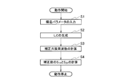
- 5 is a flowchart showing a processing procedure of the frequency selection board design device shown in FIG. 4. It is a figure which shows the example of the modeled correction circuit.
- the manner of calculating the S 21 of the resonant frequency f C of the corrected by multiplying a correction coefficient f C / f th to S 21 of the pre-correction resonant frequency f th is a diagram schematically illustrating. It is a block diagram showing an example of functional composition of a frequency selection board design device concerning a 2nd embodiment of the present invention. 13 is a flowchart showing a processing procedure of the frequency selection board design device shown in FIG. 12.
- unit cells of a resonator formed of a conductor pattern having a size equal to or smaller than the wavelength are arranged at a constant period p.
- the unit cell structure includes ring type, dipole array type, tri-hole type, patch type, and Jerusalem cross type.
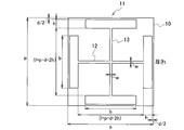
- FIG. 1 is a diagram schematically showing a plan view of a Jerusalem cross type unit cell.
- the Jerusalem cross type unit cell 11 is one in which a cross-shaped conductive pattern is formed on the dielectric substrate 10.
- the unit cells 11 are arranged on the dielectric substrate 10 at a constant period p.
- the thickness of the conductive pattern is t.
- a horizontal pattern 12 having a width w and a length l and a vertical pattern 13 having the same size form a cross
- a width h and a length b are provided at the respective ends of the horizontal pattern 12 and the vertical pattern 13.
- 4 has a shape in which four electrode patterns 4 are formed. The end portion of the electrode pattern 4 in the width h direction faces the electrode pattern 4 of the adjacent unit cells 11 of the same shape with a gap of the inter-electrode distance d.
- Each of the horizontal pattern 12 and the vertical pattern 13 forms an inductance L.
- each of the four electrode patterns 4 forms a capacitance C between the electrode patterns 4 of the adjacent unit cells 11.
- the shape of the unit cell 11 includes the period p of the unit cell 11, the width w of the horizontal pattern 12 and the vertical pattern 13, the length l of the horizontal pattern 12 and the vertical pattern 13, the width h of the electrode pattern 4, and the electrode pattern 4.
- the conductive pattern the thickness t of each conductive pattern, and the inter-electrode distance d.
- each structural parameter should be as follows. Since the inductance L is determined by the period p, the value of l / p may be set to about 0.7 to 0.9, for example. In the approximation of the inductance L, t ⁇ w is assumed, so t ⁇ 0.1w is preferable. Further, it is preferable that w ⁇ h ⁇ 0.1 to 0.3p, d / p ⁇ 0.01, and w ⁇ h, h / p> 0.3.
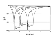
- FIG. 2 is a diagram showing the theoretical value f th of the resonance frequency calculated by the equation (3) and the resonance frequency obtained by the electromagnetic field analysis.
- Resonant frequency is indicated by the frequency characteristics of the insertion loss S 21.
- the solid line indicates the result of electromagnetic field analysis
- the broken line indicates the theoretical value f th .
- the parameter is the ratio p / ⁇ of the period p of the unit cell 11 and the incident wavelength ⁇ .
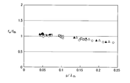
- FIG. 3 is a diagram showing the relationship between the ratio p / ⁇ of the period p of the unit cell 11 and the incident wavelength ⁇ , and the ratio fa / f th of the resonance frequency f a and the theoretical value f th obtained by electromagnetic field analysis. ..
- the resonance frequency f a obtained by the electromagnetic field analysis becomes about 70% of the theoretical value f th . That is, when the unit cell 11 is reduced, the deviation from the theoretical value f th increases.
- the frequency selection board design device 100 aims to reduce this deviation.
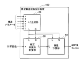
- FIG. 4 is a block diagram showing a functional configuration example of the frequency selection board designing device according to the first embodiment of the present invention.
- the frequency selection plate design device 100 shown in FIG. 4 includes an LC generation unit 20, a corrected resonance point calculation unit 30, and a characteristic calculation unit 40.
- the frequency selection board design device 100 is realized by, for example, a computer including a ROM, a RAM, a CPU, and the like.
- a computer including a ROM, a RAM, a CPU, and the like.
- the processing content of the function that each functional component should have is described by a program.
- FIG. 5 is a flowchart showing a processing procedure of the frequency selection board design device 100. The operation will be described with reference to FIG.
- the LC generation unit 20 receives as an input a structural parameter representing the structure of the unit cell 11 (step S1).
- the structural parameters are the period p of the unit cell 11, the width w of the horizontal pattern 12 and the vertical pattern 13, the length l of the horizontal pattern 12 and the vertical pattern 13, the width h of the electrode pattern 4, and the length b of the electrode pattern 4.
- Structural parameters are entered by the user.
- Each structural parameter has a preferable range as described above.
- the LC generation unit 20 generates the inductance L and the capacitor C based on the input structural parameters and the above equations (1) and (2) (step S2).
- the generated inductance L and capacitor C are output to the corrected resonance point calculator 30 and the characteristic calculator 40.
- the correction resonance point calculation unit 30 inputs the correction circuit to the number of calculations n input from the outside, the inductance L and the capacitance C generated by the LC generation unit 20 as inputs, and the distributed inductance L divided by the number of calculations n.
- a transmission line in which a virtual capacitance C V is connected in parallel to each of / n is modeled by a circuit terminated with a capacitance C.
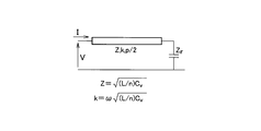
- the modeled correction circuit is shown in FIG.
- the virtual capacitor C V is connected in parallel to the distributed inductance L / n obtained by dividing the inductance L by n to form a transmission line, and the output of the transmission line is terminated by the capacitance C. Composed.
- phase difference ⁇ 'generated in the correction circuit is determined by the following equation from the telegraph equation.
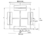
- FIG. 7 is a plan view schematically showing a plane of a Jerusalem cross type unit cell. As shown in FIG. 7, the electrode pattern 4 of the unit cell 11 is coupled with the electrode pattern 4 of the unit cell adjacent vertically and horizontally by the capacitance C.
- the unit cell 11 has the same vertical and horizontal cycle p, the same phase difference occurs in both the TM mode and the TE mode, and therefore the same can be applied. Since the number of divisions n represents the number of divisions of the correction circuit, if the number of divisions is increased, the amount of calculation increases, but the accuracy can be improved accordingly. In the above phase matching condition derivation, a sufficiently large number of divisions n is assumed.
- the correction circuit can be represented by the transmission line shown in FIG.
- the impedance Z ′ of the transmission line shown in FIG. 8 can be expressed by the following equation.
- Zr is the impedance of the capacitance C.
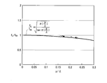
- FIG. 9 plots the resonance frequency obtained by electromagnetic field analysis of the unit cell 11 having the structural parameters shown in Table 1, and shows the correction coefficient of the equation (10) with a solid line.
- the horizontal axis of FIG. 9 is the ratio p / ⁇ of the period p of the unit cell 11 to the resonance wavelength, and the vertical axis is the correction coefficient f C / f th .
- the characteristic calculation unit 40 receives the inductance L and the capacitance C generated by the LC generation unit 20 and the corrected resonance frequency f C calculated by the corrected resonance point calculation unit 30 as input, and calculates the resonance frequency before correction from the inductance L and the capacitance C.
- f th is calculated, the correction resonance frequency f C is divided by the pre-correction resonance frequency f th to obtain a correction coefficient, and the reflection loss and the insertion loss before correction are multiplied by the correction coefficient to obtain the reflection loss and the insertion loss after correction. Is calculated (step S4).
- the frequency characteristics of S 11 and S 21 are calculated from the 4-terminal circuit of the impedance Z configured by the LC series resonance circuit including the inductance L and the capacitance C.
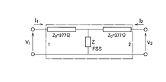
- FIG. 10 is a diagram showing a 4-terminal circuit.
- S 11 represents a reflection loss (return loss) of the terminal 1
- S 21 represents an insertion loss (insertion loss) from the terminal 1 to the terminal 2.
- Z 0 shown in FIG. 10 is a characteristic impedance in free space.
- characteristic calculation unit 40 calculates the S 11 and S 21 of the resonant frequency f C of the corrected by multiplying a correction coefficient f C / f th the frequency axis of the S 11 and S 21 of the pre-correction resonant frequency f th To do. According to this method, the L / C value is kept constant and the contour of the curve is not changed.
- Figure 11 is a diagram schematically showing how to calculate the S 21 of the resonant frequency f C of the corrected by multiplying a correction coefficient f C / f th to S 21 of the pre-correction resonant frequency f th.
- the experimental result is shown by a solid line and the simulation result is shown by a broken line.
- the frequency selection plate design device 100 is a frequency selection plate design device that supports the design of a frequency selection plate in which the unit cells 11 of the resonator are arranged on a plane.
- the LC generation unit 20 that generates the inductance L and the capacitance C of the unit cell 11 by inputting the structural parameters representing the structure of the unit cell 11, and the number of calculations n, the inductance L, and the capacitance C that are input from the outside, and the correction circuit.
- a characteristic calculation unit 40 that calculates the reflection loss S 11 and the insertion loss S 21 after correction is provided.
- the frequency characteristics can be accurately estimated from the structural parameters of the frequency selection plate.
- FIG. 12 is a block diagram showing a functional configuration example of a frequency selection board design device according to the second embodiment of the present invention.
- the frequency selection plate design apparatus 200 shown in FIG. 12 is different from the frequency selection plate design apparatus 100 (FIG. 4) in that the structure parameter resetting unit 240 is provided.
- FIG. 13 is a flowchart showing a processing procedure of the frequency selection board design device 200.
- the processing procedure of the frequency selection board design device 200 is different in that the processing steps of step S5 and subsequent steps are added to the processing procedure of the frequency selection board design device 100.
- the structural parameter resetting unit 250 calculates the difference between the corrected resonance frequency f C of the reflection loss S 11 and the insertion loss S 21 calculated by the characteristic calculation unit 40 and the desired resonance frequency f 0 input from the outside. Calculate (step S5).
- the frequency selection board design device 200 ends the operation (NO in step S6). If the difference is larger than the predetermined amount, the structure parameter is reset so that the difference becomes smaller (step S7).
- the resetting is performed by setting the width w of the horizontal pattern 12 and the vertical pattern 13, the length l of the horizontal pattern 12 and the vertical pattern 13, the width h of the electrode pattern 4, the length b of the electrode pattern 4, the thickness t of each conductive pattern, And one of the inter-electrode distances d is newly set.
- the structural parameter that determines the capacitance C is reset.
- the structural parameter that determines the inductance L is reset.
- the changing method is to increase the length l of the horizontal pattern 12 and the vertical pattern 13 and decrease the inter-electrode distance d and increase the length b of the electrode pattern 4 to decrease the frequency. To increase the frequency, the opposite is done.
- steps S3 to S7 are repeated until the difference becomes smaller than the predetermined amount.
- an existing algorithm such as a genetic algorithm (GA) can be used.
- the frequency selection plate design device 200 receives the corrected reflection loss and insertion loss calculated by the characteristic calculation unit 40, and the desired resonance frequency input from the outside, A structural parameter resetting unit 250 that finds the difference between the corrected resonant frequency f C and the desired resonant frequency f 0 and resets the structural parameter from the difference is provided. Repeat the setting of the structural parameters until it reaches the limit. Thereby, the accuracy of the frequency characteristics of the frequency selection plate can be improved.
- the frequency selection plate designing apparatus 100, 200 can quantitatively estimate the frequency characteristics of the frequency selection plate.
- the shape of the conductive pattern is described as an example of the Jerusalem cross type (FIG. 1), but the present invention is not limited to these examples.
- the present invention can be applied if the inductance L and the capacitor C can be formulated by the structural parameters.
- Terminal 10 Dielectric substrate 11: Unit cell 20: LC generation unit 30: Corrected resonance point calculation unit 40: Characteristic calculation unit 100, 200: Frequency selection plate design device 250: Structural parameter resetting unit
Landscapes
- Engineering & Computer Science (AREA)
- Physics & Mathematics (AREA)
- Computer Hardware Design (AREA)
- Theoretical Computer Science (AREA)
- Life Sciences & Earth Sciences (AREA)
- Bioinformatics & Cheminformatics (AREA)
- Bioinformatics & Computational Biology (AREA)
- Electromagnetism (AREA)
- Manufacturing & Machinery (AREA)
- Evolutionary Computation (AREA)
- Geometry (AREA)
- General Engineering & Computer Science (AREA)
- General Physics & Mathematics (AREA)
- Aerials With Secondary Devices (AREA)
- Filters And Equalizers (AREA)
Abstract
周波数選択板の構造パラメータからその周波数特性を精度良く推定する。構造パラメータを入力として単位セルのインダクタンスLとキャパシタンスCを生成するLC生成部20と、外部から入力される計算回数n、インダクタンスL、及びキャパシタンスCを入力として、補正回路を、インダクタンスLを計算回数nで分割した分布インダクタンスのそれぞれに仮想キャパシタンスが並列に接続された伝送線路がキャパシタンスCで終端される回路でモデル化し、補正回路のインピーダンスから補正共振周波数fCを計算する補正共振点計算部30と、インダクタンスL、キャパシタンスC、及び補正共振周波数fCを入力とし、インダクタンスLとキャパシタンスCから補正前共振周波数を計算し、補正共振周波数fCを補正前共振周波数で除して補正係数を求め、補正後の反射損失と挿入損失を計算する特性計算部40とを備える。
Description
本発明は、共振器の単位セルを平面上に配列した周波数選択板の設計を支援する周波数選択板設計装置に関する。
情報通信機器の小型化、高機能化が進み、無線LANやLTE等の回線を使った無線通信サービスが急速に普及している。これに伴い、無線通信端末からの電波の送受信が広域かつ頻繁に行われるようになり、周囲の他の電子機器への影響が懸念されている。
懸念される影響としては、無線環境の劣化、通信障害、及びセキュリティへの脅威などが考えられる。これらの影響を抑制する技術が求められている。
電波環境及び電磁環境を制御する目的で周波数選択板(FSS:Frequency Selective Surfaces)を用いることができる。周波数選択板は、波長と同程度以下の寸法の導体パターンで形成された共振器(単位セル)を周期的に配列することで、入射する電磁波の透過特性/反射特性に周波数依存性を持たせたものである。
周波数選択板には、様々な周波数特性を持つ共振構造が存在する。例えば、特定の周波数のみを反射するバンドストップフィルタ特性を持つものは、導体部を共振構造としたものが主であり、リング型、ダイポールアレイ型、トライホール型、パッチ型、及びエルサレムクロス型などがある(非特許文献1)。
周波数選択板は、考慮すべき構造パラメータの数が多く、パラメータがインダクタンス成分とキャパシタンス成分の増減に相反して関係する場合もある。また、単位セルの配列の仕方によってもその特性は変化し、理論として複雑である(非特許文献2)。
牧野 滋、「[チュートリアル講演]周波数選択板の基礎と応用」、信学技法、A・P 2015-5, Apl. 2015.
BEN A. MUNK,"Frequency Selective Surfaces Theory and Design",2000.
周波数選択板の構造パラメータから、既存の理論式に基づいてその周波数特性を推定することは可能である。しかし、実特性とのずれが大きく、それを改善する方法ない。つまり、周波数選択板の周波数特性を、その構造パラメータから物理原則に基づいて精度良く推定する方法がない。したがって、周波数選択板の設計は、コスト、労力を要するという課題がある。
本発明は、この課題に鑑みてなされたものであり、周波数選択板の構造パラメータからその周波数特性を精度良く推定することができる周波数選択板設計装置を提供することを目的とする。
本発明の一態様に係る周波数選択板設計装置は、共振器の単位セルを平面上に配列した周波数選択板の設計を支援する周波数選択板設計装置であって、前記単位セルの構造を表す構造パラメータを入力として該単位セルのインダクタンスとキャパシタンスを生成するLC生成部と、外部から入力される計算回数、前記インダクタンス、及び前記キャパシタンスを入力として、補正回路を、前記インダクタンスを前記計算回数で分割した分布インダクタンスのそれぞれに仮想キャパシタンスが並列に接続された伝送線路が前記キャパシタンスで終端される回路でモデル化し、前記仮想キャパシタンスは前記単位セルで生じる位相差と前記伝送線路で生じる位相差を整合させるものである前記補正回路のインピーダンスから補正共振周波数を計算する補正共振点計算部と、前記インダクタンス、前記キャパシタンス、及び前記補正共振周波数を入力とし、前記インダクタンスと前記キャパシタンスから補正前共振周波数を計算し、前記補正共振周波数を前記補正前共振周波数で除して補正係数を求め、補正前の反射損失と挿入損失にそれぞれ前記補正係数を乗じて補正後の反射損失と挿入損失を計算する特性計算部とを備えることを要旨とする。
本発明によれば、周波数選択板の構造パラメータからその周波数特性を精度良く推定することが出来る。
本発明の実施形態を説明する前に、本発明に係る共振器の単位セル、及びその構造パラメータついて図面を用いて説明する。
(単位セル)
周波数選択板は、波長と同程度以下の寸法の導体パターンで形成された共振器の単位セルが一定の周期pで配列される。単位セルの構造には、リング型、ダイポールアレイ型、トライホール型、パッチ型、及びエルサレムクロス型などがある。
周波数選択板は、波長と同程度以下の寸法の導体パターンで形成された共振器の単位セルが一定の周期pで配列される。単位セルの構造には、リング型、ダイポールアレイ型、トライホール型、パッチ型、及びエルサレムクロス型などがある。
この中で、共振周波数の定式化が比較的に容易なモデルは、エルサレムクロス型である。図1は、エルサレムクロス型の単位セルの平面図を模式的に示す図である。
図1に示すようにエルサレムクロス型の単位セル11は、誘電体基板10の上に十字状の導電パターンを形成したものである。単位セル11は一定の周期pで誘電体基板10の上に配置される。導電パターンの厚さはtである。
導電パターンの形状は、幅w、長さlの横パターン12と、同寸法の縦パターン13が十字を形成し、横パターン12と縦パターン13のそれぞれの端部には幅h、長さbの電極パターン4が4つ形成される形状である。電極パターン4の幅h方向の端部は、隣接する同形状の単位セル11の電極パターン4と電極間距離dの間隔を空けて対向する。
横パターン12と縦パターン13のそれぞれはインダクタンスLを形成する。また、4つの電極パターン4のそれぞれは、隣接する単位セル11の電極パターン4との間でキャパシタンスCを形成する。
このように単位セル11の形状は、単位セル11の周期p、横パターン12と縦パターン13の幅w、横パターン12と縦パターン13の長さl、電極パターン4の幅h、電極パターン4の長さb、各導電パターンの厚さt、及び電極間距離dによって特定される。
以降、単位セル11の形状を特定するこれらのパラメータを構造パラメータと称する。この構造パラメータによって、単位セル11のインダクタンスLとキャパシタンスCは、次式で表せる。
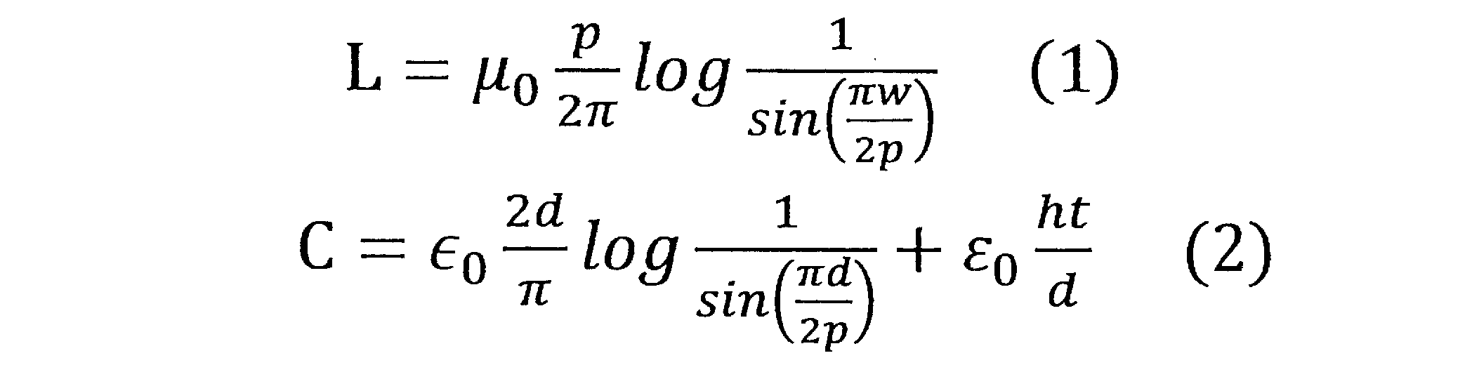
ここで周期pは、p=l+d+2hで表せる。
なお、構造パラメータのそれぞれの値は、次のようにすると良い。インダクタンスLは、周期pによって決定されるので、l/pの値は例えば0.7~0.9程度にすると良い。またインダクタンスLの近似では、t≪wを仮定しているのでt<0.1wとすると良い。また、w≪h≦0.1~0.3p程度、d/p≧0.01程度、w≪h,h/p>0.3程度にすると良い。
共振周波数の理論値fthは次式で表せる。

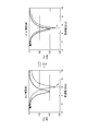
図2は、式(3)で計算した共振周波数の理論値fthと、電磁界解析で求めた共振周波数を示す図である。共振周波数は、挿入損失S21の周波数特性で示す。図2において、実線は電磁界解析の結果、破線は理論値fthである。また、パラメータは、単位セル11の周期pと入射波長λの比p/λとした。
図2に示すように、電磁界解析の結果と理論値fthとの間に乖離が見られる。その乖離は、パラメータのp/λが大きくなるほど増加する。
図3は、単位セル11の周期pと入射波長λの比p/λと、電磁界解析で求めた共振周波数faと理論値fthの比fa/fthとの関係を示す図である。図3に示すようにp/λ=0.1付近から、共振周波数の理論値fthからの乖離が増え始め、単位セル11の周期pが理論値fthの波長の1/4倍(0.25)になると、電磁界解析で求めた共振周波数faは理論値fthの70%程度になる。つまり、単位セル11を小さくすると理論値fthとの乖離が大きくなる。
本実施形態に係る周波数選択板設計装置100は、この乖離を小さくすることを目的とする。
以下、本発明の実施形態について図面を用いて説明する。複数の図面中同一のものには同じ参照符号を付し、説明は繰り返さない。
〔第1実施形態〕
図4は、本発明の第1実施形態に係る周波数選択板設計装置の機能構成例を示すブロック図である。図4に示す周波数選択板設計装置100は、LC生成部20、補正共振点計算部30、及び特性計算部40を備える。
図4は、本発明の第1実施形態に係る周波数選択板設計装置の機能構成例を示すブロック図である。図4に示す周波数選択板設計装置100は、LC生成部20、補正共振点計算部30、及び特性計算部40を備える。
周波数選択板設計装置100は、例えば、ROM、RAM、CPU等からなるコンピュータで実現される。各機能構成部をコンピュータによって実現する場合、各機能構成部が有すべき機能の処理内容はプログラムによって記述される。
図5は、周波数選択板設計装置100の処理手順を示すフローチャートである。図5も参照してその動作を説明する。
LC生成部20は、単位セル11の構造を表す構造パラメータを入力とする(ステップS1)。構造パラメータは、上記の単位セル11の周期p、横パターン12と縦パターン13の幅w、横パターン12と縦パターン13の長さl、電極パターン4の幅h、電極パターン4の長さb、各導電パターンの厚さt、及び電極間距離dである。構造パラメータは、利用者によって入力される。各構造パラメータには、上記のように好ましい範囲がある。
次に、LC生成部20は、入力された構造パラメータに基づいて、上記の式(1)と式(2)に基づいてインダクタンスLとキャパシタCを生成する(ステップS2)。生成されたインダクタンスLとキャパシタCは、補正共振点計算部30と特性計算部40に出力される。
補正共振点計算部30は、補正回路を、外部から入力される計算回数n、LC生成部20で生成されたインダクタンスLとキャパシタンスCを入力として、インダクタンスLを計算回数nで分割した分布インダクタンスL/nのそれぞれに仮想キャパシタンスCVが並列に接続された伝送線路が、キャパシンタンスCで終端される回路でモデル化する。モデル化した補正回路を図6に示す。
図6に示すように、補正回路は、インダクタンスLをn分割した分布インダクタンスL/nに仮想キャパシタCVが並列に接続されて伝送路化され、その伝送路の出力がキャパシタンスCで終端されて構成される。
補正回路で生じる位相差Δφ′は、電信方程式から次式によって定まる。

ここで実際の位相差を、エルサレムクロス型の単位セルで考える。
図7は、エルサレムクロス型の単位セルの平面を模式的に示す平面図である。図7に示すように、単位セル11の電極パターン4は、縦横に隣接する単位セルの電極パターン4との間でキャパシタンスCで結合する。
図7において、単位セル11の中心に対して片方の半分の面をn分割したときに発生する位相差は式(5)で表せる。

なお、従来この位相差(式(5))は考慮されていなかった。そのために、単位セル11を小さくすると理論値fthとの乖離が大きくなる(図3)。
したがって、補正回路で生じる単位位相差Δφ′と、実際の単位位相差Δφを等しくする(式(6))ようにすれば、適切な共振周波数を計算することが可能になる。

式(6)から仮想キャパシタンスCVを求めると式(7)で表せる。

自由空間の電磁波の分散関係kc0=ωで伝搬する入射電磁波と結合することを踏まえると、次式(8)が得られる。

ここでc0は真空中の光速である。つまり、周期pとインダクタンスLと分割数nが決定すれば、実特性を模擬した適切な周波数設計が可能になる。例えば、周期p=10mm、n=50、L=6.4×10⁹Hとすると、仮想キャパシタンスCV≒0.0036pfとなる。
また、単位セル11の縦横の周期pが同じ場合、TMモード、TEモードのどちらでも同じ位相差が発生するため同様に適用可能である。分割数nは、補正回路の分割数を表すため、大きくすると計算量は多くなるが、その分、精度を上げることができる。上記の位相整合条件導出には、十分に大きな数の分割数nを仮定している。
補正回路におけるインピーダンスを考えたとき、分割数nが十分大きいと仮定し、kΔx=kと見る。そうすると、補正回路は、図8に示す伝送路で表すことができる。図8に示す伝送線路のインピーダンスZ′は次式で表せる。Zrは、キャパシタンスCのインピーダンスである。

共振条件Z′=0より、補正共振周波数fCと、式(3)で計算した補正前共振周波数fthとの関係は、単位セル11の周期pと共振波長の比p/λを用いて式(10)で表せる。式(10)は補正係数を意味する。

単位セル11の構造パラメータを変化させて電磁界解析で求めた共振周波数と、式(10)で求めた補正共振周波数fCの比較を行った。表1に、電磁界解析を行った単位セル11の構造パラメータを示す。
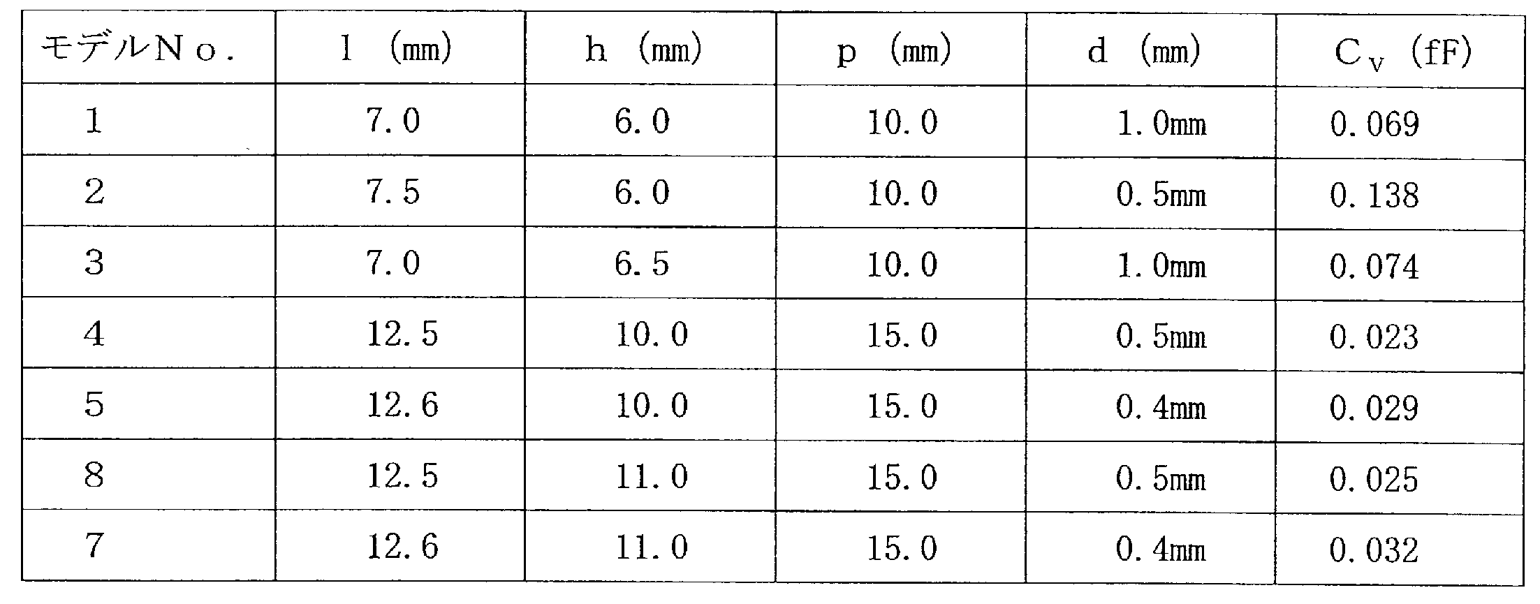
図9は、表1に示す構造パラメータの単位セル11を電磁界解析して求めた共振周波数をプロットし、式(10)の補正係数を実線で示す。図9の横軸は単位セル11の周期pと共振波長の比p/λ、縦軸は補正係数fC/fthである。
図9に示すように、理論曲線(式(10))と、電磁界解析して求めた共振周波数は良く一致する。このように補正係数は、補正前共振周波数fthと補正共振周波数fCを良く一致させる。
特性計算部40は、LC生成部20で生成されたインダクタンスLとキャパシタンスC、及び補正共振点計算部30で計算された補正共振周波数fCを入力として、インダクタンスLとキャパシタンスCから補正前共振周波数fthを計算し、補正共振周波数fCを補正前共振周波数fthで除して補正係数を求め、補正前の反射損失と挿入損失にそれぞれ補正係数を乗じて補正後の反射損失と挿入損失を計算する(ステップS4)。
補正前共振周波数fthは、インダクタンスLとキャパシタンスCからなるLC直列共振回路で構成されるインピーダンスZの4端子回路からS11とS21の周波数特性を算出する。図10は、4端子回路を示す図である。
S11は端子1の反射損失(リターンロス)、S21は端子1から端子2への挿入損失(インサーションロス)を表す。図10に示すZ0は、自由空間の特性インピーダンスである。
次に、特性計算部40は、補正前共振周波数fthのS11とS21の周波数軸に補正係数fC/fthを乗じて補正後の共振周波数fCのS11とS21を計算する。この方法によれば、L/Cの値を一定に保ち曲線の外形を変化させない。
図11は、補正前共振周波数fthのS21に補正係数fC/fthを乗じて補正後の共振周波数fCのS21を計算する様子を模式的に示す図である。実験結果を実線、シミュレーション結果を破線で示す。
図11に示すように、補正後の共振周波数は、実験結果の周波数(実線)に近づいていることが分かる。
以上説明したように、本実施形態に係る周波数選択板設計装置100は、共振器の単位セル11を平面上に配列した周波数選択板の設計を支援する周波数選択板設計装置であって、単位セル11の構造を表す構造パラメータを入力として該単位セル11のインダクタンスLとキャパシタンスCを生成するLC生成部20と、外部から入力される計算回数n、インダクタンスL、及びキャパシタンスCを入力として、補正回路を、インダクタンスLを計算回数nで分割した分布インダクタンスのそれぞれに仮想キャパシタンスCVが並列に接続された伝送線路がキャパシタンスCで終端される回路でモデル化し、仮想キャパシタンスCVは単位セル11で生じる位相差と伝送線路で生じる位相差を整合させるものである補正回路のインピーダンスから補正共振周波数fCを計算する補正共振点計算部30と、インダクタンスL、キャパシタンスC、及び補正共振周波数fCを入力とし、インダクタンスLとキャパシタンスCから補正前共振周波数fthを計算し、補正共振周波数fCを補正前共振周波数fthで除して補正係数fC/fthを求め、補正前の反射損失S11と挿入損失S21にそれぞれ補正係数fC/fthを乗じて補正後の反射損失S11と挿入損失S21を計算する特性計算部40とを備える。
これにより、周波数選択板の構造パラメータからその周波数特性を精度良く推定することが出来る。
〔第2実施形態〕
図12は、本発明の第2実施形態に係る周波数選択板設計装置の機能構成例を示すブロック図である。図12に示す周波数選択板設計装置200は、構造パラメータ再設定部240を備える点で周波数選択板設計装置100(図4)と異なる。
図12は、本発明の第2実施形態に係る周波数選択板設計装置の機能構成例を示すブロック図である。図12に示す周波数選択板設計装置200は、構造パラメータ再設定部240を備える点で周波数選択板設計装置100(図4)と異なる。
図13は、周波数選択板設計装置200の処理手順を示すフローチャートである。周波数選択板設計装置200の処理手順は、周波数選択板設計装置100の処理手順に対してステップS5以降の手順が追加される点で異なる。
構造パラメータ再設定部250は、特性計算部40で計算された補正後の反射損失S11及び挿入損失S21の共振周波数fCと、外部から入力される所望の共振周波数f0との差分を計算する(ステップS5)。
構造パラメータ再設定部250で計算された差分が、所定量よりも小さければ、周波数選択板設計装置200は動作を終了する(ステップS6のNO)。また、差分が所定量よりも大きければ差分が小さくなるように構造パラメータを再設定する(ステップS7)。
再設定は、横パターン12と縦パターン13の幅w、横パターン12と縦パターン13の長さl、電極パターン4の幅h、電極パターン4の長さb、各導電パターンの厚さt、及び電極間距離dの何れかを新たに設定する。差分が大きい場合は、キャパシタンスCを決める構造パラメータを再設定する。差分を微調整する場合は、インダクタンスLを決める構造パラメータを再設定する。
差分が大きい場合は、電極間距離dを変更する。また、差分が小さい場合は、横パターン12と縦パターン13の長さl又は電極パターン4の長さbを変更する。
変更方法は、周波数を低くする場合は、横パターン12と縦パターン13の長さlを大きく、電極間距離dを小さく、電極パターン4の長さbを大きくの何れか又はその全部を行う。周波数を高くする場合は、その逆を行う。
構造パラメータが再設定された後は、差分が所定量よりも小さくなるまでステップS3~S7を繰り返す。この差分を最適化するアルゴリズムには、例えば遺伝アルゴリズム(GA)等の既存のアルゴリズムを用いることができる。
以上述べたように、本実施形態に係る周波数選択板設計装置200は、特性計算部40で計算された補正後の反射損失と挿入損失、及び外部から入力される所望の共振周波数を入力とし、補正後の共振周波数fCと所望の共振周波数f0の差を求め、該差から構造パラメータを再設定する構造パラメータ再設定部250を備え、構造パラメータ再設定部250は、差が所定の大きさになるまで構造パラメータの再設定を繰り返す。これにより、周波数選択板の周波数特性の精度を高めることができる。
以上説明したように本実施形態に係る周波数選択板設計装置100,200によれば、周波数選択板の周波数特性を定量的に推定することができる。なお、上記の実施形態の説明において、導電パターンの形状は、エルサレムクロス型(図1)の例で説明したが、本発明はこれらの例に限定されない。構造パラメータによってインダクタンスL及びキャパシタCが定式化できれば、本発明を適用することができる。
このように、本発明はここでは記載していない様々な実施形態等を含むことは勿論である。したがって、本発明の技術的範囲は上記の説明から妥当な特許請求の範囲に係る発明特定事項によってのみ定められるものである。
1、2:端子
10:誘電体基板
11:単位セル
20:LC生成部
30:補正共振点計算部
40:特性計算部
100、200:周波数選択板設計装置
250:構造パラメータ再設定部
10:誘電体基板
11:単位セル
20:LC生成部
30:補正共振点計算部
40:特性計算部
100、200:周波数選択板設計装置
250:構造パラメータ再設定部
Claims (5)
- 共振器の単位セルを平面上に配列した周波数選択板の設計を支援する周波数選択板設計装置であって、
前記単位セルの構造を表す構造パラメータを入力として該単位セルのインダクタンスとキャパシタンスを生成するLC生成部と、
外部から入力される計算回数、前記インダクタンス、及び前記キャパシタンスを入力として、補正回路を、前記インダクタンスを前記計算回数で分割した分布インダクタンスのそれぞれに仮想キャパシタンスが並列に接続された伝送線路が前記キャパシタンスで終端される回路でモデル化し、前記仮想キャパシタンスは前記単位セルで生じる位相差と前記伝送線路で生じる位相差を整合させるものである前記補正回路のインピーダンスから補正共振周波数を計算する補正共振点計算部と、
前記インダクタンス、前記キャパシタンス、及び前記補正共振周波数を入力とし、前記インダクタンスと前記キャパシタンスから補正前共振周波数を計算し、前記補正共振周波数を前記補正前共振周波数で除して補正係数を求め、補正前の反射損失と挿入損失にそれぞれ前記補正係数を乗じて補正後の反射損失と挿入損失を計算する特性計算部と
を備えることを特徴とする周波数選択板設計装置。 - 前記単位セルは、
誘電体基板の上に十字状の導電パターンを形成したものであって、十字を形成する横パターンと縦パターンは、それぞれの方向に所定の長さ延長され、その所定の長さ延長された先は直交する誘電体基板上の両方向に、前記横パターン及び前記縦パターンの幅よりも太い幅の導電パターンが所定の長さ延長された導電パターンを備え、
前記構造パラメータは、当該導電パターンの形状を特定するものである
ことを特徴とする請求項1に記載の周波数選択板設計装置。 - 前記分布インダクタンスは、前記インダクタンスを前記計算回数のnで等分割した値であり、
前記仮想キャパシタンスは、前記単位セルの中心に対して片方の半分の表面を前記nで分割した場合に発生する位相差と、前記伝送線路の単位位相差とを等しくする位相整合条件から求めた値であり、
前記補正共振周波数は、計算された複数の共振周波数の中で最も低い共振周波数である
ことを特徴とする請求項1又は2に記載の周波数選択板設計装置。 - 前記補正前共振周波数は、
前記インダクタンスと前記キャパシタンスを直列に接続させたLC直列共振回路の共振周波数である
ことを特徴とする請求項1乃至3の何れかに記載の周波数選択板設計装置。 - 前記特性計算部で計算された補正後の反射損失と挿入損失、及び外部から入力される所望の共振周波数を入力とし、補正後の共振周波数と前記所望の共振周波数の差を求め、該差から前記構造パラメータを再設定する構造パラメータ再設定部を
備え、
前記構造パラメータ再設定部は、
前記差が所定の大きさになるまで前記構造パラメータの再設定を繰り返す
ことを特徴とする請求項1乃至4の何れかに記載の周波数選択板設計装置。
Priority Applications (1)
| Application Number | Priority Date | Filing Date | Title |
|---|---|---|---|
| US17/289,835 US11588248B2 (en) | 2018-10-30 | 2019-10-16 | Frequency selective surface designing device |
Applications Claiming Priority (2)
| Application Number | Priority Date | Filing Date | Title |
|---|---|---|---|
| JP2018203815A JP6944118B2 (ja) | 2018-10-30 | 2018-10-30 | 周波数選択板設計装置 |
| JP2018-203815 | 2018-10-30 |
Publications (1)
| Publication Number | Publication Date |
|---|---|
| WO2020090482A1 true WO2020090482A1 (ja) | 2020-05-07 |
Family
ID=70464425
Family Applications (1)
| Application Number | Title | Priority Date | Filing Date |
|---|---|---|---|
| PCT/JP2019/040738 Ceased WO2020090482A1 (ja) | 2018-10-30 | 2019-10-16 | 周波数選択板設計装置 |
Country Status (3)
| Country | Link |
|---|---|
| US (1) | US11588248B2 (ja) |
| JP (1) | JP6944118B2 (ja) |
| WO (1) | WO2020090482A1 (ja) |
Families Citing this family (2)
| Publication number | Priority date | Publication date | Assignee | Title |
|---|---|---|---|---|
| KR102363140B1 (ko) * | 2020-05-13 | 2022-02-15 | 한국표준과학연구원 | 주파수 선택 표면 필터 설계 방법과 컴퓨터 프로그램을 저장하는 저장 매체 |
| KR102754714B1 (ko) * | 2023-07-13 | 2025-01-21 | 한국표준과학연구원 | 다중공진 필터 설계 방법과 컴퓨터 프로그램을 저장하는 저장 매체 |
Citations (2)
| Publication number | Priority date | Publication date | Assignee | Title |
|---|---|---|---|---|
| US20080062059A1 (en) * | 2006-07-07 | 2008-03-13 | Angelo Freni | Antenna, method of manufacturing an antenna and apparatus for manufacturing an antenna |
| JP2014155102A (ja) * | 2013-02-12 | 2014-08-25 | Yokohama Rubber Co Ltd:The | 曲面への周波数選択素子の配列決定方法 |
Family Cites Families (8)
| Publication number | Priority date | Publication date | Assignee | Title |
|---|---|---|---|---|
| US8207907B2 (en) * | 2006-02-16 | 2012-06-26 | The Invention Science Fund I Llc | Variable metamaterial apparatus |
| KR101086743B1 (ko) * | 2006-08-25 | 2011-11-25 | 레이스팬 코포레이션 | 메타물질 구조물에 기초된 안테나 |
| JP6052388B2 (ja) * | 2013-02-22 | 2016-12-27 | 株式会社村田製作所 | センサタグ、センサタグの製造方法 |
| US10014570B2 (en) * | 2013-05-13 | 2018-07-03 | The Board Of Trustees Of The Leland Stanford Junior University | Single transducer for data and power in wirelessly powered devices |
| FR3023401B1 (fr) * | 2014-07-07 | 2017-10-13 | Commissariat Energie Atomique | Accord en frequence d'une etiquette electronique |
| TR201412400A1 (tr) * | 2014-10-22 | 2016-05-23 | Aselsan Elektronik Sanayi Ve Ticaret As | Geniş bantlı ve çok katmanlı radar soğurucular için hızlı ve doğru tasarım yöntemi. |
| KR102127364B1 (ko) * | 2019-07-19 | 2020-06-26 | 재단법인 파동에너지 극한제어 연구단 | 스텔스 구조체의 설계방법 및 이에 의해 설계되는 스텔스 구조체 |
| CN112733397B (zh) * | 2020-12-28 | 2023-03-24 | 桂林电子科技大学 | 针对三种方形螺旋结构电磁超材料单元的设计方法 |
-
2018
- 2018-10-30 JP JP2018203815A patent/JP6944118B2/ja active Active
-
2019
- 2019-10-16 WO PCT/JP2019/040738 patent/WO2020090482A1/ja not_active Ceased
- 2019-10-16 US US17/289,835 patent/US11588248B2/en active Active
Patent Citations (2)
| Publication number | Priority date | Publication date | Assignee | Title |
|---|---|---|---|---|
| US20080062059A1 (en) * | 2006-07-07 | 2008-03-13 | Angelo Freni | Antenna, method of manufacturing an antenna and apparatus for manufacturing an antenna |
| JP2014155102A (ja) * | 2013-02-12 | 2014-08-25 | Yokohama Rubber Co Ltd:The | 曲面への周波数選択素子の配列決定方法 |
Non-Patent Citations (1)
| Title |
|---|
| CHEN ET AL.: "Fast Design of Jerusalem-Cross Parameters by Equivalent circuit Model and Least-Square Curve Fitting Technique", ACES JOURNAL, vol. 30, no. 7, July 2015 (2015-07-01), pages 717 - 730, XP055702882 * |
Also Published As
| Publication number | Publication date |
|---|---|
| JP6944118B2 (ja) | 2021-10-06 |
| US20210408693A1 (en) | 2021-12-30 |
| US11588248B2 (en) | 2023-02-21 |
| JP2020072329A (ja) | 2020-05-07 |
Similar Documents
| Publication | Publication Date | Title |
|---|---|---|
| CN116136938B (zh) | 声表面波器件仿真参数的快速拟合方法、系统及相关设备 | |
| CN106712738B (zh) | 根据频率响应要求设计声微波滤波器的方法 | |
| CN107169232B (zh) | 声波滤波器电路模型参数的提取方法及装置 | |
| WO2020090482A1 (ja) | 周波数選択板設計装置 | |
| CN107562990B (zh) | 基于bvd模型的baw滤波器设计方法、装置及设备 | |
| CN116467998A (zh) | 一种基于等效电路的极化转换超表面快速计算方法及系统 | |
| Abunjaileh et al. | A circuit-theoretic approach to the design of quadruple-mode broadband microstrip patch antennas | |
| CN115455823A (zh) | 基于相位调控的阵列天线带宽扩展方法、装置及阵列天线 | |
| CN113225039B (zh) | 基于拓扑绝缘体的鲁棒性谐振器 | |
| CN116187258B (zh) | 量子芯片版图的仿真方法、装置、计算设备及存储介质 | |
| CN108449067B (zh) | 体声波滤波器 | |
| Ouyang et al. | Conformal antenna optimization with space mapping | |
| Fan et al. | A sequentially coupled filter design approach using the reflected group delay method and the implicit space mapping technique | |
| CN117454723A (zh) | 基于玻璃通孔技术的毫米波封装天线的仿真方法及装置 | |
| CN116029247A (zh) | 一种三销钉阻抗调配器的路径规划方法 | |
| Savin et al. | Mode matching technique for tunable shielded cylindrical metal-dielectric resonator | |
| CN111181524B (zh) | 高阶全通二端口网络及其构建方法 | |
| Yang et al. | Fast transient analysis method for lossy nonuniform transmission line with nonlinear terminations | |
| CN113901752A (zh) | 一种器件仿真模型的构建方法及装置 | |
| Zhang et al. | Cognition-driven formulation of space mapping for reducing gain variation of antennas | |
| CN105676002A (zh) | 一种微带天线品质因数提取方法 | |
| Pons-Abenza et al. | Frequency correction design technique for additive manufactured cavity filters | |
| Sun et al. | The irregularly shaped patch as a perturbation of a regularly shaped patch | |
| CN104134862B (zh) | 圆形贴片微带天线谐振频率计算方法 | |
| CN104300938B (zh) | 均衡由耦合损耗引起的失真的方法及利用其生产的滤波器 |
Legal Events
| Date | Code | Title | Description |
|---|---|---|---|
| 121 | Ep: the epo has been informed by wipo that ep was designated in this application |
Ref document number: 19880873 Country of ref document: EP Kind code of ref document: A1 |
|
| NENP | Non-entry into the national phase |
Ref country code: DE |
|
| 122 | Ep: pct application non-entry in european phase |
Ref document number: 19880873 Country of ref document: EP Kind code of ref document: A1 |