WO2020084768A1 - 光拡散部材および液晶表示装置 - Google Patents
光拡散部材および液晶表示装置 Download PDFInfo
- Publication number
- WO2020084768A1 WO2020084768A1 PCT/JP2018/039893 JP2018039893W WO2020084768A1 WO 2020084768 A1 WO2020084768 A1 WO 2020084768A1 JP 2018039893 W JP2018039893 W JP 2018039893W WO 2020084768 A1 WO2020084768 A1 WO 2020084768A1
- Authority
- WO
- WIPO (PCT)
- Prior art keywords
- light
- layer
- liquid crystal
- substrate
- diffusing member
- Prior art date
- Legal status (The legal status is an assumption and is not a legal conclusion. Google has not performed a legal analysis and makes no representation as to the accuracy of the status listed.)
- Ceased
Links
Images


Classifications
-
- G—PHYSICS
- G02—OPTICS
- G02B—OPTICAL ELEMENTS, SYSTEMS OR APPARATUS
- G02B5/00—Optical elements other than lenses
- G02B5/02—Diffusing elements; Afocal elements
-
- G—PHYSICS
- G02—OPTICS
- G02F—OPTICAL DEVICES OR ARRANGEMENTS FOR THE CONTROL OF LIGHT BY MODIFICATION OF THE OPTICAL PROPERTIES OF THE MEDIA OF THE ELEMENTS INVOLVED THEREIN; NON-LINEAR OPTICS; FREQUENCY-CHANGING OF LIGHT; OPTICAL LOGIC ELEMENTS; OPTICAL ANALOGUE/DIGITAL CONVERTERS
- G02F1/00—Devices or arrangements for the control of the intensity, colour, phase, polarisation or direction of light arriving from an independent light source, e.g. switching, gating or modulating; Non-linear optics
- G02F1/01—Devices or arrangements for the control of the intensity, colour, phase, polarisation or direction of light arriving from an independent light source, e.g. switching, gating or modulating; Non-linear optics for the control of the intensity, phase, polarisation or colour
- G02F1/13—Devices or arrangements for the control of the intensity, colour, phase, polarisation or direction of light arriving from an independent light source, e.g. switching, gating or modulating; Non-linear optics for the control of the intensity, phase, polarisation or colour based on liquid crystals, e.g. single liquid crystal display cells
- G02F1/133—Constructional arrangements; Operation of liquid crystal cells; Circuit arrangements
- G02F1/1333—Constructional arrangements; Manufacturing methods
- G02F1/1335—Structural association of cells with optical devices, e.g. polarisers or reflectors
Definitions
- the present invention relates to a light diffusing member and a liquid crystal display device.
- VA Vertical Alignment
- IPS In-Plane Switching
- the VA type liquid crystal display device has a higher contrast ratio (front CR) when viewed from the front, but has a worse viewing angle than the IPS type liquid crystal display device.
- Patent Documents 1 and 2 As a trial to improve the color viewing angle dependency of a liquid crystal display device, a technique of diffusing light transmitted through a liquid crystal panel has been proposed (Patent Documents 1 and 2).
- Patent Document 1 a light scattering layer in which a scatterer is dispersed in a resin is arranged on the display surface of a liquid crystal panel to scatter light transmitted through the liquid crystal panel.
- Patent Document 2 a liquid crystal panel is provided by using a viewing angle widening film including a light diffusing member that utilizes total reflection of light and a diffusing layer in which a large number of light scatterers are dispersed inside a binder resin. It diffuses the transmitted light.
- Patent Document 2 not only provides a liquid crystal display device having a high front CR in a dark place and a wide viewing angle, but also improves blurring of the display in the liquid crystal display device.
- Patent Document 3 and Non-Patent Documents 1 and 2 will be described later.
- Patent Document 1 reduces the front CR in the bright place of the liquid crystal display device due to the return light of the external light from the diffusion layer.
- the viewing angle widening film of Patent Document 2 also lowers the front CR in the bright place of the liquid crystal display device.
- the present invention has been made in view of such conventional problems, and realizes a liquid crystal display device that has a function comparable to that of the viewing angle widening film of Patent Document 2 and that has excellent front CR in a bright place.
- An object of the present invention is to provide a light diffusing member and a liquid crystal display device including the light diffusing member.
- a light diffusing member includes a base material having a first surface and a second surface facing each other, a first layer laminated on a predetermined region of the second surface of the base material, and the first layer.
- a first portion made of a first material and a second portion made of a second material extending over the surface of the third layer and occupying a region excluding the first portion are formed, and the second layer and the second layer are formed.
- a cross-sectional shape of the third layer perpendicular to the first surface is a tapered shape that spreads in a direction away from the base material, and the first material has a larger refractive index than the second material,
- the two layers are made of a binder resin in which a plurality of light scattering particles are dispersed, and the taper angle in the third layer is 0 ° is less than or equal to.
- the light that has entered the third layer is diffused by total reflection in the first part, and then proceeds toward the second layer.
- the light is scattered and then emitted from the first side of the substrate.
- the light is generally scattered forward and the backward scattering is reduced.
- the liquid crystal display device using the light diffusing member of the present embodiment achieves an excellent dark place contrast ratio, a wide viewing angle (color viewing angle and luminance viewing angle), and an excellent bright place contrast ratio.
- the light diffusing member also has a tapered surface formed on the second layer. Therefore, light is diffused by total reflection not only in the third layer but also in the second layer.
- the liquid crystal display device employing the light diffusing member of the present embodiment can exhibit a viewing angle (color viewing angle and luminance viewing angle) superior to that of the light diffusing member of Patent Document 3.
- a viewing angle color viewing angle and luminance viewing angle
- the tapered surface is formed also in the second layer, in the structure of Patent Document 3, a part of the light absorbed in the first layer is totally reflected by the tapered surface of the second layer. As a result, the light transmittance is improved.
- a liquid crystal display device is a liquid crystal layer containing a liquid crystal composition, which is held between the above-mentioned light diffusing member, a first substrate and a second substrate which are bonded to face each other.
- a light source section including a light source, wherein the director of the liquid crystal composition is substantially perpendicular to the first substrate and the second substrate when no voltage is applied, Includes a light condensing member that condenses light from the light source and emits the light toward the first substrate, and the second substrate is in contact with the third layer of the light diffusing member.
- the director of the liquid crystal composition is substantially perpendicular to the first substrate and the second substrate when no voltage is applied. Then, the light emitted from the light source section and entering the third layer of the light diffusing member is diffused by total reflection in the first section, and then proceeds toward the second layer. The light is scattered in the second layer and then emitted from the first side of the substrate. In the second layer, the light is scattered generally forward, so that the backward scattering is reduced.
- the liquid crystal display device according to the embodiment of the present invention achieves an excellent dark place contrast ratio, a wide viewing angle (color viewing angle and luminance viewing angle) and an excellent bright place contrast ratio.
- a light diffusing member and a light diffusing member for realizing a liquid crystal display device having an excellent front CR in a bright place while having a function comparable to the viewing angle widening film disclosed in Patent Document 2 and the like. It is possible to provide a liquid crystal display device provided with.
- FIG. 1 is a schematic sectional view of a light diffusing member according to an embodiment of the present invention.
- FIG. 2 is a schematic schematic view showing an example of the method for manufacturing the light diffusing member according to the embodiment of the present invention.
- FIG. 3 is a schematic schematic view showing an example of the method for manufacturing the light diffusing member according to the embodiment of the present invention.
- FIG. 4 is a schematic diagram of a liquid crystal display device according to an embodiment of the present invention.
- FIG. 1 is a schematic cross-sectional view of the light diffusion member 1 of this embodiment. It should be noted that the materials, shapes, and relative positional relationships between the constituent elements in the embodiments described below are all examples. Therefore, the light diffusion member 1 of the present embodiment is not limited to these examples.
- the light diffusing member 1 of the present embodiment has a base material 2 having a front surface (an example of the first surface) 21 and a back surface (an example of the second surface) 22 that is the opposite surface thereof, and a back surface 22 of the base material 2.
- the light-shielding layer 3 (an example of the first layer) laminated in a predetermined region of the above, the scattering layer 4 (an example of the second layer) that covers the back surface 22 of the base material 2 while avoiding the light-shielding layer 3, and the scattering layer 4.
- the laminated diffusion layer 5 (an example of a third layer) is provided. As shown in FIG. 1, the light diffusing member 1 has a tapered portion 52 formed so as to penetrate the scattering layer 4 and the diffusing layer 5.
- One end of the tapered portion 52 is open to the outside of the light diffusing member 1, and the other end is closed by the light shielding layer 3 arranged on the back surface 22 of the base material 2. That is, the light shielding layer 3 and the tapered portion 52 are substantially aligned in the thickness direction of the base material 2.
- the material forming the base material 2 is not particularly limited.
- the material forming the substrate is preferably a resin such as a thermoplastic polymer, a thermosetting resin, or a photopolymerizable resin, and polyethylene terephthalate (PET), triacetyl cellulose (TAC), polycarbonate (PC), polyethylene.
- PET polyethylene terephthalate
- TAC triacetyl cellulose
- PC polycarbonate
- a transparent resin such as a naphthalate (PEN) or polyether sulfone (PES) film is more preferable.
- the base material 2 made of PET is used.
- the front surface 21 is a light emitting surface from which the light diffused by the scattering layer 4 and the diffusion layer 5 described later is extracted.
- the thickness of the base material 2 is not particularly limited.
- the light shielding layer 3 is a layer laminated on a predetermined region of the back surface 22 of the base material 2, and is a part of the external light (light from the outside of the light diffusion member 1) received by the front surface 21 of the base material 2. Is absorbed to prevent a decrease in contrast ratio (CR) in a bright place.
- the light-shielding layer 3 is formed of a multilayer film made of chromium, a metal such as chromium / chromium oxide, or a photoresist in which carbon particles are dispersed in a photosensitive resin. In this embodiment, the light shielding layer 3 made of a black resist is used.
- the thickness of the light shielding layer 3 is not particularly limited.
- the thickness of the light shielding layer 3 is preferably as thin as possible within a range capable of sufficiently absorbing incident light.
- the thickness of the light shielding layer 3 may be about 150 nm.
- the obtained light diffusing member 1 can suppress the absorption of diffused light on the side surface of the light-shielding layer 3 and ensure the light utilization efficiency.
- the light shielding layer 3 is thinner than the scattering layer 4.
- the scattering layer 4 receives the light diffused by the diffusing layer 5 which will be described later, and scatters the incident light (entry light).
- the scattering layer 4 includes a binder resin 41.
- a plurality of light scattering particles 42 are dispersed in the binder resin 41.
- the scattering layer 4 including the binder resin 41 and the plurality of light scattering particles 42 is provided between the light shielding layer 3 and the diffusion layer 5 described above.
- the scattering layer 4 preferably has a property of scattering forward (that is, a direction toward the base material 2) (forward scattering property).
- a liquid crystal display device using such a light diffusion member 1 has improved total light transmittance and reduced backscattering. Therefore, in the liquid crystal display device, the contrast ratio in the bright place is particularly improved.
- the binder resin 41 is not particularly limited.
- the binder resin is preferably composed of an organic material having light transparency and photosensitivity (acrylic resin, epoxy resin, silicone resin, etc.), and a mixture of transparent resins (polymerization initiator, coupling agent, It is more preferable to use a mixture of a monomer and an organic solvent.
- the binder resin 41 may further contain components such as a stabilizer, an inhibitor, a plasticizer, an optical brightening agent, a release agent, a chain transfer agent, and other photopolymerizable monomer.
- the refractive index of the binder resin 41 is appropriately determined by the combination with the added light scattering particles 42.
- polymethylmethacrylate having a refractive index of 1.49 is used.
- the light scattering particles 42 are mixed to scatter the light that has entered the scattering layer 4.
- the light scattering particles 42 are not particularly limited.
- the light scattering particles 42 are resins made of acrylic polymer, olefin polymer, vinyl polymer, cellulose polymer, amide polymer, fluorine polymer, urethane polymer, silicone polymer, imide polymer, and the like. It may be composed of a piece or an appropriate transparent substance such as glass beads. Further, other than these transparent substances, the light scattering particles 42 may be a scatterer or a reflector that does not absorb light. Alternatively, the bubbles diffused in the light diffusing section may be regarded as the light scattering particles 42.
- each light-scattering particle 42 can be formed into various shapes such as a sphere, an ellipsoid, a plate, and a polygonal cube.
- the size of the light scattering particles 42 may be uniform or nonuniform.
- the light scattering particles 42 may be used together.
- the light scattering particles 42 have a property of scattering the light entering the scattering layer 4 particularly to the front (that is, the base material 2 side). Such properties are greatly affected by the average particle size and concentration of the light scattering particles.
- Such scattering is scattering of light by particles having an average particle diameter that is 1/10 to 10 times the wavelength of light.
- the average particle diameter of the light scattering particles 42 is preferably 0.5 ⁇ m or more, more preferably 0.8 ⁇ m or more.
- the average particle size of the light scattering particles 42 is preferably 5 ⁇ m or less, more preferably 4 ⁇ m or less.
- the light scattering particles 42 are likely to scatter the light entering the scattering layer 4 particularly forward.
- the total light transmittance is improved and the backscattering is reduced. Therefore, in the liquid crystal display device to which the light diffusion member 1 is applied, the viewing angle (especially the luminance viewing angle) is improved while maintaining the bright place contrast ratio.
- the concentration of the light scattering particles 42 is preferably 5% by volume or more with respect to the binder resin 41. Further, the concentration of the light scattering particles 42 is preferably 50% by volume or less with respect to the binder resin 41.
- the concentration of the light-scattering particles 42 is within the above range, the light-scattering particles 42 tend to scatter the light entering the scattering layer 4 particularly forward. As a result, the obtained light diffusing member 1 has improved total light transmittance and reduced backscattering. Therefore, in the liquid crystal display device to which the light diffusing member 1 is applied, the viewing angle (especially the luminance viewing angle) is improved while maintaining the bright place contrast ratio.
- the refractive index of the material forming the light scattering particles 42 is appropriately determined depending on the combination with the binder resin 41.
- the refractive index of the above material is preferably 1.20 or more, and more preferably 1.30 or more.
- the refractive index of the above material is preferably 2.75 or less, and more preferably 1.90 or less.
- crosslinked polystyrene having a refractive index of 1.59 is used as the material forming the light scattering particles 42.
- the difference between the refractive index of the above material and the refractive index of the binder resin 41 is preferably 0.01 or more, and more preferably 0.03 or more. Further, the difference between the refractive index of the light scattering particles 42 and the refractive index of the binder resin 41 is preferably 1.25 or less, and more preferably 0.30 or less. When the difference in refractive index is within the above range, the scattering layer 4 easily scatters incident light suitably.
- the scattering layer 4 may be thicker than the light shielding layer 3. In this embodiment, the thickness of the scattering layer 4 is about 5 ⁇ m.
- the diffusion layer 5 is laminated on the scattering layer 4, and diffuses the incident light by total internal reflection and advances it toward the scattering layer 4.
- the diffusion layer 5 has a front surface that is in contact with the scattering layer 4 and a back surface that is the opposite surface.
- the light diffusion portion 51 (an example of the first part) is provided between the front surface and the back surface. It is filled, and the tapered portion 52 (an example of the second portion) penetrates a part of the light diffusion portion 51 toward the scattering layer 4.
- the light diffusing section 51 is made of a light diffusing resin (an example of the first material) and totally reflects the incident light.
- the light diffusing resin is preferably made of an organic material having light transparency and photosensitivity (for example, acrylic resin, epoxy resin, silicone resin, etc.). Further, the light diffusing resin may be a homopolymer, a copolymer, or a polymer blend. The light diffusing resin may be used in combination. The light diffusing resin may appropriately contain a plasticizer and the like.
- the light diffusing resin may be the same material as the binder resin 41 of the scattering layer 4 described above. When the light diffusing resin and the binder resin 41 are the same material, the manufacturing process for manufacturing the scattering layer 4 and the diffusion layer 5 is simplified. Further, when the light diffusing resin and the binder resin 41 are the same material, the light diffusing member 1 does not need to consider refraction and backscattering when light enters the scattering layer 4 from the diffusing layer 5.
- the refractive index of the light diffusing resin may be larger than the refractive index of the material forming the region of the diffusion layer 5 excluding the light diffusing portion 51 (in this embodiment, the material forming the taper portion 52, that is, air).
- polymethylmethacrylate having a refractive index of 1.49 is used.
- the light diffusing section 51 has a cross-sectional shape in a direction perpendicular to the front surface 21 of the base material 2 that is a taper shape that spreads in a direction away from the base material 2 (direction opposite to the A1 direction in FIG. 1).
- the light diffusing portion 51 has the tapered surface 53 formed by forming the substantially inverted truncated cone-shaped tapered portion 52 described later on the diffusion layer 5.
- the taper angle in the light diffusion portion 51 is preferably 20 ° or less, and more preferably 15 ° or less. When the taper angle is 20 ° or less, it is easy to totally reflect the light regardless of the material of the light diffusion portion 51.
- the taper angle is the inclination of the front surface 21 of the base material 2 from the vertical direction.
- the taper portion 52 is a region of the diffusion layer 5 excluding the light diffusion portion 51.
- the tapered portion 52 is formed so as to penetrate the scattering layer 4 and the diffusion layer 5 in the thickness direction.
- One end of the tapered portion 52 forms a first opening that is open to the outside of the light diffusion member 1, and the other end of the tapered portion 52 is closed by the light shielding layer 3 arranged on the back surface 22 of the base material 2.
- a second opening is formed.
- the opening area of the first opening is smaller than the opening area of the second opening. Therefore, the taper portion 52 has a substantially inverted truncated cone shape.
- Air exists in the tapered portion 52 of the present embodiment.
- the tapered portion 52 may be filled with another material.
- the other material may be a material having a refractive index smaller than that of the light diffusing resin (first material) described above.
- the other material is a fluororesin.
- air is most suitable from the viewpoint of cost and manufacturing.
- the tapered portion 52 is formed not only on the diffusion layer 5 but also on the scattering layer 4. Therefore, the light entering the light diffusion member 1 can be totally reflected not only on the tapered surface 53 of the light diffusion portion 51 of the diffusion layer 5 but also on the side surface of the scattering layer 4. As a result, the light diffusing member 1 of the present embodiment can achieve a better viewing angle and brightness when applied to a liquid crystal display device, for example.
- the thickness of the diffusion layer 5 is not particularly limited. In this embodiment, the diffusion layer 5 having a thickness of 25 ⁇ m is used.
- the light (arrow A2 in FIG. 1) received by the diffusing layer 5 is totally reflected and diffused by the light diffusing section 51, and then can enter the scattering layer 4.
- Light is sufficiently scattered in the scattering layer 4, and then emitted from the front surface 21 of the base material 2 (arrow A3 in FIG. 1).
- the scattering layer 4 the light is scattered substantially forward and the backward scattering is reduced.
- the light diffusing member 1 of the present embodiment not only the diffusion layer 5 has the tapered surface 53, but also the scattering layer 4 has the tapered surface. Therefore, the light is diffused not only in the diffusion layer 5 but also in the scattering layer 4.
- the light diffusing member 1 achieves not only excellent dark place contrast ratio and color viewing angle but also excellent luminance viewing angle and bright place contrast ratio when applied to a liquid crystal display device, for example.
- the structure of Patent Document 3 there is the scattering layer 4 below the light shielding layer 3. At this time, the light ray passes through the tapered portion 52 and is absorbed by the light shielding layer 3.
- the tapered portion 52 is in contact with the light shielding layer 3. Therefore, in the light diffusing member 1, a part of the scattered light is totally reflected, so that the light absorbed in the light shielding layer 3 is reduced and the light transmittance can be improved.
- the dark place contrast ratio the color viewing angle, the luminance viewing angle, and the bright place contrast ratio are all defined as follows.
- the dark place contrast ratio is the value obtained by dividing the brightness of the bright display of only the light from the display device itself such as the backlight measured in the dark room by the brightness of the dark display. Specifically, the contrast ratio in the dark place is measured by using a spectroradiometer (manufactured by Topcon Technohouse Co., Ltd., product number: SR-LEDW) in a dark room to block light from other than the measurement portion, It can be calculated by measuring the luminance and the luminance at the time of displaying black and obtaining the ratio of both.
- the dark place contrast ratio (front CR in the dark place) in the present embodiment is preferably equal to or more than (3000: 1 to 5000: 1) that of a normal liquid crystal display device of the VA system.
- the color viewing angle is the color when viewed from a polar angle of 0 ° to the display device (front view) and the color viewing angle when viewed from a direction inclined to the display device (polar angle ⁇ ⁇ 0 °) (oblique view).
- the difference (color change amount) from the color is evaluated by the color difference ⁇ u′v ′.
- the color viewing angle is measured using a two-dimensional Fourier transform optical goniometer (manufactured by ELDIM Co., product number: Ezcontrast) under the condition that light is not incident from other than the measurement portion. It can be evaluated by the calculated color difference ⁇ u′v ′.
- the luminance viewing angle is the luminance when viewed from a polar angle of 0 ° to the display device (front view) and the viewing angle from a direction inclined to the display device (polar angle ⁇ ⁇ 0 °) (oblique view). This is an evaluation of the difference from the brightness. Specifically, the luminance viewing angle was measured in front of (0 °) by using a two-dimensional Fourier transform type optical goniometer (Ezcontrast manufactured by ELDIM) under the condition that light was not incident from other than the measurement portion. It can be evaluated by measuring the angle (polar angle) of oblique viewing at which the brightness is 1 ⁇ 3 of the measured brightness.
- the luminance viewing angle in the present embodiment is preferably a value with reference to Non-Patent Document 1 (the above angle exhibiting a luminance of 1 ⁇ 3 is ⁇ 42.5 ° or more).
- the bright place contrast ratio is a value obtained by dividing the brightness of the bright display of the display device such as a backlight by the brightness of the dark display, which is measured under the condition that the indoor environment is closer to the usage condition of the display.
- the bright place contrast ratio was measured using a spectroradiometer (SR-LEDW manufactured by Topcon Technohouse Co., Ltd.) under the condition of illuminance of 50 to 75 lx with reference to Non-Patent Document 2 under white display. It can be measured by taking the ratio of the brightness and the brightness when displaying black. It is preferable that the target of the bright place contrast ratio (front CR in the bright place) in this embodiment is approximately 100: 1.
- FIG. 2 is a schematic diagram illustrating a method (method 1) for manufacturing a light diffusing member according to an embodiment of the present invention.
- FIG. 3 is a schematic diagram illustrating a method (method 2) for manufacturing a light diffusing member according to an embodiment of the present invention.
- the light diffusion member 1 can be easily manufactured.
- the number of base films is large.
- the method 2 of applying at one time can reduce the number of base films at the time of completion and the number of steps.
- the method 2 is difficult to manufacture.
- the black resist is applied to the base material 2 by a method such as printing or slit coating.
- the base material 2 is exposed (not shown) using a photomask (not shown) to cure the black resist.
- development is performed using a dedicated developer to form the light shielding layer 3 as shown in FIG. 2 (A).
- the functional layer 40 including the light-scattering particles 42 in the photosensitive binder resin 41 such as a dry film resist is attached to the base material 2.
- a photosensitive functional layer 50 such as a dry film resist is attached to the functional layer 40.
- the functional layer 40 and the functional layer 50 are exposed from the direction of the base material 2 using the light shielding layer 3 as a mask (direction A4 in FIG. 2D).
- the black resist is applied to the base material 2 by a method such as printing or slit coating.
- the base material 2 is exposed (not shown) using a photomask (not shown) to cure the black resist.
- development is performed using a dedicated developer to form the light shielding layer 3 as shown in FIG.
- a photosensitive functional layer 40a such as a dry film resist having a two-layer structure of a layer containing the light scattering particles 42 and a layer not containing the light scattering particles 42 is attached to the base material 2.
- the functional layer 40 and the functional layer 50 are formed. Thereby, the bonding process can be omitted.
- the functional layer 40 and the functional layer 50 are exposed from the direction of the base material 2 using the light shielding layer 3 as a mask (direction A4 in FIG. 3C).
- FIG. 4 is a schematic schematic diagram of the liquid crystal display device 6 of the present embodiment. It should be noted that the materials, shapes, and relative positional relationships between the constituent elements in the embodiments described below are all examples. Therefore, the liquid crystal display device 6 of the present embodiment is not limited to these examples. In addition, in the present embodiment, as an example, the liquid crystal display device 6 including the light diffusion member 1 of the above-described embodiment is illustrated. Moreover, the description of the light diffusion member 1 is appropriately omitted.
- the liquid crystal display device 6 of the present embodiment includes the light diffusion member 1 of the above embodiment, a liquid crystal panel 7 (an example of a display panel), and a backlight unit 8 (an example of a light source section including a light source).
- the liquid crystal panel 7 includes a first substrate 71 and a second substrate 72 that are opposed to each other and bonded to each other, and a liquid crystal layer 73 that is held between them and that includes a liquid crystal composition.
- the director of the liquid crystal composition is substantially perpendicular to the first substrate 71 and the second substrate 72 when no voltage is applied.
- the backlight unit 8 includes a light condensing member 82 that condenses the light from the light source 81 and emits the light toward the first substrate 71.
- the second substrate 72 is in contact with the diffusion layer 5 of the light diffusion member 1 (an example of the third layer). Each will be described below. For the sake of clarity, the second substrate 72 and the diffusion layer 5 are shown separated from each other in FIG.
- the liquid crystal panel 7 has a first substrate 71 and a second substrate 72 that are bonded to face each other, and a liquid crystal layer 73 held between them.
- the first substrate 71 includes a main surface (backlight side) 71a that receives light from a backlight unit 8 described later.
- the second substrate 72 includes a main surface (viewing side) 72a that is parallel to the main surface 71a of the first substrate 71 and emits light.
- a retardation plate (not shown) is attached to each of the main surface 71a of the first substrate and the main surface 72a of the second substrate.
- a polarizing plate (not shown) is attached to each retardation plate.
- the main surface 71a of the first substrate and the main surface 72a of the second substrate form the back surface (backlight side) and the front surface (viewing side) of the liquid crystal panel 7, respectively.
- a TFT Thin Film Transistor
- a pixel electrode are formed on the first substrate 71.
- a counter electrode is formed on the second substrate 72.
- the liquid crystal layer 73 includes a liquid crystal composition.
- the liquid crystal composition is not particularly limited.
- a liquid crystal composition having a negative dielectric anisotropy is used as the liquid crystal composition.
- Such a liquid crystal composition may be a mixture of a compound having a negative dielectric anisotropy and a compound having a neutral dielectric anisotropy.
- Compounds having a negative dielectric anisotropy are, for example, As described above, a compound in which a functional group in which an atom having a high electronegativity such as an F atom is substituted in the short axis direction of the molecule is introduced in the center of the molecular skeleton. More specifically, such a compound is a compound represented by the following general formula (1).
- Another example of the compound having a negative dielectric anisotropy is a compound in which a functional group in which an atom having a high electronegativity such as an F atom is substituted in the minor axis direction of the molecule is introduced at the molecular end.
- such compounds are compounds represented by the following general formulas (2) to (5).
- R and R ′ are —C n H 2n + 1 (alkyl group) or —O—C n H 2n + 1 (alkoxy group).
- Compounds with a neutral dielectric anisotropy are preferably used to reduce viscosity and enhance liquid crystallinity at low temperatures.
- Examples of such compounds include the following structural formula (6).
- R and R ′ are —C n H 2n + 1 (alkyl group) or —O—C n H 2n + 1 (alkoxy group).
- the director of the liquid crystal composition is substantially perpendicular to the first substrate 71 and the second substrate 72 when no voltage is applied.
- the expression “the director of the liquid crystal composition is substantially perpendicular to the substrate” means that the director of the liquid crystal composition has a constant inclination (pretilt angle) with respect to the direction vertical to the substrate. Including arrangement in the state of having.
- the directors of the liquid crystal composition may be arranged in a state of being pre-tilted by 0.5 ° or more and 5 ° or less with respect to the direction vertical to the substrate when no voltage is applied. That is, the liquid crystal panel 7 of this embodiment adopts the VA method.
- the backlight unit 8 is a part for emitting light.
- the backlight unit 8 preferably includes a light source 81 and a light condensing member 82 for condensing the light from the light source 81 and emitting the light to the first substrate 71.
- the light source 81 may be a backlight that controls the emission direction of light when it reaches the liquid crystal panel 7 and has directivity.
- the light source 81 is a white LED (Light Emitting Diode).
- red, blue, and green LEDs may be used.
- the light condensing member 82 is not particularly limited.
- the light condensing member 82 is a light guide plate, a microlens sheet, a prism sheet, a louver film, or the like.
- the method of the backlight unit 8 is not particularly limited.
- the method may be a direct type or an edge light type.
- the light emitted from the backlight unit 8 enters the liquid crystal panel 7 from the rear surface 71a of the liquid crystal panel 7, and then the liquid crystal panel.
- Light is emitted from the front surface 72a, and then enters the light diffusion portion 51 of the diffusion layer 5 of the light diffusion member 1. Thereafter, the light is totally reflected and diffused by the tapered surface 53 of the light diffusing section 51, and then received by the scattering layer 4. Most of the light is scattered forward in the scattering layer 4, and then emitted from the front surface 21 of the base material 2.
- the liquid crystal display device 6 of the present embodiment includes the liquid crystal panel 7 adopting the VA method, but the light is well scattered. Therefore, the liquid crystal display device 6 can achieve an excellent luminance viewing angle. Further, since the backscattering is reduced in the scattering layer 4, the liquid crystal display device 6 can achieve an excellent photopic contrast ratio in addition to these viewing angles.
- the method for manufacturing the liquid crystal display device of the above-described embodiment is not particularly limited.
- a liquid crystal composition is injected between a first substrate 71 and a second substrate 72 to produce a liquid crystal layer 73, and then the obtained liquid crystal panel 7 is provided with a light diffusing member. 1 and the backlight unit 8 can be attached and manufactured by a conventionally known method.
- a taper angle of the third layer is 20 ° or less.
- the light received by the third layer is diffused by total reflection in the first part, and then travels toward the second layer.
- the light In the second layer, the light is scattered and then emitted from the first side of the substrate.
- the light In the second layer, the light is generally scattered forward and the backward scattering is reduced.
- the light diffusing member when used in, for example, a liquid crystal display device, in addition to the viewing angle (color viewing angle and luminance viewing angle), it exhibits an excellent photopic contrast ratio, and it is possible to achieve all these. it can.
- the light diffusing member also has a tapered surface formed on the second layer. Therefore, the light is diffused not only in the third layer but also in the second layer. As a result, the light diffusing member can achieve a better viewing angle and brightness.
- the light scattering particles are likely to scatter the incoming light particularly forward in the second layer.
- the obtained light diffusing member is likely to further improve the total light transmittance and reduce the backscattering. Therefore, when the light diffusion member is applied to, for example, a liquid crystal display device, it is easy to improve the viewing angle (especially the luminance viewing angle) while maintaining the bright place contrast ratio.
- the light scattering particles are likely to scatter the incoming light particularly forward in the second layer.
- the obtained light diffusing member is likely to further improve the total light transmittance and reduce the backscattering. Therefore, when the light diffusing member is applied to, for example, a liquid crystal display device, it is easy to improve the viewing angle (especially the luminance viewing angle) while maintaining the bright place contrast ratio.
- the light diffusing member according to any one of (1) to (3), a first substrate and a second substrate that are bonded to face each other, and a liquid crystal that is held between them and contains a liquid crystal composition.
- a light source unit including a light source, wherein the director of the liquid crystal composition is substantially perpendicular to the first substrate and the second substrate when no voltage is applied, and
- the light source unit includes a light condensing member that condenses light from the light source and emits the light toward the first substrate, and the second substrate is in contact with the third layer of the light diffusing member.
- Liquid crystal display device Liquid crystal display device.
- the liquid crystal display device exhibits an excellent dark place contrast ratio and viewing angle (color viewing angle and luminance viewing angle) while maintaining the bright place contrast ratio in the VA method, and it is possible to achieve all of these. it can.
- Light Diffusing Member 2 Base Material 21 Front Surface (First Surface) 22 Rear surface (second surface) 3 Light-shielding layer 4 Scattering layer 41 Binder resin 42 Light-scattering particles 5 Diffusing layer 51 Light-diffusing part 52 Tapered part 6 Liquid crystal display device 7 Liquid crystal panel 71 First substrate 72 Second substrate 73 Liquid crystal layer 8 Backlight unit 81 Light source 82 Light collecting Optical member
Landscapes
- Physics & Mathematics (AREA)
- General Physics & Mathematics (AREA)
- Optics & Photonics (AREA)
- Nonlinear Science (AREA)
- Mathematical Physics (AREA)
- Chemical & Material Sciences (AREA)
- Crystallography & Structural Chemistry (AREA)
- Optical Elements Other Than Lenses (AREA)
- Liquid Crystal (AREA)
Abstract
本発明は、光拡散部材およびその利用に関する。本発明の一実施形態は、互いに対向する第1面および第2面を有する基材と、基材の第2面の所定領域に積層された第1層と、第2面の第1層を除く領域に積層された第2層と、第2層に積層された第3層と、を備え、第3層は、第2層との界面から第3層の表面にわたって延び、第1材料からなる第1部と、第1部を除く領域を占め、第2材料からなる第2部と、が形成されており、第2層および第3層の、第1面に垂直な断面形状は、基材から離れる向きに沿って広がるテーパー形状であり、第1材料は、第2材料よりも屈折率が大きく、第2層は、複数の光散乱粒子が分散されたバインダー樹脂からなり、第3層におけるテーパー角は、20°以下である。
Description
本発明は、光拡散部材および液晶表示装置に関する。
液晶表示装置の表示方式として現在普及しているものには、VA(Vertical Alignment)方式、IPS(In-Plane Switching)方式などがある。VA方式の液晶表示装置では、IPS方式の液晶表示装置と比べて、正面から視たときのコントラスト比(正面CR)が高いが、視野角が劣る。
液晶表示装置の色視野角依存性を改善する試みとして、液晶パネルを透過した光を拡散させる技術が提案されている(特許文献1、2)。特許文献1では、樹脂内に散乱体が分散された光散乱層を液晶パネルの表示面に配置して、液晶パネルを透過した光を散乱させている。特許文献2では、光の全反射を利用する光拡散部材と、バインダー樹脂の内部に多数の光散乱体を分散させた拡散層とから構成された視野角拡大フィルムを用いることによって、液晶パネルを透過した光を拡散させている。特許文献2の視野角拡大フィルムは、暗所での正面CRが高くかつ視野角の広い液晶表示装置を提供するだけでなく、液晶表示装置における表示のボヤケを改善している。特許文献3、非特許文献1~2の問題点は後述される。
S. Ochi, et al.,"Development of Wide Viewing VA-LCD System by Utilizing Microstructure Film"IDW16, 472-475 (2016)
S. Kubota,"薄型テレビの人間工学設計ガイドライン", JEITA主催FPDの人間工学シンポジウム2012.3.9, (2012), 4B.
しかしながら、特許文献1の光散乱層は、拡散層での外光の戻り光によって液晶表示装置の明所での正面CRを低下させる。特許文献2の視野角拡大フィルムもまた、液晶表示装置の明所での正面CRを低下させてしまう。
本発明は、このような従来の問題に鑑みてなされたものであり、特許文献2の視野角拡大フィルムに匹敵する機能を有しつつ、明所での正面CRが優れた液晶表示装置を実現する光拡散部材および該光拡散部材を備えた液晶表示装置を提供することを目的とする。
本発明の一実施形態に関する光拡散部材は、互いに対向する第1面および第2面を有する基材と、前記基材の前記第2面の所定領域に積層された第1層と、前記第2面の前記第1層を除く領域に積層された第2層と、前記第2層に積層された第3層と、を備え、前記第3層は、前記第2層との界面から前記第3層の表面にわたって延び、第1材料からなる第1部と、前記第1部を除く領域を占め、第2材料からなる第2部と、が形成されており、前記第2層および前記第3層の、前記第1面に垂直な断面形状は、前記基材から離れる向きに沿って広がるテーパー形状であり、前記第1材料は、前記第2材料よりも屈折率が大きく、前記第2層は、複数の光散乱粒子が分散されたバインダー樹脂からなり、前記第3層におけるテーパー角は、20°以下である。
このような構成によれば、第3層に入った光は、第1部で全反射によって拡散され、その後、第2層に向かって進む。第2層において、光は、散乱され、その後、基材の第1面から出光される。第2層では、光は概ね前方へ散乱し、後方への散乱が低減される。その結果、本実施形態の光拡散部材が採用された液晶表示装置は、優れた暗所コントラスト比、広い視野角(色視野角および輝度視野角)、優れた明所コントラスト比のすべてを達成する。特に、光拡散部材は、第2層にもテーパー面が形成されている。そのため、光は、第3層だけでなく、第2層においても全反射による拡散が生じる。その結果、本実施形態の光拡散部材が採用された液晶表示装置は、特許文献3の光拡散部材よりも優れた視野角(色視野角および輝度視野角)を示し得る。さらに、第2層にもテーパー面が形成されていることにより、特許文献3の構造であれば第1層で吸収されてしまう光のうちの一部が第2層のテーパー面で全反射し、その結果、光線透過率が向上する。
さらに、本発明の一実施形態に関する液晶表示装置は、上記光拡散部材と、対向して貼り合せられた第1基板および第2基板と、これらの間に保持され、液晶組成物を含む液晶層と、を備えた表示パネル、ならびに、光源を備える光源部を備え、前記液晶組成物のダイレクタは、電圧無印加時に前記第1基板および前記第2基板に対してほぼ垂直であり、前記光源部は、光源からの光を集光して前記第1基板へ向けて出光する光集光部材を備え、前記第2基板は、前記光拡散部材の前記第3層と接触している。
このような構成において、液晶組成物のダイレクタは、電圧無印加時に第1基板および第2基板に対してほぼ垂直である。そして、光源部から出射されて光拡散部材の第3層に入った光は、第1部において全反射によって拡散され、その後、第2層に向かって進む。光は、第2層において散乱し、その後、基材の第1面から出光される。第2層では、光は概ね前方へ散乱するため、後方への散乱が低減される。その結果、本発明の一実施形態の液晶表示装置は、優れた暗所コントラスト比、広い視野角(色視野角および輝度視野角)に加え、優れた明所コントラスト比を達成する。
本発明によれば、特許文献2等に開示された視野角拡大フィルムに匹敵する機能を有しつつ、明所での正面CRが優れた液晶表示装置を実現する光拡散部材および該光拡散部材を備えた液晶表示装置を提供することができる。
<光拡散部材>
以下、図面を参照し、本発明の一実施形態の光拡散部材が説明される。図1は、本実施形態の光拡散部材1の模式的な断面図である。なお、以下に説明される実施形態における各構成要素の材質、形状、それらの相対的な位置関係等は、いずれも例示である。そのため、本実施形態の光拡散部材1は、これらの例示に限定されない。
以下、図面を参照し、本発明の一実施形態の光拡散部材が説明される。図1は、本実施形態の光拡散部材1の模式的な断面図である。なお、以下に説明される実施形態における各構成要素の材質、形状、それらの相対的な位置関係等は、いずれも例示である。そのため、本実施形態の光拡散部材1は、これらの例示に限定されない。
本実施形態の光拡散部材1は、おもて面(第1面の一例)21およびその反対面である背面(第2面の一例)22を有する基材2と、基材2の背面22の所定領域に積層された遮光層3(第1層の一例)と、遮光層3を回避しつつ基材2の背面22を覆う散乱層4(第2層の一例)と、散乱層4に積層された拡散層5(第3層の一例)とを備える。図1に示されるように、光拡散部材1は、散乱層4および拡散層5を貫くようにテーパー部52が形成されている。テーパー部52は、一方の端部が光拡散部材1の外部に開いており、他方の端部が基材2の背面22に配置された遮光層3によって塞がれている。すなわち、遮光層3とテーパー部52とは、基材2の厚み方向において概ね整列している。以下、それぞれについて説明する。
基材2を構成する材料は特に限定されない。基材を構成する材料は、熱可塑性ポリマー、熱硬化性樹脂、光重合性樹脂などの樹脂類であることが好ましく、ポリエチレンテレフタレート(PET)、トリアセチルセルロース(TAC)、ポリカーボネート(PC)、ポリエチレンナフタレート(PEN)、ポリエーテルサルホン(PES)フィルム等の透明樹脂であることがより好ましい。本実施形態では、PETからなる基材2が用いられている。
おもて面21は、後述する散乱層4および拡散層5によって拡散された光が取り出される出光面である。基材2の厚みは特に限定されない。
遮光層3は、基材2の背面22の所定領域に積層される層であり、基材2のおもて面21が受容した外部光(光拡散部材1の外側からの光)の一部を吸収することにより、明所におけるコントラスト比(CR)の低下を防止する。遮光層3は、クロム、クロム/酸化クロム等の金属からなる多層膜、またはカーボン粒子を感光性樹脂に分散させたフォトレジストなどで形成されている。本実施形態では、ブラックレジストからなる遮光層3が用いられている。
遮光層3の厚みは特に限定されない。遮光層3の厚みは、入る光を充分吸収できる範囲内で可能な限り薄いことが好ましい。遮光層3の厚みは、150nm程度であってもよい。遮光層3の厚みが上記を満たすことによって、得られる光拡散部材1は、拡散した光の遮光層3の側面での吸収を抑制し、光利用効率を確保できる。なお、遮光層3は、散乱層4よりも薄い。
散乱層4は、後述する拡散層5によって拡散された光を受容し、この入光(進入した光)を散乱させる。散乱層4は、バインダー樹脂41を含む。バインダー樹脂41中には複数の光散乱粒子42が分散されている。本実施形態では、バインダー樹脂41および複数の光散乱粒子42からなる散乱層4が、上記した遮光層3と拡散層5との間に設けられている。
散乱層4は、特に前方(すなわち基材2へ向かう方向)に散乱させる性質(前方散乱性)を具備することが好ましい。このような光拡散部材1を用いた液晶表示装置は、全光線透過率が向上し、後方散乱が低減している。そのため、液晶表示装置は、特に明所コントラスト比が向上されている。
バインダー樹脂41は特に限定されない。バインダー樹脂は、光透過性および感光性を有する有機材料(アクリル樹脂、エポキシ樹脂、シリコーン樹脂等)で構成されていることが好ましく、透明樹脂の混合物(上記樹脂に重合開始剤、カップリング剤、モノマー、有機溶媒などを混合したもの)が用いられることがより好ましい。また、バインダー樹脂41は、安定剤、禁止剤、可塑剤、蛍光増白剤、離型剤、連鎖移動剤、他の光重合性単量体等のような成分をさらに含んでもよい。
バインダー樹脂41の屈折率は、添加される光散乱粒子42との組み合わせによって適宜決定される。本実施形態では、屈折率が1.49であるポリメチルメタクリレートが用いられている。
光散乱粒子42は、散乱層4に進入した光を散乱させるために配合される。光散乱粒子42は特に限定されない。一例を挙げると、光散乱粒子42は、アクリル系ポリマー、オレフィン系ポリマー、ビニル系ポリマー、セルロース系ポリマー、アミド系ポリマー、フッ素系ポリマー、ウレタン系ポリマー、シリコーン系ポリマー、イミド系ポリマーなどからなる樹脂片、あるいは、ガラスビーズ等の適宜な透明の物質で構成されていてもよい。また、これら透明な物質以外であっても、光散乱粒子42は、光の吸収の無い散乱体、反射体を用いることができる。あるいは、光拡散部内に拡散させた気泡を光散乱粒子42とみなしてもよい。個々の光散乱粒子42の形状は、たとえば、球形、楕円球形、平板形、多角形立方体など、各種形状に形成することができる。光散乱粒子42のサイズも均一あるいは不均一になるように形成されていればよい。光散乱粒子42は、併用されてもよい。上述したように、光散乱粒子42は、散乱層4に入光した光を特に前方(すなわち基材2側)に散乱させる性質を有することが好ましい。このような性質は、光散乱粒子の平均粒径および濃度による影響が大きい。なお、このような散乱(いわゆるミー散乱)は、光の波長の1/10倍から10倍の長さである平均粒径を有する粒子による光の散乱である。
光散乱粒子42の平均粒径は、0.5μm以上であることが好ましく、0.8μm以上であることがより好ましい。また、光散乱粒子42の平均粒径は、5μm以下であることが好ましく、4μm以下であることがより好ましい。平均粒径が上記範囲内であることによって、光散乱粒子42は、散乱層4に進入した光を特に前方に散乱させやすい。その結果、得られた光拡散部材1では、全光線透過率が向上し、後方散乱が低減している。したがって、光拡散部材1が適用された液晶表示装置において、明所コントラスト比が維持されつつ、視野角(特に輝度視野角)が向上されている。
光散乱粒子42の濃度は、バインダー樹脂41に対して5体積%以上であることが好ましい。また、光散乱粒子42の濃度は、バインダー樹脂41に対して50体積%以下であることが好ましい。光散乱粒子42の濃度が上記範囲内であることによって、光散乱粒子42は、散乱層4に進入した光を特に前方に散乱させやすい。その結果、得られた光拡散部材1は、全光線透過率が向上し、後方散乱が低減している。したがって、光拡散部材1が適用された液晶表示装置は、明所コントラスト比が維持されつつ、視野角(特に輝度視野角)が向上されている。
光散乱粒子42を構成する材料の屈折率は、バインダー樹脂41との組み合わせによって適宜決定される。一例を挙げると、屈折率1.49のバインダー樹脂が用いられる場合、上記材料の屈折率は、1.20以上であることが好ましく、1.30以上であることがより好ましい。また、上記材料の屈折率は、2.75以下であることが好ましく、1.90以下であることがより好ましい。本実施形態では、屈折率が1.59である架橋ポリスチレンが光散乱粒子42を構成する材料として用いられている。
上記材料の屈折率とバインダー樹脂41の屈折率との差は、0.01以上であることが好ましく、0.03以上であることがより好ましい。また、光散乱粒子42の屈折率とバインダー樹脂41の屈折率との差は、1.25以下であることが好ましく、0.30以下であることがより好ましい。屈折率の差が上記範囲内であることによって、散乱層4は、入光を好適に散乱させやすい。
散乱層4の厚みは、遮光層3よりも厚ければよい。本実施形態において、散乱層4の厚みは5μm程度である。
拡散層5は、散乱層4に積層されており、入光を内部で全反射によって拡散させ、散乱層4に向かって進ませる。拡散層5は、散乱層4と接するおもて面とその反対面である背面を有しており、このおもて面から背面までの間を光拡散部51(第1部の一例)が充填しており、散乱層4へ向けてテーパー部52(第2部の一例)が光拡散部51の一部を貫いている。
光拡散部51は、光拡散性樹脂(第1材料の一例)からなり、入光を全反射させる。光拡散性樹脂は、光透過性および感光性を有する有機材料(たとえばアクリル樹脂、エポキシ樹脂、シリコーン樹脂等)で構成されていることが好ましい。また、光拡散性樹脂は、ホモポリマーであってもよく、コポリマーであってもよく、ポリマーブレンドであってもよい。光拡散性樹脂は、併用されてもよい。光拡散性樹脂は、適宜、可塑剤等を含んでもよい。また、光拡散性樹脂は、上記した散乱層4のバインダー樹脂41と同じ材料であってもよい。光拡散性樹脂およびバインダー樹脂41が同じ材料である場合、散乱層4および拡散層5を作製する際の製造工程が、簡略化される。また、光拡散性樹脂およびバインダー樹脂41が同じ材料である場合、光拡散部材1は、光が拡散層5から散乱層4に入る際の屈折や後方散乱を考慮しなくてもよい。
光拡散性樹脂の屈折率は、拡散層5のうち光拡散部51を除く領域を構成する材料(本実施形態ではテーパー部52を構成する材料、すなわち空気)の屈折率よりも大きければよい。本実施形態では、屈折率が1.49であるポリメチルメタクリレートが用いられている。
光拡散部51は、上記基材2のおもて面21に垂直な方向における断面形状が、基材2から離れる向き(図1におけるA1方向と逆方向)に沿って広がるテーパー形状である。言い換えると、光拡散部51は、後述する略逆円錐台状のテーパー部52が拡散層5に形成されていることによって、テーパー面53が形成されている。このような光拡散部51を有することによって、拡散層5に入射した光は、光拡散部51のテーパー面53において全反射されやすく、拡散されやすい。光拡散部51におけるテーパー角は、20°以下であることが好ましく、15°以下であることがより好ましい。テーパー角が20°以下であることによって、光拡散部51がどのような材料で構成される場合であっても、光を全反射させやすい。なお、本実施形態において、テーパー角は、上記基材2のおもて面21に対する垂直方向からの傾きである。
テーパー部52は、拡散層5において上記光拡散部51を除く領域である。本実施形態において、テーパー部52は、散乱層4および拡散層5を厚み方向に貫通するように形成されている。テーパー部52の一方の端部は、光拡散部材1の外部に開いた第1開口を形成しており、他方の端部は、基材2の背面22に配置された遮光層3によって塞がれた第2開口を形成している。第1開口の開口面積は、第2開口の開口面積よりも小さい。そのため、テーパー部52は、略逆円錐台状である。
本実施形態のテーパー部52には、空気(第2材料の一例)が存在する。これに代えて、テーパー部52は、他の材料が充填されてもよい。他の材料は、上記した光拡散性樹脂(第1材料)の屈折率よりも小さな屈折率である材料であればよい。一例を挙げると、他の材料は、フッ素系樹脂である。ただし、空気は、コスト面および製造面から、最も好適である。
本実施形態の光拡散部材1は、拡散層5のみでなく、散乱層4にもテーパー部52が形成されている。そのため、光拡散部材1に入った光は、拡散層5の光拡散部51のテーパー面53だけでなく、散乱層4の側面においても全反射され得る。その結果、本実施形態の光拡散部材1は、たとえば液晶表示装置に適用される場合において、より優れた視野角および輝度を達成し得る。
また、拡散層5の厚みは特に限定されない。本実施形態においては厚み25μmの拡散層5が用いられている。
以上、本実施形態の光拡散部材1は、拡散層5が受容した光(図1における矢印A2)を光拡散部51によって全反射して拡散し、その後、散乱層4に入り得る。散乱層4において、光は、充分に散乱され、その後、基材2のおもて面21から出光される(図1における矢印A3)。散乱層4において、光は概ね前方へ散乱し、後方への散乱が低減される。特に、本実施形態の光拡散部材1は、拡散層5のみにテーパー面53が形成されているのではなく、散乱層4にもテーパー面が形成されている。そのため、光は、拡散層5だけでなく、散乱層4においても拡散される。その結果、光拡散部材1は、たとえば液晶表示装置に適用される場合において、優れた暗所コントラスト比、色視野角に加え、優れた輝度視野角および明所コントラスト比のすべてを達成する。さらに特許文献3の構造では遮光層3の下に散乱層4がある。このとき光線はテーパー部52の上を通り、遮光層3に吸収されてしまう。しかしながら、本実施形態の光拡散部材1は、図1に示されるように、テーパー部52が遮光層3に接している。そのため、光拡散部材1は、散乱された光の一部が全反射されることにより、遮光層3に吸収される光が減少し、光線透過率を向上できる。
なお、本明細書において、暗所コントラスト比、色視野角、輝度視野角および明所コントラスト比は、いずれも以下のとおり定義される。
暗所コントラスト比は、暗室で測定されるバックライト等の表示装置自体からの光のみの明表示の輝度を、暗表示の輝度で割った値である。具体的には、暗所コントラスト比は、分光放射計(トプコンテクノハウス(株)製、品番:SR-LEDW)を用いて、暗室で、測定部分以外からの光を遮断し、白表示時の輝度および黒表示時の輝度を測定し、両者の比を得ることによって算出することができる。本実施形態における暗所コントラスト比(暗所での正面CR)は、VA方式での通常の液晶表示装置と同等(3000:1~5000:1)以上であることが好ましい。
色視野角は、表示装置に対して極角0°から視た場合(正面視)の色と表示装置に対して傾いた方向(極角θ≠0°)から視た場合(斜め視)の色との差異(色変化量)を色差Δu’v’で評価したものである。具体的には、色視野角は、二次元フーリエ変換式光学ゴニオメーター(ELDIM(株)製、品番:Ezcontrast)を用いて、測定部分以外からの光が入射しないという条件下での測定値から算出された色差Δu’v’で評価することができる。本実施形態における色視野角は、非特許文献1を参考にした値(Δu’v’=0.020)を満たすことが好ましく、その角度は極角が±32.5°である。また色差Δu’v’は以下の式で規定される。

輝度視野角は、表示装置に対して極角0°から視た場合(正面視)の輝度と表示装置に対して傾いた方向(極角θ≠0°)から視た場合(斜め視)の輝度との差異を評価したものである。具体的には、輝度視野角は、二次元フーリエ変換式光学ゴニオメーター(ELDIM社製、Ezcontrast)を用いて、測定部分以外からの光が入射しないという条件下で、正面(0°)にて測定される輝度の1/3の輝度となる斜め視の角度(極角)を測定することによって評価し得る。本実施形態における輝度視野角は、非特許文献1を参考にした値(1/3の輝度を呈する上記角度が±42.5°以上)であることが好ましい。
明所コントラスト比は、ディスプレイの利用条件により近い屋内環境を想定した条件で測定される、バックライト等の表示装置の明表示の輝度を、暗表示の輝度で割った値である。具体的には、明所コントラスト比は、分光放射計(トプコンテクノハウス(株)製、SR-LEDW)を用いて、非特許文献2を参考に照度50~75lxという条件で、白表示時の輝度と黒表示時の輝度の比をとることによって測定することができる。本実施形態における明所コントラスト比(明所での正面CR)の目標は、おおよそ100:1であることが好ましい。
<光拡散部材の製造方法>
図2および図3を参照し、上記実施形態の光拡散部材1の製造方法が説明される。光拡散部材1の製造方法は、機能層40と機能層50を1層ずつ貼付する方式1と、機能層40と機能層50を一度に貼付する方式2とが例示される。図2は、本発明の一実施形態の光拡散部材の製造方法(方式1)を説明する模式図である。図3は、本発明の一実施形態の光拡散部材の製造方法(方式2)を説明する模式図である。1層ずつ貼付する方式1は、光拡散部材1の作製が容易である。しかしなら、方式1は、ベースフィルムの数が多くなる。一方、一度に塗布する方法2は完成時のベースフィルムの数を減らすことができ、また工程数を減らすことができる。一方、方式2は、製造が難しい。
図2および図3を参照し、上記実施形態の光拡散部材1の製造方法が説明される。光拡散部材1の製造方法は、機能層40と機能層50を1層ずつ貼付する方式1と、機能層40と機能層50を一度に貼付する方式2とが例示される。図2は、本発明の一実施形態の光拡散部材の製造方法(方式1)を説明する模式図である。図3は、本発明の一実施形態の光拡散部材の製造方法(方式2)を説明する模式図である。1層ずつ貼付する方式1は、光拡散部材1の作製が容易である。しかしなら、方式1は、ベースフィルムの数が多くなる。一方、一度に塗布する方法2は完成時のベースフィルムの数を減らすことができ、また工程数を減らすことができる。一方、方式2は、製造が難しい。
まず、図2を参照し、方式1の製造方法が説明される。基材2に、ブラックレジストが、印刷やスリットコートといった方法で塗布される。次に、基材2は、フォトマスク(図示せず)を用いて露光(図示せず)され、ブラックレジストが硬化される。次いで、専用の現像液を用いて現像を行い、図2(A)に示されるような遮光層3が形成される。
次いで図2(B)に示されるように、ドライフィルムレジストなどの感光性を有するバインダー樹脂41に光散乱粒子42を内包した機能層40が、基材2に貼り付けられる。
次いで図2(C)に示されるように、ドライフィルムレジストなどの感光性を有する機能層50が機能層40に貼り付けられる。
次いで図2(D)に示されるように、基材2の方向から遮光層3をマスクとして機能層40および機能層50の露光が行われる(図2(D)におけるA4方向)。
最後に、専用の現像液を用いて現像が行われ、テーパー部52を有する散乱層4および拡散層5が形成される。このとき光散乱粒子42に露光に用いた光が当たることで光が広がる。そのため、テーパーを有するテーパー部52部分のみ硬化しない。その結果、テーパーを有するテーパー部52が形成される。
次に、図3を参照し、方式2の製造方法が説明される。基材2に、ブラックレジストが、印刷やスリットコートといった方法で塗布される。次に、基材2は、フォトマスク(図示せず)を用いて露光(図示せず)され、ブラックレジストが硬化される。次いで、専用の現像液を用いて現像を行い、図3(A)に示されるような遮光層3が形成される。
次いで光散乱粒子42が入っている層と、入っていない層の2層構造となった、ドライフィルムレジストなどの感光性を有する機能層40aが、基材2に貼り付けられる。図3(B)に示されるように、機能層40および機能層50が形成される。これにより、貼り合わせ工程が省略され得る。
次いで図3(C)に示されるように、基材2の方向から遮光層3をマスクとして機能層40および機能層50の露光が行われる(図3(C)におけるA4方向)。
最後に、専用の現像液を用いて現像が行われ、テーパー部52を有する散乱層4および拡散層5が形成される。このとき光散乱粒子42に露光に用いた光が当たることで光が広がる。そのため、テーパーを有するテーパー部52部分のみ硬化しない。その結果、テーパーを有するテーパー部52が形成される。
<液晶表示装置>
以下、図面を参照し、本発明の一実施形態の液晶表示装置が説明される。図4は、本実施形態の液晶表示装置6の模式的な概略図である。なお、以下に説明される実施形態における各構成要素の材質、形状、それらの相対的な位置関係等は、いずれも例示である。そのため、本実施形態の液晶表示装置6は、これらの例示に限定されない。なお、本実施形態では、一例として、上記した実施形態の光拡散部材1を備える液晶表示装置6が例示される。また、光拡散部材1の説明は、適宜省略される。
以下、図面を参照し、本発明の一実施形態の液晶表示装置が説明される。図4は、本実施形態の液晶表示装置6の模式的な概略図である。なお、以下に説明される実施形態における各構成要素の材質、形状、それらの相対的な位置関係等は、いずれも例示である。そのため、本実施形態の液晶表示装置6は、これらの例示に限定されない。なお、本実施形態では、一例として、上記した実施形態の光拡散部材1を備える液晶表示装置6が例示される。また、光拡散部材1の説明は、適宜省略される。
本実施形態の液晶表示装置6は、上記した実施形態の光拡散部材1と、液晶パネル7(表示パネルの一例)と、バックライトユニット8(光源を備える光源部の一例)とを備える。液晶パネル7は、対向して貼り合せられた第1基板71および第2基板72と、これらの間に保持され、液晶組成物を含む液晶層73とを備える。液晶組成物のダイレクタは、電圧無印加時に第1基板71および第2基板72に対してほぼ垂直である。バックライトユニット8は、光源81からの光を集光して第1基板71へ向けて出光する光集光部材82を備える。第2基板72は、光拡散部材1の拡散層5(第3層の一例)と接触している。以下、それぞれについて説明する。なお説明の明瞭化のため、図4では、第2基板72と拡散層5とは、離間して示されている。
・液晶パネル7
液晶パネル7は、対向して貼り合せられた第1基板71および第2基板72と、これらの間に保持された液晶層73とを有する。
液晶パネル7は、対向して貼り合せられた第1基板71および第2基板72と、これらの間に保持された液晶層73とを有する。
第1基板71は、後述するバックライトユニット8からの光を受ける主面(バックライト側)71aを含む。第2基板72は、第1基板71の主面71aと平行であり、かつ、光を射出する主面(視認側)72aを含む。第1基板の主面71aおよび第2基板の主面72aには、それぞれ位相差板(図示せず)が貼り付けられている。それぞれの位相差板には、偏光板(図示せず)が貼り付けられている。なお、第1基板の主面71aおよび第2基板の主面72aは、それぞれ液晶パネル7の背面(バックライト側)およびおもて面(視認側)を構成している。
第1基板71には、TFT(Thin Film Transistor)および画素電極が、形成されている。
第2基板72には、対向電極が、形成されている。
液晶層73は、液晶組成物を含む。液晶組成物は特に限定されない。一例を挙げると、液晶組成物は、誘電異方性が負の値を示す液晶組成物が使用される。このような液晶組成物は、誘電異方性が負の値を示す化合物と、誘電異方性がニュートラルである化合物との混合物であってもよい。
誘電異方性が負の値を示す化合物は、たとえば、

のように、分子骨格の中央に、F原子のような電気陰性度の大きい原子が分子短軸方向に置換されている官能基を導入した化合物が挙げられる。より具体的には、このような化合物は、下記一般式(1)で示される化合物である。

誘電異方性が負の値を示す化合物の他の例としては、F原子のような電気陰性度の大きい原子が分子短軸方向に置換されている官能基を分子末端に導入した化合物が挙げられる。より具体的には、このような化合物は、下記一般式(2)~(5)で示される化合物である。
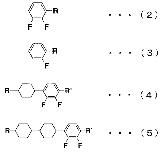
式中、R、R’は、-CnH2n+1(アルキル基)または-O-CnH2n+1(アルコキシ基)である。
誘電異方性がニュートラルである化合物は、粘度を下げたり低温での液晶性を高めたりするために好適に使用される。このような化合物の例としては、下記構造式(6)が挙げられる。

式中、R、R’は、-CnH2n+1(アルキル基)または-O-CnH2n+1(アルコキシ基)である。
本実施形態の液晶表示装置6において、液晶組成物のダイレクタは、電圧無印加時に第1基板71および第2基板72に対してほぼ垂直である。なお、本実施形態において、「液晶組成物のダイレクタが基板に対してほぼ垂直である」との表現は、液晶組成物のダイレクタが基板に鉛直な方向に対して一定の傾斜(プレチルト角)を有する状態で配列していることを含む。液晶組成物のダイレクタは、電圧無印加時に基板に鉛直な方向との間で0.5°以上、5°以下でプレチルトした状態で配列し得る。すなわち、本実施形態の液晶パネル7は、VA方式が採用されている。
・バックライトユニット8
バックライトユニット8は、光を出射するための部位である。バックライトユニット8は、光源81と、光源81からの光を集光して第1基板71へ出光するための光集光部材82を好適に含む。
バックライトユニット8は、光を出射するための部位である。バックライトユニット8は、光源81と、光源81からの光を集光して第1基板71へ出光するための光集光部材82を好適に含む。
光源81は液晶パネル7到達時に光の射出方向を制御して指向性を持たせられるバックライトであればよい。一例として、光源81は、白色LED(Light Emitting Diode)である。光源81は、赤、青、緑色のLEDが用いられてもよい。
光集光部材82は特に限定されない。一例を挙げると、光集光部材82は、導光板、マイクロレンズシート、プリズムシート、ルーバーフィルム等である。
バックライトユニット8の方式は特に限定されない。方式は、直下型方式であってもよく、エッジライト型方式であってもよい。
液晶表示装置6全体の説明に戻り、本実施形態の液晶表示装置6によれば、バックライトユニット8から出射された光は、液晶パネル7の背面71aから液晶パネル7に入り、その後、液晶パネルのおもて面72aから出光され、次いで、光拡散部材1の拡散層5の光拡散部51に入る。その後、光は、光拡散部51のテーパー面53において全反射されて拡散され、次いで散乱層4に受容される。光は、散乱層4において、その多くが前方散乱され、次いで基材2のおもて面21から出光される。このように、本実施形態の液晶表示装置6は、VA方式が採用された液晶パネル7を備えるにもかかわらず、光が良好に散乱される。そのため、液晶表示装置6は、優れた輝度視野角を達成し得る。また、散乱層4において後方散乱が低減されているため、液晶表示装置6は、これら視野角に加え、優れた明所コントラスト比も達成し得る。
<液晶表示装置の製造方法>
上記した実施形態の液晶表示装置を製造する方法は特に限定されない。一例を挙げると、液晶表示装置は、第1基板71および第2基板72の間に、液晶組成物を注入して液晶層73を作製し、次いで、得られた液晶パネル7に、光拡散部材1と、バックライトユニット8とを従来公知の方法によって取り付け、作製し得る。
上記した実施形態の液晶表示装置を製造する方法は特に限定されない。一例を挙げると、液晶表示装置は、第1基板71および第2基板72の間に、液晶組成物を注入して液晶層73を作製し、次いで、得られた液晶パネル7に、光拡散部材1と、バックライトユニット8とを従来公知の方法によって取り付け、作製し得る。
以上、本発明の一実施形態について説明した。本発明は、上記実施形態に限定されない。なお、上記した実施形態は、以下の構成を有する発明の一実施形態である。
(1)互いに対向する第1面および第2面を有する基材と、前記基材の前記第2面の所定領域に積層された第1層と、前記第2面の前記第1層を除く領域に積層された第2層と、前記第2層に積層された第3層と、を備え、前記第3層は、前記第2層との界面から前記第3層の表面にわたって延び、第1材料からなる第1部と、前記第1部を除く領域を占め、第2材料からなる第2部と、が形成されており、前記第2層および前記第3層の、前記第1面に垂直な断面形状は、前記基材から離れる向きに沿って広がるテーパー形状であり、前記第1材料は、前記第2材料よりも屈折率が大きく、前記第2層は、複数の光散乱粒子が分散されたバインダー樹脂からなり、前記第3層におけるテーパー角は、20°以下である、光拡散部材。
このような構成によれば、第3層が受容した光は、第1部において全反射によって拡散され、その後、第2層に向かって進む。第2層において、光は、散乱され、その後、基材の第1面から出光される。第2層において、光は概ね前方へ散乱しており、後方への散乱が低減されている。その結果、光拡散部材は、たとえば液晶表示装置に採用された場合に、視野角(色視野角および輝度視野角)に加え、優れた明所コントラスト比を示し、これらのすべてを達成することができる。特に、光拡散部材は、第2層にもテーパー面が形成されている。そのため、光は、第3層だけでなく、第2層においても拡散される。その結果、光拡散部材は、より優れた視野角および輝度を達成し得る。
(2)前記光散乱粒子の平均粒径は、0.5~5μmである、(1)記載の光拡散部材。
このような構成によれば、光散乱粒子は、第2層において入光を特に前方に散乱させやすい。その結果、得られる光拡散部材は、全光線透過率がさらに向上しやすく、後方散乱が低減しやすい。したがって、光拡散部材は、たとえば液晶表示装置に適用される場合において、明所コントラスト比を維持しつつ、視野角(特に輝度視野角)を向上させやすい。
(3)前記光散乱粒子の濃度は、前記バインダー樹脂中、5~50体積%である、(1)または(2)記載の光拡散部材。
このような構成によれば、光散乱粒子は、第2層において入光を特に前方に散乱させやすい。その結果、得られる光拡散部材は、全光線透過率がさらに向上しやすく、後方散乱が低減しやすい。したがって光拡散部材は、たとえば液晶表示装置に適用される場合において、明所コントラスト比を維持しつつ、視野角(特に輝度視野角)を向上させやすい。
(4)(1)~(3)のいずれかに記載の光拡散部材と、対向して貼り合せられた第1基板および第2基板と、これらの間に保持され、液晶組成物を含む液晶層と、を備えた表示パネルと、光源を備える光源部と、を備え、前記液晶組成物のダイレクタは、電圧無印加時に前記第1基板および前記第2基板に対してほぼ垂直であり、前記光源部は、光源からの光を集光して前記第1基板へ向けて出光する光集光部材を備え、前記第2基板は、前記光拡散部材の前記第3層と接触している、液晶表示装置。
このような構成によれば、光源部から出射されて光拡散部材の第3層が受容した光は、第1部において全反射によって拡散され、その後、第2層に向かって進む。第2層において、光は、散乱され、その後、基材の第1面から出光される。その結果、液晶表示装置は、VA方式において、明所コントラスト比を維持しつつ、優れた暗所コントラスト比と視野角(色視野角および輝度視野角)を示し、これらのすべてを達成することができる。
1 光拡散部材
2 基材
21 おもて面(第1面)
22 背面(第2面)
3 遮光層
4 散乱層
41 バインダー樹脂
42 光散乱粒子
5 拡散層
51 光拡散部
52 テーパー部
6 液晶表示装置
7 液晶パネル
71 第1基板
72 第2基板
73 液晶層
8 バックライトユニット
81 光源
82 光集光部材
2 基材
21 おもて面(第1面)
22 背面(第2面)
3 遮光層
4 散乱層
41 バインダー樹脂
42 光散乱粒子
5 拡散層
51 光拡散部
52 テーパー部
6 液晶表示装置
7 液晶パネル
71 第1基板
72 第2基板
73 液晶層
8 バックライトユニット
81 光源
82 光集光部材
Claims (4)
- 互いに対向する第1面および第2面を有する基材と、
前記基材の前記第2面の所定領域に積層された第1層と、
前記第2面の前記第1層を除く領域に積層された第2層と、
前記第2層に積層された第3層と、を備え、
前記第3層は、
前記第2層との界面から前記第3層の表面にわたって延び、第1材料からなる第1部と、
前記第1部を除く領域を占め、第2材料からなる第2部と、が形成されており、
前記第2層および前記第3層の、前記第1面に垂直な断面形状は、前記基材から離れる向きに沿って広がるテーパー形状であり、
前記第1材料は、前記第2材料よりも屈折率が大きく、
前記第2層は、複数の光散乱粒子が分散されたバインダー樹脂からなり、
前記第3層におけるテーパー角は、20°以下である、光拡散部材。 - 前記光散乱粒子の平均粒径は、0.5~5μmである、請求項1記載の光拡散部材。
- 前記光散乱粒子の濃度は、前記バインダー樹脂中、5~50体積%である、請求項1または2記載の光拡散部材。
- 請求項1~3のいずれか1項に記載の光拡散部材と、
対向して貼り合せられた第1基板および第2基板と、これらの間に保持され、液晶組成物を含む液晶層と、を備えた表示パネルと、
光源を備える光源部と、を備え、
前記液晶組成物のダイレクタは、電圧無印加時に前記第1基板および前記第2基板に対してほぼ垂直であり、
前記光源部は、光源からの光を集光して前記第1基板へ向けて出光する光集光部材を備え、
前記第2基板は、前記光拡散部材の前記第3層と接触している、液晶表示装置。
Priority Applications (1)
| Application Number | Priority Date | Filing Date | Title |
|---|---|---|---|
| PCT/JP2018/039893 WO2020084768A1 (ja) | 2018-10-26 | 2018-10-26 | 光拡散部材および液晶表示装置 |
Applications Claiming Priority (1)
| Application Number | Priority Date | Filing Date | Title |
|---|---|---|---|
| PCT/JP2018/039893 WO2020084768A1 (ja) | 2018-10-26 | 2018-10-26 | 光拡散部材および液晶表示装置 |
Publications (1)
| Publication Number | Publication Date |
|---|---|
| WO2020084768A1 true WO2020084768A1 (ja) | 2020-04-30 |
Family
ID=70331466
Family Applications (1)
| Application Number | Title | Priority Date | Filing Date |
|---|---|---|---|
| PCT/JP2018/039893 Ceased WO2020084768A1 (ja) | 2018-10-26 | 2018-10-26 | 光拡散部材および液晶表示装置 |
Country Status (1)
| Country | Link |
|---|---|
| WO (1) | WO2020084768A1 (ja) |
Citations (2)
| Publication number | Priority date | Publication date | Assignee | Title |
|---|---|---|---|---|
| WO2012081410A1 (ja) * | 2010-12-14 | 2012-06-21 | シャープ株式会社 | 光拡散部材およびその製造方法、表示装置 |
| WO2012157511A1 (ja) * | 2011-05-13 | 2012-11-22 | シャープ株式会社 | 光拡散部材およびその製造方法、表示装置 |
-
2018
- 2018-10-26 WO PCT/JP2018/039893 patent/WO2020084768A1/ja not_active Ceased
Patent Citations (2)
| Publication number | Priority date | Publication date | Assignee | Title |
|---|---|---|---|---|
| WO2012081410A1 (ja) * | 2010-12-14 | 2012-06-21 | シャープ株式会社 | 光拡散部材およびその製造方法、表示装置 |
| WO2012157511A1 (ja) * | 2011-05-13 | 2012-11-22 | シャープ株式会社 | 光拡散部材およびその製造方法、表示装置 |
Similar Documents
| Publication | Publication Date | Title |
|---|---|---|
| TWI463201B (zh) | 較高傳輸之光控制薄膜 | |
| CN202614963U (zh) | 光扩散部件和显示装置 | |
| CN104204922B (zh) | 液晶显示装置 | |
| US8390764B2 (en) | Composite polarizing plate having a light diffusion pressure-sensitive adhesion layer and liquid crystal display device | |
| CN202661658U (zh) | 光扩散部件和显示装置 | |
| CN103907053B (zh) | 液晶显示装置 | |
| WO2012157517A1 (ja) | 光拡散部材およびその製造方法、表示装置 | |
| TWI485466B (zh) | 液晶顯示裝置 | |
| CN101300521A (zh) | 液晶显示装置 | |
| US7722240B2 (en) | Surface light source device and transmission display device | |
| US20180128959A1 (en) | Optical sheet, image source unit and image display device | |
| JP2016038593A (ja) | 映像源ユニット、及び表示装置 | |
| JP5860142B2 (ja) | 光制御部材およびその製造方法、表示装置 | |
| JP2017198735A (ja) | 光学シート、映像源ユニット及び液晶表示装置 | |
| WO2014092017A1 (ja) | 光拡散部材及び表示装置 | |
| US11635562B2 (en) | Image source unit, and liquid crystal display device | |
| JP2005055620A (ja) | 反射型表示素子 | |
| JP2013222157A (ja) | 光拡散部材および表示装置 | |
| JP2017120714A (ja) | 面光源装置、映像源ユニット、及び表示装置 | |
| JP7135294B2 (ja) | 光学シート、面光源装置、映像源ユニット、及び表示装置 | |
| JP2018136423A (ja) | 光学シート、面光源装置、映像源ユニット、及び表示装置 | |
| JP2017198974A (ja) | 光学ユニット、面光源装置、映像源ユニット、及び液晶表示装置 | |
| JP2019060904A (ja) | 光学シート、面光源装置、映像源ユニット、及び表示装置 | |
| JP2014021147A (ja) | 光拡散部材、光拡散部材の製造方法、及び表示装置 | |
| WO2020194719A1 (ja) | 液晶表示装置 |
Legal Events
| Date | Code | Title | Description |
|---|---|---|---|
| 121 | Ep: the epo has been informed by wipo that ep was designated in this application |
Ref document number: 18937859 Country of ref document: EP Kind code of ref document: A1 |
|
| NENP | Non-entry into the national phase |
Ref country code: DE |
|
| 122 | Ep: pct application non-entry in european phase |
Ref document number: 18937859 Country of ref document: EP Kind code of ref document: A1 |
|
| NENP | Non-entry into the national phase |
Ref country code: JP |