WO2020035904A1 - 電磁波受信機及びレーダ装置 - Google Patents
電磁波受信機及びレーダ装置 Download PDFInfo
- Publication number
- WO2020035904A1 WO2020035904A1 PCT/JP2018/030283 JP2018030283W WO2020035904A1 WO 2020035904 A1 WO2020035904 A1 WO 2020035904A1 JP 2018030283 W JP2018030283 W JP 2018030283W WO 2020035904 A1 WO2020035904 A1 WO 2020035904A1
- Authority
- WO
- WIPO (PCT)
- Prior art keywords
- electromagnetic wave
- unit
- cavity
- resonance
- current
- Prior art date
- Legal status (The legal status is an assumption and is not a legal conclusion. Google has not performed a legal analysis and makes no representation as to the accuracy of the status listed.)
- Ceased
Links
Images













Classifications
-
- G—PHYSICS
- G01—MEASURING; TESTING
- G01J—MEASUREMENT OF INTENSITY, VELOCITY, SPECTRAL CONTENT, POLARISATION, PHASE OR PULSE CHARACTERISTICS OF INFRARED, VISIBLE OR ULTRAVIOLET LIGHT; COLORIMETRY; RADIATION PYROMETRY
- G01J1/00—Photometry, e.g. photographic exposure meter
- G01J1/02—Details
-
- G—PHYSICS
- G01—MEASURING; TESTING
- G01S—RADIO DIRECTION-FINDING; RADIO NAVIGATION; DETERMINING DISTANCE OR VELOCITY BY USE OF RADIO WAVES; LOCATING OR PRESENCE-DETECTING BY USE OF THE REFLECTION OR RERADIATION OF RADIO WAVES; ANALOGOUS ARRANGEMENTS USING OTHER WAVES
- G01S7/00—Details of systems according to groups G01S13/00, G01S15/00, G01S17/00
- G01S7/02—Details of systems according to groups G01S13/00, G01S15/00, G01S17/00 of systems according to group G01S13/00
- G01S7/28—Details of pulse systems
- G01S7/285—Receivers
-
- G—PHYSICS
- G01—MEASURING; TESTING
- G01S—RADIO DIRECTION-FINDING; RADIO NAVIGATION; DETERMINING DISTANCE OR VELOCITY BY USE OF RADIO WAVES; LOCATING OR PRESENCE-DETECTING BY USE OF THE REFLECTION OR RERADIATION OF RADIO WAVES; ANALOGOUS ARRANGEMENTS USING OTHER WAVES
- G01S7/00—Details of systems according to groups G01S13/00, G01S15/00, G01S17/00
- G01S7/48—Details of systems according to groups G01S13/00, G01S15/00, G01S17/00 of systems according to group G01S17/00
- G01S7/483—Details of pulse systems
- G01S7/486—Receivers
-
- H—ELECTRICITY
- H01—ELECTRIC ELEMENTS
- H01P—WAVEGUIDES; RESONATORS, LINES, OR OTHER DEVICES OF THE WAVEGUIDE TYPE
- H01P7/00—Resonators of the waveguide type
- H01P7/06—Cavity resonators
Definitions
- the present invention relates to an electromagnetic wave receiver and a radar device.
- Patent Document 1 discloses a receiver for an electromagnetic wave having a frequency within a frequency range of 0.1 to 10 terahertz (THz), that is, a so-called “terahertz wave”.
- the receiver described in Patent Document 1 amplifies an electric signal corresponding to the input electromagnetic wave by using an FET (Field Effect Transistor) when an electromagnetic wave is input to the antenna.
- FET Field Effect Transistor
- the receiver described in Patent Literature 1 has a problem that the receiving sensitivity to electromagnetic waves having a frequency of 10 THz or more is low. That is, the receiver described in Patent Document 1 has a problem that it cannot be used for receiving electromagnetic waves having a frequency of 10 THz or more.
- the present invention has been made to solve the above-described problems, and has as its object to provide an electromagnetic wave receiver having high reception sensitivity over a wide frequency range. It is another object of the present invention to provide a radar device using the electromagnetic wave receiver.
- the electromagnetic wave receiver of the present invention uses an electromagnetic wave receiving unit that receives an input electromagnetic wave, and the behavior of a current flowing through the electromagnetic wave receiving unit or a voltage to be applied, so that a lower frequency than a DC electric signal or an input electromagnetic wave is used.
- a signal generation unit that generates an electric signal of the electromagnetic wave receiver, wherein the electromagnetic wave reception unit is a cavity having an electromagnetic wave input unit that inputs an electromagnetic wave, and a plurality of resonance cavities provided in a conductor plate or a conductor layer.
- the radar device of the present invention includes the electromagnetic wave receiver.
- an electromagnetic wave receiver having a high reception sensitivity over a wide frequency range can be obtained because of the configuration described above. Further, a radar device using this electromagnetic wave receiver can be obtained.
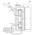
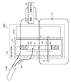
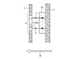
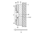
- FIG. 2 is an explanatory diagram illustrating a state where a main part of the electromagnetic wave receiver according to Embodiment 1 is viewed from a cross section.
- FIG. 3 is an explanatory diagram showing a state where a part including the cavity resonance part in the electromagnetic wave receiver according to Embodiment 1 is viewed from the front.
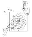
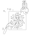
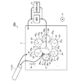
- FIG. 3 is an explanatory diagram showing directions and the like of various currents in a first half cycle in the electromagnetic wave receiver according to Embodiment 1.
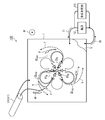
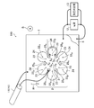
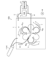
- FIG. 3 is an explanatory diagram showing directions of various currents and the like in a second half cycle in the electromagnetic wave receiver according to Embodiment 1.
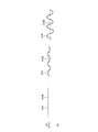
- FIG. 3A is a timing chart showing a voltage value corresponding to an electromagnetic wave input to the electromagnetic wave input unit and a current value corresponding to the electromagnetic wave.
- FIG. 3B is a timing diagram showing the value of the potential at each first electrode, the value of the current at each first electrode, and the value of the bias voltage at each first diode.
- FIG. 3C is a timing chart showing the potential values at the individual second electrodes, the current values at the individual second electrodes, and the bias voltage values at the individual second diodes.
- FIG. 3D is a timing chart showing values of a current flowing from the first electrode to the second electrode.
- FIG. 3E is a timing chart showing values of a current flowing from the second electrode to the first electrode.
- FIG. 3F is a timing chart showing the value of the potential difference between the first electrode and the second electrode.
- FIG. 3G is a timing chart showing the value of the reception current and the average value of the reception current.
- FIG. 3 is a characteristic diagram showing voltage-current characteristics of individual diodes.
- FIG. 4 is an explanatory diagram showing a time change of a value of an applied voltage in each diode and a time change of a value of a bias voltage in each diode. It is explanatory drawing which shows the time change of the value of the conduction current in each diode, and the time change of the average value of the conduction current in each diode.
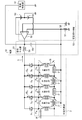
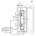
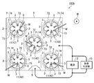
- the electromagnetic wave receiver according to the first embodiment in the circuit diagram obtained by combining the circuit diagram showing the equivalent circuit of the electromagnetic wave generation unit and the circuit diagram showing the internal configuration of the power supply, the direction of various currents in the second half cycle, etc.
- FIG. In the electromagnetic wave receiver according to Embodiment 1, in the circuit diagram combining the circuit diagram showing the equivalent circuit of the electromagnetic wave generator and the circuit diagram showing the other internal configuration of the power supply, the circuit diagram of FIG. It is explanatory drawing which shows a direction etc.
- the circuit diagram of FIG. in the circuit diagram combining the circuit diagram showing the equivalent circuit of the electromagnetic wave generation unit and the circuit diagram showing the other internal configuration of the power supply, the circuit diagram of FIG. It is explanatory drawing which shows a direction etc.
- FIG. 5 is an explanatory diagram showing a state where a main part of another electromagnetic wave receiver according to Embodiment 1 is viewed from a cross section.
- FIG. 4 is an explanatory diagram showing a state where a portion including a cavity resonance portion in another electromagnetic wave receiver according to Embodiment 1 is viewed from the front.
- the circuit diagram of FIG. It is explanatory drawing which shows a direction etc.
- FIG. 5 is an explanatory diagram showing a state where a main part of another electromagnetic wave receiver according to Embodiment 1 is viewed from a cross section.
- FIG. 4 is an explanatory diagram showing a state where a portion including a cavity resonance portion in another electromagnetic wave receiver according to Embodiment 1 is viewed from the front.
- FIG. 5 is an explanatory diagram showing a state where a main part of another electromagnetic wave receiver according to Embodiment 1 is viewed from a cross section.
- FIG. 4 is an explanatory diagram showing a state where a portion including a cavity resonance portion in another electromagnetic wave receiver according to Embodiment 1 is viewed from the front.
- FIG. 4 is an explanatory diagram showing another electromagnetic wave input unit in the electromagnetic wave receiver according to Embodiment 1.
- FIG. 4 is an explanatory diagram showing another electromagnetic wave input unit in the electromagnetic wave receiver according to Embodiment 1.
- FIG. 4 is an explanatory diagram showing another electromagnetic wave input unit in the electromagnetic wave receiver according to Embodiment 1.
- FIG. 4 is an explanatory diagram showing another electromagnetic wave input unit in the electromagnetic wave receiver according to Embodiment 1.
- FIG. 4 is an explanatory diagram illustrating a main part of another electromagnetic wave receiver according to Embodiment 1.
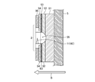
- FIG. 7 is an explanatory diagram showing a state where a main part of the electromagnetic wave receiver according to Embodiment 2 is viewed from a cross section.
- FIG. 11 is an explanatory diagram showing a state where a part including a cavity resonance part in the electromagnetic wave receiver according to Embodiment 2 is viewed from the front.
- FIG. 9 is an explanatory diagram showing directions and the like of various currents in a first half cycle in the electromagnetic wave receiver according to Embodiment 2.
- FIG. 9 is an explanatory diagram showing directions and the like of various currents in a second half cycle in the electromagnetic wave receiver according to Embodiment 2.
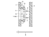
- FIG. 9 is an explanatory diagram showing a state where a main part of the electromagnetic wave receiver according to Embodiment 3 is viewed from a cross section.
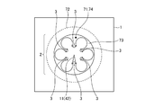
- FIG. 13 is an explanatory diagram showing a state where a portion including a plurality of cavity resonance portions in the electromagnetic wave receiver according to Embodiment 3 is viewed from the front.
- FIG. 10 is an explanatory diagram showing a state where a portion including individual cavity resonance portions in the electromagnetic wave receiver according to Embodiment 3 is viewed from a cross section.
- FIG. 13 is an explanatory diagram showing a state where a portion including individual cavity resonance portions in the electromagnetic wave receiver according to Embodiment 3 is viewed from the front.
- FIG. 14 is an explanatory diagram illustrating another current limiting unit in the electromagnetic wave receiver according to Embodiment 3.
- FIG. 14 is an explanatory diagram illustrating another current limiting unit in the electromagnetic wave receiver according to Embodiment 3.
- FIG. 14 is an explanatory diagram illustrating another current limiting unit in the electromagnetic wave receiver according to Embodiment 3.
- FIG. 14 is an explanatory diagram illustrating another current limiting unit in the electromagnetic wave receiver according to Embodiment 3.
- FIG. 14 is an explanatory diagram illustrating another current limiting unit in the electromagnetic wave receiver according to Embodiment 3.
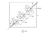
- FIG. 9 is an explanatory diagram illustrating an example of directivity when a plurality of cavity resonators are regularly arranged.
- FIG. 9 is an explanatory diagram showing another example of directivity when a plurality of cavity resonators are regularly arranged.
- FIG. 9 is an explanatory diagram showing another example of directivity when a plurality of cavity resonators are regularly arranged.
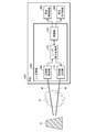
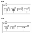
- FIG. 14 is a block diagram showing a main part of a radar device according to Embodiment 4.
- FIG. 27A is a block diagram illustrating a hardware configuration of a radar device according to Embodiment 4.
- FIG. 27B is a block diagram illustrating another hardware configuration of the radar apparatus according to Embodiment 4.
- FIG. 1A is an explanatory diagram showing a state where a main part of the electromagnetic wave receiver according to Embodiment 1 is viewed from a cross section.
- FIG. 1B is an explanatory diagram showing a state where a part including the cavity resonance part in the electromagnetic wave receiver according to Embodiment 1 is viewed from the front.
- an electromagnetic wave receiver 100 according to Embodiment 1 will be described.
- a cavity plate 2 is provided on a conductor plate 1. More specifically, one substantially circular through-hole 21 is formed in the conductor plate 1, and a plurality (N) of substantially circular shapes arranged in an annular shape around the through-hole 21. Are formed in the conductor plate 1.
- Each through hole 22 has an opening 23 to the through hole 21 and communicates with the through hole 21.
- the creepage length L1 of the wall portion 24 of each through hole 22 is set to a value that is ⁇ times the wavelength ⁇ of the electromagnetic wave W received by the electromagnetic wave receiver 100.
- Resonant cavities 22 are formed by the individual through holes 22.
- the through hole 22 may be described as a resonance cavity 22.
- the individual electrodes 25 are formed by the conductor between each two adjacent resonance cavities 22, that is, by the portion of the conductor plate 1 between each two adjacent resonance cavities 22. Therefore, the number of the electrodes 25 is the same as the number of the resonance cavities 22, and the cavity resonance section 2 has N resonance cavities 22 and N electrodes 25.
- the tips of the two electrodes 25 arranged to face each other via the opening 23 function as a capacitor, and the substantially annular wall portion 24 functions as a coil by the so-called "skin effect".
- the anodes of the N diodes 3 are electrically connected to the tips of the N electrodes 25, respectively.
- the cathodes of the N diodes 3 are electrically connected to the substrate 5 via the conductor bar 4.
- Each of the diodes 3 is composed of, for example, a PN junction diode, a Schottky barrier diode, a PIN diode, or the like.
- the substrate 5 has conductivity and is arranged inside the container 6 so as to face the conductor plate 1.
- a gap 8 is formed between the substrate 5 and the conductive plate 1 by the insulating member 7 provided between the substrate 5 and the conductive plate 1.
- N pieces of the resonant cavity 22 is convenient N / 2 pieces of the resonant cavity (hereinafter sometimes referred to as “first resonant cavity”.) 22 A and residual N / 2 pieces of the resonant cavity (hereinafter “ sometimes referred to as a second resonant cavity “.) 22 and B are those which are alternately arranged.
- the N electrodes 25 include, for convenience, N / 2 electrodes (hereinafter may be referred to as “first electrodes”) 25 A and the remaining N / 2 electrodes (hereinafter referred to as “second electrodes”). And B are alternately arranged.
- the N diodes 3 are conveniently N / 2 diodes (hereinafter sometimes referred to as “first diode”) 3 A and the remaining N / 2 diodes (hereinafter referred to as “second diode”). there.) in which 3 and B are arranged alternately.
- the container 6 need not be a sealed container.
- a magnetic field applying unit 9 is provided outside the container 6 on one side of the conductor plate 1 (that is, on one side of the substrate 5).
- the magnetic field applying unit 9 is configured by a permanent magnet 31.
- the magnetic field application unit 9 applies a magnetic field B that generates a magnetic flux in a direction perpendicular to the plate surface of the conductor plate 1 (that is, the plate surface of the substrate 5) to the cavity resonance unit 2.
- the conductor plate 1, the cavity resonator 2, the diode 3, the conductor rod 4, the substrate 5, the container 6, the insulating member 7, and the magnetic field applying unit 9 constitute a main part of the electromagnetic wave receiving unit 10.
- An electromagnetic wave input unit 11 is provided outside the container 6.
- the electromagnetic wave input unit 11 inputs an electromagnetic wave W.
- the electromagnetic wave input unit 11 includes a transmission line 41 for the electromagnetic wave W.
- the transmission line 41 is composed of, for example, a coaxial cable or a waveguide.
- ⁇ ⁇ It is necessary to use a member corresponding to the wavelength ⁇ of the electromagnetic wave W for the connection line between the electromagnetic wave input unit 11 and the cavity resonance unit 2.
- the electromagnetic wave W is visible light
- a material that transmits visible light such as transparent glass, transparent ceramics or transparent resin
- the electromagnetic wave W is infrared light
- a material that transmits infrared light it is necessary to use a material that transmits infrared light for the connection line.
- a power supply 12 is provided outside the container 6. One terminal of the power supply 12 is electrically connected to the conductor plate 1, and the other terminal of the power supply 12 is electrically connected to the substrate 5. As a result, the cathodes of the N diodes 3 are electrically connected to the power supply 12 via the conductor bar 4 and the substrate 5.
- the power supply 12 supplies a current for amplification by the cavity resonance unit 2 (hereinafter referred to as “amplification current”) and applies a bias voltage to the diode 3.
- the electromagnetic wave receiving unit 10 receives the electromagnetic wave W input to the electromagnetic wave input unit 11. More specifically, the electromagnetic wave receiving unit 10 amplifies the current corresponding to the electromagnetic wave W using the amplification current. This amplifying operation is performed by the cavity resonator 2, and the N diodes 3 perform a function of supplying an amplification current to the cavity resonator 2. The details of the amplifying operation of the cavity resonator 2 will be described later with reference to FIGS.
- a portion that functions to supply an amplification current to the cavity resonance section 2 is referred to as a “current supply section”.
- a reception determination unit 13 is provided outside the container 6. The reception determination unit 13 determines whether or not the electromagnetic wave W is received by the electromagnetic wave reception unit 10 based on the behavior of the current supplied from the power supply 12 and flowing through the electromagnetic wave reception unit 10 or the applied voltage.
- the electromagnetic wave receiving unit 10, the electromagnetic wave input unit 11, the power supply 12, and the reception determining unit 13 constitute a main part of the electromagnetic wave receiver 100.
- the cavity resonance unit 2 can amplify the electromagnetic wave W having an arbitrary frequency f according to the size (size) of each resonance cavity 22, more specifically, according to the value of the creeping length L1. Therefore, the electromagnetic wave receiver 100 can adjust the dimensions of the individual resonance cavities 22, more specifically, adjust the value of the creepage length L ⁇ b> 1, and use the same for receiving the electromagnetic wave W having an arbitrary frequency f. it can.
- the creepage length L1 when the creepage length L1 is set to 300 micrometers ( ⁇ m), an electromagnetic wave having a frequency f of 1 THz can be amplified. Therefore, the electromagnetic wave W having the frequency f of 1 THz can be received.
- the creepage length L1 is set to 0.3 ⁇ m, an electromagnetic wave having a frequency f of 1000 THz is amplified. Therefore, the electromagnetic wave W having the frequency f of 1000 THz can be received.
- the electromagnetic wave W having the frequency f within the frequency range of 1 to 1000 THz hereinafter referred to as “terahertz range” is received. be able to.
- Electromagnetic waves W having a frequency f in the terahertz range are being applied to various technical fields.
- applications in technical fields such as a fluoroscope for a human body, a radar device for a vehicle, identification of biomolecules, evaluation of physical properties of electronic materials, nondestructive measurement, and medical equipment have been promoted. Therefore, the electromagnetic wave receiver 100 can be applied to these technical fields.
- the creepage length L1 when the creepage length L1 is set to a value larger than 300 ⁇ m, the electromagnetic wave having the frequency f lower than 1 THz is amplified. Therefore, it is possible to receive the electromagnetic wave W having the frequency f lower than 1 THz. As described above, by setting the creepage length L1 to a value larger than 300 ⁇ m, it is also possible to receive an electromagnetic wave W having a frequency f in a frequency region lower than the terahertz region.
- the corresponding electromagnetic wave W is far infrared rays.
- the corresponding electromagnetic wave W becomes visible light.
- the corresponding electromagnetic wave W is yellow visible light.
- the electromagnetic wave receiver 100 can be used for receiving light.
- the size of the cavity resonator 2 is on the order of micrometers or nanometers.
- the conductor plate 1 having such a minute cavity resonance portion 2 is manufactured using, for example, a so-called “3D printer”. Alternatively, it is manufactured using, for example, a microfabrication technique (plating, vapor deposition, deposition, etching, or the like) for forming a conductor pattern in an IC (Integrated Circuit). Alternatively, for example, it is manufactured using a microfabrication technique for a conductive material in a so-called “metamaterial”.
- the magnetic field B for generating a magnetic flux in a direction perpendicular to the plate surface can be applied using the permanent magnet 31 provided on one side of the conductor plate 1.
- the magnetic field applying unit 9 is provided outside the container 6. However, in order to effectively apply a magnetic field, the magnetic field applying unit 9 may be provided inside the container 6 and approach the conductor plate 1. .
- the size of each of the resonance cavities 22 becomes large, and the size of the cavity resonance portion 2 may become larger than that of the above specific example. Further, when it is required to further improve the receiving sensitivity, the number of the resonance cavities 22 may increase, and the size of the cavity resonance unit 2 may be larger than that of the above specific example. This may make it difficult to apply a magnetic field B that generates a magnetic flux in a direction perpendicular to the plate surface only with the permanent magnet 31 arranged on one side of the conductor plate 1 alone.
- the magnetic field applying unit 9 may be configured by two magnets, and the container 6 may be arranged between the two magnets.
- the operation of the electromagnetic wave receiver 100 will be described with reference to FIGS. Note that, in FIG. 2, the reference numerals of the cavity resonance unit 2, the reference numerals of the diode 3, and the reference numerals of the conductor rods 4 are omitted. Further, the reference numerals of the respective parts in the cavity resonance section 2 are also omitted from the drawing.
- I1 in FIG. 2 indicates the direction of the current supplied by the power supply 12, that is, the direction of the amplification current.
- I2 (I2 AB and I2 BA) in FIG. 2 the current flowing through the cavity portion 2, more specifically (sometimes hereinafter referred to as "resonant current”.)
- the current flowing in each of the resonant cavity 22 indicates the direction of ing.
- I3 (I3 A and I3 B) in FIG. 2 shows the direction of the current flowing through the individual diodes 3 (hereinafter sometimes referred to as "energization current”.).
- I1 also indicates the direction of the current flowing through the electromagnetic wave receiving unit 10, that is, the current flowing through the cavity resonance unit 2 (hereinafter, sometimes referred to as "reception current").
- the clockwise direction in FIG. 2 is simply referred to as “clockwise direction”
- the counterclockwise direction in FIG. 2 is simply referred to as “counterclockwise direction”.
- each resonance cavity 22 functions as an LC resonance circuit.
- first half cycle the first half cycle (hereinafter, referred to as “first half cycle”) of each resonance cycle is formed along the wall portion 24 of each resonance cavity 22.
- the second half period Te toward the second electrode 25 B from the first electrode 25 a current I2 with BA flows, the second half period (hereinafter referred to as "the second half-period.") at the first electrode 25 from the a second of the resonance period a state in which current I2 AB towards the electrode 25 B flows. That is, in each wall portion 24 of each resonance cavity 22, a clockwise current I2 and a counterclockwise current I2 along the wall portion 24 alternately flow in the same wall portion 24. .
- the current for amplification supplied from the power supply 12 is supplied to the cavity resonator 2 via the diode 3.
- This amplification current also behaves as described above (that is, a force F in the counterclockwise direction is applied by the magnetic field B to the electrons of the amplification current moving in the conductor of the cavity resonator 2, and the amplification current Therefore, in each of the first and second half periods, the amplification current flows in the same direction as the resonance current on the wall portion 24.
- the amplification current flows in the same direction at the same timing as the resonance current, the amplification current is added to the resonance current flowing through the wall surface portion 24.
- the magnetic energy of the amplified current corresponding to a current obtained by addition is stored in the respective first resonant cavity 22 A to the resonant current, then the stored magnetic energy by resonance operation Converted to charge energy.
- Amplifying current at this time flows a current I3 A to the first diode 3 A.
- the second half period by which the converted charge energy flows out into individual second resonant cavity 22 B by the resonant operation, the resonant current flows through the respective second resonant cavity 22 B.
- the behavior of the tip of the electrode 25 will be described.
- the potentials of the individual electrodes 25 also vibrate.
- the potential of the first electrode 25 A and the potential of the high state than the potential of the second electrode 25 B second electrode 25 B is alternately repeated and high state than the potential of the first electrode 25 A It is.
- the potential of the second electrode 25 B has a low state than the potential of the low state than the potential of the first electrode 25 A first electrode 25 A and the second electrode 25 B is alternately Is repeated.
- the anodes of the N diodes 3 are electrically connected to the tips of the N electrodes 25, respectively.
- Voltage having the diode 3 - by the current characteristics in the potential of the first electrode 25 A is high relative to the potential of the second electrode 25 B, while the current I3 A flows through the first diode 3 A, a second diode 3 hardly flows current I3 B to B (see FIG. 2A).
- the potential of the second electrode 25 B is in a high state than the potential of the first electrode 25 A, while the current flows I3 B to the second diode 3 B, the first diode 3 A current I3 A It hardly flows (see FIG. 2B).
- the amplification current flowing through the electrode 25 to be added with the amplification current of the N electrodes 25 (that is, the electrode 25 on the high potential side at each time) can be increased, and the remaining electrode 25 can be increased. (That is, the current for amplification flowing to the electrode 25 on the low potential side at each time) can be suppressed.
- the N diodes 3 are provided at the respective tips of the N electrodes 25, the conduction current can be distributed according to the potential of each electrode 25, and the amplification current can be appropriately resonated.
- the power can be supplied to the cavity 22 and further to the cavity resonance unit 2.
- FIG. 3A is a timing chart showing a voltage value (I in the figure) corresponding to the electromagnetic wave W and a current value (II in the figure) corresponding to the electromagnetic wave W.
- Figure 3B the value of the bias voltage in each potential value at the first electrode 25 A (figure III), the value of the current in each of the first electrode 25 A (in the drawing IV) and respective first diode 3 A It is a timing diagram showing (V in the figure). Note that the value of the potential of each of the first electrode 25 A (figure III) are those corresponding to the value of the applied voltage in each of the first diode 3 A. The value of the current in each of the first electrode 25 A (figure IV) are those corresponding to the value of the current flowing in each of the first diode 3 A.
- Figure 3C the value of the bias voltage in each of the second electrode 25 potential values in B (figure VI), the value of the current in each of the second electrodes 25 B (in the drawing VII) and individual second diode 3 B It is a timing diagram showing (VIII in a figure). Note that the value of the potential of each of the second electrodes 25 B (figure VI) are those corresponding to the value of the applied voltage in each of the second diode 3 B. The value of the current in each of the second electrodes 25 B (figure VII) are those corresponding to the value of the current flowing in the respective second diodes 3 B.
- Figure 3D is a timing diagram illustrating the value of the current I2 AB flowing from the first electrode 25 A to the second electrode 25 B (the figure IX).
- Figure 3E is a timing diagram illustrating the value of the current I2 BA flowing from the second electrode 25 B to the first electrode 25 A (the figure X).
- Figure 3F is a timing diagram showing a first electrode 25 A potential difference value between the second electrodes 25 B (the figure XI).
- FIG. 3G is a timing chart showing the value of the received current (XII in the figure) and the average value of the received current (XIII in the figure).
- the value of the received current (XII in the figure) corresponds to the total value of the currents flowing through the N diodes 3.
- the average value of the reception current (XIII in the figure) corresponds to the average value of the sum of the currents flowing through the N diodes 3.
- the average value of the sum of the currents flowing through the N diodes 3 may be referred to as “total average current flowing”. Further, the average value of the energizing current in each diode 3 may be referred to as “individual average energizing current”.
- the bias voltage at each diode 3 gradually decreases. Note that if an excessively large electromagnetic wave W is input, the bias voltage is inverted, but operation of the region is not required for receiving the weak electromagnetic wave W.
- the reason why the total average energizing current is maintained at a constant value despite the fact that the amplitude of the received current gradually increases is that the power supply 12 changes the bias voltage with respect to the diode 3. This is because control for maintaining the total average energizing current at a constant value (hereinafter, referred to as “constant current control”) is performed.
- FIG. 4A shows voltage-current characteristics of the diode 3.
- the diode 3 has a non-linear voltage-current characteristic as shown in FIG. 4A.
- VF forward voltage
- the bias voltage (XXII in the figure) on each diode 3 increases. Is gradually changed from a forward bias (0.7 volts in the drawing) to a direction of decreasing the bias (0 volts in the drawing). More specifically, the bias voltage is reduced so that when the top of the waveform of the applied voltage exceeds the forward voltage VF, the remaining portion of the waveform falls below the forward voltage VF.
- the individual average conduction current (XXIV in the figure) is a constant value equivalent to IF. (For example, 0.1 amps).
- the total average energizing current (not shown) is also kept at a constant value (for example, N times the value of IF).
- the reception determining unit 13 can determine whether the electromagnetic wave W is received by the electromagnetic wave receiving unit 10 based on the value of the voltage applied to the electromagnetic wave receiving unit 10 by the power supply 12.
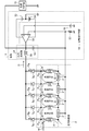
- the constant current control is realized by, for example, the circuit shown in FIG.
- the circuit shown in FIG. 5 is a combination of an equivalent circuit of the electromagnetic wave reception unit 10 and a circuit showing the internal configuration of the power supply 12, and includes a signal generation unit 51 described later.
- the plurality of nodes P in the equivalent circuit of the electromagnetic wave receiving unit 10 correspond to the plurality of electrodes 25, respectively.
- each of the plurality of F's in the equivalent circuit of the electromagnetic wave receiving unit 10 is a circuit element corresponding to the rectifying action by the force F received by the moving electrons in the magnetic field shown in FIG. 2, that is, the clockwise current in FIG. It is a circuit element corresponding to the action of flowing a large amount of I2 BA and I2 AB .
- the power supply 12 includes a signal generation unit 51, a constant current control unit 52, a power supply 53, and a power supply 54.
- the signal generation unit 51 is a filter for obtaining an average value of the reception current I1, that is, a total average conduction current, and includes a capacitor 55 and a coil 56.
- the constant current control unit 52 includes a resistor 57 for current detection, a power supply 58 for generating a reference voltage, and an error amplifier 59, and realizes constant current control by feedback control.
- the filter formed by the capacitor 55 and the coil 56 of the signal generator 51 has a smoothing function. For this reason, when the electromagnetic wave W is a monotone wave (that is, an unmodulated wave), the reception current including the high frequency component passes through the signal generation unit 51 and is converted into a DC signal. DC signals having different levels are detected when the electromagnetic wave W is received and when the electromagnetic wave W is not received, so that when both are alternately repeated, the waveform becomes a rectangular waveform.
- the received current passes through the signal generation unit 51 and is demodulated with a signal having a waveform corresponding to the demodulated wave, that is, a frequency f ′ lower than the frequency f of the electromagnetic wave W. Converted to a signal.
- the signal generation unit 51 generates a DC electric signal or an electric signal having a frequency lower than that of the electromagnetic wave W by using the behavior of the current flowing through the electromagnetic wave receiving unit or the applied voltage.
- the signal generation unit 51 generates a DC electric signal or an electric signal of a lower frequency than the electromagnetic wave W using the behavior of the current flowing through the electromagnetic wave receiving unit or the behavior of the applied voltage.
- the unit 13 can determine whether the electromagnetic wave reception unit 10 has received the electromagnetic wave W based on the voltage waveform at the connection point between the power supply 12 and the signal generation unit 51.
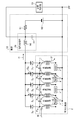
- the power supply 12 includes a signal generator 51, a current limiting resistor 61, and a voltage (for example, 10 volts) sufficiently higher than a forward voltage VF (for example, 0.7 volts) of the diode 3. ) May be used.
- a voltage for example, 10 volts
- VF forward voltage
- the power supply 12 can be realized with a simpler circuit configuration than the example shown in FIG.
- the cathodes of the N diodes 3 are electrically connected to the tips of the N electrodes 25, respectively, and the anodes of the N diodes 3 are connected to the conductor rod 4 and the substrate 5 respectively.
- 1 and FIG. 2 which are electrically connected in common with the power supply 12 via the power supply 12 may be inverted in polarity.
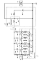
- the circuit shown in FIG. 8 is a combination of an equivalent circuit of the electromagnetic wave receiving unit 10 and a circuit showing the internal configuration of the power supply 12 in this case.
- the polarity of the diode 3 and the power supply 58 for generating the reference voltage in FIG. Has been inverted.
- the anodes of N diodes 3 are electrically connected to the tips of the N electrodes 25, and the cathodes of the N diodes 3 are electrically connected to the power supply 12 via the substrate 5. May be connected in common. In this case, the conductor bar 4 shown in FIG. 1 is unnecessary.
- the circuit diagram in this case is the same as that shown in FIG.
- the cathodes of the N diodes 3 are electrically connected to the tips of the N electrodes 25, respectively, and the anodes of the N diodes 3 are electrically connected to the power supply 12 via the substrate 5.
- the polarity of the diode 3 in FIG. also in this case, the conductor bar 4 shown in FIG. 1 is unnecessary.
- the circuit diagram in this case is the same as that shown in FIG.
- each diode 3 may be provided such that the direction of current is provided along the direction orthogonal to the plate surface of the conductive plate 1.
- the cavity resonating part 2 can be formed on a semiconductor wafer in which the diode 3 is generated by using the IC manufacturing technique, using a metal foil serving as a wiring or an electrode as a conductor plate 1 in a general IC. Therefore, it is possible to easily manufacture the diode 3 and the electromagnetic wave receiving unit 10.
- a lead frame for mounting the diode 3 corresponds to the substrate 5.
- a protrusion 42 whose longitudinal direction is directed to a direction along the plate surface of the conductive plate 1 is provided at a tip portion of any one of the N electrodes 25.
- the electromagnetic wave input section 11 may be constituted by the projections 42.
- the protrusion 42 may be formed integrally with the conductor plate 1, and the protrusion length L2 of the protrusion 42 is set to a value that is 1/4 times the wavelength ⁇ .
- the protrusion 42 functions as an input antenna for the electromagnetic wave W.
- a protrusion 43 whose longitudinal direction is orthogonal to the conductor plate 1 is provided at the tip of any one of the N electrodes 25,
- the electromagnetic wave input unit 11 may be constituted by 43.
- the protrusion 43 may be formed integrally with the conductor plate 1, and the protrusion length L3 of the protrusion 43 is set to a value that is 1/4 times the wavelength ⁇ .
- the protrusion 43 functions as an input antenna for the electromagnetic wave W.
- a groove 44 adjacent to both adjacent resonance cavities 22 instead of any one of the N resonance cavities 22 is formed in the conductive plate 1, and
- the electromagnetic wave input section 11 may be configured by the widening section 45 of FIG.
- the widening width L4 of the widening portion 45 is set to a value that is 1/2 times the wavelength ⁇ .
- the creepage length L5 of the portion from the tip of the electrode 25 to the maximum widened portion of the widened portion 45 in the wall surface portion of the groove 44 is set to a value of n / 2 times the wavelength ⁇ (n is 1 or more). Any integer).
- the creepage length L6 of the entire wall surface of the groove 44 is set to a value (n ′ + /) times the wavelength ⁇ (n ′ is an arbitrary integer of 1 or more).
- the groove 44 fulfills the function of one resonance cavity 22, and the widened portion 45 fulfills the function of an input antenna for the electromagnetic wave W.
- the sensitivity to the electromagnetic wave W from all directions around the projection 43 and the electromagnetic wave W from a direction along a plane orthogonal to the longitudinal direction of the projection 43 has high directivity.
- the projection 42 has directivity with high sensitivity to the electromagnetic wave W from a direction along a plane orthogonal to the longitudinal direction (that is, the L2 direction) of the projection 42.
- the directivity is high with respect to the electromagnetic wave W from a direction along a plane orthogonal to the longitudinal direction of the widened portion 45 (that is, the L4 direction).
- a configuration using the protrusion 43 shown in FIG. 12 is preferable.
- a configuration using the protrusion 42 shown in FIG. 11 or the widened portion 45 shown in FIG. 13 is preferable.
- the electromagnetic wave receiver 100 is used for an optical sensor, particularly an image sensor for a camera.
- the protrusions 42 may be provided at the tip of each of two or more electrodes 25 out of the N electrodes 25. That is, the electromagnetic wave input unit 11 may be configured by two or more protrusions 42. Similarly, a protrusion 43 may be provided at the tip of each of two or more of the N electrodes 25. That is, the electromagnetic wave input unit 11 may be configured by two or more projections 43. Also, a groove 44 is provided instead of each of two or more resonance cavities 22 out of the N resonance cavities 22, and even if each of these grooves 44 has a widened portion 45. good. That is, the electromagnetic wave input section 11 may be configured by two or more widening sections 45.
- the electromagnetic wave input unit 11 when the electromagnetic wave input unit 11 was constituted by the transmission line 41, the electromagnetic wave input unit 11 was outside the container 6, and the electromagnetic wave input unit 11 was not included in the electromagnetic wave reception unit 10.
- the electromagnetic wave input unit 11 when the electromagnetic wave input unit 11 is configured by the protrusion 42, the protrusion 43, or the widened portion 45, the electromagnetic wave input unit 11 is in the container 6 and the electromagnetic wave input unit 11 is included in the electromagnetic wave reception unit 10. It is. That is, the electromagnetic wave input unit 11 may be included in the electromagnetic wave receiving unit 10 or may not be included.
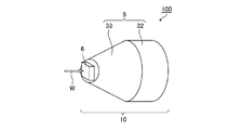
- the magnetic field applying unit 9 may include a permanent magnet 32 and a magnetic flux concentration member 33 that concentrates a magnetic flux generated by the permanent magnet 32 on the cavity resonance unit 2.
- the magnetic flux concentration member 33 is formed of a substantially frustoconical yoke, that is, a magnetic lens.
- FIG. 14 is an application of the electromagnetic wave receiving unit 10 in which the electromagnetic wave input unit 11 is included in the container 6, and each member in the container 6 is not shown, and the power supply 12 is also not shown. Omitted.
- the number of the resonance cavities 22 in the cavity resonance unit 2 may be two or more, and is not limited to six. By increasing the number of the resonance cavities 22, the amplifying effect of the cavity resonance unit 2 can be enhanced, and the reception sensitivity can be further improved. Therefore, the number of the resonance cavities 22 may be set as needed.
- each resonance cavity 22 is not limited to a substantially circular shape.
- Each resonant cavity 22 may be substantially elliptical or substantially polygonal.
- the electromagnetic wave receiver 100 includes the electromagnetic wave receiving unit 10 that receives the input electromagnetic wave W and the behavior of the current flowing through the electromagnetic wave receiving unit 10 (that is, the received current) or the applied voltage. And a signal generator 51 that generates a DC electric signal or an electric signal having a lower frequency than the input electromagnetic wave W.
- the electromagnetic wave receiver 10 receives the electromagnetic wave W.
- an electromagnetic wave W having an arbitrary frequency f can be received with high sensitivity.
- an electromagnetic wave W having a frequency f of 10 THz or more which cannot be received by a conventional electromagnetic wave receiver using the amplifying action of the FET, with high sensitivity.
- the current supply unit has one of the anode and the cathode electrically connected to the tip of the N electrodes 25 included in the resonance cavity 22, and the other of the anode and the cathode connected to the power supply 12.
- N diodes 3 electrically connected in common.
- a current supply unit can be realized by using a PN junction diode, a Schottky barrier diode, or a PIN diode.
- the diode 3 and the conductor plate 1 can be formed using IC manufacturing technology. Further, the manufacture of the electromagnetic wave receiving unit 10 can be facilitated.
- the electromagnetic wave receiver 100 includes a power supply 12 for applying a bias voltage to the diode 3. As a result, an amplification current can be supplied to the cavity resonator 2.
- the size of the N resonance cavities 22 in the cavity resonance section 2 is set to a size corresponding to the frequency f of 10 THz or more. Thereby, an amplifying operation at a frequency f of 10 THz or more can be realized. As a result, the electromagnetic wave W having a frequency f of 10 THz or more can be received with high sensitivity.
- the electromagnetic wave input unit 11 is constituted by the protrusion 42 or the protrusion 43 provided on the cavity resonance unit 2.
- the projection 42 or the projection 43 functions as an input antenna for the electromagnetic wave W, so that the electromagnetic wave input unit 11 can be realized.
- the electromagnetic wave input section 11 is constituted by the widened section 45 of the groove 44 adjacent to the cavity resonance section 2.
- the widening section 45 functions as an input antenna for the electromagnetic wave W, so that the electromagnetic wave input section 11 can be realized.
- the magnetic field applying unit 9 includes the magnetic flux concentration member 33.
- a magnetic field B having sufficient strength to cause an amplification effect can be applied to the cavity resonance section 2 using an inexpensive magnet having a weak magnetic force per unit area.
- FIG. 15A is an explanatory diagram showing a state where a main part of the electromagnetic wave receiver according to Embodiment 2 is viewed from a cross section.
- FIG. 15B is an explanatory diagram showing a state where a part including the cavity resonance part in the electromagnetic wave receiver according to Embodiment 2 is viewed from the front.
- An electromagnetic wave receiver 100a according to Embodiment 2 will be described with reference to FIG. In FIG. 15, the same members and the like as the members and the like shown in FIG.
- a cavity resonating portion 2 having N resonant cavities 22 arranged in an annular shape is provided on a conductive plate 1, and a space in which the tip of an electrode 25 of each resonant cavity 22 faces is provided.
- the filament 14 is inserted through the center, that is, the center of the through hole 21.
- One terminal of the power supply 12 is electrically connected to one end of the filament 14, and the other terminal of the power supply 12 is electrically connected to the conductor plate 1.
- a power supply 15 for heating the filament 14 is provided outside the container 16. Both terminals of the power supply 15 are electrically connected to both terminals of the filament 14.
- the container 16 is a sealed vacuum container, and the filament 14 facing the tip of the electrode 25 of the resonance cavity 22 of the conductor plate 1 is accommodated in a vacuum state in the container 16.
- a so-called “diode vacuum tube” is constituted by the tip of the electrode 25 in the vacuum and the filament 14 heated by the power supply 15.
- This diode vacuum tube structure performs a function equivalent to the function performed by the diode 3 in the electromagnetic wave receiver 100 of the first embodiment. That is, the bipolar vacuum tube structure is a current supply unit that functions to supply an amplification current to the cavity resonance unit 2.
- the conductor plate 1, the cavity resonator 2 having a plurality of (N) resonance cavities 22, the magnetic field applying unit 9, the filament 14, and the container 16 constitute a main part of the electromagnetic wave receiving unit 10a.
- the electromagnetic wave receiver 10a, the electromagnetic wave input unit 11, the power supply 12, the reception determination unit 13, and the power supply 15 constitute a main part of the electromagnetic wave receiver 100a.
- the operation of the electromagnetic wave receiver 100a will be described focusing on the operation of the bipolar vacuum tube structure.
- the reference numerals of the cavity resonance units 2 are omitted. Further, the reference numerals of the respective parts in the cavity resonance section 2 are also omitted from the drawing.
- the magnetic field B (a magnetic field that generates a magnetic flux from the back side toward the surface direction on the paper) is applied to the cavity resonance unit 2, first and clockwise direction along the wall surface portions 24 of the respective first resonant cavity 22 a in a half cycle current I2 BA (see FIG. 16A), the wall portions of the respective second resonant cavity 22 B in the second half cycle 24 And a clockwise current I2 AB (see FIG. 16B) along the line flows alternately.
- amplification current flowing via thermoelectrons e to be described later is added to the resonance currents (I2 BA and I2 AB ) along these wall portions 24, the magnetic energy accumulated in the individual resonance cavities 22 increases. And an amplification effect occurs.
- thermoelectrons e emitted from the filament 14 will be described. Since the inside of the container 16 is in a vacuum state and the filament 14 is heated by the power supply 15, the filament 14 is in a state where it easily emits thermoelectrons e. Therefore, the potential of the first electrode 25 A in the resonance operation at the higher state than the potential of the second electrode 25 B, thermal electrons e are attracted emitted toward the respective first electrodes 25 A absorption while the thermal electrons e are not attracted to the respective second electrodes 25 B, it is hardly absorbed (see FIG. 16A).
- one potential of the second electrode 25 B is in a high state than the potential of the first electrode 25 A, the thermal electrons e is absorbed drawn emitted toward the respective second electrodes 25 B, thermal electrons e are not attracted to the respective first electrodes 25 a, it is hardly absorbed (see FIG. 16B).
- thermoelectrons e perform the same function as the current I3 shown in FIG. 2, that is, the current I3 flowing through each diode 3.
- the amplification current flowing through the electrode 25 to be added with the amplification current can be increased, and the remaining electrodes can be increased. 25 (ie, the low-potential-side electrode 25 at each time) can be suppressed from amplifying current.
- the conduction current can be distributed according to the potential of each electrode 25, and the amplification current can be appropriately supplied to the resonance cavity 22 and the cavity resonance unit 2.
- the internal configuration of the power supply 12 in the electromagnetic wave receiver 100a is the same as that described in Embodiment 1 with reference to FIG.
- the diode vacuum tube structure has the same non-linear voltage-current characteristics as the diode 3. Therefore, the power supply 12 may execute the same constant current control as that described in the first embodiment.
- the electromagnetic wave receiver 100a various modifications similar to the so-called “magnetron” can be used. That is, the magnetron is a device that uses a bipolar vacuum tube structure for generating electromagnetic waves, whereas the electromagnetic wave receiver 100a is a device that uses a bipolar vacuum tube structure for receiving electromagnetic waves W. For this reason, various modifications similar to the magnetron can be adopted.
- a general magnetron generates an electromagnetic wave having a frequency within a frequency range of 3 to 30 GHz, that is, a so-called “microwave”, using a high-voltage power supply that supplies a high voltage of several thousand volts (for example, 3000 volts). Things.
- the electromagnetic wave receiver 100a receives an electromagnetic wave W having a frequency f of, for example, 10 THz or more, using the low-voltage power supply 12 having an output voltage of less than 10 volts.
- the power supply 12 has a different specification from the power supply in a general magnetron, and has a different purpose of use.
- a general magnetron emits high-power electromagnetic waves, and a filament is inserted through a substantially cylindrical anode that also serves as a vacuum vessel, and magnets are provided at both ends of the substantially cylindrical anode. It has a structure that is On the other hand, the electromagnetic wave receiver 100a is provided for receiving a weak electromagnetic wave. The local magnetic field B is applied using the permanent magnet 31. Therefore, the size of the electromagnetic wave receiver 100a can be reduced as compared with a general magnetron so as to correspond to the corresponding power and frequency.
- the electromagnetic wave receiver 100a uses a substantially plate-shaped anode (that is, the conductor plate 1). Thereby, the electromagnetic wave receiver 100a can be made thinner than a general magnetron. As a result, the size of the electromagnetic wave receiver 100a can be further reduced as compared with a general magnetron.
- the electromagnetic wave receiver 100a can employ various modifications similar to those described in the first embodiment.
- the electromagnetic wave receiver 100a includes the electromagnetic wave receiving unit 10 that receives the input electromagnetic wave W and the behavior of the current flowing through the electromagnetic wave receiving unit 10 (that is, the received current) or the applied voltage. And a signal generation unit 51 that generates a DC electric signal or an electric signal having a lower frequency than the input electromagnetic wave W.
- the electromagnetic wave receiver 100a receives the electromagnetic wave W.
- an electromagnetic wave W having an arbitrary frequency f can be received with high sensitivity.
- an electromagnetic wave W having a frequency f of 10 THz or more which cannot be received by a conventional electromagnetic wave receiver using the amplifying action of the FET, with high sensitivity.
- the structure in which the magnetic field applying unit 9 is disposed on one side of the substantially plate-shaped anode allows the electromagnetic wave receiver 100a to be smaller than a general magnetron.
- the current supply unit includes N electrodes 25 included in the resonance cavity 22 of the cavity resonance unit 2 and the filament 14 inserted into the center of the cavity resonance unit 2 (that is, the center of the through hole 21). It has a two-pole vacuum tube structure including a filament 14 electrically connected to the power supply 12 and a vacuum container (container 16) containing the cavity resonator 2 and the filament 14. Since the two-pole vacuum tube structure performs the same function as the N diodes 3, the amplification current can be appropriately supplied to the cavity resonator 2.
- FIG. 17A is an explanatory diagram showing a state where a main part of the electromagnetic wave receiver according to Embodiment 3 is viewed from a cross section.
- FIG. 17B is an explanatory diagram showing a state where a portion including a plurality of cavity resonance portions in the electromagnetic wave receiver according to Embodiment 3 is viewed from the front.
- FIG. 18A is an explanatory diagram showing a state in which a portion including individual cavity resonance portions in the electromagnetic wave receiver according to Embodiment 3 is viewed from a cross section.
- FIG. 18B is an explanatory diagram showing a state where a portion including the individual cavity resonance portions in the electromagnetic wave receiver according to Embodiment 3 is viewed from the front.
- Embodiment 3 An electromagnetic wave receiver 100b according to Embodiment 3 will be described with reference to FIGS. 17 and 18, the same reference numerals are given to the same members and the like as those shown in FIG.
- a plurality (M) of substantially circular through holes 71 are formed in the conductor plate 1.
- a conductor layer 73 is laminated on a portion of the conductor plate 1 including the individual through-holes 71 via a resistance layer 72.
- Each resistance layer 72 is provided with a substantially circular through hole 74, and each conductor layer 73 is provided with a cavity resonator 2.
- the resonance cavities 22 in the individual cavity resonance sections 2 are connected to the conductor plate 1 via the corresponding resistance layers 72 among the M resistance layers 72.
- the electromagnetic wave receiver 100b has M cavity resonators 2.
- Each cavity resonator 2 has the same structure as that described in the first embodiment. For this reason, a detailed description of each cavity resonator 2 will be omitted.
- FIGS. 17 and 18, reference numerals of respective portions in the individual cavity resonance sections 2 are omitted.
- Each cavity resonance part 2 has N electrodes 25, and the anodes of N diodes 3 are electrically connected to the tips of the N electrodes 25, respectively.
- the cathodes of the N diodes 3 are electrically connected to the substrate 5 in common.
- One terminal of the power supply 12 is electrically connected to the conductor plate 1, and the other terminal of the power supply 12 is electrically connected to the substrate 5.
- the electromagnetic wave receiver 100b is electrically configured by connecting M amplification structures similar to those described in the first embodiment in parallel.
- the area of the portion for receiving the electromagnetic wave W can be increased, so that the reception sensitivity can be further improved.
- the electromagnetic wave W is light
- the cavity resonating portion 2 enlarging the light receiving area
- the respective light receiving amounts are summed up. The total amount of received light can be increased, and an optical sensor with higher sensitivity can be realized.
- the electromagnetic wave receiver 100 b has the resistance layer 72.
- the resistance layer 72 has a function of preventing the amplification current from being concentrated on a part of the M cavity resonators 2.
- the resistance layer 72 has a function of distributing the amplification current to the M cavity resonance sections 2 by limiting the supply of the amplification current to the individual cavity resonance sections 2.
- a part that performs the function in the electromagnetic wave receiver 100b is referred to as a “current limiting part”.
- the electromagnetic wave input unit 11 is constituted by the protrusions 42 provided on the individual cavity resonance units 2. For this reason, the electromagnetic wave input unit 11 is included in the electromagnetic wave receiving unit 10b.
- the main part of the electromagnetic wave receiver 100b is thus configured.
- the current limiting section only has to perform the above function, and is not limited to the resistance layer 72 shown in FIG. 17 and FIG.
- the current limiting portion may be configured by the resistance layer 75 laminated on the substrate 5, that is, the resistance layer 75 provided between the diode 3 and the substrate 5.
- the conductor layer 73 is also unnecessary. That is, the cavity layer 2 may be provided in the conductor plate 1 as shown in FIG. 1 even in the configuration as shown in FIGS. 17 and 18 by removing the resistance layer 72 and the conductor layer 73.
- the individual diodes 3 may be constituted by PIN diodes, so that the resistance component of the PIN diodes may function as a current limiting unit.
- an intrinsic semiconductor layer hereinafter, referred to as an “I layer” in the PIN diode serves as a resistance component and functions as a current limiting unit.
- a conductor layer 84 made of metal foil is formed on a PIN diode composed of a P layer 83, and the cavity resonance section 2 is provided in the conductor layer 84 (corresponding to the conductor plate 1). It may be.
- the resistance component of the diode 3, that is, the I layer 82 of the PIN diode may function as a current limiting unit.
- the metal foil serving as the conductor layer 84 serves as a wiring or an electrode
- the substrate 5 corresponds to a lead frame for mounting a semiconductor chip.
- the cavity 85, the cavity resonator 2, and the projection 42 serving as the electromagnetic wave input unit 11 shown in FIG. 21 are formed by, for example, etching or FIB (Focused Ion Beam) processing.
- an insulating layer 94 and a metal foil are formed on a PIN diode composed of an N layer 91, an I layer 92, and a P layer 93 provided on the entire surface of the I layer. May be provided, and the cavity layer 2 may be provided in the conductor layer 95 (corresponding to the conductor plate 1). Note that, in this configuration, while the tip of the electrode 25 of the resonance cavity 22 is connected to the P layer 93, the portion other than the tip is insulated by the insulating layer 94. Also in this case, the I layer 92 functions as a current control unit.
- the hollow part 96, the hollow resonance part 2, and the protrusion 42 which becomes the electromagnetic wave input part 11 shown in FIG. 22 are formed by, for example, etching or FIB processing.
- the conductor layer 84 forming the cavity resonance section 2 in the electromagnetic wave receiving section 10b may be divided into M layers, or may be one without being divided. The same applies to the conductor layer 95 in the example shown in FIG.
- the number of the cavity resonators 2 may be two or more, and is not limited to five.
- the electromagnetic wave receiver 100b may have two cavity resonators 2, may have three cavity resonators 2, and may have six or more cavity resonators. 2 may be provided.
- the electromagnetic wave input unit 11 in the electromagnetic wave receiver 100b is not limited to the protrusion 42 provided on each cavity resonance unit 2.
- the projections 43 may be provided on each of the cavity resonance sections 2, and the electromagnetic wave input section 11 may be configured by these projections 43.
- grooves 44 may be provided adjacent to the individual cavity resonating portions 2, and the electromagnetic wave input section 11 may be configured by the widened portions 45 of these grooves 44.
- the cavity resonance units 2 (specifically, the protrusions 43 serving as the electromagnetic wave input units 11) are regularly arranged. It is possible to arbitrarily set a direction having high sensitivity to the input electromagnetic wave W, that is, directivity.
- two cavity resonators 2 are provided on the conductor plate 1, and each of the two cavity resonators 2 is provided with a projection 43.
- These two projections 43 are arranged on a straight line SL, and the interval D1 between the two projections 43 is set to a value n times the wavelength ⁇ .
- directivity with high sensitivity to the electromagnetic wave W input from a total of four directions including two directions along the straight line SL and two directions orthogonal to the straight line SL can be realized.
- two cavity resonators 2 are provided on the conductor plate 1, and the projections 43 are provided on each of the two cavity resonators 2.
- These two projections 43 are arranged on a straight line SL, and the interval D2 between the two projections 43 is set to a value (n ⁇ /) times the wavelength ⁇ (n is 1). Any integer greater than or equal to). In this case, directivity with high sensitivity to electromagnetic waves W input from two directions along the straight line SL can be realized.
- three cavity resonators 2 are provided on the conductor plate 1, and the projections 43 are provided on each of the three cavity resonators 2.
- These three projections 43 are arranged on a straight line SL, and the distance D3 between each two adjacent projections 43 of the three projections 43 is set to a value of n / 2 times the wavelength ⁇ . Is set. In this case, it is possible to obtain directivity with higher sensitivity to electromagnetic waves W input from two directions along the straight line SL.
- the electromagnetic wave receiver 100b having a predetermined directivity pattern can be realized.
- the plurality of (M) cavity resonators 2 may include the cavity resonators 2 having different resonance frequencies f.
- the resonance frequency f of one cavity resonator 2 and the resonance frequency f of the other cavity resonator 2 are different from each other. Is also good. That is, the dimensions of the individual resonance cavities 22 (more specifically, the creepage length L1) in the one cavity resonance part 2 and the dimensions of the individual resonance cavities 22 in the other cavity resonance part 2 (more specifically, the creepage length L1) ) May be different from each other. Thereby, the electromagnetic waves W having different frequencies f can be simultaneously received.
- each resonance cavity 22 in the first cavity resonator 2 is a value corresponding to the wavelength ⁇ of red visible light.
- the dimensions of the individual resonant cavities 22 in the second cavity resonating section 2 are set to values corresponding to the wavelength ⁇ of green visible light, and the third cavity resonating section 2 May be set to a value corresponding to the wavelength ⁇ of blue visible light.
- the electromagnetic wave receiver 100b can be used for a so-called “RGB color sensor”.
- the electromagnetic wave receiver 100b can employ various modifications similar to those described in the first embodiment.
- the electromagnetic wave receiving unit 10b has a plurality (M) of the cavity resonance units 2.
- M the number of the cavity resonators 2
- the area of the part that receives the electromagnetic wave W can be increased, and thus the reception sensitivity can be adjusted as needed.
- the plurality of (M) cavity resonators 2 include cavity resonators 2 having different resonance frequencies f. Thereby, the electromagnetic waves W having different frequencies f can be simultaneously received. As a result, for example, the electromagnetic wave receiver 100b can be used for an RGB color sensor.
- a plurality (M) of cavity resonators 2 are regularly arranged. Accordingly, it is possible to realize the electromagnetic wave receiver 100b having a directivity pattern with increased sensitivity to the electromagnetic wave W from a predetermined direction.
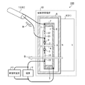
- FIG. 26 is an explanatory diagram illustrating a main part of the radar device according to the fourth embodiment. With reference to FIG. 26, a radar device 200 according to the fourth embodiment will be described.
- a radar device 200 including an electromagnetic wave receiver 100 and an electromagnetic wave transmitter 110 is provided in a vehicle 500.
- the electromagnetic wave transmitter 110 generates an electromagnetic wave W having a frequency f between a millimeter wave and an infrared ray, and transmits the generated electromagnetic wave W to the outside of the vehicle 500.
- the electromagnetic wave receiver 100 receives the reflected electromagnetic wave W.
- the electromagnetic wave receiver 100 has the same structure as that described in the first embodiment. Therefore, description of the electromagnetic wave receiver 100 is omitted. However, the dimensions of the individual resonance cavities 22 (more specifically, the creepage length L1) are set to values corresponding to the frequency f between the millimeter wave and the infrared light. In FIG. 26, each part in the electromagnetic wave receiver 100 is not shown.
- the electromagnetic wave transmitter 110 may have the same structure as a general magnetron, or may have the same structure as the electromagnetic wave receiver 100.
- the electromagnetic wave transmitter 110 can transmit an electromagnetic wave W having a frequency f between millimeter waves and infrared rays, that is, a frequency f corresponding to the size (size) of each resonance cavity 22 in the electromagnetic wave receiver 100. Any structure may be used.
- the radar signal processing unit 120 outputs a predetermined electric signal to the electromagnetic wave transmitter 110 so that the electromagnetic wave transmitter 110 transmits the electromagnetic wave W. Further, when the electromagnetic wave W is received by the electromagnetic wave receiver 100, the radar signal processing unit 120 executes a so-called “radar signal processing” using an electric signal corresponding to the received electromagnetic wave W. That is, the radar signal processing unit 120 executes the radar signal processing by using the electric signal generated by the signal generation unit 51 when the reception determination unit 13 determines that the electromagnetic wave W is received.
- the control unit 130 controls the operation of the radar signal processing unit 120. Further, when the obstacle O is detected by the radar signal processing, the control unit 130 instructs the vehicle control device 300 to execute control for avoiding a collision between the vehicle 500 and the obstacle O. The vehicle control device 300 executes control for avoiding the collision by operating a brake or steering of the vehicle 500 in accordance with an instruction from the control unit 130.
- the vehicle control device 300 is configured by, for example, an ECU (Electronic Control Unit).
- the warning output device 400 includes, for example, a display or a speaker.
- the warning output device 400 is configured by a display, the warning is based on an image display.
- the warning output device 400 is configured by a speaker, the warning is based on a sound output or a warning sound.
- the electromagnetic wave receiver 100, the electromagnetic wave transmitter 110, the radar signal processing unit 120, and the control unit 130 constitute a main part of the radar device 200.
- the radar device 200 has a processor 140 and a memory 150.
- the memory 150 stores a program for realizing the functions of the radar signal processing unit 120 and the control unit 130.
- the functions of the radar signal processing unit 120 and the control unit 130 are realized by the processor 140 reading and executing the program stored in the memory 150.
- the radar device 200 has a processing circuit 160.
- the functions of the radar signal processing unit 120 and the control unit 130 are realized by the dedicated processing circuit 160.
- the radar device 200 has a processor 140, a memory 150, and a processing circuit 160 (not shown).
- some of the functions of the radar signal processing unit 120 and the control unit 130 are realized by the processor 140 and the memory 150, and the remaining functions are realized by the dedicated processing circuit 160.
- the processor 140 uses, for example, at least one of a CPU (Central Processing Unit), a GPU (Graphics Processing Unit), a microprocessor, a microcontroller, or a DSP (Digital Signal Processor).
- a CPU Central Processing Unit
- GPU Graphics Processing Unit
- microprocessor a microcontroller
- DSP Digital Signal Processor
- the memory 150 uses, for example, at least one of a semiconductor memory and a magnetic disk. More specifically, the memory 150 includes a RAM (Random Access Memory), a ROM (Read Only Memory), a flash memory, an EPROM (Erasable Programmable Read Memory Only), and an EEPROM (Electrical Memory). At least one of State @ Drive or HDD (Hard @ Disk @ Drive) is used.
- RAM Random Access Memory
- ROM Read Only Memory
- flash memory an EPROM (Erasable Programmable Read Memory Only)
- EEPROM Electrical Memory
- the processing circuit 160 includes, for example, an ASIC (Application Specific Integrated Circuit), a PLD (Programmable Logic Device), an FPGA (Field-Programmable Gate System Array), and an SoC (Sig-Lig- At least one of them is used.
- ASIC Application Specific Integrated Circuit
- PLD Programmable Logic Device
- FPGA Field-Programmable Gate System Array
- SoC So-Lig- At least one of them is used.
- millimeter-wave radar or infrared laser radar has been used as a vehicle-mounted radar.
- the obstacle O is a low-density resin molded product (for example, styrene foam) or a cloth using fine fibers
- the millimeter wave passes through the obstacle O, and thus such an obstacle is detected using a millimeter wave radar.
- the object O could not be detected.
- particles such as raindrops or fog exist between the vehicle 500 and the obstacle O
- the laser light is blocked by these particles, so that there is a problem that the obstacle O cannot be detected using the infrared laser radar.
- the radar apparatus 200 can detect the obstacle O even in these cases.
- the electromagnetic wave receiver 100 can be used for receiving an electromagnetic wave W having an arbitrary frequency f.
- the electromagnetic wave W transmitted and received by the radar device 200 is not limited to the electromagnetic wave W having the frequency f between the millimeter wave and the infrared ray, but may be a millimeter wave or an infrared ray.
- a millimeter wave radar or an infrared laser radar can be realized.
- the electromagnetic wave transmitter 110 may be similar to a transmitter in a conventional millimeter wave radar or infrared laser radar.
- the radar device 200 may have the electromagnetic wave receiver 100a or the electromagnetic wave receiver 100b instead of the electromagnetic wave receiver 100.
- the application of the radar device 200 is not limited to the on-vehicle radar.
- the radar device 200 may be used for radar for any purpose.
- the radar device 200 includes the electromagnetic wave receiver 100, the electromagnetic wave receiver 100a, or the electromagnetic wave receiver 100b.
- the electromagnetic wave receiver 100, the electromagnetic wave receiver 100a, or the electromagnetic wave receiver 100b it is possible to realize a radar device 200 capable of receiving an electromagnetic wave W having an arbitrary frequency f.
- the radar device 200 capable of receiving the electromagnetic wave W having the frequency f between the millimeter wave and the infrared light.
- the electromagnetic wave receiver of the present invention can be used, for example, for receiving electromagnetic waves having a frequency in the terahertz range.
Landscapes
- Engineering & Computer Science (AREA)
- Physics & Mathematics (AREA)
- General Physics & Mathematics (AREA)
- Computer Networks & Wireless Communication (AREA)
- Radar, Positioning & Navigation (AREA)
- Remote Sensing (AREA)
- Spectroscopy & Molecular Physics (AREA)
- Photometry And Measurement Of Optical Pulse Characteristics (AREA)
- Waveguide Aerials (AREA)
- Radar Systems Or Details Thereof (AREA)
- Optical Radar Systems And Details Thereof (AREA)
- Input Circuits Of Receivers And Coupling Of Receivers And Audio Equipment (AREA)
Abstract
電磁波受信機(100)は、入力された電磁波(W)を受信する電磁波受信部(10)と、電磁波受信部(10)に流通する電流又は印加する電圧の挙動を用いて、直流の電気信号又は入力された電磁波(W)よりも低周波の電気信号を生成する信号生成部(51)と、を備える電磁波受信機(100)であって、電磁波受信部(10)は、電磁波(W)を入力する電磁波入力部(11)と、導体板(1)に設けた空洞共振部(2)と、空洞共振部(2)に増幅用の電流を供給する電流供給部(3)と、導体板(1)の片面側に配置され、空洞共振部(2)に磁界(B)を印加する磁界印加部(9)と、を有する。
Description
本発明は、電磁波受信機及びレーダ装置に関する。
従来、30~300ギガヘルツ(GHz)の周波数領域内の周波数を有する電磁波、いわゆる「ミリ波」用の受信機が開発されている。これに対して、特許文献1には、0.1~10テラヘルツ(THz)の周波数領域内の周波数を有する電磁波、いわゆる「テラヘルツ波」用の受信機が開示されている。
特許文献1記載の受信機は、アンテナに電磁波が入力されたとき、FET(Field Effect Transistor)を用いて、当該入力された電磁波に対応する電気信号を増幅するものである。通常、FETが有する周波数特性により、FETを用いて10THz以上の周波数を有する電気信号を増幅することは困難である。このため、特許文献1記載の受信機は、10THz以上の周波数を有する電磁波に対する受信感度が低いという問題があった。すなわち、特許文献1記載の受信機は、10THz以上の周波数を有する電磁波の受信に用いることができないという問題があった。
本発明は、上記のような課題を解決するためになされたものであり、広い周波数範囲に亘り高い受信感度を有する電磁波受信機を提供することを目的とする。また、この電磁波受信機を用いたレーダ装置を提供することを目的とする。
本発明の電磁波受信機は、入力された電磁波を受信する電磁波受信部と、電磁波受信部に流通する電流又は印加する電圧の挙動を用いて、直流の電気信号又は入力された電磁波よりも低周波の電気信号を生成する信号生成部と、を備える電磁波受信機であって、電磁波受信部は、電磁波を入力する電磁波入力部と、導体板又は導体層に設けた複数個の共振空洞を有する空洞共振部と、空洞共振部に増幅用の電流を供給する電流供給部と、導体板又は導体層の片面側に配置され、空洞共振部に磁界を印加する磁界印加部と、を有するものである。また、本発明のレーダ装置は、この電磁波受信機を備えるものである。
本発明によれば、上記のように構成したので、広い周波数範囲に亘り高い受信感度を有する電磁波受信機を得ることができる。また、この電磁波受信機を用いたレーダ装置を得ることができる。
以下、この発明をより詳細に説明するために、この発明を実施するための形態について、添付の図面に従って説明する。
実施の形態1.
図1Aは、実施の形態1に係る電磁波受信機の要部を断面から見た状態を示す説明図である。図1Bは、実施の形態1に係る電磁波受信機における空洞共振部を含む部位を正面から見た状態を示す説明図である。図1を参照して、実施の形態1の電磁波受信機100について説明する。
図1Aは、実施の形態1に係る電磁波受信機の要部を断面から見た状態を示す説明図である。図1Bは、実施の形態1に係る電磁波受信機における空洞共振部を含む部位を正面から見た状態を示す説明図である。図1を参照して、実施の形態1の電磁波受信機100について説明する。
図1に示す如く、導体板1に空洞共振部2が設けられている。より具体的には、1個の略円形状の貫通孔21が導体板1に穿たれており、かつ、貫通孔21の周囲に円環状に配列された複数個(N個)の略円形状の貫通孔22(共振空洞22)が導体板1に穿たれている。ここで、Nは2以上の任意の偶数であり、図1に示す例においてはN=6である。個々の貫通孔22は、貫通孔21に対する開口部23を有しており、貫通孔21と連通している。個々の貫通孔22の壁面部24の沿面長L1は、電磁波受信機100により受信される電磁波Wの波長λに対する1/2倍の値に設定されている。個々の貫通孔22により、共振空洞22が構成されている。以下貫通孔22を共振空洞22と記載することもある。
互いに隣接する各2個の共振空洞22間の導体により、すなわち導体板1のうちの互いに隣接する各2個の共振空洞22間の部位により、個々の電極25が形成されている。したがって、電極25の個数は共振空洞22の個数と同一であり、空洞共振部2はN個の共振空洞22及びN個の電極25を有するものである。
個々の共振空洞22は、開口部23を介して互いに対向配置された2個の電極25の先端部がキャパシタの機能を果たすとともに、いわゆる「表皮効果」により略環状の壁面部24がコイルの機能を果たすことにより、LC共振回路の機能を果たすものである。ここで、沿面長L1が波長λに対する1/2倍の値に設定されていることにより、このLC共振回路における共振周波数fはf=電磁波Wの速度/λ=電磁波Wの速度/2L1となるものである。すなわち、このLC共振回路における共振周波数fに応じて、電磁波受信機100により受信される電磁波Wの周波数fが設定されるものである。
N個の電極25の先端部にN個のダイオード3のアノードが電気的にそれぞれ接続されている。N個のダイオード3のカソードは、導体棒4を介して基板5と電気的に共通接続されている。個々のダイオード3は、例えば、PN接合ダイオード、ショットキーバリアダイオード又はPINダイオード等により構成されている。基板5は導電性を有するものであり、容器6内にて導体板1と対向配置されている。基板5と導体板1間に設けられた絶縁部材7により、基板5と導体板1間に間隙8が形成されている。
ここで、N個の共振空洞22は、便宜的なN/2個の共振空洞(以下「第1共振空洞」ということがある。)22Aと残余のN/2個の共振空洞(以下「第2共振空洞」ということがある。)22Bとが交互に配置されたものである。N個の電極25は、便宜的なN/2個の電極(以下「第1電極」ということがある。)25Aと残余のN/2個の電極(以下「第2電極」ということがある。)25Bとが交互に配置されたものである。N個のダイオード3は、便宜的なN/2個のダイオード(以下「第1ダイオード」ということがある。)3Aと残余のN/2個のダイオード(以下「第2ダイオード」ということがある。)3Bとが交互に配置されたものである。
なお、ダイオードを使用する電磁波受信機100においては、容器6内を真空状態にすることは不要である。このため、容器6は密封容器でなくとも良い。
容器6外にて、導体板1の片面側(すなわち基板5の片面側)に磁界印加部9が設けられている。図1に示す例において、磁界印加部9は永久磁石31により構成されている。磁界印加部9は、導体板1の板面(すなわち基板5の板面)に対する直交方向の磁束を発する磁界Bを空洞共振部2に印加するものである。
導体板1、空洞共振部2、ダイオード3、導体棒4、基板5、容器6、絶縁部材7及び磁界印加部9により、電磁波受信部10の要部が構成されている。
容器6外に電磁波入力部11が設けられている。電磁波入力部11は、電磁波Wを入力するものである。図1に示す例において、電磁波入力部11は電磁波W用の伝送線路41により構成されている。伝送線路41は、例えば、同軸ケーブル又は導波管により構成されている。
なお、電磁波入力部11と空洞共振部2間の接続線路には、電磁波Wの波長λに応じた部材を用いる必要がある。例えば、電磁波Wが可視光である場合、当該接続線路には可視光を透過する材料(透明なガラス、透明なセラミックス又は透明な樹脂など)を用いる必要があり、電磁波Wが赤外線である場合、当該接続線路には赤外線を透過する材料を用いる必要がある。
容器6外に電源12が設けられている。電源12における一方の端子は導体板1と電気的に接続されており、電源12における他方の端子は基板5と電気的に接続されている。これにより、N個のダイオード3のカソードは導体棒4及び基板5を介して電源12と電気的に共通接続されている。電源12は、空洞共振部2による増幅用の電流(以下「増幅用電流」という。)を供給するものであり、かつ、ダイオード3にバイアス電圧を印加するものである。
すなわち、電磁波受信部10は電磁波入力部11に入力された電磁波Wを受信するものである。より具体的には、電磁波受信部10は、増幅用電流を用いて電磁波Wに対応する電流を増幅するものである。この増幅作用は空洞共振部2によるものであり、N個のダイオード3は増幅用電流を空洞共振部2に供給する機能を果たすものである。空洞共振部2による増幅作用の詳細については、図2及び図3を参照して後述する。以下、電磁波受信機100において、増幅用電流を空洞共振部2に供給する機能を果たす部位を「電流供給部」という。
容器6外に受信判定部13が設けられている。受信判定部13は、電源12により供給され電磁波受信部10に流通する電流又は印加する電圧の挙動に基づいて、電磁波受信部10による電磁波Wの受信の有無を判定するものである。
電磁波受信部10、電磁波入力部11、電源12及び受信判定部13により、電磁波受信機100の要部が構成されている。
空洞共振部2は、個々の共振空洞22の寸法(大きさ)に応じて、より具体的には沿面長L1の値に応じて、任意の周波数fの電磁波Wを増幅することができる。このため、電磁波受信機100は、個々の共振空洞22の寸法を調整して、より具体的には沿面長L1の値を調整して、任意の周波数fを有する電磁波Wの受信に用いることができる。
例えば、沿面長L1が300マイクロメートル(μm)に設定されている場合、1THzの周波数fの電磁波を増幅することができる。このため、1THzの周波数fを有する電磁波Wを受信することができる。また、沿面長L1が0.3μmに設定されている場合、1000THzの周波数fの電磁波を増幅する。このため、1000THzの周波数fを有する電磁波Wを受信することができる。このように、沿面長L1を0.3~300μmの範囲内の値に設定することにより、1~1000THzの周波数領域(以下「テラヘルツ領域」という。)内の周波数fを有する電磁波Wを受信することができる。
テラヘルツ領域内の周波数fを有する電磁波Wは、種々の技術分野に対する応用が進められている。例えば、人体用の透視装置、車載用のレーダ装置、生体分子の同定、電子材料の物性評価、非破壊計測及び医療機器などの技術分野に対する応用が進められている。したがって、電磁波受信機100は、これらの技術分野に応用することができる。
ちなみに、沿面長L1が300μmよりも大きい値に設定されている場合、1THzよりも低い周波数fの電磁波を増幅する。このため、1THzよりも低い周波数fを有する電磁波Wを受信することができる。このように、沿面長L1を300μmよりも大きい値に設定することにより、テラヘルツ領域に比して低い周波数領域内の周波数fを有する電磁波Wを受信することもできる。
なお、沿面長L1が2.5~12.5μm程度の値に設定されている場合、対応する電磁波Wは遠赤外線となる。沿面長L1が0.2~0.4μm程度の値に設定されている場合、対応する電磁波Wは可視光となる。沿面長L1が約300ナノメートル(nm)の値に設定されている場合、対応する電磁波Wは黄色の可視光となる。このように、電磁波受信機100は光の受信に用いることもできる。
これらの具体例において、空洞共振部2のサイズはマイクロメートル単位又はナノメートル単位である。かかる微小な空洞共振部2を有する導体板1は、例えば、いわゆる「3Dプリンタ」を用いて製造される。または、例えば、IC(Integrated Circuit)における導体パターン形成用の微細加工技術(メッキ、蒸着、折出又はエッチングなど)を用いて製造される。または、例えば、いわゆる「メタマテリアル」における導電性材料用の微細加工技術を用いて製造される。
また、空洞共振部2のサイズが微小であるため、導体板1の片面側に設けられた永久磁石31を用いて板面に対する直交方向の磁束を発する磁界Bを印加することができる。なお、図1に示す例においては、磁界印加部9を容器6外に設けているが、効果的に磁界を印加するために、容器6の内側に設けて導体板1に接近させてもよい。
ただし、電磁波Wの周波数fを低くすることが要求される場合、個々の共振空洞22の寸法が大きくなり、空洞共振部2のサイズが上記の具体例に比して大きくなることがある。また、受信感度を更に向上することが要求される場合、共振空洞22の個数が増加して、空洞共振部2のサイズが上記の具体例に比して大きくなることがある。これにより、導体板1の片面側に配置された永久磁石31だけでは板面に対する十分な直交方向の磁束を発する磁界Bを印加することが困難となる可能性がある。この場合、2個の磁石により磁界印加部9が構成され、当該2個の磁石間に容器6が配置されているものであっても良い。
次に、図2及び図3を参照して、電磁波受信機100の動作について、空洞共振部2による増幅作用を中心に説明する。なお、図2において、空洞共振部2の符号、ダイオード3の符号及び導体棒4の符号は図示を省略している。また、空洞共振部2における各部位の符号も図示を省略している。
図2におけるI1は、電源12による供給電流、すなわち増幅用電流の向きを示している。図2におけるI2(I2AB及びI2BA)は、空洞共振部2に流れる電流、より具体的には個々の共振空洞22に流れる電流(以下「共振電流」ということがある。)の向きを示している。図2におけるI3(I3A及びI3B)は、個々のダイオード3に流れる電流(以下「通電電流」ということがある。)の向きを示している。なお、I1は、電磁波受信部10に流通する電流、すなわち空洞共振部2に流れる電流(以下「受信電流」ということがある。)の向きを示すものでもある。以下、図2における紙面時計回り方向を単に「時計回り方向」といい、図2における紙面反時計回り方向を単に「反時計回り方向」という。
電磁波入力部11が電磁波Wを入力することにより、当該入力された電磁波Wに対応する電流が空洞共振部2に供給される。ここで、上記のとおり、個々の共振空洞22はLC共振回路の機能を果たすものである。仮に空洞共振部2に磁界Bが印加されていない場合、個々の共振空洞22の壁面部24に沿うようにして、各共振周期のうちの前半周期(以下「第1半周期」という。)にて第2電極25Bから第1電極25Aに向かう電流I2BAが流れるとともに、各共振周期のうちの後半周期(以下「第2半周期」という。)にて第1電極25Aから第2電極25Bに向かう電流I2ABが流れる状態となる。すなわち、個々の共振空洞22のそれぞれの壁面部24においては、壁面部24に沿う時計回り方向の電流I2と、反時計回り方向の電流I2とが、同じ壁面部24に交互に流れる状態となる。
これに対して、磁界B(紙面においては裏側から表面方向に向かう磁束を発する磁界)が印加されていることにより、空洞共振部2における導体内を移動する電子に反時計回り方向の力Fが加わる。これにより、電子の軌道Tが反時計回り方向に曲げられることにより、電流I2は時計回り方向の電流I2BA,I2ABが多く流れるようになる。この結果、図2Aに示す第1半周期においては個々の第1共振空洞22Aの壁面部24に沿う時計回り方向の電流I2BAが流れるとともに、図2Bに示す第2半周期においては個々の第2共振空洞22Bの壁面部24に沿う時計回り方向の電流I2ABが流れる状態となる。すなわち、図2Aに示す時計回り方向の電流I2BAと図2Bに示す時計回り方向の電流I2ABとが交互に流れる状態であって、反時計回り方向の電流I2は流れない状態となる。
また、電源12が供給する増幅用の電流がダイオード3を介して空洞共振部2に供給される。この増幅用電流も上記のように振る舞う(すなわち、空洞共振部2の導体内を移動する増幅用電流の電子にも磁界Bによって、反時計回り方向の力Fが加わり、増幅用電流は個々の共振空洞22の壁面部24に沿うように偏って流れる)ため、第1と第2のそれぞれの半周期において、増幅用電流が共振電流と同じ壁面部24に同じ方向に流れる。共振電流と同じタイミングで同じ方向に増幅用電流が流れることによって、壁面部24に流れる共振電流に増幅用電流が加算される。
第1半周期においては、共振電流に増幅用電流を加算してなる電流に対応する磁気エネルギーが個々の第1共振空洞22Aに蓄積されて、次いで、共振動作によって当該蓄積された磁気エネルギーが電荷エネルギーに変換される。このときの増幅用電流は第1ダイオード3Aに電流I3Aとなって流れる。続く第2半周期においては、当該変換された電荷エネルギーが共振動作によって個々の第2共振空洞22Bに流出することにより、個々の第2共振空洞22Bに共振電流が流れる。この共振電流に増幅用電流が更に加算されることにより、前回蓄積された磁気エネルギーよりも大きい磁気エネルギーが個々の第2共振空洞22Bに蓄積されて、次いで、共振動作によって当該蓄積された大きな磁気エネルギーが次の電荷エネルギーに変換される。このときの増幅用電流は第2ダイオード3Bに電流I3Bとなって流れる。以後また第1半周期の動作に至り上記が繰り返され、共振電流に増幅用電流が加算される毎に個々の共振空洞22に蓄積される磁気エネルギーが大きくなり、増幅作用が生ずる。
ここで、電極25の先端部の挙動について説明を加える。電流I2BAと電流I2ABが交互に流れて振動しているときには、個々の電極25の電位も振動する。すなわち、第1電極25Aの電位が第2電極25Bの電位に比して高い状態と第2電極25Bの電位が第1電極25Aの電位に比して高い状態とが交互に繰り返される。換言すれば、第2電極25Bの電位が第1電極25Aの電位に比して低い状態と第1電極25Aの電位が第2電極25Bの電位に比して低い状態とが交互に繰り返される。
これに対して、上記のとおり、N個の電極25の先端部にN個のダイオード3のアノードが電気的にそれぞれ接続されている。ダイオード3が有する電圧―電流特性により、第1電極25Aの電位が第2電極25Bの電位に比して高い状態においては、第1ダイオード3Aに電流I3Aが流れる一方、第2ダイオード3Bには電流I3Bがほとんど流れない(図2A参照)。また、第2電極25Bの電位が第1電極25Aの電位に比して高い状態においては、第2ダイオード3Bに電流I3Bが流れる一方、第1ダイオード3Aには電流I3Aがほとんど流れない(図2B参照)。
したがって、N個の電極25のうちの増幅用電流の加算対象となる電極25(すなわち各時刻における高電位側の電極25)に流れる増幅用電流を増長することができ、かつ、残余の電極25(すなわち各時刻における低電位側の電極25)に流れる増幅用電流を抑制することができる。このように、N個の電極25のそれぞれの先端部にN個のダイオード3が設けられていることにより、それぞれの電極25の電位によって通電電流を振り分けることができ、増幅用電流を適切に共振空洞22さらには空洞共振部2に供給することができる。
以上の動作により、電磁波Wを入力すると個々の共振空洞22における共振状態(すなわち個々のLC共振回路における共振状態)が発生して、電磁波Wに対応する電流が増加する。見方を変えれば、電磁波Wが入力されると空洞共振部2へ供給する増幅用電流が流れ易くなる。したがって、印加電圧を低下させても同等の電流を供給することができる。つまり、空洞共振部2に定電流を供給する構成にすれば、空洞共振部2への印加電圧の低下によって電磁波Wの受信を検知することが可能であり、この動作により、電磁波Wを高感度に受信することができる。
図3Aは、電磁波Wに対応する電圧の値(図中I)及び電磁波Wに対応する電流の値(図中II)を示すタイミング図である。
図3Bは、個々の第1電極25Aにおける電位の値(図中III)、個々の第1電極25Aにおける電流の値(図中IV)及び個々の第1ダイオード3Aにおけるバイアス電圧の値(図中V)を示すタイミング図である。なお、個々の第1電極25Aにおける電位の値(図中III)は、個々の第1ダイオード3Aにおける印加電圧の値に対応するものである。個々の第1電極25Aにおける電流の値(図中IV)は、個々の第1ダイオード3Aにおける通電電流の値に対応するものである。
図3Cは、個々の第2電極25Bにおける電位の値(図中VI)、個々の第2電極25Bにおける電流の値(図中VII)及び個々の第2ダイオード3Bにおけるバイアス電圧の値(図中VIII)を示すタイミング図である。なお、個々の第2電極25Bにおける電位の値(図中VI)は、個々の第2ダイオード3Bにおける印加電圧の値に対応するものである。個々の第2電極25Bにおける電流の値(図中VII)は、個々の第2ダイオード3Bにおける通電電流の値に対応するものである。
図3Dは、第1電極25Aから第2電極25Bに流れる電流I2ABの値(図中IX)を示すタイミング図である。図3Eは、第2電極25Bから第1電極25Aに流れる電流I2BAの値(図中X)を示すタイミング図である。図3Fは、第1電極25Aと第2電極25B間の電位差の値(図中XI)を示すタイミング図である。
図3Gは、受信電流の値(図中XII)及び受信電流の平均値(図中XIII)を示すタイミング図である。なお、受信電流の値(図中XII)は、N個のダイオード3における通電電流の合計値に対応するものである。受信電流の平均値(図中XIII)は、N個のダイオード3における通電電流の合計値の平均値に対応するものである。
以下、N個のダイオード3における通電電流の合計値の平均値を「合計平均通電電流」ということがある。また、個々のダイオード3における通電電流の平均値を「個別平均通電電流」ということがある。
ここで、図3B及び図3Cに示す如く、空洞共振部2の増幅作用により個々の電極25における電位の振幅が大きくなるにつれて、個々のダイオード3におけるバイアス電圧が次第に低下している。なお、過大な電磁波Wを入力すれば、バイアス電圧が反転するが、微弱な電磁波Wの受信には、当該領域の動作は必要ない。
なお、図3Gに示す如く、受信電流の振幅が次第に大きくなるにもかかわらず、合計平均通電電流が一定値に保たれているのは、電源12が、ダイオード3に対するバイアス電圧を変化させることにより合計平均通電電流を一定値に保つ制御(以下「定電流制御」という。)を実行しているためである。
次に、図4及び図5を参照して、電磁波受信機100の動作について、電源12による定電流制御を中心に説明する。
図4Aは、ダイオード3が有する電圧―電流特性を示している。通常、ダイオード3は、図4Aに示す如く非線形な電圧―電流特性を有している。これにより、ダイオード3は、印加電圧が所定の順方向電圧VF(例えば0.7ボルト)以上の状態においては大きな電流が流れる一方、印加電圧が順方向電圧VF未満の状態においては電流がほとんど流れない。
これに対して、図4Bに示す如く、空洞共振部2の増幅作用により個々のダイオード3における印加電圧(図中XXI)の振幅が大きくなるにつれて、個々のダイオード3におけるバイアス電圧(図中XXII)を順バイアス(図示においては0.7ボルト)からバイアスを減らす方向(図示においては0ボルト)に次第に変化させる。より具体的には、印加電圧の波形における頭頂部が順方向電圧VFを超える状態となれば、当該波形における残余の部位が順方向電圧VFを下回る状態となるようにバイアス電圧を減らしている。
なお、図4Cに示す如く、空洞共振部2の増幅作用によりダイオード3における通電電流(図中XXIII)の振幅が変化しても、個別平均通電電流(図中XXIV)がIFと同等の一定値(例えば0.1アンペア)に保たれる。この結果、合計平均通電電流(不図示)も一定値(例えばIFに対するN倍の値)に保たれる。
かかる定電流制御によれば、電磁波受信部10が電磁波Wを受信しているときは、電磁波受信部10が電磁波Wを受信していないときに比して、個々のダイオード3におけるバイアス電圧、すなわち電源12により供給されるバイアス電圧が低くなる。このため、受信判定部13は、電源12による電磁波受信部10への印加電圧の値に基づき、電磁波受信部10による電磁波Wの受信の有無を判定することができる。
かかる定電流制御は、例えば、図5に示す回路により実現される。図5に示す回路は、電磁波受信部10の等価回路と電源12の内部構成を示す回路とを組み合わせてなるものであり、後述する信号生成部51を設けている。
なお、電磁波受信部10の等価回路における複数個の結節点Pは、複数個の電極25にそれぞれ対応するものである。また、電磁波受信部10の等価回路における複数個のF’の各々は、図2に示す磁界中の移動電子が受ける力Fによる整流作用に対応する回路要素、すなわち図2における時計回り方向の電流I2BA,I2ABを多く流す作用に対応する回路要素である。これらの回路要素F’により、図5Aに示す如く個々の第1ダイオード3Aに電流I3Aが流れる状態と、図5Bに示す如く個々の第2ダイオード3Bに電流I3Bが流れる状態とが交互に繰り返される。
図5に示す例において、電源12は信号生成部51、定電流制御部52、電源53及び電源54を有している。信号生成部51は、受信電流I1の平均値、すなわち合計平均通電電流を得るためのフィルタであり、キャパシタ55及びコイル56により構成されている。定電流制御部52は、電流検出用の抵抗器57、基準電圧生成用の電源58及び誤差増幅器59により構成されており、フィードバック制御による定電流制御を実現するものである。
また、信号生成部51のキャパシタ55及びコイル56によるフィルタは平滑作用を有するものである。このため、電磁波Wが単調波(すなわち無変調波)である場合、高周波成分を含む受信電流が当該信号生成部51を通ることにより、直流の信号に変換される。電磁波Wを受信しているときと、受信していないときではそれぞれレベルの異なる直流信号が検出されるため、両者が交互に繰り返されるときは矩形波状の波形となる。他方、電磁波Wが変調波である場合、受信電流が当該信号生成部51を通ることにより、復調波に対応する波形の信号、すなわち電磁波Wの周波数fよりも低い周波数f’を有する復調された信号に変換される。このように、信号生成部51は、電磁波受信部に流通する電流又は印加する電圧の挙動を用いて、直流の電気信号又は電磁波Wよりも低周波の電気信号を生成するものである。
以上のようにして、信号生成部51が、電磁波受信部に流通する電流又は印加する電圧の挙動を用いて、直流の電気信号又は電磁波Wよりも低周波の電気信号を生成するので、受信判定部13は、電源12と信号生成部51の接続点の電圧波形に基づき、電磁波受信部10による電磁波Wの受信の有無を判定することができる。
次に、図6を参照して、電源12の内部構成に係る変形例について説明する。
図6に示す如く、電源12は、信号生成部51と、電流制限用の抵抗器61と、ダイオード3の順方向電圧VF(例えば0.7ボルト)に対して十分に高い電圧(例えば10ボルト)を出力可能な電源62とを用いたものであっても良い。高い電圧の電源から抵抗器61を介して電圧を印加すれば、電磁波Wの受信によって信号生成部51の生成する電圧が変動(電源電圧に対しては十分小さい)しても、通電電流の変動はわずかなものとなり、概ね定電流を通電したときと同様の動作となる。これにより、図5に示す例に比して簡単な回路構成により電源12を実現することができる。
次に、図7~図10を参照して、N個のダイオード3の接続状態に係る変形例について説明する。
まず、図7に示す如く、N個の電極25の先端部にN個のダイオード3のカソードが電気的にそれぞれ接続されており、かつ、N個のダイオード3のアノードが導体棒4及び基板5を介して電源12と電気的に共通接続されている図1及び図2のダイオード3の極性を反転したものであっても良い。図8に示す回路は、この場合における、電磁波受信部10の等価回路と電源12の内部構成を示す回路とを組み合わせてなるもので、図5のダイオード3の極性と基準電圧生成用の電源58の極性を反転したものある。
または、図9に示す如く、N個の電極25の先端部にN個のダイオード3のアノードが電気的にそれぞれ接続され、N個のダイオード3のカソードが基板5を介して電源12と電気的に共通接続されているものであっても良い。この場合、図1に示す導体棒4は不要である。この場合における回路図は図5に示すものと同様であるため、図示を省略する。
または、図10に示す如く、N個の電極25の先端部にN個のダイオード3のカソードが電気的にそれぞれ接続され、N個のダイオード3のアノードが基板5を介して電源12と電気的に共通接続されている図9のダイオード3の極性を反転したものであっても良い。この場合も、図1に示す導体棒4は不要である。この場合における回路図は図8に示すものと同様であるため、図示を省略する。
すなわち、個々のダイオード3は、図1又は図7に示す如く、その通電方向が導体板1の板面に沿う向き(より具体的には導体棒4に対する放射方向に沿う向き)に設けられているものであっても良い。または、個々のダイオード3は、図9又は図10に示す如く、その通電方向が導体板1の板面に対する直交方向に沿う向きに設けられているものであっても良い。後者の場合、ICの製造技術を用いてダイオード3を生成した半導体のウェハ上に、一般的なICにおいては配線又は電極となる金属箔を導体板1として空洞共振部2を形成することができるため、ダイオード3さらには電磁波受信部10の製造を容易にすることができる。なお、一般的なICの構成ならば、ダイオード3をマウンティングするリードフレームが、基板5に対応する。
次に、図11~図13を参照して、電磁波入力部11に係る変形例について説明する。
まず、図11に示す如く、N個の電極25のうちのいずれか1個の電極25の先端部に長手方向が導体板1の板面に沿う方向に向けられた突起42が設けられており、この突起42により電磁波入力部11が構成されているものであっても良い。突起42は、導体板1と一体に形成されたものでよく、突起42の突起長L2は、波長λに対する1/4倍の値に設定されている。これにより、突起42が電磁波W用の入力アンテナの機能を果たすものである。
または、図12に示す如く、N個の電極25のうちのいずれか1個の電極25の先端部に長手方向が導体板1に対する直交方向に向けられた突起43が設けられており、この突起43により電磁波入力部11が構成されているものであっても良い。突起43は、導体板1と一体に形成されたものでよく、突起43の突起長L3は、波長λに対する1/4倍の値に設定されている。これにより、突起43が電磁波W用の入力アンテナの機能を果たすものである。
または、図13に示す如く、N個の共振空洞22のうちのいずれか1個の共振空洞22に代えて両隣の共振空洞22に隣接する溝44が導体板1に穿たれており、溝44の拡幅部45により電磁波入力部11が構成されているものであっても良い。拡幅部45の拡幅幅L4は、波長λに対する1/2倍の値に設定されている。溝44の壁面部のうち、電極25の先端部から拡幅部45の最大拡幅部までの部位の沿面長L5は、波長λに対するn/2倍の値に設定されている(nは1以上の任意の整数)。溝44の壁面部の全体に亘る沿面長L6は、波長λに対する(n´+1/2)倍の値に設定されている(n´は1以上の任意の整数)。これにより、溝44が1個の共振空洞22の機能を果たすものであり、かつ、拡幅部45が電磁波W用の入力アンテナの機能を果たすものである。
なお、図12に示す例においては、突起43を中心軸とした全方向からの電磁波W、また、突起43の長手方向(すなわちL3方向)に対する直交面に沿う方向からの電磁波Wに対して感度が高い指向性を有するものとなる。また、図11に示す例においては、突起42の長手方向(すなわちL2方向)に対する直交面に沿う方向からの電磁波Wに対して感度が高い指向性を有するものとなる。図13に示す例においても、拡幅部45の長手方向(すなわちL4方向)に対する直交面に沿う方向からの電磁波Wに対して感度が高い指向性を有するものとなる。このため、導体板1の板面に沿う方向からの電磁波Wを集中的に受信する指向性が要求される場合は、図12に示す突起43を用いる構成が好適である。これに対して、導体板1の板面に対して垂直方向から入射される電磁波Wを検出する場合は、図11に示す突起42又は図13に示す拡幅部45を用いる構成が好適である。例えば、電磁波受信機100が光センサ、特に、カメラ用のイメージセンサに用いられる場合に好適である。
なお、N個の電極25のうちのいずれか2個以上の電極25の各々の先端部に突起42が設けられているものであっても良い。すなわち、2個以上の突起42により電磁波入力部11が構成されているものであっても良い。同様に、N個の電極25のうちのいずれか2個以上の電極25の各々の先端部に突起43が設けられているものであっても良い。すなわち、2個以上の突起43により電磁波入力部11が構成されているものであっても良い。また、N個の共振空洞22のうちのいずれか2個以上の共振空洞22の各々に代えて溝44が設けられており、これらの溝44の各々が拡幅部45を有するものであっても良い。すなわち、2個以上の拡幅部45により電磁波入力部11が構成されているものであっても良い。
また、電磁波入力部11が伝送線路41により構成されている場合、電磁波入力部11が容器6外にあり、電磁波入力部11が電磁波受信部10に含まれないものであった。これに対して、電磁波入力部11が突起42、突起43又は拡幅部45により構成されている場合、電磁波入力部11が容器6内にあり、電磁波入力部11が電磁波受信部10に含まれるものである。すなわち、電磁波入力部11は電磁波受信部10に含まれるものであっても良く、又は含まれないものであっても良い。
次に、図14を参照して、磁界印加部9に係る変形例について説明する。
図14に示す如く、磁界印加部9は、永久磁石32と、永久磁石32によって発生する磁束を空洞共振部2に集中させる磁束集中部材33とを有するものであっても良い。図14に示す例において、磁束集中部材33は略円錐台形状のヨーク、すなわち磁気レンズにより構成されている。磁束集中部材33を設けることにより、単位面積当たりの磁力が弱い安価な永久磁石32を用いて、増幅作用を生じさせるのに十分な強度を有する磁界Bを空洞共振部2に印加することができる。
なお、図14に示す例は、電磁波入力部11が容器6に含まれる構成の電磁波受信部10を応用したもので、容器6内の各部材は図示を省略しており、電源12も図示を省略している。
次に、空洞共振部2に係る変形例について説明する。
まず、空洞共振部2における共振空洞22の個数は2個以上であれば良く、6個に限定されるものではない。共振空洞22の個数を増やすことにより、空洞共振部2による増幅作用を強めることができ、受信感度を更に向上することができるため、必要に応じて共振空洞22の個数を設定すればよい。
また、個々の共振空洞22の形状は略円形状に限定されるものではない。個々の共振空洞22は略楕円形状であっても良く、又は略多角形状であっても良い。
以上のように、実施の形態1の電磁波受信機100は、入力された電磁波Wを受信する電磁波受信部10と、電磁波受信部10に流通する電流(すなわち受信電流)又は印加する電圧の挙動を用いて、直流の電気信号又は入力された電磁波Wよりも低周波の電気信号を生成する信号生成部51と、を備える電磁波受信機100であって、電磁波受信部10は、電磁波Wを入力する電磁波入力部11と、導体板1に設けた複数個の共振空洞22を有する空洞共振部2と、空洞共振部2に増幅用の電流を供給する電流供給部(より具体的にはN個のダイオード3)と、導体板1の片面側に配置され、空洞共振部2に磁界Bを印加する磁界印加部9と、を有する。空洞共振部2の増幅作用を用いることにより、任意の周波数fを有する電磁波Wを高感度に受信することができる。特に、FETの増幅作用を用いる従来の電磁波受信機においては受信できない10THz以上の周波数fを有する電磁波Wを高感度に受信することができる。
また、電流供給部は、アノード又はカソードのうちのいずれか一方が共振空洞22が有するN個の電極25の先端部と電気的にそれぞれ接続され、アノード又はカソードのうちのいずれか他方が電源12と電気的に共通接続されたN個のダイオード3により構成されている。ダイオード3に、例えば、PN接合ダイオード、ショットキーバリアダイオード又はPINダイオードを用いて電流供給部を実現することができる。特に、ダイオード3の通電方向が導体板1の板面に対する直交方向に沿う向きに設けられている場合、ICの製造技術を用いてダイオード3及び導体板1を形成することができるため、ダイオード3さらには電磁波受信部10の製造を容易にすることができる。
また、電磁波受信機100は、ダイオード3にバイアス電圧を印加する電源12を備える。これにより、増幅用電流を空洞共振部2に供給することができる。
また、空洞共振部2におけるN個の共振空洞22の大きさが10THz以上の周波数fに応じた大きさに設定されている。これにより、10THz以上の周波数fにおける増幅作用を実現することができる。この結果、10THz以上の周波数fを有する電磁波Wを高感度に受信することができる。
また、電磁波入力部11は、空洞共振部2に設けられた突起42又は突起43により構成されている。突起42又は突起43が電磁波W用の入力アンテナの機能を果たすことにより、電磁波入力部11を実現することができる。
また、電磁波入力部11は、空洞共振部2に隣接した溝44の拡幅部45により構成されている。拡幅部45が電磁波W用の入力アンテナの機能を果たすことにより、電磁波入力部11を実現することができる。
また、磁界印加部9は、磁束集中部材33を有する。これにより、単位面積当たりの磁力が弱い安価な磁石を用いて、増幅作用を生じさせるのに十分な強度を有する磁界Bを空洞共振部2に印加することがきる。
実施の形態2.
図15Aは、実施の形態2に係る電磁波受信機の要部を断面から見た状態を示す説明図である。図15Bは、実施の形態2に係る電磁波受信機における空洞共振部を含む部位を正面から見た状態を示す説明図である。図15を参照して、実施の形態2の電磁波受信機100aについて説明する。なお、図15において、図1に示す部材等と同様の部材等には同一符号を付して説明を省略する。
図15Aは、実施の形態2に係る電磁波受信機の要部を断面から見た状態を示す説明図である。図15Bは、実施の形態2に係る電磁波受信機における空洞共振部を含む部位を正面から見た状態を示す説明図である。図15を参照して、実施の形態2の電磁波受信機100aについて説明する。なお、図15において、図1に示す部材等と同様の部材等には同一符号を付して説明を省略する。
図15に示す如く、導体板1に円環状に配列されたN個の共振空洞22を有する空洞共振部2が設けられており、それぞれの共振空洞22の電極25の先端部が対峙する空間の中央部、すなわち貫通孔21の中央部にフィラメント14が挿通されている。電源12における一方の端子はフィラメント14の一端部と電気的に接続されており、電源12における他方の端子は導体板1と電気的に接続されている。
また、増幅用電流を出力するための電源12に加えて、フィラメント14を加熱するための電源15が容器16外に設けられている。電源15の両端子はフィラメント14の両端子と電気的に接続されている。
ここで、容器16は密封された真空容器であり、容器16内の真空状態の中に導体板1の共振空洞22の電極25の先端部と対向したフィラメント14が収容されている。この真空中の電極25の先端部と電源15によって加熱されたフィラメント14により、いわゆる「二極真空管」が構成されている。この二極真空管構造は、実施の形態1の電磁波受信機100におけるダイオード3が果たす機能と同等の機能を果たすものである。すなわち、この二極真空管構造は、増幅用電流を空洞共振部2に供給する機能を果たす電流供給部である。
導体板1、複数個(N個)の共振空洞22を有する空洞共振部2、磁界印加部9、フィラメント14及び容器16により、電磁波受信部10aの要部が構成されている。電磁波受信部10a、電磁波入力部11、電源12、受信判定部13及び電源15により、電磁波受信機100aの要部が構成されている。
次に、図16を参照して、電磁波受信機100aの動作について、二極真空管構造の動作を中心に説明する。なお、図16において、空洞共振部2の符号は図示を省略している。また、空洞共振部2における各部位の符号も図示を省略している。
実施の形態1にて図2及び図3を参照して説明したように、空洞共振部2に磁界B(紙面においては裏側から表面方向に向かう磁束を発する磁界)が印加されていることにより、第1半周期における個々の第1共振空洞22Aの壁面部24に沿う時計回り方向の電流I2BA(図16A参照)と、第2半周期における個々の第2共振空洞22Bの壁面部24に沿う時計回り方向の電流I2AB(図16B参照)とが交互に流れる状態となる。そして、これらの壁面部24に沿う共振電流(I2BA及びI2AB)に後述する熱電子eを介して流れる増幅用電流が加算される毎に個々の共振空洞22に蓄積される磁気エネルギーが大きくなり、増幅作用が生ずる。
ここで、フィラメント14から放出される熱電子eについて説明を加える。容器16内が真空状態であり、かつ、フィラメント14が電源15により加熱されているため、フィラメント14は熱電子eを放出し易い状態である。したがって、上記共振動作における第1電極25Aの電位が第2電極25Bの電位に比して高い状態においては、熱電子eが個々の第1電極25Aに向けて放出され引き寄せられて吸収される一方、個々の第2電極25Bには熱電子eが引き寄せられず、ほとんど吸収されない(図16A参照)。また、第2電極25Bの電位が第1電極25Aの電位に比して高い状態においては、熱電子eが個々の第2電極25Bに向けて放出され引き寄せられて吸収される一方、個々の第1電極25Aには熱電子eが引き寄せられず、ほとんど吸収されない(図16B参照)。
すなわち、これらの熱電子eは、図2に示す電流I3、すなわち個々のダイオード3に流れる電流I3と同等の機能を果たすものである。この結果、N個の電極25のうちの増幅用電流の加算対象となる電極25(すなわち各時刻における高電位側の電極25)に流れる増幅用電流を増長することができ、かつ、残余の電極25(すなわち各時刻における低電位側の電極25)に流れる増幅用電流を抑制することができる。このように、二極真空管構造を用いて、それぞれの電極25の電位によって通電電流を振り分けることができ、増幅用電流を適切に共振空洞22さらには空洞共振部2に供給することができる。
電磁波受信機100aにおける電源12の内部構成は、実施の形態1にて図5を参照して説明したものと同様であるため、図示及び説明を省略する。通常、二極真空管構造は、ダイオード3と同様の非線形な電圧―電流特性を有している。このため、電源12は、実施の形態1にて説明したものと同様の定電流制御を実行すればよい。
なお、電磁波受信機100aは、いわゆる「マグネトロン」と同様の種々の変形例を用いることができる。すなわち、マグネトロンが二極真空管構造を電磁波の発生に用いる装置であるのに対して、電磁波受信機100aは二極真空管構造を電磁波Wの受信に用いる装置である。このため、マグネトロンと同様の種々の変形例を採用することができる。
ただし、一般的なマグネトロンは、数千ボルト(例えば3000ボルト)の高い電圧を供給する高電圧電源を用いて、3~30GHzの周波数領域内の周波数を有する電磁波、いわゆる「マイクロ波」を発生させるものである。これに対して、実施の形態2の電磁波受信機100aは、10ボルト未満の出力電圧を有する低電圧電源12を用いて、例えば10THz以上の周波数fを有する電磁波Wを受信するものである。このように、電源12は、一般的なマグネトロンにおける電源に対して仕様が相違するものであり、その使用目的も相違するものである。
また、一般的なマグネトロンは、大電力の電磁波を発するもので、真空容器を兼用する略筒状の陽極にフィラメントが挿通されており、略筒状の陽極の両端側にそれぞれ磁石が設けられている構造を有している。これに対して、電磁波受信機100aは、微弱な電磁波を受信するためのもので、周波数fが高いことにより空洞共振部2のサイズが微小であるために、導体板1の片面側に設けられた永久磁石31を用いて局所的な磁界Bを印加している。したがって、対応する電力及び周波数に見合うように一般的なマグネトロンに比して電磁波受信機100aを小型にすることができる。
また、一般的なマグネトロンが略筒状の陽極を用いているのに対して、電磁波受信機100aは略板状の陽極(すなわち導体板1)を用いている。これにより、一般的なマグネトロンに比して電磁波受信機100aを薄型にすることができる。この結果、一般的なマグネトロンに比して電磁波受信機100aを更に小型にすることができる。
また、電磁波受信機100aは、実施の形態1にて説明したものと同様の種々の変形例を採用することができる。
以上のように、実施の形態2の電磁波受信機100aは、入力された電磁波Wを受信する電磁波受信部10と、電磁波受信部10に流通する電流(すなわち受信電流)又は印加する電圧の挙動を用いて、直流の電気信号又は入力された電磁波Wよりも低周波の電気信号を生成する信号生成部51と、を備える電磁波受信機100aであって、電磁波受信部10は、電磁波Wを入力する電磁波入力部11と、導体板1に設けた複数個の共振空洞22を有する空洞共振部2と、空洞共振部2に増幅用の電流を供給する電流供給部(より具体的には二極真空管構造)と、導体板1の片面側に配置され、空洞共振部2に磁界Bを印加する磁界印加部9と、を有する。空洞共振部2の増幅作用を用いることにより、任意の周波数fを有する電磁波Wを高感度に受信することができる。特に、FETの増幅作用を用いる従来の電磁波受信機では受信できない10THz以上の周波数fを有する電磁波Wを高感度に受信することができる。また、略板状の陽極(すなわち導体板1)の片面側に磁界印加部9が配置されている構造により、一般的なマグネトロンに比して電磁波受信機100aを小型にすることができる。
また、電流供給部は、空洞共振部2の共振空洞22が有するN個の電極25と、空洞共振部2の中央部(すなわち貫通孔21の中央部)に挿通されたフィラメント14であって、電源12と電気的に接続されたフィラメント14と、空洞共振部2及びフィラメント14が収容された真空容器(容器16)と、による二極真空管構造により構成されている。二極真空管構造がN個のダイオード3と同等の機能を果たすことにより、増幅用電流を適切に空洞共振部2に供給することができる。
実施の形態3.
図17Aは、実施の形態3に係る電磁波受信機の要部を断面から見た状態を示す説明図である。図17Bは、実施の形態3に係る電磁波受信機における複数個の空洞共振部を含む部位を正面から見た状態を示す説明図である。図18Aは、実施の形態3に係る電磁波受信機における個々の空洞共振部を含む部位を断面から見た状態を示す説明図である。図18Bは、実施の形態3に係る電磁波受信機における個々の空洞共振部を含む部位を正面から見た状態を示す説明図である。図17及び図18を参照して、実施の形態3の電磁波受信機100bについて説明する。なお、図17及び図18において、図1に示す部材等と同様の部材等には同一符号を付して説明を省略する。
図17Aは、実施の形態3に係る電磁波受信機の要部を断面から見た状態を示す説明図である。図17Bは、実施の形態3に係る電磁波受信機における複数個の空洞共振部を含む部位を正面から見た状態を示す説明図である。図18Aは、実施の形態3に係る電磁波受信機における個々の空洞共振部を含む部位を断面から見た状態を示す説明図である。図18Bは、実施の形態3に係る電磁波受信機における個々の空洞共振部を含む部位を正面から見た状態を示す説明図である。図17及び図18を参照して、実施の形態3の電磁波受信機100bについて説明する。なお、図17及び図18において、図1に示す部材等と同様の部材等には同一符号を付して説明を省略する。
図17に示す如く、導体板1に複数個(M個)の略円形状の貫通孔71が穿たれている。ここで、Mは2以上の任意の整数であり、図17に示す例においてはM=5である。
導体板1における個々の貫通孔71を含む部位には、抵抗層72を介して導体層73が積層されている。個々の抵抗層72には略円形状の貫通孔74が設けられており、個々の導体層73には空洞共振部2が設けられている。これにより、個々の空洞共振部2における共振空洞22は、M個の抵抗層72のうちの対応する抵抗層72を介して、導体板1に接続している。
すなわち、電磁波受信機100bはM個の空洞共振部2を有するものである。個々の空洞共振部2は、実施の形態1にて説明したものと同様の構造を有している。このため、個々の空洞共振部2についての詳細な説明は省略する。図17及び図18において、個々の空洞共振部2における各部位の符号は図示を省略している。
個々の空洞共振部2はN個の電極25を有しており、当該N個の電極25の先端部にN個のダイオード3のアノードが電気的にそれぞれ接続されている。当該N個のダイオード3のカソードは、基板5と電気的に共通接続されている。電源12における一方の端子は導体板1と電気的に接続されており、電源12における他方の端子は基板5と電気的に接続されている。
すなわち、電磁波受信機100bは、電気的には、実施の形態1にて説明したものと同様の増幅用の構造をM個並列に接続してなるものである。空洞共振部2の個数を増やすことにより、電磁波Wを受信する部位の面積を増やすことができるため、受信感度を更に向上することができる。例えば、電磁波Wが光である場合、空洞共振部2を増加(受光面積を拡大)することにより、個々の空洞共振部2(単位面積当たり)の受光量が少なくても、それぞれの受光を合計した総受光量を増加することができ、より感度の高い光センサを実現することができる。
また、上記のとおり、図17及び図18に示す例において、電磁波受信機100bは抵抗層72を有している。この抵抗層72は、M個の空洞共振部2のうちの一部の空洞共振部2に増幅用電流が集中するのを防ぐ機能を果たすものである。換言すれば、この抵抗層72は、個々の空洞共振部2に対する増幅用電流の供給を制限することにより、増幅用電流をM個の空洞共振部2に分散させる機能を果たすものである。以下、電磁波受信機100bにおいて当該機能を果たす部位を「電流制限部」という。
図17及び図18に示す例において、電磁波入力部11は、個々の空洞共振部2に設けられた突起42により構成されている。このため、電磁波入力部11は電磁波受信部10bに含まれている。
このようにして、電磁波受信機100bの要部が構成されている。
なお、電流制限部は上記機能を果たすものであれば良く、図17及び図18に示す抵抗層72に限定されるものではない。
例えば、図19に示す如く、基板5に積層された抵抗層75により、すなわちダイオード3と基板5間に設けられた抵抗層75により電流制限部が構成されているものであっても良い。この場合、図17及び図18に示す抵抗層72は不要であるため、導体層73も不要である。すなわち、抵抗層72及び導体層73を除去して、図17及び図18のような構成においても図1のような導体板1に空洞共振部2が設けられているものであっても良い。
または、図20に示す如く、個々のダイオード3をPINダイオードにより構成することで、PINダイオードにおける抵抗成分が電流制限部の機能を果たすものであっても良い。具体的には、PINダイオードにおける真性半導体層(以下「I層」という。)が抵抗成分となって電流制限部の機能を果たす。
または、図21に示す如く、ICの製造技術を用いてN型半導体層(以下「N層」という。)81、I層82、及びI層の一部に設けたP型半導体層(以下「P層」という。)83から構成されたPINダイオードの上に、金属箔による導体層84が形成されており、導体層84(導体板1に相当)に空洞共振部2が設けられているものであっても良い。この場合において、ダイオード3における抵抗成分が、すなわちPINダイオードにおけるI層82が電流制限部の機能を果たすものであっても良い。なお、一般的なICの構成であれば、導体層84となる金属箔は配線又は電極となるもので、基板5は半導体チップをマウンティングするリードフレームに相当する。また、図21に示す空洞部85、空洞共振部2、及び電磁波入力部11となる突起42は、例えば、エッチング加工又はFIB(Focused Ion Beam)加工によって形成されたものである。
または、図22に示す如く、ICの製造技術を用いてN層91、I層92、及びI層の全面に設けたP層93から構成されたPINダイオードの上に、絶縁層94及び金属箔による導体層95が形成されており、導体層95(導体板1に相当)に空洞共振部2が設けられているものであっても良い。なお、当該構成においては、共振空洞22の電極25の先端部をP層93に接続しながら、当該先端部を除く部位は絶縁層94によって絶縁されている。この場合においても、I層92が電流制御部の機能を果たす。なお、図22に示す空洞部96、空洞共振部2、及び電磁波入力部11となる突起42は、例えば、エッチング加工又はFIB加工によって形成されたものである。
なお、図21に示す例において、電磁波受信部10bにおいて空洞共振部2を形成する導体層84をM個に分割しても良く、又は分割せずに1個であっても良い。図22に示す例における導体層95についても同様である。
また、空洞共振部2の個数は2個以上であれば良く、5個に限定されるものではない。例えば、電磁波受信機100bは2個の空洞共振部2を有するものであっても良く、又は3個の空洞共振部2を有するものであっても良く、さらには、6個以上の空洞共振部2を有するものであっても良い。
また、電磁波受信機100bにおける電磁波入力部11は、個々の空洞共振部2に設けられた突起42に限定されるものではない。例えば、個々の空洞共振部2に突起43が設けられており、これらの突起43により電磁波入力部11が構成されているものであっても良い。または、個々の空洞共振部2に隣接した溝44が設けられており、これらの溝44の拡幅部45により電磁波入力部11が構成されているものであっても良い。
ここで、突起43による電磁波入力部11が構成された空洞共振部2を複数個(M個)備える構成においては、空洞共振部2(詳細には電磁波入力部11となる突起43)を規則的に配置することにより、入力する電磁波Wに対して感度の高い方向、すなわち指向性を任意に設定することができる。
例えば、図23に示す例においては、導体板1に2個の空洞共振部2が設けられており、当該2個の空洞共振部2の各々に突起43が設けられている。これらの2個の突起43は直線SL上に配置されており、当該2個の突起43間の間隔D1が波長λに対するn倍の値に設定されている。この場合、直線SLに沿う2方向及び直線SLと直交する2方向を含む合計4方向から入力する電磁波Wに対する感度が高い指向性を実現することができる。
また、図24に示す例においては、導体板1に2個の空洞共振部2が設けられており、当該2個の空洞共振部2の各々に突起43が設けられている。これらの2個の突起43は直線SL上に配置されており、当該2個の突起43間の間隔D2が波長λに対する(n-1/2)倍の値に設定されている(nは1以上の任意の整数)。この場合、直線SLに沿う2方向から入力する電磁波Wに対する感度が高い指向性を実現することができる。
また、図25に示す例においては、導体板1に3個の空洞共振部2が設けられており、当該3個の空洞共振部2の各々に突起43が設けられている。これらの3個の突起43は直線SL上に配置されており、当該3個の突起43のうちの互いに隣接する各2個の突起43間の間隔D3が波長λに対するn/2倍の値に設定されている。この場合、直線SLに沿う2方向から入力する電磁波Wに対する感度がさらに高い指向性を得ることができる。
このように、複数個の突起43が整列するように複数個の空洞共振部2を規則的に配置することにより、所定方向から入力する電磁波Wに対する感度が高い指向性を実現ことができる。換言すれば、所定の指向性パターンを有する電磁波受信機100bを実現することができる。
また、複数個(M個)の空洞共振部2は、共振周波数fが互いに異なる空洞共振部2を含むものであっても良い。例えば、導体板1に2個の空洞共振部2が設けられている場合において、一方の空洞共振部2における共振周波数fと他方の空洞共振部2における共振周波数fとが互いに異なるものであっても良い。すなわち、一方の空洞共振部2における個々の共振空洞22の寸法(より具体的には沿面長L1)と他方の空洞共振部2における個々の共振空洞22の寸法(より具体的には沿面長L1)とが互いに異なるものであっても良い。これにより、互いに異なる周波数fを有する電磁波Wを同時に受信することができる。
または、例えば、導体板1に3個の空洞共振部2が設けられている場合において、第1の空洞共振部2における個々の共振空洞22の寸法が赤色の可視光の波長λに応じた値に設定されており、かつ、第2の空洞共振部2における個々の共振空洞22の寸法が緑色の可視光の波長λに応じた値に設定されており、かつ、第3の空洞共振部2における個々の共振空洞22の寸法が青色の可視光の波長λに応じた値に設定されているものであっても良い。これにより、赤、緑及び青の3色の光を同時に受光することができる。このため、いわゆる「RGBカラーセンサ」に電磁波受信機100bを用いることができる。
また、電磁波受信機100bは、実施の形態1にて説明したものと同様の種々の変形例を採用することができる。
以上のように、実施の形態3の電磁波受信機100bにおいては、電磁波受信部10bが複数個(M個)の空洞共振部2を有する。空洞共振部2の個数を増やすことにより、電磁波Wを受信する部位の面積を増やすことができるため、必要に応じて受信感度を調整することができる。
また、複数個(M個)の空洞共振部2は、共振周波数fが互いに異なる空洞共振部2を含む。これにより、互いに異なる周波数fを有する電磁波Wを同時に受信することができる。この結果、例えば、RGBカラーセンサに電磁波受信機100bを用いることができる。
また、複数個(M個)の空洞共振部2が規則的に配置されている。これにより、所定方向からの電磁波Wに対して感度を高めた指向性パターンを有する電磁波受信機100bを実現することができる。
実施の形態4.
図26は、実施の形態4に係るレーダ装置の要部を示す説明図である。図26を参照して、実施の形態4のレーダ装置200について説明する。
図26は、実施の形態4に係るレーダ装置の要部を示す説明図である。図26を参照して、実施の形態4のレーダ装置200について説明する。
図26に示す如く、電磁波受信機100及び電磁波送信機110を備えたレーダ装置200が車両500に設けられている。
電磁波送信機110は、ミリ波と赤外線の間の周波数fを有する電磁波Wを生成して、当該生成された電磁波Wを車両500外に送信するものである。電磁波受信機100は、当該送信された電磁波Wが車両500外の障害物Oにより反射されたとき、当該反射された電磁波Wを受信するものである。
電磁波受信機100は、実施の形態1にて説明したものと同様の構造を有している。このため、電磁波受信機100についての説明は省略する。ただし、個々の共振空洞22の寸法(より具体的には沿面長L1)は、ミリ波と赤外線の間の周波数fに応じた値に設定されている。なお、図26において、電磁波受信機100内の各部位は図示を省略している。
これに対して、電磁波送信機110は、一般的なマグネトロンと同様の構造を有するものであっても良く、又は電磁波受信機100と同様の構造を有するものであっても良い。電磁波送信機110は、ミリ波と赤外線の間の周波数f、すなわち電磁波受信機100における個々の共振空洞22の寸法(大きさ)に応じた周波数fを有する電磁波Wを送信可能なものであれば、如何なる構造によるものであっても良い。
レーダ信号処理部120は、所定の電気信号を電磁波送信機110に出力することにより、電磁波送信機110に電磁波Wを送信させるものである。また、レーダ信号処理部120は、電磁波受信機100により電磁波Wが受信されたとき、当該受信された電磁波Wに対応する電気信号を用いて、いわゆる「レーダ信号処理」を実行するものである。すなわち、レーダ信号処理部120は、受信判定部13により電磁波Wの受信があると判定されたとき、信号生成部51により生成された電気信号を用いて、レーダ信号処理を実行するものである。
制御部130は、レーダ信号処理部120の動作を制御するものである。また、制御部130は、レーダ信号処理により障害物Oが検知されたとき、車両500と障害物Oの衝突を回避するための制御の実行を車両制御装置300に指示するものである。車両制御装置300は、制御部130による指示に応じて、車両500におけるブレーキ又はステアリングなどを操作することにより当該衝突を回避する制御を実行するものである。車両制御装置300は、例えば、ECU(Electronic Control Unit)により構成されている。
また、制御部130は、レーダ信号処理により障害物Oが検知されたとき、警告出力装置400に警告を出力させる制御を実行するものである。警告出力装置400は、例えば、ディスプレイ又はスピーカにより構成されている。警告出力装置400がディスプレイにより構成されている場合、当該警告は画像表示によるものである。警告出力装置400がスピーカにより構成されている場合、当該警告は音声出力又は警報音によるものである。
障害物Oを検知するためのレーダ信号処理については、公知の種々の処理を用いることができる。このため、当該レーダ信号処理についての詳細な説明は省略する。
電磁波受信機100、電磁波送信機110、レーダ信号処理部120及び制御部130により、レーダ装置200の要部が構成されている。
次に、図27を参照して、レーダ信号処理部120及び制御部130のハードウェア構成について説明する。
図27Aに示す如く、レーダ装置200はプロセッサ140及びメモリ150を有している。メモリ150には、レーダ信号処理部120及び制御部130の機能を実現するためのプログラムが記憶されている。メモリ150に記憶されているプログラムをプロセッサ140が読み出して実行することにより、レーダ信号処理部120及び制御部130の機能が実現される。
または、図27Bに示す如く、レーダ装置200は処理回路160を有している。この場合、レーダ信号処理部120及び制御部130の機能が専用の処理回路160により実現される。
または、レーダ装置200はプロセッサ140、メモリ150及び処理回路160を有している(不図示)。この場合、レーダ信号処理部120及び制御部130の機能のうちの一部の機能がプロセッサ140及びメモリ150により実現されて、残余の機能が専用の処理回路160により実現される。
プロセッサ140は、例えば、CPU(Central Processing Unit)、GPU(Graphics Processing Unit)、マイクロプロセッサ、マイクロコントローラ又はDSP(Digital Signal Processor)のうちの少なくとも一つを用いたものである。
メモリ150は、例えば、半導体メモリ又は磁気ディスクのうちの少なくとも一方を用いたものである。より具体的には、メモリ150は、RAM(Random Access Memory)、ROM(Read Only Memory)、フラッシュメモリ、EPROM(Erasable Programmable Read Only Memory)、EEPROM(Electrically Erasable Programmable Read-Only Memory)、SSD(Solid State Drive)又はHDD(Hard Disk Drive)のうちの少なくとも一つを用いたものである。
処理回路160は、例えば、ASIC(Application Specific Integrated Circuit)、PLD(Programmable Logic Device)、FPGA(Field-Programmable Gate Array)、SoC(System-on-a-Chip)又はシステムLSI(Large-Scale Integration)のうちの少なくとも一つを用いたものである。
次に、レーダ装置200において、ミリ波と赤外線の間の周波数fを有する電磁波Wを用いたことによる効果について説明する。
従来、車載用レーダにミリ波レーダ又は赤外線レーザレーダが用いられている。ここで、障害物Oが低密度な樹脂成形品(例えば発泡スチロール)又は細かい繊維を用いた布などである場合、ミリ波が障害物Oを通過するため、ミリ波レーダを用いてこのような障害物Oを検知することができない問題があった。また、車両500と障害物O間に雨粒又は霧などの粒子が存在する場合、これらの粒子によりレーザ光が遮られるため、赤外線レーザレーダを用いて障害物Oを検知することができない問題があった。
これに対して、ミリ波と赤外線の間の周波数fを有する電磁波Wを用いることにより、障害物Oが低密度な樹脂成形品又は細かい繊維を用いた布などである場合であっても、電磁波Wが障害物Oにより反射される(図26参照)。また、車両500と障害物O間に雨粒又は霧などの粒子が存在する場合であっても(図中O’)、これらの粒子により電磁波Wが遮られるのを回避することができる(図26参照)。したがって、レーダ装置200は、これらの場合であっても障害物Oを検知することができる。
なお、実施の形態1にて説明したとおり、電磁波受信機100は任意の周波数fを有する電磁波Wの受信に用いることができる。このため、レーダ装置200により送受信される電磁波Wは、ミリ波と赤外線の間の周波数fを有する電磁波Wに限定されるものではなく、ミリ波又は赤外線であっても良い。これにより、ミリ波レーダ又は赤外線レーザレーダを実現することができる。この場合における電磁波送信機110は、従来のミリ波レーダ又は赤外線レーザレーダにおける送信機と同様のものであっても良い。ただし、上記の理由により、ミリ波と赤外線の間の周波数fを有する電磁波Wを用いるのがより好適である。
また、レーダ装置200は、電磁波受信機100に代えて、電磁波受信機100a又は電磁波受信機100bを有するものであっても良い。
また、レーダ装置200の用途は車載用レーダに限定されるものではない。レーダ装置200は、如何なる用途のレーダに用いられるものであっても良い。
以上のように、実施の形態4のレーダ装置200は、電磁波受信機100、電磁波受信機100a又は電磁波受信機100bを備える。電磁波受信機100、電磁波受信機100a又は電磁波受信機100bを用いることにより、任意の周波数fを有する電磁波Wを受信可能なレーダ装置200を実現することができる。特に、ミリ波と赤外線の間の周波数fを有する電磁波Wを受信可能なレーダ装置200を実現することができる。
なお、本願発明はその発明の範囲内において、各実施の形態の自由な組み合わせ、あるいは各実施の形態の任意の構成要素の変形、もしくは各実施の形態において任意の構成要素の省略が可能である。
本発明の電磁波受信機は、例えば、テラヘルツ領域内の周波数を有する電磁波の受信に用いることができる。
1 導体板、2 空洞共振部、3 ダイオード、4 導体棒、5 基板、6 容器、7 絶縁部材、8 間隙、9 磁界印加部、10,10a,10b 電磁波受信部、11 電磁波入力部、12 電源、13 受信判定部、14 フィラメント、15 電源、16 容器、21 貫通孔、22 共振空洞(貫通孔)、23 開口部、24 壁面部、25 電極、31 永久磁石、32 永久磁石、33 磁束集中部材、41 伝送線路、42 突起、43 突起、44 溝、45 拡幅部、51 信号生成部、52 定電流制御部、53 電源、54 電源、55 キャパシタ、56 コイル、57 抵抗器、58 電源、59 誤差増幅器、61 抵抗器、62 電源、71 貫通孔、72 抵抗層、73 導体層、74 貫通孔、75 抵抗層、81 N型半導体層(N層)、82 真性半導体層(I層)、83 P型半導体層(P層)、84 導体層、85 空洞部、91 N型半導体層(N層)、92 真性半導体層(I層)、93 P型半導体層(P層)、94 絶縁層、95 導体層、96 空洞部、100,100a,100b 電磁波受信機、110 電磁波送信機、120 レーダ信号処理部、130 制御部、140 プロセッサ、150 メモリ、160 処理回路、200 レーダ装置、300 車両制御装置、400 警告出力装置、500 車両。
Claims (12)
- 入力された電磁波を受信する電磁波受信部と、前記電磁波受信部に流通する電流又は印加する電圧の挙動を用いて、直流の電気信号又は入力された前記電磁波よりも低周波の電気信号を生成する信号生成部と、を備える電磁波受信機であって、
前記電磁波受信部は、前記電磁波を入力する電磁波入力部と、導体板又は導体層に設けた複数個の共振空洞を有する空洞共振部と、前記空洞共振部に増幅用の電流を供給する電流供給部と、前記導体板又は前記導体層の片面側に配置され、前記空洞共振部に磁界を印加する磁界印加部と、を有する
ことを特徴とする電磁波受信機。 - 前記電流供給部は、前記空洞共振部の前記共振空洞が有する複数個の電極と、前記空洞共振部の中央部に挿通されたフィラメントであって、電源と電気的に接続された前記フィラメントと、前記空洞共振部及び前記フィラメントが収容された真空容器と、による二極真空管構造により構成されていることを特徴とする請求項1記載の電磁波受信機。
- 前記電流供給部は、アノード又はカソードのうちのいずれか一方が前記共振空洞が有する複数個の電極の先端部と電気的にそれぞれ接続され、前記アノード又は前記カソードのうちのいずれか他方が電源と電気的に共通接続された複数個のダイオードにより構成されていることを特徴とする請求項1記載の電磁波受信機。
- 前記電源は前記ダイオードにバイアス電圧を印加することを特徴とする請求項3記載の電磁波受信機。
- 前記空洞共振部における複数個の前記共振空洞の大きさが10テラヘルツ以上の周波数に応じた大きさに設定されていることを特徴とする請求項1記載の電磁波受信機。
- 前記電磁波受信部が複数個の前記空洞共振部を有することを特徴とする請求項1記載の電磁波受信機。
- 複数個の前記空洞共振部は、共振周波数が互いに異なる前記空洞共振部を含むことを特徴とする請求項6記載の電磁波受信機。
- 複数個の前記空洞共振部が規則的に配置されていることを特徴とする請求項6記載の電磁波受信機。
- 前記電磁波入力部は、前記空洞共振部に設けられた突起により構成されていることを特徴とする請求項1記載の電磁波受信機。
- 前記電磁波入力部は、前記空洞共振部に隣接した溝の拡幅部により構成されていることを特徴とする請求項1記載の電磁波受信機。
- 前記磁界印加部は、磁束集中部材を有することを特徴とする請求項1記載の電磁波受信機。
- 請求項1記載の電磁波受信機を備えるレーダ装置。
Priority Applications (2)
| Application Number | Priority Date | Filing Date | Title |
|---|---|---|---|
| JP2020531783A JP6749527B2 (ja) | 2018-08-14 | 2018-08-14 | 電磁波受信機及びレーダ装置 |
| PCT/JP2018/030283 WO2020035904A1 (ja) | 2018-08-14 | 2018-08-14 | 電磁波受信機及びレーダ装置 |
Applications Claiming Priority (1)
| Application Number | Priority Date | Filing Date | Title |
|---|---|---|---|
| PCT/JP2018/030283 WO2020035904A1 (ja) | 2018-08-14 | 2018-08-14 | 電磁波受信機及びレーダ装置 |
Publications (1)
| Publication Number | Publication Date |
|---|---|
| WO2020035904A1 true WO2020035904A1 (ja) | 2020-02-20 |
Family
ID=69525314
Family Applications (1)
| Application Number | Title | Priority Date | Filing Date |
|---|---|---|---|
| PCT/JP2018/030283 Ceased WO2020035904A1 (ja) | 2018-08-14 | 2018-08-14 | 電磁波受信機及びレーダ装置 |
Country Status (2)
| Country | Link |
|---|---|
| JP (1) | JP6749527B2 (ja) |
| WO (1) | WO2020035904A1 (ja) |
Citations (5)
| Publication number | Priority date | Publication date | Assignee | Title |
|---|---|---|---|---|
| JPH0266004U (ja) * | 1988-11-07 | 1990-05-18 | ||
| JP2006064679A (ja) * | 2004-08-30 | 2006-03-09 | Canon Inc | アンテナを備える電磁波素子 |
| JP2013152099A (ja) * | 2012-01-24 | 2013-08-08 | Kensuke Nakajima | マイクロ波動力学インダクタンス検知型テラヘルツ波センサおよびテラヘルツ波検出システム |
| JP2014183049A (ja) * | 2013-03-15 | 2014-09-29 | Agilent Technologies Inc | マイクロ波源及びプラズマトーチ並びに関連する方法 |
| JP2017513407A (ja) * | 2014-04-07 | 2017-05-25 | シナジー マイクロウェーブ コーポレーションSynergy Microwave Corporation | メタマテリアル共振器を利用したデバイス |
-
2018
- 2018-08-14 WO PCT/JP2018/030283 patent/WO2020035904A1/ja not_active Ceased
- 2018-08-14 JP JP2020531783A patent/JP6749527B2/ja active Active
Patent Citations (5)
| Publication number | Priority date | Publication date | Assignee | Title |
|---|---|---|---|---|
| JPH0266004U (ja) * | 1988-11-07 | 1990-05-18 | ||
| JP2006064679A (ja) * | 2004-08-30 | 2006-03-09 | Canon Inc | アンテナを備える電磁波素子 |
| JP2013152099A (ja) * | 2012-01-24 | 2013-08-08 | Kensuke Nakajima | マイクロ波動力学インダクタンス検知型テラヘルツ波センサおよびテラヘルツ波検出システム |
| JP2014183049A (ja) * | 2013-03-15 | 2014-09-29 | Agilent Technologies Inc | マイクロ波源及びプラズマトーチ並びに関連する方法 |
| JP2017513407A (ja) * | 2014-04-07 | 2017-05-25 | シナジー マイクロウェーブ コーポレーションSynergy Microwave Corporation | メタマテリアル共振器を利用したデバイス |
Also Published As
| Publication number | Publication date |
|---|---|
| JP6749527B2 (ja) | 2020-09-02 |
| JPWO2020035904A1 (ja) | 2020-10-22 |
Similar Documents
| Publication | Publication Date | Title |
|---|---|---|
| JP2004512679A (ja) | 信号波を検出して処理する方法およびデバイス | |
| US5164634A (en) | Electron beam device generating microwave energy via a modulated virtual cathode | |
| US7276708B2 (en) | Diagnostic resonant cavity for a charged particle accelerator | |
| US5515011A (en) | Pulsed magnetron circuit with phase locked loop | |
| JP6749527B2 (ja) | 電磁波受信機及びレーダ装置 | |
| CN105762518B (zh) | 用于THz收发机的天线 | |
| US5319322A (en) | Electron beam antenna microwave generation device | |
| US3388282A (en) | Biased crossed field dynamic electron multiplier | |
| US3210669A (en) | Charged particle flow control apparatus | |
| JP6800378B2 (ja) | 電磁波発生器 | |
| US9825195B1 (en) | Planar graphene semi-cyclotrons | |
| CN120712700A (zh) | 二维光子晶体激光器 | |
| Hagmann | Photomixing in resonant laser-assisted field emission-a new technique for wide-band-tunable terahertz sources | |
| US2835844A (en) | Electron beam deflection tube | |
| US20050156521A1 (en) | Optical modulator of electron beam | |
| US4634929A (en) | Broadband multipactor device | |
| JP6615475B2 (ja) | 発振回路 | |
| JP6591134B2 (ja) | 電磁波発生器 | |
| GB2393260A (en) | Photoconducting terahertz transmitter/receiver system employing alternating bias voltage synchronised to the exciatation radiation pulse frequency | |
| KR20110054858A (ko) | 냉음극에서 발생하는 변조된 전계방출을 위한 광결정 다이오드 공진기 | |
| RU46613U1 (ru) | Фазированная решетка виркаторов | |
| CN210984688U (zh) | 一种单向离子检测的离子阱质谱仪 | |
| RU2607462C1 (ru) | Монотронный микроволновый генератор с матричным автоэмиссионным катодом | |
| Peng et al. | Preliminary design of a THz EIO based on the pseudospark-sourced sheet electron beam | |
| US2809352A (en) | Device for producing frequency-modulated ultra short waves |
Legal Events
| Date | Code | Title | Description |
|---|---|---|---|
| 121 | Ep: the epo has been informed by wipo that ep was designated in this application |
Ref document number: 18930221 Country of ref document: EP Kind code of ref document: A1 |
|
| ENP | Entry into the national phase |
Ref document number: 2020531783 Country of ref document: JP Kind code of ref document: A |
|
| NENP | Non-entry into the national phase |
Ref country code: DE |
|
| 122 | Ep: pct application non-entry in european phase |
Ref document number: 18930221 Country of ref document: EP Kind code of ref document: A1 |