WO2020031587A1 - 表示装置及びその製造方法 - Google Patents
表示装置及びその製造方法 Download PDFInfo
- Publication number
- WO2020031587A1 WO2020031587A1 PCT/JP2019/027086 JP2019027086W WO2020031587A1 WO 2020031587 A1 WO2020031587 A1 WO 2020031587A1 JP 2019027086 W JP2019027086 W JP 2019027086W WO 2020031587 A1 WO2020031587 A1 WO 2020031587A1
- Authority
- WO
- WIPO (PCT)
- Prior art keywords
- display device
- oxide semiconductor
- semiconductor layer
- surface region
- layer
- Prior art date
- Legal status (The legal status is an assumption and is not a legal conclusion. Google has not performed a legal analysis and makes no representation as to the accuracy of the status listed.)
- Ceased
Links
Images







Classifications
-
- H—ELECTRICITY
- H10—SEMICONDUCTOR DEVICES; ELECTRIC SOLID-STATE DEVICES NOT OTHERWISE PROVIDED FOR
- H10D—INORGANIC ELECTRIC SEMICONDUCTOR DEVICES
- H10D86/00—Integrated devices formed in or on insulating or conducting substrates, e.g. formed in silicon-on-insulator [SOI] substrates or on stainless steel or glass substrates
- H10D86/40—Integrated devices formed in or on insulating or conducting substrates, e.g. formed in silicon-on-insulator [SOI] substrates or on stainless steel or glass substrates characterised by multiple TFTs
- H10D86/421—Integrated devices formed in or on insulating or conducting substrates, e.g. formed in silicon-on-insulator [SOI] substrates or on stainless steel or glass substrates characterised by multiple TFTs having a particular composition, shape or crystalline structure of the active layer
- H10D86/423—Integrated devices formed in or on insulating or conducting substrates, e.g. formed in silicon-on-insulator [SOI] substrates or on stainless steel or glass substrates characterised by multiple TFTs having a particular composition, shape or crystalline structure of the active layer comprising semiconductor materials not belonging to the Group IV, e.g. InGaZnO
-
- G—PHYSICS
- G09—EDUCATION; CRYPTOGRAPHY; DISPLAY; ADVERTISING; SEALS
- G09F—DISPLAYING; ADVERTISING; SIGNS; LABELS OR NAME-PLATES; SEALS
- G09F9/00—Indicating arrangements for variable information in which the information is built-up on a support by selection or combination of individual elements
-
- G—PHYSICS
- G09—EDUCATION; CRYPTOGRAPHY; DISPLAY; ADVERTISING; SEALS
- G09F—DISPLAYING; ADVERTISING; SIGNS; LABELS OR NAME-PLATES; SEALS
- G09F9/00—Indicating arrangements for variable information in which the information is built-up on a support by selection or combination of individual elements
- G09F9/30—Indicating arrangements for variable information in which the information is built-up on a support by selection or combination of individual elements in which the desired character or characters are formed by combining individual elements
-
- H—ELECTRICITY
- H05—ELECTRIC TECHNIQUES NOT OTHERWISE PROVIDED FOR
- H05B—ELECTRIC HEATING; ELECTRIC LIGHT SOURCES NOT OTHERWISE PROVIDED FOR; CIRCUIT ARRANGEMENTS FOR ELECTRIC LIGHT SOURCES, IN GENERAL
- H05B33/00—Electroluminescent light sources
- H05B33/02—Details
-
- H—ELECTRICITY
- H10—SEMICONDUCTOR DEVICES; ELECTRIC SOLID-STATE DEVICES NOT OTHERWISE PROVIDED FOR
- H10D—INORGANIC ELECTRIC SEMICONDUCTOR DEVICES
- H10D30/00—Field-effect transistors [FET]
- H10D30/60—Insulated-gate field-effect transistors [IGFET]
- H10D30/67—Thin-film transistors [TFT]
- H10D30/6704—Thin-film transistors [TFT] having supplementary regions or layers in the thin films or in the insulated bulk substrates for controlling properties of the device
- H10D30/6713—Thin-film transistors [TFT] having supplementary regions or layers in the thin films or in the insulated bulk substrates for controlling properties of the device characterised by the properties of the source or drain regions, e.g. compositions or sectional shapes
-
- H—ELECTRICITY
- H10—SEMICONDUCTOR DEVICES; ELECTRIC SOLID-STATE DEVICES NOT OTHERWISE PROVIDED FOR
- H10D—INORGANIC ELECTRIC SEMICONDUCTOR DEVICES
- H10D30/00—Field-effect transistors [FET]
- H10D30/60—Insulated-gate field-effect transistors [IGFET]
- H10D30/67—Thin-film transistors [TFT]
- H10D30/674—Thin-film transistors [TFT] characterised by the active materials
- H10D30/6741—Group IV materials, e.g. germanium or silicon carbide
- H10D30/6743—Silicon
-
- H—ELECTRICITY
- H10—SEMICONDUCTOR DEVICES; ELECTRIC SOLID-STATE DEVICES NOT OTHERWISE PROVIDED FOR
- H10D—INORGANIC ELECTRIC SEMICONDUCTOR DEVICES
- H10D30/00—Field-effect transistors [FET]
- H10D30/60—Insulated-gate field-effect transistors [IGFET]
- H10D30/67—Thin-film transistors [TFT]
- H10D30/674—Thin-film transistors [TFT] characterised by the active materials
- H10D30/6755—Oxide semiconductors, e.g. zinc oxide, copper aluminium oxide or cadmium stannate
-
- H—ELECTRICITY
- H10—SEMICONDUCTOR DEVICES; ELECTRIC SOLID-STATE DEVICES NOT OTHERWISE PROVIDED FOR
- H10D—INORGANIC ELECTRIC SEMICONDUCTOR DEVICES
- H10D86/00—Integrated devices formed in or on insulating or conducting substrates, e.g. formed in silicon-on-insulator [SOI] substrates or on stainless steel or glass substrates
- H10D86/40—Integrated devices formed in or on insulating or conducting substrates, e.g. formed in silicon-on-insulator [SOI] substrates or on stainless steel or glass substrates characterised by multiple TFTs
- H10D86/60—Integrated devices formed in or on insulating or conducting substrates, e.g. formed in silicon-on-insulator [SOI] substrates or on stainless steel or glass substrates characterised by multiple TFTs wherein the TFTs are in active matrices
-
- H—ELECTRICITY
- H10—SEMICONDUCTOR DEVICES; ELECTRIC SOLID-STATE DEVICES NOT OTHERWISE PROVIDED FOR
- H10K—ORGANIC ELECTRIC SOLID-STATE DEVICES
- H10K59/00—Integrated devices, or assemblies of multiple devices, comprising at least one organic light-emitting element covered by group H10K50/00
- H10K59/10—OLED displays
- H10K59/12—Active-matrix OLED [AMOLED] displays
- H10K59/124—Insulating layers formed between TFT elements and OLED elements
-
- H—ELECTRICITY
- H10—SEMICONDUCTOR DEVICES; ELECTRIC SOLID-STATE DEVICES NOT OTHERWISE PROVIDED FOR
- H10K—ORGANIC ELECTRIC SOLID-STATE DEVICES
- H10K59/00—Integrated devices, or assemblies of multiple devices, comprising at least one organic light-emitting element covered by group H10K50/00
- H10K59/10—OLED displays
- H10K59/12—Active-matrix OLED [AMOLED] displays
- H10K59/1201—Manufacture or treatment
-
- H—ELECTRICITY
- H10—SEMICONDUCTOR DEVICES; ELECTRIC SOLID-STATE DEVICES NOT OTHERWISE PROVIDED FOR
- H10K—ORGANIC ELECTRIC SOLID-STATE DEVICES
- H10K59/00—Integrated devices, or assemblies of multiple devices, comprising at least one organic light-emitting element covered by group H10K50/00
- H10K59/80—Constructional details
- H10K59/87—Passivation; Containers; Encapsulations
- H10K59/873—Encapsulations
Definitions
- the present invention relates to a display device and a method for manufacturing the same.
- TFTs Thin-film transistors (TFTs) using low-temperature polysilicon are used in organic electroluminescent displays and high-definition liquid crystal displays because of their high driving capability and high carrier mobility. It is difficult to control. In recent years, TFTs using an oxide semiconductor have been developed (Patent Documents 1 and 2).
- a metal film is etched on a semiconductor layer to form a source electrode and a drain electrode. Since chlorine gas frequently used in metal etching has a small etching selectivity between metal and semiconductor, unnecessary etching of the semiconductor layer proceeds. In particular, in a portion adjacent to the source electrode and the drain electrode, the thickness of the semiconductor layer becomes large and non-uniform.
- the oxide semiconductor TFT has low off-state current but low carrier mobility; therefore, uneven film thickness has a large effect on characteristics.
- the purpose of the present invention is to suppress the thickness of the oxide semiconductor layer from becoming uneven.
- the display device has a plurality of thin film transistors for controlling image display, each of the plurality of thin film transistors is a bottom gate type, a gate electrode, and a gate insulating film covering the gate electrode.
- a source electrode and a drain electrode above the gate insulating film wherein the second upper surface region is on both sides of the first upper surface region in a direction between the source electrode and the drain electrode.
- the oxide semiconductor layer includes a semiconductor portion immediately below the silicon oxide and a conductive portion immediately below the silicon nitride.
- the second upper surface region contacted by the reducing agent layer is adjacent to each of both sides of the first upper surface region contacted by the oxidizing agent layer.
- the semiconductor portion oxidized from the first upper surface region is not adjacent to the source electrode and the drain electrode. Therefore, in a portion adjacent to the first upper surface region, unevenness in the thickness of the oxide semiconductor layer is suppressed.
- a step of forming a gate electrode, a step of forming a gate insulating film so as to cover the gate electrode, and a step of forming an oxide semiconductor layer on the gate insulating film Forming a source electrode and a drain electrode while avoiding the first upper surface region and the second upper surface region of the oxide semiconductor layer through film formation and etching on the oxide semiconductor layer; Forming an oxidizing agent layer in contact with the first upper surface region of the oxide semiconductor layer, and oxidizing the oxide semiconductor layer in the first upper surface region; Forming a reducing agent layer so as to make contact therewith, and reducing the oxide semiconductor layer in the second upper surface region, wherein the second upper surface region is in a direction between the source electrode and the drain electrode.
- the first upper surface area Characterized by the adjacent respective sides.
- the second upper surface region contacted by the reducing agent layer is adjacent to each of both sides of the first upper surface region contacted by the oxidizing agent layer.
- the first upper surface region for oxidation by the oxidant layer is not adjacent to the source electrode and the drain electrode. Therefore, in a portion adjacent to the first upper surface region, unevenness of the thickness of the oxide semiconductor layer due to etching can be suppressed.
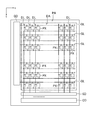
- FIG. 3 is a circuit diagram of a display device.
- FIG. 3 is a plan view showing an element structure for each pixel.
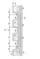
- FIG. 2 is a schematic diagram illustrating a cross section of the display device illustrated in FIG. 1. It is a detailed sectional view of a thin-film transistor.
- FIG. 3 is a detailed plan view of a thin film transistor.
- FIG. 4 is a detailed cross-sectional view illustrating a thin film transistor of a display device according to a modification of the first embodiment. It is a detailed sectional view showing the thin film transistor of the display device concerning a 2nd embodiment.
- FIG. 3 is a detailed plan view of a thin film transistor.
- FIG. 2 is a diagram illustrating an entire circuit of the display device.
- FIG. 13 is a diagram illustrating a circuit configuration of the pixel illustrated in FIG. 12.
- ⁇ above '' and ⁇ below '' are only when located directly above or directly below a certain component. Unless otherwise specified, it is intended to include the case where another component is further interposed therebetween.
- FIG. 1 is a plan view of the display device according to the first embodiment of the present invention. Since the display device is actually folded and used, FIG. 1 is a development view before the display device is folded.
- the display device includes a display DP.
- the display DP has flexibility, and can be bent in the bending corresponding area BA outside the display area DA where an image is displayed.
- An integrated circuit chip CP for driving an element for displaying an image is mounted on the display DP.
- the flexible printed circuit board FP is connected to the display DP outside the display area DA.
- the display device is, for example, an organic electroluminescence display device. In the display area DA, for example, a full-color image is displayed by combining pixels (sub-pixels) of a plurality of colors including red, green, and blue.
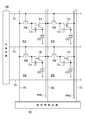
- FIG. 2 is a circuit diagram of the display device.
- the circuit has a plurality of scanning lines GL connected to the scanning circuit GD and a plurality of signal lines DL connected to the signal driving circuit SD.
- a signal drive circuit SD is arranged in the integrated circuit chip CP shown in FIG.
- An area surrounded by two adjacent scanning lines GL and two adjacent signal lines DL is one pixel PX.
- the pixel PX includes a thin film transistor TR as a driving transistor, a switching element SW, and a storage capacitor Cs.
- a gate voltage is applied to the scanning line GL, the switching element SW is turned on, a video signal is supplied from the signal line DL, and charges are accumulated in the storage capacitor Cs.
- the thin film transistor TR is turned on, and current flows from the power supply line PWL to the light emitting element OD. This current causes the light emitting element OD to emit light.
- FIG. 3 is a plan view showing the element structure of each pixel.
- a part of the scanning line GL illustrated in FIG. 2 is the gate electrode 10 of the switching element SW (for example, a thin film transistor).
- a part of the signal line DL shown in FIG. 2 is one source / drain electrode 12 (one of the source electrode and the drain electrode) of the switching element SW.
- the semiconductor layer 14 of the switching element SW is mainly made of polysilicon. Note that a thin film transistor using low-temperature polysilicon has high electron mobility, but has high off-state current and it is difficult to suppress leakage current.
- the other source / drain electrode 16 (the other of the source electrode and the drain electrode) of the switching element SW is connected to the gate electrode 18 of the thin film transistor TR.
- Part of the power supply line PWL is one source / drain electrode 20 (one of the source electrode and the drain electrode) of the thin film transistor TR.
- the gate electrode 18 of the thin film transistor TR is connected to the first capacitance electrode 22.
- the other source / drain electrode 24 (the other of the source electrode and the drain electrode) of the thin film transistor TR is connected to the second capacitance electrode 26.
- the first capacitance electrode 22 and the second capacitance electrode 26 face each other to form a storage capacitance Cs.
- the second capacitance electrode 26 is connected to the pixel electrode 28.
- the thin film transistor TR has the oxide semiconductor layer 30.
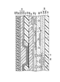
- FIG. 4 is a schematic view showing a cross section of the display device shown in FIG.
- the substrate 32 is made of polyimide. However, another resin material may be used as long as the substrate has sufficient flexibility to constitute a sheet display or a flexible display.
- a reinforcing film may be attached to the back surface of the substrate 32 via a pressure-sensitive adhesive.
- the undercoat layer 34 is laminated on the substrate 32.
- the undercoat layer 34 includes a silicon oxide film 34a and a silicon oxide film 34b.
- the lower silicon oxide film 34a is provided as a block film for preventing hydrogen atoms from diffusing into the semiconductor layer 14 of the switching element SW, in order to improve the adhesion to the substrate 32.
- the present invention is not particularly limited to this structure, and may have a laminate or a single layer.
- an additional film 36 for suppressing a change in characteristics due to intrusion of light from the back surface of the channel or providing a back gate effect is disposed.
- the additional film 36 is formed in an island shape in accordance with the location where the switching element SW is formed, and then the silicon oxide film 34b is laminated, so that the additional film 36
- the film 36 is formed so as to be sealed, the present invention is not limited to this.
- the additional film 36 may be formed first on the substrate 32, and then the undercoat layer 34 may be formed.
- the switching element SW is formed on the undercoat layer 34. Taking a polysilicon thin film transistor as an example, only an Nch transistor is shown here, but a Pch transistor may be formed at the same time.
- the semiconductor layer 14 of the switching element SW has a structure in which a low-concentration impurity region is provided between a channel region and a source / drain region.
- a silicon oxide film is used as the gate insulating film 38.
- An insulating film 40 (silicon oxide film and silicon nitride film) is laminated on the gate electrode 10. Source / drain electrodes 12 and 16 are formed so as to penetrate the insulating film 40. Here, a three-layer structure of Ti, Al and Ti is adopted.
- the switching element SW is of a top gate type and has a gate electrode 10 above the semiconductor layer 14.
- the gate electrode 18 of the thin-film transistor TR is located at the same layer position as the gate electrode 10 of the switching element SW.
- the insulating film 40 is an interlayer insulating film that covers the gate electrode 10 of the switching element SW, and is also a gate insulating film of the thin film transistor TR.
- the oxide semiconductor layer 30 is located above the gate electrode 18.
- the oxide semiconductor layer 30 is formed over the insulating film 40.
- a pair of source / drain electrodes 20 and 24 are also formed on the insulating film 40. The pair of source / drain electrodes 20 and 24 also rest on the end of the oxide semiconductor layer 30.
- the thin film transistor TR Since the thin film transistor TR has the oxide semiconductor layer 30 as a channel region, current variation can be reduced.
- the thin film transistor TR is at a layer position above the switching element SW. Therefore, since the thin film transistor TR is formed after the switching element SW, it is not affected by heat when forming the semiconductor layer 14 made of low-temperature polysilicon. Details of the thin film transistor TR will be described later (see FIG. 5).
- the first capacitance electrode 22 is also formed on the insulating film 40.
- An oxidizing agent layer 42 and a reducing agent layer 44 are stacked so as to cover the thin film transistor TR and the first capacitance electrode 22 (details will be described later).
- the second capacitance electrode 26 is formed on these.
- the oxidizing agent layer 42 and the reducing agent layer 44 are dielectrics of the storage capacitor Cs shown in FIG.
- a planarizing organic film 46 is provided so as to cover the reducing agent layer 44 and the second capacitance electrode 26.
- the planarizing organic film 46 is made of a resin such as photosensitive acrylic because it has better surface flatness than an inorganic insulating material formed by CVD (Chemical Vapor Deposition) or the like.
- the pixel electrode 28 is stacked on the flattening organic film 46.
- the pixel electrode 28 is formed as a reflective electrode, and has a three-layer structure of an indium zinc oxide film, an Ag film, and an indium zinc oxide film.
- an indium tin oxide film may be used instead of the indium zinc oxide film.
- An insulating organic film 48 called a bank (rib) and serving as a partition between adjacent pixel regions is formed on the flattening organic film 46 and on the periphery of the pixel electrode 28.
- a bank rib
- photosensitive acrylic or the like is used as in the case of the planarizing organic film 46.
- the insulating organic film 48 is preferably opened so as to expose the surface of the pixel electrode 28 as a light emitting region, and the opening end preferably has a gentle taper shape. When the opening end has a steep shape, poor coverage of the organic electroluminescent layer 50 formed thereon occurs.
- An organic electroluminescence layer 50 made of an organic material is laminated on the pixel electrode 28.
- the organic electroluminescence layer 50 may be a single layer, or may have a structure in which a hole transport layer, a light emitting layer, and an electron transport layer are sequentially stacked from the pixel electrode 28 side. These layers may be formed by vapor deposition, may be formed by application over a solvent dispersion, may be formed selectively with respect to the pixel electrode 28 (each sub-pixel), A solid pattern may be formed on the entire surface covering the area DA. In the case of solid formation, white light is obtained in all sub-pixels, and a desired color wavelength portion is extracted by a color filter (not shown).
- the counter electrode 52 is provided on the organic electroluminescent layer 50.
- the counter electrode 52 is transparent because of the top emission structure.
- the Mg layer and the Ag layer are formed as thin films that transmit light emitted from the organic electroluminescence layer 50.
- the pixel electrode 28 functions as an anode
- the counter electrode 52 functions as a cathode.
- the plurality of pixel electrodes 28, the counter electrode 52, and the organic electroluminescent layer 50 interposed between the central portion of each of the plurality of pixel electrodes 28 and the counter electrode 52 constitute the light emitting element OD.
- a sealing layer 54 is formed on the counter electrode 52.
- One of the functions of the sealing layer 54 is to prevent the organic electroluminescence layer 50 formed earlier from invading moisture from the outside, and a high gas barrier property is required.
- the sealing layer 54 has a stacked structure of a sealing organic film 54b and a pair of sealing inorganic films 54a and 54c (for example, a silicon nitride film) sandwiching the sealing organic film 54b vertically.
- the pair of sealing inorganic films 54a and 54c contact and overlap around the sealing organic film 54b.
- a silicon oxide film or an amorphous silicon layer may be provided between the sealing inorganic films 54a and 54c and the sealing organic film 54b for the purpose of improving adhesion.
- the reinforcing organic film 56 is laminated on the sealing layer 54.
- a polarizing plate 60 is attached to the reinforcing organic film 56 via an adhesive layer 58.
- the polarizing plate 60 is, for example, a circular polarizing plate.
- FIG. 5 is a detailed sectional view of the thin film transistor TR.
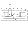
- FIG. 6 is a detailed plan view of the thin film transistor TR.
- the display device has a plurality of thin film transistors TR for controlling image display.
- Each of the plurality of thin film transistors TR is a bottom gate type.
- the thin film transistor TR has a gate electrode 18.
- the thin film transistor TR has an insulating film 40 covering the gate electrode 18.
- the thin film transistor TR has a pair of source / drain electrodes 20 and 24 (source and drain electrodes) above the insulating film 40.
- the thin film transistor TR has the oxide semiconductor layer 30 on the insulating film 40.
- the oxide semiconductor layer 30 is formed of, for example, indium / gallium / zinc / oxygen (IGZO).
- IGZO indium / gallium / zinc / oxygen
- the oxide semiconductor layer 30 has a first upper surface region R1.
- the oxidant layer 42 contacts the first upper surface region R1 of the oxide semiconductor layer 30.
- the oxidant layer 42 has a silicon oxide.
- the oxide semiconductor layer 30 includes a semiconductor portion 62 oxidized by the oxidant layer 42 from the first upper surface region R1.
- the semiconductor portion 62 becomes semiconducting because electrons are reduced by oxidation, and the transistor can operate.
- the oxidant layer 42 also rests on the pair of source / drain electrodes 20, 24 (source and drain electrodes).
- the oxide semiconductor layer 30 has the second upper surface region R2.
- the second upper surface region R2 is adjacent to both sides of the first upper surface region R1 in a direction between the pair of source / drain electrodes 20, 24 (source electrode and drain electrode).
- the reducing agent layer 44 contacts the second upper surface region R2 of the oxide semiconductor layer 30.
- the reducing agent layer 44 has a silicon nitride containing hydrogen. Hydrogen may be included depending on film formation conditions or may be originally included in silicon nitride. Hydrogen causes a reduction reaction by extracting oxygen by combining with oxygen.
- the oxide semiconductor layer 30 includes a conductive portion 64 reduced by the reducing agent layer 44 from the second upper surface region R2. The conductive portion 64 is converted into a conductor by removing oxygen by reduction and increasing the number of electrons as carriers.
- the reducing agent layer 44 is also placed on the oxidizing agent layer 42.
- the oxide semiconductor layer 30 has a pair of third upper surface regions R3 sandwiching the first upper surface region R1 and the second upper surface region R2.
- the pair of source / drain electrodes 20 and 24 respectively come in contact with and are electrically connected to the pair of third upper surface regions R3.
- the pair of source / drain electrodes 20, 24 are made of metal.
- the oxide semiconductor layer 30 is reduced by metal to be conductive.
- the oxide semiconductor layer 30 has a higher oxygen concentration and a lower hydrogen concentration in the semiconductor portion 62 than in the conductive portion 64. Further, the conductive portion 64 has a higher electrical conductivity than the semiconductor portion 62. Further, in the oxide semiconductor layer 30 immediately below the third upper surface region R3, almost no electricity flows, and electric conduction is predominantly generated in the source / drain electrodes 20 and 24.
- the second upper surface region R2 with which the reducing agent layer 44 contacts is adjacent to both sides of the first upper surface region R1 with which the oxidizing agent layer 42 contacts.
- the semiconductor portion 62 oxidized from the first upper surface region R1 is not adjacent to the pair of source / drain electrodes 20 and 24. Therefore, in the portion adjacent to the first upper surface region R1, unevenness in the thickness of the oxide semiconductor layer 30 is suppressed.
- a gate electrode 18 is formed as shown in FIG.
- An insulating film 40 is formed so as to cover the gate electrode 18.
- the oxide semiconductor layer 30 is formed over the insulating film 40.
- a pair of source / drain electrodes 20 and 24 are formed avoiding the first upper surface region R1 and the second upper surface region R2 through the formation and etching of the metal film on the oxide semiconductor layer 30.
- the pair of source / drain electrodes 20 and 24 are formed from a metal, and the etching is performed using a chlorine-based gas.
- a chlorine-based gas is used, the etching rate of a metal is close to that of a semiconductor (oxide semiconductor). Further, the thickness of the semiconductor is likely to be non-uniform in a portion adjacent to the etching mask.
- the second upper surface region R2 is adjacent to both sides of the first upper surface region R1 in a direction between the pair of source / drain electrodes 20, 24. Therefore, the pair of source / drain electrodes 20 and 24 serving as an etching mask of the oxide semiconductor layer 30 are apart from the first upper surface region R1.
- the oxidant layer 42 is formed so as to contact the first upper surface region R1 and the second upper surface region R2 of the oxide semiconductor layer 30.
- the formation of the oxidant layer 42 includes dry etching using a fluorine-based gas. When a fluorine-based gas is used, the etching rate of a metal is different from that of a semiconductor (oxide semiconductor), so that high etching selectivity can be obtained.
- the oxidant layer 42 oxidizes the oxide semiconductor layer 30 in the first upper surface region R1 and the second upper surface region R2. As a result, the semiconductor portion 62 exhibiting semiconductivity due to the reduction of electrons due to oxidation is formed.
- the oxidant layer 42 is formed so as to be placed on the pair of source / drain electrodes 20 and 24.
- the reducing agent layer 44 is formed so as to be in contact with the second upper surface region R2 of the oxide semiconductor layer 30.
- the reducing agent layer 44 is formed so as to also rest on the oxidizing agent layer 42.
- the oxide semiconductor layer 30 is reduced in the second upper surface region R2 by the reducing agent layer 44.
- the first upper surface region R1 to be oxidized by the oxidant layer 42 is not adjacent to the pair of source / drain electrodes 20 and 24. Therefore, in the portion adjacent to the first upper surface region R1, unevenness in the thickness of the oxide semiconductor layer 30 due to etching is suppressed. Since the thickness of the semiconductor portion 62 is made uniform, the characteristics as a semiconductor are stabilized. Even if the thickness of the conductive portion 64 becomes non-uniform, the conductive portion 64 does not significantly affect the characteristics of the thin film transistor TR because of the conductive portion.
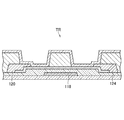
- FIG. 7 is a detailed cross-sectional view illustrating a thin film transistor TR of a display device according to a modification of the first embodiment.
- the gate electrode 118 does not overlap with the source / drain electrodes 120 and 124 (source and drain electrodes). By doing so, the capacitance formed between the gate electrode 118 and the source / drain electrodes 120 and 124 can be reduced or eliminated.
- Other contents correspond to the contents described in the first embodiment.
- FIG. 8 is a detailed cross-sectional view illustrating the thin film transistor TR of the display device according to the second embodiment.
- FIG. 9 is a detailed plan view of the thin film transistor TR.
- the pair of source / drain electrodes 220 and 224 are located so as not to overlap with the oxide semiconductor layer 230. That is, the source / drain electrodes 220 and 224 do not rest on the oxide semiconductor layer 230. Therefore, the ends of the source / drain electrodes 220 and 224 do not exist on the oxide semiconductor layer 230. Instead, a pair of metal layers 266, 268 are placed in contact with the pair of third upper surface regions R3, respectively. The pair of metal layers 266 and 268 are placed in contact with the pair of source / drain electrodes 220 and 224, respectively. The oxide semiconductor layer 230 is reduced and made conductive by the metal layers 266 and 268 in the pair of third upper surface regions R3.
- the pair of source / drain electrodes 220 and 24 are formed so as not to overlap with the oxide semiconductor layer 230. That is, when the source / drain electrodes 220 and 224 are formed by etching the metal film, an etching mask (not shown) is provided so as to cover the oxide semiconductor layer 230. Thus, the oxide semiconductor layer 230 is not etched. In particular, when the edge of the etching mask is placed on the oxide semiconductor layer 230, the film thickness becomes non-uniform in a portion adjacent thereto, but this can be avoided in the present embodiment.
- the oxidizing agent layer 242 and the reducing agent layer 244 are formed so as to avoid a pair of third upper surface regions R3 sandwiching the first upper surface region R1 and the second upper surface region R2.
- the pair of metal layers 266, 268 are formed so as to be in contact with the pair of third upper surface regions R3 and to be in contact with the pair of source / drain electrodes 220, 224, respectively.
- Other contents correspond to the contents described in the first embodiment. If the pair of metal layers 266 and 268 are formed in the same layer as the second capacitor electrode 26 shown in FIG. 4, it can be formed without increasing the process cost.
- FIG. 10 is a detailed cross-sectional view illustrating the thin film transistor TR of the display device according to the third embodiment.
- the oxide semiconductor layer 330 includes the plurality of semiconductor portions 362 at intervals. In the semiconductor portion 362, electrons are reduced by oxidation and the semiconductor portion 362 becomes semiconducting, so that the transistor can operate.
- oxide semiconductor layer 330 includes conductive portion 364 reduced from second upper surface region R2 by reducing agent layer 344.
- the conductive portion 364 is converted into a conductor by removing oxygen by reduction and increasing the number of electrons serving as carriers.
- Other contents correspond to the contents described in the first embodiment.
- FIG. 11 is a cross-sectional view of the display device according to the fourth embodiment.
- the display device is a liquid crystal display device.
- the display device has a glass substrate 470.
- An undercoat layer 434 is formed on a glass substrate 470, on which a thin film transistor TR is provided.
- the pixel electrode 428 is connected to one of the source / drain electrodes 420 and 424 (one of the source electrode and the drain electrode) of the thin film transistor TR.
- the lateral electric field method is applied to drive the liquid crystal, and a common electrode 472 is arranged below the pixel electrode 428.
- An insulating film 474 is interposed between the two.
- a slit (not shown) is formed in the pixel electrode 428.
- a first alignment film 476 is stacked so as to cover the plurality of pixel electrodes 428.
- the display device includes the opposite glass substrate 478.
- the opposite glass substrate 478 is provided with a black matrix 480 and a color filter layer 482, and is covered with an overcoat layer 484 on the lower side.
- a second alignment film 486 is stacked so as to cover the overcoat layer 484.
- the black matrix 480 is disposed between the counter glass substrate 478 and the color filter layer 482, but may be disposed between the color filter layer 482 and the overcoat layer 484. Alternatively, it may be disposed between the overcoat layer 484 and the second alignment film 486.
- a liquid crystal layer 488 is interposed between the first alignment film 476 and the second alignment film 486. The cell gap is held by a plurality of spacers (not shown).
- the display device has a backlight module 490 on the opposite side of the display surface on which an image is displayed.
- the backlight module 490 includes a light source such as an LED (Light Emitting Diode), a light guide plate, an optical film, a diffusion plate, a reflection plate, and a frame.
- the point light source is converted into a surface light source by the light guide plate.
- FIG. 12 is a diagram showing an entire circuit of the display device.
- the display device includes a display area DA for displaying an image, and a peripheral area PA outside the display area DA.
- the peripheral area PA surrounds the display area DA and has a frame shape.
- the display device includes a plurality of pixels PX in the display area DA.
- the plurality of pixels PX are arranged in a matrix in the first direction X and the second direction Y.
- one full-color pixel is constituted by three pixels PX adjacent in the first direction X.
- the display device includes a plurality of scanning lines GL and a plurality of signal lines DL.
- the scanning lines GL extend in the first direction X and are arranged at intervals in the second direction Y.
- the signal lines DL extend in the second direction Y and are arranged at intervals in the first direction X. Note that the scanning lines GL and the signal lines DL do not necessarily have to extend linearly, and some of them may be bent.
- the scanning line GL is connected to the scanning circuit GD.
- the signal line DL is connected to the signal drive circuit SD.
- FIG. 13 is a diagram showing a circuit configuration of the pixel PX shown in FIG.
- the pixel PX includes a thin film transistor TR arranged near a position where the scanning line GL and the signal line DL intersect.
- the thin film transistor TR is electrically connected to the scanning line GL and the signal line DL.
- the scanning line GL is connected to the thin film transistors TR in each of the pixels PX arranged in the first direction X shown in FIG.
- the signal line DL is connected to the thin film transistor TR in each of the pixels PX arranged in the second direction Y shown in FIG.
- the pixel electrode 428 is arranged in a region surrounded by the scanning line GL and the signal line DL.
- the thin film transistor TR is electrically connected to the pixel electrode 428.
- the pixel electrode 428 faces the common electrode 472, and drives the liquid crystal layer 488 by an electric field generated between the pixel electrode 428 and the common electrode 472.
- the common electrode 472 is connected to the common drive circuit CD shown in FIG. 12 and is arranged over a plurality of pixels PX. Both ends of the storage capacitor Cs are electrically connected to the common electrode 472 and the pixel electrode 428.
- the present invention is not limited to the embodiments described above, and various modifications are possible.
- the configuration described in the embodiment can be replaced with a configuration having substantially the same configuration, a configuration having the same operation and effect, or a configuration capable of achieving the same object.
Landscapes
- Engineering & Computer Science (AREA)
- Microelectronics & Electronic Packaging (AREA)
- Physics & Mathematics (AREA)
- General Physics & Mathematics (AREA)
- Theoretical Computer Science (AREA)
- Devices For Indicating Variable Information By Combining Individual Elements (AREA)
- Manufacturing & Machinery (AREA)
- Liquid Crystal (AREA)
- Electroluminescent Light Sources (AREA)
- Thin Film Transistor (AREA)
Abstract
画像表示の制御をするための薄膜トランジスタ(TR)は、ボトムゲート型であって、ゲート電極(18)と、ゲート電極(18)を覆う絶縁膜(40)と、絶縁膜(40)の上にある酸化物半導体層(30)と、酸化物半導体層(30)の第1上面領域(R1)に接触する酸化剤層(42)と、酸化物半導体層(30)の第2上面領域(R2)に接触する還元剤層(44)と、絶縁膜(40)の上方にあるソース電極及びドレイン電極(20,24)と、を有する。第2上面領域(R2)は、ソース電極及びドレイン電極(20,24)の間の方向で、第1上面領域(R1)の両側のそれぞれに隣接する。酸化物半導体層(30)は、酸化剤層(42)直下の半導体部(62)と、還元剤層(44)直下の導電部(64)と、を含む。
Description
本発明は、表示装置及びその製造方法に関する。
低温ポリシリコンを使用した薄膜トランジスタ(TFT)は、駆動能力が高く、キャリア移動度が高いので、有機エレクトロルミネセンスディスプレイや高精細の液晶ディスプレイに用いられているが、オフ電流が高く、リーク電流の抑制が困難である。そこで、近年、酸化物半導体を使用したTFTが開発されている(特許文献1及び2)。
ボトムゲート型のTFTでは、半導体層の上で金属膜をエッチングしてソース電極及びドレイン電極を形成する。金属のエッチングで多用される塩素ガスは、金属と半導体のエッチング選択比が小さいので、半導体層の無用なエッチングが進行する。特に、ソース電極及びドレイン電極に隣接する部分では、半導体層の膜厚が大きく不均一になる。酸化物半導体TFTは、オフ電流が低いが、キャリア移動度が低いため、不均一な膜厚は特性に与える影響が大きい。
本発明は、酸化物半導体層の膜厚が不均一化されることの抑制を目的とする。
本発明に係る表示装置は、画像表示の制御をするための複数の薄膜トランジスタを有し、前記複数の薄膜トランジスタのそれぞれは、ボトムゲート型であって、ゲート電極と、前記ゲート電極を覆うゲート絶縁膜と、前記ゲート絶縁膜の上にある酸化物半導体層と、前記酸化物半導体層の第1上面領域に接触するシリコン酸化物と、前記酸化物半導体層の第2上面領域に接触するシリコン窒化物と、前記ゲート絶縁膜の上方にあるソース電極及びドレイン電極と、を有し、前記第2上面領域は、前記ソース電極及び前記ドレイン電極の間の方向で、前記第1上面領域の両側のそれぞれに隣接し、前記酸化物半導体層は、前記シリコン酸化物直下の半導体部と、前記シリコン窒化物直下の導電部と、を含むことを特徴とする。
本発明によれば、還元剤層が接触する第2上面領域は、酸化剤層が接触する第1上面領域の両側のそれぞれに隣接している。第1上面領域から酸化された半導体部は、ソース電極及びドレイン電極に隣接しない。そのため、第1上面領域に隣接する部分では、酸化物半導体層の膜厚の不均一化が抑えられている。
本発明に係る表示装置の製造方法は、ゲート電極を形成する工程と、前記ゲート電極を覆うようにゲート絶縁膜を形成する工程と、前記ゲート絶縁膜の上に酸化物半導体層を形成する工程と、前記酸化物半導体層の上での成膜及びエッチングを経て、前記酸化物半導体層の第1上面領域及び第2上面領域を避けて、ソース電極及びドレイン電極を形成する工程と、前記酸化物半導体層の前記第1上面領域に接触するように酸化剤層を形成し、前記第1上面領域で前記酸化物半導体層を酸化する工程と、前記酸化物半導体層の前記第2上面領域に接触するように還元剤層を形成し、前記第2上面領域で前記酸化物半導体層を還元する工程と、を含み、前記第2上面領域は、前記ソース電極及び前記ドレイン電極の間の方向で、前記第1上面領域の両側のそれぞれに隣接することを特徴とする。
本発明によれば、還元剤層が接触する第2上面領域は、酸化剤層が接触する第1上面領域の両側のそれぞれに隣接している。酸化剤層によって酸化するための第1上面領域は、ソース電極及びドレイン電極に隣接しない。そのため、第1上面領域に隣接する部分では、エッチングによる酸化物半導体層の膜厚の不均一化を抑えることができる。
以下、本発明の実施形態について図面を参照して説明する。但し、本発明は、その要旨を逸脱しない範囲において様々な態様で実施することができ、以下に例示する実施形態の記載内容に限定して解釈されるものではない。
図面は、説明をより明確にするため、実際の態様に比べ、各部の幅、厚さ、形状等について模式的に表される場合があるが、あくまで一例であって、本発明の解釈を限定するものではない。本明細書と各図において、既出の図に関して説明したものと同様の機能を備えた要素には、同一の符号を付して、重複する説明を省略することがある。
さらに、本発明の詳細な説明において、ある構成物と他の構成物の位置関係を規定する際、「上に」「下に」とは、ある構成物の直上あるいは直下に位置する場合のみでなく、特に断りの無い限りは、間にさらに他の構成物を介在する場合を含むものとする。
[第1の実施形態]
図1は、本発明の第1の実施形態に係る表示装置の平面図である。表示装置は、実際には、折り曲げて使用するので、図1は、表示装置を折り曲げる前の展開図である。表示装置は、ディスプレイDPを含む。ディスプレイDPは、可撓性を有しており、画像が表示される表示領域DAの外側にある屈曲対応領域BAで折り曲げられるようになっている。ディスプレイDPには、画像を表示するための素子を駆動するための集積回路チップCPが搭載されている。ディスプレイDPには、表示領域DAの外側で、フレキシブルプリント基板FPが接続されている。表示装置は、例えば、有機エレクトロルミネセンス表示装置である。表示領域DAでは、例えば、赤、緑及び青からなる複数色の画素(サブピクセル)を組み合わせて、フルカラー画像が表示される。
図1は、本発明の第1の実施形態に係る表示装置の平面図である。表示装置は、実際には、折り曲げて使用するので、図1は、表示装置を折り曲げる前の展開図である。表示装置は、ディスプレイDPを含む。ディスプレイDPは、可撓性を有しており、画像が表示される表示領域DAの外側にある屈曲対応領域BAで折り曲げられるようになっている。ディスプレイDPには、画像を表示するための素子を駆動するための集積回路チップCPが搭載されている。ディスプレイDPには、表示領域DAの外側で、フレキシブルプリント基板FPが接続されている。表示装置は、例えば、有機エレクトロルミネセンス表示装置である。表示領域DAでは、例えば、赤、緑及び青からなる複数色の画素(サブピクセル)を組み合わせて、フルカラー画像が表示される。
図2は、表示装置の回路図である。回路は、走査回路GDに接続される複数の走査線GLと、信号駆動回路SDに接続される複数の信号線DLを有する。図1に示す集積回路チップCP内に信号駆動回路SDが配置されている。隣接する2つの走査線GLと隣接する2つの信号線DLとで囲まれる領域が1つの画素PXである。画素PXは、駆動トランジスタとしての薄膜トランジスタTR及びスイッチング素子SWと保持容量Csを含む。走査線GLにゲート電圧が印加されることにより、スイッチング素子SWがON状態となり、信号線DLから映像信号が供給され、保持容量Csに電荷が蓄積される。保持容量Csに電荷が蓄積されることにより、薄膜トランジスタTRがON状態となり、電源線PWLから発光素子ODに電流が流れる。この電流により発光素子ODが発光する。
図3は、画素ごとの素子構造を示す平面図である。図2に示す走査線GLの一部は、スイッチング素子SW(例えば薄膜トランジスタ)のゲート電極10である。図2に示す信号線DLの一部は、スイッチング素子SWの一方のソース・ドレイン電極12(ソース電極及びドレイン電極の一方)である。スイッチング素子SWの半導体層14は、ポリシリコンを主原料としている。なお、低温ポリシリコンを使用した薄膜トランジスタは、電子移動度が高いが、オフ電流が高くリーク電流の抑制が難しい。
スイッチング素子SWの他のソース・ドレイン電極16(ソース電極及びドレイン電極の他方)は、薄膜トランジスタTRのゲート電極18に接続されている。電源線PWLの一部は、薄膜トランジスタTRの一方のソース・ドレイン電極20(ソース電極及びドレイン電極の一方)である。
薄膜トランジスタTRのゲート電極18は、第1容量電極22に接続されている。薄膜トランジスタTRの他方のソース・ドレイン電極24(ソース電極及びドレイン電極の他方)は、第2容量電極26に接続されている。第1容量電極22及び第2容量電極26は相互に対向して、保持容量Csを構成する。第2容量電極26は、画素電極28に接続されている。薄膜トランジスタTRは酸化物半導体層30を有する。
図4は、図1に示す表示装置の断面を示す模式図である。基板32は、ポリイミドからなる。ただし、シートディスプレイ又はフレキシブルディスプレイを構成するために十分な可撓性を有する基材であれば他の樹脂材料を用いてもよい。基板32の裏面には、感圧接着剤を介して補強フィルムを貼り付けてもよい。
基板32上に、アンダーコート層34が積層されている。アンダーコート層34は、シリコン酸化膜34a及びシリコン酸化膜34bを含む。下層のシリコン酸化膜34aは、基板32との密着性向上のため、上層のシリコン酸化膜34bは、水素原子がスイッチング素子SWの半導体層14に拡散しないようにするブロック膜として、それぞれ設けられるが、特にこの構造に限定するものではなく、さらに積層があってもよいし、単層であってもよい。
スイッチング素子SWの下方には、チャネル裏面からの光の侵入等による特性変化を抑制したり、バックゲート効果を付与したりするための付加膜36が配置されている。ここでは、シリコン酸化膜34aを形成した後、スイッチング素子SWが形成される箇所に合わせて付加膜36を島状に形成し、その後シリコン酸化膜34bを積層することで、アンダーコート層34に付加膜36を封入するように形成しているが、この限りではなく、基板32上にまず付加膜36を形成し、その後にアンダーコート層34を形成してもよい。
アンダーコート層34上にスイッチング素子SWが形成されている。ポリシリコン薄膜トランジスタを例に挙げて、ここではNchトランジスタのみを示しているが、Pchトランジスタを同時に形成してもよい。スイッチング素子SWの半導体層14は、チャネル領域とソース・ドレイン領域との間に、低濃度不純物領域を設けた構造を採る。ゲート絶縁膜38としてはここではシリコン酸化膜を用いる。
ゲート電極10の上に、絶縁膜40(シリコン酸化膜及びシリコン窒化膜)が積層されている。絶縁膜40を貫通するように、ソース・ドレイン電極12,16が形成されている。ここでは、Ti、Al及びTiの三層積層構造を採用する。スイッチング素子SWは、トップゲート型であって、半導体層14の上方にゲート電極10を有する。
薄膜トランジスタTRのゲート電極18は、スイッチング素子SWのゲート電極10と同じ層位置にある。絶縁膜40は、スイッチング素子SWのゲート電極10を覆う層間絶縁膜であるとともに、薄膜トランジスタTRのゲート絶縁膜でもある。ゲート電極18の上方に酸化物半導体層30がある。酸化物半導体層30は、絶縁膜40の上に形成されている。一対のソース・ドレイン電極20,24(ソース電極及びドレイン電極)も絶縁膜40の上に形成されている。一対のソース・ドレイン電極20,24は、酸化物半導体層30の端部にも載る。
薄膜トランジスタTRは、酸化物半導体層30をチャネル領域として有するので、電流バラツキを小さくすることができる。薄膜トランジスタTRは、スイッチング素子SWよりも上の層位置にある。したがって、薄膜トランジスタTRは、スイッチング素子SWよりも後に形成するので、低温ポリシリコンからなる半導体層14を形成するときの熱による影響を受けない。薄膜トランジスタTRの詳細は後述する(図5参照)。
第1容量電極22も絶縁膜40の上に形成されている。薄膜トランジスタTR及び第1容量電極22を覆うように、酸化剤層42及び還元剤層44が積層されている(詳細は後述)。これらの上に第2容量電極26が形成されている。酸化剤層42及び還元剤層44は、図2に示す保持容量Csの誘電体になっている。
還元剤層44及び第2容量電極26を覆うように平坦化有機膜46が設けられている。平坦化有機膜46は、CVD(Chemical Vapor Deposition)等により形成される無機絶縁材料に比べ、表面の平坦性に優れることから、感光性アクリル等の樹脂が用いられる。
平坦化有機膜46の上に画素電極28が積層されている。画素電極28は、反射電極として形成され、酸化インジウム亜鉛膜、Ag膜、酸化インジウム亜鉛膜の三層積層構造になっている。ここで、酸化インジウム亜鉛膜に代わって酸化インジウムスズ膜を用いてもよい。
平坦化有機膜46の上であって画素電極28の周縁に載るように、バンク(リブ)と呼ばれて隣同士の画素領域の隔壁となる絶縁有機膜48が形成されている。絶縁有機膜48としては平坦化有機膜46と同じく感光性アクリル等が用いられる。絶縁有機膜48は、画素電極28の表面を発光領域として露出するように開口され、その開口端はなだらかなテーパー形状となるのが好ましい。開口端が急峻な形状になっていると、その上に形成される有機エレクトロルミネセンス層50のカバレッジ不良を生ずる。
画素電極28の上に、有機材料からなる有機エレクトロルミネセンス層50が積層されている。有機エレクトロルミネセンス層50は、単層であってもよいが、画素電極28側から順に、正孔輸送層、発光層及び電子輸送層が積層された構造であってもよい。これらの層は、蒸着によって形成してもよいし、溶媒分散の上での塗布によって形成してもよく、画素電極28(各サブ画素)に対して選択的に形成してもよいし、表示領域DAを覆う全面にベタ形成されてもよい。ベタ形成の場合は、全サブ画素において白色光を得て、カラーフィルタ(図示せず)によって所望の色波長部分を取り出す構成になる。
有機エレクトロルミネセンス層50の上に、対向電極52が設けられている。ここでは、トップエミッション構造としているため、対向電極52は透明である。例えば、Mg層及びAg層を、有機エレクトロルミネセンス層50からの出射光が透過する程度の薄膜として形成する。前述の有機エレクトロルミネセンス層50の形成順序に従うと、画素電極28が陽極となり、対向電極52が陰極となる。複数の画素電極28と、対向電極52と、複数の画素電極28のそれぞれの中央部と対向電極52の間に介在する有機エレクトロルミネセンス層50と、で発光素子ODが構成される。
対向電極52の上に、封止層54が形成されている。封止層54は、先に形成した有機エレクトロルミネセンス層50を、外部からの水分侵入を防止することを機能の一としており、高いガスバリア性が要求される。封止層54は、封止有機膜54b及びこれを上下で挟む一対の封止無機膜54a,54c(例えばシリコン窒化膜)の積層構造になっている。一対の封止無機膜54a,54cは、封止有機膜54bの周囲で接触して重なる。封止無機膜54a,54cと封止有機膜54bとの間には、密着性向上を目的の一として、シリコン酸化膜やアモルファスシリコン層を設けてもよい。封止層54には、補強有機膜56が積層されている。補強有機膜56には、粘着層58を介して、偏光板60が貼り付けられている。偏光板60は、例えば円偏光板である。
図5は、薄膜トランジスタTRの詳細断面図である。図6は、薄膜トランジスタTRの詳細平面図である。
表示装置は、画像表示の制御をするための複数の薄膜トランジスタTRを有する。複数の薄膜トランジスタTRのそれぞれは、ボトムゲート型である。薄膜トランジスタTRは、ゲート電極18を有する。薄膜トランジスタTRは、ゲート電極18を覆う絶縁膜40を有する。薄膜トランジスタTRは、絶縁膜40の上方にある一対のソース・ドレイン電極20,24(ソース電極及びドレイン電極)を有する。
薄膜トランジスタTRは、絶縁膜40の上にある酸化物半導体層30を有する。酸化物半導体層30は、例えばインジウム・ガリウム・亜鉛・酸素(IGZO)から形成されている。このような薄膜トランジスタTRは、オフ電流が低い特性を有する。
酸化物半導体層30は第1上面領域R1を有する。酸化物半導体層30の第1上面領域R1に、酸化剤層42が接触する。酸化剤層42は、シリコン酸化物を有する。酸化物半導体層30は、第1上面領域R1から酸化剤層42によって酸化された半導体部62を含む。半導体部62は、酸化によって電子が減って半導体性を示すようになり、トランジスタの動作が可能になる。酸化剤層42は、一対のソース・ドレイン電極20,24(ソース電極及びドレイン電極)にも載る。
酸化物半導体層30は第2上面領域R2を有する。第2上面領域R2は、一対のソース・ドレイン電極20,24(ソース電極及びドレイン電極)の間の方向で、第1上面領域R1の両側のそれぞれに隣接する。酸化物半導体層30の第2上面領域R2に、還元剤層44が接触する。還元剤層44は、水素を含むシリコン窒化物を有する。水素は、成膜条件によって含まれる場合やシリコン窒化物に元々含まれる場合がある。水素は、酸素と結合することで酸素を引き抜く還元反応を起こす。酸化物半導体層30は、第2上面領域R2から還元剤層44によって還元された導電部64を含む。導電部64は、還元によって酸素が抜けて、キャリアである電子が増えて導体化している。還元剤層44は、酸化剤層42にも載る。
酸化物半導体層30は、第1上面領域R1及び第2上面領域R2を挟む一対の第3上面領域R3を有する。一対のソース・ドレイン電極20,24は、それぞれ、一対の第3上面領域R3に接触して載り、電気的に接続する。一対のソース・ドレイン電極20,24は、金属からなる。酸化物半導体層30は、一対の第3上面領域R3では、金属によって還元されて導電化している。
酸化物半導体層30は、半導体部62においては導電部64に比べて酸素濃度が高くなっており、水素濃度が低くなっている。さらに半導体部62に比べて導電部64は電気伝導度が高い。さらに第3上面領域R3直下の酸化物半導体層30においては、電気が殆ど流れず、ソース・ドレイン電極20、24にて支配的に電気伝導が発生する。
酸化物半導体層30は、半導体部62においては導電部64に比べて酸素濃度が高くなっており、水素濃度が低くなっている。さらに半導体部62に比べて導電部64は電気伝導度が高い。さらに第3上面領域R3直下の酸化物半導体層30においては、電気が殆ど流れず、ソース・ドレイン電極20、24にて支配的に電気伝導が発生する。
本実施形態によれば、還元剤層44が接触する第2上面領域R2は、酸化剤層42が接触する第1上面領域R1の両側のそれぞれに隣接している。第1上面領域R1から酸化された半導体部62は、一対のソース・ドレイン電極20,24に隣接しない。そのため、第1上面領域R1に隣接する部分では、酸化物半導体層30の膜厚の不均一化が抑えられている。
[表示装置の製造方法]
表示装置の製造方法では、図5に示すように、ゲート電極18を形成する。ゲート電極18を覆うように絶縁膜40を形成する。絶縁膜40の上に酸化物半導体層30を形成する。
表示装置の製造方法では、図5に示すように、ゲート電極18を形成する。ゲート電極18を覆うように絶縁膜40を形成する。絶縁膜40の上に酸化物半導体層30を形成する。
酸化物半導体層30の上での金属膜の成膜及びそのエッチングを経て、第1上面領域R1及び第2上面領域R2を避けて、一対のソース・ドレイン電極20,24を形成する。一対のソース・ドレイン電極20,24は金属から形成し、エッチングは、塩素系ガスを使用して行う。塩素系ガスを使用すると、金属のエッチングレートと、半導体(酸化物半導体)のエッチングレートが近い。また、半導体は、エッチングマスクに隣接する部分では膜厚が不均一になりやすい。しかし、第2上面領域R2は、一対のソース・ドレイン電極20,24の間の方向で、第1上面領域R1の両側のそれぞれに隣接する。したがって、酸化物半導体層30のエッチングマスクとなる一対のソース・ドレイン電極20,24は、第1上面領域R1から離れている。
酸化物半導体層30の第1上面領域R1および第2上面領域R2に接触するように酸化剤層42を形成する。酸化剤層42の形成は、フッ素系ガスを使用したドライエッチングを含む。フッ素系ガスを使用すると、金属のエッチングレートと、半導体(酸化物半導体)のエッチングレートが異なるので、高いエッチング選択性を得ることができる。
酸化剤層42によって、第1上面領域R1および第2上面領域R2で酸化物半導体層30が酸化される。これにより、酸化によって電子が減って半導体性を示す半導体部62が形成される。酸化剤層42は、一対のソース・ドレイン電極20,24にも載るように形成する。
酸化物半導体層30の第2上面領域R2に接触するように還元剤層44を形成する。還元剤層44は、酸化剤層42にも載るように形成する。還元剤層44によって、第2上面領域R2で酸化物半導体層30が還元される。
本実施形態によれば、酸化剤層42によって酸化するための第1上面領域R1は、一対のソース・ドレイン電極20,24に隣接しない。そのため、第1上面領域R1に隣接する部分では、エッチングによる酸化物半導体層30の膜厚の不均一化が抑えられる。半導体部62においては膜厚が均一化されるため、半導体としての特性が安定する。導電部64は膜厚が不均一となっても、導体化されている箇所のためにそれほど薄膜トランジスタTRの特性の悪影響を与えない。
[第1の実施形態の変形例]
図7は、第1の実施形態の変形例に係る表示装置の薄膜トランジスタTRを示す詳細断面図である。この例では、ゲート電極118は、ソース・ドレイン電極120,124(ソース電極及びドレイン電極)にオーバーラップしない。こうすることで、ゲート電極118とソース・ドレイン電極120,124の間に形成される容量を小さく又は無くすことができる。その他の内容は、第1の実施形態で説明した内容が該当する。
図7は、第1の実施形態の変形例に係る表示装置の薄膜トランジスタTRを示す詳細断面図である。この例では、ゲート電極118は、ソース・ドレイン電極120,124(ソース電極及びドレイン電極)にオーバーラップしない。こうすることで、ゲート電極118とソース・ドレイン電極120,124の間に形成される容量を小さく又は無くすことができる。その他の内容は、第1の実施形態で説明した内容が該当する。
[第2の実施形態]
図8は、第2の実施形態に係る表示装置の薄膜トランジスタTRを示す詳細断面図である。図9は、薄膜トランジスタTRの詳細平面図である。
図8は、第2の実施形態に係る表示装置の薄膜トランジスタTRを示す詳細断面図である。図9は、薄膜トランジスタTRの詳細平面図である。
本実施形態では、一対のソース・ドレイン電極220,224(ソース電極及びドレイン電極)は、酸化物半導体層230との重なりを避けて位置している。つまり、ソース・ドレイン電極220,224は、酸化物半導体層230に載らない。そのため、ソース・ドレイン電極220,224の端が酸化物半導体層230の上に存在しない。その代わりに、一対の金属層266,268が、一対の第3上面領域R3にそれぞれ接触して載る。また、一対の金属層266,268は、それぞれ、一対のソース・ドレイン電極220,224に接触して載る。酸化物半導体層230は、一対の第3上面領域R3では、金属層266,268によって還元されて導電化されている。
本実施形態に係る表示装置の製造方法では、一対のソース・ドレイン電極220,24は、酸化物半導体層230との重なりを避けて形成する。つまり、金属膜のエッチングによってソース・ドレイン電極220,224を形成するときに、図示しないエッチングマスクを、酸化物半導体層230を覆うように配置する。これにより、酸化物半導体層230がエッチングされない。特に、エッチングマスクの端が酸化物半導体層230に載ると、その隣接した部分で膜厚が不均一になるが、本実施形態ではそれを避けることができる。
酸化剤層242及び還元剤層244は、第1上面領域R1及び第2上面領域R2を挟む一対の第3上面領域R3を避けて形成する。一対の金属層266,268は、それぞれ、一対の第3上面領域R3に接触して載り、一対のソース・ドレイン電極220,224にそれぞれ接触して載るように形成する。その他の内容は、第1の実施形態で説明した内容が該当する。尚、一対の金属層266、268は図4に示された第2容量電極26と同層で形成するとプロセスコストを上げないで形成することが可能となる。
[第3の実施形態]
図10は、第3の実施形態に係る表示装置の薄膜トランジスタTRを示す詳細断面図である。
図10は、第3の実施形態に係る表示装置の薄膜トランジスタTRを示す詳細断面図である。
本実施形態では、一対のソース・ドレイン電極320,324の間の方向に、相互に分離された複数の第1上面領域R1がある。複数の第1上面領域R1のそれぞれに酸化剤層342が載って、酸化物半導体層330が酸化されている。これにより、酸化物半導体層330は、相互に間隔をあけて、複数の半導体部362を含む。半導体部362は、酸化によって電子が減って半導体性を示すようになり、トランジスタの動作が可能になる。
複数の第1上面領域R1の間に第2上面領域R2の一部がある。隣同士の第1上面領域R1の間で、第2上面領域R2に還元剤層344が載って、酸化物半導体層330が還元される。これにより、酸化物半導体層330は、第2上面領域R2から還元剤層344によって還元された導電部364を含む。導電部364は、還元によって酸素が抜けて、キャリアである電子が増えて導体化している。その他の内容は、第1の実施形態で説明した内容が該当する。
[第4の実施形態]
図11は、第4の実施形態に係る表示装置の断面図である。表示装置は、液晶表示装置である。
図11は、第4の実施形態に係る表示装置の断面図である。表示装置は、液晶表示装置である。
表示装置は、ガラス基板470を有する。ガラス基板470の上にアンダーコート層434が形成され、その上に薄膜トランジスタTRがある。薄膜トランジスタTRの一方のソース・ドレイン電極420,424(ソース電極及びドレイン電極の一方)に画素電極428が接続されている。液晶の駆動には、横電界方式が適用されており、画素電極428の下方に共通電極472が配置されている。両者間には絶縁膜474が介在する。画素電極428には、図示しないスリットが形成されている。複数の画素電極428を覆うように第1配向膜476が積層する。
表示装置は、対向ガラス基板478を有する。対向ガラス基板478には、ブラックマトリクス480及びカラーフィルタ層482が設けられ、下側においてオーバーコート層484で覆われている。オーバーコート層484を覆うように、第2配向膜486が積層する。なお、図示した例では、ブラックマトリクス480は、対向ガラス基板478とカラーフィルタ層482との間に配置されているが、カラーフィルタ層482とオーバーコート層484との間に配置されていてもよいし、オーバーコート層484と第2配向膜486との間に配置されていてもよい。第1配向膜476と第2配向膜486の間に液晶層488が介在する。セルギャップは、図示しない複数のスペーサによって保持される。
表示装置は、画像が表示される表示面の反対側に、バックライトモジュール490を有する。バックライトモジュール490は、LED(Light Emitting Diode)などの光源、導光板、光学フィルム、拡散板、反射板及びフレームを含む。点光源が導光板によって面光源に変換される。
図12は、表示装置の全体回路を示す図である。表示装置は、画像を表示する表示領域DAと、表示領域DAの外側の周辺領域PAと、を備えている。例えば、周辺領域PAは、表示領域DAを囲み、額縁状の形状を有している。表示装置は、表示領域DAにおいて、複数の画素PXを備えている。複数の画素PXは、第1方向X及び第2方向Yにマトリクス状に配置されている。本実施形態においては、第1方向Xに隣り合う3個の画素PXで1つのフルカラー画素を構成する。
表示装置は、複数の走査線GL、複数の信号線DLを備えている。走査線GLは、第1方向Xに延出し、第2方向Yに間隔を置いて配置されている。信号線DLは、第2方向Yに延出し、第1方向Xに間隔を置いて配置されている。なお、走査線GL及び信号線DLは、必ずしも直線的に延出していなくてもよく、それらの一部が屈曲していてもよい。走査線GLは、走査回路GDに接続されている。信号線DLは、信号駆動回路SDに接続されている。
図13は、図12に示す画素PXの回路構成を示す図である。画素PXは、走査線GL及び信号線DLが交差する位置近傍に配置された薄膜トランジスタTRを備えている。薄膜トランジスタTRは、走査線GL及び信号線DLと電気的に接続されている。走査線GLは、図12に示す第1方向Xに並んだ画素PXの各々における薄膜トランジスタTRと接続されている。信号線DLは、図12に示す第2方向Yに並んだ画素PXの各々における薄膜トランジスタTRと接続されている。
画素電極428は、走査線GLと信号線DLとで囲まれた領域に配置されている。薄膜トランジスタTRは、画素電極428と電気的に接続されている。画素電極428は、共通電極472と対向し、画素電極428と共通電極472との間に生じる電界によって液晶層488を駆動する。共通電極472は、図12に示す共通駆動回路CDに接続されて、複数の画素PXにわたって配置されている。保持容量Csの両端は、共通電極472及び画素電極428に電気的に接続する。
本発明は、上述した実施形態に限定されるものではなく種々の変形が可能である。例えば、実施形態で説明した構成は、実質的に同一の構成、同一の作用効果を奏する構成又は同一の目的を達成することができる構成で置き換えることができる。
Claims (17)
- 画像表示の制御をするための複数の薄膜トランジスタを有し、
前記複数の薄膜トランジスタのそれぞれは、ボトムゲート型であって、
ゲート電極と、
前記ゲート電極を覆うゲート絶縁膜と、
前記ゲート絶縁膜の上にある酸化物半導体層と、
前記酸化物半導体層の第1上面領域に接触するシリコン酸化物と、
前記酸化物半導体層の第2上面領域に接触するシリコン窒化物と、
前記ゲート絶縁膜の上方にあるソース電極及びドレイン電極と、
を有し、
前記第2上面領域は、前記ソース電極及び前記ドレイン電極の間の方向で、前記第1上面領域の両側のそれぞれに隣接し、
前記酸化物半導体層は、前記シリコン酸化物直下の半導体部と、前記シリコン窒化物直下の導電部と、を含むことを特徴とする表示装置。 - 請求項1に記載された表示装置において、
前記シリコン酸化物は酸化剤層であり、
前記シリコン窒化物は水素を含む還元剤層であることを特徴とする表示装置。 - 請求項1に記載された表示装置において、
前記酸化物半導体層は、前記第1上面領域及び前記第2上面領域を挟む一対の第3上面領域を有し、
前記ソース電極及び前記ドレイン電極は、それぞれ、前記一対の第3上面領域に電気的に接続することを特徴とする表示装置。 - 請求項3に記載された表示装置において、
前記ソース電極及び前記ドレイン電極は、それぞれ、前記一対の第3上面領域に接触して載ることを特徴とする表示装置。 - 請求項4に記載された表示装置において、
前記ソース電極及び前記ドレイン電極は、金属からなり、
前記酸化物半導体層は、前記一対の第3上面領域では、前記金属によって還元されることを特徴とする表示装置。 - 請求項3に記載された表示装置において、
前記ソース電極及び前記ドレイン電極は、前記酸化物半導体層との重なりを避けて位置し、
前記一対の第3上面領域にそれぞれ接触して載り、前記ソース電極及び前記ドレイン電極にそれぞれ接触して載る一対の金属層をさらに有することを特徴とする表示装置。 - 請求項6に記載された表示装置において、
前記酸化物半導体層は、前記一対の第3上面領域では、前記金属層によって還元されることを特徴とする表示装置。 - 請求項1から7のいずれか1項に記載された表示装置において、
前記第1上面領域は、前記ソース電極及び前記ドレイン電極の間の前記方向で相互に分離された複数の第1上面領域を含み、
前記複数の第1上面領域の間に前記第2上面領域の一部があることを特徴とする表示装置。 - 請求項1から7のいずれか1項に記載された表示装置において、
前記シリコン酸化物は、前記ソース電極及び前記ドレイン電極にも載っていることを特徴とする表示装置。 - 請求項9に記載された表示装置において、
前記シリコン窒化物は、前記シリコン酸化物にも載っていることを特徴とする表示装置。 - 請求項1から7のいずれか1項に記載された表示装置において、
前記ゲート電極は、前記ソース電極及び前記ドレイン電極のいずれにもオーバーラップしないことを特徴とする表示装置。 - ゲート電極を形成する工程と、
前記ゲート電極を覆うようにゲート絶縁膜を形成する工程と、
前記ゲート絶縁膜の上に酸化物半導体層を形成する工程と、
前記酸化物半導体層の上での成膜及びエッチングを経て、前記酸化物半導体層の第1上面領域及び第2上面領域を避けて、ソース電極及びドレイン電極を形成する工程と、
前記酸化物半導体層の前記第1上面領域に接触するように酸化剤層を形成し、前記第1上面領域で前記酸化物半導体層を酸化する工程と、
前記酸化物半導体層の前記第2上面領域に接触するように還元剤層を形成し、前記第2上面領域で前記酸化物半導体層を還元する工程と、
を含み、
前記第2上面領域は、前記ソース電極及び前記ドレイン電極の間の方向で、前記第1上面領域の両側のそれぞれに隣接することを特徴とする表示装置の製造方法。 - 請求項12に記載された表示装置の製造方法において、
前記エッチングは、塩素系ガスを使用して行うことを特徴とする表示装置の製造方法。 - 請求項12に記載された表示装置の製造方法において、
前記酸化剤層の形成は、フッ素系ガスを使用したドライエッチングを含むことを特徴とする表示装置の製造方法。 - 請求項12に記載された表示装置の製造方法において、
前記酸化剤層を形成する工程で、前記酸化剤層を、前記ソース電極及び前記ドレイン電極にも載るように形成することを特徴とする表示装置の製造方法。 - 請求項15に記載された表示装置の製造方法において、
前記還元剤層を形成する工程で、前記還元剤層を、前記酸化剤層にも載るように形成することを特徴とする表示装置の製造方法。 - 請求項12から16のいずれか1項に記載された表示装置の製造方法において、
前記ソース電極及び前記ドレイン電極を、前記酸化物半導体層との重なりを避けて形成し、
前記酸化剤層及び前記還元剤層を、前記第1上面領域及び前記第2上面領域を挟む一対の第3上面領域を避けて形成し、
前記一対の第3上面領域にそれぞれ接触して載り、前記ソース電極及び前記ドレイン電極にそれぞれ接触して載るように、一対の金属層を形成する工程をさらに含むことを特徴とする表示装置の製造方法。
Priority Applications (2)
| Application Number | Priority Date | Filing Date | Title |
|---|---|---|---|
| CN201980047944.5A CN112424918A (zh) | 2018-08-10 | 2019-07-09 | 显示装置及其制造方法 |
| US17/161,709 US20210151536A1 (en) | 2018-08-10 | 2021-01-29 | Display device and manufacturing method thereof |
Applications Claiming Priority (2)
| Application Number | Priority Date | Filing Date | Title |
|---|---|---|---|
| JP2018151624A JP2020027862A (ja) | 2018-08-10 | 2018-08-10 | 表示装置及びその製造方法 |
| JP2018-151624 | 2018-08-10 |
Related Child Applications (1)
| Application Number | Title | Priority Date | Filing Date |
|---|---|---|---|
| US17/161,709 Continuation US20210151536A1 (en) | 2018-08-10 | 2021-01-29 | Display device and manufacturing method thereof |
Publications (1)
| Publication Number | Publication Date |
|---|---|
| WO2020031587A1 true WO2020031587A1 (ja) | 2020-02-13 |
Family
ID=69415463
Family Applications (1)
| Application Number | Title | Priority Date | Filing Date |
|---|---|---|---|
| PCT/JP2019/027086 Ceased WO2020031587A1 (ja) | 2018-08-10 | 2019-07-09 | 表示装置及びその製造方法 |
Country Status (4)
| Country | Link |
|---|---|
| US (1) | US20210151536A1 (ja) |
| JP (1) | JP2020027862A (ja) |
| CN (1) | CN112424918A (ja) |
| WO (1) | WO2020031587A1 (ja) |
Citations (4)
| Publication number | Priority date | Publication date | Assignee | Title |
|---|---|---|---|---|
| JP2009272427A (ja) * | 2008-05-07 | 2009-11-19 | Canon Inc | 薄膜トランジスタ及びその製造方法 |
| JP2011049550A (ja) * | 2009-07-31 | 2011-03-10 | Semiconductor Energy Lab Co Ltd | 半導体装置およびその作製方法 |
| JP2011228622A (ja) * | 2010-03-30 | 2011-11-10 | Sony Corp | 薄膜トランジスタおよびその製造方法、並びに表示装置 |
| JP2014220483A (ja) * | 2013-04-30 | 2014-11-20 | エルジー ディスプレイ カンパニー リミテッド | 薄膜トランジスタアレイ基板及びその製造方法 |
Family Cites Families (9)
| Publication number | Priority date | Publication date | Assignee | Title |
|---|---|---|---|---|
| JP4651773B2 (ja) * | 1999-04-06 | 2011-03-16 | 株式会社半導体エネルギー研究所 | 半導体装置の作製方法 |
| WO2011043203A1 (en) * | 2009-10-08 | 2011-04-14 | Semiconductor Energy Laboratory Co., Ltd. | Semiconductor device, display device, and electronic appliance |
| JP2011091110A (ja) * | 2009-10-20 | 2011-05-06 | Canon Inc | 酸化物半導体素子を用いた回路及びその製造方法、並びに表示装置 |
| JP2012038891A (ja) * | 2010-08-06 | 2012-02-23 | Canon Inc | ボトムゲート型薄膜トランジスタ |
| JP5275523B2 (ja) * | 2010-11-04 | 2013-08-28 | シャープ株式会社 | 表示装置、ならびに半導体装置および表示装置の製造方法 |
| JP6076626B2 (ja) * | 2012-06-14 | 2017-02-08 | 株式会社ジャパンディスプレイ | 表示装置及びその製造方法 |
| JP6262477B2 (ja) * | 2013-09-13 | 2018-01-17 | エルジー ディスプレイ カンパニー リミテッド | 薄膜トランジスタ、表示装置用電極基板およびそれらの製造方法 |
| CN105612608B (zh) * | 2013-10-09 | 2019-12-20 | 夏普株式会社 | 半导体装置及其制造方法 |
| KR102453950B1 (ko) * | 2015-09-30 | 2022-10-17 | 엘지디스플레이 주식회사 | 표시장치와 그 구동 방법 |
-
2018
- 2018-08-10 JP JP2018151624A patent/JP2020027862A/ja active Pending
-
2019
- 2019-07-09 WO PCT/JP2019/027086 patent/WO2020031587A1/ja not_active Ceased
- 2019-07-09 CN CN201980047944.5A patent/CN112424918A/zh active Pending
-
2021
- 2021-01-29 US US17/161,709 patent/US20210151536A1/en not_active Abandoned
Patent Citations (4)
| Publication number | Priority date | Publication date | Assignee | Title |
|---|---|---|---|---|
| JP2009272427A (ja) * | 2008-05-07 | 2009-11-19 | Canon Inc | 薄膜トランジスタ及びその製造方法 |
| JP2011049550A (ja) * | 2009-07-31 | 2011-03-10 | Semiconductor Energy Lab Co Ltd | 半導体装置およびその作製方法 |
| JP2011228622A (ja) * | 2010-03-30 | 2011-11-10 | Sony Corp | 薄膜トランジスタおよびその製造方法、並びに表示装置 |
| JP2014220483A (ja) * | 2013-04-30 | 2014-11-20 | エルジー ディスプレイ カンパニー リミテッド | 薄膜トランジスタアレイ基板及びその製造方法 |
Also Published As
| Publication number | Publication date |
|---|---|
| CN112424918A (zh) | 2021-02-26 |
| JP2020027862A (ja) | 2020-02-20 |
| US20210151536A1 (en) | 2021-05-20 |
Similar Documents
| Publication | Publication Date | Title |
|---|---|---|
| US10692893B2 (en) | Substrate for display device and display device including the same | |
| US10340320B2 (en) | Substrate for display device and display device including the same | |
| US7791267B2 (en) | Organic light emitting display and method of fabricating the same | |
| US7787168B2 (en) | Display device and method for fabricating the same | |
| US9252268B2 (en) | Array substrate for display device | |
| US11145764B2 (en) | Display device | |
| US8592811B2 (en) | Active matrix substrate and display panel | |
| CN113725266A (zh) | 显示装置 | |
| US11791346B2 (en) | Method for manufacturing a display device | |
| US11043545B2 (en) | Display substrate, fabricating method thereof, and display device | |
| CN213752709U (zh) | 阵列基板及显示装置 | |
| US8390751B2 (en) | Display device and method of manufacturing the same | |
| US9231041B2 (en) | Organic light emitting diode display device and method of manufacturing the same | |
| US20250040247A1 (en) | Display substrate, method for manufacturing the same and display panel | |
| CN120568814A (zh) | 晶体管和包括该晶体管的显示设备 | |
| US11751427B2 (en) | Electronic device | |
| WO2020031587A1 (ja) | 表示装置及びその製造方法 | |
| JP7412924B2 (ja) | 半導体装置および半導体装置の製造方法 | |
| CN114207824B (zh) | 显示装置及其制造方法 | |
| KR20260025937A (ko) | 표시 장치 및 이의 제조 방법 | |
| JP2009259575A (ja) | 有機el装置 |
Legal Events
| Date | Code | Title | Description |
|---|---|---|---|
| 121 | Ep: the epo has been informed by wipo that ep was designated in this application |
Ref document number: 19845971 Country of ref document: EP Kind code of ref document: A1 |
|
| NENP | Non-entry into the national phase |
Ref country code: DE |
|
| 122 | Ep: pct application non-entry in european phase |
Ref document number: 19845971 Country of ref document: EP Kind code of ref document: A1 |