WO2020031496A1 - 時間計測デバイスおよび時間計測装置 - Google Patents
時間計測デバイスおよび時間計測装置 Download PDFInfo
- Publication number
- WO2020031496A1 WO2020031496A1 PCT/JP2019/023197 JP2019023197W WO2020031496A1 WO 2020031496 A1 WO2020031496 A1 WO 2020031496A1 JP 2019023197 W JP2019023197 W JP 2019023197W WO 2020031496 A1 WO2020031496 A1 WO 2020031496A1
- Authority
- WO
- WIPO (PCT)
- Prior art keywords
- time
- signal
- delay
- light receiving
- delay circuit
- Prior art date
- Legal status (The legal status is an assumption and is not a legal conclusion. Google has not performed a legal analysis and makes no representation as to the accuracy of the status listed.)
- Ceased
Links
Images











Classifications
-
- G—PHYSICS
- G01—MEASURING; TESTING
- G01S—RADIO DIRECTION-FINDING; RADIO NAVIGATION; DETERMINING DISTANCE OR VELOCITY BY USE OF RADIO WAVES; LOCATING OR PRESENCE-DETECTING BY USE OF THE REFLECTION OR RERADIATION OF RADIO WAVES; ANALOGOUS ARRANGEMENTS USING OTHER WAVES
- G01S7/00—Details of systems according to groups G01S13/00, G01S15/00, G01S17/00
- G01S7/48—Details of systems according to groups G01S13/00, G01S15/00, G01S17/00 of systems according to group G01S17/00
- G01S7/483—Details of pulse systems
- G01S7/486—Receivers
- G01S7/4861—Circuits for detection, sampling, integration or read-out
- G01S7/4863—Detector arrays, e.g. charge-transfer gates
-
- G—PHYSICS
- G01—MEASURING; TESTING
- G01S—RADIO DIRECTION-FINDING; RADIO NAVIGATION; DETERMINING DISTANCE OR VELOCITY BY USE OF RADIO WAVES; LOCATING OR PRESENCE-DETECTING BY USE OF THE REFLECTION OR RERADIATION OF RADIO WAVES; ANALOGOUS ARRANGEMENTS USING OTHER WAVES
- G01S17/00—Systems using the reflection or reradiation of electromagnetic waves other than radio waves, e.g. lidar systems
- G01S17/02—Systems using the reflection of electromagnetic waves other than radio waves
- G01S17/06—Systems determining position data of a target
- G01S17/08—Systems determining position data of a target for measuring distance only
- G01S17/10—Systems determining position data of a target for measuring distance only using transmission of interrupted, pulse-modulated waves
-
- G—PHYSICS
- G01—MEASURING; TESTING
- G01S—RADIO DIRECTION-FINDING; RADIO NAVIGATION; DETERMINING DISTANCE OR VELOCITY BY USE OF RADIO WAVES; LOCATING OR PRESENCE-DETECTING BY USE OF THE REFLECTION OR RERADIATION OF RADIO WAVES; ANALOGOUS ARRANGEMENTS USING OTHER WAVES
- G01S7/00—Details of systems according to groups G01S13/00, G01S15/00, G01S17/00
- G01S7/48—Details of systems according to groups G01S13/00, G01S15/00, G01S17/00 of systems according to group G01S17/00
- G01S7/483—Details of pulse systems
- G01S7/486—Receivers
-
- G—PHYSICS
- G01—MEASURING; TESTING
- G01S—RADIO DIRECTION-FINDING; RADIO NAVIGATION; DETERMINING DISTANCE OR VELOCITY BY USE OF RADIO WAVES; LOCATING OR PRESENCE-DETECTING BY USE OF THE REFLECTION OR RERADIATION OF RADIO WAVES; ANALOGOUS ARRANGEMENTS USING OTHER WAVES
- G01S7/00—Details of systems according to groups G01S13/00, G01S15/00, G01S17/00
- G01S7/48—Details of systems according to groups G01S13/00, G01S15/00, G01S17/00 of systems according to group G01S17/00
- G01S7/497—Means for monitoring or calibrating
-
- H—ELECTRICITY
- H10—SEMICONDUCTOR DEVICES; ELECTRIC SOLID-STATE DEVICES NOT OTHERWISE PROVIDED FOR
- H10F—INORGANIC SEMICONDUCTOR DEVICES SENSITIVE TO INFRARED RADIATION, LIGHT, ELECTROMAGNETIC RADIATION OF SHORTER WAVELENGTH OR CORPUSCULAR RADIATION
- H10F30/00—Individual radiation-sensitive semiconductor devices in which radiation controls the flow of current through the devices, e.g. photodetectors
- H10F30/20—Individual radiation-sensitive semiconductor devices in which radiation controls the flow of current through the devices, e.g. photodetectors the devices having potential barriers, e.g. phototransistors
- H10F30/21—Individual radiation-sensitive semiconductor devices in which radiation controls the flow of current through the devices, e.g. photodetectors the devices having potential barriers, e.g. phototransistors the devices being sensitive to infrared, visible or ultraviolet radiation
- H10F30/22—Individual radiation-sensitive semiconductor devices in which radiation controls the flow of current through the devices, e.g. photodetectors the devices having potential barriers, e.g. phototransistors the devices being sensitive to infrared, visible or ultraviolet radiation the devices having only one potential barrier, e.g. photodiodes
- H10F30/225—Individual radiation-sensitive semiconductor devices in which radiation controls the flow of current through the devices, e.g. photodetectors the devices having potential barriers, e.g. phototransistors the devices being sensitive to infrared, visible or ultraviolet radiation the devices having only one potential barrier, e.g. photodiodes the potential barrier working in avalanche mode, e.g. avalanche photodiodes
Definitions
- the present disclosure relates to a time measuring device and a time measuring device that measure a time from a timing at which light is emitted to a timing at which light is detected.
- the TOF Time Of Flight
- the TOF method light is emitted and the reflected light reflected by the measurement object is detected.
- a distance to a measurement target is measured by measuring a time difference between a timing at which light is emitted and a timing at which reflected light is detected.
- Patent Document 1 discloses an optical receiver in which an avalanche photodiode and a resistor are connected in series.
- the time measuring device includes a pixel and a time measuring unit.
- the pixel has a light receiving element and a delay circuit capable of changing a delay time, and in the first operation mode, can output a pulse signal including a light receiving pulse having a pulse width corresponding to the delay time as an output signal.
- a ring oscillator can be configured using a delay circuit, and an oscillation signal in the ring oscillator can be output as an output signal.
- the time measurement unit is configured to be able to perform a time measurement process based on the output signal.
- the time measuring device includes a light source, a pixel, and a time measuring unit.
- the light source is configured to emit light.
- the pixel includes a light receiving element capable of detecting reflected light corresponding to light and a delay circuit capable of changing a delay time, and includes a light receiving pulse having a pulse width corresponding to the delay time in the first operation mode.
- a pulse signal can be output as an output signal, and in the second operation mode, a ring oscillator can be configured using a delay circuit, and an oscillation signal in the ring oscillator can be output as an output signal.
- the time measurement unit is configured to be able to perform a time measurement process based on the output signal.
- a pixel is configured using a light receiving element and a delay circuit capable of changing a delay time.
- a pixel outputs a pulse signal including a light receiving pulse having a pulse width corresponding to the delay time.
- a ring oscillator is configured using a delay circuit, and an oscillation signal in the ring oscillator is output from a pixel. Then, a time measurement process is performed based on the signal output from the pixel.
- the pixel in the second operation mode, the pixel outputs the oscillation signal, and the time measuring unit performs the time measuring process based on the signal.
- the dead time can be shortened.
- FIG. 1 is a configuration diagram illustrating a configuration example of a time measurement device according to an embodiment of the present disclosure.
- FIG. 2 is a block diagram illustrating a configuration example of a time measurement device illustrated in FIG. 1.
- FIG. 2 is an explanatory diagram illustrating a configuration example of a pixel array illustrated in FIG. 1.
- FIG. 4 is a circuit diagram illustrating a configuration example of a pixel illustrated in FIG. 3.
- FIG. 5 is a circuit diagram illustrating a configuration example of a ring oscillator illustrated in FIG. 4.
- FIG. 5 is a circuit diagram illustrating another configuration example of the ring oscillator illustrated in FIG. 4.
- FIG. 5 is a circuit diagram illustrating another configuration example of the ring oscillator illustrated in FIG. 4.
- FIG. 4 is a block diagram illustrating a configuration example of a time measurement device illustrated in FIG. 1.
- FIG. 2 is an explanatory diagram illustrating a configuration example of a pixel array illustrated in FIG. 1.
- FIG. 4 is
- FIG. 5 is a circuit diagram illustrating another configuration example of the ring oscillator illustrated in FIG. 4.
- FIG. 5 is a circuit diagram illustrating another configuration example of the ring oscillator illustrated in FIG. 4.
- FIG. 9 is an explanatory diagram illustrating an example of a process of adjusting a delay time of a variable delay circuit.
- FIG. 3 is an explanatory diagram illustrating a mounting example of the time measuring device illustrated in FIG. 2.
- FIG. 2 is a timing waveform chart illustrating an operation example of the time measuring device illustrated in FIG. 1.
- FIG. 5 is an explanatory diagram illustrating an operation example of the pixel illustrated in FIG. 4.
- FIG. 5 is a timing waveform chart illustrating an operation example of the pixel illustrated in FIG. 4.
- FIG. 5 is a timing waveform chart illustrating an operation example of the pixel illustrated in FIG. 4.
- FIG. 3 is a timing chart illustrating an operation example of the time measuring device illustrated in FIG. 2.
- FIG. 5 is an explanatory diagram illustrating another operation example of the pixel illustrated in FIG. 4.
- FIG. 6 is a timing chart illustrating another operation example of the time measuring device illustrated in FIG. 2.
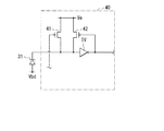
- FIG. 9 is a circuit diagram illustrating a configuration example of a pixel according to a comparative example.
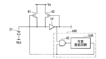
- FIG. 15 is a circuit diagram illustrating a configuration example of a pixel according to another comparative example.
- FIG. 5 is a circuit diagram illustrating a configuration example of a pixel illustrated in FIG. 4.
- FIG. 9 is a circuit diagram illustrating a configuration example of a pixel according to a modification.
- FIG. 11 is an explanatory diagram illustrating an example of a process of adjusting a delay time of a variable delay circuit according to another modification.
- FIG. 11 is an explanatory diagram illustrating an example of a process of adjusting a delay time of a variable delay circuit according to another modification.
- FIG. 13 is a configuration diagram illustrating a configuration example of a time measurement device according to an application example. It is a block diagram showing an example of a schematic structure of a vehicle control system. It is explanatory drawing which shows an example of the installation position of a vehicle exterior information detection part and an imaging part.
- FIG. 1 illustrates a configuration example of a time measurement device (time measurement device 1) according to an embodiment.
- the time measuring device 1 is configured to emit light, detect reflected light reflected by the measurement target, and measure a time difference between a timing at which the light is emitted and a timing at which the reflected light is detected.
- the time measuring device 1 includes a light source 11, a light source driving unit 12, a diffusion lens 13, a condenser mirror 14, and a time measuring device 20.
- the light source 11 is driven by the light source driving unit 12 and is configured to emit light.
- the light source 11 is configured using, for example, a pulse laser light source.
- the light source driving unit 12 is configured to drive the light source 11 based on the light emission trigger signal TRG. Specifically, based on the light emission trigger signal TRG supplied from the time measurement device 20, the light source driving unit 12 causes the light source 11 to emit light at a timing corresponding to a trigger pulse included in the light emission trigger signal TRG. , The operation of the light source 11 is controlled.
- the diffusion lens 13 is configured to diffuse the light emitted from the light source 11 within a predetermined angle range.
- the light (emitted light L1) diffused by the diffusion lens 13 is emitted from the time measuring device 1.
- the focusing mirror 14 is configured to reflect light (reflected light L ⁇ b> 2) reflected by the measurement object 9 and incident on the time measuring device 1 toward the light receiving surface S of the time measuring device 20.
- the time measuring device 20 detects the light reflected by the condenser mirror 14, and determines the time difference between the timing when the light source 11 emits the light and the timing when the light receiving element 31 (described later) of the time measuring device 20 detects the light. It is configured to measure. Since the light incident on the time measuring device 20 is substantially the same as the light reflected on the measurement object 9 and incident on the time measuring device 1, the light incident on the time measuring device 20 will be described below for convenience of description. Is also referred to as reflected light L2.
- the time measurement device 20 also performs an operation of generating a light emission trigger signal TRG and supplying the generated light emission trigger signal TRG to the light source driving unit 12.
- the time measurement device 20 also performs a calibration process for adjusting the delay time of the variable delay circuit 50 included in the pixel 30 as described later.
- FIG. 2 shows an example of the configuration of the time measuring device 20.
- the time measurement device 20 includes a pixel array 21, a selection signal generation unit 22, a signal generation unit 23, a synchronization unit 24, an addition unit 25, a histogram generation unit 26, a processing unit 27, and a control unit 28. Have.
- the pixel array 21 has a plurality of pixels 30 arranged in a matrix.
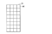
- FIG. 3 shows one configuration example of the pixel array 21.
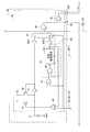
- FIG. 4 illustrates a configuration example of the pixel 30.
- the pixel 30 has a light receiving element 31 and a pixel circuit 40.
- the light receiving element 31 is a photoelectric conversion element that detects light, and is configured using, for example, a single photon avalanche diode (SPAD).
- the voltage Vbd is supplied to the anode of the light receiving element 31, and the cathode is connected to the pixel circuit 40.
- the pixel circuit 40 includes transistors 41 and 42, an inverter IV, a logical sum (OR) circuit 43, a ring oscillator 44, a logical sum circuit 46, and level conversion circuits BUF1 and BUF2. , A selector 47, a logical product (AND) circuit 48, and a logical sum circuit 49.
- the transistors 41 and 42 are P-type MOS (Metal Oxide Semiconductor) transistors.
- the voltage Ve is supplied to the source of the transistor 41, the gate is connected to the output terminal of the OR circuit 46, and the drain is connected to the cathode of the light receiving element 31, the drain of the transistor 42, and the input terminal of the inverter IV.
- the voltage Ve is supplied to the source of the transistor 42, the gate is connected to the output terminal of the inverter IV, the first input terminal of the OR circuit 43, and the input terminal of the level conversion circuit BUF1, and the drain is the cathode of the light receiving element 31.
- the drain of the transistor 41 and the input terminal of the inverter IV are P-type MOS (Metal Oxide Semiconductor) transistors.
- the input terminal of the inverter IV is connected to the cathode of the light receiving element 31 and the drains of the transistors 41 and 42, and the output terminal is connected to the gate of the transistor 42, the first input terminal of the OR circuit 43, and the input terminal of the level conversion circuit BUF1. Connected.
- the first input terminal of the OR circuit 43 is connected to the output terminal of the inverter IV, the gate of the transistor 42, and the input terminal of the level conversion circuit BUF1, and the control signal EN_CAL is supplied to the second input terminal. Is connected to the ring oscillator 44.
- the ring oscillator 44 has an inverted logical product (NAND) circuit 45 and a variable delay circuit 50.
- a first input terminal of the inversion AND circuit 45 is connected to an output terminal of the OR circuit 43, and a second input terminal is an output terminal of the variable delay circuit 50, an input terminal of the level conversion circuit BUF2, and an OR circuit 46. And the output terminal is connected to the input terminal of the variable delay circuit 50.
- the variable delay circuit 50 is configured to delay the signal supplied from the inversion AND circuit 45 by a delay time corresponding to the control signal DSET.
- the input terminal of the variable delay circuit 50 is connected to the output terminal of the inverting AND circuit 45, and the output terminal is the input terminal of the level conversion circuit BUF2, the second input terminal of the inverting AND circuit 45, and the output terminal of the OR circuit 46. 2 input terminals.
- the inversion AND circuit 45 inverts the signal at the second input terminal and outputs the inverted signal. Thereby, the ring oscillator 44 performs an oscillating operation, and generates an oscillating signal SO having a frequency corresponding to the delay time in the variable delay circuit 50.
- the inversion AND circuit 45 outputs a high level.
- the ring oscillator 44 stops the oscillating operation.
- FIG. 5A to 5E show specific examples of the configuration of the ring oscillator 44.
- FIG. These ring oscillators 44 differ from each other in the configuration of the variable delay circuit 50.
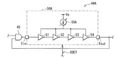
- the ring oscillator 44 (ring oscillator 44A) shown in FIG. 5A has a variable delay circuit 50A.
- the variable delay circuit 50A has four inverters 51 to 54 and a current source 59A.
- Each of the four inverters 51 to 54 is, for example, a CMOS (complementary metal oxide semiconductor) inverter.
- the input terminal of the inverter 51 is connected to the input terminal Tin of the variable delay circuit 50A, and the output terminal is connected to the input terminal of the inverter 52.
- the input terminal of the inverter 52 is connected to the output terminal of the inverter 51, and the output terminal is connected to the input terminal of the inverter 53.
- the input terminal of the inverter 53 is connected to the output terminal of the inverter 52, and the output terminal is connected to the input terminal of the inverter 54.
- the input terminal of the inverter 54 is connected to the output terminal of the inverter 53, and the output terminal is connected to the output terminal Tout of the variable delay circuit 50A.
- Power supply terminals of inverters 51 to 54 are connected to current source 59A.
- the current source 59A is configured to allow a current to flow from one end to the other end and change the current value of the current based on the control signal DSET.
- the voltage Ve is supplied to one end of the current source 59A, and the other end is connected to the power supply terminals of the inverters 51 to 54.
- the delay time in the variable delay circuit 50A changes according to the current value of the current generated by the current source 59A. Specifically, for example, when the current value of the current generated by the current source 59A is large, the delay time in the inverters 51 to 54 is short, and when the current value of the current generated by the current source 59A is small, The delay time in the inverters 51 to 54 becomes longer. In this way, the ring oscillator 44A performs an oscillating operation at a frequency corresponding to the delay time in the variable delay circuit 50A.
- the ring oscillator 44 (ring oscillator 44B) shown in FIG. 5B has a variable delay circuit 50B.
- the variable delay circuit 50B has four inverters 51 to 54 and four current sources 51B, 52B, 53B and 54B.
- Each of the current sources 51B, 52B, 53B, and 54B is configured to allow a current to flow from one end to the other end, and to be able to change the current value of the current based on the control signal DSET.
- the voltage Ve is supplied to one end of the current source 51B, and the other end is connected to the power supply terminal of the inverter 51.
- the voltage Ve is supplied to one end of the current source 52B, and the other end is connected to the power supply terminal of the inverter 52.
- the voltage Ve is supplied to one end of the current source 53B, and the other end is connected to a power supply terminal of the inverter 53.
- the voltage Ve is supplied to one end of the current source 54B, and the other end is connected to a power supply terminal of the inverter 54.
- the delay time in the variable delay circuit 50B changes according to the current value of the current generated by the current sources 51B, 52B, 53B, 54B. Specifically, for example, when the current value of the current generated by the current source 51B is large, the delay time in the inverter 51 is short, and when the current value of the current generated by the current source 51B is small, the inverter 51 , The delay time becomes longer. The same applies to inverters 52 to 54. Thus, the ring oscillator 44B performs an oscillating operation at a frequency corresponding to the delay time in the variable delay circuit 50B.
- the ring oscillator 44 (ring oscillator 44C) shown in FIG. 5C has a variable delay circuit 50C.
- the variable delay circuit 50C has four inverters 51 to 54 and four variable capacitance elements 51C, 52C, 53C, and 54C.
- Each of the four variable capacitance elements 51C, 52C, 53C, 54C is configured to be able to change the capacitance value based on the control signal DSET.
- One end of the variable capacitance element 51C is connected to the output terminal of the inverter 51 and the input terminal of the inverter 52, and the other end is grounded.
- variable capacitance element 52C One end of the variable capacitance element 52C is connected to the output terminal of the inverter 52 and the input terminal of the inverter 53, and the other end is grounded. One end of the variable capacitance element 53C is connected to the output terminal of the inverter 53 and the input terminal of the inverter 54, and the other end is grounded. One end of the variable capacitance element 54C is connected to the output terminal of the inverter 53 and the second input terminal of the AND circuit 45, and the other end is grounded.
- the delay time in the variable delay circuit 50C changes according to the capacitance values of the variable capacitance elements 51C, 52C, 53C, 54C. Specifically, for example, when the capacitance value of the variable capacitance element 51C is small, the delay time in the inverter 51 is short, and when the capacitance value of the variable capacitance element 51C is large, the delay time in the inverter 51 is long. . The same applies to inverters 52 to 54. In this way, the ring oscillator 44C performs an oscillating operation at a frequency corresponding to the delay time in the variable delay circuit 50C.
- the ring oscillator 44 (ring oscillator 44D) shown in FIG. 5D has a variable delay circuit 50D.
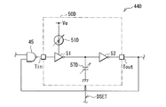
- the variable delay circuit 50D has two inverters 51 and 52, a current source 51D, and a variable capacitance element 57D.
- the output terminal of the inverter 52 is connected to the output terminal Tout of the variable delay circuit 50D.
- the current source 51D is configured to allow a current to flow from one end to the other end and change the current value of the current based on the control signal DSET.
- the voltage Ve is supplied to one end of the current source 51D, and the other end is connected to a power supply terminal of the inverter 51.
- variable capacitance element 57D is configured to be able to change the capacitance value based on the control signal DSET.
- One end of the variable capacitance element 57D is connected to the output terminal of the inverter 51 and the input terminal of the inverter 52, and the other end is grounded.
- the delay time in the variable delay circuit 50D changes according to the current value of the current generated by the current source 51D and the capacitance value of the variable capacitance element 57D. Specifically, for example, when the current value of the current generated by the current source 51D is large and the capacitance value of the variable capacitance element 57D is small, the delay time in the inverter 51 is short. Further, for example, when the current value of the current generated by the current source 51D is small and the capacitance value of the variable capacitance element 57D is large, the delay time in the inverter 51 becomes long. Thus, ring oscillator 44D performs an oscillating operation at a frequency corresponding to the delay time in variable delay circuit 50D.
- the variable range of the delay time in the inverter 51 can be widened. As a result, the number of inverters in the variable delay circuit 50D can be reduced. it can.
- the ring oscillator 44 (ring oscillator 44E) shown in FIG. 5E has a variable delay circuit 50E.
- the variable delay circuit 50E has six inverters 51 to 56 and a selector 58.
- the output terminal of the inverter 52 is connected to the input terminal of the inverter 53 and the first input terminal of the selector 58.
- An output terminal of the inverter 54 is connected to an input terminal of the inverter 55 and a second input terminal of the selector 58.
- the input terminal of the inverter 55 is connected to the output terminal of the inverter 54, and the output terminal is connected to the input terminal of the inverter 56.
- the input terminal of the inverter 56 is connected to the output terminal of the inverter 55, and the output terminal is connected to the third input terminal of the selector 58.
- the selector 58 selects one of a signal at the first input terminal, a signal at the second input terminal, and a signal at the third input terminal based on the control signal DSET, and outputs the selected signal. It is configured to output from the terminal.
- the first input terminal of the selector 58 is connected to the output terminal of the inverter 52 and the input terminal of the inverter 53, the second input terminal is connected to the output terminal of the inverter 54 and the input terminal of the inverter 55, and the third input terminal Is connected to the output terminal of the inverter 56, and the output terminal is connected to the output terminal Tout of the variable delay circuit 50E.
- the delay time in the variable delay circuit 50E changes according to the selection operation in the selector 58.
- the delay time in the variable delay circuit 50E is the sum of the delay time in the two inverters 51 and 52 and the delay time in the selector 58.
- the selector 58 selects the signal at the second input terminal, the total time of the delay times of the four inverters 51 to 54 and the delay time of the selector 58 is satisfied. Is the total time of the delay time in the six inverters 51 to 56 and the delay time in the selector 58. In this way, the ring oscillator 44E performs an oscillating operation at a frequency corresponding to the delay time in the variable delay circuit 50E.
- the variable delay circuit 50 is configured to be able to change the delay time based on the control signal DSET.
- the delay time of the variable delay circuit 50 is adjusted for each area AR.
- Each of the plurality of areas AR includes a plurality of pixels 30.
- One control signal DSET is supplied to the variable delay circuits 50 in the plurality of pixels 30 belonging to one area AR. Thereby, the delay settings in the plurality of variable delay circuits 50 belonging to one area AR become the same.
- the delay time of the variable delay circuit 50 is adjusted in units of the area AR.
- a control signal EN_CAL is supplied to a first input terminal of the OR circuit 46 (FIG. 4), and a second input terminal is an output terminal of the variable delay circuit 50, an input terminal of the level conversion circuit BUF2, and an inversion AND circuit. 45 is connected to the second input terminal, and the output terminal is connected to the gate of the transistor 41.
- the level conversion circuits BUF1 and BUF2 are configured to convert the voltage level of the signal at the input terminal and output the converted signal from the output terminal.
- the input terminal of the level conversion circuit BUF1 is connected to the output terminal of the inverter IV, the gate of the transistor 42, and the first input terminal of the OR circuit 43, and the output terminal is connected to the first input terminal of the selector 47.
- the input terminal of the level conversion circuit BUF2 is connected to the output terminal of the variable delay circuit 50, the second input terminal of the inverting AND circuit 45, and the second input terminal of the OR circuit 46, and the other end is connected to the selector 47. 2 input terminals.
- the selector 47 is configured to select one of the signal at the first input terminal and the signal at the second input terminal based on the control signal EN_CAL, and output the selected signal from the output terminal.
- the first input terminal of the selector 47 is connected to the output terminal of the level conversion circuit BUF1, the second input terminal is connected to the output terminal of the level conversion circuit BUF2, and the output terminal is the first input terminal of the AND circuit 48. Connected to.
- the selector 47 selects the signal at the first input terminal when the control signal EN_CAL is at a low level (L), and selects the signal at the second input terminal when the control signal EN_CAL is at a high level (H). Is selected.
- the first input terminal of the AND circuit 48 is connected to the output terminal of the selector 47, the selection signal SEL is supplied to the second input terminal, and the output terminal is connected to the first input terminal of the OR circuit 49. Is done.
- the first input terminal of the OR circuit 49 is connected to the output terminal of the AND circuit 48, the second input terminal is connected to the input terminal IN of the pixel 30, and the output terminal is connected to the output terminal OUT of the pixel 30.
- the selector 47 outputs a pulse signal SP including the light receiving pulse PL.
- the control signal EN_CAL is at a high level
- the pixel 30 operates in the calibration mode
- the ring oscillator 44 performs an oscillating operation to generate an oscillating signal SO
- the selector 47 outputs the oscillating signal SO. It is supposed to.
- the signal supplied from the signal generation unit 23 is supplied to the input terminal IN of the leftmost pixel 30 of one row of the pixels 30 arranged side by side in the pixel array 21.
- SIN is input.
- the input terminals IN of the pixels 30 other than the leftmost pixel 30 of the one row of pixels 30 are connected to the output terminals OUT of the pixels 30 adjacent to the left side of the pixel 30. It is connected to the.
- the output terminal OUT of the rightmost pixel 30 of the pixels 30 for one row is connected to the synchronization unit 24 as shown in FIG. Then, the rightmost pixel 30 outputs the signal S1.
- one row of the pixels 30 arranged side by side in FIG. 2 is connected in a so-called daisy chain.
- one selection signal SEL is supplied to one column of pixels 30 arranged in the pixel array 21 in the vertical direction, and different selection signals SEL are supplied to the pixels 30 belonging to different columns. .
- the corresponding selection signal SEL is supplied to one row of the pixels 30 arranged side by side in the horizontal direction.
- the selection signal generation unit 22 is configured to generate a plurality of selection signals SEL based on the control signal supplied from the control unit 28.
- the selection signal generation unit 22 supplies the plurality of selection signals SEL to a plurality of columns of the pixels 30 in the pixel array 21. Thereby, the selection signal generation unit 22 can sequentially select the plurality of pixels 30 in units of columns.
- the signal generator 23 is configured to generate the signal SIN including the reference pulse PR based on the control signal supplied from the controller 28.
- the reference pulse PR is generated at a timing corresponding to the timing at which the light source 11 emits light.
- the synchronization unit 24 is configured to generate a plurality of signals S2 by sampling the plurality of signals S1 supplied from the pixel array 21 with the clock signal CK supplied from the control unit 28, respectively.
- the synchronization section 24 has a plurality of flip-flops 64.
- the plurality of flip-flops 64 are provided corresponding to the plurality of rows of the pixels 30 in the pixel array 21.
- Each of the plurality of flip-flops 64 is configured to generate the signal S2 by sampling the signal S1 supplied from the row of the corresponding pixel 30 with the clock signal CK.
- the addition unit 25 is configured to generate a plurality of signals S3 by performing an addition process based on the plurality of signals S2 supplied from the synchronization unit 24 and the control signal supplied from the control unit 28. .
- the adding section 25 has a plurality of adding circuits 65.
- the plurality of adding circuits 65 are provided corresponding to a plurality of rows of the area AR in the pixel array 21. For example, as shown in FIG. 6, when the pixel array 21 has an area AR for eight rows, the adding unit 25 includes eight adding circuits 65.
- Each of the plurality of adding circuits 65 is configured to generate a signal S3 by performing an adding process based on a plurality of signals S2 output from a plurality of flip-flops 64 related to a row of a corresponding area AR. .
- the histogram generator 26 is configured to perform a histogram generation process based on the plurality of signals S3 supplied from the adder 25 and the control signal supplied from the controller 28.
- the histogram generation unit 26 has a plurality of histogram generation circuits 66.
- the plurality of histogram generation circuits 66 are provided corresponding to the plurality of addition circuits 65.
- Each of the plurality of histogram generation circuits 66 is configured to generate a histogram by performing a histogram generation process based on the signal S3 supplied from the corresponding addition circuit 65.
- the processing unit 27 is configured to generate the depth image PIC based on the information on the histogram supplied from the histogram generation unit 26 and the control signal supplied from the control unit 28. Each of the plurality of pixel values included in the depth image PIC indicates a depth value.
- the processing unit 27 outputs the generated depth image PIC.
- the processing unit 27 has a delay time measuring unit 27A.
- the delay time measurement unit 27A performs a variable delay based on the information on the histogram supplied from the histogram generation unit 26 and the control signal supplied from the control unit 28.
- the delay time of the circuit 50 is configured to be measured.
- the delay time measuring section 27A supplies information on the measured delay time to the control section 28.
- the control unit 28 supplies a control signal to the pixel array 21, the selection signal generation unit 22, the signal generation unit 23, the synchronization unit 24, the addition unit 25, the histogram generation unit 26, and the processing unit 27, and a light source driving unit.
- the control unit 28 has a light emission timing setting unit 28A and a delay control unit 28B.
- the light emission timing setting unit 28A is configured to generate a light emission trigger signal TRG for instructing the light emission timing of the light source 11.
- the light emission trigger signal TRG includes a plurality of trigger pulses.
- the control unit 28 supplies the light emission trigger signal TRG to the light source drive unit 12 so that the light source 11 emits light at a timing corresponding to a trigger pulse included in the light emission trigger signal TRG. Control.
- the delay control unit 28B is configured to control the delay time of the variable delay circuit 50 of the pixel 30. Specifically, when operating in the calibration mode, the delay control unit 28B sets the control signal EN_CAL to a high level (active). Then, the delay control unit 28B calculates, based on the information supplied from the delay time measurement unit 27A of the processing unit 27, the delay time of the variable delay circuit 50 of each of the plurality of pixels 30 in the pixel array 21 for each area AR. Determine your settings. Then, the delay control unit 28B generates the control signal DSET based on the determination result. Thereby, in each of the plurality of variable delay circuits 50, the delay time is set so as to be a predetermined length of time.
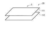
- the time measuring device 20 is formed on, for example, two semiconductor substrates that are overlapped with each other.
- FIG. 7 illustrates a configuration example of the time measurement device 20.
- the time measuring device 20 is configured using two semiconductor substrates 111 and 112 which are superimposed.
- the light receiving element 31 in the pixel array 21 is formed on the semiconductor substrate 111. Therefore, in the time measuring device 20, the surface on which the semiconductor substrate 111 is arranged is the light receiving surface S.
- a pixel circuit 40 in the pixel array 21 is formed in a region corresponding to a region where the light receiving element 31 is formed in the semiconductor substrate 111.
- a selection signal generation unit 22, a signal generation unit 23, a synchronization unit 24, an addition unit 25, a histogram generation unit 26, a processing unit 27, and a control unit 28 are further formed.
- the semiconductor substrate 111 and the semiconductor substrate 112 are overlapped with each other and are electrically connected by, for example, a Cu—Cu junction.
- variable delay circuit 50 corresponds to a specific example of “delay circuit” in the present disclosure.
- the synchronization unit 24, the addition unit 25, the histogram generation unit 26, and the processing unit 27 correspond to a specific example of “time measurement unit” in the present disclosure.
- the transistor 41 corresponds to a specific example of “switch” in the present disclosure.
- the selector 47 corresponds to a specific example of “selector” in the present disclosure.
- the light emission timing setting unit 28A of the control unit 28 generates a light emission trigger signal TRG for instructing the light emission timing of the light source 11.
- the light source driving unit 12 drives the light source 11 based on the light emission trigger signal TRG.
- the light source 11 emits light at a timing corresponding to a trigger pulse included in the light emission trigger signal TRG.
- the diffusion lens 13 diffuses the light emitted from the light source 11 within a predetermined angle range.
- the light (emitted light L1) diffused by the diffusion lens 13 is emitted from the time measuring device 1.
- the converging mirror 14 reflects the light (reflected light L ⁇ b> 2) reflected by the measurement object 9 and incident on the time measuring device 1 toward the light receiving surface S of the time measuring device 20.
- the time measuring device 20 generates the depth image PIC by detecting the light reflected by the condenser mirror 14.
- the selection signal generation unit 22 sequentially selects the plurality of pixels 30 in the pixel array 21 in units of columns by generating the plurality of selection signals SEL based on the control signal supplied from the control unit 28. I do.
- the signal generator 23 generates a signal SIN based on the control signal supplied from the controller 28.
- the plurality of pixels 30 belonging to the selected column in the pixel array 21 each output a pulse signal SP including a light receiving pulse PL corresponding to the reflected light L2.
- the pixel array 21 outputs these pulse signals SP as a plurality of signals S1.
- the synchronization unit 24 generates each of the plurality of signals S2 by sampling each of the plurality of signals S1 with the clock signal CK.
- the adder 25 generates a plurality of signals S3 by performing an addition process based on the plurality of signals S2.
- the histogram generation unit 26 performs a histogram generation process based on the plurality of signals S3.
- the processing unit 27 generates the depth image PIC based on the information on the histogram supplied from the histogram generation unit 26.
- the delay control unit 28B of the control unit 28 sets the control signal EN_CAL to a high level (active).
- the selection signal generation unit 22 sequentially selects a plurality of pixels 30 in the pixel array 21 in units of columns by generating a plurality of selection signals SEL based on the control signal supplied from the control unit 28.
- the ring oscillator 44 performs an oscillating operation.
- each of the plurality of pixels 30 outputs an oscillation signal SO having a frequency corresponding to the delay time in the variable delay circuit 50.
- the pixel array 21 outputs these oscillation signals SO as a plurality of signals S1.
- the synchronization unit 24 generates each of the plurality of signals S2 by sampling each of the plurality of signals S1 with the clock signal CK.
- the adder 25 generates a plurality of signals S3 by performing an addition process based on the plurality of signals S2.
- the histogram generation unit 26 performs a histogram generation process based on the plurality of signals S3.
- the delay time measurement unit 27A of the processing unit 27 measures the delay time of the variable delay circuit 50 based on the information on the histogram supplied from the histogram generation unit 26. Then, the delay time measuring unit 27A supplies information on the measured delay time to the control unit 28.
- the delay control unit 28B of the control unit 28 sets the delay time of the variable delay circuit 50 of each of the plurality of pixels 30 in the pixel array 21 for each area AR based on the information supplied from the delay time measurement unit 27A. decide. Then, the delay control unit 28B generates the control signal DSET based on the determination result. As a result, in each of the plurality of variable delay circuits 50, the delay time is set to be a predetermined length of time.
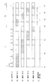
- FIGS. 8A and 8B show an operation example of the time measuring device 1.
- FIG. 8A shows the waveform of the emitted light L1 emitted from the light source 11, and
- FIG. 8B shows the first column of the pixel array 21 from the left.
- C shows the operation of the pixel 30 (2) in the second column from the left in the pixel array 21, and
- D shows the operation of the pixel 30 (2) in the third column from the left in the pixel array 21.
- E) shows the operation,
- E) shows the operation of the pixel 30 (N) in the rightmost column (Nth column) in the pixel array 21, and
- (F) shows the waveform of the control signal EN_CAL. 8B to 8E, the shaded portion indicates that the pixel 30 is selected, and the unshaded portion indicates that the pixel 30 is not selected.
- the time measuring device 1 generates a depth image by emitting light and detecting light reflected by the measurement object 9 during the measurement period T1.
- the time measurement device 1 performs a calibration process for adjusting the delay time of the variable delay circuit 50 included in the pixel 30 in a period (a blanking period T2) between two measurement periods T1 adjacent to each other.
- a blanking period T2 a period between two measurement periods T1 adjacent to each other.
- the delay control unit 28B sets the control signal EN_CAL to low level (FIG. 8F). Then, during a period from timing t1 to timing t2, the selection signal generation unit 22 selects the pixel 30 (1) in the first column (FIG. 8B).
- the light emission timing setting unit 28A generates a light emission trigger signal TRG.
- the light source driving unit 12 controls the light source 11 based on the light emission trigger signal TRG so that the light source 11 emits the light pulse a plurality of times in a predetermined light emission cycle (light emission cycle T) during the period from the timing t1 to the time t2.
- the operation is controlled (FIG. 8A).
- the pixel 30 (1) outputs a pulse signal SP including the light receiving pulse PL corresponding to the incident reflected light L2.
- the pixel array 21 outputs the pulse signal SP as a signal S1.
- the synchronizing unit 24 generates each of the plurality of signals S2 by sampling each of the plurality of signals S1 with the clock signal CK during the period from the timing t1 to the timing t2.
- the adder 25 generates a plurality of signals S3 by performing an addition process based on the plurality of signals S2.
- the histogram generation unit 26 performs a histogram generation process based on the plurality of signals S3. In this manner, a histogram related to the pixel 30 (1) in the first column is generated.
- the selection signal generation unit 22 selects the pixel 30 (2) in the second column (FIG. 8C). Then, based on the light emission trigger signal TRG, the light source driving unit 12 controls the operation of the light source 11 so that the light source 11 emits the light pulse a plurality of times in the light emission cycle T during the period from the timing t2 to the timing t3 ( FIG. 8 (A)). As a result, the pixel 30 (2) outputs a pulse signal SP including the light receiving pulse PL corresponding to the incident reflected light L2. The pixel array 21 outputs the pulse signal SP as a signal S1.
- the synchronization unit 24 generates the plurality of signals S2 by sampling the plurality of signals S1 with the clock signal CK during the period from the timing t2 to the timing t3.
- the adder 25 generates a plurality of signals S3 by performing an addition process based on the plurality of signals S2.
- the histogram generation unit 26 performs a histogram generation process based on the plurality of signals S3. In this way, a histogram related to the pixel 30 (2) in the second column is generated.
- the time measuring device 1 sequentially selects the plurality of pixels 30 in the pixel array 21 in column units during the period from the timing t1 to the timing t4 (measurement period T1). As a result, a histogram relating to the pixels 30 in each column is generated.
- the processing unit 27 generates a depth image based on the histogram generated in the period of the timings t1 to t4 (measurement period T1).
- the delay control unit 28B of the control unit 28 sets the control signal EN_CAL to a high level (active) (FIG. 8F). Then, during the period from timing t4 to t5, the selection signal generation unit 22 selects the pixel 30 (1) in the first column (FIG. 8B). Accordingly, the ring oscillator 44 of the pixel 30 (1) performs an oscillating operation, and the pixel 30 (1) outputs an oscillating signal SO having a frequency corresponding to the delay time in the variable delay circuit 50. The pixel array 21 outputs the oscillation signal SO as a signal S1.
- the synchronizing unit 24 generates the plurality of signals S2 by sampling the plurality of signals S1 with the clock signal CK during the period from the timing t4 to the timing t5.
- the adder 25 generates a plurality of signals S3 by performing an addition process based on the plurality of signals S2.
- the histogram generation unit 26 performs a histogram generation process based on the plurality of signals S3. In this manner, a histogram related to the pixel 30 (1) in the first column is generated.
- the delay control unit 28B sets the control signal EN_CAL to a low level (inactive) (FIG. 8F).
- the selection signal generation unit 22 selects the pixel 30 (2) in the second column (FIG. 8C). Accordingly, the ring oscillator 44 of the pixel 30 (2) performs an oscillating operation, and the pixel 30 (2) outputs an oscillating signal SO having a frequency corresponding to the delay time in the variable delay circuit 50.
- the pixel array 21 outputs the oscillation signal SO as a signal S1.
- the synchronization unit 24 generates the plurality of signals S2 by sampling the plurality of signals S1 with the clock signal CK during the period from the timing t5 to the timing t6.
- the adder 25 generates a plurality of signals S3 by performing an addition process based on the plurality of signals S2.
- the histogram generation unit 26 performs a histogram generation process based on the plurality of signals S3. In this way, a histogram related to the pixel 30 (2) in the second column is generated.
- the delay control unit 28B sets the control signal EN_CAL to a low level (inactive) (FIG. 8F).
- the time measuring device 1 sequentially selects the plurality of pixels 30 in the pixel array 21 in column units during the period from the timing t4 to the timing t7 (the blanking period T2). As a result, a histogram relating to the pixels 30 in each column is generated.
- the delay time measuring unit 27A of the processing unit 27 measures the delay time of the variable delay circuit 50 based on the information on the histogram supplied from the histogram generating unit 26.
- the delay control unit 28B of the control unit 28 sets the delay time of the variable delay circuit 50 of each of the plurality of pixels 30 in the pixel array 21 for each area AR based on the information supplied from the delay time measurement unit 27A. decide. Then, the delay control unit 28B generates the control signal DSET based on the determination result.
- the delay time is set to be a predetermined length of time.
- the calibration process is performed in the blanking period T2, but the calibration process may not be performed in all blanking periods T2.
- the calibration process can be performed once in a predetermined number of blanking periods T2.
- FIG. 9 schematically illustrates the operation of the selected pixel 30 during the measurement period T1. Since the control signal EN_CAL is at a low level during the measurement period T1, the selector 47 outputs a signal at the first input terminal. When the light receiving element 31 detects the reflected light L2, the voltage of the cathode of the light receiving element 31 becomes low during a predetermined length of time. In response, the output voltage of inverter IV goes high during a period of a predetermined length. Thus, the light receiving pulse PL is generated in the pixel 30. Then, the pulse signal SP including the light receiving pulse PL is output via the level conversion circuit BUF1, the selector 47, the AND circuit 48, and the OR circuit 49.
- FIG. 10A and 10B show the operation of the selected pixel 30 during the measurement period T1, where FIG. 10A shows the waveform of the voltage (cathode voltage) at the cathode of the light receiving element 31, and FIG. 10B shows the output of the inverter IV.
- C shows the waveform of the output voltage of the OR circuit 43
- D shows the waveform of the output voltage of the variable delay circuit 50
- E shows the waveform of the output voltage of the OR circuit 46. The waveform is shown.
- the cathode voltage of the light receiving element 31 decreases from the voltage Ve (FIG. 10A).
- the inverter IV changes the output voltage from a low level to a high level at a timing t12 (FIG. 10B).
- the transistor 42 is turned off.
- the OR circuit 43 changes the output voltage from a low level to a high level at a timing t13 (FIG. 10C). That is, in the measurement period T1, the control signal EN_CAL is at the low level, and the OR circuit 43 changes the output voltage from the low level to the high level according to the change in the output voltage of the inverter IV.
- the inverting AND circuit 45 changes the output voltage from a high level to a low level.
- the delay circuit 50 changes the output voltage from the high level to the low level (FIG. 10D). That is, at the timing t13, since the output voltage of the variable delay circuit 50 is at the high level, the inversion AND circuit 45 changes the output voltage from the high level to the low level in accordance with the change of the output voltage of the OR circuit 43. Let it. Then, the variable delay circuit 50 changes the output voltage from the high level to the low level at a timing delayed by the delay time corresponding to the control signal DSET in accordance with the change in the output voltage of the inversion AND circuit 45. .
- the time between the timing t13 and the timing t14 is the total time (delay time td) of the delay time of the inverting AND circuit 45 and the delay time of the variable delay circuit 50. Since the delay time of the variable delay circuit 50 is sufficiently longer than the delay time of the inversion AND circuit 45, the delay time td is substantially equal to the delay time of the variable delay circuit 50.
- the OR circuit 46 changes the output voltage from a high level to a low level at a timing t15 (FIG. 10E). That is, in the measurement period T1, the control signal EN_CAL is at the low level, and the OR circuit 46 changes the output voltage from the high level to the low level according to the change in the output voltage of the variable delay circuit 50.
- the transistor 41 In response to the change in the output voltage of the OR circuit 46, the transistor 41 is turned on, and at the timing t16, the cathode voltage of the light receiving element 31 increases and becomes the voltage Ve (FIG. 10A). In response to the change in the cathode voltage, the inverter IV changes the output voltage from a high level to a low level at a timing t17 (FIG. 10B). Thus, the transistor 42 is turned on.
- the OR circuit 43 changes the output voltage from a high level to a low level at a timing t18 (FIG. 10C).
- the inversion AND circuit 45 changes the output voltage from a low level to a high level, and in response to the change in the output voltage of the inversion AND circuit 45.
- the variable delay circuit 50 changes the output voltage from a low level to a high level at a timing t19 (FIG. 10D).
- the OR circuit 46 changes the output voltage from a low level to a high level at a timing t20 (FIG. 10E).
- the transistor 41 is turned off.
- the pulse width of the light receiving pulse PL is controlled by the delay time td.
- the pulse width of the light receiving pulse PL is controlled by the delay time of the variable delay circuit 50.
- FIGS. 11A and 11B show an operation example of the time measuring device 20 in the measuring period T1, (A) shows the waveform of the signal SIN, (B) shows the waveform of the signal S1, and (C) shows the signal S2. (D) shows the waveform of the signal S3.
- the waveform is illustrated using the clock cycle TCK.
- the signal generator 23 changes the voltage of the signal SIN from a low level to a high level, and at timing t22, changes the voltage of the signal SIN from a high level to a low level (FIG. 11A).
- the reference pulse PR is generated at a timing corresponding to the timing at which the light source 11 emits light. This reference pulse PR is transmitted via one row of pixels 30 in the pixel array 21 in a daisy chain connection.
- the pixel array 21 changes the voltage of the signal S1 from the low level to the high level, and at the timing t24, changes the voltage of the signal S1 from the high level to the low level (FIG. 11B). . In this way, the pixel array 21 outputs the reference pulse PR supplied from the signal generator 23.
- the pixel array 21 changes the voltage of the signal S1 from a low level to a high level, and at a timing t26, the voltage of the signal S1 is changed. Is changed from a high level to a low level (FIG. 11B).
- the pixel array 21 outputs the first light receiving pulse PL (light receiving pulse PL1).
- the pixel array 21 changes the voltage of the signal S1 from a low level to a high level at a subsequent timing t27.
- the voltage of S1 is changed from a high level to a low level (FIG. 11B).
- the pixel array 21 outputs the second light receiving pulse PL (light receiving pulse PL2).
- the flip-flop 64 of the synchronization unit 24 generates the signal S2 by sampling the signal S1 with the clock signal CK (FIG. 11C).
- the addition circuit 65 of the addition unit 25 generates a signal S3 by performing an addition process based on the plurality of signals S2 output from the plurality of flip-flops 64 (FIG. 11D).
- the histogram generation circuit 66 of the histogram generation unit 26 generates a histogram by performing a histogram generation process based on the signal S3.
- the processing unit 27 measures a time difference ⁇ t between the timing when the light source 11 emits light and the timing when the light receiving element 31 of the time measuring device 20 detects light. Specifically, the processing unit 27 measures the time difference ⁇ t1 based on the histogram related to the reference pulse PR and the histogram related to the received light pulse PL1, and calculates the time difference ⁇ t2 based on the histogram related to the reference pulse PR and the histogram related to the received light pulse PL2. Is measured. For example, the processing unit 27 may measure the time difference ⁇ t using the peak timing in the histogram, or may measure the time difference ⁇ t using the edge timing in the histogram.
- the processing unit 27 generates the depth image PIC based on the time difference ⁇ t.
- FIG. 12 schematically illustrates the operation of the selected pixel 30 in the calibration mode.
- the selector 47 outputs a signal at the second input terminal.
- the OR circuit 43 outputs a high level, so that the ring oscillator 44 performs an oscillating operation.
- ring oscillator 44 generates oscillation signal SO having a frequency corresponding to the delay time in variable delay circuit 50.
- This oscillation signal SO is output via the level conversion circuit BUF2, the selector 47, the AND circuit 48, and the OR circuit 49.
- the operation of the time measuring device 20 in the calibration mode will be described by taking an example of the operation of a selected pixel 30 among the pixels 30 of one selected column.
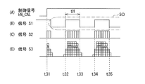
- FIGS. 13A and 13B show an operation example of the time measuring device 20 in the calibration mode.
- FIG. 13A shows the waveform of the control signal EN_CAL
- FIG. 13B shows the waveform of the signal S1
- FIG. The waveform of S2 is shown
- (D) shows the waveform of signal S3.
- the waveform is illustrated using the clock cycle TCK.
- the delay control unit 28B of the control unit 28 changes the voltage of the control signal EN_CAL from a low level to a high level (FIG. 13A).
- the ring oscillator 44 performs an oscillating operation, and generates an oscillating signal SO having a frequency corresponding to the delay time in the variable delay circuit 50.
- the pixel array 21 outputs the oscillation signal SO as the signal S1 (FIG. 13B).
- the flip-flop 64 of the synchronization unit 24 generates the signal S2 by sampling the signal S1 with the clock signal CK (FIG. 13C).
- the addition circuit 65 of the addition unit 25 generates a signal S3 by performing an addition process based on the plurality of signals S2 output from the plurality of flip-flops 64 (FIG. 13D).
- the histogram generation circuit 66 of the histogram generation unit 26 generates a histogram by performing a histogram generation process based on the signal S3.
- the delay time measuring unit 27A of the processing unit 27 measures the delay time of the variable delay circuit 50 based on the signal S3. Specifically, the delay time measuring unit 27A measures the time length tH of the period when the oscillation signal SO is at a high level. The delay time measuring unit 27A can measure the time length tH using, for example, edge timings at both ends in the histogram. This time length tH corresponds to the total time (delay time td shown in FIG. 10) of the delay time of the inverting AND circuit 45 and the delay time of the variable delay circuit 50 in the ring oscillator 44.
- the delay time measuring section 27A measures the delay time of the variable delay circuit 50.
- the delay time measuring unit 27A supplies information on the measured delay time to the control unit 28.
- the delay control unit 28B of the control unit 28 sets the delay time of the variable delay circuit 50 of each of the plurality of pixels 30 in the pixel array 21 for each area AR based on the information supplied from the delay time measurement unit 27A. decide. Then, the delay control unit 28B generates the control signal DSET based on the determination result. As a result, in each of the plurality of variable delay circuits 50, the delay time is set to be a predetermined length of time.
- the transistor 41 is provided in each pixel 30, and the light receiving element 31 receives the reflected light L2, so that the cathode voltage of the light receiving element 31 decreases and a predetermined time elapses.
- the transistor 41 is turned on.
- the dead time can be reduced as compared with a configuration in which the light receiving element 31 and the resistance element 41R are connected in series without providing the transistor 41.
- a variable delay circuit 50 is provided for each pixel 30, and a pulse signal SP including a light receiving pulse PL having a pulse width corresponding to the delay time of the variable delay circuit 50 is generated.
- the time measurement device 20 measures the delay time of the variable delay circuit 50, and based on the measurement result, sets the delay time of the variable delay circuit 50 to a predetermined length of time. Set to.
- the dead time can be shortened. That is, for example, as shown in FIG. 15, when the ring oscillator 44R is configured by using the delay circuit 50R instead of the variable delay circuit 50, the delay circuit 50R Will change. In this case, since the length of the dead time also changes, the dead time may be long.
- the delay time of the variable delay circuit 50 is set to be a predetermined length of time, the change in the length of the dead time can be suppressed, and the dead time can be reduced. can do.
- the ring oscillator 44 is configured using the variable delay circuit 50 in the calibration mode, and the delay time of the variable delay circuit 50 is measured based on the oscillation signal SO of the ring oscillator 44. did.
- the delay time of the variable delay circuit 50 can be measured based on the time corresponding to a half cycle of the oscillation signal SO, so that the delay time of the variable delay circuit 50 can be measured by a simple method.
- the time measurement device 20 performs the calibration process using the synchronization unit 24, the addition unit 25, and the histogram generation unit 26 used in the time measurement process.
- the number of circuits to be added for performing the calibration process can be reduced, so that the circuit configuration can be simplified.
- the transistor 41 is provided in each pixel, and the transistor is turned on at a timing when a predetermined time has elapsed after the cathode voltage of the light receiving element has decreased due to the light receiving element receiving the reflected light. Since the on state is set, the dead time can be shortened.
- a variable delay circuit is provided for each pixel, and a pulse signal including a light receiving pulse having a pulse width corresponding to the delay time of the variable delay circuit is generated. Then, in the calibration mode, the delay time of the variable delay circuit is measured, and based on the measurement result, the delay time of the variable delay circuit is set to a predetermined length of time. Thereby, the dead time can be shortened.
- the ring oscillator in the calibration mode, is configured using the variable delay circuit, and the delay time of the variable delay circuit is measured based on the oscillation signal of the ring oscillator.
- the delay time of the variable delay circuit can be measured.
- the circuit configuration can be simplified.
- the cathode of the light receiving element 31 is connected to the pixel circuit 40, but the invention is not limited to this.
- the anode of the light receiving element may be connected to the pixel circuit.
- the pixel according to the present modification has a light receiving element 31A and a pixel circuit 40A.
- the anode of the light receiving element 31A is connected to the pixel circuit 40A, and the voltage V1 is supplied to the cathode.
- the pixel circuit 40A has transistors 41A and 42A and an inverter IV.
- the transistors 41A and 41B are N-type MOS transistors.
- the drain of the transistor 41A is connected to the anode of the light receiving element 31A, the drain of the transistor 42A, and the input terminal of the inverter IV, and the source is supplied with the voltage V2.
- the drain of the transistor 42A is connected to the anode of the light receiving element 31A, the drain of the transistor 41A, and the input terminal of the inverter IV, the gate is connected to the output terminal of the inverter IV, and the source is supplied with the voltage V2.
- the present technology is applied to the time measuring device having the configuration illustrated in FIG. 1, but is not limited thereto.
- the time measuring device may be applied to a time measuring device having a configuration shown in FIG.
- the time measuring device 2 includes a lens 71, a pixel array 72, a lens 73, a pixel array 74, and a time measuring unit 75.
- the lens 71 is configured to diffuse the light emitted from the light source 11 within a predetermined angle range.
- the lens 71 reflects a part of the light emitted from the light source 11 toward the pixel array 72.
- the pixel array 72 is configured to detect light reflected by the lens 71 as reference light.
- the pixel array 72 has, for example, the same configuration as the pixel array 21 according to the above embodiment.
- the lens 73 is configured to form an image on the light receiving surface S of the pixel array 74.
- the light reflected by the measurement object 9 (reflected light L2) enters the lens 73.
- the pixel array 74 is configured to detect the reflected light L2. This pixel array 74 has the same configuration as the pixel array 21 according to the above embodiment.
- the time measurement unit 75 generates the depth image PIC by measuring the time difference between the timing of emitting light and the timing of detecting reflected light based on the signal S1 supplied from the pixel arrays 72 and 74. It is composed of
- the technology (the present technology) according to the present disclosure can be applied to various products.
- the technology according to the present disclosure is realized as a device mounted on any type of moving object such as an automobile, an electric vehicle, a hybrid electric vehicle, a motorcycle, a bicycle, a personal mobility, an airplane, a drone, a ship, and a robot. You may.
- FIG. 21 is a block diagram illustrating a schematic configuration example of a vehicle control system that is an example of a mobile object control system to which the technology according to the present disclosure can be applied.
- Vehicle control system 12000 includes a plurality of electronic control units connected via communication network 12001.
- the vehicle control system 12000 includes a drive system control unit 12010, a body system control unit 12020, an outside information detection unit 12030, an inside information detection unit 12040, and an integrated control unit 12050.
- a microcomputer 12051, an audio / video output unit 12052, and a vehicle-mounted network I / F (interface) 12053 are illustrated.
- the drive system control unit 12010 controls the operation of the device related to the drive system of the vehicle according to various programs.
- the drive system control unit 12010 includes a drive force generation device for generating a drive force of the vehicle such as an internal combustion engine or a drive motor, a drive force transmission mechanism for transmitting the drive force to the wheels, and a steering angle of the vehicle. It functions as a control mechanism such as a steering mechanism for adjusting and a braking device for generating a braking force of the vehicle.
- the body control unit 12020 controls the operation of various devices mounted on the vehicle body according to various programs.
- the body-related control unit 12020 functions as a keyless entry system, a smart key system, a power window device, or a control device for various lamps such as a head lamp, a back lamp, a brake lamp, a blinker, and a fog lamp.
- a radio wave or a signal of various switches transmitted from a portable device replacing the key can be input to the body control unit 12020.
- the body control unit 12020 receives the input of these radio waves or signals and controls a door lock device, a power window device, a lamp, and the like of the vehicle.
- Out-of-vehicle information detection unit 12030 detects information external to the vehicle on which vehicle control system 12000 is mounted.
- an imaging unit 12031 is connected to the outside-of-vehicle information detection unit 12030.
- the out-of-vehicle information detection unit 12030 causes the imaging unit 12031 to capture an image outside the vehicle, and receives the captured image.
- the out-of-vehicle information detection unit 12030 may perform an object detection process or a distance detection process on a person, a vehicle, an obstacle, a sign, or a character on a road surface based on the received image.
- the imaging unit 12031 is an optical sensor that receives light and outputs an electric signal according to the amount of received light.
- the imaging unit 12031 can output an electric signal as an image or can output the information as distance measurement information.
- the light received by the imaging unit 12031 may be visible light or non-visible light such as infrared light.
- the in-vehicle information detection unit 12040 detects information in the vehicle.
- the in-vehicle information detection unit 12040 is connected to, for example, a driver status detection unit 12041 that detects the status of the driver.
- the driver state detection unit 12041 includes, for example, a camera that captures an image of the driver, and the in-vehicle information detection unit 12040 determines the degree of driver fatigue or concentration based on the detection information input from the driver state detection unit 12041. The calculation may be performed, or it may be determined whether the driver has fallen asleep.
- the microcomputer 12051 calculates a control target value of the driving force generation device, the steering mechanism or the braking device based on the information on the inside and outside of the vehicle acquired by the outside information detection unit 12030 or the inside information detection unit 12040, and the drive system control unit A control command can be output to 12010.
- the microcomputer 12051 implements the functions of ADAS (Advanced Driver Assistance System) including vehicle collision avoidance or impact mitigation, following running based on the following distance, vehicle speed maintaining running, vehicle collision warning, or vehicle lane departure warning. Cooperative control for the purpose.
- ADAS Advanced Driver Assistance System
- the microcomputer 12051 controls the driving force generation device, the steering mechanism, the braking device, and the like based on the information about the surroundings of the vehicle obtained by the outside information detection unit 12030 or the inside information detection unit 12040, so that the driver 120 It is possible to perform cooperative control for automatic driving or the like in which the vehicle travels autonomously without depending on the operation.
- the microcomputer 12051 can output a control command to the body system control unit 12020 based on information on the outside of the vehicle acquired by the outside information detection unit 12030.
- the microcomputer 12051 controls the headlamp according to the position of the preceding vehicle or the oncoming vehicle detected by the outside information detection unit 12030, and performs cooperative control for the purpose of preventing glare such as switching a high beam to a low beam. It can be carried out.
- the sound image output unit 12052 transmits at least one of a sound signal and an image signal to an output device capable of visually or audibly notifying a passenger of the vehicle or the outside of the vehicle of information.
- an audio speaker 12061, a display unit 12062, and an instrument panel 12063 are illustrated as output devices.
- the display unit 12062 may include, for example, at least one of an on-board display and a head-up display.
- FIG. 22 is a diagram illustrating an example of an installation position of the imaging unit 12031.
- the vehicle 12100 includes imaging units 12101, 12102, 12103, 12104, and 12105 as the imaging unit 12031.
- the imaging units 12101, 12102, 12103, 12104, and 12105 are provided, for example, at positions such as a front nose, a side mirror, a rear bumper, a back door, and an upper part of a windshield in the vehicle interior of the vehicle 12100.
- the imaging unit 12101 provided in the front nose and the imaging unit 12105 provided in the upper part of the windshield in the passenger compartment mainly acquire an image in front of the vehicle 12100.
- the imaging units 12102 and 12103 provided in the side mirror mainly acquire images of the side of the vehicle 12100.
- the imaging unit 12104 provided in the rear bumper or the back door mainly acquires an image behind the vehicle 12100.
- the forward images acquired by the imaging units 12101 and 12105 are mainly used for detecting a preceding vehicle, a pedestrian, an obstacle, a traffic light, a traffic sign, a lane, and the like.
- FIG. 22 shows an example of the imaging range of the imaging units 12101 to 12104.
- the imaging range 12111 indicates the imaging range of the imaging unit 12101 provided on the front nose
- the imaging ranges 12112 and 12113 indicate the imaging ranges of the imaging units 12102 and 12103 provided on the side mirrors, respectively
- the imaging range 12114 indicates 13 shows an imaging range of an imaging unit 12104 provided in a rear bumper or a back door. For example, by overlaying image data captured by the imaging units 12101 to 12104, an overhead image of the vehicle 12100 viewed from above can be obtained.
- At least one of the imaging units 12101 to 12104 may have a function of acquiring distance information.
- at least one of the imaging units 12101 to 12104 may be a stereo camera including a plurality of imaging elements or an imaging element having pixels for detecting a phase difference.
- the microcomputer 12051 calculates a distance to each three-dimensional object in the imaging ranges 12111 to 12114 and a temporal change in the distance (relative speed with respect to the vehicle 12100). , It is possible to extract, as a preceding vehicle, a three-dimensional object that travels at a predetermined speed (for example, 0 km / h or more) in the substantially same direction as the vehicle 12100, which is the closest three-dimensional object on the traveling path of the vehicle 12100. it can.
- a predetermined speed for example, 0 km / h or more
- microcomputer 12051 can set an inter-vehicle distance to be secured before the preceding vehicle and perform automatic brake control (including follow-up stop control), automatic acceleration control (including follow-up start control), and the like. In this way, it is possible to perform cooperative control for automatic driving or the like in which the vehicle travels autonomously without depending on the operation of the driver.
- the microcomputer 12051 converts the three-dimensional object data related to the three-dimensional object into other three-dimensional objects such as a two-wheeled vehicle, a normal vehicle, a large vehicle, a pedestrian, and a telephone pole based on the distance information obtained from the imaging units 12101 to 12104. It can be classified and extracted and used for automatic avoidance of obstacles. For example, the microcomputer 12051 distinguishes obstacles around the vehicle 12100 into obstacles that are visible to the driver of the vehicle 12100 and obstacles that are difficult to see. Then, the microcomputer 12051 determines a collision risk indicating a risk of collision with each obstacle, and when the collision risk is equal to or more than the set value and there is a possibility of collision, via the audio speaker 12061 or the display unit 12062. By outputting a warning to the driver through forced driving and avoidance steering via the drive system control unit 12010, driving assistance for collision avoidance can be performed.
- the microcomputer 12051 converts the three-dimensional object data related to the three-dimensional object into other three-dimensional objects such as a
- At least one of the imaging units 12101 to 12104 may be an infrared camera that detects infrared light.
- the microcomputer 12051 can recognize a pedestrian by determining whether or not a pedestrian exists in the captured images of the imaging units 12101 to 12104. The recognition of such a pedestrian is performed by, for example, extracting a feature point in an image captured by the imaging units 12101 to 12104 as an infrared camera, and performing a pattern matching process on a series of feature points indicating the outline of the object to determine whether the object is a pedestrian.
- the audio image output unit 12052 outputs a rectangular outline to the recognized pedestrian for emphasis.
- the display unit 12062 is controlled so that is superimposed. Further, the sound image output unit 12052 may control the display unit 12062 so as to display an icon or the like indicating a pedestrian at a desired position.
- the technology according to the present disclosure can be applied to the imaging unit 12031 among the configurations described above.
- the dead time is shortened, so that the measurement accuracy can be improved.
- the vehicle control system 12000 it is possible to enhance the accuracy of the vehicle collision avoidance or collision mitigation function, the following traveling function based on the following distance, the vehicle speed maintaining traveling function, the vehicle collision warning function, the vehicle lane departure warning function, and the like. it can.
- the pixel 30 is not limited to the configuration illustrated in FIG. 4, and may use various configurations in which the pulse width of the light receiving pulse PL can be set using the variable delay circuit 50.
- the present technology can be configured as follows.
- (1) It has a light receiving element and a delay circuit capable of changing a delay time, and can output a pulse signal including a light receiving pulse having a pulse width corresponding to the delay time as an output signal in the first operation mode.
- a ring oscillator can be configured by using the delay circuit, and a pixel that can output an oscillation signal in the ring oscillator as the output signal;
- a time measuring unit capable of performing a time measuring process based on the output signal.
- the oscillation signal transitions between a first logic level and a second logic level;
- the time measurement device according to (2) wherein the time measurement process includes measuring a delay time of the delay circuit by measuring a length of time during which the first logic level is continued.
- the time measurement device according to (2) or (3) further including a delay control unit that can adjust the delay time of the delay circuit based on the delay time measured by the time measurement unit.
- a plurality of the pixels The delay time of the delay circuit in the plurality of pixels is set based on one delay setting,
- the time measurement process includes measuring the delay time of the delay circuit in the plurality of pixels based on the plurality of oscillation signals output from the plurality of pixels in the second operation mode.
- the time measurement device according to (4), wherein the delay control unit can generate the delay setting based on the delay time measured by the time measurement unit.
- the time measurement process includes detecting a light receiving timing of the light receiving element based on the pulse signal in the first operation mode. Time measurement device.
- the pixel has a switch capable of connecting the light receiving node and the first power supply node when the pixel is turned on; The light receiving element is inserted between the light receiving node and a second power supply node, The delay circuit delays a signal according to a voltage of the light receiving node in the first operation mode,
- the time measurement device according to any one of (1) to (6), wherein the switch can be turned on based on a signal delayed by the delay circuit in the first operation mode.
- the pixel further has a selector,
- the pulse signal is a signal according to the voltage of the light receiving node,
- the selector according to (7), wherein the selector can select the pulse signal as the output signal in the first operation mode, and can select the oscillation signal as the output signal in the second operation mode.
- Time measurement device (9)
- the light receiving element is formed on a first semiconductor substrate,
- the time measurement device according to (7) or (8), wherein the delay circuit and the switch are formed on a second semiconductor substrate superimposed on the first semiconductor substrate.
- the time measuring device according to any one of (1) to (9), wherein the light receiving element is a single photon avalanche diode.
- a light source capable of emitting light
- a pulse including a light receiving element capable of detecting reflected light corresponding to the light and a delay circuit capable of changing a delay time, the light receiving pulse having a pulse width corresponding to the delay time in the first operation mode
- a pixel that can output a signal as an output signal, and in the second operation mode, can configure a ring oscillator using the delay circuit, and can output an oscillation signal in the ring oscillator as the output signal;
- a time measurement unit capable of performing a time measurement process based on the output signal.
Landscapes
- Engineering & Computer Science (AREA)
- Physics & Mathematics (AREA)
- Computer Networks & Wireless Communication (AREA)
- General Physics & Mathematics (AREA)
- Radar, Positioning & Navigation (AREA)
- Remote Sensing (AREA)
- Electromagnetism (AREA)
- Optical Radar Systems And Details Thereof (AREA)
- Measurement Of Unknown Time Intervals (AREA)
Abstract
本開示の時間計測デバイスは、受光素子と、遅延時間を変更可能な遅延回路とを有し、第1の動作モードにおいて、遅延時間に応じたパルス幅を有する受光パルスを含むパルス信号を出力信号として出力可能であり、第2の動作モードにおいて、遅延回路を用いてリングオシレータを構成可能であり、リングオシレータにおける発振信号を出力信号として出力可能な画素と、出力信号に基づいて時間計測処理を行うことが可能な時間計測部とを備える。
Description
本開示は、光を射出したタイミングから光を検出したタイミングまでの時間を計測する時間計測デバイスおよび時間計測装置に関する。
計測対象物までの距離を測定する際、しばしば、TOF(Time Of Flight)法が用いられる。このTOF法では、光を射出するとともに、計測対象物により反射された反射光を検出する。そして、TOF法では、光を射出したタイミングおよび反射光を検出したタイミングの間の時間差を計測することにより、計測対象物までの距離を計測する。
ところで、受光素子には、しばしばアバランシェフォトダイオードが用いられる。特許文献1には、アバランシェフォトダイオードおよび抵抗素子が直列接続された光受信装置が開示されている。
このような受光素子を含む回路では、フォトンを検出した後に、しばらくの間、次のフォトンを検出しにくい期間がある。この期間の長さは、デッドタイムとも呼ばれる。時間計測デバイスでは、このデッドタイムが短いことが望まれる。
デッドタイムを短くすることができる時間計測デバイスおよび時間計測装置を提供することが望ましい。
本開示の一実施の形態における時間計測デバイスは、画素と、時間計測部とを備える。画素は、受光素子と、遅延時間を変更可能な遅延回路とを有し、第1の動作モードにおいて、遅延時間に応じたパルス幅を有する受光パルスを含むパルス信号を出力信号として出力可能であり、第2の動作モードにおいて、遅延回路を用いてリングオシレータを構成可能であり、リングオシレータにおける発振信号を出力信号として出力可能に構成される。時間計測部は、出力信号に基づいて時間計測処理を行うことが可能に構成される。
本開示の一実施の形態における時間計測装置は、光源と、画素と、時間計測部とを備える。光源は、光を射出可能に構成される。画素は、光に対応する反射光を検出可能な受光素子と、遅延時間を変更可能な遅延回路とを有し、第1の動作モードにおいて、遅延時間に応じたパルス幅を有する受光パルスを含むパルス信号を出力信号として出力可能であり、第2の動作モードにおいて、遅延回路を用いてリングオシレータを構成可能であり、リングオシレータにおける発振信号を出力信号として出力可能に構成される。時間計測部は、出力信号に基づいて時間計測処理を行うことが可能に構成される。
本開示の一実施の形態における時間計測デバイスおよび時間計測装置では、受光素子と、遅延時間を変更可能な遅延回路とを用いて、画素が構成される。第1の動作モードでは、遅延時間に応じたパルス幅を有する受光パルスを含むパルス信号が、画素から出力される。第2の動作モードでは、遅延回路を用いてリングオシレータが構成され、このリングオシレータにおける発振信号が、画素から出力される。そして、この画素から出力された信号に基づいて、時間計測処理が行われる。
本開示の一実施の形態における時間計測デバイスおよび時間計測装置によれば、第2の動作モードにおいて、画素が発振信号を出力し、時間計測部がこの信号に基づいて時間計測処理を行うようにしたので、デッドタイムを短くすることができる。なお、ここに記載された効果は必ずしも限定されるものではなく、本開示中に記載されたいずれの効果があってもよい。
以下、本開示の実施の形態について、図面を参照して詳細に説明する。なお、説明は以下の順序で行う。
1.実施の形態
2.適用例
3.移動体への応用例
1.実施の形態
2.適用例
3.移動体への応用例
<1.実施の形態>
[構成例]
図1は、一実施の形態に係る時間計測装置(時間計測装置1)の一構成例を表すものである。時間計測装置1は、光を射出するとともに、計測対象物により反射された反射光を検出し、光を射出したタイミングおよび反射光を検出したタイミングの間の時間差を計測するように構成される。時間計測装置1は、光源11と、光源駆動部12と、拡散レンズ13と、集光ミラー14と、時間計測デバイス20とを備えている。
[構成例]
図1は、一実施の形態に係る時間計測装置(時間計測装置1)の一構成例を表すものである。時間計測装置1は、光を射出するとともに、計測対象物により反射された反射光を検出し、光を射出したタイミングおよび反射光を検出したタイミングの間の時間差を計測するように構成される。時間計測装置1は、光源11と、光源駆動部12と、拡散レンズ13と、集光ミラー14と、時間計測デバイス20とを備えている。
光源11は、光源駆動部12により駆動され、光を射出するように構成される。光源11は、例えば、パルスレーザ光源を用いて構成される。
光源駆動部12は、発光トリガ信号TRGに基づいて光源11を駆動するように構成される。具体的には、光源駆動部12は、時間計測デバイス20から供給された発光トリガ信号TRGに基づいて、光源11が発光トリガ信号TRGに含まれるトリガパルスに応じたタイミングで光を射出するように、光源11の動作を制御するようになっている。
拡散レンズ13は、光源11から射出した光を所定の角度範囲内に拡散させるように構成される。そして、拡散レンズ13により拡散された光(出射光L1)は、時間計測装置1から射出されるようになっている。
集光ミラー14は、計測対象物9により反射されて時間計測装置1に入射した光(反射光L2)を、時間計測デバイス20の受光面Sに向けて反射させるように構成される。
時間計測デバイス20は、集光ミラー14により反射された光を検出し、光源11が光を射出したタイミングおよび時間計測デバイス20の受光素子31(後述)が光を検出したタイミングの間の時間差を計測するように構成される。時間計測デバイス20に入射する光は、計測対象物9により反射されて時間計測装置1に入射した光と実質的に同じであるので、以下では、説明の便宜上、時間計測デバイス20に入射する光を反射光L2とも呼ぶ。また、時間計測デバイス20は、発光トリガ信号TRGを生成し、生成した発光トリガ信号TRGを光源駆動部12に供給する動作をも行うようになっている。
また、時間計測デバイス20は、キャリブレーションモードにおいて、後述するように、画素30に含まれる可変遅延回路50の遅延時間を調整するキャリブレーション処理をも行うようになっている。
図2は、時間計測デバイス20の一構成例を表すものである。時間計測デバイス20は、画素アレイ21と、選択信号生成部22と、信号生成部23と、同期部24と、加算部25と、ヒストグラム生成部26と、処理部27と、制御部28とを備えている。
画素アレイ21は、マトリクス状に配置された複数の画素30を有している。
図3は、画素アレイ21の一構成例を表すものである。この図3は、画素アレイ21における複数の画素30のうちの4個(=2×2)の画素30を図示している。図4は、画素30の一構成例を表すものである。画素30は、受光素子31と、画素回路40とを有している。
受光素子31は、光を検出する光電変換素子であり、例えば、シングルフォトンアバランシェダイオード(SPAD)を用いて構成される。受光素子31のアノードには電圧Vbdが供給され、カソードは画素回路40に接続されている。
画素回路40は、図4に示したように、トランジスタ41,42と、インバータIVと、論理和(OR)回路43と、リングオシレータ44と、論理和回路46と、レベル変換回路BUF1,BUF2と、セレクタ47と、論理積(AND)回路48と、論理和回路49とを有している。
トランジスタ41,42は、P型のMOS(Metal Oxide Semiconductor)トランジスタである。トランジスタ41のソースには電圧Veが供給され、ゲートは論理和回路46の出力端子に接続され、ドレインは受光素子31のカソード、トランジスタ42のドレイン、およびインバータIVの入力端子に接続される。トランジスタ42のソースには電圧Veが供給され、ゲートはインバータIVの出力端子、論理和回路43の第1の入力端子、およびレベル変換回路BUF1の入力端子に接続され、ドレインは受光素子31のカソード、トランジスタ41のドレイン、およびインバータIVの入力端子に接続される。
インバータIVの入力端子は受光素子31のカソードおよびトランジスタ41,42のドレインに接続され、出力端子はトランジスタ42のゲート、論理和回路43の第1の入力端子、およびレベル変換回路BUF1の入力端子に接続される。
論理和回路43の第1の入力端子はインバータIVの出力端子、トランジスタ42のゲート、およびレベル変換回路BUF1の入力端子に接続され、第2の入力端子には制御信号EN_CALが供給され、出力端子はリングオシレータ44に接続される。
リングオシレータ44は、反転論理積(NAND)回路45と、可変遅延回路50とを有している。反転論理積回路45の第1の入力端子は論理和回路43の出力端子に接続され、第2の入力端子は可変遅延回路50の出力端子、レベル変換回路BUF2の入力端子、および論理和回路46の第2の入力端子に接続され、出力端子は可変遅延回路50の入力端子に接続される。可変遅延回路50は、反転論理積回路45から供給された信号を、制御信号DSETに応じた遅延時間の分だけ遅延するように構成される。可変遅延回路50の入力端子は反転論理積回路45の出力端子に接続され、出力端子はレベル変換回路BUF2の入力端子、反転論理積回路45の第2の入力端子、および論理和回路46の第2の入力端子に接続される。
リングオシレータ44では、反転論理積回路45は、第1の入力端子での信号が高レベルである場合には、第2の入力端子での信号を反転し、反転された信号を出力する。これにより、リングオシレータ44は、発振動作を行い、可変遅延回路50における遅延時間に応じた周波数を有する発振信号SOを生成する。また、反転論理積回路45は、第1の入力端子での信号が低レベルである場合には、高レベルを出力する。これにより、リングオシレータ44は、発振動作を停止するようになっている。
図5A~5Eは、リングオシレータ44の具体的な構成例を表すものである。これらのリングオシレータ44は、可変遅延回路50の構成が互いに異なっている。
図5Aに示したリングオシレータ44(リングオシレータ44A)は、可変遅延回路50Aを有している。可変遅延回路50Aは、4つのインバータ51~54と、電流源59Aとを有している。4つのインバータ51~54のそれぞれは、例えば、CMOS(complementary metal oxide semiconductor)インバータである。インバータ51の入力端子は可変遅延回路50Aの入力端子Tinに接続され、出力端子はインバータ52の入力端子に接続される。インバータ52の入力端子はインバータ51の出力端子に接続され、出力端子はインバータ53の入力端子に接続される。インバータ53の入力端子はインバータ52の出力端子に接続され、出力端子はインバータ54の入力端子に接続される。インバータ54の入力端子はインバータ53の出力端子に接続され、出力端子は可変遅延回路50Aの出力端子Toutに接続される。インバータ51~54の電源端子は電流源59Aに接続される。電流源59Aは、一端から他端に向かって電流を流すとともに、制御信号DSETに基づいて、その電流の電流値を変更可能に構成される。電流源59Aの一端には電圧Veが供給され、他端はインバータ51~54の電源端子に接続される。
リングオシレータ44Aでは、可変遅延回路50Aにおける遅延時間が、電流源59Aが生成する電流の電流値に応じて変化する。具体的には、例えば、電流源59Aが生成する電流の電流値が大きい場合には、インバータ51~54における遅延時間が短くなり、電流源59Aが生成する電流の電流値が小さい場合には、インバータ51~54における遅延時間が長くなる。このようにして、リングオシレータ44Aは、可変遅延回路50Aにおける遅延時間に応じた周波数で発振動作を行うようになっている。
図5Bに示したリングオシレータ44(リングオシレータ44B)は、可変遅延回路50Bを有している。可変遅延回路50Bは、4つのインバータ51~54と、4つの電流源51B,52B,53B,54Bとを有している。電流源51B,52B,53B,54Bのそれぞれは、一端から他端に向かって電流を流すとともに、制御信号DSETに基づいて、その電流の電流値を変更可能に構成される。電流源51Bの一端には電圧Veが供給され、他端はインバータ51の電源端子に接続される。電流源52Bの一端には電圧Veが供給され、他端はインバータ52の電源端子に接続される。電流源53Bの一端には電圧Veが供給され、他端はインバータ53の電源端子に接続される。電流源54Bの一端には電圧Veが供給され、他端はインバータ54の電源端子に接続される。
リングオシレータ44Bでは、可変遅延回路50Bにおける遅延時間が、電流源51B,52B,53B,54Bが生成する電流の電流値に応じて変化する。具体的には、例えば、電流源51Bが生成する電流の電流値が大きい場合には、インバータ51における遅延時間が短くなり、電流源51Bが生成する電流の電流値が小さい場合には、インバータ51における遅延時間が長くなる。インバータ52~54についても同様である。これにより、リングオシレータ44Bは、可変遅延回路50Bにおける遅延時間に応じた周波数で発振動作を行うようになっている。
図5Cに示したリングオシレータ44(リングオシレータ44C)は、可変遅延回路50Cを有している。可変遅延回路50Cは、4つのインバータ51~54と、4つの可変容量素子51C,52C,53C,54Cとを有している。4つの可変容量素子51C,52C,53C,54Cのそれぞれは、制御信号DSETに基づいて容量値を変更可能に構成される。可変容量素子51Cの一端はインバータ51の出力端子およびインバータ52の入力端子に接続され、他端は接地される。可変容量素子52Cの一端はインバータ52の出力端子およびインバータ53の入力端子に接続され、他端は接地される。可変容量素子53Cの一端はインバータ53の出力端子およびインバータ54の入力端子に接続され、他端は接地される。可変容量素子54Cの一端はインバータ53の出力端子および反転論理積回路45の第2の入力端子に接続され、他端は接地される。
リングオシレータ44Cでは、可変遅延回路50Cにおける遅延時間が、可変容量素子51C,52C,53C,54Cの容量値に応じて変化する。具体的には、例えば、可変容量素子51Cの容量値が小さい場合には、インバータ51における遅延時間が短くなり、可変容量素子51Cの容量値が大きい場合には、インバータ51における遅延時間が長くなる。インバータ52~54についても同様である。このようにして、リングオシレータ44Cは、可変遅延回路50Cにおける遅延時間に応じた周波数で発振動作を行うようになっている。
図5Dに示したリングオシレータ44(リングオシレータ44D)は、可変遅延回路50Dを有している。可変遅延回路50Dは、2つのインバータ51,52と、電流源51Dと、可変容量素子57Dとを有している。インバータ52の出力端子は、可変遅延回路50Dの出力端子Toutに接続される。電流源51Dは、一端から他端に向かって電流を流すとともに、制御信号DSETに基づいて、その電流の電流値を変更可能に構成される。電流源51Dの一端には電圧Veが供給され、他端はインバータ51の電源端子に接続される。可変容量素子57Dは、制御信号DSETに基づいて容量値を変更可能に構成される。可変容量素子57Dの一端はインバータ51の出力端子およびインバータ52の入力端子に接続され、他端は接地される。
リングオシレータ44Dでは、可変遅延回路50Dにおける遅延時間が、電流源51Dが生成する電流の電流値、および可変容量素子57Dの容量値に応じて変化する。具体的には、例えば、電流源51Dが生成する電流の電流値が大きく、可変容量素子57Dの容量値が小さい場合には、インバータ51における遅延時間が短くなる。また、例えば、電流源51Dが生成する電流の電流値が小さく、可変容量素子57Dの容量値が大きい場合には、インバータ51における遅延時間が長くなる。このようにして、リングオシレータ44Dは、可変遅延回路50Dにおける遅延時間に応じた周波数で発振動作を行う。リングオシレータ44Dでは、電流源51Dおよび可変容量素子57Dを設けるようにしたので、インバータ51における遅延時間の可変範囲を広くすることができ、その結果、可変遅延回路50Dにおけるインバータの数を減らすことができる。
図5Eに示したリングオシレータ44(リングオシレータ44E)は、可変遅延回路50Eを有している。可変遅延回路50Eは、6つのインバータ51~56と、セレクタ58とを有している。インバータ52の出力端子は、インバータ53の入力端子およびセレクタ58の第1の入力端子に接続される。インバータ54の出力端子は、インバータ55の入力端子およびセレクタ58の第2の入力端子に接続される。インバータ55の入力端子はインバータ54の出力端子に接続され、出力端子はインバータ56の入力端子に接続される。インバータ56の入力端子はインバータ55の出力端子に接続され、出力端子はセレクタ58の第3の入力端子に接続される。セレクタ58は、制御信号DSETに基づいて、第1の入力端子における信号、第2の入力端子における信号、および第3の入力端子における信号のうちの1つを選択し、選択された信号を出力端子から出力するように構成される。セレクタ58の第1の入力端子はインバータ52の出力端子およびインバータ53の入力端子に接続され、第2の入力端子はインバータ54の出力端子およびインバータ55の入力端子に接続され、第3の入力端子はインバータ56の出力端子に接続され、出力端子は可変遅延回路50Eの出力端子Toutに接続される。
リングオシレータ44Eでは、可変遅延回路50Eにおける遅延時間が、セレクタ58における選択動作に応じて変化する。具体的には、例えば、可変遅延回路50Eにおける遅延時間は、セレクタ58が第1の入力端子における信号を選択した場合には、2つのインバータ51,52における遅延時間およびセレクタ58における遅延時間の合計時間になり、セレクタ58が第2の入力端子における信号を選択した場合には、4つのインバータ51~54における遅延時間およびセレクタ58における遅延時間の合計時間になり、セレクタ58が第3の入力端子における信号を選択した場合には、6つのインバータ51~56における遅延時間およびセレクタ58における遅延時間の合計時間になる。このようにして、リングオシレータ44Eは、可変遅延回路50Eにおける遅延時間に応じた周波数で発振動作を行うようになっている。
このように、リングオシレータ44では、可変遅延回路50は、制御信号DSETに基づいて、遅延時間を変更可能に構成される。図6に示したように、画素アレイ21では、可変遅延回路50の遅延時間は、エリアAR単位で調整される。この例では、画素アレイ21は、32個(=4×8)のエリアARに区分される。複数のエリアARのそれぞれは、複数の画素30を含む。1つのエリアARに属する複数の画素30における可変遅延回路50には、1つの制御信号DSETが供給される。これにより、1つのエリアARに属する複数の可変遅延回路50における遅延設定は互いに同じになる。このようにして、可変遅延回路50の遅延時間は、エリアAR単位で調整されるようになっている。
論理和回路46(図4)の第1の入力端子には制御信号EN_CALが供給され、第2の入力端子は可変遅延回路50の出力端子、レベル変換回路BUF2の入力端子、および反転論理積回路45の第2の入力端子に接続され、出力端子はトランジスタ41のゲートに接続される。
レベル変換回路BUF1,BUF2は、入力端子における信号の電圧レベルを変換し、変換された信号を出力端子から出力するように構成される。レベル変換回路BUF1の入力端子はインバータIVの出力端子、トランジスタ42のゲート、および論理和回路43の第1の入力端子に接続され、出力端子はセレクタ47の第1の入力端子に接続される。レベル変換回路BUF2の入力端子は可変遅延回路50の出力端子、反転論理積回路45の第2の入力端子、および論理和回路46の第2の入力端子に接続され、他端はセレクタ47の第2の入力端子に接続される。
セレクタ47は、制御信号EN_CALに基づいて、第1の入力端子における信号および第2の入力端子における信号のうちの一方を選択し、選択された信号を出力端子から出力するように構成される。セレクタ47の第1の入力端子はレベル変換回路BUF1の出力端子に接続され、第2の入力端子はレベル変換回路BUF2の出力端子に接続され、出力端子は論理積回路48の第1の入力端子に接続される。セレクタ47は、制御信号EN_CALが低レベル(L)である場合には、第1の入力端子における信号を選択し、制御信号EN_CALが高レベル(H)である場合には、第2の入力端子における信号を選択するようになっている。
論理積回路48の第1の入力端子は、セレクタ47の出力端子に接続され、第2の入力端子には選択信号SELが供給され、出力端子は論理和回路49の第1の入力端子に接続される。
論理和回路49の第1の入力端子は論理積回路48の出力端子に接続され、第2の入力端子は画素30の入力端子INに接続され、出力端子は画素30の出力端子OUTに接続される。
この構成により、画素30では、制御信号EN_CALが低レベルである場合には、受光素子31が反射光L2を受光する度に、可変遅延回路50の遅延時間に応じたパルス幅を有する受光パルスPLを生成し、セレクタ47がこの受光パルスPLを含むパルス信号SPを出力する。また、制御信号EN_CALが高レベルである場合には、画素30はキャリブレーションモードで動作し、リングオシレータ44が発振動作を行うことにより発振信号SOを生成し、セレクタ47がこの発振信号SOを出力するようになっている。
図2に示したように、画素アレイ21において横方向に並設された1行分の画素30のうちの一番左側の画素30の入力端子INには、信号生成部23から供給された信号SINが入力される。また、この1行分の画素30のうちの一番左側の画素30以外の画素30の入力端子INは、図3に示したように、その画素30の左側に隣り合う画素30の出力端子OUTに接続されている。そして、この1行分の画素30のうちの一番右側の画素30の出力端子OUTは、図2に示したように、同期部24に接続されている。そして、この一番右側の画素30は、信号S1を出力する。このように、画素アレイ21では、図2における横方向に並設された1行分の画素30が、いわゆるデイジーチェーン接続されるようになっている。
また、画素アレイ21において縦方向に並設された1列分の画素30には、1つの選択信号SELが供給され、互いに異なる列に属する画素30には、互いに異なる選択信号SELが供給される。言い換えれば、横方向に並設された1行分の画素30には、対応する選択信号SELがそれぞれ供給される。この構成により、画素アレイ21では、複数の画素30が、選択信号SELを用いて、1列分の画素30を単位として選択されるようになっている。
選択信号生成部22は、制御部28から供給された制御信号に基づいて、複数の選択信号SELを生成するように構成される。選択信号生成部22は、これらの複数の選択信号SELを、画素アレイ21における画素30の複数の列にそれぞれに供給する。これにより、選択信号生成部22は、複数の画素30を、列単位で順次選択することができるようになっている。
信号生成部23は、制御部28から供給された制御信号に基づいて、リファレンスパルスPRを含む信号SINを生成するように構成される。このリファレンスパルスPRは、光源11が発光するタイミングに応じたタイミングで生成されるようになっている。
同期部24は、画素アレイ21から供給された複数の信号S1を、制御部28から供給されたクロック信号CKでそれぞれサンプリングすることにより、複数の信号S2をそれぞれ生成するように構成される。同期部24は、複数のフリップフロップ64を有している。複数のフリップフロップ64は、画素アレイ21における画素30の複数の行に対応して設けられている。複数のフリップフロップ64のそれぞれは、対応する画素30の行から供給された信号S1をクロック信号CKでサンプリングすることにより信号S2を生成するように構成される。
加算部25は、同期部24から供給された複数の信号S2、および制御部28から供給された制御信号に基づいて、加算処理を行うことにより、複数の信号S3を生成するように構成される。加算部25は、複数の加算回路65を有している。複数の加算回路65は、画素アレイ21における、エリアARの複数の行に対応して設けられている。例えば、図6に示したように、画素アレイ21が、8行分のエリアARを有する場合には、加算部25は、8個の加算回路65を有している。複数の加算回路65のそれぞれは、対応するエリアARの行に係る複数のフリップフロップ64から出力された複数の信号S2に基づいて加算処理を行うことにより、信号S3を生成するように構成される。
ヒストグラム生成部26は、加算部25から供給された複数の信号S3、および制御部28から供給された制御信号に基づいて、ヒストグラム生成処理を行うように構成される。ヒストグラム生成部26は、複数のヒストグラム生成回路66を有している。複数のヒストグラム生成回路66は、複数の加算回路65に対応して設けられている。複数のヒストグラム生成回路66のそれぞれは、対応する加算回路65から供給された信号S3に基づいてヒストグラム生成処理を行うことにより、ヒストグラムを生成するように構成される。
処理部27は、ヒストグラム生成部26から供給されたヒストグラムについての情報、および制御部28から供給された制御信号に基づいて、デプス画像PICを生成するように構成される。デプス画像PICに含まれる複数の画素値のそれぞれはデプス値を示す。処理部27は、生成したデプス画像PICを出力するようになっている。
処理部27は、遅延時間計測部27Aを有している。遅延時間計測部27Aは、時間計測デバイス20がキャリブレーションモードで動作する場合に、ヒストグラム生成部26から供給されたヒストグラムについての情報、および制御部28から供給された制御信号に基づいて、可変遅延回路50の遅延時間を計測するように構成される。そして、遅延時間計測部27Aは、計測した遅延時間に関する情報を制御部28に供給するようになっている。
制御部28は、画素アレイ21、選択信号生成部22、信号生成部23、同期部24、加算部25、ヒストグラム生成部26、および処理部27に対して制御信号を供給するとともに、光源駆動部12に対して発光トリガ信号TRGを供給することにより、時間計測装置1の動作を制御するように構成される。制御部28は、発光タイミング設定部28Aと、遅延制御部28Bとを有している。
発光タイミング設定部28Aは、光源11における発光タイミングを指示する発光トリガ信号TRGを生成するように構成される。発光トリガ信号TRGは、複数のトリガパルスを含んでいる。制御部28は、この発光トリガ信号TRGを光源駆動部12に供給することにより、光源11が、この発光トリガ信号TRGに含まれるトリガパルスに応じたタイミングで発光するように、光源11の動作を制御するようになっている。
遅延制御部28Bは、画素30の可変遅延回路50の遅延時間を制御するように構成される。具体的には、遅延制御部28Bは、キャリブレーションモードで動作する際、制御信号EN_CALを高レベル(アクティブ)に設定する。そして、遅延制御部28Bは、処理部27の遅延時間計測部27Aから供給された情報に基づいて、エリアAR単位で、画素アレイ21における複数の画素30のそれぞれの可変遅延回路50の遅延時間の設定を決定する。そして、遅延制御部28Bは、決定結果に基づいて、制御信号DSETを生成する。これにより、複数の可変遅延回路50のそれぞれでは、遅延時間が所定の長さの時間になるように設定されるようになっている。
時間計測デバイス20は、例えば、互いに重ね合わされた2枚の半導体基板に形成される。
図7は、時間計測デバイス20の一構成例を表すものである。時間計測デバイス20は、この例では、重ね合わされた2枚の半導体基板111,112を用いて構成される。この半導体基板111には、画素アレイ21における受光素子31が形成される。よって、時間計測デバイス20において、半導体基板111が配置された面が受光面Sである。半導体基板112のうち、半導体基板111において受光素子31が形成された領域に対応する領域には、画素アレイ21における画素回路40が形成される。また、この半導体基板112には、さらに、選択信号生成部22、信号生成部23、同期部24、加算部25、ヒストグラム生成部26、処理部27、および制御部28が形成されている。これらの半導体基板111および半導体基板112は、互いに重ね合わされ、例えばCu-Cu接合により電気的に接続されるようになっている。
ここで、可変遅延回路50は、本開示における「遅延回路」の一具体例に対応する。同期部24、加算部25、ヒストグラム生成部26、および処理部27は、本開示における「時間計測部」の一具体例に対応する。トランジスタ41は、本開示における「スイッチ」の一具体例に対応する。セレクタ47は、本開示における「セレクタ」の一具体例に対応する。
[動作および作用]
続いて、本実施の形態の時間計測装置1の動作および作用について説明する。
続いて、本実施の形態の時間計測装置1の動作および作用について説明する。
(全体動作概要)
まず、図1,2を参照して、時間計測装置1の全体動作概要を説明する。制御部28の発光タイミング設定部28Aは、光源11における発光タイミングを指示する発光トリガ信号TRGを生成する。光源駆動部12は、発光トリガ信号TRGに基づいて光源11を駆動する。光源11は、発光トリガ信号TRGに含まれるトリガパルスに応じたタイミングで光を射出する。拡散レンズ13は、光源11から射出した光を所定の角度範囲内に拡散させる。拡散レンズ13により拡散された光(出射光L1)は、時間計測装置1から射出される。集光ミラー14は、計測対象物9により反射されて時間計測装置1に入射した光(反射光L2)を、時間計測デバイス20の受光面Sに向けて反射させる。
まず、図1,2を参照して、時間計測装置1の全体動作概要を説明する。制御部28の発光タイミング設定部28Aは、光源11における発光タイミングを指示する発光トリガ信号TRGを生成する。光源駆動部12は、発光トリガ信号TRGに基づいて光源11を駆動する。光源11は、発光トリガ信号TRGに含まれるトリガパルスに応じたタイミングで光を射出する。拡散レンズ13は、光源11から射出した光を所定の角度範囲内に拡散させる。拡散レンズ13により拡散された光(出射光L1)は、時間計測装置1から射出される。集光ミラー14は、計測対象物9により反射されて時間計測装置1に入射した光(反射光L2)を、時間計測デバイス20の受光面Sに向けて反射させる。
時間計測デバイス20は、集光ミラー14により反射された光を検出することによりデプス画像PICを生成する。具体的には、選択信号生成部22は、制御部28から供給された制御信号に基づいて、複数の選択信号SELを生成することにより、画素アレイ21における複数の画素30を列単位で順次選択する。信号生成部23は、制御部28から供給された制御信号に基づいて信号SINを生成する。画素アレイ21における選択された列に属する複数の画素30は、反射光L2に応じた受光パルスPLを含むパルス信号SPをそれぞれ出力する。これにより、画素アレイ21は、これらのパルス信号SPを複数の信号S1として出力する。同期部24は、複数の信号S1をクロック信号CKでそれぞれサンプリングすることにより、複数の信号S2をそれぞれ生成する。加算部25は、複数の信号S2に基づいて加算処理を行うことにより、複数の信号S3を生成する。ヒストグラム生成部26は、複数の信号S3に基づいてヒストグラム生成処理を行う。処理部27は、ヒストグラム生成部26から供給されたヒストグラムについての情報に基づいて、デプス画像PICを生成する。
時間計測デバイス20がキャリブレーションモードで動作する場合には、制御部28の遅延制御部28Bは、制御信号EN_CALを高レベル(アクティブ)に設定する。選択信号生成部22は、制御部28から供給された制御信号に基づいて、複数の選択信号SELを生成することにより、画素アレイ21における複数の画素30を列単位で順次選択する。画素アレイ21における選択された列に属する複数の画素30では、リングオシレータ44が発振動作を行う。これにより、これらの複数の画素30は、可変遅延回路50における遅延時間に応じた周波数を有する発振信号SOをそれぞれ出力する。これにより、画素アレイ21は、これらの発振信号SOを複数の信号S1として出力する。同期部24は、複数の信号S1をクロック信号CKでそれぞれサンプリングすることにより、複数の信号S2をそれぞれ生成する。加算部25は、複数の信号S2に基づいて加算処理を行うことにより、複数の信号S3を生成する。ヒストグラム生成部26は、複数の信号S3に基づいてヒストグラム生成処理を行う。処理部27の遅延時間計測部27Aは、ヒストグラム生成部26から供給されたヒストグラムについての情報に基づいて、可変遅延回路50の遅延時間を計測する。そして、遅延時間計測部27Aは、計測した遅延時間に関する情報を制御部28に供給する。制御部28の遅延制御部28Bは、遅延時間計測部27Aから供給された情報に基づいて、エリアAR単位で、画素アレイ21における複数の画素30のそれぞれの可変遅延回路50の遅延時間の設定を決定する。そして、遅延制御部28Bは、決定結果に基づいて、制御信号DSETを生成する。これにより、複数の可変遅延回路50のそれぞれでは、遅延時間が所定の長さの時間になるように設定される。
(詳細動作)
図8は、時間計測装置1の一動作例を表すものであり、(A)は光源11から射出された出射光L1の波形を示し、(B)は画素アレイ21における左から1列目の画素30(1)の動作を示し、(C)は画素アレイ21における左から2列目の画素30(2)の動作を示し、(D)は画素アレイ21における左から3列目の画素30(3)の動作を示し、(E)は画素アレイ21における一番右の列(N列目)の画素30(N)の動作を示し、(F)は制御信号EN_CALの波形を示す。図8(B)~(E)において、網掛けされた部分は、画素30が選択されていることを示し、網掛けされていない部分は、画素30が選択されていないことを示す。
図8は、時間計測装置1の一動作例を表すものであり、(A)は光源11から射出された出射光L1の波形を示し、(B)は画素アレイ21における左から1列目の画素30(1)の動作を示し、(C)は画素アレイ21における左から2列目の画素30(2)の動作を示し、(D)は画素アレイ21における左から3列目の画素30(3)の動作を示し、(E)は画素アレイ21における一番右の列(N列目)の画素30(N)の動作を示し、(F)は制御信号EN_CALの波形を示す。図8(B)~(E)において、網掛けされた部分は、画素30が選択されていることを示し、網掛けされていない部分は、画素30が選択されていないことを示す。
時間計測装置1は、計測期間T1において、光を射出するとともに、計測対象物9により反射された反射光を検出することにより、デプス画像を生成する。また、時間計測装置1は、互いに隣り合う2つの計測期間T1の間の期間(ブランキング期間T2)において、画素30に含まれる可変遅延回路50の遅延時間を調整するキャリブレーション処理を行う。以下に、この動作について詳細に説明する。
タイミングt1において計測期間T1が開始すると、まず、遅延制御部28Bは、制御信号EN_CALを低レベルにする(図8(F))。そして、タイミングt1~t2の期間において、選択信号生成部22は、1列目の画素30(1)を選択する(図8(B))。また、発光タイミング設定部28Aは、発光トリガ信号TRGを生成する。光源駆動部12は、この発光トリガ信号TRGに基づいて、このタイミングt1~t2の期間において、光源11が光パルスを所定の発光周期(発光周期T)で複数回出射するように、光源11の動作を制御する(図8(A))。これにより、画素30(1)は、入射された反射光L2に応じた受光パルスPLを含むパルス信号SPを出力する。画素アレイ21は、このパルス信号SPを信号S1として出力する。
同期部24は、このタイミングt1~t2の期間において、複数の信号S1をクロック信号CKでそれぞれサンプリングすることにより、複数の信号S2をそれぞれ生成する。加算部25は、複数の信号S2に基づいて加算処理を行うことにより、複数の信号S3を生成する。ヒストグラム生成部26は、複数の信号S3に基づいてヒストグラム生成処理を行う。このようにして、1列目の画素30(1)に係るヒストグラムが生成される。
次に、タイミングt2~t3の期間において、選択信号生成部22は、2列目の画素30(2)を選択する(図8(C))。そして、光源駆動部12は、発光トリガ信号TRGに基づいて、このタイミングt2~t3の期間において、光源11が光パルスを発光周期Tで複数回出射するように、光源11の動作を制御する(図8(A))。これにより、画素30(2)は、入射された反射光L2に応じた受光パルスPLを含むパルス信号SPを出力する。画素アレイ21は、このパルス信号SPを信号S1として出力する。
同期部24は、このタイミングt2~t3の期間において、複数の信号S1をクロック信号CKでそれぞれサンプリングすることにより、複数の信号S2をそれぞれ生成する。加算部25は、複数の信号S2に基づいて加算処理を行うことにより、複数の信号S3を生成する。ヒストグラム生成部26は、複数の信号S3に基づいてヒストグラム生成処理を行う。このようにして、2列目の画素30(2)に係るヒストグラムが生成される。
このようにして、時間計測装置1は、タイミングt1~t4の期間(計測期間T1)において、画素アレイ21における複数の画素30を列単位で順次選択する。これにより、各列の画素30に係るヒストグラムがそれぞれ生成される。
そして、処理部27は、このタイミングt1~t4の期間(計測期間T1)において生成されたヒストグラムに基づいて、デプス画像を生成する。
タイミングt4においてブランキング期間T2が開始すると、制御部28の遅延制御部28Bは、制御信号EN_CALを高レベル(アクティブ)に設定する(図8(F))。そして、タイミングt4~t5の期間において、選択信号生成部22は、1列目の画素30(1)を選択する(図8(B))。これにより、画素30(1)のリングオシレータ44は、発振動作を行い、画素30(1)は、可変遅延回路50における遅延時間に応じた周波数を有する発振信号SOを出力する。画素アレイ21は、この発振信号SOを信号S1として出力する。
同期部24は、このタイミングt4~t5の期間において、複数の信号S1をクロック信号CKでそれぞれサンプリングすることにより、複数の信号S2をそれぞれ生成する。加算部25は、複数の信号S2に基づいて加算処理を行うことにより、複数の信号S3を生成する。ヒストグラム生成部26は、複数の信号S3に基づいてヒストグラム生成処理を行う。このようにして、1列目の画素30(1)に係るヒストグラムが生成される。
そして、タイミングt5より前のタイミングにおいて、遅延制御部28Bは、制御信号EN_CALを低レベル(非アクティブ)に設定する(図8(F))。
次に、タイミングt5~t6の期間において、選択信号生成部22は、2列目の画素30(2)を選択する(図8(C))。これにより、画素30(2)のリングオシレータ44は、発振動作を行い、画素30(2)は、可変遅延回路50における遅延時間に応じた周波数を有する発振信号SOを出力する。画素アレイ21は、この発振信号SOを信号S1として出力する。
同期部24は、このタイミングt5~t6の期間において、複数の信号S1をクロック信号CKでそれぞれサンプリングすることにより、複数の信号S2をそれぞれ生成する。加算部25は、複数の信号S2に基づいて加算処理を行うことにより、複数の信号S3を生成する。ヒストグラム生成部26は、複数の信号S3に基づいてヒストグラム生成処理を行う。このようにして、2列目の画素30(2)に係るヒストグラムが生成される。
そして、タイミングt6より前のタイミングにおいて、遅延制御部28Bは、制御信号EN_CALを低レベル(非アクティブ)に設定する(図8(F))。
このようにして、時間計測装置1は、タイミングt4~t7の期間(ブランキング期間T2)において、画素アレイ21における複数の画素30を列単位で順次選択する。これにより、各列の画素30に係るヒストグラムがそれぞれ生成される。
そして、処理部27の遅延時間計測部27Aは、ヒストグラム生成部26から供給されたヒストグラムについての情報に基づいて、可変遅延回路50の遅延時間を計測する。制御部28の遅延制御部28Bは、遅延時間計測部27Aから供給された情報に基づいて、エリアAR単位で、画素アレイ21における複数の画素30のそれぞれの可変遅延回路50の遅延時間の設定を決定する。そして、遅延制御部28Bは、決定結果に基づいて、制御信号DSETを生成する。これにより、複数の可変遅延回路50のそれぞれでは、遅延時間が所定の長さの時間になるように設定される。
そして、タイミングt7において、次の計測期間T1が開始する。
この例では、ブランキング期間T2においてキャリブレーション処理を行うようにしたが、全てのブランキング期間T2においてキャリブレーション処理を行わなくてもよい。例えば、所定数のブランキング期間T2に1回の割合で、キャリブレーション処理を行うようにすることができる。
(時間計測処理について)
図9は、計測期間T1における、選択された画素30の動作を模式的に表すものである。計測期間T1では制御信号EN_CALが低レベルであるので、セレクタ47は、第1の入力端子における信号を出力する。受光素子31が反射光L2を検出すると、受光素子31のカソードの電圧が所定の長さの期間において低レベルになる。これに応じて、インバータIVの出力電圧が所定の長さの期間において高レベルになる。このようにして、画素30では受光パルスPLが生成される。そして、この受光パルスPLを含むパルス信号SPが、レベル変換回路BUF1、セレクタ47、論理積回路48、および論理和回路49を介して出力される。
図9は、計測期間T1における、選択された画素30の動作を模式的に表すものである。計測期間T1では制御信号EN_CALが低レベルであるので、セレクタ47は、第1の入力端子における信号を出力する。受光素子31が反射光L2を検出すると、受光素子31のカソードの電圧が所定の長さの期間において低レベルになる。これに応じて、インバータIVの出力電圧が所定の長さの期間において高レベルになる。このようにして、画素30では受光パルスPLが生成される。そして、この受光パルスPLを含むパルス信号SPが、レベル変換回路BUF1、セレクタ47、論理積回路48、および論理和回路49を介して出力される。
図10は、計測期間T1における、選択された画素30の動作を表すものであり、(A)は受光素子31のカソードにおける電圧(カソード電圧)の波形を示し、(B)はインバータIVの出力電圧の波形を示し、(C)は論理和回路43の出力電圧の波形を示し、(D)は可変遅延回路50の出力電圧の波形を示し、(E)は論理和回路46の出力電圧の波形を示す。
受光素子31が反射光L2を検出すると、タイミングt11において、受光素子31のカソード電圧が電圧Veから低下する(図10(A))。このカソード電圧の変化に応じて、インバータIVは、タイミングt12において、出力電圧を低レベルから高レベルに変化させる(図10(B))。これにより、トランジスタ42はオフ状態になる。
そして、このインバータIVの出力電圧の変化に応じて、論理和回路43は、タイミングt13において、出力電圧を低レベルから高レベルに変化させる(図10(C))。すなわち、この計測期間T1では、制御信号EN_CALは低レベルであるので、論理和回路43は、インバータIVの出力電圧の変化に応じて、出力電圧を低レベルから高レベルに変化させる。
そして、この論理和回路43の出力電圧の変化に応じて、反転論理積回路45は出力電圧を高レベルから低レベルに変化させ、この反転論理積回路45の出力電圧の変化に応じて、可変遅延回路50は、タイミングt14において、出力電圧を高レベルから低レベルに変化させる(図10(D))。すなわち、タイミングt13では、可変遅延回路50の出力電圧は高レベルであるので、反転論理積回路45は、論理和回路43の出力電圧の変化に応じて、出力電圧を高レベルから低レベルに変化させる。そして、可変遅延回路50は、この反転論理積回路45の出力電圧の変化に応じて、制御信号DSETに応じた遅延時間の分だけ遅れたタイミングで、出力電圧を高レベルから低レベルに変化させる。このタイミングt13とタイミングt14との間の時間は、反転論理積回路45の遅延時間と、可変遅延回路50の遅延時間との合計時間(遅延時間td)である。可変遅延回路50の遅延時間は、反転論理積回路45の遅延時間よりも十分に長いので、遅延時間tdは、可変遅延回路50の遅延時間と同程度である。
そして、この可変遅延回路50の出力電圧の変化に応じて、論理和回路46は、タイミングt15において、出力電圧を高レベルから低レベルに変化させる(図10(E))。すなわち、この計測期間T1では、制御信号EN_CALは低レベルであるので、論理和回路46は、可変遅延回路50の出力電圧の変化に応じて、出力電圧を高レベルから低レベルに変化させる。
この論理和回路46の出力電圧の変化に応じて、トランジスタ41がオン状態になり、タイミングt16において、受光素子31のカソード電圧が上昇し電圧Veになる(図10(A))。このカソード電圧の変化に応じて、インバータIVは、タイミングt17において、出力電圧を高レベルから低レベルに変化させる(図10(B))。これにより、トランジスタ42はオン状態になる。
そして、このインバータIVの出力電圧の変化に応じて、論理和回路43は、タイミングt18において、出力電圧を高レベルから低レベルに変化させる(図10(C))。
また、タイミングt14における可変遅延回路50の出力電圧の変化に応じて、反転論理積回路45は出力電圧を低レベルから高レベルに変化させ、この反転論理積回路45の出力電圧の変化に応じて、可変遅延回路50は、タイミングt19において、出力電圧を低レベルから高レベルに変化させる(図10(D))。
そして、この可変遅延回路50の出力電圧の変化に応じて、論理和回路46は、タイミングt20において、出力電圧を低レベルから高レベルに変化させる(図10(E))。これにより、トランジスタ41はオフ状態になる。
このように、選択された画素30では、図10(B)に示したように、受光素子31が反射光L2を受光する度に、受光パルスPLが生成される。この受光パルスPLのパルス幅は、遅延時間tdにより制御される。言い換えれば、受光パルスPLのパルス幅は、可変遅延回路50の遅延時間により制御される。このようにして、選択された画素30では、受光素子31が反射光L2を受光する度に、可変遅延回路50の遅延時間に応じたパルス幅を有する受光パルスPLが生成される。そして、この画素30は、この受光パルスPLを含むパルス信号SPを出力する。
次に、計測期間T1における時間計測デバイス20の動作を、選択された1列分の画素30のうちのある画素30に係る動作を例に説明する。
図11は、計測期間T1における時間計測デバイス20の一動作例を表すものであり、(A)は信号SINの波形を示し、(B)は信号S1の波形を示し、(C)は信号S2の波形を示し、(D)は信号S3の波形を示す。図11(C),(D)では、波形を、クロック周期TCKを用いて図示している。
タイミングt21において、信号生成部23は、信号SINの電圧を低レベルから高レベルに変化させ、タイミングt22において、信号SINの電圧を高レベルから低レベルに変化させる(図11(A))。このリファレンスパルスPRは、光源11が発光するタイミングに応じたタイミングで生成される。このリファレンスパルスPRは、画素アレイ21における、デイジーチェーン接続された一行分の画素30を介して伝わっていく。
そして、タイミングt23において、画素アレイ21は、信号S1の電圧を低レベルから高レベルに変化させ、タイミングt24において、この信号S1の電圧を高レベルから低レベルに変化させる(図11(B))。このようにして、画素アレイ21は、信号生成部23から供給されたリファレンスパルスPRを出力する。
そして、あるタイミングで、画素30が反射光L2を検出すると、その後のタイミングt25において、画素アレイ21は、信号S1の電圧を低レベルから高レベルに変化させ、タイミングt26において、この信号S1の電圧を高レベルから低レベルに変化させる(図11(B))。このようにして、画素アレイ21は、1つめの受光パルスPL(受光パルスPL1)を出力する。
そして、別のあるタイミングで、その画素30が反射光L2を検出すると、その後のタイミングt27において、画素アレイ21は、信号S1の電圧を低レベルから高レベルに変化させ、タイミングt28において、この信号S1の電圧を高レベルから低レベルに変化させる(図11(B))。このようにして、画素アレイ21は、2つめの受光パルスPL(受光パルスPL2)を出力する。
同期部24のフリップフロップ64は、この信号S1をクロック信号CKでサンプリングすることにより信号S2を生成する(図11(C))。加算部25の加算回路65は、複数のフリップフロップ64から出力された複数の信号S2に基づいて加算処理を行うことにより、信号S3を生成する(図11(D))。ヒストグラム生成部26のヒストグラム生成回路66は、この信号S3に基づいてヒストグラム生成処理を行うことによりヒストグラムを生成する。
そして、処理部27は、この信号S3に基づいて、光源11が光を射出したタイミングおよび時間計測デバイス20の受光素子31が光を検出したタイミングの間の時間差Δtを計測する。具体的には、処理部27は、リファレンスパルスPRに係るヒストグラムおよび受光パルスPL1に係るヒストグラムに基づいて時間差Δt1を計測し、リファレンスパルスPRに係るヒストグラムおよび受光パルスPL2に係るヒストグラムに基づいて時間差Δt2を計測する。処理部27は、例えば、ヒストグラムにおけるピークタイミングを用いて時間差Δtを計測してもよいし、ヒストグラムにおけるエッジタイミングを用いて時間差Δtを計測してもよい。
そして、処理部27は、これらの時間差Δtに基づいてデプス画像PICを生成する。
(キャリブレーション処理について)
図12は、キャリブレーションモードにおける、選択された画素30の動作を模式的に表すものである。制御信号EN_CALが高レベルである期間において、セレクタ47は、第2の入力端子における信号を出力する。また、制御信号EN_CALが高レベルである期間において、論理和回路43は高レベルを出力するので、リングオシレータ44は発振動作を行う。これにより、リングオシレータ44は、可変遅延回路50における遅延時間に応じた周波数を有する発振信号SOを生成する。この発振信号SOは、レベル変換回路BUF2、セレクタ47、論理積回路48、および論理和回路49を介して出力される。
図12は、キャリブレーションモードにおける、選択された画素30の動作を模式的に表すものである。制御信号EN_CALが高レベルである期間において、セレクタ47は、第2の入力端子における信号を出力する。また、制御信号EN_CALが高レベルである期間において、論理和回路43は高レベルを出力するので、リングオシレータ44は発振動作を行う。これにより、リングオシレータ44は、可変遅延回路50における遅延時間に応じた周波数を有する発振信号SOを生成する。この発振信号SOは、レベル変換回路BUF2、セレクタ47、論理積回路48、および論理和回路49を介して出力される。
次に、キャリブレーションモードにおける時間計測デバイス20の動作を、選択された1列分の画素30のうちのある画素30に係る動作を例に説明する。
図13は、キャリブレーションモードにおける時間計測デバイス20の一動作例を表すものであり、(A)は制御信号EN_CALの波形を示し、(B)は信号S1の波形を示し、(C)は信号S2の波形を示し、(D)は信号S3の波形を示す。図13(C),(D)では、波形を、クロック周期TCKを用いて図示している。
タイミングt31において、制御部28の遅延制御部28Bは、制御信号EN_CALの電圧を低レベルから高レベルに変化させる(図13(A))。これにより、画素30では、リングオシレータ44が発振動作を行い、可変遅延回路50における遅延時間に応じた周波数を有する発振信号SOを生成する。
そして、タイミングt32において、画素アレイ21は、この発振信号SOを信号S1として出力する(図13(B))。
同期部24のフリップフロップ64は、この信号S1をクロック信号CKでサンプリングすることにより信号S2を生成する(図13(C))。加算部25の加算回路65は、複数のフリップフロップ64から出力された複数の信号S2に基づいて加算処理を行うことにより、信号S3を生成する(図13(D))。ヒストグラム生成部26のヒストグラム生成回路66は、この信号S3に基づいてヒストグラム生成処理を行うことによりヒストグラムを生成する。
そして、処理部27の遅延時間計測部27Aは、この信号S3に基づいて、可変遅延回路50の遅延時間を計測する。具体的には、遅延時間計測部27Aは、発振信号SOが高レベルである期間の時間長tHを計測する。遅延時間計測部27Aは、例えば、ヒストグラムにおける両端のエッジタイミングを用いて時間長tHを計測することができる。この時間長tHは、リングオシレータ44における、反転論理積回路45の遅延時間と、可変遅延回路50の遅延時間との合計時間(図10に示した遅延時間td)に対応する。可変遅延回路50の遅延時間は、反転論理積回路45の遅延時間よりも十分に長いので、計測した時間長tHは、可変遅延回路50の遅延時間と同程度である。このようにして、遅延時間計測部27Aは、可変遅延回路50の遅延時間を計測する。
遅延時間計測部27Aは、計測した遅延時間に関する情報を制御部28に供給する。制御部28の遅延制御部28Bは、遅延時間計測部27Aから供給された情報に基づいて、エリアAR単位で、画素アレイ21における複数の画素30のそれぞれの可変遅延回路50の遅延時間の設定を決定する。そして、遅延制御部28Bは、決定結果に基づいて、制御信号DSETを生成する。これにより、複数の可変遅延回路50のそれぞれでは、遅延時間が所定の長さの時間になるように設定される。
このように、時間計測デバイス20では、各画素30にトランジスタ41を設け、受光素子31が反射光L2を受光することにより受光素子31のカソード電圧が低下してから所定の時間が経過したタイミングで、このトランジスタ41をオン状態にするようにした。これにより、時間計測デバイス20では、例えば、図14に示すように、トランジスタ41を設けずに、受光素子31および抵抗素子41Rを直列接続した構成と比べて、デッドタイムを短くすることができる。
また、時間計測デバイス20では、各画素30に可変遅延回路50を設け、この可変遅延回路50の遅延時間に応じたパルス幅を有する受光パルスPLを含むパルス信号SPを生成するようにした。そして、時間計測デバイス20では、キャリブレーションモードにおいて、この可変遅延回路50の遅延時間を計測し、この計測結果に基づいて、可変遅延回路50の遅延時間を、所定の長さの時間になるように設定した。これにより、時間計測デバイス20では、デッドタイムを短くすることができる。すなわち、例えば、図15に示すように、可変遅延回路50の代わりに、遅延回路50Rを用いてリングオシレータ44Rを構成した場合には、プロセスばらつき、電源電圧変動、温度変動などにより、遅延回路50Rにおける遅延時間が変化してしまう。この場合には、デッドタイムの長さも変化するため、デッドタイムが長くなるおそれがある。一方、時間計測デバイス20では、可変遅延回路50の遅延時間を、所定の長さの時間になるように設定したので、デッドタイムの長さの変化を抑制することができるとともに、デッドタイムを短くすることができる。
また、時間計測デバイス20では、キャリブレーションモードにおいて、可変遅延回路50を用いてリングオシレータ44を構成し、このリングオシレータ44の発振信号SOに基づいて可変遅延回路50の遅延時間を計測するようにした。これにより、発振信号SOの半周期分の時間に基づいて、可変遅延回路50の遅延時間を計測することができるので、シンプルな方法で可変遅延回路50の遅延時間を計測することができる。
また、時間計測デバイス20では、時間計測処理において用いる同期部24、加算部25、ヒストグラム生成部26を用いて、キャリブレーション処理を行うようにした。これにより、キャリブレーション処理を行うために追加する回路を少なくすることができるので、回路構成をシンプルにすることができる。
[効果]
以上のように本実施の形態では、各画素にトランジスタ41を設け、受光素子が反射光を受光することにより受光素子のカソード電圧が低下してから所定の時間が経過したタイミングで、このトランジスタをオン状態にするようにしたので、デッドタイムを短くすることができる。
以上のように本実施の形態では、各画素にトランジスタ41を設け、受光素子が反射光を受光することにより受光素子のカソード電圧が低下してから所定の時間が経過したタイミングで、このトランジスタをオン状態にするようにしたので、デッドタイムを短くすることができる。
本実施の形態では、各画素に可変遅延回路を設け、この可変遅延回路の遅延時間に応じたパルス幅を有する受光パルスを含むパルス信号を生成するようにした。そして、キャリブレーションモードにおいて、この可変遅延回路の遅延時間を計測し、この計測結果に基づいて、可変遅延回路の遅延時間を、所定の長さの時間になるように設定するようにした。これにより、デッドタイムを短くすることができる。
本実施の形態では、キャリブレーションモードにおいて、可変遅延回路を用いてリングオシレータを構成し、このリングオシレータの発振信号に基づいて可変遅延回路の遅延時間を計測するようにしたので、シンプルな方法で可変遅延回路の遅延時間を計測することができる。
本実施の形態では、時間計測処理において用いる同期部、加算部、ヒストグラム生成部を用いて、キャリブレーション処理を行うようにしたので、回路構成をシンプルにすることができる。
[変形例1]
上記実施の形態では、図16に示すように、受光素子31のカソードを画素回路40に接続したが、これに限定されるものではない。これに代えて、例えば、図17に示すように、受光素子のアノードを画素回路に接続してもよい。本変形例に係る画素は、受光素子31Aと、画素回路40Aとを有している。受光素子31Aのアノードは画素回路40Aに接続され、カソードには電圧V1が供給される。画素回路40Aは、トランジスタ41A,42Aと、インバータIVとを有している。トランジスタ41A,41Bは、N型のMOSトランジスタである。トランジスタ41Aのドレインは受光素子31Aのアノード、トランジスタ42Aのドレイン、およびインバータIVの入力端子に接続され、ソースには電圧V2が供給される。トランジスタ42Aのドレインは受光素子31Aのアノード、トランジスタ41Aのドレイン、およびインバータIVの入力端子に接続され、ゲートはインバータIVの出力端子に接続され、ソースには電圧V2が供給される。
上記実施の形態では、図16に示すように、受光素子31のカソードを画素回路40に接続したが、これに限定されるものではない。これに代えて、例えば、図17に示すように、受光素子のアノードを画素回路に接続してもよい。本変形例に係る画素は、受光素子31Aと、画素回路40Aとを有している。受光素子31Aのアノードは画素回路40Aに接続され、カソードには電圧V1が供給される。画素回路40Aは、トランジスタ41A,42Aと、インバータIVとを有している。トランジスタ41A,41Bは、N型のMOSトランジスタである。トランジスタ41Aのドレインは受光素子31Aのアノード、トランジスタ42Aのドレイン、およびインバータIVの入力端子に接続され、ソースには電圧V2が供給される。トランジスタ42Aのドレインは受光素子31Aのアノード、トランジスタ41Aのドレイン、およびインバータIVの入力端子に接続され、ゲートはインバータIVの出力端子に接続され、ソースには電圧V2が供給される。
[変形例2]
上記実施の形態では、図6に示したように、画素アレイ21を32個(=4×8)のエリアARに区分し、可変遅延回路50の遅延時間をエリアAR単位で調整した。すなわち、この例では、画素アレイ21を横方向および縦方向に区分したが、これに限定されるものではなく、例えば、図18に示したように、縦方向にのみ区分してもよい。この例では、画素アレイ21を8個に区分している。また、例えば、図19に示したように、画素アレイ21を区分しなくてもよい。この場合には、画素アレイ21における全ての可変遅延回路50における遅延設定を互いに同じにすることができる。
上記実施の形態では、図6に示したように、画素アレイ21を32個(=4×8)のエリアARに区分し、可変遅延回路50の遅延時間をエリアAR単位で調整した。すなわち、この例では、画素アレイ21を横方向および縦方向に区分したが、これに限定されるものではなく、例えば、図18に示したように、縦方向にのみ区分してもよい。この例では、画素アレイ21を8個に区分している。また、例えば、図19に示したように、画素アレイ21を区分しなくてもよい。この場合には、画素アレイ21における全ての可変遅延回路50における遅延設定を互いに同じにすることができる。
<2.適用例>
上記実施の形態では、本技術を、図1に示した構成を有する時間計測装置に適用したが、これに限定されるものではない。例えば、時間計測装置を、図20に示す構成を有する時間計測装置に適用してもよい。この時間計測装置2は、レンズ71と、画素アレイ72と、レンズ73と、画素アレイ74と、時間計測部75とを備えている。
上記実施の形態では、本技術を、図1に示した構成を有する時間計測装置に適用したが、これに限定されるものではない。例えば、時間計測装置を、図20に示す構成を有する時間計測装置に適用してもよい。この時間計測装置2は、レンズ71と、画素アレイ72と、レンズ73と、画素アレイ74と、時間計測部75とを備えている。
レンズ71は、光源11から射出した光を所定の角度範囲内に拡散させるように構成される。また、レンズ71は、光源11から射出した光の一部を、画素アレイ72に向かって反射させるようになっている。
画素アレイ72は、レンズ71により反射された光をリファレンス光として検出するように構成される。画素アレイ72は、例えば、上記実施の形態に係る画素アレイ21と同様の構成を有する。
レンズ73は、画素アレイ74の受光面Sにおいて像を結像させるように構成される。このレンズ73には、計測対象物9により反射された光(反射光L2)が入射するようになっている。
画素アレイ74は、反射光L2を検出するように構成される。この画素アレイ74は、上記実施の形態に係る画素アレイ21と同様の構成を有する。
時間計測部75は、画素アレイ72,74から供給された信号S1に基づいて、光を射出したタイミングおよび反射光を検出したタイミングの間の時間差を計測することにより、デプス画像PICを生成するように構成される。
<3.移動体への応用例>
本開示に係る技術(本技術)は、様々な製品へ応用することができる。例えば、本開示に係る技術は、自動車、電気自動車、ハイブリッド電気自動車、自動二輪車、自転車、パーソナルモビリティ、飛行機、ドローン、船舶、ロボット等のいずれかの種類の移動体に搭載される装置として実現されてもよい。
本開示に係る技術(本技術)は、様々な製品へ応用することができる。例えば、本開示に係る技術は、自動車、電気自動車、ハイブリッド電気自動車、自動二輪車、自転車、パーソナルモビリティ、飛行機、ドローン、船舶、ロボット等のいずれかの種類の移動体に搭載される装置として実現されてもよい。
図21は、本開示に係る技術が適用され得る移動体制御システムの一例である車両制御システムの概略的な構成例を示すブロック図である。
車両制御システム12000は、通信ネットワーク12001を介して接続された複数の電子制御ユニットを備える。図21に示した例では、車両制御システム12000は、駆動系制御ユニット12010、ボディ系制御ユニット12020、車外情報検出ユニット12030、車内情報検出ユニット12040、及び統合制御ユニット12050を備える。また、統合制御ユニット12050の機能構成として、マイクロコンピュータ12051、音声画像出力部12052、及び車載ネットワークI/F(interface)12053が図示されている。
駆動系制御ユニット12010は、各種プログラムにしたがって車両の駆動系に関連する装置の動作を制御する。例えば、駆動系制御ユニット12010は、内燃機関又は駆動用モータ等の車両の駆動力を発生させるための駆動力発生装置、駆動力を車輪に伝達するための駆動力伝達機構、車両の舵角を調節するステアリング機構、及び、車両の制動力を発生させる制動装置等の制御装置として機能する。
ボディ系制御ユニット12020は、各種プログラムにしたがって車体に装備された各種装置の動作を制御する。例えば、ボディ系制御ユニット12020は、キーレスエントリシステム、スマートキーシステム、パワーウィンドウ装置、あるいは、ヘッドランプ、バックランプ、ブレーキランプ、ウィンカー又はフォグランプ等の各種ランプの制御装置として機能する。この場合、ボディ系制御ユニット12020には、鍵を代替する携帯機から発信される電波又は各種スイッチの信号が入力され得る。ボディ系制御ユニット12020は、これらの電波又は信号の入力を受け付け、車両のドアロック装置、パワーウィンドウ装置、ランプ等を制御する。
車外情報検出ユニット12030は、車両制御システム12000を搭載した車両の外部の情報を検出する。例えば、車外情報検出ユニット12030には、撮像部12031が接続される。車外情報検出ユニット12030は、撮像部12031に車外の画像を撮像させるとともに、撮像された画像を受信する。車外情報検出ユニット12030は、受信した画像に基づいて、人、車、障害物、標識又は路面上の文字等の物体検出処理又は距離検出処理を行ってもよい。
撮像部12031は、光を受光し、その光の受光量に応じた電気信号を出力する光センサである。撮像部12031は、電気信号を画像として出力することもできるし、測距の情報として出力することもできる。また、撮像部12031が受光する光は、可視光であっても良いし、赤外線等の非可視光であっても良い。
車内情報検出ユニット12040は、車内の情報を検出する。車内情報検出ユニット12040には、例えば、運転者の状態を検出する運転者状態検出部12041が接続される。運転者状態検出部12041は、例えば運転者を撮像するカメラを含み、車内情報検出ユニット12040は、運転者状態検出部12041から入力される検出情報に基づいて、運転者の疲労度合い又は集中度合いを算出してもよいし、運転者が居眠りをしていないかを判別してもよい。
マイクロコンピュータ12051は、車外情報検出ユニット12030又は車内情報検出ユニット12040で取得される車内外の情報に基づいて、駆動力発生装置、ステアリング機構又は制動装置の制御目標値を演算し、駆動系制御ユニット12010に対して制御指令を出力することができる。例えば、マイクロコンピュータ12051は、車両の衝突回避あるいは衝撃緩和、車間距離に基づく追従走行、車速維持走行、車両の衝突警告、又は車両のレーン逸脱警告等を含むADAS(Advanced Driver Assistance System)の機能実現を目的とした協調制御を行うことができる。
また、マイクロコンピュータ12051は、車外情報検出ユニット12030又は車内情報検出ユニット12040で取得される車両の周囲の情報に基づいて駆動力発生装置、ステアリング機構又は制動装置等を制御することにより、運転者の操作に拠らずに自律的に走行する自動運転等を目的とした協調制御を行うことができる。
また、マイクロコンピュータ12051は、車外情報検出ユニット12030で取得される車外の情報に基づいて、ボディ系制御ユニット12020に対して制御指令を出力することができる。例えば、マイクロコンピュータ12051は、車外情報検出ユニット12030で検知した先行車又は対向車の位置に応じてヘッドランプを制御し、ハイビームをロービームに切り替える等の防眩を図ることを目的とした協調制御を行うことができる。
音声画像出力部12052は、車両の搭乗者又は車外に対して、視覚的又は聴覚的に情報を通知することが可能な出力装置へ音声及び画像のうちの少なくとも一方の出力信号を送信する。図21の例では、出力装置として、オーディオスピーカ12061、表示部12062及びインストルメントパネル12063が例示されている。表示部12062は、例えば、オンボードディスプレイ及びヘッドアップディスプレイの少なくとも一つを含んでいてもよい。
図22は、撮像部12031の設置位置の例を示す図である。
図22では、車両12100は、撮像部12031として、撮像部12101,12102,12103,12104,12105を有する。
撮像部12101,12102,12103,12104,12105は、例えば、車両12100のフロントノーズ、サイドミラー、リアバンパ、バックドア及び車室内のフロントガラスの上部等の位置に設けられる。フロントノーズに備えられる撮像部12101及び車室内のフロントガラスの上部に備えられる撮像部12105は、主として車両12100の前方の画像を取得する。サイドミラーに備えられる撮像部12102,12103は、主として車両12100の側方の画像を取得する。リアバンパ又はバックドアに備えられる撮像部12104は、主として車両12100の後方の画像を取得する。撮像部12101及び12105で取得される前方の画像は、主として先行車両又は、歩行者、障害物、信号機、交通標識又は車線等の検出に用いられる。
なお、図22には、撮像部12101ないし12104の撮影範囲の一例が示されている。撮像範囲12111は、フロントノーズに設けられた撮像部12101の撮像範囲を示し、撮像範囲12112,12113は、それぞれサイドミラーに設けられた撮像部12102,12103の撮像範囲を示し、撮像範囲12114は、リアバンパ又はバックドアに設けられた撮像部12104の撮像範囲を示す。例えば、撮像部12101ないし12104で撮像された画像データが重ね合わせられることにより、車両12100を上方から見た俯瞰画像が得られる。
撮像部12101ないし12104の少なくとも1つは、距離情報を取得する機能を有していてもよい。例えば、撮像部12101ないし12104の少なくとも1つは、複数の撮像素子からなるステレオカメラであってもよいし、位相差検出用の画素を有する撮像素子であってもよい。
例えば、マイクロコンピュータ12051は、撮像部12101ないし12104から得られた距離情報を基に、撮像範囲12111ないし12114内における各立体物までの距離と、この距離の時間的変化(車両12100に対する相対速度)を求めることにより、特に車両12100の進行路上にある最も近い立体物で、車両12100と略同じ方向に所定の速度(例えば、0km/h以上)で走行する立体物を先行車として抽出することができる。さらに、マイクロコンピュータ12051は、先行車の手前に予め確保すべき車間距離を設定し、自動ブレーキ制御(追従停止制御も含む)や自動加速制御(追従発進制御も含む)等を行うことができる。このように運転者の操作に拠らずに自律的に走行する自動運転等を目的とした協調制御を行うことができる。
例えば、マイクロコンピュータ12051は、撮像部12101ないし12104から得られた距離情報を元に、立体物に関する立体物データを、2輪車、普通車両、大型車両、歩行者、電柱等その他の立体物に分類して抽出し、障害物の自動回避に用いることができる。例えば、マイクロコンピュータ12051は、車両12100の周辺の障害物を、車両12100のドライバが視認可能な障害物と視認困難な障害物とに識別する。そして、マイクロコンピュータ12051は、各障害物との衝突の危険度を示す衝突リスクを判断し、衝突リスクが設定値以上で衝突可能性がある状況であるときには、オーディオスピーカ12061や表示部12062を介してドライバに警報を出力することや、駆動系制御ユニット12010を介して強制減速や回避操舵を行うことで、衝突回避のための運転支援を行うことができる。
撮像部12101ないし12104の少なくとも1つは、赤外線を検出する赤外線カメラであってもよい。例えば、マイクロコンピュータ12051は、撮像部12101ないし12104の撮像画像中に歩行者が存在するか否かを判定することで歩行者を認識することができる。かかる歩行者の認識は、例えば赤外線カメラとしての撮像部12101ないし12104の撮像画像における特徴点を抽出する手順と、物体の輪郭を示す一連の特徴点にパターンマッチング処理を行って歩行者か否かを判別する手順によって行われる。マイクロコンピュータ12051が、撮像部12101ないし12104の撮像画像中に歩行者が存在すると判定し、歩行者を認識すると、音声画像出力部12052は、当該認識された歩行者に強調のための方形輪郭線を重畳表示するように、表示部12062を制御する。また、音声画像出力部12052は、歩行者を示すアイコン等を所望の位置に表示するように表示部12062を制御してもよい。
以上、本開示に係る技術が適用され得る車両制御システムの一例について説明した。本開示に係る技術は、以上説明した構成のうち、撮像部12031に適用され得る。これにより、車両制御システム12000では、デッドタイムが短くなるので、計測精度を高めることができる。その結果、車両制御システム12000では、車両の衝突回避あるいは衝突緩和機能、車間距離に基づく追従走行機能、車速維持走行機能、車両の衝突警告機能、車両のレーン逸脱警告機能等の精度を高めることができる。
以上、実施の形態および変形例、ならびにそれらの具体的な応用例を挙げて本技術を説明したが、本技術はこれらの実施の形態等には限定されず、種々の変形が可能である。
例えば、画素30は、図4に示した構成に限定されるものではなく、可変遅延回路50を用いて受光パルスPLのパルス幅を設定可能な様々な構成を用いることができる。
なお、本明細書に記載された効果はあくまで例示であって限定されるものでは無く、また他の効果があってもよい。
なお、本技術は以下のような構成とすることができる。
(1)受光素子と、遅延時間を変更可能な遅延回路とを有し、第1の動作モードにおいて、前記遅延時間に応じたパルス幅を有する受光パルスを含むパルス信号を出力信号として出力可能であり、第2の動作モードにおいて、前記遅延回路を用いてリングオシレータを構成可能であり、前記リングオシレータにおける発振信号を前記出力信号として出力可能な画素と、
前記出力信号に基づいて時間計測処理を行うことが可能な時間計測部と
を備えた時間計測デバイス。
(2)前記時間計測処理は、前記第2の動作モードにおいて、前記発振信号に基づいて、前記遅延回路の前記遅延時間を計測することを含む
前記(1)に記載の時間計測デバイス。
(3)前記発振信号は、第1の論理レベルと第2の論理レベルとの間で遷移し、
前記時間計測処理は、前記第1の論理レベルが継続される時間の長さを計測することにより、前記遅延回路の前記遅延時間を計測することを含む
前記(2)に記載の時間計測デバイス。
(4)前記時間計測部が計測した前記遅延時間に基づいて、前記遅延回路の前記遅延時間を調整可能な遅延制御部をさらに備えた
前記(2)または(3)に記載の時間計測デバイス。
(5)前記画素を複数備え、
複数の前記画素における前記遅延回路の前記遅延時間は、1つの遅延設定に基づいて設定され、
前記時間計測処理は、前記第2の動作モードにおいて、前記複数の画素からそれぞれ出力された複数の前記発振信号に基づいて、前記複数の画素における前記遅延回路の前記遅延時間を計測することを含み、
前記遅延制御部は、前記時間計測部が計測した前記遅延時間に基づいて、前記遅延設定を生成可能である
前記(4)に記載の時間計測デバイス。
(6)前記時間計測処理は、前記第1の動作モードにおいて、前記パルス信号に基づいて、前記受光素子の受光タイミングを検出することを含む
前記(1)から(5)のいずれかに記載の時間計測デバイス。
(7)前記画素は、オン状態になることにより受光ノードと第1の電源ノードとを接続可能なスイッチを有し、
前記受光素子は、前記受光ノードと第2の電源ノードとの間に挿設され、
前記遅延回路は、前記第1の動作モードにおいて、前記受光ノードの電圧に応じた信号を遅延し、
前記スイッチは、前記第1の動作モードにおいて、前記遅延回路により遅延された信号に基づいてオン状態になることが可能である
前記(1)から(6)のいずれかに記載の時間計測デバイス。
(8)前記画素は、セレクタをさらに有し、
前記パルス信号は、前記受光ノードの電圧に応じた信号であり、
前記セレクタは、前記第1の動作モードにおいて前記パルス信号を前記出力信号として選択可能であり、前記第2の動作モードにおいて前記発振信号を前記出力信号として選択可能である
前記(7)に記載の時間計測デバイス。
(9)前記受光素子は、第1の半導体基板に形成され、
前記遅延回路および前記スイッチは、前記第1の半導体基板に重ね合わされた第2の半導体基板に形成された
前記(7)または(8)に記載の時間計測デバイス。
(10)前記受光素子は、シングルフォトンアバランシェダイオードである
前記(1)から(9)のいずれかに記載の時間計測デバイス。
(11)光を射出可能な光源と、
前記光に対応する反射光を検出可能な受光素子と、遅延時間を変更可能な遅延回路とを有し、第1の動作モードにおいて、前記遅延時間に応じたパルス幅を有する受光パルスを含むパルス信号を出力信号として出力可能であり、第2の動作モードにおいて、前記遅延回路を用いてリングオシレータを構成可能であり、前記リングオシレータにおける発振信号を前記出力信号として出力可能な画素と、
前記出力信号に基づいて時間計測処理を行うことが可能な時間計測部と
を備えた時間計測装置。
前記出力信号に基づいて時間計測処理を行うことが可能な時間計測部と
を備えた時間計測デバイス。
(2)前記時間計測処理は、前記第2の動作モードにおいて、前記発振信号に基づいて、前記遅延回路の前記遅延時間を計測することを含む
前記(1)に記載の時間計測デバイス。
(3)前記発振信号は、第1の論理レベルと第2の論理レベルとの間で遷移し、
前記時間計測処理は、前記第1の論理レベルが継続される時間の長さを計測することにより、前記遅延回路の前記遅延時間を計測することを含む
前記(2)に記載の時間計測デバイス。
(4)前記時間計測部が計測した前記遅延時間に基づいて、前記遅延回路の前記遅延時間を調整可能な遅延制御部をさらに備えた
前記(2)または(3)に記載の時間計測デバイス。
(5)前記画素を複数備え、
複数の前記画素における前記遅延回路の前記遅延時間は、1つの遅延設定に基づいて設定され、
前記時間計測処理は、前記第2の動作モードにおいて、前記複数の画素からそれぞれ出力された複数の前記発振信号に基づいて、前記複数の画素における前記遅延回路の前記遅延時間を計測することを含み、
前記遅延制御部は、前記時間計測部が計測した前記遅延時間に基づいて、前記遅延設定を生成可能である
前記(4)に記載の時間計測デバイス。
(6)前記時間計測処理は、前記第1の動作モードにおいて、前記パルス信号に基づいて、前記受光素子の受光タイミングを検出することを含む
前記(1)から(5)のいずれかに記載の時間計測デバイス。
(7)前記画素は、オン状態になることにより受光ノードと第1の電源ノードとを接続可能なスイッチを有し、
前記受光素子は、前記受光ノードと第2の電源ノードとの間に挿設され、
前記遅延回路は、前記第1の動作モードにおいて、前記受光ノードの電圧に応じた信号を遅延し、
前記スイッチは、前記第1の動作モードにおいて、前記遅延回路により遅延された信号に基づいてオン状態になることが可能である
前記(1)から(6)のいずれかに記載の時間計測デバイス。
(8)前記画素は、セレクタをさらに有し、
前記パルス信号は、前記受光ノードの電圧に応じた信号であり、
前記セレクタは、前記第1の動作モードにおいて前記パルス信号を前記出力信号として選択可能であり、前記第2の動作モードにおいて前記発振信号を前記出力信号として選択可能である
前記(7)に記載の時間計測デバイス。
(9)前記受光素子は、第1の半導体基板に形成され、
前記遅延回路および前記スイッチは、前記第1の半導体基板に重ね合わされた第2の半導体基板に形成された
前記(7)または(8)に記載の時間計測デバイス。
(10)前記受光素子は、シングルフォトンアバランシェダイオードである
前記(1)から(9)のいずれかに記載の時間計測デバイス。
(11)光を射出可能な光源と、
前記光に対応する反射光を検出可能な受光素子と、遅延時間を変更可能な遅延回路とを有し、第1の動作モードにおいて、前記遅延時間に応じたパルス幅を有する受光パルスを含むパルス信号を出力信号として出力可能であり、第2の動作モードにおいて、前記遅延回路を用いてリングオシレータを構成可能であり、前記リングオシレータにおける発振信号を前記出力信号として出力可能な画素と、
前記出力信号に基づいて時間計測処理を行うことが可能な時間計測部と
を備えた時間計測装置。
本出願は、日本国特許庁において2018年8月7日に出願された日本特許出願番号2018-148675号を基礎として優先権を主張するものであり、この出願のすべての内容を参照によって本出願に援用する。
当業者であれば、設計上の要件や他の要因に応じて、種々の修正、コンビネーション、サブコンビネーション、および変更を想到し得るが、それらは添付の請求の範囲やその均等物の範囲に含まれるものであることが理解される。
Claims (11)
- 受光素子と、遅延時間を変更可能な遅延回路とを有し、第1の動作モードにおいて、前記遅延時間に応じたパルス幅を有する受光パルスを含むパルス信号を出力信号として出力可能であり、第2の動作モードにおいて、前記遅延回路を用いてリングオシレータを構成可能であり、前記リングオシレータにおける発振信号を前記出力信号として出力可能な画素と、
前記出力信号に基づいて時間計測処理を行うことが可能な時間計測部と
を備えた時間計測デバイス。 - 前記時間計測処理は、前記第2の動作モードにおいて、前記発振信号に基づいて、前記遅延回路の前記遅延時間を計測することを含む
請求項1に記載の時間計測デバイス。 - 前記発振信号は、第1の論理レベルと第2の論理レベルとの間で遷移し、
前記時間計測処理は、前記第1の論理レベルが継続される時間の長さを計測することにより、前記遅延回路の前記遅延時間を計測することを含む
請求項2に記載の時間計測デバイス。 - 前記時間計測部が計測した前記遅延時間に基づいて、前記遅延回路の前記遅延時間を調整可能な遅延制御部をさらに備えた
請求項2に記載の時間計測デバイス。 - 前記画素を複数備え、
複数の前記画素における前記遅延回路の前記遅延時間は、1つの遅延設定に基づいて設定され、
前記時間計測処理は、前記第2の動作モードにおいて、前記複数の画素からそれぞれ出力された複数の前記発振信号に基づいて、前記複数の画素における前記遅延回路の前記遅延時間を計測することを含み、
前記遅延制御部は、前記時間計測部が計測した前記遅延時間に基づいて、前記遅延設定を生成可能である
請求項4に記載の時間計測デバイス。 - 前記時間計測処理は、前記第1の動作モードにおいて、前記パルス信号に基づいて、前記受光素子の受光タイミングを検出することを含む
請求項1に記載の時間計測デバイス。 - 前記画素は、オン状態になることにより受光ノードと第1の電源ノードとを接続可能なスイッチを有し、
前記受光素子は、前記受光ノードと第2の電源ノードとの間に挿設され、
前記遅延回路は、前記第1の動作モードにおいて、前記受光ノードの電圧に応じた信号を遅延し、
前記スイッチは、前記第1の動作モードにおいて、前記遅延回路により遅延された信号に基づいてオン状態になることが可能である
請求項1に記載の時間計測デバイス。 - 前記画素は、セレクタをさらに有し、
前記パルス信号は、前記受光ノードの電圧に応じた信号であり、
前記セレクタは、前記第1の動作モードにおいて前記パルス信号を前記出力信号として選択可能であり、前記第2の動作モードにおいて前記発振信号を前記出力信号として選択可能である
請求項7に記載の時間計測デバイス。 - 前記受光素子は、第1の半導体基板に形成され、
前記遅延回路および前記スイッチは、前記第1の半導体基板に重ね合わされた第2の半導体基板に形成された
請求項7に記載の時間計測デバイス。 - 前記受光素子は、シングルフォトンアバランシェダイオードである
請求項1に記載の時間計測デバイス。 - 光を射出可能な光源と、
前記光に対応する反射光を検出可能な受光素子と、遅延時間を変更可能な遅延回路とを有し、第1の動作モードにおいて、前記遅延時間に応じたパルス幅を有する受光パルスを含むパルス信号を出力信号として出力可能であり、第2の動作モードにおいて、前記遅延回路を用いてリングオシレータを構成可能であり、前記リングオシレータにおける発振信号を前記出力信号として出力可能な画素と、
前記出力信号に基づいて時間計測処理を行うことが可能な時間計測部と
を備えた時間計測装置。
Priority Applications (1)
| Application Number | Priority Date | Filing Date | Title |
|---|---|---|---|
| US17/250,514 US12164029B2 (en) | 2018-08-07 | 2019-06-12 | Time measurement device and time measurement apparatus |
Applications Claiming Priority (2)
| Application Number | Priority Date | Filing Date | Title |
|---|---|---|---|
| JP2018148675A JP2020024138A (ja) | 2018-08-07 | 2018-08-07 | 時間計測デバイスおよび時間計測装置 |
| JP2018-148675 | 2018-08-07 |
Publications (1)
| Publication Number | Publication Date |
|---|---|
| WO2020031496A1 true WO2020031496A1 (ja) | 2020-02-13 |
Family
ID=69414647
Family Applications (1)
| Application Number | Title | Priority Date | Filing Date |
|---|---|---|---|
| PCT/JP2019/023197 Ceased WO2020031496A1 (ja) | 2018-08-07 | 2019-06-12 | 時間計測デバイスおよび時間計測装置 |
Country Status (4)
| Country | Link |
|---|---|
| US (1) | US12164029B2 (ja) |
| JP (1) | JP2020024138A (ja) |
| TW (1) | TWI829718B (ja) |
| WO (1) | WO2020031496A1 (ja) |
Cited By (1)
| Publication number | Priority date | Publication date | Assignee | Title |
|---|---|---|---|---|
| WO2023085143A1 (ja) * | 2021-11-15 | 2023-05-19 | ソニーセミコンダクタソリューションズ株式会社 | 光検出素子 |
Families Citing this family (9)
| Publication number | Priority date | Publication date | Assignee | Title |
|---|---|---|---|---|
| JP2020094849A (ja) * | 2018-12-11 | 2020-06-18 | ソニーセミコンダクタソリューションズ株式会社 | 光検出装置及び測距装置 |
| US11290671B2 (en) * | 2020-09-01 | 2022-03-29 | Pixart Imaging Inc. | Pixel circuit outputting pulse width signals and performing analog operation |
| US20230324525A1 (en) * | 2020-09-16 | 2023-10-12 | Sony Semiconductor Solutions Corporation | Oscillation circuit, distance measuring device, and distance measuring method |
| CN115902835B (zh) * | 2021-09-30 | 2024-02-27 | 深圳市速腾聚创科技有限公司 | 一种雷达数据收发装置、测距方法及激光雷达 |
| CN116545385A (zh) * | 2022-01-26 | 2023-08-04 | 炬芯科技股份有限公司 | 晶体振荡电路及其起振方法 |
| US20230400576A1 (en) * | 2022-06-14 | 2023-12-14 | Pixart Imaging Incorporation | High precision photonic distance meter circuit and distance measuring method |
| JP2025014517A (ja) | 2023-07-18 | 2025-01-30 | ソニーセミコンダクタソリューションズ株式会社 | 光検出装置および光検出システム |
| WO2025169609A1 (ja) * | 2024-02-09 | 2025-08-14 | ソニーセミコンダクタソリューションズ株式会社 | 測距装置 |
| CN121831727A (zh) * | 2024-10-08 | 2026-04-10 | 深圳市速腾聚创科技有限公司 | 采样方法、装置、激光雷达、芯片和存储介质 |
Citations (3)
| Publication number | Priority date | Publication date | Assignee | Title |
|---|---|---|---|---|
| JP2001094403A (ja) * | 1999-09-21 | 2001-04-06 | Rohm Co Ltd | 遅延時間が設定可能な遅延回路およびその遅延時間測定方法 |
| US20070182949A1 (en) * | 2005-12-21 | 2007-08-09 | Cristiano Niclass | Method and arrangement for measuring the distance to an object |
| JP2008542706A (ja) * | 2005-05-27 | 2008-11-27 | センスル・テクノロジーズ・リミテッド | 光子計数装置 |
Family Cites Families (3)
| Publication number | Priority date | Publication date | Assignee | Title |
|---|---|---|---|---|
| JPH09200142A (ja) | 1996-01-24 | 1997-07-31 | Nippon Hoso Kyokai <Nhk> | 光受信装置 |
| CN101609153B (zh) | 2009-07-16 | 2011-09-14 | 哈尔滨工业大学 | 单光子探测紫外脉冲激光3d成像雷达 |
| US10534074B2 (en) * | 2016-08-31 | 2020-01-14 | Qualcomm Incorporated | Hybrid scanning lidar systems |
-
2018
- 2018-08-07 JP JP2018148675A patent/JP2020024138A/ja active Pending
-
2019
- 2019-06-12 US US17/250,514 patent/US12164029B2/en active Active
- 2019-06-12 WO PCT/JP2019/023197 patent/WO2020031496A1/ja not_active Ceased
- 2019-07-08 TW TW108123888A patent/TWI829718B/zh active
Patent Citations (3)
| Publication number | Priority date | Publication date | Assignee | Title |
|---|---|---|---|---|
| JP2001094403A (ja) * | 1999-09-21 | 2001-04-06 | Rohm Co Ltd | 遅延時間が設定可能な遅延回路およびその遅延時間測定方法 |
| JP2008542706A (ja) * | 2005-05-27 | 2008-11-27 | センスル・テクノロジーズ・リミテッド | 光子計数装置 |
| US20070182949A1 (en) * | 2005-12-21 | 2007-08-09 | Cristiano Niclass | Method and arrangement for measuring the distance to an object |
Cited By (1)
| Publication number | Priority date | Publication date | Assignee | Title |
|---|---|---|---|---|
| WO2023085143A1 (ja) * | 2021-11-15 | 2023-05-19 | ソニーセミコンダクタソリューションズ株式会社 | 光検出素子 |
Also Published As
| Publication number | Publication date |
|---|---|
| TWI829718B (zh) | 2024-01-21 |
| TW202020472A (zh) | 2020-06-01 |
| US20210293958A1 (en) | 2021-09-23 |
| JP2020024138A (ja) | 2020-02-13 |
| US12164029B2 (en) | 2024-12-10 |
Similar Documents
| Publication | Publication Date | Title |
|---|---|---|
| TWI829718B (zh) | 時間計測元件及時間計測裝置 | |
| CN212321848U (zh) | 光检测设备以及距离测量传感器 | |
| WO2019150785A1 (ja) | 固体撮像素子、撮像装置、および、固体撮像素子の制御方法 | |
| JPWO2019065174A1 (ja) | 時間計測デバイスおよび時間計測装置 | |
| WO2021085128A1 (ja) | 測距装置、測定方法、および、測距システム | |
| WO2020255855A1 (ja) | 測距装置および測距方法 | |
| WO2022097522A1 (ja) | 測距センサ、および、測距システム | |
| WO2021106623A1 (ja) | 測距センサ、測距システム、および、電子機器 | |
| WO2020184224A1 (ja) | 距離測定装置及びスキュー補正方法 | |
| US20220381917A1 (en) | Lighting device, method for controlling lighting device, and distance measurement module | |
| WO2021106624A1 (ja) | 測距センサ、測距システム、および、電子機器 | |
| WO2021065495A1 (ja) | 測距センサ、信号処理方法、および、測距モジュール | |
| WO2021059682A1 (ja) | 固体撮像素子、電子機器、および、固体撮像素子の制御方法 | |
| JP2021056142A (ja) | 測距センサ、信号処理方法、および、測距モジュール | |
| US20260043906A1 (en) | Photodetection device and photodetection system | |
| JP7791165B2 (ja) | 光検出装置および光検出システム | |
| WO2022254792A1 (ja) | 受光素子およびその駆動方法、並びに、測距システム | |
| WO2021131684A1 (ja) | 測距装置およびその制御方法、並びに、電子機器 | |
| JP2021056141A (ja) | 測距センサ、信号処理方法、および、測距モジュール | |
| JP2020141362A (ja) | 光検出装置 | |
| US20250004111A1 (en) | Light detection element | |
| WO2021145212A1 (ja) | 測距センサ、測距システム、および、電子機器 | |
| WO2023079830A1 (ja) | 測距装置、および、光検出素子 | |
| WO2021256276A1 (ja) | 測距装置および測距システム | |
| WO2022074939A1 (ja) | 受光素子、測距モジュール、測距システム、および、受光素子の制御方法 |
Legal Events
| Date | Code | Title | Description |
|---|---|---|---|
| 121 | Ep: the epo has been informed by wipo that ep was designated in this application |
Ref document number: 19847566 Country of ref document: EP Kind code of ref document: A1 |
|
| NENP | Non-entry into the national phase |
Ref country code: DE |
|
| 122 | Ep: pct application non-entry in european phase |
Ref document number: 19847566 Country of ref document: EP Kind code of ref document: A1 |