WO2020031439A1 - Solid-state imaging element, imaging device, and method for controlling solid-state imaging element - Google Patents
Solid-state imaging element, imaging device, and method for controlling solid-state imaging element Download PDFInfo
- Publication number
- WO2020031439A1 WO2020031439A1 PCT/JP2019/017845 JP2019017845W WO2020031439A1 WO 2020031439 A1 WO2020031439 A1 WO 2020031439A1 JP 2019017845 W JP2019017845 W JP 2019017845W WO 2020031439 A1 WO2020031439 A1 WO 2020031439A1
- Authority
- WO
- WIPO (PCT)
- Prior art keywords
- signal
- transistor
- reference signal
- unit
- output
- Prior art date
Links
Images


Classifications
-
- H—ELECTRICITY
- H03—ELECTRONIC CIRCUITRY
- H03F—AMPLIFIERS
- H03F3/00—Amplifiers with only discharge tubes or only semiconductor devices as amplifying elements
- H03F3/45—Differential amplifiers
- H03F3/45071—Differential amplifiers with semiconductor devices only
- H03F3/45076—Differential amplifiers with semiconductor devices only characterised by the way of implementation of the active amplifying circuit in the differential amplifier
- H03F3/45179—Differential amplifiers with semiconductor devices only characterised by the way of implementation of the active amplifying circuit in the differential amplifier using MOSFET transistors as the active amplifying circuit
- H03F3/45183—Long tailed pairs
-
- H—ELECTRICITY
- H04—ELECTRIC COMMUNICATION TECHNIQUE
- H04N—PICTORIAL COMMUNICATION, e.g. TELEVISION
- H04N25/00—Circuitry of solid-state image sensors [SSIS]; Control thereof
- H04N25/70—SSIS architectures; Circuits associated therewith
- H04N25/76—Addressed sensors, e.g. MOS or CMOS sensors
- H04N25/77—Pixel circuitry, e.g. memories, A/D converters, pixel amplifiers, shared circuits or shared components
- H04N25/772—Pixel circuitry, e.g. memories, A/D converters, pixel amplifiers, shared circuits or shared components comprising A/D, V/T, V/F, I/T or I/F converters
-
- H—ELECTRICITY
- H03—ELECTRONIC CIRCUITRY
- H03F—AMPLIFIERS
- H03F3/00—Amplifiers with only discharge tubes or only semiconductor devices as amplifying elements
- H03F3/34—Dc amplifiers in which all stages are dc-coupled
-
- H—ELECTRICITY
- H03—ELECTRONIC CIRCUITRY
- H03F—AMPLIFIERS
- H03F3/00—Amplifiers with only discharge tubes or only semiconductor devices as amplifying elements
- H03F3/45—Differential amplifiers
- H03F3/45071—Differential amplifiers with semiconductor devices only
- H03F3/45076—Differential amplifiers with semiconductor devices only characterised by the way of implementation of the active amplifying circuit in the differential amplifier
- H03F3/45475—Differential amplifiers with semiconductor devices only characterised by the way of implementation of the active amplifying circuit in the differential amplifier using IC blocks as the active amplifying circuit
-
- H—ELECTRICITY
- H03—ELECTRONIC CIRCUITRY
- H03M—CODING; DECODING; CODE CONVERSION IN GENERAL
- H03M1/00—Analogue/digital conversion; Digital/analogue conversion
- H03M1/12—Analogue/digital converters
- H03M1/50—Analogue/digital converters with intermediate conversion to time interval
- H03M1/56—Input signal compared with linear ramp
-
- H—ELECTRICITY
- H04—ELECTRIC COMMUNICATION TECHNIQUE
- H04N—PICTORIAL COMMUNICATION, e.g. TELEVISION
- H04N25/00—Circuitry of solid-state image sensors [SSIS]; Control thereof
- H04N25/70—SSIS architectures; Circuits associated therewith
- H04N25/71—Charge-coupled device [CCD] sensors; Charge-transfer registers specially adapted for CCD sensors
- H04N25/75—Circuitry for providing, modifying or processing image signals from the pixel array
-
- H—ELECTRICITY
- H04—ELECTRIC COMMUNICATION TECHNIQUE
- H04N—PICTORIAL COMMUNICATION, e.g. TELEVISION
- H04N25/00—Circuitry of solid-state image sensors [SSIS]; Control thereof
- H04N25/70—SSIS architectures; Circuits associated therewith
- H04N25/76—Addressed sensors, e.g. MOS or CMOS sensors
- H04N25/77—Pixel circuitry, e.g. memories, A/D converters, pixel amplifiers, shared circuits or shared components
- H04N25/778—Pixel circuitry, e.g. memories, A/D converters, pixel amplifiers, shared circuits or shared components comprising amplifiers shared between a plurality of pixels, i.e. at least one part of the amplifier must be on the sensor array itself
-
- H—ELECTRICITY
- H03—ELECTRONIC CIRCUITRY
- H03M—CODING; DECODING; CODE CONVERSION IN GENERAL
- H03M1/00—Analogue/digital conversion; Digital/analogue conversion
- H03M1/12—Analogue/digital converters
- H03M1/1205—Multiplexed conversion systems
- H03M1/123—Simultaneous, i.e. using one converter per channel but with common control or reference circuits for multiple converters
Definitions
- the present technology relates to a solid-state imaging device, an imaging device, and a method for controlling a solid-state imaging device. More specifically, the present invention relates to a solid-state imaging device that converts an analog signal into a digital signal using a comparator and a counter, an imaging device, and a method for controlling the solid-state imaging device.
- This single-slope ADC includes a comparator and a counter, and the comparator compares an input signal to be converted with a predetermined reference signal. Further, the counter in the ADC counts the count value until the comparison result of the comparator is inverted, and outputs a digital signal indicating the count value.
- a ramp signal or the like is used as the reference signal. As the amplitude of the ramp signal increases, the full scale of the input signal corresponding to the range of the digital signal determined by the resolution specification of the ADC increases.
- a solid-state imaging device has been proposed in which an ADC is arranged for each column, a DAC (Digital to Analog Converter) generates a single-ended signal as a reference signal, and supplies the reference signal to the ADC (for example, see Patent Document 1). .).
- ADC Analog to Analog Converter
- the analog signals for one row can be simultaneously AD-converted by the ADC for each column.
- the maximum value of the output voltage of the DAC is also reduced, thereby reducing the power supply voltage, thereby reducing the power consumption of the DAC.
- PSNR Peak (Signal-to-Noise Ratio) cancels the effect of reducing the power supply voltage.
- the present technology has been developed in view of such a situation, and has an object to reduce power consumption of a circuit that generates a reference signal in a solid-state imaging device that performs AD conversion using a reference signal.
- the present technology has been made to solve the above-described problem, and a first aspect thereof has a pixel unit that outputs a pixel signal based on the amount of incident light, a first reference signal, and A reference signal supply unit that generates a second reference signal, a first differential pair transistor to which a pixel signal and a signal based on the first reference signal are input, and the second reference signal are input.
- a solid-state imaging device including a comparison unit including a second differential pair transistor, and a counter unit that counts based on a signal of the comparison unit, and a control method thereof. This has the effect that a comparison result is generated from the first and second reference signals and the input signal.
- the comparison unit may include an input that supplies a signal obtained by dividing a difference between the first reference signal and the pixel signal to the first differential pair transistor as a comparison target signal.
- the comparing unit includes a reference-side voltage dividing circuit that supplies a signal obtained by dividing a difference between the second reference signal and a predetermined fixed potential to the second differential pair transistor.
- the differential amplifier may amplify a difference between the comparison target signal and the signal divided by the reference-side voltage dividing circuit. This brings about an effect that the first and second reference signals having high differential symmetry are supplied.
- the comparison unit may further include an output amplifier that amplifies the comparison result and outputs the result to the counter.
- the comparing section may further include an amplitude limiting section that limits the amplitude of the comparison result and supplies the result to the output amplifier. This has the effect of limiting the amplitude of the comparison result.
- the amplitude limiting section includes a pair of bias voltage supply sections that supply mutually different bias voltages, and a pair of diodes inserted in series between the pair of bias voltage supply sections.
- the output terminal of the differential amplifier and the input terminal of the output amplifier may be commonly connected to a connection point of the pair of diodes. This brings about an effect that the amplitude is limited within the range from the upper limit to the lower limit.
- the amplitude limiter includes a P-type transistor and an N-type transistor connected in series, and a pair of transistors that supply mutually different bias voltages to respective gates of the P-type transistor and the N-type transistor. And an output terminal of the differential amplifier and an input terminal of the output amplifier may be commonly connected to a connection point of the P-type transistor and the N-type transistor. This brings about an effect that the amplitude is limited within the range from the upper limit to the lower limit.
- the amplitude limiting section includes: a power supply side current source connected to a power supply terminal; a gate grounded transistor having one end of a source and a drain connected to the power supply side current source; A bias voltage supply unit for supplying a predetermined bias voltage to the gate of the transistor; a ground-side current source inserted between the other end of the source and drain of the gate-grounded transistor and a ground terminal; And a connection point between one of the ground-side current source and the source of the gate-grounded transistor is connected to the output terminal of the differential amplifier, and the other of the power-supply-side current source and the ground-side current source and the gate-grounded transistor May be connected to the input terminal of the output amplifier. This brings about an effect that the amplitude is limited within a range exceeding the lower limit value.
- the amplitude limiter may include a connection point between one of the power supply-side current source and the ground-side current source and a source of the gate-grounded transistor, and an output terminal of the differential amplifier.
- the reference signal supply unit includes a plurality of selection circuits that output a predetermined current from one of the first and second output terminals according to a predetermined selection signal; A first resistor having one end commonly connected to the first output terminal, and a second resistor having one end commonly connected to each of the second output terminals of the plurality of selection circuits.
- the first reference signal may be output from the one end of the first resistor, and the second reference signal may be output from the one end of the second resistor. This has an effect that the first and second reference signals are generated according to the selection signal.
- the selection circuit may include a current source that supplies the predetermined current, first and second selection transistors commonly connected to the current source, and an inversion of the selection signal.
- An inverter supplying one of the gates of the first and second selection transistors, a first cascode transistor inserted in series between the first selection transistor and the first output terminal, And a second cascode transistor inserted in series between the second selection transistor and the second output terminal.
- the selection signal is input to the other gates of the first and second selection transistors.
- a predetermined bias voltage may be applied to each gate of the first and second cascode transistors. This brings about an effect that the accuracy of the DAC output is improved.
- the first aspect further includes a pixel that generates the input signal by photoelectric conversion, the pixel is disposed on a predetermined light receiving substrate, and the reference signal supply unit, the comparison unit, and the counter unit include: It may be arranged on a predetermined circuit board laminated on the light receiving substrate. This brings about the effect that the circuit scale per board is reduced.
- a second aspect of the present technology is directed to a pixel unit that outputs a pixel signal based on the amount of incident light, a first reference signal, and a reference signal supply unit that generates a second reference signal.
- the imaging apparatus includes a counter unit that counts based on a signal from a comparison unit and a signal processing unit that processes a digital signal indicating a count value of the counter unit. Thereby, the comparison result is generated from the first and second reference signals and the input signal, and the digital signal generated from the comparison result is processed.
- FIG. 1 is a block diagram illustrating a configuration example of an imaging device according to a first embodiment of the present technology.
- 1 is a block diagram illustrating a configuration example of a solid-state imaging device according to a first embodiment of the present technology.
- FIG. 2 is a block diagram illustrating a configuration example of a column signal processing unit according to the first embodiment of the present technology.
- FIG. 2 is a block diagram illustrating a configuration example of a DAC and an ADC according to the first embodiment of the present technology.
- FIG. 2 is a circuit diagram illustrating a configuration example of a comparator according to the first embodiment of the present technology.
- FIG. 2 is a circuit diagram illustrating a configuration example of a differential amplifier according to the first embodiment of the present technology.
- FIG. 1 is a block diagram illustrating a configuration example of an imaging device according to a first embodiment of the present technology.
- 1 is a block diagram illustrating a configuration example of a solid-state imaging device according to a first embodiment of the present
- FIG. 2 is a circuit diagram illustrating a configuration example of a differential amplifier in which a connection is changed according to the first embodiment of the present technology.
- FIG. 2 is a circuit diagram illustrating a configuration example of a differential amplifier in which the polarity of a transistor is changed according to the first embodiment of the present technology.
- FIG. 2 is a circuit diagram illustrating a configuration example of a DAC according to the first embodiment of the present technology.
- FIG. 2 is a circuit diagram illustrating a configuration example of a selection circuit according to the first embodiment of the present technology.
- 5 is a timing chart illustrating an example of a change in a reference signal according to the first embodiment of the present technology.
- FIG. 5 is a flowchart illustrating an example of an operation of the solid-state imaging device according to the first embodiment of the present technology.
- FIG. 11 is a diagram illustrating an example of a stacked structure of a solid-state imaging device according to a second embodiment of the present technology.
- FIG. 14 is a circuit diagram illustrating a configuration example of a comparator according to a third embodiment of the present technology.
- FIG. 15 is a circuit diagram illustrating a configuration example of a differential amplifier and an output amplifier according to a third embodiment of the present technology.
- FIG. 15 is a circuit diagram illustrating a configuration example of a comparator according to a fourth embodiment of the present technology.
- FIG. 11 is a diagram illustrating an example of a stacked structure of a solid-state imaging device according to a second embodiment of the present technology.
- FIG. 14 is a circuit diagram illustrating a configuration example of a comparator according to a third embodiment of the present technology.
- FIG. 15 is a circuit diagram illustrating
- FIG. 15 is a circuit diagram illustrating a configuration example of an amplitude limiter according to a fourth embodiment of the present technology.
- FIG. 21 is a circuit diagram illustrating a configuration example of an amplitude limiting section according to a first modification of the fourth embodiment of the present technology.
- FIG. 21 is a circuit diagram illustrating a configuration example of an amplitude limiting section according to a second modification of the fourth embodiment of the present technology.
- FIG. 21 is a circuit diagram illustrating a configuration example of an amplitude limiter according to a third modification of the fourth embodiment of the present technology.
- FIG. 21 is a circuit diagram illustrating a configuration example of a selection circuit according to a fifth embodiment of the present technology.
- FIG. 21 is a circuit diagram illustrating a configuration example of a comparator according to a sixth embodiment of the present technology.
- FIG. 21 is a circuit diagram illustrating a configuration example of a DAC according to a sixth embodiment of the present technology.
- 21 is a timing chart illustrating an example of a change in a reference signal according to the sixth embodiment of the present technology.
- FIG. 2 is a block diagram illustrating a schematic configuration example of a vehicle control system.
- FIG. 4 is an explanatory diagram illustrating an example of an installation position of an imaging unit.
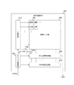
- FIG. 1 is a block diagram illustrating a configuration example of an imaging device 100 according to the first embodiment of the present technology.
- the imaging apparatus 100 is an apparatus for imaging image data, and includes an optical unit 110, a solid-state imaging device 200, and a DSP (Digital Signal Processing) circuit 120. Further, the imaging device 100 includes a display unit 130, an operation unit 140, a bus 150, a frame memory 160, a storage unit 170, and a power supply unit 180.
- a camera mounted on an industrial robot, a vehicle-mounted camera, or the like is assumed.
- the optical unit 110 collects light from a subject and guides the light to the solid-state imaging device 200.
- the solid-state imaging device 200 generates image data by photoelectric conversion.
- the solid-state imaging device 200 generates image data and supplies it to the DSP circuit 120 via a signal line 209.
- the DSP circuit 120 executes predetermined signal processing on image data.
- the DSP circuit 120 outputs the processed image data to the frame memory 160 via the bus 150.
- Note that the DSP circuit 120 is an example of a signal processing unit described in the claims.
- the display unit 130 displays image data.
- a liquid crystal panel or an organic EL (Electro Luminescence) panel is assumed.
- the operation unit 140 generates an operation signal according to a user operation.
- the bus 150 is a common path through which the optical unit 110, the solid-state imaging device 200, the DSP circuit 120, the display unit 130, the operation unit 140, the frame memory 160, the storage unit 170, and the power supply unit 180 exchange data with each other.
- the frame memory 160 stores image data.
- the storage unit 170 stores various data such as image data.
- the power supply unit 180 supplies power to the solid-state imaging device 200, the DSP circuit 120, the display unit 130, and the like.
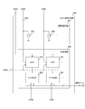
- FIG. 2 is a block diagram illustrating a configuration example of the solid-state imaging device 200 according to the first embodiment of the present technology.
- the solid-state imaging device 200 includes a row selection unit 210, a timing control unit 220, a DAC 230, a pixel array unit 250, a column signal processing unit 260, and a horizontal transfer scanning unit 270. These circuits are arranged on a single semiconductor substrate.
- a plurality of pixels 251 are arranged in a two-dimensional lattice.
- a set of pixels 251 arranged in the horizontal direction is referred to as “row”, and a set of pixels 251 arranged in the vertical direction is referred to as “column”.
- a vertical signal line 259 is wired in the vertical direction for each column. Note that the pixel array section 250 is an example of the pixel section described in the claims.
- the timing control unit 220 controls the operation timing of each of the row selection unit 210, the DAC 230, the column signal processing unit 260, and the horizontal transfer scanning unit 270 in synchronization with the vertical synchronization signal VSYNC.
- the row selection unit 210 sequentially selects and drives the rows in the pixel array unit 250 and outputs pixel signals. Each of the pixels 251 in the selected row outputs an analog pixel signal to the column signal processing unit 260 via the corresponding vertical signal line 259.
- the DAC 230 generates a pair of differential signals that fluctuate with time as a pair of reference signals. For example, a ramp signal is generated as a reference signal.
- the DAC 230 supplies the generated pair of reference signals to the column signal processing unit 260.
- the DAC 230 is an example of a reference signal supply unit described in the claims.
- the column signal processing unit 260 performs processing such as AD conversion and CDS (Correlated Double Sampling) processing on pixel signals for each column.
- the column signal processing unit 260 supplies the DSP circuit 120 with image data composed of the processed digital signal.
- the horizontal transfer scanning unit 270 selects a column in order and causes the column signal processing unit 260 to output a digital signal of the column.
- FIG. 3 is a block diagram illustrating a configuration example of the column signal processing unit 260 according to the first embodiment of the present technology.
- the column signal processing section 260 includes a constant current source circuit 261 and an AD conversion section 300.
- a constant current source 262 is arranged for each column.
- Each constant current source 262 is connected to a vertical signal line 259 of a corresponding column.
- a set including the ADC 310 and the latch circuit 395 is arranged for each column.
- the ADC 310 converts a pixel signal input through the vertical signal line 259 of the corresponding column into a digital signal.
- the ADC 310 outputs the converted digital signal to the latch circuit 395.
- the latch circuit 395 holds the digital signal of the corresponding column.
- the latch circuit 395 outputs the held digital signal to the DSP circuit 120 under the control of the horizontal transfer scanning unit 270.
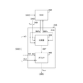
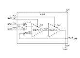
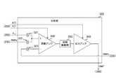
- FIG. 4 is a block diagram illustrating a configuration example of the DAC 230 and the ADC 310 according to the first embodiment of the present technology.
- the ADC 310 includes a comparator 320 and a counter 390.
- DAC 230 outputs the positive signal of the pair of differential signals as reference signal RMPp, and outputs the negative signal as reference signal RMPn.
- reference signals for example, ramp signals are used.
- the comparator 320 compares the comparison target signal corresponding to the value of the pixel signal V vsl based on the reference signal RMPp with the reference signal RMPn. For example, the comparator 320 generates a signal obtained by dividing the difference between the reference signal RMPp and the pixel signal V vsl as a comparison target signal, and compares the signal with the reference signal RMPn. Then, the comparator 320 supplies the comparison result CMP to the counter 390. Note that the circuit constituting the comparator 320 is an example of a comparison unit described in the claims.
- the counter 390 counts a count value in synchronization with the clock signal CLK from the timing control unit 220 until the comparison result CMP is inverted.
- the row selection unit 210 initializes the potential of the pixel signal Vvsl output from the pixels 251 in the selected row to the reset level before the end of the exposure. After the exposure, the row selection unit 210 causes the pixel 251 to output a pixel signal V vsl corresponding to the exposure amount. The potential of the pixel signal V vsl at this time is called a signal level.
- the circuit configuring the counter 390 is an example of the counter unit described in the claims.
- the timing control section 220 causes the counter 390 to initialize the count value by the reset signal RST.
- the counter 390 counts down the count value in synchronization with the clock signal CLK over a period until the comparison result CMP is inverted. Thereby, the reset level is AD-converted.
- the timing control unit 220 inverts the polarity of the increment value using the inversion signal INV.
- the counter 390 counts up the count value in synchronization with the clock signal CLK until the comparison result CMP is inverted. Thereby, the signal level is AD-converted. The count value at the end of the count indicates a difference between the reset level and the signal level. AD conversion and CDS processing are executed by these procedures.
- the counter 390 outputs a digital signal Dout indicating the count value to the latch circuit 395.
- the counter 390 counts down when converting the reset level and counts up when converting the signal level; however, the configuration is not limited to this.
- the counter 390 can count up when converting the reset level and count down when converting the signal level.
- one DAC 230 generates both reference signals RMPp and RMPn.
- a configuration is adopted in which a pair of DACs is arranged, one of which generates the reference signal RMPp, and the other generates the reference signal RMPn. You may.
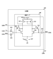
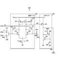
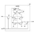
- FIG. 5 is a circuit diagram illustrating a configuration example of the comparator 320 according to the first embodiment of the present technology.
- the comparator 320 includes capacitors 321, 322, and 323 and a differential amplifier 330.
- the pixel signal V vsl is input to one end of the capacitor 321, and the other end is connected to the non-inverting input terminal (+) of the differential amplifier 330.
- the reference signal RMPp is input to one end of the capacitor 322, and the other end is connected to the non-inverting input terminal (+) of the differential amplifier 330 in common with the capacitor 321.
- a signal obtained by dividing the difference between the input pixel signal V vsl and the reference signal RMPp is input to the non-inverting input terminal (+) of the differential amplifier 330.
- the circuit composed of the capacitors 321 and 322 is an example of the input-side voltage dividing circuit described in the claims.
- the reference signal RMPn is input to one end of the capacitor 323, and the other end is connected to the non-inverting input terminal ( ⁇ ) of the differential amplifier 330.
- the differential amplifier 330 amplifies the difference between the signal input to the non-inverting input terminal (+) and the signal input to the inverting input terminal (-).
- the differential amplifier 330 outputs the amplified signal to the counter 390 as a comparison result CMP.
- the differential amplifier 330 receives an auto-zero signal AZ1 from the timing control unit 220.
- the reference signal RMPp is input to one end of the capacitor 322 and the reference signal RMPn is input to one end of the capacitor 323; however, the present invention is not limited to this configuration.
- the reference signal RMPn can be input to one end of the capacitor 322, and the reference signal RMPp can be input to one end of the capacitor 323.
- FIG. 6 is a circuit diagram illustrating a configuration example of the differential amplifier 330 according to the first embodiment of the present technology.
- the differential amplifier 330 includes P-type transistors 331 and 332, N-type transistors 333 to 336, and a current source transistor 337.
- these transistors for example, MOS (Metal-Oxide-Semiconductor) transistors are used.
- MOS Metal-Oxide-Semiconductor
- the current source transistor 337 for example, an N-type MOS transistor is used.
- Sources of the P-type transistors 331 and 332 are commonly connected to a power supply terminal of the power supply potential VDD COM .
- the gate of the P-type transistor 331 is connected to its own drain and the gate of the P-type transistor 332.
- the drain of the N-type transistor 335 is connected to the drain of the P-type transistor 331, the gate is connected to the connection point between the capacitors 321 and 322, and the source is connected to the drain of the current source transistor 337.
- the drain of the N-type transistor 336 is connected to the drain of the P-type transistor 332, the gate is connected to the capacitor 323, and the source is connected to the drain of the current source transistor 337.
- the comparison result CMP is output from the connection point of the P-type transistor 332 and the N-type transistor 336.
- the P-type transistor 332 is an example of a first differential pair transistor described in the appended claims
- the N-type transistor 336 is an example of a second differential pair transistor described in the appended claims. is there.
- a constant bias voltage VbCOM is applied to the gate of the current source transistor 337, and the source is connected to the ground terminal.
- This current source transistor 337 functions as a tail current source.
- the N-type transistor 333 short-circuits the gate and the drain of the N-type transistor 335 according to the auto-zero signal AZ1.
- N-type transistor 334 short-circuits the gate and drain of N-type transistor 336 according to auto-zero signal AZ1. An auto-zero operation is realized by these transistors.
- the differential amplifier 330 outputs a signal at the connection point of the P-type transistor 332 and the N-type transistor 336 as a comparison result CMP, but is not limited to this configuration. As illustrated in FIG. 7, the differential amplifier 330 can output a connection point of the P-type transistor 331 and the N-type transistor 335 as a comparison result CMP. In this case, the gate of the P-type transistor 331 may be connected to the drain and the gate of the P-type transistor 331 without connecting the gate of the P-type transistor 331 to the drain.
- the configuration of the differential amplifier 330 is not limited to the circuits illustrated in FIGS. 6 and 7 as long as the difference between the input terminals can be amplified.
- P-type transistors 335-1 and 336-2 may be arranged instead of N-type transistors 335 and 336.
- N-type transistors 331-1 and 332-2 are provided instead of P-type transistors 331 and 332, and P-type current source transistor 337-1 is provided instead of N-type current source transistor 337.
- the current source transistor 337-1 may be arranged on the power supply side, and the N-type transistors 331-1 and 332-2 may be arranged on the ground side.
- the N-type transistors 333 and 334 are used as switches for controlling the auto-zero operation in FIGS. 6 to 8, a P-type transistor can be used instead of the N-type transistor.
- FIG. 9 is a circuit diagram illustrating a configuration example of the DAC 230 according to the first embodiment of the present technology.
- the DAC 230 includes M (M is an integer) selection circuits 240 and resistors 231 to 233.
- Each of the selection circuits 240 includes a current source 241 and switches 243 and 245.
- the M current sources 241 are connected in parallel to the power supply terminal of the power supply potential VDD DAC .
- the DAC 230 receives an M-bit control signal CTL from the timing control unit 220.
- the m-th (m is an integer of 1 to M ⁇ 1) bit of the control signal CTL is input to the m-th selection circuit 240 as the selection signal CTL_m.
- the current source 241 supplies a predetermined current.
- the switches 243 and 245 output the current from the current source 241 to one of the pair of output terminals according to the corresponding selection signal CTL_m.
- One of the output terminals of the selection circuit 240 is commonly connected to the resistor 231, and the other is commonly connected to the resistor 232.
- the resistors 231 and 232 are commonly connected to one end of the resistor 233.
- the other end of the resistor 233 is connected to a terminal of the reference potential VSS DAC .
- a reference signal RMPp is output from a connection point between the resistor 231 and the selection circuit 240, and a reference signal RMPn is output from a connection point between the resistance 232 and the selection circuit 240.
- each of the selection circuits 240 controlled in accordance with signals CTL, distributing the total current I FS of the M current sources 241 to the resistor 231 side and the resistor 232 side.
- the currents shunted to the resistor 231 and the resistor 232 are added again and flow to the resistor 233, so that the terminal potential of the resistor 233 becomes constant.
- the shunt ratio is k (k is a real number from 0 to 1) and the resistance values of the resistors 231, 232, and 233 are R 1 , R 2, and R 3
- the respective voltages V RMPp and R V RMPn is represented by the following equation.
- V RMPp VSS DAC + R 3 ⁇ I FS + R 1 ⁇ k ⁇ I FS Expression 1
- V RMPn VSS DAC + R 3 ⁇ I FS + R 2 ⁇ (1-k) ⁇ I FS formula 2
- the pixel signal V vsl and the reference signals RMPp and RMPn are input to the differential amplifier 330 via the capacitors 321 to 323. If these capacitors are appropriately initialized to the initial voltage, the DC potentials of the DAC 230, the pixel 251 (including the constant current source 262), and the differential amplifier 330 can be arbitrarily determined. Therefore, there is no problem even if the reference potential VSS DAC is set to 0 volt (V). Further, the potential V CMp of the non-inverting input terminal (+) of the differential amplifier 330 is determined by the voltage division of the capacitors 321 and 322.
- V CMp V vsl ⁇ C 1 / (C 1 + C 2 ) + V RMPp ⁇ C 2 / (C 1 + C 2 )
- V CMn V RMPn Equation 4
- V CMp and V CMn When the potentials V CMp and V CMn become equal, the comparison result CMP is inverted. Assuming that the pixel signal V vsl at this time is V vsleq , the following equations are obtained from Equations 3 and 4.
- V RMPn V vsleq ⁇ C 1 / (C 1 + C 2 ) + V RMPp ⁇ C 2 / (C 1 + C 2 ) Equation 5
- V vsleq R 3 ⁇ I FS + R 2 ⁇ I FS ⁇ (1 + C 2 / C 1 ) -K ⁇ R 1 ⁇ I FS ⁇ C 2 / C 1 + R 2 ⁇ I FS ⁇ (1 + C 2 / C 1 ) ⁇ ... Equation 6
- the amount of change in the potential V vsleq when the shunt ratio k changes from 0 to 1 is obtained.
- This is a value obtained by converting the full scale that is the maximum value of the amplitude of the DAC 230 to the full scale that is the maximum value of the amplitude of the pixel signal V vsl , and this value is referred to as an effective full scale.
- the effective full scale V FS is represented by the following equation.
- V FS R 1 ⁇ I FS ⁇ C 2 / C 1 + R 2 ⁇ I FS ⁇ (1 + C 2 / C 1 ) ⁇
- the DAC 230 supplies a single-ended signal as a reference signal is assumed as a comparative example.
- the capacitor 323 on the inverting input terminal ( ⁇ ) side of the differential amplifier 330 is connected to the ground terminal, and the pixel signal Vvsl is connected to the capacitor 321 on the non-inverting input terminal (+) side of the differential amplifier 330.
- the former effective full scale V FS is represented by only the first term on the right side of Equation 7.
- the latter effective full scale V FS is represented only by the second term on the right side of Equation 7.
- the maximum value of the voltage output from the DAC 230 can be designed to be small in order to realize the target value.
- the power consumption of the DAC 230 can be reduced as compared with the comparative example.
- both the first and second terms are compared with a comparative example using only one of the first and second terms on the right side of Equation 7.
- the current I FS required to achieve the target value can be reduced, whereby the power consumption of the DAC 230 can be reduced as compared with the comparative example.
- the circuit in the DAC 230 is not limited to the circuit illustrated in the figure as long as it can generate the reference signals RMPp and RMPn.
- FIG. 10 is a circuit diagram illustrating a configuration example of the selection circuit 240 according to the first embodiment of the present technology.
- the selection circuit 240 includes a current source transistor 242, selection transistors 244 and 246, and an inverter 247.
- the source of the current source transistor 242 is connected to the power supply terminal, and a constant bias voltage Vb1 is applied to the gate.
- Vb1 is controlled, for example, so that the difference from the power supply potential VDD COM becomes constant.
- the respective sources of the selection transistors 244 and 246 are commonly connected to the drain of the current source transistor 242.
- the drain of the selection transistor 244 is connected to the resistor 231.
- the drain of the selection transistor 246 is connected to the resistor 232, and the selection signal CTL_m is input to the gate.
- the inverter 247 inverts the selection signal CTL_m and supplies the inverted signal to the gate of the selection transistor 244.
- the current source transistor 242 functions as the current source 241 in FIG. 8, and the circuit including the inverter 247 and the selection transistors 244 and 246 functions as the switches 243 and 245 in FIG.
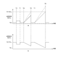
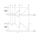
- FIG. 11 is a timing chart illustrating an example of a change in the reference signal according to the first embodiment of the present technology.
- a is a timing chart showing an example of the change of the reference signal RMPp
- b in the figure is a timing chart showing an example of the change of the reference signal RMPn.
- the vertical axis indicates the potential of the reference signal
- the horizontal axis indicates time.
- the solid line a in FIG. 3A indicates the waveform of the reference signal RMPp
- the alternate long and short dash line indicates the waveform of the reference signal of the comparative example.
- the timing control section 220 causes the comparator 320 to perform the auto-zero operation by the auto-zero signal AZ1.
- the DAC 230 when the reset level is output, the DAC 230 generates a reference signal RMPp that increases with the passage of time and a reference signal RMPn that decreases with the passage of time over a period from timing T2 to T3. I do. During this period, the AD conversion of the reset level is performed.
- the amplitudes of reference signal RMPp and reference signal RMPn are set according to the respective capacitance values of capacitors 321, 322, and 323.
- the DAC 230 again generates the reference signal RMPp and the reference signal RMPn over the period from the timing T4 to the timing T5. During this period, AD conversion of the signal level is performed.
- the amplitude of the reference signal necessary to achieve the target value of the effective full-scale V FS is, the case of using the differential signal It will be larger in comparison. Therefore, the power consumption of the DAC increases.
- FIG. 12 is a flowchart illustrating an example of an operation of the solid-state imaging device 200 according to the first embodiment of the present technology. This operation is started, for example, when a predetermined application for capturing image data is executed.
- the row selection unit 210 selects and drives an unselected row (step S901).
- the DAC 230 generates the reference signals RMPp and RMPn (Step S902).
- the ADC 310 AD-converts the reset level (step S903), and AD-converts the signal level (step S904).
- the row selection unit 210 determines whether or not reading of all rows has been completed (step S905). If the reading of all the rows has not been completed (step S905: No), the row selection unit 210 repeatedly executes the steps from step S901. On the other hand, when reading of all rows is completed (step S905: Yes), the row selection unit 210 ends the operation for capturing image data. When a plurality of image data are continuously captured, steps S901 to S905 are repeatedly executed in synchronization with the vertical synchronization signal VSYNC.
- the single-ended signal is used.
- the amplitude of the reference signal can be made smaller.
- the power consumption of the DAC 230 that supplies the reference signal can be reduced.
- the circuits in the solid-state imaging device 200 are arranged on a single semiconductor substrate. However, as the number of pixels increases, the circuit size of the semiconductor substrate increases.
- the solid-state imaging device according to the second embodiment is different from the first embodiment in that circuits in the solid-state imaging device 200 are dispersed and arranged on a plurality of stacked substrates.
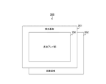
- FIG. 13 is a diagram illustrating an example of a stacked structure of the solid-state imaging device 200 according to the second embodiment of the present technology.
- the solid-state imaging device 200 includes a light receiving substrate 201 and a circuit substrate 202. These substrates are stacked and electrically connected to form one semiconductor chip.
- the pixel array unit 250 is disposed on the light receiving substrate 201. Further, on the circuit board 202, a row selection unit 210, a timing control unit 220, a DAC 230, a column signal processing unit 260, and a horizontal transfer scanning unit 270 are arranged.
- the circuits in the solid-state imaging device 200 are distributed over a plurality of substrates, the circuit scale of each substrate can be reduced.
- FIG. 14 is a circuit diagram illustrating a configuration example of the comparator 320 according to the third embodiment of the present technology.
- the comparator 320 according to the third embodiment differs from the first embodiment in further including an output amplifier 340.
- the output amplifier 340 amplifies the comparison result CMP with a predetermined gain. This output amplifier 340 outputs the amplified signal to the counter 390 as CMP ′.
- the output amplifier 340 receives the auto-zero signal AZ2 from the timing control unit 220.
- FIG. 15 is a circuit diagram illustrating a configuration example of the differential amplifier 330 and the output amplifier 340 according to the third embodiment of the present technology.
- the differential amplifier 330 according to the third embodiment is different from the first embodiment in further including a capacitor 338.
- the output amplifier 340 includes a P-type transistor 341, an N-type transistor 342, a switch 343, and a capacitor 344.
- MOS transistors are used as the P-type transistor 341 and the N-type transistor 342, for example, MOS transistors are used.
- the capacitance 338 is inserted between a connection point of the P-type transistor 332 and the N-type transistor 336 (that is, an output terminal of the differential amplifier 330) and a power supply terminal.
- P-type transistor 341 and N-type transistor 342 are connected in series between a power supply terminal and a ground terminal. Further, the gate of the P-type transistor 341 is connected to the output terminal of the differential amplifier 330, and the comparison result CMP ′ is output from the connection point of the P-type transistor 341 and the N-type transistor 342.
- Capacity 344 is inserted between the gate of N-type transistor 342 and the ground terminal.
- the switch 343 opens and closes a path between the drain and the gate of the N-type transistor 342 according to the auto-zero signal AZ2.
- the output amplifier 340 further amplifies and outputs the output of the differential amplifier 330.
- the output amplifier 340 performs an auto-zero operation according to the auto-zero signal AZ2.
- the output amplifier 340 that further amplifies the output of the differential amplifier 330 is added to the inside of the comparator 320, the driving force of the circuit at the subsequent stage after the counter 390 is reduced. Can increase.
- the output amplifier 340 is further arranged.
- streaking which is streak-like noise, may occur.
- the comparator 320 according to the fourth embodiment differs from the third embodiment in that the amplitude of the output of the differential amplifier 330 is limited to suppress streaking.
- FIG. 16 is a circuit diagram illustrating a configuration example of the comparator 320 according to the fourth embodiment of the present technology.
- the comparator 320 according to the fourth embodiment differs from the third embodiment in further including an amplitude limiting unit 350.
- the amplitude limiter 350 limits the amplitude of the output (comparison result CMP) of the differential amplifier 330 to a certain range and supplies the output to the output amplifier 340.
- FIG. 17 is a circuit diagram illustrating a configuration example of the amplitude limiter 350 according to the fourth embodiment of the present technology.
- the amplitude limiting section 350 includes a bias voltage supply section 351, a current source transistor 352, a common gate transistor 353, and a current source transistor 354.
- a current source transistor 352 for example, a P-type MOS transistor is used.
- a current source transistor 354 for example, an N-type MOS transistor is used.
- the common gate transistor 353, for example, a P-type MOS transistor is used.
- the bias voltage supply unit 351 generates a constant bias voltage and supplies it to the gate of the common-gate transistor 353.
- the current source transistor 352, the common gate transistor 353, and the current source transistor 354 are connected in series between the power supply terminal and the ground terminal.
- the connection point between the current source transistor 352 and the common gate transistor 353 is connected to the output terminal of the differential amplifier 330 on the input side.
- the connection point of the common gate transistor 353 and the current source transistor 354 is connected to the input terminal of the output amplifier 340 on the output side.
- the gate of the current source transistor 352 a constant bias voltage V BLIM1 is applied to the gate of the current source transistor 354, a constant bias voltage V BLIM2 is applied.
- These transistors function as current sources.
- the current source transistor 352 is an example of a power supply side current source described in the claims, and the current source transistor 354 is an example of a ground side current source described in the claims.
- the output of the differential amplifier 330 (comparison result CMP) is limited to a range less than a predetermined upper limit value, and is output to the output amplifier 340.
- the amplitude of the output of the differential amplifier 330 is limited, it is possible to suppress interference between the output and the reference signal RMPn. Thereby, streaking due to the interference can be suppressed.
- the amplitude limiting section 350 is connected to the differential amplifier 330 even when the differential amplifier 330 performs the auto-zero operation.
- the output of the differential amplifier 330 that generates a potential corresponding to the variation or mismatch of the circuit structure or element is directly connected to the source of the gate-grounded transistor 353 whose potential is determined in advance.
- the amplitude limiter of the first modification of the fourth embodiment is different from the first embodiment in that the input of the differential amplifier 330 is cut off during the auto-zero operation.
- FIG. 18 is a circuit diagram illustrating a configuration example of the amplitude limiter 360 according to the first modification of the fourth embodiment of the present technology.
- an amplitude limiting section 360 is arranged instead of the amplitude limiting section 350.
- the amplitude limiter 360 differs from the fourth embodiment in further including switch transistors 361 and 365.
- switch transistors 361 and 365 For example, a P-type MOS transistor is used as the switch transistor 361, and an N-type MOS transistor is used as the switch transistor 365, for example.
- the gates of the switch transistors 361 and 365 are both driven by the auto-zero signal AZ1.
- the bias voltage supply unit 351 includes, for example, P-type transistors 362 and 363 and a current source transistor 364.
- the switch transistor 361 opens and closes a path between the output terminal of the differential amplifier 330 and the connection point of the current source transistor 352 and the common gate transistor 353 according to the auto-zero signal AZ1 from the timing control unit 220.
- the switch transistor 361 is an example of an input-side switch described in the claims.
- the switch transistor 365 opens and closes a path between a connection point of the input terminal of the common-gate transistor 353, the current source transistor 354, and the output terminal of the output amplifier 340 and the ground terminal in accordance with the auto-zero signal AZ1 from the timing control unit 220.
- the switch transistor 365 is an example of an output-side switch described in the claims.
- the P-type transistors 362 and 363 and the current source transistor 364 are connected in series between the power supply terminal and the ground terminal.
- the gate and the drain of the P-type transistor 362 are short-circuited.
- the gate of the common-gate transistor 353 is connected to its own drain and the gate of the P-type transistor 363.
- MOS transistors are used as these transistors.
- a constant bias voltage VbLIM3 is applied to the gate of the current source transistor 364, and the current source transistor 364 functions as a current source.
- the current source transistor 364 for example, an N-type MOS transistor is used.
- the differential amplifier 330 When the auto-zero signal AZ1 is at a high level, the differential amplifier 330 performs an auto-zero operation, and its output generates a potential lower than the power supply potential VDD COM by the gate-source voltage V GS of the N-type transistor 331.
- the bias voltage supply unit 351 sets the source potential of the common-gate transistor 353 to approximately the same potential as the output of the differential amplifier 330 at the time of auto-zero, that is, the potential lowering the power supply potential VDD COM by the gate-source voltage V GS of the N-type transistor 331 Thus, a potential for driving the gate of the common-gate transistor 353 is output.
- the input-side switch transistor 361 is in an open state, and the output-side switch transistor 365 is in a closed state.
- the output of the amplitude limiter 360 is at the ground potential.
- the auto-zero signal AZ1 when the auto-zero signal AZ1 is at a low level, the N-type transistors 333 and 334 in the differential amplifier 330 are turned off, and the differential amplifier 330 performs differential amplification. Further, the input side switch transistor 361 of the amplitude limiter 360 is closed, and the output side switch transistor 365 is opened.
- the source potential of the common-gate transistor 353 determined based on the output of the bias voltage supply unit 351 is set to substantially the same potential as the output of the differential amplifier 330, so that the switch transistor 361 No abnormal current flows in the amplitude limiting section 350 even during a transient phenomenon when the state transitions to the closed state.
- the switch transistor 361 that shuts off the output of the differential amplifier 330 during the auto-zero operation is arranged, the amplitude limiting unit 350 It is possible to prevent occurrence of abnormal current and deterioration of the auto-zero characteristic.
- the output of the differential amplifier 330 is limited to a range less than the upper limit, but it is preferable to set the lower limit.
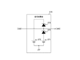
- the amplitude limiter of the second modification of the fourth embodiment is different from the fourth embodiment in that the output of the differential amplifier 330 is limited to a range from a lower limit to an upper limit.
- FIG. 19 is a circuit diagram illustrating a configuration example of the amplitude limiter 370 according to the second modification of the fourth embodiment of the present technology.
- an amplitude limiting section 370 is arranged instead of the amplitude limiting section 350.
- the amplitude limiting section 370 includes bias voltage supply sections 371 and 372 and diodes 373 and 374.
- Diodes 373 and 374 are connected in series between bias voltage supply units 371 and 372.
- the cathode of the diode 373 is connected to the bias voltage supply unit 372, and the anode of the diode 374 is connected to the bias voltage supply unit 371.
- the connection point between the diodes 373 and 374 is connected to the output terminal of the differential amplifier 330 and the input terminal of the output amplifier 340.
- Bias voltage supply unit 371 and 372 is for supplying the different bias voltages V 1 and V 2 together.
- V CMP of the output (comparison result CMP) of the differential amplifier 330 is limited to a range shown by the following equation.
- V F is the forward voltage of the diode 373 and 374.
- the output of the differential amplifier 330 is limited to the range from the lower limit value to the upper limit value. Interference with RMPn can be sufficiently suppressed.
- the output of the differential amplifier 330 is limited to a range less than the upper limit, but it is preferable to set the lower limit.
- the amplitude limiter of the third modification of the fourth embodiment differs from the fourth embodiment in that the output of the differential amplifier 330 is limited to a range from a lower limit to an upper limit.
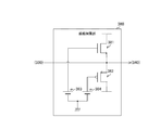
- FIG. 20 is a circuit diagram illustrating a configuration example of the amplitude limiter 380 according to the third modification of the fourth embodiment of the present technology.
- an amplitude limiting section 380 is provided instead of the amplitude limiting section 350.
- the amplitude limiting unit 380 includes an N-type transistor 381, a P-type transistor 382, and bias voltage supply units 383 and 384.
- N-type transistor 381 and P-type transistor 382 are connected in series between a power supply terminal and a ground terminal.
- the connection point between the N-type transistor 381 and the P-type transistor 382 is connected to the output terminal of the differential amplifier 330 and the input terminal of the output amplifier 340.
- Bias voltage supply unit 383 and 384 is for supplying the different bias voltages V 3 and V 4 each other.
- Bias voltage V 3 is applied to the gate of N-type transistor 381
- bias voltage V 4 is applied to the gate of P-type transistor 382.
- the combination of these voltages is set to a value combination in which N-type transistor 381 and P-type transistor 382 are not simultaneously turned on.
- V CMP of the output (comparison result CMP) of the differential amplifier 330 is limited to a range shown by the following equation.
- V 3 ⁇ V GSN ⁇ V CMP ⁇ V 4 + V GSP In the above equation, V GSN is the gate-source voltage of the N-type transistor 381 in the ON state, and V GSP is the gate-source voltage of the P-type transistor 382 in the ON state.
- the output of the differential amplifier 330 is limited to a range from the lower limit value to the upper limit value. Interference with RMPn can be sufficiently suppressed.
- the current is generated by arranging the current source transistor 242 for each selection circuit 240 in the DAC 230.
- the output current of the DAC 230 may be degraded because the drain current value changes according to the characteristics unique to the transistor. Specifically, for example, there is a possibility that the full-scale accuracy and the linearity are deteriorated.
- the DAC 230 according to the fifth embodiment is different from the first embodiment in that cascode transistors are connected to the current source transistor 242 via the selection transistors 244 and 246 to ensure linearity.
- FIG. 21 is a circuit diagram illustrating a configuration example of the selection circuit 240 according to the fifth embodiment of the present technology.
- This selection circuit 240 differs from the first embodiment in further including cascode transistors 248 and 249.
- these transistors for example, P-type MOS transistors are used.
- the source of the cascode transistor 248 is connected to the selection transistor 244, and the drain is connected to the resistor 231 and an output terminal that outputs the reference signal RMPp.
- the source of the cascode transistor 249 is connected to the selection transistor 246, and the drain is connected to the resistor 232 and an output terminal that outputs the reference signal RMPn.
- a bias voltage Vb2 is applied to the gates of the cascode transistors 248 and 249 in order to stabilize the drain-source voltage of the current source transistor 242.
- the current source transistor 242 and the cascode transistor 248 or 249 respond to a change in the total drain-source voltage of each of the transistors that are turned on based on the value of the selection signal CTL_m.
- the gate-source voltage is smaller than that of the first embodiment.
- the cascode transistors 248 and 249 are connected in series to the current source transistor 242 via the selection transistors 244 and 246, the sum of the drain-source voltages thereof is The fluctuation of the drain-source voltage of the current source transistor 242 with respect to the fluctuation of the current source transistor 242 is reduced. As a result, the output accuracy of the DAC 230 can be improved.
- the non-inverting input terminal of the differential amplifier 330 includes a voltage dividing circuit including the capacitors 321 and 322, while the inverting input terminal of the differential amplifier 330 includes a voltage dividing circuit.
- the reference signal RMPp when trying to balance the amplitudes of the inverting and non-inverting input terminals of the differential amplifier 330, it is necessary to make the amplitude of the reference signal RMPp larger than the reference signal RMPn. From the viewpoint of suppressing the interference of the reference signals, it is desirable that the reference signals RMPp and RMPn have high differential symmetry.
- the solid-state imaging device 200 according to the sixth embodiment is different from the first embodiment in that reference signals RMPp and RMPn having high differential symmetry are generated.
- FIG. 22 is a circuit diagram illustrating a configuration example of the comparator 320 according to the sixth embodiment of the present technology.
- the comparator 320 differs from the first embodiment in further including a capacitor 324.
- a predetermined fixed voltage Vc is input to one end of the capacitor 324, and the other end is connected to the inverting input terminal ( ⁇ ) of the differential amplifier 330 in common with the capacitor 323.
- These capacitors 323 and 324 divide the difference between reference signal RMPn and fixed voltage Vc.
- the circuit including the capacitors 323 and 324 is an example of the reference-side voltage dividing circuit described in the claims.
- V CMp V c ⁇ C 4 / (C 3 + C 4 ) + V RMPn ⁇ C 3 / (C 3 + C 4 ) Equation 10
- V vsleq V c ⁇ C 4 (C 1 + C 2 ) / ⁇ (C 3 + C 4 ) C 1 ⁇ + R 3 ⁇ I FS ⁇ C 3 (C 1 + C 2) / ⁇ (C 3 + C 4) C 1 ⁇ -R 3 ⁇ I FS ⁇ C 2 / C 1 + R 2 ⁇ I FS ⁇ C 3 (C 1 + C 2) / ⁇ (C 3 + C 4) C 1 ⁇ -K ⁇ R 1 ⁇ I FS ⁇ C 2 / C 1 ⁇ k ⁇ R 2 ⁇ IFS ⁇ C 3 (C 1 + C 2 ) / ⁇ (C 3 + C 4 ) C 1 ⁇ ... Equation 12
- V FS R 1 ⁇ I FS ⁇ C 2 / C 1 + R 2 ⁇ IFS ⁇ C 3 (C 1 + C 2 ) / ⁇ (C 3 + C 4 ) C 1 ⁇ Equation 13
- the resistance value or the capacitance value can be set to a value satisfying the following expression.
- R 1 R 2 Equation 14
- C 3 / C 4 C 2 / C 1 Equation 15
- Equations 14 and 15 When Equations 14 and 15 are applied to Equations 12 and 13, the following equations are obtained.
- V vsleq V c + R 2 ⁇ I FS ⁇ C 2 / C 1 -k ⁇ 2R 1 ⁇ I FS ⁇ C 2 / C 1
- V FS 2R 1 ⁇ I FS ⁇ C 2 / C 1
- FIG. 23 is a circuit diagram illustrating a configuration example of the DAC 230 according to the sixth embodiment of the present technology.
- the DAC 230 according to the sixth embodiment differs from the first embodiment in further including a fixed voltage generation unit 234.
- the fixed voltage generator 234 generates the fixed voltage Vc and supplies the fixed voltage Vc to the comparator 320.
- the fixed voltage generator 234 is arranged inside the DAC 230, it can be arranged outside the DAC 230.
- FIG. 24 is a timing chart illustrating an example of a change in the reference signal according to the sixth embodiment of the present technology.
- a is a timing chart showing an example of the change of the reference signal RMPp
- b in the figure is a timing chart showing an example of the change of the reference signal RMPn.
- the vertical axis indicates the potential of the reference signal
- the horizontal axis indicates time.
- the symmetry of each waveform of the reference signals RMPp and RMPn is improved as compared with the first embodiment.
- the DAC 230 since the capacitors 321 and 322 and the capacitors 323 and 324 perform the voltage division in the comparator 320, the DAC 230 has the differential symmetry. , Can be supplied. Thus, interference between noise and the like and the reference signal can be suppressed.
- the technology (the present technology) according to the present disclosure can be applied to various products.
- the technology according to the present disclosure is realized as a device mounted on any type of moving object such as an automobile, an electric vehicle, a hybrid electric vehicle, a motorcycle, a bicycle, a personal mobility, an airplane, a drone, a ship, and a robot. You may.
- FIG. 25 is a block diagram illustrating a schematic configuration example of a vehicle control system that is an example of a moving object control system to which the technology according to the present disclosure can be applied.
- Vehicle control system 12000 includes a plurality of electronic control units connected via communication network 12001.
- the vehicle control system 12000 includes a drive system control unit 12010, a body system control unit 12020, an outside information detection unit 12030, an inside information detection unit 12040, and an integrated control unit 12050.
- a microcomputer 12051, an audio / video output unit 12052, and a vehicle-mounted network I / F (interface) 12053 are illustrated.
- the drive system control unit 12010 controls the operation of the device related to the drive system of the vehicle according to various programs.
- the drive system control unit 12010 includes a drive force generation device for generating a drive force of the vehicle such as an internal combustion engine or a drive motor, a drive force transmission mechanism for transmitting the drive force to the wheels, and a steering angle of the vehicle. It functions as a control mechanism such as a steering mechanism for adjusting and a braking device for generating a braking force of the vehicle.
- the body control unit 12020 controls the operation of various devices mounted on the vehicle body according to various programs.
- the body-related control unit 12020 functions as a keyless entry system, a smart key system, a power window device, or a control device for various lamps such as a head lamp, a back lamp, a brake lamp, a blinker, and a fog lamp.
- a radio wave or a signal of various switches transmitted from a portable device replacing the key can be input to the body control unit 12020.
- the body control unit 12020 receives the input of these radio waves or signals and controls a door lock device, a power window device, a lamp, and the like of the vehicle.
- Out-of-vehicle information detection unit 12030 detects information external to the vehicle on which vehicle control system 12000 is mounted.
- an imaging unit 12031 is connected to the outside-of-vehicle information detection unit 12030.
- the out-of-vehicle information detection unit 12030 causes the imaging unit 12031 to capture an image outside the vehicle, and receives the captured image.
- the out-of-vehicle information detection unit 12030 may perform an object detection process or a distance detection process on a person, a vehicle, an obstacle, a sign, or a character on a road surface based on the received image.
- the imaging unit 12031 is an optical sensor that receives light and outputs an electric signal according to the amount of received light.
- the imaging unit 12031 can output an electric signal as an image or can output the information as distance measurement information.
- the light received by the imaging unit 12031 may be visible light or non-visible light such as infrared light.
- the in-vehicle information detection unit 12040 detects information in the vehicle.
- the in-vehicle information detection unit 12040 is connected to, for example, a driver status detection unit 12041 that detects the status of the driver.
- the driver state detection unit 12041 includes, for example, a camera that captures an image of the driver, and the in-vehicle information detection unit 12040 determines the degree of driver fatigue or concentration based on the detection information input from the driver state detection unit 12041. The calculation may be performed, or it may be determined whether the driver has fallen asleep.
- the microcomputer 12051 calculates a control target value of the driving force generation device, the steering mechanism or the braking device based on the information on the inside and outside of the vehicle acquired by the outside information detection unit 12030 or the inside information detection unit 12040, and the drive system control unit A control command can be output to 12010.
- the microcomputer 12051 implements functions of ADAS (Advanced Driver Assistance System) including a collision avoidance or a shock mitigation of a vehicle, a following operation based on a distance between vehicles, a vehicle speed maintaining operation, a vehicle collision warning, or a vehicle lane departure warning. Cooperative control for the purpose.
- ADAS Advanced Driver Assistance System
- the microcomputer 12051 controls the driving force generation device, the steering mechanism, the braking device, and the like based on the information about the surroundings of the vehicle obtained by the outside information detection unit 12030 or the inside information detection unit 12040, so that the driver 120 It is possible to perform cooperative control for automatic driving or the like in which the vehicle travels autonomously without depending on the operation.
- the microcomputer 12051 can output a control command to the body system control unit 12020 based on information on the outside of the vehicle acquired by the outside information detection unit 12030.
- the microcomputer 12051 controls the headlamp according to the position of the preceding vehicle or the oncoming vehicle detected by the outside information detection unit 12030, and performs cooperative control for the purpose of preventing glare such as switching a high beam to a low beam. It can be carried out.
- the sound image output unit 12052 transmits at least one of a sound signal and an image signal to an output device capable of visually or audibly notifying a passenger of the vehicle or the outside of the vehicle of information.
- an audio speaker 12061, a display unit 12062, and an instrument panel 12063 are illustrated as output devices.
- the display unit 12062 may include, for example, at least one of an on-board display and a head-up display.
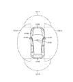
- FIG. 26 is a diagram illustrating an example of an installation position of the imaging unit 12031.
- imaging unit 12031 there are imaging units 12101, 12102, 12103, 12104, and 12105.
- the imaging units 12101, 12102, 12103, 12104, and 12105 are provided, for example, at positions such as a front nose, a side mirror, a rear bumper, a back door, and an upper part of a windshield in the vehicle interior of the vehicle 12100.
- the imaging unit 12101 provided in the front nose and the imaging unit 12105 provided in the upper part of the windshield in the passenger compartment mainly acquire an image in front of the vehicle 12100.
- the imaging units 12102 and 12103 provided in the side mirror mainly acquire images of the side of the vehicle 12100.
- the imaging unit 12104 provided in the rear bumper or the back door mainly acquires an image behind the vehicle 12100.
- the imaging unit 12105 provided above the windshield in the passenger compartment is mainly used for detecting a preceding vehicle or a pedestrian, an obstacle, a traffic light, a traffic sign, a lane, or the like.
- FIG. 26 shows an example of the imaging range of the imaging units 12101 to 12104.
- the imaging range 12111 indicates the imaging range of the imaging unit 12101 provided on the front nose
- the imaging ranges 12112 and 12113 indicate the imaging ranges of the imaging units 12102 and 12103 provided on the side mirrors, respectively
- the imaging range 12114 indicates 13 shows an imaging range of an imaging unit 12104 provided in a rear bumper or a back door. For example, by overlaying image data captured by the imaging units 12101 to 12104, an overhead image of the vehicle 12100 viewed from above can be obtained.
- At least one of the imaging units 12101 to 12104 may have a function of acquiring distance information.
- at least one of the imaging units 12101 to 12104 may be a stereo camera including a plurality of imaging elements or an imaging element having pixels for detecting a phase difference.
- the microcomputer 12051 calculates a distance to each three-dimensional object in the imaging ranges 12111 to 12114 and a temporal change in the distance (relative speed with respect to the vehicle 12100). , It is possible to extract, as a preceding vehicle, a three-dimensional object that travels at a predetermined speed (for example, 0 km / h or more) in the substantially same direction as the vehicle 12100, which is the closest three-dimensional object on the traveling path of the vehicle 12100. it can.
- a predetermined speed for example, 0 km / h or more
- microcomputer 12051 can set an inter-vehicle distance to be secured before the preceding vehicle and perform automatic brake control (including follow-up stop control), automatic acceleration control (including follow-up start control), and the like. In this way, it is possible to perform cooperative control for automatic driving or the like in which the vehicle travels autonomously without depending on the operation of the driver.
- the microcomputer 12051 converts the three-dimensional object data related to the three-dimensional object into other three-dimensional objects such as a two-wheeled vehicle, a normal vehicle, a large vehicle, a pedestrian, and a telephone pole based on the distance information obtained from the imaging units 12101 to 12104. It can be classified and extracted and used for automatic avoidance of obstacles. For example, the microcomputer 12051 distinguishes obstacles around the vehicle 12100 into obstacles that are visible to the driver of the vehicle 12100 and obstacles that are difficult to see. Then, the microcomputer 12051 determines a collision risk indicating a risk of collision with each obstacle, and when the collision risk is equal to or more than the set value and there is a possibility of collision, via the audio speaker 12061 or the display unit 12062. By outputting a warning to the driver through forced driving and avoidance steering via the drive system control unit 12010, driving assistance for collision avoidance can be performed.
- the microcomputer 12051 converts the three-dimensional object data related to the three-dimensional object into other three-dimensional objects such as a
- At least one of the imaging units 12101 to 12104 may be an infrared camera that detects infrared light.
- the microcomputer 12051 can recognize a pedestrian by determining whether or not a pedestrian exists in the captured images of the imaging units 12101 to 12104. The recognition of such a pedestrian is performed by, for example, extracting a feature point in an image captured by the imaging units 12101 to 12104 as an infrared camera, and performing a pattern matching process on a series of feature points indicating the outline of the object to determine whether the object is a pedestrian.
- the audio image output unit 12052 outputs a rectangular outline to the recognized pedestrian for emphasis.
- the display unit 12062 is controlled so that is superimposed. Further, the sound image output unit 12052 may control the display unit 12062 so as to display an icon or the like indicating a pedestrian at a desired position.
- the technology according to the present disclosure can be applied to, for example, the imaging unit 12031 among the configurations described above.
- the imaging device 100 in FIG. 1 can be applied to the imaging unit 12031.
- the power consumption of the imaging unit 12031 can be reduced, so that the power consumption of the entire system can be reduced.
- the present technology may have the following configurations. (1) a pixel unit that outputs a pixel signal based on the amount of incident light; A first reference signal, and a reference signal supply unit that generates a second reference signal, A first differential pair transistor to which a pixel signal and a signal based on the first reference signal are input, and a comparison unit including a second differential pair transistor to which the second reference signal is input, A solid-state imaging device comprising: a counter unit that counts based on a signal from the comparison unit.
- the comparing section includes: An input-side voltage divider circuit that supplies a signal obtained by dividing a difference between the first reference signal and the pixel signal to the first differential pair transistor as a comparison target signal,
- the differential amplifier including the first and second differential pair transistors amplifies a difference between the comparison target signal and the second reference signal and outputs the result of the comparison to the counter unit as the comparison result (1).
- the comparison unit further includes a reference-side voltage dividing circuit that supplies a signal obtained by dividing a difference between the second reference signal and a predetermined fixed potential to the second differential pair transistor,
- the comparison unit further includes an output amplifier that amplifies the comparison result and outputs the result to the counter.
- the comparing unit further includes an amplitude limiting unit that limits an amplitude of the comparison result and supplies the result to the output amplifier.
- the amplitude limiter includes: A pair of bias voltage supply units for supplying mutually different bias voltages, A pair of diodes inserted in series between the pair of bias voltage supply units, The solid-state imaging device according to (5), wherein an output terminal of the differential amplifier and an input terminal of the output amplifier are commonly connected to a connection point of the pair of diodes.
- the amplitude limiter includes: A P-type transistor and an N-type transistor connected in series; A pair of bias voltage supply units for supplying different bias voltages to respective gates of the P-type transistor and the N-type transistor,
- the amplitude limiter includes: A power source side current source connected to the power terminal, A gate-grounded transistor having one end of a source and a drain connected to the power supply-side current source; A bias voltage supply unit that supplies a predetermined bias voltage to the gate of the common-gate transistor; A ground-side current source inserted between the other end of the source and drain of the gate-grounded transistor and a ground terminal, A connection point between one of the power supply-side current source and the ground-side current source and the source of the gate-grounded transistor is connected to an output terminal of the differential amplifier.
- the solid-state imaging device according to (5) wherein a connection point with the drain of the common-gate transistor is connected to an input terminal of the output amplifier.
- the amplitude limiter includes: A connection point between one of the power supply-side current source and the ground-side current source and the source of the gate-grounded transistor, and an input-side switch that opens and closes a path between the output terminal of the differential amplifier and A connection point between the other of the power supply-side current source and the ground-side current source and the drain of the gate-grounded transistor; and an output-side switch that opens and closes a path between the ground terminal and the input-side switch and
- the reference signal supply unit includes: A plurality of selection circuits that output a predetermined current from one of the first and second output terminals according to a predetermined selection signal; A first resistor having one end commonly connected to the first output terminal of each of the plurality of selection circuits; A second resistor having one end commonly connected to the second output terminal of each of the plurality of selection circuits; The above (1) to (9), wherein the first reference signal is output from the one end of the first resistor and the second reference signal is output from the one end of the second resistor.
- the solid-state imaging device according to any one of the preceding claims.
- the selection circuit includes: A current source for supplying the predetermined current; First and second selection transistors commonly connected to the current source; An inverter that inverts the selection signal and supplies the inverted signal to one gate of the first and second selection transistors; A first cascode transistor inserted in series between the first selection transistor and the first output terminal; A second cascode transistor inserted in series between the second selection transistor and the second output terminal; The selection signal is input to the other gates of the first and second selection transistors, and a predetermined bias voltage is applied to respective gates of the first and second cascode transistors (10).
- (12) further comprising a pixel that generates the input signal by photoelectric conversion,
- the pixel is disposed on a predetermined light receiving substrate,
- the solid-state imaging device according to any one of (1) to (11), wherein the reference signal supply unit, the comparison unit, and the counter unit are arranged on a predetermined circuit board stacked on the light receiving substrate.
- a pixel unit that outputs a pixel signal based on the amount of incident light;
- a first reference signal, and a reference signal supply unit that generates a second reference signal,
- a first differential pair transistor to which a pixel signal and a signal based on the first reference signal are input, and a comparison unit including a second differential pair transistor to which the second reference signal is input,
- a counter unit that counts based on the signal of the comparison unit,
- An image pickup apparatus comprising: a signal processing unit that processes a digital signal indicating a count value of the counter unit.
- a reference signal supply procedure for generating a first reference signal and a second reference signal;
- a first differential pair transistor to which a pixel signal based on the amount of incident light and a signal based on the first reference signal are input, and a second differential pair to which the second reference signal is input
- a comparison procedure involving the transistor and a counter procedure for counting based on the signal generated by the comparison procedure.
- Imaging device 110 optical unit 120
- DSP circuit 130 display unit 140 operation unit 150 bus 160 frame memory 170 storage unit 180 power supply unit 200
- solid-state imaging device 201 light receiving substrate 202 circuit substrate 210 row selection unit 220 timing control unit 230 DAC 231, 232, 233 Resistance 234 Fixed voltage generator 240 Selection circuit 241 Current source 242, 337, 337-1, 352, 354, 364 Current source transistor 243, 245, 343 Switch 244, 246 Selection transistor 247 Inverter 248, 249
- Cascode Transistor 250 Pixel array unit 251 Pixel 260
- Constant current source circuit 262 Constant current source 270
- Horizontal transfer scanning unit 300 AD conversion unit 310
Abstract
A solid-state imaging element for performing AD conversion using a reference signal, wherein the power consumption of a circuit that generates the reference signal is reduced. A pixel unit outputs a pixel signal based on the luminous energy of incident light. A reference signal supply unit generates a first reference signal and a second reference signal. A comparison unit includes first differential pair transistors to which a signal based on the pixel signal and the first reference signal are inputted, and second differential pair transistors to which the second reference signal is inputted. A counter unit counts a count value on the basis of a signal from the comparison unit.
Description
本技術は、固体撮像素子、撮像装置、および、固体撮像素子の制御方法に関する。詳しくは、比較器およびカウンタを用いてアナログ信号をデジタル信号に変換する固体撮像素子、撮像装置、および、固体撮像素子の制御方法に関する。
技術 The present technology relates to a solid-state imaging device, an imaging device, and a method for controlling a solid-state imaging device. More specifically, the present invention relates to a solid-state imaging device that converts an analog signal into a digital signal using a comparator and a counter, an imaging device, and a method for controlling the solid-state imaging device.
従来より、固体撮像素子においては、その構造が簡易であるために、シングルスロープ方式のアナログデジタル変換器(ADC:Analog to Digital Converter)が広く用いられている。このシングルスロープ方式のADCは、比較器およびカウンタからなり、比較器は、変換対象の入力信号と所定の参照信号とを比較する。また、そのADC内のカウンタは、比較器の比較結果が反転するまでの期間に亘って計数値を計数し、その計数値を示すデジタル信号を出力する。参照信号としては、ランプ信号などが用いられる。そのランプ信号の振幅が大きいほど、ADCの分解能仕様によって決まるデジタル信号の範囲に対応する入力信号のフルスケールが大きくなる。例えば、列ごとにADCを配置し、DAC(Digital to Analog Converter)がシングルエンド信号を参照信号として生成して、それらをADCに供給する固体撮像素子が提案されている(例えば、特許文献1参照。)。
Conventionally, single-slope analog-to-digital converters (ADCs) have been widely used for solid-state imaging devices because of their simple structure. This single-slope ADC includes a comparator and a counter, and the comparator compares an input signal to be converted with a predetermined reference signal. Further, the counter in the ADC counts the count value until the comparison result of the comparator is inverted, and outputs a digital signal indicating the count value. As the reference signal, a ramp signal or the like is used. As the amplitude of the ramp signal increases, the full scale of the input signal corresponding to the range of the digital signal determined by the resolution specification of the ADC increases. For example, a solid-state imaging device has been proposed in which an ADC is arranged for each column, a DAC (Digital to Analog Converter) generates a single-ended signal as a reference signal, and supplies the reference signal to the ADC (for example, see Patent Document 1). .).
上述の従来技術では、列ごとのADCにより、1行分のアナログ信号を同時にAD変換することができる。しかしながら、参照信号を生成するためのDACの消費電力を低減することが困難である。例えば、参照信号の振幅を小さくすることで、DACの出力電圧の最大値も小さくし、これによって電源電圧も下げることでDACの消費電力を低減しようとしても、DACが出力する参照信号のフルスケールとノイズ実効値の比(PSNR:Peak Signal-to-Noise Ratio)を維持するための消費電流増分が電源電圧を減らした効果を相殺してしまうからである。
(4) In the above-described conventional technology, the analog signals for one row can be simultaneously AD-converted by the ADC for each column. However, it is difficult to reduce the power consumption of the DAC for generating the reference signal. For example, by reducing the amplitude of the reference signal, the maximum value of the output voltage of the DAC is also reduced, thereby reducing the power supply voltage, thereby reducing the power consumption of the DAC. This is because the increase in the current consumption for maintaining the ratio of the noise effective value (PSNR: Peak (Signal-to-Noise Ratio) cancels the effect of reducing the power supply voltage.
本技術はこのような状況に鑑みて生み出されたものであり、参照信号を用いてAD変換を行う固体撮像素子において、参照信号を生成する回路の消費電力を低減することを目的とする。
The present technology has been developed in view of such a situation, and has an object to reduce power consumption of a circuit that generates a reference signal in a solid-state imaging device that performs AD conversion using a reference signal.
本技術は、上述の問題点を解消するためになされたものであり、その第1の側面は、入射光の光量に基づいた画素信号を出力する画素部と、第一の参照信号、および、第二の参照信号を生成する参照信号供給部と、画素信号および上記第一の参照信号に基づいた信号が入力される第一の差動対トランジスタ、および、上記第二の参照信号が入力される第二の差動対トランジスタを含む比較部と、上記比較部の信号に基づいてカウントするカウンタ部とを具備する固体撮像素子、および、その制御方法である。これにより、第一および第二の参照信号と入力信号とから比較結果が生成されるという作用をもたらす。
The present technology has been made to solve the above-described problem, and a first aspect thereof has a pixel unit that outputs a pixel signal based on the amount of incident light, a first reference signal, and A reference signal supply unit that generates a second reference signal, a first differential pair transistor to which a pixel signal and a signal based on the first reference signal are input, and the second reference signal are input. A solid-state imaging device including a comparison unit including a second differential pair transistor, and a counter unit that counts based on a signal of the comparison unit, and a control method thereof. This has the effect that a comparison result is generated from the first and second reference signals and the input signal.
また、この第1の側面において、上記比較部部は、上記第一の参照信号と上記画素信号との差分を分圧した信号を比較対象信号として上記第一の差動対トランジスタに供給する入力側分圧回路をさらに備え、上記第一および第二の差動対トランジスタを含む差動アンプは、上記比較対象信号と上記第二の参照信号との差分を増幅して上記比較結果として上記カウンタ部に出力してもよい。これにより、第一の参照信号と画素信号との差分を分圧した信号が第二参照信号と比較されるという作用をもたらす。
Further, in the first aspect, the comparison unit may include an input that supplies a signal obtained by dividing a difference between the first reference signal and the pixel signal to the first differential pair transistor as a comparison target signal. A differential amplifier including the first and second differential pair transistors, the differential amplifier amplifying a difference between the comparison target signal and the second reference signal, and the counter as a comparison result. It may be output to the unit. This brings about the effect that the signal obtained by dividing the difference between the first reference signal and the pixel signal is compared with the second reference signal.
また、この第1の側面において、上記比較部は、上記第二参照信号と所定の固定電位との差分を分圧した信号を上記第二の差動対トランジスタに供給する参照側分圧回路をさらに備え、上記差動アンプは、上記比較対象信号と上記参照側分圧回路により分圧された信号との差分を増幅してもよい。これにより、差動対称性の高い第一および第二参照信号が供給されるという作用をもたらす。
Further, in the first aspect, the comparing unit includes a reference-side voltage dividing circuit that supplies a signal obtained by dividing a difference between the second reference signal and a predetermined fixed potential to the second differential pair transistor. Further, the differential amplifier may amplify a difference between the comparison target signal and the signal divided by the reference-side voltage dividing circuit. This brings about an effect that the first and second reference signals having high differential symmetry are supplied.
また、この第1の側面において、上記比較部は、上記比較結果を増幅して上記カウンタに出力する出力アンプをさらに備えてもよい。これにより、増幅された信号によってカウンタ以降の回路が駆動されるという作用をもたらす。
In the first aspect, the comparison unit may further include an output amplifier that amplifies the comparison result and outputs the result to the counter. Thus, there is an effect that the circuit after the counter is driven by the amplified signal.
また、この第1の側面において、上記比較部は、上記比較結果の振幅を制限して上記出力アンプに供給する振幅制限部をさらに備えてもよい。これにより、比較結果の振幅が制限されるという作用をもたらす。
In the first aspect, the comparing section may further include an amplitude limiting section that limits the amplitude of the comparison result and supplies the result to the output amplifier. This has the effect of limiting the amplitude of the comparison result.
また、この第1の側面において、上記振幅制限部は、互いに異なるバイアス電圧を供給する一対のバイアス電圧供給部と、上記一対のバイアス電圧供給部の間に直列に挿入された一対のダイオードとを備え、上記差動アンプの出力端子と上記出力アンプの入力端子とは、上記一対のダイオードの接続点に共通に接続されてもよい。これにより、上限値から下限値までの範囲内に振幅が制限されるという作用をもたらす。
Further, in the first aspect, the amplitude limiting section includes a pair of bias voltage supply sections that supply mutually different bias voltages, and a pair of diodes inserted in series between the pair of bias voltage supply sections. The output terminal of the differential amplifier and the input terminal of the output amplifier may be commonly connected to a connection point of the pair of diodes. This brings about an effect that the amplitude is limited within the range from the upper limit to the lower limit.
また、この第1の側面において、上記振幅制限部は、直列に接続されたP型トランジスタおよびN型トランジスタと、互いに異なるバイアス電圧を上記P型トランジスタおよびN型トランジスタのそれぞれのゲートに供給する一対のバイアス電圧供給部とを備え、上記差動アンプの出力端子と上記出力アンプの入力端子とは、上記P型トランジスタおよび上記N型トランジスタの接続点に共通に接続されてもよい。これにより、上限値から下限値までの範囲内に振幅が制限されるという作用をもたらす。
In the first aspect, the amplitude limiter includes a P-type transistor and an N-type transistor connected in series, and a pair of transistors that supply mutually different bias voltages to respective gates of the P-type transistor and the N-type transistor. And an output terminal of the differential amplifier and an input terminal of the output amplifier may be commonly connected to a connection point of the P-type transistor and the N-type transistor. This brings about an effect that the amplitude is limited within the range from the upper limit to the lower limit.
また、この第1の側面において、上記振幅制限部は、電源端子に接続された電源側電流源と、上記電源側電流源にソースおよびドレインの一端が接続されたゲート接地トランジスタと、上記ゲート接地トランジスタのゲートに所定のバイアス電圧を供給するバイアス電圧供給部と、上記ゲート接地トランジスタのソースおよびドレインの他端と接地端子との間に挿入された接地側電流源とを備え、上記電源側電流源および上記接地側電流源の一方と上記ゲート接地トランジスタのソースとの接続点が上記差動アンプの出力端子に接続され、上記電源側電流源および上記接地側電流源の他方と上記ゲート接地トランジスタのドレインとの接続点が上記出力アンプの入力端子に接続されてもよい。これにより、下限値を超える範囲内に振幅が制限されるという作用をもたらす。
Further, in the first aspect, the amplitude limiting section includes: a power supply side current source connected to a power supply terminal; a gate grounded transistor having one end of a source and a drain connected to the power supply side current source; A bias voltage supply unit for supplying a predetermined bias voltage to the gate of the transistor; a ground-side current source inserted between the other end of the source and drain of the gate-grounded transistor and a ground terminal; And a connection point between one of the ground-side current source and the source of the gate-grounded transistor is connected to the output terminal of the differential amplifier, and the other of the power-supply-side current source and the ground-side current source and the gate-grounded transistor May be connected to the input terminal of the output amplifier. This brings about an effect that the amplitude is limited within a range exceeding the lower limit value.
また、この第1の側面において、上記振幅制限部は、上記電源側電流源および上記接地側電流源の一方と上記ゲート接地トランジスタのソースとの接続点と、上記差動アンプの出力端子との間の経路を開閉する入力側スイッチと、上記電源側電流源および上記接地側電流源の他方と上記ゲート接地トランジスタのドレインとの接続点と、上記接地端子との間の経路を開閉する出力側スイッチとをさらに備え、上記入力側スイッチおよび上記出力側スイッチの一方が開状態の場合には他方が閉状態に移行してもよい。これにより、オートゼロ動作中に差動アンプの出力が遮断されるという作用をもたらす。
Further, in the first aspect, the amplitude limiter may include a connection point between one of the power supply-side current source and the ground-side current source and a source of the gate-grounded transistor, and an output terminal of the differential amplifier. An input side switch for opening and closing a path between the power supply side current source and the ground side current source, and a connection point between the drain of the gate grounded transistor and an output side for opening and closing a path between the ground terminal A switch, and when one of the input-side switch and the output-side switch is in an open state, the other may shift to a closed state. This brings about an effect that the output of the differential amplifier is cut off during the auto-zero operation.
また、この第1の側面において、上記参照信号供給部は、所定の選択信号に従って第1および第2の出力端子の一方から所定電流を出力する複数の選択回路と、上記複数の選択回路のそれぞれの上記第1の出力端子に一端が共通に接続された第1の抵抗と、上記複数の選択回路のそれぞれの上記第2の出力端子に一端が共通に接続された第2の抵抗と
を備え、上記第1の抵抗の上記一端から上記第一参照信号が出力され、上記第2の抵抗の上記一端から上記第二の参照信号が出力されてもよい。これにより選択信号に従って第一および第二の参照信号が生成されるという作用をもたらす。 In the first aspect, the reference signal supply unit includes a plurality of selection circuits that output a predetermined current from one of the first and second output terminals according to a predetermined selection signal; A first resistor having one end commonly connected to the first output terminal, and a second resistor having one end commonly connected to each of the second output terminals of the plurality of selection circuits. The first reference signal may be output from the one end of the first resistor, and the second reference signal may be output from the one end of the second resistor. This has an effect that the first and second reference signals are generated according to the selection signal.
を備え、上記第1の抵抗の上記一端から上記第一参照信号が出力され、上記第2の抵抗の上記一端から上記第二の参照信号が出力されてもよい。これにより選択信号に従って第一および第二の参照信号が生成されるという作用をもたらす。 In the first aspect, the reference signal supply unit includes a plurality of selection circuits that output a predetermined current from one of the first and second output terminals according to a predetermined selection signal; A first resistor having one end commonly connected to the first output terminal, and a second resistor having one end commonly connected to each of the second output terminals of the plurality of selection circuits. The first reference signal may be output from the one end of the first resistor, and the second reference signal may be output from the one end of the second resistor. This has an effect that the first and second reference signals are generated according to the selection signal.
また、この第1の側面において、上記選択回路は、上記所定電流を供給する電流源と、上記電流源に共通に接続された第1および第2の選択トランジスタと、上記選択信号を反転させて上記第1および第2の選択トランジスタの一方のゲートに供給するインバータと、上記第1の選択トランジスタと上記第1の出力端子との間に直列に挿入された第1のカスコードトランジスタと、上記第2の選択トランジスタと上記第2の出力端子との間に直列に挿入された第2のカスコードトランジスタとを備え、上記第1および第2の選択トランジスタの他方のゲートには上記選択信号が入力され、上記第1および第2のカスコードトランジスタのそれぞれのゲートには、所定のバイアス電圧が印加されてもよい。これにより、DAC出力の精度が向上するという作用をもたらす。
In the first aspect, the selection circuit may include a current source that supplies the predetermined current, first and second selection transistors commonly connected to the current source, and an inversion of the selection signal. An inverter supplying one of the gates of the first and second selection transistors, a first cascode transistor inserted in series between the first selection transistor and the first output terminal, And a second cascode transistor inserted in series between the second selection transistor and the second output terminal. The selection signal is input to the other gates of the first and second selection transistors. A predetermined bias voltage may be applied to each gate of the first and second cascode transistors. This brings about an effect that the accuracy of the DAC output is improved.
また、この第1の側面において光電変換により上記入力信号を生成する画素をさらに具備し、上記画素は、所定の受光基板に配置され、上記参照信号供給部、上記比較部および上記カウンタ部は、上記受光基板に積層された所定の回路基板に配置されてもよい。これにより、基板当たりの回路規模が削減されるという作用をもたらす。
Further, the first aspect further includes a pixel that generates the input signal by photoelectric conversion, the pixel is disposed on a predetermined light receiving substrate, and the reference signal supply unit, the comparison unit, and the counter unit include: It may be arranged on a predetermined circuit board laminated on the light receiving substrate. This brings about the effect that the circuit scale per board is reduced.
また、本技術の第2の側面は、入射光の光量に基づいた画素信号を出力する画素部と、第一の参照信号、および、第二の参照信号を生成する参照信号供給部と、画素信号および上記第一の参照信号に基づいた信号が入力される第一の差動対トランジスタ、および、上記第二の参照信号が入力される第二の差動対トランジスタを含む比較部と、上記比較部の信号に基づいてカウントするカウンタ部と、上記カウンタ部の計数値を示すデジタル信号を処理する信号処理部とを具備する撮像装置である。これにより、第一および第二の参照信号と入力信号とから比較結果が生成され、その比較結果から生成されたデジタル信号が処理されるという作用をもたらす。
A second aspect of the present technology is directed to a pixel unit that outputs a pixel signal based on the amount of incident light, a first reference signal, and a reference signal supply unit that generates a second reference signal. A first differential pair transistor to which a signal and a signal based on the first reference signal are input, and a comparison unit including a second differential pair transistor to which the second reference signal is input, The imaging apparatus includes a counter unit that counts based on a signal from a comparison unit and a signal processing unit that processes a digital signal indicating a count value of the counter unit. Thereby, the comparison result is generated from the first and second reference signals and the input signal, and the digital signal generated from the comparison result is processed.
本技術によれば、参照信号を用いてAD変換を行う固体撮像素子において、参照信号を生成する回路の消費電力を低減することができるという優れた効果を奏し得る。なお、ここに記載された効果は必ずしも限定されるものではなく、本開示中に記載されたいずれかの効果であってもよい。
According to the present technology, in a solid-state imaging device that performs AD conversion using a reference signal, an excellent effect that power consumption of a circuit that generates the reference signal can be reduced can be achieved. Note that the effects described here are not necessarily limited, and may be any of the effects described in the present disclosure.
以下、本技術を実施するための形態(以下、実施の形態と称する)について説明する。説明は以下の順序により行う。
1.第1の実施の形態(一対の参照信号を比較器に供給する例)
2.第2の実施の形態(積層構造において一対の参照信号を比較器に供給する例)
3.第3の実施の形態(一対の参照信号を比較器に供給し、比較器内に2段のアンプを配置する例)
4.第4の実施の形態(一対の参照信号を比較器に供給し、比較結果の振幅を制限する例)
5.第5の実施の形態(一対の参照信号を比較器に供給し、DAC内にカスコードトランジスタを追加する例)
6.第6の実施の形態(差動対称性の高い一対の参照信号を比較器に供給する例)
7.移動体への応用例 Hereinafter, a mode for implementing the present technology (hereinafter, referred to as an embodiment) will be described. The description will be made in the following order.
1. 1. First embodiment (example of supplying a pair of reference signals to a comparator)
2. 2. Second embodiment (example of supplying a pair of reference signals to a comparator in a stacked structure)
3. 3. Third embodiment (an example in which a pair of reference signals are supplied to a comparator, and a two-stage amplifier is arranged in the comparator)
4. 4. Fourth embodiment (example of supplying a pair of reference signals to a comparator and limiting the amplitude of the comparison result)
5. Fifth embodiment (example in which a pair of reference signals are supplied to a comparator and a cascode transistor is added in a DAC)
6. Sixth embodiment (example of supplying a pair of reference signals having high differential symmetry to a comparator)
7. Example of application to moving objects
<1.第1の実施の形態>
[撮像装置の構成例]
図1は、本技術の第1の実施の形態における撮像装置100の一構成例を示すブロック図である。この撮像装置100は、画像データを撮像するための装置であり、光学部110、固体撮像素子200およびDSP(Digital Signal Processing)回路120を備える。さらに撮像装置100は、表示部130、操作部140、バス150、フレームメモリ160、記憶部170および電源部180を備える。撮像装置100としては、産業用ロボットに搭載されるカメラや、車載カメラなどが想定される。 <1. First Embodiment>
[Configuration Example of Imaging Device]
FIG. 1 is a block diagram illustrating a configuration example of animaging device 100 according to the first embodiment of the present technology. The imaging apparatus 100 is an apparatus for imaging image data, and includes an optical unit 110, a solid-state imaging device 200, and a DSP (Digital Signal Processing) circuit 120. Further, the imaging device 100 includes a display unit 130, an operation unit 140, a bus 150, a frame memory 160, a storage unit 170, and a power supply unit 180. As the imaging device 100, a camera mounted on an industrial robot, a vehicle-mounted camera, or the like is assumed.
[撮像装置の構成例]
図1は、本技術の第1の実施の形態における撮像装置100の一構成例を示すブロック図である。この撮像装置100は、画像データを撮像するための装置であり、光学部110、固体撮像素子200およびDSP(Digital Signal Processing)回路120を備える。さらに撮像装置100は、表示部130、操作部140、バス150、フレームメモリ160、記憶部170および電源部180を備える。撮像装置100としては、産業用ロボットに搭載されるカメラや、車載カメラなどが想定される。 <1. First Embodiment>
[Configuration Example of Imaging Device]
FIG. 1 is a block diagram illustrating a configuration example of an
光学部110は、被写体からの光を集光して固体撮像素子200に導くものである。固体撮像素子200は、光電変換により画像データを生成するものである。この固体撮像素子200は、画像データを生成し、DSP回路120に信号線209を介して供給する。
The optical unit 110 collects light from a subject and guides the light to the solid-state imaging device 200. The solid-state imaging device 200 generates image data by photoelectric conversion. The solid-state imaging device 200 generates image data and supplies it to the DSP circuit 120 via a signal line 209.
DSP回路120は、画像データに対して所定の信号処理を実行するものである。このDSP回路120は、処理後の画像データをバス150を介してフレームメモリ160などに出力する。なお、DSP回路120は、特許請求の範囲に記載の信号処理部の一例である。
The DSP circuit 120 executes predetermined signal processing on image data. The DSP circuit 120 outputs the processed image data to the frame memory 160 via the bus 150. Note that the DSP circuit 120 is an example of a signal processing unit described in the claims.
表示部130は、画像データを表示するものである。表示部130としては、例えば、液晶パネルや有機EL(Electro Luminescence)パネルが想定される。操作部140は、ユーザの操作に従って操作信号を生成するものである。
The display unit 130 displays image data. As the display unit 130, for example, a liquid crystal panel or an organic EL (Electro Luminescence) panel is assumed. The operation unit 140 generates an operation signal according to a user operation.
バス150は、光学部110、固体撮像素子200、DSP回路120、表示部130、操作部140、フレームメモリ160、記憶部170および電源部180が互いにデータをやりとりするための共通の経路である。
The bus 150 is a common path through which the optical unit 110, the solid-state imaging device 200, the DSP circuit 120, the display unit 130, the operation unit 140, the frame memory 160, the storage unit 170, and the power supply unit 180 exchange data with each other.
フレームメモリ160は、画像データを保持するものである。記憶部170は、画像データなどの様々なデータを記憶するものである。電源部180は、固体撮像素子200、DSP回路120や表示部130などに電源を供給するものである。
The frame memory 160 stores image data. The storage unit 170 stores various data such as image data. The power supply unit 180 supplies power to the solid-state imaging device 200, the DSP circuit 120, the display unit 130, and the like.
[固体撮像素子の構成例]
図2は、本技術の第1の実施の形態における固体撮像素子200の一構成例を示すブロック図である。この固体撮像素子200は、行選択部210、タイミング制御部220、DAC230、画素アレイ部250、カラム信号処理部260および水平転送走査部270を備える。これらの回路は、単一の半導体基板に配置される。画素アレイ部250には、複数の画素251が二次元格子状に配列される。以下、水平方向に配列された画素251の集合を「行」と称し、垂直方向に配列された画素251の集合を「列」と称する。また、画素アレイ部250内には、列ごとに垂直方向に垂直信号線259が配線される。なお、画素アレイ部250は、特許請求の範囲に記載の画素部の一例である。 [Configuration example of solid-state imaging device]
FIG. 2 is a block diagram illustrating a configuration example of the solid-state imaging device 200 according to the first embodiment of the present technology. The solid-state imaging device 200 includes a row selection unit 210, a timing control unit 220, a DAC 230, a pixel array unit 250, a column signal processing unit 260, and a horizontal transfer scanning unit 270. These circuits are arranged on a single semiconductor substrate. In the pixel array unit 250, a plurality of pixels 251 are arranged in a two-dimensional lattice. Hereinafter, a set of pixels 251 arranged in the horizontal direction is referred to as “row”, and a set of pixels 251 arranged in the vertical direction is referred to as “column”. Further, in the pixel array section 250, a vertical signal line 259 is wired in the vertical direction for each column. Note that the pixel array section 250 is an example of the pixel section described in the claims.
図2は、本技術の第1の実施の形態における固体撮像素子200の一構成例を示すブロック図である。この固体撮像素子200は、行選択部210、タイミング制御部220、DAC230、画素アレイ部250、カラム信号処理部260および水平転送走査部270を備える。これらの回路は、単一の半導体基板に配置される。画素アレイ部250には、複数の画素251が二次元格子状に配列される。以下、水平方向に配列された画素251の集合を「行」と称し、垂直方向に配列された画素251の集合を「列」と称する。また、画素アレイ部250内には、列ごとに垂直方向に垂直信号線259が配線される。なお、画素アレイ部250は、特許請求の範囲に記載の画素部の一例である。 [Configuration example of solid-state imaging device]
FIG. 2 is a block diagram illustrating a configuration example of the solid-
タイミング制御部220は、垂直同期信号VSYNCに同期して、行選択部210、DAC230、カラム信号処理部260および水平転送走査部270のそれぞれの動作タイミングを制御するものである。
The timing control unit 220 controls the operation timing of each of the row selection unit 210, the DAC 230, the column signal processing unit 260, and the horizontal transfer scanning unit 270 in synchronization with the vertical synchronization signal VSYNC.
行選択部210は、画素アレイ部250内の行を順に選択して駆動し、画素信号を出力させるものである。選択された行内の画素251のそれぞれは、対応する垂直信号線259を介してカラム信号処理部260にアナログの画素信号を出力する。
The row selection unit 210 sequentially selects and drives the rows in the pixel array unit 250 and outputs pixel signals. Each of the pixels 251 in the selected row outputs an analog pixel signal to the column signal processing unit 260 via the corresponding vertical signal line 259.
DAC230は、時間の経過に伴って変動する一対の差動信号を一対の参照信号として生成するものである。例えば、参照信号としてランプ信号が生成される。DAC230は、生成した一対の参照信号をカラム信号処理部260に供給する。なお、DAC230は、特許請求の範囲に記載の参照信号供給部の一例である。
The DAC 230 generates a pair of differential signals that fluctuate with time as a pair of reference signals. For example, a ramp signal is generated as a reference signal. The DAC 230 supplies the generated pair of reference signals to the column signal processing unit 260. The DAC 230 is an example of a reference signal supply unit described in the claims.
カラム信号処理部260は、列ごとに画素信号に対して、AD変換やCDS(Correlated Double Sampling)処理などの処理を行うものである。このカラム信号処理部260は、処理後のデジタル信号からなる画像データをDSP回路120に供給する。
The column signal processing unit 260 performs processing such as AD conversion and CDS (Correlated Double Sampling) processing on pixel signals for each column. The column signal processing unit 260 supplies the DSP circuit 120 with image data composed of the processed digital signal.
水平転送走査部270は、列を順に選択して、その列のデジタル信号をカラム信号処理部260から出力させるものである。
The horizontal transfer scanning unit 270 selects a column in order and causes the column signal processing unit 260 to output a digital signal of the column.
[カラム信号処理部の構成例]
図3は、本技術の第1の実施の形態におけるカラム信号処理部260の一構成例を示すブロック図である。このカラム信号処理部260は、定電流源回路261およびAD変換部300を備える。 [Configuration example of column signal processing unit]
FIG. 3 is a block diagram illustrating a configuration example of the columnsignal processing unit 260 according to the first embodiment of the present technology. The column signal processing section 260 includes a constant current source circuit 261 and an AD conversion section 300.
図3は、本技術の第1の実施の形態におけるカラム信号処理部260の一構成例を示すブロック図である。このカラム信号処理部260は、定電流源回路261およびAD変換部300を備える。 [Configuration example of column signal processing unit]
FIG. 3 is a block diagram illustrating a configuration example of the column
定電流源回路261には、列ごとに定電流源262が配置される。それぞれの定電流源262は、対応する列の垂直信号線259に接続される。
(4) In the constant current source circuit 261, a constant current source 262 is arranged for each column. Each constant current source 262 is connected to a vertical signal line 259 of a corresponding column.
AD変換部300には、ADC310およびラッチ回路395からなる組が列ごとに配置される。
In the A / D converter 300, a set including the ADC 310 and the latch circuit 395 is arranged for each column.
ADC310は、対応する列の垂直信号線259を介して入力された画素信号をデジタル信号に変換するものである。このADC310は、変換後のデジタル信号をラッチ回路395に出力する。
The ADC 310 converts a pixel signal input through the vertical signal line 259 of the corresponding column into a digital signal. The ADC 310 outputs the converted digital signal to the latch circuit 395.
ラッチ回路395は、対応する列のデジタル信号を保持するものである。このラッチ回路395は、保持したデジタル信号を水平転送走査部270の制御に従ってDSP回路120へ出力する。
The latch circuit 395 holds the digital signal of the corresponding column. The latch circuit 395 outputs the held digital signal to the DSP circuit 120 under the control of the horizontal transfer scanning unit 270.
[ADCの構成例]
図4は、本技術の第1の実施の形態におけるDAC230およびADC310の一構成例を示すブロック図である。ADC310は、比較器320およびカウンタ390を備える。 [Configuration Example of ADC]
FIG. 4 is a block diagram illustrating a configuration example of theDAC 230 and the ADC 310 according to the first embodiment of the present technology. The ADC 310 includes a comparator 320 and a counter 390.
図4は、本技術の第1の実施の形態におけるDAC230およびADC310の一構成例を示すブロック図である。ADC310は、比較器320およびカウンタ390を備える。 [Configuration Example of ADC]
FIG. 4 is a block diagram illustrating a configuration example of the
DAC230は、一対の差動信号のうち正側の信号を参照信号RMPpとして出力し、負側の信号を参照信号RMPnとして出力する。これらの参照信号として、例えば、ランプ信号が用いられる。
DAC 230 outputs the positive signal of the pair of differential signals as reference signal RMPp, and outputs the negative signal as reference signal RMPn. As these reference signals, for example, ramp signals are used.
比較器320には、参照信号RMPpを基準とした画素信号Vvslの値に応じた比較対象信号を、参照信号RMPnと比較するものである。例えば、比較器320は、参照信号RMPpと画素信号Vvslとの差分を分圧した信号を比較対象信号として生成し、参照信号RMPnと比較する。そして、比較器320は、比較結果CMPをカウンタ390に供給する。なお、比較器320を構成する回路は、特許請求の範囲に記載の比較部の一例である。
The comparator 320 compares the comparison target signal corresponding to the value of the pixel signal V vsl based on the reference signal RMPp with the reference signal RMPn. For example, the comparator 320 generates a signal obtained by dividing the difference between the reference signal RMPp and the pixel signal V vsl as a comparison target signal, and compares the signal with the reference signal RMPn. Then, the comparator 320 supplies the comparison result CMP to the counter 390. Note that the circuit constituting the comparator 320 is an example of a comparison unit described in the claims.
カウンタ390は、比較結果CMPが反転するまでの期間に亘って、タイミング制御部220からのクロック信号CLKに同期して計数値を計数するものである。ここで、行選択部210は、露光終了の前に、選択した行内の画素251が出力する画素信号Vvslの電位をリセットレベルに初期化する。また、行選択部210は、露光終了後に、露光量に応じた画素信号Vvslを画素251に出力させる。このときの画素信号Vvslの電位は、信号レベルと呼ばれる。なお、カウンタ390を構成する回路は、特許請求の範囲に記載のカウンタ部の一例である。
The counter 390 counts a count value in synchronization with the clock signal CLK from the timing control unit 220 until the comparison result CMP is inverted. Here, the row selection unit 210 initializes the potential of the pixel signal Vvsl output from the pixels 251 in the selected row to the reset level before the end of the exposure. After the exposure, the row selection unit 210 causes the pixel 251 to output a pixel signal V vsl corresponding to the exposure amount. The potential of the pixel signal V vsl at this time is called a signal level. The circuit configuring the counter 390 is an example of the counter unit described in the claims.
タイミング制御部220は、リセットレベルの出力前に、リセット信号RSTによりカウンタ390に計数値を初期化させる。カウンタ390は、比較結果CMPが反転するまでの期間に亘って、クロック信号CLKに同期して計数値をダウンカウントする。これにより、リセットレベルがAD変換される。
(4) Before outputting the reset level, the timing control section 220 causes the counter 390 to initialize the count value by the reset signal RST. The counter 390 counts down the count value in synchronization with the clock signal CLK over a period until the comparison result CMP is inverted. Thereby, the reset level is AD-converted.
そして、タイミング制御部220は、信号レベルの出力直前に、反転信号INVにより増分値の極性を反転させる。カウンタ390は、比較結果CMPが反転するまでの間に亘って、クロック信号CLKに同期して計数値をアップカウントする。これにより、信号レベルがAD変換される。また、計数終了時の計数値は、リセットレベルと信号レベルとの差分を示す。これらの手順により、AD変換およびCDS処理が実行される。カウンタ390は、計数値を示すデジタル信号Doutをラッチ回路395に出力する。
(4) Then, immediately before the output of the signal level, the timing control unit 220 inverts the polarity of the increment value using the inversion signal INV. The counter 390 counts up the count value in synchronization with the clock signal CLK until the comparison result CMP is inverted. Thereby, the signal level is AD-converted. The count value at the end of the count indicates a difference between the reset level and the signal level. AD conversion and CDS processing are executed by these procedures. The counter 390 outputs a digital signal Dout indicating the count value to the latch circuit 395.
なお、カウンタ390は、リセットレベルの変換時にダウンカウントし、信号レベルの変換時にアップカウントしているが、この構成に限定されない。例えば、カウンタ390は、リセットレベルの変換時にアップカウントし、信号レベルの変換時にダウンカウントすることもできる。
Note that the counter 390 counts down when converting the reset level and counts up when converting the signal level; however, the configuration is not limited to this. For example, the counter 390 can count up when converting the reset level and count down when converting the signal level.
また、1つのDAC230が、参照信号RMPpおよびRMPnの両方を生成しているが、一対のDACを配置し、それらの一方が参照信号RMPpを生成し、他方が参照信号RMPnを生成する構成であってもよい。
Further, one DAC 230 generates both reference signals RMPp and RMPn. However, a configuration is adopted in which a pair of DACs is arranged, one of which generates the reference signal RMPp, and the other generates the reference signal RMPn. You may.
[比較器の構成例]
図5は、本技術の第1の実施の形態における比較器320の一構成例を示す回路図である。この比較器320は、容量321、322および323と、差動アンプ330とを備える。 [Comparator configuration example]
FIG. 5 is a circuit diagram illustrating a configuration example of thecomparator 320 according to the first embodiment of the present technology. The comparator 320 includes capacitors 321, 322, and 323 and a differential amplifier 330.
図5は、本技術の第1の実施の形態における比較器320の一構成例を示す回路図である。この比較器320は、容量321、322および323と、差動アンプ330とを備える。 [Comparator configuration example]
FIG. 5 is a circuit diagram illustrating a configuration example of the
容量321の一端には画素信号Vvslが入力され、他端は、差動アンプ330の非反転入力端子(+)に接続される。容量322の一端には参照信号RMPpが入力され、他端は、容量321と共通に差動アンプ330の非反転入力端子(+)に接続される。この接続構成により、差動アンプ330の非反転入力端子(+)には、入力された画素信号Vvslと、参照信号RMPpとの差分を分圧した信号が入力される。なお、容量321および322からなる回路は、特許請求の範囲に記載された入力側分圧回路の一例である。
The pixel signal V vsl is input to one end of the capacitor 321, and the other end is connected to the non-inverting input terminal (+) of the differential amplifier 330. The reference signal RMPp is input to one end of the capacitor 322, and the other end is connected to the non-inverting input terminal (+) of the differential amplifier 330 in common with the capacitor 321. With this connection configuration, a signal obtained by dividing the difference between the input pixel signal V vsl and the reference signal RMPp is input to the non-inverting input terminal (+) of the differential amplifier 330. The circuit composed of the capacitors 321 and 322 is an example of the input-side voltage dividing circuit described in the claims.
また、容量323の一端には、参照信号RMPnが入力され、他端は、差動アンプ330の非反転入力端子(-)に接続される。
{Circle around (1)} The reference signal RMPn is input to one end of the capacitor 323, and the other end is connected to the non-inverting input terminal (−) of the differential amplifier 330.
差動アンプ330は、非反転入力端子(+)に入力された信号と、反転入力端子(-)に入力された信号との差分を増幅するものである。この差動アンプ330は、増幅した信号を比較結果CMPとしてカウンタ390に出力する。また、差動アンプ330には、タイミング制御部220からのオートゼロ信号AZ1が入力される。
(4) The differential amplifier 330 amplifies the difference between the signal input to the non-inverting input terminal (+) and the signal input to the inverting input terminal (-). The differential amplifier 330 outputs the amplified signal to the counter 390 as a comparison result CMP. The differential amplifier 330 receives an auto-zero signal AZ1 from the timing control unit 220.
ここで、DAC230がシングルエンド信号を参照信号として容量322に供給する比較例を想定する。フルスケールを一定とすると、この比較例のDAC230の消費電力は、DAC230が一対の差動信号を供給する構成と比べて大きい。その理由については後述する。
Here, a comparative example in which the DAC 230 supplies a single-ended signal as a reference signal to the capacitor 322 is assumed. Assuming that the full scale is constant, the power consumption of the DAC 230 of this comparative example is larger than that of the configuration in which the DAC 230 supplies a pair of differential signals. The reason will be described later.
なお、容量322の一端に参照信号RMPpを入力し、容量323の一端に参照信号RMPnを入力しているが、この構成に限定されない。例えば、容量322の一端に参照信号RMPnを入力し、容量323の一端に参照信号RMPpを入力することもできる。
Note that the reference signal RMPp is input to one end of the capacitor 322 and the reference signal RMPn is input to one end of the capacitor 323; however, the present invention is not limited to this configuration. For example, the reference signal RMPn can be input to one end of the capacitor 322, and the reference signal RMPp can be input to one end of the capacitor 323.
図6は、本技術の第1の実施の形態における差動アンプ330の一構成例を示す回路図である。この差動アンプ330は、P型トランジスタ331および332と、N型トランジスタ333乃至336と、電流源トランジスタ337とを備える。これらのトランジスタとして、例えば、MOS(Metal-Oxide-Semiconductor)トランジスタが用いられる。電流源トランジスタ337として、例えば、N型のMOSトランジスタが用いられる。
FIG. 6 is a circuit diagram illustrating a configuration example of the differential amplifier 330 according to the first embodiment of the present technology. The differential amplifier 330 includes P- type transistors 331 and 332, N-type transistors 333 to 336, and a current source transistor 337. As these transistors, for example, MOS (Metal-Oxide-Semiconductor) transistors are used. As the current source transistor 337, for example, an N-type MOS transistor is used.
P型トランジスタ331および332のソースは、電源電位VDDCOMの電源端子に共通に接続される。また、P型トランジスタ331のゲートは、自身のドレインと、P型トランジスタ332のゲートとに接続される。
Sources of the P- type transistors 331 and 332 are commonly connected to a power supply terminal of the power supply potential VDD COM . The gate of the P-type transistor 331 is connected to its own drain and the gate of the P-type transistor 332.
N型トランジスタ335のドレインは、P型トランジスタ331のドレインと接続され、ゲートは、容量321および322の接続点に接続され、ソースは電流源トランジスタ337のドレインに接続される。N型トランジスタ336のドレインは、P型トランジスタ332のドレインと接続され、ゲートは、容量323に接続され、ソースは電流源トランジスタ337のドレインに接続される。また、P型トランジスタ332およびN型トランジスタ336の接続点からは、比較結果CMPが出力される。なお、P型トランジスタ332は、特許請求の範囲に記載の第一の差動対トランジスタの一例であり、N型トランジスタ336は、特許請求の範囲に記載の第二の差動対トランジスタの一例である。
The drain of the N-type transistor 335 is connected to the drain of the P-type transistor 331, the gate is connected to the connection point between the capacitors 321 and 322, and the source is connected to the drain of the current source transistor 337. The drain of the N-type transistor 336 is connected to the drain of the P-type transistor 332, the gate is connected to the capacitor 323, and the source is connected to the drain of the current source transistor 337. The comparison result CMP is output from the connection point of the P-type transistor 332 and the N-type transistor 336. The P-type transistor 332 is an example of a first differential pair transistor described in the appended claims, and the N-type transistor 336 is an example of a second differential pair transistor described in the appended claims. is there.
電流源トランジスタ337のゲートには、一定のバイアス電圧VbCOMが印加され、ソースは接地端子に接続される。この電流源トランジスタ337は、テール電流源として機能する。
A constant bias voltage VbCOM is applied to the gate of the current source transistor 337, and the source is connected to the ground terminal. This current source transistor 337 functions as a tail current source.
N型トランジスタ333は、オートゼロ信号AZ1に従ってN型トランジスタ335のゲートおよびドレインを短絡する。N型トランジスタ334は、オートゼロ信号AZ1に従ってN型トランジスタ336のゲートおよびドレインを短絡する。これらのトランジスタにより、オートゼロ動作が実現される。
The N-type transistor 333 short-circuits the gate and the drain of the N-type transistor 335 according to the auto-zero signal AZ1. N-type transistor 334 short-circuits the gate and drain of N-type transistor 336 according to auto-zero signal AZ1. An auto-zero operation is realized by these transistors.
上述の構成により、N型トランジスタ335および336のそれぞれのゲートに入力された信号の差分を増幅した信号が、比較結果CMPとして生成される。
With the above configuration, a signal obtained by amplifying the difference between the signals input to the respective gates of the N- type transistors 335 and 336 is generated as the comparison result CMP.
なお、差動アンプ330は、P型トランジスタ332およびN型トランジスタ336の接続点の信号を比較結果CMPとして出力しているが、この構成に限定されない。差動アンプ330は、図7に例示するようにP型トランジスタ331およびN型トランジスタ335の接続点を比較結果CMPとして出力することもできる。この場合には、P型トランジスタ331のゲートをドレインと接続せず、P型トランジスタ332のゲートを、そのドレインと、P型トランジスタ331のゲートとに接続すればよい。
The differential amplifier 330 outputs a signal at the connection point of the P-type transistor 332 and the N-type transistor 336 as a comparison result CMP, but is not limited to this configuration. As illustrated in FIG. 7, the differential amplifier 330 can output a connection point of the P-type transistor 331 and the N-type transistor 335 as a comparison result CMP. In this case, the gate of the P-type transistor 331 may be connected to the drain and the gate of the P-type transistor 331 without connecting the gate of the P-type transistor 331 to the drain.
また、差動アンプ330の構成は、入力端子間の差分を増幅することができるのであれば、図6や図7に例示した回路に限定されない。例えば、図8に例示するように、N型トランジスタ335および336の代わりにP型トランジスタ335-1および336-2を配置してもよい。この場合には、P型トランジスタ331および332の代わりにN型トランジスタ331-1および332-2が配置され、N型の電流源トランジスタ337の代わりにP型の電流源トランジスタ337-1が配置される。また、この構成では、電流源トランジスタ337-1は電源側に配置され、N型トランジスタ331-1および332-2は接地側に配置すればよい。なお、図6乃至図8においてN型トランジスタ333および334をオートゼロ動作時に制御するスイッチとして用いているが、これらについてもN型トランジスタの代わりにP型トランジスタを用いることもできる。
The configuration of the differential amplifier 330 is not limited to the circuits illustrated in FIGS. 6 and 7 as long as the difference between the input terminals can be amplified. For example, as illustrated in FIG. 8, P-type transistors 335-1 and 336-2 may be arranged instead of N- type transistors 335 and 336. In this case, N-type transistors 331-1 and 332-2 are provided instead of P- type transistors 331 and 332, and P-type current source transistor 337-1 is provided instead of N-type current source transistor 337. You. In this configuration, the current source transistor 337-1 may be arranged on the power supply side, and the N-type transistors 331-1 and 332-2 may be arranged on the ground side. Although the N- type transistors 333 and 334 are used as switches for controlling the auto-zero operation in FIGS. 6 to 8, a P-type transistor can be used instead of the N-type transistor.
[DACの構成例]
図9は、本技術の第1の実施の形態におけるDAC230の一構成例を示す回路図である。このDAC230は、M(Mは、整数)個の選択回路240と、抵抗231乃至233とを備える。選択回路240のそれぞれは、電流源241と、スイッチ243および245とを備える。M個の電流源241は、電源電位VDDDACの電源端子に並列に接続される。また、DAC230には、タイミング制御部220からのMビットの制御信号CTLが入力される。この制御信号CTLのm(mは、1乃至M-1の整数)ビット目は、選択信号CTL_mとして、m個目の選択回路240に入力される。 [Configuration Example of DAC]
FIG. 9 is a circuit diagram illustrating a configuration example of theDAC 230 according to the first embodiment of the present technology. The DAC 230 includes M (M is an integer) selection circuits 240 and resistors 231 to 233. Each of the selection circuits 240 includes a current source 241 and switches 243 and 245. The M current sources 241 are connected in parallel to the power supply terminal of the power supply potential VDD DAC . The DAC 230 receives an M-bit control signal CTL from the timing control unit 220. The m-th (m is an integer of 1 to M−1) bit of the control signal CTL is input to the m-th selection circuit 240 as the selection signal CTL_m.
図9は、本技術の第1の実施の形態におけるDAC230の一構成例を示す回路図である。このDAC230は、M(Mは、整数)個の選択回路240と、抵抗231乃至233とを備える。選択回路240のそれぞれは、電流源241と、スイッチ243および245とを備える。M個の電流源241は、電源電位VDDDACの電源端子に並列に接続される。また、DAC230には、タイミング制御部220からのMビットの制御信号CTLが入力される。この制御信号CTLのm(mは、1乃至M-1の整数)ビット目は、選択信号CTL_mとして、m個目の選択回路240に入力される。 [Configuration Example of DAC]
FIG. 9 is a circuit diagram illustrating a configuration example of the
電流源241は、所定電流を供給するものである。スイッチ243および245は、対応する選択信号CTL_mに従って、一対の出力端子のいずれかに電流源241からの電流を出力するものである。
The current source 241 supplies a predetermined current. The switches 243 and 245 output the current from the current source 241 to one of the pair of output terminals according to the corresponding selection signal CTL_m.
選択回路240のそれぞれの出力端子の一方は、抵抗231に共通に接続され、他方は、抵抗232に共通に接続される。また、抵抗231および232は、抵抗233の一端に共通に接続される。抵抗233の他端は、基準電位VSSDACの端子に接続される。
One of the output terminals of the selection circuit 240 is commonly connected to the resistor 231, and the other is commonly connected to the resistor 232. The resistors 231 and 232 are commonly connected to one end of the resistor 233. The other end of the resistor 233 is connected to a terminal of the reference potential VSS DAC .
抵抗231と選択回路240との接続点からは、参照信号RMPpが出力され、抵抗232と選択回路240との接続点からは、参照信号RMPnが出力される。
A reference signal RMPp is output from a connection point between the resistor 231 and the selection circuit 240, and a reference signal RMPn is output from a connection point between the resistance 232 and the selection circuit 240.
上述の構成により、選択回路240のそれぞれは、制御信号CTLに従って、M個の電流源241の合計電流IFSを抵抗231側と抵抗232側とに振り分ける。抵抗231と抵抗232とのそれぞれに分流した電流は、再び加算されて抵抗233に流れるため、抵抗233の端子電位は一定となる。分流比をk(kは0乃至1の実数)とし、抵抗231、抵抗232および抵抗233の抵抗値をR1、R2およびR3とすると、参照信号RMPpおよびRMPnのそれぞれの電圧VRMPpおよびVRMPnは、次の式により表される。
VRMPp=VSSDAC+R3・IFS+R1・k・IFS ・・・式1
VRMPn=VSSDAC+R3・IFS+R2・(1-k)・IFS …式2 The construction described above, each of theselection circuits 240, controlled in accordance with signals CTL, distributing the total current I FS of the M current sources 241 to the resistor 231 side and the resistor 232 side. The currents shunted to the resistor 231 and the resistor 232 are added again and flow to the resistor 233, so that the terminal potential of the resistor 233 becomes constant. Assuming that the shunt ratio is k (k is a real number from 0 to 1) and the resistance values of the resistors 231, 232, and 233 are R 1 , R 2, and R 3 , the respective voltages V RMPp and R V RMPn is represented by the following equation.
V RMPp = VSS DAC + R 3 · I FS + R 1 · k · I FS Expression 1
V RMPn = VSS DAC + R 3 · I FS + R 2 · (1-k) · I FS formula 2
VRMPp=VSSDAC+R3・IFS+R1・k・IFS ・・・式1
VRMPn=VSSDAC+R3・IFS+R2・(1-k)・IFS …式2 The construction described above, each of the
V RMPp = VSS DAC + R 3 · I FS + R 1 · k · I FS Expression 1
V RMPn = VSS DAC + R 3 · I FS + R 2 · (1-k) · I FS formula 2
ここで、差動アンプ330に容量321乃至323を介して、画素信号Vvslと、参照信号RMPpおよびRMPnが入力されることに着目する。これらの容量が適切に初期電圧に初期化されるのであれば、DAC230と、画素251(定電流源262を含む)と、差動アンプ330との直流電位は任意に決定することができる。このため、基準電位VSSDACを0ボルト(V)としても問題は無い。また、差動アンプ330の非反転入力端子(+)の電位VCMpは、容量321および322の分圧により決定される。容量321および322の容量値をC1およびC2とすると、差動アンプ330の非反転入力端子(+)の電位VCMpは、次の式により表される。
VCMp=Vvsl・C1/(C1+C2)
+VRMPp・C2/(C1+C2) ・・・式3 Here, it is noted that the pixel signal V vsl and the reference signals RMPp and RMPn are input to thedifferential amplifier 330 via the capacitors 321 to 323. If these capacitors are appropriately initialized to the initial voltage, the DC potentials of the DAC 230, the pixel 251 (including the constant current source 262), and the differential amplifier 330 can be arbitrarily determined. Therefore, there is no problem even if the reference potential VSS DAC is set to 0 volt (V). Further, the potential V CMp of the non-inverting input terminal (+) of the differential amplifier 330 is determined by the voltage division of the capacitors 321 and 322. When the capacitance value of the capacitor 321 and 322 and C 1 and C 2, the potential V CMp of the non-inverting input terminal of the differential amplifier 330 (+) is represented by the following equation.
V CMp = V vsl · C 1 / (C 1 + C 2 )
+ V RMPp · C 2 / (C 1 + C 2 )Formula 3
VCMp=Vvsl・C1/(C1+C2)
+VRMPp・C2/(C1+C2) ・・・式3 Here, it is noted that the pixel signal V vsl and the reference signals RMPp and RMPn are input to the
V CMp = V vsl · C 1 / (C 1 + C 2 )
+ V RMPp · C 2 / (C 1 + C 2 )
一方、差動アンプ330の反転入力端子(-)の電位VCMnは、次の式により表される。
VCMn=VRMPn ・・・式4 On the other hand, the potential V CMn of the inverting input terminal (−) of thedifferential amplifier 330 is represented by the following equation.
V CMn = V RMPn Equation 4
VCMn=VRMPn ・・・式4 On the other hand, the potential V CMn of the inverting input terminal (−) of the
V CMn = V RMPn Equation 4
電位VCMpおよびVCMnが等しくなるときに比較結果CMPが反転する。このときの画素信号VvslをVvsleqとすると、式3および式4より次の式が得られる。
VRMPn=Vvsleq・C1/(C1+C2)
+VRMPp・C2/(C1+C2) ・・・式5 When the potentials V CMp and V CMn become equal, the comparison result CMP is inverted. Assuming that the pixel signal V vsl at this time is V vsleq , the following equations are obtained fromEquations 3 and 4.
V RMPn = V vsleq · C 1 / (C 1 + C 2 )
+ V RMPp · C 2 / (C 1 + C 2 ) Equation 5
VRMPn=Vvsleq・C1/(C1+C2)
+VRMPp・C2/(C1+C2) ・・・式5 When the potentials V CMp and V CMn become equal, the comparison result CMP is inverted. Assuming that the pixel signal V vsl at this time is V vsleq , the following equations are obtained from
V RMPn = V vsleq · C 1 / (C 1 + C 2 )
+ V RMPp · C 2 / (C 1 + C 2 ) Equation 5
基準電位VSSDACを0ボルト(V)とし、式5に式1および式2を代入して変形すると、次の式が得られる。
Vvsleq=R3・IFS+R2・IFS・(1+C2/C1)
-k{R1・IFS・C2/C1+R2・IFS・(1+C2/C1)}…式6 When the reference potential VSS DAC is set to 0 volt (V), and the equations (1) and (2) are substituted into the equation (5), the following equation is obtained.
V vsleq = R 3 · I FS + R 2 · I FS · (1 + C 2 / C 1 )
-K {R 1 · I FS · C 2 / C 1 + R 2 · I FS · (1 + C 2 / C 1 )} ... Equation 6
ここで、比較器320が動作可能な信号範囲として、分流比kが0から1に変化した際の電位Vvsleqの変化量を求める。これは、DAC230の振幅の最大値であるフルスケールを、画素信号Vvslの振幅の最大値であるフルスケールに換算した値であり、この値を実効フルスケールと称する。式6より、実効フルスケールVFSは、次の式により表される。
VFS=R1・IFS・C2/C1
+R2・IFS・(1+C2/C1) ・・・式7 Here, as the signal range in which thecomparator 320 can operate, the amount of change in the potential V vsleq when the shunt ratio k changes from 0 to 1 is obtained. This is a value obtained by converting the full scale that is the maximum value of the amplitude of the DAC 230 to the full scale that is the maximum value of the amplitude of the pixel signal V vsl , and this value is referred to as an effective full scale. From Equation 6, the effective full scale V FS is represented by the following equation.
V FS = R 1 · I FS · C 2 / C 1
+ R 2 · I FS · (1 + C 2 / C 1 ) ···
VFS=R1・IFS・C2/C1
+R2・IFS・(1+C2/C1) ・・・式7 Here, as the signal range in which the
V FS = R 1 · I FS · C 2 / C 1
+ R 2 · I FS · (1 + C 2 / C 1 ) ···
ここで、DAC230がシングルエンド信号を参照信号として供給する場合を、比較例として想定する。この比較例では、差動アンプ330の反転入力端子(-)側の容量323を接地端子に接続する構成と、差動アンプ330の非反転入力端子(+)側に画素信号Vvslを容量321と容量322による分圧で生成した比較対象信号を入力する構成の2通りが考えられる。前者の実効フルスケールVFSは、式7右辺の第1項のみにより表される。後者の実効フルスケールVFSは、式7右辺の第2項のみにより表される。実効フルスケールVFSに一定の目標値を設定する場合、式7右辺の第1項および第2項の一方のみを用いる比較例と比較して、第1項および第2項の両方を用いる構成では、その目標値を実現するためDAC230が出力する電圧の最大値を小さく設計できる。それに合わせて電源電圧VDDCOMも小さくすることにより、DAC230の消費電力を比較例よりも低減することができる。
Here, a case where the DAC 230 supplies a single-ended signal as a reference signal is assumed as a comparative example. In this comparative example, the capacitor 323 on the inverting input terminal (−) side of the differential amplifier 330 is connected to the ground terminal, and the pixel signal Vvsl is connected to the capacitor 321 on the non-inverting input terminal (+) side of the differential amplifier 330. There are two possible configurations for inputting the comparison target signal generated by the voltage division by the capacitor 322. The former effective full scale V FS is represented by only the first term on the right side of Equation 7. The latter effective full scale V FS is represented only by the second term on the right side of Equation 7. When setting a constant target value for the effective full scale VFS , a configuration using both the first and second terms as compared with a comparative example using only one of the first and second terms on the right side of Equation 7 Thus, the maximum value of the voltage output from the DAC 230 can be designed to be small in order to realize the target value. By reducing the power supply voltage VDD COM accordingly, the power consumption of the DAC 230 can be reduced as compared with the comparative example.
さらに、実効フルスケールVFSに一定の目標値を設定する場合、式7右辺の第1項か第2項の一方のみを用いる比較例と比較して、第1項および第2項の両方を用いる構成では、その目標値を実現するために要する電流IFSを小さくとることも可能であり、これにより、DAC230の消費電力を比較例よりも低減することができる。
Further, when a constant target value is set for the effective full scale V FS , both the first and second terms are compared with a comparative example using only one of the first and second terms on the right side of Equation 7. In the configuration used, the current I FS required to achieve the target value can be reduced, whereby the power consumption of the DAC 230 can be reduced as compared with the comparative example.
なお、DAC230内の回路は、参照信号RMPpおよびRMPnを生成することができるものであれば、同図に例示した回路に限定されない。
The circuit in the DAC 230 is not limited to the circuit illustrated in the figure as long as it can generate the reference signals RMPp and RMPn.
図10は、本技術の第1の実施の形態における選択回路240の一構成例を示す回路図である。この選択回路240は、電流源トランジスタ242と、選択トランジスタ244および246と、インバータ247とを備える。電流源トランジスタ242、選択トランジスタ244および選択トランジスタ246として、例えば、P型のMOSトランジスタが用いられる。
FIG. 10 is a circuit diagram illustrating a configuration example of the selection circuit 240 according to the first embodiment of the present technology. The selection circuit 240 includes a current source transistor 242, selection transistors 244 and 246, and an inverter 247. As the current source transistor 242, the selection transistor 244, and the selection transistor 246, for example, a P-type MOS transistor is used.
電流源トランジスタ242のソースは、電源端子に接続され、ゲートには一定のバイアス電圧Vb1が印加される。Vb1は、例えば、電源電位VDDCOMとの差が一定になるように制御される。
The source of the current source transistor 242 is connected to the power supply terminal, and a constant bias voltage Vb1 is applied to the gate. Vb1 is controlled, for example, so that the difference from the power supply potential VDD COM becomes constant.
選択トランジスタ244および246のそれぞれのソースは、電流源トランジスタ242のドレインに共通に接続される。また、選択トランジスタ244のドレインは抵抗231に接続される。選択トランジスタ246のドレインは抵抗232に接続され、ゲートには選択信号CTL_mが入力される。
The respective sources of the selection transistors 244 and 246 are commonly connected to the drain of the current source transistor 242. The drain of the selection transistor 244 is connected to the resistor 231. The drain of the selection transistor 246 is connected to the resistor 232, and the selection signal CTL_m is input to the gate.
インバータ247は、選択信号CTL_mを反転して選択トランジスタ244のゲートに供給するものである。
The inverter 247 inverts the selection signal CTL_m and supplies the inverted signal to the gate of the selection transistor 244.
上述の構成により、電流源トランジスタ242は、図8の電流源241として機能し、インバータ247と選択トランジスタ244および246とからなる回路は、図8のスイッチ243および245として機能する。
With the above configuration, the current source transistor 242 functions as the current source 241 in FIG. 8, and the circuit including the inverter 247 and the selection transistors 244 and 246 functions as the switches 243 and 245 in FIG.
図11は、本技術の第1の実施の形態における参照信号の変動の一例を示すタイミングチャートである。同図におけるaは、参照信号RMPpの変動の一例を示すタイミングチャートであり、同図におけるbは、参照信号RMPnの変動の一例を示すタイミングチャートである。同図における縦軸は、参照信号の電位を示し、横軸は時間を示す。また、同図におけるaの実線は、参照信号RMPpの波形を示し、一点鎖線は、比較例の参照信号の波形を示す。
FIG. 11 is a timing chart illustrating an example of a change in the reference signal according to the first embodiment of the present technology. In the figure, a is a timing chart showing an example of the change of the reference signal RMPp, and b in the figure is a timing chart showing an example of the change of the reference signal RMPn. In the figure, the vertical axis indicates the potential of the reference signal, and the horizontal axis indicates time. In addition, the solid line a in FIG. 3A indicates the waveform of the reference signal RMPp, and the alternate long and short dash line indicates the waveform of the reference signal of the comparative example.
露光終了の直前のタイミングT0乃至T1までの期間に亘って、タイミング制御部220は、オートゼロ信号AZ1により比較器320にオートゼロ動作を行わせる。
(4) Over the period from timing T0 to T1 immediately before the end of the exposure, the timing control section 220 causes the comparator 320 to perform the auto-zero operation by the auto-zero signal AZ1.
そして、リセットレベルが出力されるとタイミングT2乃至T3までの期間に亘って、DAC230は、時間の経過に伴って増大する参照信号RMPpと、時間の経過に伴って減少する参照信号RMPnとを生成する。この期間において、リセットレベルのAD変換が行われる。容量321、322および323のそれぞれの容量値に応じて、参照信号RMPpと参照信号RMPnの振幅が設定される。
Then, when the reset level is output, the DAC 230 generates a reference signal RMPp that increases with the passage of time and a reference signal RMPn that decreases with the passage of time over a period from timing T2 to T3. I do. During this period, the AD conversion of the reset level is performed. The amplitudes of reference signal RMPp and reference signal RMPn are set according to the respective capacitance values of capacitors 321, 322, and 323.
また、露光が終了して信号レベルが出力されるとタイミングT4乃至T5までの期間に亘って、DAC230は、再度、参照信号RMPpと参照信号RMPnとを生成する。この期間において、信号レベルのAD変換が行われる。
(4) When the signal level is output after the exposure is completed, the DAC 230 again generates the reference signal RMPp and the reference signal RMPn over the period from the timing T4 to the timing T5. During this period, AD conversion of the signal level is performed.
上述の制御は、行が読み出されるたびに繰り返し実行される。なお、参照信号RMPpがスロープ状に変化する期間と、参照信号RMPnがスロープ状に変化する期間とを一致させているが、この構成に限定されない。例えば、それらの期間の少なくとも一部がオーバーラップする構成であってもよい。
制 御 The above control is repeatedly executed each time a row is read. Note that the period in which the reference signal RMPp changes in a slope shape and the period in which the reference signal RMPn changes in a slope shape are matched, but the present invention is not limited to this configuration. For example, the configuration may be such that at least some of the periods overlap.
同図におけるaに例示するように、シングルエンド信号を参照信号として用いる比較例では、実効フルスケールVFSの目標値を実現するために必要な参照信号の振幅が、差動信号を用いる場合と比較して大きくなる。このため、DACの消費電力が増大してしまう。
As illustrated in a in the figure, in the comparative example used as a reference signal to single-ended signal, the amplitude of the reference signal necessary to achieve the target value of the effective full-scale V FS is, the case of using the differential signal It will be larger in comparison. Therefore, the power consumption of the DAC increases.
[固体撮像素子の動作例]
図12は、本技術の第1の実施の形態における固体撮像素子200の動作の一例を示すフローチャートである。この動作は、例えば、画像データを撮像するための所定のアプリケーションが実行されたときに開始される。 [Operation example of solid-state imaging device]
FIG. 12 is a flowchart illustrating an example of an operation of the solid-state imaging device 200 according to the first embodiment of the present technology. This operation is started, for example, when a predetermined application for capturing image data is executed.
図12は、本技術の第1の実施の形態における固体撮像素子200の動作の一例を示すフローチャートである。この動作は、例えば、画像データを撮像するための所定のアプリケーションが実行されたときに開始される。 [Operation example of solid-state imaging device]
FIG. 12 is a flowchart illustrating an example of an operation of the solid-
行選択部210は、未選択の行を選択して駆動する(ステップS901)。DAC230は、参照信号RMPpおよびRMPnを生成する(ステップS902)。ADC310は、リセットレベルをAD変換し(ステップS903)、信号レベルをAD変換する(ステップS904)。
The row selection unit 210 selects and drives an unselected row (step S901). The DAC 230 generates the reference signals RMPp and RMPn (Step S902). The ADC 310 AD-converts the reset level (step S903), and AD-converts the signal level (step S904).
行選択部210は、全行の読出しが完了したか否かを判断する(ステップS905)。全行の読出しが完了していない場合に(ステップS905:No)、行選択部210は、ステップS901以降を繰り返し実行する。一方、全行の読出しが完了した場合に(ステップS905:Yes)、行選択部210は、画像データを撮像するための動作を終了する。複数枚の画像データを連続して撮像する場合には、ステップS901乃至S905が、垂直同期信号VSYNCに同期して繰り返し実行される。
(4) The row selection unit 210 determines whether or not reading of all rows has been completed (step S905). If the reading of all the rows has not been completed (step S905: No), the row selection unit 210 repeatedly executes the steps from step S901. On the other hand, when reading of all rows is completed (step S905: Yes), the row selection unit 210 ends the operation for capturing image data. When a plurality of image data are continuously captured, steps S901 to S905 are repeatedly executed in synchronization with the vertical synchronization signal VSYNC.
このように、本技術の第1の実施の形態によれば、差動信号の一方(RMPp)を基準とした入力信号の値に応じた信号を他方(RMPn)と比較するため、シングルエンド信号を用いる場合と比較して、参照信号の振幅を小さくすることができる。これにより、参照信号を供給するDAC230の消費電力を低減することができる。
As described above, according to the first embodiment of the present technology, since the signal corresponding to the value of the input signal based on one of the differential signals (RMPp) is compared with the other (RMPn), the single-ended signal is used. , The amplitude of the reference signal can be made smaller. As a result, the power consumption of the DAC 230 that supplies the reference signal can be reduced.
<2.第2の実施の形態>
上述の第1の実施の形態では、固体撮像素子200内の回路を単一の半導体基板に配置していたが、画素数が多くなるほど、半導体基板の回路規模が増大する。この第2の実施の形態の固体撮像素子は、積層された複数の基板に、固体撮像素子200内の回路を分散して配置した点において第1の実施の形態と異なる。 <2. Second Embodiment>
In the first embodiment described above, the circuits in the solid-state imaging device 200 are arranged on a single semiconductor substrate. However, as the number of pixels increases, the circuit size of the semiconductor substrate increases. The solid-state imaging device according to the second embodiment is different from the first embodiment in that circuits in the solid-state imaging device 200 are dispersed and arranged on a plurality of stacked substrates.
上述の第1の実施の形態では、固体撮像素子200内の回路を単一の半導体基板に配置していたが、画素数が多くなるほど、半導体基板の回路規模が増大する。この第2の実施の形態の固体撮像素子は、積層された複数の基板に、固体撮像素子200内の回路を分散して配置した点において第1の実施の形態と異なる。 <2. Second Embodiment>
In the first embodiment described above, the circuits in the solid-
図13は、本技術の第2の実施の形態における固体撮像素子200の積層構造の一例を示す図である。この固体撮像素子200は、受光基板201および回路基板202を備える。これらの基板は積層され、電気的に接続されて1つの半導体チップを構成する。
FIG. 13 is a diagram illustrating an example of a stacked structure of the solid-state imaging device 200 according to the second embodiment of the present technology. The solid-state imaging device 200 includes a light receiving substrate 201 and a circuit substrate 202. These substrates are stacked and electrically connected to form one semiconductor chip.
受光基板201には、画素アレイ部250が配置される。また、回路基板202には、行選択部210、タイミング制御部220、DAC230、カラム信号処理部260および水平転送走査部270が配置される。
画素 The pixel array unit 250 is disposed on the light receiving substrate 201. Further, on the circuit board 202, a row selection unit 210, a timing control unit 220, a DAC 230, a column signal processing unit 260, and a horizontal transfer scanning unit 270 are arranged.
このように、本技術の第2の実施の形態によれば、固体撮像素子200内の回路を複数の基板に分散して配置したため、基板ごとの回路規模を削減することができる。
As described above, according to the second embodiment of the present technology, since the circuits in the solid-state imaging device 200 are distributed over a plurality of substrates, the circuit scale of each substrate can be reduced.
<3.第3の実施の形態>
上述の第1の実施の形態では、比較器320内に増幅回路として差動アンプ330のみを配置していたが、差動アンプ330のみでは、カウンタ390以降の後段の回路の駆動能力が不足するおそれがある。この第3の実施の形態の比較器320は、差動アンプ330の出力を増幅する出力アンプをさらに配置した点において第1の実施の形態と異なる。 <3. Third Embodiment>
In the above-described first embodiment, only thedifferential amplifier 330 is disposed as an amplifier circuit in the comparator 320. However, with only the differential amplifier 330, the driving capability of the circuit subsequent to the counter 390 is insufficient. There is a risk. The comparator 320 according to the third embodiment differs from the first embodiment in that an output amplifier for amplifying the output of the differential amplifier 330 is further provided.
上述の第1の実施の形態では、比較器320内に増幅回路として差動アンプ330のみを配置していたが、差動アンプ330のみでは、カウンタ390以降の後段の回路の駆動能力が不足するおそれがある。この第3の実施の形態の比較器320は、差動アンプ330の出力を増幅する出力アンプをさらに配置した点において第1の実施の形態と異なる。 <3. Third Embodiment>
In the above-described first embodiment, only the
図14は、本技術の第3の実施の形態における比較器320の一構成例を示す回路図である。この第3の実施の形態の比較器320は、出力アンプ340をさらに備える点において第1の実施の形態と異なる。
FIG. 14 is a circuit diagram illustrating a configuration example of the comparator 320 according to the third embodiment of the present technology. The comparator 320 according to the third embodiment differs from the first embodiment in further including an output amplifier 340.
出力アンプ340は、比較結果CMPを所定のゲインにより増幅するものである。この出力アンプ340は、増幅後の信号をCMP'としてカウンタ390に出力する。また、出力アンプ340には、タイミング制御部220からのオートゼロ信号AZ2が入力される。
The output amplifier 340 amplifies the comparison result CMP with a predetermined gain. This output amplifier 340 outputs the amplified signal to the counter 390 as CMP ′. The output amplifier 340 receives the auto-zero signal AZ2 from the timing control unit 220.
図15は、本技術の第3の実施の形態における差動アンプ330および出力アンプ340の一構成例を示す回路図である。第3の実施の形態の差動アンプ330は、容量338をさらに備える点において第1の実施の形態と異なる。また、出力アンプ340は、P型トランジスタ341、N型トランジスタ342、スイッチ343および容量344を備える。P型トランジスタ341およびN型トランジスタ342として、例えば、MOSトランジスタが用いられる。
FIG. 15 is a circuit diagram illustrating a configuration example of the differential amplifier 330 and the output amplifier 340 according to the third embodiment of the present technology. The differential amplifier 330 according to the third embodiment is different from the first embodiment in further including a capacitor 338. The output amplifier 340 includes a P-type transistor 341, an N-type transistor 342, a switch 343, and a capacitor 344. As the P-type transistor 341 and the N-type transistor 342, for example, MOS transistors are used.
容量338は、P型トランジスタ332およびN型トランジスタ336の接続点(すなわち、差動アンプ330の出力端子)と、電源端子との間に挿入される。
The capacitance 338 is inserted between a connection point of the P-type transistor 332 and the N-type transistor 336 (that is, an output terminal of the differential amplifier 330) and a power supply terminal.
P型トランジスタ341およびN型トランジスタ342は、電源端子と接地端子との間において直列に接続される。また、P型トランジスタ341のゲートは、差動アンプ330の出力端子に接続され、P型トランジスタ341およびN型トランジスタ342の接続点から、比較結果CMP'が出力される。
P-type transistor 341 and N-type transistor 342 are connected in series between a power supply terminal and a ground terminal. Further, the gate of the P-type transistor 341 is connected to the output terminal of the differential amplifier 330, and the comparison result CMP ′ is output from the connection point of the P-type transistor 341 and the N-type transistor 342.
容量344は、N型トランジスタ342のゲートと接地端子との間に挿入される。スイッチ343は、オートゼロ信号AZ2に従って、N型トランジスタ342のドレインとゲートとの間の経路を開閉するものである。
Capacity 344 is inserted between the gate of N-type transistor 342 and the ground terminal. The switch 343 opens and closes a path between the drain and the gate of the N-type transistor 342 according to the auto-zero signal AZ2.
上述の構成により、出力アンプ340は、差動アンプ330の出力をさらに増幅して出力する。また、出力アンプ340は、オートゼロ信号AZ2に従ってオートゼロ動作を行う。
With the above configuration, the output amplifier 340 further amplifies and outputs the output of the differential amplifier 330. The output amplifier 340 performs an auto-zero operation according to the auto-zero signal AZ2.
このように、本技術の第3の実施の形態によれば、差動アンプ330の出力をさらに増幅する出力アンプ340を比較器320内に追加したため、カウンタ390以降の後段の回路の駆動力を増大することができる。
As described above, according to the third embodiment of the present technology, since the output amplifier 340 that further amplifies the output of the differential amplifier 330 is added to the inside of the comparator 320, the driving force of the circuit at the subsequent stage after the counter 390 is reduced. Can increase.
<4.第4の実施の形態>
上述の第3の実施の形態では、出力アンプ340をさらに配置していたが、この構成では、筋状のノイズであるストリーキングが生じるおそれがある。これは、差動アンプ330の出力側のN型トランジスタ336のゲートに参照信号RMPnを印加する構成では、差動アンプ330の出力の振幅が大きいと、その参照信号RMPnとの間で干渉が生じてしまうためである。この第4の実施の形態の比較器320は、差動アンプ330の出力の振幅を制限して、ストリーキングを抑制した点において第3の実施の形態と異なる。 <4. Fourth Embodiment>
In the above-described third embodiment, theoutput amplifier 340 is further arranged. However, in this configuration, streaking, which is streak-like noise, may occur. This is because, in the configuration in which the reference signal RMPn is applied to the gate of the N-type transistor 336 on the output side of the differential amplifier 330, if the amplitude of the output of the differential amplifier 330 is large, interference occurs with the reference signal RMPn. This is because The comparator 320 according to the fourth embodiment differs from the third embodiment in that the amplitude of the output of the differential amplifier 330 is limited to suppress streaking.
上述の第3の実施の形態では、出力アンプ340をさらに配置していたが、この構成では、筋状のノイズであるストリーキングが生じるおそれがある。これは、差動アンプ330の出力側のN型トランジスタ336のゲートに参照信号RMPnを印加する構成では、差動アンプ330の出力の振幅が大きいと、その参照信号RMPnとの間で干渉が生じてしまうためである。この第4の実施の形態の比較器320は、差動アンプ330の出力の振幅を制限して、ストリーキングを抑制した点において第3の実施の形態と異なる。 <4. Fourth Embodiment>
In the above-described third embodiment, the
図16は、本技術の第4の実施の形態における比較器320の一構成例を示す回路図である。この第4の実施の形態の比較器320は、振幅制限部350をさらに備える点において第3の実施の形態と異なる。
FIG. 16 is a circuit diagram illustrating a configuration example of the comparator 320 according to the fourth embodiment of the present technology. The comparator 320 according to the fourth embodiment differs from the third embodiment in further including an amplitude limiting unit 350.
振幅制限部350は、差動アンプ330の出力(比較結果CMP)の振幅を、一定範囲内に制限して出力アンプ340に供給するものである。
The amplitude limiter 350 limits the amplitude of the output (comparison result CMP) of the differential amplifier 330 to a certain range and supplies the output to the output amplifier 340.
図17は、本技術の第4の実施の形態における振幅制限部350の一構成例を示す回路図である。この振幅制限部350は、バイアス電圧供給部351、電流源トランジスタ352、ゲート接地トランジスタ353および電流源トランジスタ354を備える。電流源トランジスタ352として、例えば、P型のMOSトランジスタが用いられる。電流源トランジスタ354として、例えば、N型のMOSトランジスタが用いられる。ゲート接地トランジスタ353として、例えば、P型のMOSトランジスタが用いられる。
FIG. 17 is a circuit diagram illustrating a configuration example of the amplitude limiter 350 according to the fourth embodiment of the present technology. The amplitude limiting section 350 includes a bias voltage supply section 351, a current source transistor 352, a common gate transistor 353, and a current source transistor 354. As the current source transistor 352, for example, a P-type MOS transistor is used. As the current source transistor 354, for example, an N-type MOS transistor is used. As the common gate transistor 353, for example, a P-type MOS transistor is used.
バイアス電圧供給部351は、一定のバイアス電圧を生成してゲート接地トランジスタ353のゲートに供給するものである。
The bias voltage supply unit 351 generates a constant bias voltage and supplies it to the gate of the common-gate transistor 353.
電流源トランジスタ352、ゲート接地トランジスタ353および電流源トランジスタ354は、電源端子と接地端子との間に直列に接続される。また、電流源トランジスタ352およびゲート接地トランジスタ353の接続点は、入力側の差動アンプ330の出力端子に接続される。ゲート接地トランジスタ353および電流源トランジスタ354の接続点は、出力側の出力アンプ340の入力端子に接続される。
(4) The current source transistor 352, the common gate transistor 353, and the current source transistor 354 are connected in series between the power supply terminal and the ground terminal. The connection point between the current source transistor 352 and the common gate transistor 353 is connected to the output terminal of the differential amplifier 330 on the input side. The connection point of the common gate transistor 353 and the current source transistor 354 is connected to the input terminal of the output amplifier 340 on the output side.
電流源トランジスタ352のゲートには、一定のバイアス電圧VbLIM1が印加され、電流源トランジスタ354のゲートには、一定のバイアス電圧VbLIM2が印加される。これらのトランジスタは、電流源として機能する。なお、電流源トランジスタ352は、特許請求の範囲に記載の電源側電流源の一例であり、電流源トランジスタ354は、特許請求の範囲に記載の接地側電流源の一例である。
The gate of the current source transistor 352, a constant bias voltage V BLIM1 is applied to the gate of the current source transistor 354, a constant bias voltage V BLIM2 is applied. These transistors function as current sources. The current source transistor 352 is an example of a power supply side current source described in the claims, and the current source transistor 354 is an example of a ground side current source described in the claims.
上述の構成により、差動アンプ330の出力(比較結果CMP)は、所定の上限値未満の範囲内に制限されて、出力アンプ340に出力される。
With the above configuration, the output of the differential amplifier 330 (comparison result CMP) is limited to a range less than a predetermined upper limit value, and is output to the output amplifier 340.
このように、本技術の第4の実施の形態によれば、差動アンプ330の出力の振幅を制限するため、その出力と参照信号RMPnとの間の干渉を抑制することができる。これにより、その干渉に起因するストリーキングを抑制することができる。
As described above, according to the fourth embodiment of the present technology, since the amplitude of the output of the differential amplifier 330 is limited, it is possible to suppress interference between the output and the reference signal RMPn. Thereby, streaking due to the interference can be suppressed.
[第1の変形例]
上述の第4の実施の形態では、差動アンプ330をオートゼロ動作させる際にも振幅制限部350は、差動アンプ330に接続されていた。この構成では、オートゼロ動作期間中、回路構造や素子のばらつきやミスマッチに応じた電位を発生する差動アンプ330の出力が、あらかじめ電位が決まっているゲート接地トランジスタ353のソースに直接接続するため、異常電流が流れることでオートゼロ特性が悪化するおそれある。この第4の実施の形態の第1の変形例の振幅制限部は、オートゼロ動作中に差動アンプ330の入力を遮断する点において第1の実施の形態と異なる。 [First Modification]
In the above-described fourth embodiment, theamplitude limiting section 350 is connected to the differential amplifier 330 even when the differential amplifier 330 performs the auto-zero operation. In this configuration, during the auto-zero operation period, the output of the differential amplifier 330 that generates a potential corresponding to the variation or mismatch of the circuit structure or element is directly connected to the source of the gate-grounded transistor 353 whose potential is determined in advance. When an abnormal current flows, the auto-zero characteristic may be deteriorated. The amplitude limiter of the first modification of the fourth embodiment is different from the first embodiment in that the input of the differential amplifier 330 is cut off during the auto-zero operation.
上述の第4の実施の形態では、差動アンプ330をオートゼロ動作させる際にも振幅制限部350は、差動アンプ330に接続されていた。この構成では、オートゼロ動作期間中、回路構造や素子のばらつきやミスマッチに応じた電位を発生する差動アンプ330の出力が、あらかじめ電位が決まっているゲート接地トランジスタ353のソースに直接接続するため、異常電流が流れることでオートゼロ特性が悪化するおそれある。この第4の実施の形態の第1の変形例の振幅制限部は、オートゼロ動作中に差動アンプ330の入力を遮断する点において第1の実施の形態と異なる。 [First Modification]
In the above-described fourth embodiment, the
図18は、本技術の第4の実施の形態の第1の変形例における振幅制限部360の一構成例を示す回路図である。この第4の実施の形態の第1の変形例では、振幅制限部350の代わりに振幅制限部360が配置される。
FIG. 18 is a circuit diagram illustrating a configuration example of the amplitude limiter 360 according to the first modification of the fourth embodiment of the present technology. In the first modification of the fourth embodiment, an amplitude limiting section 360 is arranged instead of the amplitude limiting section 350.
振幅制限部360は、スイッチトランジスタ361および365をさらに備える点において第4の実施の形態と異なる。スイッチトランジスタ361として、例えば、P型のMOSトランジスタが用いられ、スイッチトランジスタ365として例えば、N型のMOSトランジスタが用いられ、スイッチランジスタ361と365のゲートはともにオートゼロ信号AZ1で駆動される。また、バイアス電圧供給部351は、例えば、P型トランジスタ362および363と電流源トランジスタ364を備える。
The amplitude limiter 360 differs from the fourth embodiment in further including switch transistors 361 and 365. For example, a P-type MOS transistor is used as the switch transistor 361, and an N-type MOS transistor is used as the switch transistor 365, for example. The gates of the switch transistors 361 and 365 are both driven by the auto-zero signal AZ1. The bias voltage supply unit 351 includes, for example, P- type transistors 362 and 363 and a current source transistor 364.
スイッチトランジスタ361は、タイミング制御部220からのオートゼロ信号AZ1に従って、差動アンプ330の出力端子と電流源トランジスタ352およびゲート接地トランジスタ353の接続点との間の経路を開閉するものである。なお、スイッチトランジスタ361は、特許請求の範囲に記載の入力側スイッチの一例である。
The switch transistor 361 opens and closes a path between the output terminal of the differential amplifier 330 and the connection point of the current source transistor 352 and the common gate transistor 353 according to the auto-zero signal AZ1 from the timing control unit 220. Note that the switch transistor 361 is an example of an input-side switch described in the claims.
スイッチトランジスタ365は、タイミング制御部220からのオートゼロ信号AZ1に従って、ゲート接地トランジスタ353、電流源トランジスタ354および出力アンプ340の入力端子の接続点と接地端子との間の経路を開閉するものである。なお、スイッチトランジスタ365は、特許請求の範囲に記載の出力側スイッチの一例である。
The switch transistor 365 opens and closes a path between a connection point of the input terminal of the common-gate transistor 353, the current source transistor 354, and the output terminal of the output amplifier 340 and the ground terminal in accordance with the auto-zero signal AZ1 from the timing control unit 220. The switch transistor 365 is an example of an output-side switch described in the claims.
また、P型トランジスタ362および363と電流源トランジスタ364とは、電源端子と接地端子との間に直列に接続される。P型トランジスタ362のゲートおよびドレインは短絡される。また、ゲート接地トランジスタ353のゲートは、自身のドレインとP型トランジスタ363のゲートとに接続される。これらのトランジスタとして、例えば、MOSトランジスタが用いられる。電流源トランジスタ364のゲートには、一定のバイアス電圧VbLIM3が印加され、電流源トランジスタ364は、電流源として機能する。電流源トランジスタ364としては、例えば、N型のMOSトランジスタが用いられる。
The P- type transistors 362 and 363 and the current source transistor 364 are connected in series between the power supply terminal and the ground terminal. The gate and the drain of the P-type transistor 362 are short-circuited. Further, the gate of the common-gate transistor 353 is connected to its own drain and the gate of the P-type transistor 363. For example, MOS transistors are used as these transistors. A constant bias voltage VbLIM3 is applied to the gate of the current source transistor 364, and the current source transistor 364 functions as a current source. As the current source transistor 364, for example, an N-type MOS transistor is used.
オートゼロ信号AZ1がハイレベルである場合には、差動アンプ330がオートゼロ動作を行い、その出力は、電源電位VDDCOMからN型トランジスタ331のゲート・ソース電圧VGSだけ下がった電位が発生する。バイアス電圧供給部351は、ゲート接地トランジスタ353のソース電位が差動アンプ330のオートゼロ時の出力すなわち電源電位VDDCOMからN型トランジスタ331のゲート・ソース電圧VGSだけ下がった電位と概同電位になるように、ゲート接地トランジスタ353のゲートを駆動する電位を出力する。入力側のスイッチランジスタ361は、開状態となり、出力側のスイッチランジスタ365は閉状態となる。振幅制限部360の出力は接地電位となる。
When the auto-zero signal AZ1 is at a high level, the differential amplifier 330 performs an auto-zero operation, and its output generates a potential lower than the power supply potential VDD COM by the gate-source voltage V GS of the N-type transistor 331. The bias voltage supply unit 351 sets the source potential of the common-gate transistor 353 to approximately the same potential as the output of the differential amplifier 330 at the time of auto-zero, that is, the potential lowering the power supply potential VDD COM by the gate-source voltage V GS of the N-type transistor 331 Thus, a potential for driving the gate of the common-gate transistor 353 is output. The input-side switch transistor 361 is in an open state, and the output-side switch transistor 365 is in a closed state. The output of the amplitude limiter 360 is at the ground potential.
一方、オートゼロ信号AZ1がローレベルである場合には、差動アンプ330内のN型トランジスタ333および334はオフ状態となり、差動アンプ330が差動増幅を行う。また、振幅制限部360の入力側のスイッチトランジスタ361は、閉状態となり、出力側のスイッチトランジスタ365は開状態となる。ここで、オートゼロ信号AZ1がハイレベルのときにバイアス電圧供給部351の出力に基づいて決まるゲート接地トランジスタ353のソース電位は差動アンプ330の出力と概同電位に設定されていたため、スイッチトランジスタ361が閉状態に移行した際の過渡現象時においても、振幅制限部350内に異常電流は流れない。
On the other hand, when the auto-zero signal AZ1 is at a low level, the N- type transistors 333 and 334 in the differential amplifier 330 are turned off, and the differential amplifier 330 performs differential amplification. Further, the input side switch transistor 361 of the amplitude limiter 360 is closed, and the output side switch transistor 365 is opened. Here, when the auto-zero signal AZ1 is at a high level, the source potential of the common-gate transistor 353 determined based on the output of the bias voltage supply unit 351 is set to substantially the same potential as the output of the differential amplifier 330, so that the switch transistor 361 No abnormal current flows in the amplitude limiting section 350 even during a transient phenomenon when the state transitions to the closed state.
このように、本技術の第4の実施の形態の第1の変形例によれば、差動アンプ330がオートゼロ動作中に、その出力を遮断するスイッチトランジスタ361を配置したため、振幅制限部350の異常電流の発生とオートゼロ特性の劣化を防止することができる。
As described above, according to the first modification of the fourth embodiment of the present technology, since the switch transistor 361 that shuts off the output of the differential amplifier 330 during the auto-zero operation is arranged, the amplitude limiting unit 350 It is possible to prevent occurrence of abnormal current and deterioration of the auto-zero characteristic.
[第2の変形例]
上述の第4の実施の形態では、差動アンプ330の出力を上限値未満の範囲内に制限していたが、下限値も設定することが望ましい。この第4の実施の形態の第2の変形例の振幅制限部は、差動アンプ330の出力を、下限値から上限値までの範囲内に制限する点において第4の実施の形態と異なる。 [Second Modification]
In the above-described fourth embodiment, the output of thedifferential amplifier 330 is limited to a range less than the upper limit, but it is preferable to set the lower limit. The amplitude limiter of the second modification of the fourth embodiment is different from the fourth embodiment in that the output of the differential amplifier 330 is limited to a range from a lower limit to an upper limit.
上述の第4の実施の形態では、差動アンプ330の出力を上限値未満の範囲内に制限していたが、下限値も設定することが望ましい。この第4の実施の形態の第2の変形例の振幅制限部は、差動アンプ330の出力を、下限値から上限値までの範囲内に制限する点において第4の実施の形態と異なる。 [Second Modification]
In the above-described fourth embodiment, the output of the
図19は、本技術の第4の実施の形態の第2の変形例における振幅制限部370の一構成例を示す回路図である。この第4の実施の形態の第2の変形例では、振幅制限部350の代わりに振幅制限部370が配置される。
FIG. 19 is a circuit diagram illustrating a configuration example of the amplitude limiter 370 according to the second modification of the fourth embodiment of the present technology. In the second modification of the fourth embodiment, an amplitude limiting section 370 is arranged instead of the amplitude limiting section 350.
振幅制限部370は、バイアス電圧供給部371および372と、ダイオード373および374とを備える。ダイオード373および374は、バイアス電圧供給部371および372の間において直列に接続される。ダイオード373のカソードは、バイアス電圧供給部372に接続され、ダイオード374のアノードは、バイアス電圧供給部371に接続される。また、ダイオード373および374の接続点は、差動アンプ330の出力端子と、出力アンプ340の入力端子とに接続される。
The amplitude limiting section 370 includes bias voltage supply sections 371 and 372 and diodes 373 and 374. Diodes 373 and 374 are connected in series between bias voltage supply units 371 and 372. The cathode of the diode 373 is connected to the bias voltage supply unit 372, and the anode of the diode 374 is connected to the bias voltage supply unit 371. The connection point between the diodes 373 and 374 is connected to the output terminal of the differential amplifier 330 and the input terminal of the output amplifier 340.
バイアス電圧供給部371および372は、互いに異なるバイアス電圧V1およびV2を供給するものである。
Bias voltage supply unit 371 and 372 is for supplying the different bias voltages V 1 and V 2 together.
上述の構成により、差動アンプ330の出力(比較結果CMP)の電圧VCMPは、次の式に示す制限範囲内に制限される。
V1-VF<VCMP<V2+VF
上式において、VFは、ダイオード373および374の順方向電圧である。 With the above-described configuration, the voltage V CMP of the output (comparison result CMP) of thedifferential amplifier 330 is limited to a range shown by the following equation.
V 1 -V F <V CMP <V 2 + V F
In the above equation, V F is the forward voltage of the diode 373 and 374.
V1-VF<VCMP<V2+VF
上式において、VFは、ダイオード373および374の順方向電圧である。 With the above-described configuration, the voltage V CMP of the output (comparison result CMP) of the
V 1 -V F <V CMP <V 2 + V F
In the above equation, V F is the forward voltage of the
このように、本技術の第4の実施の形態の第2の変形例によれば、差動アンプ330の出力を、下限値から上限値までの範囲内に制限するため、その出力と参照信号RMPnとの間の干渉を十分に抑制することができる。
As described above, according to the second modification of the fourth embodiment of the present technology, the output of the differential amplifier 330 is limited to the range from the lower limit value to the upper limit value. Interference with RMPn can be sufficiently suppressed.
[第3の変形例]
上述の第4の実施の形態では、差動アンプ330の出力を上限値未満の範囲内に制限していたが、下限値も設定することが望ましい。この第4の実施の形態の第3の変形例の振幅制限部は、差動アンプ330の出力を、下限値から上限値までの範囲内に制限する点において第4の実施の形態と異なる。 [Third Modification]
In the above-described fourth embodiment, the output of thedifferential amplifier 330 is limited to a range less than the upper limit, but it is preferable to set the lower limit. The amplitude limiter of the third modification of the fourth embodiment differs from the fourth embodiment in that the output of the differential amplifier 330 is limited to a range from a lower limit to an upper limit.
上述の第4の実施の形態では、差動アンプ330の出力を上限値未満の範囲内に制限していたが、下限値も設定することが望ましい。この第4の実施の形態の第3の変形例の振幅制限部は、差動アンプ330の出力を、下限値から上限値までの範囲内に制限する点において第4の実施の形態と異なる。 [Third Modification]
In the above-described fourth embodiment, the output of the
図20は、本技術の第4の実施の形態の第3の変形例における振幅制限部380の一構成例を示す回路図である。この第4の実施の形態の第3の変形例では、振幅制限部350の代わりに振幅制限部380が配置される。
FIG. 20 is a circuit diagram illustrating a configuration example of the amplitude limiter 380 according to the third modification of the fourth embodiment of the present technology. In the third modification of the fourth embodiment, an amplitude limiting section 380 is provided instead of the amplitude limiting section 350.
振幅制限部380は、N型トランジスタ381と、P型トランジスタ382と、バイアス電圧供給部383および384とを備える。
The amplitude limiting unit 380 includes an N-type transistor 381, a P-type transistor 382, and bias voltage supply units 383 and 384.
N型トランジスタ381およびP型トランジスタ382は、電源端子と接地端子との間において直列に接続される。また、N型トランジスタ381およびP型トランジスタ382の接続点は、差動アンプ330の出力端子と、出力アンプ340の入力端子とに接続される。
N-type transistor 381 and P-type transistor 382 are connected in series between a power supply terminal and a ground terminal. The connection point between the N-type transistor 381 and the P-type transistor 382 is connected to the output terminal of the differential amplifier 330 and the input terminal of the output amplifier 340.
バイアス電圧供給部383および384は、互いに異なるバイアス電圧V3およびV4を供給するものである。バイアス電圧V3は、N型トランジスタ381のゲートに印加され、バイアス電圧V4は、P型トランジスタ382のゲートに印加される。これらの電圧の組合せは、N型トランジスタ381およびP型トランジスタ382が同時にオン状態にならない値の組合せに設定される。
Bias voltage supply unit 383 and 384 is for supplying the different bias voltages V 3 and V 4 each other. Bias voltage V 3 is applied to the gate of N-type transistor 381, and bias voltage V 4 is applied to the gate of P-type transistor 382. The combination of these voltages is set to a value combination in which N-type transistor 381 and P-type transistor 382 are not simultaneously turned on.
上述の構成により、差動アンプ330の出力(比較結果CMP)の電圧VCMPは、次の式に示す制限範囲内に制限される。
V3-VGSN<VCMP<V4+VGSP
上式において、VGSNは、オン状態のN型トランジスタ381のゲート・ソース間電圧であり、VGSPは、オン状態のP型トランジスタ382のゲート・ソース間電圧である。 With the above-described configuration, the voltage V CMP of the output (comparison result CMP) of thedifferential amplifier 330 is limited to a range shown by the following equation.
V 3 −V GSN <V CMP <V 4 + V GSP
In the above equation, V GSN is the gate-source voltage of the N-type transistor 381 in the ON state, and V GSP is the gate-source voltage of the P-type transistor 382 in the ON state.
V3-VGSN<VCMP<V4+VGSP
上式において、VGSNは、オン状態のN型トランジスタ381のゲート・ソース間電圧であり、VGSPは、オン状態のP型トランジスタ382のゲート・ソース間電圧である。 With the above-described configuration, the voltage V CMP of the output (comparison result CMP) of the
V 3 −V GSN <V CMP <V 4 + V GSP
In the above equation, V GSN is the gate-source voltage of the N-
このように、本技術の第4の実施の形態の第3の変形例によれば、差動アンプ330の出力を、下限値から上限値までの範囲内に制限するため、その出力と参照信号RMPnとの間の干渉を十分に抑制することができる。
As described above, according to the third modification of the fourth embodiment of the present technology, the output of the differential amplifier 330 is limited to a range from the lower limit value to the upper limit value. Interference with RMPn can be sufficiently suppressed.
<5.第5の実施の形態>
上述の第1の実施の形態では、DAC230内において選択回路240ごとに電流源トランジスタ242を配置して電流を生成していた。しかしながら、電源変動などに起因して、そのトランジスタのドレイン・ソース間電圧が変動すると、トランジスタ固有の特性に応じてドレイン電流値が変化するため、DAC230の出力精度が劣化する恐れがある。具体的には、例えば、フルスケール精度や直線性が劣化する可能性がある。この第5の実施の形態のDAC230は、電流源トランジスタ242に選択トランジスタ244と246とを介してカスコードトランジスタを接続して線形性を確保した点において第1の実施の形態と異なる。 <5. Fifth Embodiment>
In the first embodiment described above, the current is generated by arranging thecurrent source transistor 242 for each selection circuit 240 in the DAC 230. However, if the drain-source voltage of the transistor changes due to a power supply change or the like, the output current of the DAC 230 may be degraded because the drain current value changes according to the characteristics unique to the transistor. Specifically, for example, there is a possibility that the full-scale accuracy and the linearity are deteriorated. The DAC 230 according to the fifth embodiment is different from the first embodiment in that cascode transistors are connected to the current source transistor 242 via the selection transistors 244 and 246 to ensure linearity.
上述の第1の実施の形態では、DAC230内において選択回路240ごとに電流源トランジスタ242を配置して電流を生成していた。しかしながら、電源変動などに起因して、そのトランジスタのドレイン・ソース間電圧が変動すると、トランジスタ固有の特性に応じてドレイン電流値が変化するため、DAC230の出力精度が劣化する恐れがある。具体的には、例えば、フルスケール精度や直線性が劣化する可能性がある。この第5の実施の形態のDAC230は、電流源トランジスタ242に選択トランジスタ244と246とを介してカスコードトランジスタを接続して線形性を確保した点において第1の実施の形態と異なる。 <5. Fifth Embodiment>
In the first embodiment described above, the current is generated by arranging the
図21は、本技術の第5の実施の形態における選択回路240の一構成例を示す回路図である。この選択回路240は、カスコードトランジスタ248および249をさらに備える点において第1の実施の形態と異なる。これらのトランジスタとして、例えば、P型のMOSトランジスタが用いられる。
FIG. 21 is a circuit diagram illustrating a configuration example of the selection circuit 240 according to the fifth embodiment of the present technology. This selection circuit 240 differs from the first embodiment in further including cascode transistors 248 and 249. As these transistors, for example, P-type MOS transistors are used.
カスコードトランジスタ248のソースは、選択トランジスタ244に接続され、ドレインは、抵抗231と、参照信号RMPpを出力する出力端子とに接続される。カスコードトランジスタ249のソースは、選択トランジスタ246に接続され、ドレインは、抵抗232と、参照信号RMPnを出力する出力端子とに接続される。また、カスコードトランジスタ248および249のゲートには、電流源トランジスタ242のドレイン・ソース間電圧を安定化するために、バイアス電圧Vb2が印加される。
The source of the cascode transistor 248 is connected to the selection transistor 244, and the drain is connected to the resistor 231 and an output terminal that outputs the reference signal RMPp. The source of the cascode transistor 249 is connected to the selection transistor 246, and the drain is connected to the resistor 232 and an output terminal that outputs the reference signal RMPn. A bias voltage Vb2 is applied to the gates of the cascode transistors 248 and 249 in order to stabilize the drain-source voltage of the current source transistor 242.
上述の構成において、電流源トランジスタ242と、カスコードトランジスタ248または249内、選択信号CTL_mの値に基づいてONになる方のトランジスタのそれぞれのドレイン・ソース間電圧の合計の変動に対する、電流源トランジスタ242のゲート・ソース間電圧の変動は、第1の実施の形態と比較して小さくなる。これにより、第1の実施の形態と比較してDAC230の出力精度の劣化を小さくすることができる。
In the above-described configuration, the current source transistor 242 and the cascode transistor 248 or 249 respond to a change in the total drain-source voltage of each of the transistors that are turned on based on the value of the selection signal CTL_m. Of the gate-source voltage is smaller than that of the first embodiment. As a result, the deterioration of the output accuracy of the DAC 230 can be reduced as compared with the first embodiment.
このように、本技術の第5の実施の形態によれば、カスコードトランジスタ248および249を選択トランジスタ244と246を介して電流源トランジスタ242に直列に接続したため、それらのドレイン・ソース間電圧の合計の変動に対する、電流源トランジスタ242のドレイン・ソース間電圧の変動が小さくなる。これにより、DAC230の出力精度を向上させることができる。
As described above, according to the fifth embodiment of the present technology, since the cascode transistors 248 and 249 are connected in series to the current source transistor 242 via the selection transistors 244 and 246, the sum of the drain-source voltages thereof is The fluctuation of the drain-source voltage of the current source transistor 242 with respect to the fluctuation of the current source transistor 242 is reduced. As a result, the output accuracy of the DAC 230 can be improved.
<6.第6の実施の形態>
上述の第1の実施の形態では、差動アンプ330の非反転入力端子には容量321、322からなる分圧回路を備える一方、差動アンプ330の反転入力端子には、分圧回路は構成していないため、例えば、差動アンプ330の反転および非反転入力端子の振幅をバランスさせようとすると、参照信号RMPpの振幅を参照信号RMPnよりも大きくする必要があるが、ノイズ等との間の干渉を抑制する観点から、参照信号RMPpおよびRMPnの差動対称性が高いことが望ましい。この第6の実施の形態の固体撮像素子200は、差動対称性の高い参照信号RMPpおよびRMPnを生成する点において第1の実施の形態と異なる。 <6. Sixth embodiment>
In the first embodiment described above, the non-inverting input terminal of thedifferential amplifier 330 includes a voltage dividing circuit including the capacitors 321 and 322, while the inverting input terminal of the differential amplifier 330 includes a voltage dividing circuit. For example, when trying to balance the amplitudes of the inverting and non-inverting input terminals of the differential amplifier 330, it is necessary to make the amplitude of the reference signal RMPp larger than the reference signal RMPn. From the viewpoint of suppressing the interference of the reference signals, it is desirable that the reference signals RMPp and RMPn have high differential symmetry. The solid-state imaging device 200 according to the sixth embodiment is different from the first embodiment in that reference signals RMPp and RMPn having high differential symmetry are generated.
上述の第1の実施の形態では、差動アンプ330の非反転入力端子には容量321、322からなる分圧回路を備える一方、差動アンプ330の反転入力端子には、分圧回路は構成していないため、例えば、差動アンプ330の反転および非反転入力端子の振幅をバランスさせようとすると、参照信号RMPpの振幅を参照信号RMPnよりも大きくする必要があるが、ノイズ等との間の干渉を抑制する観点から、参照信号RMPpおよびRMPnの差動対称性が高いことが望ましい。この第6の実施の形態の固体撮像素子200は、差動対称性の高い参照信号RMPpおよびRMPnを生成する点において第1の実施の形態と異なる。 <6. Sixth embodiment>
In the first embodiment described above, the non-inverting input terminal of the
図22は、本技術の第6の実施の形態における比較器320の一構成例を示す回路図である。この比較器320は、容量324をさらに備える点において第1の実施の形態と異なる。容量324の一端には、所定の固定電圧Vcが入力され、他端は、容量323と共通に差動アンプ330の反転入力端子(-)に接続される。これらの容量323および324により、参照信号RMPnと固定電圧Vcとの差分が分圧される。なお、容量323および324からなる回路は、特許請求の範囲に記載の参照側分圧回路の一例である。
FIG. 22 is a circuit diagram illustrating a configuration example of the comparator 320 according to the sixth embodiment of the present technology. The comparator 320 differs from the first embodiment in further including a capacitor 324. A predetermined fixed voltage Vc is input to one end of the capacitor 324, and the other end is connected to the inverting input terminal (−) of the differential amplifier 330 in common with the capacitor 323. These capacitors 323 and 324 divide the difference between reference signal RMPn and fixed voltage Vc. The circuit including the capacitors 323 and 324 is an example of the reference-side voltage dividing circuit described in the claims.
差動アンプ330の非反転入力端子(+)の電位VCMpは、第1の実施の形態と同様に式3により表される。一方、容量323および324の容量値をC3およびC4とすると、差動アンプ330の反転入力端子(-)の電位VCMnは、次の式により表される。
VCMn=Vc・C4/(C3+C4)
+VRMPn・C3/(C3+C4) ・・・式10 The potential V CMp of the non-inverting input terminal (+) of thedifferential amplifier 330 is expressed by Expression 3 as in the first embodiment. On the other hand, assuming that the capacitance values of the capacitors 323 and 324 are C 3 and C 4 , the potential V CMn of the inverting input terminal (−) of the differential amplifier 330 is represented by the following equation.
V CMn = V c · C 4 / (C 3 + C 4 )
+ V RMPn · C 3 / (C 3 + C 4 ) Equation 10
VCMn=Vc・C4/(C3+C4)
+VRMPn・C3/(C3+C4) ・・・式10 The potential V CMp of the non-inverting input terminal (+) of the
V CMn = V c · C 4 / (C 3 + C 4 )
+ V RMPn · C 3 / (C 3 + C 4 ) Equation 10
電位VCMpおよびVCMnが等しくなるときに比較結果CMPが反転する。このときの画素信号VvslをVvsleqとすると、式3および式10より次の式が得られる。
Vvsleq・C1/(C1+C2)+VRMPp・C2/(C1+C2)
=Vc・C4/(C3+C4)+VRMPn・C3/(C3+C4)…式11 When the potentials V CMp and V CMn become equal, the comparison result CMP is inverted. Assuming that the pixel signal V vsl at this time is V vsleq , the following equations are obtained fromEquations 3 and 10.
V vsleq · C 1 / (C 1 + C 2 ) + V RMPp · C 2 / (C 1 + C 2 )
= V c · C 4 / (C 3 + C 4 ) + V RMPn · C 3 / (C 3 + C 4 ) Equation 11
Vvsleq・C1/(C1+C2)+VRMPp・C2/(C1+C2)
=Vc・C4/(C3+C4)+VRMPn・C3/(C3+C4)…式11 When the potentials V CMp and V CMn become equal, the comparison result CMP is inverted. Assuming that the pixel signal V vsl at this time is V vsleq , the following equations are obtained from
V vsleq · C 1 / (C 1 + C 2 ) + V RMPp · C 2 / (C 1 + C 2 )
= V c · C 4 / (C 3 + C 4 ) + V RMPn · C 3 / (C 3 + C 4 ) Equation 11
基準電位VSSDACを0ボルト(V)とし、式11に式1および式2を代入して変形すると、次の式が得られる。
Vvsleq=Vc・C4(C1+C2)/{(C3+C4)C1}
+R3・IFS・C3(C1+C2)/{(C3+C4)C1}
-R3・IFS・C2/C1
+R2・IFS・C3(C1+C2)/{(C3+C4)C1}
-k・R1・IFS・C2/C1
-k・R2・IFS・C3(C1+C2)/{(C3+C4)C1}
・・・式12 When the reference potential VSS DAC is set to 0 volt (V) and the equations (1) and (2) are substituted into the equation (11), the following equation is obtained.
V vsleq = V c · C 4 (C 1 + C 2 ) / {(C 3 + C 4 ) C 1 }
+ R 3 · I FS · C 3 (C 1 + C 2) / {(C 3 + C 4) C 1}
-R 3 · I FS · C 2 /C 1
+ R 2 · I FS · C 3 (C 1 + C 2) / {(C 3 + C 4) C 1}
-K ・ R 1・ I FS・ C 2 / C 1
−k · R 2 · IFS · C 3 (C 1 + C 2 ) / {(C 3 + C 4 ) C 1 }
... Equation 12
Vvsleq=Vc・C4(C1+C2)/{(C3+C4)C1}
+R3・IFS・C3(C1+C2)/{(C3+C4)C1}
-R3・IFS・C2/C1
+R2・IFS・C3(C1+C2)/{(C3+C4)C1}
-k・R1・IFS・C2/C1
-k・R2・IFS・C3(C1+C2)/{(C3+C4)C1}
・・・式12 When the reference potential VSS DAC is set to 0 volt (V) and the equations (1) and (2) are substituted into the equation (11), the following equation is obtained.
V vsleq = V c · C 4 (C 1 + C 2 ) / {(C 3 + C 4 ) C 1 }
+ R 3 · I FS · C 3 (
-R 3 · I FS · C 2 /
+ R 2 · I FS · C 3 (
-K ・ R 1・ I FS・ C 2 / C 1
−k · R 2 · IFS · C 3 (C 1 + C 2 ) / {(C 3 + C 4 ) C 1 }
... Equation 12
式12より、実効フルスケールVFSは、次の式により表される。
VFS=R1・IFS・C2/C1
+R2・IFS・C3(C1+C2)/{(C3+C4)C1}…式13 From Expression 12, the effective full scale V FS is represented by the following expression.
V FS = R 1 · I FS · C 2 / C 1
+ R 2 · IFS · C 3 (C 1 + C 2 ) / {(C 3 + C 4 ) C 1 } Equation 13
VFS=R1・IFS・C2/C1
+R2・IFS・C3(C1+C2)/{(C3+C4)C1}…式13 From Expression 12, the effective full scale V FS is represented by the following expression.
V FS = R 1 · I FS · C 2 / C 1
+ R 2 · IFS · C 3 (C 1 + C 2 ) / {(C 3 + C 4 ) C 1 } Equation 13
なお、差動対称性をさらに向上させるために次の式を満たす値に抵抗値や容量値を設定することもできる。
R1=R2 ・・・式14
C3/C4=C2/C1 ・・・式15 In addition, in order to further improve the differential symmetry, the resistance value or the capacitance value can be set to a value satisfying the following expression.
R 1 = R 2 Equation 14
C 3 / C 4 = C 2 / C 1 Equation 15
R1=R2 ・・・式14
C3/C4=C2/C1 ・・・式15 In addition, in order to further improve the differential symmetry, the resistance value or the capacitance value can be set to a value satisfying the following expression.
R 1 = R 2 Equation 14
C 3 / C 4 = C 2 / C 1 Equation 15
式14および式15を式12および式13に適用すると、次の式が得られる。
Vvsleq=Vc+R2・IFS・C2/C1-k・2R1・IFS・C2/C1
VFS=2R1・IFS・C2/C1 When Equations 14 and 15 are applied to Equations 12 and 13, the following equations are obtained.
V vsleq = V c + R 2 · I FS · C 2 / C 1 -k ·2R 1 · I FS · C 2 / C 1
V FS = 2R 1 · I FS · C 2 / C 1
Vvsleq=Vc+R2・IFS・C2/C1-k・2R1・IFS・C2/C1
VFS=2R1・IFS・C2/C1 When Equations 14 and 15 are applied to Equations 12 and 13, the following equations are obtained.
V vsleq = V c + R 2 · I FS · C 2 / C 1 -k ·
V FS = 2R 1 · I FS · C 2 / C 1
図23は、本技術の第6の実施の形態におけるDAC230の一構成例を示す回路図である。この第6の実施の形態のDAC230は、固定電圧生成部234をさらに備える点において第1の実施の形態と異なる。固定電圧生成部234は、固定電圧Vcを生成して比較器320に供給するものである。
FIG. 23 is a circuit diagram illustrating a configuration example of the DAC 230 according to the sixth embodiment of the present technology. The DAC 230 according to the sixth embodiment differs from the first embodiment in further including a fixed voltage generation unit 234. The fixed voltage generator 234 generates the fixed voltage Vc and supplies the fixed voltage Vc to the comparator 320.
なお、固定電圧生成部234をDAC230内に配置しているが、DAC230の外部に配置することもできる。
Although the fixed voltage generator 234 is arranged inside the DAC 230, it can be arranged outside the DAC 230.
図24は、本技術の第6の実施の形態における参照信号の変動の一例を示すタイミングチャートである。同図におけるaは、参照信号RMPpの変動の一例を示すタイミングチャートであり、同図におけるbは、参照信号RMPnの変動の一例を示すタイミングチャートである。同図における縦軸は、参照信号の電位を示し、横軸は時間を示す。同図に例示するように、参照信号RMPpおよびRMPnのそれぞれの波形の対称性が第1の実施の形態と比較して向上する。
FIG. 24 is a timing chart illustrating an example of a change in the reference signal according to the sixth embodiment of the present technology. In the figure, a is a timing chart showing an example of the change of the reference signal RMPp, and b in the figure is a timing chart showing an example of the change of the reference signal RMPn. In the figure, the vertical axis indicates the potential of the reference signal, and the horizontal axis indicates time. As illustrated in the drawing, the symmetry of each waveform of the reference signals RMPp and RMPn is improved as compared with the first embodiment.
このように、本技術の第6の実施の形態によれば、比較器320内で、容量321および322と、容量323および324とのそれぞれが分圧を行うため、DAC230は、差動対称性の高い参照信号RMPpおよびRMPnを供給することができる。これにより、ノイズ等と参照信号との間の干渉を抑制することができる。
As described above, according to the sixth embodiment of the present technology, since the capacitors 321 and 322 and the capacitors 323 and 324 perform the voltage division in the comparator 320, the DAC 230 has the differential symmetry. , Can be supplied. Thus, interference between noise and the like and the reference signal can be suppressed.
<7.移動体への応用例>
本開示に係る技術(本技術)は、様々な製品へ応用することができる。例えば、本開示に係る技術は、自動車、電気自動車、ハイブリッド電気自動車、自動二輪車、自転車、パーソナルモビリティ、飛行機、ドローン、船舶、ロボット等のいずれかの種類の移動体に搭載される装置として実現されてもよい。 <7. Example of application to moving objects>
The technology (the present technology) according to the present disclosure can be applied to various products. For example, the technology according to the present disclosure is realized as a device mounted on any type of moving object such as an automobile, an electric vehicle, a hybrid electric vehicle, a motorcycle, a bicycle, a personal mobility, an airplane, a drone, a ship, and a robot. You may.
図25は、本開示に係る技術が適用され得る移動体制御システムの一例である車両制御システムの概略的な構成例を示すブロック図である。
FIG. 25 is a block diagram illustrating a schematic configuration example of a vehicle control system that is an example of a moving object control system to which the technology according to the present disclosure can be applied.
車両制御システム12000は、通信ネットワーク12001を介して接続された複数の電子制御ユニットを備える。図25に示した例では、車両制御システム12000は、駆動系制御ユニット12010、ボディ系制御ユニット12020、車外情報検出ユニット12030、車内情報検出ユニット12040、及び統合制御ユニット12050を備える。また、統合制御ユニット12050の機能構成として、マイクロコンピュータ12051、音声画像出力部12052、及び車載ネットワークI/F(interface)12053が図示されている。
Vehicle control system 12000 includes a plurality of electronic control units connected via communication network 12001. In the example shown in FIG. 25, the vehicle control system 12000 includes a drive system control unit 12010, a body system control unit 12020, an outside information detection unit 12030, an inside information detection unit 12040, and an integrated control unit 12050. As a functional configuration of the integrated control unit 12050, a microcomputer 12051, an audio / video output unit 12052, and a vehicle-mounted network I / F (interface) 12053 are illustrated.
駆動系制御ユニット12010は、各種プログラムにしたがって車両の駆動系に関連する装置の動作を制御する。例えば、駆動系制御ユニット12010は、内燃機関又は駆動用モータ等の車両の駆動力を発生させるための駆動力発生装置、駆動力を車輪に伝達するための駆動力伝達機構、車両の舵角を調節するステアリング機構、及び、車両の制動力を発生させる制動装置等の制御装置として機能する。
The drive system control unit 12010 controls the operation of the device related to the drive system of the vehicle according to various programs. For example, the drive system control unit 12010 includes a drive force generation device for generating a drive force of the vehicle such as an internal combustion engine or a drive motor, a drive force transmission mechanism for transmitting the drive force to the wheels, and a steering angle of the vehicle. It functions as a control mechanism such as a steering mechanism for adjusting and a braking device for generating a braking force of the vehicle.
ボディ系制御ユニット12020は、各種プログラムにしたがって車体に装備された各種装置の動作を制御する。例えば、ボディ系制御ユニット12020は、キーレスエントリシステム、スマートキーシステム、パワーウィンドウ装置、あるいは、ヘッドランプ、バックランプ、ブレーキランプ、ウィンカー又はフォグランプ等の各種ランプの制御装置として機能する。この場合、ボディ系制御ユニット12020には、鍵を代替する携帯機から発信される電波又は各種スイッチの信号が入力され得る。ボディ系制御ユニット12020は、これらの電波又は信号の入力を受け付け、車両のドアロック装置、パワーウィンドウ装置、ランプ等を制御する。
The body control unit 12020 controls the operation of various devices mounted on the vehicle body according to various programs. For example, the body-related control unit 12020 functions as a keyless entry system, a smart key system, a power window device, or a control device for various lamps such as a head lamp, a back lamp, a brake lamp, a blinker, and a fog lamp. In this case, a radio wave or a signal of various switches transmitted from a portable device replacing the key can be input to the body control unit 12020. The body control unit 12020 receives the input of these radio waves or signals and controls a door lock device, a power window device, a lamp, and the like of the vehicle.
車外情報検出ユニット12030は、車両制御システム12000を搭載した車両の外部の情報を検出する。例えば、車外情報検出ユニット12030には、撮像部12031が接続される。車外情報検出ユニット12030は、撮像部12031に車外の画像を撮像させるとともに、撮像された画像を受信する。車外情報検出ユニット12030は、受信した画像に基づいて、人、車、障害物、標識又は路面上の文字等の物体検出処理又は距離検出処理を行ってもよい。
外 Out-of-vehicle information detection unit 12030 detects information external to the vehicle on which vehicle control system 12000 is mounted. For example, an imaging unit 12031 is connected to the outside-of-vehicle information detection unit 12030. The out-of-vehicle information detection unit 12030 causes the imaging unit 12031 to capture an image outside the vehicle, and receives the captured image. The out-of-vehicle information detection unit 12030 may perform an object detection process or a distance detection process on a person, a vehicle, an obstacle, a sign, or a character on a road surface based on the received image.
撮像部12031は、光を受光し、その光の受光量に応じた電気信号を出力する光センサである。撮像部12031は、電気信号を画像として出力することもできるし、測距の情報として出力することもできる。また、撮像部12031が受光する光は、可視光であっても良いし、赤外線等の非可視光であっても良い。
The imaging unit 12031 is an optical sensor that receives light and outputs an electric signal according to the amount of received light. The imaging unit 12031 can output an electric signal as an image or can output the information as distance measurement information. The light received by the imaging unit 12031 may be visible light or non-visible light such as infrared light.
車内情報検出ユニット12040は、車内の情報を検出する。車内情報検出ユニット12040には、例えば、運転者の状態を検出する運転者状態検出部12041が接続される。運転者状態検出部12041は、例えば運転者を撮像するカメラを含み、車内情報検出ユニット12040は、運転者状態検出部12041から入力される検出情報に基づいて、運転者の疲労度合い又は集中度合いを算出してもよいし、運転者が居眠りをしていないかを判別してもよい。
The in-vehicle information detection unit 12040 detects information in the vehicle. The in-vehicle information detection unit 12040 is connected to, for example, a driver status detection unit 12041 that detects the status of the driver. The driver state detection unit 12041 includes, for example, a camera that captures an image of the driver, and the in-vehicle information detection unit 12040 determines the degree of driver fatigue or concentration based on the detection information input from the driver state detection unit 12041. The calculation may be performed, or it may be determined whether the driver has fallen asleep.
マイクロコンピュータ12051は、車外情報検出ユニット12030又は車内情報検出ユニット12040で取得される車内外の情報に基づいて、駆動力発生装置、ステアリング機構又は制動装置の制御目標値を演算し、駆動系制御ユニット12010に対して制御指令を出力することができる。例えば、マイクロコンピュータ12051は、車両の衝突回避あるいは衝撃緩和、車間距離に基づく追従走行、車速維持走行、車両の衝突警告、又は車両のレーン逸脱警告等を含むADAS(Advanced Driver Assistance System)の機能実現を目的とした協調制御を行うことができる。
The microcomputer 12051 calculates a control target value of the driving force generation device, the steering mechanism or the braking device based on the information on the inside and outside of the vehicle acquired by the outside information detection unit 12030 or the inside information detection unit 12040, and the drive system control unit A control command can be output to 12010. For example, the microcomputer 12051 implements functions of ADAS (Advanced Driver Assistance System) including a collision avoidance or a shock mitigation of a vehicle, a following operation based on a distance between vehicles, a vehicle speed maintaining operation, a vehicle collision warning, or a vehicle lane departure warning. Cooperative control for the purpose.
また、マイクロコンピュータ12051は、車外情報検出ユニット12030又は車内情報検出ユニット12040で取得される車両の周囲の情報に基づいて駆動力発生装置、ステアリング機構又は制動装置等を制御することにより、運転者の操作に拠らずに自律的に走行する自動運転等を目的とした協調制御を行うことができる。
Further, the microcomputer 12051 controls the driving force generation device, the steering mechanism, the braking device, and the like based on the information about the surroundings of the vehicle obtained by the outside information detection unit 12030 or the inside information detection unit 12040, so that the driver 120 It is possible to perform cooperative control for automatic driving or the like in which the vehicle travels autonomously without depending on the operation.
また、マイクロコンピュータ12051は、車外情報検出ユニット12030で取得される車外の情報に基づいて、ボディ系制御ユニット12020に対して制御指令を出力することができる。例えば、マイクロコンピュータ12051は、車外情報検出ユニット12030で検知した先行車又は対向車の位置に応じてヘッドランプを制御し、ハイビームをロービームに切り替える等の防眩を図ることを目的とした協調制御を行うことができる。
マ イ ク ロ Also, the microcomputer 12051 can output a control command to the body system control unit 12020 based on information on the outside of the vehicle acquired by the outside information detection unit 12030. For example, the microcomputer 12051 controls the headlamp according to the position of the preceding vehicle or the oncoming vehicle detected by the outside information detection unit 12030, and performs cooperative control for the purpose of preventing glare such as switching a high beam to a low beam. It can be carried out.
音声画像出力部12052は、車両の搭乗者又は車外に対して、視覚的又は聴覚的に情報を通知することが可能な出力装置へ音声及び画像のうちの少なくとも一方の出力信号を送信する。図25の例では、出力装置として、オーディオスピーカ12061、表示部12062及びインストルメントパネル12063が例示されている。表示部12062は、例えば、オンボードディスプレイ及びヘッドアップディスプレイの少なくとも一つを含んでいてもよい。
The sound image output unit 12052 transmits at least one of a sound signal and an image signal to an output device capable of visually or audibly notifying a passenger of the vehicle or the outside of the vehicle of information. In the example of FIG. 25, an audio speaker 12061, a display unit 12062, and an instrument panel 12063 are illustrated as output devices. The display unit 12062 may include, for example, at least one of an on-board display and a head-up display.
図26は、撮像部12031の設置位置の例を示す図である。
FIG. 26 is a diagram illustrating an example of an installation position of the imaging unit 12031.
図26では、撮像部12031として、撮像部12101,12102,12103,12104,12105を有する。
In FIG. 26, as the imaging unit 12031, there are imaging units 12101, 12102, 12103, 12104, and 12105.
撮像部12101,12102,12103,12104,12105は、例えば、車両12100のフロントノーズ、サイドミラー、リアバンパ、バックドア及び車室内のフロントガラスの上部等の位置に設けられる。フロントノーズに備えられる撮像部12101及び車室内のフロントガラスの上部に備えられる撮像部12105は、主として車両12100の前方の画像を取得する。サイドミラーに備えられる撮像部12102,12103は、主として車両12100の側方の画像を取得する。リアバンパ又はバックドアに備えられる撮像部12104は、主として車両12100の後方の画像を取得する。車室内のフロントガラスの上部に備えられる撮像部12105は、主として先行車両又は、歩行者、障害物、信号機、交通標識又は車線等の検出に用いられる。
The imaging units 12101, 12102, 12103, 12104, and 12105 are provided, for example, at positions such as a front nose, a side mirror, a rear bumper, a back door, and an upper part of a windshield in the vehicle interior of the vehicle 12100. The imaging unit 12101 provided in the front nose and the imaging unit 12105 provided in the upper part of the windshield in the passenger compartment mainly acquire an image in front of the vehicle 12100. The imaging units 12102 and 12103 provided in the side mirror mainly acquire images of the side of the vehicle 12100. The imaging unit 12104 provided in the rear bumper or the back door mainly acquires an image behind the vehicle 12100. The imaging unit 12105 provided above the windshield in the passenger compartment is mainly used for detecting a preceding vehicle or a pedestrian, an obstacle, a traffic light, a traffic sign, a lane, or the like.
なお、図26には、撮像部12101ないし12104の撮影範囲の一例が示されている。撮像範囲12111は、フロントノーズに設けられた撮像部12101の撮像範囲を示し、撮像範囲12112,12113は、それぞれサイドミラーに設けられた撮像部12102,12103の撮像範囲を示し、撮像範囲12114は、リアバンパ又はバックドアに設けられた撮像部12104の撮像範囲を示す。例えば、撮像部12101ないし12104で撮像された画像データが重ね合わせられることにより、車両12100を上方から見た俯瞰画像が得られる。
FIG. 26 shows an example of the imaging range of the imaging units 12101 to 12104. The imaging range 12111 indicates the imaging range of the imaging unit 12101 provided on the front nose, the imaging ranges 12112 and 12113 indicate the imaging ranges of the imaging units 12102 and 12103 provided on the side mirrors, respectively, and the imaging range 12114 indicates 13 shows an imaging range of an imaging unit 12104 provided in a rear bumper or a back door. For example, by overlaying image data captured by the imaging units 12101 to 12104, an overhead image of the vehicle 12100 viewed from above can be obtained.
撮像部12101ないし12104の少なくとも1つは、距離情報を取得する機能を有していてもよい。例えば、撮像部12101ないし12104の少なくとも1つは、複数の撮像素子からなるステレオカメラであってもよいし、位相差検出用の画素を有する撮像素子であってもよい。
At least one of the imaging units 12101 to 12104 may have a function of acquiring distance information. For example, at least one of the imaging units 12101 to 12104 may be a stereo camera including a plurality of imaging elements or an imaging element having pixels for detecting a phase difference.
例えば、マイクロコンピュータ12051は、撮像部12101ないし12104から得られた距離情報を基に、撮像範囲12111ないし12114内における各立体物までの距離と、この距離の時間的変化(車両12100に対する相対速度)を求めることにより、特に車両12100の進行路上にある最も近い立体物で、車両12100と略同じ方向に所定の速度(例えば、0km/h以上)で走行する立体物を先行車として抽出することができる。さらに、マイクロコンピュータ12051は、先行車の手前に予め確保すべき車間距離を設定し、自動ブレーキ制御(追従停止制御も含む)や自動加速制御(追従発進制御も含む)等を行うことができる。このように運転者の操作に拠らずに自律的に走行する自動運転等を目的とした協調制御を行うことができる。
For example, based on the distance information obtained from the imaging units 12101 to 12104, the microcomputer 12051 calculates a distance to each three-dimensional object in the imaging ranges 12111 to 12114 and a temporal change in the distance (relative speed with respect to the vehicle 12100). , It is possible to extract, as a preceding vehicle, a three-dimensional object that travels at a predetermined speed (for example, 0 km / h or more) in the substantially same direction as the vehicle 12100, which is the closest three-dimensional object on the traveling path of the vehicle 12100. it can. Further, the microcomputer 12051 can set an inter-vehicle distance to be secured before the preceding vehicle and perform automatic brake control (including follow-up stop control), automatic acceleration control (including follow-up start control), and the like. In this way, it is possible to perform cooperative control for automatic driving or the like in which the vehicle travels autonomously without depending on the operation of the driver.
例えば、マイクロコンピュータ12051は、撮像部12101ないし12104から得られた距離情報を元に、立体物に関する立体物データを、2輪車、普通車両、大型車両、歩行者、電柱等その他の立体物に分類して抽出し、障害物の自動回避に用いることができる。例えば、マイクロコンピュータ12051は、車両12100の周辺の障害物を、車両12100のドライバが視認可能な障害物と視認困難な障害物とに識別する。そして、マイクロコンピュータ12051は、各障害物との衝突の危険度を示す衝突リスクを判断し、衝突リスクが設定値以上で衝突可能性がある状況であるときには、オーディオスピーカ12061や表示部12062を介してドライバに警報を出力することや、駆動系制御ユニット12010を介して強制減速や回避操舵を行うことで、衝突回避のための運転支援を行うことができる。
For example, the microcomputer 12051 converts the three-dimensional object data related to the three-dimensional object into other three-dimensional objects such as a two-wheeled vehicle, a normal vehicle, a large vehicle, a pedestrian, and a telephone pole based on the distance information obtained from the imaging units 12101 to 12104. It can be classified and extracted and used for automatic avoidance of obstacles. For example, the microcomputer 12051 distinguishes obstacles around the vehicle 12100 into obstacles that are visible to the driver of the vehicle 12100 and obstacles that are difficult to see. Then, the microcomputer 12051 determines a collision risk indicating a risk of collision with each obstacle, and when the collision risk is equal to or more than the set value and there is a possibility of collision, via the audio speaker 12061 or the display unit 12062. By outputting a warning to the driver through forced driving and avoidance steering via the drive system control unit 12010, driving assistance for collision avoidance can be performed.
撮像部12101ないし12104の少なくとも1つは、赤外線を検出する赤外線カメラであってもよい。例えば、マイクロコンピュータ12051は、撮像部12101ないし12104の撮像画像中に歩行者が存在するか否かを判定することで歩行者を認識することができる。かかる歩行者の認識は、例えば赤外線カメラとしての撮像部12101ないし12104の撮像画像における特徴点を抽出する手順と、物体の輪郭を示す一連の特徴点にパターンマッチング処理を行って歩行者か否かを判別する手順によって行われる。マイクロコンピュータ12051が、撮像部12101ないし12104の撮像画像中に歩行者が存在すると判定し、歩行者を認識すると、音声画像出力部12052は、当該認識された歩行者に強調のための方形輪郭線を重畳表示するように、表示部12062を制御する。また、音声画像出力部12052は、歩行者を示すアイコン等を所望の位置に表示するように表示部12062を制御してもよい。
At least one of the imaging units 12101 to 12104 may be an infrared camera that detects infrared light. For example, the microcomputer 12051 can recognize a pedestrian by determining whether or not a pedestrian exists in the captured images of the imaging units 12101 to 12104. The recognition of such a pedestrian is performed by, for example, extracting a feature point in an image captured by the imaging units 12101 to 12104 as an infrared camera, and performing a pattern matching process on a series of feature points indicating the outline of the object to determine whether the object is a pedestrian. Is performed according to a procedure for determining When the microcomputer 12051 determines that a pedestrian is present in the images captured by the imaging units 12101 to 12104 and recognizes the pedestrian, the audio image output unit 12052 outputs a rectangular outline to the recognized pedestrian for emphasis. The display unit 12062 is controlled so that is superimposed. Further, the sound image output unit 12052 may control the display unit 12062 so as to display an icon or the like indicating a pedestrian at a desired position.
以上、本開示に係る技術が適用され得る車両制御システムの一例について説明した。本開示に係る技術は、以上説明した構成のうち例えば、撮像部12031に適用され得る。具体的には、図1の撮像装置100は、撮像部12031に適用することができる。撮像部12031に本開示に係る技術を適用することにより、撮像部12031の消費電力を低減することができるため、システム全体の消費電力を削減することができる。
As described above, an example of the vehicle control system to which the technology according to the present disclosure can be applied has been described. The technology according to the present disclosure can be applied to, for example, the imaging unit 12031 among the configurations described above. Specifically, the imaging device 100 in FIG. 1 can be applied to the imaging unit 12031. By applying the technology according to the present disclosure to the imaging unit 12031, the power consumption of the imaging unit 12031 can be reduced, so that the power consumption of the entire system can be reduced.
なお、上述の実施の形態は本技術を具現化するための一例を示したものであり、実施の形態における事項と、特許請求の範囲における発明特定事項とはそれぞれ対応関係を有する。同様に、特許請求の範囲における発明特定事項と、これと同一名称を付した本技術の実施の形態における事項とはそれぞれ対応関係を有する。ただし、本技術は実施の形態に限定されるものではなく、その要旨を逸脱しない範囲において実施の形態に種々の変形を施すことにより具現化することができる。
The above-described embodiment is an example for embodying the present technology, and matters in the embodiment and matters specifying the invention in the claims have a corresponding relationship. Similarly, the matters specifying the invention in the claims and the matters in the embodiments of the present technology with the same names have a correspondence relationship. However, the present technology is not limited to the embodiments, and can be embodied by variously modifying the embodiments without departing from the gist thereof.
なお、本技術は以下のような構成もとることができる。
(1)入射光の光量に基づいた画素信号を出力する画素部と、
第一の参照信号、および、第二の参照信号を生成する参照信号供給部と、
画素信号および前記第一の参照信号に基づいた信号が入力される第一の差動対トランジスタ、および、前記第二の参照信号が入力される第二の差動対トランジスタを含む比較部と、
前記比較部の信号に基づいてカウントするカウンタ部と
を具備する固体撮像素子。
(2)前記比較部部は、
前記第一の参照信号と前記画素信号との差分を分圧した信号を比較対象信号として前記第一の差動対トランジスタに供給する入力側分圧回路をさらに備え、
前記第一および第二の差動対トランジスタを含む差動アンプは、前記比較対象信号と前記第二の参照信号との差分を増幅して前記比較結果として前記カウンタ部に出力する前記(1)記載の固体撮像素子。
(3)前記比較部は、前記第二参照信号と所定の固定電位との差分を分圧した信号を前記第二の差動対トランジスタに供給する参照側分圧回路をさらに備え、
前記差動アンプは、前記比較対象信号と前記参照側分圧回路により分圧された信号との差分を増幅する
前記(2)記載の固体撮像素子。
(4)前記比較部は、前記比較結果を増幅して前記カウンタに出力する出力アンプをさらに備える
前記(2)または(3)に記載の固体撮像素子。
(5)前記比較部は、前記比較結果の振幅を制限して前記出力アンプに供給する振幅制限部をさらに備える
前記(4)記載の固体撮像素子。
(6)前記振幅制限部は、
互いに異なるバイアス電圧を供給する一対のバイアス電圧供給部と、
前記一対のバイアス電圧供給部の間に直列に挿入された一対のダイオードと
を備え、
前記差動アンプの出力端子と前記出力アンプの入力端子とは、前記一対のダイオードの接続点に共通に接続される
前記(5)記載の固体撮像素子。
(7)前記振幅制限部は、
直列に接続されたP型トランジスタおよびN型トランジスタと、
互いに異なるバイアス電圧を前記P型トランジスタおよびN型トランジスタのそれぞれのゲートに供給する一対のバイアス電圧供給部と
を備え、
前記差動アンプの出力端子と前記出力アンプの入力端子とは、前記P型トランジスタおよび前記N型トランジスタの接続点に共通に接続される
前記(5)に記載の固体撮像素子。
(8)前記振幅制限部は、
電源端子に接続された電源側電流源と、
前記電源側電流源にソースおよびドレインの一端が接続されたゲート接地トランジスタと、
前記ゲート接地トランジスタのゲートに所定のバイアス電圧を供給するバイアス電圧供給部と、
前記ゲート接地トランジスタのソースおよびドレインの他端と接地端子との間に挿入された接地側電流源と
を備え、
前記電源側電流源および前記接地側電流源の一方と前記ゲート接地トランジスタのソースとの接続点が前記差動アンプの出力端子に接続され、前記電源側電流源および前記接地側電流源の他方と前記ゲート接地トランジスタのドレインとの接続点が前記出力アンプの入力端子に接続される前記(5)記載の固体撮像素子。
(9)前記振幅制限部は、
前記電源側電流源および前記接地側電流源の一方と前記ゲート接地トランジスタのソースとの接続点と、前記差動アンプの出力端子との間の経路を開閉する入力側スイッチと、
前記電源側電流源および前記接地側電流源の他方と前記ゲート接地トランジスタのドレインとの接続点と、前記接地端子との間の経路を開閉する出力側スイッチと
をさらに備え、前記入力側スイッチおよび前記出力側スイッチの一方が開状態の場合には他方が閉状態に移行する
前記(8)記載の固体撮像素子。
(10)前記参照信号供給部は、
所定の選択信号に従って第1および第2の出力端子の一方から所定電流を出力する複数の選択回路と、
前記複数の選択回路のそれぞれの前記第1の出力端子に一端が共通に接続された第1の抵抗と、
前記複数の選択回路のそれぞれの前記第2の出力端子に一端が共通に接続された第2の抵抗と
を備え、
前記第1の抵抗の前記一端から前記第一の参照信号が出力され、前記第2の抵抗の前記一端から前記第二の参照信号が出力される
前記(1)から(9)のいずれかに記載の固体撮像素子。
(11)前記選択回路は、
前記所定電流を供給する電流源と、
前記電流源に共通に接続された第1および第2の選択トランジスタと、
前記選択信号を反転させて前記第1および第2の選択トランジスタの一方のゲートに供給するインバータと、
前記第1の選択トランジスタと前記第1の出力端子との間に直列に挿入された第1のカスコードトランジスタと、
前記第2の選択トランジスタと前記第2の出力端子との間に直列に挿入された第2のカスコードトランジスタと
を備え、
前記第1および第2の選択トランジスタの他方のゲートには前記選択信号が入力され、前記第1および第2のカスコードトランジスタのそれぞれのゲートには、所定のバイアス電圧が印加される
前記(10)記載の固体撮像素子。
(12)光電変換により前記入力信号を生成する画素をさらに具備し、
前記画素は、所定の受光基板に配置され、
前記参照信号供給部、前記比較部および前記カウンタ部は、前記受光基板に積層された所定の回路基板に配置される
前記(1)から(11)のいずれかに記載の固体撮像素子。
(13)入射光の光量に基づいた画素信号を出力する画素部と、
第一の参照信号、および、第二の参照信号を生成する参照信号供給部と、
画素信号および前記第一の参照信号に基づいた信号が入力される第一の差動対トランジスタ、および、前記第二の参照信号が入力される第二の差動対トランジスタを含む比較部と、
前記比較部の信号に基づいてカウントするカウンタ部と、
前記カウンタ部の計数値を示すデジタル信号を処理する信号処理部と
を具備する撮像装置。
(14)第一の参照信号、および、第二の参照信号を生成する参照信号供給手順と、
入射光の光量に基づいた画素信号および前記第一の参照信号に基づいた信号が入力される第一の差動対トランジスタ、および、前記第二の参照信号が入力される第二の差動対トランジスタを含む比較手順と、
前記比較手順により生成された信号に基づいてカウントするカウンタ手順とを具備する固体撮像素子の制御方法。 Note that the present technology may have the following configurations.
(1) a pixel unit that outputs a pixel signal based on the amount of incident light;
A first reference signal, and a reference signal supply unit that generates a second reference signal,
A first differential pair transistor to which a pixel signal and a signal based on the first reference signal are input, and a comparison unit including a second differential pair transistor to which the second reference signal is input,
A solid-state imaging device comprising: a counter unit that counts based on a signal from the comparison unit.
(2) The comparing section includes:
An input-side voltage divider circuit that supplies a signal obtained by dividing a difference between the first reference signal and the pixel signal to the first differential pair transistor as a comparison target signal,
The differential amplifier including the first and second differential pair transistors amplifies a difference between the comparison target signal and the second reference signal and outputs the result of the comparison to the counter unit as the comparison result (1). The solid-state imaging device according to any one of the preceding claims.
(3) the comparison unit further includes a reference-side voltage dividing circuit that supplies a signal obtained by dividing a difference between the second reference signal and a predetermined fixed potential to the second differential pair transistor,
The solid-state imaging device according to (2), wherein the differential amplifier amplifies a difference between the comparison target signal and a signal divided by the reference-side voltage dividing circuit.
(4) The solid-state imaging device according to (2) or (3), wherein the comparison unit further includes an output amplifier that amplifies the comparison result and outputs the result to the counter.
(5) The solid-state imaging device according to (4), wherein the comparing unit further includes an amplitude limiting unit that limits an amplitude of the comparison result and supplies the result to the output amplifier.
(6) The amplitude limiter includes:
A pair of bias voltage supply units for supplying mutually different bias voltages,
A pair of diodes inserted in series between the pair of bias voltage supply units,
The solid-state imaging device according to (5), wherein an output terminal of the differential amplifier and an input terminal of the output amplifier are commonly connected to a connection point of the pair of diodes.
(7) The amplitude limiter includes:
A P-type transistor and an N-type transistor connected in series;
A pair of bias voltage supply units for supplying different bias voltages to respective gates of the P-type transistor and the N-type transistor,
The solid-state imaging device according to (5), wherein an output terminal of the differential amplifier and an input terminal of the output amplifier are commonly connected to a connection point of the P-type transistor and the N-type transistor.
(8) The amplitude limiter includes:
A power source side current source connected to the power terminal,
A gate-grounded transistor having one end of a source and a drain connected to the power supply-side current source;
A bias voltage supply unit that supplies a predetermined bias voltage to the gate of the common-gate transistor;
A ground-side current source inserted between the other end of the source and drain of the gate-grounded transistor and a ground terminal,
A connection point between one of the power supply-side current source and the ground-side current source and the source of the gate-grounded transistor is connected to an output terminal of the differential amplifier. The solid-state imaging device according to (5), wherein a connection point with the drain of the common-gate transistor is connected to an input terminal of the output amplifier.
(9) The amplitude limiter includes:
A connection point between one of the power supply-side current source and the ground-side current source and the source of the gate-grounded transistor, and an input-side switch that opens and closes a path between the output terminal of the differential amplifier and
A connection point between the other of the power supply-side current source and the ground-side current source and the drain of the gate-grounded transistor; and an output-side switch that opens and closes a path between the ground terminal and the input-side switch and The solid-state imaging device according to (8), wherein when one of the output-side switches is open, the other shifts to a closed state.
(10) The reference signal supply unit includes:
A plurality of selection circuits that output a predetermined current from one of the first and second output terminals according to a predetermined selection signal;
A first resistor having one end commonly connected to the first output terminal of each of the plurality of selection circuits;
A second resistor having one end commonly connected to the second output terminal of each of the plurality of selection circuits;
The above (1) to (9), wherein the first reference signal is output from the one end of the first resistor and the second reference signal is output from the one end of the second resistor. The solid-state imaging device according to any one of the preceding claims.
(11) The selection circuit includes:
A current source for supplying the predetermined current;
First and second selection transistors commonly connected to the current source;
An inverter that inverts the selection signal and supplies the inverted signal to one gate of the first and second selection transistors;
A first cascode transistor inserted in series between the first selection transistor and the first output terminal;
A second cascode transistor inserted in series between the second selection transistor and the second output terminal;
The selection signal is input to the other gates of the first and second selection transistors, and a predetermined bias voltage is applied to respective gates of the first and second cascode transistors (10). The solid-state imaging device according to any one of the preceding claims.
(12) further comprising a pixel that generates the input signal by photoelectric conversion,
The pixel is disposed on a predetermined light receiving substrate,
The solid-state imaging device according to any one of (1) to (11), wherein the reference signal supply unit, the comparison unit, and the counter unit are arranged on a predetermined circuit board stacked on the light receiving substrate.
(13) a pixel unit that outputs a pixel signal based on the amount of incident light;
A first reference signal, and a reference signal supply unit that generates a second reference signal,
A first differential pair transistor to which a pixel signal and a signal based on the first reference signal are input, and a comparison unit including a second differential pair transistor to which the second reference signal is input,
A counter unit that counts based on the signal of the comparison unit,
An image pickup apparatus comprising: a signal processing unit that processes a digital signal indicating a count value of the counter unit.
(14) a reference signal supply procedure for generating a first reference signal and a second reference signal;
A first differential pair transistor to which a pixel signal based on the amount of incident light and a signal based on the first reference signal are input, and a second differential pair to which the second reference signal is input A comparison procedure involving the transistor;
And a counter procedure for counting based on the signal generated by the comparison procedure.
100 撮像装置
110 光学部
120 DSP回路
130 表示部
140 操作部
150 バス
160 フレームメモリ
170 記憶部
180 電源部
200 固体撮像素子
201 受光基板
202 回路基板
210 行選択部
220 タイミング制御部
230 DAC
231、232、233 抵抗
234 固定電圧生成部
240 選択回路
241 電流源
242、337、337-1、352、354、364 電流源トランジスタ
243、245、343 スイッチ
244、246 選択トランジスタ
247 インバータ
248、249 カスコードトランジスタ
250 画素アレイ部
251 画素
260 カラム信号処理部
261 定電流源回路
262 定電流源
270 水平転送走査部
300 AD変換部
310 ADC
320 比較器
321、322、323、324、338、344 容量
330 差動アンプ
331、332、335-1、336-1、341、362、363、382 P型トランジスタ
333~336、331-1、332-2、342、381 N型トランジスタ
340 出力アンプ
350、360、370、380 振幅制限部
351、371、372、383、384 バイアス電圧供給部
353 ゲート接地トランジスタ
361、365 スイッチトランジスタ
373、374 ダイオード
390 カウンタ
395 ラッチ回路
12031 撮像部 REFERENCE SIGNSLIST 100 imaging device 110 optical unit 120 DSP circuit 130 display unit 140 operation unit 150 bus 160 frame memory 170 storage unit 180 power supply unit 200 solid-state imaging device 201 light receiving substrate 202 circuit substrate 210 row selection unit 220 timing control unit 230 DAC
231, 232, 233Resistance 234 Fixed voltage generator 240 Selection circuit 241 Current source 242, 337, 337-1, 352, 354, 364 Current source transistor 243, 245, 343 Switch 244, 246 Selection transistor 247 Inverter 248, 249 Cascode Transistor 250 Pixel array unit 251 Pixel 260 Column signal processing unit 261 Constant current source circuit 262 Constant current source 270 Horizontal transfer scanning unit 300 AD conversion unit 310 ADC
320 Comparator 321, 322, 323, 324, 338, 344 Capacity 330 Differential amplifier 331, 332, 335-1, 336-1, 341, 362, 363, 382 P-type transistors 333 to 336, 331-1, 332 −2, 342, 381 N-type transistor 340 Output amplifier 350, 360, 370, 380 Amplitude limiter 351, 371, 372, 383, 384 Bias voltage supply 353 Common gate transistor 361, 365 Switch transistor 373, 374 Diode 390 Counter 395 Latch circuit 12031 Imaging unit
110 光学部
120 DSP回路
130 表示部
140 操作部
150 バス
160 フレームメモリ
170 記憶部
180 電源部
200 固体撮像素子
201 受光基板
202 回路基板
210 行選択部
220 タイミング制御部
230 DAC
231、232、233 抵抗
234 固定電圧生成部
240 選択回路
241 電流源
242、337、337-1、352、354、364 電流源トランジスタ
243、245、343 スイッチ
244、246 選択トランジスタ
247 インバータ
248、249 カスコードトランジスタ
250 画素アレイ部
251 画素
260 カラム信号処理部
261 定電流源回路
262 定電流源
270 水平転送走査部
300 AD変換部
310 ADC
320 比較器
321、322、323、324、338、344 容量
330 差動アンプ
331、332、335-1、336-1、341、362、363、382 P型トランジスタ
333~336、331-1、332-2、342、381 N型トランジスタ
340 出力アンプ
350、360、370、380 振幅制限部
351、371、372、383、384 バイアス電圧供給部
353 ゲート接地トランジスタ
361、365 スイッチトランジスタ
373、374 ダイオード
390 カウンタ
395 ラッチ回路
12031 撮像部 REFERENCE SIGNS
231, 232, 233
Claims (14)
- 入射光の光量に基づいた画素信号を出力する画素部と、
第一の参照信号、および、第二の参照信号を生成する参照信号供給部と、
画素信号および前記第一の参照信号に基づいた信号が入力される第一の差動対トランジスタ、および、前記第二の参照信号が入力される第二の差動対トランジスタを含む比較部と、
前記比較部の信号に基づいてカウントするカウンタ部と
を具備する固体撮像素子。 A pixel unit that outputs a pixel signal based on the amount of incident light,
A first reference signal, and a reference signal supply unit that generates a second reference signal,
A first differential pair transistor to which a pixel signal and a signal based on the first reference signal are input, and a comparison unit including a second differential pair transistor to which the second reference signal is input,
A solid-state imaging device comprising: a counter unit that counts based on a signal from the comparison unit. - 前記比較部は、
前記第一の参照信号のと前記画素信号との差分を分圧した信号を比較対象信号として前記第一の差動対トランジスタに供給する入力側分圧回路をさらに備え、
前記第一および第二の差動対トランジスタを含む差動アンプは、前記比較対象信号と前記第二の参照信号との差分を増幅して比較結果として前記カウンタ部に出力する
を備える請求項1記載の固体撮像素子。 The comparing unit includes:
An input-side voltage divider circuit that supplies a signal obtained by dividing a difference between the first reference signal and the pixel signal to the first differential pair transistor as a comparison target signal,
The differential amplifier including the first and second differential pair transistors includes an amplifier for amplifying a difference between the comparison target signal and the second reference signal and outputting the result to the counter unit as a comparison result. The solid-state imaging device according to any one of the preceding claims. - 前記比較部は、前記第二参照信号と所定の固定電位との差分を分圧した信号を前記第二の差動対トランジスタに供給する参照側分圧回路をさらに備え、
前記差動アンプは、前記比較対象信号と前記参照側分圧回路により分圧された信号との差分を増幅する
請求項2記載の固体撮像素子。 The comparison unit further includes a reference-side voltage dividing circuit that supplies a signal obtained by dividing a difference between the second reference signal and a predetermined fixed potential to the second differential pair transistor,
The solid-state imaging device according to claim 2, wherein the differential amplifier amplifies a difference between the comparison target signal and a signal divided by the reference voltage dividing circuit. - 前記比較部は、前記比較結果を増幅して前記カウンタに出力する出力アンプをさらに備える
請求項2記載の固体撮像素子。 The solid-state imaging device according to claim 2, wherein the comparison unit further includes an output amplifier that amplifies the comparison result and outputs the result to the counter. - 前記比較部は、前記比較結果の振幅を制限して前記出力アンプに供給する振幅制限部をさらに備える
請求項4記載の固体撮像素子。 The solid-state imaging device according to claim 4, wherein the comparing unit further includes an amplitude limiting unit that limits an amplitude of the comparison result and supplies the result to the output amplifier. - 前記振幅制限部は、
互いに異なるバイアス電圧を供給する一対のバイアス電圧供給部と、
前記一対のバイアス電圧供給部の間に直列に挿入された一対のダイオードと
を備え、
前記差動アンプの出力端子と前記出力アンプの入力端子とは、前記一対のダイオードの接続点に共通に接続される
請求項5記載の固体撮像素子。 The amplitude limiting unit,
A pair of bias voltage supply units for supplying mutually different bias voltages,
A pair of diodes inserted in series between the pair of bias voltage supply units,
The solid-state imaging device according to claim 5, wherein an output terminal of the differential amplifier and an input terminal of the output amplifier are commonly connected to a connection point of the pair of diodes. - 前記振幅制限部は、
直列に接続されたP型トランジスタおよびN型トランジスタと、
互いに異なるバイアス電圧を前記P型トランジスタおよびN型トランジスタのそれぞれのゲートに供給する一対のバイアス電圧供給部と
を備え、
前記差動アンプの出力端子と前記出力アンプの入力端子とは、前記P型トランジスタおよび前記N型トランジスタの接続点に共通に接続される
請求項5記載の固体撮像素子。 The amplitude limiting unit,
A P-type transistor and an N-type transistor connected in series;
A pair of bias voltage supply units for supplying different bias voltages to respective gates of the P-type transistor and the N-type transistor,
The solid-state imaging device according to claim 5, wherein an output terminal of the differential amplifier and an input terminal of the output amplifier are commonly connected to a connection point of the P-type transistor and the N-type transistor. - 前記振幅制限部は、
電源端子に接続された電源側電流源と、
前記電源側電流源にソースおよびドレインの一端が接続されたゲート接地トランジスタと、
前記ゲート接地トランジスタのゲートに所定のバイアス電圧を供給するバイアス電圧供給部と、
前記ゲート接地トランジスタのソースおよびドレインの他端と接地端子との間に挿入された接地側電流源と
を備え、
前記電源側電流源および前記接地側電流源の一方と前記ゲート接地トランジスタのソースとの接続点が前記差動アンプの出力端子に接続され、前記電源側電流源および前記接地側電流源の他方と前記ゲート接地トランジスタのドレインとの接続点が前記出力アンプの入力端子に接続される請求項5記載の固体撮像素子。 The amplitude limiting unit,
A power source side current source connected to the power terminal,
A gate-grounded transistor having one end of a source and a drain connected to the power supply-side current source;
A bias voltage supply unit that supplies a predetermined bias voltage to the gate of the common-gate transistor;
A ground-side current source inserted between the other end of the source and drain of the gate-grounded transistor and a ground terminal,
A connection point between one of the power-supply-side current source and the ground-side current source and the source of the gate-grounded transistor is connected to an output terminal of the differential amplifier, and the other of the power-supply-side current source and the ground-side current source 6. The solid-state imaging device according to claim 5, wherein a connection point between the gate of the common transistor and the drain is connected to an input terminal of the output amplifier. - 前記振幅制限部は、
前記電源側電流源および前記接地側電流源の一方と前記ゲート接地トランジスタのソースとの接続点と、前記差動アンプの出力端子との間の経路を開閉する入力側スイッチと、
前記電源側電流源および前記接地側電流源の他方と前記ゲート接地トランジスタのドレインとの接続点と、前記接地端子との間の経路を開閉する出力側スイッチと
をさらに備え、前記入力側スイッチおよび前記出力側スイッチの一方が開状態の場合には他方が閉状態に移行する
請求項8記載の固体撮像素子。 The amplitude limiting unit,
A connection point between one of the power supply-side current source and the ground-side current source and the source of the gate-grounded transistor, and an input-side switch that opens and closes a path between the output terminal of the differential amplifier and
A connection point between the other of the power supply-side current source and the ground-side current source and the drain of the gate-grounded transistor; and an output-side switch that opens and closes a path between the ground terminal and the input-side switch and 9. The solid-state imaging device according to claim 8, wherein when one of the output switches is open, the other switches to a closed state. - 前記参照信号供給部は、
所定の選択信号に従って第1および第2の出力端子の一方から所定電流を出力する複数の選択回路と、
前記複数の選択回路のそれぞれの前記第1の出力端子に一端が共通に接続された第1の抵抗と、
前記複数の選択回路のそれぞれの前記第2の出力端子に一端が共通に接続された第2の抵抗と
を備え、
前記第1の抵抗の前記一端から前記第一参照信号が出力され、前記第2の抵抗の前記一端から前記第二のの参照信号が出力される
請求項1記載の固体撮像素子。 The reference signal supply unit,
A plurality of selection circuits that output a predetermined current from one of the first and second output terminals according to a predetermined selection signal;
A first resistor having one end commonly connected to the first output terminal of each of the plurality of selection circuits;
A second resistor having one end commonly connected to the second output terminal of each of the plurality of selection circuits;
The solid-state imaging device according to claim 1, wherein the first reference signal is output from the one end of the first resistor, and the second reference signal is output from the one end of the second resistor. - 前記選択回路は、
前記所定電流を供給する電流源と、
前記電流源に共通に接続された第1および第2の選択トランジスタと、
前記選択信号を反転させて前記第1および第2の選択トランジスタの一方のゲートに供給するインバータと、
前記第1の選択トランジスタと前記第1の出力端子との間に直列に挿入された第1のカスコードトランジスタと、
前記第2の選択トランジスタと前記第2の出力端子との間に直列に挿入された第2のカスコードトランジスタと
を備え、
前記第1および第2の選択トランジスタの他方のゲートには前記選択信号が入力され、前記第1および第2のカスコードトランジスタのそれぞれのゲートには、所定のバイアス電圧が印加される
請求項10記載の固体撮像素子。 The selection circuit,
A current source for supplying the predetermined current;
First and second selection transistors commonly connected to the current source;
An inverter that inverts the selection signal and supplies the inverted signal to one gate of the first and second selection transistors;
A first cascode transistor inserted in series between the first selection transistor and the first output terminal;
A second cascode transistor inserted in series between the second selection transistor and the second output terminal;
11. The selection signal is input to the other gates of the first and second selection transistors, and a predetermined bias voltage is applied to each gate of the first and second cascode transistors. Solid-state imaging device. - 光電変換により前記入力信号を生成する画素をさらに具備し、
前記画素は、所定の受光基板に配置され、
前記参照信号供給部、前記比較部および前記カウンタ部は、前記受光基板に積層された所定の回路基板に配置される
請求項1記載の固体撮像素子。 Further comprising a pixel that generates the input signal by photoelectric conversion,
The pixel is disposed on a predetermined light receiving substrate,
The solid-state imaging device according to claim 1, wherein the reference signal supply unit, the comparison unit, and the counter unit are disposed on a predetermined circuit board stacked on the light receiving substrate. - 入射光の光量に基づいた画素信号を出力する画素部と、
第一の参照信号、および、第二の参照信号を生成する参照信号供給部と、
画素信号および前記第一の参照信号に基づいた信号が入力される第一の差動対トランジスタ、および、前記第二の参照信号が入力される第二の差動対トランジスタを含む比較部と、
前記比較部の信号に基づいてカウントするカウンタ部と、
前記カウンタの計数値を示すデジタル信号を処理する信号処理部と
を具備する撮像装置。 A pixel unit that outputs a pixel signal based on the amount of incident light,
A first reference signal, and a reference signal supply unit that generates a second reference signal,
A first differential pair transistor to which a pixel signal and a signal based on the first reference signal are input, and a comparison unit including a second differential pair transistor to which the second reference signal is input,
A counter unit that counts based on the signal of the comparison unit,
A signal processing unit for processing a digital signal indicating a count value of the counter. - 第一の参照信号、および、第二の参照信号を生成する参照信号供給手順と、
入射光の光量に基づいた画素信号および前記第一の参照信号に基づいた信号が入力される第一の差動対トランジスタ、および、前記第二の参照信号が入力される第二の差動対トランジスタを含む比較手順と、
前記比較手順により生成された信号に基づいてカウントするカウンタ手順と
を具備する固体撮像素子の制御方法。 A first reference signal, and a reference signal supply procedure for generating a second reference signal,
A first differential pair transistor to which a pixel signal based on the amount of incident light and a signal based on the first reference signal are input, and a second differential pair to which the second reference signal is input A comparison procedure involving the transistor;
And a counter procedure for counting based on the signal generated by the comparison procedure.
Priority Applications (4)
| Application Number | Priority Date | Filing Date | Title |
|---|---|---|---|
| JP2020536322A JP7386163B2 (en) | 2018-08-07 | 2019-04-26 | Solid-state imaging device, imaging device, and control method for solid-state imaging device |
| CN201980050452.1A CN112514371A (en) | 2018-08-07 | 2019-04-26 | Solid-state imaging element, imaging device, and method for controlling solid-state imaging element |
| US17/250,516 US11800257B2 (en) | 2018-08-07 | 2019-04-26 | Solid-state imaging element, imaging device, and method for controlling solid-state imaging element |
| KR1020217002610A KR20210042087A (en) | 2018-08-07 | 2019-04-26 | Solid-state imaging device, imaging device, and control method of solid-state imaging device |
Applications Claiming Priority (2)
| Application Number | Priority Date | Filing Date | Title |
|---|---|---|---|
| JP2018-148292 | 2018-08-07 | ||
| JP2018148292 | 2018-08-07 |
Publications (1)
| Publication Number | Publication Date |
|---|---|
| WO2020031439A1 true WO2020031439A1 (en) | 2020-02-13 |
Family
ID=69414679
Family Applications (1)
| Application Number | Title | Priority Date | Filing Date |
|---|---|---|---|
| PCT/JP2019/017845 WO2020031439A1 (en) | 2018-08-07 | 2019-04-26 | Solid-state imaging element, imaging device, and method for controlling solid-state imaging element |
Country Status (6)
| Country | Link |
|---|---|
| US (1) | US11800257B2 (en) |
| JP (1) | JP7386163B2 (en) |
| KR (1) | KR20210042087A (en) |
| CN (1) | CN112514371A (en) |
| TW (1) | TW202008772A (en) |
| WO (1) | WO2020031439A1 (en) |
Cited By (3)
| Publication number | Priority date | Publication date | Assignee | Title |
|---|---|---|---|---|
| WO2021251041A1 (en) * | 2020-06-08 | 2021-12-16 | ソニーセミコンダクタソリューションズ株式会社 | Solid-state imaging element |
| WO2022044809A1 (en) * | 2020-08-26 | 2022-03-03 | ソニーセミコンダクタソリューションズ株式会社 | Imaging device and electronic apparatus |
| WO2023197163A1 (en) * | 2022-04-12 | 2023-10-19 | Huawei Technologies Co., Ltd. | Comparator and method of comparing voltages |
Citations (4)
| Publication number | Priority date | Publication date | Assignee | Title |
|---|---|---|---|---|
| JPH11168383A (en) * | 1997-12-03 | 1999-06-22 | Nec Corp | A/d converter and a/d conversion device and a/d conversion method using the same |
| JP2007281987A (en) * | 2006-04-10 | 2007-10-25 | Sony Corp | Solid state imaging device |
| JP2009188815A (en) * | 2008-02-07 | 2009-08-20 | Sharp Corp | A/d conversion circuit and solid-state imaging apparatus |
| JP2010288218A (en) * | 2009-06-15 | 2010-12-24 | Sharp Corp | A/d converter, solid-state image pickup device, and electronic information device |
Family Cites Families (5)
| Publication number | Priority date | Publication date | Assignee | Title |
|---|---|---|---|---|
| JP2594642B2 (en) * | 1989-04-12 | 1997-03-26 | ローム 株式会社 | Amplifier circuit |
| JP5347341B2 (en) | 2008-06-06 | 2013-11-20 | ソニー株式会社 | Solid-state imaging device, imaging device, electronic device, AD conversion device, AD conversion method |
| KR102125812B1 (en) * | 2014-03-28 | 2020-07-09 | 에스케이하이닉스 주식회사 | Analog-digital converting apparatus and cmos image sensor thtreof |
| KR102134636B1 (en) * | 2014-07-14 | 2020-07-16 | 삼성전자주식회사 | Unit pixel of image sensor and image sensor having the same |
| WO2016121352A1 (en) * | 2015-01-28 | 2016-08-04 | パナソニックIpマネジメント株式会社 | Solid-state imaging device and camera |
-
2019
- 2019-04-26 WO PCT/JP2019/017845 patent/WO2020031439A1/en active Application Filing
- 2019-04-26 US US17/250,516 patent/US11800257B2/en active Active
- 2019-04-26 CN CN201980050452.1A patent/CN112514371A/en active Pending
- 2019-04-26 JP JP2020536322A patent/JP7386163B2/en active Active
- 2019-04-26 KR KR1020217002610A patent/KR20210042087A/en not_active Application Discontinuation
- 2019-05-22 TW TW108117596A patent/TW202008772A/en unknown
Patent Citations (4)
| Publication number | Priority date | Publication date | Assignee | Title |
|---|---|---|---|---|
| JPH11168383A (en) * | 1997-12-03 | 1999-06-22 | Nec Corp | A/d converter and a/d conversion device and a/d conversion method using the same |
| JP2007281987A (en) * | 2006-04-10 | 2007-10-25 | Sony Corp | Solid state imaging device |
| JP2009188815A (en) * | 2008-02-07 | 2009-08-20 | Sharp Corp | A/d conversion circuit and solid-state imaging apparatus |
| JP2010288218A (en) * | 2009-06-15 | 2010-12-24 | Sharp Corp | A/d converter, solid-state image pickup device, and electronic information device |
Cited By (4)
| Publication number | Priority date | Publication date | Assignee | Title |
|---|---|---|---|---|
| WO2021251041A1 (en) * | 2020-06-08 | 2021-12-16 | ソニーセミコンダクタソリューションズ株式会社 | Solid-state imaging element |
| EP4164212A4 (en) * | 2020-06-08 | 2023-05-31 | Sony Semiconductor Solutions Corporation | Solid-state imaging element |
| WO2022044809A1 (en) * | 2020-08-26 | 2022-03-03 | ソニーセミコンダクタソリューションズ株式会社 | Imaging device and electronic apparatus |
| WO2023197163A1 (en) * | 2022-04-12 | 2023-10-19 | Huawei Technologies Co., Ltd. | Comparator and method of comparing voltages |
Also Published As
| Publication number | Publication date |
|---|---|
| TW202008772A (en) | 2020-02-16 |
| JPWO2020031439A1 (en) | 2021-09-09 |
| KR20210042087A (en) | 2021-04-16 |
| US20210297622A1 (en) | 2021-09-23 |
| CN112514371A (en) | 2021-03-16 |
| JP7386163B2 (en) | 2023-11-24 |
| US11800257B2 (en) | 2023-10-24 |
Similar Documents
| Publication | Publication Date | Title |
|---|---|---|
| US11962927B2 (en) | Solid-state image sensor | |
| US11265503B2 (en) | Analog to digital converter, solid-state imaging element, and control method of analog to digital converter | |
| WO2020031439A1 (en) | Solid-state imaging element, imaging device, and method for controlling solid-state imaging element | |
| US11223791B2 (en) | Signal processing circuit, solid-state imaging element, and method for controlling signal processing circuit | |
| US11889212B2 (en) | Comparator and imaging device | |
| US20230345151A1 (en) | Solid-state imaging element and imaging device | |
| WO2022074940A1 (en) | Solid-state imaging element and imaging device | |
| US20230066061A1 (en) | Solid-state imaging element and imaging device | |
| WO2021084826A1 (en) | Solid-state image capture element | |
| WO2019171686A1 (en) | Amplification circuit, imaging device, and method for controlling amplification circuit | |
| WO2021124628A1 (en) | Solid-state imaging element and imaging device | |
| US20230254609A1 (en) | Solid state imaging element, imaging apparatus, and method for controlling solid state imaging element | |
| WO2022064867A1 (en) | Solid-state imaging element, and imaging device | |
| US20230232128A1 (en) | Photodetection device and electronic apparatus | |
| US20230336894A1 (en) | Imaging device and electronic apparatus |
Legal Events
| Date | Code | Title | Description |
|---|---|---|---|
| 121 | Ep: the epo has been informed by wipo that ep was designated in this application |
Ref document number: 19846052 Country of ref document: EP Kind code of ref document: A1 |
|
| ENP | Entry into the national phase |
Ref document number: 2020536322 Country of ref document: JP Kind code of ref document: A |
|
| NENP | Non-entry into the national phase |
Ref country code: DE |
|
| 122 | Ep: pct application non-entry in european phase |
Ref document number: 19846052 Country of ref document: EP Kind code of ref document: A1 |