WO2020031256A1 - 位相差検出回路及びクロック生成装置 - Google Patents
位相差検出回路及びクロック生成装置 Download PDFInfo
- Publication number
- WO2020031256A1 WO2020031256A1 PCT/JP2018/029577 JP2018029577W WO2020031256A1 WO 2020031256 A1 WO2020031256 A1 WO 2020031256A1 JP 2018029577 W JP2018029577 W JP 2018029577W WO 2020031256 A1 WO2020031256 A1 WO 2020031256A1
- Authority
- WO
- WIPO (PCT)
- Prior art keywords
- signal
- time
- phase
- output
- frequency
- Prior art date
- Legal status (The legal status is an assumption and is not a legal conclusion. Google has not performed a legal analysis and makes no representation as to the accuracy of the status listed.)
- Ceased
Links
Images








Classifications
-
- H—ELECTRICITY
- H03—ELECTRONIC CIRCUITRY
- H03D—DEMODULATION OR TRANSFERENCE OF MODULATION FROM ONE CARRIER TO ANOTHER
- H03D11/00—Super-regenerative demodulator circuits
-
- H—ELECTRICITY
- H03—ELECTRONIC CIRCUITRY
- H03L—AUTOMATIC CONTROL, STARTING, SYNCHRONISATION OR STABILISATION OF GENERATORS OF ELECTRONIC OSCILLATIONS OR PULSES
- H03L7/00—Automatic control of frequency or phase; Synchronisation
- H03L7/06—Automatic control of frequency or phase; Synchronisation using a reference signal applied to a frequency- or phase-locked loop
- H03L7/08—Details of the phase-locked loop
- H03L7/085—Details of the phase-locked loop concerning mainly the frequency- or phase-detection arrangement including the filtering or amplification of its output signal
Definitions
- the present invention relates to a phase difference detection circuit for detecting an abnormality of a signal source and a clock generation device.
- the phase difference detection circuit may be used for a master clock generation device of a positioning satellite system or the like.
- the phase difference detection circuit is a circuit that detects a phase difference between signals output from a plurality of signal sources and monitors the phase difference to detect an abnormality of the signal source.
- Patent Document 1 discloses a phase difference detection circuit capable of detecting a phase difference between signals output from a plurality of signal sources even when the frequencies of the signals output from the plurality of signal sources are different. ing.
- the phase difference detection circuit disclosed in Patent Literature 1 includes two frequency synthesizers, two frequency converters, and a phase meter.
- first frequency synthesizer and “second frequency synthesizer”.
- second frequency synthesizer in order to distinguish between the two frequency converters.
- first frequency converter and “second frequency converter”.
- the first frequency converter converts an input signal into an intermediate frequency signal using the frequency signal output from the first frequency synthesizer.
- the second frequency converter converts an input signal into an intermediate frequency signal using the frequency signal output from the second frequency synthesizer.
- the frequency of the frequency signal output from the first frequency synthesizer is different from the frequency of the frequency signal output from the second frequency synthesizer.
- the intermediate frequency signal output from the first frequency converter and the intermediate frequency signal output from the second frequency converter have the same frequency.
- the phase meter detects a phase difference between the intermediate frequency signal output from the first frequency converter and the intermediate frequency signal output from the second frequency converter.
- the frequency of the frequency signal used by the first frequency converter for converting the frequency of the input signal and the frequency of the frequency signal used by the second frequency converter for converting the frequency of the input signal Is different. Accordingly, since different phase jitters are superimposed on the intermediate frequency signal output from the first frequency converter and the intermediate frequency signal output from the second frequency converter, the detection accuracy of the phase difference in the phase meter is increased. May be deteriorated.
- the phase difference detection circuit disclosed in Patent Literature 1 has a problem that the presence or absence of an abnormality in a signal source may be erroneously determined due to the deterioration of the phase difference detection accuracy.
- the present invention has been made to solve the above-described problems, and provides a phase difference detection circuit and a clock generation device that can prevent erroneous determination of the presence or absence of abnormality in a signal source even when phase jitter is superimposed.
- the purpose is to get.
- a phase difference detection circuit generates a first signal that generates a third signal from a first signal output from a first signal source and a second signal output from a second signal source.
- a frequency converter a first delay circuit that delays the first signal output from the first signal source and outputs the fourth signal as a fourth signal, and a second signal output from the second signal source.
- a second delay circuit that delays the signal and outputs the fifth signal as a fifth signal; and a fourth signal output from the first delay circuit and a fifth signal output from the second delay circuit.
- a second frequency converter that generates a sixth signal having the same frequency as the frequency of the signal, a phase of a third signal generated by the first frequency converter, and a phase generated by the second frequency converter.
- a comparator for outputting a seventh signal indicating a phase difference from the phase of the sixth signal. But on the basis of the seventh signal output from the comparator, in which to detect the occurrence of an abnormality in the first signal source or the second signal source.
- the phase difference detection circuit according to the present invention can prevent erroneous determination of the presence or absence of abnormality in a signal source even when phase jitter is superimposed.
- FIG. 2 is a configuration diagram illustrating a clock generation device including a phase difference detection circuit 4 according to the first embodiment.
- FIG. 3 is a configuration diagram illustrating a determination circuit 19 of the phase difference detection circuit 4 according to the first embodiment.
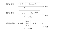
- FIG. 4 is an explanatory diagram showing a time change of a signal when an abnormality has occurred in a first signal source 1;
- FIG. 4 is an explanatory diagram showing a time change of a signal when an abnormality occurs in a second signal source 2.
- FIG. 5 is a configuration diagram illustrating another clock generation device according to the first embodiment.
- FIG. 9 is a configuration diagram illustrating a clock generation device including a phase difference detection circuit 4 according to a second embodiment.
- FIG. 9 is a configuration diagram illustrating a determination circuit 30 of the phase difference detection circuit 4 according to the second embodiment. And abnormality occurs in both the first signal source 1 and the second signal source 2, a first abnormality occurrence time t 1 of the signal source 1 and the abnormality occurrence time t 2 of the second signal source 2
- FIG. 9 is an explanatory diagram showing a time change of a signal in a late case (t 1 ⁇ t 1 + ⁇ A ⁇ t 2 ⁇ t 2 + ⁇ B ).
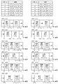
- FIG. 4 is an explanatory diagram showing a time change of a digital signal in patterns (1) to (12).
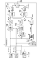
- FIG. 11 is a configuration diagram illustrating a clock generation device including a phase difference detection circuit 6 according to a third embodiment.
- FIG. 14 is a configuration diagram illustrating a determination circuit 49 of the phase difference detection circuit 6 according to the third embodiment.
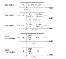
- FIG. 4 is an explanatory diagram showing a time change of a signal when an abnormality has occurred in a first signal source 1;
- FIG. 4 is an explanatory diagram showing a time change of a signal when an abnormality occurs in a second signal source 2.
- FIG. 7 is an explanatory diagram showing a time change of a signal in a case where the signal is late (t 1 ⁇ t 2 ).
- FIG. 13 is a configuration diagram illustrating another clock generation device according to the third embodiment.
- FIG. 1 is a configuration diagram showing a clock generation device including the phase difference detection circuit 4 according to the first embodiment.
- a first signal source 1 is a signal source targeted for abnormality detection, and is realized by a crystal oscillator, a rubidium oscillator, a cesium oscillator, a VCO (Voltage Controlled Oscillator), a DDS, or the like.
- the first signal source 1 outputs a first signal having a frequency f 1 and an initial phase ⁇ 1 to each of the clock signal generator 3, the first frequency converter 11, and the first delay circuit 12. I do.
- the second signal source 2 is a signal source targeted for abnormality detection, and is realized by a crystal oscillator, a rubidium oscillator, a cesium oscillator, a VCO, a DDS, or the like.
- the second signal source 2 outputs a second signal having a frequency of f 2 and an initial phase of ⁇ 2 to each of the clock signal generator 3, the first frequency converter 11, and the second delay circuit 13. I do.
- the clock signal generator 3 is realized by a multiplier or a frequency divider.
- the clock signal generation unit 3 generates a clock signal using the first signal output from the first signal source 1 and the second signal output from the second signal source 2.
- the clock signal generation unit 3 generates one clock signal from the first signal and the second signal.
- the clock signal generator 3 may generate one clock signal from the first signal and generate another clock signal from the second signal.
- the phase difference detection circuit 4 monitors the first signal output from the first signal source 1 and the second signal output from the second signal source 2, and detects the first signal source 1 or the second signal source 2. Of the signal source 2 is detected.
- the phase difference detection circuit 4 monitors the first signal output from the first signal source 1 and the second signal output from the second signal source 2, and Among the second signal sources 2, a signal source having an abnormality is determined.
- the first frequency converter 11 is realized by a mixer, a sample and hold circuit, or a circuit in which a mixer and a sample and hold circuit are combined.
- the first frequency converter 11 generates a third signal from the first signal output from the first signal source 1 and the second signal output from the second signal source 2, and generates a third signal. 3 is output to the first filter 15.
- the first frequency converter 11 generates a third signal by converting the frequency of the first signal using the second signal.
- the first delay circuit 12 is realized by a through line having a fixed line length.
- the first delay circuit 12 may be implemented by a first delay time tau A variable length coaxial tube adjustment is possible.
- First delay circuit 12 a first signal output from the first signal source 1 is delayed by a first delay time tau A, as a fourth signal, the first signal after a delay the second Is output to the frequency converter 14.
- the second delay circuit 13 is realized by a through line having a fixed line length.
- the second delay circuit 13 may be implemented by a second delay time ⁇ variable length coaxial tube adjustment is possible B.
- the second delay circuit 13 a second signal output from the second signal source 2 is delayed by a second delay time tau B, as a fifth signal, the second signal after a delay the second Is output to the frequency converter 14.
- the first delay time ⁇ A in the first delay circuit 12 and the second delay time ⁇ B in the second delay circuit 13 are different delay times. In the first embodiment, an example in which ⁇ A ⁇ B is described, but ⁇ A > ⁇ B may be used.
- the second frequency converter 14 is realized by a mixer, a sample and hold circuit, or a circuit in which a mixer and a sample and hold circuit are combined.
- the second frequency converter 14 generates a sixth signal from the fourth signal output from the first delay circuit 12 and the fifth signal output from the second delay circuit 13, 6 is output to the second filter 16.
- the second frequency converter 14 generates a sixth signal by converting the frequency of the second signal using the fifth signal.
- the frequency of the sixth signal output from the second frequency converter 14 is the same as the frequency of the third signal output from the first frequency converter 11.
- the first frequency converter 11 converts the frequency of the first signal using the second signal, and converts the first signal after the frequency conversion into a first filter 15 as a third signal. Output to However, this is only an example, and the first frequency converter 11 converts the frequency of the second signal using the first signal, and generates the third signal after the frequency conversion as the third signal. May be output to the first filter 15.
- the second frequency converter 14 converts the frequency of the fifth signal using the fourth signal. The frequency is converted, and a fifth signal after frequency conversion is output to the second filter 16 as a sixth signal.
- the first filter 15 is realized by a chip inductor, a chip capacitor, an LPF (Low Pass Filter), a BPF (Band Pass Filter), or the like. Further, the first filter 15 may be realized by a microstrip, a coaxial resonator, or the like.
- the first filter 15 has a pass band through which the signal component of the third signal output from the first frequency converter 11 passes, and is a filter that suppresses signals outside the pass band and unnecessary waves. . Therefore, the first filter 15 suppresses the spurious signal included in the third signal output from the first frequency converter 11, and suppresses the spurious signal in the third signal (hereinafter, “third signal”). (Referred to as “signal”) to the comparator 17.
- the second filter 16 is realized by a chip inductor, a chip capacitor, an LPF, a BPF, or the like. Further, the second filter 16 may be realized by a microstrip, a coaxial resonator, or the like.
- the second filter 16 has a pass band through which the signal component of the sixth signal output from the second frequency converter 14 passes, and is a filter that suppresses signals outside the pass band and unnecessary waves. . Therefore, the second filter 16 suppresses the spurious signal included in the sixth signal output from the second frequency converter 14, and suppresses the spurious signal in the sixth signal (hereinafter, “sixth signal”). (Referred to as “signal of”) to the comparator 17.
- the comparator 17 is realized by a mixer or the like.
- the comparator 17 compares the phase of the third ′ signal output from the first filter 15 with the phase of the sixth ′ signal output from the second filter 16, and compares the phase of the third ′ signal. The phase difference between the phase and the phase of the sixth signal is detected.
- the comparator 17 outputs a seventh signal indicating the detected phase difference to an ADC (Analog to Digital Converter) 18.
- ADC Analog to Digital Converter
- the ADC 18 is an analog-to-digital converter realized by a ⁇ -type AD (Analog to Digital) converter or a flash-type AD converter.
- the ADC 18 converts the seventh signal output from the comparator 17 from an analog signal to a digital signal, and outputs the digital signal to the determination circuit 19.
- the ADC 18 converts the seventh signal from an analog signal to a digital signal by sampling the seventh signal in synchronization with the clock signal, and outputs the digital signal to the determination circuit 19.
- the clock signal may be a clock signal output from the clock signal generation unit 3 or a signal supplied from outside the clock generation device.
- the ADC 18 includes a memory for storing a digital signal every time the seventh signal is converted from an analog signal to a digital signal, averages a plurality of digital signals, and outputs the averaged digital signal to the determination circuit 19. You may.
- the determination circuit 19 is realized by an FPGA (Field Programmable Gate Array) or the like.
- the determination circuit 19 includes a phase calculation unit 21, a change time measurement unit 22, and a determination unit 23 (see FIG. 2).
- the determination circuit 19 detects occurrence of an abnormality in the first signal source 1 or the second signal source 2 based on the digital signal output from the ADC 18. For example, if the phase of the digital signal output from the ADC 18 does not change with the passage of time, the determination circuit 19 has no abnormality in either the first signal source 1 or the second signal source 2. Is determined.
- the determination circuit 19 determines that the first signal source 1 or the second signal source 2 has an abnormality if the phase of the digital signal output from the ADC 18 changes over time. Further, the determination circuit 19 determines which of the first signal source 1 and the second signal source 2 has an abnormality based on the time change of the phase of the digital signal output from the ADC 18. Is determined.
- FIG. 2 is a configuration diagram illustrating the determination circuit 19 of the phase difference detection circuit 4 according to the first embodiment.
- the phase calculator 21 calculates the phase of the digital signal output from the ADC 18 and outputs the calculated phase to the change time measuring unit 22.
- the change time measurement unit 22 detects a change in the phase output from the phase calculation unit 21. Upon detecting the change in the phase, the change time measuring unit 22 measures the time from when the change is detected until the changed phase returns to the original phase, and outputs the measured time to the determination unit 23.
- the determination unit 23 detects occurrence of an abnormality in the first signal source 1 or the second signal source 2 based on the time output from the change time measurement unit 22. For example, if the time output from the change time measurement unit 22 is zero, the determination unit 23 determines a determination result indicating that there is no abnormality in both the first signal source 1 and the second signal source 2. Output. Further, the determination unit 23 determines which of the first signal source 1 and the second signal source 2 has an abnormality based on the time output from the change time measurement unit 22. I do. For example, the determination unit 23, the time output from the change time measuring unit 22 when the first delay time tau A, and outputs a determination result indicating that an abnormality in the first signal source 1 is generated . Determination unit 23, the time output from the change time measuring unit 22 when the second delay time tau B, and outputs a determination result indicating that an abnormality to the second signal source 2 is generated.
- phase difference detection circuit 4 shown in FIG. 1 a through line is used as the first delay circuit 12 and the second delay circuit 13, and the first frequency converter 11, the second frequency converter 14, and the comparator It is assumed that a mixer is used as 17. Also, among the components of the phase difference detection circuit 4 shown in FIG. 1, components other than the first delay circuit 12 and the second delay circuit 13 delay the time from when the signal is input to when the signal is output. Shall not occur.
- the first signal source 1 converts the first signal having the frequency f 1 and the initial phase ⁇ 1 into the clock signal generator 3 and the first frequency converter 11. And the first delay circuit 12.
- t is time, and the same applies to the following expressions.
- the second signal source 2 converts the second signal having the frequency f 2 and the initial phase ⁇ 2 into the clock signal generator 3 and the first frequency converter 11. And the second delay circuit 13.
- f 1 > f 2 for convenience of explanation.
- First delay circuit 12 when the first signal source 1 receives the first signal, delaying the first signal by a first delay time tau A.
- the first delay circuit 12 outputs a fourth signal represented by the following equation (3) to the second frequency converter 14 as a delayed first signal.
- the second delay circuit 13 when the second signal source 2 receives the second signal, delays the second signal by a second delay time tau B.
- the second delay circuit 13 outputs a fifth signal represented by the following equation (4) to the second frequency converter 14 as a delayed second signal.
- the first frequency converter 11 mixes the first signal output from the first signal source 1 and the second signal output from the second signal source 2 and generates a third signal as a third signal.
- a mixed signal of the first signal and the second signal is output to the first filter 15.
- the second frequency converter 14 mixes the fourth signal output from the first delay circuit 12 and the fifth signal output from the second delay circuit 13 and generates a sixth signal as a sixth signal.
- the mixed signal of the fourth signal and the fifth signal is output to the second filter 16.
- the output frequency of the mixer is represented by the following equations (5) and (6). Is done. In Expressions (5) and (6), m and n are positive integers.
- the two signals input to the first frequency converter 11 are a first signal and a second signal.
- the frequency of the first signal is f 1 and the frequency of the second signal is f 2 .
- the two signals input to the second frequency converter 14 are a fourth signal and a fifth signal.
- the frequency of the fourth signal is f 1 and the frequency of the fifth signal is f 2 . is there.
- the desired frequency of the third signal that is the output signal of the first frequency converter 11 is f 1 ⁇ f 2
- the desired frequency of the sixth signal that is the output signal of the second frequency converter 14 is Assume that the desired frequency is f 1 -f 2 .
- the desired frequency of the third signal is defined by the designer of the clock generation device shown in FIG.
- the third signal 1 among the output frequencies of the mixers represented by Expressions (5) and (6), as the third signal. It means the frequency of the output signal.
- the third signal output from the first frequency converter 11 is represented by the following equation (7).
- the first filter 15 When the first filter 15 receives the third signal from the first frequency converter 11, the first filter 15 passes the signal of the frequency f 1 -f 2 among the signals included in the third signal, and The spurious signal included in the signal No. 3 is suppressed.
- the third signal that is, the third signal whose spurious signal is suppressed by the first filter 15, that is, the signal of the frequency f 1 -f 2 is input to the comparator 17.
- the second filter 16 passes the signal of the frequency f 1 -f 2 out of the signals included in the sixth signal, and 6. The spurious signal included in the signal No. 6 is suppressed.
- the first filter 15 and the second filter 16 are provided to prevent a malfunction and a failure of the comparator 17 due to a large number of spurious signals being input to the comparator 17.
- the spurious signal included in the third signal and the spurious signal included in the sixth signal are frequencies other than the frequency at which the comparator 17 can operate, or when the power of the spurious signal is low In this case, the malfunction and failure of the comparator 17 do not occur.
- the first filter 15 and the second filter 16 may not be mounted on the phase difference detection circuit 4.
- the comparator 17 When the comparator 17 receives the third signal from the first filter 15 and receives the sixth signal from the second filter 16, the comparator 17 determines the phase of the third signal and the phase of the sixth signal. And the phase difference between the phase of the 3 ′ signal and the phase of the 6 ′ signal is detected. The comparator 17 outputs a seventh signal indicating the detected phase difference to the ADC 18.
- a mixer is used as the comparator 17, and the output signal of the mixer is generally represented by Expressions (5) and (6).
- the ADC 18 Upon receiving the seventh signal from the comparator 17, the ADC 18 converts the seventh signal from an analog signal to a digital signal, and outputs the digital signal to the determination circuit 19.
- the determination circuit 19 Upon receiving the digital signal from the ADC 18, the determination circuit 19 generates an abnormality in one of the first signal source 1 and the second signal source 2 based on the time change of the phase of the digital signal. Is determined.
- the determination processing by the determination circuit 19 will be specifically described.
- the phase calculation unit 21 calculates the phase of the digital signal, and outputs the calculated phase to the change time measurement unit 22.
- the change time measurement unit 22 detects a change in the phase output from the phase calculation unit 21.
- the change time measuring unit 22 measures the time ⁇ t from the time of detection of the change until the changed phase returns to the original phase, and outputs the measured time ⁇ t to the determination unit 23.
- Determination unit 23 the time ⁇ t which is outputted from the change time measuring unit 22 when the first delay time tau A, abnormality in a first signal source 1 outputs a determination result indicating that has occurred. If the time ⁇ t output from the change time measuring unit 22 is the second delay time ⁇ B , the determining unit 23 outputs a determination result indicating that an abnormality has occurred in the second signal source 2. I do.
- FIG. 3 is an explanatory diagram showing a time change of a signal when an abnormality occurs in the first signal source 1.
- the horizontal axis is time.
- the second signal source 2 is normal shows an example in which abnormality occurs when a first signal source 1 is a time t 1.
- the frequency of the first signal output from the first signal source 1 changes from f 1 to (f 1 + ⁇ f 1 ) because an abnormality has occurred in the first signal source 1. changes, the initial phase is changed to the theta 1 'from theta 1.
- the first signal output from the first signal source 1 is transmitted to the first frequency converter 11 without delay, and the second signal output from the second signal source 2 is output without delay. Transmitted. Then, the spurious signal of the third signal output from the first frequency converter 11 is suppressed by the first filter 15 and transmitted to the comparator 17 as a third 'signal. Therefore, as shown in FIG. 3, the frequency of the third ′ signal changes from f 1 ⁇ f 2 to (f 1 + ⁇ f 1 ) ⁇ f 2 at time t 1 .
- the second frequency converter 14 a first signal output from the first signal source 1 is transmitted delayed by the first delay time tau A, output from the second signal source 2 a second signal is transmitted with a delay of second delay time tau B.
- the spurious signal of the sixth signal output from the second frequency converter 14 is suppressed by the second filter 16 and transmitted to the comparator 17 as the sixth signal. Accordingly, the frequency of the sixth signal changes from f 1 -f 2 to (f 1 + ⁇ f 1 ) -f 2 at time t 1 + ⁇ A as shown in FIG.
- the sixth' third and signals in the initial phases are different by a frequency the same. Therefore, in the time before the time t 1, the digital signal indicating the phase of the seventh signal, i.e., 'a signal, the sixth' third digital signal indicating the phase difference between the phase of the signal, a constant It is. From time t 1 to time t 1 + ⁇ A , the frequency of the third ′ signal is (f 1 + ⁇ f 1 ) ⁇ f 2 and the frequency of the sixth ′ signal is f 1 ⁇ f 2 . Therefore, the phase of the digital signal indicating the phase difference changes over time. The phase of the digital signal changes by a frequency ⁇ f 1 every second.
- the third ′ signal and the sixth ′ signal have the same frequency. Therefore, the phase of the digital signal indicating the phase difference between the third 'signal and the sixth' signal is constant.
- the determination unit 23 if the time ⁇ t output from the change time measuring unit 22 is a first delay time tau A, outputs a determination result indicating that abnormality in a first signal source 1 is generated I do.
- FIG. 4 is an explanatory diagram showing a time change of a signal when an abnormality has occurred in the second signal source 2.
- the horizontal axis is time.
- the first signal source 1 is normal shows an example in which abnormality has occurred when the second signal source 2 is a time t 2.
- the time t 2 subsequent to abnormality in the second signal source 2 is generated, the frequency of the second signal output from the second signal source 2, from f 2 (f 2 + ⁇ f 2 ) changes, the initial phase is changed to the theta 2 'from theta 2.
- the first signal output from the first signal source 1 is transmitted to the first frequency converter 11 without delay, and the second signal output from the second signal source 2 is output without delay. Transmitted. Then, the spurious signal of the third signal output from the first frequency converter 11 is suppressed by the first filter 15 and transmitted to the comparator 17 as a third 'signal. Therefore, the frequency of the signal of the 3 ', as shown in FIG. 4, at time t 2, the from f 1 -f 2 f 1 - varies (f 2 + ⁇ f 2).
- the second frequency converter 14 a first signal output from the first signal source 1 is transmitted delayed by the first delay time tau A, output from the second signal source 2 a second signal is transmitted with a delay of second delay time tau B.
- the spurious signal of the sixth signal output from the second frequency converter 14 is suppressed by the second filter 16 and transmitted to the comparator 17 as the sixth signal. Therefore, the frequency of the signal of the 6 ', as shown in FIG. 4, at time t 2 + tau B, from f 1 -f 2 f 1 - varies (f 2 + ⁇ f 2).
- the sixth' third and signals in the initial phases are different by a frequency the same. Therefore, the time before the time t 2, the digital signal indicating the phase of the seventh signal, i.e., 'a signal, the sixth' third digital signal indicating the phase difference between the phase of the signal, a constant It is.
- the digital signal indicating the phase of the seventh signal i.e., 'a signal
- the sixth' third digital signal indicating the phase difference between the phase of the signal, a constant It is.
- the phase of the digital signal changes by a frequency ⁇ f 2 every second .
- the change time measuring unit 22 the time output from Delta] t, i.e., from the time t 2 that has detected the change in phase, changes The time until time t 2 + ⁇ B when the obtained phase returns to the original phase coincides with the second delay time ⁇ B. Therefore, the determination unit 23, if the time ⁇ t output from the change time measuring section 22 is a second delay time tau B, outputs a determination result indicating that an abnormality to the second signal source 2 is generated I do.
- FIG. 3 shows a time change of the signal when the first signal source 1 has an abnormality
- FIG. The time change is shown.
- the frequency of the 3 ′ signal and the frequency of the 6 ′ signal are constant without change. It is. Therefore, the phase of the digital signal indicating the phase difference between the third 'signal and the sixth' signal does not change over time. Therefore, if the time ⁇ t output from the change time measurement unit 22 is zero, the determination unit 23 determines that there is no abnormality in any of the first signal source 1 and the second signal source 2 Is output.
- the first signal generating the third signal from the first signal output from the first signal source 1 and the second signal output from the second signal source 2
- a frequency converter 11 a first delay circuit 12 for delaying the first signal output from the first signal source 1 and outputting the fourth signal as a fourth signal, and a first delay circuit 12 output from the second signal source 2
- a second delay circuit 13 that delays the second signal and outputs the fifth signal as a fifth signal, a fourth signal output from the first delay circuit 12 and a fifth signal output from the second delay circuit 13.
- a second frequency converter 14 that generates a sixth signal having the same frequency as the frequency of the third signal from the signal, a phase of the third signal generated by the first frequency converter 11, A seventh signal indicating the phase difference from the phase of the sixth signal generated by the second frequency converter 14 is And a comparator 17 for detecting the occurrence of an abnormality in the first signal source 1 or the second signal source 2 based on the seventh signal output from the comparator 17.
- the phase difference detection circuit 4 is configured. Therefore, even if the phase jitter is superimposed, the phase difference detection circuit 4 can prevent erroneous determination of whether there is an abnormality in the signal source.
- the first delay circuit 12 delays the first signal output from the first signal source 1 by a first delay time
- the second delay circuit 13 The second circuit output from the signal source 2 is delayed by a second delay time different from the first delay time
- the determination circuit 19 detects the time change of the phase of the seventh signal output from the comparator 17.
- the phase difference detection circuit 4 is configured to determine which of the first signal source 1 and the second signal source 2 has an abnormality. Therefore, the phase difference detection circuit 4 can specify which signal source has an abnormality.
- the frequency of the two signals input to the first frequency converter 11 and the frequency of the two signals input to the second frequency converter 14 are both: f 1 and f 2 are the same. However, it is sufficient that the frequency of the two signals input to the first frequency converter 11 and the frequency of the two signals input to the second frequency converter 14 are the same.
- the frequency of the two signals input to 14 is not limited to the case where both frequencies are f 1 and f 2 . Therefore, the phase difference detection circuit 4 may include, for example, the following four frequency converters (1) to (4). Each of the four frequency converters (1) to (4) can be realized by a frequency divider or a multiplier.
- Frequency converter (1) the frequency f 1 of the first signal into a frequency f 3, a converter for outputting a signal of a frequency f 3 to the first frequency converter 11.
- Frequency converter (2) the frequency f 2 of the second signal into a frequency f 4, a converter for outputting a signal of a frequency f 4 to the first frequency converter 11.
- Frequency converter (3) the frequency f 1 of the fourth signal into a frequency f 3, a converter for outputting a signal of a frequency f 3 to the second frequency converter 14.
- the frequency of the third signal output from the first filter 15 is converted using a frequency divider or a multiplier, and the frequency of the third signal is converted from the second filter 16 using a frequency divider or a multiplier.
- the frequency of the output sixth signal may be converted.
- the frequency of the third 'signal after the frequency conversion and the frequency of the sixth' signal after the frequency conversion are the same frequency.
- the clock generation device shown in FIG. 1 includes a first signal source 1 and a second signal source 2, and the frequency f1 of the first signal output from the first signal source 1 is equal to the second signal source 2. is high (f 1> f 2) than the frequency f 2 of the second signal output from the signal source 2. However, this is only an example, and the frequency f1 of the first signal output from the first signal source 1 is equal to or lower than the frequency f2 of the second signal output from the second signal source 2 (f 1 ⁇ f 2 ).
- each of the desired frequency of the third signal and sixth signal may be a f 1 + f 2.
- the phase difference detection circuit 4 shown in FIG. 1 includes an ADC 18 that converts the seventh signal output from the comparator 17 from an analog signal to a digital signal, and outputs the digital signal to the determination circuit 19.
- the phase difference detection circuit 4 may include the following two ADCs (1) and (2) instead of the ADC 18.
- the ADC (1) is an ADC that converts the third signal output from the first filter 15 from an analog signal to a digital signal, and outputs the digital signal to the comparator 17.
- the ADC (2) is an ADC that converts the sixth signal output from the second filter 16 from an analog signal to a digital signal, and outputs the digital signal to the comparator 17.
- the clock generator shown in FIG. 1 may implement a measurement circuit for measuring the power or current of the first signal. It may be. Judging circuit 19, when the power of the first signal measured by the measuring circuit is smaller than the threshold value Th 1, or a current of the first signal is less than the threshold value Th 2, the first signal source 1 Detect failure. Further, in order to be able to detect a failure in which the second signal source 2 does not output the second signal, the clock generation device shown in FIG.
- the thresholds Th 1 and Th 2 may be stored in an internal memory of the determination circuit 19 or may be externally provided.
- each of the first delay circuit 12 and the second delay circuit 13 is a through line.
- each of the first delay circuit 12 and the second delay circuit 13 may be a filter.
- the filter has a time constant, if each of the first delay circuit 12 and the second delay circuit 13 is a filter, the abnormality of the first signal source 1 or the second signal source 2 The change in the output signal of the filter due to the occurrence lags behind the change in the input signal of the filter.
- the clock generation device shown in FIG. 1 similarly generates an abnormality in any signal source even when the phase of the 3 ′ signal and the phase of the 6 ′ signal change with the occurrence of the abnormality. Can be specified.
- the determination circuit 19 determines which one of the first signal source 1 and the second signal source 2 is based on the time ⁇ t output from the change time measurement unit 22. It is determined whether an error has occurred. Only when the phase change amount calculated by the phase calculation unit 21 is equal to or greater than the threshold value, the determination circuit 19 generates an abnormality in any signal source based on the time ⁇ t output from the change time measurement unit 22. May be determined.
- the threshold value may be stored in an internal memory of the determination circuit 19 or may be externally provided.
- the clock generation device shown in FIG. 1 includes a first signal source 1 and a second signal source 2, and the determination circuit 19 determines which one of the first signal source 1 and the second signal source 2 It is determined whether an abnormality has occurred in the signal source.
- this is only an example, and a clock generation device including the third signal source 5 in addition to the first signal source 1 and the second signal source 2 may be used.
- FIG. 5 is a configuration diagram showing another clock generation device according to the first embodiment. 5, the same reference numerals as those in FIG. 1 denote the same or corresponding parts, and a description thereof will not be repeated.
- the third signal source 5 is a signal source targeted for abnormality detection, and is realized by a crystal oscillator, a rubidium oscillator, a cesium oscillator, a VCO, a DDS, or the like.
- the third signal source 5 outputs a signal having a frequency of f 3 and an initial phase of ⁇ 3 to the clock signal generator 3, the first frequency converter 11 of the phase difference detection circuit 4a, and the first signal of the phase difference detection circuit 4a.
- the output is provided to each of the two delay circuits 13.
- the first signal source 1 outputs the first signal to the clock signal generation unit 3, the first frequency converter 11 of the phase difference detection circuit 4, and the second signal of the phase difference detection circuit 4. To each of the delay circuits 13. Further, the first signal source 1 outputs the signals to the first frequency converter 11 of the phase difference detection circuit 4a and the second delay circuit 13 of the phase difference detection circuit 4a, respectively.
- the phase difference detection circuit 4 a has the same configuration as the phase difference detection circuit 4, and receives the first signal output from the first signal source 1 and the signal output from the third signal source 5. I do.
- the determination circuit 19 of the phase difference detection circuit 4a determines which of the first signal source 1 and the third signal source 5 has an abnormality.
- the clock signal generator 3a is realized by a multiplier or a frequency divider.
- the clock signal generation unit 3a uses the first signal output from the first signal source 1, the second signal output from the second signal source 2, and the signal output from the third signal source 5. To generate a clock signal.
- the clock signal generation unit 3a generates one clock signal from the first signal, the second signal, and the signal output from the third signal source 5.
- the clock signal generator 3 generates one clock signal from the first signal, generates one clock signal from the second signal, and outputs the clock signal from the third signal source 5.
- One clock signal may be generated from the obtained signal.
- the clock generation device shown in FIG. 5 can determine which of the first signal source 1, the second signal source 2, and the third signal source 5 has an abnormality.
- the clock generation device shown in FIG. 1 includes two signal sources, and the clock generation device illustrated in FIG. 5 includes three signal sources. However, these are merely examples, and a clock generation device including N (N is an integer of 4 or more) signal sources may be used.
- Each of the phase difference detection circuits 4n is a circuit having the same configuration as the phase difference detection circuit 4, and receives the first signal output from the first signal source 1 and the signal output from the (n + 1) th signal source. .
- the determination circuit 19 of the phase difference detection circuit 4n determines which of the first signal source 1 and the (n + 1) th signal source has an abnormality.
- Embodiment 2 FIG.
- the determination circuit 19 determines which one of the first signal source 1 and the second signal source 2 based on the time change of the phase of the digital signal output from the ADC 18. To determine if the source is abnormal.
- the determination circuit 19 not only determines which signal source has an abnormality, but also determines whether an abnormality has occurred in both the first signal source 1 and the second signal source 2. A clock generation device that can judge is described.
- FIG. 6 is a configuration diagram illustrating a clock generation device including the phase difference detection circuit 4 according to the second embodiment. 6, the same reference numerals as those in FIG. 1 denote the same or corresponding parts, and a description thereof will be omitted.
- the determination circuit 30 is realized by an FPGA or the like.
- the determination circuit 30 includes a phase calculation unit 21, a change time measurement unit 22, and a determination unit 31.
- the determination circuit 30 detects occurrence of an abnormality in the first signal source 1 or the second signal source 2 based on the digital signal output from the ADC 18.
- the determination circuit 30 determines which of the first signal source 1 and the second signal source 2 has an abnormality based on the time change of the phase of the digital signal output from the ADC 18. And a circuit that determines whether an abnormality has occurred in both signal sources.
- FIG. 7 is a configuration diagram illustrating the determination circuit 30 of the phase difference detection circuit 4 according to the second embodiment.
- the determination unit 31 counts the number of times of the time measurement by the change time measurement unit 22, and the change in the phase change amount calculated by the phase calculation unit 21 while the time is measured by the change time measurement unit 22. It is determined whether or not there is. If the number of measurements is one, the amount of change does not change, and the time output from the change time measuring unit 22 is the first delay time ⁇ A , the determination unit 31 determines that the first signal source 1 A determination result indicating that an error has occurred is output.
- the determination unit 31 A determination result indicating that an error has occurred is output. If the number of times of measurement is two, the determination unit 31 outputs a determination result indicating that both the first signal source 1 and the second signal source 2 have an abnormality. In addition, if the number of times of measurement is one and the amount of change is changed, the determination unit 31 reports that both the first signal source 1 and the second signal source 2 are abnormal. Output the judgment result shown. If the number of measurements is 0, the determination unit 31 outputs a determination result indicating that there is no abnormality in both the first signal source 1 and the second signal source 2.
- the operation of the phase difference detection circuit 4 shown in FIG. 6 will be described. However, since the configuration other than the determination circuit 30 is the same as that of the phase difference detection circuit 4 shown in FIG. 1, only the operation of the determination circuit 30 will be described here.
- the time change of the signal is as shown in FIG. Is represented by In Figure 3, the second signal source 2 is normal shows an example in which abnormality occurs when a first signal source 1 is a time t 1.
- the time before the time t 1 since the first signal source 1 is normal, the frequency of the first signal output from the first signal source 1 is f 1.
- the frequency of the first signal output from the first signal source 1 changes from f 1 to (f 1 + ⁇ f 1 ) because an abnormality has occurred in the first signal source 1. changes, the initial phase is changed to the theta 1 'from theta 1.
- the first signal output from the first signal source 1 is transmitted to the first frequency converter 11 without delay, and the second signal output from the second signal source 2 is output without delay. Transmitted. Then, the spurious signal of the third signal output from the first frequency converter 11 is suppressed by the first filter 15 and transmitted to the comparator 17 as a third 'signal. Therefore, as shown in FIG. 3, the frequency of the third ′ signal changes from f 1 ⁇ f 2 to (f 1 + ⁇ f 1 ) ⁇ f 2 at time t 1 .
- the second frequency converter 14 a first signal output from the first signal source 1 is transmitted delayed by the first delay time tau A, output from the second signal source 2 a second signal is transmitted with a delay of second delay time tau B.
- the spurious signal of the sixth signal output from the second frequency converter 14 is suppressed by the second filter 16 and transmitted to the comparator 17 as the sixth signal. Accordingly, the frequency of the sixth signal changes from f 1 -f 2 to (f 1 + ⁇ f 1 ) -f 2 at time t 1 + ⁇ A as shown in FIG.
- the sixth' third and signals in the initial phases are different by a frequency the same. Therefore, in the time before the time t 1, the digital signal indicating the phase of the seventh signal, i.e., 'a signal, the sixth' third digital signal indicating the phase difference between the phase of the signal, a constant It is. From time t 1 to time t 1 + ⁇ A , the frequency of the third ′ signal is (f 1 + ⁇ f 1 ) ⁇ f 2 and the frequency of the sixth ′ signal is f 1 ⁇ f 2 . Therefore, the phase of the digital signal indicating the phase difference changes over time.
- the phase of the digital signal changes by a frequency ⁇ f 1 every second, and the amount of change in the phase of the digital signal is constant. Therefore, there is no change in the amount of change during the time when the change time measuring unit 22 is measuring the time.
- the third ′ signal and the sixth ′ signal have the same frequency. Therefore, the phase of the digital signal indicating the phase difference between the third 'signal and the sixth' signal is constant.
- the determination unit 31 determines that the number of times of the time measurement by the change time measurement unit 22 is one, the change amount does not change, and the time output from the change time measurement unit 22 is the first delay time ⁇ A If so, a determination result indicating that an abnormality has occurred in the first signal source 1 is output.
- the time change of the signal when only the second signal source 2 has an abnormality among the first signal source 1 and the second signal source 2 is as shown in FIG. Is represented by In Figure 4, the first signal source 1 is normal shows an example in which abnormality has occurred when the second signal source 2 is a time t 2.
- the time t 2 subsequent to abnormality in the second signal source 2 is generated, the frequency of the second signal output from the second signal source 2, from f 2 (f 2 + ⁇ f 2 ) changes, the initial phase is changed to the theta 2 'from theta 2.
- the first signal output from the first signal source 1 is transmitted to the first frequency converter 11 without delay, and the second signal output from the second signal source 2 is output without delay. Transmitted. Then, the spurious signal of the third signal output from the first frequency converter 11 is suppressed by the first filter 15 and transmitted to the comparator 17 as a third 'signal. Therefore, the frequency of the signal of the 3 ', as shown in FIG. 4, at time t 2, the from f 1 -f 2 f 1 - varies (f 2 + ⁇ f 2).
- the second frequency converter 14 a first signal output from the first signal source 1 is transmitted delayed by the first delay time tau A, output from the second signal source 2 a second signal is transmitted with a delay of second delay time tau B.
- the spurious signal of the sixth signal output from the second frequency converter 14 is suppressed by the second filter 16 and transmitted to the comparator 17 as the sixth signal. Therefore, the frequency of the signal of the 6 ', as shown in FIG. 4, at time t 2 + tau B, from f 1 -f 2 f 1 - varies (f 2 + ⁇ f 2).
- the sixth' third and signals in the initial phases are different by a frequency the same. Therefore, the time before the time t 2, the digital signal indicating the phase of the seventh signal, i.e., 'a signal, the sixth' third digital signal indicating the phase difference between the phase of the signal, a constant It is. Time t 2 later in time until t 2 + tau B, third 'frequency signal of f 1 - is (f 2 + ⁇ f 2), the sixth' frequency of the signal is at f 1 -f 2 Therefore, the phase of the digital signal indicating the phase difference changes over time.
- the phase of the digital signal changes by a frequency ⁇ f 2 every second, and the amount of change in the phase of the digital signal is constant. Therefore, there is no change in the amount of change during the time when the change time measuring unit 22 is measuring the time.
- the sixth' third signal of the frequency is the same. Therefore, the phase of the digital signal indicating the phase difference between the third 'signal and the sixth' signal is constant.
- the change time measuring unit 22 determines that the number of times of time measurement by the change time measurement unit 22 is one, the change amount does not change, and the time output from the change time measurement unit 22 is the second delay time ⁇ B If so, a determination result indicating that an abnormality has occurred in the second signal source 2 is output.
- the frequency of the first signal output from the first signal source 1 is f 1 It is.
- the frequency of the first signal output from the first signal source 1 changes from f 1 to (f 1 + ⁇ f 1) changes, the initial phase is changed to the theta 1 'from theta 1.
- the frequency of the second signal output from the second signal source 2 changes from f 2 to (f 2 + ⁇ f 2) changes, the initial phase is changed to the theta 2 'from theta 2.
- the first signal output from the first signal source 1 is transmitted to the first frequency converter 11 without delay, and the second signal output from the second signal source 2 is output without delay. Transmitted. Then, the spurious signal of the third signal output from the first frequency converter 11 is suppressed by the first filter 15 and transmitted to the comparator 17 as a third 'signal. Therefore, as shown in FIG. 8, the frequency of the third signal changes from f 1 ⁇ f 2 to (f 1 + ⁇ f 1 ) ⁇ (f 2 + ⁇ f 2 ) at time t 1 .
- the second frequency converter 14 a first signal output from the first signal source 1 is transmitted delayed by the first delay time tau A, output from the second signal source 2 a second signal is transmitted with a delay of second delay time tau B. Then, the spurious signal of the sixth signal output from the second frequency converter 14 is suppressed by the second filter 16 and transmitted to the comparator 17 as the sixth signal. Accordingly, the frequency of the sixth signal changes from f 1 -f 2 to (f 1 + ⁇ f 1 ) -f 2 at time t 1 + ⁇ A as shown in FIG.
- the frequency of the signal of the 6 ' at time t 1 + ⁇ B, (f 1 + ⁇ f 1) from -f 2 (f 1 + ⁇ f 1 ) - change in (f 2 + ⁇ f 2) I do.
- the frequency of the third ′ signal is (f 1 + ⁇ f 1 ) ⁇ (f 2 + ⁇ f 2 ), and the frequency of the sixth signal is ( Since f 1 + ⁇ f 1 ) ⁇ f 2 , the phase of the digital signal indicating the phase difference changes over time.
- the phase of the digital signal changes by a frequency ⁇ f 2 every second, and the amount of change in the phase of the digital signal is constant. Therefore, in the time from time t 1 to time t 1 + ⁇ B , the change amount of the phase difference changes once at time t 1 + ⁇ A , and the time is being measured by the change time measuring unit 22.
- the determination unit 31 sends the signal to both the first signal source 1 and the second signal source 2. A determination result indicating that an abnormality has occurred is output.
- FIG. 9 shows that an abnormality has occurred in both the first signal source 1 and the second signal source 2, and the abnormality of the second signal source 2 has occurred since the abnormality occurrence time t 1 of the first signal source 1.
- time t 2 is an explanatory view showing a time variation of slow when (t 1 ⁇ t 1 + ⁇ a ⁇ t 2 ⁇ t 2 + ⁇ B) of the signal.
- the frequency of the first signal output from the first signal source 1 is f 1.
- the frequency of the first signal output from the first signal source 1 changes from f 1 to (f 1 + ⁇ f 1 ) because an abnormality has occurred in the first signal source 1. changes, the initial phase is changed to the theta 1 'from theta 1.
- the frequency of the second signal output from the second signal source 2 is f 2 at a time before the time t 2 because the second signal source 2 is normal.
- the time t 2 subsequent to abnormality in the second signal source 2 is generated, the frequency of the second signal output from the second signal source 2, from f 2 (f 2 + ⁇ f 2 ) changes, the initial phase is changed to the theta 2 'from theta 2.
- the first signal output from the first signal source 1 is transmitted to the first frequency converter 11 without delay, and the second signal output from the second signal source 2 is output without delay. Transmitted. Then, the spurious signal of the third signal output from the first frequency converter 11 is suppressed by the first filter 15 and transmitted to the comparator 17 as a third 'signal. Therefore, the frequency of the third signal changes from f 1 -f 2 to (f 1 + ⁇ f 1 ) -f 2 at time t 1 as shown in FIG. The frequency of the signal of the 3 ', as shown in FIG. 9, at time t 2, (f 1 + ⁇ f 1) from -f 2 (f 1 + ⁇ f 1 ) - changes to (f 2 + ⁇ f 2).
- the second frequency converter 14 a first signal output from the first signal source 1 is transmitted delayed by the first delay time tau A, output from the second signal source 2 a second signal is transmitted with a delay of second delay time tau B. Then, the spurious signal of the sixth signal output from the second frequency converter 14 is suppressed by the second filter 16 and transmitted to the comparator 17 as the sixth signal. Accordingly, the frequency of the sixth signal changes from f 1 -f 2 to (f 1 + ⁇ f 1 ) -f 2 at time t 1 + ⁇ A as shown in FIG.
- the frequency of the signal of the 6 ' as shown in FIG. 9, at time t 2 + ⁇ B, (f 1 + ⁇ f 1) from -f 2 (f 1 + ⁇ f 1 ) - change in (f 2 + ⁇ f 2) I do.
- the phase of the digital signal indicating the phase difference between the third 'signal and the sixth' signal is constant.
- the frequency of the third ′ signal is (f 1 + ⁇ f 1 ) ⁇ f 2 and the frequency of the sixth ′ signal is f 1 ⁇ f 2 . Therefore, the phase of the digital signal indicating the phase difference changes over time.
- the phase of the digital signal changes by a frequency ⁇ f 1 every second, and the amount of change in the phase of the digital signal is constant.
- the third ′ signal and the sixth ′ signal have the same frequency. Therefore, the phase of the digital signal indicating the phase difference between the third 'signal and the sixth' signal is constant.
- Change time measuring unit 22 is configured to measure the time from time t 1 to time t 1 + tau A, which measures the time from time t 2 to time t 2 + tau B, time is measured twice in total ing. Therefore, if the number of times of measurement is two, the determination unit 31 outputs a determination result indicating that both the first signal source 1 and the second signal source 2 are abnormal.
- FIGS. 8 and 9 show an example of a time change of a signal when both the first signal source 1 and the second signal source 2 have an abnormality.
- Pattern of temporal changes of the digital signals as shown in FIG. 10, an abnormality occurrence time t 1 of the first signal source 1, an abnormality occurrence time t 2 of the second signal source 2, a first delay time ⁇ Twelve patterns (1) to (12) can be classified according to the magnitude relationship between A and the second delay time ⁇ B.
- FIG. 10 is an explanatory diagram showing a time change of the digital signal in the patterns (1) to (12).
- the pattern (1) and the pattern (7) are patterns in which the number of times of time measurement by the change time measurement unit 22 is two. In patterns (2) to (6) and patterns (8) to (12), the number of times of time measurement by the change time measurement unit 22 is one, and the time is being measured by the change time measurement unit 22. In this pattern, there is a change in the amount of change in the phase of the digital signal.
- pattern (4) at time t 2, the amount of change in the phase of the digital signal has changed, the pattern (5), at time t 2 and time t 2 + tau B, the amount of change in the phase of the digital signal changes are doing.
- pattern (6) the amount of change in the phase of the digital signal changes at time t 2 + ⁇ B
- pattern (9) the amount of change in the phase of the digital signal changes at time t 1 and time t 2 + ⁇ B
- pattern (10) the amount of change in the phase of the digital signal changes at time t 1 are doing.
- pattern (12) the amount of change in the phase of the digital signal changes at the time t 1 and the time t 1 + ⁇ A
- the amount of change in the phase of the digital signal at the time t 1 + ⁇ A Is changing.
- the determination unit 31 counts the number of times the time is measured by the change time measurement unit 22, and the phase calculation unit It is determined whether or not there is a change in the amount of change in the phase calculated by 21. If the number of measurements is one, the amount of change does not change, and the time measured by the change time measuring unit 22 is the first delay time ⁇ A , the determination unit 31 determines that the first signal source 1 A determination result indicating that an error has occurred is output. If the number of times of measurement is one, the amount of change does not change, and the time measured by the change time measuring unit 22 is the second delay time ⁇ B , the determination unit 31 determines that the second signal source 2 A determination result indicating that an error has occurred is output.
- the determination unit 31 If the number of times of measurement is two, the determination unit 31 outputs a determination result indicating that both the first signal source 1 and the second signal source 2 have an abnormality. In addition, if the number of times of measurement is one and the amount of change is changed, the determination unit 31 reports that both the first signal source 1 and the second signal source 2 are abnormal. Output the judgment result shown. Therefore, the phase difference detection circuit 4 according to the second embodiment is provided not only for the occurrence of an abnormality in the first signal source 1 or the second signal source 2 but also for both the first signal source 1 and the second signal source 2. It can be determined that an abnormality has occurred.
- Embodiment 3 In the clock generation device according to the first embodiment, the first delay time ⁇ A in the first delay circuit 12 and the second delay time ⁇ B in the second delay circuit 13 are different delay times. That is, ⁇ A > ⁇ B or ⁇ A ⁇ B.
- the determination unit 23 determines whether the first signal source 1 and the second signal It cannot be determined which of the sources 2 has an abnormality.
- the first signal source 1 and the second signal A clock generation device that can determine which of the sources 2 has an abnormality will be described.
- FIG. 11 is a configuration diagram illustrating a clock generation device including the phase difference detection circuit 6 according to the third embodiment.
- the phase difference detection circuit 6 monitors the first signal output from the first signal source 1 and the second signal output from the second signal source 2, and monitors the first signal source 1 or the second signal source 2. Of the signal source 2 is detected.
- the phase difference detection circuit 6 monitors the first signal output from the first signal source 1 and the second signal output from the second signal source 2, and Among the second signal sources 2, a signal source in which an abnormality has occurred is determined. Further, the phase difference detection circuit 6 determines whether both the first signal source 1 and the second signal source 2 are abnormal.
- the second frequency converter 41 is realized by a mixer, a sample and hold circuit, or a circuit in which a mixer and a sample and hold circuit are combined.
- the second frequency converter 41 generates a sixth signal from the second signal output from the second signal source 2 and the fourth signal output from the first delay circuit 12, and generates a sixth signal. 6 is output to the second filter 43.
- the second frequency converter 41 converts the frequency of the fourth signal using the second signal, and outputs the fourth signal after the frequency conversion to the second filter 43 as the sixth signal. Output.
- the frequency of the sixth signal output from the second frequency converter 41 is the same as the frequency of the third signal output from the first frequency converter 11.
- the second frequency converter 41 converts the frequency of the fourth signal using the second signal, and converts the fourth signal after the frequency conversion into a second filter 43 as a sixth signal.
- the first frequency converter 11 converts the frequency of the second signal using the first signal
- the second frequency converter 41 uses the fourth signal to convert the frequency of the second signal.
- the frequency of the second signal is converted, and the frequency-converted second signal is output to the second filter 43 as a sixth signal.
- the third frequency converter 42 is realized by a mixer, a sample and hold circuit, or a circuit in which a mixer and a sample and hold circuit are combined.
- the third frequency converter 42 generates a seventh signal from the first signal output from the first signal source 1 and the fifth signal output from the second delay circuit 13, 7 is output to the third filter 44.
- the third frequency converter 42 converts the frequency of the first signal using the fifth signal, and outputs the first signal after the frequency conversion to the third filter 44 as the seventh signal.
- the frequency of the seventh signal output from the third frequency converter 42 is the same as the frequency of the third signal output from the first frequency converter 11.
- the third frequency converter 42 converts the frequency of the first signal using the fifth signal, and converts the first signal after the frequency conversion into a third filter 44 as a seventh signal.
- the third frequency converter 42 uses the first signal to convert the frequency of the second signal.
- the frequency of the fifth signal is converted, and the frequency-converted fifth signal is output to the third filter 44 as a seventh signal.
- the second filter 43 is realized by a chip inductor, a chip capacitor, an LPF, a BPF, or the like. Further, the second filter 43 may be realized by a microstrip, a coaxial resonator, or the like.
- the second filter 43 has a pass band through which the signal component of the sixth signal output from the second frequency converter 41 passes, and is a filter that suppresses signals outside the pass band and unnecessary waves. . Therefore, the second filter 43 suppresses the spurious signal included in the sixth signal output from the second frequency converter 41, and suppresses the spurious signal in the sixth signal (hereinafter, “sixth signal”). (Referred to as “signal”) to the first comparator 45.
- the third filter 44 is realized by a chip inductor, a chip capacitor, an LPF, a BPF, or the like. Further, the third filter 44 may be realized by a microstrip, a coaxial resonator, or the like.
- the third filter 44 has a pass band through which the signal component of the seventh signal output from the third frequency converter 42 passes, and is a filter that suppresses signals outside the pass band and unnecessary waves. . Therefore, the third filter 44 suppresses the spurious signal included in the seventh signal output from the third frequency converter 42, and suppresses the spurious signal in the seventh signal (hereinafter, “seventh signal”). (Referred to as “signal of”) to the second comparator 46.
- the first comparator 45 is realized by a mixer or the like.
- the first comparator 45 compares the phase of the third ′ signal output from the first filter 15 with the phase of the sixth ′ signal output from the second filter 43, and And the phase difference between the phase of the sixth signal and the phase of the sixth signal are detected.
- the first comparator 45 outputs an eighth signal indicating the detected phase difference to the ADC 47.
- the second comparator 46 is realized by a mixer or the like.
- the second comparator 46 compares the phase of the third signal output from the first filter 15 with the phase of the seventh signal output from the third filter 44, and And the phase difference of the 7th signal are detected.
- the second comparator 46 outputs a ninth signal indicating the detected phase difference to the ADC 48.
- the ADC 47 is an analog-to-digital converter realized by a ⁇ AD converter, a flash AD converter, or the like.
- the ADC 47 converts the eighth signal output from the first comparator 45 from an analog signal to a digital signal (hereinafter, referred to as a “first digital signal”), and sends the first digital signal to the determination circuit 49.
- the ADC 47 converts the eighth signal from an analog signal to a first digital signal by sampling the eighth signal in synchronization with the clock signal, and sends the first digital signal to the determination circuit 49.
- the clock signal may be a clock signal output from the clock signal generation unit 3 or a signal supplied from outside the clock generation device.
- the ADC 48 is an analog-to-digital converter realized by a ⁇ AD converter, a flash AD converter, or the like.
- the ADC 48 converts the ninth signal output from the second comparator 46 from an analog signal to a digital signal (hereinafter, referred to as “second digital signal”), and sends the second digital signal to the determination circuit 49.
- second digital signal a digital signal
- the ADC 48 converts the ninth signal from an analog signal to a second digital signal by sampling the ninth signal in synchronization with the clock signal, and sends the second digital signal to the determination circuit 49.
- the clock signal may be a clock signal output from the clock signal generation unit 3 or a signal supplied from outside the clock generation device.
- the ADC 47 includes a memory for storing the first digital signal every time the eighth signal is converted from an analog signal to a first digital signal, and averages the plurality of first digital signals. May be output to the determination circuit 49.
- the ADC 48 includes a memory for storing the second digital signal, and averages the plurality of second digital signals. May be output to the determination circuit 49.
- the determination circuit 49 is realized by an FPGA or the like.
- the determination circuit 49 includes a first phase calculation unit 51, a second phase calculation unit 52, a first change time measurement unit 53, a second change time measurement unit 54, and a determination unit 55 (see FIG. 12). ing.
- the determination circuit 49 determines whether an abnormality has occurred in the first signal source 1 or the second signal source 2 based on each of the first digital signal output from the ADC 47 and the second digital signal output from the ADC 48. To detect.
- the determination circuit 49 also determines the first signal source 1 based on the time change of the phase of the first digital signal output from the ADC 47 and the time change of the phase of the second digital signal output from the ADC 48. Then, it is determined which of the two signal sources 2 has an abnormality. Further, the determination circuit 49 provides both the first signal source 1 and the second signal source 2 based on the time change of the phase of the first digital signal and the time change of the phase of the second digital signal. Determine whether an error has occurred.
- FIG. 12 is a configuration diagram showing the determination circuit 49 of the phase difference detection circuit 6 according to the third embodiment.
- a first phase calculation unit 51 calculates the phase of the first digital signal output from the ADC 47, and outputs the calculated phase to the first change time measurement unit 53.
- the second phase calculation unit 52 calculates the phase of the second digital signal output from the ADC 48 and outputs the calculated phase to the second change time measurement unit 54.
- the first change time measurement unit 53 detects a change in the phase output from the first phase calculation unit 51. When detecting the change in the phase, the first change time measuring unit 53 measures the time from when the change is detected to when the changed phase returns to the original phase, and outputs the measured time to the determination unit 55.
- the second change time measurement unit 54 detects a change in the phase output from the second phase calculation unit 52. When detecting the change in the phase, the second change time measuring unit 54 measures the time from when the change is detected to when the changed phase returns to the original phase, and outputs the measured time to the determination unit 55.
- the determination unit 55 determines whether the first signal source 1 or the second signal source is based on the time output from the first change time measurement unit 53 and the time output from the second change time measurement unit 54, respectively. 2 is detected. In addition, the determination unit 55 determines the first signal source 1 and the second signal source based on the time output from the first change time measurement unit 53 and the time output from the second change time measurement unit 54, respectively. It is determined which of the signal sources 2 has an abnormality. Further, the determination unit 55 provides both the first signal source 1 and the second signal source 2 based on the time change of the phase of the first digital signal and the time change of the phase of the second digital signal. Determine whether an error has occurred.
- phase difference detection circuit 6 shown in FIG. 11 a through line is used as the first delay circuit 12 and the second delay circuit 13, and the first frequency converter 11, the second frequency converter 41, and the third It is assumed that a mixer is used as the frequency converter 42 of FIG. In the phase difference detection circuit 6 shown in FIG. 11, a mixer is used as the first comparator 45 and the second comparator 46. Also, among the components of the phase difference detection circuit 6 shown in FIG. Shall not occur.
- the first signal source 1 converts the first signal shown in the above equation (1) into the clock signal generator 3, the first frequency converter 11, the first delay circuit 12, and the third frequency converter 42. Output to each.
- the second signal source 2 converts the second signal shown in the above equation (2) into the clock signal generator 3, the first frequency converter 11, the second delay circuit 13, and the second frequency converter 41. Output to each.
- First delay circuit 12 when the first signal source 1 receives the first signal, delaying the first signal by a first delay time tau A.
- the first delay circuit 12 outputs the fourth signal shown in the above equation (3) to the second frequency converter 41 as a delayed first signal.
- the second delay circuit 13 when the second signal source 2 receives the second signal, delays the second signal by a second delay time tau B.
- the second delay circuit 13 outputs the fifth signal represented by the above equation (4) to the third frequency converter 42 as a delayed second signal.
- the first frequency converter 11 generates a third signal from the first signal output from the first signal source 1 and the second signal output from the second signal source 2, and generates a third signal. 3 is output to the first filter 15.
- the second frequency converter 41 generates a sixth signal from the second signal output from the second signal source 2 and the fourth signal output from the first delay circuit 12, and generates a sixth signal. 6 is output to the second filter 43.
- the third frequency converter 42 generates a seventh signal from the first signal output from the first signal source 1 and the fifth signal output from the second delay circuit 13, 7 is output to the third filter 44.
- the output frequency of the mixer is represented by the above equations (5) and (6). Is done.
- the two signals input to the first frequency converter 11 are a first signal and a second signal.
- the frequency of the first signal is f 1 and the frequency of the second signal is f 2 .
- the two signals input to the second frequency converter 41 are a second signal and a fourth signal, and the frequency of the second signal is f 2 and the frequency of the fourth signal is f 1 . is there.
- the two signals input to the third frequency converter 42 are a first signal and a fifth signal.
- the frequency of the first signal is f 1 and the frequency of the fifth signal is f 2 . is there.
- the desired frequency of the third signal that is the output signal of the first frequency converter 11 is f 1 ⁇ f 2
- the third signal output from the first frequency converter 11 is represented by the above equation (7).
- the sixth signal output from the second frequency converter 41 is represented by the following equation (9).
- the first filter 15 Upon receiving the third signal from the first frequency converter 11, the first filter 15 suppresses a spurious signal included in the third signal.
- the third signal which is the third signal whose spurious signal has been suppressed by the first filter 15, is input to each of the first comparator 45 and the second comparator 46.
- the second filter 43 When receiving the sixth signal from the second frequency converter 41, the second filter 43 suppresses a spurious signal included in the sixth signal.
- a sixth signal which is a sixth signal whose spurious signal has been suppressed by the second filter 43, is input to the first comparator 45.
- the third filter 44 When receiving the seventh signal from the third frequency converter 42, the third filter 44 suppresses a spurious signal included in the seventh signal.
- the seventh signal which is the seventh signal whose spurious signal has been suppressed by the third filter 44, is input to the second comparator 46.
- the first filter 15, the second filter 43, and the third filter 44 include a first comparator 45 associated with a large number of spurious signals input to the first comparator 45 and the second comparator 46. And the second comparator 46 to prevent malfunction and failure.
- the spurious signal included in each of the third signal, the sixth signal, and the seventh signal is a frequency other than the frequency at which the first comparator 45 and the second comparator 46 can operate, Alternatively, when the power of the spurious signal is low, malfunction and failure do not occur. If no malfunction or failure occurs, the first filter 15, the second filter 43, and the third filter 44 may not be mounted on the phase difference detection circuit 6.
- the first comparator 45 When the first comparator 45 receives the third signal from the first filter 15 and receives the sixth signal from the second filter 43, the phase of the third signal and the sixth signal To detect the phase difference between the phase of the 3 ′ signal and the phase of the 6 ′ signal.
- the first comparator 45 outputs an eighth signal indicating the detected phase difference to the ADC 47.
- a mixer is used as the first comparator 45.
- the output signal of the mixer is represented by Expressions (5) and (6).
- the second comparator 46 When the second comparator 46 receives the third signal from the first filter 15 and receives the seventh signal from the third filter 44, the second comparator 46 receives the phase of the third signal and the seventh signal. And the phase difference between the phase of the third signal and the phase of the seventh signal is detected. The second comparator 46 outputs a ninth signal indicating the detected phase difference to the ADC 48.
- a mixer In the first embodiment, it is assumed that a mixer is used as the second comparator 46. Generally, an output signal of the mixer is represented by Expressions (5) and (6).
- the ADC 47 Upon receiving the eighth signal from the first comparator 45, the ADC 47 converts the eighth signal from an analog signal to a first digital signal, and outputs the first digital signal to the determination circuit 49.
- the ADC 48 Upon receiving the ninth signal from the second comparator 46, the ADC 48 converts the ninth signal from an analog signal to a second digital signal, and outputs the second digital signal to the determination circuit 49.
- the determination circuit 49 Upon receiving the first digital signal from the ADC 47 and receiving the second digital signal from the ADC 48, the determination circuit 49 monitors the time change of the phase of the first digital signal and the time change of the phase of the second digital signal. . The determination circuit 49 determines occurrence of an abnormality in the first signal source 1 or the second signal source 2 based on each of the time change of the phase of the first digital signal and the time change of the phase of the second digital signal. To detect. Further, the determination circuit 49 is configured to determine, based on each of the time change of the phase of the first digital signal and the time change of the phase of the second digital signal, of the first signal source 1 and the second signal source 2 It is determined which signal source has an abnormality.
- the determination circuit 49 provides both the first signal source 1 and the second signal source 2 based on the time change of the phase of the first digital signal and the time change of the phase of the second digital signal. Determine whether an error has occurred.
- the determination process by the determination circuit 49 will be specifically described.
- the first phase calculation unit 51 calculates the phase of the first digital signal and outputs the calculated phase to the first change time measurement unit 53.
- the second phase calculation unit 52 calculates the phase of the second digital signal, and outputs the calculated phase to the second change time measurement unit 54.
- the first change time measurement unit 53 detects a change in the phase output from the first phase calculation unit 51.
- First change time measurement unit 53 detects a change in phase, the detection time of the change, and measures the time Delta] t a until changed phase returns to the original phase, determining a measured time Delta] t a portion 55
- Output to The second change time measurement unit 54 detects a change in the phase output from the second phase calculation unit 52.
- the second change time measuring unit 54 measures a time ⁇ t b from the time of detection of the change until the changed phase returns to the original phase, and determines the measured time ⁇ t b in the determination unit 55.
- the determination unit 55 Both the signal source 1 and the second signal source 2 output a determination result indicating that there is no abnormality. Determining unit 55, time Delta] t a which is output from the first transition time measurement unit 53 is a first delay time tau A, and the time Delta] t b output from the second change time measuring unit 54 zero If so, a determination result indicating that an abnormality has occurred in the first signal source 1 is output.
- the determination unit 55 If the time ⁇ t a is zero and the time ⁇ t b is the second delay time ⁇ B , the determination unit 55 outputs a determination result indicating that an abnormality has occurred in the second signal source 2. I do. If the time ⁇ t a is the first delay time ⁇ A and the time ⁇ t b is the second delay time ⁇ B , the determination unit 55 determines that the first signal source 1 and the second signal source A determination result indicating that an abnormality has occurred in both of them is output.
- FIG. 13 is an explanatory diagram illustrating a time change of a signal when an abnormality occurs in the first signal source 1.
- the horizontal axis is time.
- the second signal source 2 is normal shows an example in which abnormality occurs when a first signal source 1 is a time t 1.
- the frequency of the first signal output from the first signal source 1 changes from f 1 to (f 1 + ⁇ f 1 ) because an abnormality has occurred in the first signal source 1. changes, the initial phase is changed to the theta 1 'from theta 1.
- the first signal output from the first signal source 1 is transmitted to the first frequency converter 11 without delay, and the second signal output from the second signal source 2 is output without delay. Transmitted.
- the spurious signal of the third signal output from the first frequency converter 11 is suppressed by the first filter 15, and the third signal is converted to a third signal by the first comparator 45 and the second comparator 45. 46. Therefore, the frequency of the third signal changes from f 1 -f 2 to (f 1 + ⁇ f 1 ) -f 2 at time t 1 as shown in FIG.
- the second frequency converter 14 a first signal output from the first signal source 1 is transmitted with a delay by a first delay time tau A, output from the second signal source 2 2 Is transmitted without delay. Then, the spurious signal of the sixth signal output from the second frequency converter 14 is suppressed by the second filter 43, and is transmitted to the first comparator 45 as a sixth 'signal. Therefore, the frequency of the sixth signal changes from f 1 -f 2 to (f 1 + ⁇ f 1 ) -f 2 at time t 1 + ⁇ A as shown in FIG.
- the first signal output from the first signal source 1 is transmitted to the third frequency converter 42 without delay, and the second signal output from the second signal source 2 is supplied to the third frequency converter 42 for a second delay time. It is transmitted delayed by tau B.
- the spurious signal of the seventh signal output from the third frequency converter 42 is suppressed by the third filter 44, and is transmitted to the second comparator 46 as a seventh signal. Therefore, the frequency of the seventh signal changes from f 1 ⁇ f 2 to (f 1 + ⁇ f 1 ) ⁇ f 2 at time t 1 as shown in FIG.
- the first digital signal indicating the phase of the eighth signal that is, the first digital signal indicating the phase difference between the 3 ′ signal and the 6 ′ signal.
- the phase of the signal is constant.
- the time before the time t 1, 'a signal, the seventh' third and signals, in the initial phases are different by a frequency the same.
- a second digital signal indicating the phase of the ninth signal i.e., a second digital 'shown a signal, the seventh' third phase difference between the signals
- the phase of the signal is constant.
- the frequency of the third ′ signal is (f 1 + ⁇ f 1 ) ⁇ f 2 and the frequency of the sixth ′ signal is f 1 ⁇ f 2 . Therefore, the phase of the first digital signal changes over time.
- the phase of the first digital signal changes by a frequency ⁇ f 1 every second. Further, after time t 1, the time until the time t 1 + tau A is 'a signal, the seventh' third signal of the frequency is the same. Therefore, the phase of the second digital signal is constant.
- the third ′ signal and the sixth ′ signal have the same frequency. Therefore, the phase of the first digital signal is constant. Further, at time t 1 + ⁇ A later time, 'a signal, the seventh' third signal of the frequency is the same. Therefore, the phase of the second digital signal is constant.
- time Delta] t a which is output from the first transition time measurement unit 53, i.e., the time to detect a change in phase t
- the time from 1 to time t 1 + ⁇ A at which the changed phase returns to the original phase matches the first delay time ⁇ A.
- the time ⁇ t b output from the second change time measuring unit 54 is zero. Therefore, the determination unit 55 determines that the time ⁇ t a output from the first change time measurement unit 53 is the first delay time ⁇ A and the time ⁇ t b measured by the second change time measurement unit 54 is zero. If so, a determination result indicating that an abnormality has occurred in the first signal source 1 is output.
- FIG. 14 is an explanatory diagram showing a time change of a signal when an abnormality has occurred in the second signal source 2.
- the horizontal axis is time.
- the first signal source 1 is normal shows an example in which abnormality has occurred when the second signal source 2 is a time t 2.
- the time t 2 subsequent to abnormality in the second signal source 2 is generated, the frequency of the second signal output from the second signal source 2, from f 2 (f 2 + ⁇ f 2 ) changes, the initial phase is changed to the theta 2 'from theta 2.
- the first signal output from the first signal source 1 is transmitted to the first frequency converter 11 without delay, and the second signal output from the second signal source 2 is output without delay. Transmitted.
- the spurious signal of the third signal output from the first frequency converter 11 is suppressed by the first filter 15, and the third signal is converted to a third signal by the first comparator 45 and the second comparator 45. 46. Therefore, the frequency of the signal of the 3 ', as shown in FIG. 14, at time t 2, the from f 1 -f 2 f 1 - varies (f 2 + ⁇ f 2).
- the second frequency converter 41 a first signal output from the first signal source 1 is transmitted delayed by the first delay time tau A, output from the second signal source 2 2 Is transmitted without delay. Then, the spurious signal of the sixth signal output from the second frequency converter 41 is suppressed by the second filter 43 and is transmitted to the first comparator 45 as a sixth signal. Therefore, the frequency of the signal of the 6 ', as shown in FIG. 14, at time t 2, the from f 1 -f 2 f 1 - varies (f 2 + ⁇ f 2).
- the first signal output from the first signal source 1 is transmitted to the third frequency converter 42 without delay, and the second signal output from the second signal source 2 is supplied to the third frequency converter 42 for a second delay time. It is transmitted delayed by tau B.
- the spurious signal of the seventh signal output from the third frequency converter 42 is suppressed by the third filter 44, and is transmitted to the second comparator 46 as a seventh signal. Therefore, the frequency of the signal of the 7 ', as shown in FIG. 14, at time t 2 + tau B, from f 1 -f 2 f 1 - varies (f 2 + ⁇ f 2).
- the sixth' third and signals, in the initial phases are different by a frequency the same. Therefore, the time before the time t 2, the phase of the first digital signal indicating the phase of the eighth signal is constant. Further, the time before the time t 2, 'a signal, the seventh' third and signals, in the initial phases are different by a frequency the same. Therefore, in the time before the time t 2, the phase of the second digital signal indicating the phase of the ninth signal is constant.
- Time t 2 subsequent to the time in the time t 2 + tau B, 'a signal, the sixth' third signal of the frequency is the same. Therefore, the phase of the first digital signal is constant.
- the time t 2 later in time until t 2 + tau B, third 'frequency signal of f 1 - is (f 2 + ⁇ f 2), seventh' frequency of the signal is f 1 -f 2 Therefore, the phase of the second digital signal changes over time.
- the phase of the second digital signal changes by a frequency ⁇ f 2 every second .
- the sixth' third signal of the frequency is the same. Therefore, the phase of the first digital signal is constant. Further, at time t 2 + ⁇ B later time, 'a signal, the seventh' third signal of the frequency is the same. Therefore, the phase of the second digital signal is constant.
- the time Delta] t a which is output from the first transition time measurement unit 53 is zero.
- the time Delta] t b output from the second change time measurement unit 54 i.e., from the time t 2 that has detected the change in phase, altered phase time to time t 2 + tau B returned to the original phase , consistent with the second delay time tau B. Therefore, the determination unit 55, time Delta] t a which is output from the first transition time measurement unit 53 is zero, and time Delta] t b measured by the second change time measurement section 54 is a second delay time If ⁇ B , a determination result indicating that an abnormality has occurred in the second signal source 2 is output.
- the frequency of the first signal output from the first signal source 1 is f 1 It is.
- the first signal output from the first signal source 1 is transmitted to the first frequency converter 11 without delay, and the second signal output from the second signal source 2 is output without delay. Transmitted.
- the spurious signal of the third signal output from the first frequency converter 11 is suppressed by the first filter 15, and the third signal is converted to a third signal by the first comparator 45 and the second comparator 45. 46. Therefore, the frequency of the third signal changes from f 1 ⁇ f 2 to (f 1 + ⁇ f 1 ) ⁇ (f 2 + ⁇ f 2 ) at time t 1 as shown in FIG.
- the second frequency converter 41 a first signal output from the first signal source 1 is transmitted delayed by the first delay time tau A, output from the second signal source 2 2 Is transmitted without delay. Then, the spurious signal of the sixth signal output from the second frequency converter 41 is suppressed by the second filter 43 and is transmitted to the first comparator 45 as a sixth signal. Therefore, the frequency of the signal of the 6 ', as shown in FIG. 15, at time t 1, from f 1 -f 2 f 1 - varies (f 2 + ⁇ f 2).
- the frequency of the sixth signal changes from f 1 ⁇ (f 2 + ⁇ f 2 ) to (f 1 + ⁇ f 1 ) ⁇ (f 2 + ⁇ f 2 ) at time t 1 + ⁇ A as shown in FIG. I do.
- the first signal output from the first signal source 1 is transmitted to the third frequency converter 42 without delay, and the second signal output from the second signal source 2 is supplied to the third frequency converter 42 for a second delay time. It is transmitted delayed by tau B.
- the spurious signal of the seventh signal output from the third frequency converter 42 is suppressed by the third filter 44, and is transmitted to the second comparator 46 as a seventh signal. Therefore, the frequency of the seventh signal changes from f 1 -f 2 to (f 1 + ⁇ f 1 ) -f 2 at time t 1 as shown in FIG.
- the frequency of the signal of the 7 ' as shown in FIG. 15, at time t 1 + ⁇ A, (f 1 + ⁇ f 1) from -f 2 (f 1 + ⁇ f 1 ) - change in (f 2 + ⁇ f 2) I do.
- the frequency of the third ′ signal is (f 1 + ⁇ f 1 ) ⁇ (f 2 + ⁇ f 2 ), and the frequency of the sixth ′ signal is f 1 ⁇ Since (f 2 + ⁇ f 2 ), the phase of the first digital signal changes over time.
- the phase of the first digital signal changes by a frequency ⁇ f 1 every second.
- the time until t 1 + tau A third 'frequency of the signal of (f 1 + ⁇ f 1) - a (f 2 + ⁇ f 2), seventh' the frequency of the signal ( Since f 1 + ⁇ f 1 ) ⁇ f 2 , the phase of the second digital signal changes over time.
- the phase of the second digital signal changes by a frequency ⁇ f 2 every second .
- the third ′ signal and the sixth ′ signal have the same frequency. Therefore, the phase of the first digital signal is constant. Further, at time t 1 + ⁇ A later time, 'a signal, the seventh' third signal of the frequency is the same. Therefore, the phase of the second digital signal is constant.
- both the first signal source 1 and the second signal source 2 have an abnormality, and the abnormality occurrence time t 1 of the first signal source 1 and the abnormality occurrence time t 1 of the second signal source 2 If 2 are the same, time Delta] t a which is output from the first transition time measurement unit 53 matches the first delay time tau a.
- the time ⁇ t b output from the second change time measuring unit 54 matches the second delay time ⁇ B. Therefore, if the time ⁇ t a is the first delay time ⁇ A and the time ⁇ t b is the second delay time ⁇ B , the determination unit 55 determines that the first signal source 1 and the second signal source 2 A determination result indicating that an abnormality has occurred in both is output.
- FIG. 16 shows that an abnormality has occurred in both the first signal source 1 and the second signal source 2, and the abnormality of the second signal source 2 has occurred since the abnormality occurrence time t 1 of the first signal source 1.
- time t 2 is an explanatory view showing a time variation of the signal slow when (t 1 ⁇ t 1 ⁇ t 2).
- ⁇ A ⁇ B ⁇ t 2 ⁇ t 1 .
- the frequency of the first signal output from the first signal source 1 is f 1 before the time t 1 because the first signal source 1 is normal.
- the frequency of the first signal output from the first signal source 1 changes from f 1 to (f 1 + ⁇ f 1 ) because an abnormality has occurred in the first signal source 1.
- the initial phase is changed to the theta 1 'from theta 1.
- the frequency of the second signal output from the second signal source 2 is f 2 before the time t 2 because the second signal source 2 is normal.
- the time t 2 subsequent to abnormality in the second signal source 2 is generated, the frequency of the second signal output from the second signal source 2, from f 2 (f 2 + ⁇ f 2 ) changes, the initial phase is changed to the theta 2 'from theta 2.
- the first signal output from the first signal source 1 is transmitted to the first frequency converter 11 without delay, and the second signal output from the second signal source 2 is output without delay. Transmitted.
- the spurious signal of the third signal output from the first frequency converter 11 is suppressed by the first filter 15, and the third signal is converted to a third signal by the first comparator 45 and the second comparator 45. 46. Therefore, as shown in FIG. 16, the frequency of the third signal changes from f 1 ⁇ f 2 to (f 1 + ⁇ f 1 ) ⁇ f 2 at time t 1 .
- the second frequency converter 41 a first signal output from the first signal source 1 is transmitted delayed by the first delay time tau A, output from the second signal source 2 2 Is transmitted without delay. Then, the spurious signal of the sixth signal output from the second frequency converter 41 is suppressed by the second filter 43 and is transmitted to the first comparator 45 as a sixth signal. Therefore, the frequency of the sixth signal changes from f 1 -f 2 to (f 1 + ⁇ f 1 ) -f 2 at time t 1 + ⁇ A as shown in FIG.
- the frequency of the signal of the 6 ' as shown in FIG. 16, at time t 2, (f 1 + ⁇ f 1) from -f 2 (f 1 + ⁇ f 1 ) - changes to (f 2 + ⁇ f 2).
- the first signal output from the first signal source 1 is transmitted to the third frequency converter 42 without delay, and the second signal output from the second signal source 2 is supplied to the third frequency converter 42 for a second delay time. It is transmitted delayed by tau B.
- the spurious signal of the seventh signal output from the third frequency converter 42 is suppressed by the third filter 44, and is transmitted to the second comparator 46 as a seventh signal. Therefore, as shown in FIG. 16, the frequency of the seventh signal changes from f 1 -f 2 to (f 1 + ⁇ f 1 ) -f 2 at time t 1 .
- the frequency of the signal of the 7 ' as shown in FIG. 16, at time t 2 + ⁇ B, (f 1 + ⁇ f 1) from -f 2 (f 1 + ⁇ f 1 ) - change in (f 2 + ⁇ f 2) I do.
- the sixth' third and signals, in the initial phases are different by a frequency the same. Therefore, in the time before the time t 1, the phase of the first digital signal indicating the phase of the eighth signal is constant. Further, the time before the time t 1, 'a signal, the seventh' third and signals, in the initial phases are different by a frequency the same. Therefore, in the time before the time t 1, the phase of the second digital signal indicating the phase of the ninth signal is constant.
- the frequency of the third ′ signal is (f 1 + ⁇ f 1 ) ⁇ f 2 and the frequency of the sixth ′ signal is f 1 ⁇ f 2 . Therefore, the phase of the first digital signal changes over time.
- the phase of the first digital signal changes by a frequency ⁇ f 1 every second. Further, after time t 1, the time until the time t 1 + tau A is 'a signal, the seventh' third signal of the frequency is the same. Therefore, the phase of the second digital signal is constant.
- the third ′ signal and the sixth ′ signal have the same frequency. Therefore, the phase of the first digital signal is constant from time t 1 + ⁇ A to time t 2 . Further, in the period from time t 1 + ⁇ A to time t 2 , the third ′ signal and the seventh ′ signal have the same frequency. Therefore, the phase of the second digital signal is constant from time t 1 + ⁇ A to time t 2 .
- the sixth' third signal of the frequency is the same. Therefore, in the time the time t 2 after the phase of the first digital signal is a constant.
- the phase of the second digital signal changes by a frequency ⁇ f 2 every second .
- the seventh' third signal of the frequency is the same. Therefore, in the time the time t 2 + tau after B, the phase of the second digital signal is constant.
- both the first signal source 1 and the second signal source 2 have an abnormality, and the abnormality occurrence time of the second signal source 2 is longer than the abnormality occurrence time t 1 of the first signal source 1. If t 2 is slow, time Delta] t a which is output from the first transition time measurement unit 53 matches the first delay time tau a. In addition, the time ⁇ t b output from the second change time measuring unit 54 matches the second delay time ⁇ B.
- the determination unit 55 is a time Delta] t a first delay time tau A
- time Delta] t b is equal second delay time tau B
- the phase difference detection circuit 6 outputs the third signal based on the first signal output from the first signal source 1 and the second signal output from the second signal source 2. From the first frequency converter 11 for generating a signal, the second signal output from the second signal source 2 and the fourth signal output from the first delay circuit 12, a sixth signal is generated. A seventh signal is generated from the generated second frequency converter 41, the first signal output from the first signal source 1, and the fifth signal output from the second delay circuit 13. And a third frequency converter 42. Further, the phase difference detection circuit 6 outputs a first comparator 45 that outputs an eighth signal indicating a phase difference between the phase of the third signal and the phase of the sixth signal, and the phase of the third signal.
- a second comparator 46 that outputs a ninth signal indicating a phase difference from the phase of the seventh signal. Then, the determination circuit 49 determines whether the first signal source 1 or the first signal source 1 based on the eighth signal output from the first comparator 45 and the ninth signal output from the second comparator 46.
- the phase difference detection circuit 6 is configured to detect the occurrence of an abnormality in the second signal source 2. Therefore, even if the phase jitter is superimposed, the phase difference detection circuit 6 can prevent erroneous determination of the presence or absence of an abnormality in the signal source.
- the determination circuit 49 determines whether the first signal source 1 and the second signal source are based on the time change of the phase of the eighth signal and the time change of the phase of the ninth signal, respectively.
- the phase difference detection circuit 6 is configured to determine which signal source has an abnormality. Therefore, the phase difference detection circuit 6 can specify which signal source has an abnormality. Further, it is possible to determine not only the occurrence of the abnormality in the first signal source 1 or the second signal source 2 but also the occurrence of the abnormality in both the first signal source 1 and the second signal source 2.
- the frequency of the two signals input to the first frequency converter 11, the frequency of the two signals input to the second frequency converter 14, The frequencies of the two signals input to the frequency converter 42 are both f 1 and f 2 and are the same.
- the frequency of the two signals input to the first frequency converter 11, the frequency of the two signals input to the second frequency converter 14, and the frequency of the two signals input to the third frequency converter 42 one well if the same frequency of the signal, the frequency of the two signals input to the frequency converter 11,14,42 are not together is limited to a f 1, f 2. Therefore, the phase difference detection circuit 6 may include, for example, the following four frequency converters (1) to (4).
- Each of the four frequency converters (1) to (4) can be realized by a frequency divider or a multiplier.
- Frequency converter (1) the frequency f 1 of the first signal into a frequency f 3, and outputs a signal of the frequency f 3 in each of the first frequency converter 11 and the third frequency converter 42 It is a converter.
- Frequency converter (2) the frequency f 2 of the second signal into a frequency f 4, and outputs a signal of frequency f 4 to each of the first frequency converter 11 and second frequency converter 41 It is a converter.
- Frequency converter (4) the frequency f 2 of the fifth signal into a frequency f 4, a converter for outputting a signal of a frequency f 4 to the third frequency converter 42.
- the clock generation device shown in FIG. 11 includes a first signal source 1 and a second signal source 2, and the frequency f1 of the first signal output from the first signal source 1 is equal to the second signal source 2. is high (f 1> f 2) than the frequency f 2 of the second signal output from the signal source 2. However, this is only an example, and the frequency f1 of the first signal output from the first signal source 1 is equal to or lower than the frequency f2 of the second signal output from the second signal source 2 (f 1 ⁇ f 2 ).
- the phase difference detection circuit 6 shown in FIG. 11 converts the eighth signal output from the first comparator 45 from an analog signal to a first digital signal, and outputs the first digital signal to the determination circuit 49
- An ADC 47 is provided.
- the phase difference detection circuit 6 shown in FIG. 11 converts the ninth signal output from the second comparator 46 from an analog signal to a second digital signal, and sends the second digital signal to the determination circuit 49.
- An ADC 48 for outputting is provided.
- the phase difference detection circuit 6 may include the following three ADCs (1) to (3) instead of the ADC 47 and the ADC 48.
- the ADC (1) converts the third signal output from the first filter 15 from an analog signal to a digital signal, and outputs the digital signal to each of the first comparator 45 and the second comparator 46.
- ADC converts the eighth signal output from the first comparator 45 from an analog signal to a first digital signal, and outputs the first digital signal to the determination circuit 49
- An ADC 48 for outputting is provided.
- the phase difference detection circuit 6
- the ADC (2) is an ADC that converts the sixth signal output from the second filter 43 from an analog signal to a digital signal, and outputs the digital signal to the first comparator 45.
- the ADC (3) is an ADC that converts the seventh signal output from the third filter 44 from an analog signal to a digital signal, and outputs the digital signal to the second comparator 46.
- the clock generation device shown in FIG. 11 may implement a measurement circuit for measuring the power or current of the first signal. It may be. Judging circuit 49, when the power of the first signal measured by the measuring circuit is smaller than the threshold value Th 1, or a current of the first signal is less than the threshold value Th 2, the first signal source 1 Detect failure.
- the clock generation device illustrated in FIG. 11 includes a measurement circuit that measures the power or current of the second signal.
- Judging circuit 49 when the power of the second signal measured by the measuring circuit is smaller than the threshold value Th 1, or a current of the second signal is less than the threshold value Th 2, the second signal source 2 Detect failure.
- the thresholds Th 1 and Th 2 may be stored in the internal memory of the determination circuit 49 or may be externally provided.
- each of the first delay circuit 12 and the second delay circuit 13 is a through line.
- each of the first delay circuit 12 and the second delay circuit 13 may be a filter.
- the filter has a time constant, if each of the first delay circuit 12 and the second delay circuit 13 is a filter, the abnormality of the first signal source 1 or the second signal source 2 The change in the output signal of the filter due to the occurrence lags behind the change in the input signal of the filter.
- FIGS. 13 to 16 show that when an abnormality occurs in the first signal source 1 or the second signal source 2, the frequency of the 3 ′ signal, the frequency of the 6 ′ signal, and the frequency of the 7 ′ signal are changed. Changes. And it shows that the phase of one or more digital signals changes among the phases of the first digital signal and the phase of the second digital signal.
- the clock generation device illustrated in FIG. 11 also performs the same operation even when the phase of the 3 ′ signal, the phase of the 6 ′ signal, and the phase of the 7 ′ signal change due to the occurrence of an abnormality. It is possible to identify which signal source has an abnormality.
- the clock generation device illustrated in FIG. 11 includes a first signal source 1 and a second signal source 2, and the determination circuit 49 determines which one of the first signal source 1 and the second signal source 2. It is determined whether an abnormality has occurred in the signal source.
- this is only an example, and a clock generation device including the third signal source 5 in addition to the first signal source 1 and the second signal source 2 may be used.
- FIG. 17 is a configuration diagram showing another clock generation device according to the third embodiment. 17, the same reference numerals as those in FIGS. 5 and 11 denote the same or corresponding parts, and a description thereof will not be repeated.
- the first signal source 1 outputs the first signal to the clock signal generation unit 3, the first frequency converter 11 of the phase difference detection circuit 6, and the third signal of the phase difference detection circuit 6.
- the first signal source 1 includes a first frequency converter 11 of the phase difference detection circuit 6a, a third frequency converter 42 of the phase difference detection circuit 6a, and a first delay circuit 12 of the phase difference detection circuit 6a. Output to each of.
- the third signal source 5 converts the signal having the frequency f 3 and the initial phase ⁇ 3 into the clock signal generator 3, the first frequency converter 11 of the phase difference detection circuit 6 a, and the signal of the phase difference detection circuit 6 a.
- the phase difference detection circuit 6a has the same configuration as that of the phase difference detection circuit 6, and receives the first signal output from the first signal source 1 and the signal output from the third signal source 5. I do.
- the determination circuit 49 of the phase difference detection circuit 6a determines which of the first signal source 1 and the third signal source 5 has an abnormality.
- the determination circuit 49 of the phase difference detection circuit 6a determines whether both the first signal source 1 and the third signal source 5 have an abnormality.
- the clock generation device shown in FIG. 11 has two signal sources, and the clock generation device shown in FIG. 17 has three signal sources. However, these are merely examples, and a clock generation device including N (N is an integer of 4 or more) signal sources may be used.
- Each phase difference detection circuit 6n is a circuit having the same configuration as the phase difference detection circuit 6, and receives the first signal output from the first signal source 1 and the signal output from the (n + 1) th signal source. .
- the determination circuit 49 of the phase difference detection circuit 6n determines which of the first signal source 1 and the (n + 1) th signal source has an abnormality.
- any combination of the embodiments, a modification of an arbitrary component of each embodiment, or an omission of an arbitrary component in each embodiment is possible within the scope of the invention. .
- the present invention is suitable for a phase difference detection circuit and a clock generation device for determining a signal source in which an abnormality has occurred.
Landscapes
- Engineering & Computer Science (AREA)
- Power Engineering (AREA)
- Stabilization Of Oscillater, Synchronisation, Frequency Synthesizers (AREA)
- Manipulation Of Pulses (AREA)
Abstract
第1の信号源(1)から出力された第1の信号と第2の信号源(2)から出力された第2の信号とから、第3の信号を生成する第1の周波数変換器(11)と、第1の信号源(1)から出力された第1の信号を遅延させ、第4の信号として出力する第1の遅延回路(12)と、第2の信号源(2)から出力された第2の信号を遅延させ、第5の信号として出力する第2の遅延回路(13)と、第1の遅延回路(12)から出力された第4の信号と第2の遅延回路(13)から出力された第5の信号とから、第3の信号の周波数と同じ周波数を有する第6の信号を生成する第2の周波数変換器(14)と、第1の周波数変換器(11)により生成された第3の信号の位相と、第2の周波数変換器(14)により生成された第6の信号の位相との位相差を示す第7の信号を出力する比較器(17)とを備え、判定回路(19)が、比較器(17)から出力された第7の信号に基づいて、第1の信号源(1)又は第2の信号源(2)における異常の発生を検出する。
Description
この発明は、信号源の異常を検出する位相差検出回路及びクロック生成装置に関するものである。
位相差検出回路は、測位衛星システムのマスタークロック生成装置などに用いられることがある。
位相差検出回路は、複数の信号源から出力された信号の位相差を検出し、位相差を監視することで、信号源の異常を検出する回路である。
位相差検出回路は、複数の信号源から出力された信号の位相差を検出し、位相差を監視することで、信号源の異常を検出する回路である。
以下の特許文献1には、複数の信号源から出力される信号の周波数が異なる場合でも、複数の信号源から出力された信号の位相差を検出することが可能な位相差検出回路が開示されている。
特許文献1に開示されている位相差検出回路は、2つの周波数シンセサイザ、2つの周波数コンバータ及び位相メータを備えている。
以下、2つの周波数シンセサイザを区別するため、「第1の周波数シンセサイザ」と「第2の周波数シンセサイザ」のように表記する。
また、2つの周波数コンバータを区別するため、「第1の周波数コンバータ」と「第2の周波数コンバータ」のように表記する。
特許文献1に開示されている位相差検出回路は、2つの周波数シンセサイザ、2つの周波数コンバータ及び位相メータを備えている。
以下、2つの周波数シンセサイザを区別するため、「第1の周波数シンセサイザ」と「第2の周波数シンセサイザ」のように表記する。
また、2つの周波数コンバータを区別するため、「第1の周波数コンバータ」と「第2の周波数コンバータ」のように表記する。
第1の周波数コンバータは、第1の周波数シンセサイザから出力された周波数信号を用いて、入力信号を中間周波数信号に変換する。
第2の周波数コンバータは、第2の周波数シンセサイザから出力された周波数信号を用いて、入力信号を中間周波数信号に変換する。
第1の周波数シンセサイザから出力される周波数信号の周波数と、第2の周波数シンセサイザから出力される周波数信号の周波数とは、異なる周波数である。第1の周波数コンバータから出力される中間周波数信号と、第2の周波数コンバータから出力される中間周波数信号とは、同じ周波数である。
位相メータは、第1の周波数コンバータから出力された中間周波数信号と、第2の周波数コンバータから出力された中間周波数信号との位相差を検出する。
第2の周波数コンバータは、第2の周波数シンセサイザから出力された周波数信号を用いて、入力信号を中間周波数信号に変換する。
第1の周波数シンセサイザから出力される周波数信号の周波数と、第2の周波数シンセサイザから出力される周波数信号の周波数とは、異なる周波数である。第1の周波数コンバータから出力される中間周波数信号と、第2の周波数コンバータから出力される中間周波数信号とは、同じ周波数である。
位相メータは、第1の周波数コンバータから出力された中間周波数信号と、第2の周波数コンバータから出力された中間周波数信号との位相差を検出する。
特許文献1に開示されている位相差検出回路では、第1の周波数コンバータが入力信号の周波数変換に用いる周波数信号の周波数と、第2の周波数コンバータが入力信号の周波数変換に用いる周波数信号の周波数とが異なっている。
したがって、第1の周波数コンバータから出力される中間周波数信号と、第2の周波数コンバータから出力される中間周波数信号とには、互いに異なる位相ジッタが重畳されるため、位相メータにおける位相差の検出精度が劣化してしまうことがある。
特許文献1に開示されている位相差検出回路は、位相差の検出精度の劣化に伴って、信号源における異常の有無を間違えてしまうことがあるという課題があった。
したがって、第1の周波数コンバータから出力される中間周波数信号と、第2の周波数コンバータから出力される中間周波数信号とには、互いに異なる位相ジッタが重畳されるため、位相メータにおける位相差の検出精度が劣化してしまうことがある。
特許文献1に開示されている位相差検出回路は、位相差の検出精度の劣化に伴って、信号源における異常の有無を間違えてしまうことがあるという課題があった。
この発明は上記のような課題を解決するためになされたもので、位相ジッタが重畳されても、信号源における異常の有無の誤判定を防止することができる位相差検出回路及びクロック生成装置を得ることを目的とする。
この発明に係る位相差検出回路は、第1の信号源から出力された第1の信号と第2の信号源から出力された第2の信号とから、第3の信号を生成する第1の周波数変換器と、第1の信号源から出力された第1の信号を遅延させ、第4の信号として出力する第1の遅延回路と、第2の信号源から出力された第2の信号を遅延させ、第5の信号として出力する第2の遅延回路と、第1の遅延回路から出力された第4の信号と第2の遅延回路から出力された第5の信号とから、第3の信号の周波数と同じ周波数を有する第6の信号を生成する第2の周波数変換器と、第1の周波数変換器により生成された第3の信号の位相と、第2の周波数変換器により生成された第6の信号の位相との位相差を示す第7の信号を出力する比較器とを備え、判定回路が、比較器から出力された第7の信号に基づいて、第1の信号源又は第2の信号源における異常の発生を検出するようにしたものである。
この発明に係る位相差検出回路は、位相ジッタが重畳されても、信号源における異常の有無の誤判定を防止することができる。
以下、この発明をより詳細に説明するために、この発明を実施するための形態について、添付の図面に従って説明する。
実施の形態1.
図1は、実施の形態1による位相差検出回路4を含むクロック生成装置を示す構成図である。
図1において、第1の信号源1は、異常検出の対象とされる信号源であり、水晶発振器、ルビジウム発振器、セシウム発振器、VCO(Voltage Controlled Oscillator)又はDDSなどによって実現される。
第1の信号源1は、周波数がf1で、初期位相がθ1である第1の信号をクロック信号生成部3、第1の周波数変換器11及び第1の遅延回路12のそれぞれに出力する。
第2の信号源2は、異常検出の対象とされる信号源であり、水晶発振器、ルビジウム発振器、セシウム発振器、VCO又はDDSなどによって実現される。
第2の信号源2は、周波数がf2で、初期位相がθ2である第2の信号をクロック信号生成部3、第1の周波数変換器11及び第2の遅延回路13のそれぞれに出力する。
図1は、実施の形態1による位相差検出回路4を含むクロック生成装置を示す構成図である。
図1において、第1の信号源1は、異常検出の対象とされる信号源であり、水晶発振器、ルビジウム発振器、セシウム発振器、VCO(Voltage Controlled Oscillator)又はDDSなどによって実現される。
第1の信号源1は、周波数がf1で、初期位相がθ1である第1の信号をクロック信号生成部3、第1の周波数変換器11及び第1の遅延回路12のそれぞれに出力する。
第2の信号源2は、異常検出の対象とされる信号源であり、水晶発振器、ルビジウム発振器、セシウム発振器、VCO又はDDSなどによって実現される。
第2の信号源2は、周波数がf2で、初期位相がθ2である第2の信号をクロック信号生成部3、第1の周波数変換器11及び第2の遅延回路13のそれぞれに出力する。
クロック信号生成部3は、逓倍器又は分周器などによって実現される。
クロック信号生成部3は、第1の信号源1から出力された第1の信号及び第2の信号源2から出力された第2の信号を用いて、クロック信号を生成する。
図1に示すクロック生成装置では、クロック信号生成部3が、第1の信号及び第2の信号から、1つのクロック信号を生成している。しかし、これは一例に過ぎず、クロック信号生成部3が、第1の信号から1つのクロック信号を生成し、第2の信号から他の1つのクロック信号を生成するようにしてもよい。
位相差検出回路4は、第1の信号源1から出力された第1の信号及び第2の信号源2から出力された第2の信号を監視して、第1の信号源1又は第2の信号源2における異常の発生を検出する。
また、位相差検出回路4は、第1の信号源1から出力された第1の信号及び第2の信号源2から出力された第2の信号を監視して、第1の信号源1及び第2の信号源2のうち、異常が発生している信号源を判定する。
クロック信号生成部3は、第1の信号源1から出力された第1の信号及び第2の信号源2から出力された第2の信号を用いて、クロック信号を生成する。
図1に示すクロック生成装置では、クロック信号生成部3が、第1の信号及び第2の信号から、1つのクロック信号を生成している。しかし、これは一例に過ぎず、クロック信号生成部3が、第1の信号から1つのクロック信号を生成し、第2の信号から他の1つのクロック信号を生成するようにしてもよい。
位相差検出回路4は、第1の信号源1から出力された第1の信号及び第2の信号源2から出力された第2の信号を監視して、第1の信号源1又は第2の信号源2における異常の発生を検出する。
また、位相差検出回路4は、第1の信号源1から出力された第1の信号及び第2の信号源2から出力された第2の信号を監視して、第1の信号源1及び第2の信号源2のうち、異常が発生している信号源を判定する。
第1の周波数変換器11は、ミキサ、サンプルホールド回路、又は、ミキサとサンプルホールド回路とが組み合わされた回路によって実現される。
第1の周波数変換器11は、第1の信号源1から出力された第1の信号と第2の信号源2から出力された第2の信号とから、第3の信号を生成し、第3の信号を第1のフィルタ15に出力する。
例えば、第1の周波数変換器11は、第2の信号を用いて、第1の信号の周波数を変換することで、第3の信号を生成する。
第1の周波数変換器11は、第1の信号源1から出力された第1の信号と第2の信号源2から出力された第2の信号とから、第3の信号を生成し、第3の信号を第1のフィルタ15に出力する。
例えば、第1の周波数変換器11は、第2の信号を用いて、第1の信号の周波数を変換することで、第3の信号を生成する。
第1の遅延回路12は、固定線路長のスルー線路によって実現される。また、第1の遅延回路12は、第1の遅延時間τAの調整が可能な可変長同軸管などによって実現されてもよい。
第1の遅延回路12は、第1の信号源1から出力された第1の信号を第1の遅延時間τAだけ遅延させ、第4の信号として、遅延後の第1の信号を第2の周波数変換器14に出力する。
第1の遅延回路12は、第1の信号源1から出力された第1の信号を第1の遅延時間τAだけ遅延させ、第4の信号として、遅延後の第1の信号を第2の周波数変換器14に出力する。
第2の遅延回路13は、固定線路長のスルー線路によって実現される。また、第2の遅延回路13は、第2の遅延時間τBの調整が可能な可変長同軸管などによって実現されてもよい。
第2の遅延回路13は、第2の信号源2から出力された第2の信号を第2の遅延時間τBだけ遅延させ、第5の信号として、遅延後の第2の信号を第2の周波数変換器14に出力する。
第1の遅延回路12における第1の遅延時間τAと、第2の遅延回路13における第2の遅延時間τBとは、異なる遅延時間である。
実施の形態1では、τA<τBである例を説明するが、τA>τBであってもよい。
後述する判定回路19が、第1の信号源1及び第2の信号源2のうち、いずれの信号源に異常が発生しているかを判定できるようにするには、τA≠τBである必要がある。
しかし、判定回路19が、第1の信号源1又は第2の信号源2における異常の発生を検出できればよい場合、τA=τBであってもよい。
第2の遅延回路13は、第2の信号源2から出力された第2の信号を第2の遅延時間τBだけ遅延させ、第5の信号として、遅延後の第2の信号を第2の周波数変換器14に出力する。
第1の遅延回路12における第1の遅延時間τAと、第2の遅延回路13における第2の遅延時間τBとは、異なる遅延時間である。
実施の形態1では、τA<τBである例を説明するが、τA>τBであってもよい。
後述する判定回路19が、第1の信号源1及び第2の信号源2のうち、いずれの信号源に異常が発生しているかを判定できるようにするには、τA≠τBである必要がある。
しかし、判定回路19が、第1の信号源1又は第2の信号源2における異常の発生を検出できればよい場合、τA=τBであってもよい。
第2の周波数変換器14は、ミキサ、サンプルホールド回路、又は、ミキサとサンプルホールド回路とが組み合わされた回路によって実現される。
第2の周波数変換器14は、第1の遅延回路12から出力された第4の信号と第2の遅延回路13から出力された第5の信号とから、第6の信号を生成し、第6の信号を第2のフィルタ16に出力する。
例えば、第2の周波数変換器14は、第5の信号を用いて、第2の信号の周波数を変換することで、第6の信号を生成する。
第2の周波数変換器14から出力される第6の信号の周波数は、第1の周波数変換器11から出力される第3の信号の周波数と同じ周波数である。
第2の周波数変換器14は、第1の遅延回路12から出力された第4の信号と第2の遅延回路13から出力された第5の信号とから、第6の信号を生成し、第6の信号を第2のフィルタ16に出力する。
例えば、第2の周波数変換器14は、第5の信号を用いて、第2の信号の周波数を変換することで、第6の信号を生成する。
第2の周波数変換器14から出力される第6の信号の周波数は、第1の周波数変換器11から出力される第3の信号の周波数と同じ周波数である。
ここでは、第1の周波数変換器11が、第2の信号を用いて、第1の信号の周波数を変換し、第3の信号として、周波数変換後の第1の信号を第1のフィルタ15に出力している。しかし、これは一例に過ぎず、第1の周波数変換器11は、第1の信号を用いて、第2の信号の周波数を変換し、第3の信号として、周波数変換後の第2の信号を第1のフィルタ15に出力するようにしてもよい。
第1の周波数変換器11が、第1の信号を用いて、第2の信号の周波数を変換する場合、第2の周波数変換器14は、第4の信号を用いて、第5の信号の周波数を変換し、第6の信号として、周波数変換後の第5の信号を第2のフィルタ16に出力する。
第1の周波数変換器11が、第1の信号を用いて、第2の信号の周波数を変換する場合、第2の周波数変換器14は、第4の信号を用いて、第5の信号の周波数を変換し、第6の信号として、周波数変換後の第5の信号を第2のフィルタ16に出力する。
第1のフィルタ15は、チップインダクタ、チップキャパシタ、LPF(Low Pass Filter)又はBPF(Band Pass Filter)などによって実現される。また、第1のフィルタ15は、マイクロストリップ及び同軸共振器などによって実現されていてもよい。
第1のフィルタ15は、第1の周波数変換器11から出力された第3の信号の信号成分を通過させる通過帯域を有しており、通過帯域外の信号及び不要波を抑圧するフィルタである。
したがって、第1のフィルタ15は、第1の周波数変換器11から出力された第3の信号に含まれているスプリアス信号を抑圧し、スプリアス信号を抑圧した第3の信号(以下、「第3’の信号」と称する)を比較器17に出力する。
第1のフィルタ15は、第1の周波数変換器11から出力された第3の信号の信号成分を通過させる通過帯域を有しており、通過帯域外の信号及び不要波を抑圧するフィルタである。
したがって、第1のフィルタ15は、第1の周波数変換器11から出力された第3の信号に含まれているスプリアス信号を抑圧し、スプリアス信号を抑圧した第3の信号(以下、「第3’の信号」と称する)を比較器17に出力する。
第2のフィルタ16は、チップインダクタ、チップキャパシタ、LPF又はBPFなどによって実現される。また、第2のフィルタ16は、マイクロストリップ及び同軸共振器などによって実現されていてもよい。
第2のフィルタ16は、第2の周波数変換器14から出力された第6の信号の信号成分を通過させる通過帯域を有しており、通過帯域外の信号及び不要波を抑圧するフィルタである。
したがって、第2のフィルタ16は、第2の周波数変換器14から出力された第6の信号に含まれているスプリアス信号を抑圧し、スプリアス信号を抑圧した第6の信号(以下、「第6’の信号」と称する)を比較器17に出力する。
第2のフィルタ16は、第2の周波数変換器14から出力された第6の信号の信号成分を通過させる通過帯域を有しており、通過帯域外の信号及び不要波を抑圧するフィルタである。
したがって、第2のフィルタ16は、第2の周波数変換器14から出力された第6の信号に含まれているスプリアス信号を抑圧し、スプリアス信号を抑圧した第6の信号(以下、「第6’の信号」と称する)を比較器17に出力する。
比較器17は、ミキサなどによって実現される。
比較器17は、第1のフィルタ15から出力された第3’の信号の位相と第2のフィルタ16から出力された第6’の信号の位相とを比較して、第3’の信号の位相と第6’の信号の位相との位相差を検出する。
比較器17は、検出した位相差を示す第7の信号をADC(Analog to Digital Converter)18に出力する。
比較器17は、第1のフィルタ15から出力された第3’の信号の位相と第2のフィルタ16から出力された第6’の信号の位相とを比較して、第3’の信号の位相と第6’の信号の位相との位相差を検出する。
比較器17は、検出した位相差を示す第7の信号をADC(Analog to Digital Converter)18に出力する。
ADC18は、ΔΣ型のAD(Analog to Digital)コンバータ又はフラッシュ型のADコンバータなどによって実現されるアナログデジタル変換器である。
ADC18は、比較器17から出力された第7の信号をアナログ信号からデジタル信号に変換し、デジタル信号を判定回路19に出力する。
例えば、ADC18は、クロック信号に同期して、第7の信号を標本化することで、第7の信号をアナログ信号からデジタル信号に変換し、デジタル信号を判定回路19に出力する。
クロック信号は、クロック信号生成部3から出力されたクロック信号であってもよいし、クロック生成装置の外部から与えられるものであってもよい。
ADC18は、第7の信号をアナログ信号からデジタル信号に変換する毎に、デジタル信号を記憶するメモリを備え、複数のデジタル信号を平均化し、平均化したデジタル信号を判定回路19に出力するようにしてもよい。
ADC18は、比較器17から出力された第7の信号をアナログ信号からデジタル信号に変換し、デジタル信号を判定回路19に出力する。
例えば、ADC18は、クロック信号に同期して、第7の信号を標本化することで、第7の信号をアナログ信号からデジタル信号に変換し、デジタル信号を判定回路19に出力する。
クロック信号は、クロック信号生成部3から出力されたクロック信号であってもよいし、クロック生成装置の外部から与えられるものであってもよい。
ADC18は、第7の信号をアナログ信号からデジタル信号に変換する毎に、デジタル信号を記憶するメモリを備え、複数のデジタル信号を平均化し、平均化したデジタル信号を判定回路19に出力するようにしてもよい。
判定回路19は、FPGA(Field Programmable Gate Array)などによって実現される。
判定回路19は、位相算出部21、変化時間計測部22及び判定部23(図2を参照)を備えている。
判定回路19は、ADC18から出力されたデジタル信号に基づいて、第1の信号源1又は第2の信号源2における異常の発生を検出する。
例えば、判定回路19は、ADC18から出力されたデジタル信号の位相が、時間の経過に伴って変化しなければ、第1の信号源1及び第2の信号源2のいずれにおいても、異常が無いと判定する。判定回路19は、ADC18から出力されたデジタル信号の位相が、時間の経過に伴って変化すれば、第1の信号源1又は第2の信号源2に、異常が有ると判定する。
また、判定回路19は、ADC18から出力されたデジタル信号の位相の時間変化に基づいて、第1の信号源1及び第2の信号源2のうち、いずれの信号源に異常が発生しているかを判定する。
判定回路19は、位相算出部21、変化時間計測部22及び判定部23(図2を参照)を備えている。
判定回路19は、ADC18から出力されたデジタル信号に基づいて、第1の信号源1又は第2の信号源2における異常の発生を検出する。
例えば、判定回路19は、ADC18から出力されたデジタル信号の位相が、時間の経過に伴って変化しなければ、第1の信号源1及び第2の信号源2のいずれにおいても、異常が無いと判定する。判定回路19は、ADC18から出力されたデジタル信号の位相が、時間の経過に伴って変化すれば、第1の信号源1又は第2の信号源2に、異常が有ると判定する。
また、判定回路19は、ADC18から出力されたデジタル信号の位相の時間変化に基づいて、第1の信号源1及び第2の信号源2のうち、いずれの信号源に異常が発生しているかを判定する。
図2は、実施の形態1による位相差検出回路4の判定回路19を示す構成図である。
図2において、位相算出部21は、ADC18から出力されたデジタル信号の位相を算出し、算出した位相を変化時間計測部22に出力する。
変化時間計測部22は、位相算出部21から出力された位相の変化を検出する。
変化時間計測部22は、位相の変化を検出すると、変化の検出時点から、変化した位相が元の位相に戻るまでの時間を計測し、計測した時間を判定部23に出力する。
図2において、位相算出部21は、ADC18から出力されたデジタル信号の位相を算出し、算出した位相を変化時間計測部22に出力する。
変化時間計測部22は、位相算出部21から出力された位相の変化を検出する。
変化時間計測部22は、位相の変化を検出すると、変化の検出時点から、変化した位相が元の位相に戻るまでの時間を計測し、計測した時間を判定部23に出力する。
判定部23は、変化時間計測部22から出力された時間に基づいて、第1の信号源1又は第2の信号源2における異常の発生を検出する。
例えば、判定部23は、変化時間計測部22から出力された時間が零であれば、第1の信号源1及び第2の信号源2のいずれにおいても、異常が無い旨を示す判定結果を出力する。
また、判定部23は、変化時間計測部22から出力された時間に基づいて、第1の信号源1及び第2の信号源2のうち、いずれの信号源に異常が発生しているかを判定する。
例えば、判定部23は、変化時間計測部22から出力された時間が第1の遅延時間τAであれば、第1の信号源1に異常が発生している旨を示す判定結果を出力する。判定部23は、変化時間計測部22から出力された時間が第2の遅延時間τBであれば、第2の信号源2に異常が発生している旨を示す判定結果を出力する。
例えば、判定部23は、変化時間計測部22から出力された時間が零であれば、第1の信号源1及び第2の信号源2のいずれにおいても、異常が無い旨を示す判定結果を出力する。
また、判定部23は、変化時間計測部22から出力された時間に基づいて、第1の信号源1及び第2の信号源2のうち、いずれの信号源に異常が発生しているかを判定する。
例えば、判定部23は、変化時間計測部22から出力された時間が第1の遅延時間τAであれば、第1の信号源1に異常が発生している旨を示す判定結果を出力する。判定部23は、変化時間計測部22から出力された時間が第2の遅延時間τBであれば、第2の信号源2に異常が発生している旨を示す判定結果を出力する。
次に、図1に示す位相差検出回路4の動作について説明する。
図1に示す位相差検出回路4では、第1の遅延回路12及び第2の遅延回路13として、スルー線路が用いられ、第1の周波数変換器11、第2の周波数変換器14及び比較器17として、ミキサが用いられているものとする。
また、図1に示す位相差検出回路4の構成要素のうち、第1の遅延回路12及び第2の遅延回路13以外の構成要素では、信号が入力されてから、信号を出力するまでに遅延が生じないものとする。
図1に示す位相差検出回路4では、第1の遅延回路12及び第2の遅延回路13として、スルー線路が用いられ、第1の周波数変換器11、第2の周波数変換器14及び比較器17として、ミキサが用いられているものとする。
また、図1に示す位相差検出回路4の構成要素のうち、第1の遅延回路12及び第2の遅延回路13以外の構成要素では、信号が入力されてから、信号を出力するまでに遅延が生じないものとする。
第1の信号源1は、以下の式(1)に示すように、周波数がf1で、初期位相がθ1である第1の信号をクロック信号生成部3、第1の周波数変換器11及び第1の遅延回路12のそれぞれに出力する。
 式(1)において、tは、時刻であり、以下の式でも同様である。
第2の信号源2は、以下の式(2)に示すように、周波数がf2で、初期位相がθ2である第2の信号をクロック信号生成部3、第1の周波数変換器11及び第2の遅延回路13のそれぞれに出力する。実施の形態1では、説明の便宜上、f1>f2であるとする。

第1の遅延回路12は、第1の信号源1から第1の信号を受けると、第1の信号を第1の遅延時間τAだけ遅延させる。
第1の遅延回路12は、遅延後の第1の信号として、以下の式(3)に示す第4の信号を第2の周波数変換器14に出力する。

第1の遅延回路12は、遅延後の第1の信号として、以下の式(3)に示す第4の信号を第2の周波数変換器14に出力する。
第2の遅延回路13は、第2の信号源2から第2の信号を受けると、第2の信号を第2の遅延時間τBだけ遅延させる。
第2の遅延回路13は、遅延後の第2の信号として、以下の式(4)に示す第5の信号を第2の周波数変換器14に出力する。

第2の遅延回路13は、遅延後の第2の信号として、以下の式(4)に示す第5の信号を第2の周波数変換器14に出力する。
第1の周波数変換器11は、第1の信号源1から出力された第1の信号と第2の信号源2から出力された第2の信号とを混合し、第3の信号として、第1の信号と第2の信号との混合信号を第1のフィルタ15に出力する。
第2の周波数変換器14は、第1の遅延回路12から出力された第4の信号と第2の遅延回路13から出力された第5の信号とを混合し、第6の信号として、第4の信号と第5の信号との混合信号を第2のフィルタ16に出力する。
ここで、周波数変換器として用いられるミキサに入力される2つの周波数が、fin1とfin2であるとすると、ミキサの出力周波数は、以下の式(5)及び式(6)のように表される。
 式(5)及び式(6)において、m,nは、正の整数である。
第2の周波数変換器14は、第1の遅延回路12から出力された第4の信号と第2の遅延回路13から出力された第5の信号とを混合し、第6の信号として、第4の信号と第5の信号との混合信号を第2のフィルタ16に出力する。
ここで、周波数変換器として用いられるミキサに入力される2つの周波数が、fin1とfin2であるとすると、ミキサの出力周波数は、以下の式(5)及び式(6)のように表される。
第1の周波数変換器11に入力される2つの信号は、第1の信号と第2の信号であり、第1の信号の周波数はf1、第2の信号の周波数はf2である。
また、第2の周波数変換器14に入力される2つの信号は、第4の信号と第5の信号であり、第4の信号の周波数はf1、第5の信号の周波数はf2である。
ここでは、第1の周波数変換器11の出力信号である第3の信号の所望の周波数が、f1-f2であり、第2の周波数変換器14の出力信号である第6の信号の所望の周波数が、f1-f2であるとする。第3の信号の所望の周波数とは、式(5)及び式(6)で表されるミキサの出力周波数のうち、図1に示すクロック生成装置の設計者等が、第3の信号としたい出力信号の周波数を意味する。第6の信号の所望の周波数についても、第3の信号の所望の周波数と同様の意味である。
周波数f1-f2は、式(6)において、m=n=1のときの周波数であるため、ここでは、第1の周波数変換器11及び第2の周波数変換器14におけるそれぞれの所望の出力周波数が、式(6)において、m=n=1のときの周波数であるとする。
また、第2の周波数変換器14に入力される2つの信号は、第4の信号と第5の信号であり、第4の信号の周波数はf1、第5の信号の周波数はf2である。
ここでは、第1の周波数変換器11の出力信号である第3の信号の所望の周波数が、f1-f2であり、第2の周波数変換器14の出力信号である第6の信号の所望の周波数が、f1-f2であるとする。第3の信号の所望の周波数とは、式(5)及び式(6)で表されるミキサの出力周波数のうち、図1に示すクロック生成装置の設計者等が、第3の信号としたい出力信号の周波数を意味する。第6の信号の所望の周波数についても、第3の信号の所望の周波数と同様の意味である。
周波数f1-f2は、式(6)において、m=n=1のときの周波数であるため、ここでは、第1の周波数変換器11及び第2の周波数変換器14におけるそれぞれの所望の出力周波数が、式(6)において、m=n=1のときの周波数であるとする。
したがって、第1の周波数変換器11から出力される第3の信号は、以下の式(7)のように表される。
 第2の周波数変換器14から出力される第6の信号は、以下の式(8)のように表される。
 式(6)におけるm=n=1の場合の周波数以外の周波数を有する信号は、スプリアス信号であるため、第3の信号及び第6の信号のそれぞれは、所望の周波数f1-f2を有する信号以外に、多数のスプリアス信号が重畳されている。
第1のフィルタ15は、第1の周波数変換器11から第3の信号を受けると、第3の信号に含まれている信号のうち、周波数f1-f2の信号を通過させて、第3の信号に含まれているスプリアス信号を抑圧する。
第1のフィルタ15によってスプリアス信号が抑圧された第3の信号である第3’の信号、即ち、周波数f1-f2の信号は、比較器17に入力される。
第2のフィルタ16は、第2の周波数変換器14から第6の信号を受けると、第6の信号に含まれている信号のうち、周波数f1-f2の信号を通過させて、第6の信号に含まれているスプリアス信号を抑圧する。
第2のフィルタ16によってスプリアス信号が抑圧された第6の信号である第6’の信号、即ち、周波数f1-f2の信号は、比較器17に入力される。
第1のフィルタ15及び第2のフィルタ16は、多数のスプリアス信号が比較器17に入力されることに伴う比較器17の誤動作及び故障を防止するために設けられている。
第3の信号に含まれているスプリアス信号及び第6の信号に含まれているスプリアス信号が、比較器17の動作可能な周波数以外の周波数である場合、あるいは、スプリアス信号の電力が低い場合などでは、比較器17の誤動作及び故障が生じない。比較器17の誤動作及び故障が生じない場合には、第1のフィルタ15及び第2のフィルタ16は、位相差検出回路4に実装されていなくてもよい。
第1のフィルタ15によってスプリアス信号が抑圧された第3の信号である第3’の信号、即ち、周波数f1-f2の信号は、比較器17に入力される。
第2のフィルタ16は、第2の周波数変換器14から第6の信号を受けると、第6の信号に含まれている信号のうち、周波数f1-f2の信号を通過させて、第6の信号に含まれているスプリアス信号を抑圧する。
第2のフィルタ16によってスプリアス信号が抑圧された第6の信号である第6’の信号、即ち、周波数f1-f2の信号は、比較器17に入力される。
第1のフィルタ15及び第2のフィルタ16は、多数のスプリアス信号が比較器17に入力されることに伴う比較器17の誤動作及び故障を防止するために設けられている。
第3の信号に含まれているスプリアス信号及び第6の信号に含まれているスプリアス信号が、比較器17の動作可能な周波数以外の周波数である場合、あるいは、スプリアス信号の電力が低い場合などでは、比較器17の誤動作及び故障が生じない。比較器17の誤動作及び故障が生じない場合には、第1のフィルタ15及び第2のフィルタ16は、位相差検出回路4に実装されていなくてもよい。
比較器17は、第1のフィルタ15から第3’の信号を受け、第2のフィルタ16から第6’の信号を受けると、第3’の信号の位相と第6’の信号の位相とを比較して、第3’の信号の位相と第6’の信号の位相との位相差を検出する。
比較器17は、検出した位相差を示す第7の信号をADC18に出力する。
実施の形態1では、比較器17として、ミキサが用いられているとしており、一般的に、ミキサの出力信号は、式(5)及び式(6)のように表される。
比較器17から出力される第7の信号は、式(6)において、m=n=1で表される周波数の信号であり、m=n=1で表される周波数以外の信号は、発生しないものとする。即ち、比較器17から出力される第7の信号の周波数は、DC(Direct Current)であるとする。
比較器17は、検出した位相差を示す第7の信号をADC18に出力する。
実施の形態1では、比較器17として、ミキサが用いられているとしており、一般的に、ミキサの出力信号は、式(5)及び式(6)のように表される。
比較器17から出力される第7の信号は、式(6)において、m=n=1で表される周波数の信号であり、m=n=1で表される周波数以外の信号は、発生しないものとする。即ち、比較器17から出力される第7の信号の周波数は、DC(Direct Current)であるとする。
第1の周波数変換器11に入力される2つの信号の周波数f1,f2と、第2の周波数変換器14に入力される2つの信号の周波数f1,f2とは、同じである。
したがって、第1の周波数変換器11から出力される第3の信号に重畳される位相ジッタと、第2の周波数変換器14から出力される第6の信号に重畳される位相ジッタとは、同じである。
よって、比較器17が、第3’の信号の位相と第6’の信号の位相との位相差を検出する際、第3の信号に重畳された位相ジッタと、第6の信号に重畳された位相ジッタとが相殺されるため、比較器17における位相差の検出精度の劣化を抑えることができる。
したがって、第1の周波数変換器11から出力される第3の信号に重畳される位相ジッタと、第2の周波数変換器14から出力される第6の信号に重畳される位相ジッタとは、同じである。
よって、比較器17が、第3’の信号の位相と第6’の信号の位相との位相差を検出する際、第3の信号に重畳された位相ジッタと、第6の信号に重畳された位相ジッタとが相殺されるため、比較器17における位相差の検出精度の劣化を抑えることができる。
ADC18は、比較器17から第7の信号を受けると、第7の信号をアナログ信号からデジタル信号に変換し、デジタル信号を判定回路19に出力する。
判定回路19は、ADC18からデジタル信号を受けると、デジタル信号の位相の時間変化に基づいて、第1の信号源1及び第2の信号源2のうち、いずれの信号源に異常が発生しているかを判定する。
以下、判定回路19による判定処理を具体的に説明する。
判定回路19は、ADC18からデジタル信号を受けると、デジタル信号の位相の時間変化に基づいて、第1の信号源1及び第2の信号源2のうち、いずれの信号源に異常が発生しているかを判定する。
以下、判定回路19による判定処理を具体的に説明する。
位相算出部21は、ADC18からデジタル信号を受けると、デジタル信号の位相を算出し、算出した位相を変化時間計測部22に出力する。
変化時間計測部22は、位相算出部21から出力された位相の変化を検出する。
変化時間計測部22は、位相の変化を検出すると、変化の検出時点から、変化した位相が元の位相に戻るまでの時間Δtを計測し、計測した時間Δtを判定部23に出力する。
変化時間計測部22は、位相算出部21から出力された位相の変化を検出する。
変化時間計測部22は、位相の変化を検出すると、変化の検出時点から、変化した位相が元の位相に戻るまでの時間Δtを計測し、計測した時間Δtを判定部23に出力する。
判定部23は、変化時間計測部22から出力された時間Δtが第1の遅延時間τAであれば、第1の信号源1に異常が発生している旨を示す判定結果を出力する。
また、判定部23は、変化時間計測部22から出力された時間Δtが第2の遅延時間τBであれば、第2の信号源2に異常が発生している旨を示す判定結果を出力する。
また、判定部23は、変化時間計測部22から出力された時間Δtが第2の遅延時間τBであれば、第2の信号源2に異常が発生している旨を示す判定結果を出力する。
図3は、第1の信号源1に異常が発生している場合の信号の時間変化を示す説明図である。
図3において、横軸は時間である。
図3では、第2の信号源2は正常であるが、第1の信号源1が時刻t1のときに異常が発生している例を示している。
時刻t1よりも前の時間では、第1の信号源1は正常であるため、第1の信号源1から出力された第1の信号の周波数はf1である。
時刻t1以降では、第1の信号源1に異常が発生しているために、第1の信号源1から出力された第1の信号の周波数が、f1から(f1+Δf1)に変化して、初期位相がθ1からθ1’に変化している。
図3において、横軸は時間である。
図3では、第2の信号源2は正常であるが、第1の信号源1が時刻t1のときに異常が発生している例を示している。
時刻t1よりも前の時間では、第1の信号源1は正常であるため、第1の信号源1から出力された第1の信号の周波数はf1である。
時刻t1以降では、第1の信号源1に異常が発生しているために、第1の信号源1から出力された第1の信号の周波数が、f1から(f1+Δf1)に変化して、初期位相がθ1からθ1’に変化している。
このとき、第1の周波数変換器11には、第1の信号源1から出力された第1の信号が遅延なく伝送され、第2の信号源2から出力された第2の信号が遅延なく伝送される。そして、第1の周波数変換器11から出力された第3の信号は、第1のフィルタ15でスプリアス信号が抑圧され、第3’の信号として、比較器17に伝送される。
したがって、第3’の信号の周波数は、図3に示すように、時刻t1において、f1-f2から(f1+Δf1)-f2に変化する。
一方、第2の周波数変換器14には、第1の信号源1から出力された第1の信号が第1の遅延時間τAだけ遅れて伝送され、第2の信号源2から出力された第2の信号が第2の遅延時間τBだけ遅れて伝送される。そして、第2の周波数変換器14から出力された第6の信号は、第2のフィルタ16でスプリアス信号が抑圧され、第6’の信号として、比較器17に伝送される。
したがって、第6’の信号の周波数は、図3に示すように、時刻t1+τAにおいて、f1-f2から(f1+Δf1)-f2に変化する。
したがって、第3’の信号の周波数は、図3に示すように、時刻t1において、f1-f2から(f1+Δf1)-f2に変化する。
一方、第2の周波数変換器14には、第1の信号源1から出力された第1の信号が第1の遅延時間τAだけ遅れて伝送され、第2の信号源2から出力された第2の信号が第2の遅延時間τBだけ遅れて伝送される。そして、第2の周波数変換器14から出力された第6の信号は、第2のフィルタ16でスプリアス信号が抑圧され、第6’の信号として、比較器17に伝送される。
したがって、第6’の信号の周波数は、図3に示すように、時刻t1+τAにおいて、f1-f2から(f1+Δf1)-f2に変化する。
時刻t1よりも前の時間では、第3’の信号と、第6’の信号とは、初期位相が異なるだけで、周波数が同じである。したがって、時刻t1よりも前の時間では、第7の信号の位相を示すデジタル信号、即ち、第3’の信号と、第6’の信号との位相差を示すデジタル信号の位相は、一定である。
時刻t1以降、時刻t1+τAまでの時間では、第3’の信号の周波数が(f1+Δf1)-f2であり、第6’の信号の周波数がf1-f2であるため、位相差を示すデジタル信号の位相は、時間の経過に伴って変化する。デジタル信号の位相は、1秒毎に、周波数Δf1ずつ変化する。
時刻t1以降、時刻t1+τAまでの時間では、第3’の信号の周波数が(f1+Δf1)-f2であり、第6’の信号の周波数がf1-f2であるため、位相差を示すデジタル信号の位相は、時間の経過に伴って変化する。デジタル信号の位相は、1秒毎に、周波数Δf1ずつ変化する。
時刻t1+τA以降の時間では、第3’の信号と、第6’の信号とは、周波数が同じである。したがって、第3’の信号と、第6’の信号との位相差を示すデジタル信号の位相は、一定である。
以上より、第1の信号源1が時刻t1のときに異常が発生している場合、変化時間計測部22から出力された時間Δt、即ち、位相の変化を検出した時刻t1から、変化した位相が元の位相に戻った時刻t1+τAまでの時間が、第1の遅延時間τAと一致する。
よって、判定部23は、変化時間計測部22から出力された時間Δtが第1の遅延時間τAであれば、第1の信号源1に異常が発生している旨を示す判定結果を出力する。
以上より、第1の信号源1が時刻t1のときに異常が発生している場合、変化時間計測部22から出力された時間Δt、即ち、位相の変化を検出した時刻t1から、変化した位相が元の位相に戻った時刻t1+τAまでの時間が、第1の遅延時間τAと一致する。
よって、判定部23は、変化時間計測部22から出力された時間Δtが第1の遅延時間τAであれば、第1の信号源1に異常が発生している旨を示す判定結果を出力する。
図4は、第2の信号源2に異常が発生している場合の信号の時間変化を示す説明図である。
図4において、横軸は時間である。
図4では、第1の信号源1は正常であるが、第2の信号源2が時刻t2のときに異常が発生している例を示している。
時刻t2よりも前の時間では、第2の信号源2は正常であるため、第2の信号源2から出力された第2の信号の周波数はf2である。
時刻t2以降では、第2の信号源2に異常が発生しているために、第2の信号源2から出力された第2の信号の周波数が、f2から(f2+Δf2)に変化して、初期位相がθ2からθ2’に変化している。
図4において、横軸は時間である。
図4では、第1の信号源1は正常であるが、第2の信号源2が時刻t2のときに異常が発生している例を示している。
時刻t2よりも前の時間では、第2の信号源2は正常であるため、第2の信号源2から出力された第2の信号の周波数はf2である。
時刻t2以降では、第2の信号源2に異常が発生しているために、第2の信号源2から出力された第2の信号の周波数が、f2から(f2+Δf2)に変化して、初期位相がθ2からθ2’に変化している。
このとき、第1の周波数変換器11には、第1の信号源1から出力された第1の信号が遅延なく伝送され、第2の信号源2から出力された第2の信号が遅延なく伝送される。そして、第1の周波数変換器11から出力された第3の信号は、第1のフィルタ15でスプリアス信号が抑圧され、第3’の信号として、比較器17に伝送される。
したがって、第3’の信号の周波数は、図4に示すように、時刻t2において、f1-f2からf1-(f2+Δf2)に変化する。
一方、第2の周波数変換器14には、第1の信号源1から出力された第1の信号が第1の遅延時間τAだけ遅れて伝送され、第2の信号源2から出力された第2の信号が第2の遅延時間τBだけ遅れて伝送される。そして、第2の周波数変換器14から出力された第6の信号は、第2のフィルタ16でスプリアス信号が抑圧され、第6’の信号として、比較器17に伝送される。
したがって、第6’の信号の周波数は、図4に示すように、時刻t2+τBにおいて、f1-f2からf1-(f2+Δf2)に変化する。
したがって、第3’の信号の周波数は、図4に示すように、時刻t2において、f1-f2からf1-(f2+Δf2)に変化する。
一方、第2の周波数変換器14には、第1の信号源1から出力された第1の信号が第1の遅延時間τAだけ遅れて伝送され、第2の信号源2から出力された第2の信号が第2の遅延時間τBだけ遅れて伝送される。そして、第2の周波数変換器14から出力された第6の信号は、第2のフィルタ16でスプリアス信号が抑圧され、第6’の信号として、比較器17に伝送される。
したがって、第6’の信号の周波数は、図4に示すように、時刻t2+τBにおいて、f1-f2からf1-(f2+Δf2)に変化する。
時刻t2よりも前の時間では、第3’の信号と、第6’の信号とは、初期位相が異なるだけで、周波数が同じである。したがって、時刻t2よりも前の時間では、第7の信号の位相を示すデジタル信号、即ち、第3’の信号と、第6’の信号との位相差を示すデジタル信号の位相は、一定である。
時刻t2以降、時刻t2+τBまでの時間では、第3’の信号の周波数がf1-(f2+Δf2)であり、第6’の信号の周波数がf1-f2であるため、位相差を示すデジタル信号の位相は、時間の経過に伴って変化する。デジタル信号の位相は、1秒毎に、周波数Δf2ずつ変化する。
時刻t2以降、時刻t2+τBまでの時間では、第3’の信号の周波数がf1-(f2+Δf2)であり、第6’の信号の周波数がf1-f2であるため、位相差を示すデジタル信号の位相は、時間の経過に伴って変化する。デジタル信号の位相は、1秒毎に、周波数Δf2ずつ変化する。
時刻t2+τB以降の時間では、第3’の信号と、第6’の信号とは、周波数が同じである。したがって、第3’の信号と、第6’の信号との位相差を示すデジタル信号の位相は、一定である。
以上より、第2の信号源2が時刻t2のときに異常が発生している場合、変化時間計測部22から出力された時間Δt、即ち、位相の変化を検出した時刻t2から、変化した位相が元の位相に戻った時刻t2+τBまでの時間が、第2の遅延時間τBと一致する。
よって、判定部23は、変化時間計測部22から出力された時間Δtが第2の遅延時間τBであれば、第2の信号源2に異常が発生している旨を示す判定結果を出力する。
以上より、第2の信号源2が時刻t2のときに異常が発生している場合、変化時間計測部22から出力された時間Δt、即ち、位相の変化を検出した時刻t2から、変化した位相が元の位相に戻った時刻t2+τBまでの時間が、第2の遅延時間τBと一致する。
よって、判定部23は、変化時間計測部22から出力された時間Δtが第2の遅延時間τBであれば、第2の信号源2に異常が発生している旨を示す判定結果を出力する。
ここで、図3は、第1の信号源1に異常が発生している場合の信号の時間変化を示し、図4は、第2の信号源2に異常が発生している場合の信号の時間変化を示している。
第1の信号源1及び第2の信号源2の双方に、異常が発生していない場合は、第3’の信号の周波数及び第6’の信号の周波数のそれぞれは、変化せずに一定である。したがって、第3’の信号と、第6’の信号との位相差を示すデジタル信号の位相は、時間の経過に伴って変化しない。
よって、判定部23は、変化時間計測部22から出力された時間Δtが零であれば、第1の信号源1及び第2の信号源2のいずれにおいても、異常が無い旨を示す判定結果を出力する。
第1の信号源1及び第2の信号源2の双方に、異常が発生していない場合は、第3’の信号の周波数及び第6’の信号の周波数のそれぞれは、変化せずに一定である。したがって、第3’の信号と、第6’の信号との位相差を示すデジタル信号の位相は、時間の経過に伴って変化しない。
よって、判定部23は、変化時間計測部22から出力された時間Δtが零であれば、第1の信号源1及び第2の信号源2のいずれにおいても、異常が無い旨を示す判定結果を出力する。
以上の実施の形態1は、第1の信号源1から出力された第1の信号と第2の信号源2から出力された第2の信号とから、第3の信号を生成する第1の周波数変換器11と、第1の信号源1から出力された第1の信号を遅延させ、第4の信号として出力する第1の遅延回路12と、第2の信号源2から出力された第2の信号を遅延させ、第5の信号として出力する第2の遅延回路13と、第1の遅延回路12から出力された第4の信号と第2の遅延回路13から出力された第5の信号とから、第3の信号の周波数と同じ周波数を有する第6の信号を生成する第2の周波数変換器14と、第1の周波数変換器11により生成された第3の信号の位相と、第2の周波数変換器14により生成された第6の信号の位相との位相差を示す第7の信号を出力する比較器17とを備え、判定回路19が、比較器17から出力された第7の信号に基づいて、第1の信号源1又は第2の信号源2における異常の発生を検出するように、位相差検出回路4を構成した。したがって、位相差検出回路4は、位相ジッタが重畳されても、信号源における異常の有無の誤判定を防止することができる。
また、実施の形態1は、第1の遅延回路12が、第1の信号源1から出力された第1の信号を第1の遅延時間だけ遅延させ、第2の遅延回路13が、第2の信号源2から出力された第2の信号を第1の遅延時間と異なる第2の遅延時間だけ遅延させ、判定回路19が、比較器17から出力された第7の信号の位相の時間変化に基づいて、第1の信号源1及び第2の信号源2のうち、いずれの信号源に異常が発生しているかを判定するように、位相差検出回路4を構成した。したがって、位相差検出回路4は、どの信号源に異常が発生しているかを特定することができる。
図1に示す位相差検出回路4では、第1の周波数変換器11に入力される2つの信号の周波数と、第2の周波数変換器14に入力される2つの信号の周波数は、いずれも、f1,f2であって、同じものであるとしている。しかし、第1の周波数変換器11に入力される2つの信号の周波数と、第2の周波数変換器14に入力される2つの信号の周波数とが同じであればよく、両周波数変換器11,14に入力される2つの信号の周波数が、ともにf1,f2である場合に限られるものではない。
したがって、位相差検出回路4が、例えば、以下に示す4つの周波数変換器(1)~(4)を備えるようにしてもよい。4つの周波数変換器(1)~(4)のそれぞれは、分周器又は逓倍器などによって実現することが可能である。
周波数変換器(1)は、第1の信号の周波数f1を周波数f3に変換し、周波数f3の信号を第1の周波数変換器11に出力する変換器である。
周波数変換器(2)は、第2の信号の周波数f2を周波数f4に変換し、周波数f4の信号を第1の周波数変換器11に出力する変換器である。
周波数変換器(3)は、第4の信号の周波数f1を周波数f3に変換し、周波数f3の信号を第2の周波数変換器14に出力する変換器である。
周波数変換器(4)は、第5の信号の周波数f2を周波数f4に変換し、周波数f4の信号を第2の周波数変換器14に出力する変換器である。
なお、分周器又は逓倍器などを用いて、第1のフィルタ15から出力された第3’の信号の周波数を変換し、分周器又は逓倍器などを用いて、第2のフィルタ16から出力された第6’の信号の周波数を変換するようにしてもよい。ただし、周波数変換後の第3’の信号の周波数と、周波数変換後の第6’の信号の周波数とは、同じ周波数である。
したがって、位相差検出回路4が、例えば、以下に示す4つの周波数変換器(1)~(4)を備えるようにしてもよい。4つの周波数変換器(1)~(4)のそれぞれは、分周器又は逓倍器などによって実現することが可能である。
周波数変換器(1)は、第1の信号の周波数f1を周波数f3に変換し、周波数f3の信号を第1の周波数変換器11に出力する変換器である。
周波数変換器(2)は、第2の信号の周波数f2を周波数f4に変換し、周波数f4の信号を第1の周波数変換器11に出力する変換器である。
周波数変換器(3)は、第4の信号の周波数f1を周波数f3に変換し、周波数f3の信号を第2の周波数変換器14に出力する変換器である。
周波数変換器(4)は、第5の信号の周波数f2を周波数f4に変換し、周波数f4の信号を第2の周波数変換器14に出力する変換器である。
なお、分周器又は逓倍器などを用いて、第1のフィルタ15から出力された第3’の信号の周波数を変換し、分周器又は逓倍器などを用いて、第2のフィルタ16から出力された第6’の信号の周波数を変換するようにしてもよい。ただし、周波数変換後の第3’の信号の周波数と、周波数変換後の第6’の信号の周波数とは、同じ周波数である。
図1に示すクロック生成装置では、第1の信号源1及び第2の信号源2を備えており、第1の信号源1から出力される第1の信号の周波数f1が、第2の信号源2から出力される第2の信号の周波数f2よりも高い(f1>f2)ものとしている。しかし、これは一例に過ぎず、第1の信号源1から出力される第1の信号の周波数f1が、第2の信号源2から出力される第2の信号の周波数f2以下(f1≦f2)であってもよい。
図1に示すクロック生成装置では、第3の信号及び第6の信号におけるそれぞれの所望の周波数がf1-f2であるとしている。したがって、第1の周波数変換器11及び第2の周波数変換器14におけるそれぞれの出力周波数が、式(6)において、m=n=1のときの周波数であるとしている。
しかし、これは一例に過ぎず、例えば、第3の信号及び第6の信号におけるそれぞれの所望の周波数がf1+f2であってもよい。所望の周波数がf1+f2である場合、第1の周波数変換器11及び第2の周波数変換器14におけるそれぞれの出力周波数は、式(5)において、m=n=1のときの周波数である。
また、所望の周波数は、式(5)及び式(6)において、m=n=1のときの周波数に限るものではなく、所望の周波数は、例えば、式(5)において、m=1、n=2のときの周波数f1+2f2であってもよい。また、所望の周波数が、例えば、式(6)において、m=2、n=2のときの周波数2f1-2f2であってもよい。
しかし、これは一例に過ぎず、例えば、第3の信号及び第6の信号におけるそれぞれの所望の周波数がf1+f2であってもよい。所望の周波数がf1+f2である場合、第1の周波数変換器11及び第2の周波数変換器14におけるそれぞれの出力周波数は、式(5)において、m=n=1のときの周波数である。
また、所望の周波数は、式(5)及び式(6)において、m=n=1のときの周波数に限るものではなく、所望の周波数は、例えば、式(5)において、m=1、n=2のときの周波数f1+2f2であってもよい。また、所望の周波数が、例えば、式(6)において、m=2、n=2のときの周波数2f1-2f2であってもよい。
図1に示す位相差検出回路4は、比較器17から出力された第7の信号をアナログ信号からデジタル信号に変換し、デジタル信号を判定回路19に出力するADC18を備えている。
位相差検出回路4が、ADC18の代わりに、以下に示す2つのADC(1)~(2)を備えるものであってもよい。
ADC(1)は、第1のフィルタ15から出力された第3’の信号をアナログ信号からデジタル信号に変換し、デジタル信号を比較器17に出力するADCである。
ADC(2)は、第2のフィルタ16から出力された第6’の信号をアナログ信号からデジタル信号に変換し、デジタル信号を比較器17に出力するADCである。
位相差検出回路4が、ADC18の代わりに、以下に示す2つのADC(1)~(2)を備えるものであってもよい。
ADC(1)は、第1のフィルタ15から出力された第3’の信号をアナログ信号からデジタル信号に変換し、デジタル信号を比較器17に出力するADCである。
ADC(2)は、第2のフィルタ16から出力された第6’の信号をアナログ信号からデジタル信号に変換し、デジタル信号を比較器17に出力するADCである。
図1に示すクロック生成装置では、第1の信号源1が第1の信号を出力し、第2の信号源2が第2の信号を出力することを前提としている。
第1の信号源1が第1の信号を出力しない故障を検知できるようにするために、図1に示すクロック生成装置が、第1の信号の電力又は電流を測定する測定回路を実装するようにしてもよい。
判定回路19は、測定回路により測定された第1の信号の電力が閾値Th1よりも小さい場合、又は、第1の信号の電流が閾値Th2よりも小さければ、第1の信号源1の故障を検知する。
また、第2の信号源2が第2の信号を出力しない故障を検知できるようにするために、図1に示すクロック生成装置が、第2の信号の電力又は電流を測定する測定回路を実装するようにしてもよい。
判定回路19は、測定回路により測定された第2の信号の電力が閾値Th1よりも小さい場合、又は、第2の信号の電流が閾値Th2よりも小さければ、第2の信号源2の故障を検知する。
閾値Th1,Th2は、判定回路19の内部メモリに格納されているものであってもよいし、外部から与えられるものであってもよい。
第1の信号源1が第1の信号を出力しない故障を検知できるようにするために、図1に示すクロック生成装置が、第1の信号の電力又は電流を測定する測定回路を実装するようにしてもよい。
判定回路19は、測定回路により測定された第1の信号の電力が閾値Th1よりも小さい場合、又は、第1の信号の電流が閾値Th2よりも小さければ、第1の信号源1の故障を検知する。
また、第2の信号源2が第2の信号を出力しない故障を検知できるようにするために、図1に示すクロック生成装置が、第2の信号の電力又は電流を測定する測定回路を実装するようにしてもよい。
判定回路19は、測定回路により測定された第2の信号の電力が閾値Th1よりも小さい場合、又は、第2の信号の電流が閾値Th2よりも小さければ、第2の信号源2の故障を検知する。
閾値Th1,Th2は、判定回路19の内部メモリに格納されているものであってもよいし、外部から与えられるものであってもよい。
図1に示す位相差検出回路4では、第1の遅延回路12及び第2の遅延回路13のそれぞれが、スルー線路であるとしている。しかし、これは一例に過ぎず、第1の遅延回路12及び第2の遅延回路13のそれぞれがフィルタであってもよい。ただし、フィルタは、時定数を有しているため、第1の遅延回路12及び第2の遅延回路13のそれぞれがフィルタである場合、第1の信号源1又は第2の信号源2の異常発生に伴うフィルタの出力信号の変化は、フィルタの入力信号の変化よりも遅れる。
図3及び図4には、第1の信号源1又は第2の信号源2に異常が発生すると、第3’の信号の周波数及び第6’の信号の周波数が変化して、デジタル信号の位相が変化することを示している。
第1の信号源1又は第2の信号源2に異常が発生すると、第3’の信号の位相及び第6’の信号の位相についても変化して、デジタル信号の位相が、図3及び図4と同様に変化する。したがって、図1に示すクロック生成装置は、異常の発生に伴って、第3’の信号の位相及び第6’の信号の位相が変化する場合でも、同様に、どの信号源に異常が発生しているかを特定することができる。
第1の信号源1又は第2の信号源2に異常が発生すると、第3’の信号の位相及び第6’の信号の位相についても変化して、デジタル信号の位相が、図3及び図4と同様に変化する。したがって、図1に示すクロック生成装置は、異常の発生に伴って、第3’の信号の位相及び第6’の信号の位相が変化する場合でも、同様に、どの信号源に異常が発生しているかを特定することができる。
図1に示すクロック生成装置では、判定回路19が、変化時間計測部22から出力された時間Δtに基づいて、第1の信号源1及び第2の信号源2のうち、いずれの信号源に異常が発生しているかを判定している。判定回路19は、位相算出部21により算出された位相の変化量が閾値以上である場合に限り、変化時間計測部22から出力された時間Δtに基づいて、いずれの信号源に異常が発生しているかを判定するようにしてもよい。
閾値は、判定回路19の内部メモリに格納されているものであってもよいし、外部から与えられるものであってもよい。
閾値は、判定回路19の内部メモリに格納されているものであってもよいし、外部から与えられるものであってもよい。
図1に示すクロック生成装置では、第1の信号源1及び第2の信号源2を備えており、判定回路19が、第1の信号源1及び第2の信号源2のうち、いずれの信号源に異常が発生しているかを判定している。
しかし、これは一例に過ぎず、第1の信号源1及び第2の信号源2のほかに、第3の信号源5を備えるクロック生成装置であってもよい。
しかし、これは一例に過ぎず、第1の信号源1及び第2の信号源2のほかに、第3の信号源5を備えるクロック生成装置であってもよい。
図5は、実施の形態1による他のクロック生成装置を示す構成図である。図5において、図1と同一符号は同一又は相当部分を示すので説明を省略する。
第3の信号源5は、異常検出の対象とされる信号源であり、水晶発振器、ルビジウム発振器、セシウム発振器、VCO又はDDSなどによって実現される。
第3の信号源5は、周波数がf3で、初期位相がθ3である信号をクロック信号生成部3、位相差検出回路4aの第1の周波数変換器11及び位相差検出回路4aの第2の遅延回路13のそれぞれに出力する。
図5に示すクロック生成装置では、第1の信号源1が、第1の信号をクロック信号生成部3、位相差検出回路4の第1の周波数変換器11及び位相差検出回路4の第2の遅延回路13のそれぞれに出力する。
また、第1の信号源1は、位相差検出回路4aの第1の周波数変換器11及び位相差検出回路4aの第2の遅延回路13のそれぞれに出力する。
位相差検出回路4aは、位相差検出回路4と同じ構成の回路であり、第1の信号源1から出力された第1の信号と、第3の信号源5から出力された信号とを入力する。
位相差検出回路4aの判定回路19は、第1の信号源1及び第3の信号源5のうち、いずれの信号源に異常が発生しているかを判定する。
第3の信号源5は、異常検出の対象とされる信号源であり、水晶発振器、ルビジウム発振器、セシウム発振器、VCO又はDDSなどによって実現される。
第3の信号源5は、周波数がf3で、初期位相がθ3である信号をクロック信号生成部3、位相差検出回路4aの第1の周波数変換器11及び位相差検出回路4aの第2の遅延回路13のそれぞれに出力する。
図5に示すクロック生成装置では、第1の信号源1が、第1の信号をクロック信号生成部3、位相差検出回路4の第1の周波数変換器11及び位相差検出回路4の第2の遅延回路13のそれぞれに出力する。
また、第1の信号源1は、位相差検出回路4aの第1の周波数変換器11及び位相差検出回路4aの第2の遅延回路13のそれぞれに出力する。
位相差検出回路4aは、位相差検出回路4と同じ構成の回路であり、第1の信号源1から出力された第1の信号と、第3の信号源5から出力された信号とを入力する。
位相差検出回路4aの判定回路19は、第1の信号源1及び第3の信号源5のうち、いずれの信号源に異常が発生しているかを判定する。
クロック信号生成部3aは、逓倍器又は分周器などによって実現される。
クロック信号生成部3aは、第1の信号源1から出力された第1の信号、第2の信号源2から出力された第2の信号及び第3の信号源5から出力された信号を用いて、クロック信号を生成する。
図5に示すクロック生成装置では、クロック信号生成部3aが、第1の信号、第2の信号及び第3の信号源5から出力された信号から、1つのクロック信号を生成している。しかし、これは一例に過ぎず、クロック信号生成部3が、第1の信号から1つのクロック信号を生成し、第2の信号から1つのクロック信号を生成し、第3の信号源5から出力された信号から1つのクロック信号を生成するようにしてもよい。
図5に示すクロック生成装置では、第1の信号源1、第2の信号源2及び第3の信号源5のうち、いずれの信号源に異常が発生しているかを判定することができる。
クロック信号生成部3aは、第1の信号源1から出力された第1の信号、第2の信号源2から出力された第2の信号及び第3の信号源5から出力された信号を用いて、クロック信号を生成する。
図5に示すクロック生成装置では、クロック信号生成部3aが、第1の信号、第2の信号及び第3の信号源5から出力された信号から、1つのクロック信号を生成している。しかし、これは一例に過ぎず、クロック信号生成部3が、第1の信号から1つのクロック信号を生成し、第2の信号から1つのクロック信号を生成し、第3の信号源5から出力された信号から1つのクロック信号を生成するようにしてもよい。
図5に示すクロック生成装置では、第1の信号源1、第2の信号源2及び第3の信号源5のうち、いずれの信号源に異常が発生しているかを判定することができる。
図1に示すクロック生成装置では、2つの信号源を備え、図5に示すクロック生成装置では、3つの信号源を備えている。しかし、これらは一例に過ぎず、N(Nは4以上の整数)個の信号源を備えるクロック生成装置であってもよい。
N個の信号源を備えるクロック生成装置は、位相差検出回路4の代わりに、N-1個の位相差検出回路4n(n=1,2,・・・,N-1)を備える。
各位相差検出回路4nは、位相差検出回路4と同じ構成の回路であり、第1の信号源1から出力された第1の信号と、第n+1の信号源から出力された信号とを入力する。
位相差検出回路4nの判定回路19は、第1の信号源1及び第n+1の信号源のうち、いずれの信号源に異常が発生しているかを判定する。
N個の信号源を備えるクロック生成装置は、位相差検出回路4の代わりに、N-1個の位相差検出回路4n(n=1,2,・・・,N-1)を備える。
各位相差検出回路4nは、位相差検出回路4と同じ構成の回路であり、第1の信号源1から出力された第1の信号と、第n+1の信号源から出力された信号とを入力する。
位相差検出回路4nの判定回路19は、第1の信号源1及び第n+1の信号源のうち、いずれの信号源に異常が発生しているかを判定する。
実施の形態2.
実施の形態1のクロック生成装置では、判定回路19が、ADC18から出力されたデジタル信号の位相の時間変化に基づいて、第1の信号源1及び第2の信号源2のうち、いずれの信号源に異常が発生しているかを判定している。
実施の形態2では、判定回路19が、いずれの信号源に異常が発生しているかの判定だけでなく、第1の信号源1及び第2の信号源2の両方に異常が発生しているかの判定ができるクロック生成装置について説明する。
実施の形態1のクロック生成装置では、判定回路19が、ADC18から出力されたデジタル信号の位相の時間変化に基づいて、第1の信号源1及び第2の信号源2のうち、いずれの信号源に異常が発生しているかを判定している。
実施の形態2では、判定回路19が、いずれの信号源に異常が発生しているかの判定だけでなく、第1の信号源1及び第2の信号源2の両方に異常が発生しているかの判定ができるクロック生成装置について説明する。
図6は、実施の形態2による位相差検出回路4を含むクロック生成装置を示す構成図である。図6において、図1と同一符号は同一又は相当部分を示すので説明を省略する。
判定回路30は、FPGAなどによって実現される。
判定回路30は、位相算出部21、変化時間計測部22及び判定部31を備えている。
判定回路30は、ADC18から出力されたデジタル信号に基づいて、第1の信号源1又は第2の信号源2における異常の発生を検出する。
また、判定回路30は、ADC18から出力されたデジタル信号の位相の時間変化に基づいて、第1の信号源1及び第2の信号源2のうち、いずれの信号源に異常が発生しているかを判定し、また、両方の信号源に異常が発生しているかを判定する回路である。
判定回路30は、FPGAなどによって実現される。
判定回路30は、位相算出部21、変化時間計測部22及び判定部31を備えている。
判定回路30は、ADC18から出力されたデジタル信号に基づいて、第1の信号源1又は第2の信号源2における異常の発生を検出する。
また、判定回路30は、ADC18から出力されたデジタル信号の位相の時間変化に基づいて、第1の信号源1及び第2の信号源2のうち、いずれの信号源に異常が発生しているかを判定し、また、両方の信号源に異常が発生しているかを判定する回路である。
図7は、実施の形態2による位相差検出回路4の判定回路30を示す構成図である。図7において、図2と同一符号は同一又は相当部分を示すので説明を省略する。
判定部31は、変化時間計測部22による時間の計測回数を計数するとともに、変化時間計測部22により時間が計測されている途中で、位相算出部21により算出された位相の変化量に変化が有るか否かを判定する。
判定部31は、計測回数が1回であり、変化量に変化が無く、かつ、変化時間計測部22から出力された時間が第1の遅延時間τAであれば、第1の信号源1に異常が発生している旨を示す判定結果を出力する。
判定部31は、計測回数が1回であり、変化量に変化が無く、かつ、変化時間計測部22から出力された時間が第2の遅延時間τBであれば、第2の信号源2に異常が発生している旨を示す判定結果を出力する。
判定部31は、計測回数が2回であれば、第1の信号源1及び第2の信号源2の両方に異常が発生している旨を示す判定結果を出力する。
また、判定部31は、計測回数が1回であり、かつ、変化量に変化が有れば、第1の信号源1及び第2の信号源2の両方に異常が発生している旨を示す判定結果を出力する。
判定部31は、計測回数が0回であれば、第1の信号源1及び第2の信号源2のいずれにおいても、異常が無い旨を示す判定結果を出力する。
判定部31は、変化時間計測部22による時間の計測回数を計数するとともに、変化時間計測部22により時間が計測されている途中で、位相算出部21により算出された位相の変化量に変化が有るか否かを判定する。
判定部31は、計測回数が1回であり、変化量に変化が無く、かつ、変化時間計測部22から出力された時間が第1の遅延時間τAであれば、第1の信号源1に異常が発生している旨を示す判定結果を出力する。
判定部31は、計測回数が1回であり、変化量に変化が無く、かつ、変化時間計測部22から出力された時間が第2の遅延時間τBであれば、第2の信号源2に異常が発生している旨を示す判定結果を出力する。
判定部31は、計測回数が2回であれば、第1の信号源1及び第2の信号源2の両方に異常が発生している旨を示す判定結果を出力する。
また、判定部31は、計測回数が1回であり、かつ、変化量に変化が有れば、第1の信号源1及び第2の信号源2の両方に異常が発生している旨を示す判定結果を出力する。
判定部31は、計測回数が0回であれば、第1の信号源1及び第2の信号源2のいずれにおいても、異常が無い旨を示す判定結果を出力する。
次に、図6に示す位相差検出回路4の動作について説明する。
ただし、判定回路30以外は、図1に示す位相差検出回路4と同様であるため、ここでは、判定回路30の動作についてのみ説明する。
第1の信号源1及び第2の信号源2のうち、第1の信号源1のみに異常が発生している場合の信号の時間変化は、実施の形態1と同様に、図3のように表される。
図3では、第2の信号源2は正常であるが、第1の信号源1が時刻t1のときに異常が発生している例を示している。
時刻t1よりも前の時間では、第1の信号源1は正常であるため、第1の信号源1から出力された第1の信号の周波数はf1である。
時刻t1以降では、第1の信号源1に異常が発生しているために、第1の信号源1から出力された第1の信号の周波数が、f1から(f1+Δf1)に変化して、初期位相がθ1からθ1’に変化している。
ただし、判定回路30以外は、図1に示す位相差検出回路4と同様であるため、ここでは、判定回路30の動作についてのみ説明する。
第1の信号源1及び第2の信号源2のうち、第1の信号源1のみに異常が発生している場合の信号の時間変化は、実施の形態1と同様に、図3のように表される。
図3では、第2の信号源2は正常であるが、第1の信号源1が時刻t1のときに異常が発生している例を示している。
時刻t1よりも前の時間では、第1の信号源1は正常であるため、第1の信号源1から出力された第1の信号の周波数はf1である。
時刻t1以降では、第1の信号源1に異常が発生しているために、第1の信号源1から出力された第1の信号の周波数が、f1から(f1+Δf1)に変化して、初期位相がθ1からθ1’に変化している。
このとき、第1の周波数変換器11には、第1の信号源1から出力された第1の信号が遅延なく伝送され、第2の信号源2から出力された第2の信号が遅延なく伝送される。そして、第1の周波数変換器11から出力された第3の信号は、第1のフィルタ15でスプリアス信号が抑圧され、第3’の信号として、比較器17に伝送される。
したがって、第3’の信号の周波数は、図3に示すように、時刻t1において、f1-f2から(f1+Δf1)-f2に変化する。
一方、第2の周波数変換器14には、第1の信号源1から出力された第1の信号が第1の遅延時間τAだけ遅れて伝送され、第2の信号源2から出力された第2の信号が第2の遅延時間τBだけ遅れて伝送される。そして、第2の周波数変換器14から出力された第6の信号は、第2のフィルタ16でスプリアス信号が抑圧され、第6’の信号として、比較器17に伝送される。
したがって、第6’の信号の周波数は、図3に示すように、時刻t1+τAにおいて、f1-f2から(f1+Δf1)-f2に変化する。
したがって、第3’の信号の周波数は、図3に示すように、時刻t1において、f1-f2から(f1+Δf1)-f2に変化する。
一方、第2の周波数変換器14には、第1の信号源1から出力された第1の信号が第1の遅延時間τAだけ遅れて伝送され、第2の信号源2から出力された第2の信号が第2の遅延時間τBだけ遅れて伝送される。そして、第2の周波数変換器14から出力された第6の信号は、第2のフィルタ16でスプリアス信号が抑圧され、第6’の信号として、比較器17に伝送される。
したがって、第6’の信号の周波数は、図3に示すように、時刻t1+τAにおいて、f1-f2から(f1+Δf1)-f2に変化する。
時刻t1よりも前の時間では、第3’の信号と、第6’の信号とは、初期位相が異なるだけで、周波数が同じである。したがって、時刻t1よりも前の時間では、第7の信号の位相を示すデジタル信号、即ち、第3’の信号と、第6’の信号との位相差を示すデジタル信号の位相は、一定である。
時刻t1以降、時刻t1+τAまでの時間では、第3’の信号の周波数が(f1+Δf1)-f2であり、第6’の信号の周波数がf1-f2であるため、位相差を示すデジタル信号の位相は、時間の経過に伴って変化する。デジタル信号の位相は、1秒毎に、周波数Δf1ずつ変化し、デジタル信号の位相の変化量は、一定である。したがって、変化時間計測部22により時間が計測されている途中での変化量に変化は無い。
時刻t1+τA以降の時間では、第3’の信号と、第6’の信号とは、周波数が同じである。したがって、第3’の信号と、第6’の信号との位相差を示すデジタル信号の位相は、一定である。
時刻t1以降、時刻t1+τAまでの時間では、第3’の信号の周波数が(f1+Δf1)-f2であり、第6’の信号の周波数がf1-f2であるため、位相差を示すデジタル信号の位相は、時間の経過に伴って変化する。デジタル信号の位相は、1秒毎に、周波数Δf1ずつ変化し、デジタル信号の位相の変化量は、一定である。したがって、変化時間計測部22により時間が計測されている途中での変化量に変化は無い。
時刻t1+τA以降の時間では、第3’の信号と、第6’の信号とは、周波数が同じである。したがって、第3’の信号と、第6’の信号との位相差を示すデジタル信号の位相は、一定である。
以上より、第1の信号源1が時刻t1のときに異常が発生している場合、変化時間計測部22から出力された時間Δt、即ち、位相の変化を検出した時刻t1から、変化した位相が元の位相に戻った時刻t1+τAまでの時間が、第1の遅延時間τAと一致する。
変化時間計測部22は、時刻t1から時刻t1+τAまでの時間を1回だけ計測している。
よって、判定部31は、変化時間計測部22による時間の計測回数が1回であり、変化量に変化が無く、かつ、変化時間計測部22から出力された時間が第1の遅延時間τAであれば、第1の信号源1に異常が発生している旨を示す判定結果を出力する。
変化時間計測部22は、時刻t1から時刻t1+τAまでの時間を1回だけ計測している。
よって、判定部31は、変化時間計測部22による時間の計測回数が1回であり、変化量に変化が無く、かつ、変化時間計測部22から出力された時間が第1の遅延時間τAであれば、第1の信号源1に異常が発生している旨を示す判定結果を出力する。
第1の信号源1及び第2の信号源2のうち、第2の信号源2のみに異常が発生している場合の信号の時間変化は、実施の形態1と同様に、図4のように表される。
図4では、第1の信号源1は正常であるが、第2の信号源2が時刻t2のときに異常が発生している例を示している。
時刻t2よりも前の時間では、第2の信号源2は正常であるため、第2の信号源2から出力された第2の信号の周波数はf2である。
時刻t2以降では、第2の信号源2に異常が発生しているために、第2の信号源2から出力された第2の信号の周波数が、f2から(f2+Δf2)に変化して、初期位相がθ2からθ2’に変化している。
図4では、第1の信号源1は正常であるが、第2の信号源2が時刻t2のときに異常が発生している例を示している。
時刻t2よりも前の時間では、第2の信号源2は正常であるため、第2の信号源2から出力された第2の信号の周波数はf2である。
時刻t2以降では、第2の信号源2に異常が発生しているために、第2の信号源2から出力された第2の信号の周波数が、f2から(f2+Δf2)に変化して、初期位相がθ2からθ2’に変化している。
このとき、第1の周波数変換器11には、第1の信号源1から出力された第1の信号が遅延なく伝送され、第2の信号源2から出力された第2の信号が遅延なく伝送される。そして、第1の周波数変換器11から出力された第3の信号は、第1のフィルタ15でスプリアス信号が抑圧され、第3’の信号として、比較器17に伝送される。
したがって、第3’の信号の周波数は、図4に示すように、時刻t2において、f1-f2からf1-(f2+Δf2)に変化する。
一方、第2の周波数変換器14には、第1の信号源1から出力された第1の信号が第1の遅延時間τAだけ遅れて伝送され、第2の信号源2から出力された第2の信号が第2の遅延時間τBだけ遅れて伝送される。そして、第2の周波数変換器14から出力された第6の信号は、第2のフィルタ16でスプリアス信号が抑圧され、第6’の信号として、比較器17に伝送される。
したがって、第6’の信号の周波数は、図4に示すように、時刻t2+τBにおいて、f1-f2からf1-(f2+Δf2)に変化する。
したがって、第3’の信号の周波数は、図4に示すように、時刻t2において、f1-f2からf1-(f2+Δf2)に変化する。
一方、第2の周波数変換器14には、第1の信号源1から出力された第1の信号が第1の遅延時間τAだけ遅れて伝送され、第2の信号源2から出力された第2の信号が第2の遅延時間τBだけ遅れて伝送される。そして、第2の周波数変換器14から出力された第6の信号は、第2のフィルタ16でスプリアス信号が抑圧され、第6’の信号として、比較器17に伝送される。
したがって、第6’の信号の周波数は、図4に示すように、時刻t2+τBにおいて、f1-f2からf1-(f2+Δf2)に変化する。
時刻t2よりも前の時間では、第3’の信号と、第6’の信号とは、初期位相が異なるだけで、周波数が同じである。したがって、時刻t2よりも前の時間では、第7の信号の位相を示すデジタル信号、即ち、第3’の信号と、第6’の信号との位相差を示すデジタル信号の位相は、一定である。
時刻t2以降、時刻t2+τBまでの時間では、第3’の信号の周波数がf1-(f2+Δf2)であり、第6’の信号の周波数がf1-f2であるため、位相差を示すデジタル信号の位相は、時間の経過に伴って変化する。デジタル信号の位相は、1秒毎に、周波数Δf2ずつ変化し、デジタル信号の位相の変化量は、一定である。したがって、変化時間計測部22により時間が計測されている途中での変化量に変化は無い。
時刻t2+τB以降の時間では、第3’の信号と、第6’の信号とは、周波数が同じである。したがって、第3’の信号と、第6’の信号との位相差を示すデジタル信号の位相は、一定である。
時刻t2以降、時刻t2+τBまでの時間では、第3’の信号の周波数がf1-(f2+Δf2)であり、第6’の信号の周波数がf1-f2であるため、位相差を示すデジタル信号の位相は、時間の経過に伴って変化する。デジタル信号の位相は、1秒毎に、周波数Δf2ずつ変化し、デジタル信号の位相の変化量は、一定である。したがって、変化時間計測部22により時間が計測されている途中での変化量に変化は無い。
時刻t2+τB以降の時間では、第3’の信号と、第6’の信号とは、周波数が同じである。したがって、第3’の信号と、第6’の信号との位相差を示すデジタル信号の位相は、一定である。
以上より、第2の信号源2が時刻t2のときに異常が発生している場合、変化時間計測部22から出力された時間Δt、即ち、位相の変化を検出した時刻t2から、変化した位相が元の位相に戻った時刻t2+τBまでの時間が、第2の遅延時間τBと一致する。
変化時間計測部22は、時刻t2から時刻t2+τBまでの時間を1回だけ計測している。
よって、判定部31は、変化時間計測部22による時間の計測回数が1回であり、変化量に変化が無く、かつ、変化時間計測部22から出力された時間が第2の遅延時間τBであれば、第2の信号源2に異常が発生している旨を示す判定結果を出力する。
変化時間計測部22は、時刻t2から時刻t2+τBまでの時間を1回だけ計測している。
よって、判定部31は、変化時間計測部22による時間の計測回数が1回であり、変化量に変化が無く、かつ、変化時間計測部22から出力された時間が第2の遅延時間τBであれば、第2の信号源2に異常が発生している旨を示す判定結果を出力する。
次に、第1の信号源1及び第2の信号源2の両方に異常が発生しており、第1の信号源1の異常発生時刻t1と第2の信号源2の異常発生時刻t2とが同じである場合(t1=t2)の信号の時間変化について説明する。
図8は、第1の信号源1及び第2の信号源2の両方に異常が発生しており、第1の信号源1の異常発生時刻t1と第2の信号源2の異常発生時刻t2とが同じである場合(t1=t2)の信号の時間変化を示す説明図である。
図8は、第1の信号源1及び第2の信号源2の両方に異常が発生しており、第1の信号源1の異常発生時刻t1と第2の信号源2の異常発生時刻t2とが同じである場合(t1=t2)の信号の時間変化を示す説明図である。
図8では、時刻t1(=t2)よりも前の時間では、第1の信号源1は正常であるため、第1の信号源1から出力された第1の信号の周波数はf1である。
時刻t1(=t2)以降では、第1の信号源1に異常が発生しているために、第1の信号源1から出力された第1の信号の周波数が、f1から(f1+Δf1)に変化して、初期位相がθ1からθ1’に変化している。
また、図8では、時刻t1(=t2)よりも前の時間では、第2の信号源2は正常であるため、第2の信号源2から出力された第2の信号の周波数はf2である。
時刻t1(=t2)以降では、第2の信号源2に異常が発生しているために、第2の信号源2から出力された第2の信号の周波数が、f2から(f2+Δf2)に変化して、初期位相がθ2からθ2’に変化している。
時刻t1(=t2)以降では、第1の信号源1に異常が発生しているために、第1の信号源1から出力された第1の信号の周波数が、f1から(f1+Δf1)に変化して、初期位相がθ1からθ1’に変化している。
また、図8では、時刻t1(=t2)よりも前の時間では、第2の信号源2は正常であるため、第2の信号源2から出力された第2の信号の周波数はf2である。
時刻t1(=t2)以降では、第2の信号源2に異常が発生しているために、第2の信号源2から出力された第2の信号の周波数が、f2から(f2+Δf2)に変化して、初期位相がθ2からθ2’に変化している。
このとき、第1の周波数変換器11には、第1の信号源1から出力された第1の信号が遅延なく伝送され、第2の信号源2から出力された第2の信号が遅延なく伝送される。そして、第1の周波数変換器11から出力された第3の信号は、第1のフィルタ15でスプリアス信号が抑圧され、第3’の信号として、比較器17に伝送される。
したがって、第3’の信号の周波数は、図8に示すように、時刻t1において、f1-f2から(f1+Δf1)-(f2+Δf2)に変化する。
一方、第2の周波数変換器14には、第1の信号源1から出力された第1の信号が第1の遅延時間τAだけ遅れて伝送され、第2の信号源2から出力された第2の信号が第2の遅延時間τBだけ遅れて伝送される。そして、第2の周波数変換器14から出力された第6の信号は、第2のフィルタ16でスプリアス信号が抑圧され、第6’の信号として、比較器17に伝送される。
したがって、第6’の信号の周波数は、図8に示すように、時刻t1+τAにおいて、f1-f2から(f1+Δf1)-f2に変化する。
また、第6’の信号の周波数は、図8に示すように、時刻t1+τBにおいて、(f1+Δf1)-f2から(f1+Δf1)-(f2+Δf2)に変化する。
したがって、第3’の信号の周波数は、図8に示すように、時刻t1において、f1-f2から(f1+Δf1)-(f2+Δf2)に変化する。
一方、第2の周波数変換器14には、第1の信号源1から出力された第1の信号が第1の遅延時間τAだけ遅れて伝送され、第2の信号源2から出力された第2の信号が第2の遅延時間τBだけ遅れて伝送される。そして、第2の周波数変換器14から出力された第6の信号は、第2のフィルタ16でスプリアス信号が抑圧され、第6’の信号として、比較器17に伝送される。
したがって、第6’の信号の周波数は、図8に示すように、時刻t1+τAにおいて、f1-f2から(f1+Δf1)-f2に変化する。
また、第6’の信号の周波数は、図8に示すように、時刻t1+τBにおいて、(f1+Δf1)-f2から(f1+Δf1)-(f2+Δf2)に変化する。
時刻t1(=t2)よりも前の時間では、第3’の信号と、第6’の信号とは、初期位相が異なるだけで、周波数が同じである。したがって、時刻t1(=t2)よりも前の時間では、第3’の信号と、第6’の信号との位相差を示すデジタル信号の位相は、一定である。
時刻t1以降、時刻t1+τAまでの時間では、第3’の信号の周波数が(f1+Δf1)-(f2+Δf2)であり、第6’の信号の周波数がf1-f2であるため、位相差を示すデジタル信号の位相は、時間の経過に伴って変化する。デジタル信号の位相は、1秒毎に、周波数Δf1-Δf2ずつ変化し、デジタル信号の位相の変化量は、一定である。
時刻t1以降、時刻t1+τAまでの時間では、第3’の信号の周波数が(f1+Δf1)-(f2+Δf2)であり、第6’の信号の周波数がf1-f2であるため、位相差を示すデジタル信号の位相は、時間の経過に伴って変化する。デジタル信号の位相は、1秒毎に、周波数Δf1-Δf2ずつ変化し、デジタル信号の位相の変化量は、一定である。
時刻t1+τA以降、時刻t1+τBまでの時間では、第3’の信号の周波数が(f1+Δf1)-(f2+Δf2)であり、第6’の信号の周波数が(f1+Δf1)-f2であるため、位相差を示すデジタル信号の位相は、時間の経過に伴って変化する。デジタル信号の位相は、1秒毎に、周波数Δf2ずつ変化し、デジタル信号の位相の変化量は、一定である。
したがって、時刻t1から時刻t1+τBまでの時間では、時刻t1+τAにおいて、位相差の変化量が1回変化しており、変化時間計測部22により時間が計測されている途中で、変化量に変化が有る。
時刻t1+τB以降の時間では、第3’の信号と、第6’の信号とは、周波数が同じである。したがって、第3’の信号と、第6’の信号との位相差を示すデジタル信号の位相は、一定である。
したがって、時刻t1から時刻t1+τBまでの時間では、時刻t1+τAにおいて、位相差の変化量が1回変化しており、変化時間計測部22により時間が計測されている途中で、変化量に変化が有る。
時刻t1+τB以降の時間では、第3’の信号と、第6’の信号とは、周波数が同じである。したがって、第3’の信号と、第6’の信号との位相差を示すデジタル信号の位相は、一定である。
以上より、第1の信号源1の異常発生時刻t1と第2の信号源2の異常発生時刻t2とが同じである場合(t1=t2)、変化時間計測部22から出力された時間Δt、即ち、位相の変化を検出した時刻t1から、変化した位相が元の位相に戻った時刻t1+τBまでの時間が、第2の遅延時間τBと一致する。図8では、τA<τBであるため、時間Δtが第2の遅延時間τBと一致している。仮に、τA>τBであれば、時間Δtが第1の遅延時間τAと一致する。
変化時間計測部22は、時刻t1から時刻t1+τBまでの時間を1回だけ計測している。
よって、判定部31は、変化時間計測部22による時間の計測回数が1回であり、かつ、変化量に変化が有れば、第1の信号源1及び第2の信号源2の両方に異常が発生している旨を示す判定結果を出力する。
変化時間計測部22は、時刻t1から時刻t1+τBまでの時間を1回だけ計測している。
よって、判定部31は、変化時間計測部22による時間の計測回数が1回であり、かつ、変化量に変化が有れば、第1の信号源1及び第2の信号源2の両方に異常が発生している旨を示す判定結果を出力する。
次に、第1の信号源1及び第2の信号源2の両方に異常が発生しており、第1の信号源1の異常発生時刻t1よりも第2の信号源2の異常発生時刻t2が遅い場合(t1<t1+τA<t2<t2+τB)の信号の時間変化について説明する。
図9は、第1の信号源1及び第2の信号源2の両方に異常が発生しており、第1の信号源1の異常発生時刻t1よりも第2の信号源2の異常発生時刻t2が遅い場合(t1<t1+τA<t2<t2+τB)の信号の時間変化を示す説明図である。
図9は、第1の信号源1及び第2の信号源2の両方に異常が発生しており、第1の信号源1の異常発生時刻t1よりも第2の信号源2の異常発生時刻t2が遅い場合(t1<t1+τA<t2<t2+τB)の信号の時間変化を示す説明図である。
図9では、時刻t1よりも前の時間では、第1の信号源1は正常であるため、第1の信号源1から出力された第1の信号の周波数はf1である。
時刻t1以降では、第1の信号源1に異常が発生しているために、第1の信号源1から出力された第1の信号の周波数が、f1から(f1+Δf1)に変化して、初期位相がθ1からθ1’に変化している。
また、図9では、時刻t2よりも前の時間では、第2の信号源2は正常であるため、第2の信号源2から出力された第2の信号の周波数はf2である。
時刻t2以降では、第2の信号源2に異常が発生しているために、第2の信号源2から出力された第2の信号の周波数が、f2から(f2+Δf2)に変化して、初期位相がθ2からθ2’に変化している。
時刻t1以降では、第1の信号源1に異常が発生しているために、第1の信号源1から出力された第1の信号の周波数が、f1から(f1+Δf1)に変化して、初期位相がθ1からθ1’に変化している。
また、図9では、時刻t2よりも前の時間では、第2の信号源2は正常であるため、第2の信号源2から出力された第2の信号の周波数はf2である。
時刻t2以降では、第2の信号源2に異常が発生しているために、第2の信号源2から出力された第2の信号の周波数が、f2から(f2+Δf2)に変化して、初期位相がθ2からθ2’に変化している。
このとき、第1の周波数変換器11には、第1の信号源1から出力された第1の信号が遅延なく伝送され、第2の信号源2から出力された第2の信号が遅延なく伝送される。そして、第1の周波数変換器11から出力された第3の信号は、第1のフィルタ15でスプリアス信号が抑圧され、第3’の信号として、比較器17に伝送される。
したがって、第3’の信号の周波数は、図9に示すように、時刻t1において、f1-f2から(f1+Δf1)-f2に変化する。
また、第3’の信号の周波数は、図9に示すように、時刻t2において、(f1+Δf1)-f2から(f1+Δf1)-(f2+Δf2)に変化する。
したがって、第3’の信号の周波数は、図9に示すように、時刻t1において、f1-f2から(f1+Δf1)-f2に変化する。
また、第3’の信号の周波数は、図9に示すように、時刻t2において、(f1+Δf1)-f2から(f1+Δf1)-(f2+Δf2)に変化する。
一方、第2の周波数変換器14には、第1の信号源1から出力された第1の信号が第1の遅延時間τAだけ遅れて伝送され、第2の信号源2から出力された第2の信号が第2の遅延時間τBだけ遅れて伝送される。そして、第2の周波数変換器14から出力された第6の信号は、第2のフィルタ16でスプリアス信号が抑圧され、第6’の信号として、比較器17に伝送される。
したがって、第6’の信号の周波数は、図9に示すように、時刻t1+τAにおいて、f1-f2から(f1+Δf1)-f2に変化する。
また、第6’の信号の周波数は、図9に示すように、時刻t2+τBにおいて、(f1+Δf1)-f2から(f1+Δf1)-(f2+Δf2)に変化する。
したがって、第6’の信号の周波数は、図9に示すように、時刻t1+τAにおいて、f1-f2から(f1+Δf1)-f2に変化する。
また、第6’の信号の周波数は、図9に示すように、時刻t2+τBにおいて、(f1+Δf1)-f2から(f1+Δf1)-(f2+Δf2)に変化する。
時刻t1よりも前の時間では、第3’の信号と、第6’の信号とは、初期位相が異なるだけで、周波数が同じである。したがって、第3’の信号と、第6’の信号との位相差を示すデジタル信号の位相は、一定である。
時刻t1以降、時刻t1+τAまでの時間では、第3’の信号の周波数が(f1+Δf1)-f2であり、第6’の信号の周波数がf1-f2であるため、位相差を示すデジタル信号の位相は、時間の経過に伴って変化する。デジタル信号の位相は、1秒毎に、周波数Δf1ずつ変化し、デジタル信号の位相の変化量は、一定である。
時刻t1+τA以降、時刻t2までの時間では、第3’の信号と、第6’の信号とは、周波数が同じである。したがって、第3’の信号と、第6’の信号との位相差を示すデジタル信号の位相は、一定である。
時刻t1以降、時刻t1+τAまでの時間では、第3’の信号の周波数が(f1+Δf1)-f2であり、第6’の信号の周波数がf1-f2であるため、位相差を示すデジタル信号の位相は、時間の経過に伴って変化する。デジタル信号の位相は、1秒毎に、周波数Δf1ずつ変化し、デジタル信号の位相の変化量は、一定である。
時刻t1+τA以降、時刻t2までの時間では、第3’の信号と、第6’の信号とは、周波数が同じである。したがって、第3’の信号と、第6’の信号との位相差を示すデジタル信号の位相は、一定である。
時刻t2以降、時刻t2+τBまでの時間では、第3’の信号の周波数が(f1+Δf1)-(f2+Δf2)であり、第6’の信号の周波数が(f1+Δf1)-f2であるため、位相差を示すデジタル信号の位相は、時間の経過に伴って変化する。デジタル信号の位相は、1秒毎に、周波数Δf2ずつ変化し、デジタル信号の位相の変化量は、一定である。
時刻t2+τB以降の時間では、第3’の信号と、第6’の信号とは、周波数が同じである。したがって、第3’の信号と、第6’の信号との位相差を示すデジタル信号の位相は、一定である。
変化時間計測部22は、時刻t1から時刻t1+τAまでの時間を計測するとともに、時刻t2から時刻t2+τBまでの時間を計測しており、合計で時間を2回計測している。
よって、判定部31は、計測回数が2回であれば、第1の信号源1及び第2の信号源2の両方に異常が発生している旨を示す判定結果を出力する。
時刻t2+τB以降の時間では、第3’の信号と、第6’の信号とは、周波数が同じである。したがって、第3’の信号と、第6’の信号との位相差を示すデジタル信号の位相は、一定である。
変化時間計測部22は、時刻t1から時刻t1+τAまでの時間を計測するとともに、時刻t2から時刻t2+τBまでの時間を計測しており、合計で時間を2回計測している。
よって、判定部31は、計測回数が2回であれば、第1の信号源1及び第2の信号源2の両方に異常が発生している旨を示す判定結果を出力する。
実施の形態2では、第1の信号源1及び第2の信号源2の両方に異常が発生している場合の信号の時間変化の例を図8及び図9に示している。
デジタル信号の時間変化のパターンは、図10に示すように、第1の信号源1の異常発生時刻t1と、第2の信号源2の異常発生時刻t2と、第1の遅延時間τAと、第2の遅延時間τBとの大小関係によって、12のパターン(1)~(12)に分類できる。
図10は、パターン(1)~(12)におけるデジタル信号の時間変化を示す説明図である。
図10において、条件は、第1の信号源1の異常発生時刻t1と、第2の信号源2の異常発生時刻t2と、第1の遅延時間τAと、第2の遅延時間τBとの大小関係を示している。
パターン(1)及びパターン(7)は、変化時間計測部22による時間の計測回数が2回のパターンである。
パターン(2)~(6)及びパターン(8)~(12)は、変化時間計測部22による時間の計測回数が1回であり、かつ、変化時間計測部22により時間が計測されている途中で、デジタル信号の位相の変化量に変化が有るパターンである。
デジタル信号の時間変化のパターンは、図10に示すように、第1の信号源1の異常発生時刻t1と、第2の信号源2の異常発生時刻t2と、第1の遅延時間τAと、第2の遅延時間τBとの大小関係によって、12のパターン(1)~(12)に分類できる。
図10は、パターン(1)~(12)におけるデジタル信号の時間変化を示す説明図である。
図10において、条件は、第1の信号源1の異常発生時刻t1と、第2の信号源2の異常発生時刻t2と、第1の遅延時間τAと、第2の遅延時間τBとの大小関係を示している。
パターン(1)及びパターン(7)は、変化時間計測部22による時間の計測回数が2回のパターンである。
パターン(2)~(6)及びパターン(8)~(12)は、変化時間計測部22による時間の計測回数が1回であり、かつ、変化時間計測部22により時間が計測されている途中で、デジタル信号の位相の変化量に変化が有るパターンである。
パターン(1)では、t1<t1+τA<t2<t2+τBである。
パターン(2)では、t1<t1+τA=t2<t2+τBである。
パターン(3)では、t1<t2<t1+τA<t2+τBである。
パターン(4)では、t1<t2<t1+τA=t2+τBである。
パターン(5)では、t1<t2<t2+τB<t1+τAである。
パターン(6)では、t1=t2<t2+τB<t1+τAである。
パターン(7)では、t2<t2+τB<t1<t1+τAである。
パターン(8)では、t2<t2+τB=t1<t1+τAである。
パターン(9)では、t2<t1<t2+τB<t1+τAである。
パターン(10)では、t2<t1<t2+τB=t1+τAである。
パターン(11)では、t2<t1<t1+τA<t2+τBである。
パターン(12)では、t2=t1<t1+τA<t2+τBである。
パターン(2)では、t1<t1+τA=t2<t2+τBである。
パターン(3)では、t1<t2<t1+τA<t2+τBである。
パターン(4)では、t1<t2<t1+τA=t2+τBである。
パターン(5)では、t1<t2<t2+τB<t1+τAである。
パターン(6)では、t1=t2<t2+τB<t1+τAである。
パターン(7)では、t2<t2+τB<t1<t1+τAである。
パターン(8)では、t2<t2+τB=t1<t1+τAである。
パターン(9)では、t2<t1<t2+τB<t1+τAである。
パターン(10)では、t2<t1<t2+τB=t1+τAである。
パターン(11)では、t2<t1<t1+τA<t2+τBである。
パターン(12)では、t2=t1<t1+τA<t2+τBである。
パターン(2)では、時刻t2(=t1+τA)において、デジタル信号の位相の変化量が変化しており、パターン(3)では、時刻t2及び時刻t1+τAにおいて、デジタル信号の位相の変化量が変化している。
パターン(4)では、時刻t2において、デジタル信号の位相の変化量が変化しており、パターン(5)では、時刻t2及び時刻t2+τBにおいて、デジタル信号の位相の変化量が変化している。
パターン(6)では、時刻t2+τBにおいて、デジタル信号の位相の変化量が変化しており、パターン(8)では、時刻t1(=t2+τB)において、デジタル信号の位相の変化量が変化している。
パターン(9)では、時刻t1及び時刻t2+τBにおいて、デジタル信号の位相の変化量が変化しており、パターン(10)では、時刻t1において、デジタル信号の位相の変化量が変化している。
パターン(11)では、時刻t1及び時刻t1+τAにおいて、デジタル信号の位相の変化量が変化しており、パターン(12)では、時刻t1+τAにおいて、デジタル信号の位相の変化量が変化している。
パターン(4)では、時刻t2において、デジタル信号の位相の変化量が変化しており、パターン(5)では、時刻t2及び時刻t2+τBにおいて、デジタル信号の位相の変化量が変化している。
パターン(6)では、時刻t2+τBにおいて、デジタル信号の位相の変化量が変化しており、パターン(8)では、時刻t1(=t2+τB)において、デジタル信号の位相の変化量が変化している。
パターン(9)では、時刻t1及び時刻t2+τBにおいて、デジタル信号の位相の変化量が変化しており、パターン(10)では、時刻t1において、デジタル信号の位相の変化量が変化している。
パターン(11)では、時刻t1及び時刻t1+τAにおいて、デジタル信号の位相の変化量が変化しており、パターン(12)では、時刻t1+τAにおいて、デジタル信号の位相の変化量が変化している。
実施の形態2の位相差検出回路4では、判定部31が、変化時間計測部22による時間の計測回数を計数するとともに、変化時間計測部22により時間が計測されている途中で、位相算出部21により算出された位相の変化量に変化が有るか否かを判定する。判定部31は、計測回数が1回であり、変化量に変化が無く、かつ、変化時間計測部22により計測された時間が第1の遅延時間τAであれば、第1の信号源1に異常が発生している旨を示す判定結果を出力する。判定部31は、計測回数が1回であり、変化量に変化が無く、かつ、変化時間計測部22により計測された時間が第2の遅延時間τBであれば、第2の信号源2に異常が発生している旨を示す判定結果を出力する。判定部31は、計測回数が2回であれば、第1の信号源1及び第2の信号源2の両方に異常が発生している旨を示す判定結果を出力する。また、判定部31は、計測回数が1回であり、かつ、変化量に変化が有れば、第1の信号源1及び第2の信号源2の両方に異常が発生している旨を示す判定結果を出力する。
したがって、実施の形態2の位相差検出回路4は、第1の信号源1又は第2の信号源2の異常発生だけでなく、第1の信号源1及び第2の信号源2の両方に異常が発生していることを判定できる。
したがって、実施の形態2の位相差検出回路4は、第1の信号源1又は第2の信号源2の異常発生だけでなく、第1の信号源1及び第2の信号源2の両方に異常が発生していることを判定できる。
実施の形態3.
実施の形態1のクロック生成装置では、第1の遅延回路12における第1の遅延時間τAと、第2の遅延回路13における第2の遅延時間τBとが、異なる遅延時間である。即ち、τA>τB、又は、τA<τBである。
実施の形態1のクロック生成装置では、第1の遅延時間τAと第2の遅延時間τBとが同じ遅延時間である場合、判定部23が、第1の信号源1と第2の信号源2のどちらに異常が発生しているかを判定することができない。
実施の形態3では、第1の遅延時間τAと第2の遅延時間τBとが、異なる遅延時間であっても、同じ時間であっても、第1の信号源1と第2の信号源2のどちらに異常が発生しているかを判定できるクロック生成装置について説明する。
実施の形態1のクロック生成装置では、第1の遅延回路12における第1の遅延時間τAと、第2の遅延回路13における第2の遅延時間τBとが、異なる遅延時間である。即ち、τA>τB、又は、τA<τBである。
実施の形態1のクロック生成装置では、第1の遅延時間τAと第2の遅延時間τBとが同じ遅延時間である場合、判定部23が、第1の信号源1と第2の信号源2のどちらに異常が発生しているかを判定することができない。
実施の形態3では、第1の遅延時間τAと第2の遅延時間τBとが、異なる遅延時間であっても、同じ時間であっても、第1の信号源1と第2の信号源2のどちらに異常が発生しているかを判定できるクロック生成装置について説明する。
図11は、実施の形態3による位相差検出回路6を含むクロック生成装置を示す構成図である。図11において、図1と同一符号は同一又は相当部分を示すので説明を省略する。
位相差検出回路6は、第1の信号源1から出力された第1の信号及び第2の信号源2から出力された第2の信号を監視して、第1の信号源1又は第2の信号源2における異常の発生を検出する。
また、位相差検出回路6は、第1の信号源1から出力された第1の信号及び第2の信号源2から出力された第2の信号を監視して、第1の信号源1及び第2の信号源2のうち、異常が発生している信号源を判定する。
また、位相差検出回路6は、第1の信号源1及び第2の信号源2の両方に異常が発生しているかを判定する。
位相差検出回路6は、第1の信号源1から出力された第1の信号及び第2の信号源2から出力された第2の信号を監視して、第1の信号源1又は第2の信号源2における異常の発生を検出する。
また、位相差検出回路6は、第1の信号源1から出力された第1の信号及び第2の信号源2から出力された第2の信号を監視して、第1の信号源1及び第2の信号源2のうち、異常が発生している信号源を判定する。
また、位相差検出回路6は、第1の信号源1及び第2の信号源2の両方に異常が発生しているかを判定する。
第2の周波数変換器41は、ミキサ、サンプルホールド回路、又は、ミキサとサンプルホールド回路とが組み合わされた回路によって実現される。
第2の周波数変換器41は、第2の信号源2から出力された第2の信号と第1の遅延回路12から出力された第4の信号とから、第6の信号を生成し、第6の信号を第2のフィルタ43に出力する。
例えば、第2の周波数変換器41は、第2の信号を用いて、第4の信号の周波数を変換し、第6の信号として、周波数変換後の第4の信号を第2のフィルタ43に出力する。
第2の周波数変換器41から出力される第6の信号の周波数は、第1の周波数変換器11から出力される第3の信号の周波数と同じ周波数である。
ここでは、第2の周波数変換器41が、第2の信号を用いて、第4の信号の周波数を変換し、第6の信号として、周波数変換後の第4の信号を第2のフィルタ43に出力している。
しかし、第1の周波数変換器11が、第1の信号を用いて、第2の信号の周波数を変換している場合、第2の周波数変換器41は、第4の信号を用いて、第2の信号の周波数を変換し、第6の信号として、周波数変換後の第2の信号を第2のフィルタ43に出力する。
第2の周波数変換器41は、第2の信号源2から出力された第2の信号と第1の遅延回路12から出力された第4の信号とから、第6の信号を生成し、第6の信号を第2のフィルタ43に出力する。
例えば、第2の周波数変換器41は、第2の信号を用いて、第4の信号の周波数を変換し、第6の信号として、周波数変換後の第4の信号を第2のフィルタ43に出力する。
第2の周波数変換器41から出力される第6の信号の周波数は、第1の周波数変換器11から出力される第3の信号の周波数と同じ周波数である。
ここでは、第2の周波数変換器41が、第2の信号を用いて、第4の信号の周波数を変換し、第6の信号として、周波数変換後の第4の信号を第2のフィルタ43に出力している。
しかし、第1の周波数変換器11が、第1の信号を用いて、第2の信号の周波数を変換している場合、第2の周波数変換器41は、第4の信号を用いて、第2の信号の周波数を変換し、第6の信号として、周波数変換後の第2の信号を第2のフィルタ43に出力する。
第3の周波数変換器42は、ミキサ、サンプルホールド回路、又は、ミキサとサンプルホールド回路とが組み合わされた回路によって実現される。
第3の周波数変換器42は、第1の信号源1から出力された第1の信号と第2の遅延回路13から出力された第5の信号とから、第7の信号を生成し、第7の信号を第3のフィルタ44に出力する。
例えば、第3の周波数変換器42は、第5の信号を用いて、第1の信号の周波数を変換し、第7の信号として、周波数変換後の第1の信号を第3のフィルタ44に出力する。
第3の周波数変換器42から出力される第7の信号の周波数は、第1の周波数変換器11から出力される第3の信号の周波数と同じ周波数である。
ここでは、第3の周波数変換器42が、第5の信号を用いて、第1の信号の周波数を変換し、第7の信号として、周波数変換後の第1の信号を第3のフィルタ44に出力している。
しかし、第1の周波数変換器11が、第1の信号を用いて、第2の信号の周波数を変換している場合、第3の周波数変換器42は、第1の信号を用いて、第5の信号の周波数を変換し、第7の信号として、周波数変換後の第5の信号を第3のフィルタ44に出力する。
第3の周波数変換器42は、第1の信号源1から出力された第1の信号と第2の遅延回路13から出力された第5の信号とから、第7の信号を生成し、第7の信号を第3のフィルタ44に出力する。
例えば、第3の周波数変換器42は、第5の信号を用いて、第1の信号の周波数を変換し、第7の信号として、周波数変換後の第1の信号を第3のフィルタ44に出力する。
第3の周波数変換器42から出力される第7の信号の周波数は、第1の周波数変換器11から出力される第3の信号の周波数と同じ周波数である。
ここでは、第3の周波数変換器42が、第5の信号を用いて、第1の信号の周波数を変換し、第7の信号として、周波数変換後の第1の信号を第3のフィルタ44に出力している。
しかし、第1の周波数変換器11が、第1の信号を用いて、第2の信号の周波数を変換している場合、第3の周波数変換器42は、第1の信号を用いて、第5の信号の周波数を変換し、第7の信号として、周波数変換後の第5の信号を第3のフィルタ44に出力する。
第2のフィルタ43は、チップインダクタ、チップキャパシタ、LPF又はBPFなどによって実現される。また、第2のフィルタ43は、マイクロストリップ及び同軸共振器などによって実現されていてもよい。
第2のフィルタ43は、第2の周波数変換器41から出力された第6の信号の信号成分を通過させる通過帯域を有しており、通過帯域外の信号及び不要波を抑圧するフィルタである。
したがって、第2のフィルタ43は、第2の周波数変換器41から出力された第6の信号に含まれているスプリアス信号を抑圧し、スプリアス信号を抑圧した第6の信号(以下、「第6’の信号」と称する)を第1の比較器45に出力する。
第2のフィルタ43は、第2の周波数変換器41から出力された第6の信号の信号成分を通過させる通過帯域を有しており、通過帯域外の信号及び不要波を抑圧するフィルタである。
したがって、第2のフィルタ43は、第2の周波数変換器41から出力された第6の信号に含まれているスプリアス信号を抑圧し、スプリアス信号を抑圧した第6の信号(以下、「第6’の信号」と称する)を第1の比較器45に出力する。
第3のフィルタ44は、チップインダクタ、チップキャパシタ、LPF又はBPFなどによって実現される。また、第3のフィルタ44は、マイクロストリップ及び同軸共振器などによって実現されていてもよい。
第3のフィルタ44は、第3の周波数変換器42から出力された第7の信号の信号成分を通過させる通過帯域を有しており、通過帯域外の信号及び不要波を抑圧するフィルタである。
したがって、第3のフィルタ44は、第3の周波数変換器42から出力された第7の信号に含まれているスプリアス信号を抑圧し、スプリアス信号を抑圧した第7の信号(以下、「第7’の信号」と称する)を第2の比較器46に出力する。
第3のフィルタ44は、第3の周波数変換器42から出力された第7の信号の信号成分を通過させる通過帯域を有しており、通過帯域外の信号及び不要波を抑圧するフィルタである。
したがって、第3のフィルタ44は、第3の周波数変換器42から出力された第7の信号に含まれているスプリアス信号を抑圧し、スプリアス信号を抑圧した第7の信号(以下、「第7’の信号」と称する)を第2の比較器46に出力する。
第1の比較器45は、ミキサなどによって実現される。
第1の比較器45は、第1のフィルタ15から出力された第3’の信号の位相と第2のフィルタ43から出力された第6’の信号の位相とを比較して、第3’の信号の位相と第6’の信号の位相との位相差を検出する。
第1の比較器45は、検出した位相差を示す第8の信号をADC47に出力する。
第1の比較器45は、第1のフィルタ15から出力された第3’の信号の位相と第2のフィルタ43から出力された第6’の信号の位相とを比較して、第3’の信号の位相と第6’の信号の位相との位相差を検出する。
第1の比較器45は、検出した位相差を示す第8の信号をADC47に出力する。
第2の比較器46は、ミキサなどによって実現される。
第2の比較器46は、第1のフィルタ15から出力された第3’の信号の位相と第3のフィルタ44から出力された第7’の信号の位相とを比較して、第3’の信号の位相と第7’の信号の位相との位相差を検出する。
第2の比較器46は、検出した位相差を示す第9の信号をADC48に出力する。
第2の比較器46は、第1のフィルタ15から出力された第3’の信号の位相と第3のフィルタ44から出力された第7’の信号の位相とを比較して、第3’の信号の位相と第7’の信号の位相との位相差を検出する。
第2の比較器46は、検出した位相差を示す第9の信号をADC48に出力する。
ADC47は、ΔΣ型のADコンバータ又はフラッシュ型のADコンバータなどによって実現されるアナログデジタル変換器である。
ADC47は、第1の比較器45から出力された第8の信号をアナログ信号からデジタル信号(以下、「第1のデジタル信号」と称する)に変換し、第1のデジタル信号を判定回路49に出力する。
例えば、ADC47は、クロック信号に同期して、第8の信号を標本化することで、第8の信号をアナログ信号から第1のデジタル信号に変換し、第1のデジタル信号を判定回路49に出力する。
クロック信号は、クロック信号生成部3から出力されたクロック信号であってもよいし、クロック生成装置の外部から与えられるものであってもよい。
ADC47は、第1の比較器45から出力された第8の信号をアナログ信号からデジタル信号(以下、「第1のデジタル信号」と称する)に変換し、第1のデジタル信号を判定回路49に出力する。
例えば、ADC47は、クロック信号に同期して、第8の信号を標本化することで、第8の信号をアナログ信号から第1のデジタル信号に変換し、第1のデジタル信号を判定回路49に出力する。
クロック信号は、クロック信号生成部3から出力されたクロック信号であってもよいし、クロック生成装置の外部から与えられるものであってもよい。
ADC48は、ΔΣ型のADコンバータ又はフラッシュ型のADコンバータなどによって実現されるアナログデジタル変換器である。
ADC48は、第2の比較器46から出力された第9の信号をアナログ信号からデジタル信号(以下、「第2のデジタル信号」と称する)に変換し、第2のデジタル信号を判定回路49に出力する。
例えば、ADC48は、クロック信号に同期して、第9の信号を標本化することで、第9の信号をアナログ信号から第2のデジタル信号に変換し、第2のデジタル信号を判定回路49に出力する。
クロック信号は、クロック信号生成部3から出力されたクロック信号であってもよいし、クロック生成装置の外部から与えられるものであってもよい。
ADC47は、第8の信号をアナログ信号から第1のデジタル信号に変換する毎に、第1のデジタル信号を記憶するメモリを備え、複数の第1のデジタル信号を平均化し、平均化した第1のデジタル信号を判定回路49に出力するようにしてもよい。
ADC48は、第9の信号をアナログ信号から第2のデジタル信号に変換する毎に、第2のデジタル信号を記憶するメモリを備え、複数の第2のデジタル信号を平均化し、平均化した第2のデジタル信号を判定回路49に出力するようにしてもよい。
ADC48は、第2の比較器46から出力された第9の信号をアナログ信号からデジタル信号(以下、「第2のデジタル信号」と称する)に変換し、第2のデジタル信号を判定回路49に出力する。
例えば、ADC48は、クロック信号に同期して、第9の信号を標本化することで、第9の信号をアナログ信号から第2のデジタル信号に変換し、第2のデジタル信号を判定回路49に出力する。
クロック信号は、クロック信号生成部3から出力されたクロック信号であってもよいし、クロック生成装置の外部から与えられるものであってもよい。
ADC47は、第8の信号をアナログ信号から第1のデジタル信号に変換する毎に、第1のデジタル信号を記憶するメモリを備え、複数の第1のデジタル信号を平均化し、平均化した第1のデジタル信号を判定回路49に出力するようにしてもよい。
ADC48は、第9の信号をアナログ信号から第2のデジタル信号に変換する毎に、第2のデジタル信号を記憶するメモリを備え、複数の第2のデジタル信号を平均化し、平均化した第2のデジタル信号を判定回路49に出力するようにしてもよい。
判定回路49は、FPGAなどによって実現される。
判定回路49は、第1の位相算出部51、第2の位相算出部52、第1の変化時間計測部53、第2の変化時間計測部54及び判定部55(図12を参照)を備えている。
判定回路49は、ADC47から出力された第1のデジタル信号及びADC48から出力された第2のデジタル信号のそれぞれに基づいて、第1の信号源1又は第2の信号源2における異常の発生を検出する。
また、判定回路49は、ADC47から出力された第1のデジタル信号の位相の時間変化及びADC48から出力された第2のデジタル信号の位相の時間変化のそれぞれに基づいて、第1の信号源1及び第2の信号源2のうち、いずれの信号源に異常が発生しているかを判定する。
また、判定回路49は、第1のデジタル信号の位相の時間変化及び第2のデジタル信号の位相の時間変化のそれぞれに基づいて、第1の信号源1及び第2の信号源2の両方に異常が発生しているかを判定する。
判定回路49は、第1の位相算出部51、第2の位相算出部52、第1の変化時間計測部53、第2の変化時間計測部54及び判定部55(図12を参照)を備えている。
判定回路49は、ADC47から出力された第1のデジタル信号及びADC48から出力された第2のデジタル信号のそれぞれに基づいて、第1の信号源1又は第2の信号源2における異常の発生を検出する。
また、判定回路49は、ADC47から出力された第1のデジタル信号の位相の時間変化及びADC48から出力された第2のデジタル信号の位相の時間変化のそれぞれに基づいて、第1の信号源1及び第2の信号源2のうち、いずれの信号源に異常が発生しているかを判定する。
また、判定回路49は、第1のデジタル信号の位相の時間変化及び第2のデジタル信号の位相の時間変化のそれぞれに基づいて、第1の信号源1及び第2の信号源2の両方に異常が発生しているかを判定する。
図12は、実施の形態3による位相差検出回路6の判定回路49を示す構成図である。
図12において、第1の位相算出部51は、ADC47から出力された第1のデジタル信号の位相を算出し、算出した位相を第1の変化時間計測部53に出力する。
第2の位相算出部52は、ADC48から出力された第2のデジタル信号の位相を算出し、算出した位相を第2の変化時間計測部54に出力する。
図12において、第1の位相算出部51は、ADC47から出力された第1のデジタル信号の位相を算出し、算出した位相を第1の変化時間計測部53に出力する。
第2の位相算出部52は、ADC48から出力された第2のデジタル信号の位相を算出し、算出した位相を第2の変化時間計測部54に出力する。
第1の変化時間計測部53は、第1の位相算出部51から出力された位相の変化を検出する。
第1の変化時間計測部53は、位相の変化を検出すると、変化の検出時点から、変化した位相が元の位相に戻るまでの時間を計測し、計測した時間を判定部55に出力する。
第2の変化時間計測部54は、第2の位相算出部52から出力された位相の変化を検出する。
第2の変化時間計測部54は、位相の変化を検出すると、変化の検出時点から、変化した位相が元の位相に戻るまでの時間を計測し、計測した時間を判定部55に出力する。
第1の変化時間計測部53は、位相の変化を検出すると、変化の検出時点から、変化した位相が元の位相に戻るまでの時間を計測し、計測した時間を判定部55に出力する。
第2の変化時間計測部54は、第2の位相算出部52から出力された位相の変化を検出する。
第2の変化時間計測部54は、位相の変化を検出すると、変化の検出時点から、変化した位相が元の位相に戻るまでの時間を計測し、計測した時間を判定部55に出力する。
判定部55は、第1の変化時間計測部53から出力された時間及び第2の変化時間計測部54から出力された時間のそれぞれに基づいて、第1の信号源1又は第2の信号源2における異常の発生を検出する。
また、判定部55は、第1の変化時間計測部53から出力された時間及び第2の変化時間計測部54から出力された時間のそれぞれに基づいて、第1の信号源1及び第2の信号源2のうち、いずれの信号源に異常が発生しているかを判定する。
また、判定部55は、第1のデジタル信号の位相の時間変化及び第2のデジタル信号の位相の時間変化のそれぞれに基づいて、第1の信号源1及び第2の信号源2の両方に異常が発生しているかを判定する。
また、判定部55は、第1の変化時間計測部53から出力された時間及び第2の変化時間計測部54から出力された時間のそれぞれに基づいて、第1の信号源1及び第2の信号源2のうち、いずれの信号源に異常が発生しているかを判定する。
また、判定部55は、第1のデジタル信号の位相の時間変化及び第2のデジタル信号の位相の時間変化のそれぞれに基づいて、第1の信号源1及び第2の信号源2の両方に異常が発生しているかを判定する。
次に、図11に示す位相差検出回路6の動作について説明する。
図11に示す位相差検出回路6では、第1の遅延回路12及び第2の遅延回路13として、スルー線路が用いられ、第1の周波数変換器11、第2の周波数変換器41及び第3の周波数変換器42として、ミキサが用いられているものとする。
また、図11に示す位相差検出回路6では、第1の比較器45及び第2の比較器46として、ミキサが用いられているものとする。
また、図11に示す位相差検出回路6の構成要素のうち、第1の遅延回路12及び第2の遅延回路13以外の構成要素では、信号が入力されてから、信号を出力するまでに遅延が生じないものとする。
図11に示す位相差検出回路6では、第1の遅延回路12及び第2の遅延回路13として、スルー線路が用いられ、第1の周波数変換器11、第2の周波数変換器41及び第3の周波数変換器42として、ミキサが用いられているものとする。
また、図11に示す位相差検出回路6では、第1の比較器45及び第2の比較器46として、ミキサが用いられているものとする。
また、図11に示す位相差検出回路6の構成要素のうち、第1の遅延回路12及び第2の遅延回路13以外の構成要素では、信号が入力されてから、信号を出力するまでに遅延が生じないものとする。
第1の信号源1は、上記の式(1)に示す第1の信号をクロック信号生成部3、第1の周波数変換器11、第1の遅延回路12及び第3の周波数変換器42のそれぞれに出力する。
第2の信号源2は、上記の式(2)に示す第2の信号をクロック信号生成部3、第1の周波数変換器11、第2の遅延回路13及び第2の周波数変換器41のそれぞれに出力する。
第2の信号源2は、上記の式(2)に示す第2の信号をクロック信号生成部3、第1の周波数変換器11、第2の遅延回路13及び第2の周波数変換器41のそれぞれに出力する。
第1の遅延回路12は、第1の信号源1から第1の信号を受けると、第1の信号を第1の遅延時間τAだけ遅延させる。
第1の遅延回路12は、遅延後の第1の信号として、上記の式(3)に示す第4の信号を第2の周波数変換器41に出力する。
第2の遅延回路13は、第2の信号源2から第2の信号を受けると、第2の信号を第2の遅延時間τBだけ遅延させる。
第2の遅延回路13は、遅延後の第2の信号として、上記の式(4)に示す第5の信号を第3の周波数変換器42に出力する。
第1の遅延回路12は、遅延後の第1の信号として、上記の式(3)に示す第4の信号を第2の周波数変換器41に出力する。
第2の遅延回路13は、第2の信号源2から第2の信号を受けると、第2の信号を第2の遅延時間τBだけ遅延させる。
第2の遅延回路13は、遅延後の第2の信号として、上記の式(4)に示す第5の信号を第3の周波数変換器42に出力する。
第1の周波数変換器11は、第1の信号源1から出力された第1の信号と第2の信号源2から出力された第2の信号とから、第3の信号を生成し、第3の信号を第1のフィルタ15に出力する。
第2の周波数変換器41は、第2の信号源2から出力された第2の信号と第1の遅延回路12から出力された第4の信号とから、第6の信号を生成し、第6の信号を第2のフィルタ43に出力する。
第3の周波数変換器42は、第1の信号源1から出力された第1の信号と第2の遅延回路13から出力された第5の信号とから、第7の信号を生成し、第7の信号を第3のフィルタ44に出力する。
ここで、周波数変換器として用いられるミキサに入力される2つの周波数が、fin1とfin2であるとすると、ミキサの出力周波数は、上記の式(5)及び式(6)のように表される。
第2の周波数変換器41は、第2の信号源2から出力された第2の信号と第1の遅延回路12から出力された第4の信号とから、第6の信号を生成し、第6の信号を第2のフィルタ43に出力する。
第3の周波数変換器42は、第1の信号源1から出力された第1の信号と第2の遅延回路13から出力された第5の信号とから、第7の信号を生成し、第7の信号を第3のフィルタ44に出力する。
ここで、周波数変換器として用いられるミキサに入力される2つの周波数が、fin1とfin2であるとすると、ミキサの出力周波数は、上記の式(5)及び式(6)のように表される。
第1の周波数変換器11に入力される2つの信号は、第1の信号と第2の信号であり、第1の信号の周波数はf1、第2の信号の周波数はf2である。
また、第2の周波数変換器41に入力される2つの信号は、第2の信号と第4の信号であり、第2の信号の周波数はf2、第4の信号の周波数はf1である。
また、第3の周波数変換器42に入力される2つの信号は、第1の信号と第5の信号であり、第1の信号の周波数はf1、第5の信号の周波数はf2である。
ここでは、第1の周波数変換器11の出力信号である第3の信号の所望の周波数が、f1-f2であり、第2の周波数変換器41の出力信号である第6の信号の所望の周波数が、f1-f2であるとする。
また、第3の周波数変換器42の出力信号である第7の信号の所望の周波数が、f1-f2であるとする。
周波数f1-f2は、式(6)において、m=n=1のときの周波数であるため、ここでは、第1の周波数変換器11、第2の周波数変換器41及び第3の周波数変換器42におけるそれぞれの所望の出力周波数が、式(6)において、m=n=1のときの周波数であるとする。
また、第2の周波数変換器41に入力される2つの信号は、第2の信号と第4の信号であり、第2の信号の周波数はf2、第4の信号の周波数はf1である。
また、第3の周波数変換器42に入力される2つの信号は、第1の信号と第5の信号であり、第1の信号の周波数はf1、第5の信号の周波数はf2である。
ここでは、第1の周波数変換器11の出力信号である第3の信号の所望の周波数が、f1-f2であり、第2の周波数変換器41の出力信号である第6の信号の所望の周波数が、f1-f2であるとする。
また、第3の周波数変換器42の出力信号である第7の信号の所望の周波数が、f1-f2であるとする。
周波数f1-f2は、式(6)において、m=n=1のときの周波数であるため、ここでは、第1の周波数変換器11、第2の周波数変換器41及び第3の周波数変換器42におけるそれぞれの所望の出力周波数が、式(6)において、m=n=1のときの周波数であるとする。
したがって、第1の周波数変換器11から出力される第3の信号は、上記の式(7)のように表される。
第2の周波数変換器41から出力される第6の信号は、以下の式(9)のように表される。
 第3の周波数変換器42から出力される第7の信号は、以下の式(10)のように表される。
 式(6)におけるm=n=1の場合の周波数以外の周波数を有する信号は、スプリアス信号であるため、第3の信号及び第6の信号のそれぞれは、所望の周波数f1-f2を有する信号以外に、多数のスプリアス信号が重畳されている。
第2の周波数変換器41から出力される第6の信号は、以下の式(9)のように表される。
第1のフィルタ15は、第1の周波数変換器11から第3の信号を受けると、第3の信号に含まれているスプリアス信号を抑圧する。
第1のフィルタ15によってスプリアス信号が抑圧された第3の信号である第3’の信号は、第1の比較器45及び第2の比較器46のそれぞれに入力される。
第2のフィルタ43は、第2の周波数変換器41から第6の信号を受けると、第6の信号に含まれているスプリアス信号を抑圧する。
第2のフィルタ43によってスプリアス信号が抑圧された第6の信号である第6’の信号は、第1の比較器45に入力される。
第3のフィルタ44は、第3の周波数変換器42から第7の信号を受けると、第7の信号に含まれているスプリアス信号を抑圧する。
第3のフィルタ44によってスプリアス信号が抑圧された第7の信号である第7’の信号は、第2の比較器46に入力される。
第1のフィルタ15によってスプリアス信号が抑圧された第3の信号である第3’の信号は、第1の比較器45及び第2の比較器46のそれぞれに入力される。
第2のフィルタ43は、第2の周波数変換器41から第6の信号を受けると、第6の信号に含まれているスプリアス信号を抑圧する。
第2のフィルタ43によってスプリアス信号が抑圧された第6の信号である第6’の信号は、第1の比較器45に入力される。
第3のフィルタ44は、第3の周波数変換器42から第7の信号を受けると、第7の信号に含まれているスプリアス信号を抑圧する。
第3のフィルタ44によってスプリアス信号が抑圧された第7の信号である第7’の信号は、第2の比較器46に入力される。
第1のフィルタ15、第2のフィルタ43及び第3のフィルタ44は、多数のスプリアス信号が第1の比較器45及び第2の比較器46に入力されることに伴う第1の比較器45及び第2の比較器46におけるそれぞれの誤動作及び故障を防止するために設けられている。
第3の信号、第6の信号及び第7の信号のそれぞれに含まれているスプリアス信号が、第1の比較器45及び第2の比較器46の動作可能な周波数以外の周波数である場合、あるいは、スプリアス信号の電力が低い場合などでは、誤動作及び故障が生じない。誤動作及び故障が生じない場合には、第1のフィルタ15、第2のフィルタ43及び第3のフィルタ44は、位相差検出回路6に実装されていなくてもよい。
第3の信号、第6の信号及び第7の信号のそれぞれに含まれているスプリアス信号が、第1の比較器45及び第2の比較器46の動作可能な周波数以外の周波数である場合、あるいは、スプリアス信号の電力が低い場合などでは、誤動作及び故障が生じない。誤動作及び故障が生じない場合には、第1のフィルタ15、第2のフィルタ43及び第3のフィルタ44は、位相差検出回路6に実装されていなくてもよい。
第1の比較器45は、第1のフィルタ15から第3’の信号を受け、第2のフィルタ43から第6’の信号を受けると、第3’の信号の位相と第6’の信号の位相とを比較して、第3’の信号の位相と第6’の信号の位相との位相差を検出する。
第1の比較器45は、検出した位相差を示す第8の信号をADC47に出力する。
実施の形態1では、第1の比較器45として、ミキサが用いられているとしており、一般的に、ミキサの出力信号は、式(5)及び式(6)のように表される。
第1の比較器45から出力される第8の信号は、式(6)において、m=n=1で表される周波数の信号であり、m=n=1で表される周波数以外の信号は、発生しないものとする。即ち、第1の比較器45から出力される第8の信号の周波数は、DCである。
第1の比較器45は、検出した位相差を示す第8の信号をADC47に出力する。
実施の形態1では、第1の比較器45として、ミキサが用いられているとしており、一般的に、ミキサの出力信号は、式(5)及び式(6)のように表される。
第1の比較器45から出力される第8の信号は、式(6)において、m=n=1で表される周波数の信号であり、m=n=1で表される周波数以外の信号は、発生しないものとする。即ち、第1の比較器45から出力される第8の信号の周波数は、DCである。
第1の周波数変換器11に入力される2つの信号の周波数f1,f2と、第2の周波数変換器41に入力される2つの信号の周波数f1,f2とは、同じである。
したがって、第1の周波数変換器11から出力される第3の信号に重畳される位相ジッタと、第2の周波数変換器41から出力される第6の信号に重畳される位相ジッタとは、同じである。
よって、第1の比較器45が、第3’の信号の位相と第6’の信号の位相との位相差を検出する際、第3の信号に重畳された位相ジッタと、第6の信号に重畳された位相ジッタとが相殺されるため、第1の比較器45における位相差の検出精度の劣化を抑えることができる。
したがって、第1の周波数変換器11から出力される第3の信号に重畳される位相ジッタと、第2の周波数変換器41から出力される第6の信号に重畳される位相ジッタとは、同じである。
よって、第1の比較器45が、第3’の信号の位相と第6’の信号の位相との位相差を検出する際、第3の信号に重畳された位相ジッタと、第6の信号に重畳された位相ジッタとが相殺されるため、第1の比較器45における位相差の検出精度の劣化を抑えることができる。
第2の比較器46は、第1のフィルタ15から第3’の信号を受け、第3のフィルタ44から第7’の信号を受けると、第3’の信号の位相と第7’の信号の位相とを比較して、第3’の信号の位相と第7’の信号の位相との位相差を検出する。
第2の比較器46は、検出した位相差を示す第9の信号をADC48に出力する。
実施の形態1では、第2の比較器46として、ミキサが用いられているとしており、一般的に、ミキサの出力信号は、式(5)及び式(6)のように表される。
第2の比較器46から出力される第9の信号は、式(6)において、m=n=1で表される周波数の信号であり、m=n=1で表される周波数以外の信号は、発生しないものとする。即ち、第2の比較器46から出力される第9の信号の周波数は、DCである。
第2の比較器46は、検出した位相差を示す第9の信号をADC48に出力する。
実施の形態1では、第2の比較器46として、ミキサが用いられているとしており、一般的に、ミキサの出力信号は、式(5)及び式(6)のように表される。
第2の比較器46から出力される第9の信号は、式(6)において、m=n=1で表される周波数の信号であり、m=n=1で表される周波数以外の信号は、発生しないものとする。即ち、第2の比較器46から出力される第9の信号の周波数は、DCである。
第1の周波数変換器11に入力される2つの信号の周波数f1,f2と、第3の周波数変換器42に入力される2つの信号の周波数f1,f2とは、同じである。
したがって、第1の周波数変換器11から出力される第3の信号に重畳される位相ジッタと、第3の周波数変換器42から出力される第7の信号に重畳される位相ジッタとは、同じである。
よって、第2の比較器46が、第3’の信号の位相と第7’の信号の位相との位相差を検出する際、第3の信号に重畳された位相ジッタと、第7の信号に重畳された位相ジッタとが相殺されるため、第2の比較器46における位相差の検出精度の劣化を抑えることができる。
したがって、第1の周波数変換器11から出力される第3の信号に重畳される位相ジッタと、第3の周波数変換器42から出力される第7の信号に重畳される位相ジッタとは、同じである。
よって、第2の比較器46が、第3’の信号の位相と第7’の信号の位相との位相差を検出する際、第3の信号に重畳された位相ジッタと、第7の信号に重畳された位相ジッタとが相殺されるため、第2の比較器46における位相差の検出精度の劣化を抑えることができる。
ADC47は、第1の比較器45から第8の信号を受けると、第8の信号をアナログ信号から第1のデジタル信号に変換し、第1のデジタル信号を判定回路49に出力する。
ADC48は、第2の比較器46から第9の信号を受けると、第9の信号をアナログ信号から第2のデジタル信号に変換し、第2のデジタル信号を判定回路49に出力する。
ADC48は、第2の比較器46から第9の信号を受けると、第9の信号をアナログ信号から第2のデジタル信号に変換し、第2のデジタル信号を判定回路49に出力する。
判定回路49は、ADC47から第1のデジタル信号を受け、ADC48から第2のデジタル信号を受けると、第1のデジタル信号の位相の時間変化及び第2のデジタル信号の位相の時間変化を監視する。
判定回路49は、第1のデジタル信号の位相の時間変化及び第2のデジタル信号の位相の時間変化のそれぞれに基づいて、第1の信号源1又は第2の信号源2における異常の発生を検出する。
また、判定回路49は、第1のデジタル信号の位相の時間変化及び第2のデジタル信号の位相の時間変化のそれぞれに基づいて、第1の信号源1及び第2の信号源2のうち、いずれの信号源に異常が発生しているかを判定する。
また、判定回路49は、第1のデジタル信号の位相の時間変化及び第2のデジタル信号の位相の時間変化のそれぞれに基づいて、第1の信号源1及び第2の信号源2の両方に異常が発生しているかを判定する。
以下、判定回路49による判定処理を具体的に説明する。
判定回路49は、第1のデジタル信号の位相の時間変化及び第2のデジタル信号の位相の時間変化のそれぞれに基づいて、第1の信号源1又は第2の信号源2における異常の発生を検出する。
また、判定回路49は、第1のデジタル信号の位相の時間変化及び第2のデジタル信号の位相の時間変化のそれぞれに基づいて、第1の信号源1及び第2の信号源2のうち、いずれの信号源に異常が発生しているかを判定する。
また、判定回路49は、第1のデジタル信号の位相の時間変化及び第2のデジタル信号の位相の時間変化のそれぞれに基づいて、第1の信号源1及び第2の信号源2の両方に異常が発生しているかを判定する。
以下、判定回路49による判定処理を具体的に説明する。
第1の位相算出部51は、ADC47から第1のデジタル信号を受けると、第1のデジタル信号の位相を算出し、算出した位相を第1の変化時間計測部53に出力する。
第2の位相算出部52は、ADC48から第2のデジタル信号を受けると、第2のデジタル信号の位相を算出し、算出した位相を第2の変化時間計測部54に出力する。
第2の位相算出部52は、ADC48から第2のデジタル信号を受けると、第2のデジタル信号の位相を算出し、算出した位相を第2の変化時間計測部54に出力する。
第1の変化時間計測部53は、第1の位相算出部51から出力された位相の変化を検出する。
第1の変化時間計測部53は、位相の変化を検出すると、変化の検出時点から、変化した位相が元の位相に戻るまでの時間Δtaを計測し、計測した時間Δtaを判定部55に出力する。
第2の変化時間計測部54は、第2の位相算出部52から出力された位相の変化を検出する。
第2の変化時間計測部54は、位相の変化を検出すると、変化の検出時点から、変化した位相が元の位相に戻るまでの時間Δtbを計測し、計測した時間Δtbを判定部55に出力する。
第1の変化時間計測部53は、位相の変化を検出すると、変化の検出時点から、変化した位相が元の位相に戻るまでの時間Δtaを計測し、計測した時間Δtaを判定部55に出力する。
第2の変化時間計測部54は、第2の位相算出部52から出力された位相の変化を検出する。
第2の変化時間計測部54は、位相の変化を検出すると、変化の検出時点から、変化した位相が元の位相に戻るまでの時間Δtbを計測し、計測した時間Δtbを判定部55に出力する。
判定部55は、第1の変化時間計測部53から出力された時間Δtaが零であり、かつ、第2の変化時間計測部54から出力された時間Δtbが零であれば、第1の信号源1及び第2の信号源2のいずれにおいても、異常が無い旨を示す判定結果を出力する。
判定部55は、第1の変化時間計測部53から出力された時間Δtaが第1の遅延時間τAであり、かつ、第2の変化時間計測部54から出力された時間Δtbが零であれば、第1の信号源1に異常が発生している旨を示す判定結果を出力する。
判定部55は、時間Δtaが零であり、かつ、時間Δtbが第2の遅延時間τBであれば、第2の信号源2に異常が発生している旨を示す判定結果を出力する。
また、判定部55は、時間Δtaが第1の遅延時間τAであり、かつ、時間Δtbが第2の遅延時間τBであれば、第1の信号源1及び第2の信号源2の両方に異常が発生している旨を示す判定結果を出力する。
判定部55は、第1の変化時間計測部53から出力された時間Δtaが第1の遅延時間τAであり、かつ、第2の変化時間計測部54から出力された時間Δtbが零であれば、第1の信号源1に異常が発生している旨を示す判定結果を出力する。
判定部55は、時間Δtaが零であり、かつ、時間Δtbが第2の遅延時間τBであれば、第2の信号源2に異常が発生している旨を示す判定結果を出力する。
また、判定部55は、時間Δtaが第1の遅延時間τAであり、かつ、時間Δtbが第2の遅延時間τBであれば、第1の信号源1及び第2の信号源2の両方に異常が発生している旨を示す判定結果を出力する。
図13は、第1の信号源1に異常が発生している場合の信号の時間変化を示す説明図である。
図13において、横軸は時間である。
図13では、第2の信号源2は正常であるが、第1の信号源1が時刻t1のときに異常が発生している例を示している。
時刻t1よりも前の時間では、第1の信号源1は正常であるため、第1の信号源1から出力された第1の信号の周波数はf1である。
時刻t1以降では、第1の信号源1に異常が発生しているために、第1の信号源1から出力された第1の信号の周波数が、f1から(f1+Δf1)に変化して、初期位相がθ1からθ1’に変化している。
図13において、横軸は時間である。
図13では、第2の信号源2は正常であるが、第1の信号源1が時刻t1のときに異常が発生している例を示している。
時刻t1よりも前の時間では、第1の信号源1は正常であるため、第1の信号源1から出力された第1の信号の周波数はf1である。
時刻t1以降では、第1の信号源1に異常が発生しているために、第1の信号源1から出力された第1の信号の周波数が、f1から(f1+Δf1)に変化して、初期位相がθ1からθ1’に変化している。
このとき、第1の周波数変換器11には、第1の信号源1から出力された第1の信号が遅延なく伝送され、第2の信号源2から出力された第2の信号が遅延なく伝送される。そして、第1の周波数変換器11から出力された第3の信号は、第1のフィルタ15でスプリアス信号が抑圧され、第3’の信号として、第1の比較器45及び第2の比較器46のそれぞれに伝送される。
したがって、第3’の信号の周波数は、図13に示すように、時刻t1において、f1-f2から(f1+Δf1)-f2に変化する。
したがって、第3’の信号の周波数は、図13に示すように、時刻t1において、f1-f2から(f1+Δf1)-f2に変化する。
第2の周波数変換器14には、第1の信号源1から出力された第1の信号が第1の遅延時間τAだけ遅れて伝送され、第2の信号源2から出力された第2の信号が遅延なく伝送される。そして、第2の周波数変換器14から出力された第6の信号は、第2のフィルタ43でスプリアス信号が抑圧され、第6’の信号として、第1の比較器45に伝送される。
したがって、第6’の信号の周波数は、図13に示すように、時刻t1+τAにおいて、f1-f2から(f1+Δf1)-f2に変化する。
したがって、第6’の信号の周波数は、図13に示すように、時刻t1+τAにおいて、f1-f2から(f1+Δf1)-f2に変化する。
第3の周波数変換器42には、第1の信号源1から出力された第1の信号が遅延なく伝送され、第2の信号源2から出力された第2の信号が第2の遅延時間τBだけ遅れて伝送される。そして、第3の周波数変換器42から出力された第7の信号は、第3のフィルタ44でスプリアス信号が抑圧され、第7’の信号として、第2の比較器46に伝送される。
したがって、第7’の信号の周波数は、図13に示すように、時刻t1において、f1-f2から(f1+Δf1)-f2に変化する。
したがって、第7’の信号の周波数は、図13に示すように、時刻t1において、f1-f2から(f1+Δf1)-f2に変化する。
時刻t1よりも前の時間では、第3’の信号と、第6’の信号とは、初期位相が異なるだけで、周波数が同じである。したがって、時刻t1よりも前の時間では、第8の信号の位相を示す第1のデジタル信号、即ち、第3’の信号と、第6’の信号との位相差を示す第1のデジタル信号の位相は、一定である。
また、時刻t1よりも前の時間では、第3’の信号と、第7’の信号とは、初期位相が異なるだけで、周波数が同じである。したがって、時刻t1よりも前の時間では、第9の信号の位相を示す第2のデジタル信号、即ち、第3’の信号と、第7’の信号との位相差を示す第2のデジタル信号の位相は、一定である。
また、時刻t1よりも前の時間では、第3’の信号と、第7’の信号とは、初期位相が異なるだけで、周波数が同じである。したがって、時刻t1よりも前の時間では、第9の信号の位相を示す第2のデジタル信号、即ち、第3’の信号と、第7’の信号との位相差を示す第2のデジタル信号の位相は、一定である。
時刻t1以降、時刻t1+τAまでの時間では、第3’の信号の周波数が(f1+Δf1)-f2であり、第6’の信号の周波数がf1-f2であるため、第1のデジタル信号の位相は、時間の経過に伴って変化する。第1のデジタル信号の位相は、1秒毎に、周波数Δf1ずつ変化する。
また、時刻t1以降、時刻t1+τAまでの時間では、第3’の信号と、第7’の信号とは、周波数が同じである。したがって、第2のデジタル信号の位相は、一定である。
また、時刻t1以降、時刻t1+τAまでの時間では、第3’の信号と、第7’の信号とは、周波数が同じである。したがって、第2のデジタル信号の位相は、一定である。
時刻t1+τA以降の時間では、第3’の信号と、第6’の信号とは、周波数が同じである。したがって、第1のデジタル信号の位相は、一定である。
また、時刻t1+τA以降の時間では、第3’の信号と、第7’の信号とは、周波数が同じである。したがって、第2のデジタル信号の位相は、一定である。
また、時刻t1+τA以降の時間では、第3’の信号と、第7’の信号とは、周波数が同じである。したがって、第2のデジタル信号の位相は、一定である。
以上より、第1の信号源1が時刻t1のときに異常が発生している場合、第1の変化時間計測部53から出力された時間Δta、即ち、位相の変化を検出した時刻t1から、変化した位相が元の位相に戻った時刻t1+τAまでの時間が、第1の遅延時間τAと一致する。
また、第2の変化時間計測部54から出力された時間Δtbは、零である。
よって、判定部55は、第1の変化時間計測部53から出力された時間Δtaが第1の遅延時間τAであり、第2の変化時間計測部54により計測された時間Δtbが零であれば、第1の信号源1に異常が発生している旨を示す判定結果を出力する。
また、第2の変化時間計測部54から出力された時間Δtbは、零である。
よって、判定部55は、第1の変化時間計測部53から出力された時間Δtaが第1の遅延時間τAであり、第2の変化時間計測部54により計測された時間Δtbが零であれば、第1の信号源1に異常が発生している旨を示す判定結果を出力する。
図14は、第2の信号源2に異常が発生している場合の信号の時間変化を示す説明図である。
図14において、横軸は時間である。
図14では、第1の信号源1は正常であるが、第2の信号源2が時刻t2のときに異常が発生している例を示している。
時刻t2よりも前の時間では、第2の信号源2は正常であるため、第2の信号源2から出力された第2の信号の周波数はf2である。
時刻t2以降では、第2の信号源2に異常が発生しているために、第2の信号源2から出力された第2の信号の周波数が、f2から(f2+Δf2)に変化して、初期位相がθ2からθ2’に変化している。
図14において、横軸は時間である。
図14では、第1の信号源1は正常であるが、第2の信号源2が時刻t2のときに異常が発生している例を示している。
時刻t2よりも前の時間では、第2の信号源2は正常であるため、第2の信号源2から出力された第2の信号の周波数はf2である。
時刻t2以降では、第2の信号源2に異常が発生しているために、第2の信号源2から出力された第2の信号の周波数が、f2から(f2+Δf2)に変化して、初期位相がθ2からθ2’に変化している。
このとき、第1の周波数変換器11には、第1の信号源1から出力された第1の信号が遅延なく伝送され、第2の信号源2から出力された第2の信号が遅延なく伝送される。そして、第1の周波数変換器11から出力された第3の信号は、第1のフィルタ15でスプリアス信号が抑圧され、第3’の信号として、第1の比較器45及び第2の比較器46のそれぞれに伝送される。
したがって、第3’の信号の周波数は、図14に示すように、時刻t2において、f1-f2からf1-(f2+Δf2)に変化する。
したがって、第3’の信号の周波数は、図14に示すように、時刻t2において、f1-f2からf1-(f2+Δf2)に変化する。
第2の周波数変換器41には、第1の信号源1から出力された第1の信号が第1の遅延時間τAだけ遅れて伝送され、第2の信号源2から出力された第2の信号が遅延なく伝送される。そして、第2の周波数変換器41から出力された第6の信号は、第2のフィルタ43でスプリアス信号が抑圧され、第6’の信号として、第1の比較器45に伝送される。
したがって、第6’の信号の周波数は、図14に示すように、時刻t2において、f1-f2からf1-(f2+Δf2)に変化する。
したがって、第6’の信号の周波数は、図14に示すように、時刻t2において、f1-f2からf1-(f2+Δf2)に変化する。
第3の周波数変換器42には、第1の信号源1から出力された第1の信号が遅延なく伝送され、第2の信号源2から出力された第2の信号が第2の遅延時間τBだけ遅れて伝送される。そして、第3の周波数変換器42から出力された第7の信号は、第3のフィルタ44でスプリアス信号が抑圧され、第7’の信号として、第2の比較器46に伝送される。
したがって、第7’の信号の周波数は、図14に示すように、時刻t2+τBにおいて、f1-f2からf1-(f2+Δf2)に変化する。
したがって、第7’の信号の周波数は、図14に示すように、時刻t2+τBにおいて、f1-f2からf1-(f2+Δf2)に変化する。
時刻t2よりも前の時間では、第3’の信号と、第6’の信号とは、初期位相が異なるだけで、周波数が同じである。したがって、時刻t2よりも前の時間では、第8の信号の位相を示す第1のデジタル信号の位相は、一定である。
また、時刻t2よりも前の時間では、第3’の信号と、第7’の信号とは、初期位相が異なるだけで、周波数が同じである。したがって、時刻t2よりも前の時間では、第9の信号の位相を示す第2のデジタル信号の位相は、一定である。
また、時刻t2よりも前の時間では、第3’の信号と、第7’の信号とは、初期位相が異なるだけで、周波数が同じである。したがって、時刻t2よりも前の時間では、第9の信号の位相を示す第2のデジタル信号の位相は、一定である。
時刻t2以降、時刻t2+τBまでの時間では、第3’の信号と、第6’の信号とは、周波数が同じである。したがって、第1のデジタル信号の位相は、一定である。
また、時刻t2以降、時刻t2+τBまでの時間では、第3’の信号の周波数がf1-(f2+Δf2)であり、第7’の信号の周波数がf1-f2であるため、第2のデジタル信号の位相は、時間の経過に伴って変化する。第2のデジタル信号の位相は、1秒毎に、周波数Δf2ずつ変化する。
また、時刻t2以降、時刻t2+τBまでの時間では、第3’の信号の周波数がf1-(f2+Δf2)であり、第7’の信号の周波数がf1-f2であるため、第2のデジタル信号の位相は、時間の経過に伴って変化する。第2のデジタル信号の位相は、1秒毎に、周波数Δf2ずつ変化する。
時刻t2+τB以降の時間では、第3’の信号と、第6’の信号とは、周波数が同じである。したがって、第1のデジタル信号の位相は、一定である。
また、時刻t2+τB以降の時間では、第3’の信号と、第7’の信号とは、周波数が同じである。したがって、第2のデジタル信号の位相は、一定である。
また、時刻t2+τB以降の時間では、第3’の信号と、第7’の信号とは、周波数が同じである。したがって、第2のデジタル信号の位相は、一定である。
以上より、第2の信号源2が時刻t2のときに異常が発生している場合、第1の変化時間計測部53から出力された時間Δtaは、零である。
また、第2の変化時間計測部54から出力された時間Δtb、即ち、位相の変化を検出した時刻t2から、変化した位相が元の位相に戻った時刻t2+τBまでの時間が、第2の遅延時間τBと一致する。
よって、判定部55は、第1の変化時間計測部53から出力された時間Δtaが零であり、かつ、第2の変化時間計測部54により計測された時間Δtbが第2の遅延時間τBであれば、第2の信号源2に異常が発生している旨を示す判定結果を出力する。
また、第2の変化時間計測部54から出力された時間Δtb、即ち、位相の変化を検出した時刻t2から、変化した位相が元の位相に戻った時刻t2+τBまでの時間が、第2の遅延時間τBと一致する。
よって、判定部55は、第1の変化時間計測部53から出力された時間Δtaが零であり、かつ、第2の変化時間計測部54により計測された時間Δtbが第2の遅延時間τBであれば、第2の信号源2に異常が発生している旨を示す判定結果を出力する。
図15は、第1の信号源1及び第2の信号源2の両方に異常が発生しており、第1の信号源1の異常発生時刻t1と第2の信号源2の異常発生時刻t2とが同じである場合(t1=t2)の信号の時間変化を示す説明図である。
図15では、時刻t1(=t2)よりも前の時間では、第1の信号源1は正常であるため、第1の信号源1から出力された第1の信号の周波数はf1である。
時刻t1(=t2)以降では、第1の信号源1に異常が発生しているために、第1の信号源1から出力された第1の信号の周波数が、f1から(f1+Δf1)に変化して、初期位相がθ1からθ1’に変化している。
また、図15では、時刻t1(=t2)よりも前の時間では、第2の信号源2は正常であるため、第2の信号源2から出力された第2の信号の周波数はf2である。
時刻t1(=t2)以降では、第2の信号源2に異常が発生しているために、第2の信号源2から出力された第2の信号の周波数が、f2から(f2+Δf2)に変化して、初期位相がθ2からθ2’に変化している。
図15では、時刻t1(=t2)よりも前の時間では、第1の信号源1は正常であるため、第1の信号源1から出力された第1の信号の周波数はf1である。
時刻t1(=t2)以降では、第1の信号源1に異常が発生しているために、第1の信号源1から出力された第1の信号の周波数が、f1から(f1+Δf1)に変化して、初期位相がθ1からθ1’に変化している。
また、図15では、時刻t1(=t2)よりも前の時間では、第2の信号源2は正常であるため、第2の信号源2から出力された第2の信号の周波数はf2である。
時刻t1(=t2)以降では、第2の信号源2に異常が発生しているために、第2の信号源2から出力された第2の信号の周波数が、f2から(f2+Δf2)に変化して、初期位相がθ2からθ2’に変化している。
このとき、第1の周波数変換器11には、第1の信号源1から出力された第1の信号が遅延なく伝送され、第2の信号源2から出力された第2の信号が遅延なく伝送される。そして、第1の周波数変換器11から出力された第3の信号は、第1のフィルタ15でスプリアス信号が抑圧され、第3’の信号として、第1の比較器45及び第2の比較器46のそれぞれに伝送される。
したがって、第3’の信号の周波数は、図15に示すように、時刻t1において、f1-f2から(f1+Δf1)-(f2+Δf2)に変化する。
したがって、第3’の信号の周波数は、図15に示すように、時刻t1において、f1-f2から(f1+Δf1)-(f2+Δf2)に変化する。
第2の周波数変換器41には、第1の信号源1から出力された第1の信号が第1の遅延時間τAだけ遅れて伝送され、第2の信号源2から出力された第2の信号が遅延なく伝送される。そして、第2の周波数変換器41から出力された第6の信号は、第2のフィルタ43でスプリアス信号が抑圧され、第6’の信号として、第1の比較器45に伝送される。
したがって、第6’の信号の周波数は、図15に示すように、時刻t1において、f1-f2からf1-(f2+Δf2)に変化する。
また、第6’の信号の周波数は、図15に示すように、時刻t1+τAにおいて、f1-(f2+Δf2)から(f1+Δf1)-(f2+Δf2)に変化する。
したがって、第6’の信号の周波数は、図15に示すように、時刻t1において、f1-f2からf1-(f2+Δf2)に変化する。
また、第6’の信号の周波数は、図15に示すように、時刻t1+τAにおいて、f1-(f2+Δf2)から(f1+Δf1)-(f2+Δf2)に変化する。
第3の周波数変換器42には、第1の信号源1から出力された第1の信号が遅延なく伝送され、第2の信号源2から出力された第2の信号が第2の遅延時間τBだけ遅れて伝送される。そして、第3の周波数変換器42から出力された第7の信号は、第3のフィルタ44でスプリアス信号が抑圧され、第7’の信号として、第2の比較器46に伝送される。
したがって、第7’の信号の周波数は、図15に示すように、時刻t1において、f1-f2から(f1+Δf1)-f2に変化する。
また、第7’の信号の周波数は、図15に示すように、時刻t1+τAにおいて、(f1+Δf1)-f2から(f1+Δf1)-(f2+Δf2)に変化する。
したがって、第7’の信号の周波数は、図15に示すように、時刻t1において、f1-f2から(f1+Δf1)-f2に変化する。
また、第7’の信号の周波数は、図15に示すように、時刻t1+τAにおいて、(f1+Δf1)-f2から(f1+Δf1)-(f2+Δf2)に変化する。
時刻t1(=t2)よりも前の時間では、第3’の信号と、第6’の信号とは、初期位相が異なるだけで、周波数が同じである。したがって、時刻t1(=t2)よりも前の時間では、第8の信号の位相を示す第1のデジタル信号の位相は、一定である。
また、時刻t1(=t2)よりも前の時間では、第3’の信号と、第7’の信号とは、初期位相が異なるだけで、周波数が同じである。したがって、時刻t1(=t2)よりも前の時間では、第9の信号の位相を示す第2のデジタル信号の位相は、一定である。
また、時刻t1(=t2)よりも前の時間では、第3’の信号と、第7’の信号とは、初期位相が異なるだけで、周波数が同じである。したがって、時刻t1(=t2)よりも前の時間では、第9の信号の位相を示す第2のデジタル信号の位相は、一定である。
時刻t1以降、時刻t1+τAまでの時間では、第3’の信号の周波数が(f1+Δf1)-(f2+Δf2)であり、第6’の信号の周波数がf1-(f2+Δf2)であるため、第1のデジタル信号の位相は、時間の経過に伴って変化する。第1のデジタル信号の位相は、1秒毎に、周波数Δf1ずつ変化する。
また、時刻t1以降、時刻t1+τAまでの時間では、第3’の信号の周波数が(f1+Δf1)-(f2+Δf2)であり、第7’の信号の周波数が(f1+Δf1)-f2であるため、第2のデジタル信号の位相は、時間の経過に伴って変化する。第2のデジタル信号の位相は、1秒毎に、周波数Δf2ずつ変化する。
また、時刻t1以降、時刻t1+τAまでの時間では、第3’の信号の周波数が(f1+Δf1)-(f2+Δf2)であり、第7’の信号の周波数が(f1+Δf1)-f2であるため、第2のデジタル信号の位相は、時間の経過に伴って変化する。第2のデジタル信号の位相は、1秒毎に、周波数Δf2ずつ変化する。
時刻t1+τA以降の時間では、第3’の信号と、第6’の信号とは、周波数が同じである。したがって、第1のデジタル信号の位相は、一定である。
また、時刻t1+τA以降の時間では、第3’の信号と、第7’の信号とは、周波数が同じである。したがって、第2のデジタル信号の位相は、一定である。
また、時刻t1+τA以降の時間では、第3’の信号と、第7’の信号とは、周波数が同じである。したがって、第2のデジタル信号の位相は、一定である。
以上より、第1の信号源1及び第2の信号源2の両方に異常が発生しており、第1の信号源1の異常発生時刻t1と第2の信号源2の異常発生時刻t2とが同じである場合、第1の変化時間計測部53から出力された時間Δtaが第1の遅延時間τAと一致する。
また、第2の変化時間計測部54から出力された時間Δtbが第2の遅延時間τBと一致する。
よって、判定部55は、時間Δtaが第1の遅延時間τAであり、時間Δtbが第2の遅延時間τBであれば、第1の信号源1及び第2の信号源2の両方に異常が発生している旨を示す判定結果を出力する。
また、第2の変化時間計測部54から出力された時間Δtbが第2の遅延時間τBと一致する。
よって、判定部55は、時間Δtaが第1の遅延時間τAであり、時間Δtbが第2の遅延時間τBであれば、第1の信号源1及び第2の信号源2の両方に異常が発生している旨を示す判定結果を出力する。
図16は、第1の信号源1及び第2の信号源2の両方に異常が発生しており、第1の信号源1の異常発生時刻t1よりも第2の信号源2の異常発生時刻t2が遅い場合(t1<t1<t2)の信号の時間変化を示す説明図である。図16では、τA=τB<t2-t1である。
図16では、時刻t1よりも前の時間では、第1の信号源1は正常であるため、第1の信号源1から出力された第1の信号の周波数はf1である。
時刻t1以降では、第1の信号源1に異常が発生しているために、第1の信号源1から出力された第1の信号の周波数が、f1から(f1+Δf1)に変化して、初期位相がθ1からθ1’に変化している。
また、図16では、時刻t2よりも前の時間では、第2の信号源2は正常であるため、第2の信号源2から出力された第2の信号の周波数はf2である。
時刻t2以降では、第2の信号源2に異常が発生しているために、第2の信号源2から出力された第2の信号の周波数が、f2から(f2+Δf2)に変化して、初期位相がθ2からθ2’に変化している。
図16では、時刻t1よりも前の時間では、第1の信号源1は正常であるため、第1の信号源1から出力された第1の信号の周波数はf1である。
時刻t1以降では、第1の信号源1に異常が発生しているために、第1の信号源1から出力された第1の信号の周波数が、f1から(f1+Δf1)に変化して、初期位相がθ1からθ1’に変化している。
また、図16では、時刻t2よりも前の時間では、第2の信号源2は正常であるため、第2の信号源2から出力された第2の信号の周波数はf2である。
時刻t2以降では、第2の信号源2に異常が発生しているために、第2の信号源2から出力された第2の信号の周波数が、f2から(f2+Δf2)に変化して、初期位相がθ2からθ2’に変化している。
このとき、第1の周波数変換器11には、第1の信号源1から出力された第1の信号が遅延なく伝送され、第2の信号源2から出力された第2の信号が遅延なく伝送される。そして、第1の周波数変換器11から出力された第3の信号は、第1のフィルタ15でスプリアス信号が抑圧され、第3’の信号として、第1の比較器45及び第2の比較器46のそれぞれに伝送される。
したがって、第3’の信号の周波数は、図16に示すように、時刻t1において、f1-f2から(f1+Δf1)-f2に変化する。
また、第3’の信号の周波数は、図16に示すように、時刻t2において、(f1+Δf1)-f2から(f1+Δf1)-(f2+Δf2)に変化する。
したがって、第3’の信号の周波数は、図16に示すように、時刻t1において、f1-f2から(f1+Δf1)-f2に変化する。
また、第3’の信号の周波数は、図16に示すように、時刻t2において、(f1+Δf1)-f2から(f1+Δf1)-(f2+Δf2)に変化する。
第2の周波数変換器41には、第1の信号源1から出力された第1の信号が第1の遅延時間τAだけ遅れて伝送され、第2の信号源2から出力された第2の信号が遅延なく伝送される。そして、第2の周波数変換器41から出力された第6の信号は、第2のフィルタ43でスプリアス信号が抑圧され、第6’の信号として、第1の比較器45に伝送される。
したがって、第6’の信号の周波数は、図16に示すように、時刻t1+τAにおいて、f1-f2から(f1+Δf1)-f2に変化する。
また、第6’の信号の周波数は、図16に示すように、時刻t2において、(f1+Δf1)-f2から(f1+Δf1)-(f2+Δf2)に変化する。
したがって、第6’の信号の周波数は、図16に示すように、時刻t1+τAにおいて、f1-f2から(f1+Δf1)-f2に変化する。
また、第6’の信号の周波数は、図16に示すように、時刻t2において、(f1+Δf1)-f2から(f1+Δf1)-(f2+Δf2)に変化する。
第3の周波数変換器42には、第1の信号源1から出力された第1の信号が遅延なく伝送され、第2の信号源2から出力された第2の信号が第2の遅延時間τBだけ遅れて伝送される。そして、第3の周波数変換器42から出力された第7の信号は、第3のフィルタ44でスプリアス信号が抑圧され、第7’の信号として、第2の比較器46に伝送される。
したがって、第7’の信号の周波数は、図16に示すように、時刻t1において、f1-f2から(f1+Δf1)-f2に変化する。
また、第7’の信号の周波数は、図16に示すように、時刻t2+τBにおいて、(f1+Δf1)-f2から(f1+Δf1)-(f2+Δf2)に変化する。
したがって、第7’の信号の周波数は、図16に示すように、時刻t1において、f1-f2から(f1+Δf1)-f2に変化する。
また、第7’の信号の周波数は、図16に示すように、時刻t2+τBにおいて、(f1+Δf1)-f2から(f1+Δf1)-(f2+Δf2)に変化する。
時刻t1よりも前の時間では、第3’の信号と、第6’の信号とは、初期位相が異なるだけで、周波数が同じである。したがって、時刻t1よりも前の時間では、第8の信号の位相を示す第1のデジタル信号の位相は、一定である。
また、時刻t1よりも前の時間では、第3’の信号と、第7’の信号とは、初期位相が異なるだけで、周波数が同じである。したがって、時刻t1よりも前の時間では、第9の信号の位相を示す第2のデジタル信号の位相は、一定である。
また、時刻t1よりも前の時間では、第3’の信号と、第7’の信号とは、初期位相が異なるだけで、周波数が同じである。したがって、時刻t1よりも前の時間では、第9の信号の位相を示す第2のデジタル信号の位相は、一定である。
時刻t1以降、時刻t1+τAまでの時間では、第3’の信号の周波数が(f1+Δf1)-f2であり、第6’の信号の周波数がf1-f2であるため、第1のデジタル信号の位相は、時間の経過に伴って変化する。第1のデジタル信号の位相は、1秒毎に、周波数Δf1ずつ変化する。
また、時刻t1以降、時刻t1+τAまでの時間では、第3’の信号と、第7’の信号とは、周波数が同じである。したがって、第2のデジタル信号の位相は、一定である。
また、時刻t1以降、時刻t1+τAまでの時間では、第3’の信号と、第7’の信号とは、周波数が同じである。したがって、第2のデジタル信号の位相は、一定である。
時刻t1+τA以降、時刻t2までの時間では、第3’の信号と、第6’の信号とは、周波数が同じである。したがって、時刻t1+τA以降、時刻t2までの時間では、第1のデジタル信号の位相は、一定である。
また、時刻t1+τA以降、時刻t2までの時間では、第3’の信号と、第7’の信号とは、周波数が同じである。したがって、時刻t1+τA以降、時刻t2までの時間では、第2のデジタル信号の位相は、一定である。
また、時刻t1+τA以降、時刻t2までの時間では、第3’の信号と、第7’の信号とは、周波数が同じである。したがって、時刻t1+τA以降、時刻t2までの時間では、第2のデジタル信号の位相は、一定である。
時刻t2以降の時間では、第3’の信号と、第6’の信号とは、周波数が同じである。したがって、時刻t2以降の時間では、第1のデジタル信号の位相は、一定である。
時刻t2以降、時刻t2+τBまでの時間では、第3’の信号の周波数が(f1+Δf1)-(f2+Δf2)であり、第7’の信号の周波数が(f1+Δf1)-f2であるため、第2のデジタル信号の位相は、時間の経過に伴って変化する。第2のデジタル信号の位相は、1秒毎に、周波数Δf2ずつ変化する。
また、時刻t2+τB以降の時間では、第3’の信号と、第7’の信号とは、周波数が同じである。したがって、時刻t2+τB以降の時間では、第2のデジタル信号の位相は、一定である。
時刻t2以降、時刻t2+τBまでの時間では、第3’の信号の周波数が(f1+Δf1)-(f2+Δf2)であり、第7’の信号の周波数が(f1+Δf1)-f2であるため、第2のデジタル信号の位相は、時間の経過に伴って変化する。第2のデジタル信号の位相は、1秒毎に、周波数Δf2ずつ変化する。
また、時刻t2+τB以降の時間では、第3’の信号と、第7’の信号とは、周波数が同じである。したがって、時刻t2+τB以降の時間では、第2のデジタル信号の位相は、一定である。
以上より、第1の信号源1及び第2の信号源2の両方に異常が発生しており、第1の信号源1の異常発生時刻t1よりも第2の信号源2の異常発生時刻t2が遅い場合、第1の変化時間計測部53から出力された時間Δtaが第1の遅延時間τAと一致する。
また、第2の変化時間計測部54から出力された時間Δtbが第2の遅延時間τBと一致する。図16では、第1の信号源1の異常発生時刻t1よりも第2の信号源2の異常発生時刻t2が遅く、τA=τB<t2-t1の場合を示しているが、τA≠τBであっても、時間Δtaが第1の遅延時間τAと一致し、時間Δtbが第2の遅延時間τBと一致する。
よって、判定部55は、時間Δtaが第1の遅延時間τAであり、かつ、時間Δtbが第2の遅延時間τBであれば、第1の信号源1及び第2の信号源2の両方に異常が発生している旨を示す判定結果を出力する。
また、第2の変化時間計測部54から出力された時間Δtbが第2の遅延時間τBと一致する。図16では、第1の信号源1の異常発生時刻t1よりも第2の信号源2の異常発生時刻t2が遅く、τA=τB<t2-t1の場合を示しているが、τA≠τBであっても、時間Δtaが第1の遅延時間τAと一致し、時間Δtbが第2の遅延時間τBと一致する。
よって、判定部55は、時間Δtaが第1の遅延時間τAであり、かつ、時間Δtbが第2の遅延時間τBであれば、第1の信号源1及び第2の信号源2の両方に異常が発生している旨を示す判定結果を出力する。
以上の実施の形態3は、位相差検出回路6が、第1の信号源1から出力された第1の信号と第2の信号源2から出力された第2の信号とから、第3の信号を生成する第1の周波数変換器11と、第2の信号源2から出力された第2の信号と第1の遅延回路12から出力された第4の信号とから、第6の信号を生成する第2の周波数変換器41と、第1の信号源1から出力された第1の信号と第2の遅延回路13から出力された第5の信号とから、第7の信号を生成する第3の周波数変換器42とを備えている。
また、位相差検出回路6が、第3の信号の位相と第6の信号の位相との位相差を示す第8の信号を出力する第1の比較器45と、第3の信号の位相と第7の信号の位相との位相差を示す第9の信号を出力する第2の比較器46とを備えている。
そして、判定回路49が、第1の比較器45から出力された第8の信号及び第2の比較器46から出力された第9の信号のそれぞれに基づいて、第1の信号源1又は第2の信号源2における異常の発生を検出するように、位相差検出回路6を構成した。したがって、位相差検出回路6は、位相ジッタが重畳されても、信号源における異常の有無の誤判定を防止することができる。
また、位相差検出回路6が、第3の信号の位相と第6の信号の位相との位相差を示す第8の信号を出力する第1の比較器45と、第3の信号の位相と第7の信号の位相との位相差を示す第9の信号を出力する第2の比較器46とを備えている。
そして、判定回路49が、第1の比較器45から出力された第8の信号及び第2の比較器46から出力された第9の信号のそれぞれに基づいて、第1の信号源1又は第2の信号源2における異常の発生を検出するように、位相差検出回路6を構成した。したがって、位相差検出回路6は、位相ジッタが重畳されても、信号源における異常の有無の誤判定を防止することができる。
また、実施の形態3は、判定回路49が、第8の信号の位相の時間変化及び第9の信号の位相の時間変化のそれぞれに基づいて、第1の信号源1及び第2の信号源2のうち、いずれの信号源に異常が発生しているかを判定するように、位相差検出回路6を構成した。したがって、位相差検出回路6は、どの信号源に異常が発生しているかを特定することができる。また、第1の信号源1又は第2の信号源2の異常発生だけでなく、第1の信号源1及び第2の信号源2の両方に異常が発生していることを判定できる。
図11に示す位相差検出回路6では、第1の周波数変換器11に入力される2つの信号の周波数と、第2の周波数変換器14に入力される2つの信号の周波数と、第3の周波数変換器42に入力される2つの信号の周波数とは、いずれも、f1,f2であって、同じものであるとしている。しかし、第1の周波数変換器11に入力される2つの信号の周波数と、第2の周波数変換器14に入力される2つの信号の周波数と、第3の周波数変換器42に入力される2つの信号の周波数とが同じであればよく、周波数変換器11,14,42に入力される2つの信号の周波数が、ともにf1,f2である場合に限られるものではない。
したがって、位相差検出回路6が、例えば、以下に示す4つの周波数変換器(1)~(4)を備えるようにしてもよい。4つの周波数変換器(1)~(4)のそれぞれは、分周器又は逓倍器などによって実現することが可能である。
周波数変換器(1)は、第1の信号の周波数f1を周波数f3に変換し、周波数f3の信号を第1の周波数変換器11及び第3の周波数変換器42のそれぞれに出力する変換器である。
周波数変換器(2)は、第2の信号の周波数f2を周波数f4に変換し、周波数f4の信号を第1の周波数変換器11及び第2の周波数変換器41のそれぞれに出力する変換器である。
周波数変換器(3)は、第4の信号の周波数f1を周波数f3に変換し、周波数f3の信号を第2の周波数変換器41に出力する変換器である。
周波数変換器(4)は、第5の信号の周波数f2を周波数f4に変換し、周波数f4の信号を第3の周波数変換器42に出力する変換器である。
したがって、位相差検出回路6が、例えば、以下に示す4つの周波数変換器(1)~(4)を備えるようにしてもよい。4つの周波数変換器(1)~(4)のそれぞれは、分周器又は逓倍器などによって実現することが可能である。
周波数変換器(1)は、第1の信号の周波数f1を周波数f3に変換し、周波数f3の信号を第1の周波数変換器11及び第3の周波数変換器42のそれぞれに出力する変換器である。
周波数変換器(2)は、第2の信号の周波数f2を周波数f4に変換し、周波数f4の信号を第1の周波数変換器11及び第2の周波数変換器41のそれぞれに出力する変換器である。
周波数変換器(3)は、第4の信号の周波数f1を周波数f3に変換し、周波数f3の信号を第2の周波数変換器41に出力する変換器である。
周波数変換器(4)は、第5の信号の周波数f2を周波数f4に変換し、周波数f4の信号を第3の周波数変換器42に出力する変換器である。
図11に示すクロック生成装置では、第1の信号源1及び第2の信号源2を備えており、第1の信号源1から出力される第1の信号の周波数f1が、第2の信号源2から出力される第2の信号の周波数f2よりも高い(f1>f2)ものとしている。しかし、これは一例に過ぎず、第1の信号源1から出力される第1の信号の周波数f1が、第2の信号源2から出力される第2の信号の周波数f2以下(f1≦f2)であってもよい。
図11に示すクロック生成装置では、第3の信号、第6の信号及び第7の信号におけるそれぞれの所望の周波数がf1-f2であるとしている。したがって、第1の周波数変換器11、第2の周波数変換器41及び第3の周波数変換器42におけるそれぞれの出力周波数が、式(6)において、m=n=1のときの周波数であるとしている。
しかし、これは一例に過ぎず、例えば、第3の信号、第6の信号及び第7の信号におけるそれぞれの所望の周波数がf1+f2であってもよい。所望の周波数がf1+f2である場合、第1の周波数変換器11、第2の周波数変換器41及び第3の周波数変換器42におけるそれぞれの出力周波数が、式(5)において、m=n=1のときの周波数である。
また、所望の周波数が、式(5)及び式(6)において、m=n=1のときの周波数に限るものではなく、所望の周波数が、例えば、式(5)において、m=1、n=2のときの周波数f1+2f2であってもよい。また、所望の周波数が、例えば、式(6)において、m=2、n=2のときの周波数2f1-2f2であってもよい。
しかし、これは一例に過ぎず、例えば、第3の信号、第6の信号及び第7の信号におけるそれぞれの所望の周波数がf1+f2であってもよい。所望の周波数がf1+f2である場合、第1の周波数変換器11、第2の周波数変換器41及び第3の周波数変換器42におけるそれぞれの出力周波数が、式(5)において、m=n=1のときの周波数である。
また、所望の周波数が、式(5)及び式(6)において、m=n=1のときの周波数に限るものではなく、所望の周波数が、例えば、式(5)において、m=1、n=2のときの周波数f1+2f2であってもよい。また、所望の周波数が、例えば、式(6)において、m=2、n=2のときの周波数2f1-2f2であってもよい。
図11に示す位相差検出回路6は、第1の比較器45から出力された第8の信号をアナログ信号から第1のデジタル信号に変換し、第1のデジタル信号を判定回路49に出力するADC47を備えている。
また、図11に示す位相差検出回路6は、第2の比較器46から出力された第9の信号をアナログ信号から第2のデジタル信号に変換し、第2のデジタル信号を判定回路49に出力するADC48を備えている。
位相差検出回路6が、ADC47及びADC48の代わりに、以下に示す3つのADC(1)~(3)を備えるものであってもよい。
ADC(1)は、第1のフィルタ15から出力された第3’の信号をアナログ信号からデジタル信号に変換し、デジタル信号を第1の比較器45及び第2の比較器46のそれぞれに出力するADCである。
ADC(2)は、第2のフィルタ43から出力された第6’の信号をアナログ信号からデジタル信号に変換し、デジタル信号を第1の比較器45に出力するADCである。
ADC(3)は、第3のフィルタ44から出力された第7’の信号をアナログ信号からデジタル信号に変換し、デジタル信号を第2の比較器46に出力するADCである。
また、図11に示す位相差検出回路6は、第2の比較器46から出力された第9の信号をアナログ信号から第2のデジタル信号に変換し、第2のデジタル信号を判定回路49に出力するADC48を備えている。
位相差検出回路6が、ADC47及びADC48の代わりに、以下に示す3つのADC(1)~(3)を備えるものであってもよい。
ADC(1)は、第1のフィルタ15から出力された第3’の信号をアナログ信号からデジタル信号に変換し、デジタル信号を第1の比較器45及び第2の比較器46のそれぞれに出力するADCである。
ADC(2)は、第2のフィルタ43から出力された第6’の信号をアナログ信号からデジタル信号に変換し、デジタル信号を第1の比較器45に出力するADCである。
ADC(3)は、第3のフィルタ44から出力された第7’の信号をアナログ信号からデジタル信号に変換し、デジタル信号を第2の比較器46に出力するADCである。
図11に示すクロック生成装置では、第1の信号源1が第1の信号を出力し、第2の信号源2が第2の信号を出力することを前提としている。
第1の信号源1が第1の信号を出力しない故障を検知できるようにするために、図11に示すクロック生成装置が、第1の信号の電力又は電流を測定する測定回路を実装するようにしてもよい。
判定回路49は、測定回路により測定された第1の信号の電力が閾値Th1よりも小さい場合、又は、第1の信号の電流が閾値Th2よりも小さければ、第1の信号源1の故障を検知する。
また、第2の信号源2が第2の信号を出力しない故障を検知できるようにするために、図11に示すクロック生成装置が、第2の信号の電力又は電流を測定する測定回路を実装するようにしてもよい。
判定回路49は、測定回路により測定された第2の信号の電力が閾値Th1よりも小さい場合、又は、第2の信号の電流が閾値Th2よりも小さければ、第2の信号源2の故障を検知する。
閾値Th1,Th2は、判定回路49の内部メモリに格納されているものであってもよいし、外部から与えられるものであってもよい。
第1の信号源1が第1の信号を出力しない故障を検知できるようにするために、図11に示すクロック生成装置が、第1の信号の電力又は電流を測定する測定回路を実装するようにしてもよい。
判定回路49は、測定回路により測定された第1の信号の電力が閾値Th1よりも小さい場合、又は、第1の信号の電流が閾値Th2よりも小さければ、第1の信号源1の故障を検知する。
また、第2の信号源2が第2の信号を出力しない故障を検知できるようにするために、図11に示すクロック生成装置が、第2の信号の電力又は電流を測定する測定回路を実装するようにしてもよい。
判定回路49は、測定回路により測定された第2の信号の電力が閾値Th1よりも小さい場合、又は、第2の信号の電流が閾値Th2よりも小さければ、第2の信号源2の故障を検知する。
閾値Th1,Th2は、判定回路49の内部メモリに格納されているものであってもよいし、外部から与えられるものであってもよい。
図11に示す位相差検出回路6では、第1の遅延回路12及び第2の遅延回路13のそれぞれが、スルー線路であるとしている。しかし、これは一例に過ぎず、第1の遅延回路12及び第2の遅延回路13のそれぞれがフィルタであってもよい。ただし、フィルタは、時定数を有しているため、第1の遅延回路12及び第2の遅延回路13のそれぞれがフィルタである場合、第1の信号源1又は第2の信号源2の異常発生に伴うフィルタの出力信号の変化は、フィルタの入力信号の変化よりも遅れる。
図13から図16には、第1の信号源1又は第2の信号源2に異常が発生すると、第3’の信号の周波数、第6’の信号の周波数及び第7’の信号の周波数が変化する。そして、第1のデジタル信号の位相及び第2のデジタル信号の位相のうち、1つ以上のデジタル信号の位相が変化することを示している。
第1の信号源1又は第2の信号源2に異常が発生すると、第3’の信号の位相、第6’の信号の位相及び第7’の信号の位相についても変化して、第1のデジタル信号の位相及び第2のデジタル信号の位相が、図13から図16と同様に変化する。したがって、図11に示すクロック生成装置は、異常の発生に伴って、第3’の信号の位相、第6’の信号の位相及び第7’の信号の位相が変化する場合でも、同様に、どの信号源に異常が発生しているかを特定することができる。
第1の信号源1又は第2の信号源2に異常が発生すると、第3’の信号の位相、第6’の信号の位相及び第7’の信号の位相についても変化して、第1のデジタル信号の位相及び第2のデジタル信号の位相が、図13から図16と同様に変化する。したがって、図11に示すクロック生成装置は、異常の発生に伴って、第3’の信号の位相、第6’の信号の位相及び第7’の信号の位相が変化する場合でも、同様に、どの信号源に異常が発生しているかを特定することができる。
図11に示すクロック生成装置では、第1の信号源1及び第2の信号源2を備えており、判定回路49が、第1の信号源1及び第2の信号源2のうち、いずれの信号源に異常が発生しているかを判定している。
しかし、これは一例に過ぎず、第1の信号源1及び第2の信号源2のほかに、第3の信号源5を備えるクロック生成装置であってもよい。
しかし、これは一例に過ぎず、第1の信号源1及び第2の信号源2のほかに、第3の信号源5を備えるクロック生成装置であってもよい。
図17は、実施の形態3による他のクロック生成装置を示す構成図である。図17において、図5及び図11と同一符号は同一又は相当部分を示すので説明を省略する。
図17に示すクロック生成装置では、第1の信号源1が、第1の信号をクロック信号生成部3、位相差検出回路6の第1の周波数変換器11、位相差検出回路6の第3の周波数変換器42及び位相差検出回路6の第1の遅延回路12のそれぞれに出力する。
また、第1の信号源1は、位相差検出回路6aの第1の周波数変換器11、位相差検出回路6aの第3の周波数変換器42及び位相差検出回路6aの第1の遅延回路12のそれぞれに出力する。
第3の信号源5は、周波数がf3で、初期位相がθ3である信号をクロック信号生成部3、位相差検出回路6aの第1の周波数変換器11、位相差検出回路6aの第2の周波数変換器41及び位相差検出回路6aの第2の遅延回路13のそれぞれに出力する。
位相差検出回路6aは、位相差検出回路6と同じ構成の回路であり、第1の信号源1から出力された第1の信号と、第3の信号源5から出力された信号とを入力する。
位相差検出回路6aの判定回路49は、第1の信号源1及び第3の信号源5のうち、いずれの信号源に異常が発生しているかを判定する。
また、位相差検出回路6aの判定回路49は、第1の信号源1及び第3の信号源5の両方に異常が発生しているかを判定する。
図17に示すクロック生成装置では、第1の信号源1が、第1の信号をクロック信号生成部3、位相差検出回路6の第1の周波数変換器11、位相差検出回路6の第3の周波数変換器42及び位相差検出回路6の第1の遅延回路12のそれぞれに出力する。
また、第1の信号源1は、位相差検出回路6aの第1の周波数変換器11、位相差検出回路6aの第3の周波数変換器42及び位相差検出回路6aの第1の遅延回路12のそれぞれに出力する。
第3の信号源5は、周波数がf3で、初期位相がθ3である信号をクロック信号生成部3、位相差検出回路6aの第1の周波数変換器11、位相差検出回路6aの第2の周波数変換器41及び位相差検出回路6aの第2の遅延回路13のそれぞれに出力する。
位相差検出回路6aは、位相差検出回路6と同じ構成の回路であり、第1の信号源1から出力された第1の信号と、第3の信号源5から出力された信号とを入力する。
位相差検出回路6aの判定回路49は、第1の信号源1及び第3の信号源5のうち、いずれの信号源に異常が発生しているかを判定する。
また、位相差検出回路6aの判定回路49は、第1の信号源1及び第3の信号源5の両方に異常が発生しているかを判定する。
図11に示すクロック生成装置では、2つの信号源を備え、図17に示すクロック生成装置では、3つの信号源を備えている。しかし、これらは一例に過ぎず、N(Nは4以上の整数)個の信号源を備えるクロック生成装置であってもよい。
N個の信号源を備えるクロック生成装置は、位相差検出回路6の代わりに、N-1個の位相差検出回路6n(n=1,2,・・・,N-1)を備える。
各位相差検出回路6nは、位相差検出回路6と同じ構成の回路であり、第1の信号源1から出力された第1の信号と、第n+1の信号源から出力された信号とを入力する。
位相差検出回路6nの判定回路49は、第1の信号源1及び第n+1の信号源のうち、いずれの信号源に異常が発生しているかを判定する。
N個の信号源を備えるクロック生成装置は、位相差検出回路6の代わりに、N-1個の位相差検出回路6n(n=1,2,・・・,N-1)を備える。
各位相差検出回路6nは、位相差検出回路6と同じ構成の回路であり、第1の信号源1から出力された第1の信号と、第n+1の信号源から出力された信号とを入力する。
位相差検出回路6nの判定回路49は、第1の信号源1及び第n+1の信号源のうち、いずれの信号源に異常が発生しているかを判定する。
なお、本願発明はその発明の範囲内において、各実施の形態の自由な組み合わせ、あるいは各実施の形態の任意の構成要素の変形、もしくは各実施の形態において任意の構成要素の省略が可能である。
この発明は、異常が発生している信号源を判定する位相差検出回路及びクロック生成装置に適している。
1 第1の信号源、2 第2の信号源、3,3a クロック信号生成部、4,4a,6,6a 位相差検出回路、5 第3の信号源、11 第1の周波数変換器、12 第1の遅延回路、13 第2の遅延回路、14 第2の周波数変換器、15 第1のフィルタ、16 第2のフィルタ、17 比較器、18 ADC、19,30 判定回路、21 位相算出部、22 変化時間計測部、23,31 判定部、41 第2の周波数変換器、42 第3の周波数変換器、43 第2のフィルタ、44 第3のフィルタ、45 第1の比較器、46 第2の比較器、47,48 ADC、49 判定回路、51 第1の位相算出部、52 第2の位相算出部、53 第1の変化時間計測部、54 第2の変化時間計測部、55 判定部。
Claims (14)
- 第1の信号源から出力された第1の信号と第2の信号源から出力された第2の信号とから、第3の信号を生成する第1の周波数変換器と、
前記第1の信号源から出力された第1の信号を遅延させ、第4の信号として出力する第1の遅延回路と、
前記第2の信号源から出力された第2の信号を遅延させ、第5の信号として出力する第2の遅延回路と、
前記第1の遅延回路から出力された第4の信号と前記第2の遅延回路から出力された第5の信号とから、前記第3の信号の周波数と同じ周波数を有する第6の信号を生成する第2の周波数変換器と、
前記第1の周波数変換器により生成された第3の信号の位相と、前記第2の周波数変換器により生成された第6の信号の位相との位相差を示す第7の信号を出力する比較器と、
前記比較器から出力された第7の信号に基づいて、前記第1の信号源又は前記第2の信号源における異常の発生を検出する判定回路と
を備えた位相差検出回路。 - 前記第1の遅延回路は、前記第1の信号源から出力された第1の信号を第1の遅延時間だけ遅延させ、
前記第2の遅延回路は、前記第2の信号源から出力された第2の信号を、前記第1の遅延時間と異なる第2の遅延時間だけ遅延させ、
前記判定回路は、前記比較器から出力された第7の信号の位相の時間変化に基づいて、前記第1の信号源及び前記第2の信号源のうち、いずれの信号源に異常が発生しているかを判定することを特徴とする請求項1記載の位相差検出回路。 - 前記判定回路は、
前記比較器から出力された第7の信号の位相を算出する位相算出部と、
前記位相算出部により算出された位相の変化を検出すると、前記変化の検出時点から、変化した位相が元の位相に戻るまでの時間を計測する変化時間計測部と、
前記変化時間計測部により計測された時間に基づいて、前記第1の信号源及び前記第2の信号源のうち、いずれの信号源に異常が発生しているかを判定する判定部と
を備えていることを特徴とする請求項2記載の位相差検出回路。 - 前記判定部は、
前記変化時間計測部により計測された時間が前記第1の遅延時間であれば、前記第1の信号源に異常が発生している旨を示す判定結果を出力し、前記変化時間計測部により計測された時間が前記第2の遅延時間であれば、前記第2の信号源に異常が発生している旨を示す判定結果を出力することを特徴とする請求項3記載の位相差検出回路。 - 前記判定部は、
前記変化時間計測部による時間の計測回数を計数するとともに、前記変化時間計測部により時間が計測されている途中で、前記位相算出部により算出された位相の変化量に変化が有るか否かを判定し、
前記計測回数が1回であり、前記変化量に変化が無く、かつ、前記変化時間計測部により計測された時間が前記第1の遅延時間であれば、前記第1の信号源に異常が発生している旨を示す判定結果を出力し、
前記計測回数が1回であり、前記変化量に変化が無く、かつ、前記変化時間計測部により計測された時間が前記第2の遅延時間であれば、前記第2の信号源に異常が発生している旨を示す判定結果を出力し、
前記計測回数が2回であれば、前記第1の信号源及び前記第2の信号源の両方に異常が発生している旨を示す判定結果を出力し、
前記計測回数が1回であり、かつ、前記変化量に変化が有れば、前記第1の信号源及び前記第2の信号源の両方に異常が発生している旨を示す判定結果を出力することを特徴とする請求項3記載の位相差検出回路。 - 前記第1の周波数変換器は、前記第2の信号を用いて、前記第1の信号の周波数を変換して、前記第3の信号を生成し、
前記第2の周波数変換器は、前記第5の信号を用いて、前記第4の信号の周波数を変換して、前記第6の信号を生成することを特徴とする請求項1記載の位相差検出回路。 - 前記第1の周波数変換器は、前記第1の信号を用いて、前記第2の信号の周波数を変換して、前記第3の信号を生成し、
前記第2の周波数変換器は、前記第4の信号を用いて、前記第5の信号の周波数を変換して、前記第6の信号を生成することを特徴とする請求項1記載の位相差検出回路。 - 前記第1の周波数変換器から前記比較器に出力される第3の信号に含まれているスプリアス信号を抑圧する第1のフィルタと、
前記第2の周波数変換器から前記比較器に出力される第6の信号に含まれているスプリアス信号を抑圧する第2のフィルタとを備えたことを特徴とする請求項1記載の位相差検出回路。 - 第1の信号源から出力された第1の信号と第2の信号源から出力された第2の信号とから、第3の信号を生成する第1の周波数変換器と、
前記第1の信号源から出力された第1の信号を遅延させ、第4の信号として出力する第1の遅延回路と、
前記第2の信号源から出力された第2の信号を遅延させ、第5の信号として出力する第2の遅延回路と、
前記第2の信号源から出力された第2の信号と前記第1の遅延回路から出力された第4の信号とから、前記第3の信号の周波数と同じ周波数を有する第6の信号を生成する第2の周波数変換器と、
前記第1の信号源から出力された第1の信号と前記第2の遅延回路から出力された第5の信号とから、前記第3の信号の周波数と同じ周波数を有する第7の信号を生成する第3の周波数変換器と、
前記第1の周波数変換器により生成された第3の信号の位相と、前記第2の周波数変換器により生成された第6の信号の位相との位相差を示す第8の信号を出力する第1の比較器と、
前記第1の周波数変換器により生成された第3の信号の位相と、前記第3の周波数変換器により生成された第7の信号の位相との位相差を示す第9の信号を出力する第2の比較器と、
前記第1の比較器から出力された第8の信号及び前記第2の比較器から出力された第9の信号のそれぞれに基づいて、前記第1の信号源又は前記第2の信号源における異常の発生を検出する判定回路と
を備えた位相差検出回路。 - 前記第1の遅延回路は、前記第1の信号源から出力された第1の信号を第1の遅延時間だけ遅延させ、
前記第2の遅延回路は、前記第2の信号源から出力された第2の信号を第2の遅延時間だけ遅延させ、
前記判定回路は、前記第1の比較器から出力された第8の信号の位相の時間変化及び前記第2の比較器から出力された第9の信号の位相の時間変化のそれぞれに基づいて、前記第1の信号源及び前記第2の信号源のうち、いずれの信号源に異常が発生しているかを判定することを特徴とする請求項9記載の位相差検出回路。 - 前記判定回路は、
前記第1の比較器から出力された第8の信号の位相を算出する第1の位相算出部と、
前記第2の比較器から出力された第9の信号の位相を算出する第2の位相算出部と、
前記第1の位相算出部により算出された位相の変化を検出すると、前記変化の検出時点から、変化した位相が元の位相に戻るまでの時間を計測する第1の変化時間計測部と、
前記第2の位相算出部により算出された位相の変化を検出すると、前記変化の検出時点から、変化した位相が元の位相に戻るまでの時間を計測する第2の変化時間計測部と、
前記第1の変化時間計測部により計測された時間及び前記第2の変化時間計測部により計測された時間のそれぞれに基づいて、前記第1の信号源及び前記第2の信号源のうち、いずれの信号源に異常が発生しているかを判定する判定部と
を備えていることを特徴とする請求項10記載の位相差検出回路。 - 前記判定部は、
前記第1の変化時間計測部により計測された時間が前記第1の遅延時間であり、かつ、前記第2の変化時間計測部により計測された時間が零であれば、前記第1の信号源に異常が発生している旨を示す判定結果を出力し、
前記第1の変化時間計測部により計測された時間が零であり、かつ、前記第2の変化時間計測部により計測された時間が前記第2の遅延時間であれば、前記第2の信号源に異常が発生している旨を示す判定結果を出力することを特徴とする請求項11記載の位相差検出回路。 - 前記判定部は、
前記第1の変化時間計測部により計測された時間が前記第1の遅延時間であり、かつ、前記第2の変化時間計測部により計測された時間が零であれば、前記第1の信号源に異常が発生している旨を示す判定結果を出力し、
前記第1の変化時間計測部により計測された時間が零であり、かつ、前記第2の変化時間計測部により計測された時間が前記第2の遅延時間であれば、前記第2の信号源に異常が発生している旨を示す判定結果を出力し、
前記第1の変化時間計測部により計測された時間が前記第1の遅延時間であり、かつ、前記第2の変化時間計測部により計測された時間が前記第2の遅延時間であれば、前記第1の信号源及び前記第2の信号源の両方に異常が発生している旨を示す判定結果を出力することを特徴とする請求項11記載の位相差検出回路。 - 第1の信号源から出力された第1の信号及び第2の信号源から出力された第2の信号を用いて、クロック信号を生成するクロック信号生成部と、
前記第1の信号と前記第2の信号とを監視して、前記第1の信号源又は前記第2の信号源における異常の発生を検出する位相差検出回路とを備え、
前記位相差検出回路は、
第1の信号源から出力された第1の信号と第2の信号源から出力された第2の信号とから、第3の信号を生成する第1の周波数変換器と、
前記第1の信号源から出力された第1の信号を遅延させ、第4の信号として出力する第1の遅延回路と、
前記第2の信号源から出力された第2の信号を遅延させ、第5の信号として出力する第2の遅延回路と、
前記第1の遅延回路から出力された第4の信号と前記第2の遅延回路から出力された第5の信号とから、前記第3の信号の周波数と同じ周波数を有する第6の信号を生成する第2の周波数変換器と、
前記第1の周波数変換器により生成された第3の信号の位相と、前記第2の周波数変換器により生成された第6の信号の位相との位相差を示す第7の信号を出力する比較器と、
前記比較器から出力された第7の信号に基づいて、前記第1の信号源又は前記第2の信号源における異常の発生を検出する判定回路とを備えることを特徴とするクロック生成装置。
Priority Applications (2)
| Application Number | Priority Date | Filing Date | Title |
|---|---|---|---|
| JP2020535366A JP6789453B2 (ja) | 2018-08-07 | 2018-08-07 | 位相差検出回路及びクロック生成装置 |
| PCT/JP2018/029577 WO2020031256A1 (ja) | 2018-08-07 | 2018-08-07 | 位相差検出回路及びクロック生成装置 |
Applications Claiming Priority (1)
| Application Number | Priority Date | Filing Date | Title |
|---|---|---|---|
| PCT/JP2018/029577 WO2020031256A1 (ja) | 2018-08-07 | 2018-08-07 | 位相差検出回路及びクロック生成装置 |
Publications (1)
| Publication Number | Publication Date |
|---|---|
| WO2020031256A1 true WO2020031256A1 (ja) | 2020-02-13 |
Family
ID=69415202
Family Applications (1)
| Application Number | Title | Priority Date | Filing Date |
|---|---|---|---|
| PCT/JP2018/029577 Ceased WO2020031256A1 (ja) | 2018-08-07 | 2018-08-07 | 位相差検出回路及びクロック生成装置 |
Country Status (2)
| Country | Link |
|---|---|
| JP (1) | JP6789453B2 (ja) |
| WO (1) | WO2020031256A1 (ja) |
Citations (4)
| Publication number | Priority date | Publication date | Assignee | Title |
|---|---|---|---|---|
| JPS6096004A (ja) * | 1983-10-29 | 1985-05-29 | Pioneer Electronic Corp | 周波数変換回路 |
| JPH10290160A (ja) * | 1997-04-15 | 1998-10-27 | Matsushita Electric Ind Co Ltd | 位相比較器 |
| JP2009060476A (ja) * | 2007-09-03 | 2009-03-19 | Fuji Electric Device Technology Co Ltd | 周波数シンセサイザ、周波数シンセサイザの制御方法、マルチバンド通信装置 |
| WO2017094817A1 (ja) * | 2015-12-04 | 2017-06-08 | Necスペーステクノロジー株式会社 | 周波数混合器および中間周波数信号生成方法 |
-
2018
- 2018-08-07 JP JP2020535366A patent/JP6789453B2/ja not_active Expired - Fee Related
- 2018-08-07 WO PCT/JP2018/029577 patent/WO2020031256A1/ja not_active Ceased
Patent Citations (4)
| Publication number | Priority date | Publication date | Assignee | Title |
|---|---|---|---|---|
| JPS6096004A (ja) * | 1983-10-29 | 1985-05-29 | Pioneer Electronic Corp | 周波数変換回路 |
| JPH10290160A (ja) * | 1997-04-15 | 1998-10-27 | Matsushita Electric Ind Co Ltd | 位相比較器 |
| JP2009060476A (ja) * | 2007-09-03 | 2009-03-19 | Fuji Electric Device Technology Co Ltd | 周波数シンセサイザ、周波数シンセサイザの制御方法、マルチバンド通信装置 |
| WO2017094817A1 (ja) * | 2015-12-04 | 2017-06-08 | Necスペーステクノロジー株式会社 | 周波数混合器および中間周波数信号生成方法 |
Also Published As
| Publication number | Publication date |
|---|---|
| JP6789453B2 (ja) | 2020-11-25 |
| JPWO2020031256A1 (ja) | 2020-12-17 |
Similar Documents
| Publication | Publication Date | Title |
|---|---|---|
| US7688242B2 (en) | Analog-to-digital (AD) converter and analog-to-digital conversion method | |
| US8093909B2 (en) | Method and device for measuring phase noise | |
| US10784882B2 (en) | Analog to digital converter device and method of calibrating clock skew | |
| US10108148B1 (en) | Time to digital converter with increased range and sensitivity | |
| CN106059574B (zh) | 用于数字化相位差的电路、pll电路及用于其的方法 | |
| US7999707B2 (en) | Apparatus for compensating for error of time-to-digital converter | |
| CN101753142B (zh) | 时间数字转换器及全数字锁相环 | |
| US8896477B2 (en) | Time-to-digital converter | |
| EP3203260B1 (en) | Signal-generating circuit | |
| US8082462B1 (en) | Direct synthesis of audio clock from a video clock via phase interpolation of a dithered pulse | |
| CN107547087B (zh) | 用于减少合成的时钟信号的失配的电路和方法 | |
| US8798220B2 (en) | Signal source synchronization circuit | |
| JP5011559B2 (ja) | 基準信号発生装置 | |
| US12085977B2 (en) | Clock drift monitor | |
| JP6789453B2 (ja) | 位相差検出回路及びクロック生成装置 | |
| US12449455B2 (en) | Circuit for determining the frequency of a signal | |
| US20140285246A1 (en) | Pll circuit | |
| US20110248757A1 (en) | Digital calibration device and method for high speed digital systems | |
| KR101639064B1 (ko) | 이종 샘플링 지연선 기반 시간-디지털 변환기 | |
| US7095353B2 (en) | Frequency to digital conversion | |
| US11515880B2 (en) | Semiconductor device | |
| WO2017195615A1 (ja) | 検出装置および検出方法 | |
| KR101107722B1 (ko) | 광대역 디지털 주파수 합성기 | |
| WO2017090116A1 (ja) | 周波数検出回路 | |
| TWI547101B (zh) | 時脈資料回復電路 |
Legal Events
| Date | Code | Title | Description |
|---|---|---|---|
| 121 | Ep: the epo has been informed by wipo that ep was designated in this application |
Ref document number: 18929318 Country of ref document: EP Kind code of ref document: A1 |
|
| ENP | Entry into the national phase |
Ref document number: 2020535366 Country of ref document: JP Kind code of ref document: A |
|
| NENP | Non-entry into the national phase |
Ref country code: DE |
|
| 122 | Ep: pct application non-entry in european phase |
Ref document number: 18929318 Country of ref document: EP Kind code of ref document: A1 |