WO2020012880A1 - レーザ駆動回路およびセンサ装置 - Google Patents
レーザ駆動回路およびセンサ装置 Download PDFInfo
- Publication number
- WO2020012880A1 WO2020012880A1 PCT/JP2019/023980 JP2019023980W WO2020012880A1 WO 2020012880 A1 WO2020012880 A1 WO 2020012880A1 JP 2019023980 W JP2019023980 W JP 2019023980W WO 2020012880 A1 WO2020012880 A1 WO 2020012880A1
- Authority
- WO
- WIPO (PCT)
- Prior art keywords
- light emitting
- current
- emitting diode
- mosfet
- emitting element
- Prior art date
- Legal status (The legal status is an assumption and is not a legal conclusion. Google has not performed a legal analysis and makes no representation as to the accuracy of the status listed.)
- Ceased
Links
Images








Classifications
-
- H—ELECTRICITY
- H01—ELECTRIC ELEMENTS
- H01S—DEVICES USING THE PROCESS OF LIGHT AMPLIFICATION BY STIMULATED EMISSION OF RADIATION [LASER] TO AMPLIFY OR GENERATE LIGHT; DEVICES USING STIMULATED EMISSION OF ELECTROMAGNETIC RADIATION IN WAVE RANGES OTHER THAN OPTICAL
- H01S5/00—Semiconductor lasers
- H01S5/04—Processes or apparatus for excitation, e.g. pumping, e.g. by electron beams
- H01S5/042—Electrical excitation ; Circuits therefor
- H01S5/0428—Electrical excitation ; Circuits therefor for applying pulses to the laser
-
- G—PHYSICS
- G01—MEASURING; TESTING
- G01S—RADIO DIRECTION-FINDING; RADIO NAVIGATION; DETERMINING DISTANCE OR VELOCITY BY USE OF RADIO WAVES; LOCATING OR PRESENCE-DETECTING BY USE OF THE REFLECTION OR RERADIATION OF RADIO WAVES; ANALOGOUS ARRANGEMENTS USING OTHER WAVES
- G01S7/00—Details of systems according to groups G01S13/00, G01S15/00, G01S17/00
- G01S7/48—Details of systems according to groups G01S13/00, G01S15/00, G01S17/00 of systems according to group G01S17/00
- G01S7/481—Constructional features, e.g. arrangements of optical elements
- G01S7/4814—Constructional features, e.g. arrangements of optical elements of transmitters alone
-
- G—PHYSICS
- G01—MEASURING; TESTING
- G01S—RADIO DIRECTION-FINDING; RADIO NAVIGATION; DETERMINING DISTANCE OR VELOCITY BY USE OF RADIO WAVES; LOCATING OR PRESENCE-DETECTING BY USE OF THE REFLECTION OR RERADIATION OF RADIO WAVES; ANALOGOUS ARRANGEMENTS USING OTHER WAVES
- G01S7/00—Details of systems according to groups G01S13/00, G01S15/00, G01S17/00
- G01S7/48—Details of systems according to groups G01S13/00, G01S15/00, G01S17/00 of systems according to group G01S17/00
- G01S7/483—Details of pulse systems
- G01S7/484—Transmitters
-
- H—ELECTRICITY
- H01—ELECTRIC ELEMENTS
- H01S—DEVICES USING THE PROCESS OF LIGHT AMPLIFICATION BY STIMULATED EMISSION OF RADIATION [LASER] TO AMPLIFY OR GENERATE LIGHT; DEVICES USING STIMULATED EMISSION OF ELECTROMAGNETIC RADIATION IN WAVE RANGES OTHER THAN OPTICAL
- H01S5/00—Semiconductor lasers
- H01S5/04—Processes or apparatus for excitation, e.g. pumping, e.g. by electron beams
- H01S5/042—Electrical excitation ; Circuits therefor
-
- H—ELECTRICITY
- H01—ELECTRIC ELEMENTS
- H01S—DEVICES USING THE PROCESS OF LIGHT AMPLIFICATION BY STIMULATED EMISSION OF RADIATION [LASER] TO AMPLIFY OR GENERATE LIGHT; DEVICES USING STIMULATED EMISSION OF ELECTROMAGNETIC RADIATION IN WAVE RANGES OTHER THAN OPTICAL
- H01S5/00—Semiconductor lasers
- H01S5/06—Arrangements for controlling the laser output parameters, e.g. by operating on the active medium
- H01S5/062—Arrangements for controlling the laser output parameters, e.g. by operating on the active medium by varying the potential of the electrodes
- H01S5/06209—Arrangements for controlling the laser output parameters, e.g. by operating on the active medium by varying the potential of the electrodes in single-section lasers
- H01S5/06216—Pulse modulation or generation
-
- H—ELECTRICITY
- H01—ELECTRIC ELEMENTS
- H01S—DEVICES USING THE PROCESS OF LIGHT AMPLIFICATION BY STIMULATED EMISSION OF RADIATION [LASER] TO AMPLIFY OR GENERATE LIGHT; DEVICES USING STIMULATED EMISSION OF ELECTROMAGNETIC RADIATION IN WAVE RANGES OTHER THAN OPTICAL
- H01S5/00—Semiconductor lasers
- H01S5/06—Arrangements for controlling the laser output parameters, e.g. by operating on the active medium
- H01S5/062—Arrangements for controlling the laser output parameters, e.g. by operating on the active medium by varying the potential of the electrodes
- H01S5/06226—Modulation at ultra-high frequencies
-
- H—ELECTRICITY
- H01—ELECTRIC ELEMENTS
- H01S—DEVICES USING THE PROCESS OF LIGHT AMPLIFICATION BY STIMULATED EMISSION OF RADIATION [LASER] TO AMPLIFY OR GENERATE LIGHT; DEVICES USING STIMULATED EMISSION OF ELECTROMAGNETIC RADIATION IN WAVE RANGES OTHER THAN OPTICAL
- H01S5/00—Semiconductor lasers
- H01S5/40—Arrangement of two or more semiconductor lasers, not provided for in groups H01S5/02 - H01S5/30
- H01S5/4025—Array arrangements, e.g. constituted by discrete laser diodes or laser bar
Definitions
- the present disclosure relates to a laser drive circuit and a sensor device.
- Patent Document 1 A technique related to a laser drive circuit for speeding up the light emission driving of the light emitting diode is described in, for example, Patent Document 1.
- the technique described in Patent Literature 1 aims to speed up the light emission driving of the light emitting diode by increasing the rise time and fall time of the light emission waveform of the light emitting diode.
- the application of the laser device to the sensing field, particularly to a distance measurement sensor has been advanced, and there is a demand for faster light emission driving of a light emitting element such as a light emitting diode.
- a light emitting element such as a light emitting diode.
- the present disclosure provides a new and improved laser drive circuit and sensor device that can speed up the light emission drive of the light emitting element, especially by further increasing the fall time of the light emission waveform of the light emitting element. suggest.
- a first drive current unit that adjusts the inflow of current to the light emitting element by the first MOSFET and the second MOSFET connected in series when the light emitting element emits light according to the amount of current and when the light is turned off.
- a voltage drop unit that drops a gate-source voltage of the first MOSFET when the light emitting element is turned off, and a timing generation unit that generates a signal for controlling driving of the first drive current unit and the voltage drop unit.
- a laser drive circuit comprising:
- a light emitting element that emits light in accordance with the amount of current
- a first MOSFET and a second MOSFET that are connected in series to control the flow of current into the light emitting element when the light emitting element emits light and when the light emitting element is turned off.
- 1 drive current section a voltage drop section that drops the gate-source voltage of the first MOSFET when the light emitting element is turned off, and a signal for controlling the drive of the first drive current section and the voltage drop section.
- a timing generator for generating the sensor.
- a new and improved laser drive capable of speeding up the light emission driving of the light emitting element, particularly by further increasing the fall time of the light emission waveform of the light emitting element Circuits and sensor devices can be provided.
- FIG. 1 is an explanatory diagram illustrating a configuration example of a laser device including a laser drive circuit according to a first embodiment of the present disclosure.
- FIG. 4 is an explanatory diagram illustrating an operation of the laser device according to the same embodiment. It is explanatory drawing which shows the example of the current waveform of a light emitting diode with a graph. It is explanatory drawing which shows the example of the current waveform of a light emitting diode with a graph.
- FIG. 9 is an explanatory diagram illustrating an example of a change in the potential of the output on the cathode side of the light emitting diode.
- FIG. 3 is an explanatory diagram illustrating an example of a current waveform of a current of a light emitting diode and a waveform of a signal generated by a timing generation unit.
- FIG. 9 is an explanatory diagram illustrating an example of a change in the potential of the output on the cathode side of the light emitting diode.
- FIG. 4 is an explanatory diagram illustrating an example of a current waveform of a current of a light emitting diode.
- FIG. 9 is an explanatory diagram showing a modification of the laser device according to the embodiment.
- FIG. 9 is an explanatory diagram showing a modification of the laser device according to the embodiment.
- FIG. 3 is an explanatory diagram illustrating an example of the overall configuration of the laser device according to the same embodiment.
- FIG. 11 is an explanatory diagram illustrating a configuration example of a laser device including a laser drive circuit according to a second embodiment of the present disclosure.
- FIG. 4 is an explanatory diagram illustrating an operation of the laser device according to the same embodiment. It is explanatory drawing which shows the example of the current waveform of the light emitting diode which concerns on the embodiment by a graph. It is explanatory drawing which shows the example of the current waveform of a light emitting diode with a graph. It is explanatory drawing which shows the example of the current waveform of a light emitting diode with a graph.
- FIG. 9 is an explanatory diagram showing a modification of the laser device according to the embodiment. FIG. 9 is an explanatory diagram showing a modification of the laser device according to the embodiment.
- FIG. 3 is an explanatory diagram illustrating an example of the overall configuration of the laser device according to the same embodiment.
- FIG. 1 is an explanatory diagram illustrating a configuration example of a laser device including a laser drive circuit according to the first embodiment of the present disclosure.
- a configuration example of a laser device including a laser drive circuit according to the first embodiment of the present disclosure will be described with reference to FIG.
- the laser device 100 includes a light emitting diode LD1 and a laser driving circuit for driving the light emitting diode LD1 to emit light.
- the laser drive circuit includes a switch unit 110, a timing generation unit 120, a current source 130, an inversion element 140, and a driver circuit 150 including a current mirror including N-type transistors MN0 to MN3 and a switch. Be composed.
- the laser drive circuit further includes a P-type transistor MP0 and N-type transistors MN4 to MN7.
- the laser device 100 can be used as, for example, a distance measuring sensor of a ToF (Time of Flight) method.
- the ToF distance measuring sensor is a sensor that measures a distance to an object by using a flight time of a laser beam.
- the ToF type distance measuring sensor measures the distance to the object by directly measuring the time of flight, and the Direct ToF (D-ToF) method or indirectly measures the time of flight instead of the exposure amount. Therefore, there is an InDirect @ ToF (I-ToF) method for measuring a distance to an object.
- I-ToF InDirect @ ToF
- the switch unit 110 has a configuration in which an N-type transistor and a P-type transistor are connected in parallel. When a predetermined signal is applied to the gate of each transistor, ON / OFF of each transistor is switched. The supply of current to the light emitting diode LD1 is controlled by switching on / off of each transistor of the switch unit 110.
- the timing generation unit 120 is a block that generates a signal for controlling on / off switching of the N-type transistors MN3, MN5, MN7 and the P-type transistor MP0. Each signal is generated from the signal INPUT supplied to the timing generation unit 120.
- the signal INSW0 is applied to the gate of the N-type transistor MN3
- the signal INSW1 is applied to the gate of the N-type transistor MN5
- the signal INSW2 is applied to the gate of the P-type transistor MP0
- the gate of the N-type transistor MN7 Is supplied with a signal INSW3.
- the inside of the timing generation unit 120 can be configured by, for example, a delay element or various logic circuits, but is not limited to a specific configuration as long as it can generate a signal whose state changes at the timing described later. .
- the current source 130 is a current source for the gates of the N-type transistors MN0, MN2, MN4, and MN6.
- the current from the current source 130 turns on the N-type transistors MN0, MN2, MN4, and MN6.
- the inversion element 140 is an element that inverts the signal INSW2 from the timing generation unit 120 and supplies the inverted signal INSW2 to the gate of the P-type transistor MP0. Note that the N-type transistors MN4 and MN6 do not have to be a current mirror connection, and a constant voltage may be applied to the gates of the N-type transistors MN4 and MN6.
- the driver circuit 150 is a circuit for driving the light emitting diode LD1 to emit light. By turning on and off the N-type transistor MN3 among the transistors shown in the driver circuit 150, light emission of the light emitting diode LD1 is controlled. The switching of the N-type transistor MN3 on and off is controlled by the signal INSW0 from the timing generator 120 as described above.
- the P-type transistor MP0 is provided to short-circuit the output LDOUT on the cathode side of the light emitting diode LD1 to a predetermined potential.
- the signal INSW2 from the timing generation unit 120 is applied to the gate of the P-type transistor MP0 via the inverting element 140, so that the P-type transistor MP0 switches on and off.
- the P-type transistor MP0 When the P-type transistor MP0 is turned on, the output LDOUT on the cathode side of the light emitting diode LD1 is short-circuited to a predetermined potential.
- the P-type transistor MP0 is turned off, the output LDOUT on the cathode side of the light emitting diode LD1 is disconnected from the predetermined potential.
- the N-type transistors MN4 and MN5 connected in series are transistors provided to reduce the rise time of the light emission waveform of the light emitting diode LD1.
- the current can be drawn not only from the driver circuit 150 but also from the light-emitting diode LD1 by the N-type transistors MN4 and MN5.
- the rise time of the light emitting waveform of the light emitting diode LD1 can be reduced.
- the N-type transistors MN6 and MN7 connected in series are transistors provided to shorten the fall time of the light emission waveform of the light emitting diode LD1.
- the current flowing to the light emitting diode LD1 is temporarily increased by the N-type transistors MN6 and MN7. That is, by turning on the N-type transistor MN7 by the signal INSW3, current is drawn not only from the driver circuit 150 but also from the light-emitting diode LD1 by the N-type transistors MN6 and MN7. As a result, the current flowing through the light emitting diode LD1 temporarily increases.
- the light emitting diode LD1 When the light emitting diode LD1 is turned off, the current flowing through the light emitting diode LD1 is temporarily increased, and then the P-type transistor MP0 is turned on, so that the output LDOUT on the cathode side of the light emitting diode LD1 is short-circuited to a predetermined potential. Thus, the fall time of the light emission waveform of the light emitting diode LD1 can be reduced.
- the definitions of the rise time and the fall time in the present embodiment will be described.
- Low @ Level is 0A
- High @ Level is 1A
- the time between 10% and 90% at that level is referred to.
- passing the current threshold value at high speed leads to distance measurement accuracy. Therefore, it is important to make the rise time and fall time as short as possible.
- the laser device 100 shown in FIG. 1 has a configuration in which the light emitting diode LD1 is provided outside the chip, and other circuits are provided inside the chip.
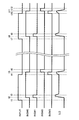
- FIG. 2 is an explanatory diagram illustrating an operation of the laser device 100 according to the first embodiment of the present disclosure.
- FIG. 2 shows a timing chart of the signal INPUT input to the timing generator 120, the signals INSW0 to ISNW3 generated by the timing generator 120 based on the signal INPUT, and the current ILD flowing through the light emitting diode LD1. It is an approximate current waveform.
- the signal INPUT changes from low to high.
- the signals INSW0 and INSW1 generated by the timing generation unit 120 change from low to high.
- the N-type transistors MN3 and MN5 switch from off to on.
- a current flows through the light emitting diode LD1.
- the laser device 100 can speed up the rise of the current ILD flowing through the light emitting diode LD1.
- the signal INSW1 generated by the timing generator 120 changes from high to low.
- the N-type transistor MN5 switches from on to off. The switching of the N-type transistor MN5 from ON to OFF slightly reduces the amount of current ILD flowing through the light emitting diode LD1.
- the signal INPUT changes from high to low. Then, the signal INSW3 generated by the timing generation unit 120 changes from low to high. When the signal INSW3 changes from low to high, the N-type transistor MN7 switches from off to on. When the N-type transistor MN7 switches from off to on, the amount of current ILD flowing through the light emitting diode LD1 increases.
- the signals INSW0 and INSW3 generated by the timing generation unit 120 change from high to low.
- the signal INSW2 generated by the timing generator 120 changes from low to high.
- the N-type transistors MN3 and MN7 switch from on to off.
- the N-type transistors MN3 and MN7 switch from on to off.
- the signal INSW2 switches from low to high at the same timing as the N-type transistors MN3 and MN7 switch from on to off.
- the N-type transistor MN7 switches from off to on, and the amount of current ILD flowing through the light emitting diode LD1 increases. Of the current ILD flowing through the circuit can be accelerated.
- the signal INSW2 generated by the timing generation unit 120 changes from high to low around the point where the current ILD becomes 0.
- the P-type transistor MP0 is turned off.
- the laser device 100 can speed up the rise time and the fall time in the light emitting operation of the light emitting diode LD1 by executing the above-described operation.
- the timing and pulse width of the state transition of each signal shown in FIG. 2 are examples, and are not limited to those shown in FIG.
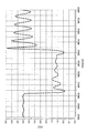
- FIG. 3 is an explanatory diagram illustrating an example of a current waveform of the light emitting diode LD1 in a case where current is drawn from the light emitting diode LD1 only by the driver circuit 150.
- FIG. 4 is a graph showing an example of a current waveform of the light emitting diode LD1 when current is drawn from the light emitting diode LD1 not only from the driver circuit 150 but also from the N-type transistors MN4 and MN5.
- the rise time of the current waveform of the current ILD of the light emitting diode LD1 is faster in FIG. Accordingly, it can be seen that not only the driver circuit 150 but also the N-type transistors MN4 and MN5 draw the current from the light emitting diode LD1, thereby increasing the rise time of the current waveform of the current ILD of the light emitting diode LD1.
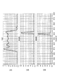
- FIG. 5 is an explanatory diagram showing an example of a change in the potential of the output LDOUT on the cathode side of the light emitting diode LD1.
- FIG. 5 shows an example of a change in the potential of the output LDOUT when the N-type transistors MN6 and MN7 and the P-type transistor MP0 are provided. That is, the current is drawn from the light emitting diode LD1 in the N-type transistors MN6 and MN7 at the timing immediately before the extinction, and the P-type transistor MP0 is turned on at substantially the same timing as the extinction of the light-emitting diode LD1, thereby reducing the cathode potential of the light-emitting diode LD1.
- the power supply is short-circuited, and then the P-type transistor MP0 is turned off.
- the potential of the output LDOUT is temporarily reduced as shown in FIG. Falls, then rises.
- FIG. 6 is an explanatory diagram showing an example of the current waveform of the current ILD of the light emitting diode LD1 and the waveforms of the signals INSW2 and INSW3.
- the current waveform of the current ILD of the light emitting diode LD1 temporarily rises.
- the P-type transistor MP0 is turned on by the signal INSW2, and the cathode potential of the light emitting diode LD1 is short-circuited to the power supply voltage, so that the current ILD sharply decreases to 0 amps.
- the laser device 100 may adjust the rise time and the fall time of the current waveform of the current ILD of the light emitting diode LD1 by adjusting the rise pulses of the signals INSW1, INSW2, and INSW3.
- FIG. 7 is an explanatory diagram showing an example of a change in the potential of the output LDOUT on the cathode side of the light emitting diode LD1.
- FIG. 7 shows an example of a change in the potential of the output LDOUT when the N-type transistors MN6 and MN7 are not provided. As described above, when the N-type transistors MN6 and MN7 are not provided, the potential of the output LDOUT rises to a predetermined potential at the timing of extinction of the light emitting diode LD1 without decreasing the potential of the output LDOUT.
- FIG. 8 is an explanatory diagram showing an example of a current waveform of the current ILD of the light emitting diode LD1.
- FIG. 8 shows an example of the current waveform of the current ILD of the light emitting diode LD1 when the N-type transistors MN6 and MN7 are not provided. As described above, when the N-type transistors MN6 and MN7 are not provided, the current ILD falls to 0 amps at the timing of extinction of the light emitting diode LD1 without a temporary rise in the current waveform.
- N-type transistors MN6 and MN7 are provided, and the amount of current is temporarily increased at the timing of extinction of the light emitting diode LD1.
- the shorter the fall time the better. Therefore, it can be seen that not only the driver circuit 150 but also the N-type transistors MN6 and MN7 draw the current from the light emitting diode LD1 to shorten the fall time of the current waveform of the current ILD of the light emitting diode LD1.
- the laser device 100 can speed up the rise time and the fall time of the current waveform of the current ILD of the light emitting diode LD1.
- the laser device 100 shown in FIG. 1 includes the P-type transistor MP0, and short-circuits the output LDOUT on the cathode side of the light emitting diode LD1 to a predetermined potential at the timing of extinction. It is not limited to.
- FIG. 9 is an explanatory diagram showing a modification of the laser device 100 according to the first embodiment of the present disclosure.
- a level shift circuit including resistors R1 and R2 and N-type transistors MN8 and MN9 are provided to divide the voltage, and the P-type transistor is divided.
- a configuration for reducing the voltage applied to the gate terminal of MP0 may be adopted.
- FIG. 10 is an explanatory diagram showing a modified example of the laser device 100 according to the first embodiment of the present disclosure.
- FIG. 10 shows a configuration in which a capacitive element C1, a resistor R1, and an N-type transistor MN10 are further provided at the gate of the P-type transistor MP0 in the laser device 100 shown in FIG.
- the capacitor C1, the resistor R1, and the N-type transistor MN10 are further provided at the gate of the P-type transistor MP0.
- FIG. 11 is an explanatory diagram illustrating an overall configuration example of the laser device 100 according to the first embodiment of the present disclosure.
- FIG. 11 shows a configuration in which an external controller 160 is added to the laser device 100 shown in FIG.
- FIG. 11 shows a laser device 100 in which four light emitting diodes LD1, LD2, LD3, and LD4 are provided in parallel.
- Light emission of the four light emitting diodes LD1, LD2, LD3, and LD4 is controlled by switch units 110a, 110b, 110c, and 110d, respectively.
- the switches 110a, 110b, 110c, 110d are turned on and off based on a control signal INPUT from the external controller 160.
- the external controller 160 supplies a control signal to the timing generation unit 120.
- the timing generation section 120 generates and outputs signals INSW0 to INSW3 using the control signal INPUT from the external controller 160.
- the laser device 100 has a configuration as illustrated in FIG. 11, so that a light emitting operation and a quenching operation by a plurality of light emitting diodes can be controlled at high speed.
- the laser device 100 capable of further reducing the rise time and the fall time of light emission of the light emitting diode is provided.
- the laser device 100 according to the first embodiment of the present disclosure can shorten the rise time and the fall time of the light emission of the light emitting diode, and can improve the distance measurement accuracy especially when used in a distance measurement sensor.
- the fall time of light emission is shortened by temporarily lowering and then increasing the potential of the cathode side output LDOUT.
- the potential of the cathode-side output LDOUT is once increased and then decreased, so that the rising time of light emission is further reduced. It may have a configuration.
- the current is drawn from the cathode side of the light emitting diode LD1, but the present disclosure is not limited to such an example. Even in the case where a current is input to the anode side of the light emitting diode LD1, it is possible to adopt a structure in which the rising time and the falling time of light emission of the light emitting diode are similarly shortened.
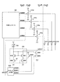
- FIG. 12 is an explanatory diagram illustrating a configuration example of a laser device including a laser drive circuit according to the second embodiment of the present disclosure.
- a configuration example of a laser device including a laser drive circuit according to the second embodiment of the present disclosure will be described with reference to FIG.
- the laser device 200 includes a light emitting diode LD11 and a laser driving circuit for driving the light emitting diode LD11 to emit light.
- the laser drive circuit includes a switch section 210, a timing generation section 220, a current source 230, and a driver circuit 240 including a current mirror including N-type transistors MN0 to MN3 and a switch.
- the laser drive circuit further includes N-type transistors MN4 to MN6.
- the laser device 200 is used, for example, as a ToF distance measuring sensor.
- the ToF distance measuring sensor is a sensor that measures a distance to an object by using a flight time of a laser beam.
- the switch unit 210 has a configuration in which an N-type transistor and a P-type transistor are connected in parallel. When a predetermined signal is applied to the gate of each transistor, ON / OFF of each transistor is switched. The supply of current to the light emitting diode LD11 is controlled by switching on / off of each transistor of the switch unit 210.
- the timing generation unit 220 is a block that generates a signal for controlling on / off switching of the N-type transistors MN0, MN4, and MN5. Each signal is generated from the signal INPUT2 supplied to the timing generation unit 220.
- the signal INSW01 is supplied to the gate of the N-type transistor MN0
- the signal INSW11 is supplied to the gate of the N-type transistor MN4
- the signal INSW2 is supplied to the gate of the N-type transistor MN5.
- the inside of the timing generation unit 220 can be configured by, for example, a delay element or various logic circuits, but is not limited to a specific configuration.
- the current source 230 is a current source for the gates of the N-type transistors MN1 and MN3. The current from the current source 230 turns on the N-type transistors MN1 and MN3.
- the driver circuit 240 is a circuit for driving the light emitting diode LD11 to emit light.
- the light emission of the light emitting diode LD11 is controlled by switching on and off of the N-type transistor MN0 among the transistors shown in the driver circuit 240.
- the switching of the N-type transistor MN0 on and off is controlled by the signal INSW01 from the timing generator 220 as described above.
- the size of the N-type transistor MN0 increases.
- the parasitic capacitance also increases, which affects the rise time and the fall time of the current ILD.
- the laser device 200 has a configuration in which the N-type transistor MN4 is provided in parallel with the N-type transistor MN1.
- the N-type transistor MN4 is provided to make the parasitic capacitance of the N-type transistor MN0 difficult to see.
- a signal that turns on the N-type transistor MN4 is output from the timing generator 220 at the timing of turning off the N-type transistor MN0. Accordingly, the laser device 200 makes it difficult to see the parasitic capacitance of the N-type transistor MN0, and can reduce the fall time of the current ILD of the light emitting diode LD11.
- the driver circuit 240 has a configuration that operates to reduce the gate-source voltage of the N-type transistor MN1 to 0 when the light emitting diode LD11 is extinguished. That is, when the light emitting diode LD11 is extinguished, the driver circuit 240 turns on the N-type transistor MN4, raises the source potential of the N-type transistor MN1, and reduces the gate-source voltage of the N-type transistor MN1 to zero. It is working. Therefore, the N-type transistor MN4 functions as an example of the voltage drop unit of the present disclosure.
- the definitions of the rise time and the fall time in the present embodiment will be described.
- Low @ Level is 0A
- High @ Level is 1A
- the time between 10% and 90% at that level is referred to.
- the laser device 200 shown in FIG. 12 has a configuration in which the light emitting diode LD11 is provided outside the chip, and other circuits are provided inside the chip.
- FIG. 13 is an explanatory diagram illustrating an operation of the laser device 200 according to the second embodiment of the present disclosure.
- FIG. 13 shows a timing chart of the signal INPUT input to the timing generation unit 220, the signals INSW01 to ISNW21 generated by the timing generation unit 220 based on the signal INPUT, and the current ILD flowing through the light emitting diode LD1. It is an approximate current waveform.
- the signal INPUT changes from low to high.
- the signals INSW01 and INSW21 generated by the timing generation unit 220 change from low to high.
- the N-type transistors MN0 and MN5 switch from off to on.
- a current flows through the light emitting diode LD11.
- the laser device 200 can speed up the rise of the current ILD flowing through the light emitting diode LD11.
- the signal INSW21 generated by the timing generation unit 220 changes from high to low.
- the N-type transistor MN5 switches from on to off.
- the amount of the current ILD flowing through the light emitting diode LD11 slightly decreases.
- the signal INPUT changes from high to low.
- the signal INSW01 generated by the timing generation unit 220 changes from high to low.
- the N-type transistor MN0 switches from on to off.
- the amount of the current ILD flowing through the light emitting diode LD11 drops to 0 at a stretch.
- the signal INSW11 generated by the timing generator 220 changes from low to high.
- the N-type transistor MN4 switches from off to on.
- the laser device 200 makes it difficult to see the parasitic capacitance of the N-type transistor MN0 and can reduce the fall time of the current ILD of the light emitting diode LD11.
- the signal INSW11 generated by the timing generation unit 220 changes from high to low.
- the N-type transistor MN4 switches from on to off.
- the laser device 200 can speed up the rise time and the fall time in the light emitting operation of the light emitting diode LD11 by performing the above-described operation.
- the timing and pulse width of the state transition of each signal shown in FIG. 13 are examples, and are not limited to those shown in FIG.
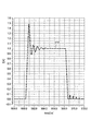
- FIG. 14 is a graph showing an example of the current waveform 271 of the light emitting diode LD1 when the N-type transistor MN4 is provided to cut off the current from the light emitting diode LD1.
- FIG. 15 is a graph showing an example of the current waveform 272 of the light emitting diode LD1 when the current from the light emitting diode LD1 is cut off without providing the N-type transistor MN4.
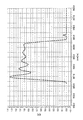
- FIG. 16 is an explanatory diagram showing a graph in which the falling portions of the current waveform 271 shown in FIG. 14 and the current waveform 272 shown in FIG. 15 are overlapped and the horizontal axis is enlarged.
- the laser device 200 can speed up not only the rise time but also the fall time during the light emitting operation of the light emitting diode LD11.
- the fall time of the current ILD of the light emitting diode LD11 is reduced by providing the N-type transistor MN4 and making the parasitic capacitance of the N-type transistor MN0 difficult to see.
- the present disclosure is not limited to such an example.
- FIG. 17 is an explanatory diagram illustrating a modified example of the laser device 200 according to the second embodiment of the present disclosure.
- FIG. 17 shows, as the driver circuit 240 ′, N-type transistors MN0 to MN3 forming a current mirror, an N-type transistor MN7 connected to the gate of the N-type transistor MN1, and a switch SW1. Configuration.
- the signal INSW11 generated by the timing generator 220 is sent to the gate of the N-type transistor MN7 and the switch SW1.
- the signal INSW11 transitions between the high and low states at the same timing as that shown in FIG.
- the driver circuit 240 ′ turns off the N-type transistor MN7 by turning the signal INSW11 from low to high at the timing when the potential of the output LDOUT on the anode side of the light emitting diode LD11 rises when the light emitting diode LD11 is extinguished.
- SW1 is open.
- the driver circuit 240 ' cuts off the connection between the gate of the N-type transistor MN1 and the current source 230 and turns off the N-type transistor MN1.
- the driver circuit 240 ' has a configuration that operates such that the gate-source voltage of the N-type transistor MN1 approaches 0 when the light emitting diode LD11 is extinguished. Therefore, the N-type transistor MN7 and the switch SW1 function as an example of the voltage drop unit of the present disclosure.
- the signal ISNW11 generated by the timing generation unit 220 is input to the N-type transistor MN7 and the switch SW1.
- the laser device 200 shown in FIG. 17 operates as described above, whereby the light emission of the light emitting diode LD11 can be stopped more quickly.
- the laser device 200 according to the second embodiment of the present disclosure may combine the circuit illustrated in FIG. 17 with the N-type transistor MN4 illustrated in FIG.
- FIG. 18 is an explanatory diagram illustrating a modification of the laser device 200 according to the second embodiment of the present disclosure.
- FIG. 18 shows a configuration example of a laser device 200 in which the circuit shown in FIG. 17 is combined with the N-type transistor MN4 shown in FIG.
- the signal ISNW11 generated by the timing generator 220 is input to the N-type transistors MN4 and MN7 and the switch SW1. That is, the N-type transistors MN4 and M7 and the switch SW1 are turned on and off at the same timing.
- the signal ISNW11 generated by the timing generation section 220 is input to the N-type transistors MN4 and MN7 and the switch SW1.
- the laser device 200 shown in FIG. 18 operates as described above, so that the light emission of the light emitting diode LD11 can be stopped more quickly.
- FIG. 19 is an explanatory diagram illustrating an example of the overall configuration of a laser device 200 according to the second embodiment of the present disclosure.
- FIG. 19 shows a configuration in which an external controller 260 is added to the laser device 200 shown in FIG.
- FIG. 19 shows a laser device 100 in which four light emitting diodes LD11, LD12, LD13, and LD14 are provided in parallel.
- the light emission of the four light emitting diodes LD11, LD12, LD13, and LD14 is controlled by the switch units 210a, 210b, 210c, and 210d, respectively.
- the on / off of the switches 210a, 210b, 210c, 210d is performed based on a control signal INPUT2 from the external controller 260. Further, the external controller 260 supplies a control signal INPUT2 to the timing generation unit 220. The timing generation unit 220 generates and outputs signals INSW01 to INSW21 using a control signal from the external controller 260.
- the laser device 200 has a configuration as shown in FIG. 19, so that a light emitting operation and a quenching operation by a plurality of light emitting diodes can be controlled at high speed.
- the laser device 200 capable of further reducing the rise time and the fall time of light emission of the light emitting diode is provided.
- the laser device 200 according to the second embodiment of the present disclosure can shorten the rise time and the fall time of the light emission of the light emitting diode, and can improve the distance measurement accuracy especially when used in a distance measurement sensor.
- the potential of the cathode side output LDOUT is once lowered and then raised to shorten the fall time of light emission.
- the potential of the cathode-side output LDOUT is once increased and then decreased, thereby further shortening the rise time of light emission. It may have a configuration.
- the current is drawn from the cathode side of the light emitting diode LD11.
- the present disclosure is not limited to such an example. Even in the case where a current is input to the anode side of the light emitting diode LD11, a configuration in which the rise time and the fall time of light emission of the light emitting diode can be similarly reduced can be adopted.
- the N-type transistors MN6 and MN7 and the P-type transistor MP0 shown in FIG. 1 may be provided on the cathode side of the light emitting diode LD11. Then, in order to control on / off of the N-type transistor MN7 and the P-type transistor MP0, a configuration in which a signal is supplied from the timing generation unit 220 to the gate of each transistor may be adopted.
- the fall time of the current waveform of the light emitting diode is shortened by temporarily lowering and then increasing the potential of the output on the cathode side when the light emitting diode is quenched.
- a laser device 100 capable of performing the above is provided.
- the fall time of the current waveform of the light emitting diode is reduced by operating to quickly reduce the gate-source voltage of the transistor of the driver circuit to zero.
- a laser device 200 that can be shortened is provided.
- the laser device can improve the ranging accuracy, particularly when used as a ranging sensor, by shortening the fall time of the current waveform of the light emitting diode when the light emitting diode is quenched. It becomes.
- a first drive current unit that adjusts the inflow of current into the light emitting element by a first MOSFET and a second MOSFET connected in series when the light emitting element emits light according to a current amount and when the light emitting element is turned off;
- a voltage drop unit that drops a gate-source voltage of the first MOSFET when the light emitting element is turned off;
- a timing generation unit that generates a signal for controlling driving of the first drive current unit and the voltage drop unit;
- a laser drive circuit comprising: (2)
- the voltage drop unit includes a third MOSFET provided between a source of the first MOSFET and a predetermined potential, The laser drive circuit according to (1), wherein the timing generator outputs a signal for turning on the third MOSFET when the light emitting element is turned off.
- the voltage drop unit includes: A fourth MOSFET provided between a gate of the first MOSFET and a ground potential; A switch provided between a gate of the first MOSFET and a predetermined potential; With The laser drive circuit according to (1) or (2), wherein the timing generation section turns on the fourth MOSFET and outputs a signal to turn off the switch when the light emitting element is turned off. (4) Any of the above (1) to (3), further including a second drive current section provided in parallel with the first drive current section and controlling the flow of current into the light emitting element when the light emitting element emits light. A laser drive circuit according to any one of the above.
- the laser drive circuit according to any one of (1) to (4), wherein the first drive current section and the voltage drop section are provided on a cathode side of the light emitting element.
- a light-emitting element that emits light according to the amount of current;
- a first drive current unit that controls the flow of current into the light emitting element when the light emitting element emits light and when the light is turned off by a first MOSFET;
- a voltage drop unit that drops a gate-source voltage of the first MOSFET when the light emitting element is turned off;
- a timing generation unit that generates a signal for controlling driving of the first drive current unit and the voltage drop unit;
- a sensor device comprising:
Landscapes
- Physics & Mathematics (AREA)
- General Physics & Mathematics (AREA)
- Engineering & Computer Science (AREA)
- Condensed Matter Physics & Semiconductors (AREA)
- Electromagnetism (AREA)
- Optics & Photonics (AREA)
- Computer Networks & Wireless Communication (AREA)
- Radar, Positioning & Navigation (AREA)
- Remote Sensing (AREA)
- Semiconductor Lasers (AREA)
Abstract
電流量に応じて発光する発光素子(LD11)の発光時及び消灯時に前記発光素子への電流の流入を直列に接続された第1MOSFET(MN2)及び第2MOSFET(MN3)により調整する第1の駆動電流部(240)と、前記発光素子の消灯時に前記第1MOSFETのゲートソース間電圧を降下させる電圧降下部(MN4)と、前記第1の駆動電流部及び前記電圧降下部の駆動を制御するための信号を生成するタイミング生成部(220)と、を備える、レーザ駆動回路が提供される。
Description
本開示は、レーザ駆動回路およびセンサ装置に関する。
発光ダイオードの発光駆動を高速化させるためのレーザ駆動回路に関する技術が、例えば特許文献1に記載されている。特許文献1に記載された技術は、発光ダイオードの発光波形の立ち上がり時間及び立ち下がり時間を高速化することで、発光ダイオードの発光駆動を高速化させることを目的としている。
しかし、近年は、レーザ装置のセンシング分野、特に測距センサへの適用が進んでおり、発光ダイオード等の発光素子の発光駆動をより高速化させることが求められている。特にレーザ装置において、発光素子の発光波形の立ち下がり時間については改善の余地が残されている。
そこで、本開示では、特に発光素子の発光波形の立ち下がり時間をより高速化することで、発光素子の発光駆動を高速化させることが可能な、新規かつ改良されたレーザ駆動回路およびセンサ装置を提案する。
本開示によれば、電流量に応じて発光する発光素子の発光時及び消灯時に前記発光素子への電流の流入を直列に接続された第1MOSFET及び第2MOSFETにより調整する第1の駆動電流部と、前記発光素子の消灯時に前記第1MOSFETのゲートソース間電圧を降下させる電圧降下部と、前記第1の駆動電流部及び前記電圧降下部の駆動を制御するための信号を生成するタイミング生成部と、を備える、レーザ駆動回路が提供される。
また本開示によれば、電流量に応じて発光する発光素子と、前記発光素子の発光時及び消灯時に前記発光素子への電流の流入を直列に接続された第1MOSFET及び第2MOSFETにより調整する第1の駆動電流部と、前記発光素子の消灯時に前記第1MOSFETのゲートソース間電圧を降下させる電圧降下部と、前記第1の駆動電流部及び前記電圧降下部の駆動を制御するための信号を生成するタイミング生成部と、を備える、センサ装置が提供される。
以上説明したように本開示によれば、特に発光素子の発光波形の立ち下がり時間をより高速化することで、発光素子の発光駆動を高速化させることが可能な、新規かつ改良されたレーザ駆動回路およびセンサ装置を提供することができる。
なお、上記の効果は必ずしも限定的なものではなく、上記の効果とともに、または上記の効果に代えて、本明細書に示されたいずれかの効果、または本明細書から把握され得る他の効果が奏されてもよい。
以下に添付図面を参照しながら、本開示の好適な実施の形態について詳細に説明する。なお、本明細書及び図面において、実質的に同一の機能構成を有する構成要素については、同一の符号を付することにより重複説明を省略する。
なお、説明は以下の順序で行うものとする。
1.第1の実施の形態
1.1.構成例
1.2.変形例
2.第2の実施の形態
2.1.構成例
2.2.変形例
3.第3の実施の形態
4.まとめ
1.第1の実施の形態
1.1.構成例
1.2.変形例
2.第2の実施の形態
2.1.構成例
2.2.変形例
3.第3の実施の形態
4.まとめ
<1.第1の実施形態>
[1.1.構成例]
まず、本開示の第1の実施の形態に係るレーザ駆動回路及びレーザ駆動回路を備えたレーザ装置について説明する。図1は、本開示の第1の実施形態に係るレーザ駆動回路を備えたレーザ装置の構成例を示す説明図である。以下、図1を用いて本開示の第1の実施形態に係るレーザ駆動回路を備えたレーザ装置の構成例について説明する。
[1.1.構成例]
まず、本開示の第1の実施の形態に係るレーザ駆動回路及びレーザ駆動回路を備えたレーザ装置について説明する。図1は、本開示の第1の実施形態に係るレーザ駆動回路を備えたレーザ装置の構成例を示す説明図である。以下、図1を用いて本開示の第1の実施形態に係るレーザ駆動回路を備えたレーザ装置の構成例について説明する。
図1に示したように、本開示の第1の実施形態に係るレーザ装置100は、発光ダイオードLD1と、発光ダイオードLD1を発光駆動させるためのレーザ駆動回路とを含んで構成される。レーザ駆動回路は、スイッチ部110と、タイミング生成部120と、電流源130と、反転素子140と、N型トランジスタMN0~MN3からなるカレントミラー及びスイッチで構成されるドライバ回路150を、を含んで構成される。レーザ駆動回路は、さらに、P型トランジスタMP0と、N型トランジスタMN4~MN7を含んで構成される。
本開示の第1の実施形態に係るレーザ装置100は、例えばToF(Time of Flight)方式の測距センサとして用いられ得る。ToF方式の測距センサは、レーザ光の飛行時間を用いて対象物との間の距離を測定するセンサである。ToF方式の測距センサには、飛行時間を直接計測することで対象物との間の距離を測定するDirect ToF(D-ToF)方式や、露光量に置き換えて飛行時間を間接的に計測することで対象物との間の距離を測定するInDirect ToF(I-ToF)方式がある。
スイッチ部110は、N型トランジスタとP型トランジスタとが並列に接続された構成を有している。それぞれのトランジスタのゲートに所定の信号が印加されることで、それぞれのトランジスタのオン、オフが切り替わる。スイッチ部110の各トランジスタのオン、オフの切り替わりにより、発光ダイオードLD1への電流の供給が制御される。
タイミング生成部120は、N型トランジスタMN3、MN5、MN7及びP型トランジスタMP0に対するオン、オフの切り替えを制御するための信号を生成するブロックである。それぞれの信号は、タイミング生成部120に供給される信号INPUTから生成される。図1に示した例では、N型トランジスタMN3のゲートには信号INSW0が、N型トランジスタMN5のゲートには信号INSW1が、P型トランジスタMP0のゲートには信号INSW2が、N型トランジスタMN7のゲートには信号INSW3が、それぞれ供給される。タイミング生成部120の内部は、例えば遅延素子や各種論理回路で構成されうるが、後述するようなタイミングで状態が遷移する信号を生成出来るものであれば、特定の構成に限定されるものでは無い。
電流源130は、N型トランジスタMN0、MN2、MN4、MN6のゲートに対する電流源であり、電流源130からの電流により、N型トランジスタMN0、MN2、MN4、MN6をオン状態にしている。反転素子140は、タイミング生成部120からの信号INSW2を反転させて、P型トランジスタMP0のゲートに供給する素子である。なお、N型トランジスタMN4、MN6は、カレントミラー接続でなくても良く、N型トランジスタMN4、MN6のゲートに定電圧が与えられても良い。
ドライバ回路150は、発光ダイオードLD1を発光駆動させるための回路である。ドライバ回路150に示したトランジスタのうち、N型トランジスタMN3のオン、オフが切り替わることにより、発光ダイオードLD1の発光が制御される。N型トランジスタMN3のオン、オフの切り替わりは、上述のようにタイミング生成部120からの信号INSW0によって制御される。
P型トランジスタMP0は、発光ダイオードLD1のカソード側の出力LDOUTを所定の電位に短絡させるために設けられている。具体的には、タイミング生成部120からの信号INSW2が、反転素子140を介してP型トランジスタMP0のゲートに印加されることで、P型トランジスタMP0のオン、オフが切り替わる。P型トランジスタMP0がオンとなることで、発光ダイオードLD1のカソード側の出力LDOUTが所定の電位に短絡される。そしてP型トランジスタMP0がオフとなることで、発光ダイオードLD1のカソード側の出力LDOUTが所定の電位から切り離される。
直列に接続されているN型トランジスタMN4、MN5は、発光ダイオードLD1の発光波形の立ち上がり時間を短縮させるために設けられるトランジスタである。N型トランジスタMN5を、信号INSW1でオンさせることで、ドライバ回路150だけでなく、N型トランジスタMN4、MN5によって発光ダイオードLD1から電流を引き込むことが出来る。ドライバ回路150だけでなく、N型トランジスタMN4、MN5によって発光ダイオードLD1から電流を引き込むことで、発光ダイオードLD1の発光波形の立ち上がり時間を短縮させることが出来る。
一方、直列に接続されているN型トランジスタMN6、MN7は、発光ダイオードLD1の発光波形の立ち下がり時間を短縮させるために設けられるトランジスタである。本実施形態では、発光ダイオードLD1を消灯させる際に、N型トランジスタMN6、MN7によって発光ダイオードLD1に流す電流を一旦増加させている。すなわち、N型トランジスタMN7を、信号INSW3でオンさせることで、ドライバ回路150だけでなく、N型トランジスタMN6、MN7によって発光ダイオードLD1から電流を引き込む。これにより、発光ダイオードLD1に流す電流が一時的に増加する。発光ダイオードLD1を消灯させる際に、発光ダイオードLD1に流す電流を一旦増加させ、その後、P型トランジスタMP0がオンすることにより、発光ダイオードLD1のカソード側の出力LDOUTが所定の電位に短絡されることで、発光ダイオードLD1の発光波形の立ち下がり時間を短縮させることが可能となる。
ここで、本実施形態における立ち上がり時間と立ち下がり時間の定義を示す。本実施形態では、Low Levelを0A、High Levelを1Aとして、そのレベルでの10%~90%の間の時間をいう。レーザが発光および消光するには電流閾値が存在する。特にレーサ装置を測距センサとして用いた場合には、その電流閾値を高速に通過させることが測距精度に繋がる。よって、立ち上がり時間と立ち下がり時間をできる限り短くする事が重要となる。
図1に示したレーザ装置100は、発光ダイオードLD1がチップの外に設けられ、その他の回路がチップ内に設けられる構成を有する。
以上、図1を用いて本開示の第1の実施形態に係るレーザ装置100の構成例を説明した。続いて、本開示の第1の実施形態に係るレーザ装置100の動作を説明する。
図2は、本開示の第1の実施形態に係るレーザ装置100の動作を示す説明図である。図2に示したのは、タイミング生成部120に入力される信号INPUTと、タイミング生成部120が信号INPUTに基づき生成する信号INSW0~ISNW3とのタイミングチャート、および、発光ダイオードLD1が流す電流ILDのおおよその電流波形である。
まず時刻t1で、信号INPUTがローからハイとなる。すると、続く時刻t2の時点で、タイミング生成部120が生成する信号INSW0、INSW1がローからハイとなる。信号INSW0、INSW1がローからハイとなることで、N型トランジスタMN3、MN5がオフからオンに切り替わる。N型トランジスタMN3、MN5がオフからオンに切り替わることで発光ダイオードLD1に電流が流れる。ここで、N型トランジスタMN3だけでなく、N型トランジスタMN5も同時にオンにすることで、レーザ装置100は発光ダイオードLD1に流れる電流ILDの立ち上がりを高速化することができる。
続く時刻t3の時点で、タイミング生成部120が生成する信号INSW1がハイからローとなる。信号INSW1がハイからローとなることで、N型トランジスタMN5がオンからオフに切り替わる。N型トランジスタMN5がオンからオフに切り替わることで、発光ダイオードLD1に流れる電流ILDの量はやや低下する。
続く時刻t4の時点で、信号INPUTがハイからローとなる。すると、タイミング生成部120が生成する信号INSW3がローからハイとなる。信号INSW3がローからハイとなることで、N型トランジスタMN7がオフからオンに切り替わる。N型トランジスタMN7がオフからオンに切り替わることで発光ダイオードLD1に流れる電流ILDの量が増加する。
続く時刻t5の時点で、タイミング生成部120が生成する信号INSW0、INSW3がハイからローとなる。また時刻t5の時点で、タイミング生成部120が生成する信号INSW2がローからハイとなる。信号INSW0、INSW3がハイからローとなることで、N型トランジスタMN3、MN7がオンからオフに切り替わる。N型トランジスタMN3、MN7がオンからオフに切り替わる。N型トランジスタMN3、MN7がオンからオフに切り替わるのと同じタイミングで、信号INSW2がローからハイに切り替わる。この2つの動作により、発光ダイオードLD1に流れる電流ILDの量が0まで一気に低下する。すなわち、消光の直前のタイミングで(上述の時刻t4の時点で)N型トランジスタMN7がオフからオンに切り替わり、発光ダイオードLD1に流れる電流ILDの量が増加することで、レーザ装置100は発光ダイオードLD1に流れる電流ILDの立ち下がりを高速化することができる。
また信号INSW2がローからハイに切り替わることで、P型トランジスタMP0がオンとなり、発光ダイオードLD1のカソード側の出力LDOUTが所定の電位に短絡される。
続く時刻t6の時点の、電流ILDが0になる辺りでタイミング生成部120が生成する信号INSW2がハイからローとなる。信号INSW2がハイからローに切り替わることで、P型トランジスタMP0がオフとなる。
その後、時刻t7~t12において、同様の動作が繰り返される。
本開示の第1の実施形態に係るレーザ装置100は、上述の動作を実行することで、発光ダイオードLD1の発光動作時の立ち上がり時間及び立ち下がり時間を高速化させることができる。なお、図2に示した各信号の状態遷移のタイミングおよびパルス幅は一例であり、図2に示したものに限定されるものではない。
本開示の第1の実施形態に係るレーザ装置100の効果について説明する。図3は、ドライバ回路150だけで発光ダイオードLD1から電流を引き込む場合の、発光ダイオードLD1の電流波形の例をグラフで示す説明図である。また図4は、ドライバ回路150だけでなく、N型トランジスタMN4、MN5からも発光ダイオードLD1から電流を引き込む場合の、発光ダイオードLD1の電流波形の例をグラフで示す説明図である。
図3と図4とを比較すると、発光ダイオードLD1の電流ILDの電流波形の立ち上がり時間が、図4の方が速くなっている。従って、ドライバ回路150だけでなく、N型トランジスタMN4、MN5においても発光ダイオードLD1から電流を引き込むことで、発光ダイオードLD1の電流ILDの電流波形の立ち上がり時間が早くなっていることがわかる。
図5は、発光ダイオードLD1のカソード側の出力LDOUTの電位の変化例を示す説明図である。図5に示したのは、N型トランジスタMN6、MN7及びP型トランジスタMP0を設けた場合の出力LDOUTの電位の変化例である。すなわち、消光の直前のタイミングでN型トランジスタMN6、MN7において発光ダイオードLD1から電流を引き込み、発光ダイオードLD1の消光とほぼ同じタイミングで、P型トランジスタMP0をオンさせることで発光ダイオードLD1のカソード電位を電源に短絡し、その後P型トランジスタMP0をオフしている。このように、消光の直前のタイミングでN型トランジスタMN6、MN7において発光ダイオードLD1から電流を引き込み、P型トランジスタMP0をオンさせると、図5に示したように、出力LDOUTの電位が一時的に低下し、その後上昇する。
図6は、発光ダイオードLD1の電流ILDの電流波形と、信号INSW2、INSW3の波形との例を示す説明図である。図6に示したように、信号INSW3をN型トランジスタMN7のゲートに出力することで、発光ダイオードLD1の電流ILDの電流波形が一時的に持ち上がる。その後、P型トランジスタMP0を信号INSW2でオンさせて、発光ダイオードLD1のカソード電位が電源電圧に短絡されることで、電流ILDは急激に0アンペアまで低下する。
レーザ装置100は、信号INSW1、INSW2、INSW3の立ち上がりパルスの調整により、発光ダイオードLD1の電流ILDの電流波形の立ち上がり時間と立ち下がり時間を調整しても良い。
比較のために、N型トランジスタMN6、MN7を設けない場合の出力LDOUTの電位の変化例、および、発光ダイオードLD1の電流ILDの電流波形の例を説明する。
図7は、発光ダイオードLD1のカソード側の出力LDOUTの電位の変化例を示す説明図である。図7に示したのは、N型トランジスタMN6、MN7を設けない場合の出力LDOUTの電位の変化例である。このように、N型トランジスタMN6、MN7を設けない場合では、発光ダイオードLD1の消光のタイミングで、出力LDOUTの電位が低下しないまま、所定の電位へ上昇する。
図8は、発光ダイオードLD1の電流ILDの電流波形の例を示す説明図である。図8に示したのは、N型トランジスタMN6、MN7を設けない場合の発光ダイオードLD1の電流ILDの電流波形の例である。このように、N型トランジスタMN6、MN7を設けない場合では、電流ILDは、発光ダイオードLD1の消光のタイミングで、電流波形が一時的に持ち上がることなく、0アンペアまで低下する。
図6に示した波形と図8に示した波形とを比較すると、図6に示したように、N型トランジスタMN6、MN7を設け、発光ダイオードLD1の消光のタイミングで電流量を一時的に増加させた方が、立ち下がり時間が短くなる。従って、ドライバ回路150だけでなく、N型トランジスタMN6、MN7においても発光ダイオードLD1から電流を引き込むことで、発光ダイオードLD1の電流ILDの電流波形の立ち下がり時間が早くなっていることがわかる。
以上説明したように、本開示の第1の実施形態に係るレーザ装置100は、発光ダイオードLD1の電流ILDの電流波形の立ち上がり時間及び立ち下がり時間を高速化させることができる。
[1.2.変形例] 図1に示したレーザ装置100は、P型トランジスタMP0を設けて、消光のタイミングで発光ダイオードLD1のカソード側の出力LDOUTを所定の電位に短絡させていたが、本開示は係る例に限定されるものでは無い。
図9は、本開示の第1の実施形態に係るレーザ装置100の変形例を示す説明図である。P型トランジスタMP0のゲート端子の耐圧では信号INSW2を受けられない場合には、例えば抵抗R1、R2からなるレベルシフト回路と、N型トランジスタMN8、MN9と、を設けて分圧して、P型トランジスタMP0のゲート端子に印加する電圧を低下させる構成を採用しても良い。
図10は、本開示の第1の実施形態に係るレーザ装置100の変形例を示す説明図である。図10に示したのは、図1に示したレーザ装置100におけるP型トランジスタMP0のゲートに、容量素子C1と、抵抗R1と、N型トランジスタMN10と、をさらに設けた構成である。P型トランジスタMP0のゲート端子の耐圧では信号INSW2を受けられない場合には、このように、P型トランジスタMP0のゲートに、容量素子C1と、抵抗R1と、N型トランジスタMN10と、をさらに設けた構成であっても、電流ILDの電流波形の立ち下がり時間を高速化させることができる。
図11は、本開示の第1の実施形態に係るレーザ装置100の全体構成例を示す説明図である。図11には、図1に示したレーザ装置100において外部コントローラ160が追加された構成が示されている。また図11には、4つの発光ダイオードLD1、LD2、LD3、LD4が並列に設けられたレーザ装置100が示されている。4つの発光ダイオードLD1、LD2、LD3、LD4は、それぞれスイッチ部110a、110b、110c、110dによって発光が制御される。スイッチ部110a、110b、110c、110dのオン、オフは、外部コントローラ160からの制御信号INPUTに基づいて行われる。また外部コントローラ160は、タイミング生成部120に対して制御信号を供給する。タイミング生成部120は、外部コントローラ160からの制御信号INPUTを用いて信号INSW0~INSW3を生成し、出力する。
本開示の第1の実施形態に係るレーザ装置100は、図11に示したような構成を有することで、複数の発光ダイオードによる発光動作および消光動作を高速に制御することが可能となる。
以上説明したように本開示の第1の実施形態によれば、発光ダイオードの発光の立ち上がり時間及び立ち下がり時間をより短縮させることが可能なレーザ装置100が提供される。本開示の第1の実施形態に係るレーザ装置100は、発光ダイオードの発光の立ち上がり時間及び立ち下がり時間を短縮できることで、特に測距センサに用いた場合に測距制度を向上させることができる。
上述した実施例では、発光ダイオードLD1の消光時に、カソード側の出力LDOUTの電位を一旦下げてから上昇させることで、発光の立ち下がり時間の短縮を図っていた。本開示の第1の実施形態に係るレーザ装置100は、発光ダイオードLD1の発光時に、カソード側の出力LDOUTの電位を一旦上げてから下降させることで、発光の立ち上がり時間のさらなる短縮を図るような構成を有していても良い。
上述した実施例では、発光ダイオードLD1のカソード側から電流を引き込む構成としていたが、本開示は係る例に限定されるものでは無い。発光ダイオードLD1のアノード側に電流を入力する構成とした場合であっても、同様に発光ダイオードの発光の立ち上がり時間及び立ち下がり時間をより短縮させる構成を採ることが可能である。
<2.第2の実施形態>
[2.1.構成例] 続いて、本開示の第2の実施の形態に係るレーザ駆動回路及びレーザ駆動回路を備えたレーザ装置について説明する。図12は、本開示の第2の実施形態に係るレーザ駆動回路を備えたレーザ装置の構成例を示す説明図である。以下、図12を用いて本開示の第2の実施形態に係るレーザ駆動回路を備えたレーザ装置の構成例について説明する。
[2.1.構成例] 続いて、本開示の第2の実施の形態に係るレーザ駆動回路及びレーザ駆動回路を備えたレーザ装置について説明する。図12は、本開示の第2の実施形態に係るレーザ駆動回路を備えたレーザ装置の構成例を示す説明図である。以下、図12を用いて本開示の第2の実施形態に係るレーザ駆動回路を備えたレーザ装置の構成例について説明する。
図12に示したように、本開示の第2の実施形態に係るレーザ装置200は、発光ダイオードLD11と、発光ダイオードLD11を発光駆動させるためのレーザ駆動回路とを含んで構成される。レーザ駆動回路は、スイッチ部210と、タイミング生成部220と、電流源230と、N型トランジスタMN0~MN3からなるカレントミラー及びスイッチで構成されるドライバ回路240と、を含んで構成される。レーザ駆動回路は、さらに、N型トランジスタMN4~MN6を含んで構成される。
本開示の第2の実施形態に係るレーザ装置200は、例えばToF方式の測距センサとして用いられる。ToF方式の測距センサは、レーザ光の飛行時間を用いて対象物との間の距離を測定するセンサである。
スイッチ部210は、N型トランジスタとP型トランジスタとが並列に接続された構成を有している。それぞれのトランジスタのゲートに所定の信号が印加されることで、それぞれのトランジスタのオン、オフが切り替わる。スイッチ部210の各トランジスタのオン、オフの切り替わりにより、発光ダイオードLD11への電流の供給が制御される。
タイミング生成部220は、N型トランジスタMN0、MN4、MN5に対するオン、オフの切り替えを制御するための信号を生成するブロックである。それぞれの信号は、タイミング生成部220に供給される信号INPUT2から生成される。図12に示した例では、N型トランジスタMN0のゲートには信号INSW01が、N型トランジスタMN4のゲートには信号INSW11が、N型トランジスタMN5のゲートには信号INSW2が、それぞれ供給される。タイミング生成部220の内部は、例えば遅延素子や各種論理回路で構成されうるが、特定の構成に限定されるものでは無い。
電流源230は、N型トランジスタMN1、MN3のゲートに対する電流源であり、電流源230からの電流により、N型トランジスタMN1、MN3をオン状態にしている。
ドライバ回路240は、発光ダイオードLD11を発光駆動させるための回路である。ドライバ回路240に示したトランジスタのうち、N型トランジスタMN0のオン、オフが切り替わることにより、発光ダイオードLD11の発光が制御される。N型トランジスタMN0のオン、オフの切り替わりは、上述のようにタイミング生成部220からの信号INSW01によって制御される。
ここで、発光ダイオードLD11の電流ILDの立ち下がり時間を短縮させるためには、電流ILDを素早く止めることが求められる。また発光ダイオードLD11の発光のために電流ILDが大きくなるため、N型トランジスタMN0のサイズは大きくなる。しかし、N型トランジスタMN0のサイズを大きくすると、寄生容量も増加してしまい、電流ILDの立ち上がり時間及び立ち下がり時間に影響を与えてしまう。
そこで本開示の第2の実施形態に係るレーザ装置200は、N型トランジスタMN1と並列にN型トランジスタMN4を設けた構成を有する。N型トランジスタMN4は、N型トランジスタMN0の寄生容量を見えにくくするために設けられる。具体的には後述するが、N型トランジスタMN0をオフするタイミングで、N型トランジスタMN4をオンするような信号をタイミング生成部220から出力する。これによりレーザ装置200は、N型トランジスタMN0の寄生容量を見えにくくして、発光ダイオードLD11の電流ILDの立ち下がり時間を短縮させることができる。
言い換えれば、ドライバ回路240は、発光ダイオードLD11を消光させる際に、N型トランジスタMN1のゲート-ソース間電圧を0に低下させるよう動作する構成を有する。すなわちドライバ回路240は、発光ダイオードLD11を消光させる際にN型トランジスタMN4をオンさせて、N型トランジスタMN1のソース電位を持ち上げて、N型トランジスタMN1のゲート-ソース間電圧を0に低下させるよう動作している。従って、N型トランジスタMN4は、本開示の電圧降下部の一例として機能する。
ここで、本実施形態における立ち上がり時間と立ち下がり時間の定義を示す。本実施形態では、Low Levelを0A、High Levelを1Aとして、そのレベルでの10%~90%の間の時間をいう。レーザが発光および消光するには電流閾値が存在する。その電流閾値を高速に通過させることが、特にレーサ装置を測距センサとして用いた場合には測距精度に繋がる。よって、立ち上がり時間と立ち下がり時間を早くする事が重要となる。
図12に示したレーザ装置200は、発光ダイオードLD11がチップの外に設けられ、その他の回路がチップ内に設けられる構成を有する。
以上、図12を用いて本開示の第2の実施形態に係るレーザ装置200の構成例を説明した。続いて、本開示の第2の実施形態に係るレーザ装置200の動作を説明する。
図13は、本開示の第2の実施形態に係るレーザ装置200の動作を示す説明図である。図13に示したのは、タイミング生成部220に入力される信号INPUTと、タイミング生成部220が信号INPUTに基づき生成する信号INSW01~ISNW21とのタイミングチャート、および、発光ダイオードLD1が流す電流ILDのおおよその電流波形である。
まず時刻t1で、信号INPUTがローからハイとなる。すると、続く時刻t2の時点で、タイミング生成部220が生成する信号INSW01、INSW21がローからハイとなる。信号INSW01、INSW21がローからハイとなることで、N型トランジスタMN0、MN5がオフからオンに切り替わる。N型トランジスタMN0、MN5がオフからオンに切り替わることで発光ダイオードLD11に電流が流れる。ここで、N型トランジスタMN0だけでなく、N型トランジスタMN5も同時にオンにすることで、レーザ装置200は発光ダイオードLD11に流れる電流ILDの立ち上がりを高速化することができる。
続く時刻t3の時点で、タイミング生成部220が生成する信号INSW21がハイからローとなる。信号INSW21がハイからローとなることで、N型トランジスタMN5がオンからオフに切り替わる。N型トランジスタMN5がオンからオフに切り替わることで、発光ダイオードLD11に流れる電流ILDの量はやや低下する。
続く時刻t4の時点で、信号INPUTがハイからローとなる。すると、続く時刻t5の時点で、タイミング生成部220が生成する信号INSW01がハイからローとなる。信号INSW01がハイからローとなることで、N型トランジスタMN0がオンからオフに切り替わる。N型トランジスタMN0がオンからオフに切り替わることで、発光ダイオードLD11に流れる電流ILDの量が0まで一気に低下する。
また時刻t5の時点で、タイミング生成部220が生成する信号INSW11がローからハイとなる。信号INSW11がローからハイとなることで、N型トランジスタMN4がオフからオンに切り替わる。N型トランジスタMN4をオンすることで、レーザ装置200は、N型トランジスタMN0の寄生容量を見えにくくして、発光ダイオードLD11の電流ILDの立ち下がり時間を短縮させることができる。
その後、時刻t6の時点でタイミング生成部220が生成する信号INSW11がハイからローとなる。信号INSW11がハイからローとなることで、N型トランジスタMN4がオンからオフに切り替わる。
その後、時刻t7~t12において、同様の動作が繰り返される。
本開示の第2の実施形態に係るレーザ装置200は、上述の動作を実行することで、発光ダイオードLD11の発光動作時の立ち上がり時間及び立ち下がり時間を高速化させることができる。なお、図13に示した各信号の状態遷移のタイミングおよびパルス幅は一例であり、図13に示したものに限定されるものではない。
本開示の第2の実施形態に係るレーザ装置200の効果について説明する。図14は、N型トランジスタMN4を設けて発光ダイオードLD1からの電流を遮断する場合の、発光ダイオードLD1の電流波形271の例をグラフで示す説明図である。また図15は、N型トランジスタMN4を設けずに発光ダイオードLD1からの電流を遮断する場合の、発光ダイオードLD1の電流波形272の例をグラフで示す説明図である。そして図16は、図14に示した電流波形271と図15に示した電流波形272との立ち下がり部分を重ね合わせ、横軸を拡大したグラフを示す説明図である。
図16に示したように、N型トランジスタMN4を設けて発光ダイオードLD1からの電流を遮断した電流波形271の方が、電流波形272よりも立ち下がりが早くなっていることが分かる。従って、本開示の第2の実施形態に係るレーザ装置200は、発光ダイオードLD11の発光動作時の立ち上がり時間だけでなく、立ち下がり時間をも高速化させることができる。
[2.2.変形例]
本開示の第2の実施形態に係るレーザ装置200は、N型トランジスタMN4を設けて、N型トランジスタMN0の寄生容量を見えにくくすることで、発光ダイオードLD11の電流ILDの立ち下がり時間を短縮させていたが、本開示は係る例に限定されるものではない。
本開示の第2の実施形態に係るレーザ装置200は、N型トランジスタMN4を設けて、N型トランジスタMN0の寄生容量を見えにくくすることで、発光ダイオードLD11の電流ILDの立ち下がり時間を短縮させていたが、本開示は係る例に限定されるものではない。
図17は、本開示の第2の実施形態に係るレーザ装置200の変形例を示す説明図である。図17に示したのは、ドライバ回路240’として、カレントミラーを構成するN型トランジスタMN0~MN3と、N型トランジスタMN1のゲートに接続されているN型トランジスタMN7と、スイッチSW1と、が備えられている構成である。N型トランジスタMN7のゲートおよびスイッチSW1には、タイミング生成部220が生成する信号INSW11が送られる。信号INSW11は、図13に示したものと同じタイミングでハイおよびローの状態が遷移する。
ドライバ回路240’は、発光ダイオードLD11を消光させる際に、発光ダイオードLD11のアノード側の出力LDOUTの電位が立ち上がるタイミングで信号INSW11がローからハイとなることで、N型トランジスタMN7がオンとなり、スイッチSW1をオープンにしている。そしてドライバ回路240’は、スイッチSW1をオープンにすることで、N型トランジスタMN1のゲートと電流源230との接続を遮断し、N型トランジスタMN1をオフさせるよう動作する。言い換えれば、ドライバ回路240’は、発光ダイオードLD11を消光させる際に、N型トランジスタMN1のゲート-ソース間電圧を0に近付けるよう動作する構成を有する。従って、N型トランジスタMN7及びスイッチSW1は、本開示の電圧降下部の一例として機能する。
具体的には、図13に示したタイミングチャートと同様に、タイミング生成部220で生成される信号ISNW11が、N型トランジスタMN7、及びスイッチSW1に入力される。図17に示したレーザ装置200は、このように動作することで、発光ダイオードLD11の発光の停止を速めることが出来る。
本開示の第2の実施形態に係るレーザ装置200は、図17に示した回路と、図12で示したN型トランジスタMN4とを組み合わせてもよい。図18は、本開示の第2の実施形態に係るレーザ装置200の変形例を示す説明図である。図18に示したのは、図17に示した回路と、図12で示したN型トランジスタMN4とを組み合わせた、レーザ装置200の構成例である。
図18に示したレーザ装置200は、タイミング生成部220で生成される信号ISNW11が、N型トランジスタMN4、MN7、及びスイッチSW1に入力される。すなわち、N型トランジスタMN4、M7、及びスイッチSW1は、同一のタイミングでオン、オフが切り替わる。具体的には、図13に示したタイミングチャートと同様に、タイミング生成部220で生成される信号ISNW11が、N型トランジスタMN4、MN7、及びスイッチSW1に入力される。図18に示したレーザ装置200は、このように動作することで、発光ダイオードLD11の発光の停止を速めることが出来る。
図19は、本開示の第2の実施形態に係るレーザ装置200の全体構成例を示す説明図である。図19には、図12に示したレーザ装置200において外部コントローラ260が追加された構成が示されている。また図19には、4つの発光ダイオードLD11、LD12、LD13、LD14が並列に設けられたレーザ装置100が示されている。4つの発光ダイオードLD11、LD12、LD13、LD14は、それぞれスイッチ部210a、210b、210c、210dによって発光が制御される。スイッチ部210a、210b、210c、210dのオン、オフは、外部コントローラ260からの制御信号INPUT2に基づいて行われる。また外部コントローラ260は、タイミング生成部220に対して制御信号INPUT2を供給する。タイミング生成部220は、外部コントローラ260からの制御信号を用いて信号INSW01~INSW21を生成し、出力する。
本開示の第2の実施形態に係るレーザ装置200は、図19に示したような構成を有することで、複数の発光ダイオードによる発光動作および消光動作を高速に制御することが可能となる。
以上説明したように本開示の第2の実施形態によれば、発光ダイオードの発光の立ち上がり時間及び立ち下がり時間をより短縮させることが可能なレーザ装置200が提供される。本開示の第2の実施形態に係るレーザ装置200は、発光ダイオードの発光の立ち上がり時間及び立ち下がり時間を短縮できることで、特に測距センサに用いた場合に測距制度を向上させることができる。
上述した実施例では、発光ダイオードLD11の消光時に、カソード側の出力LDOUTの電位を一旦下げてから上昇させることで、発光の立ち下がり時間の短縮を図っていた。本開示の第2の実施形態に係るレーザ装置200は、発光ダイオードLD11の発光時に、カソード側の出力LDOUTの電位を一旦上げてから下降させることで、発光の立ち上がり時間のさらなる短縮を図るような構成を有していても良い。
上述した実施例では、発光ダイオードLD11のカソード側から電流を引き込む構成としていたが、本開示は係る例に限定されるものでは無い。発光ダイオードLD11のアノード側に電流を入力する構成とした場合であっても、同様に発光ダイオードの発光の立ち上がり時間及び立ち下がり時間をより短縮させる構成を採ることが可能である。
<3.第3の実施形態>
上述した本開示の第1の実施形態では、発光ダイオードの消光時に、カソード側の出力の電位を一旦下げてから上昇させることで、発光ダイオードの電流波形の立ち下がり時間の短縮を図っていた。そして本開示の第2の実施形態では、発光ダイオードの消光時に、ドライバ回路のトランジスタのゲート-ソース間電圧を素早く0に近付けるよう動作することで、発光ダイオードの電流波形の立ち下がり時間の短縮を図っていた。従って、上述した第1の実施形態の構成と、第2の実施形態の構成の両方を有するレーザ装置が提供されても良い。
上述した本開示の第1の実施形態では、発光ダイオードの消光時に、カソード側の出力の電位を一旦下げてから上昇させることで、発光ダイオードの電流波形の立ち下がり時間の短縮を図っていた。そして本開示の第2の実施形態では、発光ダイオードの消光時に、ドライバ回路のトランジスタのゲート-ソース間電圧を素早く0に近付けるよう動作することで、発光ダイオードの電流波形の立ち下がり時間の短縮を図っていた。従って、上述した第1の実施形態の構成と、第2の実施形態の構成の両方を有するレーザ装置が提供されても良い。
すなわち、図12に示したレーザ装置200において、発光ダイオードLD11のカソード側に、図1に示したN型トランジスタMN6、7と、P型トランジスタMP0とを設けても良い。そして、N型トランジスタMN7及びP型トランジスタMP0のオン、オフを制御するために、タイミング生成部220から信号をそれぞれのトランジスタのゲートに信号を供給する構成が採用されても良い。
<4.まとめ>
以上説明したように、本開示の第1の実施形態では、発光ダイオードの消光時に、カソード側の出力の電位を一旦下げてから上昇させることで、発光ダイオードの電流波形の立ち下がり時間を短縮させることが可能なレーザ装置100が提供される。また、本開示の第2の実施形態では、発光ダイオードの消光時に、ドライバ回路のトランジスタのゲート-ソース間電圧を素早く0に低下させるよう動作することで、発光ダイオードの電流波形の立ち下がり時間を短縮させることが可能なレーザ装置200が提供される。
以上説明したように、本開示の第1の実施形態では、発光ダイオードの消光時に、カソード側の出力の電位を一旦下げてから上昇させることで、発光ダイオードの電流波形の立ち下がり時間を短縮させることが可能なレーザ装置100が提供される。また、本開示の第2の実施形態では、発光ダイオードの消光時に、ドライバ回路のトランジスタのゲート-ソース間電圧を素早く0に低下させるよう動作することで、発光ダイオードの電流波形の立ち下がり時間を短縮させることが可能なレーザ装置200が提供される。
上述した各実施形態に係るレーザ装置は、発光ダイオードの消光時に、発光ダイオードの電流波形の立ち下がり時間を短縮させることで、特に測距センサとして用いた場合に測距精度を向上させることが可能となる。
以上、添付図面を参照しながら本開示の好適な実施形態について詳細に説明したが、本開示の技術的範囲はかかる例に限定されない。本開示の技術分野における通常の知識を有する者であれば、請求の範囲に記載された技術的思想の範疇内において、各種の変更例または修正例に想到し得ることは明らかであり、これらについても、当然に本開示の技術的範囲に属するものと了解される。
また、本明細書に記載された効果は、あくまで説明的または例示的なものであって限定的ではない。つまり、本開示に係る技術は、上記の効果とともに、または上記の効果に代えて、本明細書の記載から当業者には明らかな他の効果を奏しうる。
なお、以下のような構成も本開示の技術的範囲に属する。
(1)
電流量に応じて発光する発光素子の発光時及び消灯時に前記発光素子への電流の流入を直列に接続された第1MOSFET及び第2MOSFETにより調整する第1の駆動電流部と、
前記発光素子の消灯時に前記第1MOSFETのゲートソース間電圧を降下させる電圧降下部と、
前記第1の駆動電流部及び前記電圧降下部の駆動を制御するための信号を生成するタイミング生成部と、
を備える、レーザ駆動回路。
(2)
前記電圧降下部は、前記第1MOSFETのソースと所定の電位との間に設けられる第3MOSFETを備え、
前記タイミング生成部は、前記発光素子の消灯時に前記第3MOSFETをオンさせる信号を出力する、前記(1)に記載のレーザ駆動回路。
(3)
前記電圧降下部は、
前記第1MOSFETのゲートとグランド電位との間に設けられる第4MOSFETと、
前記第1MOSFETのゲートと所定の電位との間に設けられるスイッチと、
を備え、
前記タイミング生成部は、前記発光素子の消灯時に前記第4MOSFETをオンさせ、前記スイッチをオフさせる信号を出力する、前記(1)または(2)に記載のレーザ駆動回路。
(4)
前記第1の駆動電流部と並列に設けられ、前記発光素子の発光時に前記発光素子への電流の流入を制御する第2の駆動電流部をさらに備える、前記(1)~(3)のいずれかに記載のレーザ駆動回路。
(5)
前記第1の駆動電流部及び前記電圧降下部は、前記発光素子のカソード側に設けられる、前記(1)~(4)のいずれかに記載のレーザ駆動回路。
(6)
電流量に応じて発光する発光素子と、
前記発光素子の発光時及び消灯時に前記発光素子への電流の流入を第1MOSFETにより制御する第1の駆動電流部と、
前記発光素子の消灯時に前記第1MOSFETのゲートソース間電圧を降下させる電圧降下部と、
前記第1の駆動電流部及び前記電圧降下部の駆動を制御するための信号を生成するタイミング生成部と、
を備える、センサ装置。
(1)
電流量に応じて発光する発光素子の発光時及び消灯時に前記発光素子への電流の流入を直列に接続された第1MOSFET及び第2MOSFETにより調整する第1の駆動電流部と、
前記発光素子の消灯時に前記第1MOSFETのゲートソース間電圧を降下させる電圧降下部と、
前記第1の駆動電流部及び前記電圧降下部の駆動を制御するための信号を生成するタイミング生成部と、
を備える、レーザ駆動回路。
(2)
前記電圧降下部は、前記第1MOSFETのソースと所定の電位との間に設けられる第3MOSFETを備え、
前記タイミング生成部は、前記発光素子の消灯時に前記第3MOSFETをオンさせる信号を出力する、前記(1)に記載のレーザ駆動回路。
(3)
前記電圧降下部は、
前記第1MOSFETのゲートとグランド電位との間に設けられる第4MOSFETと、
前記第1MOSFETのゲートと所定の電位との間に設けられるスイッチと、
を備え、
前記タイミング生成部は、前記発光素子の消灯時に前記第4MOSFETをオンさせ、前記スイッチをオフさせる信号を出力する、前記(1)または(2)に記載のレーザ駆動回路。
(4)
前記第1の駆動電流部と並列に設けられ、前記発光素子の発光時に前記発光素子への電流の流入を制御する第2の駆動電流部をさらに備える、前記(1)~(3)のいずれかに記載のレーザ駆動回路。
(5)
前記第1の駆動電流部及び前記電圧降下部は、前記発光素子のカソード側に設けられる、前記(1)~(4)のいずれかに記載のレーザ駆動回路。
(6)
電流量に応じて発光する発光素子と、
前記発光素子の発光時及び消灯時に前記発光素子への電流の流入を第1MOSFETにより制御する第1の駆動電流部と、
前記発光素子の消灯時に前記第1MOSFETのゲートソース間電圧を降下させる電圧降下部と、
前記第1の駆動電流部及び前記電圧降下部の駆動を制御するための信号を生成するタイミング生成部と、
を備える、センサ装置。
100、200 レーザ装置
110、210 スイッチ部
130、230 電流源
140 反転素子
150、240 ドライバ回路
LD1、LD11 発光ダイオード
110、210 スイッチ部
130、230 電流源
140 反転素子
150、240 ドライバ回路
LD1、LD11 発光ダイオード
Claims (6)
- 電流量に応じて発光する発光素子の発光時及び消灯時に前記発光素子への電流の流入を直列に接続された第1MOSFET及び第2MOSFETにより調整する第1の駆動電流部と、
前記発光素子の消灯時に前記第1MOSFETのゲートソース間電圧を降下させる電圧降下部と、
前記第1の駆動電流部及び前記電圧降下部の駆動を制御するための信号を生成するタイミング生成部と、
を備える、レーザ駆動回路。 - 前記電圧降下部は、前記第1MOSFETのソースと所定の電位との間に設けられる第3MOSFETを備え、
前記タイミング生成部は、前記発光素子の消灯時に前記第3MOSFETをオンさせる信号を出力する、請求項1に記載のレーザ駆動回路。 - 前記電圧降下部は、
前記第1MOSFETのゲートとグランド電位との間に設けられる第4MOSFETと、
前記第1MOSFETのゲートと所定の電位との間に設けられるスイッチと、
を備え、
前記タイミング生成部は、前記発光素子の消灯時に前記第4MOSFETをオンさせ、前記スイッチをオフさせる信号を出力する、請求項1に記載のレーザ駆動回路。 - 前記第1の駆動電流部と並列に設けられ、前記発光素子の発光時に前記発光素子への電流の流入を制御する第2の駆動電流部をさらに備える、請求項1に記載のレーザ駆動回路。
- 前記第1の駆動電流部及び前記電圧降下部は、前記発光素子のカソード側に設けられる、請求項1に記載のレーザ駆動回路。
- 電流量に応じて発光する発光素子と、
前記発光素子の発光時及び消灯時に前記発光素子への電流の流入を直列に接続された第1MOSFET及び第2MOSFETにより調整する第1の駆動電流部と、
前記発光素子の消灯時に前記第1MOSFETのゲートソース間電圧を降下させる電圧降下部と、
前記第1の駆動電流部及び前記電圧降下部の駆動を制御するための信号を生成するタイミング生成部と、
を備える、センサ装置。
Priority Applications (1)
| Application Number | Priority Date | Filing Date | Title |
|---|---|---|---|
| US17/250,309 US11996675B2 (en) | 2018-07-10 | 2019-06-17 | Laser drive circuit and sensor apparatus |
Applications Claiming Priority (4)
| Application Number | Priority Date | Filing Date | Title |
|---|---|---|---|
| JP2018-130714 | 2018-07-10 | ||
| JP2018-130713 | 2018-07-10 | ||
| JP2018130713A JP2021168314A (ja) | 2018-07-10 | 2018-07-10 | レーザ駆動回路およびセンサ装置 |
| JP2018130714A JP2021168315A (ja) | 2018-07-10 | 2018-07-10 | レーザ駆動回路およびセンサ装置 |
Publications (1)
| Publication Number | Publication Date |
|---|---|
| WO2020012880A1 true WO2020012880A1 (ja) | 2020-01-16 |
Family
ID=69142688
Family Applications (1)
| Application Number | Title | Priority Date | Filing Date |
|---|---|---|---|
| PCT/JP2019/023980 Ceased WO2020012880A1 (ja) | 2018-07-10 | 2019-06-17 | レーザ駆動回路およびセンサ装置 |
Country Status (2)
| Country | Link |
|---|---|
| US (1) | US11996675B2 (ja) |
| WO (1) | WO2020012880A1 (ja) |
Cited By (4)
| Publication number | Priority date | Publication date | Assignee | Title |
|---|---|---|---|---|
| FR3119250A1 (fr) * | 2021-01-22 | 2022-07-29 | Stmicroelectronics (Grenoble 2) Sas | Pilote côté bas pour diode laser |
| WO2024184951A1 (ja) * | 2023-03-03 | 2024-09-12 | 日清紡マイクロデバイス株式会社 | 半導体レーザ駆動装置 |
| WO2025164386A1 (ja) * | 2024-01-30 | 2025-08-07 | ソニーセミコンダクタソリューションズ株式会社 | 光源駆動装置、発光装置及び測距システム |
| WO2025164349A1 (ja) * | 2024-01-30 | 2025-08-07 | ソニーセミコンダクタソリューションズ株式会社 | 光源駆動装置、発光装置及び測距システム |
Families Citing this family (1)
| Publication number | Priority date | Publication date | Assignee | Title |
|---|---|---|---|---|
| US20230411927A1 (en) * | 2022-06-15 | 2023-12-21 | Ii-Vi Delaware, Inc. | Edge rate (rise and fall time) controlled segmented laser driver |
Citations (5)
| Publication number | Priority date | Publication date | Assignee | Title |
|---|---|---|---|---|
| JP2004039748A (ja) * | 2002-07-01 | 2004-02-05 | Sumitomo Electric Ind Ltd | 半導体レーザ駆動回路 |
| JP2006339507A (ja) * | 2005-06-03 | 2006-12-14 | Rohm Co Ltd | 駆動回路およびそれを備えた携帯情報端末 |
| JP2010141138A (ja) * | 2008-12-11 | 2010-06-24 | Kagoshima Univ | レーザーダイオード駆動装置 |
| JP2014232746A (ja) * | 2013-05-28 | 2014-12-11 | 株式会社リコー | 光源駆動回路、光走査装置及び画像形成装置 |
| US20180083419A1 (en) * | 2016-09-16 | 2018-03-22 | Stmicroelectronics (Research & Development) Limited | Apparatus |
Family Cites Families (4)
| Publication number | Priority date | Publication date | Assignee | Title |
|---|---|---|---|---|
| JP3668612B2 (ja) * | 1998-06-29 | 2005-07-06 | 株式会社東芝 | 光半導体素子駆動回路及び光送受信モジュール |
| JP3769180B2 (ja) * | 2000-09-26 | 2006-04-19 | 株式会社東芝 | 発光ダイオード駆動回路およびそれを用いた光送信モジュール |
| US9183873B2 (en) * | 2011-09-26 | 2015-11-10 | Texas Instruments Incorporated | Laser diode driver damping circuit |
| US9472921B2 (en) * | 2015-01-16 | 2016-10-18 | Macom Technology Solutions Holdings, Inc. | Split voltage supply configuration with matched input load for single ended drivers |
-
2019
- 2019-06-17 US US17/250,309 patent/US11996675B2/en active Active
- 2019-06-17 WO PCT/JP2019/023980 patent/WO2020012880A1/ja not_active Ceased
Patent Citations (5)
| Publication number | Priority date | Publication date | Assignee | Title |
|---|---|---|---|---|
| JP2004039748A (ja) * | 2002-07-01 | 2004-02-05 | Sumitomo Electric Ind Ltd | 半導体レーザ駆動回路 |
| JP2006339507A (ja) * | 2005-06-03 | 2006-12-14 | Rohm Co Ltd | 駆動回路およびそれを備えた携帯情報端末 |
| JP2010141138A (ja) * | 2008-12-11 | 2010-06-24 | Kagoshima Univ | レーザーダイオード駆動装置 |
| JP2014232746A (ja) * | 2013-05-28 | 2014-12-11 | 株式会社リコー | 光源駆動回路、光走査装置及び画像形成装置 |
| US20180083419A1 (en) * | 2016-09-16 | 2018-03-22 | Stmicroelectronics (Research & Development) Limited | Apparatus |
Cited By (5)
| Publication number | Priority date | Publication date | Assignee | Title |
|---|---|---|---|---|
| FR3119250A1 (fr) * | 2021-01-22 | 2022-07-29 | Stmicroelectronics (Grenoble 2) Sas | Pilote côté bas pour diode laser |
| US12374862B2 (en) | 2021-01-22 | 2025-07-29 | Stmicroelectronics (Grenoble 2) Sas | Low side driver for laser diode |
| WO2024184951A1 (ja) * | 2023-03-03 | 2024-09-12 | 日清紡マイクロデバイス株式会社 | 半導体レーザ駆動装置 |
| WO2025164386A1 (ja) * | 2024-01-30 | 2025-08-07 | ソニーセミコンダクタソリューションズ株式会社 | 光源駆動装置、発光装置及び測距システム |
| WO2025164349A1 (ja) * | 2024-01-30 | 2025-08-07 | ソニーセミコンダクタソリューションズ株式会社 | 光源駆動装置、発光装置及び測距システム |
Also Published As
| Publication number | Publication date |
|---|---|
| US11996675B2 (en) | 2024-05-28 |
| US20210273404A1 (en) | 2021-09-02 |
Similar Documents
| Publication | Publication Date | Title |
|---|---|---|
| WO2020012880A1 (ja) | レーザ駆動回路およびセンサ装置 | |
| US7724072B2 (en) | Voltage generator of semiconductor integrated circuit | |
| TWI743555B (zh) | 基於GaN之可調電流驅動器電路 | |
| CN114089313B (zh) | 用于激光雷达的发光装置的驱动装置和激光雷达 | |
| JP2003202830A (ja) | 駆動回路 | |
| US10311784B2 (en) | Pixel driver circuit, display device and pixel driving method | |
| EP2201820B1 (en) | Driver for light emitting semiconductor device | |
| US9813051B2 (en) | Driving circuit for power switch | |
| JP2014067240A (ja) | 半導体装置 | |
| CN114185052B (zh) | 激光发射驱动电路及激光雷达 | |
| CN109417273B (zh) | 生成信号脉冲以用于操作发光二极管的驱动电路 | |
| US8305122B2 (en) | Laser diode driver | |
| JP2013187528A (ja) | 発光素子駆動装置 | |
| JP2021168314A (ja) | レーザ駆動回路およびセンサ装置 | |
| JP5791355B2 (ja) | 発光素子の駆動回路 | |
| JP2021168315A (ja) | レーザ駆動回路およびセンサ装置 | |
| KR102320544B1 (ko) | 레벨 쉬프터 | |
| WO2021031808A1 (zh) | 驱动电路、驱动方法、瞬态增强型ldo电路、cmos驱动器电源电路和激光器系统 | |
| JP2006157400A (ja) | ドライバ回路 | |
| CN118642070A (zh) | 激光雷达及其光发射装置的驱动电路、控制方法、存储介质 | |
| KR101306865B1 (ko) | 고전압 집적회로 | |
| KR20140002915A (ko) | 전원 회로 | |
| CN114554650B (zh) | Led驱动电路及其偏置电压生成器、led照明装置 | |
| CN112271917A (zh) | 一种可用于低边驱动的限流电路 | |
| US12470121B2 (en) | Fail-safe input/output device and voltage switching method |
Legal Events
| Date | Code | Title | Description |
|---|---|---|---|
| 121 | Ep: the epo has been informed by wipo that ep was designated in this application |
Ref document number: 19833937 Country of ref document: EP Kind code of ref document: A1 |
|
| NENP | Non-entry into the national phase |
Ref country code: DE |
|
| 122 | Ep: pct application non-entry in european phase |
Ref document number: 19833937 Country of ref document: EP Kind code of ref document: A1 |
|
| NENP | Non-entry into the national phase |
Ref country code: JP |