WO2020008802A1 - 固体撮像装置 - Google Patents
固体撮像装置 Download PDFInfo
- Publication number
- WO2020008802A1 WO2020008802A1 PCT/JP2019/022709 JP2019022709W WO2020008802A1 WO 2020008802 A1 WO2020008802 A1 WO 2020008802A1 JP 2019022709 W JP2019022709 W JP 2019022709W WO 2020008802 A1 WO2020008802 A1 WO 2020008802A1
- Authority
- WO
- WIPO (PCT)
- Prior art keywords
- electrode
- imaging device
- photoelectric conversion
- charge transfer
- transfer control
- Prior art date
- Legal status (The legal status is an assumption and is not a legal conclusion. Google has not performed a legal analysis and makes no representation as to the accuracy of the status listed.)
- Ceased
Links
Images




















Classifications
-
- H—ELECTRICITY
- H10—SEMICONDUCTOR DEVICES; ELECTRIC SOLID-STATE DEVICES NOT OTHERWISE PROVIDED FOR
- H10F—INORGANIC SEMICONDUCTOR DEVICES SENSITIVE TO INFRARED RADIATION, LIGHT, ELECTROMAGNETIC RADIATION OF SHORTER WAVELENGTH OR CORPUSCULAR RADIATION
- H10F39/00—Integrated devices, or assemblies of multiple devices, comprising at least one element covered by group H10F30/00, e.g. radiation detectors comprising photodiode arrays
- H10F39/80—Constructional details of image sensors
- H10F39/803—Pixels having integrated switching, control, storage or amplification elements
-
- H—ELECTRICITY
- H04—ELECTRIC COMMUNICATION TECHNIQUE
- H04N—PICTORIAL COMMUNICATION, e.g. TELEVISION
- H04N25/00—Circuitry of solid-state image sensors [SSIS]; Control thereof
- H04N25/40—Extracting pixel data from image sensors by controlling scanning circuits, e.g. by modifying the number of pixels sampled or to be sampled
- H04N25/46—Extracting pixel data from image sensors by controlling scanning circuits, e.g. by modifying the number of pixels sampled or to be sampled by combining or binning pixels
-
- H—ELECTRICITY
- H10—SEMICONDUCTOR DEVICES; ELECTRIC SOLID-STATE DEVICES NOT OTHERWISE PROVIDED FOR
- H10F—INORGANIC SEMICONDUCTOR DEVICES SENSITIVE TO INFRARED RADIATION, LIGHT, ELECTROMAGNETIC RADIATION OF SHORTER WAVELENGTH OR CORPUSCULAR RADIATION
- H10F39/00—Integrated devices, or assemblies of multiple devices, comprising at least one element covered by group H10F30/00, e.g. radiation detectors comprising photodiode arrays
- H10F39/10—Integrated devices
- H10F39/12—Image sensors
-
- H—ELECTRICITY
- H04—ELECTRIC COMMUNICATION TECHNIQUE
- H04N—PICTORIAL COMMUNICATION, e.g. TELEVISION
- H04N25/00—Circuitry of solid-state image sensors [SSIS]; Control thereof
- H04N25/70—SSIS architectures; Circuits associated therewith
- H04N25/76—Addressed sensors, e.g. MOS or CMOS sensors
-
- H—ELECTRICITY
- H04—ELECTRIC COMMUNICATION TECHNIQUE
- H04N—PICTORIAL COMMUNICATION, e.g. TELEVISION
- H04N25/00—Circuitry of solid-state image sensors [SSIS]; Control thereof
- H04N25/70—SSIS architectures; Circuits associated therewith
- H04N25/76—Addressed sensors, e.g. MOS or CMOS sensors
- H04N25/77—Pixel circuitry, e.g. memories, A/D converters, pixel amplifiers, shared circuits or shared components
- H04N25/778—Pixel circuitry, e.g. memories, A/D converters, pixel amplifiers, shared circuits or shared components comprising amplifiers shared between a plurality of pixels, i.e. at least one part of the amplifier must be on the sensor array itself
-
- H—ELECTRICITY
- H04—ELECTRIC COMMUNICATION TECHNIQUE
- H04N—PICTORIAL COMMUNICATION, e.g. TELEVISION
- H04N25/00—Circuitry of solid-state image sensors [SSIS]; Control thereof
- H04N25/70—SSIS architectures; Circuits associated therewith
- H04N25/79—Arrangements of circuitry being divided between different or multiple substrates, chips or circuit boards, e.g. stacked image sensors
-
- H—ELECTRICITY
- H10—SEMICONDUCTOR DEVICES; ELECTRIC SOLID-STATE DEVICES NOT OTHERWISE PROVIDED FOR
- H10F—INORGANIC SEMICONDUCTOR DEVICES SENSITIVE TO INFRARED RADIATION, LIGHT, ELECTROMAGNETIC RADIATION OF SHORTER WAVELENGTH OR CORPUSCULAR RADIATION
- H10F39/00—Integrated devices, or assemblies of multiple devices, comprising at least one element covered by group H10F30/00, e.g. radiation detectors comprising photodiode arrays
- H10F39/10—Integrated devices
- H10F39/12—Image sensors
- H10F39/18—Complementary metal-oxide-semiconductor [CMOS] image sensors; Photodiode array image sensors
- H10F39/182—Colour image sensors
-
- H—ELECTRICITY
- H10—SEMICONDUCTOR DEVICES; ELECTRIC SOLID-STATE DEVICES NOT OTHERWISE PROVIDED FOR
- H10F—INORGANIC SEMICONDUCTOR DEVICES SENSITIVE TO INFRARED RADIATION, LIGHT, ELECTROMAGNETIC RADIATION OF SHORTER WAVELENGTH OR CORPUSCULAR RADIATION
- H10F39/00—Integrated devices, or assemblies of multiple devices, comprising at least one element covered by group H10F30/00, e.g. radiation detectors comprising photodiode arrays
- H10F39/80—Constructional details of image sensors
- H10F39/802—Geometry or disposition of elements in pixels, e.g. address-lines or gate electrodes
- H10F39/8023—Disposition of the elements in pixels, e.g. smaller elements in the centre of the imager compared to larger elements at the periphery
-
- H—ELECTRICITY
- H10—SEMICONDUCTOR DEVICES; ELECTRIC SOLID-STATE DEVICES NOT OTHERWISE PROVIDED FOR
- H10F—INORGANIC SEMICONDUCTOR DEVICES SENSITIVE TO INFRARED RADIATION, LIGHT, ELECTROMAGNETIC RADIATION OF SHORTER WAVELENGTH OR CORPUSCULAR RADIATION
- H10F39/00—Integrated devices, or assemblies of multiple devices, comprising at least one element covered by group H10F30/00, e.g. radiation detectors comprising photodiode arrays
- H10F39/80—Constructional details of image sensors
- H10F39/812—Arrangements for transferring the charges in the image sensor perpendicular to the imaging plane, e.g. buried regions used to transfer generated charges to circuitry under the photosensitive region
-
- H—ELECTRICITY
- H10—SEMICONDUCTOR DEVICES; ELECTRIC SOLID-STATE DEVICES NOT OTHERWISE PROVIDED FOR
- H10F—INORGANIC SEMICONDUCTOR DEVICES SENSITIVE TO INFRARED RADIATION, LIGHT, ELECTROMAGNETIC RADIATION OF SHORTER WAVELENGTH OR CORPUSCULAR RADIATION
- H10F39/00—Integrated devices, or assemblies of multiple devices, comprising at least one element covered by group H10F30/00, e.g. radiation detectors comprising photodiode arrays
- H10F39/80—Constructional details of image sensors
- H10F39/813—Electronic components shared by multiple pixels, e.g. one amplifier shared by two pixels
-
- H—ELECTRICITY
- H10—SEMICONDUCTOR DEVICES; ELECTRIC SOLID-STATE DEVICES NOT OTHERWISE PROVIDED FOR
- H10F—INORGANIC SEMICONDUCTOR DEVICES SENSITIVE TO INFRARED RADIATION, LIGHT, ELECTROMAGNETIC RADIATION OF SHORTER WAVELENGTH OR CORPUSCULAR RADIATION
- H10F39/00—Integrated devices, or assemblies of multiple devices, comprising at least one element covered by group H10F30/00, e.g. radiation detectors comprising photodiode arrays
- H10F39/10—Integrated devices
- H10F39/12—Image sensors
- H10F39/18—Complementary metal-oxide-semiconductor [CMOS] image sensors; Photodiode array image sensors
- H10F39/182—Colour image sensors
- H10F39/1825—Multicolour image sensors having stacked structure, e.g. NPN, NPNPN or multiple quantum well [MQW] structures
-
- H—ELECTRICITY
- H10—SEMICONDUCTOR DEVICES; ELECTRIC SOLID-STATE DEVICES NOT OTHERWISE PROVIDED FOR
- H10F—INORGANIC SEMICONDUCTOR DEVICES SENSITIVE TO INFRARED RADIATION, LIGHT, ELECTROMAGNETIC RADIATION OF SHORTER WAVELENGTH OR CORPUSCULAR RADIATION
- H10F39/00—Integrated devices, or assemblies of multiple devices, comprising at least one element covered by group H10F30/00, e.g. radiation detectors comprising photodiode arrays
- H10F39/10—Integrated devices
- H10F39/12—Image sensors
- H10F39/191—Photoconductor image sensors
-
- H—ELECTRICITY
- H10—SEMICONDUCTOR DEVICES; ELECTRIC SOLID-STATE DEVICES NOT OTHERWISE PROVIDED FOR
- H10F—INORGANIC SEMICONDUCTOR DEVICES SENSITIVE TO INFRARED RADIATION, LIGHT, ELECTROMAGNETIC RADIATION OF SHORTER WAVELENGTH OR CORPUSCULAR RADIATION
- H10F39/00—Integrated devices, or assemblies of multiple devices, comprising at least one element covered by group H10F30/00, e.g. radiation detectors comprising photodiode arrays
- H10F39/80—Constructional details of image sensors
- H10F39/803—Pixels having integrated switching, control, storage or amplification elements
- H10F39/8037—Pixels having integrated switching, control, storage or amplification elements the integrated elements comprising a transistor
-
- H—ELECTRICITY
- H10—SEMICONDUCTOR DEVICES; ELECTRIC SOLID-STATE DEVICES NOT OTHERWISE PROVIDED FOR
- H10F—INORGANIC SEMICONDUCTOR DEVICES SENSITIVE TO INFRARED RADIATION, LIGHT, ELECTROMAGNETIC RADIATION OF SHORTER WAVELENGTH OR CORPUSCULAR RADIATION
- H10F39/00—Integrated devices, or assemblies of multiple devices, comprising at least one element covered by group H10F30/00, e.g. radiation detectors comprising photodiode arrays
- H10F39/80—Constructional details of image sensors
- H10F39/811—Interconnections
-
- H—ELECTRICITY
- H10—SEMICONDUCTOR DEVICES; ELECTRIC SOLID-STATE DEVICES NOT OTHERWISE PROVIDED FOR
- H10K—ORGANIC ELECTRIC SOLID-STATE DEVICES
- H10K39/00—Integrated devices, or assemblies of multiple devices, comprising at least one organic radiation-sensitive element covered by group H10K30/00
- H10K39/30—Devices controlled by radiation
- H10K39/32—Organic image sensors
Definitions
- the present disclosure relates to a solid-state imaging device.
- An image sensor using an organic semiconductor material for the photoelectric conversion layer can photoelectrically convert a specific color (wavelength band). Because of these features, when used as an imaging device in a solid-state imaging device, subpixels are formed from a combination of an on-chip color filter (OCCF) and an imaging device, and the subpixels are two-dimensionally arranged. It is possible to obtain a structure in which sub-pixels are stacked (stacked image sensor), which is impossible with a conventional solid-state imaging device (see, for example, JP-A-2017-157816). Further, since demosaic processing is not required, there is an advantage that a false color does not occur.
- OCCF on-chip color filter
- an imaging device provided with a photoelectric conversion unit provided on or above a semiconductor substrate is referred to as a “first type imaging device” for convenience, and a photoelectric device constituting the first type imaging device is referred to as a “first type imaging device”.
- the conversion unit is referred to as a “first type photoelectric conversion unit” for convenience, and the imaging device provided in the semiconductor substrate is referred to as a “second type imaging device” for convenience, forming a second type imaging device.
- Such a photoelectric conversion unit may be referred to as a “second type photoelectric conversion unit” for convenience.
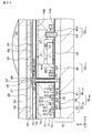
- FIG. 51 shows an example of the structure of a stacked image sensor (stacked solid-state imaging device) disclosed in JP-A-2017-157816.
- a third photoelectric conversion unit 43 that is a second type photoelectric conversion unit that constitutes the third imaging device 15 and the second imaging device 13 that are the second imaging device is provided in the semiconductor substrate 70.
- the second photoelectric conversion unit 41 are stacked and formed.
- a first photoelectric conversion unit 11 ' which is a first type of photoelectric conversion unit, is disposed above the semiconductor substrate 70 (specifically, above the second imaging element 13).
- the first photoelectric conversion unit 11 ′ includes a first electrode 21, a photoelectric conversion layer 23 made of an organic material, and a second electrode 22, and constitutes the first imaging element 11 which is a first type imaging element. I do. Further, a charge storage electrode 24 is provided separately from the first electrode 21, and the photoelectric conversion layer 23 is located above the charge storage electrode 24 via an insulating layer 82.
- the second photoelectric conversion unit 41 and the third photoelectric conversion unit 43 for example, blue light and red light are photoelectrically converted, respectively, due to a difference in absorption coefficient.
- green light is photoelectrically converted.
- the charges generated by the photoelectric conversion in the second photoelectric conversion unit 41 and the third photoelectric conversion unit 43 are temporarily stored in the second photoelectric conversion unit 41 and the third photoelectric conversion unit 43, respectively, and then each of the vertical transistors ( transferred by illustrating the gate portion 45) and the transfer transistor (illustrating the gate portion 46) to the second floating diffusion region (floating diffusion) FD 2 and the third floating diffusion layer FD 3, further external readout circuit (FIG. (Not shown).
- These transistors and the floating diffusion layers FD 2 and FD 3 are also formed on the semiconductor substrate 70.
- the charge generated by the photoelectric conversion in the first photoelectric conversion unit 11 ′ is attracted to the charge storage electrode 24 and stored in the photoelectric conversion layer 23 during charge storage.
- charge accumulated in the photoelectric conversion layer 23 is stored first electrode 21, the contact hole 61, via the wiring layer 62, the first floating diffusion layer FD 1 formed on the semiconductor substrate 70 .
- the first photoelectric conversion unit 11 ′ is also connected to a gate unit 52 of an amplification transistor that converts a charge amount into a voltage via a contact hole 61 and a wiring layer 62.
- the first floating diffusion layer FD 1 constitutes a part of the reset transistor (illustrating the gate portion 51).
- the reference numerals 63, 64, 65, 66, 71, 72, 76, 81, 83, 90 and the like will be described in a fourth embodiment.
- FIG. 51 shows a simplified configuration and structure of the first imaging device 11, the second imaging device 13, and the third imaging device 15.
- four image pickup devices 11, 13, and 15 are 1
- One first electrode and one floating diffusion layer FD 1 , FD 2 , FD 3 are shared.
- 52A and 52B two of the four first image sensors are illustrated. Two image sensors not shown are provided behind the two image sensors shown in the drawing.
- the image pickup element block 10 1 by the first image sensor 11 11, 11 12 and a total of four first image sensor of the two first image sensor (not shown) is configured
- the first image sensor 11 13, 11 14 and not shown imaging device block 10 2 is constituted by two total of four first image sensor of the first image sensor.
- the imaging element blocks 12 1 by the second image pickup element 13 11, 13 12 and a total of four second imaging element two second image sensor (not shown) is configured
- the second imaging element 13 13, 13 14 and not shown image sensor block 12 2 is constituted by two total of four second imaging element of the second image sensor.
- the imaging element blocks 14 1 by a total of four third imaging device of the third image pickup element 15 11, 15 12 and not shown two third imaging device is configured, the third image sensor 15 13, 15 14 and not shown image sensor block 14 2 is constituted by two total of four third imaging device of the third image pickup device.
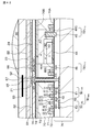
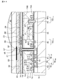
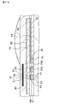
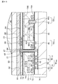
- this arrangement in the imaging device structure, may be subject on the relationship between the layout constraints on the arrangement of the first floating diffusion layer FD 1 and the contact hole 61. Therefore, as shown in a schematic partial cross-sectional view in FIG. 52B, for example, the first image sensor 11 is shifted by one image sensor with respect to the second image sensor 13 and the third image sensor 15. Form.
- the barycentric coordinates of the addition signal obtained from the second image sensor block 12 1, 3 are aligned to the center of gravity coordinates of the addition signal obtained from the image pickup element block 14 1, but taken from the first image sensor block 10 1
- the coordinates of the center of gravity of the added signal deviate, which hinders the subsequent image processing.
- the signals obtained by the second image sensor block 12 1 and the third image sensor block 14 1 can be added, but the signals obtained by the first image sensor block 10 1 cannot be added thereto. .
- an object of the present disclosure is to provide a solid-state imaging device having a configuration and structure that can add signals obtained by a plurality of photoelectric conversion elements in order to increase sensitivity and that are not easily restricted by layout. To provide.
- a solid-state imaging device for achieving the above object, It has a plurality of image sensor blocks each including P ⁇ Q (where P ⁇ 2, Q ⁇ 1) image sensors, Each image sensor has a photoelectric conversion layer, an insulating layer, and a photoelectric conversion unit including a charge storage electrode disposed to face the photoelectric conversion layer with the insulating layer interposed therebetween.
- a first charge transfer control electrode is provided between the imaging device and the imaging device
- a second charge transfer control electrode is provided between the imaging device block and the imaging device block
- P imaging devices are arranged along a first direction
- Q imaging devices are arranged along a second direction
- the charge accumulated in the photoelectric conversion layer of the (P-1) -th imaging device from the first imaging device along the first direction is the P-th imaging device. It is transferred to the photoelectric conversion layer of the element and is read out together with the charges accumulated in the photoelectric conversion layers of the Q Pth imaging elements.
- a solid-state imaging device for achieving the above object includes a stacked-type imaging device having at least one imaging device included in the solid-state imaging device according to the first embodiment of the present disclosure. ing.
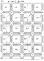
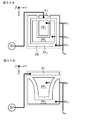
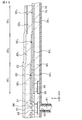
- FIG. 1 is a diagram schematically illustrating an arrangement state of an imaging element block, a charge storage electrode, a first charge transfer control electrode, a second charge transfer control electrode, and a first electrode in the solid-state imaging device according to the first embodiment.
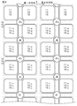
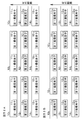
- FIG. 2 is a diagram schematically illustrating an arrangement state of an imaging element block and a two-layer lower imaging element block in the solid-state imaging device according to the first embodiment.
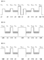
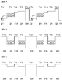
- FIGS. 3A, 3B, and 3C are diagrams schematically showing a potential applied to each electrode and a charge (electron) accumulation state during the charge accumulation period in the solid-state imaging device according to the first embodiment.
- FIGS. 1 is a diagram schematically illustrating an arrangement state of an imaging element block, a charge storage electrode, a first charge transfer control electrode, a second charge transfer control electrode, and a first electrode in the solid-state imaging device according to the first embodiment.
- FIG. 2 is a diagram schematically illustrating an arrangement state of an imaging element block and a two-layer lower imaging element block
- FIGS. 5A, 5B, and 5C are diagrams schematically showing a potential applied to each electrode and an accumulation state of charges (electrons) immediately after the start of the first charge transfer period in the solid-state imaging device according to the first embodiment. is there.
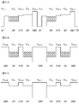
- FIGS. 5A, 5B, and 5C are diagrams schematically showing a potential applied to each electrode and an accumulation state of charges (electrons) immediately before the end of the first charge transfer period in the solid-state imaging device according to the first embodiment.
- 6A, 6B, and 6C are diagrams schematically illustrating the potential applied to each electrode and the accumulation state of charges (electrons) during the second charge transfer period in the solid-state imaging device according to the first embodiment.
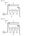
- FIG. 7 is a diagram schematically illustrating an arrangement state of an imaging element block, a charge storage electrode, a first charge transfer control electrode, a second charge transfer control electrode, and a first electrode in the solid-state imaging device according to the second embodiment.
- FIG. 8 is a diagram schematically illustrating an arrangement state of an imaging element block, a charge storage electrode, a first charge transfer control electrode, a second charge transfer control electrode, and a first electrode in the solid-state imaging device according to the third embodiment.
- FIG. 9 is a diagram schematically illustrating an arrangement state of an imaging element block, a charge storage electrode, a first charge transfer control electrode, a second charge transfer control electrode, and a first electrode in a modification of the solid-state imaging device according to the third embodiment. It is.
- FIG. 8 is a diagram schematically illustrating an arrangement state of an imaging element block, a charge storage electrode, a first charge transfer control electrode, a second charge transfer control electrode, and a first electrode in a modification of the solid-state imaging device according to the
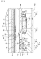
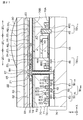
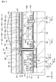
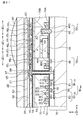
- FIG. 10 is a schematic cross-sectional view of a part of the image sensor (two image sensors arranged side by side) of the fourth embodiment.
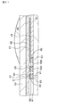
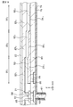
- FIG. 11 is a schematic partial cross-sectional view of one of the imaging device and the stacked imaging device of the fourth embodiment.
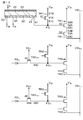
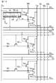
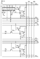
- FIG. 12 is an equivalent circuit diagram of the imaging device and the stacked imaging device of the fourth embodiment.
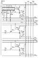
- FIG. 13 is an equivalent circuit diagram of the imaging device and the stacked imaging device of the fourth embodiment.
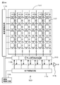
- FIG. 14 is a conceptual diagram of the solid-state imaging device according to the fourth embodiment.
- FIG. 15 is an equivalent circuit diagram of a modified example (modified example 1 of the fourth embodiment) of the imaging device and the stacked-type imaging device of the fourth embodiment.
- FIG. 16 is a schematic cross-sectional view of a modification (modification 2 of Example 4) of the image sensor of Example 4 (two image sensors arranged side by side).
- 17A and 17B are schematic cross-sectional views of an image sensor (two image sensors arranged side by side) of Example 5 and a part of a modified example thereof.
- FIG. 18 is a schematic partial cross-sectional view of the imaging device and the stacked imaging device of the sixth embodiment.
- FIG. 19 is a schematic partial cross-sectional view of the imaging device and the stacked imaging device of the seventh embodiment.
- FIG. 20 is a schematic partial cross-sectional view of a modified example of the imaging device and the stacked imaging device of the seventh embodiment.
- FIG. 21 is a schematic partial cross-sectional view of a part of the imaging device and the stacked imaging device according to the eighth embodiment.
- FIG. 22 is an equivalent circuit diagram of the imaging device and the stacked imaging device of the eighth embodiment.
- FIG. 23 is an equivalent circuit diagram of the imaging device and the stacked imaging device of the eighth embodiment.
- FIG. 24 is a schematic partial cross-sectional view of a part of the imaging device and the stacked imaging device of the ninth embodiment.
- FIG. 25 is an equivalent circuit diagram of the imaging device and the stacked imaging device of the ninth embodiment.
- FIG. 26 is an equivalent circuit diagram of the imaging device and the stacked imaging device of the ninth embodiment.
- FIG. 27 is a schematic partial cross-sectional view of the imaging device and the stacked imaging device of Example 10.
- FIG. 28 is a schematic partial cross-sectional view in which the portion where the charge storage electrode, the photoelectric conversion layer, and the second electrode are stacked in the imaging element of Example 10 is enlarged.
- FIG. 29 is a schematic partial cross-sectional view in which the portion where the charge storage electrode, the photoelectric conversion layer, and the second electrode are stacked in the imaging element of Example 11 is enlarged.
- FIG. 30 is a schematic partial cross-sectional view of the imaging device and the stacked imaging device of Example 12.
- FIG. 31 is a schematic partial cross-sectional view of the imaging devices of Example 13 and Example 14, and the stacked imaging device.
- 32A and 32B are schematic plan views of a charge storage electrode segment according to the fourteenth embodiment.
- FIG. 33A and 33B are schematic plan views of a charge storage electrode segment according to the fourteenth embodiment.
- FIG. 34 is a schematic partial cross-sectional view of the imaging devices of Examples 15 and 14 and the stacked imaging device.
- 35A and 35B are schematic plan views of a charge storage electrode segment according to the fifteenth embodiment.
- FIG. 36 is a diagram schematically illustrating an arrangement state of charge storage electrodes and the like in the solid-state imaging device according to Embodiment 16.
- FIG. 37 is a schematic partial cross-sectional view of the solid-state imaging device according to Embodiment 16.
- FIG. 38 is a schematic partial cross-sectional view of the solid-state imaging device according to the sixteenth embodiment.
- FIG. 39 is a schematic partial cross-sectional view of another modified example of the imaging device and the stacked imaging device of the fourth embodiment.
- FIG. 40 is a schematic partial cross-sectional view of still another modified example of the imaging device and the stacked imaging device of the fourth embodiment.
- 41A, 41B, and 41C are enlarged schematic partial cross-sectional views of an image sensor of Example 4, a first electrode portion of still another modified example of the stacked image sensor, and the like.
- FIG. 42 is a schematic partial cross-sectional view of still another modified example of the imaging device and the stacked imaging device of the fourth embodiment.
- FIG. 43 is a schematic partial cross-sectional view of still another modified example of the imaging device and the stacked imaging device of the fourth embodiment.
- FIG. 40 is a schematic partial cross-sectional view of still another modified example of the imaging device and the stacked imaging device of the fourth embodiment.
- 41A, 41B, and 41C are enlarged schematic partial cross-sectional views of an image sensor of Example 4, a first electrode portion
- FIG. 44 is a schematic partial cross-sectional view of still another modified example of the imaging device and the stacked imaging device of the fourth embodiment.
- FIG. 45 is a schematic partial cross-sectional view of another modified example of the imaging device and the stacked imaging device of the eighth embodiment.
- FIG. 46 is a schematic partial cross-sectional view of still another modified example of the imaging device and the stacked imaging device of the fourth embodiment.
- FIG. 47 is a schematic partial cross-sectional view of still another modified example of the imaging device and the stacked imaging device of the eighth embodiment.
- FIG. 48 is a schematic partial cross-sectional view in which a portion where a charge storage electrode, a photoelectric conversion layer, and a second electrode are stacked in a modification of the imaging device of Embodiment 10 is enlarged.
- FIG. 48 is a schematic partial cross-sectional view in which a portion where a charge storage electrode, a photoelectric conversion layer, and a second electrode are stacked in a modification of the imaging device of Embodiment 10 is
- FIG. 49 is a schematic partial cross-sectional view in which a portion where a charge storage electrode, a photoelectric conversion layer, and a second electrode are stacked in a modification of the imaging element of Example 11 is enlarged.
- FIG. 50 is a conceptual diagram of an example in which an electronic device (camera) is used as a solid-state imaging device including the imaging device and the stacked imaging device of the present disclosure.
- FIG. 51 is a conceptual diagram of a conventional stacked image sensor (stacked solid-state imaging device).
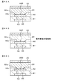
- 52A and 52B are schematic partial cross-sectional views of a conventional solid-state imaging device.
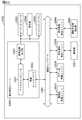
- FIG. 53 is a block diagram illustrating an example of a schematic configuration of a vehicle control system.
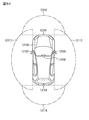
- FIG. 54 is an explanatory diagram illustrating an example of the installation positions of the outside-of-vehicle information detection unit and the imaging unit.
- FIG. 55 is a diagram illustrating an example of a schematic configuration of an endoscopic surgery system.
- FIG. 56 is a block diagram illustrating an example of a functional configuration of the camera head and the CCU.
- Embodiment 4 (Modification of Embodiments 1 to 3) 6.
- Example 5 another modification of Examples 1 to 3) 7.
- Embodiment 6 (Modification of Embodiments 4 and 5) 8.
- Embodiment 7 (Modification of Embodiments 4 to 6) 9.
- Embodiment 8 (Modification of Embodiments 4 to 7, imaging element provided with transfer control electrode) 10.
- Ninth Embodiment (Modification of Fourth to Eighth Embodiments, Image Sensor with a Plurality of Charge Storage Electrode Segments) 11.
- Embodiment 10 (Modifications of Embodiments 4 to 9, imaging elements of first and sixth configurations) 12.
- Example 11 Imaging elements of second and sixth configurations of the present disclosure) 13.
- Example 12 (third configuration imaging device) 14.
- Example 13 (fourth configuration image sensor) 15.
- Example 14 (fifth configuration image sensor) 16.
- Example 15 (image sensor of sixth configuration) 17.
- Example 16 (the solid-state imaging device according to the first embodiment of the present disclosure) 18.
- the solid-state imaging device In the solid-state imaging device according to the second embodiment of the present disclosure, at least one layer of a lower imaging element block is provided below the plurality of imaging element blocks,
- the lower image sensor block is composed of a plurality of (specifically, P P along the first direction and Q P ⁇ Q along the second direction) image sensors,
- the wavelength of the light received by the image sensor constituting the image sensor block may be different from the wavelength of the light received by the image sensor constituting the lower image sensor block.
- the lower imaging element block may be provided in two layers.
- a plurality of (specifically, P ⁇ Q) imaging elements constituting the lower imaging element block are shared. It can be configured to have a floating diffusion layer formed.
- the solid-state imaging device according to the second embodiment of the present disclosure including the preferred embodiments described above, or the solid-state imaging device according to the first embodiment of the present disclosure (hereinafter, these solid-state imaging devices are collectively referred to as For convenience, this is referred to as “the solid-state imaging device or the like of the present disclosure”), under the control of the second charge transfer control electrode, is stored in the photoelectric conversion layer between the imaging devices between adjacent imaging device blocks. The movement of the charge may be prohibited.
- the imaging device further includes a first electrode and a second electrode,
- the photoelectric conversion unit is configured by stacking a first electrode, a photoelectric conversion layer, and a second electrode,
- the charge storage electrode is disposed separately from the first electrode, and is disposed to face the photoelectric conversion layer with an insulating layer interposed therebetween.
- the first electrodes of the Q image pickup devices constituting the P-th image pickup device can be shared.
- Each image sensor block has a control unit,
- the control unit includes at least a floating diffusion layer and an amplification transistor,
- the shared first electrode can be configured to be connected to the control unit.
- the plurality of imaging element blocks are arranged in a two-dimensional matrix in a first direction and a second direction different from the first direction.
- the second charge transfer control electrode includes a second 2-A charge transfer control electrode located between image pickup devices constituting adjacent image pickup device blocks along the first direction, Under the control of the 2-A charge transfer control electrode, transfer of charges accumulated in the photoelectric conversion layer between image pickup devices between image pickup device blocks adjacent to each other along the first direction is prohibited. be able to. Note that such a configuration is referred to as a “solid-state imaging device according to a first configuration” for convenience.
- the second charge transfer control electrode includes a second-B charge transfer control electrode located between image pickup devices forming adjacent image pickup device blocks in the second direction. Under the control of the 2-B charge transfer control electrode, the transfer of the charges accumulated in the photoelectric conversion layer between the image pickup devices between the adjacent image pickup device blocks along the second direction is prohibited. be able to. Note that such a configuration is referred to as a “solid-state imaging device according to the 1-A configuration” for convenience.
- the first charge transfer control electrode is a first charge transfer control electrode located between the imaging elements adjacent to each other along the first direction in the imaging element block. It is possible to have a configuration including an -A charge transfer control electrode and a 1-B charge transfer control electrode located between the image sensors adjacent in the second direction.
- the adjacent 2-B charge transfer control electrodes are connected in adjacent image sensor blocks, and further, the 2-A charge transfer control is performed.
- a configuration in which the electrodes are connected can be employed. Note that such a configuration is referred to as a “solid-state imaging device according to the 1-B-th configuration” for convenience.
- the first charge transfer control electrode includes a first-A charge transfer control electrode located between image sensors adjacent to each other along the first direction in the image sensor block, and a first charge transfer control electrode located in the second direction. And a first-B charge transfer control electrode located between the image sensors adjacent to each other along with the first-A charge transfer control electrode and the first 1-A charge transfer control electrode.
- the -B charge transfer control electrodes may be connected.
- the adjacent 2-B charge transfer control electrode in the imaging device block, the adjacent 2-B charge transfer control electrode is connected, and further, in the adjacent imaging device block, the adjacent second-B charge transfer control electrode is connected.
- the -B charge transfer control electrodes may be connected.
- the first charge transfer control electrode includes a first-A charge transfer control electrode located between image sensors adjacent to each other along the first direction in the image sensor block, and a first charge transfer control electrode located in the second direction.
- a first-B charge transfer control electrode may be provided between adjacent image sensors along the line, and the first-B charge transfer control electrodes are connected in the image pickup device block. It can be configured.
- the first charge transfer control electrode and the second charge transfer control electrode are provided on the photoelectric conversion layer located between the adjacent image pickup devices.
- a mode can be provided in a region opposed to the region with an insulating layer interposed therebetween.
- the first charge transfer control electrode and the second charge transfer control electrode may be referred to as a “lower first charge transfer control electrode” and a “lower second charge transfer control electrode” for convenience.
- the first charge transfer control electrode and the second charge transfer control electrode may be provided on a region of the photoelectric conversion layer located between the adjacent image pickup devices and separated from the second electrode. Can be.
- the first charge transfer control electrode and the second charge transfer control electrode may be referred to as an “upper first charge transfer control electrode” and an “upper second charge transfer control electrode” for convenience.
- the imaging is performed.
- the configuration and structure in a pixel region in which a plurality of elements are arranged can be simplified and miniaturized.
- One floating diffusion layer is provided for one image sensor block composed of P ⁇ Q image sensors.
- the P ⁇ Q image sensors provided for one floating diffusion layer may be composed of a plurality of first type image sensors to be described later, or at least one first type image sensor. And one or more second-type image sensors to be described later.
- the (P-1) -th to (P-1) -th imaging elements under the control of the first charge transfer control electrode, the (P-1) -th to (P-1) -th imaging elements along the first direction.
- the charge accumulated in the photoelectric conversion layer of the imaging device of No. 1 is transferred to the photoelectric conversion layer of the P-th imaging device, and is read out together with the charge accumulated in the photoelectric conversion layer of the Q P-th imaging device.
- Such a reading method is referred to as a “first mode reading method” for convenience.
- signals obtained by four photoelectric conversion elements are added to increase the sensitivity.
- the second mode readout method can be employed in addition to the first mode readout method. Switching between the first mode readout method and the second mode readout method can be achieved by providing an appropriate switching unit in the solid-state imaging device.
- the reading method in the second mode means that the charges accumulated in the photoelectric conversion layers of the plurality of imaging elements adjacent to the first electrode shared by the plurality of imaging elements are sequentially passed through the first electrode.
- This is a method of reading data.
- P ⁇ Q imaging elements can share one floating diffusion layer by appropriately controlling the timing of the charge transfer period.
- the P ⁇ Q image sensors are operated in cooperation with each other, and are connected to a drive circuit described later as a unit of the image sensor. That is, P ⁇ Q image sensors constituting a unit of the image sensor are connected to one drive circuit. However, the control of the charge storage electrode is performed for each image sensor.
- P ⁇ Q imaging elements may share one contact hole.
- the arrangement relationship between the first electrode shared by the P ⁇ Q image sensors and the charge storage electrode of each image sensor is such that the first electrode is arranged adjacent to the charge storage electrode of each image sensor. In some cases.
- the first electrode is arranged adjacent to a part of the charge accumulation electrodes of the P ⁇ Q imaging elements, and is adjacent to the remaining charge accumulation electrodes of the P ⁇ Q imaging elements. In this case, the movement of the charge from the rest of the P ⁇ Q imaging elements to the first electrode is the same as the movement of the adjacent imaging element unit via the first electrode. Become.
- Second charge transfer period the first charge transfer period the charge accumulation period first electrode V 11 V 12 V 13 Second electrode V 21 V 22 V 23 Electrode for charge storage V 31 V 32 V 33 1st charge transfer control electrode 1st-A charge transfer control electrode V 41-A V 42-A V 43-A 1st-B charge transfer control electrode V 41-B V 42-B V 43-B Second charge transfer control electrode Second 2-A charge transfer control electrode V 51-A V 52-A V 53-A Second 2-B charge transfer control electrode V 51-B V 52-B V 53-B Transfer control electrode V 61 V 62 V 63 Charge discharging electrode V 71 V 72 V 73
- the image sensor (hereinafter, for convenience, referred to as “the image sensor in the present disclosure”) that forms the image sensor block of the solid-state imaging device or the like of the present disclosure including the above-described preferred embodiments and configurations further includes a semiconductor substrate.
- the photoelectric conversion unit may be arranged above the semiconductor substrate.
- the first electrode, the charge storage electrode, the second electrode, the first charge transfer control electrode, the second charge transfer control electrode, and the various electrodes are connected to a drive circuit described later.
- the imaging element according to the present disclosure including the various preferable modes and configurations described above is disposed between the first electrode and the charge storage electrode, and is separated from the first electrode and the charge storage electrode.
- a mode may be further provided with a transfer control electrode (charge transfer electrode) arranged to face the photoelectric conversion layer with the insulating layer interposed therebetween.
- a transfer control electrode charge transfer electrode
- the imaging device in the present disclosure which includes a transfer control electrode, the charge accumulation period, the potential applied to the transfer control electrode when the V 61, the potential of the first electrode of the second electrode
- V 61 the potential of the first electrode of the second electrode
- V 33 the potential applied to the transfer control electrode is V 63
- V 33 the potential of the first electrode is higher than the potential of the second electrode
- the charge discharging electrode connected to the photoelectric conversion layer and spaced apart from the first electrode and the charge storage electrode. May be further provided.
- the imaging element according to the embodiment of the present disclosure having such a configuration is referred to as an “imaging element according to the present disclosure including a charge discharging electrode” for convenience.
- the charge discharging electrode may be arranged so as to surround the first electrode and the charge storage electrode (that is, in a frame shape).
- the charge discharging electrode can be shared (shared) by a plurality of imaging devices.
- the first charge transfer control electrode and the second charge transfer control electrode include an upper first charge transfer control electrode and an upper second charge transfer control electrode.
- the photoelectric conversion layer extends in the second opening provided in the insulating layer, is connected to the charge discharging electrode, The edge of the top surface of the charge discharging electrode is covered with an insulating layer, A charge discharge electrode is exposed at the bottom of the second opening,
- the surface of the insulating layer in contact with the top surface of the charge discharging electrode is the third surface
- the surface of the insulating layer in contact with the portion of the photoelectric conversion layer facing the charge storage electrode is the second surface
- the side surface of the second opening is , A form having a slope that spreads from the third surface toward the second surface.
- a control unit provided on the semiconductor substrate and having a drive circuit
- the first electrode, the charge storage electrode, and the charge discharge electrode are connected to a drive circuit
- the driving circuit In the charge accumulation period, the driving circuit, the potential V 11 is applied to the first electrode, the potential V 31 is applied to the charge storage electrode, the potential V 71 is applied to the charge discharging electrodes, electric charges accumulated in the photoelectric conversion layer
- the driving circuit In the second charge transfer period, the driving circuit, the potential V 13 is applied to the first electrode, the potential V 33 is applied to the charge storage electrode, the potential V 73 is applied to the charge discharging electrode, accumulated in the photoelectric conversion layer
- the configuration may be such that the charge is read out to the control unit via the first electrode.
- the charge storage electrode may be configured to include a plurality of charge storage electrode segments.
- an image sensor according to the present disclosure of the present disclosure may be referred to as “an image sensor according to the present disclosure including a plurality of charge storage electrode segments” for convenience.
- the number of charge storage electrode segments may be two or more.
- the imaging device according to the present disclosure including the plurality of charge storage electrode segments when applying a different potential to each of the N charge storage electrode segments, When the potential of the first electrode is higher than the potential of the second electrode, the potential is applied to the charge storage electrode segment (first photoelectric conversion segment) located closest to the first electrode during the second charge transfer period.
- the potential to be applied is higher than the potential applied to the charge storage electrode segment (the Nth photoelectric conversion unit segment) located farthest from the first electrode, When the potential of the first electrode is lower than the potential of the second electrode, the potential is applied to the charge storage electrode segment (first photoelectric conversion unit segment) located closest to the first electrode during the second charge transfer period.
- the applied potential may be lower than the potential applied to the charge storage electrode segment (the N-th photoelectric conversion unit segment) located farthest from the first electrode.
- the size of the charge storage electrode may be larger than the first electrode. Assuming that the area of the charge storage electrode is s 1 ′ and the area of the first electrode is s 1 , 4 ⁇ s 1 '/ s 1 Is preferably satisfied.
- the second electrode located on the light incident side may be shared by a plurality of image sensors, except when the upper charge transfer control electrode is formed. That is, the second electrode can be a so-called solid electrode.
- the photoelectric conversion layer can be shared by a plurality of imaging devices. That is, a mode in which one photoelectric conversion layer is formed in a plurality of imaging elements can be employed.
- the first electrode extends in the opening provided in the insulating layer and is connected to the photoelectric conversion layer. can do.
- the photoelectric conversion layer can extend in the opening provided in the insulating layer and be connected to the first electrode.
- the edge of the top surface of the first electrode is covered with an insulating layer, The first electrode is exposed at the bottom of the opening, When the surface of the insulating layer in contact with the top surface of the first electrode is the first surface, and the surface of the insulating layer in contact with the portion of the photoelectric conversion layer facing the charge storage electrode is the second surface, the side surface of the opening is the second surface.
- the opening may have a slope extending from the first surface to the second surface, and the side surface of the opening having the slope extending from the first surface to the second surface may be located on the charge storage electrode side. It can be taken as a form. Note that another layer is formed between the photoelectric conversion layer and the first electrode (for example, a material layer suitable for charge storage is formed between the photoelectric conversion layer and the first electrode). Is included.
- the semiconductor substrate is provided with at least a floating diffusion layer and an amplification transistor that constitute a control unit,
- the first electrode may be connected to the floating diffusion layer and the gate of the amplification transistor.
- the semiconductor substrate is further provided with a reset transistor and a selection transistor that constitute a control unit,
- the floating diffusion layer is connected to one source / drain region of the reset transistor,
- One source / drain region of the amplification transistor may be connected to one source / drain region of the selection transistor, and the other source / drain region of the selection transistor may be connected to a signal line.
- examples of modifications of the imaging device according to the present disclosure including the various preferable modes and configurations described above include imaging devices having first to sixth configurations described below. That is, in the imaging devices of the first to sixth configurations in the imaging device of the present disclosure including the various preferable modes and configurations described above,
- the photoelectric conversion unit is composed of N (where N ⁇ 2) photoelectric conversion unit segments
- the photoelectric conversion layer is composed of N photoelectric conversion layer segments
- the insulating layer is composed of N insulating layer segments
- the charge storage electrode includes N charge storage electrode segments.
- the charge storage electrode includes N charge storage electrode segments that are spaced apart from each other.
- the photoelectric conversion unit segment having a larger value of n is located farther from the first electrode.
- the thickness of the insulating layer segment gradually changes from the first photoelectric conversion unit segment to the Nth photoelectric conversion unit segment.
- the thickness of the photoelectric conversion layer segment gradually changes from the first photoelectric conversion unit segment to the Nth photoelectric conversion unit segment.
- the material forming the insulating layer segment is different between the adjacent photoelectric conversion unit segments.
- the material forming the charge storage electrode segment is different between the adjacent photoelectric conversion unit segments.
- the area of the charge storage electrode segment gradually decreases from the first photoelectric conversion unit segment to the Nth photoelectric conversion unit segment. Note that the area may be continuously reduced or may be reduced stepwise.
- the stacking direction of the charge storage electrode, the insulating layer, and the photoelectric conversion layer is set in the Z direction, and the first electrode is stacked.
- the cross-sectional area of the laminated portion obtained by cutting the laminated portion where the charge storage electrode, the insulating layer, and the photoelectric conversion layer are laminated on the YZ virtual plane is the distance from the first electrode.
- the change in the cross-sectional area may be a continuous change or a step-like change.
- the N photoelectric conversion layer segments are provided continuously, and the N insulating layer segments are also provided continuously, and the N charge storage electrodes are provided. The segments are also provided continuously.
- the N photoelectric conversion layer segments are provided continuously.
- N insulating layer segments are provided continuously, while in the image pickup device of the third configuration, the N insulating layer segments are Is provided corresponding to each of.
- the N charge storage electrode segments are provided corresponding to each of the photoelectric conversion unit segments. I have.
- the same potential is applied to all of the charge storage electrode segments.
- different potentials may be applied to each of the N charge storage electrode segments.
- the thickness of the insulating layer segment is defined, or Further, the thickness of the photoelectric conversion layer segment is specified, or the material constituting the insulating layer segment is different, or the material constituting the charge storage electrode segment is different, or the charge storage electrode segment is different. Since the area is defined or the cross-sectional area of the laminated portion is defined, a kind of charge transfer gradient is formed, and the charge generated by photoelectric conversion can be more easily and reliably transferred to the first electrode. It becomes possible to transfer. As a result, it is possible to prevent the occurrence of an afterimage and the occurrence of a charge transfer residue.
- a solid-state imaging device including a plurality of the imaging elements having the above-described first to sixth configurations can be used.
- a solid-state imaging device including a plurality of stacked imaging devices having at least one imaging device having the above-described first to sixth configurations can be provided.
- the photoelectric conversion unit segment having a larger value of n is located farther from the first electrode, but whether or not it is farther from the first electrode is determined in the X direction.
- the direction away from the first electrode is defined as the X direction, but the “X direction” is defined as follows. That is, the pixel region in which a plurality of image sensors or stacked-type image sensors are arranged is composed of pixels arranged in a two-dimensional array, that is, regularly arranged in the X and Y directions.
- the planar shape of the pixel When the planar shape of the pixel is rectangular, the direction in which the side closest to the first electrode extends is defined as the Y direction, and the direction orthogonal to the Y direction is defined as the X direction.
- the planar shape of the pixel is an arbitrary shape, the overall direction including the line segment or curve closest to the first electrode is defined as the Y direction, and the direction orthogonal to the Y direction is defined as the X direction.
- the potential of the first electrode is higher than the potential of the second electrode
- the potential of the first electrode is lower than the potential of the second electrode.
- the level of the potential may be reversed.
- the thickness of the insulating layer segment gradually changes from the first photoelectric conversion unit segment to the Nth photoelectric conversion unit segment. May gradually become thicker or thinner, whereby a kind of charge transfer gradient is formed.
- the thickness of the insulating layer segment When the charge to be stored is electrons, the thickness of the insulating layer segment may be gradually increased, and when the charge to be stored is holes, the thickness of the insulating layer segment may be gradually increased. What is necessary is just to employ
- the thickness of the photoelectric conversion layer segment gradually changes from the first photoelectric conversion unit segment to the Nth photoelectric conversion unit segment.
- the thickness of the layer segments may be progressively thicker or thinner, which forms a kind of charge transfer gradient.
- the thickness of the photoelectric conversion layer segment When charges to be stored are electrons, the thickness of the photoelectric conversion layer segment may be gradually increased, and when charges to be stored are holes, the thickness of the photoelectric conversion layer segment may be increased. It is only necessary to adopt a configuration that gradually becomes thinner.
- the thickness of the photoelectric conversion layer segment gradually increases, when the state of V 31 ⁇ V 11 is satisfied during the charge storage period, and when the thickness of the photoelectric conversion layer segment gradually decreases, the charge storage When the state becomes V 31 ⁇ V 11 in the period, a stronger electric field is applied to the n-th photoelectric conversion unit segment than to the (n + 1) -th photoelectric conversion unit segment, and the n-th photoelectric conversion segment increases from the first photoelectric conversion segment. The flow of charges to the first electrode can be reliably prevented.
- the material forming the insulating layer segment is different in the adjacent photoelectric conversion unit segments, which forms a kind of charge transfer gradient. It is preferable that the value of the relative dielectric constant of the material forming the insulating layer segment gradually decreases from the segment to the Nth photoelectric conversion segment.
- the material forming the charge storage electrode segment is different between the adjacent photoelectric conversion unit segments, which forms a kind of charge transfer gradient. It is preferable that the work function value of the material forming the insulating layer segment gradually increases from the conversion section segment to the N-th photoelectric conversion section segment.
- the area of the charge storage electrode segment gradually decreases from the first photoelectric conversion unit segment to the Nth photoelectric conversion unit segment. Since a kind of charge transfer gradient is formed, when the state of V 31 ⁇ V 11 is satisfied during the charge accumulation period, the n-th photoelectric conversion unit segment is more than the (n + 1) -th photoelectric conversion segment. Many charges can be stored. Then, in a state of V 33 ⁇ V 13 in the second charge transfer period, the flow of charge from the first photoelectric conversion unit segment to the first electrode and the (n + 1) th photoelectric conversion unit segment to the nth The flow of electric charges to the third photoelectric conversion unit segment can be reliably ensured.
- the cross-sectional area of the stacked portion changes depending on the distance from the first electrode, thereby forming a kind of charge transfer gradient.
- the thickness of the cross section of the stacked portion is constant and the width of the cross section of the stacked portion is reduced as the distance from the first electrode is increased, as described in the imaging device of the fifth configuration, In the charge accumulation period, when a state of V 31 ⁇ V 11 is satisfied, more charge can be accumulated in a region near the first electrode than in a region far from the first electrode.
- the image pickup device of the first configuration can be used. As described above, in the state of V 31 ⁇ V 11 during the charge storage period, a region closer to the first electrode can store more charges than a region farther from the first electrode, and a strong electric field is generated.
- the flow of charges from a region near the first electrode to the first electrode can be reliably prevented.
- the second charge transfer period when the state of V 33 ⁇ V 13 is satisfied, the flow of charges from the region near the first electrode to the first electrode and the flow of charges from the region far from the region near the electrode are reliably ensured. can do.
- the charge accumulation period becomes V 31 ⁇ V 11 , A stronger electric field is applied to a region closer to the first electrode than to a region farther from the region, and the flow of charges from the region closer to the first electrode to the first electrode can be reliably prevented.
- the second charge transfer period when the state of V 33 ⁇ V 13 is satisfied, the flow of charges from the region near the first electrode to the first electrode and the flow of charges from the region far from the region near the electrode are reliably ensured. can do.
- light is incident from the second electrode side, and a light shielding layer is formed on the light incident side from the second electrode. It can be.
- light may be incident from the second electrode side, and light may not be incident on the first electrode (in some cases, the first electrode and the transfer control electrode).
- a light-shielding layer may be formed on the light incident side of the second electrode and above the first electrode (in some cases, the first electrode and the transfer control electrode).
- an on-chip micro lens is provided above the charge storage electrode and the second electrode, and light incident on the on-chip micro lens is focused on the charge storage electrode. It can be in a form.
- the light shielding layer may be provided above the light incident side surface of the second electrode, or may be provided on the light incident side surface of the second electrode. In some cases, a light shielding layer may be formed on the second electrode.
- a material forming the light-shielding layer include chromium (Cr), copper (Cu), aluminum (Al), tungsten (W), and a resin (for example, a polyimide resin) that does not transmit light.
- the imaging device is sensitive to blue light provided with a photoelectric conversion layer (for convenience, referred to as “first type blue photoelectric conversion layer”) that absorbs blue light (light of 425 nm to 495 nm).
- a photoelectric conversion layer for convenience, referred to as “first type blue photoelectric conversion layer”
- first-type blue light imaging device and a photoelectric conversion layer that absorbs green light (light of 495 nm to 570 nm)
- first-type green photoelectric conversion layer Having a sensitivity to green light
- first type image sensor for green light a photoelectric conversion layer
- a photoelectric conversion layer for convenience, absorbing light of 620 nm to 750 nm.
- An image sensor (hereinafter, referred to as a “first type red light imaging device”) having sensitivity to red light having a “first type red photoelectric conversion layer” may be used.
- a conventional image sensor having no charge storage electrode and having sensitivity to blue light is referred to as a "second type blue light image sensor” for convenience and has sensitivity to green light.
- the image sensor is referred to as a “second type green light image sensor” for convenience, and the image sensor having sensitivity to red light is referred to as a “second type red light image sensor” for convenience.
- the photoelectric conversion layer forming the blue light imaging device is referred to as a “second type blue photoelectric conversion layer” for convenience, and the photoelectric conversion layer forming the second type green light imaging device is referred to as “second type blue light conversion layer” for convenience.
- the second type red photoelectric conversion layer is referred to as a “second type red photoelectric conversion layer” for convenience.
- the stacked image sensor according to the present disclosure has at least one image sensor (photoelectric conversion element) according to the present disclosure.
- a first type of photoelectric conversion unit for blue light, a first type of photoelectric conversion unit for green light, and a first type of photoelectric conversion unit for red light are vertically stacked,
- a blue light photoelectric conversion unit of the type and a first type green light photoelectric conversion unit are vertically stacked, Below these two layers of the first type photoelectric conversion units, a second type red light photoelectric conversion unit is disposed, A configuration and a structure in which the first type of blue light image sensor, the first type of green light image sensor, and the second type of red light image sensor are provided on a semiconductor substrate, respectively. Below the type green light photoelectric conversion unit, a second type blue light photoelectric conversion unit and a second type red light photoelectric conversion unit are arranged, A configuration and a structure in which each of a control unit of a first type of green light imaging device, a second type of blue light imaging device, and a second type of red light imaging device is provided on a semiconductor substrate.
- a second type green light photoelectric conversion unit and a second type red light photoelectric conversion unit are arranged, A configuration and a structure in which the control units of the first type of blue light imaging device, the second type of green light imaging device, and the second type of red light imaging device are provided on a semiconductor substrate, respectively.
- the arrangement order of the photoelectric conversion units in the vertical direction of these imaging devices is such that the order of the photoelectric conversion unit for blue light, the photoelectric conversion unit for green light, and the photoelectric conversion unit for red light is from the light incident direction, or To green light photoelectric converter, blue light photoelectric converter, and red light photoelectric converter. This is because light having a shorter wavelength is more efficiently absorbed on the incident surface side.
- red Since red has the longest wavelength among the three colors, it is preferable to position the photoelectric conversion unit for red light in the lowermost layer when viewed from the light incident surface.
- One pixel is constituted by the laminated structure of these imaging elements.
- a first type infrared photoelectric conversion unit may be provided.
- the photoelectric conversion layer of the first type infrared photoelectric conversion unit is made of, for example, an organic material, is the lowermost layer of the stacked structure of the first type imaging device, and is lower than the second type imaging device. It is also preferable to arrange them above.
- a second type infrared photoelectric conversion unit may be provided below the first type photoelectric conversion unit.
- the first electrode is formed on an interlayer insulating layer provided on a semiconductor substrate.
- the imaging element formed on the semiconductor substrate can be of a back-illuminated type or a front-illuminated type.
- the photoelectric conversion layer When the photoelectric conversion layer is composed of an organic material, the photoelectric conversion layer (1) It is composed of a p-type organic semiconductor. (2) It is composed of an n-type organic semiconductor. (3) It has a laminated structure of p-type organic semiconductor layer / n-type organic semiconductor layer. It has a laminated structure of a p-type organic semiconductor layer / a mixed layer of p-type organic semiconductor and n-type organic semiconductor (bulk heterostructure) / n-type organic semiconductor layer. It has a laminated structure of a p-type organic semiconductor layer / a mixed layer (bulk heterostructure) of a p-type organic semiconductor and an n-type organic semiconductor.
- n-type organic semiconductor layer / a mixed layer (bulk heterostructure) of a p-type organic semiconductor and an n-type organic semiconductor.
- fullerenes and fullerene derivatives eg, fullerenes (higher order fullerenes such as C60, C70, C74, etc., endohedral fullerenes, etc.) or fullerene derivatives (eg, fullerene fluorides, PCBM fullerene compounds, fullerene multimers, etc.)
- fullerenes and fullerene derivatives eg, fullerene fluorides, PCBM fullerene compounds, fullerene multimers, etc.
- a heterocyclic compound containing a nitrogen atom, an oxygen atom, and a sulfur atom for example, a pyridine derivative, a pyrazine derivative, a pyrimidine derivative, a triazine derivative, a quinoline derivative, a quinoxaline derivative, an isoquinoline derivative, an acridine Derivatives, phenazine derivatives, phenanthroline derivatives, tetrazole derivatives, pyrazole derivatives, imidazole derivatives, thiazole derivatives, oxazole derivatives, imidazole derivatives, benzimidazole derivatives, benzotriazole derivatives, benzoxazole derivatives, benzoxazole derivatives, carbazole derivatives, benzofuran derivatives, dibenzofuran derivatives , Subporphyrazine derivatives, polyphenylenevinylene derivatives, polybenzothiadiazole derivatives, polyfluorene
- Examples of the group contained in the fullerene derivative include a halogen atom; a linear, branched, or cyclic alkyl group or a phenyl group; a group having a linear or condensed aromatic compound; a group having a halide; a partial fluoroalkyl group; Aryl group; arylsulfanyl group; alkylsulfanyl group; arylsulfonyl group; alkylsulfonyl group; arylsulfide group; alkylsulfide group; amino group; alkylamino group; arylamino group; A hydroxy group; an alkoxy group; an acylamino group; an acyloxy group; a carbonyl group; a carboxy group; a carboxamide group; a carboalkoxy group; an acyl group; a sulfonyl group; a cyano group; a nitro group; Fin group; phosphonic group
- the thickness of the photoelectric conversion layer (sometimes referred to as “organic photoelectric conversion layer”) made of an organic material is not limited, but is, for example, 1 ⁇ 10 ⁇ 8 m to 5 ⁇ 10 ⁇ 7 m. , Preferably 2.5 ⁇ 10 ⁇ 8 m to 3 ⁇ 10 ⁇ 7 m, more preferably 2.5 ⁇ 10 ⁇ 8 m to 2 ⁇ 10 ⁇ 7 m, and still more preferably 1 ⁇ 10 ⁇ 7 m to 1. 8 ⁇ 10 ⁇ 7 m can be exemplified. Note that organic semiconductors are often classified as p-type and n-type.
- the p-type means that holes can be easily transported
- the n-type means that electrons can be easily transported
- the inorganic semiconductor is inorganic. It is not limited to the interpretation that the semiconductor has holes or electrons as majority carriers of thermal excitation like a semiconductor.
- examples of the material constituting the organic photoelectric conversion layer that performs green light photoelectric conversion include, for example, rhodamine-based dyes, melacyanine-based dyes, quinacridone derivatives, subphthalocyanine-based dyes (subphthalocyanine derivatives), and blue.
- examples of a material constituting the organic photoelectric conversion layer that photoelectrically converts light include a coumaric acid dye, tris-8-hydroxyquinolialuminum (Alq3), a melanocyanine-based dye, and the like.
- Examples of the material constituting the organic photoelectric conversion layer include a phthalocyanine dye and a subphthalocyanine dye (subphthalocyanine derivative).
- crystalline silicon, amorphous silicon, microcrystalline silicon, crystalline selenium, amorphous selenium, and chalcopyrite-based compounds CIGS (CuInGaSe), CIS (CuInSe 2 ), CuInS 2 , CuAlS 2 , CuAlSe 2 , CuGaS 2 , CuGaSe 2 , AgAlS 2 , AgAlSe 2 , AgInS 2 , AgInSe 2 , or GaAs, InP, AlGaAs, InGaP, AlGaInP, and InGaAsP, which are III-V compounds.
- Compound semiconductors such as CdSe, CdS, In 2 Se 3 , In 2 S 3 , Bi 2 Se 3 , Bi 2 S 3 , ZnSe, ZnS, PbSe, and PbS can be given.
- quantum dots made of these materials can be used for the photoelectric conversion layer.
- the photoelectric conversion layer can have a stacked structure of a lower semiconductor layer and an upper photoelectric conversion layer.
- the efficiency of transferring charges accumulated in the photoelectric conversion layer to the first electrode can be increased.
- electric charges generated in the photoelectric conversion layer can be temporarily held, and transfer timing and the like can be controlled. Further, generation of dark current can be suppressed.
- the material constituting the upper photoelectric conversion layer may be appropriately selected from the various materials constituting the above photoelectric conversion layer.
- a material forming the lower semiconductor layer a material having a large band gap energy (for example, a band gap energy of 3.0 eV or more) and having a higher mobility than the material forming the photoelectric conversion layer is used. It is preferable to use Specific examples include oxide semiconductor materials; transition metal dichalcogenides; silicon carbide; diamond; graphene; carbon nanotubes; and organic semiconductor materials such as condensed polycyclic hydrocarbon compounds and condensed heterocyclic compounds.
- oxide semiconductor materials indium oxide, gallium oxide, zinc oxide, tin oxide, materials containing at least one of these oxides, materials obtained by adding a dopant to these materials
- the, for example, IGZO, ITZO, IWZO, IWO , ZTO, ITO-SiO X materials, GZO, IGO, ZnSnO 3, AlZnO, GaZnO can be exemplified InZnO, also, CuI, InSbO 4, ZnMgO, CuInO 2, MgIn 2 O 4, Ageruko a material containing CdO etc. Although it is not intended to limit to these materials.
- the electric charge to be accumulated is an electron as a material constituting the lower semiconductor layer
- a material having an ionization potential higher than the ionization potential of the material constituting the photoelectric conversion layer can be used.
- the charge is a hole
- a material having an electron affinity lower than the electron affinity of the material forming the photoelectric conversion layer can be given.
- the impurity concentration in the material forming the lower semiconductor layer is preferably 1 ⁇ 10 18 cm ⁇ 3 or less.
- the lower semiconductor layer may have a single-layer structure or a multilayer structure. Further, the material forming the lower semiconductor layer located above the charge storage electrode may be different from the material forming the lower semiconductor layer located above the first electrode.
- a single-chip color solid-state imaging device can be configured by the solid-state imaging devices according to the first and second embodiments of the present disclosure.
- the solid-state imaging device including the stacked-type imaging device is different from the solid-state imaging device including the Bayer array imaging device (that is, blue, green, and red using a color filter). Is not performed), but one pixel is formed by stacking image pickup devices having sensitivity to light of a plurality of wavelengths in the incident direction of light in the same pixel, so that the sensitivity is improved and the unit is improved.
- the pixel density per volume can be improved.
- the organic material has a high absorption coefficient, the thickness of the organic photoelectric conversion layer can be made smaller than that of the conventional Si-based photoelectric conversion layer, and light leakage from an adjacent pixel and light incident angle can be reduced. Restrictions are relaxed.
- a false color occurs because color signals are created by performing interpolation between pixels of three colors.
- the second embodiment of the present disclosure including the stacked-type image sensor.
- generation of false colors is suppressed. Since the organic photoelectric conversion layer itself also functions as a color filter, color separation is possible without providing a color filter.
- the solid-state imaging device by using the color filter, the demand for the spectral characteristics of blue, green, and red can be eased, and high productivity can be achieved. Having.
- an arrangement of the imaging elements in the solid-state imaging device according to the first embodiment of the present disclosure in addition to a Bayer arrangement, an interline arrangement, a G stripe RB checkerboard arrangement, a G stripe RB complete checkerboard arrangement, a checkerboard complementary color arrangement, a stripe arrangement, an oblique stripe Examples include an array, a primary color difference array, a field color difference sequential array, a frame color difference sequential array, a MOS type array, an improved MOS type array, a frame interleave array, and a field interleave array.
- one pixel (or sub-pixel) is constituted by one image sensor.
- a pixel region in which a plurality of image sensors according to the present disclosure or a plurality of stacked image sensors according to the present disclosure are arranged includes a plurality of pixels regularly arranged in a two-dimensional array.
- the pixel area is usually composed of an effective pixel area that actually receives light and amplifies signal charges generated by photoelectric conversion and reads it out to a drive circuit, and a black reference pixel for outputting optical black serving as a black level reference. And an area.
- the black reference pixel area is usually arranged on the outer periphery of the effective pixel area.
- the imaging device including the various preferable embodiments and configurations described above, light is irradiated, photoelectric conversion occurs in the photoelectric conversion layer, and carriers are separated from holes.
- the electrode from which holes are extracted is defined as an anode, and the electrode from which electrons are extracted is defined as a cathode.
- the first electrode forms the anode and the second electrode forms the cathode, and conversely, a form in which the first electrode forms the cathode and the second electrode forms the anode.
- the first electrode, the charge storage electrode, the first charge transfer control electrode, the second charge transfer control electrode, the transfer control electrode, and the second electrode are made of a transparent conductive material.
- the first electrode, the charge storage electrode, the first charge transfer control electrode, the second charge transfer control electrode, and the transfer control electrode may be collectively referred to as a “first electrode or the like”.
- the charge storage electrode can be made of a metal material.
- the photoelectric conversion layer is located on the incident side, and the charge storage electrode can be made of a metal or an alloy.
- an electrode made of a transparent conductive material may be referred to as a “transparent electrode”.
- the band gap energy of the transparent conductive material is desirably 2.5 eV or more, preferably 3.1 eV or more.
- the transparent conductive material constituting the transparent electrode include a conductive metal oxide. Specifically, indium oxide, indium-tin oxide (ITO, Indium Tin Oxide, Sn-doped In 2 O 3) , Crystalline ITO and amorphous ITO), indium-zinc oxide (IZO) obtained by adding indium to zinc oxide as a dopant, and indium-gallium oxide (IGO) obtained by adding indium to gallium oxide as a dopant.
- ITO indium-tin oxide
- IGO indium-gallium oxide
- Indium-gallium-zinc oxide obtained by adding indium and gallium as dopants to zinc oxide
- indium-tin-zinc oxide obtained by adding indium and tin as dopants to zinc oxide
- IFO F-doped in 2 O 3
- tin oxide SnO 2
- O SnO 2 and Sb-doped
- FTO SnO 2 of F-doped
- aluminum was added aluminum as a dopant to zinc oxide - zinc oxide (AZO), oxide Gallium-zinc oxide (GZO) in which gallium is added as a dopant to zinc
- titanium oxide TiO 2
- niobium-titanium oxide TNO
- a transparent electrode having a base layer of gallium oxide, titanium oxide, niobium oxide, nickel oxide, or the like can be given.
- the thickness of the transparent electrode may be 2 ⁇ 10 ⁇ 8 m to 2 ⁇ 10 ⁇ 7 m, preferably 3 ⁇ 10 ⁇ 8 m to 1 ⁇ 10 ⁇ 7 m.
- the other electrodes are preferably made of a transparent conductive material from the viewpoint of simplifying the manufacturing process.
- Alkali metals eg, Li, Na, K, etc.
- alkaline earth metals eg, Mg, Ca, etc.
- Alkali metals eg, Li, Na, K, etc.
- alkaline earth metals eg, Mg, Ca, etc.
- Alkali metals eg, Li, Na, K, etc.
- alkaline earth metals eg, Mg, Ca, etc.
- Alkali metals eg, Li, Na, K, etc.
- alkaline earth metals eg, Mg, Ca, etc.
- Alkali metals eg, Li, Na, K, etc.
- alkaline earth metals eg, Mg, Ca, etc.
- Alkali metals eg, Li, Na, K, etc.
- alkaline earth metals eg, Mg, Ca, etc.
- Alkali metals eg, Alkaline earth metals
- Alkaline earth metals eg
- platinum platinum (Pt), gold (Au), palladium (Pd), chromium (Cr), nickel (Ni), aluminum (Al), silver (Ag), tantalum (Ta) ), Tungsten (W), copper (Cu), titanium (Ti), indium (In), tin (Sn), iron (Fe), cobalt (Co), molybdenum (Mo), and the like, or a metal thereof.
- Alloys containing elements conductive particles made of these metals, conductive particles of alloys containing these metals, polysilicon containing impurities, carbon-based materials, oxide semiconductors, carbon nanotubes, graphene, etc. Materials, or a layered structure of layers containing these elements.
- an organic material such as poly (3,4-ethylenedioxythiophene) / polystyrenesulfonic acid [PEDOT / PSS] can be used.
- these conductive materials may be mixed with a binder (polymer) to cure a paste or ink and then used as an electrode.
- a dry method or a wet method can be used as a method for forming the first electrode and the like and the second electrode (anode and cathode).
- Examples of the dry method include physical vapor deposition (PVD) and chemical vapor deposition (CVD).
- a vacuum evaporation method using resistance heating or high frequency heating an EB (electron beam) evaporation method, various sputtering methods (magnetron sputtering method, RF-DC combined bias sputtering method, ECR Sputtering method, facing target sputtering method, high frequency sputtering method), ion plating method, laser ablation method, molecular beam epitaxy method, and laser transfer method.
- the CVD method include a plasma CVD method, a thermal CVD method, an organic metal (MO) CVD method, and a photo CVD method.
- electrolytic plating electroless plating, spin coating, ink jet, spray coating, stamping, micro contact printing, flexographic printing, offset printing, gravure printing, dipping, etc.
- the patterning method include chemical etching such as shadow mask, laser transfer, and photolithography, and physical etching using ultraviolet light, laser, or the like.
- a laser planarization method, a reflow method, a CMP (Chemical Mechanical Polishing) method, or the like can be used as a technique for planarizing the first electrode or the like or the second electrode.
- Inorganic insulating materials exemplified by metal oxide high-dielectric insulating materials such as silicon oxide-based materials; silicon nitride (SiN Y ); and aluminum oxide (Al 2 O 3 ) as materials constituting various interlayer insulating layers and insulating films.
- metal oxide high-dielectric insulating materials such as silicon oxide-based materials; silicon nitride (SiN Y ); and aluminum oxide (Al 2 O 3 ) as materials constituting various interlayer insulating layers and insulating films.
- PMMA polymethyl methacrylate
- PVP polyvinyl phenol
- PVA polyvinyl alcohol
- PC polyethylene terephthalate
- PES polystyrene
- silane coupling agents such as methoxysilane (AEAPTMS), 3-
- silicon oxide-based materials silicon oxide (SiO x ), BPSG, PSG, BSG, AsSG, PbSG, silicon oxynitride (SiON), SOG (spin-on-glass), low dielectric constant materials (for example, polyaryl ether, cycloalkyl Perfluorocarbon polymer and benzocyclobutene, cyclic fluororesin, polytetrafluoroethylene, fluorinated aryl ether, fluorinated polyimide, amorphous carbon, organic SOG) can be exemplified.
- the configuration and structure of the floating diffusion layer, the amplification transistor, the reset transistor, and the selection transistor that constitute the control unit can be the same as those of the conventional floating diffusion layer, the amplification transistor, the reset transistor, and the selection transistor.
- the drive circuit can also have a known configuration and structure.
- the first electrode is connected to the floating diffusion layer and the gate portion of the amplification transistor, but a contact hole may be formed to connect the first electrode to the floating diffusion layer and the gate portion of the amplification transistor.
- the material constituting the contact hole portion include polysilicon doped with impurities, high melting point metal such as tungsten, Ti, Pt, Pd, Cu, TiW, TiN, TiNW, WSi 2 , and MoSi 2, and metal silicide.
- a laminated structure of layers made of a material (for example, Ti / TiN / W) can be exemplified.
- a first carrier blocking layer may be provided between the organic photoelectric conversion layer and the first electrode, or a second carrier blocking layer may be provided between the organic photoelectric conversion layer and the second electrode. Further, a first charge injection layer may be provided between the first carrier blocking layer and the first electrode, or a second charge injection layer may be provided between the second carrier blocking layer and the second electrode.
- an alkali metal such as lithium (Li), sodium (Na), and potassium (K) and a fluoride or oxide thereof, or an alkaline earth such as magnesium (Mg) or calcium (Ca) are used. Metals and their fluorides and oxides can be mentioned.
- Examples of the method for forming various organic layers include a dry film formation method and a wet film formation method.
- dry film forming methods include vacuum evaporation using resistance heating or high-frequency heating, electron beam heating, flash evaporation, plasma evaporation, EB evaporation, and various sputtering methods (two-pole sputtering, DC sputtering, DC magnetron sputtering).
- Sea method MBE method
- Examples of the CVD method include a plasma CVD method, a thermal CVD method, an MOCVD method, and a photo CVD method.
- specific examples of the wet method include spin coating; dipping; casting; microcontact printing; drop casting; screen printing, ink jet printing, offset printing, gravure printing, and flexographic printing.
- Various printing methods Stamp method; Spray method; Air doctor coater method, blade coater method, rod coater method, knife coater method, squeeze coater method, reverse roll coater method, transfer roll coater method, gravure coater method, kiss coater method, cast coater
- Various coating methods such as a spray coating method, a spray coater method, a slit orifice coater method, and a calendar coater method can be exemplified.
- non-polar or low-polarity organic solvents such as toluene, chloroform, hexane, and ethanol can be exemplified as the solvent.
- the patterning method include chemical etching such as shadow mask, laser transfer, and photolithography, and physical etching using ultraviolet light or laser.
- a flattening technique for various organic layers a laser flattening method, a reflow method, or the like can be used.
- the imaging element or the solid-state imaging device may be provided with an on-chip micro lens or a light-shielding layer as necessary, or provided with a driving circuit or wiring for driving the imaging element. . If necessary, a shutter for controlling the incidence of light on the imaging device may be provided, or an optical cut filter may be provided according to the purpose of the solid-state imaging device.
- a solid-state imaging device is stacked with a readout integrated circuit (ROIC)
- a drive substrate on which a connection portion made of a readout integrated circuit and copper (Cu) is formed, and an image pickup device on which a connection portion is formed are formed.
- the connection portions By stacking the connection portions so that the connection portions are in contact with each other and joining the connection portions, the layers can be laminated, and the connection portions can be joined using solder bumps or the like.
- the electric charge in the first electrode is discharged out of the system while simultaneously accumulating the electric charge in the photoelectric conversion layer.
- the charges accumulated in the photoelectric conversion layer are simultaneously transferred to the first electrode, and after the transfer is completed, the charges transferred to the first electrode in each image sensor are sequentially read out.
- a method for driving a solid-state imaging device that repeats each step can be provided.
- each imaging device has a structure in which light incident from the second electrode side does not enter the first electrode, and all the imaging devices simultaneously perform photoelectric conversion. Since the electric charge in the first electrode is discharged out of the system while accumulating the electric charge in the conversion layer, it is possible to surely reset the first electrode in all the imaging elements at the same time. Then, in all the image sensors, the charges accumulated in the photoelectric conversion layer are simultaneously transferred to the first electrode, and after the transfer is completed, the charges transferred to the first electrode in each image sensor are sequentially read. Therefore, a so-called global shutter function can be easily realized.
- Example 1 relates to the solid-state imaging device according to the first embodiment and the second embodiment of the present disclosure, and specifically, the solid-state imaging device according to the first configuration, and the solid-state imaging device according to the first-A configuration.
- FIG. 1 schematically illustrates an arrangement state of an imaging element block, a charge storage electrode, a first charge transfer control electrode, a second charge transfer control electrode, and a first electrode in the solid-state imaging device according to the first embodiment.
- FIG. 2 schematically shows the arrangement of the image sensor block and the two layers of lower image sensor blocks.
- various imaging element components located below the interlayer insulating layer 81 described below may be collectively indicated by reference numeral 91 for convenience in order to simplify the drawing.
- a first charge transfer control electrode 31 is provided between the image pickup device 11 and the image pickup device 11
- a second charge transfer control electrode 32 is provided between the image sensor block 10 and the image sensor block 10
- P imaging devices 11 are arranged along a first direction
- Q imaging devices 11 are arranged along a second direction different from the first direction.
- the charges accumulated in the photoelectric conversion layer 23 of the (P-1) -th image sensor 11 from the first image sensor 11 along the first direction are transferred to the photoelectric conversion layer 23 of the P-th imaging element 11 and together with the electric charges accumulated in the photoelectric conversion layers 23 of the Q P-th imaging elements 11. Is read. Further, under the control of the second charge transfer control electrode 32, transfer of charges accumulated in the photoelectric conversion layer 23 between the image pickup devices 11 between adjacent image pickup device blocks is prohibited.
- the solid-state imaging device includes the stacked imaging device including at least one imaging device according to the first embodiment.
- the imaging element block 10 includes four imaging elements 11 having charge storage electrodes 24 11 , 24 12 , 24 21 , and 24 22 , and the first electrode 21 11 is shared. Further, the image pickup device block 10 is configured by four image pickup devices 11 having the charge storage electrodes 24 13 , 24 14 , 24 23 , and 24 24 , and the first electrode 21 13 is shared. Similarly, the image pickup device block 10 includes four image pickup devices 11 having charge storage electrodes 24 31 , 24 32 , 24 41 , and 24 42 , the first electrode 21 31 is shared, and the charge storage electrodes 24 33 , The imaging element block 10 is configured by four imaging elements 11 having 24 34 , 24 43 , and 24 44 , and the first electrode 2133 is shared.
- One image sensor block 10 is constituted by four image sensors 11 having charge storage electrodes 24 11 , 24 12 , 24 21 , and 24 22 , and the first electrode 21 11 is shared. explain. Under the control of the first charge transfer control electrode 31, the charge accumulated in the first image sensor 11 11 along the first direction is changed to the P-th (specifically, the second) image sensor 11 11 It is transferred to 12 photoelectric conversion layers 23. Similarly, the charge accumulated in the first-th image pickup element 11 21 (specifically, the second) the P th is transferred to the photoelectric conversion layer 23 of the image sensor 11 22.
- At least one lower layer (two layers in the first embodiment) of lower image sensor blocks 12 and 14 is provided below the plurality of image sensor blocks 10.
- the number of the image pickup device blocks 12 and 14 is plural (specifically, P ⁇ Q in the first direction and Q ⁇ P ⁇ Q in the second direction, more specifically, 2 ⁇ P ⁇ Q).
- the imaging elements 11 p, q (in the illustrated example, p is an integer of 1 to 4, and q is also 1 to 4). (Integer) is different from the wavelength of light received by the image sensors 13 p, q , 15 p, q constituting the lower image sensor blocks 12 and 14.
- a plurality of (specifically, P ⁇ Q) image sensors 13 p, q , 15 p, q constituting the lower image sensor blocks 12 and 14 are shared by the floating diffusion layer FD. and a 2, FD 3.
- a gate section connecting the image pickup devices 13 p, q , 15 p, q and the drive circuit is indicated by reference numeral 16 which is schematically enclosed by a circle.
- the image sensor 11, the image sensor 13, and the image sensor 15 at least partially overlap each other.
- the size of the photoelectric conversion unit forming the imaging device 11, the size of the photoelectric conversion unit forming the imaging device 13, and the size of the photoelectric conversion unit forming the imaging device 15 may be the same or different.
- one pixel includes, for example, the imaging elements 11 11 , 11 12 , 11 21 , and 11 22 , and the imaging elements 13 11 , 13 12 , and 13. 21 , 13 22 , and imaging elements 15 11 , 15 12 , 15 21 , 15 22 .
- one pixel is composed of, for example, from the imaging element 11 11, the image pickup device 13 11 and the image pickup element 15 11
- the imaging device 11 12, image pickup device 13 consist 12 and the imaging element 15 12
- the imaging device 11 21 is composed of the image pickup device 13 21 and the image pickup device 15 21, or alternatively, consist of the imaging element 11 22, the imaging element 13 22 and the image sensor 15 22 Is done.
- the imaging device constituting the solid-state imaging device will be described in detail in Embodiment 4 and later. It further includes an imaging element 11, a first electrode 21, and a second electrode 22,
- the photoelectric conversion unit is configured by stacking a first electrode 21, a photoelectric conversion layer 23, and a second electrode 22,
- the charge storage electrode 24 is disposed apart from the first electrode 21, and is disposed to face the photoelectric conversion layer 23 via the insulating layer 82.
- the first electrodes 21 of the Q image sensors 11 constituting the P-th image sensor 11 are shared.
- Each imaging element block 10 has a control unit (details will be described later), and the control unit includes at least a floating diffusion layer and an amplification transistor. Connected to the unit.
- the plurality of imaging element blocks 10 are arranged in a two-dimensional matrix in a first direction and a second direction different from the first direction.
- the second charge transfer control electrode 32 includes a second 2-A charge transfer control electrode 32A located between the image sensors 11 constituting the adjacent image sensor blocks 10 along the first direction, Under the control of the 2-A charge transfer control electrode 32A, transfer of charges accumulated in the photoelectric conversion layer 23 between the image pickup devices 11 between the image pickup device blocks adjacent in the first direction is prohibited. .
- the second charge transfer control electrode includes a second-B charge transfer control electrode 32B located between the image sensors 11 constituting the adjacent image sensor blocks 10 along the second direction, Under the control of the second-B charge transfer control electrode 32B, transfer of charges accumulated in the photoelectric conversion layer 23 between the image pickup elements 11 between the adjacent image pickup element blocks along the second direction is prohibited.
- the first charge transfer control electrode 31 is a first-A charge transfer control electrode 31A located between the adjacent image pickup devices 11 along the first direction in the image pickup device block 10, and And a first-B charge transfer control electrode 31B located between the imaging elements 11 adjacent to each other along the second direction.
- the first charge transfer control electrode 31 and the second charge transfer control electrode 32 face each other with the insulating layer 82 interposed between the photoelectric conversion layers 23 located between the adjacent imaging elements 11.
- the first charge transfer control electrode 31 and the second charge transfer control electrode 32 are a lower first charge transfer control electrode and a lower second charge transfer control electrode.
- the first charge transfer control electrode 31 and the second charge transfer control electrode 32 may be formed at the same level as the first electrode 21 or the charge storage electrode 24, or may be formed at different levels.
- a control unit provided on the semiconductor substrate and having a driving circuit is further provided, and the first electrode 21, the second electrode 22, the charge storage electrode 24, the first charge transfer control electrode 31, and the second charge transfer control are provided.
- the electrode 32 is connected to a drive circuit.
- the first electrode 21 when the first electrode 21 is set to a positive potential and the second electrode 22 is set to a negative potential, electrons generated by photoelectric conversion in the photoelectric conversion layer 23 are read out to the floating diffusion layer.
- the second electrode 22 in a mode in which the first electrode 21 is set to a negative potential, the second electrode 22 is set to a positive potential, and holes generated based on photoelectric conversion in the photoelectric conversion layer 23 are read out to the floating diffusion layer, The level of the potential described above may be reversed.
- the reading method is a reading method in the first mode.
- signals obtained by the four photoelectric conversion elements 11 constituting the imaging element block 10 are added to increase the sensitivity.
- 3A, 4A, 5A, and 6A show the potential of each electrode along the two-dot chain line AAA shown in FIG. 1, and FIGS. 3B, 4B, 5B, and 6B. 1 shows the potential of each electrode along the one-dot chain line BB shown in FIG. 1.
- FIGS. 3C, 4C, 5C and 6C show the potentials of the respective electrodes along the one-dot chain line CC shown in FIG. The potential of each electrode along is shown. In these drawings, the potential is indicated by the height in the vertical direction, and the lower the height, the higher the potential.
- the drive circuit applies the potential V 11 to the first electrode 21 and the potential V 31 to the charge storage electrode 24.
- the potential V 41-a is applied to the 1-a charge transfer control electrode 31A
- the potential V 41-B is applied to the 1-B charge transfer control electrode 31B
- the 2-a charge transfer control electrode 32A potential V 51-a is applied
- the potential V 51-B is applied to the 2-B charge transfer control electrodes 32B to.
- a potential V 21 is applied to the second electrode 22.
- charges (electrons, schematically indicated by black dots) are accumulated in the photoelectric conversion layer 23.
- the potentials have the relationship shown in Table 2-A below.
- FIGS. 3A, 3B and 3C schematically show the charge accumulation state immediately before the end of the charge accumulation period.
- the electrons generated by the photoelectric conversion are attracted to the charge storage electrode 24 and stop in a region of the photoelectric conversion layer 23 facing the charge storage electrode 24. That is, charges are accumulated in the photoelectric conversion layer 23.
- the potential of the region of the photoelectric conversion layer 23 located above the region between the first electrode 21 and the charge storage electrode 24 is the potential formed by the first electrode 21 and the charge storage electrode 24. is lower than V 31, electrons generated within the photoelectric conversion layer 23, does not move toward the first electrode 21.
- the potential of the charge storage electrode 24 is higher than the potentials of the first charge transfer control electrode 31 and the second charge transfer control electrode 32, the electrons generated inside the photoelectric conversion layer 23 generate the first charge transfer control. There is no movement toward the electrode 31 and the second charge transfer control electrode 32. That is, it is possible to suppress the charge generated by the photoelectric conversion from flowing into the adjacent image sensor.
- the photoelectric conversion time elapses, the potential in the region of the photoelectric conversion layer 23 facing the charge storage electrode 24 becomes a more negative value. In the latter half of the charge accumulation period, a reset operation is performed. Accordingly, the first potential of the floating diffusion layer FD 1 is reset, the potential of the first floating diffusion layer FD 1 becomes the power supply potential V DD.
- the first charge transfer period After the completion of the reset operation, the first charge transfer period starts.
- the drive circuit applies the potential V 12 to the first electrode 21, applies the potentials V 32 and V 32 ′ to the charge storage electrode 24, and sets the 1-A charge transfer control electrode 31A.
- potential V 42-a is applied
- the potential V 42-B is applied to the 1-B charge transfer control electrode 31B
- the potential V 52-a is applied to the 2-a charge transfer control electrode 32A
- the second The potential V52 -B is applied to the -B charge transfer control electrode 32B.
- a potential V 22 is applied to the second electrode 22.
- the charges accumulated in the photoelectric conversion layer 23 of the (P-1) -th imaging element 11 from the first imaging element 11 along the first direction are converted by the photoelectric conversion of the P-th imaging element 11. Transferred to layer 23.
- the potential immediately after the start of the first charge transfer period and the potential immediately before the end of the first charge transfer period have a relationship shown in Table 2-B below.
- the potential V 32 is applied to the charge storage electrode 24 located closer to the second electrode 21 as a reference, and the potential V 32 ′ (is applied to the charge storage electrode 24 located farther from the second electrode 21 as a reference. ⁇ V 32 ) is applied.
- 4A, 4B, and 4C schematically show the charge accumulation state immediately after the start of the first charge transfer period, and FIGS.
- FIG. 5A and 5B schematically show the charge accumulation state immediately before the end of the first charge transfer period. And FIG. 5C.
- the potential of the region of the photoelectric conversion layer 23 located above the region between the first electrode 21 and the charge storage electrode 24 is the potential formed by the first electrode 21 and the charge storage electrode 24, Since it is lower than V 32 , electrons generated inside the photoelectric conversion layer 23 do not move toward the first electrode 21.
- the drive circuit applies the potential V 13 to the first electrode 21, and applies the potentials V 33 and V 33 ′ (or V 33 ) to the charge storage electrode 24.
- potential V 43-a to a charge transfer control electrode 31A is applied
- the potential V 43-B is applied to the 1-B charge transfer control electrode 31B
- the potential V 53-B is applied to the second-B charge transfer control electrode 32B.
- the potential V 23 is applied to the second electrode 22. In this manner, the charges transferred to the photoelectric conversion layer 23 of the P-th imaging element 11 are read out together with the charges accumulated in the photoelectric conversion layers 23 of the Q P-th imaging elements 11.
- FIGS. 6A, 6B, and 6C schematically show the charge accumulation state in the second charge transfer period.
- the potential of the region of the photoelectric conversion layer 23 located above the region between the first electrode 21 and the charge storage electrode 24 is the potential formed by the first electrode 21 and the charge storage electrode 24, is higher than V 33, the electrons are stopped in the region of the photoelectric conversion layer 23 opposed to the charge storage electrode 24, first electrode 21, furthermore, it is read into the first floating diffusion layer FD 1. In other words, the charges stored in the photoelectric conversion layer 23 are read out to the control unit.
- the potential of the charge storage electrode 24 is higher than the potentials of the first charge transfer control electrode 31 and the second charge transfer control electrode 32, the electrons generated inside the photoelectric conversion layer 23 are subjected to the first charge transfer control. It does not move toward the electrode 31 and the second charge transfer control electrode 32. That is, it is possible to suppress the charge generated by the photoelectric conversion from flowing into the adjacent image sensor.
- Switching between the first mode readout method and the second mode readout method can be achieved by providing the solid-state imaging device with appropriate switching means.
- the method of reading for example, these imaging adjacent to the first electrode 21 11 is shared in a plurality of image pickup elements 11 12, 11 22, 11 13, 11 23 which constitutes the unit of the imaging device the element 11 12, 11 22, 11 13, 11 the electric charge accumulated in the photoelectric conversion layer 23 of 23, sequentially reads out via the first electrode 21 11.
- the total of the read times from these image sensors is longer than the read time in the first mode read method.
- P ⁇ Q image sensors (specifically, four image sensors 11 12 , 11 22 , 11 13 , 11 23 ) can share one floating diffusion layer FD 1 .
- the P ⁇ Q image sensors are operated in cooperation with each other, and are connected to the drive circuit as a unit of the image sensor. That is, P ⁇ Q image sensors constituting a unit of the image sensor are connected to one drive circuit.
- the control of the charge storage electrode is performed for each image sensor. Further, it is possible for P ⁇ Q imaging elements to share one contact hole.
- P ⁇ Q image sensors for example, image sensors 11 12 , 11 22 , 11 13 , and 11 23 ) constituting an image sensor unit and P ⁇ Q image sensors (for example, image sensors) which constitute an image sensor block
- the elements 11 11 , 11 21 , 11 12 , and 11 22 ) are shifted by one image sensor in the illustrated example.
- a first electrode 21 11 shared by P ⁇ Q image sensors specifically, four image sensors 11 12 , 11 22 , 11 13 , 11 23 ); a charge storage electrode 24 of each image sensor; arrangement of the first electrode 21 11 is disposed adjacent to the imaging elements 11 12, 11 22, 11 13, 11 23 charge storage electrode 24 of.
- the readout method in the second mode can be basically or substantially the same as the readout method in the conventional solid-state imaging device.
- a series of operations such as charge accumulation, reset operation, and charge transfer of the second image sensor 13 and the third image sensor 15 are the same as a conventional series of operations such as charge accumulation, reset operation, and charge transfer.
- First floating reset noise of the diffusion layer FD 1 as in the prior art, can be removed correlated double sampling (CDS, Correlated Double Sampling) by treatment.
- the first imaging device under the control of the first charge transfer control electrode, the first imaging device to the (P ⁇ 1) th imaging device along the first direction.
- the electric charges accumulated in the photoelectric conversion layer of (p) are transferred to the photoelectric conversion layer of the P-th image sensor.
- this charge is read out together with the charge accumulated in the photoelectric conversion layers of the Q Pth imaging elements. Therefore, as a result of being able to add the signals obtained by the P ⁇ Q photoelectric conversion elements, it is possible to increase the sensitivity, and it is possible to obtain a configuration and a structure that are not easily restricted by the layout. And the S / N ratio improving effect is high.
- signals in desired adjacent image sensors can be added.
- the first charge transfer control electrode and the second charge transfer control electrode are formed in a region facing the photoelectric conversion layer via the insulating layer, the first charge transfer control electrode and the second charge transfer control electrode The electric field and the electric potential in the region of the photoelectric conversion layer located corresponding to the above can be controlled. As a result, it is possible to suppress the charge generated by the photoelectric conversion from flowing into the adjacent image sensor by the first charge transfer control electrode and the second charge transfer control electrode, so that the quality of the captured video (image) is reduced. It does not occur.
- the imaging device is disposed apart from the first electrode, and is disposed to face the photoelectric conversion layer via the insulating layer. Since the charge storage electrode is provided, the photoelectric conversion unit is irradiated with light, and when photoelectric conversion is performed in the photoelectric conversion unit, a kind of capacitor is formed by the photoelectric conversion layer, the insulating layer, and the charge storage electrode, Electric charges can be stored in the photoelectric conversion layer. Therefore, at the start of the exposure, the charge storage portion is completely depleted, and the charge can be erased.
- the second embodiment is a modification of the first embodiment, and relates to a solid-state imaging device according to the 1-B configuration.
- FIG. 7 schematically illustrates an arrangement state of an imaging element block, a charge storage electrode, a first charge transfer control electrode, a second charge transfer control electrode, and a first electrode in the solid-state imaging device according to the second embodiment.
- the adjacent 2-B charge transfer control electrode 32B is connected, and further, the 2-A charge transfer control electrode 32A is connected. I have. That is, the planar shape of the second charge transfer control electrode 32 is a “cross”.
- the first charge transfer control electrode 31 includes a first-A charge transfer control electrode 31A located between the adjacent image pickup devices 11 along the first direction in the image pickup device block 10; A first-B charge transfer control electrode 31B located between the image pickup elements 11 adjacent to each other along the direction 2. Further, in the image pickup element block 10, the first-A charge transfer control electrode 31A and the first The 1-B charge transfer control electrodes 31B are connected. That is, the planar shape of the first charge transfer control electrode 31 is a “cross”.
- the configuration and structure of the solid-state imaging device according to the second embodiment can be the same as the configuration and structure of the solid-state imaging device according to the first embodiment. Since the operation can be substantially the same as the operation of the solid-state imaging device according to the first embodiment, a detailed description is omitted.
- Embodiment 3 is also a modification of Embodiment 1, but relates to a solid-state imaging device according to the 1-C configuration.
- FIG. 8 schematically illustrates an arrangement state of an imaging element block, a charge storage electrode, a first charge transfer control electrode, a second charge transfer control electrode, and a first electrode in the solid-state imaging device according to the third embodiment.
- FIG. 9 schematically shows the state.
- the adjacent second-B charge transfer control electrodes 32B are connected in the imaging device block 10.
- the charge transfer control electrodes 32B are connected.
- the first charge transfer control electrode 31 includes a first-A charge transfer control electrode 31A located between the adjacent image pickup devices 11 along the first direction in the image pickup device block 10; A first-B charge transfer control electrode 31B is provided between the imaging elements 11 adjacent to each other along the direction 2 (see FIG. 8). Further, in the image sensor block 10, the 1-B charge transfer control electrodes are connected (see FIG. 9).
- the configuration and structure of the solid-state imaging device according to the third embodiment can be the same as the configuration and structure of the solid-state imaging device according to the first embodiment. Since the operation can be substantially the same as the operation of the solid-state imaging device according to the first embodiment, a detailed description is omitted.
- Example 4 relates to the multilayer imaging device according to the present disclosure and the solid-state imaging device according to the second embodiment of the present disclosure. That is, the stacked-type imaging device in the fourth embodiment has at least one of the imaging devices described in the first to third embodiments or their modifications, and the solid-state imaging device in the fourth embodiment includes the first to the third embodiments. A plurality of the stacked image sensors described in Example 3 are provided.
- FIG. 10 shows a schematic cross-sectional view of a part of the image sensor of Example 4 (two image sensors arranged side by side).
- FIG. 11 is a schematic partial cross-sectional view of one of the imaging device and the stacked imaging device of the fourth embodiment
- FIGS. 12 and 13 are equivalent circuit diagrams of the imaging device and the stacked imaging device of the fourth embodiment. Shown in 10 is a schematic partial cross-sectional view taken along a two-dot chain line DD shown in FIG. 1, and FIG. 11 is a schematic sectional view taken along a two-dot chain line EEE shown in FIG. FIG.
- the image sensor of the fourth embodiment (for example, an image sensor for green light to be described later) or the image sensor of the fifth embodiment to be described later is the same as the first electrode 21 and the photoelectric converter.
- the photoelectric conversion unit includes a photoelectric conversion unit in which the conversion layer 23 and the second electrode 22 are stacked, and the photoelectric conversion unit is further arranged to be separated from the first electrode 21, and further includes a photoelectric conversion layer via an insulating layer 82. And a charge storage electrode 24 arranged opposite to the charge storage electrode 23.
- the second electrode 22 located on the light incident side is shared by a plurality of image sensors, except for an image sensor of Example 5 described later. That is, the second electrode 22 is a so-called solid electrode.
- the photoelectric conversion layer 23 is shared by a plurality of imaging devices. That is, one photoelectric conversion layer 23 is formed in a plurality of image sensors.
- the stacked-type image sensor according to the fourth embodiment includes at least one image sensor according to the fourth embodiment or an image sensor according to a fifth embodiment described later.
- the solid-state imaging device according to the fourth embodiment includes a plurality of stacked imaging devices of the imaging device according to the fourth embodiment or a fifth embodiment described below.
- the first charge transfer control electrode 31 and the second charge transfer control region are located in a region opposed to the region 23 ′ of the photoelectric conversion layer 23 located between the adjacent image pickup devices via the insulating layer 82.
- a control electrode 32 is formed.
- the first charge transfer control electrode 31 and the second charge transfer control electrode 32 are collectively referred to as “charge transfer control electrode 30”.
- the charge transfer control electrode 30 is formed below the portion 82 ′ of the insulating layer 82 in a region sandwiched between the charge storage electrode 24 and the charge storage electrode 24 constituting each of the adjacent imaging elements. ing.
- the charge transfer control electrode 30 is provided separately from the charge storage electrode 24.
- the charge transfer control electrode 30 is provided separately from the charge storage electrode 24, and the charge transfer control electrode 30 faces the photoelectric conversion layer region 23 ′ via the insulating layer 82. It is arranged. Although a part of the charge transfer control electrode 30 is shown in FIG. 11, the charge transfer control electrode 30 is also formed in the direction of arrow “A”.
- FIG. 11 is a schematic partial cross-sectional view of the imaging device having the basic structure of the present disclosure
- FIGS. 28, 29, 30, 31, 31, 34, 39, 40, 42, 43, 44, 45, 46, 47, 48, and 49 are shown in FIGS.
- FIG. 13 is a schematic partial cross-sectional view of various modified examples of the imaging device having the basic structure of the present disclosure, and the illustration of the charge transfer control electrode 30 and the like is omitted.
- a semiconductor substrate (more specifically, a silicon semiconductor layer) 70 is further provided, and the photoelectric conversion unit is arranged above the semiconductor substrate 70. Further, a control unit provided on the semiconductor substrate 70 and having a drive circuit to which the first electrode 21 and the second electrode 22 are connected is further provided.
- the light incident surface of the semiconductor substrate 70 is defined as an upper side
- the opposite side of the semiconductor substrate 70 is defined as a lower side.
- a wiring layer 62 including a plurality of wirings is provided below the semiconductor substrate 70.
- the semiconductor substrate 70, the control unit at least the floating diffusion layer FD 1 and the amplifying transistor TR1 # 038 constituting is provided a first electrode 21 is connected to the gate of the floating diffusion layer FD 1 and the amplifying transistor TR1 # 038 ing.
- the semiconductor substrate 70 is further provided with a reset transistor TR1 rst and a selection transistor TR1 sel constituting a control unit.
- Floating diffusion layer FD 1 is connected to one source / drain region of the reset transistor TR1 rst, the other source / drain region of the amplifying transistor TR1 # 038 is provided for one source / drain region of the select transistor TR1 sel is connected, the other source / drain region of the select transistor TR1 sel is connected to a signal line VSL 1.
- the amplifying transistor TR1 amp , the reset transistor TR1 rst and the selection transistor TR1 sel form a drive circuit.
- a state in which the floating diffusion layer FD 1 and the like are provided for one image sensor 11 is shown.
- FD 1 etc. are shared.
- a structure different from the actual cross-sectional structure is illustrated in order to clearly show each component of the driving unit.
- the image sensor and the multilayer image sensor of Example 4 are a back-illuminated image sensor and a multilayer image sensor, and include a green light having a first type green photoelectric conversion layer that absorbs green light.
- a first type of green image pickup device (hereinafter, referred to as a "first image pickup device") of Example 4 having high sensitivity to blue light having a second type blue photoelectric conversion layer that absorbs blue light;
- a second type of conventional blue light image sensor hereinafter, referred to as a “second image sensor” having a second type and a second type of red light sensitive layer having a second type red photoelectric conversion layer that absorbs red light.
- third image sensor It has a structure in which three image sensors 11, 13, and 15 of a conventional type of red light image sensor (hereinafter, referred to as "third image sensor") are stacked.
- the red light image sensor (third image sensor) 15 and the blue light image sensor (second image sensor) 13 are provided in the semiconductor substrate 70, and the second image sensor 13 is the third image sensor. It is located on the light incident side of the image sensor 15.
- the green light image sensor (first image sensor) 11 is provided above the blue light image sensor (second image sensor) 13.
- One pixel is configured by the laminated structure of the first imaging device 11, the second imaging device 13, and the third imaging device 15. No color filter is provided.
- the first electrode 21 and the charge storage electrode 24 are formed on the interlayer insulating layer 81 at a distance.
- the charge transfer control electrode 30 is formed on the interlayer insulating layer 81 so as to be separated from the charge storage electrode 24.
- the interlayer insulating layer 81, the charge storage electrode 24, and the charge transfer control electrode 30 are covered with an insulating layer 82.
- the photoelectric conversion layer 23 is formed on the insulating layer 82, and the second electrode 22 is formed on the photoelectric conversion layer 23.
- a protective layer 83 is formed on the entire surface including the second electrode 22, and an on-chip micro lens 90 is provided on the protective layer 83.
- the first electrode 21, the charge storage electrode 24, the charge transfer control electrode 30, and the second electrode 22 are composed of, for example, a transparent electrode made of ITO (work function: about 4.4 eV).
- the photoelectric conversion layer 23 is formed of a layer containing at least a well-known organic photoelectric conversion material having sensitivity to green light (for example, an organic material such as a rhodamine dye, a melanocyanine dye, and quinacridone). Further, the photoelectric conversion layer 23 may be configured to further include a material layer suitable for charge storage. That is, a material layer suitable for charge storage may be formed between the photoelectric conversion layer 23 and the first electrode 21 (for example, in the connection portion 67).
- the interlayer insulating layer 81, the insulating layer 82, and the protective layer 83 are made of a known insulating material (for example, SiO 2 or SiN).
- the photoelectric conversion layer 23 and the first electrode 21 are connected by a connection portion 67 provided in the insulating layer 82. In the connection part 67, the photoelectric conversion layer 23 extends. That is, the photoelectric conversion layer 23 extends in the opening 84 provided in the insulating layer 82 and is connected to the first electrode 21.
- the charge storage electrode 24 is connected to a drive circuit. Specifically, the charge storage electrode 24 is connected to a vertical drive circuit 112 constituting a drive circuit via a connection hole 66, a pad portion 64, and a wiring VOA provided in the interlayer insulating layer 81. .
- the charge transfer control electrode 30 is also connected to the drive circuit. Specifically, the charge transfer control electrode 30, connection holes 34 provided in the interlayer insulating layer 81, through the pad portion 33 and the wiring V OB, and is connected to the vertical drive circuit 112 included in the driver circuit . More specifically, the charge transfer control electrode 30 is formed in a region (a region 82 ′ of an insulating layer) that faces the region 23 ′ of the photoelectric conversion layer 23 via the insulating layer 82. In other words, the charge transfer control electrode 30 is formed below the portion 82 ′ of the insulating layer 82 in a region sandwiched between the charge storage electrode 24 and the charge storage electrode 24 constituting each of the adjacent imaging elements. ing.
- the charge transfer control electrode 30 is provided separately from the charge storage electrode 24. Alternatively, in other words, the charge transfer control electrode 30 is provided separately from the charge storage electrode 24, and the charge transfer control electrode 30 is connected to the region 23 ′ of the photoelectric conversion layer 23 via the insulating layer 82. They are arranged facing each other.
- the size of the charge storage electrode 24 is larger than the first electrode 21.
- three photoelectric conversion units segments 20 1, 20 2, 20 3) of the size as large Satoshi was a planar shape the same.
- An element isolation region 71 is formed on the first surface (front surface) 70A side of the semiconductor substrate 70, and an oxide film 72 is formed on the first surface 70A of the semiconductor substrate 70. Further, on the first surface side of the semiconductor substrate 70, a reset transistor TR1 rst , an amplification transistor TR1 amp, and a selection transistor TR1 sel constituting a control unit of the first imaging element 11 are provided, and further, the first floating diffusion is provided. layer FD 1 is provided.
- the reset transistor TR1rst includes a gate unit 51, a channel forming region 51A, and source / drain regions 51B and 51C.
- the gate portion 51 of the reset transistor TR1 rst is connected to the reset line RST 1, one of the source / drain regions 51C of the reset transistor TR1 rst also serves as the first floating diffusion layer FD 1, the other of the source / drain
- the area 51B is connected to the power supply VDD .
- the first electrode 21 includes a connection hole 65 provided in the interlayer insulating layer 81, a pad portion 63, a contact hole portion 61 formed in the semiconductor substrate 70 and the interlayer insulating layer 76, and a wiring layer formed in the interlayer insulating layer 76. It is connected to one source / drain region 51C (first floating diffusion layer FD 1 ) of the reset transistor TR1 rst via 62.
- the amplification transistor TR1 amp includes a gate 52, a channel forming region 52A, and source / drain regions 52B and 52C.
- the gate section 52 is connected to the first electrode 21 and one of the source / drain regions 51C (the first floating diffusion layer FD 1 ) of the reset transistor TR1rst via the wiring layer 62.
- One source / drain region 52B is connected to the power supply VDD .
- the selection transistor TR1sel includes a gate unit 53, a channel forming region 53A, and source / drain regions 53B and 53C.
- the gate portion 53 is connected to the select line SEL 1. Further, one source / drain region 53B shares a region with the other source / drain region 52C constituting the amplifying transistor TR1 amp , and the other source / drain region 53C is a signal line (data output line). VSL 1 (117).
- the second imaging element 13 includes an n-type semiconductor region 41 provided on the semiconductor substrate 70 as a photoelectric conversion layer.
- Transfer transistor TR2 trs gate portion 45 made of vertical transistor extends to the n-type semiconductor region 41, and is connected to the transfer gate line TG 2. Further, a region 45C of the semiconductor substrate 70 in the vicinity of the transfer transistor TR2 trs gate portion 45 of the second floating diffusion layer FD 2 is provided. n-type charge accumulated in the semiconductor region 41 is read out to the second floating diffusion layer FD 2 through the transfer channel to be formed along the gate portion 45.
- a reset transistor TR2 rst an amplification transistor TR2 amp and a selection transistor TR2 sel constituting a control unit of the second imaging device 13 are further provided on the first surface side of the semiconductor substrate 70. Have been.
- the reset transistor TR2rst includes a gate portion, a channel forming region, and source / drain regions.
- the gate of the reset transistor TR2 rst is connected to the reset line RST 2, one source / drain region of the reset transistor TR2 rst is connected to the power supply V DD, the other source / drain region, the second floating diffusion layer Also serves as FD 2 .
- the amplification transistor TR2 amp includes a gate portion, a channel formation region, and a source / drain region.
- the gate section is connected to the other source / drain region (second floating diffusion layer FD 2 ) of the reset transistor TR2rst .
- One source / drain region is connected to the power supply VDD .
- the selection transistor TR2sel includes a gate portion, a channel formation region, and source / drain regions.
- the gate portion is connected to the select line SEL 2.
- the third imaging element 15 includes an n-type semiconductor region 43 provided on the semiconductor substrate 70 as a photoelectric conversion layer.
- the gate portion 46 of the transfer transistor TR3 trs is connected to the transfer gate line TG 3. Further, a region 46C of the semiconductor substrate 70 in the vicinity of the transfer transistor TR3 trs of the gate portion 46, third floating diffusion layer FD 3 is provided. n-type charge accumulated in the semiconductor region 43 is read out to the third floating diffusion layer FD 3 via the transfer channel 46A which is formed along the gate portion 46.
- a reset transistor TR3 rst an amplification transistor TR3 amp, and a selection transistor TR3 sel constituting a control unit of the third imaging device 15 are further provided on the first surface side of the semiconductor substrate 70. Have been.
- the reset transistor TR3rst includes a gate portion, a channel forming region, and a source / drain region.
- the gate of the reset transistor TR3 rst is connected to the reset line RST 3
- one of the source / drain regions of the reset transistor TR3 rst is connected to the power supply V DD, the other source / drain region, the third floating diffusion layer Also serves as FD 3 .
- the amplification transistor TR3 amp includes a gate portion, a channel formation region, and source / drain regions.
- the gate section is connected to the other source / drain region (third floating diffusion layer FD 3 ) of the reset transistor TR3rst .
- One source / drain region is connected to the power supply VDD .
- the selection transistor TR3sel includes a gate portion, a channel formation region, and source / drain regions.
- the gate portion is connected to the select line SEL 3. Further, one source / drain region, the other source / drain region constituting the amplifying transistor TR3 # 038, shares a region, the other source / drain region, the signal lines (data output lines) in VSL 3 It is connected.
- the reset lines RST 1 , RST 2 , RST 3 , the selection lines SEL 1 , SEL 2 , SEL 3 , and the transfer gate lines TG 2 , TG 3 are connected to a vertical drive circuit 112 which constitutes a drive circuit, and a signal line (data output Lines) VSL 1 , VSL 2 , VSL 3 are connected to a column signal processing circuit 113 constituting a drive circuit.
- a p + layer 44 is provided between the n-type semiconductor region 43 and the surface 70A of the semiconductor substrate 70 to suppress dark current generation.
- a p + layer 42 is formed between the n-type semiconductor region 41 and the n-type semiconductor region 43, and a part of the side surface of the n-type semiconductor region 43 is surrounded by the p + layer 42. .
- the p + layer 73 is formed on the side of the back surface 70B of the semiconductor substrate 70, and the HfO 2 film 74 and the insulating film are formed in a portion where the contact hole 61 inside the semiconductor substrate 70 from the p + layer 73 is to be formed.
- a film 75 is formed.
- wiring is formed over a plurality of layers, but is not shown.
- the HfO 2 film 74 is a film having a negative fixed charge, and by providing such a film, generation of dark current can be suppressed.
- an aluminum oxide (Al 2 O 3 ) film, a zirconium oxide (ZrO 2 ) film, a tantalum oxide (Ta 2 O 5 ) film, a titanium oxide (TiO 2 ) film, and a lanthanum oxide (La 2 O 3 ) film praseodymium oxide (Pr 2 O 3 ) film, cerium oxide (CeO 2 ) film, neodymium oxide (Nd 2 O 3 ) film, promethium oxide (Pm 2 O 3 ) film, samarium oxide (Sm 2 O 3) ) Film, europium oxide (Eu 2 O 3 ) film, gadolinium oxide ((Gd 2 O 3 ) film, terbium oxide (Tb 2 O 3 ) film, dysprosium oxide (Dy 2 O 3
- the operation of the solid-state imaging device according to the fourth embodiment can be substantially the same as the operation of the solid-state imaging device according to the first embodiment, and thus a detailed description is omitted.
- FIG. 14 is a conceptual diagram of the solid-state imaging device according to the fourth embodiment.
- the solid-state imaging device 100 according to the fourth embodiment includes an imaging area 111 in which the stacked imaging elements 101 are arranged in a two-dimensional array, a vertical driving circuit 112 as a driving circuit (peripheral circuit), a column signal processing circuit 113, It comprises a horizontal drive circuit 114, an output circuit 115, a drive control circuit 116 and the like.
- These circuits can be constituted by known circuits, or by using other circuit configurations (for example, various circuits used in conventional CCD solid-state imaging devices and CMOS solid-state imaging devices). It goes without saying that it can be configured.
- the display of the reference number “101” on the stacked image sensor 101 is only one line.
- the drive control circuit 116 generates a clock signal and a control signal serving as a reference for the operation of the vertical drive circuit 112, the column signal processing circuit 113, and the horizontal drive circuit 114 based on the vertical synchronization signal, the horizontal synchronization signal, and the master clock. . Then, the generated clock signal and control signal are input to the vertical drive circuit 112, the column signal processing circuit 113, and the horizontal drive circuit 114.
- the vertical drive circuit 112 is formed of, for example, a shift register, and sequentially scans the stacked imaging elements 101 in the imaging region 111 sequentially in the vertical direction in units of rows. Then, a pixel signal (image signal) based on a current (signal) generated according to the amount of received light in each of the stacked imaging elements 101 is transmitted to the column signal processing circuit 113 via the signal line (data output line) 117 and VSL.
- a pixel signal image signal
- a current (signal) generated according to the amount of received light in each of the stacked imaging elements 101 is transmitted to the column signal processing circuit 113 via the signal line (data output line) 117 and VSL.
- the column signal processing circuit 113 is disposed, for example, for each column of the stacked-type image sensor 101, and converts an image signal output from one layer of the stacked-type image sensor 101 into a black reference pixel (not shown) for each image sensor. , Formed around the effective pixel area) to perform signal processing for noise removal and signal amplification.
- a horizontal selection switch (not shown) is provided so as to be connected between the column signal processing circuit 113 and the horizontal signal line 118.
- the horizontal drive circuit 114 is constituted by, for example, a shift register, sequentially selects each of the column signal processing circuits 113 by sequentially outputting horizontal scanning pulses, and outputs a signal from each of the column signal processing circuits 113 to the horizontal signal line 118. Output.
- the output circuit 115 performs signal processing on signals sequentially supplied from each of the column signal processing circuits 113 via the horizontal signal line 118, and outputs the processed signals.
- FIG. 15 shows an equivalent circuit diagram of a modification of the imaging device of the fourth embodiment and the stacked imaging device (the first modification of the fourth embodiment).
- the other source / drain region 51B of the reset transistor TR1rst is Instead of connecting to the power supply V DD , it may be grounded.
- the imaging device and the stacked imaging device of the fourth embodiment can be manufactured by, for example, the following method. That is, first, an SOI substrate is prepared. Then, a first silicon layer is formed on the surface of the SOI substrate based on the epitaxial growth method, and the p + layer 73 and the n-type semiconductor region 41 are formed on the first silicon layer. Next, a second silicon layer is formed on the first silicon layer based on the epitaxial growth method, and the second silicon layer has an element isolation region 71, an oxide film 72, a p + layer 42, an n-type semiconductor region 43, and a p + layer. 44 is formed.
- the second silicon layer various transistors and the like constituting the control unit of the image sensor are formed, and further, the wiring layer 62, the interlayer insulating layer 76, and various wirings are formed thereon.
- a substrate (not shown) is attached. After that, the SOI substrate is removed to expose the first silicon layer.
- the surface of the second silicon layer corresponds to the front surface 70A of the semiconductor substrate 70, and the surface of the first silicon layer corresponds to the back surface 70B of the semiconductor substrate 70.
- the first silicon layer and the second silicon layer are collectively referred to as a semiconductor substrate 70.
- an opening for forming a contact hole 61 is formed on the back surface 70B side of the semiconductor substrate 70, an HfO 2 film 74, an insulating film 75, and a contact hole 61 are formed.
- 64, 33, an interlayer insulating layer 81, connection holes 65, 66, and 34, a first electrode 21, a charge storage electrode 24, a charge transfer control electrode 30, and an insulating layer 82 are formed.
- the connection part 67 is opened, and the photoelectric conversion layer 23, the second electrode 22, the protective layer 83, and the on-chip micro lens 90 are formed.
- the imaging device and the stacked imaging device of the fourth embodiment can be obtained.
- FIG. 16 shows a schematic cross-sectional view of a part of a modification (Modification 2 of Embodiment 4) of the imaging device of Embodiment 4 (two imaging devices arranged side by side).
- a stacked structure of the lower semiconductor layer 23DN and the upper photoelectric conversion layer 23UP can be employed.
- the upper photoelectric conversion layer 23 UP and the lower semiconductor layer 23DN are shared by a plurality of imaging devices. That is, in a plurality of imaging devices, one upper photoelectric conversion layer 23 UP and one lower semiconductor layer 23 DN are formed.
- the lower semiconductor layer 23DN in this manner, for example, recombination during charge accumulation can be prevented. Further, the charge transfer efficiency of charges accumulated in the photoelectric conversion layer 23 to the first electrode 21 can be increased.
- the material forming the upper photoelectric conversion layer 23 UP may be appropriately selected from various materials forming the photoelectric conversion layer 23.
- a band gap energy value is large (for example, a band gap energy value of 3.0 eV or more) and a mobility higher than the material constituting the photoelectric conversion layer is required. It is preferable to use a material having such an oxide semiconductor. Specifically, for example, an oxide semiconductor material such as IGZO can be used.
- the impurity concentration in the material forming the lower semiconductor layer is preferably 1 ⁇ 10 18 cm ⁇ 3 or less.
- Example 5 also relates to the stacked imaging device according to the present disclosure and the solid-state imaging device according to the second embodiment of the present disclosure. That is, the stacked-type imaging device according to the fifth embodiment includes at least one of the imaging devices according to the first to third embodiments or a modification thereof, and the solid-state imaging device according to the fifth embodiment includes the stacked-type imaging device according to the fourth embodiment. A plurality of elements are provided.
- FIG. 17A shows a schematic cross-sectional view of a part of the image sensor of Example 5 (two image sensors arranged side by side).
- the upper first charge transfer control electrode and the upper Second charge transfer control electrodes (these are collectively referred to as “charge transfer control electrodes 35”) are formed.
- the charge transfer control electrode 35 is provided separately from the second electrode 22.
- the second electrode 22 is provided for each image sensor, and the charge transfer control electrode 35 surrounds at least a part of the second electrode 22 and is separated from the second electrode 22 to form the photoelectric conversion layer 23. Is provided on a part of.
- the charge transfer control electrode 35 is formed at the same level as the second electrode 22.
- the charge transfer control electrode 35 may have the same planar shape as the charge transfer control electrode 30.
- the second electrode 22 and the charge transfer control electrode 35 can be obtained by forming a material layer forming the second electrode 22 and the charge transfer control electrode 35 on the photoelectric conversion layer 23 and then patterning this material layer. Can be.
- Each of the second electrode 22 and the charge transfer control electrode 35 is separately connected to a wiring (not shown), and these wirings are connected to a drive circuit.
- the wiring connected to the second electrode 22 is shared by a plurality of imaging devices.
- the wiring connected to the charge transfer control electrode 35 is appropriately shared by a plurality of image sensors.
- An insulating film (not shown) is formed on the photoelectric conversion layer 23 including the second electrode 22 and the charge transfer control electrode 35, and the insulating film above the second electrode 22 is connected to the second electrode 22.
- a contact hole (not shown) is formed, and a wiring V OU (not shown) connected to the contact hole is provided on the insulating film.
- the operation of the solid-state imaging device according to the fifth embodiment can be substantially the same as the operation of the solid-state imaging device according to the first embodiment, and thus a detailed description is omitted.
- the potential applied to the charge transfer control electrode 35 is lower than the potential applied to the second electrode 22.
- the charge transfer control electrode is formed on the region of the photoelectric conversion layer located between the adjacent imaging devices. Therefore, the charge generated by the photoelectric conversion can be prevented from flowing into the adjacent image sensor by the charge transfer control electrode, so that the quality of the captured video (image) does not occur.
- FIG. 17B is a schematic cross-sectional view of a part of a modification of the image sensor (two image sensors arranged side by side) of the fifth embodiment.
- the second electrode 22 is provided for each image sensor, and the charge transfer control electrode 35 surrounds at least a part of the second electrode 22 and is provided separately from the second electrode 22.
- a part of the charge storage electrode 24 exists below the charge transfer control electrode 35, and the charge transfer control electrode (lower charge transfer electrode) exists below the charge transfer control electrode (upper charge transfer control electrode) 35.
- a control electrode 30 is provided.
- the region of the second electrode 22 facing the charge transfer control electrode 35 is located on the first electrode side.
- the charge storage electrode 24 is surrounded by the charge transfer control electrode 30.
- the sixth embodiment is a modification of the fourth and fifth embodiments.
- the imaging device and the stacked imaging device of the sixth embodiment whose schematic partial cross-sectional view is shown in FIG. 18 are a surface-illuminated imaging device and a stacked imaging device, and a first type of green photoelectric device that absorbs green light.
- a first type of image sensor for green light (first image sensor 11) of Example 4 having sensitivity to green light having a conversion layer, and a blue light having a second type of blue photoelectric conversion layer absorbing blue light.
- a second type of conventional blue light imaging device (second imaging device 13) having a high sensitivity to red light and a second type of conventional red light sensitivity having a second type of red photoelectric conversion layer that absorbs red light.
- the red light image sensor (third image sensor 15) and the blue light image sensor (second image sensor 13) are provided in the semiconductor substrate 70, and the second image sensor 13 is the third image sensor. It is located on the light incident side of the image sensor 15. Further, the image sensor for green light (first image sensor 11) is provided above the image sensor for blue light (second image sensor 13).
- various transistors constituting the control unit are provided in the same manner as in the fourth embodiment. These transistors can have substantially the same configuration and structure as the transistors described in Embodiment 4. Further, the second imaging element 13 and the third imaging element 15 are provided on the semiconductor substrate 70, and these imaging elements are also substantially the same as the second imaging element 13 and the third imaging element described in the fourth embodiment. The same configuration and structure as the element 15 can be used.
- interlayer insulating layers 77 and 78 are formed on the surface 70A of the semiconductor substrate 70.
- interlayer insulating layer 78 On the interlayer insulating layer 78, a photoelectric conversion unit (first electrode 21, photoelectric A conversion layer 23 and a second electrode 22), a charge storage electrode 24, and the like are provided.
- the configuration and structure of the image sensor and the stacked image sensor of the sixth embodiment are the same as the configuration and structure of the image sensor and the stacked image sensor of the fourth embodiment except that they are of the surface irradiation type. Therefore, detailed description is omitted.
- the seventh embodiment is a modification of the fourth to sixth embodiments.
- the imaging device and the stacked imaging device of the seventh embodiment whose schematic partial cross-sectional view is shown in FIG. 19 are a back-illuminated imaging device and a stacked imaging device, and the first imaging of the first type of the fourth embodiment. It has a structure in which two imaging elements, that is, an element 11 and a second type of second imaging element 13 are stacked. Further, a modified example of the imaging device and the stacked imaging device according to the seventh embodiment whose schematic partial cross-sectional view is illustrated in FIG. 20 is a front-illuminated imaging device and a stacked imaging device, and is a first type of the embodiment.
- It has a structure in which two image pickup devices of a first image pickup device 11 of a fourth type and a second image pickup device 13 of the second type are stacked.
- the first image sensor 11 absorbs light of the primary color
- the second image sensor 13 absorbs light of the complementary color.
- the first image sensor 11 absorbs white light
- the second image sensor 13 absorbs infrared light.
- the following table shows examples of various types of stacked structures of the first type image sensor and the second type image sensor.
- FIG. 21 is a schematic partial cross-sectional view of a part of the imaging device and the stacked imaging device of the eighth embodiment
- FIGS. 22 and 23 are equivalent circuit diagrams of the imaging device and the stacked imaging device of the eighth embodiment. .
- the first electrode 21 and the charge storage electrode 24 are disposed between the first electrode 21 and the charge storage electrode 24, and are separated from each other. It further includes a transfer control electrode (charge transfer electrode) 25 disposed to face the photoelectric conversion layer 23 with the insulating layer 82 interposed therebetween.
- the other source / drain region 51B of the reset transistor TR1rst may be grounded instead of being connected to the power supply VDD .
- Example 8 the charge accumulation period, when the potential applied to the transfer control electrode 25 was set to V 61, but satisfies V 61 ⁇ V 11, V 31 ⁇ V 61 preferred. Electrons stopped in the region of the photoelectric conversion layer 23 facing the charge storage electrode 24 can be reliably prevented from moving to the first electrode 21. In addition, when the potential applied to the transfer control electrode 25 is V 63 in the second charge transfer period, V 33 ⁇ V 63 ⁇ V 13 . Thus, electrons are stopped in the region of the photoelectric conversion layer 23 opposed to the charge storage electrode 24, first electrode 21, furthermore, are reliably read out to the first floating diffusion layer FD 1. That is, the charges stored in the photoelectric conversion layer 23 are read out to the control unit.
- the ninth embodiment is a modification of the fourth to eighth embodiments, and relates to an imaging element according to the present disclosure including a plurality of charge storage electrode segments.
- FIG. 24 is a schematic partial cross-sectional view of a part of the imaging device of the ninth embodiment
- FIGS. 25 and 26 are equivalent circuit diagrams of the imaging device and the stacked imaging device of the ninth embodiment.
- the charge storage electrode 24 includes a plurality of charge storage electrode segments 24A, 24B, and 24C.
- the number of charge storage electrode segments may be two or more, and is set to “3” in the ninth embodiment.
- different potentials are applied to each of the N charge storage electrode segments, but the potential of the first electrode 21 is higher than the potential of the second electrode 22. That is, for example, since a positive potential is applied to the first electrode 21 and a negative potential is applied to the second electrode 22, for example, in a position closest to the first electrode 21 in the second charge transfer period.
- the potential applied to the located charge storage electrode segment (first photoelectric conversion unit segment) 24 ⁇ / b> A is the charge storage electrode segment (Nth photoelectric conversion unit segment) located farthest from the first electrode 21. ) Higher than the potential applied to 24C.
- the potential gradient to the charge storage electrode 24 the electrons that have stopped in the region of the photoelectric conversion layer 23 facing the charge storage electrode 24 become the first electrode 21 and the first floating electrode. more reliably read out to the diffusion layer FD 1. That is, the charges stored in the photoelectric conversion layer 23 are read out to the control unit.
- the electrons remaining in the region of the photoelectric conversion layer 23 are reduced. , simultaneously, it can be read into the first floating diffusion layer FD 1.
- the potential of the charge storage electrode segment 24C, the potential of the charge storage electrode segment 24B, and the potential of the charge storage electrode segment 24A are gradually changed (that is, stepwise or sloped). The electron that has stopped in the region of the photoelectric conversion layer 23 facing the charge storage electrode segment 24C is moved to the region of the photoelectric conversion layer 23 facing the charge storage electrode segment 24B.
- the electrons remaining in the region of the photoelectric conversion layer 23 facing the charge storage electrode segment 24B are moved to the region of the photoelectric conversion layer 23 facing the charge storage electrode segment 24A. reliably read the electrons are stopped in the area of the opposing photoelectric conversion layer 23, to the first floating diffusion layer FD 1 It can be issued.
- the other source / drain region 51B of the reset transistor TR1rst may be grounded instead of being connected to the power supply VDD .
- Embodiment 10 is a modification of Embodiments 4 to 9, and relates to the imaging elements of the first and sixth configurations.
- FIG. 27 is a schematic partial cross-sectional view of the imaging device and the stacked imaging device according to the tenth embodiment, and a schematic part in which a portion where the charge storage electrode, the photoelectric conversion layer, and the second electrode are stacked is enlarged.
- a cross-sectional view is shown in FIG.
- the equivalent circuit diagrams of the imaging device and the stacked imaging device of the tenth embodiment are the same as the equivalent circuit diagrams of the imaging device of the fourth embodiment described with reference to FIGS.
- the operation of the image sensor of the tenth embodiment (first image sensor 11) is substantially the same as the operation of the image sensor of the fourth embodiment.
- the photoelectric conversion unit includes N (where N ⁇ 2) photoelectric conversion unit segments (specifically, three photoelectric conversion unit segments 20 1 , 20 2 , and 20 3 ).
- the photoelectric conversion layer 23 is composed of N photoelectric conversion layer segments (specifically, three photoelectric conversion layer segments 23 1 , 23 2 , and 23 3 ).
- the insulating layer 82 is composed of N insulating layer segments (specifically, three insulating layer segments 82 1 , 82 2 , and 82 3 ).
- the charge storage electrode 24 is composed of N charge storage electrode segments (specifically, in each embodiment, three charge storage electrode segments 24 1 and 24 2).
- the charge storage electrodes 24 are arranged such that N charge storage electrode segments (specifically, three Charge storage electrode segments 24 1 , 24 2 , 24 3 )
- the photoelectric conversion unit further includes a charge storage electrode 24 that is disposed apart from the first electrode 21 and that faces the photoelectric conversion layer 23 with the insulating layer 82 interposed therebetween.
- the charge storage electrode 24, the insulating layer 82, and the photoelectric conversion layer 23 is the Z direction, and the direction away from the first electrode 21 is the X direction, the charge storage electrode 24, the insulating layer 82, and the photoelectric
- the cross-sectional area of the laminated portion obtained by cutting the laminated portion on which the conversion layer 23 is laminated changes depending on the distance from the first electrode.
- the thickness of the insulating layer segments progressively changes I have. Specifically, the thickness of the insulating layer segment gradually increases.
- the width of the cross section of the laminated portion is constant, and the thickness of the cross section of the laminated portion, specifically, the thickness of the insulating layer segment is the first electrode 21. It becomes progressively thicker depending on the distance from.
- the thickness of the insulating layer segment is increased stepwise. The thickness of the insulating layer segment 82 n in the n-th photoelectric conversion unit segment 20 n was constant.
- the thickness of the insulating layer segment 82 n in the n-th photoelectric conversion unit segment 20 n is “1”
- the thickness of ( +1) may be, for example, 2 to 10, but is not limited to such a value.
- the thickness of the insulating layer segments 82 1 , 82 2 , and 83 3 is gradually increased by gradually reducing the thickness of the charge storage electrode segments 24 1 , 24 2 , and 24 3. I have.
- the thicknesses of the photoelectric conversion layer segments 23 1 , 23 2 , and 23 3 are constant.
- the drive circuit applies the potential V 11 to the first electrode 21 and applies the potential V 31 to the charge storage electrode 24.
- Light incident on the photoelectric conversion layer 23 causes photoelectric conversion in the photoelectric conversion layer 23.
- the holes generated by the photoelectric conversion are sent from the second electrode 22 to the drive circuit via the wiring VOU .
- V 31 ⁇ V 11 since the potential of the first electrode 21 is higher than the potential of the second electrode 22, that is, for example, when a positive potential is applied to the first electrode 21 and a negative potential is applied to the second electrode 22, Therefore, V 31 ⁇ V 11 , preferably, V 31 > V 11 .
- the electrons generated by the photoelectric conversion are attracted to the charge storage electrode 24 and stop in the region of the photoelectric conversion layer 23 facing the charge storage electrode 24. That is, charges are accumulated in the photoelectric conversion layer 23. Since V 31 > V 11 , electrons generated inside the photoelectric conversion layer 23 do not move toward the first electrode 21. As the photoelectric conversion time elapses, the potential in the region of the photoelectric conversion layer 23 facing the charge storage electrode 24 becomes a more negative value.
- the thickness of the insulating layer segment gradually, because it uses a thicker structure, the charge accumulation period, if a state such as V 31 ⁇ V 11, the n-th The photoelectric conversion unit segment 20 n can store more electric charge than the (n + 1) -th photoelectric conversion unit segment 20 (n + 1) , and a strong electric field is applied to the first photoelectric conversion unit segment 20 n. the flow of charge from the conversion unit segments 20 1 to the first electrode 21 can be reliably prevented.
- the drive circuit After completion of the reset operation, charge reading is performed. That is, in the second charge transfer period, the drive circuit applies the potential V 13 to the first electrode 21 and applies the potential V 33 to the charge storage electrode 24. Here, it is assumed that V 13 > V 33 . Thus, electrons are stopped in the region of the photoelectric conversion layer 23 opposed to the charge storage electrode 24, first electrode 21, furthermore, it is read into the first floating diffusion layer FD 1. That is, the charges stored in the photoelectric conversion layer 23 are read out to the control unit.
- the thickness of the insulating layer segment gradually changes from the first photoelectric conversion unit segment to the Nth photoelectric conversion unit segment, or
- the cross-sectional area of the laminated portion when the laminated portion in which the charge storage electrode, the insulating layer, and the photoelectric conversion layer are laminated in the YZ virtual plane changes depending on the distance from the first electrode. A transfer gradient is formed, and the charge generated by the photoelectric conversion can be more easily and reliably transferred.
- the image sensor and the stacked-type image sensor according to the tenth embodiment can be manufactured by substantially the same method as the image sensor according to the fourth embodiment, and thus a detailed description is omitted.
- the entire surface, depositing a conductive material layer for forming the charge storage electrodes 24 2, and patterning the conductive material layer, to form the photoelectric conversion unit segments 20 1, 20 2 and the first electrode 21 should by leaving the conductive material layer in the region, it is possible to obtain some and a charge storage electrode 24 2 of the first electrode 21.
- the other source / drain region 51B of the reset transistor TR1rst may be grounded instead of being connected to the power supply VDD .
- the image sensor of the eleventh embodiment relates to the image sensors of the second and sixth configurations of the present disclosure.
- FIG. 29 a schematic partial cross-sectional view in which the portion where the charge storage electrode, the photoelectric conversion layer, and the second electrode are stacked is enlarged is shown in FIG. over from the photoelectric conversion unit segments 20 1 to the N-th photoelectric conversion unit segments 20 N, the thickness of the photoelectric conversion layer segments, progressively changing.
- the width of the cross section of the laminated portion is constant, and the thickness of the cross section of the laminated portion, specifically, the thickness of the photoelectric conversion layer segment is changed to the first electrode.
- the thickness gradually increases depending on the distance from 21. More specifically, the thickness of the photoelectric conversion layer segment gradually increases.
- the thickness of the photoelectric conversion layer segment is increased stepwise.
- the thickness of the photoelectric conversion layer segment 23 n in the n-th photoelectric conversion unit segment 20 n was constant. Assuming that the thickness of the photoelectric conversion layer segment 23 n in the n-th photoelectric conversion unit segment 20 n is “1”, the photoelectric conversion layer segment 23 in the (n + 1) -th photoelectric conversion unit segment 20 (n + 1)
- the thickness of (n + 1) can be exemplified by 2 to 10, but is not limited to such a value.
- Example 11 by gradually reducing the thickness of the charge storage electrode segments 24 1, 24 2, 24 3, the photoelectric conversion layer segments 23 1, 23 2, 23 3 of a thickness gradually thicker ing.
- the thickness of the insulating layer segments 82 1 , 82 2 , and 82 3 is constant.
- the thickness of the photoelectric conversion layer segment gradually changes from the first photoelectric conversion unit segment to the Nth photoelectric conversion unit segment. Therefore, or alternatively, the cross-sectional area of the laminated portion when the laminated portion in which the charge storage electrode, the insulating layer, and the photoelectric conversion layer are laminated on the YZ virtual plane changes depending on the distance from the first electrode. Therefore, a kind of charge transfer gradient is formed, and the charges generated by the photoelectric conversion can be more easily and reliably transferred.
- an insulating layer 82 is conformally formed on the entire surface.
- the photoelectric conversion layer 23 is formed on the insulating layer 82, and the photoelectric conversion layer 23 is subjected to a planarization process.
- Example 12 relates to an image sensor having a third configuration.
- FIG. 30 is a schematic partial cross-sectional view of the imaging device of Example 12 and the stacked imaging device.
- the material forming the insulating layer segment differs between adjacent photoelectric conversion unit segments.
- the value of the dielectric constant of the material constituting the insulating layer segments gradually are reduced.
- the same potential may be applied to all of the N charge storage electrode segments, or different potentials may be applied to each of the N charge storage electrode segments. .
- the charge storage electrode segments 24 1 , 24 2 , 24 3 which are arranged apart from each other are connected via the pad portions 64 1 , 64 2 , 64 3 . What is necessary is just to connect to the vertical drive circuit 112 which comprises a drive circuit.
- Example 13 relates to an imaging device having a fourth configuration.
- FIG. 31 is a schematic partial cross-sectional view of the imaging device of Example 13 and the stacked imaging device.
- the material forming the charge storage electrode segment differs between adjacent photoelectric conversion unit segments.
- the value of the work function of the material constituting the insulating layer segments gradually, is larger.
- the same potential may be applied to all of the N charge storage electrode segments, or different potentials may be applied to each of the N charge storage electrode segments. .
- the charge storage electrode segments 24 1 , 24 2 , 24 3 are connected to the vertical drive circuit 112 constituting the drive circuit via the pad portions 64 1 , 64 2 , 64 3 .
- the imaging device of Example 14 relates to the imaging device having the fifth configuration.
- FIGS. 32A, 32B, 33A, and 33B show schematic plan views of the charge storage electrode segment in the fourteenth embodiment.
- a schematic partial cross-sectional view of the imaging device of Example 14 and the stacked imaging device is the same as that shown in FIG. 31 or FIG.
- the imaging element according to embodiment 14 over from the first photoelectric conversion unit segments 20 1 to the N-th photoelectric conversion unit segments 20 N, the area of the electrode segments for charge storage, gradually, it is smaller .
- the same potential may be applied to all of the N charge storage electrode segments, or different potentials may be applied to each of the N charge storage electrode segments. .
- the charge storage electrode segments 24 1 , 24 2 , and 24 3 which are arranged apart from each other are connected via the pad portions 64 1 , 64 2 and 64 3 . Then, it may be connected to the vertical drive circuit 112 included in the drive circuit.
- the charge storage electrode 24 is composed of a plurality of the charge storage electrode segments 24 1, 24 2, 24 3.
- the number of charge storage electrode segments may be two or more, and is set to “3” in Example 14.
- the potential of the first electrode 21 is higher than the potential of the second electrode 22, that is, for example, a positive potential is applied to the first electrode 21. is, since a negative potential is applied to the second electrode 22, the second charge transfer period, the potential applied to the charge storage electrode segments 24 1 located closest to the first electrode 21, a first higher than the potential applied to the charge storage electrode segments 24 3 located at the furthest to the electrode 21.
- the electrons that have stopped in the region of the photoelectric conversion layer 23 facing the charge storage electrode 24 become the first electrode 21 and the first floating electrode. more reliably read out to the diffusion layer FD 1. That is, the charges stored in the photoelectric conversion layer 23 are read out to the control unit.
- the region of the photoelectric conversion layer 23 electrons had stopped, simultaneously, it can be read into the first floating diffusion layer FD 1.
- the potential of the charge storage electrode segments 24 3, charge storage electrode segments 24 second potential with possible to gradually change the potential of the charge storage electrode segments 24 1 (i.e., stair by changing the Jo or sloped)
- the area of the charge storage electrode segments 24 3 opposite to the electrons had stopped in the area of the photoelectric conversion layer 23 charge storage electrode segments 24 2 opposed to the photoelectric conversion layer 23 is moved, then the electrons are stopped in the region of the charge storage electrode segments 24 2 opposed to the photoelectric conversion layer 23, is moved to a region of the charge storage electrode segments 24 1 opposite to the photoelectric conversion layer 23, and then , electrons are stopped in the region of the charge storage electrode segments 24 1 opposite to the photoelectric conversion layer 23, surely read into the first floating diffusion layer FD 1 Door can be.
- the other source / drain region 51B of the reset transistor TR3rst may be grounded instead of being connected to the power supply VDD .
- Example 15 relates to the imaging device having the sixth configuration.
- FIG. 34 is a schematic partial cross-sectional view of the imaging device of Example 15 and the stacked imaging device.
- FIGS. 35A and 35B are schematic plan views of the charge storage electrode segments according to the fifteenth embodiment.
- the imaging device of Example 15 includes a photoelectric conversion unit in which a first electrode 21, a photoelectric conversion layer 23, and a second electrode 22 are stacked, and the photoelectric conversion unit is further separated from the first electrode 21.
- the charge storage electrode 24 is disposed and disposed so as to face the photoelectric conversion layer 23 with the insulating layer 82 interposed therebetween.
- the charge storage electrode 24 and the insulating layer 82, and the photoelectric conversion layer 23 are the Z direction, and the direction away from the first electrode 21 is the X direction, the charge storage electrode 24 and the insulating layer
- the cross-sectional area of the layered portion obtained by cutting the layered portion where the and the photoelectric conversion layer 23 are stacked changes depending on the distance from the first electrode 21.
- the thickness of the cross section of the laminated portion is constant, and the width of the cross section of the laminated portion becomes smaller as the distance from the first electrode 21 increases.
- the width may be continuously narrowed (see FIG. 35A) or may be narrowed in a stepwise manner (see FIG. 35B).
- the cross-sectional area of the stacked portion when the stacked portion where the charge storage electrode 24, the insulating layer 82, and the photoelectric conversion layer 23 are stacked in the YZ virtual plane is cut is , Changes depending on the distance from the first electrode, a kind of charge transfer gradient is formed, and the charge generated by photoelectric conversion can be more easily and reliably transferred.
- Example 16 relates to the solid-state imaging device according to the first embodiment of the present disclosure.
- the solid-state imaging device according to the first embodiment of the present disclosure includes, for example, It can be composed of an image sensor provided (photogate type image sensor).
- FIG. 36 schematically illustrates the arrangement of the charge storage electrodes and the like in the solid-state imaging device according to Embodiment 16, and
- FIG. 37 illustrates a schematic partial cross-sectional view taken along a two-dot chain line FF-F in FIG.
- FIG. 38 is a schematic partial sectional view taken along the two-dot chain line GGG in FIG.
- the solid-state imaging device includes: It has a plurality of image sensor blocks each including P ⁇ Q (where P ⁇ 2, Q ⁇ 1) image sensors, Each imaging element has a photoelectric conversion layer 29A, an insulating layer 39, and a charge storage electrode disposed opposite the photoelectric conversion layer 29A with the insulating layer 39 interposed therebetween (in this case, sometimes referred to as a photogate electrode). And a photoelectric conversion unit with 28.
- first charge transfer control electrodes 36A and 36B are provided between the imaging devices.
- the second charge transfer control electrodes 37A and 37B are provided between the imaging element blocks.
- the imaging device block P (two in the illustrated example) imaging devices are arranged along the first direction, and Q (two in the illustrated example) imaging along the second direction.
- the elements are arranged, Under the control of the first charge transfer control electrodes 36A and 36B, the electric charge accumulated in the photoelectric conversion layer 29A of the (P-1) th imaging element from the first imaging element along the first direction is The data is transferred to the photoelectric conversion layer 29A of the P-th image sensor, and is read out together with the charges accumulated in the photoelectric conversion layers 29A of the Q P-th image sensors.
- the photoelectric conversion layer 29A is formed inside the silicon semiconductor substrate 70.
- the image pickup device block is constituted by four image pickup devices provided with charge storage electrodes 28 11 , 28 12 , 28 21 , and 28 22.
- the charge storage electrodes 28 13 , 28 14 , 28 23, 28 is constituted by four image pickup device having a 24, is constituted by four image pickup device having a charge storage electrode 28 31, 28 32, 28 41, 28 42, also the charge storage electrodes 28 33 , 28 34 , 28 43 , and 28 44 .
- the P The first floating diffusion layer 26 (FD 1 ) is transferred together with the charges transferred to the photoelectric conversion layer 29A 2 forming the P-th imaging element and the charge accumulated in the photoelectric conversion layers 29A 2 forming the Q-th P-th imaging element. Is read via
- the photoelectric conversion layer 29B of the image sensor (second image sensor) constituting the lower image sensor block is also formed inside the silicon semiconductor substrate 70.
- the gate portion 38 of the transfer transistor is connected to the photoelectric conversion layer 29B via the connection portion 38A. Under the control of the gate portion 38, the charge accumulated in the photoelectric conversion layer 29B is transferred to the second floating diffusion layer 27 ( FD 2 ).
- the operation of the solid-state imaging device according to the sixteenth embodiment can be substantially the same as the operation of the solid-state imaging device described in the first embodiment, and a detailed description thereof will be omitted.
- the present disclosure has been described based on the preferred embodiments, the present disclosure is not limited to these embodiments.
- the structures and configurations, manufacturing conditions, manufacturing methods, and materials used of the imaging device, the stacked imaging device, and the solid-state imaging device described in the embodiments are examples, and can be appropriately changed.
- the imaging devices of the embodiments can be combined as appropriate.
- the imaging device of the tenth embodiment, the imaging device of the eleventh embodiment, the imaging device of the twelfth embodiment, the imaging device of the thirteenth embodiment, and the imaging device of the fourteenth embodiment can be arbitrarily combined.
- the image sensor of the eleventh embodiment, the image sensor of the twelfth embodiment, the image sensor of the thirteenth embodiment, and the image sensor of the fifteenth embodiment can be arbitrarily combined.
- the region 46C of the semiconductor substrate 70 near the gate portion 46 of TR3 trs can be shared by a plurality of image sensors.
- one image sensor block or the unit of the image sensor is composed of 2 ⁇ 2 image sensors, but the number of one image sensor block or the unit of the image sensor is not limited to this.
- a 2 ⁇ 1 image sensor, a 3 ⁇ 3 image sensor, a 4 ⁇ 4 image sensor, or the like can also be used.
- the number of P ⁇ Q image sensors constituting the unit of the image sensor and the number of P ⁇ Q image sensors constituting the image sensor block are one image sensor along the first direction.
- the first direction may be a row direction or a column direction in an image sensor array of the solid-state imaging device.
- the first electrode 21 extends in the opening 84A provided in the insulating layer 82, and A configuration connected to the conversion layer 23 is also possible.
- FIG. 40 shows, for example, a modified example of the imaging device and the stacked imaging device described in the fourth embodiment
- FIG. 41A shows an enlarged schematic partial cross-sectional view of the first electrode portion and the like.
- the edge of the top surface of the first electrode 21 is covered with the insulating layer 82, the first electrode 21 is exposed at the bottom surface of the opening 84B, and the insulating layer 82 is in contact with the top surface of the first electrode 21.
- the side surface of the opening 84B is the first surface It has an inclination that spreads from 82p toward the second surface 82q. In this manner, by making the side surface of the opening 84B inclined, the movement of charges from the photoelectric conversion layer 23 to the first electrode 21 becomes smoother.
- the side surface of the opening 84B is rotationally symmetric about the axis of the opening 84B. However, as shown in FIG. 41B, the side faces from the first surface 82p toward the second surface 82q.
- the opening 84 ⁇ / b> C may be provided so that the side surface of the opening 84 ⁇ / b> C having a widening inclination is located on the charge storage electrode 24 side. This makes it difficult for the charges to move from the portion of the photoelectric conversion layer 23 opposite to the charge storage electrode 24 across the opening 84C.
- the side surface of the opening 84B has an inclination that spreads from the first surface 82p toward the second surface 82q, and the edge of the side surface of the opening 84B in the second surface 82q is, as shown in FIG. 41A, It may be located outside the edge of the first electrode 21, or may be located inside the edge of the first electrode 21, as shown in FIG. 41C.
- the openings 84B and 84C are formed by reflowing an etching mask made of a resist material formed when the openings are formed in the insulating layer based on the etching method, so that the opening side surfaces of the etching mask are inclined.
- the insulating layer 82 can be formed by etching the insulating layer 82 using an etching mask.
- FIG. 42 for example, as shown in a modified example of the imaging device and the stacked-type imaging device described in the fourth embodiment, light enters from the second electrode 22 side, and the light incident side from the second electrode 22. May have a configuration in which a light shielding layer 92 is formed. Note that various wirings provided on the light incident side of the photoelectric conversion layer can also function as a light shielding layer.
- the light shielding layer 92 is formed above the second electrode 22, that is, on the light incident side of the second electrode 22 and above the first electrode 21.
- the light-shielding layer 92 may be provided on the light incident side surface of the second electrode 22.
- a light-shielding layer 92 may be formed on the second electrode 22, as shown in FIG.
- a structure in which light is incident from the second electrode 22 side and light is not incident on the first electrode 21 may be employed.
- a light shielding layer 92 is formed on the light incident side of the second electrode 22 and above the first electrode 21.
- an on-chip micro lens 90 is provided above the charge storage electrode 24 and the second electrode 22, and light incident on the on-chip micro lens 90 is: It is also possible to adopt a structure in which light is focused on the charge storage electrode 24 and does not reach the first electrode 21.
- the transfer control electrode 25 when the transfer control electrode 25 is provided, light can be prevented from being incident on the first electrode 21 and the transfer control electrode 25. As shown in FIG.
- a structure in which a light shielding layer 92 is formed above the first electrode 21 and the transfer control electrode 25 may be employed.
- the light incident on the on-chip micro lens 90 may be configured not to reach the first electrode 21 or the first electrode 21 and the transfer control electrode 25.
- the portion of the photoelectric conversion layer 23 located above the first electrode 21 does not contribute to photoelectric conversion. All pixels can be reset more reliably at the same time, and the global shutter function can be more easily realized. That is, in a method of driving a solid-state imaging device including a plurality of imaging elements having these configurations and structures, In all the imaging elements, the electric charge in the first electrode 21 is discharged out of the system while simultaneously accumulating the electric charge in the photoelectric conversion layer 23. In all the imaging devices, the charges accumulated in the photoelectric conversion layer 23 are simultaneously transferred to the first electrode 21, and after the transfer is completed, the charges transferred to the first electrode 21 in each imaging device are sequentially read out. Repeat each step.
- each imaging device has a structure in which light incident from the second electrode side does not enter the first electrode, and all the imaging devices simultaneously perform photoelectric conversion. Since the electric charge in the first electrode is discharged out of the system while accumulating the electric charge in the conversion layer, it is possible to surely reset the first electrode in all the imaging elements at the same time. Then, in all the image sensors, the charges accumulated in the photoelectric conversion layer are simultaneously transferred to the first electrode, and after the transfer is completed, the charges transferred to the first electrode in each image sensor are sequentially read. Therefore, a so-called global shutter function can be easily realized.
- FIG. 46 a plurality of transfer control electrodes may be provided from the position closest to the first electrode 21 toward the charge storage electrode 24.
- FIG. 47 shows an example in which two transfer control electrodes 25A and 25B are provided.
- An on-chip micro lens 90 is provided above the charge storage electrode 24 and the second electrode 22. Light incident on the on-chip micro lens 90 is focused on the charge storage electrode 24. , The first electrode 21 and the transfer control electrodes 25A, 25B may not be reached.
- the thickness of the charge storage electrode segments 24 1 , 24 2 , and 24 3 is gradually reduced, so that the insulating layer segments 82 1 , 82 2 , and 82 3 are formed. Is gradually increased in thickness.
- FIG. 48 a schematic partial cross-sectional view in which a portion where the charge storage electrode, the photoelectric conversion layer, and the second electrode are stacked in the modification of the tenth embodiment is enlarged. 1, 24 2, and 24 3 of the constant thickness, the insulating layer segments 82 1, 82 2, 82 3 of the thickness may be gradually thicker.
- the thickness of the photoelectric conversion layer segments 23 1 , 23 2 , and 23 3 is constant.
- the thickness of the charge storage electrode segments 24 1 , 24 2 , and 24 3 is gradually reduced, so that the photoelectric conversion layer segments 23 1 , 23 2 , and 23 3 are provided. Is gradually increased in thickness.
- FIG. 49 a schematic partial cross-sectional view in which a portion where the charge storage electrode, the photoelectric conversion layer, and the second electrode are stacked in the modification of the eleventh embodiment is enlarged.
- the thickness of the photoelectric conversion layer segments 23 1 , 23 2 , and 23 3 is kept constant by keeping the thicknesses of 1 , 2 2 , and 2 3 constant, and gradually reducing the thicknesses of the insulating layer segments 82 1 , 82 2 , and 82 3. May be gradually increased.
- each semiconductor region may be constituted by a semiconductor region of the opposite conductivity type, and the conductivity type of the photoelectric conversion layer formed on the semiconductor substrate may be p-type.
- the present invention is not limited to application to a solid-state imaging device, but can also be applied to a CCD solid-state imaging device.
- the signal charges are transferred in a vertical direction by a vertical transfer register of a CCD type structure, transferred in a horizontal direction by a horizontal transfer register, and amplified to output a pixel signal (image signal).
- the present invention is not limited to a column-type solid-state imaging device in which pixels are formed in a two-dimensional matrix and a column signal processing circuit is arranged for each pixel column. Further, in some cases, the selection transistor can be omitted.
- the imaging device of the present disclosure and the stacked imaging device are not limited to application to a solid-state imaging device that detects the distribution of the amount of incident visible light and captures an image as an image, and includes infrared, X-ray, or particles.
- the present invention is also applicable to a solid-state imaging device that captures the distribution of the incident amount as an image.
- the present invention can be applied to all solid-state imaging devices (physical quantity distribution detecting devices) such as a fingerprint detection sensor that detects a distribution of other physical quantities such as pressure and capacitance to capture an image.
- the present invention is not limited to a solid-state imaging device that sequentially scans each unit pixel of the imaging region in a row unit and reads out a pixel signal from each unit pixel.
- the present invention is also applicable to an XY address type solid-state imaging device that selects an arbitrary pixel in pixel units and reads out pixel signals from the selected pixel in pixel units.
- the solid-state imaging device may be formed as a single chip, or may be formed as a module having an imaging function in which an imaging region and a driving circuit or an optical system are packaged together.
- the present invention is not limited to application to a solid-state imaging device, but is also applicable to an imaging device.
- the imaging device refers to a camera system such as a digital still camera or a video camera, or an electronic device having an imaging function such as a mobile phone.
- the imaging device may be a module mounted on an electronic device, that is, a camera module.
- FIG. 50 is a conceptual diagram illustrating an example in which the solid-state imaging device 201 including the imaging device according to the present disclosure and the stacked imaging device is used in an electronic apparatus (camera) 200.
- the electronic device 200 includes a solid-state imaging device 201, an optical lens 210, a shutter device 211, a drive circuit 212, and a signal processing circuit 213.
- the optical lens 210 forms image light (incident light) from a subject on the imaging surface of the solid-state imaging device 201.
- signal charges are accumulated in the solid-state imaging device 201 for a certain period.
- the shutter device 211 controls a light irradiation period and a light blocking period to the solid-state imaging device 201.
- the drive circuit 212 supplies a drive signal for controlling a transfer operation and the like of the solid-state imaging device 201 and a shutter operation of the shutter device 211.
- the signal transfer of the solid-state imaging device 201 is performed by a drive signal (timing signal) supplied from the drive circuit 212.
- the signal processing circuit 213 performs various kinds of signal processing.
- the video signal on which the signal processing has been performed is stored in a storage medium such as a memory or output to a monitor.
- the electronic device 200 to which the solid-state imaging device 201 can be applied is not limited to a camera, but can be applied to an imaging device such as a camera module for mobile devices such as a digital still camera and a mobile phone.
- the technology according to the present disclosure can be applied to various products.
- the technology according to the present disclosure is realized as a device mounted on any type of moving object such as an automobile, an electric vehicle, a hybrid electric vehicle, a motorcycle, a bicycle, a personal mobility, an airplane, a drone, a ship, and a robot. You may.
- FIG. 53 is a block diagram illustrating a schematic configuration example of a vehicle control system that is an example of a moving object control system to which the technology according to the present disclosure may be applied.
- Vehicle control system 12000 includes a plurality of electronic control units connected via communication network 12001.
- the vehicle control system 12000 includes a drive system control unit 12010, a body system control unit 12020, an outside information detection unit 12030, an inside information detection unit 12040, and an integrated control unit 12050.
- a microcomputer 12051, an audio / video output unit 12052, and a vehicle-mounted network I / F (interface) 12053 are illustrated.
- the drive system control unit 12010 controls the operation of the device related to the drive system of the vehicle according to various programs.
- the drive system control unit 12010 includes a drive force generation device for generating a drive force of the vehicle such as an internal combustion engine or a drive motor, a drive force transmission mechanism for transmitting the drive force to wheels, and a steering angle of the vehicle. It functions as a control device such as a steering mechanism for adjusting and a braking device for generating a braking force of the vehicle.
- the body control unit 12020 controls the operation of various devices mounted on the vehicle body according to various programs.
- the body control unit 12020 functions as a keyless entry system, a smart key system, a power window device, or a control device for various lamps such as a head lamp, a back lamp, a brake lamp, a blinker, a fog lamp, and the like.
- a radio wave or various switch signals transmitted from a portable device that substitutes for a key may be input to the body control unit 12020.
- the body control unit 12020 receives the input of these radio waves or signals, and controls a door lock device, a power window device, a lamp, and the like of the vehicle.
- Out-of-vehicle information detection unit 12030 detects information external to the vehicle on which vehicle control system 12000 is mounted.
- an imaging unit 12031 is connected to the outside-of-vehicle information detection unit 12030.
- the out-of-vehicle information detection unit 12030 causes the image capturing unit 12031 to capture an image outside the vehicle, and receives the captured image.
- the outside-of-vehicle information detection unit 12030 may perform an object detection process or a distance detection process of a person, a vehicle, an obstacle, a sign, a character on a road surface, or the like based on the received image.
- the imaging unit 12031 is an optical sensor that receives light and outputs an electric signal according to the amount of received light.
- the imaging unit 12031 can output the electric signal as an image or can output the electric signal as distance measurement information.
- the light received by the imaging unit 12031 may be visible light or non-visible light such as infrared light.
- the in-vehicle information detection unit 12040 detects information in the vehicle.
- the in-vehicle information detection unit 12040 is connected to, for example, a driver status detection unit 12041 that detects the status of the driver.
- the driver state detection unit 12041 includes, for example, a camera that captures an image of the driver, and the in-vehicle information detection unit 12040 determines the degree of fatigue or concentration of the driver based on the detection information input from the driver state detection unit 12041. The calculation may be performed, or it may be determined whether the driver has fallen asleep.
- the microcomputer 12051 calculates a control target value of the driving force generation device, the steering mechanism, or the braking device based on the information on the inside and outside of the vehicle acquired by the outside information detection unit 12030 or the inside information detection unit 12040, and the drive system control unit.
- a control command can be output to 12010.
- the microcomputer 12051 implements the functions of ADAS (Advanced Driver Assistance System) including vehicle collision avoidance or impact mitigation, following running based on the following distance, vehicle speed maintaining running, vehicle collision warning, vehicle lane departure warning, and the like.
- ADAS Advanced Driver Assistance System
- the cooperative control for the purpose can be performed.
- the microcomputer 12051 controls the driving force generation device, the steering mechanism, the braking device, and the like based on information on the surroundings of the vehicle acquired by the outside-of-vehicle information detection unit 12030 or the inside-of-vehicle information detection unit 12040, so that the driver It is possible to perform cooperative control for automatic driving or the like in which the vehicle travels autonomously without relying on the operation.
- the microcomputer 12051 can output a control command to the body system control unit 12020 based on information on the outside of the vehicle acquired by the outside information detection unit 12030.
- the microcomputer 12051 controls the headlamp in accordance with the position of the preceding vehicle or the oncoming vehicle detected by the outside-of-vehicle information detection unit 12030, and performs cooperative control for the purpose of anti-glare such as switching a high beam to a low beam. It can be carried out.
- the audio image output unit 12052 transmits at least one of an audio signal and an image signal to an output device capable of visually or audibly notifying a passenger of the vehicle or the outside of the vehicle of information.
- an audio speaker 12061, a display unit 12062, and an instrument panel 12063 are illustrated as output devices.
- the display unit 12062 may include, for example, at least one of an on-board display and a head-up display.
- FIG. 54 is a diagram illustrating an example of an installation position of the imaging unit 12031.
- the vehicle 12100 includes imaging units 12101, 12102, 12103, 12104, and 12105 as the imaging unit 12031.
- the imaging units 12101, 12102, 12103, 12104, and 12105 are provided, for example, at positions such as a front nose, a side mirror, a rear bumper, a back door, and an upper portion of a windshield in the vehicle interior of the vehicle 12100.
- An imaging unit 12101 provided in the front nose and an imaging unit 12105 provided above a windshield in the vehicle cabin mainly acquire an image in front of the vehicle 12100.
- the imaging units 12102 and 12103 provided in the side mirror mainly acquire images of the side of the vehicle 12100.
- the imaging unit 12104 provided in the rear bumper or the back door mainly acquires an image behind the vehicle 12100.
- the forward images acquired by the imaging units 12101 and 12105 are mainly used for detecting a preceding vehicle, a pedestrian, an obstacle, a traffic light, a traffic sign, a lane, and the like.
- FIG. 54 shows an example of the imaging range of the imaging units 12101 to 12104.
- the imaging range 12111 indicates the imaging range of the imaging unit 12101 provided on the front nose
- the imaging ranges 12112 and 12113 indicate the imaging ranges of the imaging units 12102 and 12103 provided on the side mirrors, respectively
- the imaging range 12114 indicates 14 shows an imaging range of an imaging unit 12104 provided in a rear bumper or a back door. For example, by overlaying image data captured by the imaging units 12101 to 12104, a bird's-eye view image of the vehicle 12100 viewed from above can be obtained.
- At least one of the imaging units 12101 to 12104 may have a function of acquiring distance information.
- at least one of the imaging units 12101 to 12104 may be a stereo camera including a plurality of imaging elements or an imaging element having pixels for detecting a phase difference.
- the microcomputer 12051 calculates the distance to each three-dimensional object in the imaging ranges 12111 to 12114 and the temporal change of this distance (relative speed with respect to the vehicle 12100). , It is possible to extract, as a preceding vehicle, a three-dimensional object that travels at a predetermined speed (for example, 0 km / h or more) in a direction substantially the same as the vehicle 12100, which is the closest three-dimensional object on the traveling path of the vehicle 12100. it can.
- a predetermined speed for example, 0 km / h or more
- microcomputer 12051 can set an inter-vehicle distance to be secured before the preceding vehicle, and perform automatic brake control (including follow-up stop control), automatic acceleration control (including follow-up start control), and the like. As described above, it is possible to perform cooperative control for automatic driving or the like in which the vehicle travels autonomously without depending on the operation of the driver.
- the microcomputer 12051 converts the three-dimensional object data relating to the three-dimensional object into other three-dimensional objects such as a two-wheeled vehicle, a normal vehicle, a large vehicle, a pedestrian, and a utility pole based on the distance information obtained from the imaging units 12101 to 12104. It can be classified and extracted and used for automatic avoidance of obstacles. For example, the microcomputer 12051 distinguishes obstacles around the vehicle 12100 into obstacles that are visible to the driver of the vehicle 12100 and obstacles that are difficult to see.
- the microcomputer 12051 determines a collision risk indicating a risk of collision with each obstacle, and when the collision risk is equal to or higher than the set value and there is a possibility of collision, the microcomputer 12051 transmits the signal via the audio speaker 12061 or the display unit 12062.
- driving assistance for collision avoidance can be performed.
- At least one of the imaging units 12101 to 12104 may be an infrared camera that detects infrared light.
- the microcomputer 12051 can recognize a pedestrian by determining whether or not a pedestrian exists in the captured images of the imaging units 12101 to 12104. The recognition of such a pedestrian is performed by, for example, extracting a feature point in an image captured by the imaging unit 12101 to 12104 as an infrared camera, and performing a pattern matching process on a series of feature points indicating the outline of the object to determine whether the object is a pedestrian.
- the audio image output unit 12052 outputs a rectangular contour for emphasis to the recognized pedestrian.
- the display unit 12062 is controlled so that is superimposed. Further, the sound image output unit 12052 may control the display unit 12062 so as to display an icon or the like indicating a pedestrian at a desired position.
- the technology according to the present disclosure may be applied to an endoscopic surgery system.
- FIG. 55 is a diagram illustrating an example of a schematic configuration of an endoscopic surgery system to which the technology (the present technology) according to the present disclosure may be applied.
- FIG. 55 shows a state in which an operator (doctor) 11131 is performing an operation on a patient 11132 on a patient bed 11133 using the endoscopic surgery system 11000.
- the endoscopic surgery system 11000 includes an endoscope 11100, other surgical tools 11110 such as an insufflation tube 11111 and an energy treatment tool 11112, and a support arm device 11120 that supports the endoscope 11100.
- a cart 11200 on which various devices for endoscopic surgery are mounted.
- the endoscope 11100 includes a lens barrel 11101 having a region of a predetermined length from the distal end inserted into the body cavity of the patient 11132, and a camera head 11102 connected to the proximal end of the lens barrel 11101.
- the endoscope 11100 which is configured as a so-called rigid endoscope having a hard barrel 11101 is illustrated.
- the endoscope 11100 may be configured as a so-called flexible endoscope having a soft barrel. Good.
- An opening in which the objective lens is fitted is provided at the tip of the lens barrel 11101.
- a light source device 11203 is connected to the endoscope 11100, and light generated by the light source device 11203 is guided to a distal end of the lens barrel by a light guide extending inside the lens barrel 11101, and an objective is provided. The light is radiated toward the observation target in the body cavity of the patient 11132 via the lens.
- the endoscope 11100 may be a direct view, a perspective view, or a side view.
- An optical system and an image sensor are provided inside the camera head 11102, and the reflected light (observation light) from the observation target is focused on the image sensor by the optical system.
- the observation light is photoelectrically converted by the imaging element, and an electric signal corresponding to the observation light, that is, an image signal corresponding to the observation image is generated.
- the image signal is transmitted to a camera control unit (CCU: ⁇ Camera ⁇ Control ⁇ Unit) 11201 as RAW data.
- the $ CCU 11201 is configured by a CPU (Central Processing Unit), a GPU (Graphics Processing Unit), and the like, and controls the operations of the endoscope 11100 and the display device 11202 overall. Further, the CCU 11201 receives an image signal from the camera head 11102, and performs various image processing on the image signal for displaying an image based on the image signal, such as a development process (demosaicing process).
- a development process demosaicing process
- the display device 11202 displays an image based on an image signal on which image processing has been performed by the CCU 11201 under the control of the CCU 11201.
- the light source device 11203 includes a light source such as an LED (Light Emitting Diode), for example, and supplies the endoscope 11100 with irradiation light when imaging an operation part or the like.
- a light source such as an LED (Light Emitting Diode), for example, and supplies the endoscope 11100 with irradiation light when imaging an operation part or the like.
- the input device 11204 is an input interface to the endoscopic surgery system 11000.
- the user can input various information and input instructions to the endoscopic surgery system 11000 via the input device 11204.
- the user inputs an instruction or the like to change imaging conditions (type of irradiation light, magnification, focal length, and the like) by the endoscope 11100.
- the treatment instrument control device 11205 controls the driving of the energy treatment instrument 11112 for cauterizing, incising a tissue, sealing a blood vessel, and the like.
- the insufflation device 11206 is used to inflate the body cavity of the patient 11132 for the purpose of securing the visual field by the endoscope 11100 and securing the working space of the operator.
- the recorder 11207 is a device that can record various types of information related to surgery.
- the printer 11208 is a device that can print various types of information on surgery in various formats such as text, images, and graphs.
- the light source device 11203 that supplies the endoscope 11100 with irradiation light at the time of imaging the operation site can be configured by a white light source configured by, for example, an LED, a laser light source, or a combination thereof.
- a white light source configured by a combination of the RGB laser light sources
- the output intensity and output timing of each color (each wavelength) can be controlled with high accuracy. It can be carried out.
- laser light from each of the RGB laser light sources is irradiated to the observation target in a time-division manner, and the driving of the image pickup device of the camera head 11102 is controlled in synchronization with the irradiation timing, so that each of the RGB laser light sources is controlled. It is also possible to capture the image obtained in a time-division manner. According to this method, a color image can be obtained without providing a color filter in the image sensor.
- the driving of the light source device 11203 may be controlled so as to change the intensity of the output light every predetermined time.
- the driving of the image pickup device of the camera head 11102 in synchronization with the timing of the change of the light intensity, an image is acquired in a time-division manner, and the image is synthesized, so that a high dynamic image without a so-called blackout or whiteout is obtained.
- An image of the range can be generated.
- the light source device 11203 may be configured to be able to supply light in a predetermined wavelength band corresponding to special light observation.
- special light observation for example, by utilizing the wavelength dependence of light absorption in body tissue, by irradiating light in a narrower band compared to irradiation light (ie, white light) during normal observation, the surface of the mucous membrane is exposed.
- a narrow band light observation (Narrow / Band / Imaging) for photographing a predetermined tissue such as a blood vessel with high contrast is performed.
- a fluorescence observation for obtaining an image by fluorescence generated by irradiating the excitation light may be performed.
- a body tissue is irradiated with excitation light to observe fluorescence from the body tissue (autofluorescence observation), or a reagent such as indocyanine green (ICG) is locally injected into the body tissue and the body tissue is subjected to the fluorescence observation.
- ICG indocyanine green
- Irradiation with excitation light corresponding to the fluorescence wavelength of the reagent can be performed to obtain a fluorescence image.
- the light source device 11203 can be configured to be able to supply narrowband light and / or excitation light corresponding to such special light observation.
- FIG. 56 is a block diagram showing an example of a functional configuration of the camera head 11102 and the CCU 11201 shown in FIG.
- the camera head 11102 includes a lens unit 11401, an imaging unit 11402, a driving unit 11403, a communication unit 11404, and a camera head control unit 11405.
- the CCU 11201 includes a communication unit 11411, an image processing unit 11412, and a control unit 11413.
- the camera head 11102 and the CCU 11201 are communicably connected to each other by a transmission cable 11400.
- the lens unit 11401 is an optical system provided at a connection with the lens barrel 11101. Observation light taken in from the tip of the lens barrel 11101 is guided to the camera head 11102, and enters the lens unit 11401.
- the lens unit 11401 is configured by combining a plurality of lenses including a zoom lens and a focus lens.
- the imaging unit 11402 includes an imaging element.
- the number of imaging elements constituting the imaging unit 11402 may be one (so-called single-panel type) or plural (so-called multi-panel type).
- image signals corresponding to RGB may be generated by the imaging elements, and a color image may be obtained by combining the image signals.
- the imaging unit 11402 may be configured to include a pair of imaging devices for acquiring right-eye and left-eye image signals corresponding to 3D (Dimensional) display. By performing the 3D display, the operator 11131 can more accurately grasp the depth of the living tissue in the operative part.
- a plurality of lens units 11401 may be provided for each imaging device.
- the imaging unit 11402 does not necessarily need to be provided in the camera head 11102.
- the imaging unit 11402 may be provided inside the lens barrel 11101 immediately after the objective lens.
- the driving unit 11403 is configured by an actuator, and moves the zoom lens and the focus lens of the lens unit 11401 by a predetermined distance along the optical axis under the control of the camera head control unit 11405.
- the magnification and the focus of the image captured by the imaging unit 11402 can be appropriately adjusted.
- the communication unit 11404 is configured by a communication device for transmitting and receiving various information to and from the CCU 11201.
- the communication unit 11404 transmits the image signal obtained from the imaging unit 11402 as RAW data to the CCU 11201 via the transmission cable 11400.
- the communication unit 11404 receives a control signal for controlling the driving of the camera head 11102 from the CCU 11201 and supplies the control signal to the camera head control unit 11405.
- the control signal includes, for example, information indicating the frame rate of the captured image, information indicating the exposure value at the time of imaging, and / or information indicating the magnification and focus of the captured image. Contains information about the condition.
- imaging conditions such as the frame rate, the exposure value, the magnification, and the focus may be appropriately designated by the user, or may be automatically set by the control unit 11413 of the CCU 11201 based on the acquired image signal. Good.
- a so-called AE (Auto Exposure) function, an AF (Auto Focus) function, and an AWB (Auto White Balance) function are mounted on the endoscope 11100.
- the camera head controller 11405 controls driving of the camera head 11102 based on a control signal from the CCU 11201 received via the communication unit 11404.
- the communication unit 11411 is configured by a communication device for transmitting and receiving various information to and from the camera head 11102.
- the communication unit 11411 receives an image signal transmitted from the camera head 11102 via the transmission cable 11400.
- the communication unit 11411 transmits a control signal for controlling driving of the camera head 11102 to the camera head 11102.
- the image signal and the control signal can be transmitted by electric communication, optical communication, or the like.
- the image processing unit 11412 performs various types of image processing on an image signal that is RAW data transmitted from the camera head 11102.
- the control unit 11413 performs various kinds of control relating to imaging of the operation section and the like by the endoscope 11100 and display of a captured image obtained by imaging the operation section and the like. For example, the control unit 11413 generates a control signal for controlling driving of the camera head 11102.
- control unit 11413 causes the display device 11202 to display a captured image showing the operative part or the like based on the image signal on which the image processing is performed by the image processing unit 11412.
- the control unit 11413 may recognize various objects in the captured image using various image recognition techniques. For example, the control unit 11413 detects a surgical tool such as forceps, a specific living body site, a bleeding, a mist at the time of using the energy treatment tool 11112, and the like by detecting the shape and color of the edge of the object included in the captured image. Can be recognized.
- the control unit 11413 may use the recognition result to superimpose and display various types of surgery support information on the image of the operative site. By superimposing the operation support information and presenting it to the operator 11131, the burden on the operator 11131 can be reduced, and the operator 11131 can surely proceed with the operation.
- the transmission cable 11400 connecting the camera head 11102 and the CCU 11201 is an electric signal cable corresponding to electric signal communication, an optical fiber corresponding to optical communication, or a composite cable thereof.
- the communication is performed by wire using the transmission cable 11400, but the communication between the camera head 11102 and the CCU 11201 may be performed wirelessly.
- the technology according to the present disclosure may be applied to, for example, a microscopic surgery system and the like.
- Solid-state imaging device first embodiment >> It has a plurality of image sensor blocks each including P ⁇ Q (where P ⁇ 2, Q ⁇ 1) image sensors, Each image sensor has a photoelectric conversion layer, an insulating layer, and a photoelectric conversion unit including a charge storage electrode disposed to face the photoelectric conversion layer with the insulating layer interposed therebetween.
- a first charge transfer control electrode is provided between the imaging device and the imaging device
- a second charge transfer control electrode is provided between the imaging device block and the imaging device block
- P imaging devices are arranged along a first direction
- Q imaging devices are arranged along a second direction
- the charge accumulated in the photoelectric conversion layer of the (P-1) -th imaging device from the first imaging device along the first direction is the P-th imaging device.
- a solid-state imaging device which is transferred to a photoelectric conversion layer of an element and is read out together with electric charges accumulated in the photoelectric conversion layers of the Q Pth imaging elements.
- the solid-state imaging device according to [A01], wherein the movement of the charge accumulated in the photoelectric conversion layer between the imaging elements between adjacent imaging element blocks is prohibited under the control of the second charge transfer control electrode. .
- the imaging element further includes a first electrode and a second electrode,
- the photoelectric conversion unit is configured by stacking a first electrode, a photoelectric conversion layer, and a second electrode,
- the charge storage electrode is disposed separately from the first electrode, and is disposed to face the photoelectric conversion layer with an insulating layer interposed therebetween.
- the solid-state imaging device according to [A01] or [A02], wherein, in the imaging device block, the first electrodes of the Q imaging devices forming the Pth imaging device are shared.
- Each imaging element block has a control unit, The control unit includes at least a floating diffusion layer and an amplification transistor, The solid-state imaging device according to [A03], wherein the shared first electrode is connected to a control unit.
- the plurality of image sensor blocks are arranged in a two-dimensional matrix in a first direction and a second direction different from the first direction.
- the second charge transfer control electrode includes a second 2-A charge transfer control electrode located between image pickup devices constituting adjacent image pickup device blocks along the first direction, Under the control of the 2-A charge transfer control electrode, the transfer of charges accumulated in the photoelectric conversion layer between the image sensors between the adjacent image sensor blocks along the first direction is prohibited [A01].
- the second charge transfer control electrode includes a second-B charge transfer control electrode located between image pickup elements constituting adjacent image pickup element blocks along the second direction, Under the control of the 2-B charge transfer control electrode, transfer of charges accumulated in the photoelectric conversion layer between image pickup devices between image pickup device blocks adjacent in the second direction is prohibited [A05]. 3.
- the first charge transfer control electrode is a first-A charge transfer control electrode located between image pickup elements adjacent to each other along the first direction in the image pickup device block, and is disposed along the second direction.
- the first charge transfer control electrode is a first-A charge transfer control electrode located between adjacent image pickup devices along the first direction in the image pickup device block, and along the second direction.
- the solid-state imaging device according to [A09], wherein the first-A charge transfer control electrode and the first-B charge transfer control electrode are connected to each other in the image sensor block.
- the adjacent 2-B charge transfer control electrode is connected, and further, in the adjacent image sensor block, the adjacent 2-B charge transfer control electrode is connected [A06].
- the solid-state imaging device according to any one of the preceding claims.
- the first charge transfer control electrode includes a first-A charge transfer control electrode located between image pickup elements adjacent to each other along the first direction in the image pickup device block, and a first charge transfer control electrode along the second direction.
- the solid-state imaging device according to [A11], further including a first-B charge transfer control electrode located between adjacent imaging elements.
- [B01] further comprising a semiconductor substrate, The imaging device according to any one of [A01] to [A15], wherein the photoelectric conversion unit is disposed above the semiconductor substrate.
- [B02] Transfer control arranged between the first electrode and the charge storage electrode at a distance from the first electrode and the charge storage electrode and opposed to the photoelectric conversion layer via an insulating layer
- [B03] The imaging device according to any one of [A01] to [B02], wherein the charge storage electrode includes a plurality of charge storage electrode segments.
- [B04] The imaging device according to any one of [A01] to [B03], wherein the size of the charge storage electrode is larger than that of the first electrode.
- Control of potential of first electrode and charge storage electrode >> A control unit provided on the semiconductor substrate and having a drive circuit, The first electrode and the charge storage electrode are connected to a drive circuit, In the charge accumulation period, the driving circuit, the potential V 11 is applied to the first electrode, the potential V 31 is applied to the charge storage electrode, charges are accumulated in the photoelectric conversion layer, In the second charge transfer period, the driving circuit, the potential V 13 is applied to the first electrode, the potential V 33 is applied to the charge storage electrodes, the charges accumulated in the photoelectric conversion layer through the first electrode.
- the imaging device according to any one of [A01] to [B08], which is read by the control unit.
- the imaging device which is lower than a potential applied to the located charge storage electrode segment.
- the semiconductor substrate is provided with at least a floating diffusion layer and an amplifying transistor which constitute a control unit.
- the imaging device according to any one of [A01] to [B11], wherein the first electrode is connected to the floating diffusion layer and a gate of the amplification transistor.
- the semiconductor substrate is further provided with a reset transistor and a selection transistor that constitute a control unit.
- the floating diffusion layer is connected to one source / drain region of the reset transistor,
- N) photoelectric conversion unit segment includes an n-th charge storage electrode segment, an n-th insulating layer segment, and an n-th photoelectric conversion layer. Segment.
- the photoelectric conversion unit segment having a larger value of n is located farther from the first electrode,
- the photoelectric conversion unit is composed of N (where N ⁇ 2) photoelectric conversion unit segments,
- the photoelectric conversion layer is composed of N photoelectric conversion layer segments,
- the insulating layer is composed of N insulating layer segments,
- the charge storage electrode is composed of N charge storage electrode segments,
- the photoelectric conversion unit segment having a larger value of n is located farther from the first electrode, The thickness according to any one of [A01] to [B17], wherein the thickness of the photoelectric conversion layer segment gradually changes from the first photoelectric conversion unit segment to the Nth photoelectric conversion unit segment.
- Solid-state imaging device. [C03] ⁇ Imaging element: third configuration >> The photoelectric conversion unit is composed of N (where N ⁇ 2) photoelectric conversion unit segments, The photoelectric conversion layer is composed of N photoelectric conversion layer segments, The insulating layer is composed of N insulating layer segments, The charge storage electrode is composed of N charge storage electrode segments, The n-th (where n 1, 2, 3,...
- N) photoelectric conversion unit segment includes an n-th charge storage electrode segment, an n-th insulating layer segment, and an n-th photoelectric conversion layer. Segment.
- the photoelectric conversion unit segment having a larger value of n is located farther from the first electrode,
- the solid-state imaging device according to any one of [A01] to [B17], in which a material forming an insulating layer segment is different between adjacent photoelectric conversion unit segments.
- the photoelectric conversion unit is composed of N (where N ⁇ 2) photoelectric conversion unit segments,
- the photoelectric conversion layer is composed of N photoelectric conversion layer segments,
- the insulating layer is composed of N insulating layer segments,
- the charge storage electrode is composed of N charge storage electrode segments that are spaced apart from each other,
- the photoelectric conversion unit segment having a larger value of n is located farther from the first electrode,
- the photoelectric conversion unit is composed of N (where N ⁇ 2) photoelectric conversion unit segments,
- the photoelectric conversion layer is composed of N photoelectric conversion layer segments,
- the insulating layer is composed of N insulating layer segments,
- the charge storage electrode is composed of N charge storage electrode segments that are spaced apart from each other,
- N) photoelectric conversion unit segment includes an n-th charge storage electrode segment, an n-th insulating layer segment, and an n-th photoelectric conversion layer. Segment.
- the photoelectric conversion unit segment having a larger value of n is located farther from the first electrode, The area according to any one of [A01] to [B17], wherein the area of the charge storage electrode segment gradually decreases from the first photoelectric conversion unit segment to the Nth photoelectric conversion unit segment.
- Imaging element sixth configuration >> When the lamination direction of the charge storage electrode, the insulating layer, and the photoelectric conversion layer is the Z direction, and the direction away from the first electrode is the X direction, the charge storage electrode, the insulating layer, and the photoelectric conversion layer are laminated on the YZ virtual plane.
- the solid-state imaging device according to any one of [A01] to [B17], wherein a cross-sectional area of the stacked portion when the stacked portion is cut varies depending on a distance from the first electrode.
- the lower image sensor block includes a plurality of image sensors, The solid-state imaging device according to [D01], wherein a wavelength of light received by an imaging element included in the imaging element block is different from a wavelength of light received by an imaging element included in the lower imaging element block. [D03] The solid-state imaging device according to [D01] or [D02], wherein two layers of the lower imaging element block are provided. [D04] The solid-state imaging device according to any one of [D01] to [D03], wherein the plurality of imaging elements configuring the lower imaging element block include a shared floating diffusion layer.
- Driving method of solid-state imaging device has a plurality of image sensor blocks each including P ⁇ Q (where P ⁇ 2, Q ⁇ 1) image sensors, Each image sensor has a photoelectric conversion layer, an insulating layer, and a photoelectric conversion unit including a charge storage electrode disposed to face the photoelectric conversion layer with the insulating layer interposed therebetween.
- a first charge transfer control electrode is provided between the imaging device and the imaging device
- a second charge transfer control electrode is provided between the imaging device block and the imaging device block
- a method for driving a solid-state imaging device in which, in an imaging device block, P imaging devices are arranged along a first direction and Q imaging devices are arranged along a second direction, Under the control of the first charge transfer control electrode, the charge accumulated in the photoelectric conversion layer of the (P-1) th imaging device from the first imaging device along the first direction is converted to the Pth imaging device.
- a method for driving a solid-state imaging device wherein the solid-state imaging device transfers to a photoelectric conversion layer of an element and reads out together with charges accumulated in the photoelectric conversion layers of the Q Pth imaging elements.
- the solid-state imaging device in which movement of charges accumulated in the photoelectric conversion layer between the imaging elements between adjacent imaging element blocks is prohibited under the control of the second charge transfer control electrode. Drive method.
- the imaging device further includes a first electrode and a second electrode, The photoelectric conversion unit is configured by stacking a first electrode, a photoelectric conversion layer, and a second electrode, The charge storage electrode is disposed separately from the first electrode, and is disposed to face the photoelectric conversion layer with an insulating layer interposed therebetween.
- the driving method of the solid-state imaging device according to [E01] or [E02], wherein in the imaging element block, the first electrodes of the Q imaging elements forming the P-th imaging element are shared.
- Each imaging element block has a control unit.
- the control unit includes at least a floating diffusion layer and an amplification transistor, The method for driving a solid-state imaging device according to [E03], wherein the shared first electrode is connected to a control unit.
- the plurality of image sensor blocks are arranged in a two-dimensional matrix in a first direction and a second direction different from the first direction.
- the second charge transfer control electrode includes a second 2-A charge transfer control electrode located between image pickup devices constituting adjacent image pickup device blocks along the first direction, Under the control of the 2-A charge transfer control electrode, transfer of charges accumulated in the photoelectric conversion layer between the image pickup devices between the image pickup device blocks adjacent in the first direction is prohibited [E01] to The method for driving a solid-state imaging device according to any one of [E04]. [E06]
- the second charge transfer control electrode includes a second 2-B charge transfer control electrode located between the image pickup devices constituting the adjacent image pickup device blocks in the second direction. Under the control of the 2-B charge transfer control electrode, the movement of the charge accumulated in the photoelectric conversion layer between the image sensors between the adjacent image sensor blocks along the second direction is prohibited [E05].
- the driving method of the solid-state imaging device is a first-A charge transfer control electrode located between image pickup elements adjacent to each other along the first direction in the image pickup device block, and is disposed along the second direction.
- the first charge transfer control electrode includes a first 1-A charge transfer control electrode located between image pickup elements adjacent to each other along the first direction in the image pickup element block, and a second charge transfer control electrode along the second direction.
- the adjacent 2-B charge transfer control electrodes are connected, and in the adjacent image sensor block, the adjacent 2-B charge transfer control electrodes are connected [E06].
- the first charge transfer control electrode includes a first 1-A charge transfer control electrode located between image pickup elements adjacent to each other along the first direction in the image pickup device block, and a first charge transfer control electrode along the second direction.
- amplifying transistor TR1 # 038 of source / drain regions a gate portion 53 ... selection transistors TR1 sel, 53A ... select transistors TR1 sel channel formation region of, 53B, 53C ... select transistors TR1 sel source / drain region, TR2 trs Transfer transistor, 45: gate of transfer transistor, TR2 rst: reset transistor, TR2 amp: amplifying transistor, TR2 sel: selection transistor, TR3 trs: transfer transistor, 46 ...
- semiconductor substrate 70A ... first surface (front surface) of the semiconductor substrate, 70B ... second surface (back surface) of the semiconductor substrate, 71 ... isolation region 72: oxidized film, 74 ... HfO 2 film, 75 ... insulating film, 76 ... interlayer dielectric layer, 77,78,81 ... interlayer insulating layer, 82 ... insulating layer, 82 '... region between adjacent image sensors, 82p ... first surface of insulating layer, 82b ... second surface of insulating layer, 83 ...
Landscapes
- Engineering & Computer Science (AREA)
- Multimedia (AREA)
- Signal Processing (AREA)
- Solid State Image Pick-Up Elements (AREA)
- Transforming Light Signals Into Electric Signals (AREA)
Abstract
Description
P×Q個(但し、P≧2,Q≧1)の撮像素子から構成された撮像素子ブロックを、複数、有しており、
各撮像素子は、光電変換層、絶縁層、及び、絶縁層を介して光電変換層と対向して配置された電荷蓄積用電極を備えた光電変換部を有しており、
撮像素子ブロックにおいて、撮像素子と撮像素子との間には、第1電荷移動制御電極が設けられており、
撮像素子ブロックと撮像素子ブロックとの間には、第2電荷移動制御電極が設けられており、
撮像素子ブロックにおいて、第1の方向に沿ってP個の撮像素子が配列されており、第2の方向に沿ってQ個の撮像素子が配列されており、
第1電荷移動制御電極の制御下、第1の方向に沿って第1番目の撮像素子から第(P-1)番目の撮像素子の光電変換層に蓄積された電荷は、第P番目の撮像素子の光電変換層に転送され、Q個の第P番目の撮像素子の光電変換層に蓄積された電荷と共に読み出される。
1.本開示の第1の態様~第2の態様に係る固体撮像装置、全般に関する説明
2.実施例1(本開示の第1の態様~第2の態様に係る固体撮像装置、第1の構成に係る固体撮像装置、第1-Aの構成に係る固体撮像装置)
3.実施例2(実施例1の変形、第1-Bの構成に係る固体撮像装置)
4.実施例3(実施例1の別の変形、第1-Cの構成に係る固体撮像装置)
5.実施例4(実施例1~実施例3の変形)
6.実施例5(実施例1~実施例3の別の変形)
7.実施例6(実施例4~実施例5の変形)
8.実施例7(実施例4~実施例6の変形)
9.実施例8(実施例4~実施例7の変形、転送制御用電極を備えた撮像素子)
10.実施例9(実施例4~実施例8の変形、複数の電荷蓄積用電極セグメントを備えた撮像素子)
11.実施例10(実施例4~実施例9の変形、第1構成及び第6構成の撮像素子)
12.実施例11(本開示の第2構成及び第6構成の撮像素子)
13.実施例12(第3構成の撮像素子)
14.実施例13(第4構成の撮像素子)
15.実施例14(第5構成の撮像素子)
16.実施例15(第6構成の撮像素子)
17.実施例16(本開示の第1の態様に係る固体撮像装置)
18.その他
本開示の第2の態様に係る固体撮像装置において、
本開示の第1の態様に係る固体撮像装置における複数の撮像素子ブロックの下方には、少なくとも1層の下方撮像素子ブロックが設けられており、
下方撮像素子ブロックは、複数(具体的には、第1の方向に沿ってP個、第2の方向に沿ってQ個のP×Q個)の撮像素子から構成されており、
撮像素子ブロックを構成する撮像素子が受光する光の波長と、下方撮像素子ブロックを構成する撮像素子が受光する光の波長とは、異なる形態とすることができる。そして、このような好ましい形態を含む本開示の第2の態様に係る固体撮像装置において、下方撮像素子ブロックは、2層、設けられている形態とすることができる。更には、以上に説明した好ましい形態を含む本開示の第2の態様に係る固体撮像装置において、下方撮像素子ブロックを構成する複数(具体的には、P×Q個)の撮像素子は、共有された浮遊拡散層を備えている形態とすることができる。
撮像素子は、第1電極及び第2電極を更に備えており、
光電変換部は、第1電極、光電変換層及び第2電極が積層されて成り、
電荷蓄積用電極は、第1電極と離間して配置され、且つ、絶縁層を介して光電変換層と対向して配置されており、
撮像素子ブロックにおいて、第P番目の撮像素子を構成するQ個の撮像素子の第1電極は共有されている形態とすることができる。そして、この場合、
各撮像素子ブロックは、制御部を有しており、
制御部は、少なくとも浮遊拡散層及び増幅トランジスタから構成されており、
共有された第1電極は、制御部に接続されている形態とすることができる。
複数の撮像素子ブロックは、第1の方向、及び、第1の方向とは異なる第2の方向に、2次元マトリクス状に配列されており、
第2電荷移動制御電極は、第1の方向に沿って隣接する撮像素子ブロックを構成する撮像素子の間に位置する第2-A電荷移動制御電極を備えており、
第2-A電荷移動制御電極の制御下、第1の方向に沿って隣接する撮像素子ブロック間における撮像素子の間での、光電変換層に蓄積された電荷の移動は禁止される構成とすることができる。尚、このような構成を、便宜上、『第1の構成に係る固体撮像装置』と呼ぶ。
第2電荷移動制御電極は、第2の方向に沿って隣接する撮像素子ブロックを構成する撮像素子の間に位置する第2-B電荷移動制御電極を備えており、
第2-B電荷移動制御電極の制御下、第2の方向に沿って隣接する撮像素子ブロック間における撮像素子の間での、光電変換層に蓄積された電荷の移動は禁止される構成とすることができる。尚、このような構成を、便宜上、『第1-Aの構成に係る固体撮像装置』と呼ぶ。そして、このような構成を含む第1の構成に係る固体撮像装置において、第1電荷移動制御電極は、撮像素子ブロックにおいて、第1の方向に沿って隣接する撮像素子の間に位置する第1-A電荷移動制御電極、及び、第2の方向に沿って隣接する撮像素子の間に位置する第1-B電荷移動制御電極を備えている構成とすることができる。
電荷蓄積期間 第1電荷転送期間 第2電荷転送期間
第1電極 V11 V12 V13
第2電極 V21 V22 V23
電荷蓄積用電極 V31 V32 V33
第1電荷移動制御電極
第1-A電荷移動制御電極 V41-A V42-A V43-A
第1-B電荷移動制御電極 V41-B V42-B V43-B
第2電荷移動制御電極
第2-A電荷移動制御電極 V51-A V52-A V53-A
第2-B電荷移動制御電極 V51-B V52-B V53-B
転送制御用電極 V61 V62 V63
電荷排出電極 V71 V72 V73
光電変換層は、絶縁層に設けられた第2開口部内を延在し、電荷排出電極と接続されており、
電荷排出電極の頂面の縁部は絶縁層で覆われており、
第2開口部の底面には電荷排出電極が露出しており、
電荷排出電極の頂面と接する絶縁層の面を第3面、電荷蓄積用電極と対向する光電変換層の部分と接する絶縁層の面を第2面としたとき、第2開口部の側面は、第3面から第2面に向かって広がる傾斜を有する形態とすることができる。
半導体基板に設けられ、駆動回路を有する制御部を更に備えており、
第1電極、電荷蓄積用電極及び電荷排出電極は、駆動回路に接続されており、
電荷蓄積期間において、駆動回路から、第1電極に電位V11が印加され、電荷蓄積用電極に電位V31が印加され、電荷排出電極に電位V71が印加され、光電変換層に電荷が蓄積され、
第2電荷転送期間において、駆動回路から、第1電極に電位V13が印加され、電荷蓄積用電極に電位V33が印加され、電荷排出電極に電位V73が印加され、光電変換層に蓄積された電荷が第1電極を介して制御部に読み出される構成とすることができる。但し、第1電極の電位が第2電極の電位よりも高い場合、
V71>V11、且つ、V73<V13
であり、第1電極の電位が第2電極の電位よりも低い場合、
V71<V11、且つ、V73>V13
である。
第1電極の電位が第2電極の電位よりも高い場合、第2電荷転送期間において、第1電極に最も近い所に位置する電荷蓄積用電極セグメント(第1番目の光電変換部セグメント)に印加される電位は、第1電極に最も遠い所に位置する電荷蓄積用電極セグメント(第N番目の光電変換部セグメント)に印加される電位よりも高く、
第1電極の電位が第2電極の電位よりも低い場合、第2電荷転送期間において、第1電極に最も近い所に位置する電荷蓄積用電極セグメント(第1番目の光電変換部セグメント)に印加される電位は、第1電極に最も遠い所に位置する電荷蓄積用電極セグメント(第N番目の光電変換部セグメント)に印加される電位よりも低い形態とすることができる。
4≦s1’/s1
を満足することが好ましい。
第1電極の頂面の縁部は絶縁層で覆われており、
開口部の底面には第1電極が露出しており、
第1電極の頂面と接する絶縁層の面を第1面、電荷蓄積用電極と対向する光電変換層の部分と接する絶縁層の面を第2面としたとき、開口部の側面は、第1面から第2面に向かって広がる傾斜を有する形態とすることができ、更には、第1面から第2面に向かって広がる傾斜を有する開口部の側面は、電荷蓄積用電極側に位置する形態とすることができる。尚、光電変換層と第1電極との間に他の層が形成されている形態(例えば、光電変換層と第1電極との間に電荷蓄積に適した材料層が形成されている形態)を包含する。
半導体基板には、制御部を構成する少なくとも浮遊拡散層及び増幅トランジスタが設けられており、
第1電極は、浮遊拡散層及び増幅トランジスタのゲート部に接続されている形態とすることができる。そして、この場合、更には、
半導体基板には、更に、制御部を構成するリセット・トランジスタ及び選択トランジスタが設けられており、
浮遊拡散層は、リセット・トランジスタの一方のソース/ドレイン領域に接続されており、
増幅トランジスタの一方のソース/ドレイン領域は、選択トランジスタの一方のソース/ドレイン領域に接続されており、選択トランジスタの他方のソース/ドレイン領域は信号線に接続されている形態とすることができる。
光電変換部は、N個(但し、N≧2)の光電変換部セグメントから構成されており、
光電変換層は、N個の光電変換層セグメントから構成されており、
絶縁層は、N個の絶縁層セグメントから構成されており、
第1構成~第3構成の撮像素子にあっては、電荷蓄積用電極は、N個の電荷蓄積用電極セグメントから構成されており、
第4構成~第5構成の撮像素子にあっては、電荷蓄積用電極は、相互に離間されて配置された、N個の電荷蓄積用電極セグメントから構成されており、
第n番目(但し、n=1,2,3・・・N)の光電変換部セグメントは、第n番目の電荷蓄積用電極セグメント、第n番目の絶縁層セグメント及び第n番目の光電変換層セグメントから構成されており、
nの値が大きい光電変換部セグメントほど、第1電極から離れて位置する。
[A]第1タイプの青色光用光電変換部、第1タイプの緑色光用光電変換部及び第1タイプの赤色光用光電変換部が、垂直方向に積層され、
第1タイプの青色光用撮像素子、第1タイプの緑色光用撮像素子及び第1タイプの赤色光用撮像素子の制御部のそれぞれが、半導体基板に設けられた構成、構造
[B]第1タイプの青色光用光電変換部及び第1タイプの緑色光用光電変換部が、垂直方向に積層され、
これらの2層の第1タイプの光電変換部の下方に、第2タイプの赤色光用光電変換部が配置され、
第1タイプの青色光用撮像素子、第1タイプの緑色光用撮像素子及び第2タイプの赤色光用撮像素子の制御部のそれぞれが、半導体基板に設けられた構成、構造
[C]第1タイプの緑色光用光電変換部の下方に、第2タイプの青色光用光電変換部及び第2タイプの赤色光用光電変換部が配置され、
第1タイプの緑色光用撮像素子、第2タイプの青色光用撮像素子及び第2タイプの赤色光用撮像素子の制御部のそれぞれが、半導体基板に設けられた構成、構造
[D]第1タイプの青色光用光電変換部の下方に、第2タイプの緑色光用光電変換部及び第2タイプの赤色光用光電変換部が配置され、
第1タイプの青色光用撮像素子、第2タイプの緑色光用撮像素子及び第2タイプの赤色光用撮像素子の制御部のそれぞれが、半導体基板に設けられた構成、構造
を挙げることができる。尚、これらの撮像素子の光電変換部の垂直方向における配置順は、光入射方向から青色光用光電変換部、緑色光用光電変換部、赤色光用光電変換部の順、あるいは、光入射方向から緑色光用光電変換部、青色光用光電変換部、赤色光用光電変換部の順であることが好ましい。これは、より短い波長の光がより入射表面側において効率良く吸収されるからである。赤色は3色の中では最も長い波長であるので、光入射面から見て赤色光用光電変換部を最下層に位置させることが好ましい。これらの撮像素子の積層構造によって、1つの画素が構成される。また、第1タイプの赤外線用光電変換部を備えていてもよい。ここで、第1タイプの赤外線用光電変換部の光電変換層は、例えば、有機系材料から構成され、第1タイプの撮像素子の積層構造の最下層であって、第2タイプの撮像素子よりも上に配置することが好ましい。あるいは又、第1タイプの光電変換部の下方に、第2タイプの赤外線用光電変換部を備えていてもよい。
(1)p型有機半導体から構成する。
(2)n型有機半導体から構成する。
(3)p型有機半導体層/n型有機半導体層の積層構造から構成する。p型有機半導体層/p型有機半導体とn型有機半導体との混合層(バルクヘテロ構造)/n型有機半導体層の積層構造から構成する。p型有機半導体層/p型有機半導体とn型有機半導体との混合層(バルクヘテロ構造)の積層構造から構成する。n型有機半導体層/p型有機半導体とn型有機半導体との混合層(バルクヘテロ構造)の積層構造から構成する。
(4)p型有機半導体とn型有機半導体の混合(バルクヘテロ構造)から構成する。
の4態様のいずれかとすることができる。但し、積層順は任意に入れ替えた構成とすることができる。
全ての撮像素子において、一斉に、光電変換層に電荷を蓄積しながら、第1電極における電荷を系外に排出し、その後、
全ての撮像素子において、一斉に、光電変換層に蓄積された電荷を第1電極に転送し、転送完了後、順次、各撮像素子において第1電極に転送された電荷を読み出す、
各工程を繰り返す固体撮像装置の駆動方法とすることができる。
P×Q個(但し、P≧2,Q≧1であり、実施例1にあっては、具体的には、P=2,Q=2)の撮像素子11から構成された撮像素子ブロック10を、複数、有しており、
各撮像素子11は、光電変換層23、絶縁層82、及び、絶縁層82を介して光電変換層23と対向して配置された電荷蓄積用電極24を備えた光電変換部を有しており、
撮像素子ブロック10において、撮像素子11と撮像素子11との間には、第1電荷移動制御電極31が設けられており、
撮像素子ブロック10と撮像素子ブロック10との間には、第2電荷移動制御電極32が設けられており、
撮像素子ブロック10において、第1の方向に沿ってP個の撮像素子11が配列されており、第1の方向とは異なる第2の方向に沿ってQ個の撮像素子11が配列されている。
撮像素子11、第1電極21及び第2電極22を更に備えており、
光電変換部は、第1電極21、光電変換層23及び第2電極22が積層されて成り、
電荷蓄積用電極24は、第1電極21と離間して配置され、且つ、絶縁層82を介して光電変換層23と対向して配置されており、
撮像素子ブロック10において、第P番目の撮像素子11を構成するQ個の撮像素子11の第1電極21は共有されている。
複数の撮像素子ブロック10は、第1の方向、及び、第1の方向とは異なる第2の方向に、2次元マトリクス状に配列されており、
第2電荷移動制御電極32は、第1の方向に沿って隣接する撮像素子ブロック10を構成する撮像素子11の間に位置する第2-A電荷移動制御電極32Aを備えており、
第2-A電荷移動制御電極32Aの制御下、第1の方向に沿って隣接する撮像素子ブロック間における撮像素子11の間での、光電変換層23に蓄積された電荷の移動は禁止される。
第2電荷移動制御電極は、第2の方向に沿って隣接する撮像素子ブロック10を構成する撮像素子11の間に位置する第2-B電荷移動制御電極32Bを備えており、
第2-B電荷移動制御電極32Bの制御下、第2の方向に沿って隣接する撮像素子ブロック間における撮像素子11の間での、光電変換層23に蓄積された電荷の移動は禁止される。そして、図示した例では、第1電荷移動制御電極31は、撮像素子ブロック10において、第1の方向に沿って隣接する撮像素子11の間に位置する第1-A電荷移動制御電極31A、及び、第2の方向に沿って隣接する撮像素子11の間に位置する第1-B電荷移動制御電極31Bを備えている。
具体的には、図3A、図3B及び図3Cに示すように、電荷蓄積期間においては、駆動回路から、第1電極21に電位V11が印加され、電荷蓄積用電極24に電位V31が印加され、第1-A電荷移動制御電極31Aに電位V41-Aが印加され、第1-B電荷移動制御電極31Bに電位V41-Bが印加され、第2-A電荷移動制御電極32Aに電位V51-Aが印加され、第2-B電荷移動制御電極32Bに電位V51-Bが印加される。また、第2電極22に電位V21が印加される。こうして、光電変換層23に電荷(電子であり、模式的に黒点で示す)が蓄積される。電位は、以下の表2-Aに示す関係にある。電荷蓄積期間の終了直前における電荷の蓄積状態を模式的に図3A、図3B及び図3Cに示す。光電変換によって生成した電子は、電荷蓄積用電極24に引き付けられ、電荷蓄積用電極24と対向した光電変換層23の領域に止まる。即ち、光電変換層23に電荷が蓄積される。第1電極21と電荷蓄積用電極24との間の領域の上方に位置する光電変換層23の領域の電位は、第1電極21及び電荷蓄積用電極24によって形成される電位であるが、電位V31よりは低いので、光電変換層23の内部に生成した電子が、第1電極21に向かって移動することはない。また、電荷蓄積用電極24の電位は、第1電荷移動制御電極31及び第2電荷移動制御電極32の電位よりも高いので、光電変換層23の内部に生成した電子が、第1電荷移動制御電極31及び第2電荷移動制御電極32に向かって移動することもない。即ち、光電変換によって生成した電荷が隣接する撮像素子に流れ込むことを抑制することができる。光電変換の時間経過に伴い、電荷蓄積用電極24と対向した光電変換層23の領域における電位は、より負側の値となる。電荷蓄積期間の後期において、リセット動作がなされる。これによって、第1浮遊拡散層FD1の電位がリセットされ、第1浮遊拡散層FD1の電位は電源の電位VDDとなる。
V21<V41-A<V31
V21<V41-B<V31
V21<V51-A<V31
V21<V51-B<V31
リセット動作の完了後、第1電荷転送期間が開始される。第1電荷転送期間においては、駆動回路から、第1電極21に電位V12が印加され、電荷蓄積用電極24に電位V32,V32’が印加され、第1-A電荷移動制御電極31Aに電位V42-Aが印加され、第1-B電荷移動制御電極31Bに電位V42-Bが印加され、第2-A電荷移動制御電極32Aに電位V52-Aが印加され、第2-B電荷移動制御電極32Bに電位V52-Bが印加される。また、第2電極22に電位V22が印加される。こうして、第1の方向に沿って第1番目の撮像素子11から第(P-1)番目の撮像素子11の光電変換層23に蓄積された電荷は、第P番目の撮像素子11の光電変換層23に転送される。第1電荷転送期間の開始直後における電位、及び、第1電荷転送期間の終了直前における電位は、以下の表2-Bに示す関係にある。尚、第2電極21を基準として近い方に位置する電荷蓄積用電極24に電位V32が印加され、第2電極21を基準として遠い方に位置する電荷蓄積用電極24に電位V32’(<V32)が印加される。第1電荷転送期間の開始直後における電荷の蓄積状態を模式的に図4A、図4B及び図4Cに示し、第1電荷転送期間の終了直前における電荷の蓄積状態を模式的に図5A、図5B及び図5Cに示す。第1電極21と電荷蓄積用電極24との間の領域の上方に位置する光電変換層23の領域の電位は、第1電極21及び電荷蓄積用電極24によって形成される電位であるが、電位V32よりは低いので、光電変換層23の内部に生成した電子が、第1電極21に向かって移動することはない。
V32’<V42-A<V32
V22 <V42-B<V32’
V22 <V52-A<V32’
V22 <V52-B<V32’
第2電荷転送期間においては、駆動回路から、第1電極21に電位V13が印加され、電荷蓄積用電極24に電位V33及びV33’(あるいは、V33)が印加され、第1-A電荷移動制御電極31Aに電位V43-Aが印加され、第1-B電荷移動制御電極31Bに電位V43-Bが印加され、第2-A電荷移動制御電極32Aに電位V53-Aが印加され、第2-B電荷移動制御電極32Bに電位V53-Bが印加される。また、第2電極22に電位V23が印加される。こうして、第P番目の撮像素子11の光電変換層23に転送された電荷は、Q個の第P番目の撮像素子11の光電変換層23に蓄積された電荷と共に読み出される。第2電荷転送期間における電位は、以下の表2-Cに示す関係にある。第2電荷転送期間における電荷の蓄積状態を模式的に図6A、図6B及び図6Cに示す。第1電極21と電荷蓄積用電極24との間の領域の上方に位置する光電変換層23の領域の電位は、第1電極21及び電荷蓄積用電極24によって形成される電位であるが、電位V33よりは高いので、電荷蓄積用電極24と対向した光電変換層23の領域に止まっていた電子は、第1電極21、更には、第1浮遊拡散層FD1へと読み出される。云い換えれば、光電変換層23に蓄積された電荷は制御部に読み出される。また、電荷蓄積用電極24の電位は、第1電荷移動制御電極31及び第2電荷移動制御電極32の電位よりも高いので、光電変換層23の内部に生成した電子は、第1電荷移動制御電極31及び第2電荷移動制御電極32に向かって移動することがない。即ち、光電変換によって生成した電荷が隣接する撮像素子に流れ込むことを抑制することができる。
V23<(V33’<)V43-A<V33 <V13
V23<V53-A <(V33’<)V33
V23<V43-B <(V33’<)V33
V23<V53-B <(V33’<)V33
4≦s1’/s1
を満足することが好ましく、実施例4あるいは後述する実施例5の撮像素子にあっては、限定するものではないが、例えば、
s1’/s1=8
とした。尚、後述する実施例10~実施例13にあっては、3つの光電変換部セグメント201,202,203)の大きさを同じ大きさとし、平面形状も同じとした。

光電変換部は、N個(但し、N≧2)の光電変換部セグメント(具体的には、3つの光電変換部セグメント201,202,203)から構成されており、
光電変換層23は、N個の光電変換層セグメント(具体的には、3つの光電変換層セグメント231,232,233)から構成されており、
絶縁層82は、N個の絶縁層セグメント(具体的には、3つの絶縁層セグメント821,822,823)から構成されており、
実施例10~実施例12において、電荷蓄積用電極24は、N個の電荷蓄積用電極セグメント(具体的には、各実施例にあっては、3つの電荷蓄積用電極セグメント241,242,243)から構成されており、
実施例13~実施例14において、場合によっては、実施例12において、電荷蓄積用電極24は、相互に離間されて配置された、N個の電荷蓄積用電極セグメント(具体的には、3つの電荷蓄積用電極セグメント241,242,243)から構成されており、
第n番目(但し、n=1,2,3・・・N)の光電変換部セグメント20nは、第n番目の電荷蓄積用電極セグメント24n、第n番目の絶縁層セグメント82n及び第n番目の光電変換層セグメント23nから構成されており、
nの値が大きい光電変換部セグメントほど、第1電極21から離れて位置する。
第1電極21、光電変換層23及び第2電極22が積層されて成る光電変換部を備えており、
光電変換部は、更に、第1電極21と離間して配置され、且つ、絶縁層82を介して光電変換層23と対向して配置された電荷蓄積用電極24を備えており、
電荷蓄積用電極24と絶縁層82と光電変換層23の積層方向をZ方向、第1電極21から離れる方向をX方向としたとき、YZ仮想平面で電荷蓄積用電極24と絶縁層82と光電変換層23が積層された積層部分を切断したときの積層部分の断面積は、第1電極からの距離に依存して変化する。
P×Q個(但し、P≧2,Q≧1)の撮像素子から構成された撮像素子ブロックを、複数、有しており、
各撮像素子は、光電変換層29A、絶縁層39、及び、絶縁層39を介して光電変換層29Aと対向して配置された電荷蓄積用電極(この場合、フォトゲート電極と呼ばれる場合もある)28を備えた光電変換部を有しており、
撮像素子ブロックにおいて、撮像素子と撮像素子との間には、第1電荷移動制御電極36A,36Bが設けられており、
撮像素子ブロックと撮像素子ブロックとの間には、第2電荷移動制御電極37A,37Bが設けられており、
撮像素子ブロックにおいて、第1の方向に沿ってP個(図示した例では2個)の撮像素子が配列されており、第2の方向に沿ってQ個(図示した例では2個)の撮像素子が配列されており、
第1電荷移動制御電極36A,36Bの制御下、第1の方向に沿って第1番目の撮像素子から第(P-1)番目の撮像素子の光電変換層29Aに蓄積された電荷は、第P番目の撮像素子の光電変換層29Aに転送され、Q個の第P番目の撮像素子の光電変換層29Aに蓄積された電荷と共に読み出される。
全ての撮像素子において、一斉に、光電変換層23に電荷を蓄積しながら、第1電極21における電荷を系外に排出し、その後、
全ての撮像素子において、一斉に、光電変換層23に蓄積された電荷を第1電極21に転送し、転送完了後、順次、各撮像素子において第1電極21に転送された電荷を読み出す、
各工程を繰り返す。
[A01]《固体撮像装置:第1の態様》
P×Q個(但し、P≧2,Q≧1)の撮像素子から構成された撮像素子ブロックを、複数、有しており、
各撮像素子は、光電変換層、絶縁層、及び、絶縁層を介して光電変換層と対向して配置された電荷蓄積用電極を備えた光電変換部を有しており、
撮像素子ブロックにおいて、撮像素子と撮像素子との間には、第1電荷移動制御電極が設けられており、
撮像素子ブロックと撮像素子ブロックとの間には、第2電荷移動制御電極が設けられており、
撮像素子ブロックにおいて、第1の方向に沿ってP個の撮像素子が配列されており、第2の方向に沿ってQ個の撮像素子が配列されており、
第1電荷移動制御電極の制御下、第1の方向に沿って第1番目の撮像素子から第(P-1)番目の撮像素子の光電変換層に蓄積された電荷は、第P番目の撮像素子の光電変換層に転送され、Q個の第P番目の撮像素子の光電変換層に蓄積された電荷と共に読み出される固体撮像装置。
[A02]第2電荷移動制御電極の制御下、隣接する撮像素子ブロック間における撮像素子の間での、光電変換層に蓄積された電荷の移動は禁止される[A01]に記載の固体撮像装置。
[A03]撮像素子は、第1電極及び第2電極を更に備えており、
光電変換部は、第1電極、光電変換層及び第2電極が積層されて成り、
電荷蓄積用電極は、第1電極と離間して配置され、且つ、絶縁層を介して光電変換層と対向して配置されており、
撮像素子ブロックにおいて、第P番目の撮像素子を構成するQ個の撮像素子の第1電極は共有されている[A01]又は[A02]に記載の固体撮像装置。
[A04]各撮像素子ブロックは、制御部を有しており、
制御部は、少なくとも浮遊拡散層及び増幅トランジスタから構成されており、
共有された第1電極は、制御部に接続されている[A03]に記載の固体撮像装置。
[A05]複数の撮像素子ブロックは、第1の方向、及び、第1の方向とは異なる第2の方向に、2次元マトリクス状に配列されており、
第2電荷移動制御電極は、第1の方向に沿って隣接する撮像素子ブロックを構成する撮像素子の間に位置する第2-A電荷移動制御電極を備えており、
第2-A電荷移動制御電極の制御下、第1の方向に沿って隣接する撮像素子ブロック間における撮像素子の間での、光電変換層に蓄積された電荷の移動は禁止される[A01]乃至[A04]のいずれか1項に記載の固体撮像装置。
[A06]第2電荷移動制御電極は、第2の方向に沿って隣接する撮像素子ブロックを構成する撮像素子の間に位置する第2-B電荷移動制御電極を備えており、
第2-B電荷移動制御電極の制御下、第2の方向に沿って隣接する撮像素子ブロック間における撮像素子の間での、光電変換層に蓄積された電荷の移動は禁止される[A05]に記載の固体撮像装置。
[A07]第1電荷移動制御電極は、撮像素子ブロックにおいて、第1の方向に沿って隣接する撮像素子の間に位置する第1-A電荷移動制御電極、及び、第2の方向に沿って隣接する撮像素子の間に位置する第1-B電荷移動制御電極を備えている[A05]又は[A06]に記載の固体撮像装置。
[A08]隣接する撮像素子ブロックにおいて、隣接する第2-B電荷移動制御電極は繋がっており、更に、第2-A電荷移動制御電極が繋がっている[A06]に記載の固体撮像装置。
[A09]第1電荷移動制御電極は、撮像素子ブロックにおいて、第1の方向に沿って隣接する撮像素子の間に位置する第1-A電荷移動制御電極、及び、第2の方向に沿って隣接する撮像素子の間に位置する第1-B電荷移動制御電極を備えている[A08]に記載の固体撮像装置。
[A10]撮像素子ブロックにおいて、第1-A電荷移動制御電極及び第1-B電荷移動制御電極は繋がっている[A09]に記載の固体撮像装置。
[A11]撮像素子ブロックにおいて、隣接する第2-B電荷移動制御電極は繋がっており、更に、隣接する撮像素子ブロックにおいて、隣接する第2-B電荷移動制御電極は繋がっている[A06]に記載の固体撮像装置。
[A12]第1電荷移動制御電極は、撮像素子ブロックにおいて、第1の方向に沿って隣接する撮像素子の間に位置する第1-A電荷移動制御電極、及び、第2の方向に沿って隣接する撮像素子の間に位置する第1-B電荷移動制御電極を備えている[A11]に記載の固体撮像装置。
[A13]撮像素子ブロックにおいて、第1-B電荷移動制御電極は繋がっている[A12]に記載の固体撮像装置。
[A14]第1電荷移動制御電極及び第2電荷移動制御電極は、隣接する撮像素子の間に位置する光電変換層の領域に絶縁層を介して対向する領域に設けられている[A01]乃至[A13]のいずれか1項に記載の固体撮像装置。
[A15]第1電荷移動制御電極及び第2電荷移動制御電極は、隣接する撮像素子の間に位置する光電変換層の領域上に、第2電極と離間して設けられている[A01]乃至[A13]のいずれか1項に記載の固体撮像装置。
[B01]半導体基板を更に備えており、
光電変換部は、半導体基板の上方に配置されている[A01]乃至[A15]のいずれか1項に記載の撮像素子。
[B02]第1電極と電荷蓄積用電極との間に、第1電極及び電荷蓄積用電極と離間して配置され、且つ、絶縁層を介して光電変換層と対向して配置された転送制御用電極を更に備えている[A01]乃至[B01]のいずれか1項に記載の撮像素子。
[B03]電荷蓄積用電極は、複数の電荷蓄積用電極セグメントから構成されている[A01]乃至[B02]のいずれか1項に記載の撮像素子。
[B04]電荷蓄積用電極の大きさは第1電極よりも大きい[A01]乃至[B03]のいずれか1項に記載の撮像素子。
[B05]第1電極は、絶縁層に設けられた開口部内を延在し、光電変換層と接続されている[A01]乃至[B04]のいずれか1項に記載の撮像素子。
[B06]光電変換層は、絶縁層に設けられた開口部内を延在し、第1電極と接続されている[A01]乃至[B04]のいずれか1項に記載の撮像素子。
[B07]第1電極の頂面の縁部は絶縁層で覆われており、
開口部の底面には第1電極が露出しており、
第1電極の頂面と接する絶縁層の面を第1面、電荷蓄積用電極と対向する光電変換層の部分と接する絶縁層の面を第2面としたとき、開口部の側面は、第1面から第2面に向かって広がる傾斜を有する[B06]に記載の撮像素子。
[B08]第1面から第2面に向かって広がる傾斜を有する開口部の側面は、電荷蓄積用電極側に位置する[B07]に記載の撮像素子。
[B09]《第1電極及び電荷蓄積用電極の電位の制御》
半導体基板に設けられ、駆動回路を有する制御部を更に備えており、
第1電極及び電荷蓄積用電極は、駆動回路に接続されており、
電荷蓄積期間において、駆動回路から、第1電極に電位V11が印加され、電荷蓄積用電極に電位V31が印加され、光電変換層に電荷が蓄積され、
第2電荷転送期間において、駆動回路から、第1電極に電位V13が印加され、電荷蓄積用電極に電位V33が印加され、光電変換層に蓄積された電荷が第1電極を経由して制御部に読み出される[A01]乃至[B08]のいずれか1項に記載の撮像素子。
但し、第1電極の電位が第2電極より高い場合、
V31≧V11、且つ、V33<V13
であり、第1電極の電位が第2電極より低い場合、
V31≦V11、且つ、V33>V13
である。
[B10]《電荷蓄積用電極セグメント》
電荷蓄積用電極は、複数の電荷蓄積用電極セグメントから構成されている[A01]乃至[B02]のいずれか1項に記載の撮像素子。
[B11]第1電極の電位が第2電極より高い場合、第2電荷転送期間において、第1電極に最も近い所に位置する電荷蓄積用電極セグメントに印加される電位は、第1電極に最も遠い所に位置する電荷蓄積用電極セグメントに印加される電位よりも高く、
第1電極の電位が第2電極より低い場合、第2電荷転送期間において、第1電極に最も近い所に位置する電荷蓄積用電極セグメントに印加される電位は、第1電極に最も遠い所に位置する電荷蓄積用電極セグメントに印加される電位よりも低い[B10]に記載の撮像素子。
[B12]半導体基板には、制御部を構成する少なくとも浮遊拡散層及び増幅トランジスタが設けられており、
第1電極は、浮遊拡散層及び増幅トランジスタのゲート部に接続されている[A01]乃至[B11]のいずれか1項に記載の撮像素子。
[B13]半導体基板には、更に、制御部を構成するリセット・トランジスタ及び選択トランジスタが設けられており、
浮遊拡散層は、リセット・トランジスタの一方のソース/ドレイン領域に接続されており、
増幅トランジスタの一方のソース/ドレイン領域は、選択トランジスタの一方のソース/ドレイン領域に接続されており、選択トランジスタの他方のソース/ドレイン領域は信号線に接続されている[B12]に記載の撮像素子。
[B14]第2電極側から光が入射し、第2電極よりの光入射側には遮光層が形成されている[A01]乃至[B13]のいずれか1項に記載の撮像素子。
[B15]第2電極側から光が入射し、第1電極には光が入射しない[A01]乃至[B13]のいずれか1項に記載の撮像素子。
[B16]第2電極よりの光入射側であって、第1電極の上方には遮光層が形成されている[B15]に記載の撮像素子。
[B17]電荷蓄積用電極及び第2電極の上方にはオンチップ・マイクロ・レンズが設けられており、
オンチップ・マイクロ・レンズに入射する光は、電荷蓄積用電極に集光される[B15]に記載の撮像素子。
[C01]《撮像素子:第1構成》
光電変換部は、N個(但し、N≧2)の光電変換部セグメントから構成されており、
光電変換層は、N個の光電変換層セグメントから構成されており、
絶縁層は、N個の絶縁層セグメントから構成されており、
電荷蓄積用電極は、N個の電荷蓄積用電極セグメントから構成されており、
第n番目(但し、n=1,2,3・・・N)の光電変換部セグメントは、第n番目の電荷蓄積用電極セグメント、第n番目の絶縁層セグメント及び第n番目の光電変換層セグメントから構成されており、
nの値が大きい光電変換部セグメントほど、第1電極から離れて位置し、
第1番目の光電変換部セグメントから第N番目の光電変換部セグメントに亙り、絶縁層セグメントの厚さが、漸次、変化している[A01]乃至[B17]のいずれか1項に記載の固体撮像装置。
[C02]《撮像素子:第2構成》
光電変換部は、N個(但し、N≧2)の光電変換部セグメントから構成されており、
光電変換層は、N個の光電変換層セグメントから構成されており、
絶縁層は、N個の絶縁層セグメントから構成されており、
電荷蓄積用電極は、N個の電荷蓄積用電極セグメントから構成されており、
第n番目(但し、n=1,2,3・・・N)の光電変換部セグメントは、第n番目の電荷蓄積用電極セグメント、第n番目の絶縁層セグメント及び第n番目の光電変換層セグメントから構成されており、
nの値が大きい光電変換部セグメントほど、第1電極から離れて位置し、
第1番目の光電変換部セグメントから第N番目の光電変換部セグメントに亙り、光電変換層セグメントの厚さが、漸次、変化している[A01]乃至[B17]のいずれか1項に記載の固体撮像装置。
[C03]《撮像素子:第3構成》
光電変換部は、N個(但し、N≧2)の光電変換部セグメントから構成されており、
光電変換層は、N個の光電変換層セグメントから構成されており、
絶縁層は、N個の絶縁層セグメントから構成されており、
電荷蓄積用電極は、N個の電荷蓄積用電極セグメントから構成されており、
第n番目(但し、n=1,2,3・・・N)の光電変換部セグメントは、第n番目の電荷蓄積用電極セグメント、第n番目の絶縁層セグメント及び第n番目の光電変換層セグメントから構成されており、
nの値が大きい光電変換部セグメントほど、第1電極から離れて位置し、
隣接する光電変換部セグメントにおいて、絶縁層セグメントを構成する材料が異なる[A01]乃至[B17]のいずれか1項に記載の固体撮像装置。
[C04]《撮像素子:第4構成》
光電変換部は、N個(但し、N≧2)の光電変換部セグメントから構成されており、
光電変換層は、N個の光電変換層セグメントから構成されており、
絶縁層は、N個の絶縁層セグメントから構成されており、
電荷蓄積用電極は、相互に離間されて配置された、N個の電荷蓄積用電極セグメントから構成されており、
第n番目(但し、n=1,2,3・・・N)の光電変換部セグメントは、第n番目の電荷蓄積用電極セグメント、第n番目の絶縁層セグメント及び第n番目の光電変換層セグメントから構成されており、
nの値が大きい光電変換部セグメントほど、第1電極から離れて位置し、
隣接する光電変換部セグメントにおいて、電荷蓄積用電極セグメントを構成する材料が異なる[A01]乃至[B17]のいずれか1項に記載の固体撮像装置。
[C05]《撮像素子:第5構成》
光電変換部は、N個(但し、N≧2)の光電変換部セグメントから構成されており、
光電変換層は、N個の光電変換層セグメントから構成されており、
絶縁層は、N個の絶縁層セグメントから構成されており、
電荷蓄積用電極は、相互に離間されて配置された、N個の電荷蓄積用電極セグメントから構成されており、
第n番目(但し、n=1,2,3・・・N)の光電変換部セグメントは、第n番目の電荷蓄積用電極セグメント、第n番目の絶縁層セグメント及び第n番目の光電変換層セグメントから構成されており、
nの値が大きい光電変換部セグメントほど、第1電極から離れて位置し、
第1番目の光電変換部セグメントから第N番目の光電変換部セグメントに亙り、電荷蓄積用電極セグメントの面積が、漸次、小さくなっている[A01]乃至[B17]のいずれか1項に記載の固体撮像装置。
[C06]《撮像素子:第6構成》
電荷蓄積用電極と絶縁層と光電変換層の積層方向をZ方向、第1電極から離れる方向をX方向としたとき、YZ仮想平面で電荷蓄積用電極と絶縁層と光電変換層が積層された積層部分を切断したときの積層部分の断面積は、第1電極からの距離に依存して変化する[A01]乃至[B17]のいずれか1項に記載の固体撮像装置。
[D01]《固体撮像装置:第2の態様》
[A01]乃至[C06]のいずれか1項に記載の撮像素子を少なくとも1つ有する積層型撮像素子を備えている固体撮像装置。
[D02][A01]乃至[C06]のいずれか1項に記載の複数の撮像素子ブロックの下方には、少なくとも1層の下方撮像素子ブロックが設けられており、
下方撮像素子ブロックは、複数の撮像素子から構成されており、
撮像素子ブロックを構成する撮像素子が受光する光の波長と、下方撮像素子ブロックを構成する撮像素子が受光する光の波長とは、異なる[D01]に記載の固体撮像装置。
[D03]下方撮像素子ブロックは、2層、設けられている[D01]又は[D02]の記載の固体撮像装置。
[D04]下方撮像素子ブロックを構成する複数の撮像素子は、共有された浮遊拡散層を備えている[D01]乃至[D03]のいずれか1項に記載の固体撮像装置。
[E01]《固体撮像装置の駆動方法》
P×Q個(但し、P≧2,Q≧1)の撮像素子から構成された撮像素子ブロックを、複数、有しており、
各撮像素子は、光電変換層、絶縁層、及び、絶縁層を介して光電変換層と対向して配置された電荷蓄積用電極を備えた光電変換部を有しており、
撮像素子ブロックにおいて、撮像素子と撮像素子との間には、第1電荷移動制御電極が設けられており、
撮像素子ブロックと撮像素子ブロックとの間には、第2電荷移動制御電極が設けられており、
撮像素子ブロックにおいて、第1の方向に沿ってP個の撮像素子が配列されており、第2の方向に沿ってQ個の撮像素子が配列されている固体撮像装置の駆動方法であって、
第1電荷移動制御電極の制御下、第1の方向に沿って第1番目の撮像素子から第(P-1)番目の撮像素子の光電変換層に蓄積された電荷を、第P番目の撮像素子の光電変換層に転送し、Q個の第P番目の撮像素子の光電変換層に蓄積された電荷と共に読み出す固体撮像装置の駆動方法。
[E02]第2電荷移動制御電極の制御下、隣接する撮像素子ブロック間における撮像素子の間での、光電変換層に蓄積された電荷の移動を禁止する[E01]に記載の固体撮像装置の駆動方法。
[E03]撮像素子は、第1電極及び第2電極を更に備えており、
光電変換部は、第1電極、光電変換層及び第2電極が積層されて成り、
電荷蓄積用電極は、第1電極と離間して配置され、且つ、絶縁層を介して光電変換層と対向して配置されており、
撮像素子ブロックにおいて、第P番目の撮像素子を構成するQ個の撮像素子の第1電極は共有されている[E01]又は[E02]に記載の固体撮像装置の駆動方法。
[E04]各撮像素子ブロックは、制御部を有しており、
制御部は、少なくとも浮遊拡散層及び増幅トランジスタから構成されており、
共有された第1電極は、制御部に接続されている[E03]に記載の固体撮像装置の駆動方法。
[E05]複数の撮像素子ブロックは、第1の方向、及び、第1の方向とは異なる第2の方向に、2次元マトリクス状に配列されており、
第2電荷移動制御電極は、第1の方向に沿って隣接する撮像素子ブロックを構成する撮像素子の間に位置する第2-A電荷移動制御電極を備えており、
第2-A電荷移動制御電極の制御下、第1の方向に沿って隣接する撮像素子ブロック間における撮像素子の間での、光電変換層に蓄積された電荷の移動を禁止する[E01]乃至[E04]のいずれか1項に記載の固体撮像装置の駆動方法。
[E06]第2電荷移動制御電極は、第2の方向に沿って隣接する撮像素子ブロックを構成する撮像素子の間に位置する第2-B電荷移動制御電極を備えており、
第2-B電荷移動制御電極の制御下、第2の方向に沿って隣接する撮像素子ブロック間における撮像素子の間での、光電変換層に蓄積された電荷の移動を禁止する[E05]に記載の固体撮像装置の駆動方法。
[E07]第1電荷移動制御電極は、撮像素子ブロックにおいて、第1の方向に沿って隣接する撮像素子の間に位置する第1-A電荷移動制御電極、及び、第2の方向に沿って隣接する撮像素子の間に位置する第1-B電荷移動制御電極を備えている[E05]又は[E06]に記載の固体撮像装置の駆動方法。
[E08]隣接する撮像素子ブロックにおいて、隣接する第2-B電荷移動制御電極は繋がっており、更に、第2-A電荷移動制御電極が繋がっている[E06]に記載の固体撮像装置の駆動方法。
[E09]第1電荷移動制御電極は、撮像素子ブロックにおいて、第1の方向に沿って隣接する撮像素子の間に位置する第1-A電荷移動制御電極、及び、第2の方向に沿って隣接する撮像素子の間に位置する第1-B電荷移動制御電極を備えている[E08]に記載の固体撮像装置の駆動方法。
[E10]撮像素子ブロックにおいて、第1-A電荷移動制御電極及び第1-B電荷移動制御電極は繋がっている[E09]に記載の固体撮像装置の駆動方法。
[E11]撮像素子ブロックにおいて、隣接する第2-B電荷移動制御電極は繋がっており、更に、隣接する撮像素子ブロックにおいて、隣接する第2-B電荷移動制御電極は繋がっている[E06]に記載の固体撮像装置の駆動方法。
[E12]第1電荷移動制御電極は、撮像素子ブロックにおいて、第1の方向に沿って隣接する撮像素子の間に位置する第1-A電荷移動制御電極、及び、第2の方向に沿って隣接する撮像素子の間に位置する第1-B電荷移動制御電極を備えている[E11]に記載の固体撮像装置の駆動方法。
[E13]撮像素子ブロックにおいて、第1-B電荷移動制御電極は繋がっている[E12]に記載の固体撮像装置の駆動方法。
Claims (19)
- P×Q個(但し、P≧2,Q≧1)の撮像素子から構成された撮像素子ブロックを、複数、有しており、
各撮像素子は、光電変換層、絶縁層、及び、絶縁層を介して光電変換層と対向して配置された電荷蓄積用電極を備えた光電変換部を有しており、
撮像素子ブロックにおいて、撮像素子と撮像素子との間には、第1電荷移動制御電極が設けられており、
撮像素子ブロックと撮像素子ブロックとの間には、第2電荷移動制御電極が設けられており、
撮像素子ブロックにおいて、第1の方向に沿ってP個の撮像素子が配列されており、第2の方向に沿ってQ個の撮像素子が配列されており、
第1電荷移動制御電極の制御下、第1の方向に沿って第1番目の撮像素子から第(P-1)番目の撮像素子の光電変換層に蓄積された電荷は、第P番目の撮像素子の光電変換層に転送され、Q個の第P番目の撮像素子の光電変換層に蓄積された電荷と共に読み出される固体撮像装置。 - 第2電荷移動制御電極の制御下、隣接する撮像素子ブロック間における撮像素子の間での、光電変換層に蓄積された電荷の移動は禁止される請求項1に記載の固体撮像装置。
- 撮像素子は、第1電極及び第2電極を更に備えており、
光電変換部は、第1電極、光電変換層及び第2電極が積層されて成り、
電荷蓄積用電極は、第1電極と離間して配置され、且つ、絶縁層を介して光電変換層と対向して配置されており、
撮像素子ブロックにおいて、第P番目の撮像素子を構成するQ個の撮像素子の第1電極は共有されている請求項1に記載の固体撮像装置。 - 各撮像素子ブロックは、制御部を有しており、
制御部は、少なくとも浮遊拡散層及び増幅トランジスタから構成されており、
共有された第1電極は、制御部に接続されている請求項3に記載の固体撮像装置。 - 複数の撮像素子ブロックは、第1の方向、及び、第1の方向とは異なる第2の方向に、2次元マトリクス状に配列されており、
第2電荷移動制御電極は、第1の方向に沿って隣接する撮像素子ブロックを構成する撮像素子の間に位置する第2-A電荷移動制御電極を備えており、
第2-A電荷移動制御電極の制御下、第1の方向に沿って隣接する撮像素子ブロック間における撮像素子の間での、光電変換層に蓄積された電荷の移動は禁止される請求項1に記載の固体撮像装置。 - 第2電荷移動制御電極は、第2の方向に沿って隣接する撮像素子ブロックを構成する撮像素子の間に位置する第2-B電荷移動制御電極を備えており、
第2-B電荷移動制御電極の制御下、第2の方向に沿って隣接する撮像素子ブロック間における撮像素子の間での、光電変換層に蓄積された電荷の移動は禁止される請求項5に記載の固体撮像装置。 - 第1電荷移動制御電極は、撮像素子ブロックにおいて、第1の方向に沿って隣接する撮像素子の間に位置する第1-A電荷移動制御電極、及び、第2の方向に沿って隣接する撮像素子の間に位置する第1-B電荷移動制御電極を備えている請求項5に記載の固体撮像装置。
- 隣接する撮像素子ブロックにおいて、隣接する第2-B電荷移動制御電極は繋がっており、更に、第2-A電荷移動制御電極が繋がっている請求項6に記載の固体撮像装置。
- 第1電荷移動制御電極は、撮像素子ブロックにおいて、第1の方向に沿って隣接する撮像素子の間に位置する第1-A電荷移動制御電極、及び、第2の方向に沿って隣接する撮像素子の間に位置する第1-B電荷移動制御電極を備えている請求項8に記載の固体撮像装置。
- 撮像素子ブロックにおいて、第1-A電荷移動制御電極及び第1-B電荷移動制御電極は繋がっている請求項9に記載の固体撮像装置。
- 撮像素子ブロックにおいて、隣接する第2-B電荷移動制御電極は繋がっており、更に、隣接する撮像素子ブロックにおいて、隣接する第2-B電荷移動制御電極は繋がっている請求項6に記載の固体撮像装置。
- 第1電荷移動制御電極は、撮像素子ブロックにおいて、第1の方向に沿って隣接する撮像素子の間に位置する第1-A電荷移動制御電極、及び、第2の方向に沿って隣接する撮像素子の間に位置する第1-B電荷移動制御電極を備えている請求項11に記載の固体撮像装置。
- 撮像素子ブロックにおいて、第1-B電荷移動制御電極は繋がっている請求項12に記載の固体撮像装置。
- 第1電荷移動制御電極及び第2電荷移動制御電極は、隣接する撮像素子の間に位置する光電変換層の領域に絶縁層を介して対向する領域に設けられている請求項1に記載の固体撮像装置。
- 第1電荷移動制御電極及び第2電荷移動制御電極は、隣接する撮像素子の間に位置する光電変換層の領域上に、第2電極と離間して設けられている請求項1に記載の固体撮像装置。
- 請求項1乃至請求項15のいずれか1項に記載の撮像素子を少なくとも1つ有する積層型撮像素子を備えている固体撮像装置。
- 請求項1乃至請求項15のいずれか1項に記載の複数の撮像素子ブロックの下方には、少なくとも1層の下方撮像素子ブロックが設けられており、
下方撮像素子ブロックは、複数の撮像素子から構成されており、
撮像素子ブロックを構成する撮像素子が受光する光の波長と、下方撮像素子ブロックを構成する撮像素子が受光する光の波長とは、異なる請求項16に記載の固体撮像装置。 - 下方撮像素子ブロックは、2層、設けられている請求項16に記載の固体撮像装置。
- 下方撮像素子ブロックを構成する複数の撮像素子は、共有された浮遊拡散層を備えている請求項16に記載の固体撮像装置。
Priority Applications (5)
| Application Number | Priority Date | Filing Date | Title |
|---|---|---|---|
| JP2020528744A JP7337056B2 (ja) | 2018-07-03 | 2019-06-07 | 固体撮像装置 |
| KR1020207037106A KR102786021B1 (ko) | 2018-07-03 | 2019-06-07 | 고체 촬상 장치 |
| US17/252,787 US12002823B2 (en) | 2018-07-03 | 2019-06-07 | Solid-state image sensor with imaging device blocks that each include imaging devices |
| CN201980042291.1A CN112369011B (zh) | 2018-07-03 | 2019-06-07 | 固态摄像装置 |
| DE112019003373.5T DE112019003373T5 (de) | 2018-07-03 | 2019-06-07 | Festkörper-bildsensor |
Applications Claiming Priority (2)
| Application Number | Priority Date | Filing Date | Title |
|---|---|---|---|
| JP2018-126651 | 2018-07-03 | ||
| JP2018126651 | 2018-07-03 |
Publications (1)
| Publication Number | Publication Date |
|---|---|
| WO2020008802A1 true WO2020008802A1 (ja) | 2020-01-09 |
Family
ID=69059455
Family Applications (1)
| Application Number | Title | Priority Date | Filing Date |
|---|---|---|---|
| PCT/JP2019/022709 Ceased WO2020008802A1 (ja) | 2018-07-03 | 2019-06-07 | 固体撮像装置 |
Country Status (7)
| Country | Link |
|---|---|
| US (1) | US12002823B2 (ja) |
| JP (1) | JP7337056B2 (ja) |
| KR (1) | KR102786021B1 (ja) |
| CN (1) | CN112369011B (ja) |
| DE (1) | DE112019003373T5 (ja) |
| TW (1) | TWI833771B (ja) |
| WO (1) | WO2020008802A1 (ja) |
Cited By (2)
| Publication number | Priority date | Publication date | Assignee | Title |
|---|---|---|---|---|
| CN113451338A (zh) * | 2020-03-27 | 2021-09-28 | 爱思开海力士有限公司 | 图像感测装置 |
| CN113517308A (zh) * | 2020-04-09 | 2021-10-19 | 爱思开海力士有限公司 | 图像感测装置 |
Citations (3)
| Publication number | Priority date | Publication date | Assignee | Title |
|---|---|---|---|---|
| JP2010078338A (ja) * | 2008-09-24 | 2010-04-08 | Toshiba Corp | X線検出器 |
| JP2017157816A (ja) * | 2016-03-01 | 2017-09-07 | ソニー株式会社 | 撮像素子、積層型撮像素子及び固体撮像装置、並びに、固体撮像装置の駆動方法 |
| JP2018085402A (ja) * | 2016-11-22 | 2018-05-31 | ソニー株式会社 | 撮像素子、積層型撮像素子及び固体撮像装置 |
Family Cites Families (10)
| Publication number | Priority date | Publication date | Assignee | Title |
|---|---|---|---|---|
| JP2011129873A (ja) | 2009-11-17 | 2011-06-30 | Sony Corp | 固体撮像装置およびその製造方法、電子機器 |
| US8767108B2 (en) | 2011-03-14 | 2014-07-01 | Sony Corporation | Solid-state imaging device, method of manufacturing solid-state imaging device, and electronic apparatus |
| JP5999402B2 (ja) * | 2011-08-12 | 2016-09-28 | ソニー株式会社 | 固体撮像素子および製造方法、並びに電子機器 |
| JP6141160B2 (ja) | 2013-09-25 | 2017-06-07 | ソニーセミコンダクタソリューションズ株式会社 | 固体撮像素子およびその動作方法、並びに電子機器およびその動作方法 |
| WO2016046685A1 (en) | 2014-09-26 | 2016-03-31 | Semiconductor Energy Laboratory Co., Ltd. | Imaging device |
| TWI788994B (zh) * | 2014-11-05 | 2023-01-01 | 日商索尼半導體解決方案公司 | 固體攝像元件及其製造方法以及電子機器 |
| JP2016127264A (ja) * | 2014-12-26 | 2016-07-11 | ソニー株式会社 | 固体撮像素子およびその製造方法、並びに電子機器 |
| TWI700824B (zh) | 2015-02-09 | 2020-08-01 | 日商索尼半導體解決方案公司 | 攝像元件及電子裝置 |
| US10313609B2 (en) * | 2016-04-14 | 2019-06-04 | Qualcomm Incorporated | Image sensors having pixel-binning with configurable shared floating diffusion |
| JP2018046039A (ja) * | 2016-09-12 | 2018-03-22 | ソニーセミコンダクタソリューションズ株式会社 | 固体撮像素子および固体撮像装置 |
-
2019
- 2019-06-07 JP JP2020528744A patent/JP7337056B2/ja active Active
- 2019-06-07 US US17/252,787 patent/US12002823B2/en active Active
- 2019-06-07 KR KR1020207037106A patent/KR102786021B1/ko active Active
- 2019-06-07 WO PCT/JP2019/022709 patent/WO2020008802A1/ja not_active Ceased
- 2019-06-07 CN CN201980042291.1A patent/CN112369011B/zh active Active
- 2019-06-07 DE DE112019003373.5T patent/DE112019003373T5/de not_active Ceased
- 2019-06-26 TW TW108122477A patent/TWI833771B/zh active
Patent Citations (3)
| Publication number | Priority date | Publication date | Assignee | Title |
|---|---|---|---|---|
| JP2010078338A (ja) * | 2008-09-24 | 2010-04-08 | Toshiba Corp | X線検出器 |
| JP2017157816A (ja) * | 2016-03-01 | 2017-09-07 | ソニー株式会社 | 撮像素子、積層型撮像素子及び固体撮像装置、並びに、固体撮像装置の駆動方法 |
| JP2018085402A (ja) * | 2016-11-22 | 2018-05-31 | ソニー株式会社 | 撮像素子、積層型撮像素子及び固体撮像装置 |
Cited By (4)
| Publication number | Priority date | Publication date | Assignee | Title |
|---|---|---|---|---|
| CN113451338A (zh) * | 2020-03-27 | 2021-09-28 | 爱思开海力士有限公司 | 图像感测装置 |
| CN113451338B (zh) * | 2020-03-27 | 2025-01-10 | 爱思开海力士有限公司 | 图像感测装置 |
| TWI880977B (zh) * | 2020-03-27 | 2025-04-21 | 韓商愛思開海力士有限公司 | 影像感測裝置 |
| CN113517308A (zh) * | 2020-04-09 | 2021-10-19 | 爱思开海力士有限公司 | 图像感测装置 |
Also Published As
| Publication number | Publication date |
|---|---|
| DE112019003373T5 (de) | 2021-04-22 |
| CN112369011B (zh) | 2024-04-19 |
| US12002823B2 (en) | 2024-06-04 |
| TW202015227A (zh) | 2020-04-16 |
| JP7337056B2 (ja) | 2023-09-01 |
| CN112369011A (zh) | 2021-02-12 |
| TWI833771B (zh) | 2024-03-01 |
| US20210265402A1 (en) | 2021-08-26 |
| KR102786021B1 (ko) | 2025-03-26 |
| JPWO2020008802A1 (ja) | 2021-08-02 |
| KR20210027277A (ko) | 2021-03-10 |
Similar Documents
| Publication | Publication Date | Title |
|---|---|---|
| JP7407708B2 (ja) | 撮像素子、積層型撮像素子及び固体撮像装置 | |
| TWI816802B (zh) | 攝像裝置 | |
| JP7259849B2 (ja) | 撮像素子、積層型撮像素子及び固体撮像装置 | |
| JP7272354B2 (ja) | 撮像素子、積層型撮像素子及び固体撮像装置 | |
| JP7595712B2 (ja) | 光検出素子及び光検出装置 | |
| JP7173044B2 (ja) | 撮像素子、積層型撮像素子及び固体撮像装置 | |
| JP7192857B2 (ja) | 撮像素子、積層型撮像素子及び固体撮像装置 | |
| TWI835844B (zh) | 攝像元件、積層型攝像元件及固體攝像裝置 | |
| WO2019203222A1 (ja) | 撮像素子、積層型撮像素子及び固体撮像装置 | |
| JP7673637B2 (ja) | 撮像素子、積層型撮像素子及び固体撮像装置 | |
| TWI826526B (zh) | 攝像元件、積層型攝像元件及固體攝像裝置 | |
| JP7337056B2 (ja) | 固体撮像装置 | |
| JP7441785B2 (ja) | 固体撮像装置 | |
| WO2020202902A1 (ja) | 撮像素子、積層型撮像素子及び固体撮像装置、並びに、撮像素子の製造方法 |
Legal Events
| Date | Code | Title | Description |
|---|---|---|---|
| 121 | Ep: the epo has been informed by wipo that ep was designated in this application |
Ref document number: 19829987 Country of ref document: EP Kind code of ref document: A1 |
|
| ENP | Entry into the national phase |
Ref document number: 2020528744 Country of ref document: JP Kind code of ref document: A |
|
| ENP | Entry into the national phase |
Ref document number: 20207037106 Country of ref document: KR Kind code of ref document: A |
|
| 122 | Ep: pct application non-entry in european phase |
Ref document number: 19829987 Country of ref document: EP Kind code of ref document: A1 |