WO2020004475A1 - Multijunction photoelectric conversion element and multijunction solar battery - Google Patents
Multijunction photoelectric conversion element and multijunction solar battery Download PDFInfo
- Publication number
- WO2020004475A1 WO2020004475A1 PCT/JP2019/025409 JP2019025409W WO2020004475A1 WO 2020004475 A1 WO2020004475 A1 WO 2020004475A1 JP 2019025409 W JP2019025409 W JP 2019025409W WO 2020004475 A1 WO2020004475 A1 WO 2020004475A1
- Authority
- WO
- WIPO (PCT)
- Prior art keywords
- cell
- electrode
- photoelectric conversion
- conversion element
- junction
- Prior art date
Links
- 238000006243 chemical reaction Methods 0.000 title claims abstract description 89
- 239000011370 conductive nanoparticle Substances 0.000 claims abstract description 42
- 238000004519 manufacturing process Methods 0.000 claims abstract description 11
- 229910001218 Gallium arsenide Inorganic materials 0.000 claims description 45
- 238000000034 method Methods 0.000 claims description 11
- 239000000758 substrate Substances 0.000 claims description 9
- 239000000463 material Substances 0.000 claims description 8
- 229910005542 GaSb Inorganic materials 0.000 claims description 3
- 229910021417 amorphous silicon Inorganic materials 0.000 claims description 3
- DVRDHUBQLOKMHZ-UHFFFAOYSA-N chalcopyrite Chemical compound [S-2].[S-2].[Fe+2].[Cu+2] DVRDHUBQLOKMHZ-UHFFFAOYSA-N 0.000 claims description 3
- 229910052951 chalcopyrite Inorganic materials 0.000 claims description 3
- 229910021419 crystalline silicon Inorganic materials 0.000 claims description 3
- 229910021424 microcrystalline silicon Inorganic materials 0.000 claims description 3
- 238000001228 spectrum Methods 0.000 abstract description 19
- 239000013078 crystal Substances 0.000 abstract description 6
- 230000003287 optical effect Effects 0.000 abstract description 5
- 230000002829 reductive effect Effects 0.000 abstract description 4
- 239000010410 layer Substances 0.000 description 76
- 238000010586 diagram Methods 0.000 description 10
- 229910000530 Gallium indium arsenide Inorganic materials 0.000 description 8
- 239000012790 adhesive layer Substances 0.000 description 6
- 239000002245 particle Substances 0.000 description 6
- 239000002105 nanoparticle Substances 0.000 description 5
- 239000004065 semiconductor Substances 0.000 description 5
- 238000009826 distribution Methods 0.000 description 3
- 230000031700 light absorption Effects 0.000 description 3
- 239000002082 metal nanoparticle Substances 0.000 description 3
- 239000000853 adhesive Substances 0.000 description 2
- 230000001070 adhesive effect Effects 0.000 description 2
- 230000000670 limiting effect Effects 0.000 description 2
- 230000036961 partial effect Effects 0.000 description 2
- 230000002441 reversible effect Effects 0.000 description 2
- 239000002356 single layer Substances 0.000 description 2
- 239000012780 transparent material Substances 0.000 description 2
- 238000010521 absorption reaction Methods 0.000 description 1
- 229910052782 aluminium Inorganic materials 0.000 description 1
- 238000013461 design Methods 0.000 description 1
- 230000000694 effects Effects 0.000 description 1
- 229910052737 gold Inorganic materials 0.000 description 1
- 229910052738 indium Inorganic materials 0.000 description 1
- 238000005304 joining Methods 0.000 description 1
- 229910044991 metal oxide Inorganic materials 0.000 description 1
- 150000004706 metal oxides Chemical class 0.000 description 1
- 229910052759 nickel Inorganic materials 0.000 description 1
- -1 organic Inorganic materials 0.000 description 1
- 229910052763 palladium Inorganic materials 0.000 description 1
- 229910052697 platinum Inorganic materials 0.000 description 1
- 238000012545 processing Methods 0.000 description 1
- 230000001681 protective effect Effects 0.000 description 1
- 238000012827 research and development Methods 0.000 description 1
- 229910052709 silver Inorganic materials 0.000 description 1
- 230000003595 spectral effect Effects 0.000 description 1
- 229910052725 zinc Inorganic materials 0.000 description 1
Images


Classifications
-
- H—ELECTRICITY
- H01—ELECTRIC ELEMENTS
- H01L—SEMICONDUCTOR DEVICES NOT COVERED BY CLASS H10
- H01L31/00—Semiconductor devices sensitive to infrared radiation, light, electromagnetic radiation of shorter wavelength or corpuscular radiation and specially adapted either for the conversion of the energy of such radiation into electrical energy or for the control of electrical energy by such radiation; Processes or apparatus specially adapted for the manufacture or treatment thereof or of parts thereof; Details thereof
- H01L31/04—Semiconductor devices sensitive to infrared radiation, light, electromagnetic radiation of shorter wavelength or corpuscular radiation and specially adapted either for the conversion of the energy of such radiation into electrical energy or for the control of electrical energy by such radiation; Processes or apparatus specially adapted for the manufacture or treatment thereof or of parts thereof; Details thereof adapted as photovoltaic [PV] conversion devices
- H01L31/06—Semiconductor devices sensitive to infrared radiation, light, electromagnetic radiation of shorter wavelength or corpuscular radiation and specially adapted either for the conversion of the energy of such radiation into electrical energy or for the control of electrical energy by such radiation; Processes or apparatus specially adapted for the manufacture or treatment thereof or of parts thereof; Details thereof adapted as photovoltaic [PV] conversion devices characterised by at least one potential-jump barrier or surface barrier
- H01L31/068—Semiconductor devices sensitive to infrared radiation, light, electromagnetic radiation of shorter wavelength or corpuscular radiation and specially adapted either for the conversion of the energy of such radiation into electrical energy or for the control of electrical energy by such radiation; Processes or apparatus specially adapted for the manufacture or treatment thereof or of parts thereof; Details thereof adapted as photovoltaic [PV] conversion devices characterised by at least one potential-jump barrier or surface barrier the potential barriers being only of the PN homojunction type, e.g. bulk silicon PN homojunction solar cells or thin film polycrystalline silicon PN homojunction solar cells
- H01L31/0687—Multiple junction or tandem solar cells
-
- H—ELECTRICITY
- H01—ELECTRIC ELEMENTS
- H01L—SEMICONDUCTOR DEVICES NOT COVERED BY CLASS H10
- H01L31/00—Semiconductor devices sensitive to infrared radiation, light, electromagnetic radiation of shorter wavelength or corpuscular radiation and specially adapted either for the conversion of the energy of such radiation into electrical energy or for the control of electrical energy by such radiation; Processes or apparatus specially adapted for the manufacture or treatment thereof or of parts thereof; Details thereof
- H01L31/04—Semiconductor devices sensitive to infrared radiation, light, electromagnetic radiation of shorter wavelength or corpuscular radiation and specially adapted either for the conversion of the energy of such radiation into electrical energy or for the control of electrical energy by such radiation; Processes or apparatus specially adapted for the manufacture or treatment thereof or of parts thereof; Details thereof adapted as photovoltaic [PV] conversion devices
- H01L31/06—Semiconductor devices sensitive to infrared radiation, light, electromagnetic radiation of shorter wavelength or corpuscular radiation and specially adapted either for the conversion of the energy of such radiation into electrical energy or for the control of electrical energy by such radiation; Processes or apparatus specially adapted for the manufacture or treatment thereof or of parts thereof; Details thereof adapted as photovoltaic [PV] conversion devices characterised by at least one potential-jump barrier or surface barrier
- H01L31/068—Semiconductor devices sensitive to infrared radiation, light, electromagnetic radiation of shorter wavelength or corpuscular radiation and specially adapted either for the conversion of the energy of such radiation into electrical energy or for the control of electrical energy by such radiation; Processes or apparatus specially adapted for the manufacture or treatment thereof or of parts thereof; Details thereof adapted as photovoltaic [PV] conversion devices characterised by at least one potential-jump barrier or surface barrier the potential barriers being only of the PN homojunction type, e.g. bulk silicon PN homojunction solar cells or thin film polycrystalline silicon PN homojunction solar cells
- H01L31/0693—Semiconductor devices sensitive to infrared radiation, light, electromagnetic radiation of shorter wavelength or corpuscular radiation and specially adapted either for the conversion of the energy of such radiation into electrical energy or for the control of electrical energy by such radiation; Processes or apparatus specially adapted for the manufacture or treatment thereof or of parts thereof; Details thereof adapted as photovoltaic [PV] conversion devices characterised by at least one potential-jump barrier or surface barrier the potential barriers being only of the PN homojunction type, e.g. bulk silicon PN homojunction solar cells or thin film polycrystalline silicon PN homojunction solar cells the devices including, apart from doping material or other impurities, only AIIIBV compounds, e.g. GaAs or InP solar cells
-
- Y—GENERAL TAGGING OF NEW TECHNOLOGICAL DEVELOPMENTS; GENERAL TAGGING OF CROSS-SECTIONAL TECHNOLOGIES SPANNING OVER SEVERAL SECTIONS OF THE IPC; TECHNICAL SUBJECTS COVERED BY FORMER USPC CROSS-REFERENCE ART COLLECTIONS [XRACs] AND DIGESTS
- Y02—TECHNOLOGIES OR APPLICATIONS FOR MITIGATION OR ADAPTATION AGAINST CLIMATE CHANGE
- Y02E—REDUCTION OF GREENHOUSE GAS [GHG] EMISSIONS, RELATED TO ENERGY GENERATION, TRANSMISSION OR DISTRIBUTION
- Y02E10/00—Energy generation through renewable energy sources
- Y02E10/50—Photovoltaic [PV] energy
- Y02E10/544—Solar cells from Group III-V materials
-
- Y—GENERAL TAGGING OF NEW TECHNOLOGICAL DEVELOPMENTS; GENERAL TAGGING OF CROSS-SECTIONAL TECHNOLOGIES SPANNING OVER SEVERAL SECTIONS OF THE IPC; TECHNICAL SUBJECTS COVERED BY FORMER USPC CROSS-REFERENCE ART COLLECTIONS [XRACs] AND DIGESTS
- Y02—TECHNOLOGIES OR APPLICATIONS FOR MITIGATION OR ADAPTATION AGAINST CLIMATE CHANGE
- Y02P—CLIMATE CHANGE MITIGATION TECHNOLOGIES IN THE PRODUCTION OR PROCESSING OF GOODS
- Y02P70/00—Climate change mitigation technologies in the production process for final industrial or consumer products
- Y02P70/50—Manufacturing or production processes characterised by the final manufactured product
Definitions
- the present invention relates to a multi-junction photoelectric conversion element formed by joining cells of a plurality of photoelectric conversion elements, a multi-junction solar cell including the multi-junction photoelectric conversion element, and a method for manufacturing a multi-junction photoelectric conversion element.
- a multi-junction solar cell has a structure in which a plurality of solar cells composed of semiconductor elements having different band gap energies are stacked.
- solar cells that absorb sunlight of different wavelengths are connected in series, so that sunlight with a wide energy distribution can be used efficiently.
- the output voltage of the multi-junction solar cell increases because it is the sum of the voltages of the cells.
- Each photoelectric conversion element or each cell of a solar cell constituting a multi-junction photoelectric conversion element or a multi-junction solar cell is also referred to as a subcell.
- a solar cell placed on the light incident side (outermost surface side) of the multi-junction solar cell is called a top cell.
- a semiconductor having a large band gap is used, and light having a shorter wavelength is absorbed and light having a longer wavelength is transmitted.
- the bottom cell is located farthest from the light incident side.
- a semiconductor having a small band gap is used for the bottom cell, and absorbs light transmitted through the top cell.
- the middle solar cell is called a middle cell.
- FIG. 11 is a schematic cross-sectional view of a conventional two-terminal multi-junction solar cell.
- the two-terminal type multi-junction solar cell has a stacked structure in which a top cell 2 and a bottom cell 3 are stacked, and electrodes (for extracting electric energy) are provided on the front surface and the back surface when viewed from the light incident side. It has a two-terminal structure including a top electrode 5 and a back electrode 6).
- FIG. 12 shows an equivalent circuit diagram of the two-terminal multi-junction solar cell of FIG.
- a two-terminal multi-junction solar cell the same current flows through each sub-cell connected in series. Equal currents I 1 and the current I 2 and the current I 3 in FIG. Due to this current matching condition, in each subcell, the amount of current flowing through the two-terminal multi-junction solar cell is determined by the photoelectric flow of the subcell in which the photoelectric flow generated by light absorption is the lowest value. In a subcell in which a high photoelectric flow rate is generated, a reverse current (dark current) is generated, and the amount of flowing current is smaller than the generated photocurrent value.
- the photoelectric flow generated in each sub-cell varies due to fluctuations in the solar spectrum and the like. Losses due to fluctuations are likely to occur.
- Non-Patent Document 1 As a method of reducing loss due to spectrum fluctuation, a multi-electrode terminal type multi-junction device structure such as a four-terminal type in which electrodes are arranged between subcells has been proposed (see Non-Patent Document 1).
- FIG. 13 is an equivalent circuit diagram of a four-terminal multi-junction solar cell.
- the four-terminal multi-junction solar cell is configured by a circuit in which the top cell 2 and the bottom cell 3 are electrically separated. Photocurrent generated by each subcell (current I 2 (current I 1), the current I 4 (current I 3)) is output as the respective output power (voltage V 1, the voltage V 2). Since no current limiting condition is imposed, loss due to fluctuations in the solar spectrum is unlikely to occur.
- FIG. 14 is a schematic cross-sectional view of a four-terminal multi-junction solar cell.
- the four-terminal multi-junction solar cell has a structure in which a top cell 2 and a bottom cell 3 are stacked, and has four terminals to output power of the top cell 2 and the bottom cell 3 respectively.
- the four terminals are sequentially stacked from the light incident side on the top electrode 5 on the surface of the top cell 2, the intermediate electrode 7a electrically connected to the transparent electrode layer 8a stacked on the back surface of the top cell, and the surface of the bottom cell 3.
- the intermediate electrode 7b provided on the transparent electrode layer 8b and the back electrode 6 on the back surface of the bottom cell.
- an insulating adhesive layer 9 for electrically insulating the transparent electrode layers from each other is arranged.
- a transparent material is used to reduce light absorption loss.
- FIG. 15 is an equivalent circuit diagram of a three-terminal multi-junction solar cell.
- the three-terminal multi-junction solar cell is constituted by a circuit in which an intermediate electrode is arranged between a top cell 2 and a bottom cell 3.
- the current flowing to the top cell is I 2
- the current flowing to the bottom cell is I 3
- the current flowing to each terminal is (current I 1 , current I 4 , current I 5 )
- the voltage of the multi-junction device is V 1 represents the voltage of the bottom cell in V 2.
- Excess photocurrent generated in the top cell or the bottom cell is output as electric power via the intermediate electrode.
- the top cell and the bottom cell do not need to satisfy the current matching condition, and even when the photoelectric flow generated in the top cell and the bottom cell becomes uneven due to spectrum fluctuation or the like, an excess dark current is not generated. I'm done.
- FIG. 16 is a structural view of a conventional three-terminal multi-junction solar cell.
- the three terminals are, in order from the light incident side, a top electrode 5 on the front surface of the top cell 2, an intermediate electrode 7, and a back electrode 6 on the back surface of the bottom cell.
- the three-terminal type multi-junction solar cell has a method in which a top cell 2 and a bottom cell 3 are continuously grown to form a laminated structure, and an intermediate electrode 7 is attached later in the middle of the laminated structure. It has been made.
- a method of manufacturing a multi-junction solar cell by a method of directly growing a GaAs-based top cell on a Si-based bottom cell is known (see Non-Patent Document 2).
- FIG. 17 shows a three-terminal solar cell disclosed in Non-Patent Document 3.
- a three-terminal solar cell in which a top electrode 5 is provided on a top cell 2 and alternate electrodes 6a and 6b are formed on the back surface of the bottom cell 3 has been proposed. However, it has a structure similar to the transistor structure (np / p- (p, n)), and has a different circuit configuration from the multi-junction solar cell (np / np).
- Patent Document 1 Non-Patent Document 1
- Reference 4 Non-patent Reference 5
- a reverse current (dark current) is generated in a subcell in which a high photoelectric flow is generated, and the amount of flowing current is smaller than the generated photocurrent value.
- the photoelectric flow generated in each subcell fluctuates due to fluctuations in the solar spectrum or the like. There's a problem.
- Non-Patent Document 3 has a different circuit configuration from a multi-junction solar cell (np / np). That is, Non-Patent Literature 3 discloses that a back surface alternate electrode is provided to solve the following problem.
- the normal electrode on the incident light side blocks the incident light and creates a shadow on the cell, which has been a factor of loss of current generation.
- an alternate back type electrode has been introduced. Thereby, light loss due to the electrode on the incident surface side is reduced, and high current generation is realized.
- Non-Patent Document 3 is a tandem (a structure in which two are arranged vertically) because a pn junction is not connected in series. The structure does not provide a high voltage.
- the prior art proposal using bonding with conductive nanoparticles is a technology relating to a two-terminal structure, and has not been able to solve the limitation due to current limiting in a multi-junction solar cell.
- the present invention seeks to solve these problems, and provides a multi-junction photoelectric conversion element that is robust against spectral fluctuations, has subcells of high-quality crystals, and has a reduced optical reflection loss at the junction.
- the purpose is to do.
- An object of the present invention is to provide a method for manufacturing the multi-junction photoelectric conversion element. Moreover, it aims at providing the multi-junction solar cell provided with the said multi-junction photoelectric conversion element.
- the present invention has the following features to achieve the above object.
- a multi-junction photoelectric conversion element wherein a first cell of the photoelectric conversion element located on the light incident side, a second cell of the photoelectric conversion element located on the side opposite to the light incident side, A bonding layer made of conductive nanoparticles for bonding the cell and the second cell, a first electrode located on a light incident side surface of the first cell, and a A second electrode located on the surface opposite to the light incident side, and a third electrode provided on the second cell, the electrode being located on the surface opposite to the light incident side, or a third electrode provided on the first cell side.
- a third electrode which is an intermediate electrode located on the surface.
- the cell of the multi-junction photoelectric conversion element is a single-junction solar cell using crystalline Si, amorphous Si, microcrystalline Si, organic, or chalcopyrite-based material, or GaAs, InP, GaSb.
- the multi-junction photoelectric conversion element according to any one of the above (1) to (5) which is a solar cell including two or more junctions stacked on a Ge substrate or the like.
- a multi-junction solar cell comprising the multi-junction photoelectric conversion element according to any one of (1) to (6).
- a method for manufacturing a multi-junction photoelectric conversion element comprising: a first cell of a photoelectric conversion element located on a light incident side; and a second cell of a photoelectric conversion element located on a side opposite to the light incident side. Forming a second electrode on the second cell opposite to the light incident side, and forming a third electrode opposite the light incident side on the second cell, or a surface on the first cell side. Providing a third electrode serving as an intermediate electrode located in the first cell, bonding the first cell to the second cell with conductive nanoparticles not covered with organic molecules, Forming a first electrode on the light-incident side surface of the cell described in (1).
- the multi-junction photoelectric conversion element of the present invention uses sub-cells made of different materials, is bonded by a bonding layer made of conductive nanoparticles, and is provided with three terminals, so that sunlight with a wide energy distribution can be used with high efficiency. It is possible to achieve the effect of suppressing the loss due to the imbalance of the photocurrent value generated in each subcell constituting the multi-junction solar cell. Therefore, the multi-junction photoelectric conversion element of the present invention is robust against spectrum fluctuation. Further, in the multi-junction photoelectric conversion element of the present invention, since each sub-cell is joined by a joining layer made of conductive nanoparticles, each sub-cell can be made of a high-quality crystal, and each sub-cell has high performance. . Moreover, the multi-junction photoelectric conversion element of the present invention can realize a multi-junction photoelectric conversion element with reduced optical reflection loss at the junction because the junction layer is a junction layer made of conductive nanoparticles.
- the multi-junction solar cell of the present invention is constituted by the multi-junction photoelectric conversion element of the present invention, it is possible to efficiently use sunlight or the like having a wide energy distribution and is robust against spectrum fluctuation.
- a pre-formed photoelectric conversion element with second and third electrodes is used for a bottom cell, and this and a top cell are bonded to each other to obtain a high-crystal quality cell. Since it can be used, a high-performance multi-junction photoelectric conversion element can be manufactured as compared with a conventional three-terminal device.
- FIG. 1 is a schematic cross-sectional view of a photoelectric conversion element having a first basic structure according to the present invention. It is a perspective view of the photoelectric conversion element of the 1st basic structure of the present invention.
- FIG. 2 is a bottom view of a bottom cell in which an alternate back electrode is formed in the first basic structure of the present invention.
- It is a perspective view of the photoelectric conversion element of the 2nd basic structure of the present invention.
- FIG. 9 is a top view of a bottom cell on which an intermediate electrode is formed in the second basic structure of the present invention. It is a schematic structure sectional view of a 1st embodiment of the present invention.
- FIG. 4 is an equivalent circuit diagram of a conventional four-terminal multi-junction solar cell. It is a schematic cross section of a conventional four-terminal type multi-junction solar cell. It is an equivalent circuit diagram of the conventional three-terminal type multi-junction solar cell. It is a schematic structure sectional view of the conventional three-terminal type multi junction solar cell. It is a schematic structure sectional view of the conventional three-terminal type solar cell. It is a schematic structure sectional view of the conventional three-terminal type solar cell. It is a schematic structure sectional view of the conventional three-terminal type solar cell. It is a schematic structure sectional view of the conventional three-terminal type solar cell.
- the present inventors have developed a junction structure and a terminal structure in a photoelectric conversion element in which a plurality of cells of a photoelectric conversion element are joined, thereby increasing the efficiency of solar energy and the like, and reducing the loss due to spectrum fluctuation of sunlight. Is realized.
- a multi-junction photoelectric conversion element relates to a photoelectric conversion element in which cells of a plurality of photoelectric conversion elements are joined, and relates to a first cell (hereinafter, referred to as a “top cell”) of a photoelectric conversion element located on a light incident side. ), And the second cell (hereinafter, also referred to as a “bottom cell”) of the photoelectric conversion element located on the side opposite to the light incident side, and the first cell and the second cell are joined. And a bonding layer made of conductive nanoparticles that are not covered with organic molecules.
- the multi-junction photoelectric conversion element according to the embodiment of the present invention has terminals from three electrodes, it is a three-terminal multi-junction photoelectric conversion element.
- the three terminals include a first electrode terminal located on a light incident side surface of the first cell and a second electrode terminal located on a light incident side opposite surface of the second cell. , Terminals of a third electrode provided in the second cell.
- the third electrode is one of an electrode located on a surface opposite to the light incident side and an intermediate electrode located on a surface on the first cell side.
- FIG. 1 is a schematic structural sectional view of a first basic structure 10 of a three-terminal multi-junction photoelectric conversion element.
- FIG. 2 is a perspective view of the first basic structure.
- FIG. 3 is a diagram illustrating the alternating electrodes 16 and 17 on the back surface of the bottom cell having the first basic structure. One of the alternate electrodes on the back is n-type and the other is p-type.
- the first basic structure has a stacked structure including a top cell 12, a bottom cell 13, and a bonding layer 14 made of conductive nanoparticles for bonding them, a top electrode 15 is provided on a light incident side surface of the top cell, and a bottom cell 13 is formed.
- On the back surface there is an electrode structure in which a third electrode is provided in addition to the conventional second electrode.
- the electrode structure on the back surface of the bottom cell 13 has an alternate electrode structure in which second electrodes and third electrodes are alternately arranged.
- the electrode portion where thin linear electrodes are arranged in parallel is also called a grid.
- the second electrode and the third electrode constituting the alternating electrode structure are connected to each other with a thicker line (bus bar electrode) or the like than the alternating electrode portion, thereby forming a second electrode and a third electrode.
- the second electrode and the third electrode may have a comb shape, and the comb teeth of each comb may alternately enter. In addition, it is not limited to a comb shape.
- a voltage is generated between the top electrode 15 and the electrode 17 by adding the voltages generated by the top cell 12 and the bottom cell 13. For example, when the current I 2 generated in the top cell 12 is smaller than the current I 3 generated in the bottom cell 13, the current flowing between the top electrode 15 and the electrode 17 becomes the current I 2 generated in the top cell 12. to be rate-limiting in 2, current I 2 flows. Further, a voltage generated in the bottom cell 13 is generated between the electrode 16 and the electrode 17.
- An excess photocurrent generated in the first cell (top cell) is taken out as electric power by the first electrode (top electrode) and the second electrode (one of the backside alternating electrodes), and the second electrode (backside alternating electrode) is taken out.
- the excess photocurrent generated in the second cell (bottom cell) is extracted as power by one of the electrodes) and the third electrode (the other of the backside alternating electrodes).
- FIG. 4 is a schematic structural cross-sectional view of the second basic structure 20 of the three-terminal multi-junction photoelectric conversion element.
- FIG. 5 is a perspective view of the second basic structure.
- FIG. 6 is a top view of a bottom cell having an intermediate electrode of the second basic structure.
- the second basic structure includes a stacked structure including a top cell 22, a bottom cell 23, and a bonding layer 24 made of conductive nanoparticles for bonding them.
- a top electrode 25 is provided on the light incident side of the top cell.
- FIGS. 6A and 6B show an intermediate electrode including a grid on which thin electrode lines are arranged in parallel and a thicker electrode (bus bar electrode) connecting the grid.
- (A) is an example of a comb shape, and (b) is an example of providing a plurality of bus bar electrodes.
- the shape of the intermediate electrode is not particularly limited. It is preferable that the grid is made of a thin electric wire so as not to block light.
- the equivalent circuit diagram of the second basic structure is the same as the equivalent circuit diagram of the three-terminal multi-junction solar cell (FIG. 15).
- the first cell (top cell) is formed by the first electrode (top electrode) and the second electrode (backside electrode) or the first electrode (top electrode) and the third electrode (intermediate electrode).
- the surplus photocurrent is extracted as electric power
- the surplus photocurrent generated in the second cell (bottom cell) is extracted as electric power by the second electrode (back surface electrode) and the third electrode (intermediate electrode).
- each surface area of the plurality of photoelectric conversion element cells can be appropriately designed. It is preferable to design by adjusting the surface area size of each cell so that the photoelectric flow becomes uniform and the current matching condition is satisfied. For example, it is preferable to use a bottom cell having a larger surface area than the top cell so that the current of the bottom cell does not become smaller than the current of the top cell.
- the cell of the photoelectric conversion element in the present invention is, for example, a cell of a solar cell.
- the first or second cell of the photoelectric conversion element in the present invention is a single-junction solar cell using a crystalline Si-based, amorphous Si-based, microcrystalline Si-based, organic-based, or chalcopyrite-based material.
- the multi-junction photoelectric conversion element of the present invention includes a first cell of the photoelectric conversion element arranged on the light incident side and a second cell of the photoelectric conversion element arranged on the side opposite to the light incident side.
- the photoelectric conversion element of the present invention is not limited to a solar cell for sunlight.
- the bonding layer for bonding the first cell and the second cell of the present invention is made of conductive nanoparticles that are not covered with organic molecules.
- no transparent electrode and no transparent adhesive are inserted between the top cell and the bottom cell.
- the size of the conductive nanoparticles is preferably not less than 5 nanometers and not more than 50 nanometers. The reason is that in order to reduce the reflection loss in the conductive nanoparticle adhesive layer, it is preferable that the thickness of the bonding layer made of the conductive nanoparticles be 5 nm or more and 50 nm or less.
- the conductive nanoparticles include metal nanoparticles such as Pd, Au, Ag, Pt, Ni, Al, Zn, and In, and metal oxide nanoparticles such as ZnO and In 2 O 3 .
- Examples of the shape of the conductive nanoparticles include a sphere, a hemisphere, a column, and an ellipsoid.
- the size of the conductive nanoparticles in the bonding layer direction is preferably 10 nm or more in order to obtain good conductivity.
- the thickness is preferably 100 nm or less in order to suppress absorption and scattering of light by the nanoparticles.
- the arrangement interval of the conductive nanoparticles in the bonding layer is preferably 2 to 10 times the conductive nanoparticle size.
- the conductive nanoparticles in the bonding layer are not covered with a protective film such as an organic molecule or a bonding material, and are a single layer (monolayer) in which individual independent particles are uniformly arranged.
- the arrangement interval of the conductive nanoparticles preferably has a distance of at least twice the size of the nanoparticles in order to transmit light well. More preferably, it is three times or more.
- the method of manufacturing the first basic structure of the three-terminal multi-junction photoelectric conversion element of the present embodiment includes the following steps.
- (Step 3) may be performed prior to either or both of (Step 1) and (Step 2).
- (Step 1) A step of forming a second electrode and a third electrode on the surface of the bottom cell opposite to the light incident side.
- (Step 2) A bonding step in which the top cell is bonded to the bottom cell on which the electrodes have been formed in Step 1 by using conductive nanoparticles that are not covered with organic molecules.
- Step 3) A step of forming a first electrode on the light incident side surface of the top cell.
- the method for manufacturing the second basic structure of the three-terminal multi-junction photoelectric conversion element of the present embodiment includes the following steps.
- (Step 3) may be performed prior to either or both of (Step 1) and (Step 2).
- (Step 1) A step of forming a second electrode located on the surface opposite to the light incident side on the bottom cell and providing a third electrode serving as an intermediate electrode on the light incident side of the bottom cell.
- (Step 2) A bonding step in which the top cell is bonded to the bottom cell on which the electrodes have been formed in Step 1 by using conductive nanoparticles that are not covered with organic molecules.
- (Step 3) A step of forming a first electrode on the light incident side surface of the top cell.
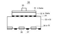
- FIG. 7 is a schematic cross-sectional view of a GaAs // Si multi-junction solar cell 30 having an alternate back electrode structure.
- a GaAs solar cell having the n-type GaAs layer 31 formed on the light incident side of the p-type GaAs layer 32 is used as the top cell.
- the top cell includes a top electrode 35 on the light incident side.
- n-type and p-type electrodes n-type back electrode 37 and p-type back electrode 36
- a region of the p-type Si portion 38 is formed in a partial region of the n-type Si layer 33 on the back surface side of the substrate, and a p-type back electrode 36 connected to the p-type Si 38 is formed.
- the conventional solar spectrum in the GaAs top cell and Si bottom cell, respectively, current of about 30 mA / cm 2 and 10 mA / cm 2 is produced.
- the size (surface area) of the subcell is adjusted so that the photoelectric flow generated in the top cell and the bottom cell becomes uniform and the current matching condition is satisfied.
- surplus photocurrent generated in the bottom cell due to the spectrum fluctuation of sunlight is taken out as electric power from the backside alternating electrodes.
- FIG. 8 is a schematic sectional view of a GaAs // Si multi-junction solar cell 40 having an intermediate electrode structure.
- a GaAs solar cell in which the n-type GaAs layer 41 is formed on the light incident side of the p-type GaAs layer 42 is used.
- the top cell includes a top electrode 45 on the light incident side.
- an Si solar cell having an n-type Si layer 48 and an intermediate electrode 47 formed on the light incident side of the substrate of the p-type Si layer 49 is used.
- a p-type back electrode 46 is provided on the back side of the bottom cell.
- the bonding layer 44 made of conductive nanoparticles By bonding the top cell and the bottom cell using the bonding layer 44 made of conductive nanoparticles, a three-terminal multi-junction solar cell is formed. Pd nanoparticles are used as the conductive nanoparticles.
- the size (surface area) of the subcell is adjusted so that the photoelectric flow generated in the top cell and the bottom cell becomes uniform and the current matching condition is satisfied.
- the excess photocurrent generated in the GaAs top cell due to the spectrum fluctuation of sunlight is taken out as electric power using the intermediate electrode and the top electrode. Excess photocurrent generated in the bottom cell is extracted as power using the back electrode and the intermediate electrode.
- FIG. 9 is a schematic cross-sectional view of a GaAs / GaAs // Si multi-junction solar cell 50 having an alternate back electrode structure.
- a GaAs subcell consisting of an n-type GaAs layer 51 and a p-type GaAs layer 52
- a tunnel junction layer 53 is used as a top cell.
- a GaAs subcell consisting of an n-type GaAs layer 58 and a p-type GaAs layer 59
- the top cell includes a top electrode 55 on the light incident side.
- a Si solar cell in which n-type and p-type electrodes (n-type back electrode 57 and p-type back electrode 56) are alternately formed on the back surface side of the substrate of the n-type Si layer 61 is used.
- a p-type Si 62 region is formed in a partial region of the n-type Si layer 61 on the back surface side of the substrate, and a p-type back electrode 56 connected to the p-type Si 62 is formed.
- a three-terminal multi-junction (three-junction) solar cell is formed.
- Pd nanoparticles are used as the conductive nanoparticles.
- a current of about 10 mA / cm 2 is generated.
- the size (surface area) of the subcell is adjusted so that the photoelectric flow generated in the top cell and the bottom cell becomes uniform and the current matching condition is satisfied.
- surplus photocurrent generated in the bottom cell due to the spectrum fluctuation of sunlight is taken out as electric power from the backside alternating electrodes.
- FIG. 10 is a schematic cross-sectional view of a GaInP / GaAs // GaInAsP / GaInAs multi-junction solar cell 70 having an intermediate electrode structure.
- a GaInP subcell (consisting of an n-type GaInP layer 71 and a p-type GaInP layer 72), a tunnel junction layer 73 and a GaAs subcell (consisting of an n-type GaAs layer 78 and a p-type GaAs layer 79) are used.
- GaInP / GaAs2 junction solar cell is used.
- the top cell includes a top electrode 75 on the light incident side.
- the bottom cell includes a GaInAsP subcell (consisting of an n-type GaInAsP layer 80 and a p-type GaInAsP layer 81), a tunnel junction layer 82, and a GaInAs subcell (consisting of an n-type GaInAs layer 83 and a p-type GaInAs layer 84).
- a GaInAsP / GaInAs2 junction solar cell is used.
- a solar cell in which an intermediate electrode 77 is formed on a part other than the junction surface on the n-type GaInAsP layer 80 located on the light incident side of the p-type GaInAsP layer 81 is used.
- a p-type back electrode 76 is provided on the back side of the bottom cell.
- a three-terminal multi-junction (four-junction) solar cell is formed by bonding the top cell and the bottom cell using the bonding layer 74 made of conductive nanoparticles.
- the size (surface area) of the subcell is adjusted so that the photoelectric flow generated in the top cell and the bottom cell becomes uniform and the current matching condition is satisfied.
- an excess photocurrent generated in the GaInP / GaAs top cell due to the fluctuation of the spectrum of sunlight is taken out as power using the intermediate electrode and the top electrode.
- Excess photocurrent generated in the GaInAsP / GaInAs bottom cell is extracted as power using the back electrode and the intermediate electrode.
- the multi-junction photoelectric conversion element of the present invention has been described by using examples of a plurality of types of solar cells.
- the cells of the photoelectric conversion element used in the present invention are not limited to those illustrated.
- the photoelectric conversion element or solar cell of the present invention is industrially useful because it is a device that improves the use efficiency of light energy such as sunlight and is robust against fluctuations in the spectrum of sunlight.
- Second basic structure 26 Second electrode 30 GaAs // Si multi-junction solar cell with alternate back electrode structure 31, 41, 51, 58, 78 n-type GaAs layer 32, 42, 52, 59, 79 p-type GaAs layers 33, 48, 61 n-type Si layers 36, 46, 56, 76 p-type back electrode 37, 57 n-type back electrode 38, 62 p-type Si Reference Signs List 40
Abstract
Provided are: a multijunction photoelectric conversion element which has robustness against spectrum fluctuations, which is provided with high-quality crystal sub-cells, and in which optical reflection loss in a bonded portion is reduced; a multijunction solar battery; and a manufacturing method for the multijunction photoelectric conversion element. The multijunction photoelectric conversion element is provided with: a first cell (12) which is a photoelectric conversion element positioned on the light incident side; a second cell (13) which is a photoelectric conversion element positioned on a side opposite to the light incident side; a junction layer (14) with which the first cell (12) and the second cell (13) are bonded together, and which is made from conductive nanoparticles; a first electrode (15) positioned on the light incident-side surface of the first cell (12); a second electrode (16) positioned on a surface, of the second cell (13), opposite to the light incident side; and a third electrode which is provided to the second cell (13), and which is an electrode (17) positioned on the surface opposite to the light incident side or is an intermediate electrode positioned on the first cell (12)-side surface. Accordingly, a high-performance multijunction photoelectric conversion element can be implemented.
Description
本発明は、複数の光電変換素子のセルを接合してなる多接合光電変換素子及び該多接合光電変換素子を備える多接合太陽電池、並びに多接合光電変換素子の製造方法に関する。
The present invention relates to a multi-junction photoelectric conversion element formed by joining cells of a plurality of photoelectric conversion elements, a multi-junction solar cell including the multi-junction photoelectric conversion element, and a method for manufacturing a multi-junction photoelectric conversion element.
近年、多接合太陽電池に代表される多接合の光電変換素子の研究開発が進められている。多接合太陽電池は、バンドギャップエネルギーの異なる半導体素子からなる太陽電池セルを複数積層した構造を有する。多接合太陽電池では、異なる波長の太陽光を吸収する太陽電池セルを直列につなぎ合わせることにより、広くエネルギー分布した太陽光を効率よく利用できる。多接合太陽電池の出力電圧は、各セルの電圧の合計になるので大きくなる。
In recent years, research and development of multi-junction photoelectric conversion elements represented by multi-junction solar cells have been promoted. A multi-junction solar cell has a structure in which a plurality of solar cells composed of semiconductor elements having different band gap energies are stacked. In a multi-junction solar cell, solar cells that absorb sunlight of different wavelengths are connected in series, so that sunlight with a wide energy distribution can be used efficiently. The output voltage of the multi-junction solar cell increases because it is the sum of the voltages of the cells.
多接合の光電変換素子や多接合太陽電池を構成するところの、個々の光電変換素子や太陽電池の各セルを、サブセルともいう。多接合太陽電池の光入射側(最表面側)に置かれている太陽電池をトップセルという。トップセルには、バンドギャップが大きい半導体を用い、それより短波長の光を吸収して長波長の光を透過させる。一方、光入射側に対して最も反対側に置かれるのがボトムセルである。ボトムセルには、バンドギャップが小さい半導体を使用し、トップセルを透過した光を吸収する。3接合太陽電池の場合、真ん中の太陽電池をミドルセルと言う。
セ ル Each photoelectric conversion element or each cell of a solar cell constituting a multi-junction photoelectric conversion element or a multi-junction solar cell is also referred to as a subcell. A solar cell placed on the light incident side (outermost surface side) of the multi-junction solar cell is called a top cell. For the top cell, a semiconductor having a large band gap is used, and light having a shorter wavelength is absorbed and light having a longer wavelength is transmitted. On the other hand, the bottom cell is located farthest from the light incident side. A semiconductor having a small band gap is used for the bottom cell, and absorbs light transmitted through the top cell. In the case of a three-junction solar cell, the middle solar cell is called a middle cell.
図11は、従来の2端子型の多接合太陽電池の模式的構造断面図である。図11のように、2端子型の多接合太陽電池は、トップセル2とボトムセル3が積層された積層構造であり、光入射側から見て表面と裏面に、電気エネルギーを取り出すための電極(トップ電極5と裏面電極6)を備える2端子構造を有する。
FIG. 11 is a schematic cross-sectional view of a conventional two-terminal multi-junction solar cell. As shown in FIG. 11, the two-terminal type multi-junction solar cell has a stacked structure in which a top cell 2 and a bottom cell 3 are stacked, and electrodes (for extracting electric energy) are provided on the front surface and the back surface when viewed from the light incident side. It has a two-terminal structure including a top electrode 5 and a back electrode 6).
図12に、図11の2端子型の多接合太陽電池の等価回路図を示す。2端子型の多接合太陽電池において、直列に接続された各サブセルには同一の電流が流れる。図12の電流I1と電流I2と電流I3が等しい。この電流整合条件のために、各サブセルにおいては、光吸収により生成された光電流量が最も低い値であるサブセルの光電流量によって、2端子型多接合太陽電池を流れる電流量が決定される。高い光電流量が生成されたサブセルにおいては、逆電流(暗電流)が生成し、流れる電流量が生成された光電流値よりも低減してしまう。また、地上で利用する際には太陽光スペクトルの変動などにより、各サブセルにおいて生成される光電流量は変動するため、電流整合条件を満たす必要のある2端子型多接合太陽電池は、太陽光スペクトル変動による損失が生じやすい。
FIG. 12 shows an equivalent circuit diagram of the two-terminal multi-junction solar cell of FIG. In a two-terminal multi-junction solar cell, the same current flows through each sub-cell connected in series. Equal currents I 1 and the current I 2 and the current I 3 in FIG. Due to this current matching condition, in each subcell, the amount of current flowing through the two-terminal multi-junction solar cell is determined by the photoelectric flow of the subcell in which the photoelectric flow generated by light absorption is the lowest value. In a subcell in which a high photoelectric flow rate is generated, a reverse current (dark current) is generated, and the amount of flowing current is smaller than the generated photocurrent value. In addition, when used on the ground, the photoelectric flow generated in each sub-cell varies due to fluctuations in the solar spectrum and the like. Losses due to fluctuations are likely to occur.
スペクトル変動による損失を低減する方法として、電極をサブセル間に配置する4端子型等の多電極端子型の多接合デバイス構造が提案されている(非特許文献1参照)。
As a method of reducing loss due to spectrum fluctuation, a multi-electrode terminal type multi-junction device structure such as a four-terminal type in which electrodes are arranged between subcells has been proposed (see Non-Patent Document 1).
図13は、4端子型の多接合太陽電池の等価回路図である。4端子型の多接合太陽電池は、トップセル2とボトムセル3を電気的に分離した回路で構成される。各サブセルで生成された光電流(電流I2(電流I1)、電流I4(電流I3))が、それぞれ出力電力(電圧V1、電圧V2)として出力される。電流律速条件が課されていないため、太陽光スペクトル変動による損失が生じにくい。
FIG. 13 is an equivalent circuit diagram of a four-terminal multi-junction solar cell. The four-terminal multi-junction solar cell is configured by a circuit in which the top cell 2 and the bottom cell 3 are electrically separated. Photocurrent generated by each subcell (current I 2 (current I 1), the current I 4 (current I 3)) is output as the respective output power (voltage V 1, the voltage V 2). Since no current limiting condition is imposed, loss due to fluctuations in the solar spectrum is unlikely to occur.
図14は、4端子型の多接合太陽電池の模式的構造断面図である。図14のように、4端子型の多接合太陽電池は、トップセル2とボトムセル3が積層された構造であり、トップセル2とボトムセル3の電力をそれぞれ出力するために、4端子を有する。4端子は、光入射側から順に、トップセル2の表面のトップ電極5と、トップセル裏面に積層される透明電極層8aに電気接続される中間電極7aと、ボトムセル3の表面に積層される透明電極層8bに設けられる中間電極7bと、ボトムセル裏面の裏面電極6とである。トップセル2の裏面の透明電極層8aと、ボトムセル3の表面の透明電極層8bの間には、透明電極層を互いに電気的に絶縁するための絶縁接着層9が配置される。透明電極層及び絶縁接着層には、光吸収損失を低減するために透明な材料が用いられる。
FIG. 14 is a schematic cross-sectional view of a four-terminal multi-junction solar cell. As shown in FIG. 14, the four-terminal multi-junction solar cell has a structure in which a top cell 2 and a bottom cell 3 are stacked, and has four terminals to output power of the top cell 2 and the bottom cell 3 respectively. The four terminals are sequentially stacked from the light incident side on the top electrode 5 on the surface of the top cell 2, the intermediate electrode 7a electrically connected to the transparent electrode layer 8a stacked on the back surface of the top cell, and the surface of the bottom cell 3. The intermediate electrode 7b provided on the transparent electrode layer 8b and the back electrode 6 on the back surface of the bottom cell. Between the transparent electrode layer 8a on the back surface of the top cell 2 and the transparent electrode layer 8b on the surface of the bottom cell 3, an insulating adhesive layer 9 for electrically insulating the transparent electrode layers from each other is arranged. For the transparent electrode layer and the insulating adhesive layer, a transparent material is used to reduce light absorption loss.
図15は、3端子型の多接合太陽電池の等価回路図である。3端子型の多接合太陽電池は、トップセル2とボトムセル3の間に中間電極を配置した回路で構成される。図15のように、トップセルに流れる電流をI2、ボトムセルに流れる電流をI3、各端子に流れる電流を(電流I1、電流I4、電流I5)、多接合デバイスの電圧をV1、ボトムセルの電圧をV2で表す。トップセルまたはボトムセルで生じた余剰の光電流は、中間電極を介して電力として出力される。これにより、トップセルとボトムセルは電流整合条件を満たす必要がなくなり、スペクトル変動等によりトップセルとボトムセルで生成される光電流量が不均等になった場合にも、余剰の暗電流を生成せずに済む。
FIG. 15 is an equivalent circuit diagram of a three-terminal multi-junction solar cell. The three-terminal multi-junction solar cell is constituted by a circuit in which an intermediate electrode is arranged between a top cell 2 and a bottom cell 3. As shown in FIG. 15, the current flowing to the top cell is I 2 , the current flowing to the bottom cell is I 3 , the current flowing to each terminal is (current I 1 , current I 4 , current I 5 ), and the voltage of the multi-junction device is V 1 represents the voltage of the bottom cell in V 2. Excess photocurrent generated in the top cell or the bottom cell is output as electric power via the intermediate electrode. As a result, the top cell and the bottom cell do not need to satisfy the current matching condition, and even when the photoelectric flow generated in the top cell and the bottom cell becomes uneven due to spectrum fluctuation or the like, an excess dark current is not generated. I'm done.
図16は、従来の3端子型の多接合太陽電池の構造図である。3端子は、光入射側から順に、トップセル2の表面のトップ電極5と、中間電極7と、ボトムセル裏面の裏面電極6とである。図16のように、3端子型の多接合太陽電池は、トップセル2とボトムセル3を連続して成長させて積層構造を作製し、該積層構造の中間に中間電極7を後から取り付ける方法で作製されてきた。例えば、Si系のボトムセル上にGaAs系のトップセルを直接結晶成長させる方法により、多接合型太陽電池を作製する方法が知られている(非特許文献2参照)。
FIG. 16 is a structural view of a conventional three-terminal multi-junction solar cell. The three terminals are, in order from the light incident side, a top electrode 5 on the front surface of the top cell 2, an intermediate electrode 7, and a back electrode 6 on the back surface of the bottom cell. As shown in FIG. 16, the three-terminal type multi-junction solar cell has a method in which a top cell 2 and a bottom cell 3 are continuously grown to form a laminated structure, and an intermediate electrode 7 is attached later in the middle of the laminated structure. It has been made. For example, a method of manufacturing a multi-junction solar cell by a method of directly growing a GaAs-based top cell on a Si-based bottom cell is known (see Non-Patent Document 2).
図17は、非特許文献3に示された3端子型太陽電池である。トップセル2にトップ電極5を設け、ボトムセル3裏面に交互電極6a、6bを形成した3端子型太陽電池が提案されている。しかし、トランジスタ構造と類似の構造(np/p-(p,n))となっており、多接合太陽電池(np/np)とは回路構成が異なっている。
FIG. 17 shows a three-terminal solar cell disclosed in Non-Patent Document 3. A three-terminal solar cell in which a top electrode 5 is provided on a top cell 2 and alternate electrodes 6a and 6b are formed on the back surface of the bottom cell 3 has been proposed. However, it has a structure similar to the transistor structure (np / p- (p, n)), and has a different circuit configuration from the multi-junction solar cell (np / np).
本発明者らは、先に、導電性ナノ粒子を用いた接合によりトップセルとボトムセルを貼り合わせることにより、異種半導体材料のサブセルからなる多接合太陽電池を、提案した(特許文献1、非特許文献4、非特許文献5参照)。
The present inventors have previously proposed a multi-junction solar cell composed of sub-cells of heterogeneous semiconductor materials by bonding a top cell and a bottom cell by bonding using conductive nanoparticles (Patent Document 1, Non-Patent Document 1). Reference 4, Non-patent Reference 5).
従来技術の2端子構造の多接合光電変換素子は、高い光電流量が生成されたサブセルにおいて、逆電流(暗電流)が生成し、流れる電流量が生成された光電流値よりも低減してしまうという問題がある。また、電流整合条件を満たす必要のある2端子型多接合太陽電池は、太陽光スペクトルの変動などにより、各サブセルにおいて生成される光電流量が変動するため、太陽光スペクトル変動による損失が生じやすいという問題がある。
In a conventional multi-junction photoelectric conversion device having a two-terminal structure, a reverse current (dark current) is generated in a subcell in which a high photoelectric flow is generated, and the amount of flowing current is smaller than the generated photocurrent value. There is a problem. In addition, in a two-terminal multi-junction solar cell that needs to satisfy the current matching condition, the photoelectric flow generated in each subcell fluctuates due to fluctuations in the solar spectrum or the like. There's a problem.
従来技術の4端子型の多接合デバイスにおいては、トップセルとボトムセルの接合部に、透明電極層及び絶縁接着層を設ける必要があった。このように、接合部には、光吸収損失を低減するために透明な材料を用いる必要があった。しかし、接合部の全材料を透明にしても、トップセルとボトムセルの間に挿入される透明電極・透明な接着剤による光学反射損失やトップセルの結晶品質が低下してしまう問題がある。また、半導体/透明電極層および透明電極層/絶縁接着層における屈折率の違いに起因した光学反射が生じてしまい、損失要因となってしまうという問題がある。
(4) In the conventional four-terminal multi-junction device, it is necessary to provide a transparent electrode layer and an insulating adhesive layer at the junction between the top cell and the bottom cell. Thus, it was necessary to use a transparent material for the joint in order to reduce light absorption loss. However, even if the entire material of the bonding portion is transparent, there is a problem that optical reflection loss due to a transparent electrode and a transparent adhesive inserted between the top cell and the bottom cell and the crystal quality of the top cell are degraded. Further, there is a problem that optical reflection occurs due to a difference in the refractive index between the semiconductor / transparent electrode layer and the transparent electrode layer / insulating adhesive layer, which causes a loss.
従来技術の3端子型の多接合デバイスの例のように、Siボトムセル上にGaAsトップセルを直接結晶成長する製造方法では、GaAs結晶の品質が低下してしまい、良好な太陽電池特性が得られないという問題がある。
In a manufacturing method in which a GaAs top cell is directly crystal-grown on a Si bottom cell as in an example of a conventional three-terminal type multi-junction device, the quality of the GaAs crystal deteriorates, and good solar cell characteristics can be obtained. There is no problem.
非特許文献3に示された従来技術は、多接合太陽電池(np/np)とは回路構成が異なっている。即ち、非特許文献3は、次の問題を解決するために裏面交互電極が設けられたものである。通常の入射光側の電極は入射光を遮りセルに影を生じてしまうため、電流生成の損失要因となっていた。この電極による光反射・散乱損失を解消する方法として、裏面交互型電極が導入された。これによって、入射面側での電極による光損失が低減され、高い電流生成が実現している。非特許文献3は、pn接合の直列接続になっていないので、タンデム(2つが縦に並んでいる構造)ではあるが、本願が目的とする多接合太陽電池のようにpn接合を直列に接合することによって高い電圧が得られるような構造になっていない。
従 来 The prior art shown in Non-Patent Document 3 has a different circuit configuration from a multi-junction solar cell (np / np). That is, Non-Patent Literature 3 discloses that a back surface alternate electrode is provided to solve the following problem. The normal electrode on the incident light side blocks the incident light and creates a shadow on the cell, which has been a factor of loss of current generation. As a method of eliminating the light reflection / scattering loss due to this electrode, an alternate back type electrode has been introduced. Thereby, light loss due to the electrode on the incident surface side is reduced, and high current generation is realized. Non-Patent Document 3 is a tandem (a structure in which two are arranged vertically) because a pn junction is not connected in series. The structure does not provide a high voltage.
また、従来技術の導電性ナノ粒子による接合を用いる提案は、2端子構造に関する技術であり、多接合太陽電池における電流律速による制限を解決できていなかった。
提案 Also, the prior art proposal using bonding with conductive nanoparticles is a technology relating to a two-terminal structure, and has not been able to solve the limitation due to current limiting in a multi-junction solar cell.
本発明は、これらの問題を解決しようとするものであり、スペクトル変動に対して堅牢で、高品質結晶の各サブセルを備え、接合部における光学反射損失の低減した、多接合光電変換素子を提供することを目的とする。前記多接合光電変換素子の製造方法を提供することを目的とする。また、前記多接合光電変換素子を備える多接合太陽電池を提供することを目的とする。
The present invention seeks to solve these problems, and provides a multi-junction photoelectric conversion element that is robust against spectral fluctuations, has subcells of high-quality crystals, and has a reduced optical reflection loss at the junction. The purpose is to do. An object of the present invention is to provide a method for manufacturing the multi-junction photoelectric conversion element. Moreover, it aims at providing the multi-junction solar cell provided with the said multi-junction photoelectric conversion element.
本発明は、前記目的を達成するために、以下の特徴を有するものである。
The present invention has the following features to achieve the above object.
(1) 多接合光電変換素子であって、光入射側に位置する光電変換素子の第1のセルと、光入射側の反対側に位置する光電変換素子の第2のセルと、前記第1のセルと前記第2のセルを接合する、導電性ナノ粒子からなる接合層と、前記第1のセルの、光入射側の面に位置する第1の電極と、前記第2のセルの、光入射側の反対面に位置する第2の電極と、前記第2のセルに設けた第3の電極であって、光入射側の反対面に位置する電極、または、第1のセル側の面に位置する中間電極である前記第3の電極と、を備えることを特徴とする多接合光電変換素子。
(2) 前記第3の電極を利用して、前記第1のセル又は前記第2のセルに生じた余剰の光電流を電力として取り出すことを特徴とする前記(1)記載の多接合光電変換素子。
(3) 前記第2のセルの表面積は、前記第1のセルの表面積より大であることを特徴とする前記(1)又は(2)記載の多接合光電変換素子。
(4) 前記導電性ナノ粒子の表面は有機分子で覆われていないことを特徴とする前記(1)乃至(3)のいずれか1項に記載の多接合光電変換素子。
(5) 前記接合層は、前記導電性ナノ粒子からなる接合層の厚みが、5ナノメートル以上50ナノメートル以下であることを特徴とする前記(1)乃至(4)のいずれか1項に記載の多接合光電変換素子。
(6) 前記多接合光電変換素子の前記セルが、結晶Si系、アモルファスSi系、微結晶Si系、有機系、もしくは、カルコパイライト系材料を用いた単接合太陽電池、またはGaAs、InP、GaSb、もしくは、Ge基板上等に積層された2接合以上からなる太陽電池であることを特徴とする前記(1)乃至(5)のいずれか1項に記載の多接合光電変換素子。
(7) 前記(1)乃至(6)のいずれか1項に記載の多接合光電変換素子を備える多接合型太陽電池。
(8) 光入射側に位置する光電変換素子の第1のセルと、光入射側の反対側に位置する光電変換素子の第2のセルと、を備える多接合光電変換素子の製造方法であって、前記第2のセルに、光入射側の反対面に位置する第2の電極を形成すると共に、光入射側の反対面に位置する第3の電極、または、第1のセル側の面に位置する中間電極となる第3の電極を設ける工程と、前記第1のセルを前記第2のセルに、有機分子で覆われていない導電性ナノ粒子により接合する接合工程と、前記第1のセルの、光入射側の面に第1の電極を形成する工程と、を備えることを特徴とする多接合光電変換素子の製造方法。 (1) a multi-junction photoelectric conversion element, wherein a first cell of the photoelectric conversion element located on the light incident side, a second cell of the photoelectric conversion element located on the side opposite to the light incident side, A bonding layer made of conductive nanoparticles for bonding the cell and the second cell, a first electrode located on a light incident side surface of the first cell, and a A second electrode located on the surface opposite to the light incident side, and a third electrode provided on the second cell, the electrode being located on the surface opposite to the light incident side, or a third electrode provided on the first cell side. And a third electrode, which is an intermediate electrode located on the surface.
(2) The multi-junction photoelectric conversion according to (1), wherein an excess photocurrent generated in the first cell or the second cell is taken out as electric power using the third electrode. element.
(3) The multi-junction photoelectric conversion element according to (1) or (2), wherein the surface area of the second cell is larger than the surface area of the first cell.
(4) The multi-junction photoelectric conversion element according to any one of (1) to (3), wherein a surface of the conductive nanoparticle is not covered with an organic molecule.
(5) The bonding layer according to any one of (1) to (4), wherein a thickness of the bonding layer including the conductive nanoparticles is 5 nm or more and 50 nm or less. The multi-junction photoelectric conversion element according to the above.
(6) The cell of the multi-junction photoelectric conversion element is a single-junction solar cell using crystalline Si, amorphous Si, microcrystalline Si, organic, or chalcopyrite-based material, or GaAs, InP, GaSb. Alternatively, the multi-junction photoelectric conversion element according to any one of the above (1) to (5), which is a solar cell including two or more junctions stacked on a Ge substrate or the like.
(7) A multi-junction solar cell comprising the multi-junction photoelectric conversion element according to any one of (1) to (6).
(8) A method for manufacturing a multi-junction photoelectric conversion element, comprising: a first cell of a photoelectric conversion element located on a light incident side; and a second cell of a photoelectric conversion element located on a side opposite to the light incident side. Forming a second electrode on the second cell opposite to the light incident side, and forming a third electrode opposite the light incident side on the second cell, or a surface on the first cell side. Providing a third electrode serving as an intermediate electrode located in the first cell, bonding the first cell to the second cell with conductive nanoparticles not covered with organic molecules, Forming a first electrode on the light-incident side surface of the cell described in (1).
本発明の多接合光電変換素子は、異種材料からなるサブセルを用い、導電性ナノ粒子からなる接合層により接合し、かつ3端子を設けることにより、広くエネルギー分布した太陽光等を高効率で利用可能とし、かつ多接合太陽電池を構成する各サブセルに生じる光電流値の不均衡による損失を抑制するという効果を奏する。よって、本発明の多接合光電変換素子は、スペクトル変動に対して堅牢である。また、本発明の多接合光電変換素子は、導電性ナノ粒子による接合層により各サブセルが接合されるので、各サブセルを高品質結晶で構成することが可能であり、各サブセルが高性能である。また、本発明の多接合光電変換素子は、接合層が導電性ナノ粒子からなる接合層であることにより、接合部における光学反射損失の低減した多接合光電変換素子を実現できる。
The multi-junction photoelectric conversion element of the present invention uses sub-cells made of different materials, is bonded by a bonding layer made of conductive nanoparticles, and is provided with three terminals, so that sunlight with a wide energy distribution can be used with high efficiency. It is possible to achieve the effect of suppressing the loss due to the imbalance of the photocurrent value generated in each subcell constituting the multi-junction solar cell. Therefore, the multi-junction photoelectric conversion element of the present invention is robust against spectrum fluctuation. Further, in the multi-junction photoelectric conversion element of the present invention, since each sub-cell is joined by a joining layer made of conductive nanoparticles, each sub-cell can be made of a high-quality crystal, and each sub-cell has high performance. . Moreover, the multi-junction photoelectric conversion element of the present invention can realize a multi-junction photoelectric conversion element with reduced optical reflection loss at the junction because the junction layer is a junction layer made of conductive nanoparticles.
本発明の多接合太陽電池は、前記本発明の多接合光電変換素子から構成されるので、広くエネルギー分布した太陽光等を高効率で利用可能とし、かつスペクトル変動に対して堅牢である。
多 Since the multi-junction solar cell of the present invention is constituted by the multi-junction photoelectric conversion element of the present invention, it is possible to efficiently use sunlight or the like having a wide energy distribution and is robust against spectrum fluctuation.
本発明の多接合光電変換素子の製造方法では、予め形成した第2及び第3の電極付きの光電変換素子をボトムセルに用い、これとトップセルを貼り合わせることによって、高結晶品質のセルをそれぞれ使用できるので、従来の3端子型デバイスと比較して、高性能の多接合光電変換素子を製造できる。
In the method for manufacturing a multi-junction photoelectric conversion element of the present invention, a pre-formed photoelectric conversion element with second and third electrodes is used for a bottom cell, and this and a top cell are bonded to each other to obtain a high-crystal quality cell. Since it can be used, a high-performance multi-junction photoelectric conversion element can be manufactured as compared with a conventional three-terminal device.
本発明の実施形態について以下説明する。
(4) An embodiment of the present invention will be described below.
本発明者らは、複数の光電変換素子のセルが接合された光電変換素子において、接合構造と端子構造の開発により、太陽光エネルギー等の高効率化、及び太陽光のスペクトル変動による損失の軽減を実現したものである。
The present inventors have developed a junction structure and a terminal structure in a photoelectric conversion element in which a plurality of cells of a photoelectric conversion element are joined, thereby increasing the efficiency of solar energy and the like, and reducing the loss due to spectrum fluctuation of sunlight. Is realized.
本発明の実施形態の多接合光電変換素子は、複数の光電変換素子のセルが接合されてなる光電変換素子に関し、光入射側に位置する光電変換素子の第1のセル(以下、「トップセル」ともいう。)と、光入射側の反対側に位置する光電変換素子の第2のセル(以下、「ボトムセル」ともいう。)と、前記第1のセルと前記第2のセルを接合する、有機分子で覆われていない導電性ナノ粒子からなる接合層と、を含む積層構造を有する。
A multi-junction photoelectric conversion element according to an embodiment of the present invention relates to a photoelectric conversion element in which cells of a plurality of photoelectric conversion elements are joined, and relates to a first cell (hereinafter, referred to as a “top cell”) of a photoelectric conversion element located on a light incident side. ), And the second cell (hereinafter, also referred to as a “bottom cell”) of the photoelectric conversion element located on the side opposite to the light incident side, and the first cell and the second cell are joined. And a bonding layer made of conductive nanoparticles that are not covered with organic molecules.
本発明の実施形態の多接合光電変換素子は、3つの電極からの端子を有するので、3端子型の多接合光電変換素子である。3端子は、前記第1のセルの、光入射側の面に位置する第1の電極の端子と、前記第2のセルの、光入射側の反対面に位置する第2の電極の端子と、前記第2のセルに設けた第3の電極の端子である。第3の電極は、光入射側の反対面に位置する電極、または、第1のセル側の面に位置する中間電極のいずれか1つである。
多 Since the multi-junction photoelectric conversion element according to the embodiment of the present invention has terminals from three electrodes, it is a three-terminal multi-junction photoelectric conversion element. The three terminals include a first electrode terminal located on a light incident side surface of the first cell and a second electrode terminal located on a light incident side opposite surface of the second cell. , Terminals of a third electrode provided in the second cell. The third electrode is one of an electrode located on a surface opposite to the light incident side and an intermediate electrode located on a surface on the first cell side.
第3の電極を光入射側の反対面に位置する電極で構成した、3端子型の多接合光電変換素子(以下、「第1の基本構造」という。)について、図1乃至3を参照して説明する。図1は、3端子型多接合光電変換素子の第1の基本構造10の模式的構造断面図である。図2は、第1の基本構造の斜視図である。図3は、第1の基本構造のボトムセルの裏面の交互電極16、17を説明する図である。裏面の交互電極の一方がn型で、他方がp型である。第1の基本構造は、トップセル12とボトムセル13とこれらを接合する導電性ナノ粒子からなる接合層14からなる積層構造を備え、トップセルの光入射側面にトップ電極15を備え、ボトムセル13の裏面に、従来の第2の電極の他に、さらに、第3の電極を設けた電極構造を有する。ボトムセル13の裏面における電極構造は、第2の電極と第3の電極とが交互に配置された交互電極構造を有する。細い線状の電極が並列に配置された電極部分を、グリッドとも呼ぶ。交互電極構造を構成する第2の電極と第3の電極は、それぞれ交互電極部分より太い線(バスバー電極)等で接続されて、第2の電極、第3の電極を構成する。例えば、第2の電極と、第3の電極を、それぞれ櫛形とし、それぞれの櫛形の櫛歯が交互に入り込む構造とすることができる。なお、櫛形に限定されない。
A three-terminal multi-junction photoelectric conversion element (hereinafter, referred to as a “first basic structure”) in which a third electrode is formed of an electrode located on a surface opposite to a light incident side will be described with reference to FIGS. Will be explained. FIG. 1 is a schematic structural sectional view of a first basic structure 10 of a three-terminal multi-junction photoelectric conversion element. FIG. 2 is a perspective view of the first basic structure. FIG. 3 is a diagram illustrating the alternating electrodes 16 and 17 on the back surface of the bottom cell having the first basic structure. One of the alternate electrodes on the back is n-type and the other is p-type. The first basic structure has a stacked structure including a top cell 12, a bottom cell 13, and a bonding layer 14 made of conductive nanoparticles for bonding them, a top electrode 15 is provided on a light incident side surface of the top cell, and a bottom cell 13 is formed. On the back surface, there is an electrode structure in which a third electrode is provided in addition to the conventional second electrode. The electrode structure on the back surface of the bottom cell 13 has an alternate electrode structure in which second electrodes and third electrodes are alternately arranged. The electrode portion where thin linear electrodes are arranged in parallel is also called a grid. The second electrode and the third electrode constituting the alternating electrode structure are connected to each other with a thicker line (bus bar electrode) or the like than the alternating electrode portion, thereby forming a second electrode and a third electrode. For example, the second electrode and the third electrode may have a comb shape, and the comb teeth of each comb may alternately enter. In addition, it is not limited to a comb shape.
第1の基本構造は、前記3端子型の多接合太陽電池のpn接合の位置が裏面側に移動しているが、等価回路図としては図15と同じである。トップ電極15と電極17の間にはトップセル12とボトムセル13で生成された電圧を足し合わせた電圧が生じる。例えば、トップセル12で生成された電流I2がボトムセル13で生成された電流I3よりも小さい場合には、トップ電極15と電極17の間を流れる電流はトップセル12で生成された電流I2で律速されるため、電流I2が流れる。また、電極16と電極17の間には、ボトムセル13で生成された電圧が生じる。ボトムセル13で生じた電流I3のうちトップ電極15と電極17の間に流れる電流を差し引いた電流I5(=I3-I2)が流れる。第1の電極(トップ電極)と第2の電極(裏面交互電極の一方)とにより、第1のセル(トップセル)に生じた余剰の光電流を電力として取り出し、第2の電極(裏面交互電極の一方)と第3の電極(裏面交互電極の他方)とにより、第2のセル(ボトムセル)に生じた余剰の光電流を電力として取り出す。
In the first basic structure, the position of the pn junction of the three-terminal type multi-junction solar cell is moved to the back side, but the equivalent circuit diagram is the same as that in FIG. A voltage is generated between the top electrode 15 and the electrode 17 by adding the voltages generated by the top cell 12 and the bottom cell 13. For example, when the current I 2 generated in the top cell 12 is smaller than the current I 3 generated in the bottom cell 13, the current flowing between the top electrode 15 and the electrode 17 becomes the current I 2 generated in the top cell 12. to be rate-limiting in 2, current I 2 flows. Further, a voltage generated in the bottom cell 13 is generated between the electrode 16 and the electrode 17. A current I 5 (= I 3 −I 2 ) obtained by subtracting a current flowing between the top electrode 15 and the electrode 17 from the current I 3 generated in the bottom cell 13 flows. An excess photocurrent generated in the first cell (top cell) is taken out as electric power by the first electrode (top electrode) and the second electrode (one of the backside alternating electrodes), and the second electrode (backside alternating electrode) is taken out. The excess photocurrent generated in the second cell (bottom cell) is extracted as power by one of the electrodes) and the third electrode (the other of the backside alternating electrodes).
第3の電極を、第1のセル側の面に位置する中間電極で構成した、多接合光電変換素子(以下、「第2の基本構造」という。)について、図4乃至6を参照して説明する。図4は、3端子型多接合光電変換素子の第2の基本構造20の模式的構造断面図である。図5は、第2の基本構造の斜視図である。図6は、第2の基本構造の、中間電極を形成したボトムセルの上面図である。第2の基本構造は、トップセル22とボトムセル23とこれらを接合する導電性ナノ粒子からなる接合層24とからなる積層構造を備え、トップセルの光入射側にトップ電極25を設け、ボトムセル23の裏面に第2の電極26を設け、さらに、ボトムセル23の上面(トップセル側の面)に中間電極27となる第3の電極を設けた電極構造を有する。中間電極27は、ボトムセル23の上面であれば、トップセル22との接合部以外の位置であればどこでもよい。図6(a)(b)は、細い電極線が並列に配置されたグリッドと、該グリッドを接続するより太い電極(バスバー電極)とからなる中間電極である。(a)は櫛形の例であり、(b)はバスバー電極を複数設ける例である。なお、中間電極の形状は特に限定されない。グリッドを細い電線で構成して遮光しないことが好ましい。
Regarding a multi-junction photoelectric conversion element (hereinafter, referred to as “second basic structure”) in which a third electrode is constituted by an intermediate electrode located on the surface on the first cell side, with reference to FIGS. explain. FIG. 4 is a schematic structural cross-sectional view of the second basic structure 20 of the three-terminal multi-junction photoelectric conversion element. FIG. 5 is a perspective view of the second basic structure. FIG. 6 is a top view of a bottom cell having an intermediate electrode of the second basic structure. The second basic structure includes a stacked structure including a top cell 22, a bottom cell 23, and a bonding layer 24 made of conductive nanoparticles for bonding them. A top electrode 25 is provided on the light incident side of the top cell. Has an electrode structure in which a second electrode 26 is provided on the back surface of the substrate and a third electrode serving as an intermediate electrode 27 is provided on the upper surface (surface on the top cell side) of the bottom cell 23. The intermediate electrode 27 may be anywhere on the upper surface of the bottom cell 23 as long as it is at a position other than the junction with the top cell 22. FIGS. 6A and 6B show an intermediate electrode including a grid on which thin electrode lines are arranged in parallel and a thicker electrode (bus bar electrode) connecting the grid. (A) is an example of a comb shape, and (b) is an example of providing a plurality of bus bar electrodes. The shape of the intermediate electrode is not particularly limited. It is preferable that the grid is made of a thin electric wire so as not to block light.
第2の基本構造の等価回路図は、前記3端子型の多接合太陽電池の等価回路図(図15)と同じである。第1の電極(トップ電極)と第2の電極(裏面電極)、または、第1の電極(トップ電極)と第3の電極(中間電極)とにより、第1のセル(トップセル)に生じた余剰の光電流を電力として取り出し、第2の電極(裏面電極)と第3の電極(中間電極)とにより、第2のセル(ボトムセル)に生じた余剰の光電流を電力として取り出す。
等 価 The equivalent circuit diagram of the second basic structure is the same as the equivalent circuit diagram of the three-terminal multi-junction solar cell (FIG. 15). The first cell (top cell) is formed by the first electrode (top electrode) and the second electrode (backside electrode) or the first electrode (top electrode) and the third electrode (intermediate electrode). The surplus photocurrent is extracted as electric power, and the surplus photocurrent generated in the second cell (bottom cell) is extracted as electric power by the second electrode (back surface electrode) and the third electrode (intermediate electrode).
複数の光電変換素子セルの各表面積のサイズは適宜設計することができる。光電流量が均等となり電流整合条件が満たされるように、各セルの表面積サイズを調整して設計することが好ましい。例えば、表面積がトップセルよりも大きなボトムセルを用いることにより、ボトムセルの電流がトップセルの電流より小さくならないようにすることが好ましい。
サ イ ズ The size of each surface area of the plurality of photoelectric conversion element cells can be appropriately designed. It is preferable to design by adjusting the surface area size of each cell so that the photoelectric flow becomes uniform and the current matching condition is satisfied. For example, it is preferable to use a bottom cell having a larger surface area than the top cell so that the current of the bottom cell does not become smaller than the current of the top cell.
本発明における光電変換素子のセルは、例えば太陽電池のセルである。本発明における光電変換素子の第1又は第2のセルは、具体的には、結晶Si系、アモルファスSi系、微結晶Si系、有機系、もしくは、カルコパイライト系材料を用いた単接合太陽電池、またはGaAs、InP、GaSb、もしくは、Ge基板上等に積層された2接合以上からなる太陽電池である。
セ ル The cell of the photoelectric conversion element in the present invention is, for example, a cell of a solar cell. Specifically, the first or second cell of the photoelectric conversion element in the present invention is a single-junction solar cell using a crystalline Si-based, amorphous Si-based, microcrystalline Si-based, organic-based, or chalcopyrite-based material. Or a solar cell composed of two or more junctions stacked on a GaAs, InP, GaSb, Ge substrate or the like.
本発明の多接合光電変換素子は、光入射側に配置される光電変換素子の第1のセルと光入射側の反対側に配置される光電変換素子の第2のセルとから構成される。
The multi-junction photoelectric conversion element of the present invention includes a first cell of the photoelectric conversion element arranged on the light incident side and a second cell of the photoelectric conversion element arranged on the side opposite to the light incident side.
本発明の光電変換素子は、太陽光を対象とする太陽電池に限定されない。
光電 The photoelectric conversion element of the present invention is not limited to a solar cell for sunlight.
本発明の第1のセルと前記第2のセルを接合する接合層は、有機分子で覆われていない導電性ナノ粒子からなる。本発明において、トップセルとボトムセルの間には透明電極および透明接着剤は挿入されていない。
The bonding layer for bonding the first cell and the second cell of the present invention is made of conductive nanoparticles that are not covered with organic molecules. In the present invention, no transparent electrode and no transparent adhesive are inserted between the top cell and the bottom cell.
導電性ナノ粒子のサイズは、5ナノメートル以上50ナノメートル以下であることが好ましい。その理由は、導電性ナノ粒子接着層における反射損失を低減させるためには導電性ナノ粒子からなる接合層の厚さが5ナノメートル以上50ナノメートル以下であることが好ましいからである。導電性ナノ粒子としては、Pd、Au、Ag、Pt、Ni、Al、Zn、In等の金属ナノ粒子、ZnO、In2O3等の金属酸化物ナノ粒子などが挙げられる。導電性ナノ粒子の形状は、球状、半球状、円柱状、楕円球状等が挙げられる。導電性ナノ粒子の接合層方向のサイズは、良好な導電性を得るために10ナノメートル以上であることが好ましい。一方、ナノ粒子による光の吸収・散乱を抑制するために100ナノメートル以下であることが好ましい。なお、本発明における「導電性ナノ粒子のサイズD」は、次のように定義される。
D=(ΣDi)/n
[ここで、Dは導電性ナノ粒子のサイズ、Diは所定の観察領域に存在する任意の粒子の粒子径〔=(長径+短径)/2〕、nは該観察領域に存在する粒子の個数(nは統計処理上十分に大きな数、通常20以上)] The size of the conductive nanoparticles is preferably not less than 5 nanometers and not more than 50 nanometers. The reason is that in order to reduce the reflection loss in the conductive nanoparticle adhesive layer, it is preferable that the thickness of the bonding layer made of the conductive nanoparticles be 5 nm or more and 50 nm or less. Examples of the conductive nanoparticles include metal nanoparticles such as Pd, Au, Ag, Pt, Ni, Al, Zn, and In, and metal oxide nanoparticles such as ZnO and In 2 O 3 . Examples of the shape of the conductive nanoparticles include a sphere, a hemisphere, a column, and an ellipsoid. The size of the conductive nanoparticles in the bonding layer direction is preferably 10 nm or more in order to obtain good conductivity. On the other hand, the thickness is preferably 100 nm or less in order to suppress absorption and scattering of light by the nanoparticles. The “size D of the conductive nanoparticles” in the present invention is defined as follows.
D = (ΣDi) / n
[Where D is the size of the conductive nanoparticle, Di is the particle diameter of any particle present in a predetermined observation area [= (long axis + minor axis) / 2], and n is the particle diameter of the particle existing in the observation area. Number (n is a number large enough for statistical processing, usually 20 or more)]
接合層における導電性ナノ粒子の配列間隔は、導電性ナノ粒子サイズの2倍以上10倍以下が好ましい。接合層における導電性ナノ粒子は、有機分子等の保護膜や接着用材料で覆われておらず、個々の独立した粒子が均一に配列した単一層(モノレイヤー)である。導電性ナノ粒子の配列間隔は、光を良く透過させるためにナノ粒子のサイズの少なくとも2倍以上の距離を有していることが好ましい。より好ましくは3倍以上である。
配 列 The arrangement interval of the conductive nanoparticles in the bonding layer is preferably 2 to 10 times the conductive nanoparticle size. The conductive nanoparticles in the bonding layer are not covered with a protective film such as an organic molecule or a bonding material, and are a single layer (monolayer) in which individual independent particles are uniformly arranged. The arrangement interval of the conductive nanoparticles preferably has a distance of at least twice the size of the nanoparticles in order to transmit light well. More preferably, it is three times or more.
本実施形態の3端子型の多接合光電変換素子の第1の基本構造を製造する方法は、次の工程を備える。(工程3)は、(工程1)(工程2)のいずれか又は両方に先立って行ってもよい。
(工程1) ボトムセルの光入射側の反対面に、第2の電極と第3の電極を形成する工程。
(工程2) トップセルを、工程1で電極を形成済みのボトムセルに、有機分子で覆われていない導電性ナノ粒子により接合する接合工程。
(工程3) トップセルの光入射側の面に第1の電極を形成する工程。 The method of manufacturing the first basic structure of the three-terminal multi-junction photoelectric conversion element of the present embodiment includes the following steps. (Step 3) may be performed prior to either or both of (Step 1) and (Step 2).
(Step 1) A step of forming a second electrode and a third electrode on the surface of the bottom cell opposite to the light incident side.
(Step 2) A bonding step in which the top cell is bonded to the bottom cell on which the electrodes have been formed in Step 1 by using conductive nanoparticles that are not covered with organic molecules.
(Step 3) A step of forming a first electrode on the light incident side surface of the top cell.
本実施形態の3端子型の多接合光電変換素子の第2の基本構造を製造する方法は、次の工程を備える。(工程3)は、(工程1)(工程2)のいずれか又は両方に先立って行ってもよい。
(工程1) ボトムセルに、光入射側の反対面に位置する第2の電極を形成すると共に、ボトムセルの光入射側の面に中間電極となる第3の電極を設ける工程。
(工程2) トップセルを、工程1で電極を形成済みのボトムセルに、有機分子で覆われていない導電性ナノ粒子により接合する接合工程。
(工程3) トップセルの光入射側の面に第1の電極を形成する工程。 The method for manufacturing the second basic structure of the three-terminal multi-junction photoelectric conversion element of the present embodiment includes the following steps. (Step 3) may be performed prior to either or both of (Step 1) and (Step 2).
(Step 1) A step of forming a second electrode located on the surface opposite to the light incident side on the bottom cell and providing a third electrode serving as an intermediate electrode on the light incident side of the bottom cell.
(Step 2) A bonding step in which the top cell is bonded to the bottom cell on which the electrodes have been formed in Step 1 by using conductive nanoparticles that are not covered with organic molecules.
(Step 3) A step of forming a first electrode on the light incident side surface of the top cell.
(第1の実施形態)
本発明の第1の実施形態の多接合光電変換素子について、図7を参照して以下説明する。本実施形態は、第1の基本構造の例である。図7は、裏面交互電極構造のGaAs//Si多接合太陽電池30の模式断面図である。トップセルとして、p型GaAs層32の光入射側にn型GaAs層31を形成したGaAs太陽電池を用いる。トップセルは、光入射側にトップ電極35を備える。ボトムセルとして、n型Si層33の基板の裏面側にn型およびp型の電極(n型裏面電極37、p型裏面電極36)を交互に形成したSi太陽電池を用いる。n型Si層33の基板の裏面側の一部領域に、p型Si部38の領域が形成され、該p型Si38に接続するp型裏面電極36が形成されている。導電性ナノ粒子からなる接合層34を用いてトップセルとボトムセルを張り合わせることにより、3端子型多接合太陽電池を構成する。導電性ナノ粒子はPd粒子を用いる。通常の太陽光スペクトルにより、GaAsトップセルおよびSiボトムセルにおいては、それぞれ、約30mA/cm2および10mA/cm2の電流が生成される。トップセルのサイズよりも大きなボトムセルを用いることで、トップセルとボトムセルで生じる光電流量が均等となり電流整合条件が満たされるように、サブセルのサイズ(表面積)を調整する。また、太陽光のスペクトル変動によりボトムセルに生じた余剰の光電流は裏面交互電極から電力として取り出す。 (1st Embodiment)
The multi-junction photoelectric conversion element according to the first embodiment of the present invention will be described below with reference to FIG. This embodiment is an example of a first basic structure. FIG. 7 is a schematic cross-sectional view of a GaAs // Si multi-junctionsolar cell 30 having an alternate back electrode structure. As the top cell, a GaAs solar cell having the n-type GaAs layer 31 formed on the light incident side of the p-type GaAs layer 32 is used. The top cell includes a top electrode 35 on the light incident side. As the bottom cell, a Si solar cell in which n-type and p-type electrodes (n-type back electrode 37 and p-type back electrode 36) are alternately formed on the back surface side of the substrate of the n-type Si layer 33 is used. A region of the p-type Si portion 38 is formed in a partial region of the n-type Si layer 33 on the back surface side of the substrate, and a p-type back electrode 36 connected to the p-type Si 38 is formed. By bonding the top cell and the bottom cell using the bonding layer 34 made of conductive nanoparticles, a three-terminal multi-junction solar cell is formed. Pd particles are used as the conductive nanoparticles. The conventional solar spectrum, in the GaAs top cell and Si bottom cell, respectively, current of about 30 mA / cm 2 and 10 mA / cm 2 is produced. By using a bottom cell that is larger than the size of the top cell, the size (surface area) of the subcell is adjusted so that the photoelectric flow generated in the top cell and the bottom cell becomes uniform and the current matching condition is satisfied. In addition, surplus photocurrent generated in the bottom cell due to the spectrum fluctuation of sunlight is taken out as electric power from the backside alternating electrodes.
本発明の第1の実施形態の多接合光電変換素子について、図7を参照して以下説明する。本実施形態は、第1の基本構造の例である。図7は、裏面交互電極構造のGaAs//Si多接合太陽電池30の模式断面図である。トップセルとして、p型GaAs層32の光入射側にn型GaAs層31を形成したGaAs太陽電池を用いる。トップセルは、光入射側にトップ電極35を備える。ボトムセルとして、n型Si層33の基板の裏面側にn型およびp型の電極(n型裏面電極37、p型裏面電極36)を交互に形成したSi太陽電池を用いる。n型Si層33の基板の裏面側の一部領域に、p型Si部38の領域が形成され、該p型Si38に接続するp型裏面電極36が形成されている。導電性ナノ粒子からなる接合層34を用いてトップセルとボトムセルを張り合わせることにより、3端子型多接合太陽電池を構成する。導電性ナノ粒子はPd粒子を用いる。通常の太陽光スペクトルにより、GaAsトップセルおよびSiボトムセルにおいては、それぞれ、約30mA/cm2および10mA/cm2の電流が生成される。トップセルのサイズよりも大きなボトムセルを用いることで、トップセルとボトムセルで生じる光電流量が均等となり電流整合条件が満たされるように、サブセルのサイズ(表面積)を調整する。また、太陽光のスペクトル変動によりボトムセルに生じた余剰の光電流は裏面交互電極から電力として取り出す。 (1st Embodiment)
The multi-junction photoelectric conversion element according to the first embodiment of the present invention will be described below with reference to FIG. This embodiment is an example of a first basic structure. FIG. 7 is a schematic cross-sectional view of a GaAs // Si multi-junction
(第2の実施形態)
本発明の第2の実施形態の多接合光電変換素子について、図8を参照して以下説明する。本実施形態は、第2の基本構造の例である。図8は、中間電極構造のGaAs//Si多接合太陽電池40の模式断面図である。トップセルとして、p型GaAs層42の光入射側にn型GaAs層41を形成したGaAs太陽電池を用いる。トップセルは、光入射側にトップ電極45を備える。ボトムセルとして、p型Si層49の基板の光入射側に、n型Si層48および中間電極47を形成したSi太陽電池を用いる。ボトムセルの裏面側にp型裏面電極46を備える。導電性ナノ粒子からなる接合層44を用いてトップセルとボトムセルを張り合わせることにより、3端子型多接合太陽電池を構成する。導電性ナノ粒子はPdナノ粒子を用いる。通常の太陽光スペクトルにより、GaAsトップセルおよびSiボトムセルにおいては、それぞれ、約30mA/cm2および10mA/cm2の電流が生成される。トップセルのサイズよりも大きなボトムセルを用いることで、トップセルとボトムセルで生じる光電流量が均等となり電流整合条件が満たされるように、サブセルのサイズ(表面積)を調整する。また、太陽光のスペクトル変動によりGaAsトップセルにおいて余剰に生じた光電流は、中間電極とトップ電極を使って電力としてとりだす。ボトムセルに生じた余剰の光電流は裏面電極と中間電極を使って電力として取り出す。 (Second embodiment)
A multi-junction photoelectric conversion element according to a second embodiment of the present invention will be described below with reference to FIG. This embodiment is an example of the second basic structure. FIG. 8 is a schematic sectional view of a GaAs // Si multi-junctionsolar cell 40 having an intermediate electrode structure. As the top cell, a GaAs solar cell in which the n-type GaAs layer 41 is formed on the light incident side of the p-type GaAs layer 42 is used. The top cell includes a top electrode 45 on the light incident side. As the bottom cell, an Si solar cell having an n-type Si layer 48 and an intermediate electrode 47 formed on the light incident side of the substrate of the p-type Si layer 49 is used. A p-type back electrode 46 is provided on the back side of the bottom cell. By bonding the top cell and the bottom cell using the bonding layer 44 made of conductive nanoparticles, a three-terminal multi-junction solar cell is formed. Pd nanoparticles are used as the conductive nanoparticles. The conventional solar spectrum, in the GaAs top cell and Si bottom cell, respectively, current of about 30 mA / cm 2 and 10 mA / cm 2 is produced. By using a bottom cell that is larger than the size of the top cell, the size (surface area) of the subcell is adjusted so that the photoelectric flow generated in the top cell and the bottom cell becomes uniform and the current matching condition is satisfied. The excess photocurrent generated in the GaAs top cell due to the spectrum fluctuation of sunlight is taken out as electric power using the intermediate electrode and the top electrode. Excess photocurrent generated in the bottom cell is extracted as power using the back electrode and the intermediate electrode.
本発明の第2の実施形態の多接合光電変換素子について、図8を参照して以下説明する。本実施形態は、第2の基本構造の例である。図8は、中間電極構造のGaAs//Si多接合太陽電池40の模式断面図である。トップセルとして、p型GaAs層42の光入射側にn型GaAs層41を形成したGaAs太陽電池を用いる。トップセルは、光入射側にトップ電極45を備える。ボトムセルとして、p型Si層49の基板の光入射側に、n型Si層48および中間電極47を形成したSi太陽電池を用いる。ボトムセルの裏面側にp型裏面電極46を備える。導電性ナノ粒子からなる接合層44を用いてトップセルとボトムセルを張り合わせることにより、3端子型多接合太陽電池を構成する。導電性ナノ粒子はPdナノ粒子を用いる。通常の太陽光スペクトルにより、GaAsトップセルおよびSiボトムセルにおいては、それぞれ、約30mA/cm2および10mA/cm2の電流が生成される。トップセルのサイズよりも大きなボトムセルを用いることで、トップセルとボトムセルで生じる光電流量が均等となり電流整合条件が満たされるように、サブセルのサイズ(表面積)を調整する。また、太陽光のスペクトル変動によりGaAsトップセルにおいて余剰に生じた光電流は、中間電極とトップ電極を使って電力としてとりだす。ボトムセルに生じた余剰の光電流は裏面電極と中間電極を使って電力として取り出す。 (Second embodiment)
A multi-junction photoelectric conversion element according to a second embodiment of the present invention will be described below with reference to FIG. This embodiment is an example of the second basic structure. FIG. 8 is a schematic sectional view of a GaAs // Si multi-junction
(第3の実施形態)
本発明の第3の実施形態の多接合光電変換素子について、図9を参照して以下説明する。本実施形態は、第1の基本構造の例である。図9は、裏面交互電極構造のGaAs/GaAs//Si多接合太陽電池50の模式断面図である。トップセルとして、GaAsサブセル(n型GaAs層51とp型GaAs層52で構成される)とトンネル接合層53とGaAsサブセル(n型GaAs層58とp型GaAs層59で構成される)とからなるGaAs2接合太陽電池を、用いる。GaAs層の層厚さを調整することで、通常の太陽光スペクトルにより、GaAs1接合太陽電池の約2倍の電圧及び約1/2の電流(約15mA/cm2)が生じるようになる。トップセルは、光入射側にトップ電極55を備える。ボトムセルとして、n型Si層61の基板の裏面側にn型およびp型の電極(n型裏面電極57、p型裏面電極56)を交互に形成したSi太陽電池を用いる。n型Si層61の基板の裏面側の一部領域に、p型Si62の領域が形成され、該p型Si62に接続するp型裏面電極56が形成されている。 (Third embodiment)
A multi-junction photoelectric conversion element according to a third embodiment of the present invention will be described below with reference to FIG. This embodiment is an example of a first basic structure. FIG. 9 is a schematic cross-sectional view of a GaAs / GaAs // Si multi-junctionsolar cell 50 having an alternate back electrode structure. As a top cell, a GaAs subcell (consisting of an n-type GaAs layer 51 and a p-type GaAs layer 52), a tunnel junction layer 53, and a GaAs subcell (consisting of an n-type GaAs layer 58 and a p-type GaAs layer 59) are used. Is used. By adjusting the layer thickness of the GaAs layer, a normal solar spectrum can generate about twice the voltage and about half the current (about 15 mA / cm 2 ) of the GaAs1 junction solar cell. The top cell includes a top electrode 55 on the light incident side. As the bottom cell, a Si solar cell in which n-type and p-type electrodes (n-type back electrode 57 and p-type back electrode 56) are alternately formed on the back surface side of the substrate of the n-type Si layer 61 is used. A p-type Si 62 region is formed in a partial region of the n-type Si layer 61 on the back surface side of the substrate, and a p-type back electrode 56 connected to the p-type Si 62 is formed.
本発明の第3の実施形態の多接合光電変換素子について、図9を参照して以下説明する。本実施形態は、第1の基本構造の例である。図9は、裏面交互電極構造のGaAs/GaAs//Si多接合太陽電池50の模式断面図である。トップセルとして、GaAsサブセル(n型GaAs層51とp型GaAs層52で構成される)とトンネル接合層53とGaAsサブセル(n型GaAs層58とp型GaAs層59で構成される)とからなるGaAs2接合太陽電池を、用いる。GaAs層の層厚さを調整することで、通常の太陽光スペクトルにより、GaAs1接合太陽電池の約2倍の電圧及び約1/2の電流(約15mA/cm2)が生じるようになる。トップセルは、光入射側にトップ電極55を備える。ボトムセルとして、n型Si層61の基板の裏面側にn型およびp型の電極(n型裏面電極57、p型裏面電極56)を交互に形成したSi太陽電池を用いる。n型Si層61の基板の裏面側の一部領域に、p型Si62の領域が形成され、該p型Si62に接続するp型裏面電極56が形成されている。 (Third embodiment)
A multi-junction photoelectric conversion element according to a third embodiment of the present invention will be described below with reference to FIG. This embodiment is an example of a first basic structure. FIG. 9 is a schematic cross-sectional view of a GaAs / GaAs // Si multi-junction
導電性ナノ粒子からなる接合層54を用いてトップセルとボトムセルを張り合わせることにより、3端子型多接合(3接合)太陽電池を構成する。導電性ナノ粒子はPdナノ粒子を用いる。Siボトムセルにおいては、約10mA/cm2の電流が生成される。トップセルのサイズよりも大きなボトムセルを用いることで、トップセルとボトムセルで生じる光電流量が均等となり電流整合条件が満たされるように、サブセルのサイズ(表面積)を調整する。また、太陽光のスペクトル変動によりボトムセルに生じた余剰の光電流は裏面交互電極から電力として取り出す。
By bonding the top cell and the bottom cell using the bonding layer 54 made of conductive nanoparticles, a three-terminal multi-junction (three-junction) solar cell is formed. Pd nanoparticles are used as the conductive nanoparticles. In the Si bottom cell, a current of about 10 mA / cm 2 is generated. By using a bottom cell that is larger than the size of the top cell, the size (surface area) of the subcell is adjusted so that the photoelectric flow generated in the top cell and the bottom cell becomes uniform and the current matching condition is satisfied. In addition, surplus photocurrent generated in the bottom cell due to the spectrum fluctuation of sunlight is taken out as electric power from the backside alternating electrodes.
また、高さ10ナノメートル以上の導電性ナノ粒子を用いた接合界面においては、GaAs層/金属ナノ粒子界面へ斜入射した光は、界面で全反射を起こす。スペクトル変動などによりGaAsサブセル間における電流整合条件が崩れた場合にも、暗電流生成により生じる発光をGaAs層/空気界面およびGaAs層/金属ナノ粒子界面で反射することで、GaAs層内に閉じ込め光吸収させ、GaAs層での再光電流生成に利用することにより、GaAsサブセルとGaAsサブセル間の光電流生成量の調節を行うこともできる。よって、トップセルが同一の材料からなる2つ以上のサブセルから構成される場合は、10ナノメートル以上の導電性ナノ粒子がより好ましい。
Also, at the junction interface using conductive nanoparticles having a height of 10 nm or more, light obliquely incident on the GaAs layer / metal nanoparticle interface causes total reflection at the interface. Even when the current matching conditions between the GaAs subcells are broken due to spectrum fluctuations or the like, light emitted due to dark current generation is reflected at the GaAs layer / air interface and the GaAs layer / metal nanoparticle interface, so that light confined in the GaAs layer is obtained. By absorbing the light and utilizing it for re-photocurrent generation in the GaAs layer, it is also possible to adjust the amount of photocurrent generated between the GaAs subcells. Therefore, when the top cell is composed of two or more subcells made of the same material, conductive nanoparticles of 10 nm or more are more preferable.
(第4の実施形態)
本発明の第4の実施形態の多接合光電変換素子について、図10を参照して以下説明する。本実施形態は、第2の基本構造の例である。図10は、中間電極構造のGaInP/GaAs//GaInAsP/GaInAs多接合太陽電池70の模式断面図である。 (Fourth embodiment)
A multi-junction photoelectric conversion element according to a fourth embodiment of the present invention will be described below with reference to FIG. This embodiment is an example of the second basic structure. FIG. 10 is a schematic cross-sectional view of a GaInP / GaAs // GaInAsP / GaInAs multi-junctionsolar cell 70 having an intermediate electrode structure.
本発明の第4の実施形態の多接合光電変換素子について、図10を参照して以下説明する。本実施形態は、第2の基本構造の例である。図10は、中間電極構造のGaInP/GaAs//GaInAsP/GaInAs多接合太陽電池70の模式断面図である。 (Fourth embodiment)
A multi-junction photoelectric conversion element according to a fourth embodiment of the present invention will be described below with reference to FIG. This embodiment is an example of the second basic structure. FIG. 10 is a schematic cross-sectional view of a GaInP / GaAs // GaInAsP / GaInAs multi-junction
トップセルとして、GaInPサブセル(n型GaInP層71とp型GaInP層72で構成される)とトンネル接合層73とGaAsサブセル(n型GaAs層78とp型GaAs層79で構成される)とからなるGaInP/GaAs2接合太陽電池を、用いる。GaInP層の層厚さを調整することで、通常の太陽光スペクトルにより、約15mA/cm2が生じるようになる。トップセルは、光入射側にトップ電極75を備える。
As a top cell, a GaInP subcell (consisting of an n-type GaInP layer 71 and a p-type GaInP layer 72), a tunnel junction layer 73 and a GaAs subcell (consisting of an n-type GaAs layer 78 and a p-type GaAs layer 79) are used. GaInP / GaAs2 junction solar cell is used. By adjusting the thickness of the GaInP layer, about 15 mA / cm 2 is generated by a normal sunlight spectrum. The top cell includes a top electrode 75 on the light incident side.
ボトムセルとして、GaInAsPサブセル(n型GaInAsP層80とp型GaInAsP層81で構成される)とトンネル接合層82およびGaInAsサブセル(n型GaInAs層83とp型GaInAs層84で構成される)とからなるGaInAsP/GaInAs2接合太陽電池を用いる。ボトムセルは、p型GaInAsP層81の光入射側に位置するn型GaInAsP層80上の接合面以外の一部に中間電極77を形成した太陽電池を用いる。ボトムセルの裏面側にp型裏面電極76を備える。
The bottom cell includes a GaInAsP subcell (consisting of an n-type GaInAsP layer 80 and a p-type GaInAsP layer 81), a tunnel junction layer 82, and a GaInAs subcell (consisting of an n-type GaInAs layer 83 and a p-type GaInAs layer 84). A GaInAsP / GaInAs2 junction solar cell is used. For the bottom cell, a solar cell in which an intermediate electrode 77 is formed on a part other than the junction surface on the n-type GaInAsP layer 80 located on the light incident side of the p-type GaInAsP layer 81 is used. A p-type back electrode 76 is provided on the back side of the bottom cell.
導電性ナノ粒子からなる接合層74を用いてトップセルとボトムセルを張り合わせることにより、3端子型多接合(4接合)太陽電池を構成する。トップセルのサイズよりも大きなボトムセルを用いることで、トップセルとボトムセルで生じる光電流量が均等となり電流整合条件が満たされるように、サブセルのサイズ(表面積)を調整する。また、太陽光のスペクトル変動によりGaInP/GaAsトップセルにおいて余剰に生じた光電流は、中間電極とトップ電極を使って電力としてとりだす。GaInAsP/GaInAsボトムセルに生じた余剰の光電流は、裏面電極と中間電極を使って電力として取り出す。
ト ッ プ A three-terminal multi-junction (four-junction) solar cell is formed by bonding the top cell and the bottom cell using the bonding layer 74 made of conductive nanoparticles. By using a bottom cell that is larger than the size of the top cell, the size (surface area) of the subcell is adjusted so that the photoelectric flow generated in the top cell and the bottom cell becomes uniform and the current matching condition is satisfied. In addition, an excess photocurrent generated in the GaInP / GaAs top cell due to the fluctuation of the spectrum of sunlight is taken out as power using the intermediate electrode and the top electrode. Excess photocurrent generated in the GaInAsP / GaInAs bottom cell is extracted as power using the back electrode and the intermediate electrode.
以上、上記実施形態では、本発明の多接合光電変換素子について、複数種類の太陽電池の例で示した。本発明で用いる光電変換素子のセルは、例示したものに制限されない。
In the above embodiments, the multi-junction photoelectric conversion element of the present invention has been described by using examples of a plurality of types of solar cells. The cells of the photoelectric conversion element used in the present invention are not limited to those illustrated.
上記実施形態等で示した例は、発明を理解しやすくするために記載したものであり、この形態に限定されるものではない。
例 The examples shown in the above embodiments and the like are described for easy understanding of the present invention, and the present invention is not limited to these embodiments.
本発明の光電変換素子又は太陽電池は、太陽光等の光エネルギーの利用効率が向上すると共に、太陽光のスペクトル変動に堅牢なデバイスであるので、産業上有用である。
The photoelectric conversion element or solar cell of the present invention is industrially useful because it is a device that improves the use efficiency of light energy such as sunlight and is robust against fluctuations in the spectrum of sunlight.
2、12、22 トップセル
3、13、23 ボトムセル
5、15、25、35、45、55、75 トップ電極
6 裏面電極
6a、6b 交互電極
7、7a、7b、27、47、77 中間電極
8a、8b 透明電極層
9 絶縁接着層
10 第1の基本構造
14、24、34、44、54、74 導電性ナノ粒子からなる接合層
16、17 (第2の電極と第3の電極の)交互電極
20 第2の基本構造
26 第2の電極
30 裏面交互電極構造のGaAs//Si多接合太陽電池
31、41、51、58、78 n型GaAs層
32、42、52、59、79 p型GaAs層
33、48、61 n型Si層
36、46、56、76 p型裏面電極
37、57 n型裏面電極
38、62 p型Si
40 中間電極型GaAs//Si多接合太陽電池
49 p型Si層
50 裏面交互電極構造のGaAs/GaAs//Si多接合太陽電池
53、73、82 トンネル接合層
70 中間電極構造のGaInP/GaAs//GaInAsP/GaInAs多接合太陽電池
71 n型GaInP層
72 p型GaInP層
80 n型GaInAsP層
81 p型GaInAsP層
83 n型GaInAs層
84 p型GaInAs層 2, 12, 22 Top cell 3, 13, 23 Bottom cell 5, 15, 25, 35, 45, 55, 75 Top electrode 6 Backside electrode 6a, 6b Alternate electrode 7, 7a, 7b, 27, 47, 77 Intermediate electrode 8a , 8b Transparent electrode layer 9 Insulating adhesive layer 10 First basic structure 14, 24, 34, 44, 54, 74 Alternating layers 16, 17 (of second and third electrodes) composed of conductive nanoparticles Electrode 20 Second basic structure 26 Second electrode 30 GaAs // Si multi-junction solar cell with alternate back electrode structure 31, 41, 51, 58, 78 n- type GaAs layer 32, 42, 52, 59, 79 p-type GaAs layers 33, 48, 61 n-type Si layers 36, 46, 56, 76 p-type back electrode 37, 57 n-type back electrode 38, 62 p-type Si
Reference Signs List 40 Intermediate electrode type GaAs // Si multi-junction solar cell 49 p-type Si layer 50 GaAs / GaAs // Si multi-junction solar cell 53 with alternating backside electrode structure 53, 73, 82 Tunnel junction layer 70 GaInP / GaAs / intermediate electrode structure / GaInAsP / GaInAs multi-junction solar cell 71 n-type GaInP layer 72 p-type GaInP layer 80 n-type GaInAsP layer 81 p-type GaInAsP layer 83 n-type GaInAs layer 84 p-type GaInAs layer
3、13、23 ボトムセル
5、15、25、35、45、55、75 トップ電極
6 裏面電極
6a、6b 交互電極
7、7a、7b、27、47、77 中間電極
8a、8b 透明電極層
9 絶縁接着層
10 第1の基本構造
14、24、34、44、54、74 導電性ナノ粒子からなる接合層
16、17 (第2の電極と第3の電極の)交互電極
20 第2の基本構造
26 第2の電極
30 裏面交互電極構造のGaAs//Si多接合太陽電池
31、41、51、58、78 n型GaAs層
32、42、52、59、79 p型GaAs層
33、48、61 n型Si層
36、46、56、76 p型裏面電極
37、57 n型裏面電極
38、62 p型Si
40 中間電極型GaAs//Si多接合太陽電池
49 p型Si層
50 裏面交互電極構造のGaAs/GaAs//Si多接合太陽電池
53、73、82 トンネル接合層
70 中間電極構造のGaInP/GaAs//GaInAsP/GaInAs多接合太陽電池
71 n型GaInP層
72 p型GaInP層
80 n型GaInAsP層
81 p型GaInAsP層
83 n型GaInAs層
84 p型GaInAs層 2, 12, 22
Claims (8)
- 多接合光電変換素子であって、
光入射側に位置する光電変換素子の第1のセルと、
光入射側の反対側に位置する光電変換素子の第2のセルと、
前記第1のセルと前記第2のセルを接合する、導電性ナノ粒子からなる接合層と、
前記第1のセルの、光入射側の面に位置する第1の電極と、
前記第2のセルの、光入射側の反対面に位置する第2の電極と、
前記第2のセルに設けた第3の電極であって、光入射側の反対面に位置する電極、または、第1のセル側の面に位置する中間電極である前記第3の電極と、
を備えることを特徴とする多接合光電変換素子。 A multi-junction photoelectric conversion element,
A first cell of the photoelectric conversion element located on the light incident side;
A second cell of the photoelectric conversion element located on the side opposite to the light incident side;
A bonding layer made of conductive nanoparticles for bonding the first cell and the second cell,
A first electrode located on a light incident side surface of the first cell;
A second electrode located on a surface of the second cell opposite to the light incident side;
A third electrode provided on the second cell, wherein the third electrode is an electrode located on a surface opposite to the light incident side, or an intermediate electrode located on a surface on the first cell side;
A multi-junction photoelectric conversion element comprising: - 前記第3の電極を利用して、前記第1のセル又は前記第2のセルに生じた余剰の光電流を電力として取り出すことを特徴とする請求項1記載の多接合光電変換素子。 4. The multi-junction photoelectric conversion element according to claim 1, wherein an excess photocurrent generated in the first cell or the second cell is taken out as electric power using the third electrode.
- 前記第2のセルの表面積は、前記第1のセルの表面積より大であることを特徴とする請求項1又は2記載の多接合光電変換素子。 (3) The multi-junction photoelectric conversion element according to (1) or (2), wherein the surface area of the second cell is larger than the surface area of the first cell.
- 前記導電性ナノ粒子の表面は有機分子で覆われていないことを特徴とする請求項1乃至3のいずれか1項に記載の多接合光電変換素子。 4. The multi-junction photoelectric conversion device according to claim 1, wherein a surface of the conductive nanoparticle is not covered with an organic molecule. 5.
- 前記接合層は、前記導電性ナノ粒子からなる接合層の厚みが、5ナノメートル以上50ナノメートル以下であることを特徴とする請求項1乃至4のいずれか1項に記載の多接合光電変換素子。 5. The multi-junction photoelectric conversion device according to claim 1, wherein a thickness of the bonding layer made of the conductive nanoparticles is 5 nm or more and 50 nm or less. 6. element.
- 前記多接合光電変換素子の前記セルが、結晶Si系、アモルファスSi系、微結晶Si系、有機系、もしくは、カルコパイライト系材料を用いた単接合太陽電池、またはGaAs、InP、GaSb、もしくは、Ge基板上等に積層された2接合以上からなる太陽電池であることを特徴とする請求項1乃至5のいずれか1項に記載の多接合光電変換素子。 The cell of the multi-junction photoelectric conversion element is a single-junction solar cell using crystalline Si-based, amorphous Si-based, microcrystalline Si-based, organic, or chalcopyrite-based material, or GaAs, InP, GaSb, or The multi-junction photoelectric conversion element according to any one of claims 1 to 5, wherein the multi-junction photoelectric conversion element is a solar cell including two or more junctions stacked on a Ge substrate or the like.
- 請求項1乃至6のいずれか1項に記載の多接合光電変換素子を備える多接合型太陽電池。 A multi-junction solar cell comprising the multi-junction photoelectric conversion element according to any one of claims 1 to 6.
- 光入射側に位置する光電変換素子の第1のセルと、光入射側の反対側に位置する光電変換素子の第2のセルと、を備える多接合光電変換素子の製造方法であって、
前記第2のセルに、光入射側の反対面に位置する第2の電極を形成すると共に、光入射側の反対面に位置する第3の電極、または、第1のセル側の面に位置する中間電極となる第3の電極を設ける工程と、
前記第1のセルを前記第2のセルに、有機分子で覆われていない導電性ナノ粒子により接合する接合工程と、
前記第1のセルの、光入射側の面に第1の電極を形成する工程と、
を備えることを特徴とする多接合光電変換素子の製造方法。 A method for manufacturing a multi-junction photoelectric conversion element, comprising: a first cell of a photoelectric conversion element located on a light incident side; and a second cell of a photoelectric conversion element located on a side opposite to the light incident side,
Forming a second electrode on the second cell opposite to the light incident side and forming a third electrode on the opposite side to the light incident side or a first electrode on the first cell side; Providing a third electrode to be an intermediate electrode to be formed;
A bonding step of bonding the first cell to the second cell with conductive nanoparticles that are not covered with organic molecules;
Forming a first electrode on the light incident side surface of the first cell;
A method for manufacturing a multi-junction photoelectric conversion element, comprising:
Applications Claiming Priority (2)
| Application Number | Priority Date | Filing Date | Title |
|---|---|---|---|
| JP2018-124445 | 2018-06-29 | ||
| JP2018124445 | 2018-06-29 |
Publications (1)
| Publication Number | Publication Date |
|---|---|
| WO2020004475A1 true WO2020004475A1 (en) | 2020-01-02 |
Family
ID=68986520
Family Applications (1)
| Application Number | Title | Priority Date | Filing Date |
|---|---|---|---|
| PCT/JP2019/025409 WO2020004475A1 (en) | 2018-06-29 | 2019-06-26 | Multijunction photoelectric conversion element and multijunction solar battery |
Country Status (1)
| Country | Link |
|---|---|
| WO (1) | WO2020004475A1 (en) |
Citations (6)
| Publication number | Priority date | Publication date | Assignee | Title |
|---|---|---|---|---|
| JP2001177120A (en) * | 1999-12-16 | 2001-06-29 | Toyota Motor Corp | Solar cell |
| JP2001196620A (en) * | 2000-01-11 | 2001-07-19 | Toyota Motor Corp | Tandem solar battery |
| US20020144725A1 (en) * | 2001-04-10 | 2002-10-10 | Motorola, Inc. | Semiconductor structure suitable for forming a solar cell, device including the structure, and methods of forming the device and structure |
| JP2012023351A (en) * | 2010-06-18 | 2012-02-02 | Semiconductor Energy Lab Co Ltd | Photoelectric conversion device |
| WO2013058291A1 (en) * | 2011-10-17 | 2013-04-25 | 独立行政法人産業技術総合研究所 | Semiconductor element bonding method and bonding structure |
| US20160149068A1 (en) * | 2013-06-18 | 2016-05-26 | Commissariat A I'energie Atomique Et Aux Energies Alternatives | Multi-junction solar cell |
-
2019
- 2019-06-26 WO PCT/JP2019/025409 patent/WO2020004475A1/en active Application Filing
Patent Citations (6)
| Publication number | Priority date | Publication date | Assignee | Title |
|---|---|---|---|---|
| JP2001177120A (en) * | 1999-12-16 | 2001-06-29 | Toyota Motor Corp | Solar cell |
| JP2001196620A (en) * | 2000-01-11 | 2001-07-19 | Toyota Motor Corp | Tandem solar battery |
| US20020144725A1 (en) * | 2001-04-10 | 2002-10-10 | Motorola, Inc. | Semiconductor structure suitable for forming a solar cell, device including the structure, and methods of forming the device and structure |
| JP2012023351A (en) * | 2010-06-18 | 2012-02-02 | Semiconductor Energy Lab Co Ltd | Photoelectric conversion device |
| WO2013058291A1 (en) * | 2011-10-17 | 2013-04-25 | 独立行政法人産業技術総合研究所 | Semiconductor element bonding method and bonding structure |
| US20160149068A1 (en) * | 2013-06-18 | 2016-05-26 | Commissariat A I'energie Atomique Et Aux Energies Alternatives | Multi-junction solar cell |
Similar Documents
| Publication | Publication Date | Title |
|---|---|---|
| TWI600173B (en) | Multijunction solar cell with low band gap absorbing layer in the middle cell and method for fabricating the same | |
| US9153724B2 (en) | Reverse heterojunctions for solar cells | |
| US8227689B2 (en) | Solar cells having a transparent composition-graded buffer layer | |
| US7977568B2 (en) | Multilayered film-nanowire composite, bifacial, and tandem solar cells | |
| US8003883B2 (en) | Nanowall solar cells and optoelectronic devices | |
| EP2264787A2 (en) | High efficiency multi-junction solar cells | |
| KR20080044183A (en) | Amorphous-crystalline tandem nanostructured solar cells | |
| US9006558B2 (en) | Solar panel having monolithic multicell photovoltaic modules of different types | |
| US20170323993A1 (en) | Dual layer photovoltaic device | |
| US10811551B2 (en) | Tandem solar cell including metal disk array | |
| JPH05114747A (en) | Improved monolithic tandem-type solar cell | |
| KR101193810B1 (en) | Multijunction solar cell and a method for manufacturing the same | |
| US20120285519A1 (en) | Grid design for iii-v compound semiconductor cell | |
| CN108878550B (en) | Multi-junction solar cell and preparation method thereof | |
| US10861992B2 (en) | Perovskite solar cells for space | |
| US9947824B1 (en) | Solar cell employing nanocrystalline superlattice material and amorphous structure and method of constructing the same | |
| WO2020004475A1 (en) | Multijunction photoelectric conversion element and multijunction solar battery | |
| TWI409959B (en) | Solar cells and apparatus comprising the same | |
| Mizuno et al. | A “smart stack” triple-junction cell consisting of InGaP/GaAs and crystalline Si | |
| US20150325733A1 (en) | Grid design for iii-v compound semiconductor cell | |
| JP2020061941A (en) | Condensation type solar battery | |
| WO2023029613A1 (en) | Laminated solar cell and photovoltaic assembly | |
| CN219591399U (en) | Laminated solar cell module | |
| KR101520804B1 (en) | High-efficient Solar Cell using wide-band absorption and energy transfer | |
| CN117410362A (en) | Multi-junction solar cell structure |
Legal Events
| Date | Code | Title | Description |
|---|---|---|---|
| 121 | Ep: the epo has been informed by wipo that ep was designated in this application |
Ref document number: 19825755 Country of ref document: EP Kind code of ref document: A1 |
|
| NENP | Non-entry into the national phase |
Ref country code: DE |
|
| 122 | Ep: pct application non-entry in european phase |
Ref document number: 19825755 Country of ref document: EP Kind code of ref document: A1 |
|
| NENP | Non-entry into the national phase |
Ref country code: JP |