WO2020003568A1 - Rfid tag and rfid attached material - Google Patents
Rfid tag and rfid attached material Download PDFInfo
- Publication number
- WO2020003568A1 WO2020003568A1 PCT/JP2019/002003 JP2019002003W WO2020003568A1 WO 2020003568 A1 WO2020003568 A1 WO 2020003568A1 JP 2019002003 W JP2019002003 W JP 2019002003W WO 2020003568 A1 WO2020003568 A1 WO 2020003568A1
- Authority
- WO
- WIPO (PCT)
- Prior art keywords
- insulating substrate
- mounting surface
- rfid tag
- coiled antenna
- antenna
- Prior art date
Links
Images


Classifications
-
- G—PHYSICS
- G06—COMPUTING; CALCULATING OR COUNTING
- G06K—GRAPHICAL DATA READING; PRESENTATION OF DATA; RECORD CARRIERS; HANDLING RECORD CARRIERS
- G06K19/00—Record carriers for use with machines and with at least a part designed to carry digital markings
- G06K19/06—Record carriers for use with machines and with at least a part designed to carry digital markings characterised by the kind of the digital marking, e.g. shape, nature, code
- G06K19/067—Record carriers with conductive marks, printed circuits or semiconductor circuit elements, e.g. credit or identity cards also with resonating or responding marks without active components
- G06K19/07—Record carriers with conductive marks, printed circuits or semiconductor circuit elements, e.g. credit or identity cards also with resonating or responding marks without active components with integrated circuit chips
- G06K19/077—Constructional details, e.g. mounting of circuits in the carrier
- G06K19/07749—Constructional details, e.g. mounting of circuits in the carrier the record carrier being capable of non-contact communication, e.g. constructional details of the antenna of a non-contact smart card
- G06K19/07773—Antenna details
- G06K19/07792—Antenna details the antenna adapted for extending in three dimensions
-
- G—PHYSICS
- G06—COMPUTING; CALCULATING OR COUNTING
- G06K—GRAPHICAL DATA READING; PRESENTATION OF DATA; RECORD CARRIERS; HANDLING RECORD CARRIERS
- G06K19/00—Record carriers for use with machines and with at least a part designed to carry digital markings
- G06K19/06—Record carriers for use with machines and with at least a part designed to carry digital markings characterised by the kind of the digital marking, e.g. shape, nature, code
- G06K19/067—Record carriers with conductive marks, printed circuits or semiconductor circuit elements, e.g. credit or identity cards also with resonating or responding marks without active components
- G06K19/07—Record carriers with conductive marks, printed circuits or semiconductor circuit elements, e.g. credit or identity cards also with resonating or responding marks without active components with integrated circuit chips
- G06K19/077—Constructional details, e.g. mounting of circuits in the carrier
- G06K19/07749—Constructional details, e.g. mounting of circuits in the carrier the record carrier being capable of non-contact communication, e.g. constructional details of the antenna of a non-contact smart card
- G06K19/07773—Antenna details
- G06K19/07777—Antenna details the antenna being of the inductive type
- G06K19/07784—Antenna details the antenna being of the inductive type the inductive antenna consisting of a plurality of coils stacked on top of one another
-
- H—ELECTRICITY
- H01—ELECTRIC ELEMENTS
- H01Q—ANTENNAS, i.e. RADIO AERIALS
- H01Q1/00—Details of, or arrangements associated with, antennas
- H01Q1/12—Supports; Mounting means
- H01Q1/22—Supports; Mounting means by structural association with other equipment or articles
- H01Q1/2208—Supports; Mounting means by structural association with other equipment or articles associated with components used in interrogation type services, i.e. in systems for information exchange between an interrogator/reader and a tag/transponder, e.g. in Radio Frequency Identification [RFID] systems
- H01Q1/2225—Supports; Mounting means by structural association with other equipment or articles associated with components used in interrogation type services, i.e. in systems for information exchange between an interrogator/reader and a tag/transponder, e.g. in Radio Frequency Identification [RFID] systems used in active tags, i.e. provided with its own power source or in passive tags, i.e. deriving power from RF signal
-
- H—ELECTRICITY
- H01—ELECTRIC ELEMENTS
- H01Q—ANTENNAS, i.e. RADIO AERIALS
- H01Q7/00—Loop antennas with a substantially uniform current distribution around the loop and having a directional radiation pattern in a plane perpendicular to the plane of the loop
Definitions
- the present invention relates to an RFID (Radio-Frequency @ IDentification) tag and an article with RFID.
- an RFID tag having a structure in which an RFIC (Radio-Frequency Integrated Circuit) element is mounted on a mounting surface of a substrate having a coiled antenna built therein is known.
- the winding axis of the coil antenna is provided perpendicular to the mounting surface of the substrate.
- Patent Literature 1 discloses an RFID tag configured such that the center of the coiled antenna in the winding axis direction is farther from the metal surface than the center of the substrate. According to the RFID tag disclosed in Patent Literature 1, by disposing the coiled antenna away from the metal surface, it is possible to suppress the influence from the metal surface and to suppress a decrease in the communication distance of the RFID tag.
- An object of the present invention is to solve the above-described problems and to provide an RFID tag and an article with an RFID tag that can further suppress a decrease in communication distance due to a metal surface.
- an RFID tag includes: An RFIC element; A first insulating substrate having a mounting surface on which the RFIC element is mounted, and a first coiled antenna built in the first insulating substrate and having a winding axis in a direction orthogonal or substantially orthogonal to the mounting surface.
- a first inductor element provided; A second insulating substrate mounted on the mounting surface; a second insulating substrate built in the second insulating substrate, electrically connected to the first coiled antenna, and wound parallel or substantially parallel to the mounting surface.
- a second inductor element comprising: a second coiled antenna having an axis;
- the first insulating substrate is configured by a laminate in which a plurality of dielectric layers or magnetic layers are laminated,
- the first coil antenna is configured by a laminated coil antenna in which coil conductor patterns formed on each layer of the laminate are connected.
- the article with the RFID tag includes: An article having a metal surface; An RFID tag attached to the metal surface; An article with an RFID tag comprising: The RFID tag, An RFIC element; A first insulating substrate facing the metal surface at a position distant from the metal surface and having a mounting surface on which the RFIC element is mounted; and a direction embedded in the first insulating substrate and orthogonal or substantially orthogonal to the mounting surface.
- a first inductor element comprising: a first coiled antenna having a winding axis on the first inductor element; A second insulating substrate mounted on the mounting surface; a second insulating substrate built in the second insulating substrate, electrically connected to the first coiled antenna, and wound parallel or substantially parallel to the mounting surface.
- a second inductor element comprising: a second coiled antenna having an axis; With The first insulating substrate is configured by a laminate in which a plurality of dielectric layers or magnetic layers are laminated, The first coil antenna is configured by a laminated coil antenna in which coil conductor patterns formed on each layer of the laminate are connected.
- a reduction in the communication distance due to the metal surface can be further suppressed.
- FIG. 2 is a bottom view of the RFID tag of FIG.
- FIG. 2 is a bottom view illustrating a configuration example of a first inductor element included in the RFID tag of FIG. 1.
- FIG. 2 is a bottom view illustrating a configuration example of a first inductor element included in the RFID tag of FIG. 1.
- FIG. 2 is a bottom view illustrating a configuration example of a first inductor element included in the RFID tag of FIG. 1.
- FIG. 2 is a perspective view showing the inside of a second inductor element included in the RFID tag of FIG. 1.
- FIG. 2 is an equivalent circuit diagram of the RFID tag of FIG. 1.
- FIG. 1 is an equivalent circuit diagram of the RFID tag of FIG. 1.
- FIG. 2 is a side view showing how wireless communication is performed between the RFID tag of FIG. 1 and a reader / writer of the RFID system.
- a vertical cross-sectional view showing a state in which a part of the magnetic field flowing in the winding axis direction in the opening area of the first coiled antenna reflects on the RFIC element and flows to the opening area of the second coiled antenna.
- FIG. 2 is a vertical cross-sectional view showing how wireless communication is performed between the RFID tag of FIG. 1 and a reader / writer of the RFID system.
- FIG. 4 is a bottom view showing a modification of the RFID tag of FIG. 1.
- An RFID tag includes: An RFIC element; A first insulating substrate having a mounting surface on which the RFIC element is mounted, and a first coiled antenna built in the first insulating substrate and having a winding axis in a direction orthogonal or substantially orthogonal to the mounting surface.
- a first inductor element provided; A second insulating substrate mounted on the mounting surface; a second insulating substrate built in the second insulating substrate, electrically connected to the first coiled antenna, and wound parallel or substantially parallel to the mounting surface.
- a second inductor element comprising: a second coiled antenna having an axis;
- the first insulating substrate is configured by a laminate in which a plurality of dielectric layers or magnetic layers are laminated,
- the first coil antenna is configured by a laminated coil antenna in which coil conductor patterns formed on each layer of the laminate are connected.
- the RFID tag by mounting the RFID tag such that the second inductor element is close to the metal surface and the first inductor element is separated from the metal surface, it is possible to further suppress a reduction in the communication distance due to the metal surface. That is, since the winding axis of the second coiled antenna is provided parallel or substantially parallel to the mounting surface, the magnetic field flowing in the direction of the winding axis through the opening area of the second coiled antenna is not affected by the metal surface. Can be reduced. Further, since the first inductor element is arranged away from the metal surface, the influence from the metal surface can be suppressed.
- the first insulating substrate with a laminated body and configuring the first coiled antenna with a laminated coiled antenna, it is easy to generate a strong magnetic field on the mounting surface side and the opposite surface side (magnetic field arrival direction). can do. Thereby, the first coiled antenna and the second coiled antenna can operate more effectively. As a result, a reduction in the communication distance due to the metal surface can be further suppressed. Also, since the winding axis of the second coiled antenna is provided parallel or substantially parallel to the mounting surface, for example, a magnetic field caused by an eddy current generated on a metal surface by a high frequency signal radiated from the antenna of the reader / writer Is received by the second coiled antenna. Thus, even if the opening area of the antenna of the reader / writer does not overlap with the opening area of the first coiled antenna, the antenna of the reader / writer and the RFID tag can communicate with each other.
- the RFIC element and the second inductor element may be located in the opening area of the first coiled antenna when viewed from the direction of the winding axis of the first coiled antenna. According to this structure, the size of the RFID tag can be reduced.
- the RFIC element and the second inductor element may be arranged on the mounting surface at an interval from each other. According to this configuration, it is possible for the magnetic field that flows in the opening area of the first coiled antenna in the winding axis direction and is reflected on the RFIC element to flow to the opening area of the second coiled antenna. As a result, it is possible to make the second coil antenna work more effectively, and to make the communication distance of the RFID tag longer.
- the plurality of second inductor elements may be mounted on the mounting surface, and the plurality of second inductor elements may be arranged such that the winding axis directions of the second coiled antennas cross each other. Good. According to this configuration, the magnetic field due to the eddy current generated on the metal surface can be more reliably received by any of the second coiled antennas. As a result, it is possible to make the second coil antenna work more effectively, and to make the communication distance of the RFID tag longer.
- the height of the second inductor element from the mounting surface may be higher than the height of the RFIC element from the mounting surface. According to this configuration, it is possible to suppress the RFIC element from obstructing the flow of the magnetic field due to the eddy current generated on the metal surface to the opening region of the second coiled antenna.
- a resin member may be formed on the mounting surface of the first insulating substrate so as to seal the RFIC element and the second inductor element. It is possible to suppress the occurrence of problems such as short-circuit due to wetness of the mounting portion of the RFIC element and the second inductor element with the first insulating substrate, and to improve the strength of the RFID tag.
- the first coil antenna and the second coil antenna may be antennas that perform wireless communication in a UHF band. According to this configuration, a stronger magnetic field can be more easily generated on the mounting surface side and the opposite surface side (magnetic field arrival direction), and the first coil antenna and the second coil antenna operate more effectively. be able to. As a result, a reduction in the communication distance due to the metal surface can be further suppressed.
- Articles with an RFID tag include: An article having a metal surface; An RFID tag attached to the metal surface; An article with an RFID tag comprising: The RFID tag, An RFIC element; A first insulating substrate facing the metal surface at a position distant from the metal surface and having a mounting surface on which the RFIC element is mounted; and a direction embedded in the first insulating substrate and orthogonal or substantially orthogonal to the mounting surface.
- a first inductor element comprising: a first coiled antenna having a winding axis; A second insulating substrate mounted on the mounting surface; a second insulating substrate built in the second insulating substrate, electrically connected to the first coiled antenna, and wound parallel or substantially parallel to the mounting surface.
- a second inductor element comprising: a second coiled antenna having an axis;
- the first insulating substrate is configured by a laminate in which a plurality of dielectric layers or magnetic layers are laminated,
- the first coiled antenna is constituted by a laminated coiled antenna in which conductor patterns formed on each layer of the laminate are connected.
- the RFID tag is attached so that the second inductor element is closer to the metal surface than the first inductor element, it is possible to further suppress a reduction in the communication distance due to the metal surface. That is, since the winding axis of the second coiled antenna is provided parallel or substantially parallel to the mounting surface, the magnetic field flowing in the direction of the winding axis through the opening area of the second coiled antenna is not affected by the metal surface. Can be reduced. Further, since the first inductor element is disposed apart from the metal surface, the influence from the metal surface can be suppressed.
- the first insulating substrate with a laminated body and configuring the first coiled antenna with a laminated coiled antenna, it is easy to generate a strong magnetic field on the mounting surface side and the opposite surface side (magnetic field arrival direction). can do. Thereby, the first coiled antenna and the second coiled antenna can operate more effectively. As a result, a reduction in the communication distance due to the metal surface can be further suppressed. Further, since the winding axis of the second coiled antenna is provided parallel or substantially parallel to the mounting surface, the flow of magnetic flux passing through the opening area of the second coiled antenna in the winding axis direction is caused by the metal surface. The inhibition can be suppressed.
- the second coil antenna can receive a magnetic field due to an eddy current generated on the metal surface by a high-frequency signal radiated from the antenna of the reader / writer.
- the antenna of the reader / writer and the RFID tag can communicate with each other.
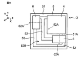
- FIG. 1 is a longitudinal sectional view illustrating a schematic configuration of an article with an RFID tag including the RFID tag according to the embodiment of the present invention.
- FIG. 2 is a bottom view of the RFID tag of FIG.
- an article 1 with an RFID (Radio-Frequency IDentification) tag includes an article 2 having a metal surface 2A and an RFID tag 3 attached to the metal surface 2A.
- the RFID tag 3 is electrically attached to the metal surface 2A via, for example, solder or an anisotropic conductive paste (ACP) or by capacitive coupling.
- the RFID tag 3 includes an RFIC (Radio-Frequency Integrated Circuit) element 4, a first inductor element 5, and two second inductor elements 6.
- RFIC Radio-Frequency Integrated Circuit
- the RFIC element 4 is a chip-shaped component that processes a transmission / reception signal of a predetermined frequency (for example, UHF band, HF band).
- the RFIC element 4 is an RFIC chip corresponding to a communication frequency in the UHF band (860 MHz to 960 MHz).
- the RFIC element 4 in plan view (when viewed from the Z direction), has a size included in the first inductor element 5, that is, a size smaller than the first inductor element 5.
- the RFIC element 4 has, for example, a size of 0.45 mm in the X direction, 0.45 mm in the Y direction, and 0.1 mm in the Z direction.
- the RFID element 4 is electrically attached to the first inductor element 5 via, for example, solder or an anisotropic conductive paste (ACP).
- ACP anisotropic conductive paste
- the first inductor element 5 includes a first insulating substrate 51 and a first coiled antenna 52 built in the first insulating substrate 51.
- the first inductor element 5 is a chip-shaped component (chip inductor).
- the first insulating substrate 51 is a substrate that has a mounting surface 51A that faces the metal surface 2A at a position distant from the metal surface 2A and on which the RFIC element 4 is mounted.
- the first insulating substrate 51 is configured by a laminate in which a plurality of dielectric layers or magnetic layers are laminated.
- the first insulating substrate 51 is, for example, a ceramic laminate.
- the first insulating substrate 51 has, for example, a size of 1.2 mm in the X direction, 1.2 mm in the Y direction, and 0.2 mm in the Z direction.
- the first coiled antenna 52 is a linear antenna conductor wound in a coil around the winding axis 52A.
- the first coiled antenna 52 is an antenna that performs wireless communication in the UHF band.
- the first coiled antenna 52 has a winding axis 52A in a direction (Z direction) orthogonal or substantially orthogonal to the mounting surface 51A.
- a part of the RFIC element 4 is located in the opening area 52B of the first coiled antenna 52.
- the first coiled antenna 52 has, for example, a size of 0.8 mm in the X direction, 0.8 mm in the Y direction, and 0.164 mm in the Z direction.
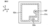
- FIGS. 3A to 3C are bottom views showing a configuration example of the first inductor element 5.
- FIG. 3A to 3C are bottom views showing a configuration example of the first inductor element 5.
- the first insulating substrate 51 is formed by stacking three layers 51a, 51b, and 51c shown in FIGS. 3A to 3C.
- the first coiled antenna 52 is constituted by a laminated coiled antenna in which coil conductor patterns 52a, 52b, 52c formed on the respective layers 51a, 51b, 51c are connected by interlayer connection conductors 52d, 52e, 52f.
- One end of the first coiled antenna 52 is electrically connected to one input / output terminal (not shown) of the RFIC element 4.
- the other end of the first coiled antenna 52 is electrically connected to the other input / output terminal (not shown) of the RFIC element 4.
- two second inductor elements 6 are mounted on the mounting surface 51 ⁇ / b> A of the first insulating substrate 51.
- the RFIC element 4 and the two second inductor elements 6 are arranged on the mounting surface 51A with an interval (for example, 0.125 mm or more) therebetween.
- the second inductor element 6 in plan view (when viewed from the Z direction), has a size included in the first inductor element 5, that is, a size smaller than the first inductor element 5. ing.
- the second inductor element 6 is electrically attached to the first inductor element 5 via, for example, solder or an anisotropic conductive paste (ACP).
- the height (length in the Z direction) of the second inductor element 6 from the mounting surface 51A is designed to be higher than the height of the RFIC element 4 from the mounting surface 51A.
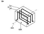
- FIG. 4 is a perspective view showing the inside of the second inductor element 6 in a see-through manner.
- the second inductor element 6 includes a second insulating substrate 61 and a second coiled antenna 62 built in the second insulating substrate 61.
- the second inductor element 6 is a chip-shaped component (chip inductor).
- the second insulating substrate 61 is a substrate mounted on the mounting surface 51A of the first insulating substrate 51.
- the second insulating substrate 61 is configured by a laminate in which a plurality of dielectric layers or magnetic layers are laminated.
- the second insulating substrate 61 is, for example, a ceramic laminate.
- the second insulating substrate 61 has, for example, a size of 0.2 mm in the X direction, 0.4 mm in the Y direction, and 0.3 mm in the Z direction.
- the second coiled antenna 62 is a linear antenna conductor wound in a coil around the winding axis 62A.
- the second coiled antenna 62 is an antenna that performs wireless communication in the UHF band.
- the second coiled antenna 62 has a winding axis 62A parallel or substantially parallel to the mounting surface 51A.
- the two second inductor elements 6 are arranged such that the winding axes 62A of the second coiled antennas 62 intersect (for example, orthogonally).
- one second coiled antenna 62 has a winding axis 62A in the X direction.
- the other second coiled antenna 62 has a winding axis 62A in the Y direction. As shown in FIG.
- the second coiled antenna 62 having the winding axis 62A in the Y direction has, for example, a length in the X direction of 0.35 mm, a length in the Y direction of 0.15 mm, and a length in the Z direction of 0.25 mm. It has the size of
- the second coiled antenna 62 is electrically connected to the first coiled antenna 52.
- one linear antenna conductor forms the first coil antenna 52 and the two second coil antennas 62.
- the configuration is such that two second coiled antennas 62 are inserted into a part of the first coiled antenna 52.
- a resin member 7 is formed on the mounting surface 51A of the first insulating substrate 51 so as to seal the RFIC element 4 and the second inductor element 6, as shown in FIG.
- the resin member 7 prevents the mounting portion of the RFIC element 4 and the second inductor element 6 and the first insulating substrate 51 from being wetted by water and causes a problem such as a short circuit, and also improves the strength of the RFID tag 3. ing.
- FIG. 5 is an equivalent circuit diagram of the RFID tag 3.
- the RFIC element 4 functions as the power supply unit 8 that supplies power
- the first coil antenna 52 functions as the inductor L1
- the second coil antenna 62 functions as the inductor L2.
- the internal capacitance of the RFIC element 4, the first insulating substrate 51, and the second insulating substrate 61 functions as a capacitor C.
- an LC parallel resonance circuit is configured.
- FIG. 6 is a side view showing how wireless communication is performed between the RFID tag 3 and the reader / writer 10 of the RFID system.
- the RFID system is a system for transmitting information between the RFID tag 3 and the reader / writer 10 in a non-contact manner.
- the RFID tag 3 transmits and receives a UHF band high-frequency signal to and from the reader / writer 10.
- the reader / writer 10 includes an antenna 10A formed of a loop conductor.
- the current flowing through the first coiled antenna 52 and the second coiled antenna 62 is supplied to the RFIC element 4, and the RFIC element 4 operates.
- the response signal from the RFIC element 4 is radiated as a magnetic field from the first coil antenna 52 and the second coil antenna 62 and read by the antenna 10A of the reader / writer 10.
- the UHF band high-frequency signal radiated from the antenna 10A causes An eddy current is generated on the metal surface 2A.
- a magnetic field generated by the eddy current as shown by a solid arrow in FIG. 8 can be received by at least one of the second coiled antennas 62 of the two second inductor elements 6.
- the communication distance due to the metal surface 2A is further reduced. Can be suppressed. That is, since the winding axis 62A of the second coiled antenna 62 is provided in parallel or substantially parallel to the mounting surface 51A, the magnetic field flowing in the winding axis direction through the opening area 62B of the second coiled antenna 62 is formed. The influence of the metal surface 2A can be suppressed. Further, since the first inductor element 5 is disposed apart from the metal surface 2A, the influence from the metal surface 2A can be suppressed.
- the first insulating substrate 51 is formed of a laminated body
- the first coiled antenna 52 is formed of a laminated coiled antenna.
- a strong magnetic field can be easily generated.
- the first coiled antenna 52 and the second coiled antenna 62 can operate more effectively. As a result, a decrease in the communication distance due to the metal surface 2A can be further suppressed.
- the winding axis 62A of the second coiled antenna 62 is provided parallel or substantially parallel to the mounting surface 51A. Thereby, it is possible to suppress the flow of the magnetic flux passing through the opening region 62B of the second coiled antenna 62 in the winding axis direction from being hindered by the metal surface 2A. Further, the second coiled antenna 62 can receive a magnetic field due to an eddy current generated on the metal surface 2A by a high-frequency signal radiated from the antenna 10A of the reader / writer 10.
- the antenna 10A of the reader / writer 10 and the RFID tag 3 can communicate with each other.
- the present embodiment when viewed from the winding axis direction (Z direction) of the first coiled antenna 52, a part of the RFIC element 4 and the second inductor element 6 is formed by the opening of the first coiled antenna 52. It is located in the area 52B. Thereby, the size of the RFID tag 3 can be reduced.
- the RFIC element 4 and the second inductor element 6 are arranged on the mounting surface 51A with an interval therebetween. Accordingly, the magnetic field that flows in the opening area 52B of the first coiled antenna 52 in the winding axis direction and is reflected on the RFIC element 4 can flow to the opening area 62B of the second coiled antenna 62. As a result, the second coiled antenna 62 can be made to act more effectively, and the communication distance of the RFID tag 3 can be made longer.
- the two second inductor elements 6 are mounted on the mounting surface 51A, and are arranged such that the winding axis directions of the second coiled antennas 62 intersect each other.
- the magnetic field due to the eddy current generated on the metal surface 2A can be more reliably received by any of the second coiled antennas 62.
- the second coiled antenna 62 can be made to act more effectively, and the communication distance of the RFID tag 3 can be made longer.
- the height of the second inductor element 6 from the mounting surface 51A is designed to be higher than the height of the RFIC element 4 from the mounting surface 51A. Therefore, it is possible to suppress the RFIC element 4 from obstructing the flow of the magnetic field due to the eddy current generated on the metal surface 2A to the opening region 62B of the second coiled antenna 62.
- the resin member 7 is formed on the mounting surface 51A of the first insulating substrate 51 so as to seal the RFIC element 4 and the second inductor element 6.
- the resin member 7 is formed on the mounting surface 51A of the first insulating substrate 51 so as to seal the RFIC element 4 and the second inductor element 6.
- the first coiled antenna 52 and the second coiled antenna 62 are radio communication antennas in the UHF band. Thereby, a stronger magnetic field can be more easily generated on the mounting surface 51A side and the opposite surface side (magnetic field arrival direction), and the first coiled antenna 52 and the second coiled antenna 62 act more effectively. be able to. As a result, a decrease in the communication distance due to the metal surface 2A can be further suppressed.
- the present invention is not limited to the above embodiment, but can be implemented in other various modes.
- two second inductor elements 6 are mounted on the mounting surface 51A, but the present invention is not limited to this.
- one or three or more second inductor elements 6 may be mounted on the mounting surface 51A.
- the mounting positions of the RFIC element 4 and the second inductor element 6 are not particularly limited, and can be appropriately changed.
- the two second inductor elements 6 are connected in series to the RFIC element 4, but the present invention is not limited to this.
- two second inductor elements 6 may be connected in parallel to the RFIC element 4.
- the RFIC element 4 and a part of the second inductor element 6 are located in the opening area 52B of the first coiled antenna 52, but the present invention is not limited to this. Not done. For example, when viewed from the Z direction, all of the RFIC element 4 and the second inductor element 6 may or may not be located in the opening area 52B of the first coiled antenna 52.
- the present invention can further suppress a reduction in communication distance due to a metal surface, and thus is useful as an RFID tag used in an RFID system and an article with an RFID tag.
Landscapes
- Engineering & Computer Science (AREA)
- Computer Networks & Wireless Communication (AREA)
- Computer Hardware Design (AREA)
- Microelectronics & Electronic Packaging (AREA)
- Physics & Mathematics (AREA)
- General Physics & Mathematics (AREA)
- Theoretical Computer Science (AREA)
- Details Of Aerials (AREA)
- Near-Field Transmission Systems (AREA)
Abstract
Provided is an RFID tag (3) that can further suppress a decrease in a communication distance due to a metal surface (2A). The RFID tag comprises: an RFIC element (4); a first inductor element (5) including a first insulating substrate (51) having a mounting surface (51A) for mounting the RFIC element and a first coil antenna (52) built in the first insulating substrate and having a winding shaft (52A) in a direction perpendicular or substantially perpendicular to the mounting surface; and a second inductor element (6) including a second insulating substrate (61) mounted on the mounting surface and a second coil antenna (62) built in the second insulating substrate, electrically connected to the first coil antenna, and having a winding shaft (62A) parallel to or substantially parallel to the mounting surface. The first insulating substrate is configured with a laminated body obtained by laminating a plurality of dielectric layers or magnetic layers. The first coil antenna is configured with a laminated coil antenna obtained by connecting conductor patterns for a coil which are formed on each layer of the laminated body through an interlayer connection conductor.
Description
本発明は、RFID(Radio-Frequency IDentification)タグ及びRFID付き物品に関する。
<< The present invention relates to an RFID (Radio-Frequency @ IDentification) tag and an article with RFID.
従来、この種のRFIDタグとして、コイル状アンテナを内蔵する基板の実装面上にRFIC(Radio-Frequency Integrated circuit)素子を実装した構造を有するRFIDタグが知られている。従来のRFIDタグにおいて、コイル状アンテナは、巻回軸が基板の実装面に対して垂直に設けられている。
Conventionally, as this type of RFID tag, an RFID tag having a structure in which an RFIC (Radio-Frequency Integrated Circuit) element is mounted on a mounting surface of a substrate having a coiled antenna built therein is known. In a conventional RFID tag, the winding axis of the coil antenna is provided perpendicular to the mounting surface of the substrate.
このRFIDタグを金属面に取り付けた場合、コイル状アンテナの開口領域を巻回軸方向に通る磁束の流れが金属面に阻害され、RFIDタグの通信距離が短くなる。これに対して、特許文献1には、コイル状アンテナの巻回軸方向の中心が基板の中心よりも金属面から離れるように構成されたRFIDタグが開示されている。特許文献1のRFIDタグによれば、コイル状アンテナを金属面から離して配置することで、金属面からの影響を抑えて、RFIDタグの通信距離の低下を抑えることができる。
(4) When this RFID tag is mounted on a metal surface, the flow of magnetic flux passing through the opening area of the coiled antenna in the direction of the winding axis is obstructed by the metal surface, and the communication distance of the RFID tag is shortened. On the other hand, Patent Literature 1 discloses an RFID tag configured such that the center of the coiled antenna in the winding axis direction is farther from the metal surface than the center of the substrate. According to the RFID tag disclosed in Patent Literature 1, by disposing the coiled antenna away from the metal surface, it is possible to suppress the influence from the metal surface and to suppress a decrease in the communication distance of the RFID tag.
しかしながら、従来のRFIDタグにおいては、金属面による通信距離の低下を抑えるという観点において未だ改善の余地がある。
However, there is still room for improvement in conventional RFID tags in terms of suppressing a reduction in communication distance due to a metal surface.
本発明の目的は、前記課題を解決することにあって、金属面による通信距離の低下を一層抑えることができるRFIDタグ及びRFIDタグ付き物品を提供することにある。
An object of the present invention is to solve the above-described problems and to provide an RFID tag and an article with an RFID tag that can further suppress a decrease in communication distance due to a metal surface.
前記目的を達成するために、本発明の一態様に係るRFIDタグは、
RFIC素子と、
前記RFIC素子を実装する実装面を有する第1絶縁基板と、前記第1絶縁基板に内蔵され、前記実装面に対して直交又は略直交する方向に巻回軸を有する第1コイル状アンテナとを備える第1インダクタ素子と、
前記実装面に実装される第2絶縁基板と、前記第2絶縁基板に内蔵され、前記第1コイル状アンテナに電気的に接続されるとともに、前記実装面に対して平行又は略平行に巻回軸を有する第2コイル状アンテナとを備える第2インダクタ素子と、
を備え、
前記第1絶縁基板は、複数の誘電体層又は磁性体層を積層した積層体で構成され、
前記第1コイル状アンテナは、前記積層体の各層に形成されたコイル用導体パターンを連結した積層コイル状アンテナで構成されている。 In order to achieve the object, an RFID tag according to one embodiment of the present invention includes:
An RFIC element;
A first insulating substrate having a mounting surface on which the RFIC element is mounted, and a first coiled antenna built in the first insulating substrate and having a winding axis in a direction orthogonal or substantially orthogonal to the mounting surface. A first inductor element provided;
A second insulating substrate mounted on the mounting surface; a second insulating substrate built in the second insulating substrate, electrically connected to the first coiled antenna, and wound parallel or substantially parallel to the mounting surface. A second inductor element comprising: a second coiled antenna having an axis;
With
The first insulating substrate is configured by a laminate in which a plurality of dielectric layers or magnetic layers are laminated,
The first coil antenna is configured by a laminated coil antenna in which coil conductor patterns formed on each layer of the laminate are connected.
また、本発明の一態様に係るRFIDタグ付き物品は、
金属面を有する物品と、
前記金属面に取り付けられたRFIDタグと、
を備えるRFIDタグ付き物品であって、
前記RFIDタグは、
RFIC素子と、
前記金属面に対して離れた位置で対向し且つ前記RFIC素子を実装する実装面を有する第1絶縁基板と、前記第1絶縁基板に内蔵され、前記実装面に対して直交又は略直交する方向に巻回軸を有する第1コイル状アンテナとを備える第1インダクタ素子と、
前記実装面に実装される第2絶縁基板と、前記第2絶縁基板に内蔵され、前記第1コイル状アンテナに電気的に接続されるとともに、前記実装面に対して平行又は略平行に巻回軸を有する第2コイル状アンテナとを備える第2インダクタ素子と、
を備え、
前記第1絶縁基板は、複数の誘電体層又は磁性体層を積層した積層体で構成され、
前記第1コイル状アンテナは、前記積層体の各層に形成されたコイル用導体パターンを連結した積層コイル状アンテナで構成されている。 In addition, the article with the RFID tag according to one embodiment of the present invention includes:
An article having a metal surface;
An RFID tag attached to the metal surface;
An article with an RFID tag comprising:
The RFID tag,
An RFIC element;
A first insulating substrate facing the metal surface at a position distant from the metal surface and having a mounting surface on which the RFIC element is mounted; and a direction embedded in the first insulating substrate and orthogonal or substantially orthogonal to the mounting surface. A first inductor element comprising: a first coiled antenna having a winding axis on the first inductor element;
A second insulating substrate mounted on the mounting surface; a second insulating substrate built in the second insulating substrate, electrically connected to the first coiled antenna, and wound parallel or substantially parallel to the mounting surface. A second inductor element comprising: a second coiled antenna having an axis;
With
The first insulating substrate is configured by a laminate in which a plurality of dielectric layers or magnetic layers are laminated,
The first coil antenna is configured by a laminated coil antenna in which coil conductor patterns formed on each layer of the laminate are connected.
本発明によれば、金属面による通信距離の低下を一層抑えることができる。
According to the present invention, a reduction in the communication distance due to the metal surface can be further suppressed.
本発明の一態様に係るRFIDタグは、
RFIC素子と、
前記RFIC素子を実装する実装面を有する第1絶縁基板と、前記第1絶縁基板に内蔵され、前記実装面に対して直交又は略直交する方向に巻回軸を有する第1コイル状アンテナとを備える第1インダクタ素子と、
前記実装面に実装される第2絶縁基板と、前記第2絶縁基板に内蔵され、前記第1コイル状アンテナに電気的に接続されるとともに、前記実装面に対して平行又は略平行に巻回軸を有する第2コイル状アンテナとを備える第2インダクタ素子と、
を備え、
前記第1絶縁基板は、複数の誘電体層又は磁性体層を積層した積層体で構成され、
前記第1コイル状アンテナは、前記積層体の各層に形成されたコイル用導体パターンを連結した積層コイル状アンテナで構成されている。 An RFID tag according to one embodiment of the present invention includes:
An RFIC element;
A first insulating substrate having a mounting surface on which the RFIC element is mounted, and a first coiled antenna built in the first insulating substrate and having a winding axis in a direction orthogonal or substantially orthogonal to the mounting surface. A first inductor element provided;
A second insulating substrate mounted on the mounting surface; a second insulating substrate built in the second insulating substrate, electrically connected to the first coiled antenna, and wound parallel or substantially parallel to the mounting surface. A second inductor element comprising: a second coiled antenna having an axis;
With
The first insulating substrate is configured by a laminate in which a plurality of dielectric layers or magnetic layers are laminated,
The first coil antenna is configured by a laminated coil antenna in which coil conductor patterns formed on each layer of the laminate are connected.
この構成によれば、金属面に対して第2インダクタ素子が近接し且つ第1インダクタ素子が離れるようにRFIDタグを取り付けることにより、金属面による通信距離の低下を一層抑えることができる。すなわち、第2コイル状アンテナの巻回軸が実装面に対して平行又は略平行に設けられているので、第2コイル状アンテナの開口領域を巻回軸方向に流れる磁界が金属面の影響を受けることを抑えることができる。また、金属面に対して第1インダクタ素子が離れて配置されることにより、金属面からの影響を抑えることができる。さらに、第1絶縁基板を積層体で構成するとともに、第1コイル状アンテナを積層コイル状アンテナで構成することにより、実装面側及びその反対面側(磁界到来方向)により強い磁界を発生させ易くすることができる。これにより、第1コイル状アンテナ及び第2コイル状アンテナをより効果的に作用させることができる。その結果、金属面による通信距離の低下を一層抑えることができる。また、第2コイル状アンテナの巻回軸が実装面に対して平行又は略平行に設けられているので、例えば、リーダライタのアンテナから放射された高周波信号により金属面に発生した渦電流による磁界を第2コイル状アンテナが受けることができる。これにより、リーダライタのアンテナの開口領域と第1コイル状アンテナの開口領域とが重なっていなくても、リーダライタのアンテナとRFIDタグとが通信することができる。
According to this configuration, by mounting the RFID tag such that the second inductor element is close to the metal surface and the first inductor element is separated from the metal surface, it is possible to further suppress a reduction in the communication distance due to the metal surface. That is, since the winding axis of the second coiled antenna is provided parallel or substantially parallel to the mounting surface, the magnetic field flowing in the direction of the winding axis through the opening area of the second coiled antenna is not affected by the metal surface. Can be reduced. Further, since the first inductor element is arranged away from the metal surface, the influence from the metal surface can be suppressed. Furthermore, by forming the first insulating substrate with a laminated body and configuring the first coiled antenna with a laminated coiled antenna, it is easy to generate a strong magnetic field on the mounting surface side and the opposite surface side (magnetic field arrival direction). can do. Thereby, the first coiled antenna and the second coiled antenna can operate more effectively. As a result, a reduction in the communication distance due to the metal surface can be further suppressed. Also, since the winding axis of the second coiled antenna is provided parallel or substantially parallel to the mounting surface, for example, a magnetic field caused by an eddy current generated on a metal surface by a high frequency signal radiated from the antenna of the reader / writer Is received by the second coiled antenna. Thus, even if the opening area of the antenna of the reader / writer does not overlap with the opening area of the first coiled antenna, the antenna of the reader / writer and the RFID tag can communicate with each other.
なお、前記第1コイル状アンテナの巻回軸方向から見て、前記RFIC素子及び第2インダクタ素子の少なくとも一部は、前記第1コイル状アンテナの開口領域内に位置してもよい。この構造によれば、RFIDタグの小型化を図ることができる。
In addition, at least a part of the RFIC element and the second inductor element may be located in the opening area of the first coiled antenna when viewed from the direction of the winding axis of the first coiled antenna. According to this structure, the size of the RFID tag can be reduced.
また、前記RFIC素子と前記第2インダクタ素子とは、互いに間隔を空けて前記実装面に配置されてもよい。この構成によれば、第1コイル状アンテナの開口領域を巻回軸方向に流れてRFIC素子に当たって反射した磁界が第2コイル状アンテナの開口領域へ流れることが可能になる。その結果、第2コイル状アンテナをより効果的に作用させ、RFIDタグの通信距離をより長くすることができる。
In addition, the RFIC element and the second inductor element may be arranged on the mounting surface at an interval from each other. According to this configuration, it is possible for the magnetic field that flows in the opening area of the first coiled antenna in the winding axis direction and is reflected on the RFIC element to flow to the opening area of the second coiled antenna. As a result, it is possible to make the second coil antenna work more effectively, and to make the communication distance of the RFID tag longer.
また、前記実装面には、複数の前記第2インダクタ素子が実装され、前記複数の第2インダクタ素子は、それらの第2コイル状アンテナの巻回軸方向が互いに交差するように配置されてもよい。この構成によれば、金属面に発生した渦電流による磁界を、いずれかの第2コイル状アンテナでより確実に受けることができる。その結果、第2コイル状アンテナをより効果的に作用させ、RFIDタグの通信距離をより長くすることができる。
Also, the plurality of second inductor elements may be mounted on the mounting surface, and the plurality of second inductor elements may be arranged such that the winding axis directions of the second coiled antennas cross each other. Good. According to this configuration, the magnetic field due to the eddy current generated on the metal surface can be more reliably received by any of the second coiled antennas. As a result, it is possible to make the second coil antenna work more effectively, and to make the communication distance of the RFID tag longer.
また、前記第2インダクタ素子の前記実装面からの高さは、前記RFIC素子の前記実装面からの高さよりも高くてもよい。この構成によれば、金属面に発生した渦電流による磁界が第2コイル状アンテナの開口領域へ流れることを、RFIC素子が阻害するのを抑えることができる。
The height of the second inductor element from the mounting surface may be higher than the height of the RFIC element from the mounting surface. According to this configuration, it is possible to suppress the RFIC element from obstructing the flow of the magnetic field due to the eddy current generated on the metal surface to the opening region of the second coiled antenna.
また、前記第1絶縁基板の前記実装面には、前記RFIC素子及び前記第2インダクタ素子を封止するように樹脂部材が形成されてもよい。RFIC素子及び第2インダクタ素子と第1絶縁基板との実装部が水濡れしてショートなどの不具合が生じることを抑えることができるとともに、RFIDタグの強度を向上させることができる。
In addition, a resin member may be formed on the mounting surface of the first insulating substrate so as to seal the RFIC element and the second inductor element. It is possible to suppress the occurrence of problems such as short-circuit due to wetness of the mounting portion of the RFIC element and the second inductor element with the first insulating substrate, and to improve the strength of the RFID tag.
また、前記第1コイル状アンテナ及び前記第2コイル状アンテナは、UHF帯で無線通信するアンテナであってもよい。この構成によれば、実装面側及びその反対面側(磁界到来方向)により強い磁界を一層発生させ易くすることができ、第1コイル状アンテナ及び第2コイル状アンテナをより効果的に作用させることができる。その結果、金属面による通信距離の低下を一層抑えることができる。
The first coil antenna and the second coil antenna may be antennas that perform wireless communication in a UHF band. According to this configuration, a stronger magnetic field can be more easily generated on the mounting surface side and the opposite surface side (magnetic field arrival direction), and the first coil antenna and the second coil antenna operate more effectively. be able to. As a result, a reduction in the communication distance due to the metal surface can be further suppressed.
本発明の一態様に係るRFIDタグ付き物品は、
金属面を有する物品と、
前記金属面に取り付けられたRFIDタグと、
を備えるRFIDタグ付き物品であって、
前記RFIDタグは、
RFIC素子と、
前記金属面に対して離れた位置で対向し且つ前記RFIC素子を実装する実装面を有する第1絶縁基板と、前記第1絶縁基板に内蔵され、前記実装面に対して直交又は略直交する方向に巻回軸を有する第1コイル状アンテナとを備える第1インダクタ素子と、
前記実装面に実装される第2絶縁基板と、前記第2絶縁基板に内蔵され、前記第1コイル状アンテナに電気的に接続されるとともに、前記実装面に対して平行又は略平行に巻回軸を有する第2コイル状アンテナとを備える第2インダクタ素子と、
を備え、
前記第1絶縁基板は、複数の誘電体層又は磁性体層を積層した積層体で構成され、
前記第1コイル状アンテナは、前記積層体の各層に形成された導体パターンを連結した積層コイル状アンテナで構成されている。 Articles with an RFID tag according to one embodiment of the present invention include:
An article having a metal surface;
An RFID tag attached to the metal surface;
An article with an RFID tag comprising:
The RFID tag,
An RFIC element;
A first insulating substrate facing the metal surface at a position distant from the metal surface and having a mounting surface on which the RFIC element is mounted; and a direction embedded in the first insulating substrate and orthogonal or substantially orthogonal to the mounting surface. A first inductor element comprising: a first coiled antenna having a winding axis;
A second insulating substrate mounted on the mounting surface; a second insulating substrate built in the second insulating substrate, electrically connected to the first coiled antenna, and wound parallel or substantially parallel to the mounting surface. A second inductor element comprising: a second coiled antenna having an axis;
With
The first insulating substrate is configured by a laminate in which a plurality of dielectric layers or magnetic layers are laminated,
The first coiled antenna is constituted by a laminated coiled antenna in which conductor patterns formed on each layer of the laminate are connected.
この構成によれば、第1インダクタ素子よりも第2インダクタ素子が金属面に対して近接するようにRFIDタグが取り付けられているので、金属面による通信距離の低下を一層抑えることができる。すなわち、第2コイル状アンテナの巻回軸が実装面に対して平行又は略平行に設けられているので、第2コイル状アンテナの開口領域を巻回軸方向に流れる磁界が金属面の影響を受けることを抑えることができる。また、金属面に対して第1インダクタ素子が離れて配置されることにより、金属面からの影響を抑えることができる。さらに、第1絶縁基板を積層体で構成するとともに、第1コイル状アンテナを積層コイル状アンテナで構成することにより、実装面側及びその反対面側(磁界到来方向)により強い磁界を発生させ易くすることができる。これにより、第1コイル状アンテナ及び第2コイル状アンテナをより効果的に作用させることができる。その結果、金属面による通信距離の低下を一層抑えることができる。また、第2コイル状アンテナの巻回軸が実装面に対して平行又は略平行に設けられているので、第2コイル状アンテナの開口領域を巻回軸方向に通る磁束の流れが金属面によって阻害されることを抑えることができる。また、リーダライタのアンテナから放射された高周波信号により金属面に発生した渦電流による磁界を第2コイル状アンテナが受けることができる。これにより、リーダライタのアンテナの開口領域と第1コイル状アンテナの開口領域とが重なっていなくても、リーダライタのアンテナとRFIDタグとが通信することができる。
According to this configuration, since the RFID tag is attached so that the second inductor element is closer to the metal surface than the first inductor element, it is possible to further suppress a reduction in the communication distance due to the metal surface. That is, since the winding axis of the second coiled antenna is provided parallel or substantially parallel to the mounting surface, the magnetic field flowing in the direction of the winding axis through the opening area of the second coiled antenna is not affected by the metal surface. Can be reduced. Further, since the first inductor element is disposed apart from the metal surface, the influence from the metal surface can be suppressed. Furthermore, by forming the first insulating substrate with a laminated body and configuring the first coiled antenna with a laminated coiled antenna, it is easy to generate a strong magnetic field on the mounting surface side and the opposite surface side (magnetic field arrival direction). can do. Thereby, the first coiled antenna and the second coiled antenna can operate more effectively. As a result, a reduction in the communication distance due to the metal surface can be further suppressed. Further, since the winding axis of the second coiled antenna is provided parallel or substantially parallel to the mounting surface, the flow of magnetic flux passing through the opening area of the second coiled antenna in the winding axis direction is caused by the metal surface. The inhibition can be suppressed. Further, the second coil antenna can receive a magnetic field due to an eddy current generated on the metal surface by a high-frequency signal radiated from the antenna of the reader / writer. Thus, even if the opening area of the antenna of the reader / writer does not overlap with the opening area of the first coiled antenna, the antenna of the reader / writer and the RFID tag can communicate with each other.
以下、本発明の実施形態について、図面を参照しながら説明する。なお、この実施形態によって本発明が限定されるものではない。また、図面において実質的に同一の部材については同一の符号を付している。
Hereinafter, embodiments of the present invention will be described with reference to the drawings. The present invention is not limited by the embodiment. In the drawings, substantially the same members are denoted by the same reference numerals.
(実施形態)
以下、本発明の実施形態に係るRFIDタグ及びRFIDタグ付き物品について説明する。図1は、本発明の実施形態に係るRFIDタグを備えるRFIDタグ付き物品の概略構成を示す縦断面図である。図2は、図1のRFIDタグの底面図であり、一部を透過して示す図である。 (Embodiment)
Hereinafter, an RFID tag and an article with an RFID tag according to an embodiment of the present invention will be described. FIG. 1 is a longitudinal sectional view illustrating a schematic configuration of an article with an RFID tag including the RFID tag according to the embodiment of the present invention. FIG. 2 is a bottom view of the RFID tag of FIG.
図1に示すように、本実施形態に係るRFID(Radio-Frequency IDentification)タグ付き物品1は、金属面2Aを有する物品2と、当該金属面2Aに取り付けられたRFIDタグ3とを備えている。RFIDタグ3は、例えば、はんだや異方性導電ペースト(ACP)を介して、或いは容量結合により電気的に金属面2Aに取り付けられている。
As shown in FIG. 1, an article 1 with an RFID (Radio-Frequency IDentification) tag according to the present embodiment includes an article 2 having a metal surface 2A and an RFID tag 3 attached to the metal surface 2A. . The RFID tag 3 is electrically attached to the metal surface 2A via, for example, solder or an anisotropic conductive paste (ACP) or by capacitive coupling.
RFIDタグ3は、RFIC(Radio-Frequency Integrated Circuit)素子4と、第1インダクタ素子5と、2つの第2インダクタ素子6とを備えている。
The RFID tag 3 includes an RFIC (Radio-Frequency Integrated Circuit) element 4, a first inductor element 5, and two second inductor elements 6.
RFIC素子4は、所定周波数(例えば、UHF帯、HF帯)の送受信信号を処理するチップ状の部品である。本実施形態において、RFIC素子4は、UHF帯(860MHz~960MHz)の通信周波数に対応するRFICチップである。図2に示すように、平面視において(Z方向から見て)、RFIC素子4は、第1インダクタ素子5に包含されるサイズ、すなわち、第1インダクタ素子5よりも小さいサイズを有している。RFIC素子4は、例えば、X方向の長さが0.45mm、Y方向の長さが0.45mm、Z方向の長さ0.1mmのサイズを有している。RFID素子4は、例えば、はんだや異方性導電ペースト(ACP)を介して電気的に第1インダクタ素子5に取り付けられている。
The RFIC element 4 is a chip-shaped component that processes a transmission / reception signal of a predetermined frequency (for example, UHF band, HF band). In the present embodiment, the RFIC element 4 is an RFIC chip corresponding to a communication frequency in the UHF band (860 MHz to 960 MHz). As shown in FIG. 2, in plan view (when viewed from the Z direction), the RFIC element 4 has a size included in the first inductor element 5, that is, a size smaller than the first inductor element 5. . The RFIC element 4 has, for example, a size of 0.45 mm in the X direction, 0.45 mm in the Y direction, and 0.1 mm in the Z direction. The RFID element 4 is electrically attached to the first inductor element 5 via, for example, solder or an anisotropic conductive paste (ACP).
第1インダクタ素子5は、第1絶縁基板51と、第1絶縁基板51に内蔵された第1コイル状アンテナ52とを備えている。本実施形態において、第1インダクタ素子5は、チップ状の部品(チップインダクタ)である。
The first inductor element 5 includes a first insulating substrate 51 and a first coiled antenna 52 built in the first insulating substrate 51. In the present embodiment, the first inductor element 5 is a chip-shaped component (chip inductor).
第1絶縁基板51は、金属面2Aに対して離れた位置で対向し且つRFIC素子4が実装される実装面51Aを有する基板である。本実施形態において、第1絶縁基板51は、複数の誘電体層又は磁性体層を積層した積層体で構成されている。第1絶縁基板51は、例えば、セラミック製の積層体である。第1絶縁基板51は、例えば、X方向の長さが1.2mm、Y方向の長さが1.2mm、Z方向の長さが0.2mmのサイズを有している。
The first insulating substrate 51 is a substrate that has a mounting surface 51A that faces the metal surface 2A at a position distant from the metal surface 2A and on which the RFIC element 4 is mounted. In the present embodiment, the first insulating substrate 51 is configured by a laminate in which a plurality of dielectric layers or magnetic layers are laminated. The first insulating substrate 51 is, for example, a ceramic laminate. The first insulating substrate 51 has, for example, a size of 1.2 mm in the X direction, 1.2 mm in the Y direction, and 0.2 mm in the Z direction.
第1コイル状アンテナ52は、巻回軸52Aを中心としてコイル状に巻き回された線状のアンテナ導体である。本実施形態において、第1コイル状アンテナ52は、UHF帯で無線通信するアンテナである。第1コイル状アンテナ52は、実装面51Aに対して直交又は略直交する方向(Z方向)に巻回軸52Aを有している。図2に示すように、RFIC素子4の一部は、第1コイル状アンテナ52の開口領域52B内に位置している。第1コイル状アンテナ52は、例えば、X方向の長さが0.8mm、Y方向の長さが0.8mm、Z方向の長さ0.164mmのサイズを有している。
The first coiled antenna 52 is a linear antenna conductor wound in a coil around the winding axis 52A. In the present embodiment, the first coiled antenna 52 is an antenna that performs wireless communication in the UHF band. The first coiled antenna 52 has a winding axis 52A in a direction (Z direction) orthogonal or substantially orthogonal to the mounting surface 51A. As shown in FIG. 2, a part of the RFIC element 4 is located in the opening area 52B of the first coiled antenna 52. The first coiled antenna 52 has, for example, a size of 0.8 mm in the X direction, 0.8 mm in the Y direction, and 0.164 mm in the Z direction.
図3A~図3Cは、第1インダクタ素子5の構成例を示す底面図である。
FIGS. 3A to 3C are bottom views showing a configuration example of the first inductor element 5. FIG.
本実施形態において、第1絶縁基板51は、図3A~図3Cに示す3つの層51a,51b,51cを積層して構成されている。第1コイル状アンテナ52は、各層51a,51b,51cに形成されたコイル用導体パターン52a,52b,52cを層間接続導体52d,52e,52fで連結した積層コイル状アンテナで構成されている。第1コイル状アンテナ52の一端部は、RFIC素子4が備える一方の入出力端子(図示せず)に電気的に接続されている。第1コイル状アンテナ52の他端部は、RFIC素子4の他方の入出力端子(図示せず)に電気的に接続されている。
In the present embodiment, the first insulating substrate 51 is formed by stacking three layers 51a, 51b, and 51c shown in FIGS. 3A to 3C. The first coiled antenna 52 is constituted by a laminated coiled antenna in which coil conductor patterns 52a, 52b, 52c formed on the respective layers 51a, 51b, 51c are connected by interlayer connection conductors 52d, 52e, 52f. One end of the first coiled antenna 52 is electrically connected to one input / output terminal (not shown) of the RFIC element 4. The other end of the first coiled antenna 52 is electrically connected to the other input / output terminal (not shown) of the RFIC element 4.
また、図1及び図2に示すように、第1絶縁基板51の実装面51Aには、2つの第2インダクタ素子6が実装されている。本実施形態において、RFIC素子4と2つの第2インダクタ素子6とは、互いに間隔(例えば、0.125mm以上)を空けて実装面51Aに配置されている。図2に示すように、平面視において(Z方向から見て)、第2インダクタ素子6は、第1インダクタ素子5に包含されるサイズ、すなわち、第1インダクタ素子5よりも小さいサイズを有している。第2インダクタ素子6は、例えば、はんだや異方性導電ペースト(ACP)を介して電気的に第1インダクタ素子5に取り付けられている。第2インダクタ素子6の実装面51Aからの高さ(Z方向の長さ)は、RFIC素子4の実装面51Aからの高さよりも高くなるように設計されている。
{Circle around (2)} As shown in FIGS. 1 and 2, two second inductor elements 6 are mounted on the mounting surface 51 </ b> A of the first insulating substrate 51. In the present embodiment, the RFIC element 4 and the two second inductor elements 6 are arranged on the mounting surface 51A with an interval (for example, 0.125 mm or more) therebetween. As shown in FIG. 2, in plan view (when viewed from the Z direction), the second inductor element 6 has a size included in the first inductor element 5, that is, a size smaller than the first inductor element 5. ing. The second inductor element 6 is electrically attached to the first inductor element 5 via, for example, solder or an anisotropic conductive paste (ACP). The height (length in the Z direction) of the second inductor element 6 from the mounting surface 51A is designed to be higher than the height of the RFIC element 4 from the mounting surface 51A.
図4は、第2インダクタ素子6の内部を透過して示す斜視図である。
FIG. 4 is a perspective view showing the inside of the second inductor element 6 in a see-through manner.
図1及び図4に示すように、第2インダクタ素子6は、第2絶縁基板61と、第2絶縁基板61に内蔵された第2コイル状アンテナ62とを備えている。本実施形態において、第2インダクタ素子6は、チップ状の部品(チップインダクタ)である。
及 び As shown in FIGS. 1 and 4, the second inductor element 6 includes a second insulating substrate 61 and a second coiled antenna 62 built in the second insulating substrate 61. In the present embodiment, the second inductor element 6 is a chip-shaped component (chip inductor).
第2絶縁基板61は、第1絶縁基板51の実装面51Aに実装される基板である。本実施形態において、第2絶縁基板61は、複数の誘電体層又は磁性体層を積層した積層体で構成されている。第2絶縁基板61は、例えば、セラミック製の積層体である。第2絶縁基板61は、例えば、X方向の長さが0.2mm、Y方向の長さが0.4mm、Z方向の長さが0.3mmのサイズを有している。
The second insulating substrate 61 is a substrate mounted on the mounting surface 51A of the first insulating substrate 51. In the present embodiment, the second insulating substrate 61 is configured by a laminate in which a plurality of dielectric layers or magnetic layers are laminated. The second insulating substrate 61 is, for example, a ceramic laminate. The second insulating substrate 61 has, for example, a size of 0.2 mm in the X direction, 0.4 mm in the Y direction, and 0.3 mm in the Z direction.
第2コイル状アンテナ62は、巻回軸62Aを中心としてコイル状に巻き回された線状のアンテナ導体である。本実施形態において、第2コイル状アンテナ62は、UHF帯で無線通信するアンテナである。第2コイル状アンテナ62は、実装面51Aに対して平行又は略平行に巻回軸62Aを有している。2つの第2インダクタ素子6は、それらの第2コイル状アンテナ62の巻回軸62Aが互いに交差(例えば、直交)するように配置されている。本実施形態において、一方の第2コイル状アンテナ62は、X方向に巻回軸62Aを有している。他方の第2コイル状アンテナ62は、Y方向に巻回軸62Aを有している。図2に示すように、2つの第2インダクタ素子6のそれぞれの一部は、第1コイル状アンテナ52の開口領域52B内に位置している。Y方向に巻回軸62Aを有している第2コイル状アンテナ62は、例えば、X方向の長さが0.35mm、Y方向の長さが0.15mm、Z方向の長さ0.25mmのサイズを有している。
The second coiled antenna 62 is a linear antenna conductor wound in a coil around the winding axis 62A. In the present embodiment, the second coiled antenna 62 is an antenna that performs wireless communication in the UHF band. The second coiled antenna 62 has a winding axis 62A parallel or substantially parallel to the mounting surface 51A. The two second inductor elements 6 are arranged such that the winding axes 62A of the second coiled antennas 62 intersect (for example, orthogonally). In the present embodiment, one second coiled antenna 62 has a winding axis 62A in the X direction. The other second coiled antenna 62 has a winding axis 62A in the Y direction. As shown in FIG. 2, a part of each of the two second inductor elements 6 is located in the opening area 52 </ b> B of the first coiled antenna 52. The second coiled antenna 62 having the winding axis 62A in the Y direction has, for example, a length in the X direction of 0.35 mm, a length in the Y direction of 0.15 mm, and a length in the Z direction of 0.25 mm. It has the size of
第2コイル状アンテナ62は、第1コイル状アンテナ52に電気的に接続されている。本実施形態においては、1本の線状のアンテナ導体で、第1コイル状アンテナ52と2つの第2コイル状アンテナ62とを構成している。言い換えれば、第1コイル状アンテナ52の一部に2つの第2コイル状アンテナ62が挿入されるように構成されている。
2The second coiled antenna 62 is electrically connected to the first coiled antenna 52. In the present embodiment, one linear antenna conductor forms the first coil antenna 52 and the two second coil antennas 62. In other words, the configuration is such that two second coiled antennas 62 are inserted into a part of the first coiled antenna 52.
また、本実施形態において、第1絶縁基板51の実装面51Aには、図1に示すように、RFIC素子4及び第2インダクタ素子6を封止するように樹脂部材7が形成されている。この樹脂部材7により、RFIC素子4及び第2インダクタ素子6と第1絶縁基板51との実装部が水濡れしてショートなどの不具合が生じることが抑えられるとともに、RFIDタグ3の強度が向上されている。
In the present embodiment, a resin member 7 is formed on the mounting surface 51A of the first insulating substrate 51 so as to seal the RFIC element 4 and the second inductor element 6, as shown in FIG. The resin member 7 prevents the mounting portion of the RFIC element 4 and the second inductor element 6 and the first insulating substrate 51 from being wetted by water and causes a problem such as a short circuit, and also improves the strength of the RFID tag 3. ing.
図5は、RFIDタグ3の等価回路図である。
FIG. 5 is an equivalent circuit diagram of the RFID tag 3.
本実施形態においては、RFIC素子4が電力を供給する給電部8として機能し、第1コイル状アンテナ52がインダクタL1として機能し、第2コイル状アンテナ62がインダクタL2として機能する。また、RFIC素子4、第1絶縁基板51、及び第2絶縁基板61の内部容量がコンデンサCとして機能する。これにより、LC並列共振回路が構成されている。
In the present embodiment, the RFIC element 4 functions as the power supply unit 8 that supplies power, the first coil antenna 52 functions as the inductor L1, and the second coil antenna 62 functions as the inductor L2. Further, the internal capacitance of the RFIC element 4, the first insulating substrate 51, and the second insulating substrate 61 functions as a capacitor C. Thus, an LC parallel resonance circuit is configured.
図6は、RFIDタグ3とRFIDシステムのリーダライタ10との間で無線通信を行う様子を示す側面図である。
FIG. 6 is a side view showing how wireless communication is performed between the RFID tag 3 and the reader / writer 10 of the RFID system.
RFIDシステムは、RFIDタグ3とリーダライタ10との間で、非接触方式で情報を伝達するシステムである。本実施形態において、RFIDタグ3は、リーダライタ10に対してUHF帯の高周波信号の送受信を行う。本実施形態において、リーダライタ10は、ループ状導体で構成されるアンテナ10Aを備えている。
The RFID system is a system for transmitting information between the RFID tag 3 and the reader / writer 10 in a non-contact manner. In the present embodiment, the RFID tag 3 transmits and receives a UHF band high-frequency signal to and from the reader / writer 10. In the present embodiment, the reader / writer 10 includes an antenna 10A formed of a loop conductor.
図6に示すように、リーダライタ10のアンテナ10AをRFIDタグ3に近接させると、アンテナ10Aから放射されたUHF帯の高周波信号に基づく磁界が第1コイル状アンテナ52の開口領域52Bを巻回軸方向(Z方向)に流れる。これにより、第1コイル状アンテナ52に電流が流れる。このとき、金属面2Aに対して第1インダクタ素子5が離れて配置されているので、金属面2Aからの影響を抑えることができる。
As shown in FIG. 6, when the antenna 10A of the reader / writer 10 is brought close to the RFID tag 3, a magnetic field based on the UHF band high-frequency signal radiated from the antenna 10A winds around the opening area 52B of the first coiled antenna 52. It flows in the axial direction (Z direction). As a result, a current flows through the first coiled antenna 52. At this time, since the first inductor element 5 is arranged away from the metal surface 2A, the influence from the metal surface 2A can be suppressed.
また、前記磁界の一部は、図7に示すように、RFIC素子4に当たって反射し、第2コイル状アンテナ62の開口領域62Bへ流れる。これにより、第2コイル状アンテナ62に電流が流れる。このとき、第2コイル状アンテナ62の巻回軸62Aが実装面51Aに対して平行又は略平行に設けられているので、第2コイル状アンテナ62の開口領域62Bを巻回軸方向に流れる磁界が金属面2Aの影響を受けることを抑えることができる。
(7) Further, as shown in FIG. 7, a part of the magnetic field strikes the RFIC element 4 and is reflected and flows to the opening area 62B of the second coiled antenna 62. Thereby, a current flows through the second coiled antenna 62. At this time, since the winding axis 62A of the second coiled antenna 62 is provided parallel or substantially parallel to the mounting surface 51A, the magnetic field flowing in the opening area 62B of the second coiled antenna 62 in the winding axis direction. Can be suppressed from being affected by the metal surface 2A.
第1コイル状アンテナ52及び第2コイル状アンテナ62を流れる電流は、RFIC素子4に供給され、RFIC素子4が動作する。一方、RFIC素子4からの応答信号は第1コイル状アンテナ52及び第2コイル状アンテナ62から磁界として放射され、リーダライタ10のアンテナ10Aで読み取られる。
(4) The current flowing through the first coiled antenna 52 and the second coiled antenna 62 is supplied to the RFIC element 4, and the RFIC element 4 operates. On the other hand, the response signal from the RFIC element 4 is radiated as a magnetic field from the first coil antenna 52 and the second coil antenna 62 and read by the antenna 10A of the reader / writer 10.
また、図8に示すように、リーダライタ10のアンテナ10Aの開口領域10Bと第1コイル状アンテナ52の開口領域52Bとが重なっていないとき、アンテナ10Aから放射されたUHF帯の高周波信号により、金属面2Aに渦電流が発生する。この渦電流によって図8において実線矢印で示すように発生した磁界を、2つの第2インダクタ素子6の少なくとも一方の第2コイル状アンテナ62が受けることができる。
As shown in FIG. 8, when the opening area 10B of the antenna 10A of the reader / writer 10 does not overlap with the opening area 52B of the first coiled antenna 52, the UHF band high-frequency signal radiated from the antenna 10A causes An eddy current is generated on the metal surface 2A. A magnetic field generated by the eddy current as shown by a solid arrow in FIG. 8 can be received by at least one of the second coiled antennas 62 of the two second inductor elements 6.
本実施形態によれば、第1インダクタ素子5よりも第2インダクタ素子6が金属面2Aに対して近接するようにRFIDタグ3が取り付けられているので、金属面2Aによる通信距離の低下を一層抑えることができる。すなわち、第2コイル状アンテナ62の巻回軸62Aが実装面51Aに対して平行又は略平行に設けられているので、第2コイル状アンテナ62の開口領域62Bを巻回軸方向に流れる磁界が金属面2Aの影響を受けることを抑えることができる。また、金属面2Aに対して第1インダクタ素子5が離れて配置されることにより、金属面2Aからの影響を抑えることができる。
According to the present embodiment, since the RFID tag 3 is attached so that the second inductor element 6 is closer to the metal surface 2A than the first inductor element 5, the communication distance due to the metal surface 2A is further reduced. Can be suppressed. That is, since the winding axis 62A of the second coiled antenna 62 is provided in parallel or substantially parallel to the mounting surface 51A, the magnetic field flowing in the winding axis direction through the opening area 62B of the second coiled antenna 62 is formed. The influence of the metal surface 2A can be suppressed. Further, since the first inductor element 5 is disposed apart from the metal surface 2A, the influence from the metal surface 2A can be suppressed.
また、本実施形態によれば、第1絶縁基板51を積層体で構成するとともに、第1コイル状アンテナ52を積層コイル状アンテナで構成することにより、実装面51A側及びその反対面側(磁界到来方向)により強い磁界を発生させ易くすることができる。これにより、第1コイル状アンテナ52及び第2コイル状アンテナ62をより効果的に作用させることができる。その結果、金属面2Aによる通信距離の低下を一層抑えることができる。
Further, according to the present embodiment, the first insulating substrate 51 is formed of a laminated body, and the first coiled antenna 52 is formed of a laminated coiled antenna. A strong magnetic field can be easily generated. Thereby, the first coiled antenna 52 and the second coiled antenna 62 can operate more effectively. As a result, a decrease in the communication distance due to the metal surface 2A can be further suppressed.
また、本実施形態によれば、第2コイル状アンテナ62の巻回軸62Aが実装面51Aに対して平行又は略平行に設けられている。これにより、第2コイル状アンテナ62の開口領域62Bを巻回軸方向に通る磁束の流れが金属面2Aによって阻害されることを抑えることができる。また、リーダライタ10のアンテナ10Aから放射された高周波信号により金属面2Aに発生した渦電流による磁界を第2コイル状アンテナ62が受けることができる。これにより、リーダライタ10のアンテナ10Aの開口領域10Bと第2コイル状アンテナ62の開口領域62Bとが重なっていなくても、リーダライタ10のアンテナ10AとRFIDタグ3とが通信することができる。
According to the present embodiment, the winding axis 62A of the second coiled antenna 62 is provided parallel or substantially parallel to the mounting surface 51A. Thereby, it is possible to suppress the flow of the magnetic flux passing through the opening region 62B of the second coiled antenna 62 in the winding axis direction from being hindered by the metal surface 2A. Further, the second coiled antenna 62 can receive a magnetic field due to an eddy current generated on the metal surface 2A by a high-frequency signal radiated from the antenna 10A of the reader / writer 10. Thus, even if the opening area 10B of the antenna 10A of the reader / writer 10 does not overlap with the opening area 62B of the second coiled antenna 62, the antenna 10A of the reader / writer 10 and the RFID tag 3 can communicate with each other.
また、本実施形態によれば、第1コイル状アンテナ52の巻回軸方向(Z方向)から見て、RFIC素子4及び第2インダクタ素子6の一部は、第1コイル状アンテナ52の開口領域52B内に位置している。これにより、RFIDタグ3の小型化を図ることができる。
Further, according to the present embodiment, when viewed from the winding axis direction (Z direction) of the first coiled antenna 52, a part of the RFIC element 4 and the second inductor element 6 is formed by the opening of the first coiled antenna 52. It is located in the area 52B. Thereby, the size of the RFID tag 3 can be reduced.
また、本実施形態によれば、RFIC素子4と第2インダクタ素子6とが、互いに間隔を空けて実装面51Aに配置されている。これにより、第1コイル状アンテナ52の開口領域52Bを巻回軸方向に流れてRFIC素子4に当たって反射した磁界が第2コイル状アンテナ62の開口領域62Bへ流れることが可能になる。その結果、第2コイル状アンテナ62をより効果的に作用させ、RFIDタグ3の通信距離をより長くすることができる。
According to the present embodiment, the RFIC element 4 and the second inductor element 6 are arranged on the mounting surface 51A with an interval therebetween. Accordingly, the magnetic field that flows in the opening area 52B of the first coiled antenna 52 in the winding axis direction and is reflected on the RFIC element 4 can flow to the opening area 62B of the second coiled antenna 62. As a result, the second coiled antenna 62 can be made to act more effectively, and the communication distance of the RFID tag 3 can be made longer.
また、本実施形態によれば、実装面51Aには、2つの第2インダクタ素子6が実装され、それらの第2コイル状アンテナ62の巻回軸方向が互いに交差するように配置されている。これにより、金属面2Aに発生した渦電流による磁界を、いずれかの第2コイル状アンテナ62でより確実に受けることができる。その結果、第2コイル状アンテナ62をより効果的に作用させ、RFIDタグ3の通信距離をより長くすることができる。
According to the present embodiment, the two second inductor elements 6 are mounted on the mounting surface 51A, and are arranged such that the winding axis directions of the second coiled antennas 62 intersect each other. Thereby, the magnetic field due to the eddy current generated on the metal surface 2A can be more reliably received by any of the second coiled antennas 62. As a result, the second coiled antenna 62 can be made to act more effectively, and the communication distance of the RFID tag 3 can be made longer.
また、本実施形態によれば、第2インダクタ素子6の実装面51Aからの高さは、RFIC素子4の実装面51Aからの高さよりも高く設計されている。これにより、金属面2Aに発生した渦電流による磁界が第2コイル状アンテナ62の開口領域62Bへ流れることを、RFIC素子4が阻害するのを抑えることができる。
According to the present embodiment, the height of the second inductor element 6 from the mounting surface 51A is designed to be higher than the height of the RFIC element 4 from the mounting surface 51A. Thereby, it is possible to suppress the RFIC element 4 from obstructing the flow of the magnetic field due to the eddy current generated on the metal surface 2A to the opening region 62B of the second coiled antenna 62.
また、本実施形態によれば、第1絶縁基板51の実装面51Aには、RFIC素子4及び第2インダクタ素子6を封止するように樹脂部材7が形成されている。これにより、RFIC素子4及び第2インダクタ素子6と第1絶縁基板51との実装部が水濡れしてショートなどの不具合が生じることを抑えることができるとともに、RFIDタグ3の強度を向上させることができる。
According to the present embodiment, the resin member 7 is formed on the mounting surface 51A of the first insulating substrate 51 so as to seal the RFIC element 4 and the second inductor element 6. Thereby, it is possible to suppress a problem such as a short circuit due to wet mounting of the mounting portion of the RFIC element 4, the second inductor element 6, and the first insulating substrate 51, and to improve the strength of the RFID tag 3. Can be.
また、本実施形態によれば、第1コイル状アンテナ52及び第2コイル状アンテナ62は、UHF帯で無線通信するアンテナである。これにより、実装面51A側及びその反対面側(磁界到来方向)により強い磁界を一層発生させ易くすることができ、第1コイル状アンテナ52及び第2コイル状アンテナ62をより効果的に作用させることができる。その結果、金属面2Aによる通信距離の低下を一層抑えることができる。
According to the present embodiment, the first coiled antenna 52 and the second coiled antenna 62 are radio communication antennas in the UHF band. Thereby, a stronger magnetic field can be more easily generated on the mounting surface 51A side and the opposite surface side (magnetic field arrival direction), and the first coiled antenna 52 and the second coiled antenna 62 act more effectively. be able to. As a result, a decrease in the communication distance due to the metal surface 2A can be further suppressed.
なお、本発明は前記実施の形態に限定されるものではなく、その他種々の態様で実施できる。例えば、前記では、実装面51Aに2つの第2インダクタ素子6を実装するようにしたが、本発明はこれに限定されない。例えば、実装面51Aに1つ又は3つ以上の第2インダクタ素子6を実装するようにしてもよい。また、RFIC素子4及び第2インダクタ素子6の実装位置は、特に限定されるものではなく、適宜変更可能である。
The present invention is not limited to the above embodiment, but can be implemented in other various modes. For example, in the above description, two second inductor elements 6 are mounted on the mounting surface 51A, but the present invention is not limited to this. For example, one or three or more second inductor elements 6 may be mounted on the mounting surface 51A. Further, the mounting positions of the RFIC element 4 and the second inductor element 6 are not particularly limited, and can be appropriately changed.
また、前記では、2つの第2インダクタ素子6をRFIC素子4に対して直列に接続するようにしたが、本発明はこれに限定されない。例えば、図9に示すように、2つの第2インダクタ素子6をRFIC素子4に対して並列に接続してもよい。
In the above description, the two second inductor elements 6 are connected in series to the RFIC element 4, but the present invention is not limited to this. For example, as shown in FIG. 9, two second inductor elements 6 may be connected in parallel to the RFIC element 4.
また、前記では、Z方向から見て、RFIC素子4及び第2インダクタ素子6の一部が、第1コイル状アンテナ52の開口領域52B内に位置するものとしたが、本発明はこれに限定されない。例えば、Z方向から見て、RFIC素子4及び第2インダクタ素子6の全部が、第1コイル状アンテナ52の開口領域52B内に位置してもよいし、位置しなくてもよい。
In the above description, when viewed from the Z direction, the RFIC element 4 and a part of the second inductor element 6 are located in the opening area 52B of the first coiled antenna 52, but the present invention is not limited to this. Not done. For example, when viewed from the Z direction, all of the RFIC element 4 and the second inductor element 6 may or may not be located in the opening area 52B of the first coiled antenna 52.
本発明は、添付図面を参照しながら好ましい実施の形態に関連して充分に記載されているが、この技術に熟練した人々にとっては種々の変形や修正は明白である。そのような変形や修正は、添付した請求の範囲による本発明の範囲から外れない限りにおいて、その中に含まれると理解されるべきである。
Although the present invention has been fully described in connection with preferred embodiments thereof with reference to the accompanying drawings, various changes and modifications will be apparent to those skilled in the art. It is to be understood that such changes and modifications are included therein unless they depart from the scope of the invention as set forth in the appended claims.
本発明は、金属面による通信距離の低下を一層抑えることができるので、RFIDシステムに用いるRFIDタグ及びRFIDタグ付き物品として有用である。
The present invention can further suppress a reduction in communication distance due to a metal surface, and thus is useful as an RFID tag used in an RFID system and an article with an RFID tag.
1 RFIDタグ付き物品
2 物品
2A 金属面
3 RFIDタグ
4 RFIC素子
5 第1インダクタ素子
6 第2インダクタ素子
7 樹脂部材
8 給電部
10 リーダライタ
10A アンテナ
10B 開口領域
51 第1絶縁基板
51A 実装面
51a,51b,51c 層
52 第1コイル状アンテナ
52A 巻回軸
52B 開口領域
52a,52b,52c コイル用導体パターン
52d,52e,52f 層間接続導体
61 第2絶縁基板
62 第2コイル状アンテナ
62A 巻回軸
62B 開口領域
L1,L2 インダクタ
C コンデンサ DESCRIPTION OFSYMBOLS 1 Article with RFID tag 2 Article 2A Metal surface 3 RFID tag 4 RFID element 5 First inductor element 6 Second inductor element 7 Resin member 8 Feeding part 10 Reader / writer 10A Antenna 10B Open area 51 First insulating substrate 51A Mounting surface 51a, 51b, 51c layer 52 first coiled antenna 52A winding axis 52B open area 52a, 52b, 52c coil conductor pattern 52d, 52e, 52f interlayer connection conductor 61 second insulating substrate 62 second coiled antenna 62A winding axis 62B Open area L1, L2 Inductor C Capacitor
2 物品
2A 金属面
3 RFIDタグ
4 RFIC素子
5 第1インダクタ素子
6 第2インダクタ素子
7 樹脂部材
8 給電部
10 リーダライタ
10A アンテナ
10B 開口領域
51 第1絶縁基板
51A 実装面
51a,51b,51c 層
52 第1コイル状アンテナ
52A 巻回軸
52B 開口領域
52a,52b,52c コイル用導体パターン
52d,52e,52f 層間接続導体
61 第2絶縁基板
62 第2コイル状アンテナ
62A 巻回軸
62B 開口領域
L1,L2 インダクタ
C コンデンサ DESCRIPTION OF
Claims (8)
- RFIC素子と、
前記RFIC素子を実装する実装面を有する第1絶縁基板と、前記第1絶縁基板に内蔵され、前記実装面に対して直交又は略直交する方向に巻回軸を有する第1コイル状アンテナとを備える第1インダクタ素子と、
前記実装面に実装される第2絶縁基板と、前記第2絶縁基板に内蔵され、前記第1コイル状アンテナに電気的に接続されるとともに、前記実装面に対して平行又は略平行に巻回軸を有する第2コイル状アンテナとを備える第2インダクタ素子と、
を備え、
前記第1絶縁基板は、複数の誘電体層又は磁性体層を積層した積層体で構成され、
前記第1コイル状アンテナは、前記積層体の各層に形成されたコイル用導体パターンを層間接続導体で連結した積層コイル状アンテナで構成されている、RFIDタグ。 An RFIC element;
A first insulating substrate having a mounting surface on which the RFIC element is mounted, and a first coiled antenna built in the first insulating substrate and having a winding axis in a direction orthogonal or substantially orthogonal to the mounting surface. A first inductor element provided;
A second insulating substrate mounted on the mounting surface; a second insulating substrate built in the second insulating substrate, electrically connected to the first coiled antenna, and wound parallel or substantially parallel to the mounting surface. A second inductor element comprising: a second coiled antenna having an axis;
With
The first insulating substrate is configured by a laminate in which a plurality of dielectric layers or magnetic layers are laminated,
An RFID tag, wherein the first coiled antenna is configured by a laminated coiled antenna in which coil conductor patterns formed on each layer of the laminate are connected by interlayer connection conductors. - 前記第1コイル状アンテナの巻回軸方向から見て、前記RFIC素子及び第2インダクタ素子の少なくとも一部は、前記第1コイル状アンテナの開口領域内に位置する、請求項1に記載のRFIDタグ。 The RFID according to claim 1, wherein at least a part of the RFIC element and the second inductor element are located in an opening area of the first coiled antenna when viewed from a direction of a winding axis of the first coiled antenna. tag.
- 前記RFIC素子と前記第2インダクタ素子とは、互いに間隔を空けて前記実装面に配置されている、請求項2に記載のRFIDタグ。 The RFID tag according to claim 2, wherein the RFIC element and the second inductor element are arranged on the mounting surface with an interval therebetween.
- 前記実装面には、複数の前記第2インダクタ素子が実装され、
前記複数の第2インダクタ素子は、それらの第2コイル状アンテナの巻回軸方向が互いに交差するように配置されている、請求項1~3のいずれか1つに記載のRFIDタグ。 A plurality of the second inductor elements are mounted on the mounting surface,
The RFID tag according to any one of claims 1 to 3, wherein the plurality of second inductor elements are arranged such that the winding axis directions of the second coiled antennas cross each other. - 前記第2インダクタ素子の前記実装面からの高さは、前記RFIC素子の前記実装面からの高さよりも高い、請求項1~4のいずれか1つに記載のRFIDタグ。 The RFID tag according to any one of claims 1 to 4, wherein the height of the second inductor element from the mounting surface is higher than the height of the RFIC element from the mounting surface.
- 前記第1絶縁基板の前記実装面には、前記RFIC素子及び前記第2インダクタ素子を封止するように樹脂部材が形成されている、請求項1~5のいずれか1つに記載のRFIDタグ。 The RFID tag according to any one of claims 1 to 5, wherein a resin member is formed on the mounting surface of the first insulating substrate so as to seal the RFIC element and the second inductor element. .
- 前記第1コイル状アンテナ及び前記第2コイル状アンテナは、UHF帯で無線通信するアンテナである、請求項1~6のいずれか1つに記載のRFIDタグ。 The RFID tag according to any one of claims 1 to 6, wherein the first coil antenna and the second coil antenna are antennas that perform wireless communication in a UHF band.
- 金属面を有する物品と、
前記金属面に取り付けられたRFIDタグと、
を備えるRFIDタグ付き物品であって、
前記RFIDタグは、
RFIC素子と、
前記金属面に対して離れた位置で対向し且つ前記RFIC素子を実装する実装面を有する第1絶縁基板と、前記第1絶縁基板に内蔵され、前記実装面に対して直交又は略直交する方向に巻回軸を有する第1コイル状アンテナとを備える第1インダクタ素子と、
前記実装面に実装される第2絶縁基板と、前記第2絶縁基板に内蔵され、前記第1コイル状アンテナに電気的に接続されるとともに、前記実装面に対して平行又は略平行に巻回軸を有する第2コイル状アンテナとを備える第2インダクタ素子と、
を備え、
前記第1絶縁基板は、複数の誘電体層又は磁性体層を積層した積層体で構成され、
前記第1コイル状アンテナは、前記積層体の各層に形成されたコイル用導体パターンを層間接続導体で連結した積層コイル状アンテナで構成されている、RFIDタグ付き物品。 An article having a metal surface;
An RFID tag attached to the metal surface;
An article with an RFID tag comprising:
The RFID tag,
An RFIC element;
A first insulating substrate facing the metal surface at a position distant from the metal surface and having a mounting surface on which the RFIC element is mounted; and a direction embedded in the first insulating substrate and orthogonal or substantially orthogonal to the mounting surface. A first inductor element comprising: a first coiled antenna having a winding axis;
A second insulating substrate mounted on the mounting surface; a second insulating substrate built in the second insulating substrate, electrically connected to the first coiled antenna, and wound parallel or substantially parallel to the mounting surface. A second inductor element comprising: a second coiled antenna having an axis;
With
The first insulating substrate is configured by a laminate in which a plurality of dielectric layers or magnetic layers are laminated,
An article with an RFID tag, wherein the first coiled antenna is constituted by a laminated coiled antenna in which coil conductor patterns formed on each layer of the laminate are connected by interlayer connection conductors.
Priority Applications (4)
| Application Number | Priority Date | Filing Date | Title |
|---|---|---|---|
| EP19732530.1A EP3611670B8 (en) | 2018-06-25 | 2019-01-23 | Rfid tag and rfid tagged article |
| CN201980000999.0A CN110859048B (en) | 2018-06-25 | 2019-01-23 | RFID tag and article with RFID tag |
| JP2019521847A JP6590119B1 (en) | 2018-06-25 | 2019-01-23 | RFID tag and article with RFID |
| US16/455,859 US11138491B2 (en) | 2018-06-25 | 2019-06-28 | RFID tag and RFID tagged article |
Applications Claiming Priority (2)
| Application Number | Priority Date | Filing Date | Title |
|---|---|---|---|
| JP2018120101 | 2018-06-25 | ||
| JP2018-120101 | 2018-06-25 |
Related Child Applications (1)
| Application Number | Title | Priority Date | Filing Date |
|---|---|---|---|
| US16/455,859 Continuation US11138491B2 (en) | 2018-06-25 | 2019-06-28 | RFID tag and RFID tagged article |
Publications (1)
| Publication Number | Publication Date |
|---|---|
| WO2020003568A1 true WO2020003568A1 (en) | 2020-01-02 |
Family
ID=67437487
Family Applications (1)
| Application Number | Title | Priority Date | Filing Date |
|---|---|---|---|
| PCT/JP2019/002003 WO2020003568A1 (en) | 2018-06-25 | 2019-01-23 | Rfid tag and rfid attached material |
Country Status (2)
| Country | Link |
|---|---|
| CN (1) | CN110859048B (en) |
| WO (1) | WO2020003568A1 (en) |
Citations (4)
| Publication number | Priority date | Publication date | Assignee | Title |
|---|---|---|---|---|
| JPH11297520A (en) * | 1998-04-08 | 1999-10-29 | Mitsubishi Materials Corp | Burglarproof tag and its manufacture |
| JP2012201596A (en) | 2011-03-23 | 2012-10-22 | National Agriculture & Food Research Organization | Nematode resistance-inducing agent and nematode control method |
| WO2013115158A1 (en) * | 2012-02-01 | 2013-08-08 | 株式会社村田製作所 | Antenna device and wireless communication device |
| JP2014064267A (en) * | 2012-08-27 | 2014-04-10 | Tdk Corp | Antenna device |
Family Cites Families (5)
| Publication number | Priority date | Publication date | Assignee | Title |
|---|---|---|---|---|
| GB2491447B (en) * | 2010-03-24 | 2014-10-22 | Murata Manufacturing Co | RFID system |
| JP5062382B2 (en) * | 2010-09-07 | 2012-10-31 | 株式会社村田製作所 | Antenna device |
| JP5293907B2 (en) * | 2011-06-13 | 2013-09-18 | 株式会社村田製作所 | Antenna device and communication terminal device |
| CN204991962U (en) * | 2014-02-14 | 2016-01-20 | 株式会社村田制作所 | Antenna device, and wireless communication device |
| JP2016170808A (en) * | 2016-06-03 | 2016-09-23 | 株式会社村田製作所 | Radio ic tag and rfid system |
-
2019
- 2019-01-23 CN CN201980000999.0A patent/CN110859048B/en active Active
- 2019-01-23 WO PCT/JP2019/002003 patent/WO2020003568A1/en unknown
Patent Citations (4)
| Publication number | Priority date | Publication date | Assignee | Title |
|---|---|---|---|---|
| JPH11297520A (en) * | 1998-04-08 | 1999-10-29 | Mitsubishi Materials Corp | Burglarproof tag and its manufacture |
| JP2012201596A (en) | 2011-03-23 | 2012-10-22 | National Agriculture & Food Research Organization | Nematode resistance-inducing agent and nematode control method |
| WO2013115158A1 (en) * | 2012-02-01 | 2013-08-08 | 株式会社村田製作所 | Antenna device and wireless communication device |
| JP2014064267A (en) * | 2012-08-27 | 2014-04-10 | Tdk Corp | Antenna device |
Also Published As
| Publication number | Publication date |
|---|---|
| CN110859048A (en) | 2020-03-03 |
| CN110859048B (en) | 2023-11-10 |
Similar Documents
| Publication | Publication Date | Title |
|---|---|---|
| JP3148168U (en) | Wireless IC device | |
| US9847578B2 (en) | Antenna device and communication terminal apparatus | |
| JP5267463B2 (en) | Wireless IC device and wireless communication system | |
| JP5299518B2 (en) | Information processing system | |
| US8668151B2 (en) | Wireless IC device | |
| US8177138B2 (en) | Radio IC device | |
| KR101374302B1 (en) | Antenna device and communication terminal device | |
| US8602310B2 (en) | Radio communication device and radio communication terminal | |
| US9825361B2 (en) | Antenna with multifrequency capability for miniaturized applications | |
| EP2385580B1 (en) | Antenna and wireless ic device | |
| WO2012005278A1 (en) | Antenna and rfid device | |
| JP5240050B2 (en) | Coupling substrate, electromagnetic coupling module, and wireless IC device | |
| US10476147B2 (en) | Antenna device and method of manufacturing the same | |
| WO2012141070A1 (en) | Wireless ic device and wireless communication terminal | |
| US20120086526A1 (en) | Wireless ic device and coupling method for power feeding circuit and radiation plate | |
| US9846834B2 (en) | Antenna device and wireless communication device | |
| JP2012161062A (en) | Antenna and rfid device | |
| WO2020003568A1 (en) | Rfid tag and rfid attached material | |
| JP6590119B1 (en) | RFID tag and article with RFID | |
| JP6555320B2 (en) | Wireless IC tag and RFID system | |
| JP5983724B2 (en) | Wireless IC tag and RFID system | |
| WO2019239626A1 (en) | Rfid tag and method for producing same |
Legal Events
| Date | Code | Title | Description |
|---|---|---|---|
| ENP | Entry into the national phase |
Ref document number: 2019521847 Country of ref document: JP Kind code of ref document: A |
|
| ENP | Entry into the national phase |
Ref document number: 2019732530 Country of ref document: EP Effective date: 20190726 |
|
| 121 | Ep: the epo has been informed by wipo that ep was designated in this application |
Ref document number: 19732530 Country of ref document: EP Kind code of ref document: A1 |
|
| NENP | Non-entry into the national phase |
Ref country code: DE |