WO2020000091A1 - Modular multi-level dc/dc converter with current-shaping - Google Patents
Modular multi-level dc/dc converter with current-shaping Download PDFInfo
- Publication number
- WO2020000091A1 WO2020000091A1 PCT/CA2019/050880 CA2019050880W WO2020000091A1 WO 2020000091 A1 WO2020000091 A1 WO 2020000091A1 CA 2019050880 W CA2019050880 W CA 2019050880W WO 2020000091 A1 WO2020000091 A1 WO 2020000091A1
- Authority
- WO
- WIPO (PCT)
- Prior art keywords
- voltage
- csm
- vsm
- current
- network
- Prior art date
- Legal status (The legal status is an assumption and is not a legal conclusion. Google has not performed a legal analysis and makes no representation as to the accuracy of the status listed.)
- Ceased
Links
Classifications
-
- H—ELECTRICITY
- H02—GENERATION; CONVERSION OR DISTRIBUTION OF ELECTRIC POWER
- H02M—APPARATUS FOR CONVERSION BETWEEN AC AND AC, BETWEEN AC AND DC, OR BETWEEN DC AND DC, AND FOR USE WITH MAINS OR SIMILAR POWER SUPPLY SYSTEMS; CONVERSION OF DC OR AC INPUT POWER INTO SURGE OUTPUT POWER; CONTROL OR REGULATION THEREOF
- H02M1/00—Details of apparatus for conversion
- H02M1/14—Arrangements for reducing ripples from DC input or output
- H02M1/15—Arrangements for reducing ripples from DC input or output using active elements
-
- H—ELECTRICITY
- H02—GENERATION; CONVERSION OR DISTRIBUTION OF ELECTRIC POWER
- H02M—APPARATUS FOR CONVERSION BETWEEN AC AND AC, BETWEEN AC AND DC, OR BETWEEN DC AND DC, AND FOR USE WITH MAINS OR SIMILAR POWER SUPPLY SYSTEMS; CONVERSION OF DC OR AC INPUT POWER INTO SURGE OUTPUT POWER; CONTROL OR REGULATION THEREOF
- H02M1/00—Details of apparatus for conversion
- H02M1/08—Circuits specially adapted for the generation of control voltages for semiconductor devices incorporated in static converters
-
- H—ELECTRICITY
- H02—GENERATION; CONVERSION OR DISTRIBUTION OF ELECTRIC POWER
- H02M—APPARATUS FOR CONVERSION BETWEEN AC AND AC, BETWEEN AC AND DC, OR BETWEEN DC AND DC, AND FOR USE WITH MAINS OR SIMILAR POWER SUPPLY SYSTEMS; CONVERSION OF DC OR AC INPUT POWER INTO SURGE OUTPUT POWER; CONTROL OR REGULATION THEREOF
- H02M1/00—Details of apparatus for conversion
- H02M1/12—Arrangements for reducing harmonics from AC input or output
-
- H—ELECTRICITY
- H02—GENERATION; CONVERSION OR DISTRIBUTION OF ELECTRIC POWER
- H02M—APPARATUS FOR CONVERSION BETWEEN AC AND AC, BETWEEN AC AND DC, OR BETWEEN DC AND DC, AND FOR USE WITH MAINS OR SIMILAR POWER SUPPLY SYSTEMS; CONVERSION OF DC OR AC INPUT POWER INTO SURGE OUTPUT POWER; CONTROL OR REGULATION THEREOF
- H02M3/00—Conversion of DC power input into DC power output
- H02M3/02—Conversion of DC power input into DC power output without intermediate conversion into AC
- H02M3/04—Conversion of DC power input into DC power output without intermediate conversion into AC by static converters
- H02M3/10—Conversion of DC power input into DC power output without intermediate conversion into AC by static converters using discharge tubes with control electrode or semiconductor devices with control electrode
- H02M3/145—Conversion of DC power input into DC power output without intermediate conversion into AC by static converters using discharge tubes with control electrode or semiconductor devices with control electrode using devices of a triode or transistor type requiring continuous application of a control signal
- H02M3/155—Conversion of DC power input into DC power output without intermediate conversion into AC by static converters using discharge tubes with control electrode or semiconductor devices with control electrode using devices of a triode or transistor type requiring continuous application of a control signal using semiconductor devices only
- H02M3/156—Conversion of DC power input into DC power output without intermediate conversion into AC by static converters using discharge tubes with control electrode or semiconductor devices with control electrode using devices of a triode or transistor type requiring continuous application of a control signal using semiconductor devices only with automatic control of output voltage or current, e.g. switching regulators
- H02M3/157—Conversion of DC power input into DC power output without intermediate conversion into AC by static converters using discharge tubes with control electrode or semiconductor devices with control electrode using devices of a triode or transistor type requiring continuous application of a control signal using semiconductor devices only with automatic control of output voltage or current, e.g. switching regulators with digital control
-
- H—ELECTRICITY
- H02—GENERATION; CONVERSION OR DISTRIBUTION OF ELECTRIC POWER
- H02M—APPARATUS FOR CONVERSION BETWEEN AC AND AC, BETWEEN AC AND DC, OR BETWEEN DC AND DC, AND FOR USE WITH MAINS OR SIMILAR POWER SUPPLY SYSTEMS; CONVERSION OF DC OR AC INPUT POWER INTO SURGE OUTPUT POWER; CONTROL OR REGULATION THEREOF
- H02M3/00—Conversion of DC power input into DC power output
- H02M3/02—Conversion of DC power input into DC power output without intermediate conversion into AC
- H02M3/04—Conversion of DC power input into DC power output without intermediate conversion into AC by static converters
- H02M3/10—Conversion of DC power input into DC power output without intermediate conversion into AC by static converters using discharge tubes with control electrode or semiconductor devices with control electrode
- H02M3/145—Conversion of DC power input into DC power output without intermediate conversion into AC by static converters using discharge tubes with control electrode or semiconductor devices with control electrode using devices of a triode or transistor type requiring continuous application of a control signal
- H02M3/155—Conversion of DC power input into DC power output without intermediate conversion into AC by static converters using discharge tubes with control electrode or semiconductor devices with control electrode using devices of a triode or transistor type requiring continuous application of a control signal using semiconductor devices only
- H02M3/156—Conversion of DC power input into DC power output without intermediate conversion into AC by static converters using discharge tubes with control electrode or semiconductor devices with control electrode using devices of a triode or transistor type requiring continuous application of a control signal using semiconductor devices only with automatic control of output voltage or current, e.g. switching regulators
- H02M3/158—Conversion of DC power input into DC power output without intermediate conversion into AC by static converters using discharge tubes with control electrode or semiconductor devices with control electrode using devices of a triode or transistor type requiring continuous application of a control signal using semiconductor devices only with automatic control of output voltage or current, e.g. switching regulators including plural semiconductor devices as final control devices for a single load
-
- H—ELECTRICITY
- H02—GENERATION; CONVERSION OR DISTRIBUTION OF ELECTRIC POWER
- H02M—APPARATUS FOR CONVERSION BETWEEN AC AND AC, BETWEEN AC AND DC, OR BETWEEN DC AND DC, AND FOR USE WITH MAINS OR SIMILAR POWER SUPPLY SYSTEMS; CONVERSION OF DC OR AC INPUT POWER INTO SURGE OUTPUT POWER; CONTROL OR REGULATION THEREOF
- H02M3/00—Conversion of DC power input into DC power output
- H02M3/02—Conversion of DC power input into DC power output without intermediate conversion into AC
- H02M3/04—Conversion of DC power input into DC power output without intermediate conversion into AC by static converters
- H02M3/10—Conversion of DC power input into DC power output without intermediate conversion into AC by static converters using discharge tubes with control electrode or semiconductor devices with control electrode
- H02M3/145—Conversion of DC power input into DC power output without intermediate conversion into AC by static converters using discharge tubes with control electrode or semiconductor devices with control electrode using devices of a triode or transistor type requiring continuous application of a control signal
- H02M3/155—Conversion of DC power input into DC power output without intermediate conversion into AC by static converters using discharge tubes with control electrode or semiconductor devices with control electrode using devices of a triode or transistor type requiring continuous application of a control signal using semiconductor devices only
- H02M3/156—Conversion of DC power input into DC power output without intermediate conversion into AC by static converters using discharge tubes with control electrode or semiconductor devices with control electrode using devices of a triode or transistor type requiring continuous application of a control signal using semiconductor devices only with automatic control of output voltage or current, e.g. switching regulators
- H02M3/158—Conversion of DC power input into DC power output without intermediate conversion into AC by static converters using discharge tubes with control electrode or semiconductor devices with control electrode using devices of a triode or transistor type requiring continuous application of a control signal using semiconductor devices only with automatic control of output voltage or current, e.g. switching regulators including plural semiconductor devices as final control devices for a single load
- H02M3/1584—Conversion of DC power input into DC power output without intermediate conversion into AC by static converters using discharge tubes with control electrode or semiconductor devices with control electrode using devices of a triode or transistor type requiring continuous application of a control signal using semiconductor devices only with automatic control of output voltage or current, e.g. switching regulators including plural semiconductor devices as final control devices for a single load with a plurality of power processing stages connected in parallel
-
- H—ELECTRICITY
- H02—GENERATION; CONVERSION OR DISTRIBUTION OF ELECTRIC POWER
- H02M—APPARATUS FOR CONVERSION BETWEEN AC AND AC, BETWEEN AC AND DC, OR BETWEEN DC AND DC, AND FOR USE WITH MAINS OR SIMILAR POWER SUPPLY SYSTEMS; CONVERSION OF DC OR AC INPUT POWER INTO SURGE OUTPUT POWER; CONTROL OR REGULATION THEREOF
- H02M3/00—Conversion of DC power input into DC power output
- H02M3/22—Conversion of DC power input into DC power output with intermediate conversion into AC
- H02M3/24—Conversion of DC power input into DC power output with intermediate conversion into AC by static converters
- H02M3/28—Conversion of DC power input into DC power output with intermediate conversion into AC by static converters using discharge tubes with control electrode or semiconductor devices with control electrode to produce the intermediate AC
-
- H—ELECTRICITY
- H02—GENERATION; CONVERSION OR DISTRIBUTION OF ELECTRIC POWER
- H02M—APPARATUS FOR CONVERSION BETWEEN AC AND AC, BETWEEN AC AND DC, OR BETWEEN DC AND DC, AND FOR USE WITH MAINS OR SIMILAR POWER SUPPLY SYSTEMS; CONVERSION OF DC OR AC INPUT POWER INTO SURGE OUTPUT POWER; CONTROL OR REGULATION THEREOF
- H02M3/00—Conversion of DC power input into DC power output
- H02M3/22—Conversion of DC power input into DC power output with intermediate conversion into AC
- H02M3/24—Conversion of DC power input into DC power output with intermediate conversion into AC by static converters
- H02M3/28—Conversion of DC power input into DC power output with intermediate conversion into AC by static converters using discharge tubes with control electrode or semiconductor devices with control electrode to produce the intermediate AC
- H02M3/325—Conversion of DC power input into DC power output with intermediate conversion into AC by static converters using discharge tubes with control electrode or semiconductor devices with control electrode to produce the intermediate AC using devices of a triode or a transistor type requiring continuous application of a control signal
- H02M3/335—Conversion of DC power input into DC power output with intermediate conversion into AC by static converters using discharge tubes with control electrode or semiconductor devices with control electrode to produce the intermediate AC using devices of a triode or a transistor type requiring continuous application of a control signal using semiconductor devices only
-
- H—ELECTRICITY
- H02—GENERATION; CONVERSION OR DISTRIBUTION OF ELECTRIC POWER
- H02M—APPARATUS FOR CONVERSION BETWEEN AC AND AC, BETWEEN AC AND DC, OR BETWEEN DC AND DC, AND FOR USE WITH MAINS OR SIMILAR POWER SUPPLY SYSTEMS; CONVERSION OF DC OR AC INPUT POWER INTO SURGE OUTPUT POWER; CONTROL OR REGULATION THEREOF
- H02M3/00—Conversion of DC power input into DC power output
- H02M3/22—Conversion of DC power input into DC power output with intermediate conversion into AC
- H02M3/24—Conversion of DC power input into DC power output with intermediate conversion into AC by static converters
- H02M3/28—Conversion of DC power input into DC power output with intermediate conversion into AC by static converters using discharge tubes with control electrode or semiconductor devices with control electrode to produce the intermediate AC
- H02M3/325—Conversion of DC power input into DC power output with intermediate conversion into AC by static converters using discharge tubes with control electrode or semiconductor devices with control electrode to produce the intermediate AC using devices of a triode or a transistor type requiring continuous application of a control signal
- H02M3/335—Conversion of DC power input into DC power output with intermediate conversion into AC by static converters using discharge tubes with control electrode or semiconductor devices with control electrode to produce the intermediate AC using devices of a triode or a transistor type requiring continuous application of a control signal using semiconductor devices only
- H02M3/33569—Conversion of DC power input into DC power output with intermediate conversion into AC by static converters using discharge tubes with control electrode or semiconductor devices with control electrode to produce the intermediate AC using devices of a triode or a transistor type requiring continuous application of a control signal using semiconductor devices only having several active switching elements
-
- H—ELECTRICITY
- H02—GENERATION; CONVERSION OR DISTRIBUTION OF ELECTRIC POWER
- H02M—APPARATUS FOR CONVERSION BETWEEN AC AND AC, BETWEEN AC AND DC, OR BETWEEN DC AND DC, AND FOR USE WITH MAINS OR SIMILAR POWER SUPPLY SYSTEMS; CONVERSION OF DC OR AC INPUT POWER INTO SURGE OUTPUT POWER; CONTROL OR REGULATION THEREOF
- H02M3/00—Conversion of DC power input into DC power output
- H02M3/22—Conversion of DC power input into DC power output with intermediate conversion into AC
- H02M3/24—Conversion of DC power input into DC power output with intermediate conversion into AC by static converters
- H02M3/28—Conversion of DC power input into DC power output with intermediate conversion into AC by static converters using discharge tubes with control electrode or semiconductor devices with control electrode to produce the intermediate AC
- H02M3/325—Conversion of DC power input into DC power output with intermediate conversion into AC by static converters using discharge tubes with control electrode or semiconductor devices with control electrode to produce the intermediate AC using devices of a triode or a transistor type requiring continuous application of a control signal
- H02M3/335—Conversion of DC power input into DC power output with intermediate conversion into AC by static converters using discharge tubes with control electrode or semiconductor devices with control electrode to produce the intermediate AC using devices of a triode or a transistor type requiring continuous application of a control signal using semiconductor devices only
- H02M3/33569—Conversion of DC power input into DC power output with intermediate conversion into AC by static converters using discharge tubes with control electrode or semiconductor devices with control electrode to produce the intermediate AC using devices of a triode or a transistor type requiring continuous application of a control signal using semiconductor devices only having several active switching elements
- H02M3/33576—Conversion of DC power input into DC power output with intermediate conversion into AC by static converters using discharge tubes with control electrode or semiconductor devices with control electrode to produce the intermediate AC using devices of a triode or a transistor type requiring continuous application of a control signal using semiconductor devices only having several active switching elements having at least one active switching element at the secondary side of an isolation transformer
- H02M3/33584—Bidirectional converters
-
- H—ELECTRICITY
- H02—GENERATION; CONVERSION OR DISTRIBUTION OF ELECTRIC POWER
- H02M—APPARATUS FOR CONVERSION BETWEEN AC AND AC, BETWEEN AC AND DC, OR BETWEEN DC AND DC, AND FOR USE WITH MAINS OR SIMILAR POWER SUPPLY SYSTEMS; CONVERSION OF DC OR AC INPUT POWER INTO SURGE OUTPUT POWER; CONTROL OR REGULATION THEREOF
- H02M3/00—Conversion of DC power input into DC power output
- H02M3/22—Conversion of DC power input into DC power output with intermediate conversion into AC
- H02M3/24—Conversion of DC power input into DC power output with intermediate conversion into AC by static converters
- H02M3/28—Conversion of DC power input into DC power output with intermediate conversion into AC by static converters using discharge tubes with control electrode or semiconductor devices with control electrode to produce the intermediate AC
- H02M3/325—Conversion of DC power input into DC power output with intermediate conversion into AC by static converters using discharge tubes with control electrode or semiconductor devices with control electrode to produce the intermediate AC using devices of a triode or a transistor type requiring continuous application of a control signal
- H02M3/335—Conversion of DC power input into DC power output with intermediate conversion into AC by static converters using discharge tubes with control electrode or semiconductor devices with control electrode to produce the intermediate AC using devices of a triode or a transistor type requiring continuous application of a control signal using semiconductor devices only
- H02M3/33569—Conversion of DC power input into DC power output with intermediate conversion into AC by static converters using discharge tubes with control electrode or semiconductor devices with control electrode to produce the intermediate AC using devices of a triode or a transistor type requiring continuous application of a control signal using semiconductor devices only having several active switching elements
- H02M3/33576—Conversion of DC power input into DC power output with intermediate conversion into AC by static converters using discharge tubes with control electrode or semiconductor devices with control electrode to produce the intermediate AC using devices of a triode or a transistor type requiring continuous application of a control signal using semiconductor devices only having several active switching elements having at least one active switching element at the secondary side of an isolation transformer
- H02M3/33592—Conversion of DC power input into DC power output with intermediate conversion into AC by static converters using discharge tubes with control electrode or semiconductor devices with control electrode to produce the intermediate AC using devices of a triode or a transistor type requiring continuous application of a control signal using semiconductor devices only having several active switching elements having at least one active switching element at the secondary side of an isolation transformer having a synchronous rectifier circuit or a synchronous freewheeling circuit at the secondary side of an isolation transformer
-
- H—ELECTRICITY
- H02—GENERATION; CONVERSION OR DISTRIBUTION OF ELECTRIC POWER
- H02M—APPARATUS FOR CONVERSION BETWEEN AC AND AC, BETWEEN AC AND DC, OR BETWEEN DC AND DC, AND FOR USE WITH MAINS OR SIMILAR POWER SUPPLY SYSTEMS; CONVERSION OF DC OR AC INPUT POWER INTO SURGE OUTPUT POWER; CONTROL OR REGULATION THEREOF
- H02M7/00—Conversion of AC power input into DC power output; Conversion of DC power input into AC power output
- H02M7/42—Conversion of DC power input into AC power output without possibility of reversal
- H02M7/44—Conversion of DC power input into AC power output without possibility of reversal by static converters
- H02M7/48—Conversion of DC power input into AC power output without possibility of reversal by static converters using discharge tubes with control electrode or semiconductor devices with control electrode
- H02M7/483—Converters with outputs that each can have more than two voltages levels
- H02M7/4835—Converters with outputs that each can have more than two voltages levels comprising two or more cells, each including a switchable capacitor, the capacitors having a nominal charge voltage which corresponds to a given fraction of the input voltage, and the capacitors being selectively connected in series to determine the instantaneous output voltage
-
- H—ELECTRICITY
- H02—GENERATION; CONVERSION OR DISTRIBUTION OF ELECTRIC POWER
- H02M—APPARATUS FOR CONVERSION BETWEEN AC AND AC, BETWEEN AC AND DC, OR BETWEEN DC AND DC, AND FOR USE WITH MAINS OR SIMILAR POWER SUPPLY SYSTEMS; CONVERSION OF DC OR AC INPUT POWER INTO SURGE OUTPUT POWER; CONTROL OR REGULATION THEREOF
- H02M1/00—Details of apparatus for conversion
- H02M1/0083—Converters characterised by their input or output configuration
- H02M1/009—Converters characterised by their input or output configuration having two or more independently controlled outputs
-
- H—ELECTRICITY
- H02—GENERATION; CONVERSION OR DISTRIBUTION OF ELECTRIC POWER
- H02M—APPARATUS FOR CONVERSION BETWEEN AC AND AC, BETWEEN AC AND DC, OR BETWEEN DC AND DC, AND FOR USE WITH MAINS OR SIMILAR POWER SUPPLY SYSTEMS; CONVERSION OF DC OR AC INPUT POWER INTO SURGE OUTPUT POWER; CONTROL OR REGULATION THEREOF
- H02M1/00—Details of apparatus for conversion
- H02M1/0095—Hybrid converter topologies, e.g. NPC mixed with flying capacitor, thyristor converter mixed with MMC or charge pump mixed with buck
-
- H—ELECTRICITY
- H02—GENERATION; CONVERSION OR DISTRIBUTION OF ELECTRIC POWER
- H02M—APPARATUS FOR CONVERSION BETWEEN AC AND AC, BETWEEN AC AND DC, OR BETWEEN DC AND DC, AND FOR USE WITH MAINS OR SIMILAR POWER SUPPLY SYSTEMS; CONVERSION OF DC OR AC INPUT POWER INTO SURGE OUTPUT POWER; CONTROL OR REGULATION THEREOF
- H02M3/00—Conversion of DC power input into DC power output
- H02M3/02—Conversion of DC power input into DC power output without intermediate conversion into AC
- H02M3/04—Conversion of DC power input into DC power output without intermediate conversion into AC by static converters
- H02M3/06—Conversion of DC power input into DC power output without intermediate conversion into AC by static converters using resistors or capacitors, e.g. potential divider
- H02M3/07—Conversion of DC power input into DC power output without intermediate conversion into AC by static converters using resistors or capacitors, e.g. potential divider using capacitors charged and discharged alternately by semiconductor devices with control electrode, e.g. charge pumps
- H02M3/072—Conversion of DC power input into DC power output without intermediate conversion into AC by static converters using resistors or capacitors, e.g. potential divider using capacitors charged and discharged alternately by semiconductor devices with control electrode, e.g. charge pumps adapted to generate an output voltage whose value is lower than the input voltage
-
- H—ELECTRICITY
- H02—GENERATION; CONVERSION OR DISTRIBUTION OF ELECTRIC POWER
- H02M—APPARATUS FOR CONVERSION BETWEEN AC AND AC, BETWEEN AC AND DC, OR BETWEEN DC AND DC, AND FOR USE WITH MAINS OR SIMILAR POWER SUPPLY SYSTEMS; CONVERSION OF DC OR AC INPUT POWER INTO SURGE OUTPUT POWER; CONTROL OR REGULATION THEREOF
- H02M3/00—Conversion of DC power input into DC power output
- H02M3/02—Conversion of DC power input into DC power output without intermediate conversion into AC
- H02M3/04—Conversion of DC power input into DC power output without intermediate conversion into AC by static converters
- H02M3/10—Conversion of DC power input into DC power output without intermediate conversion into AC by static converters using discharge tubes with control electrode or semiconductor devices with control electrode
- H02M3/145—Conversion of DC power input into DC power output without intermediate conversion into AC by static converters using discharge tubes with control electrode or semiconductor devices with control electrode using devices of a triode or transistor type requiring continuous application of a control signal
- H02M3/155—Conversion of DC power input into DC power output without intermediate conversion into AC by static converters using discharge tubes with control electrode or semiconductor devices with control electrode using devices of a triode or transistor type requiring continuous application of a control signal using semiconductor devices only
- H02M3/156—Conversion of DC power input into DC power output without intermediate conversion into AC by static converters using discharge tubes with control electrode or semiconductor devices with control electrode using devices of a triode or transistor type requiring continuous application of a control signal using semiconductor devices only with automatic control of output voltage or current, e.g. switching regulators
- H02M3/158—Conversion of DC power input into DC power output without intermediate conversion into AC by static converters using discharge tubes with control electrode or semiconductor devices with control electrode using devices of a triode or transistor type requiring continuous application of a control signal using semiconductor devices only with automatic control of output voltage or current, e.g. switching regulators including plural semiconductor devices as final control devices for a single load
- H02M3/1584—Conversion of DC power input into DC power output without intermediate conversion into AC by static converters using discharge tubes with control electrode or semiconductor devices with control electrode using devices of a triode or transistor type requiring continuous application of a control signal using semiconductor devices only with automatic control of output voltage or current, e.g. switching regulators including plural semiconductor devices as final control devices for a single load with a plurality of power processing stages connected in parallel
- H02M3/1586—Conversion of DC power input into DC power output without intermediate conversion into AC by static converters using discharge tubes with control electrode or semiconductor devices with control electrode using devices of a triode or transistor type requiring continuous application of a control signal using semiconductor devices only with automatic control of output voltage or current, e.g. switching regulators including plural semiconductor devices as final control devices for a single load with a plurality of power processing stages connected in parallel switched with a phase shift, i.e. interleaved
-
- Y—GENERAL TAGGING OF NEW TECHNOLOGICAL DEVELOPMENTS; GENERAL TAGGING OF CROSS-SECTIONAL TECHNOLOGIES SPANNING OVER SEVERAL SECTIONS OF THE IPC; TECHNICAL SUBJECTS COVERED BY FORMER USPC CROSS-REFERENCE ART COLLECTIONS [XRACs] AND DIGESTS
- Y02—TECHNOLOGIES OR APPLICATIONS FOR MITIGATION OR ADAPTATION AGAINST CLIMATE CHANGE
- Y02B—CLIMATE CHANGE MITIGATION TECHNOLOGIES RELATED TO BUILDINGS, e.g. HOUSING, HOUSE APPLIANCES OR RELATED END-USER APPLICATIONS
- Y02B70/00—Technologies for an efficient end-user side electric power management and consumption
- Y02B70/10—Technologies improving the efficiency by using switched-mode power supplies [SMPS], i.e. efficient power electronics conversion e.g. power factor correction or reduction of losses in power supplies or efficient standby modes
Definitions
- the disclosure generally relates to power electronics for grid applications.
- the disclosure relates to converters for the interconnection of dc networks at differing voltage levels.
- Advantages of DC over AC include lower line losses, reduced conductor requirements as well as enhanced controllability, for instance.
- DC power transmission offers the possibility for lower number of power conversion stages from generation to load enabling improved overall system efficiencies, reliability and costs.
- the MMC for this application typically consists of 4 or 6 strings of voltage sub-modules (VSMs), a transformer and an arm inductor for each string of VSMs.
- VSMs voltage sub-modules
- Each VSM string is typically rated for the full high-side voltage.
- the transformer and arm inductors are typically rated for the full high-side voltage.
- Embodiments described herein are directed to a new power-electronic converter for exchanging power between a higher-voltage dc network and a lower-voltage dc network.
- An improved circuit architecture is described that, in accordance with some embodiments, allows for improved DC/DC step down and/or step up power conversion. Accordingly, DC power distribution is more practically feasible if DC power can both be distributed at a higher voltage levels and either consumed and/or generated at lower voltage levels.
- the circuit architecture can be described as a circuit topology, and includes a system established using electronic circuitry and devices which interoperate with one another to, in concert, provide the improved step down or step up power conversion.
- the circuitry can include energy storage elements, power electronics components (e.g., capacitors, inductors), and switches (e.g., transistors).
- the switches are controlled through the operation of a switch controller circuit, which may control the operation of the switches based on a switching pattern provided through, for example, machine interpretable instruction sets stored on non-transitory machine readable media for execution by a processor of the switch controller circuit.
- the switching pattern for example, can be generated using pulse-width modulation and function generators.
- Embodiments are directed to several different variant topologies which interconnect VSM(s) and CSM(s), and control approaches in respect of controlling the circuit topologies.
- devices, control methods, non-transitory computer readable media are described for DC conversion.
- the circuit topologies may be utilized to reduce a need for AC transformers or AC transformation networks for household power distribution (or power delivery back to the grid), potentially reducing unnecessary conversion losses, and allowing for physically smaller and/or lighter power conversion components to be utilized.
- DC power may be directly stepped up to a higher-voltage DC for transmission and then stepped down to a lower-voltage DC at the DC consuming device.
- a 50/60 Hz transformer is a source of significant volume and weight which is avoided by the circuit topologies described in some of the embodiments herein.
- a transformer can also be integrated into some embodiments of the invention but this transformer is not tied to a specific grid frequency (i.e. 50/60 Hz) and therefore can be designed for much higher AC frequencies (for example, 10 kHz).
- the transformer volume and weight can be constrained by the AC frequency and therefore for some embodiments a transformer can be integrated but at significantly reduced transformer size, volume and magnetic material compared to that of a traditional 50/60Hz transformer.
- This capability is realized through a string of power electronic sub-modules that comprise of a mixture of voltage source sub-module elements and a current source sub-module element.
- an optional galvanic isolation stage can be added between the lower-voltage dc network and the current source sub-module element.
- an optional grounding circuit can be added to the mid point of the current source sub-module element.
- a module represents a physical device or unit.
- a power electronic sub-module or module represents a physical device or unit that contains one or multiple power semiconductor switches.
- a voltage source sub-module represents a physical device or unit that has at least two external electrical terminals, contains one or multiple power semiconductor switches and an energy storage device that holds a relatively constant voltage. Examples of energy storage devices with this feature include a capacitor or battery.
- a current source sub-module represents a physical device or unit, containing one or multiple power semiconductor switches, has at least two external electrical terminals and contains an energy storage device that holds a relatively constant current.
- An example of an energy storage device with this feature includes an inductor.
- VSMs voltage source sub-modules
- Switching of the CSM switching elements can therefore direct the power inductor current either to the positive or negative terminal of the high voltage DC network. This is referred to as“current shaping”.
- current shaping Through this separation of the power inductors, the string inductance is minimized, enabling a nearly square-wave current at a high-frequency to propagate down the series string of voltage source sub-module elements enabling the energy transfer mechanism.
- the CSM shapes this current propagating down the series string of VSM elements.
- the separation of the inductor is the following, if the inductor is not separated from the string of power electronic sub- modules then the inductor is in series with the string of power electronic sub-modules. Therefore, regardless of the string switch states the current through the string is equal to the inductor current. [0024] Instead in the mechanism of example embodiments described herein, the power inductor or power inductors are separated from the string and therefore for certain string switch states the current through the string is not equal to the inductor current.
- the CSM can feature two power inductors in an example preferred embodiment (although not all embodiments are thus limited to having two power inductors).
- the lower-voltage dc network current is shared between these two power inductors. This sharing of the current is advantageous in a preferred embodiment as only a fraction of the lower-voltage dc network current is conducted by the series string of VSMs enabling improved efficiencies and reduced rating requirements of the VSM cells, for instance.
- near continuous power can be exchanged between the dc networks irrespective of the direction of the current propagating down the series string of sub-modules.
- Examples of the higher-voltage dc side networks include a medium-voltage
- MVDC high-voltage dc grid
- HVDC high-voltage dc grid
- Examples of lower-voltage dc side networks include a residential home, an industrial plant, a microgrid or an energy storage system.
- a summary of some of the key features of the power-electronic converter include high-step down ratio power exchange, delivery of near constant power, optional grounding circuit, optional galvanic isolation, bidirectional power transfer capability and near square-wave string currents at a high-frequency made possible by separating the power inductors with the CSM.
- a converter circuit for transferring power between a higher- voltage dc network and a lower-voltage dc network
- the converter circuit comprising: one or more voltage source modules (VSMs); a current source module (CSM), the one or more voltage source modules (VSMs) and the current source module (CSM) connected as a series connected string, the series connected string coupled to the higher- voltage dc network; two AC side terminals of the CSM connected in series with the one or more VSMS; two or three DC side terminals of the CSM coupled to a lower-voltage network; a CSM consisting of one or more inductors; and a controller configured to control one or more states of one or more switches within the string modules such that a current into the series connected string is equal to a current in one of the inductors of the CSM for a fraction of each period and equal to a negative of the current in one of the inductors of the CSM for a fraction of each period.
- the positive and negative intervals can be changed, and accordingly, in this variation, the negative interval comes before the positive interval.
- Fractions of a period can include, for example, a proportion of a switching period selected from approximately 1%, 5%, 10%, 25%, 50%, 75%, or 100%.
- the fractions of each period do not necessarily have to be the same (e.g., different fractions allow for different control methods), and the fractions of the period allow a current to reverse in a switching period.
- neither of the two AC terminals of the CSM are electrically bonded to either of the DC terminals of the CSM.
- the string comprises two or more VSMs, and is configured with at least one VSM of the two or more VSMs connected to each of the two AC terminals of the CSM.
- the CSM comprises two switches and two inductors, wherein the CSM is configured such that both inductors can simultaneously either deliver current to or receive current from the lower-voltage dc network, yielding an amplified current to or from the lower-voltage dc network, respectively; wherein for a set of CSM switch states, the current into the series connected string is equal to the current in a first CSM inductor; and wherein for an alternate set of CSM switch states, the current into the series connected string is equal to the negative of a current of a second CSM inductor.
- the string current magnitude is equal to the first inductor.
- the negative current interval the string current magnitude is equal to the second inductor.
- the CSM comprises four switches and one inductor, wherein the CSM is configured such that the inductor either delivers current to or receives current from the lower-voltage dc network; wherein for a set of CSM switch states, the current into the series connected string is equal to the current in the CSM inductor; and for an alternate set of CSM switch states, the current into the series connected string is equal to the negative of the current in the CSM inductor.
- the two or more VSMs are of half-bridge type each containing a positive and negative external terminal; wherein, either the positive and negative external terminals of the VSM are electrically bonded to the midpoint and the negative terminal of the VSM cell capacitor, respectively; or the positive and negative external terminals are electrically bonded to the positive terminal of the VSM cell capacitor and the midpoint of the VSM, respectively.
- This feature can be specific to the half-bridge submodule of some embodiments, and there are other ways to connect this half-bridge submodule.
- the VSM module can be the upper most module in the substring.
- VSM stack is electrically bonded to a positive terminal of the higher-voltage dc network; and the negative external terminal of the last VSM of the second VSM stack is electrically bonded to a negative terminal of the higher-voltage dc network.
- VSM stack is electrically bonded to a first AC terminal of the CSM; and the positive external terminal of the first VSM of the second VSM stack is electrically bonded to a second AC terminal of the CSM.
- the negative external terminal of all the VSMs excluding the last VSM of the stack are electrically bonded to the positive terminal of the adjacent VSM in the sequence (i.e. the negative external terminal of the first VSM is electrically bonded to the positive external terminal of the second VSM in the stack).
- the CSM is configured to shape the current into the series connected string, through a control protocol provided by the controller to one or more switches of the one or more switches that reside within the string modules.
- the CSM switches are indirectly controlled by control of the VSM string switches. For instance, when the CSM switches are diodes.
- a commutation or free-wheeling state first occurs where a loop is formed wherein the current in the series connected string is equal to a loop current and accordingly, there is no inductor of the CSM limiting a change in the current into the series connected string and an inductance in the loop is only a leakage inductance of the loop.
- an external leakage inductance it is also possible to add an external leakage inductance and actually this may be preferable in some embodiments.
- VSM voltage source modules
- the voltage source modules are configured to conduct bi directional current and insert unipolar voltages.
- the voltage source modules are of half-bridge type.
- the voltage source modules are configured to conduct bi directional current and insert bipolar voltages.
- the voltage source modules are of full-bridge type.
- the voltage source modules are of different type.
- the voltage source modules are of the same type.
- the switches of the VSMs consist of one or more switches in series and/or parallel to increase the voltage blocking and/or current conduction capabilities of the voltage sub-module, respectively.
- the converter circuit is configured for uni-directional power transfer.
- the converter circuit is configured for bi-directional power transfer.
- the switches of the current source sub-module consist of one or more switches in series and/or parallel to increase the voltage blocking and/or current conduction capabilities of the current source module, respectively.
- the CSM switches feature positive current conduction and reverse voltage blocking capabilities such as diodes.
- the CSM switches feature positive current conduction and bipolar voltage blocking capabilities such as MOSFETs with series diodes or GTOs.
- the power inductor or power inductors of the converter circuit are separated from the series string of sub-module elements by the current source module.
- current into the series connection of one or multiple voltage source modules can be quickly changed due to the low commutation loop inductance enabling higher switching frequencies.
- the switching frequency can be adapted to reduce capacitive and inductive energy storage requirements of the VSMs and the CSM, respectively.
- an isolation stage interfaces the CSM to the lower- voltage dc network.
- the isolation stage consisting of (i) one or more transformers; (ii) a secondary-side ac/dc power conversion stage between the one or more transformers and the lower-voltage dc network; and (iii) a primary-side dc/ac power conversion stage between the CSM and the one or more transformers.
- the primary-side dc/ac power conversion stage consists of two switches.
- the secondary-side ac/dc power conversion stage is of single-phase converter type.
- the switches of the secondary-side ac/dc power conversion stage feature positive current conduction and reverse-voltage blocking capability such as diodes.
- the switches of the secondary-side ac/dc power conversion stage feature bidirectional current conduction and positive voltage blocking capability such as MOSETs or IGBTs with anti-parallel diodes.
- the primary-side dc/ac power conversion stage switches are controllable and feature positive current conduction and positive voltage blocking capability such as MOSFETs or IGBTs.
- the primary-side dc/ac power conversion stage switches are controllable and feature positive current conduction and bipolar voltage blocking capability such as MOSFETs with series diodes or IGBTs with series diodes.
- the isolation stage features a two-winding transformer.
- the isolation stage features a center-tapped winding transformer.
- the isolation stage switches are made up of 1 or more switches in parallel and/or series to increase the current conduction and/or voltage blocking capability, respectively.
- a grounding circuit is electrically connected between the two switches of the CSM.
- a series choke is added in series with the series string of sub-module elements reducing the di/dt in the high-voltage (HV) loop.
- a filtering circuit interfaces the higher-voltage dc network and the series string of sub-module elements reducing the harmonic currents into the higher-voltage dc network.
- the converter circuit is incorporated into electronic components coupled to a residential home.
- the converter circuit is incorporated into electronic components coupled to an industrial plant.
- the converter circuit is incorporated into electronic components coupled to a microgrid.
- the converter circuit is incorporated into electronic components coupled to an energy storage system.
- the converter circuit is incorporated into electronic components coupled to a dc network which may be a grid, a load or generator or a combination of component/s of these types.
- a switching controller for operating the circuit of for transferring power between a higher-voltage dc network and a lower-voltage dc network;
- the converter circuit comprising a series connection of voltage source modules (VSM) and a current source module, across the terminals of the higher-voltage dc network; wherein the lower voltage network is interfaced to the converter circuit through the CSM; the method comprising:
- the switching controller controls the direction of the main loop current by applying bipolar voltages to the input terminals of the CSM.
- the switching controller controls the direction of the main loop current by sending gating signals to the CSM switches.
- the switching controller regulates the lower voltage dc network voltage.
- the switching controller maintains energy balance of the string of voltage source submodules by controlling the total sum of VSM cell capacitor voltages.
- the switching controller maintains energy balance between the individual voltage source submodules by distributing the gating signals to the VSM cells based on their relative states of charge.
- the switching controller regulates the difference of the two CSM inductor currents.
- the switching controller acts to minimize the difference between the two CSM inductor currents reducing the rms current conducted by the string of VSM submodules. [0084] In another aspect, the switching controller acts to minimize the difference between the two CSM inductor currents, reducing (i) the rms current conducted by the string of VSM submodules and (ii) the dc current flowing through the primary-side transformer windings.
- the switching controller sends gating signals to the CSM switches to control the direction of power being exchanged between the CSM and the higher-voltage dc network.
- the upper and lower voltage source modules (VSM) strings are configured to operate in concert to minimize the dc voltage component at the mid-point of the two switches of the CSM.
- the upper and lower voltage source modules (VSM) strings are configured to operate in concert to minimize the dc voltage component at the input terminals of the CSM.
- the primary-side dc/ac isolation stage switches are controlled such that power is transferred between the CSM and the lower voltage dc network without saturating the transformer.
- the secondary-side ac/dc isolation stage switches are controlled in concert with the primary-side dc/ac isolation stage switches to control the power being exchanged between the CSM and the lower-voltage dc network.
- a non-transitory machine readable media storing machine interpretable instructions, which when executed, cause a controller processor to perform steps of a method for modular multi-level dc/dc conversion with current-shaping, according to various embodiments herein.
- FIG. 1 presents a dual-active bridge circuit with a multi-modular converter front-end on one side of the transformer and a 2-level voltage source converter on the other side of the transformer.
- the multi-modular converter front-end interfaces the higher- voltage network and the 2-level voltage source converter interfaces the lower-voltage network.
- FIG. 1 is a drawing of a prior art circuit.
- FIG. 2 presents a high-level block diagram of some embodiments.
- the topology includes the following elements: a higher voltage dc network, lower voltage dc network, sub-modules of voltage source type, a sub-module of current source type, an optional isolation stage and an optional grounding circuit.
- FIG. 3 presents a preferred embodiment of FIG. 2.
- additional detail on the current source sub-module is provided and a typical model representation of the higher voltage network and lower voltage network are provided.
- FIG. 4 presents an alternate embodiment of FIG. 2.
- additional detail on the current source sub-module is provided and a typical model representation of a higher voltage network and lower voltage network are provided. Additionally, an isolation stage featuring a two-winding transformer is added between the CSM and the lower voltage network.
- FIG. 5 presents an alternate embodiment of FIG. 2.
- additional detail on the current source sub-module is provided and typical model representations of the higher voltage network and lower voltage network are provided.
- an isolation stage featuring a centre-tapped transformer is added between the CSM and the lower voltage network.
- FIG. 6 presents a preferred embodiment for the voltage source sub-module strings of FIG. 2.
- FIG. 7 presents a preferred embodiment of the current source sub-module of FIG. 2.
- FIG. 8 presents a preferred embodiment of the isolation stage between the CSM and the lower voltage network. This isolation stage features a two-winding transformer.
- FIG. 9 presents an alternate embodiment of the isolation stage between the CSM and the lower voltage network. This isolation stage features a centre-tapped transformer.
- FIG. 10 presents an example implementation of a preferred embodiment configured for uni-directional power flow from the higher-voltage network to the lower- voltage network.
- FIG. 11 presents an example implementation of a preferred embodiment configured for bi-directional power exchange between the higher and lower-voltage networks.
- FIG. 12 presents an example implementation of a preferred embodiment of the voltage source sub-module strings of FIG. 2.
- FIG. 13 presents an example implementation of a preferred embodiment of the current source sub-module of FIG. 2. In this example implementation only uni directional power transfer is possible.
- FIG. 14 presents an example implementation of a preferred embodiment of the current source sub-module of FIG. 2.
- bi-directional power transfer is possible.
- FIG. 15 presents an example implementation of a preferred embodiment of the isolation stage when the converter is configured for uni-directional power transfer.
- FIG. 16 presents an example implementation of a preferred embodiment of the isolation stage when the converter is configured for bi-directional power transfer.
- FIG. 17 presents an example implementation of the alternate embodiment of the isolation stage where the converter is configured for uni-directional power transfer.
- FIG. 18 presents an example implementation of the alternate embodiment of the isolation stage where the converter is configured for bi-directional power transfer.
- FIG. 19 presents the main operating modes of a preferred embodiment for forward power transfer operation (power transfer from the higher-voltage to the lower- voltage dc network).
- FIG. 20 presents the main operating modes of a preferred embodiment for reverse power transfer operation (power transfer from the lower-voltage to the higher- voltage dc network).
- FIG. 21 presents main operating modes for an alternate embodiment with a two-winding transformer isolation stage.
- the presented operating modes are specific to VSM charge mode and for forward power transfer operation (power transfer from the higher-voltage to the lower-voltage dc network).
- FIG. 22 presents main operating modes for an alternate embodiment with a two-winding transformer isolation stage.
- the presented operating modes are specific to VSM discharge mode and for forward power transfer operation (power transfer from the higher-voltage to the lower-voltage dc network).
- FIG. 23 presents main operating modes for an alternate embodiment with a two-winding transformer isolation stage.
- the presented operating modes are specific to VSM charge mode and for reverse power transfer operation (power transfer from the lower-voltage to the higher-voltage dc network).
- FIG. 24 presents main operating modes for an alternate embodiment with a two-winding transformer isolation stage.
- the presented operating modes are specific to VSM discharge mode and for reverse power transfer operation (power transfer from the lower-voltage to the higher-voltage dc network).
- FIG. 25 presents main operating modes for an alternate embodiment with a center-tapped transformer isolation stage.
- the presented operating modes are specific to VSM charge mode and for forward power transfer operation (power transfer from the higher-voltage to the lower-voltage dc network).
- FIG. 26 presents main operating modes for an alternate embodiment with a center-tapped transformer isolation stage.
- the presented operating modes are specific to VSM discharge mode and for forward power transfer operation (power transfer from the higher-voltage to the lower-voltage dc network).
- FIG. 27 presents main operating modes for an alternate embodiment with a center-tapped transformer isolation stage.
- the presented operating modes are specific to VSM charge mode and for reverse power transfer operation (power transfer from the lower-voltage to the higher-voltage dc network).
- FIG. 28 presents main operating modes for an alternate embodiment with a center-tapped transformer isolation stage.
- the presented operating modes are specific to VSM discharge mode and for reverse power transfer operation (power transfer from the lower-voltage to the higher-voltage dc network).
- FIG. 29 presents a variant of a preferred embodiment of FIG. 2 with an input filter.
- FIG. 30 presents a variant of a preferred embodiment of FIG. 2 with a series choke.
- FIG. 31 presents steady-state simulation results for Case 1.
- Case 1 the topology of FIG. 3 is simulated where 7.6 kW is delivered from the 3 kV higher-voltage dc network to a 380 V lower-voltage dc network.
- FIG. 32 presents steady-state simulation results for Case 2.
- Case 2 the topology of FIG. 3 is simulated where 7.6 kW is delivered from the 380 V lower-voltage dc network to a 3kV higher-voltage dc network.
- FIG. 33 presents transient simulation results for Case 3.
- Case 3 the topology of FIG. 3 is simulated where power is delivered from the 3kV higher-voltage dc network to a 380 V lower-voltage dc network.
- FIG. 34 presents steady-state simulation results for Case 4.
- Case 4 the topology of FIG. 4 is simulated where 7.6 kW is delivered from a 3 kV higher-voltage dc network to a 380 V lower-voltage dc network.
- FIG. 35 presents steady-state simulation results for Case 5.
- the topology of FIG. 4 is simulated where 9.175 kW is delivered from a 367 V lower-voltage dc network to a 3kV higher-voltage dc network.
- FIG. 36 presents steady-state simulation results for Case 6.
- the topology of FIG. 5 is simulated where 9.5 kW is delivered from a 3 kV higher-voltage dc network to a 380 V lower-voltage dc network.
- FIG. 37 presents steady-state simulation results for Case 7.
- Case 7 the topology of FIG. 5 is simulated where 8.65 kW is delivered from a 346 V lower-voltage dc network to a 3kV higher-voltage dc network.
- FIG. 38 presents an alternate embodiment of the invention.
- FIG. 39 presents the alternate embodiment for a voltage source sub- module.
- FIG. 40 presents the alternate embodiment for a current source sub- module.
- FIG. 41 presents an example implementation of the alternate embodiment of the invention.
- FIG. 42 presents an example implementation of the alternate embodiment for the voltage source sub-module string.
- FIG. 43 presents an example implementation of the alternate embodiment for the current source sub-module for uni-directional power transfer from the higher-voltage dc side to the lower-voltage dc side.
- FIG. 44 presents the alternate embodiment for the current source sub- module for bi-directional power transfer between a higher-voltage dc side and a lower- voltage dc side.
- FIG. 45 presents two circuits for demonstrating the key principle of operation.
- FIG. 46 presents an expanded circuit which includes a diode front-end with a resistive load.
- FIG. 47 presents a further expanded circuit for uni-directional power from the higher-voltage dc side to the lower-voltage dc side.
- FIG. 48 presents an alternate circuit for bi-directional power from the lower- voltage dc side to the higher-voltage dc side.
- FIG. 49 presents a variant of the topology with an input filter.
- FIG. 50 presents a variant of the topology with a series choke.
- FIG. 51 presents the simulation results for Case 8. This is a steady-state operating case. This is a simulation of the topology of FIG. 38. In Case 8, 20 amps is delivered to a 500 V lower-voltage dc network. Power is supplied by the 10 kV higher- voltage dc side.
- FIG. 52 presents the simulation results for Case 9. This is a transient operating case.
- Case 9 the load undergoes a step-change from 10 Amp to 20 Amps. Power is supplied by the higher-voltage dc side.
- FIG. 53 presents the simulation results for Case 10. This is a steady-state operating case with two lower-voltage dc side loads. This is a simulation of the topology of FIG. 38. In Case 10, 15 amps is being delivered to load 1 and 5 Amps to load 2. Power is supplied by the higher-voltage dc side.
- FIG. 54 presents the simulation results for Case 11. This is a steady-state operating case. This is a simulation of the topology of FIG. 38. In Case 11 , 5 kW is delivered to the 10 kV higher-voltage dc side from the 500 V lower-voltage dc network.
- FIG. 55 presents an example controller design for an alternate embodiment of the invention. This is for the topology of FIG. 38.
- FIG. 56 presents transient simulation results for an alternate embodiment of the invention. This is for the topology of FIG. 38.
- FIG. 57 presents steady-state experimental results for an alternate embodiment of the invention. This is for the topology of FIG. 38.
- FIG. 58 presents transient experimental results for an alternate embodiment of the invention. This is for the topology of FIG. 38. DETAILED DESCRIPTION
- Embodiments described herein are directed to a modular multi-level power- electronic converter which enables power exchange between a higher-voltage dc network and a lower-voltage dc network through a string of power electronic sub-modules, that comprise of a mixture of voltage sub-module elements and a current source sub-module element.
- the modular multi-level power-electronic converter is an improved electronic circuit topology that is adapted for power conversion.
- the improved power conversion for example, can have practical advantages in commercial applications, for example, in relation to DC power distribution, where the circuit of some embodiments can be used in place of or complementarily with traditional AC transmission networks.
- a circuit according to some embodiments can be used to step down the DC grid voltage to a residential voltage level, performing a similar role to the traditional ac transformer but for DC systems. Distributing DC power directly allows a potential user to avoid having to incur the ac/dc stage conversion losses when interfacing a dc source or dc load to a conventional AC power distribution system.
- DC power can be distributed to the homes instead.
- DC distribution grids are not typically utilized is because the type of system described in embodiments herein have not been conventionally available - AC is easy to step down, and the topology of some embodiments described herein effectively performs this function using solid state components.
- the device of some embodiments has the potential to be cost competitive relative to the ac transformer solution for stepping down voltages given its minimal power number of power electronics, relatively simple control, and ability to circulate harmonic currents and voltages at frequencies higher than line frequency (i.e. , 50 or 60Hz, for example).
- FIG. 1 is a three-phase modular multi-level converter interfaced to a transformer.
- FIG. 1 is a three-phase modular multi-level converter interfaced to a transformer.
- These topologies tend to involve more number of voltage submodules than of the embodiments described herein, i.e. 6 inductors and a transformer. This will be costly and involves relatively more volume.
- the device of some embodiments described herein can be configured to only include a single string (although not all embodiments are limited to one string).
- the three-phase modular multi-level converter being of three strings in parallel adds additional control complexity when the current circulating between the phases is controlled and makes the inductors between the arms necessary to limit the current circulating between the phases, for instance.
- power can also flow bi-directionally, similar to an AC transformer, with power flowing from the low voltage side to the high voltage side.
- An example scenario is home energy storage device or an electric vehicle. Both the home energy storage device and the energy vehicle could then supply power back to the dc grid for a bi-directional converter, which could be useful in emergency situations, among others.
- the device can be used to collect energy at DC voltages for consumption without having to incur losses associated with DC/AC or AC/DC conversion. These losses can be significant.
- embodiments can potentially achieve up to 50% conversion loss reduction, and the solid state step down conversion stage can be physically smaller and lighter than a comparable AC transformer.
- An AC transformer at line frequency is typically large for distribution applications. Solid state switches are therefore physically smaller than a line frequency ac transformer.
- the size of an inductor and capacitor is tied to the frequency of the voltage and current across or into that inductor or capacitor, respectively.
- the electronic components e.g., inductor, capacitor
- a solid state step-down conversion stage can shrink by increasing the switching frequency in some embodiments.
- the line frequency ac transformer for a fixed ac voltage level can be assumed to be relatively fixed in the future.
- a typical AC transformer is required to serve a number of houses due to its size and cost (e.g., a pole-mounted transformer).
- circuits according to some embodiments described herein can serve a role similar to the typical AC transformer (but for dc/dc power conversion) and can be made smaller in volume (e.g., transportable by car), with simpler installation, and can be used on a per-house basis.
- Embodiments are directed to a modular multi-level dc/dc power electronic converter for transferring power from or between a higher-voltage dc network and a lower- voltage dc network.
- the power electronic converter features a series connection of low-voltage voltage source modules (VSM) and a current source module (CSM).
- VSM low-voltage voltage source modules
- CSM current source module
- the series connection of the sub-module elements forms a string.
- the higher-voltage dc network is interfaced to the converter by connecting across the outer terminals of the string.
- the lower-voltage dc network is interfaced to the converter through the CSM.
- This interface can either be direct or indirect through an optional isolation stage between the CSM and the lower-voltage dc network.
- the power inductors are separated from the high voltage string of series connected VSMs by the CSM switching device.
- the CSM switching device features two or more inductors which share the low-voltage dc network current. This sharing of the current reduces the rms current conducted by the VSM cells and minimizes the transformer dc-current component in one of the embodiments of the isolation stage.
- Some of features of embodiments of the converter include high-step down ratio capability, transformer-less operation capability, bi-directional power transfer capability, an optional grounding circuit, ability to deliver near constant power to the lower- voltage and/or the higher-voltage side and a comparatively simple control when compared to the traditional modular multi-level converter.
- FIG. 2 A high-level block diagram of a proposed circuit topology of some embodiments is provided in FIG. 2.
- a converter consists of a higher-voltage dc network 202, two voltage-source sub-module strings 204 and 214, a current source sub-module 206, a lower voltage dc network 210, an optional isolation stage 208 and an optional grounding circuit 212.
- FIG. 3 A more detailed version of a preferred embodiment is presented in FIG. 3. Alternate embodiments are presented in FIG. 4 and FIG. 5.
- FIG. 6 A detailed version of the string of voltage source sub-modules is presented in FIG. 6.
- FIG. 7 A detailed version of the current source sub-module is presented in FIG. 7.
- FIG. 10 An example implementation of a preferred embodiment configured for uni directional power flow from the higher-voltage to the lower-voltage network (forward power transfer mode) is presented in FIG. 10.
- FIG. 11 An example implementation of a preferred embodiment configured for bi-directional power flow exchange between the higher-voltage and lower-voltage networks is presented in FIG. 11.
- FIG. 6 A detailed representation of the voltage source sub-module string 204 and 214 of FIG. 2 is presented in FIG. 6. An example implementation of a VSM string is presented in FIG. 12.
- the VSM string consists of a cascade connection of voltage source sub- module elements.
- the sub-modules are of half-bridge type. Three half-bridge cells are drawn in FIG. 6. Each half-bridge sub-module consists of two series switches and a capacitor across the outer terminals of the two switches.
- the voltage sub-modules are distributed to two strings as can be observed in FIG. 2.
- the VSM strings can be considered as a variable voltage sources with fixed voltage steps. If half-bridge type sub-modules are considered, the variable voltage source has an output voltage that can range from
- 3 ⁇ 4 mEr is defined as follows, .if
- the upper VSM string is electrically connected such that the positive polarity end of the VSM string is electrically connected to the positive terminal of the higher-voltage network and the negative terminal is electrically connected to the positive terminal of the CSM switching device.
- the lower VSM string is electrically connected such that the positive polarity end of the string is electrically connected to the negative terminal of the CSM switching device and the negative polarity end of the VSM string is electrically connected to the negative terminal of the higher-voltage network.
- Higher-voltage network refers to higher-voltage dc network in this disclosure.
- Lower-voltage network refers to lower-voltage dc network in this disclosure.
- the term“electrically connected” is meant in the same way as the term electrical bonded or the alternative expression electrically bonded through a low impedance.
- the sub-module at the positive polarity end of the VSM strings is called the upper sub-module (VSMi for the upper VSM string and VSM M+I for the lower VSM string of FIG. 3); and the sub-module at the negative polarity end of each of the VSM strings is called the lower sub-module (VSM M for the upper VSM string and VSM N for the lower VSM string of FIG. 3).
- the upper VSM string is also termed the first VSM string.
- the lower VSM string is also termed the second VSM string.
- a dc-voltage approximately equal to 1 ⁇ 2 the high-voltage network voltage, v H can be impressed by each string, for example.
- This symmetrical application of 1 ⁇ 2 the dc voltage in bipolar or floating high-voltage dc networks may minimize the insulation stress on the converter elements in some embodiments of this invention, for instance.
- the low-voltage dc-network can be solidly or low-impedance grounded in specific applications which can be advantageous from a safety and insulation coordination design perspective.
- a single string of sub-modules could be advantageous when one of the higher-voltage grid dc terminals is grounded or near ground potential.
- the 2 strings of sub-modules could be advantageous when the higher- voltage grid is of floating type and therefore neither one of the higher-voltage grid dc terminals is grounded.
- Ns the total number of additional M cell strings
- the mid-point of the series switches of VSMi (upper most sub-module of the upper VSM string) is electrically connected to the positive polarity terminal of the higher-voltage network.
- the mid-point of the VSM M+I (upper most sub-module of the lower VSM string) is electrically connected to an AC terminal of the CSM element (also termed the positive terminal of the CSM element).
- the term“stack” is also sometimes meant in the same way as the term a substring of voltage source modules or a string of voltage source modules.
- the mid-point of the two series switches is electrically connected to the negative terminal of the capacitor above it.
- the mid-point of VSM 2 is electrically connected to the negative terminal of the capacitor of VSMi.
- the negative terminal of VSM M (lower most sub-module of the upper VSM string) is electrically connected to the other AC terminal of the CSM element (also termed the negative terminal of the CSM element).
- the negative terminal of VSM N (lower most sub-module of the lower VSM string) is electrically connected to the negative terminal of the higher-voltage network.
- VSM string such that the positive terminal of the upper most sub-module (sub-module 1 in FIG. 4) is electrically connected to the positive polarity terminal of the higher-voltage network for the upper string or to the negative terminal of the CSM element for the upper most sub-module of the lower VSM string.
- the mid-point of the lower-most sub-module is electrically connected to the positive terminal of the CSM element for the upper VSM string and to the negative terminal of the higher-voltage network for the lower-most sub-module of the lower string.
- the positive terminal of the sub-module is electrically connected to the mid-point of the two series switches of the sub-module above it (VSMi in FIG. 12 is above VSM 2 , for instance).
- the VSMs are of half-bridge type and the VSM contain a positive and negative external terminal.
- the positive and negative external terminals of the VSM are electrically bonded to the midpoint and the negative terminal of the VSM cell capacitor, respectively; or the positive and negative external terminals are electrically bonded to the positive terminal of the VSM cell capacitor and the midpoint of the VSM, respectively.
- the positive external terminal of the first VSM of the first VSM stack is electrically bonded to a positive terminal of the higher-voltage dc network; and the negative external terminal of the last VSM of the second VSM stack is electrically bonded to a negative terminal of the higher-voltage dc network.
- the upper VSM string 204 is the first VSM stack and the lower VSM string 214 is the second VSM stack.
- the negative external terminal of the last VSM of the first VSM stack (VSMM in FIG. 2) is electrically bonded to a first AC terminal of the CSM; and the positive external terminal of the first VSM of the second VSM stack (VSMM + I in FIG. 2) is electrically bonded to the other AC terminal of the CSM.
- the first and last VSM will be the same VSM in that stack.
- the first and last VSM are the same VSM in that stack.
- the negative external terminal of all the VSMs excluding the last VSM of the stack are electrically bonded to the positive external terminal of the adjacent VSM in the sequence (i.e., the negative external terminal of the first VSM is electrically bonded to the positive external terminal of the second VSM in the stack).
- the negative external terminal of VSMi is electrically bonded to the positive external terminal of VSM2.
- the negative external terminal of VSMM-I is electrically bonded to the positive external terminal of VSMM.
- VSM1 is electrically bonded to the positive terminal of the VSM stack and VSM M is electrically bonded to the negative terminal of the stack.
- VSMs are of half-bridge type and therefore can only output a unipolar voltage. Therefore, in this preferred embodiment of the invention the voltage across the stack, which is labelled as vs in FIG. 6, is a unipolar voltage.
- the voltage v s will be greater than or equal to 0 V in some embodiments of the invention.
- the first VSM in the stack is connected to the positive terminal of the stack.
- the last VSM in the stack is connected to the negative terminal of the stack.
- the first and last VSM refer to the same VSM. If there is only one VSM in the stack the first and last VSM refer to the same VSM. If there are three VSMs then the second VSM is connected to both the first VSM and the last VSM. If there are four VSMs then the second VSM is connected to the first VSM and the third VSM; and the last VSM is connected to the third VSM. Therefore, in general for a cell K in the stack (K being an integer greater than 1), the cell will be connected to the K-1 and K+1 cell in that stack (if there is a K-1 and K+1 cell in the stack.
- the minimum requirements for the switches of the voltage source sub- modules are positive voltage blocking and bi-directional current conduction capability.
- Examples of switches that meet this criterion are MOSFETs and IGBTs with anti-parallel diodes, for instance.
- the first stack could be composed of multiple sub-stacks.
- the first stack may consist of M submodules.
- these M submodules may be distributed to some integer number P substacks.
- the M submodules would then be divided between these P substacks, in some embodiments. For example, if N was 10 and P was 5 then each of the 5 substacks may contain 2 VSMs in some embodiments. It is also possible that some of the substacks would contain more or less VSMs then other substacks. This is only one such example.
- all sub-modules are of identical type and design. It is noted that it is not necessarily limiting in all embodiments.
- voltage sub-module types other than the half-bridge sub-module shown in FIG. 6. It is also possible to have voltage sub-module strings with different types of voltage sub-modules such as a mixture of full-bridge and half-bridge sub-modules.
- the sub-modules within a VSM string can also feature different nominal voltages values and states-of-charge for instance. Additionally, while in a preferred embodiment a symmetrical distribution of voltage sub-modules are in the upper and lower VSM strings, a symmetrical distribution of voltage sub-modules in the upper and lower VSM strings is not required.
- the high-voltage (HV) loop current can be shared between the strings.
- a di/dt reactor can be employed to limit the di/dt current between the strings which may result due to voltage imbalances between the strings, for instance.
- a di/dt reactor can be employed to limit the di/dt current between the strings which may result due to voltage imbalances between the strings, for instance.
- parallel or series connect multiple capacitors it is possible to parallel or series connect multiple capacitors. It is also possible to parallel and/or series connect multiple switches to increase the current conduction and/or voltage blocking capabilities respectively, for instance.
- the CSM can feature either uni-directional or bi-directional power transfer capability.
- the current source sub-module consists of two inductors and two switching devices.
- the CSM is configured similar to a current doubler circuit.
- the CSM has two ac side terminals and two dc side terminals in some embodiments.
- the ac terminals are not electrically bonded to either of the two dc terminals of the CSM in some embodiments.
- the ac terminals are connected in series with the VSMs.
- the dc terminals are connected to the lower-voltage dc network.
- the CSM is configured such that both inductors can simultaneously either deliver current to or receive current from the lower-voltage dc network, yielding an amplified current to or from the lower-voltage dc network, respectively.
- the states of the switches effect the direction of the current into the string of voltage sub-modules.
- the current into the string is equal to the current in a CSM inductor.
- the current into the string is equal to the negative of a current in a CSM inductor.
- FIG. 19 shows the forward power operating modes for a preferred embodiment.
- the current of inductor L1 , iu, and the current of L2, h sum together yielding an amplified current.
- This amplified current is delivered to the lower-voltage dc network.
- the switch S cs ,u is non-conducting (reverse biased) and switch S cs ,i is conducting (forward biased) corresponding to a current in the string equal to the current in inductor L1.
- the switch S cs ,u is conducting (forward biased) and switch S cs ,i is non-conducting (reverse biased) corresponding to a current in the string equal to the negative of the current in inductor L2.
- the minimum requirements of the switch Scs.u is reverse-voltage blocking capability (V cs , u ⁇ 0) and positive current conduction capability (i cs,u > 0).
- switch S cs ,i The minimum requirements of the switch S cs ,i is reverse-voltage blocking capability (V cs ,i ⁇ 0) and positive current conduction capability (i cs ,u > 0). Note, the location of switches S cs ,u and S cs ,u could also be interchanged. An example switch implementation with this capability are diodes as shown in the example implementation of FIG. 13.
- the minimum requirements of the controllable switch S cs ,u is bipolar voltage blocking capability and positive current conduction capability (i cs ,u > 0).
- the minimum requirements of the controllable switch S cs ,i is bipolar voltage blocking capability and positive current conduction capability (i cs ,u > 0).
- switches S cs ,u and S cs ,u could also be interchanged.
- An example switch implementation with this capability are thyristors as shown in the example implementation of FIG. 14.
- each of the 2 CSM switching devices of FIG. 3 could be made up of multiple series and/or parallel connected switches in-order to realize higher blocking voltages and/or increased current conduction capabilities, respectively.
- the optional grounding circuit 212 is represented as an impedance Z g in FIG. 2.
- the choice of grounding circuit depends on the specific application. For example,
- Z g may represent a high-resistance, high-impedance, low-resistance, or solid-ground for instance.
- a solid-ground is presented as an example
- grounding circuit is optional as it is not required for the energy transfer mechanism of this converter in some embodiments.
- the grounding circuit provides an electrical ground for the lower-voltage dc network for some embodiments. By having an electrical ground, insulation stresses are reduced on the circuit elements of this alternate embodiment. Additionally, it limits the voltages relative to ground on the lower-voltage dc network.
- a real world application would be a converter which interfaces a MVDC distribution line to a future DC home.
- the lower-voltage network is represented as a capacitor and a parallel current source.
- This capacitor functions as a filter.
- filtering approaches it is possible to employ different types of filtering approaches.
- the lower-voltage network could alternatively be represented as a resistive load.
- Examples of the lower-voltage dc network may include a future DC home, DC street lighting, home energy storage, or solar PV resource.
- the lower-voltage dc network can be regulated or formed through control of the device.
- the device of some embodiments is also capable of regulating the current into the lower-voltage dc network. This may be required when the lower-voltage dc network already provides regulation of the lower-voltage dc network voltage.
- variable lower- voltage dc network voltage for finding the optimal power point of the solar PV resource.
- This device of some embodiments is also capable of regulating a variable lower-voltage dc network voltage.
- the lower-voltage network is therefore free to be many different types of loads or generation resources.
- the device of some embodiments in general, is able to deliver a controlled average power to a lower-voltage dc load or in the case of a bi directional device deliver an average power to or from the lower-voltage dc load.
- the higher-voltage network is represented as a dc voltage source. This is only one such representation of the higher-voltage network.
- the higher-voltage network could alternatively be represented a dc voltage source with an input filter as shown in FIG. 29.
- Examples of a higher-voltage dc network include a dc source such as a solar PV farm.
- the network could represent a connection to a dc grid for instance this could be a medium voltage or higher voltage dc grid.
- this could be a medium voltage or higher voltage dc grid.
- the higher-voltage dc network could involve many types of circuit elements including dc machines, dc cables, etc.
- the higher-voltage dc network is represented as a simplified dc voltage source though it is understood that this is a simplification of the real case higher-voltage network.
- FIG. 8 A preferred embodiment of the isolation stage is presented in FIG. 8. This preferred embodiment features a two-winding transformer.
- An example implementation of the two-winding transformer implementation of the isolation stage for uni-directional and bi directional power transfer is presented in FIG. 15 and FIG. 16, respectively.
- the isolation stage has two switches on the primary side of the transformer and four switches on the secondary side of the transformer in some embodiments.
- the isolation stage switches on the primary side of the transformer form the primary-side dc/ac power conversion stage.
- the isolation stage switches on the secondary side of the transformer form the secondary-side ac/dc power conversion stage.
- the isolation stage providing galvanic isolation between the lower-voltage dc network and the higher-voltage dc network; and the isolation stage comprises of the following in some embodiments (i) one or more transformers; (ii) a primary-side ac/dc power conversion stage between the one or more transformers and the lower-voltage dc network; and (iii) a secondary-side dc/ac power conversion stage between the CSM and the one or more transformers.
- the CSM comprises two switches and two inductors; wherein for a set of CSM switch states, the current into the series connected string is equal to the current in a first CSM inductor; and wherein for an alternate set of
- the CSM switch states, the current into the series connected string is equal to the negative of a current of a second CSM inductor; wherein the CSM is configured such that the inductors either deliver current to or receive current from the lower-voltage dc network through the intermediary isolation stage, and the isolation stage, in some embodiments, comprises (i) one two-winding transformer; (2) one primary-side dc/ac power conversion stage consisting of two controllable switches wherein a first switch is connected between the first DC terminal of the CSM and the mid-point of the two switches of the CSM; and a second switch is connected between the second DC terminal of the CSM and the mid-point of the two switches of the CSM.
- a secondary-side ac/dc power conversion stage which consists of four switches in the full- bridge configuration or two switches in a half-bridge configuration.
- the states of the primary switches within the isolation stage of a preferred embodiment of FIG. 8 are controlled such that the transformer primary winding current is equal to the current in a CSM inductor for a fraction of each period and equal to the negative of the current in a CSM inductor for a fraction of a period.
- FIG. 9 An alternate embodiment of the isolation stage is presented in FIG. 9. This alternate embodiment features a center-tapped transformer.
- An example implementation of the center-tapped transformer implementation of the isolation stage for uni-directional and bi-directional power transfer is presented in FIG. 17 and FIG. 18, respectively.
- the two inductor currents sum at a terminal which is electrically bonded to the center-tap of the transformer.
- the states of the primary switches within the isolation stage of the alternate embodiment of FIG. 9 are controlled such that the transformer primary winding current is equal to the sum of the two inductor currents for a fraction of each period and equal to the negative of the sum of the two inductor currents for a fraction of a period. In this way, the net dc voltage applied across the transformer winding can be controlled to zero, in some embodiments.
- the CSM comprises two switches and two inductors; wherein for a set of CSM switch states, the current into the series connected string is equal to the current in a first CSM inductor; and wherein for an alternate set of CSM switch states, the current into the series connected string is equal to the negative of a current of a second CSM inductor.
- the CSM is configured such that both inductors can simultaneously either deliver current to or receive current from the lower- voltage dc network through a connection to the center-tap of the center-tapped winding transformer of the intermediary isolation stage.
- the isolation stage in this alternate embodiment consists of (i) one center-tapped winding transformer with three-terminals; a primary-side dc/ac power conversion stage consisting of two controllable switches wherein a first switch is connected between the first winding terminal and the mid-point of the CSM; and a second switch is connected between the second terminal and the mid-point of the CSM.
- the secondary-side dc/ac power conversion stage which consists of four switches in a full-bridge configuration or two switches in a half-bridge configuration in some embodiments.
- An alternate terminology for the full-bridge circuit being a single phase voltage source converter.
- An alternate terminology for the single-phase half-bridge voltage source inverter topology can also be referred to as a half-bridge circuit.
- many other types of dc/ac power conversion stages can be used instead. This is only one such example.
- the CSM there are three DC terminals of the CSM that interface the CSM and the isolation stage.
- the three terminals are the mid-point of the two switches of the CSM (also referred to in this disclosure as the mid-point of the CSM), and the terminals of the CSM inductors which are not the AC terminals in some embodiments.
- the voltage vt (voltage across the input terminals of the CSM) is the voltage that corresponds to the voltage applied across the AC side terminals of the CSM in some embodiments.
- the switches on the secondary side of the transformer act as an ac/dc conversion stage (alternate terminology is dc/ac conversion stage) to interface the lower- voltage dc network and the ac transformer. In a preferred embodiment, this ac/dc conversion stage has four switches.
- an example implementation of the ac/dc conversion stage is a full bridge diode rectifier.
- an example implementation of the ac/dc conversion stage is a single phase voltage source converter.
- the single phase voltage source converter can also be referred to as a full-bridge circuit.
- ac/dc conversion stage many other realizations of the ac/dc conversion stage are possible. For instance, it is also possible to realize the ac/dc conversion stage with two switches where a split lower-voltage dc network capacitor were to be employed such as is done in a single-phase half-bridge voltage source inverter topology.
- An alternate terminology for single-phase half-bridge voltage source inverter topology can also be referred to as a half-bridge circuit.
- the secondary side of the transformer is presented as a single phase winding.
- other realizations of the secondary side of the transformer are possible.
- a center tapped secondary winding can also be employed, for example.
- the transformer provides galvanic isolation and step-up or step-down voltage conversion capability.
- Galvanic isolation offers advantages in terms of safety.
- the step-down or step-up voltage conversion is done through varying the number of relative turns on the primary and secondary sides of the transformer.
- the ability to step-up or step- down the voltage is advantageous for some embodiments as it enables the device to better optimized for a particular application.
- the minimum requirements of the switch S t,u are positive voltage blocking capability (v t,u >0) and positive current conduction capability (i t,u > 0).
- the minimum requirements of the switch S t,i are positive voltage blocking capability (v t,i > 0) and positive current conduction capability (i t,i > 0).
- Example switch implementations are MOSFETS.
- the minimum requirements for the ac/dc conversion stage switches S p,u , S p,i , S n,u and S n,i are reverse-voltage blocking capability (v p,u , v p,i , v n,u , v n,i > 0 in FIG. 8 and FIG. 9) and positive current conduction capability (i p,u , i P,i , i n,u , i n,i ⁇ 0 in FIG. 8 and FIG. 9).
- Example switch implementations are diodes.
- the minimum requirements of the switch S t,u are bipolar voltage blocking capability and positive current conduction capability (i t,u > 0).
- the minimum requirements of the switch S t,i are bipolar voltage blocking capability and positive current conduction capability (i t,i > 0).
- Example switch implementations are MOSFETS with series diodes or IGBTs with series diodes.
- the minimum requirements for the switches S p,u , S p,i , S n,u and S n,i are positive voltage blocking capability (v p,u , v p , v n,u , v n,i > 0 in FIG. 8 and FIG.
- Example switch implementations are MOSFETs or IGBTs with anti parallel diodes.
- each of the 6 isolation stage switches could be made up of multiple series and/or parallel connected switches in-order to realize higher blocking voltages and/or higher current conduction capabilities, respectively.
- the ac/dc conversion stage has been represented as a full-bridge converter featuring 4 switches (S p,u , S pj , S n,u and S n,i ).
- switches S p,u , S pj , S n,u and S n,i
- other realizations of the ac/dc conversion stage are also possible.
- another realization is to use a half-bridge converter which features 2 switches (S p,u , S p,i ) with a split LVDC network capacitor C 0 where the mid-point of the split-capacitor is accessible.
- the mid-point of the split capacitor is connected to the transformer winding terminal not interfaced to S p,u and S p,i .
- charge and discharge mode There are two operating modes: charge and discharge mode. These operating modes are illustrated in FIG. 19 for a preferred embodiment. In charge mode, the inserted voltage source sub-modules are charged and in discharge mode, the inserted voltage source sub-modules are discharged.
- N c is the average number of cells inserted during charge mode
- V c is the average sub-module cell voltage which can be calculated as follows
- N c is subject to the following constraint
- N d is the average number of cells inserted during discharge mode.
- N d is subject to the following constraint,
- the power delivered to the CSM will be equal to the following:
- FIG. 20a The current flows during charge mode are provided in FIG. 20a.
- a voltage of negative polarity (rather than a positive polarity voltage in the forward power transfer mode case) is applied across the input terminals of the CSM (v t ⁇ 0).
- N c the average number of cells inserted
- the power delivered to the CSM will be equal to the following:
- the duration of the commutation interval is limited only by the leakage inductance of the HV loop.
- One way of selecting capacitance and inductance of the capacitors and inductors of the circuit is based on capacitor voltage ripple and inductor current ripple.
- the ripple components reduce as the effective switching frequency increases.
- the converter By decreasing the capacitances and inductances, the stored energy required in the capacitor and inductor decreases. Therefore, the converter can be realized with lower volume due to the reduced inductor and capacitor sizes.
- FIG. 3, FIG. 4 and FIG. 5 Each of the three main embodiments (FIG. 3, FIG. 4 and FIG. 5) described feature differences in their operating principles. These differences are the subject of this section.
- FIG. 19 The operating principles specific to a preferred embodiment of FIG. 3 are described in this section. Please refer to FIG. 19 and FIG. 20 for the main operating modes of a preferred embodiment. [00276] While the application refers to preferred embodiments, Applicant submits that there are other, variant embodiments contemplated, and the term“preferred” should not be read as limiting or narrowing in respect of all other embodiments.
- the LVDC network voltage will be 3 0, i.e.
- inductor U In charge mode, inductor U will be charged and the inductor l_ 2 will be discharged.
- the voltage applied across the two inductors can be expressed as follows,
- inductor L 2 In discharge mode, inductor L 2 will be charged and the inductor will be discharged.
- the voltage applied across the two inductors can be expressed as follows,
- the LVDC network voltage will be £ 0, i.e.
- inductor Li In charge mode, inductor Li will be discharged and the inductor L 2 will be charged.
- the voltage applied across the two inductors can be expressed as follows,
- inductor Li In discharge mode, inductor Li will be charged and the inductor L 2 will be discharged.
- the voltage applied across the two inductors can be expressed as follows,
- the current into the lower- voltage network capacitor C 0 can be expressed as follows, h fl - h i * t ⁇ r (22)
- the 3 operating states during charge mode are described in FIG. 21.
- the three operating states are defined by the states of
- FIG. 21a corresponds to the condition where S t ii is off and 3 ⁇ 4 is on. Key voltage and current relations for this operating state are described by the following equations,
- ri t is the turns ratio of the transformer.
- FIG. 21 b corresponds to the condition where S t li is on and S t l is off. Key voltage and current relations for this operating state are described by the following equations,
- FIG. 21c corresponds to an overlap mode condition where both are on.
- the main voltages and currents impressed in this operating state are described by the following equations,
- FIG. 51e An example of gating signals is provided in FIG. 51e, FIG. 51f and FIG.
- FIG. 51 corresponds to an alternate embodiment and this gating signal may not work for a preferred embodiment described in this section.
- This alternate embodiment is referenced here strictly to illustrate what a gating signal pulse may look like.
- the switch corresponding to this gating signal is triggered on. Conversely when the gating signal is equal to a low value (in this particular example, the low value equals 0) the switch corresponding to this gating signal is triggered off.
- the gating signal values may be of different values other than 1.
- the waveforms for the gating signals are idealized in FIG. 51. Furthermore, this is only one such example of a gating signal pulse, other types of gating signals are also possible.
- Gating signals can be controlled through a controller device, which may reside on a same circuit, in some embodiments, or be interfaced with from another circuit (e.g., through an electronic interconnection). Gating signals may be associated with one or more clock signals which are used to synchronize the gating commands provided to various switches (e.g., the high / low values to be sent, or other values sent to the switches to operate them). Gating signals control timing of switch activation / actuation.
- the gating signals can be obtained, for example, as provided by a gating protocol stored thereon on machine-interpretable memory or instruction sets, which may be interpreted and executed on a processor or waveform function generator.
- FIG. 23 and FIG. 24 A similar analysis to that for forward power transfer mode can be carried out for the reverse power transfer mode operating modes.
- the 6 operating states for reverse power transfer mode are presented in FIG. 23 and FIG. 24.
- the analysis for reverse power transfer mode is similar to that of the forward power transfer mode case. However, an important difference between forward and reverse power transfer mode should be highlighted.
- the previous discussion on the forward power transfer mode considered passively controlled secondary side switches Unlike, for the forward power transfer mode case, in the reverse power case, active control of the secondary side switches is required in some embodiments.
- the gating of the isolation stage primary side switches is synchronized with the gating of the isolation stage secondary side switches
- the gating and S prohibit , i is complementary to the gating of 3 ⁇ 4 and
- the 3 main operating states during charge mode are described in FIG. 25.
- the three operating states are defined by the states of and3 ⁇ 4.
- FIG. 25a corresponds to the condition where S t is on and 3 ⁇ 4 is off. Key voltages and current relations for this operating state are described by the following equations,
- n is the turns ratio of primary winding 1 with respect to the secondary winding of the transformer; and n t ⁇ is the turns ratio of primary winding 2 with respect to the secondary winding of the transformer.
- FIG. 25b corresponds to the condition where S t Si is off and S t i is on. Key voltages and current relations for this operating state are described by the following equations,
- ⁇ i O (51) : - hi ⁇ i (52)
- FIG. 25c corresponds to the condition where both S t li and 3 ⁇ 4 are on.
- the main voltages and currents impressed in this operating state are described by the following equations,
- the primary side transformer winding 1 current is negative and equal is when S C U on and 3 ⁇ 4 is off.
- the primary side transformer winding 2 current is positive and equal to when S C U is off and is on.
- the average current of the transformer can be made to be equal to 0 through appropriate control action of Unlike in the alternate embodiment of FIG. 4, in this embodiment minimizing the difference between the inductor currents, hi- hi, is not necessary for minimizing the average dc current through the transformer windings. This is because the currents conducted by the primary side of the transformer are equal to the sum of the inductor 1 and inductor 2 currents in this embodiment. Discharge Mode
- One or multiple controller devices take measurements of the circuit states such as current and voltage. This may be done by current measurement devices and voltage measurement devices, respectively, for example.
- These output signals in a preferred embodiment are influenced by the measurement inputs. However, this may not be the case in some embodiments.
- the gating signals fed as an input to the directly controllable switches of the converter may originate from the one or multiple controller devices, in some embodiments. Examples of the controller device includes a microcontroller or FPGA.
- control approach or control algorithm is stored in memory on the one or multiple controller devices in some embodiments.
- control approach or control algorithm influences how the input signals are processed by the one or multiple controller devices which in turn influences the gating signals.
- D 0 X [0.1] is a duty ratio term which denotes the relative duration of the charge and discharge operating modes; denotes the average over a switching period.
- the first term denotes the average power delivered to the VSM string during charge mode
- the second term denotes the average power delivered by the VSM string during discharge mode
- N c and N d are continuous numbers and denote the average number of cells inserted during the charge and discharge intervals. However, it is important to note that due to the modular nature of the VSM string v s (t) can only take on fixed voltage levels.
- control functionality of the converter controller is such that the average number of cells inserted during charge mode equals N c and the average number of cells inserted during discharge mode equals N d .
- D d e [o,'_] is a duty ratio term specific to the VSM charge operating mode
- D d £ [3 ⁇ 41] is a duty ratio term specific to the VSM discharge operating mode
- Charge mode consists of two sub-intervals in this particular control implementation.
- [3 ⁇ 4 VSMs are inserted and in sub-interval 2
- 3 ⁇ 41 VSMs are inserted.
- [tY s J and [fY s l are separated by 1 VSM cell in this control implementation.
- sub-interval 1 sub-modules are inserted in the
- sub-interval 4 i — 1 sub-modules are inserted in the circuit for a duration equal t
- gating signals are distributed to the VSM cells such that the cells of lowest state of charge receive an excess of charge; while the VSM cells of greatest state of charge receive a deficit of charge over the given switching periods. Note, this is only one such implementation for controlling the individual cell voltages. Other approaches are also possible.
- the CSM switch G Mia is off and is on when p t fl; and S Mlit is on and
- S lS i is off when ⁇ fl.
- the gating of S e3 lt and S C3 i is synchronized with the charge and discharge operating modes of the converter in order to realize this reversal of power from the lower-voltage network to the higher-voltage network..
- the topology By separating the power inductor from the HV loop by the CSM, the topology features both a fast di/dt during commutation intervals (limited by the HV loop inductance) and also a slow di/dt limited by a CSM inductor inductance.
- This combination of both a slow and fast di/dt enables a VSM string current, i H , that both features fast direction changes but also a controlled magnitude with low ripple component in some embodiments.
- the CSM in effect clamps the string current when undergoing a direction change.
- Short commutation intervals enable the converter to realize greater effective switching frequencies.
- Higher effective switching frequencies enable reduced capacitance for the capacitors and inductances for the inductors in the circuit, for instance.
- An example of a higher effective switching frequency may be 10 kHz in some embodiments of the invention.
- the conventional ac transformer operates at line frequency which is at 50 or 60 Hz and therefore with this topology it is possible to operate at higher frequencies than ac grid connected systems.
- the ac frequencies seen by the isolation stage transformer are not restricted to being at the line frequency as in conventional ac distribution grid transformers. Therefore, the transformer can potentially made much cheaper and with less volume in these embodiments compared to a transformer for ac grid applications. Additionally, by operating at the higher effective switching frequencies it enables reduced capacitances of capacitors and inductances of inductors in some embodiments of the invention.
- the slow di/dt of the CSM inductor inductance enables a dc-current to be delivered to the lower-voltage dc network with small ripple.
- An advantage of this is that the peak currents through the circuit are reduced and in addition the lower-voltage network capacitance sinks the ripple current of the CSM inductor or inductors in some
- power is exchanged bi-directionally between the VSM string and the higher-voltage dc network in-order to ensure VSM string energy balance.
- the HV-side current, I H is of positive current direction
- power is delivered from the higher-voltage dc network to the VSM string and to the CSM.
- the HV-side current, I H is of negative current direction
- the VSM string delivers power to the higher- voltage dc network and to the CSM. Therefore, through the application of a sufficiently long negative current interval, voltage regulation of the VSM string is achieved.
- mixed frequency ac and dc voltage components are generated within the converter in order to balance the VSM string and to deliver power to the CSM. This enables a dc current component to flow through the VSM string while still maintaining energy balance of the VSM string.
- the ac components can be of a higher frequency as the HV loop inductance can be made sufficiently small. Furthermore, this topology enables a VSM string current of near-square wave waveshape to propagate down the VSM string. This combination of higher frequency ac components and a near square wave current waveshape enables reductions to the converter inductances and capacitances.
- the CSM that shapes the VSM string current.
- the current direction can be quickly changed and the magnitude controlled.
- the CSM shapes the string current as it is in series with the string.
- the string current is equal to an inductor current.
- the string current is equal to the negative of an inductor current.
- the string current can be quickly reversed as there is no required external inductor in series with the VSM string in some embodiments.
- a commutation or free-wheeling state After the control acts to change the direction of the current into the series string a commutation or free-wheeling state first occurs where a loop is formed wherein the current in the series connected string is equal to a loop current and accordingly, there is no inductor of the CSM limiting a change in the current into the series connected string and an inductance in the loop is only a leakage inductance of the loop. It is also possible to add an external leakage inductance and actually this may be preferable in some embodiments.
- the only inductance in this loop is the leakage inductance of the loop in some embodiments. Because the leakage inductance is typically of relatively small value, a fast change in string current di/dt can be realized.
- an external inductor alternatively termed a choke in series with the series string.
- series string is the same as string of sub- module elements.
- the addition of this external inductor is shown in FIG. 30. If this external inductor is added in series with the string then during commutation or freewheeling states, this external inductor will always be in the circuit with the string and therefore will limit the rate of change in the string current value.
- the inductance within the CSM ensures the current at the CSM DC side terminals remains nearly constant throughout switching of the CSM switching elements.
- the CSM switching elements are operated to route this current either up the high voltage string towards the positive high voltage DC terminal or towards the negative high voltage DC terminal.
- the CSM switches can also circulate the low voltage side current by imposing a short-circuit current path.
- the optional galvanic isolation stage At across the input terminals of the CSM, there exists in some embodiments both dc and ac voltage components. Furthermore, the VSM string current features both dc and ac current components in some embodiments.
- the structure of the CSM together with the optional galvanic isolation stage enables the converter to feature galvanic isolation without saturating the transformer nor circulating dc-current within the transformer.
- a dc-side filter can be added between the series string of VSMs and the CSM and the high-voltage dc network as shown in the alternate embodiment of FIG. 29. This is a preferred embodiment of the dc-side filter however other configurations of the dc-side filter are also possible. Some of the advantages of a dc-side filter include:
- a choke inductor can be added in series with the topology as shown in the alternate embodiment of FIG. 30.
- a choke inductor decreases the di/dt in the HV loop which can be advantageous.
- This interval could be in either the charge and/or discharge operating modes.
- HV and LV loops become decoupled under this condition, it is desirable in some embodiments that the magnitude of I H not deviate significantly from
- the change in I H when the HV and LV loops are decoupled is influenced by the HV loop inductance, by selecting a choke of sufficiently high inductance it is possible to reduce the di/dt of the current during this condition. This enables a more near square wave waveshape for the HV loop current i H to be realized. [00373] Therefore, in some embodiments it may be desirable to include a choke inductor in the HV loop electrically in series between the higher-voltage dc network and the string of sub-module elements as shown in the alternate embodiment of FIG. 30.
- the higher-voltage dc network could be considered as a dc voltage source with an input filter for example.
- the choke inductor would be electrically connected in series between the string of voltage and current source sub-module elements and the input filter. This can also be visualized from FIG. 30 if the higher-voltage dc network is instead represented as a dc-voltage source with an input filter.
- the simulation cases 1 to 3 are for a preferred embodiment of FIG. 3.
- the simulation cases 4 to 5 are for the alternate embodiment of FIG. 4.
- the simulation cases 6 to 7 are for the alternate embodiment of FIG. 5.
- the main circuit parameters for these simulation cases are provided in Table 1 and Table 2.
- FIG. 31 presents operating waveforms for the steady-state forward power transfer case. These simulation results are for a preferred embodiment of FIG. 3.
- the high-voltage dc network supplies 7.6 kW of power to the 380 V lower-voltage dc network. From the simulation results, it is shown that the average energy in the VSM string is approximately 69 J. This is consistent with the average cell voltages being maintained at the nominal voltage of 400 V as can be verified by the following equation,
- FIG. 32 presents the results for Case 2 which is the reverse power transfer mode case. These simulation results are for a preferred embodiment of FIG. 3. In this case, the lower-voltage network delivers 7.6 kW of power to the 3 kV high-voltage dc network.
- FIG. 33 presents the results for Case 3 which is a transient case for the forward power transfer mode. These simulation results are for a preferred embodiment of
- the higher-voltage dc network is initially supplying 3.8 kW to the low-voltage dc network.
- the load undergoes a step change from 3.8 kW to 7.6 kW. It takes approximately 300 ms for the system to stabilize.
- the load undergoes a step change from 7.6 kW to 1.9 kW. It takes approximately 200 ms for the system to stabilize.
- the ripple voltage in the VSM cell capacitors can be observed as being dependent on the output load current. It is also shown that the average energy in the VSM string is maintained at approximately 69 J throughout the step changes and therefore energy balance in the VSM strings is maintained. Additionally, the step-changes in load are accompanied by temporary deviations in the lower-voltage dc network voltage as is expected.
- FIG. 34 presents operating waveforms for the steady-state forward power transfer case. These simulation results are for the alternate embodiment of FIG. 4.
- the secondary side voltage of the transformer v s can be observed to be 1 ⁇ 2 the primary side voltage, corresponding to a 2:1 turns ratio for the transformer.
- the applied voltage to the transformer windings appears to be ac with a near square-wave waveshape.
- the primary and secondary side currents of the transformer appear appears to be ac with a near square-wave waveshape.
- FIG. 35 presents operating waveforms for the steady-state reverse power transfer case. These simulation results are for the alternate embodiment of FIG. 4.
- the VSM string energy is balanced over a switching period.
- the inductor and l_2 are shown to share the lower-voltage network current.
- the secondary side voltage of the transformer v s can be observed to be 1 ⁇ 2 the primary side voltage, corresponding to a 2:1 turns ratio for the transformer.
- the applied voltage to the transformer windings appears to be ac with a near square-wave shape.
- the primary and secondary side currents of the transformer appear to be ac with a near square-wave shape.
- Case 6 Steady-State Forward Power Operation for FIG. 5 Topology
- FIG. 36 presents operating waveforms for the steady-state forward power transfer case. These simulation results are for the alternate embodiment of FIG. 5.
- the secondary side voltage of the transformer v s can be observed to be equal to the primary side voltage, corresponding to a 1 :1 turns ratio for the two primary windings of the transformer with respect to the secondary winding.
- the applied voltage to the transformer windings appears to be ac in nature with a near square-wave waveshape. Additionally, the primary and secondary side currents of the transformer appear to be ac in nature with a near square-wave waveshape.
- FIG. 37 presents operating waveforms for the steady-state reverse power transfer case. These simulation results are for the alternate embodiment of FIG. 5.
- the secondary side voltage of the transformer v s can be observed to be equal to the primary side voltage, corresponding to a 1 :1 turns ratio for the two primary windings of the transformer with respect to the secondary side of the transformer.
- the applied voltage to the transformer windings appears to be ac in nature with a near square-wave waveshape.
- the primary and secondary side currents of the transformer appear to be ac in nature with a near square-wave waveshape.
- FIG. 38 An alternate embodiment is presented in FIG. 38.
- a preferred embodiment of the voltage source sub-module for this alternate embodiment is presented in FIG. 39.
- a preferred embodiment of the current source sub-module for this alternate embodiment is presented in FIG. 40 for uni-directional and bi-directional power transfer, respectively.
- An example implementation of the alternate embodiment is presented in FIG. 41.
- VSM cells are used to illustrate in a very idealized way the approximate ratings of various topologies.
- the determination of the minimum number of VSM cells may be quite different.
- adjustments may need to be made in view of real- world adjustments, such as for environmental factors, parasitics, non-idealities, among others).
- the lower-voltage dc RMS voltage is the same as the average lower-voltage dc network voltage
- the main loop current, i dC is the same as the higher-voltage loop current
- the VSM string includes a series connection of multiple voltage source sub-modules.
- An example implementation of the VSM string is presented in FIG. 42.
- the sub-modules are of a half-bridge type consisting of two series switches and a capacitor across the outer terminals of the two switches.
- the sub-modules are combined into a single stack.
- a maximum uni-polar voltage can be created by the VSM string, equal to the following:
- N is the number of voltage sub-modules; is the voltage of sub- module capacitor i; and is the sum of all sub-module capacitor voltages.
- the VSM string is electrically connected such that the positive polarity end of the stack is electrically connected to the positive terminal of the higher-voltage side network and the negative terminal to the positive rail of the LV bus.
- the voltage imposed by the VSM string opposes the voltage of the higher-voltage network allowing for a lower voltage to be controlled for across the terminals of the current source modules.
- the sub-module at the positive polarity end of the stack is called the upper sub-module; and the sub-module at the negative polarity end of the stack is called the lower sub-module.
- Modules are implemented as electronic circuits and may contain one or more electrical components.
- the stack can be equivalently re-located such that the positive terminal of the stack is electrically connected to the negative terminal of the lower-voltage bus and the negative terminal of the stack is electrically connected to the negative terminal of the higher-voltage dc network.
- it is also equivalent to distribute the sub-modules into multiple stacks. These stacks can be electrically on either side of the lower-voltage bus.
- the mid-point of the upper most sub-module (sub-module 1 in FIG. 39) is electrically connected to the positive polarity terminal of the higher-voltage network.
- the mid-point of the two series switches is electrically connected to the negative terminal of the capacitor above it.
- the mid-point of sub-module 2 is electrically connected to the negative terminal of the capacitor of sub-module 1.
- the negative terminal of the lower sub-module is electrically interfaced to the positive rail of the LV bus.
- the minimum requirements of the switches of each sub-module are uni polar voltage blocking capability and bi-directional current conduction capability. Switches that meet this criteria are MOSFETs and IGBTs with anti-parallel diodes, for instance.
- ⁇ is the maximum lower- voltage bus voltage; and is the minimum allowable voltage of an individual sub- module.
- the ceil function e.g., ceiling function
- the ceil function is employed in eq. 2 as precise control of the lower-voltage bus rms voltage is achievable through appropriate control of the VSM string.
- all sub-modules are identical. However, it is also possible to use different voltage sub-module types in the string, in an alternate embodiment. For instance, a mixture of half-bridge and full-bridge sub-module types could be employed, for instance. In addition, a string of only full-bridge sub-module types could also be employed, for instance.
- the sub-modules can also have different nominal voltage values as well as states-of-charge.
- FIG. 40 An alternate embodiment of the CSM is presented in FIG. 40. Depending on the type of switch utilized the CSM can feature either uni-directional or bi-directional power transfer capability.
- the CSM has two ac side terminals and two dc side terminals in some embodiments.
- the ac terminals are not electrically bonded to either of the two dc terminals of the CSM in some embodiments.
- the ac terminals are connected in series with the VSMs.
- the dc terminals are connected to the lower-voltage dc network.
- each current source sub-module consists of a single-phase current source converter front-end with an inductor.
- the minimum requirements for the switches of the front-end include uni-polar voltage blocking capability and uni-direction current conduction capability.
- a full-bridge diode rectifier For the bi-directional power capability, the minimum requirements for the switches of the front-end are bi-polar voltage blocking capability and uni-direction current conduction capability.
- the front-end are GTOs or IGBTs with a series diode, for instance.
- the CSM resembles in this embodiment a single phase current source inverter (csi).
- the CSM operates as a load, when for instance the higher-voltage dc network is supplying power to the lower voltage dc network connected across the output terminals of that CSM.
- a positive i AV implies power is being delivered to the CSM; and a negative implies power is being delivered by the CSM.
- a negative i e/i4 implies power is being delivered by the CSM; and a positive implies power is being delivered to the CSM.
- Uni-directional power transfer operation is demonstrated in FIG. 47.
- Bi-directional power transfer operation is demonstrated in FIG. 48.
- the front-end switches are implemented by controllable devices, such as GTO or IGBT with a series diode, then an approach for achieving approximately constant power to the load would be to gate the Si and S 4 front-end switches such that is positive when v 3 ⁇ 4 is positive; and gate the S 2 and S3 switches such that i SiM is negative when 3 ⁇ 4 is negative.
- the capacitor functions as a filter.
- the lower voltage network could be
- t jAtm is the voltage across the VSM string when the minimum number of sub-modules switched in the circuit; is the voltage across the VSM string when the maximum number of sub-modules is switched in the circuit.
- t ⁇ will be equivalent to either 1 or 2 sub-module voltages.
- V c is the nominal VSM cell capacitor voltage. [00440] Therefore, only a fraction of the higher-side voltage is applied across the terminals of the CSMs. In addition, only a fraction of the higher-side voltage is applied across the power inductor of the CSM.
- FIG. 38 shows a total of M CSMs connected across the LV terminals. Furthermore, the current source modules can have different load currents. Additionally, some current source modules may be generating power while others are consuming power.
- the CSM can be scaled to higher voltages through approaches such as series connection of multiple switches, for instance, enabling this mechanism to interface to lower voltage networks at higher voltages, for instance.
- the higher-voltage dc network delivers power to the inserted voltage sub-modules and to the lower-voltage load resistor, fl.
- the voltage across the resistor is controlled to be, ⁇ -3 ⁇ 4 .
- the current direction in the main loop is reversed and the voltage sub- modules are discharged into the higher-voltage dc network and to the load.
- the magnitude of the current is, fit. Therefore, in both operating modes the power delivered to the load,
- the total voltage of the voltage sub-module string is, As the loop current is the same in operating mode 1 and 2, i.e. the relative on-time for operating mode 1 and 2 is made asymmetrical so as to balance the energy in the voltage sub-module string over a switching period.
- D is the duty ratio
- FIG. 47 Expanding on FIG. 46 is FIG. 47.
- an inductor and capacitor is added between the resistor and the diode-bridge front-end.
- the capacitor may be part of the lower voltage network as outlined in FIG. 38 and the inductor is part of the CSM.
- the lower voltage bus voltage can be controlled.
- 3 ⁇ 4_ is the number of inserted voltage sub-modules in operating mode 1 ;
- H j is the number of inserted voltage sub-modules in operating mode 2; and is the average voltage of a sub-module.
- mode 1 a positive voltage is applied across the lower-voltage bus.
- mode 2 a negative voltage is applied across the lower-voltage bus.
- the duty ratio between operating modes 1 and operating modes 2 can be adjusted. This enables control of energy to the VSM string; however, the individual voltage sub-modules within the string must also be balanced. This is best illustrated through an example for the case where the voltage across the lower-voltage bus is controlled to be a multiple of a cell voltage. As in the preceding section,
- Mode 1 From
- mode 1 In mode 1 , — 3 ⁇ 4 VSMs are inserted. In mode 2, iY 4- 3 ⁇ 4, VSMs are inserted. Therefore, if no VSM string energy balancing is performed, Y - 3 ⁇ 4 VSMs will be maintained in the circuit for the entire switching period. While ⁇ 3 ⁇ 4 VSMs will be inserted in the circuit only during mode 2. This is only one such example scenario.
- the cells will receive either an excess or deficit of energy depending on whether power is being delivered from the higher-voltage dc side network or whether power is being delivered from the lower-voltage dc network side.
- iV - 3 ⁇ 4 sub-modules will receive excess energy over a switching period and 2 3 ⁇ 4 ; sub-modules will receive a deficit of energy over a switching period; conversely, if power is being delivered from the lower- voltage side, fV- 3 ⁇ 4 sub-modules receive a deficit of energy over a switching period and
- One approach for ensuring the individual sub-module energy remains balanced over a period of time is to ensure that the sub-modules that are receiving an excess of energy over a switching period are those sub-modules with the lowest state-of- charge and the sub-modules receiving a net deficit of energy over a switching period are those sub-modules at the greatest state of charge. It should be noted that there are multiple ways of implementing this sub-module balancing. Described is one such approach.
- the current source module is indirectly controlled.
- the states of the current source module diodes are indirectly set through the control of the VSM string. To this point, referring to FIG. 47, switches Si and S 4 will be forward biased when V B is positive. S 2 and S3 will be forward biased when v B is negative. The voltage v B is set by control of the VSM string.
- the average value of the CSM inductor current will be equal to the average load current for the network interfaced to that CSM, l L , and the average value of the CSM terminal voltage, V L v, which is the lower voltage dc network voltage will be equal to the rms voltage of the lower voltage bus,
- a dc-side filter capacitor can be added between the series string and the higher-voltage dc side as shown in FIG. 49. Please note that this is preferred embodiment for the dc-filter however other configurations of the dc-side filter are possible. This dc-side filter offers benefits such as the following:
- a choke inductor can be added in series with the topology as shown in FIG. 50.
- a choke inductor limits the time rate of change of current in the main loop. The larger the series inductance, the larger the commutation interval will be when changing the direction of current in the main loop if all other circuit parameters are fixed.
- FIG. 51 corresponds to Case 8, for which there is a single CSM.
- the higher-voltage dc side is supplying the power to the CSM.
- the load current is 20 Amp.
- the energy of a voltage sub-modules can be estimated by eq. 10,
- 3 of the 30 are continuously by-passed. This corresponds to a constant low gating signal.
- the low gating signal is when we have redundant number of sub-modules. When there are no redundant sub-modules this low gating signal is not used.
- VSM cells that are inserted during each of these four time intervals is expected to change during operation depending on such factors such as relative state-of-charge, for instance. For instance, in this simulation case study, there are 30 VSM cells.
- the 23 VSM cells that are continuously in the circuit for a given switching period could be any of the VSM cells 1 through to 30 as long as the total equals 23 cells. This logic applies to the other time intervals.
- the rms voltage of the lower voltage network is approximately equal to the rms voltage value of the input voltage at the lower- voltage bus, tv It is also important to note that the maximum voltage across the terminals of the CSM is approximately 800 Volts which is the equivalent voltage of 2 series voltage source modules.
- FIG. 52 presents the results for Case 9 which features a single CSM operating as a load where the power is being delivered by the higher-voltage dc side.
- the load current is initially 10 Amp.
- FIG. 53 presents the results for Case 10 which features two CSMs operating as loads, L, 1 and L,2. In this case, the higher-voltage dc network is supplying 15 Amp and 5 Amp to loads L, 1 and L,2, respectively.
- the energy in the upper VSM stack 2400 J implying that energy balance in the VSM stack is achieved.
- the gating signals for voltage sub-modules 24 to 27 are provided.
- the lower voltage network voltages for both loads settle to the same value of approximately 500 V which is the rms voltage of the LV bus voltage, v b .
- FIG. 54 presents the results for Case 11 which features one CSM operating as a generator.
- the lower voltage network in this case is supplying 5 kW of power to the higher-voltage dc side which is at 10 kV.
- This supply of power from the lower-voltage dc side to the higher-voltage dc-side can be inferred as the lower-voltage bus voltage, VB, is out-of-phase with the main loop current, i dc .
- the energy in the upper VSM stack 2400 J implying that energy balance in the VSM stack is achieved.
- the gating signals for voltage sub-modules 24 to 27 are provided.
- FIG. 55 an example controller for the alternate embodiment of FIG. 38 is provided for unidirectional power flow.
- this controller there are 5 major control blocks shown: voltage sum controller, the output voltage controller, vsm cell sort block, gating signal generation block, gating signal routing block. Note, this is only one such controller example.
- the voltage sum controller the total sum of the voltage of VSM cell capacitors is controlled.
- the output voltage controller the lower voltage dc network voltage is controlled.
- the VSM cell sort block the VSM cell capacitor voltages are sorted and the ranking of the VSM cells by voltage value is sent to the gating signal routing block.
- the gating signal generation block the unique gating signals of the converter are generated. Wth the gating signal routing block, the unique gating signals are delivered to the VSM cells. This controller only demonstrates one such controller that works in the embodiment of Fig. 38.
- FIG. 56 presents transient simulation results.
- the simulation parameters to generate FIG. 56 are provided in Table 4.
- a step change in load from 2.5 kW to 10 kW occurs. This is followed by a step change in load from 10 kW to 2.5 kW.
- the lower voltage dc network voltage eventually settles back to the reference voltage of 380 V after the step changes in load.
- the plot with variable v c,i corresponds to the VSM cell capacitor voltage of VSM cell 1.
- the ripple component changes based on the load current. When the load current increases the capacitor ripple current increases.
- Variable v t corresponds to the voltage at the lower voltage bus (V b ) which is equivalent to saying the v t is the voltage across the input terminals of the CSM.
- the ac side terminals of the CSM are termed the AC side terminals.
- the VSM cell capacitor voltages are balanced and regulated to the reference value of approximately 167 V. Additionally, the lower voltage dc network voltage is controlled to its reference value of approximately 95 V.
- the cell capacitor voltages are labelled as v, ci and v, C 2.
- the string current (or high-voltage side or high-side loop current) is labelled as I H .
- the inductor current is labelled as The voltage across the AC terminals of the CSM (or across the input terminals of the CSM) is v t .
- the output voltage (lower voltage dc network voltage) is labelled as vo.
- the waveform for the current into the VSM cell 2 capacitor is labelled as i c, 2-
- the two CSM inductors transfer power to or from the lower-voltage dc network for part, or all of the charge period and part or all of the discharge period.
- the CSM inductor transfers power to or from the lower- voltage dc network for part, or all of the charge period and part or all of the discharge period.
- the states of the switches within the current source module are controlled by the converter circuit enabling the current into the series connection of one or multiple voltage source modules to be equal to the current in a CSM inductor for a fraction of each switching period and equal to the negative of the current in a CSM inductor for a fraction of each switching period. Where a fraction is expected to be greater than 1% of a switching period.
- the states of the CSM switches are indirectly controlled by the voltage source sub-modules. This is an indirect control approach.
- the CSM employs active switches such as mosfets with series diodes, the states of the CSM switches are directly controlled by sending appropriate gating signals to the CSM switches.
- connection may include both direct coupling (in which two elements that are coupled to each other contact each other) and indirect coupling (in which at least one additional element is located between the two elements).
Landscapes
- Engineering & Computer Science (AREA)
- Power Engineering (AREA)
- Inverter Devices (AREA)
Abstract
Embodiments are directed to a modular multi-level DC/DC power electronic converter for transferring power from or between a higher-voltage dc network and a lower-voltage dc network. The power electronic converter features a series connection of low-voltage voltage source modules (VSM) and a current source module (CSM). The series connection of the sub-module elements forms a string. The higher-voltage do network is interfaced to the converter by connecting across the outer terminals of the string. The lower-voltage do network is interfaced to the converter through the CSM.
Description
MODULAR MULTI-LEVEL DC/DC CONVERTER WITH CURRENTSHAPING
CROSS REFERENCE
[0001] This application is a non-provisional of, and claims all benefit to, including priority to, Application No. 62/689614 dated 25-Jun-2018 and entitled“HYBRID MULTI- MODULAR DC/DC POWER CONVERSION MECHANISM”, and Application No.
62/824048 dated 26-Mar-2019 and entitled“MODULAR MULTI-LEVEL DC/DC
CONVERTER WITH CURRENT-SHAPING”, these applications incorporated herein by reference in their entirety.
FIELD
[0002] The disclosure generally relates to power electronics for grid applications.
More specifically, the disclosure relates to converters for the interconnection of dc networks at differing voltage levels.
INTRODUCTION
[0003] Advantages of DC over AC include lower line losses, reduced conductor requirements as well as enhanced controllability, for instance. In addition, DC power transmission offers the possibility for lower number of power conversion stages from generation to load enabling improved overall system efficiencies, reliability and costs.
[0004] DC power transmission is competitive with respect to AC power
transmission currently for transferring bulk power from remote locations and/or offshore wind farms, for instance. It is also a competitive solution in specific distribution applications such as dc powered data centres, for instance.
[0005] To interface a LVDC and a HVDC or MVDC network, a commonly proposed approach in literature involves use of a dual-active bridge with a multi-modular converter (MMC) front-end at the high-voltage side and a two-level voltage source converter at the low-voltage side.
[0006] The MMC for this application typically consists of 4 or 6 strings of voltage sub-modules (VSMs), a transformer and an arm inductor for each string of VSMs. Each VSM string is typically rated for the full high-side voltage. In addition, the transformer and arm inductors are typically rated for the full high-side voltage.
[0007] While, this approach may be effective in higher power application, the cost and complexity limit its potential for use in lower power applications such as for HVDC to LVDC or MVDC to LVDC tap applications, for instance.
SUM MARY
[0008] An alternate converter topology which enables high step-down ratio power exchange between dc networks at differing voltage levels in a more cost-efficient manner is desirable. A number of variant and additional alternate embodiments are described, along with a number of simulation results established for a number of different operating cases and modes.
[0009] Embodiments described herein are directed to a new power-electronic converter for exchanging power between a higher-voltage dc network and a lower-voltage dc network. An improved circuit architecture is described that, in accordance with some embodiments, allows for improved DC/DC step down and/or step up power conversion. Accordingly, DC power distribution is more practically feasible if DC power can both be distributed at a higher voltage levels and either consumed and/or generated at lower voltage levels.
[0010] The circuit architecture can be described as a circuit topology, and includes a system established using electronic circuitry and devices which interoperate with one another to, in concert, provide the improved step down or step up power conversion. The circuitry can include energy storage elements, power electronics components (e.g., capacitors, inductors), and switches (e.g., transistors). The switches are controlled through the operation of a switch controller circuit, which may control the operation of the switches based on a switching pattern provided through, for example, machine interpretable instruction sets stored on non-transitory machine readable media for execution by a processor of the switch controller circuit. The switching pattern, for example, can be generated using pulse-width modulation and function generators.
[0011] Embodiments are directed to several different variant topologies which interconnect VSM(s) and CSM(s), and control approaches in respect of controlling the circuit topologies. In some embodiments, devices, control methods, non-transitory computer readable media are described for DC conversion.
[0012] As described herein, the circuit topologies may be utilized to reduce a need for AC transformers or AC transformation networks for household power distribution (or power delivery back to the grid), potentially reducing unnecessary conversion losses, and allowing for physically smaller and/or lighter power conversion components to be utilized. For example, where power generation provides a DC source, rather than changing the power to AC for transmission and then back to DC at the DC consuming device (DC consuming device being at a household, for instance), DC power may be directly stepped up to a higher-voltage DC for transmission and then stepped down to a lower-voltage DC at the DC consuming device.
[0013] Regarding unnecessary conversion losses, when loads and generators are dc-based, an ac/dc converter is required both at the load and at the generator so that both can be interfaced with the grid.
[0014] Therefore, there are two ac/dc stages between the actual generation and load with both stages having to process the full load power. Examples of dc based loads are cell phones or computers. Examples of dc based generators include solar PV.
[0015] By replacing this ac grid with a dc grid, an ac/dc converter is not required at the load and generator. Instead the load and generator could be connected with a single dc/dc conversion stage in some cases.
[0016] By removing one of the conversion stages it is possible to realize higher overall efficiencies as the power is only processed by one conversion stage. Also unlike in the traditional ac grid approach, a transformer is not functionally necessary for voltage conversion.
[0017] A 50/60 Hz transformer is a source of significant volume and weight which is avoided by the circuit topologies described in some of the embodiments herein.
[0018] As illustrated in some embodiments, a transformer can also be integrated into some embodiments of the invention but this transformer is not tied to a specific grid frequency (i.e. 50/60 Hz) and therefore can be designed for much higher AC frequencies (for example, 10 kHz). The transformer volume and weight can be constrained by the AC frequency and therefore for some embodiments a transformer can be integrated but at significantly reduced transformer size, volume and magnetic material compared to that of a traditional 50/60Hz transformer.
[0019] This capability is realized through a string of power electronic sub-modules that comprise of a mixture of voltage source sub-module elements and a current source sub-module element. In some embodiments, an optional galvanic isolation stage can be added between the lower-voltage dc network and the current source sub-module element. Additionally, in some embodiments an optional grounding circuit can be added to the mid point of the current source sub-module element.
[0020] In a non-limiting example, a module represents a physical device or unit. A power electronic sub-module or module represents a physical device or unit that contains one or multiple power semiconductor switches. A voltage source sub-module represents a physical device or unit that has at least two external electrical terminals, contains one or multiple power semiconductor switches and an energy storage device that holds a relatively constant voltage. Examples of energy storage devices with this feature include a capacitor or battery. A current source sub-module represents a physical device or unit, containing one or multiple power semiconductor switches, has at least two external electrical terminals and contains an energy storage device that holds a relatively constant current. An example of an energy storage device with this feature includes an inductor.
[0021] The voltage source sub-modules (VSMs) are controlled to act as a variable voltage source with steps defined by the state of charge of the individual VSM cell capacitors.
[0022] In this mechanism, power inductors are separated from the string by
CSM switching elements. Switching of the CSM switching elements can therefore direct the power inductor current either to the positive or negative terminal of the high voltage DC network. This is referred to as“current shaping”. Through this separation of the power inductors, the string inductance is minimized, enabling a nearly square-wave current at a high-frequency to propagate down the series string of voltage source sub-module elements enabling the energy transfer mechanism. The CSM shapes this current propagating down the series string of VSM elements.
[0023] The separation of the inductor, in accordance with an example embodiment, is the following, if the inductor is not separated from the string of power electronic sub- modules then the inductor is in series with the string of power electronic sub-modules. Therefore, regardless of the string switch states the current through the string is equal to the inductor current.
[0024] Instead in the mechanism of example embodiments described herein, the power inductor or power inductors are separated from the string and therefore for certain string switch states the current through the string is not equal to the inductor current.
[0025] This enables advantages such as a string current that can be quickly changed during parts of a switching period and for other parts of the switching period equal to a relatively constant inductor current, in some embodiments. As described further, switching protocols and control mechanisms are also disclosed that aid in achieving the advantages described herein.
[0026] The CSM can feature two power inductors in an example preferred embodiment (although not all embodiments are thus limited to having two power inductors). The lower-voltage dc network current is shared between these two power inductors. This sharing of the current is advantageous in a preferred embodiment as only a fraction of the lower-voltage dc network current is conducted by the series string of VSMs enabling improved efficiencies and reduced rating requirements of the VSM cells, for instance. In this converter, near continuous power can be exchanged between the dc networks irrespective of the direction of the current propagating down the series string of sub-modules.
[0027] Examples of the higher-voltage dc side networks include a medium-voltage
(MVDC) or high-voltage dc grid (HVDC). Examples of lower-voltage dc side networks include a residential home, an industrial plant, a microgrid or an energy storage system.
[0028] A summary of some of the key features of the power-electronic converter include high-step down ratio power exchange, delivery of near constant power, optional grounding circuit, optional galvanic isolation, bidirectional power transfer capability and near square-wave string currents at a high-frequency made possible by separating the power inductors with the CSM.
[0029] In a first aspect, a converter circuit for transferring power between a higher- voltage dc network and a lower-voltage dc network is provided; the converter circuit comprising: one or more voltage source modules (VSMs); a current source module (CSM), the one or more voltage source modules (VSMs) and the current source module (CSM) connected as a series connected string, the series connected string coupled to the higher- voltage dc network; two AC side terminals of the CSM connected in series with the one or
more VSMS; two or three DC side terminals of the CSM coupled to a lower-voltage network; a CSM consisting of one or more inductors; and a controller configured to control one or more states of one or more switches within the string modules such that a current into the series connected string is equal to a current in one of the inductors of the CSM for a fraction of each period and equal to a negative of the current in one of the inductors of the CSM for a fraction of each period. The positive and negative intervals can be changed, and accordingly, in this variation, the negative interval comes before the positive interval. Fractions of a period can include, for example, a proportion of a switching period selected from approximately 1%, 5%, 10%, 25%, 50%, 75%, or 100%. The fractions of each period do not necessarily have to be the same (e.g., different fractions allow for different control methods), and the fractions of the period allow a current to reverse in a switching period.
[0030] In another aspect, neither of the two AC terminals of the CSM are electrically bonded to either of the DC terminals of the CSM.
[0031] In another aspect, the string comprises two or more VSMs, and is configured with at least one VSM of the two or more VSMs connected to each of the two AC terminals of the CSM.
[0032] In another aspect, the CSM comprises two switches and two inductors, wherein the CSM is configured such that both inductors can simultaneously either deliver current to or receive current from the lower-voltage dc network, yielding an amplified current to or from the lower-voltage dc network, respectively; wherein for a set of CSM switch states, the current into the series connected string is equal to the current in a first CSM inductor; and wherein for an alternate set of CSM switch states, the current into the series connected string is equal to the negative of a current of a second CSM inductor. During the positive current interval, the string current magnitude is equal to the first inductor. During the negative current interval, the string current magnitude is equal to the second inductor.
[0033] In another aspect, the CSM comprises four switches and one inductor, wherein the CSM is configured such that the inductor either delivers current to or receives current from the lower-voltage dc network; wherein for a set of CSM switch states, the current into the series connected string is equal to the current in the CSM inductor; and for
an alternate set of CSM switch states, the current into the series connected string is equal to the negative of the current in the CSM inductor.
[0034] In another aspect, the two or more VSMs are of half-bridge type each containing a positive and negative external terminal; wherein, either the positive and negative external terminals of the VSM are electrically bonded to the midpoint and the negative terminal of the VSM cell capacitor, respectively; or the positive and negative external terminals are electrically bonded to the positive terminal of the VSM cell capacitor and the midpoint of the VSM, respectively. This feature can be specific to the half-bridge submodule of some embodiments, and there are other ways to connect this half-bridge submodule. The VSM module can be the upper most module in the substring.
[0035] In another aspect, the positive external terminal of the first VSM of the first
VSM stack is electrically bonded to a positive terminal of the higher-voltage dc network; and the negative external terminal of the last VSM of the second VSM stack is electrically bonded to a negative terminal of the higher-voltage dc network.
[0036] In another aspect, the negative external terminal of the last VSM of the first
VSM stack is electrically bonded to a first AC terminal of the CSM; and the positive external terminal of the first VSM of the second VSM stack is electrically bonded to a second AC terminal of the CSM.
[0037] In another aspect, when there is only one VSM in the first VSM stack the first and last VSM are the same VSM in that stack.
[0038] In another aspect, when there is only one VSM in the second VSM stack the first and last VSM are the same VSM in that stack.
[0039] In another aspect, there are two or more VSMs in the first VSM stack and/or the second VSM stack, the negative external terminal of all the VSMs excluding the last VSM of the stack are electrically bonded to the positive terminal of the adjacent VSM in the sequence (i.e. the negative external terminal of the first VSM is electrically bonded to the positive external terminal of the second VSM in the stack).
[0040] In another aspect, wherein the CSM is configured to shape the current into the series connected string, through a control protocol provided by the controller to one or more switches of the one or more switches that reside within the string modules. In an
alternate variation, the CSM switches are indirectly controlled by control of the VSM string switches. For instance, when the CSM switches are diodes.
[0041] In another aspect, after the controller acts to change the direction of the current into the series string a commutation or free-wheeling state first occurs where a loop is formed wherein the current in the series connected string is equal to a loop current and accordingly, there is no inductor of the CSM limiting a change in the current into the series connected string and an inductance in the loop is only a leakage inductance of the loop. In a variation, it is also possible to add an external leakage inductance and actually this may be preferable in some embodiments.
[0042] In another aspect, the voltage source modules (VSM) are configured to operate in concert as a variable voltage source with steps defined by the state of charge of individual VSM cell capacitors.
[0043] In another aspect, the voltage source modules are configured to conduct bi directional current and insert unipolar voltages.
[0044] In another aspect, the voltage source modules are of half-bridge type.
[0045] In another aspect, the voltage source modules are configured to conduct bi directional current and insert bipolar voltages.
[0046] In another aspect, the voltage source modules are of full-bridge type.
[0047] In another aspect, the voltage source modules are of different type.
[0048] In another aspect, the voltage source modules are of the same type.
[0049] In another aspect, the switches of the VSMs consist of one or more switches in series and/or parallel to increase the voltage blocking and/or current conduction capabilities of the voltage sub-module, respectively.
[0050] In another aspect, the converter circuit is configured for uni-directional power transfer.
[0051] In another aspect, the converter circuit is configured for bi-directional power transfer.
[0052] In another aspect, the switches of the current source sub-module consist of one or more switches in series and/or parallel to increase the voltage blocking and/or current conduction capabilities of the current source module, respectively.
[0053] In another aspect, the CSM switches feature positive current conduction and reverse voltage blocking capabilities such as diodes.
[0054] In another aspect, the CSM switches feature positive current conduction and bipolar voltage blocking capabilities such as MOSFETs with series diodes or GTOs.
[0055] In another aspect, the power inductor or power inductors of the converter circuit are separated from the series string of sub-module elements by the current source module.
[0056] In another aspect, current into the series connection of one or multiple voltage source modules can be quickly changed due to the low commutation loop inductance enabling higher switching frequencies.
[0057] In another aspect, the switching frequency can be adapted to reduce capacitive and inductive energy storage requirements of the VSMs and the CSM, respectively.
[0058] In another aspect, an isolation stage interfaces the CSM to the lower- voltage dc network. The isolation stage consisting of (i) one or more transformers; (ii) a secondary-side ac/dc power conversion stage between the one or more transformers and the lower-voltage dc network; and (iii) a primary-side dc/ac power conversion stage between the CSM and the one or more transformers.
[0059] In another aspect, the primary-side dc/ac power conversion stage consists of two switches.
[0060] In another aspect, the secondary-side ac/dc power conversion stage is of single-phase converter type.
[0061] In another aspect, the switches of the secondary-side ac/dc power conversion stage feature positive current conduction and reverse-voltage blocking capability such as diodes.
[0062] In another aspect, the switches of the secondary-side ac/dc power conversion stage feature bidirectional current conduction and positive voltage blocking capability such as MOSETs or IGBTs with anti-parallel diodes.
[0063] In another aspect, the primary-side dc/ac power conversion stage switches are controllable and feature positive current conduction and positive voltage blocking capability such as MOSFETs or IGBTs.
[0064] In another aspect, the primary-side dc/ac power conversion stage switches are controllable and feature positive current conduction and bipolar voltage blocking capability such as MOSFETs with series diodes or IGBTs with series diodes.
[0065] In another aspect, the isolation stage features a two-winding transformer.
[0066] In another aspect, the isolation stage features a center-tapped winding transformer.
[0067] In another aspect, the isolation stage switches are made up of 1 or more switches in parallel and/or series to increase the current conduction and/or voltage blocking capability, respectively.
[0068] In another aspect, a grounding circuit is electrically connected between the two switches of the CSM.
[0069] In another aspect, a series choke is added in series with the series string of sub-module elements reducing the di/dt in the high-voltage (HV) loop.
[0070] In another aspect, a filtering circuit interfaces the higher-voltage dc network and the series string of sub-module elements reducing the harmonic currents into the higher-voltage dc network.
[0071] In another aspect, the converter circuit is incorporated into electronic components coupled to a residential home.
[0072] In another aspect, the converter circuit is incorporated into electronic components coupled to an industrial plant.
[0073] In another aspect, the converter circuit is incorporated into electronic components coupled to a microgrid.
[0074] In another aspect, the converter circuit is incorporated into electronic components coupled to an energy storage system.
[0075] In another aspect, the converter circuit is incorporated into electronic components coupled to a dc network which may be a grid, a load or generator or a combination of component/s of these types.
[0076] In another aspect, a switching controller for operating the circuit of is provided, for transferring power between a higher-voltage dc network and a lower-voltage dc network; the converter circuit comprising a series connection of voltage source modules (VSM) and a current source module, across the terminals of the higher-voltage dc network; wherein the lower voltage network is interfaced to the converter circuit through the CSM; the method comprising:
[0077] In another aspect, the switching controller controls the direction of the main loop current by applying bipolar voltages to the input terminals of the CSM.
[0078] In another aspect, the switching controller controls the direction of the main loop current by sending gating signals to the CSM switches.
[0079] In another aspect, the switching controller regulates the lower voltage dc network voltage.
[0080] In another aspect, the switching controller maintains energy balance of the string of voltage source submodules by controlling the total sum of VSM cell capacitor voltages.
[0081] In another aspect, the switching controller maintains energy balance between the individual voltage source submodules by distributing the gating signals to the VSM cells based on their relative states of charge.
[0082] In another aspect, the switching controller regulates the difference of the two CSM inductor currents.
[0083] In another aspect, the switching controller acts to minimize the difference between the two CSM inductor currents reducing the rms current conducted by the string of VSM submodules.
[0084] In another aspect, the switching controller acts to minimize the difference between the two CSM inductor currents, reducing (i) the rms current conducted by the string of VSM submodules and (ii) the dc current flowing through the primary-side transformer windings.
[0085] In another aspect, the switching controller sends gating signals to the CSM switches to control the direction of power being exchanged between the CSM and the higher-voltage dc network.
[0086] In another aspect, the upper and lower voltage source modules (VSM) strings are configured to operate in concert to minimize the dc voltage component at the mid-point of the two switches of the CSM.
[0087] In another aspect, the upper and lower voltage source modules (VSM) strings are configured to operate in concert to minimize the dc voltage component at the input terminals of the CSM.
[0088] In another aspect, the primary-side dc/ac isolation stage switches are controlled such that power is transferred between the CSM and the lower voltage dc network without saturating the transformer.
[0089] In another aspect, the secondary-side ac/dc isolation stage switches are controlled in concert with the primary-side dc/ac isolation stage switches to control the power being exchanged between the CSM and the lower-voltage dc network.
[0090] In another aspect, a method for operating a circuit described in various embodiments herein, including control of a switching controller is provided.
[0091] A non-transitory machine readable media, storing machine interpretable instructions, which when executed, cause a controller processor to perform steps of a method for modular multi-level dc/dc conversion with current-shaping, according to various embodiments herein.
DESCRIPTION OF THE FIGURES
[0092] In the figures, embodiments are illustrated by way of example. It is to be expressly understood that the description and figures are only for the purpose of illustration and as an aid to understanding.
[0093] Embodiments will now be described, by way of example only, with reference to the attached figures, wherein in the figures:
[0094] FIG. 1 presents a dual-active bridge circuit with a multi-modular converter front-end on one side of the transformer and a 2-level voltage source converter on the other side of the transformer. The multi-modular converter front-end interfaces the higher- voltage network and the 2-level voltage source converter interfaces the lower-voltage network. FIG. 1 is a drawing of a prior art circuit.
[0095] FIG. 2 presents a high-level block diagram of some embodiments. The topology includes the following elements: a higher voltage dc network, lower voltage dc network, sub-modules of voltage source type, a sub-module of current source type, an optional isolation stage and an optional grounding circuit.
[0096] FIG. 3 presents a preferred embodiment of FIG. 2. In FIG. 3, additional detail on the current source sub-module is provided and a typical model representation of the higher voltage network and lower voltage network are provided. In a preferred embodiment there is no isolation stage.
[0097] FIG. 4 presents an alternate embodiment of FIG. 2. In FIG. 4, additional detail on the current source sub-module is provided and a typical model representation of a higher voltage network and lower voltage network are provided. Additionally, an isolation stage featuring a two-winding transformer is added between the CSM and the lower voltage network.
[0098] FIG. 5 presents an alternate embodiment of FIG. 2. In FIG. 5, additional detail on the current source sub-module is provided and typical model representations of the higher voltage network and lower voltage network are provided. Additionally, an isolation stage featuring a centre-tapped transformer is added between the CSM and the lower voltage network.
[0099] FIG. 6 presents a preferred embodiment for the voltage source sub-module strings of FIG. 2.
[00100] FIG. 7 presents a preferred embodiment of the current source sub-module of FIG. 2.
[00101] FIG. 8 presents a preferred embodiment of the isolation stage between the CSM and the lower voltage network. This isolation stage features a two-winding transformer.
[00102] FIG. 9 presents an alternate embodiment of the isolation stage between the CSM and the lower voltage network. This isolation stage features a centre-tapped transformer.
[00103] FIG. 10 presents an example implementation of a preferred embodiment configured for uni-directional power flow from the higher-voltage network to the lower- voltage network.
[00104] FIG. 11 presents an example implementation of a preferred embodiment configured for bi-directional power exchange between the higher and lower-voltage networks.
[00105] FIG. 12 presents an example implementation of a preferred embodiment of the voltage source sub-module strings of FIG. 2.
[00106] FIG. 13 presents an example implementation of a preferred embodiment of the current source sub-module of FIG. 2. In this example implementation only uni directional power transfer is possible.
[00107] FIG. 14 presents an example implementation of a preferred embodiment of the current source sub-module of FIG. 2. In this example implementation bi-directional power transfer is possible.
[00108] FIG. 15 presents an example implementation of a preferred embodiment of the isolation stage when the converter is configured for uni-directional power transfer.
[00109] FIG. 16 presents an example implementation of a preferred embodiment of the isolation stage when the converter is configured for bi-directional power transfer.
[00110] FIG. 17 presents an example implementation of the alternate embodiment of the isolation stage where the converter is configured for uni-directional power transfer.
[00111] FIG. 18 presents an example implementation of the alternate embodiment of the isolation stage where the converter is configured for bi-directional power transfer.
[00112] FIG. 19 presents the main operating modes of a preferred embodiment for forward power transfer operation (power transfer from the higher-voltage to the lower- voltage dc network).
[00113] FIG. 20 presents the main operating modes of a preferred embodiment for reverse power transfer operation (power transfer from the lower-voltage to the higher- voltage dc network).
[00114] FIG. 21 presents main operating modes for an alternate embodiment with a two-winding transformer isolation stage. The presented operating modes are specific to VSM charge mode and for forward power transfer operation (power transfer from the higher-voltage to the lower-voltage dc network).
[00115] FIG. 22 presents main operating modes for an alternate embodiment with a two-winding transformer isolation stage. The presented operating modes are specific to VSM discharge mode and for forward power transfer operation (power transfer from the higher-voltage to the lower-voltage dc network).
[00116] FIG. 23 presents main operating modes for an alternate embodiment with a two-winding transformer isolation stage. The presented operating modes are specific to VSM charge mode and for reverse power transfer operation (power transfer from the lower-voltage to the higher-voltage dc network).
[00117] FIG. 24 presents main operating modes for an alternate embodiment with a two-winding transformer isolation stage. The presented operating modes are specific to VSM discharge mode and for reverse power transfer operation (power transfer from the lower-voltage to the higher-voltage dc network).
[00118] FIG. 25 presents main operating modes for an alternate embodiment with a center-tapped transformer isolation stage. The presented operating modes are specific to VSM charge mode and for forward power transfer operation (power transfer from the higher-voltage to the lower-voltage dc network).
[00119] FIG. 26 presents main operating modes for an alternate embodiment with a center-tapped transformer isolation stage. The presented operating modes are specific to VSM discharge mode and for forward power transfer operation (power transfer from the higher-voltage to the lower-voltage dc network).
[00120] FIG. 27 presents main operating modes for an alternate embodiment with a center-tapped transformer isolation stage. The presented operating modes are specific to VSM charge mode and for reverse power transfer operation (power transfer from the lower-voltage to the higher-voltage dc network).
[00121] FIG. 28 presents main operating modes for an alternate embodiment with a center-tapped transformer isolation stage. The presented operating modes are specific to VSM discharge mode and for reverse power transfer operation (power transfer from the lower-voltage to the higher-voltage dc network).
[00122] FIG. 29 presents a variant of a preferred embodiment of FIG. 2 with an input filter.
[00123] FIG. 30 presents a variant of a preferred embodiment of FIG. 2 with a series choke.
[00124] FIG. 31 presents steady-state simulation results for Case 1. In Case 1 , the topology of FIG. 3 is simulated where 7.6 kW is delivered from the 3 kV higher-voltage dc network to a 380 V lower-voltage dc network.
[00125] FIG. 32 presents steady-state simulation results for Case 2. In Case 2, the topology of FIG. 3 is simulated where 7.6 kW is delivered from the 380 V lower-voltage dc network to a 3kV higher-voltage dc network.
[00126] FIG. 33 presents transient simulation results for Case 3. In Case 3, the topology of FIG. 3 is simulated where power is delivered from the 3kV higher-voltage dc network to a 380 V lower-voltage dc network. In this case, two step-changes in the load are simulated: 1) a step-change from 3.8 kW to 7.6 kW at t=0.51 sec; and 2) a step- change from 7.6 kW to 1.9 kW at t=0.54 sec.
[00127] FIG. 34 presents steady-state simulation results for Case 4. In Case 4, the topology of FIG. 4 is simulated where 7.6 kW is delivered from a 3 kV higher-voltage dc network to a 380 V lower-voltage dc network.
[00128] FIG. 35 presents steady-state simulation results for Case 5. In Case 5, the topology of FIG. 4 is simulated where 9.175 kW is delivered from a 367 V lower-voltage dc network to a 3kV higher-voltage dc network.
[00129] FIG. 36 presents steady-state simulation results for Case 6. In Case 6, the topology of FIG. 5 is simulated where 9.5 kW is delivered from a 3 kV higher-voltage dc network to a 380 V lower-voltage dc network.
[00130] FIG. 37 presents steady-state simulation results for Case 7. In Case 7, the topology of FIG. 5 is simulated where 8.65 kW is delivered from a 346 V lower-voltage dc network to a 3kV higher-voltage dc network.
[00131] FIG. 38 presents an alternate embodiment of the invention.
[00132] FIG. 39 presents the alternate embodiment for a voltage source sub- module.
[00133] FIG. 40 presents the alternate embodiment for a current source sub- module.
[00134] FIG. 41 presents an example implementation of the alternate embodiment of the invention.
[00135] FIG. 42 presents an example implementation of the alternate embodiment for the voltage source sub-module string.
[00136] FIG. 43 presents an example implementation of the alternate embodiment for the current source sub-module for uni-directional power transfer from the higher-voltage dc side to the lower-voltage dc side.
[00137] FIG. 44 presents the alternate embodiment for the current source sub- module for bi-directional power transfer between a higher-voltage dc side and a lower- voltage dc side.
[00138] FIG. 45 presents two circuits for demonstrating the key principle of operation.
[00139] FIG. 46 presents an expanded circuit which includes a diode front-end with a resistive load.
[00140] FIG. 47 presents a further expanded circuit for uni-directional power from the higher-voltage dc side to the lower-voltage dc side.
[00141] FIG. 48 presents an alternate circuit for bi-directional power from the lower- voltage dc side to the higher-voltage dc side.
[00142] FIG. 49 presents a variant of the topology with an input filter.
[00143] FIG. 50 presents a variant of the topology with a series choke.
[00144] FIG. 51 presents the simulation results for Case 8. This is a steady-state operating case. This is a simulation of the topology of FIG. 38. In Case 8, 20 amps is delivered to a 500 V lower-voltage dc network. Power is supplied by the 10 kV higher- voltage dc side.
[00145] FIG. 52 presents the simulation results for Case 9. This is a transient operating case. In Case 9, the load undergoes a step-change from 10 Amp to 20 Amps. Power is supplied by the higher-voltage dc side.
[00146] FIG. 53 presents the simulation results for Case 10. This is a steady-state operating case with two lower-voltage dc side loads. This is a simulation of the topology of FIG. 38. In Case 10, 15 amps is being delivered to load 1 and 5 Amps to load 2. Power is supplied by the higher-voltage dc side.
[00147] FIG. 54 presents the simulation results for Case 11. This is a steady-state operating case. This is a simulation of the topology of FIG. 38. In Case 11 , 5 kW is delivered to the 10 kV higher-voltage dc side from the 500 V lower-voltage dc network.
[00148] FIG. 55 presents an example controller design for an alternate embodiment of the invention. This is for the topology of FIG. 38.
[00149] FIG. 56 presents transient simulation results for an alternate embodiment of the invention. This is for the topology of FIG. 38.
[00150] FIG. 57 presents steady-state experimental results for an alternate embodiment of the invention. This is for the topology of FIG. 38.
[00151] FIG. 58 presents transient experimental results for an alternate embodiment of the invention. This is for the topology of FIG. 38.
DETAILED DESCRIPTION
[00152] Embodiments described herein are directed to a modular multi-level power- electronic converter which enables power exchange between a higher-voltage dc network and a lower-voltage dc network through a string of power electronic sub-modules, that comprise of a mixture of voltage sub-module elements and a current source sub-module element.
[00153] The modular multi-level power-electronic converter is an improved electronic circuit topology that is adapted for power conversion. The improved power conversion, for example, can have practical advantages in commercial applications, for example, in relation to DC power distribution, where the circuit of some embodiments can be used in place of or complementarily with traditional AC transmission networks. For example, a circuit according to some embodiments can be used to step down the DC grid voltage to a residential voltage level, performing a similar role to the traditional ac transformer but for DC systems. Distributing DC power directly allows a potential user to avoid having to incur the ac/dc stage conversion losses when interfacing a dc source or dc load to a conventional AC power distribution system.
[00154] Instead, DC power can be distributed to the homes instead. A reason why conventionally, DC distribution grids are not typically utilized is because the type of system described in embodiments herein have not been conventionally available - AC is easy to step down, and the topology of some embodiments described herein effectively performs this function using solid state components.
[00155] The device of some embodiments has the potential to be cost competitive relative to the ac transformer solution for stepping down voltages given its minimal power number of power electronics, relatively simple control, and ability to circulate harmonic currents and voltages at frequencies higher than line frequency (i.e. , 50 or 60Hz, for example).
[00156] The ability to circulate higher order frequencies enables significant reductions in the capacitor and inductor size within the converter topology as well as the internal transformer for some embodiments of the invention with the optional isolation stage.
[00157] Therefore, the form factor of this device can be made potentially smaller relative to that of the conventical ac transformer.
[00158] Additionally, while the cost of the ac transformer is an important
consideration for comparing relative costs, it is also the cost of installation that is important to consider. It can be costly to install a conventional line frequency transformer involving specialized equipment and personnel. Its relatively large size also tends to require more than 1 worker to install. Given the potential for the device of some embodiments to be of a small form factor, the installation cost has the potential to be significantly cheaper and potentially may only require 1 worker.
[00159] In the other dc/dc topologies that have been proposed such as that of FIG. 1 , which is a three-phase modular multi-level converter interfaced to a transformer. These topologies tend to involve more number of voltage submodules than of the embodiments described herein, i.e. 6 inductors and a transformer. This will be costly and involves relatively more volume.
[00160] Also, the device of some embodiments described herein, can be configured to only include a single string (although not all embodiments are limited to one string). The three-phase modular multi-level converter being of three strings in parallel adds additional control complexity when the current circulating between the phases is controlled and makes the inductors between the arms necessary to limit the current circulating between the phases, for instance.
[00161] Accordingly, an increased simplicity and reduced number of components is potentially possible, which is a useful advantage for practical implementations. As noted in some non-limiting variant embodiments, power can also flow bi-directionally, similar to an AC transformer, with power flowing from the low voltage side to the high voltage side. An example scenario, is home energy storage device or an electric vehicle. Both the home energy storage device and the energy vehicle could then supply power back to the dc grid for a bi-directional converter, which could be useful in emergency situations, among others. A useful for scenario for this may injecting power from solar arrays or battery systems into high voltage dc network; or injecting power from households into dc distribution network
[00162] Accordingly, in another example application, the device can be used to collect energy at DC voltages for consumption without having to incur losses associated with DC/AC or AC/DC conversion. These losses can be significant.
[00163] For example, in the context of a large solar array, power could be collected at medium voltage DC, and then consume the DC power without ever any DC/AC or AC/DC conversion (e.g., for charging a car using a solar array).
[00164] Efficiency is an important consideration, especially for green technologies, and while it may depend on an application and power level, the circuit of some
embodiments can potentially achieve up to 50% conversion loss reduction, and the solid state step down conversion stage can be physically smaller and lighter than a comparable AC transformer. An AC transformer at line frequency is typically large for distribution applications. Solid state switches are therefore physically smaller than a line frequency ac transformer. Furthermore, the size of an inductor and capacitor is tied to the frequency of the voltage and current across or into that inductor or capacitor, respectively.
[00165] Given solid state switches that can be switched at frequencies much greater than line frequency, it is possible to impose voltage and currents across the inductor and capacitor at frequencies greater than line frequency which enables the inductor and capacitor to be of reduced size.
[00166] The result is that the electronic components (e.g., inductor, capacitor) with a solid state step-down conversion stage can shrink by increasing the switching frequency in some embodiments. Additionally, with future device advances it is possible to realize smaller solid state converters however the line frequency ac transformer for a fixed ac voltage level can be assumed to be relatively fixed in the future.
[00167] As power electronics becomes cheaper, the topology of some embodiments becomes cheaper due to its use of solid state components - whereas, the cost of ac transformers rise along with costs of raw materials. Accordingly, an increased variety of applications are possible in view of components with lower cost, reduced volume and weight. For instance, a typical AC transformer is required to serve a number of houses due to its size and cost (e.g., a pole-mounted transformer). However, circuits according to some embodiments described herein can serve a role similar to the typical AC transformer
(but for dc/dc power conversion) and can be made smaller in volume (e.g., transportable by car), with simpler installation, and can be used on a per-house basis.
[00168] Embodiments are directed to a modular multi-level dc/dc power electronic converter for transferring power from or between a higher-voltage dc network and a lower- voltage dc network.
[00169] The power electronic converter features a series connection of low-voltage voltage source modules (VSM) and a current source module (CSM). The series connection of the sub-module elements forms a string. The higher-voltage dc network is interfaced to the converter by connecting across the outer terminals of the string. The lower-voltage dc network is interfaced to the converter through the CSM.
[00170] This interface can either be direct or indirect through an optional isolation stage between the CSM and the lower-voltage dc network. In this mechanism, the power inductors are separated from the high voltage string of series connected VSMs by the CSM switching device.
[00171] By separating the power inductors, commutation intervals are limited by the leakage inductance of the high-voltage loop allowing for a near square-wave current at high-frequencies to propagate down the series string of VSMs. The CSM switching device features two or more inductors which share the low-voltage dc network current. This sharing of the current reduces the rms current conducted by the VSM cells and minimizes the transformer dc-current component in one of the embodiments of the isolation stage.
[00172] Some of features of embodiments of the converter include high-step down ratio capability, transformer-less operation capability, bi-directional power transfer capability, an optional grounding circuit, ability to deliver near constant power to the lower- voltage and/or the higher-voltage side and a comparatively simple control when compared to the traditional modular multi-level converter.
[00173] A high-level block diagram of a proposed circuit topology of some embodiments is provided in FIG. 2. In some embodiments, a converter consists of a higher-voltage dc network 202, two voltage-source sub-module strings 204 and 214, a current source sub-module 206, a lower voltage dc network 210, an optional isolation stage 208 and an optional grounding circuit 212. A more detailed version of a preferred
embodiment is presented in FIG. 3. Alternate embodiments are presented in FIG. 4 and FIG. 5.
[00174] A detailed version of the string of voltage source sub-modules is presented in FIG. 6. A detailed version of the current source sub-module is presented in FIG. 7. Two embodiments of the isolation stage are presented in FIG. 8 and FIG. 9.
[00175] An example implementation of a preferred embodiment configured for uni directional power flow from the higher-voltage to the lower-voltage network (forward power transfer mode) is presented in FIG. 10. An example implementation of a preferred embodiment configured for bi-directional power flow exchange between the higher-voltage and lower-voltage networks is presented in FIG. 11.
[00176] In the following section the main elements of some embodiments are described. This is followed in a later section by a description of the operating modes, control design considerations and circuit element rating considerations.
Description of the Component Blocks
Cascade String of Voltage-Source Sub-Modules
[00177] A detailed representation of the voltage source sub-module string 204 and 214 of FIG. 2 is presented in FIG. 6. An example implementation of a VSM string is presented in FIG. 12.
[00178] The VSM string consists of a cascade connection of voltage source sub- module elements. In a preferred embodiment, the sub-modules are of half-bridge type. Three half-bridge cells are drawn in FIG. 6. Each half-bridge sub-module consists of two series switches and a capacitor across the outer terminals of the two switches.
[00179] In a preferred embodiment, the voltage sub-modules are distributed to two strings as can be observed in FIG. 2. The VSM strings can be considered as a variable voltage sources with fixed voltage steps. If half-bridge type sub-modules are considered, the variable voltage source has an output voltage that can range from

[00180] Where, ¾mEr, is defined as follows,
.if

[00181] Where, M is the number of voltage sub-modules in the string; &Cii is the voltage of sub-module /; and
 is the sum of all the individual sub-module voltages for the string. The maximum voltage is realized when all sub-modules in the string are inserted in the circuit.
[00182] The minimum voltage of 0 V is realized when all sub-modules in the string are by-passed. Referring to FIG. 12, VSMi is inserted into the circuit if switch Su,i is on (i.e. Su,i=1) and Si,i is off (i.e. Si,i=0); and conversely VSMi is by-passed if Su,i=0 and Si,i=1.
[00183] Referring to FIG. 3, the upper VSM string is electrically connected such that the positive polarity end of the VSM string is electrically connected to the positive terminal of the higher-voltage network and the negative terminal is electrically connected to the positive terminal of the CSM switching device. The lower VSM string is electrically connected such that the positive polarity end of the string is electrically connected to the negative terminal of the CSM switching device and the negative polarity end of the VSM string is electrically connected to the negative terminal of the higher-voltage network. With this configuration of the two strings, each string inserts a variable positive voltage which is of opposite polarity to the higher-voltage network voltage. This enables the VSM string to step-down the higher-voltage network voltage to a lower-voltage at the input terminals of the CSM. Higher-voltage network refers to higher-voltage dc network in this disclosure. Lower-voltage network refers to lower-voltage dc network in this disclosure.
[00184] In this disclosure, the term“electrically connected” is meant in the same way as the term electrical bonded or the alternative expression electrically bonded through a low impedance.
[00185] In this example, the sub-module at the positive polarity end of the VSM strings is called the upper sub-module (VSMi for the upper VSM string and VSMM+I for the lower VSM string of FIG. 3); and the sub-module at the negative polarity end of each of the VSM strings is called the lower sub-module (VSMM for the upper VSM string and VSMN for the lower VSM string of FIG. 3). The upper VSM string is also termed the first VSM string. The lower VSM string is also termed the second VSM string.
[00186] By having a symmetrical string of sub-modules on each side of the CSM (position 204 and 214 of FIG. 2) a dc-voltage approximately equal to ½ the high-voltage network voltage, vH, can be impressed by each string, for example. This symmetrical application of ½ the dc voltage in bipolar or floating high-voltage dc networks may minimize the insulation stress on the converter elements in some embodiments of this invention, for instance. In addition, through this symmetrical application of ½ the dc voltage, the low-voltage dc-network can be solidly or low-impedance grounded in specific applications which can be advantageous from a safety and insulation coordination design perspective. With sub-modules on either side of the CSM it is understood that that the string is configured with at least one VSM connected to each of the two AC terminals of the CSM.
[00187] It should also be noted, that it is possible to use only 1 string of sub- modules rather than the 2 strings considered in a preferred embodiment. If only 1 string of sub-modules is employed this string can be located in either position 204 or 214 of FIG. 2. Additionally, it is also possible that the two strings of 204 and 214 may each be composed of multiple series connected VSM strings.
[00188] A single string of sub-modules could be advantageous when one of the higher-voltage grid dc terminals is grounded or near ground potential.
[00189] The 2 strings of sub-modules could be advantageous when the higher- voltage grid is of floating type and therefore neither one of the higher-voltage grid dc terminals is grounded.
[00190] Commercially, it may be advantageous to use more than 2 strings of sub- modules. For instance, multiple strings of voltage sub-modules with M cells could be employed. If M is less than N (where N is the total number of VSM cells required for the particular converter) then the total number of additional M cell strings (Ns) could be such that M * Ns > or equal to N, for example.
[00191] In a preferred embodiment, the mid-point of the series switches of VSMi (upper most sub-module of the upper VSM string) is electrically connected to the positive polarity terminal of the higher-voltage network.
[00192] The mid-point of the VSMM+I (upper most sub-module of the lower VSM string) is electrically connected to an AC terminal of the CSM element (also termed the positive terminal of the CSM element).
[00193] In this disclosure, the term“stack” is also sometimes meant in the same way as the term a substring of voltage source modules or a string of voltage source modules.
[00194] For all other VSM sub-modules in the stack, the mid-point of the two series switches is electrically connected to the negative terminal of the capacitor above it. For instance, referring to FIG. 12, the mid-point of VSM2 is electrically connected to the negative terminal of the capacitor of VSMi. The negative terminal of VSMM (lower most sub-module of the upper VSM string) is electrically connected to the other AC terminal of the CSM element (also termed the negative terminal of the CSM element). The negative terminal of VSMN (lower most sub-module of the lower VSM string) is electrically connected to the negative terminal of the higher-voltage network.
[00195] It is equivalently possible to connect the VSM string such that the positive terminal of the upper most sub-module (sub-module 1 in FIG. 4) is electrically connected to the positive polarity terminal of the higher-voltage network for the upper string or to the negative terminal of the CSM element for the upper most sub-module of the lower VSM string.
[00196] In this configuration, the mid-point of the lower-most sub-module is electrically connected to the positive terminal of the CSM element for the upper VSM string and to the negative terminal of the higher-voltage network for the lower-most sub-module of the lower string. For all other sub-modules of this alternate configuration of the string, the positive terminal of the sub-module is electrically connected to the mid-point of the two series switches of the sub-module above it (VSMi in FIG. 12 is above VSM2, for instance).
[00197] Note, electrically connected is used in the same context as electrically bonded.
[00198] In some embodiments of the invention, the VSMs are of half-bridge type and the VSM contain a positive and negative external terminal. The positive and negative external terminals of the VSM are electrically bonded to the midpoint and the negative terminal of the VSM cell capacitor, respectively; or the positive and negative external
terminals are electrically bonded to the positive terminal of the VSM cell capacitor and the midpoint of the VSM, respectively. In this embodiment with VSMs of half-bridge type, the positive external terminal of the first VSM of the first VSM stack is electrically bonded to a positive terminal of the higher-voltage dc network; and the negative external terminal of the last VSM of the second VSM stack is electrically bonded to a negative terminal of the higher-voltage dc network. Referring to the preferred embodiment of FIG. 2, the upper VSM string 204 is the first VSM stack and the lower VSM string 214 is the second VSM stack.
[00199] The negative external terminal of the last VSM of the first VSM stack (VSMM in FIG. 2) is electrically bonded to a first AC terminal of the CSM; and the positive external terminal of the first VSM of the second VSM stack (VSMM+I in FIG. 2) is electrically bonded to the other AC terminal of the CSM. Note, when there is only one VSM in the first VSM stack the first and last VSM will be the same VSM in that stack. Similarly, when there is only one VSM in the second VSM stack the first and last VSM are the same VSM in that stack.
[00200] When there are two or more VSMs in the first VSM stack and/or the second
VSM stack, the negative external terminal of all the VSMs excluding the last VSM of the stack are electrically bonded to the positive external terminal of the adjacent VSM in the sequence (i.e., the negative external terminal of the first VSM is electrically bonded to the positive external terminal of the second VSM in the stack). For example, in reference to FIG. 6, the negative external terminal of VSMi is electrically bonded to the positive external terminal of VSM2. Similarly, the negative external terminal of VSMM-I is electrically bonded to the positive external terminal of VSMM.
[00201] There are two terminals on each VSM stack. These are termed the positive and negative terminal of the VSM stack. Referring to FIG. 6, VSM1 is electrically bonded to the positive terminal of the VSM stack and VSMM is electrically bonded to the negative terminal of the stack. In the preferred embodiment, the VSMs are of half-bridge type and therefore can only output a unipolar voltage. Therefore, in this preferred embodiment of the invention the voltage across the stack, which is labelled as vs in FIG. 6, is a unipolar voltage. The voltage vs will be greater than or equal to 0 V in some embodiments of the invention. The first VSM in the stack is connected to the positive terminal of the stack. The last VSM in the stack is connected to the negative terminal of the stack. If there is only one VSM in the stack the first and last VSM refer to the same VSM. If there are three VSMs
then the second VSM is connected to both the first VSM and the last VSM. If there are four VSMs then the second VSM is connected to the first VSM and the third VSM; and the last VSM is connected to the third VSM. Therefore, in general for a cell K in the stack (K being an integer greater than 1), the cell will be connected to the K-1 and K+1 cell in that stack (if there is a K-1 and K+1 cell in the stack.
[00202] The minimum requirements for the switches of the voltage source sub- modules are positive voltage blocking and bi-directional current conduction capability. Examples of switches that meet this criterion are MOSFETs and IGBTs with anti-parallel diodes, for instance.
[00203] Note, when referring to a first and second VSM stack it is understood that the first stack could be composed of multiple sub-stacks. For instance, the first stack may consist of M submodules. However, these M submodules may be distributed to some integer number P substacks. The M submodules would then be divided between these P substacks, in some embodiments. For example, if N was 10 and P was 5 then each of the 5 substacks may contain 2 VSMs in some embodiments. It is also possible that some of the substacks would contain more or less VSMs then other substacks. This is only one such example.
[00204] In a preferred embodiment, all sub-modules are of identical type and design. It is noted that it is not necessarily limiting in all embodiments.
[00205] It is also possible to use different voltage sub-module types other than the half-bridge sub-module shown in FIG. 6. It is also possible to have voltage sub-module strings with different types of voltage sub-modules such as a mixture of full-bridge and half-bridge sub-modules. The sub-modules within a VSM string can also feature different nominal voltages values and states-of-charge for instance. Additionally, while in a preferred embodiment a symmetrical distribution of voltage sub-modules are in the upper and lower VSM strings, a symmetrical distribution of voltage sub-modules in the upper and lower VSM strings is not required.
[00206] Additionally, it is possible to parallel multiple voltage source sub-module strings. By paralleling the voltage source sub-module elements, the high-voltage (HV) loop current can be shared between the strings. If paralleling voltage sub-module strings, a di/dt reactor can be employed to limit the di/dt current between the strings which may result due
to voltage imbalances between the strings, for instance. Additionally, for each individual VSM it is possible to parallel or series connect multiple capacitors. It is also possible to parallel and/or series connect multiple switches to increase the current conduction and/or voltage blocking capabilities respectively, for instance.
Current-Source Sub-Module
[00207] A preferred embodiment of the CSM is presented in FIG. 7. Depending on the type of switch utilized, the CSM can feature either uni-directional or bi-directional power transfer capability. In a preferred embodiment, the current source sub-module consists of two inductors and two switching devices. In this preferred embodiment of the CSM, the CSM is configured similar to a current doubler circuit.
[00208] The CSM has two ac side terminals and two dc side terminals in some embodiments. The ac terminals are not electrically bonded to either of the two dc terminals of the CSM in some embodiments. The ac terminals are connected in series with the VSMs. The dc terminals are connected to the lower-voltage dc network.
[00209] The CSM is configured such that both inductors can simultaneously either deliver current to or receive current from the lower-voltage dc network, yielding an amplified current to or from the lower-voltage dc network, respectively.
[00210] The states of the switches effect the direction of the current into the string of voltage sub-modules. For a set of CSM switch states, the current into the string is equal to the current in a CSM inductor. For an alternate set of CSM switch states, the current into the string is equal to the negative of a current in a CSM inductor.
[00211] This is illustrated in FIG. 19 which shows the forward power operating modes for a preferred embodiment. In both FIG. 19a and FIG. 19b the current of inductor L1 , iu, and the current of L2, h, sum together yielding an amplified current. This amplified current is delivered to the lower-voltage dc network.
[00212] Furthermore, in FIG. 19a the switch Scs,u is non-conducting (reverse biased) and switch Scs,i is conducting (forward biased) corresponding to a current in the string equal to the current in inductor L1. Additionally, in FIG. 19b the switch Scs,u is conducting (forward biased) and switch Scs,i is non-conducting (reverse biased) corresponding to a current in the string equal to the negative of the current in inductor L2.
[00213] For uni-directional power capability, the minimum requirements of the switch Scs.u is reverse-voltage blocking capability (Vcs,u < 0) and positive current conduction capability (ics,u > 0). The minimum requirements of the switch Scs,i is reverse-voltage blocking capability (Vcs,i <0) and positive current conduction capability (ics,u > 0). Note, the location of switches Scs,u and Scs,u could also be interchanged. An example switch implementation with this capability are diodes as shown in the example implementation of FIG. 13.
[00214] For bi-directional power capability, the minimum requirements of the controllable switch Scs,u is bipolar voltage blocking capability and positive current conduction capability (ics,u > 0). The minimum requirements of the controllable switch Scs,i is bipolar voltage blocking capability and positive current conduction capability (ics,u > 0).
Note, the location of switches Scs,u and Scs,u could also be interchanged. An example switch implementation with this capability are thyristors as shown in the example implementation of FIG. 14.
[00215] It is also important to note that each of the 2 CSM switching devices of FIG. 3 could be made up of multiple series and/or parallel connected switches in-order to realize higher blocking voltages and/or increased current conduction capabilities, respectively.
Grounding Circuit
[00216] The optional grounding circuit 212 is represented as an impedance Zg in FIG. 2. The choice of grounding circuit depends on the specific application. For example,
Zg may represent a high-resistance, high-impedance, low-resistance, or solid-ground for instance. In FIG. 10 and FIG. 11 , a solid-ground is presented as an example
representation of the grounding circuit. The grounding circuit is optional as it is not required for the energy transfer mechanism of this converter in some embodiments.
[00217] The grounding circuit provides an electrical ground for the lower-voltage dc network for some embodiments. By having an electrical ground, insulation stresses are reduced on the circuit elements of this alternate embodiment. Additionally, it limits the voltages relative to ground on the lower-voltage dc network.
[00218] This improves safety to persons who may be accessing equipment or devices interfaced to the lower-voltage dc network, for example. Without a solid ground
some form of isolation transformer may be required for safety reasons to limit potentially high voltages relative to ground that be imposed on the lower-voltage dc network.
[00219] A real world application would be a converter which interfaces a MVDC distribution line to a future DC home.
Lower Voltage Network
[00220] In a preferred embodiment, the lower-voltage network is represented as a capacitor and a parallel current source. This capacitor functions as a filter. However, it is possible to employ different types of filtering approaches. In addition, this is only one such representation of the lower-voltage network. For instance, the lower-voltage network could alternatively be represented as a resistive load.
[00221] Examples of the lower-voltage dc network may include a future DC home, DC street lighting, home energy storage, or solar PV resource.
[00222] In some embodiments, the lower-voltage dc network can be regulated or formed through control of the device. The device of some embodiments is also capable of regulating the current into the lower-voltage dc network. This may be required when the lower-voltage dc network already provides regulation of the lower-voltage dc network voltage.
[00223] Also for solar PV resources it may be necessary to allow for variable lower- voltage dc network voltage for finding the optimal power point of the solar PV resource. This device of some embodiments is also capable of regulating a variable lower-voltage dc network voltage. The lower-voltage network is therefore free to be many different types of loads or generation resources. The device of some embodiments, in general, is able to deliver a controlled average power to a lower-voltage dc load or in the case of a bi directional device deliver an average power to or from the lower-voltage dc load.
Higher Voltage Network
[00224] In a preferred embodiment, the higher-voltage network is represented as a dc voltage source. This is only one such representation of the higher-voltage network. For instance, the higher-voltage network could alternatively be represented a dc voltage source with an input filter as shown in FIG. 29.
[00225] Examples of a higher-voltage dc network include a dc source such as a solar PV farm.
[00226] Alternatively, the network could represent a connection to a dc grid for instance this could be a medium voltage or higher voltage dc grid. In both cases, the higher-voltage dc network could involve many types of circuit elements including dc machines, dc cables, etc.
[00227] However, in some embodiments, the higher-voltage dc network is represented as a simplified dc voltage source though it is understood that this is a simplification of the real case higher-voltage network.
Isolation Stage
[00228] A preferred embodiment of the isolation stage is presented in FIG. 8. This preferred embodiment features a two-winding transformer. An example implementation of the two-winding transformer implementation of the isolation stage for uni-directional and bi directional power transfer is presented in FIG. 15 and FIG. 16, respectively.
[00229] The isolation stage has two switches on the primary side of the transformer and four switches on the secondary side of the transformer in some embodiments. The isolation stage switches on the primary side of the transformer form the primary-side dc/ac power conversion stage. The isolation stage switches on the secondary side of the transformer form the secondary-side ac/dc power conversion stage.
The isolation stage providing galvanic isolation between the lower-voltage dc network and the higher-voltage dc network; and the isolation stage comprises of the following in some embodiments (i) one or more transformers; (ii) a primary-side ac/dc power conversion stage between the one or more transformers and the lower-voltage dc network; and (iii) a secondary-side dc/ac power conversion stage between the CSM and the one or more transformers.
In some embodiments, with the isolation stage, the CSM comprises two switches and two inductors; wherein for a set of CSM switch states, the current into the series connected string is equal to the current in a first CSM inductor; and wherein for an alternate set of
CSM switch states, the current into the series connected string is equal to the negative of a current of a second CSM inductor; wherein the CSM is configured such that the inductors either deliver current to or receive current from the lower-voltage dc network through the
intermediary isolation stage, and the isolation stage, in some embodiments, comprises (i) one two-winding transformer; (2) one primary-side dc/ac power conversion stage consisting of two controllable switches wherein a first switch is connected between the first DC terminal of the CSM and the mid-point of the two switches of the CSM; and a second switch is connected between the second DC terminal of the CSM and the mid-point of the two switches of the CSM.
A secondary-side ac/dc power conversion stage which consists of four switches in the full- bridge configuration or two switches in a half-bridge configuration.
[00230] The states of the primary switches within the isolation stage of a preferred embodiment of FIG. 8 are controlled such that the transformer primary winding current is equal to the current in a CSM inductor for a fraction of each period and equal to the negative of the current in a CSM inductor for a fraction of a period.
[00231] Where a fraction is expected to be greater than 1% of a switching period. Note, the term period and switching period refer to the same term.
[00232] In this way, the net dc voltage applied across the transformer winding can be controlled to zero, in some embodiments of this invention.
[00233] An alternate embodiment of the isolation stage is presented in FIG. 9. This alternate embodiment features a center-tapped transformer. An example implementation of the center-tapped transformer implementation of the isolation stage for uni-directional and bi-directional power transfer is presented in FIG. 17 and FIG. 18, respectively.
[00234] In the isolation stage of the alternate embodiment of FIG. 9, the two inductor currents sum at a terminal which is electrically bonded to the center-tap of the transformer.
[00235] The states of the primary switches within the isolation stage of the alternate embodiment of FIG. 9 are controlled such that the transformer primary winding current is equal to the sum of the two inductor currents for a fraction of each period and equal to the negative of the sum of the two inductor currents for a fraction of a period. In this way, the net dc voltage applied across the transformer winding can be controlled to zero, in some embodiments.
[00236] In this alternate embodiment of the isolation stage, the CSM comprises two switches and two inductors; wherein for a set of CSM switch states, the current into the series connected string is equal to the current in a first CSM inductor; and wherein for an alternate set of CSM switch states, the current into the series connected string is equal to the negative of a current of a second CSM inductor. The CSM is configured such that both inductors can simultaneously either deliver current to or receive current from the lower- voltage dc network through a connection to the center-tap of the center-tapped winding transformer of the intermediary isolation stage.
The isolation stage in this alternate embodiment consists of (i) one center-tapped winding transformer with three-terminals; a primary-side dc/ac power conversion stage consisting of two controllable switches wherein a first switch is connected between the first winding terminal and the mid-point of the CSM; and a second switch is connected between the second terminal and the mid-point of the CSM.
[00237] The secondary-side dc/ac power conversion stage which consists of four switches in a full-bridge configuration or two switches in a half-bridge configuration in some embodiments. An alternate terminology for the full-bridge circuit being a single phase voltage source converter. An alternate terminology for the single-phase half-bridge voltage source inverter topology can also be referred to as a half-bridge circuit. Note, many other types of dc/ac power conversion stages can be used instead. This is only one such example.
[00238] In some embodiments, there are three DC terminals of the CSM that interface the CSM and the isolation stage. The three terminals are the mid-point of the two switches of the CSM (also referred to in this disclosure as the mid-point of the CSM), and the terminals of the CSM inductors which are not the AC terminals in some embodiments. The voltage vt (voltage across the input terminals of the CSM) is the voltage that corresponds to the voltage applied across the AC side terminals of the CSM in some embodiments.
[00239] In some embodiments, when there are two DC terminals of the CSM that interface the CSM and the lower-voltage dc network. In some embodiments, these two DC terminals are the mid-point of the two switches of the CSM and the terminal that is electrically bonded to the two CSM inductors.
[00240] The switches on the secondary side of the transformer act as an ac/dc conversion stage (alternate terminology is dc/ac conversion stage) to interface the lower- voltage dc network and the ac transformer. In a preferred embodiment, this ac/dc conversion stage has four switches.
[00241] For the unidirectional power flow an example implementation of the ac/dc conversion stage is a full bridge diode rectifier.
[00242] For bidirectional power flow an example implementation of the ac/dc conversion stage is a single phase voltage source converter. The single phase voltage source converter can also be referred to as a full-bridge circuit.
[00243] However, many other realizations of the ac/dc conversion stage are possible. For instance, it is also possible to realize the ac/dc conversion stage with two switches where a split lower-voltage dc network capacitor were to be employed such as is done in a single-phase half-bridge voltage source inverter topology. An alternate terminology for single-phase half-bridge voltage source inverter topology can also be referred to as a half-bridge circuit.
[00244] Additionally, the secondary side of the transformer is presented as a single phase winding. However, other realizations of the secondary side of the transformer are possible. For instance, a center tapped secondary winding can also be employed, for example.
[00245] The transformer provides galvanic isolation and step-up or step-down voltage conversion capability. Galvanic isolation offers advantages in terms of safety. The step-down or step-up voltage conversion is done through varying the number of relative turns on the primary and secondary sides of the transformer. The ability to step-up or step- down the voltage is advantageous for some embodiments as it enables the device to better optimized for a particular application.
[00246] For instance, for a dc home where the lower-voltage dc network is at 380 V it may be more desirable to operate a transformer with a 2:1 step-down ratio compared to a 1 :1 ratio, for example.
[00247] By operating with a 2:1 step-down ratio, for instance, it would result in a lower average inductor current and as a result lower amplitude of current into the string, in
some embodiments. However, a drawback would be increased voltage stress on the CSM and potentially additional VSM switching operations and number of VSM cells.
[00248] To realize a converter configured for uni-directional power capability with an isolation stage, the minimum requirements of the switch St,u are positive voltage blocking capability (vt,u >0) and positive current conduction capability (it,u > 0). The minimum requirements of the switch St,i are positive voltage blocking capability (vt,i > 0) and positive current conduction capability (it,i > 0). Example switch implementations are MOSFETS. The minimum requirements for the ac/dc conversion stage switches Sp,u, Sp,i, Sn,u and Sn,i are reverse-voltage blocking capability (vp,u, vp,i, vn,u, vn,i > 0 in FIG. 8 and FIG. 9) and positive current conduction capability (ip,u, iP,i, in,u, in,i < 0 in FIG. 8 and FIG. 9). Example switch implementations are diodes.
[00249] For bi-directional power capability, the minimum requirements of the switch St,u are bipolar voltage blocking capability and positive current conduction capability (it,u > 0). The minimum requirements of the switch St,i are bipolar voltage blocking capability and positive current conduction capability (it,i > 0). Example switch implementations are MOSFETS with series diodes or IGBTs with series diodes. The minimum requirements for the switches Sp,u, Sp,i, Sn,u and Sn,i are positive voltage blocking capability (vp,u, vp , vn,u, vn,i > 0 in FIG. 8 and FIG. 9) and bidirectional current conduction capability (ip,u, iP,i, in,u, in,i < 0 in FIG. 8 and FIG. 9). Example switch implementations are MOSFETs or IGBTs with anti parallel diodes.
[00250] It is also important to note that each of the 6 isolation stage switches could be made up of multiple series and/or parallel connected switches in-order to realize higher blocking voltages and/or higher current conduction capabilities, respectively.
[00251] In the embodiments of the isolation stage for this invention, the ac/dc conversion stage has been represented as a full-bridge converter featuring 4 switches (Sp,u, Spj, Sn,u and Sn,i ). However, other realizations of the ac/dc conversion stage are also possible. For instance, another realization is to use a half-bridge converter which features 2 switches (Sp,u, Sp,i) with a split LVDC network capacitor C0 where the mid-point of the split-capacitor is accessible. The mid-point of the split capacitor is connected to the transformer winding terminal not interfaced to Sp,u and Sp,i.
Operating Principles
Operating Principles
[00252] In this section, the operating principles for forward and reverse power transfer operation are presented. Note, the operating principles described in this section apply to a preferred embodiment as well as to the alternate embodiments featuring the isolation stage. Note, there may be other ways to operate the converter. This is only one such example which is presented to illustrate the capabilities of the converter. Other operating modes are also possible with the embodiments of this invention. Additionally, other control methods are possible are possible to be realized. Provided below are only example or examples of possible control methods and operating principles with some embodiments of this invention.
[00253] Operating principles are established through control of the switches and electronic components of the circuit system.
Forward Power Transfer Operation
[00254] There are two operating modes: charge and discharge mode. These operating modes are illustrated in FIG. 19 for a preferred embodiment. In charge mode, the inserted voltage source sub-modules are charged and in discharge mode, the inserted voltage source sub-modules are discharged.
Charge Mode
[00255] The current flows during charge mode are provided in FIG. 19a. In charge mode, a voltage of positive polarity is applied across the input terminals of the CSM (vt >
0). In this mode, Scs,u is reverse biased and Scs,i is forward biased. Since, Scs.u is reverse biased it will not conduct current. Therefore, the HV loop current, IH, will be equal to iu, i.e. iH=iu . Therefore both the sub-modules of the upper and lower VSM string will be charged in this operating mode. The power delivered to the VSM sub-module strings can be expressed by the following formula,
Pv rt - ¾ Nchi (2)
[00256] where, Nc is the average number of cells inserted during charge mode; and Vc is the average sub-module cell voltage which can be calculated as follows,

[00257] By definition Nc is subject to the following constraint,

[00258] The power delivered to the input terminals of the CSM will be equal to the following,

Discharge Mode
[00259] The current flows during discharge mode are presented in FIG. 19b. In discharge mode, a voltage of negative polarity is applied across the terminals of the CSM (vt <0). In this mode, Scs,u is forward biased and Scs,i is reverse biased. Since, Scs,i is reverse biased it will not conduct current. Therefore, the HV loop current, IH, will be equal to the negative of h, i.e. IH = -h. The inserted sub-modules of the upper and lower VSM string are discharged in this operating mode. The power discharged by the VSM sub- module strings can be expressed by the following formula,

[00260] where, Nd is the average number of cells inserted during discharge mode. By definition, Nd is subject to the following constraint,

[00261] The power delivered to the CSM will be equal to the following:

[00262] Therefore, irrespective of whether the VSM strings are being charged or discharged, power is delivered to the CSM.
Reverse Power Transfer Mode
[00263] Similar to forward power transfer operation there are two main operating modes for the reverse power transfer mode: charge and discharge mode. These operating
modes are presented in FIG. 20 for a preferred embodiment. The main differences of the reverse power transfer operation compared with forward power transfer operation are highlighted in the following two sub-sections.
Charge Mode
[00264] The current flows during charge mode are provided in FIG. 20a. In charge mode, a voltage of negative polarity (rather than a positive polarity voltage in the forward power transfer mode case) is applied across the input terminals of the CSM (vt < 0).
Additionally, the average number of cells inserted, Nc, is subject to the following constraint,

[00265] The power delivered to the input terminals of the CSM will be equal to the following,
¾ = (¾ - ¾¾!< 0 (10)
Discharge Mode
[00266] The current flows during discharge mode are presented in FIG. 20b. In discharge mode, a voltage of positive polarity (rather than a negative polarity voltage in the forward power transfer mode case) is applied across the terminals of the CSM (vt > 0). Additionally, the average number of cells inserted, Nd, is subject to the following constraint,

[00267] The power delivered to the CSM will be equal to the following:

[00268] Therefore, irrespective of whether the VSM strings are being charged or discharged, power is delivered by the CSM.
Commutation Intervals
[00269] In order to transition between charge and discharge mode, a voltage of opposite polarity is imposed on the input terminals of the CSM. This initiates a short commutation interval whereupon the current in the HV loop, IH, reverses direction. During
this commutation interval, the HV Loop and the LV loop are decoupled as both the CSM switches, Scs,u and Scs,i, are forward biased forming a short-circuit.
[00270] This is advantageous as in some embodiments, the duration of the commutation interval is limited only by the leakage inductance of the HV loop. By maintaining a short commutation interval duration, higher effective switching frequencies for the converter can be realized.
[00271] One way of selecting capacitance and inductance of the capacitors and inductors of the circuit is based on capacitor voltage ripple and inductor current ripple. The ripple components reduce as the effective switching frequency increases.
[00272] Therefore, by increasing the effective switching frequency the capacitances and inductances in the circuit have the potential to be decreased in some embodiments.
By decreasing the capacitances and inductances, the stored energy required in the capacitor and inductor decreases. Therefore, the converter can be realized with lower volume due to the reduced inductor and capacitor sizes.
[00273] This is highly advantageous as it enables the potential of reducing cost and volume of the device. Additionally, it may allow for more variety of capacitor and inductor technologies to be used. Similarly, by increasing the switching frequency, in the embodiments with the optional isolation stage, the transformer size and cost can potentially be reduced, for example. This is especially important as there are many real- world applications where capacitor and inductor sizes need to be limited, and costs reduced. For example, there are important ramifications for portable electronics and implementations directed to consumer-facing electronics.
Embodiment Specific Operating Principles
[00274] Each of the three main embodiments (FIG. 3, FIG. 4 and FIG. 5) described feature differences in their operating principles. These differences are the subject of this section.
First Example Embodiment
[00275] The operating principles specific to a preferred embodiment of FIG. 3 are described in this section. Please refer to FIG. 19 and FIG. 20 for the main operating modes of a preferred embodiment.
[00276] While the application refers to preferred embodiments, Applicant submits that there are other, variant embodiments contemplated, and the term“preferred” should not be read as limiting or narrowing in respect of all other embodiments.
Forward Power Transfer Mode
[00277] In forward power transfer mode, the LVDC network voltage will be ³ 0, i.e.
¾ ³ e.
[00278] In charge mode, inductor U will be charged and the inductor l_2 will be discharged. The voltage applied across the two inductors can be expressed as follows,
¾! = <¾ -*¾¾) -¾ (13)
¾s = -Pp (14)
[00279] In discharge mode, inductor L2 will be charged and the inductor will be discharged. The voltage applied across the two inductors can be expressed as follows,

[00280] In both charge and discharge operating mode, the current into the lower- voltage network capacitor C0 can be expressed as follows,

Reverse Power Transfer Mode
[00281] In reverse power transfer mode, the LVDC network voltage will be £ 0, i.e.
¾ £ fi.
[00282] In charge mode, inductor Li will be discharged and the inductor L2 will be charged. The voltage applied across the two inductors can be expressed as follows,

[00283] In discharge mode, inductor Li will be charged and the inductor L2 will be discharged. The voltage applied across the two inductors can be expressed as follows,

[00284] In both charge and discharge operating mode, the current into the lower- voltage network capacitor C0 can be expressed as follows, hfl - h i * t ίr (22)
Alternate Embodiment #1
[00285] In this section, the operating principles specific to the embodiment described by FIG. 4 are presented. Please refer to FIG. 21 to FIG. 24 for the operating states specific to this embodiment. Note, unlike in a preferred embodiment of FIG. 3,
¾ > S in both forward and reverse power transfer modes in this alternate embodiment.
Forward Power Transfer Mode
[00286] There are 6 main operating states during forward power transfer mode: 3 operating states during charge mode and 3 operating states during discharge mode.
These 6 operating states are described further in the following sub-sections.
Charge Mode
[00287] The 3 operating states during charge mode are described in FIG. 21. The three operating states are defined by the states of

[00288] FIG. 21a corresponds to the condition where St ii is off and ¾ is on. Key voltage and current relations for this operating state are described by the following equations,

- i (27)

[00289] Where, rit is the turns ratio of the transformer.
[00290] FIG. 21 b corresponds to the condition where St li is on and St l is off. Key voltage and current relations for this operating state are described by the following equations,
¾i = (¾ - ¾) (29)

[00291] FIG. 21c corresponds to an overlap mode condition where both
 are on. The main voltages and currents impressed in this operating state are described by the following equations,
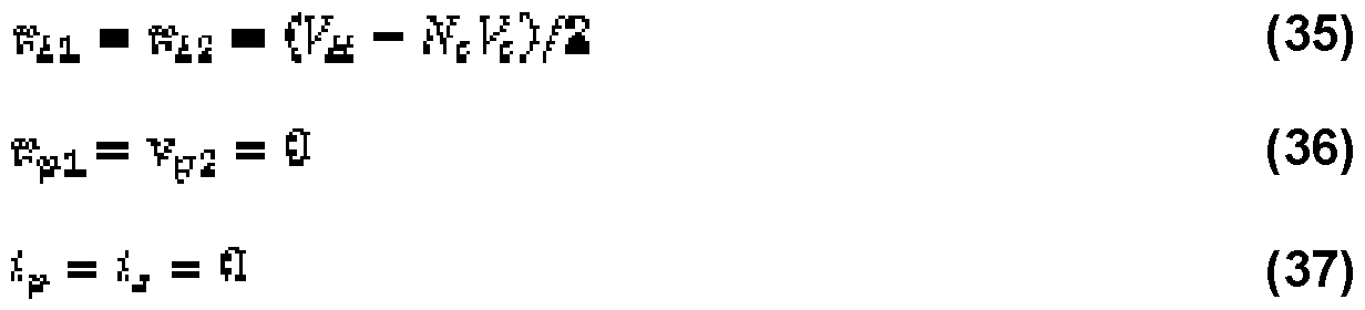
[00292] Therefore, through appropriate gating of St Ii and
 the average applied voltage to the transformer can be made to be equal to 0. This is to avoid saturation of the transformer. Additionally, the primary side transformer winding current is positive and equal to iL 1 when St_, is on and St l is off and negative and equal to -iL when S ll is off and ¾ is on. Therefore, the average dc current of the transformer can be minimized by reducing the difference between In anti f^, for instance.
[00293] An example of gating signals is provided in FIG. 51e, FIG. 51f and FIG.
51 g. Note, FIG. 51 corresponds to an alternate embodiment and this gating signal may not
work for a preferred embodiment described in this section. This alternate embodiment is referenced here strictly to illustrate what a gating signal pulse may look like.
[00294] When the gating signal is equal to a high value (in this particular example, the high value equals 1) the switch corresponding to this gating signal is triggered on. Conversely when the gating signal is equal to a low value (in this particular example, the low value equals 0) the switch corresponding to this gating signal is triggered off. Note, the gating signal values may be of different values other than 1. Additionally, the waveforms for the gating signals are idealized in FIG. 51. Furthermore, this is only one such example of a gating signal pulse, other types of gating signals are also possible.
[00295] Gating signals can be controlled through a controller device, which may reside on a same circuit, in some embodiments, or be interfaced with from another circuit (e.g., through an electronic interconnection). Gating signals may be associated with one or more clock signals which are used to synchronize the gating commands provided to various switches (e.g., the high / low values to be sent, or other values sent to the switches to operate them). Gating signals control timing of switch activation / actuation. The gating signals can be obtained, for example, as provided by a gating protocol stored thereon on machine-interpretable memory or instruction sets, which may be interpreted and executed on a processor or waveform function generator.
Discharge Mode
[00296] The three operating states for discharge mode are presented in FIG. 22. A similar analysis to that performed for the charge mode can be carried out for the discharge mode operating mode.
Reverse Power Transfer Mode
[00297] A similar analysis to that for forward power transfer mode can be carried out for the reverse power transfer mode operating modes. The 6 operating states for reverse power transfer mode are presented in FIG. 23 and FIG. 24. The analysis for reverse power transfer mode is similar to that of the forward power transfer mode case. However, an important difference between forward and reverse power transfer mode should be highlighted. The previous discussion on the forward power transfer mode considered passively controlled secondary side switches
 Unlike, for the forward power transfer mode case, in the reverse power case, active control of the secondary side
switches is required in some embodiments. In the reverse power transfer mode case, the gating of the isolation stage primary side switches
Unlike, for the forward power transfer mode case, in the reverse power case, active control of the secondary side
switches is required in some embodiments. In the reverse power transfer mode case, the gating of the isolation stage primary side switches
 is synchronized with the gating of the isolation stage secondary side switches

[00298] In some embodiments, the gating
 and S„, i is complementary to the gating of ¾ and
 As way of illustration, when St j = 1 and ¾ = 0: if ¾a
 are on and ¾ and Sn U are off, power will be delivered by the lower-voltage network. Conversely, and ¾ are off and
 are on power will be delivered to the lower-voltage network. When
 are off and ^ and ¾a are on power will be delivered by the lower-voltage network. Conversely, if
 and ¾ are on and ¾ are off power will be delivered to the lower-voltage network. Therefore in the reverse power case,
 are gated on and ¾ and
 are gated off for intervals when St U = 1 and ¾ = 0; and SViii and
 are gated off and ,3^^ and S„Il are gated on for intervals when SC U = 0 and ¾ = 1. This can be observed in FIG. 23 and FIG. 24.
Alternate Embodiment #2
[00299] In this section, the operating principles specific to the alternate embodiment of FIG. 5 are described. Please refer to FIG. 25 to FIG. 28 for the operating states specific to this embodiment. Note, unlike in a preferred embodiment of FIG. 3, ¾ > 0 is both forward and reverse power transfer mode in this alternate embodiment.
Forward Power Transfer Mode
[00300] There are 6 main operating states during forward transfer mode: 3 operating states during charge mode and 3 operating states during discharge mode.
These 6 operating states are described further in this section.
Charge Mode
[00301] The 3 main operating states during charge mode are described in FIG. 25. The three operating states are defined by the states of
 and¾.
and¾.
[00302] FIG. 25a corresponds to the condition where St is on and ¾ is off. Key voltages and current relations for this operating state are described by the following equations,

[00303] Where, n» is the turns ratio of primary winding 1 with respect to the secondary winding of the transformer; and ntå is the turns ratio of primary winding 2 with respect to the secondary winding of the transformer.
[00304] FIG. 25b corresponds to the condition where St Si is off and St i is on. Key voltages and current relations for this operating state are described by the following equations,


[00305] FIG. 25c corresponds to the condition where both St li and ¾ are on. The main voltages and currents impressed in this operating state are described by the following equations,
¾i - t¾ - ¾¾) (54)
¾3 = o (55) i= 0 (56)

¾ = 0 (58) fa hi (59) h = fl (60)
[00306] Therefore, similar to the embodiment of FIG. 4, through appropriate gating of St U and St ·, the average applied voltage to the transformer can be made to be equal to
0. This to avoid saturating the transformer. The primary side transformer winding 1 current is negative and equal
 is when SC U on and ¾ is off. The primary side transformer winding 2 current is positive and equal to
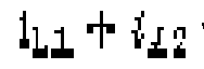 when SC U is off and
 is on.
[00307] Therefore, the average current of the transformer can be made to be equal to 0 through appropriate control action of
 Unlike in the alternate embodiment of FIG. 4, in this embodiment minimizing the difference between the inductor currents, hi- hi, is not necessary for minimizing the average dc current through the transformer windings. This is because the currents conducted by the primary side of the transformer are equal to the sum of the inductor 1 and inductor 2 currents in this embodiment.
Discharge Mode
Unlike in the alternate embodiment of FIG. 4, in this embodiment minimizing the difference between the inductor currents, hi- hi, is not necessary for minimizing the average dc current through the transformer windings. This is because the currents conducted by the primary side of the transformer are equal to the sum of the inductor 1 and inductor 2 currents in this embodiment.
Discharge Mode
[00308] The three operating states for discharge mode are presented in FIG. 26. A similar analysis to that performed for the charge mode can be carried out for the discharge mode operating mode. Therefore, the discharge mode is not discussed further here.
Reverse Power Transfer Mode
[00309] A similar analysis to that for forward power transfer can be carried out for the reverse power transfer mode operating modes. The 6 main operating states for reverse power transfer mode are presented in FIG. 27 and FIG. 28. The analysis is not detailed here.
The reverse power transfer mode cases are similar for the alternate embodiment of FIG. 4 and therefore is not discussed further here.
Control Considerations
[00310] In this section, an analysis is performed to demonstrate one possible control approach for a preferred embodiment. A similar control approach can be employed for the two alternate embodiments with the isolation stage. Note there are multiple ways to realize the control of this converter this is only one such implementation. The control objectives for this control approach are as follows:
1. Regulate the lower voltage network voltage, V0, to a reference value.
2. Minimize the difference between the two CSM inductor currents, ILI-IL2 = 0.
3. Regulate the sum of the VSM sub-module voltages, t¾a to a reference value. Note, the sum of the VSM sub-module values can be calculated via the following expression,

4. Regulate the individual voltage sub-module voltages.
[00311] This section describes this control approach with respect to the forward power transfer operation case. However, this control approach can be similarly applied to
the reverse power transfer operation case with some modifications which are detailed in the section following this one.
[00312] One or multiple controller devices take measurements of the circuit states such as current and voltage. This may be done by current measurement devices and voltage measurement devices, respectively, for example.
[00313] These measurements are fed as input signals to the controller devices. These input signals are then processed by the one or multiple controller devices. The one or multiple controller devices generates output signals.
[00314] These output signals in a preferred embodiment are influenced by the measurement inputs. However, this may not be the case in some embodiments. The gating signals fed as an input to the directly controllable switches of the converter may originate from the one or multiple controller devices, in some embodiments. Examples of the controller device includes a microcontroller or FPGA.
[00315] The control approach or control algorithm is stored in memory on the one or multiple controller devices in some embodiments. In a preferred embodiment the control approach or control algorithm influences how the input signals are processed by the one or multiple controller devices which in turn influences the gating signals.
Steady-State Analysis
[00316] If volt-second balance is applied to the two inductors and l_2 for a preferred embodiment over a switching period, the following two expressions can be derived,

[00317] where, D0 X [0.1] is a duty ratio term which denotes the relative duration of the charge and discharge operating modes;
 denotes the average over a switching period.
[00318] Since, «ί
 in steady-state, the above equations can be re-arranged to solve for the following expressions for Nc and Nd,

[00319] Since, D0 is unknown, an additional expression must be derived.
[00320] By employing Eq. 2 and Eq. 6, the average power delivered to the VSM string over a switching period can be expressed as follows,

[00321] where, the first term denotes the average power delivered to the VSM string during charge mode; the second term denotes the average power delivered by the VSM string during discharge mode.
[00322] This expression for ?e ¾ can be simplified by noting that in steady-state
 0 and in addition in steady-state if the control objectives are met the output current, l0, is equally shared between iu and h, i.e.

[00323] Therefore, the expression (63) for following expression,

[00324] The above expression can be re-arranged and simplified into the following,
£],¾ = ¾S‘ (66)
[00325] Expressions for Nc and Nd were previously derived in (62). By substituting these two expressions into (66) and then simplifying, the following expression for D0 can be derived,
 [00326] Therefore in this particular implementation of the control, the outer duty ratio, Do, is a function of the lower-voltage network voltage, V0, and the higher-voltage network voltage, VH.
[00327] This expression for D0 can be substituted into (62) resulting in the following expressions for Nc and Nd,
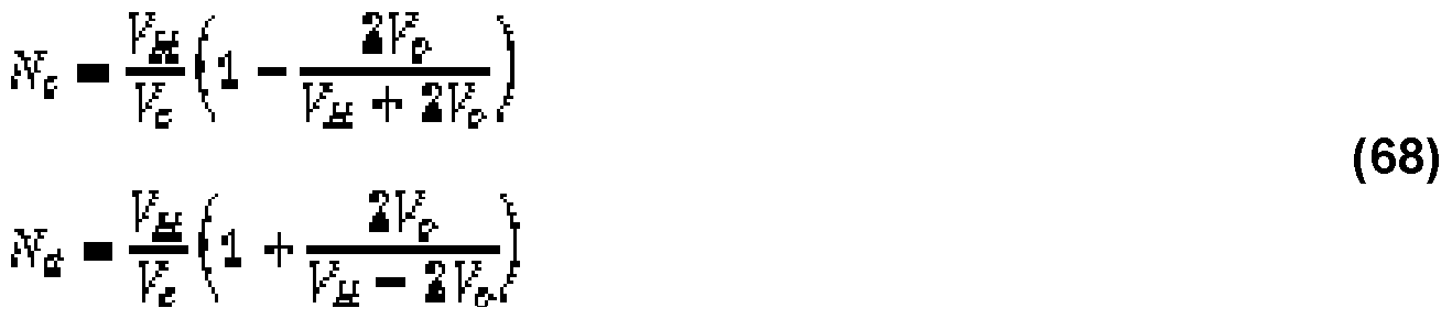
[00328] Note, Nc and Nd are continuous numbers and denote the average number of cells inserted during the charge and discharge intervals. However, it is important to note that due to the modular nature of the VSM string vs(t) can only take on fixed voltage levels.
[00329] Therefore, the control functionality of the converter controller is such that the average number of cells inserted during charge mode equals Nc and the average number of cells inserted during discharge mode equals Nd.
[00330] This can be expressed as follows,
¾ = åU¾J+ wtl
(69)

[00331] Where Dd e [o,'_] is a duty ratio term specific to the VSM charge operating mode; Dd£ [¾1] is a duty ratio term specific to the VSM discharge operating mode;
[ lrepresents the ceiling function; [] represents the floor function.
[00332] Charge mode consists of two sub-intervals in this particular control implementation. In sub-interval 1 , [¾ VSMs are inserted and in sub-interval 2 |¾1 VSMs are inserted. [tYsJ and [fYsl are separated by 1 VSM cell in this control implementation.
Therefore, [fYcl- [iYj = 1; Dc denotes the relative duration of GϊUE1 with respect to L¾J during charge mode. The discussion, for the Nd terms follows similarly and therefore is not discussed here.
If the expressions of [¾] = [i \ -b and ¾1■ L¾J + 1 are substituted into (69) the resulting expressions for Dc and Dd can be derived, flB - l - ¾ + UV
(70) Btf - ¾ - L¾J
[00333] Therefore, by selecting Dc and Dd as per the above expressions, the continuous Nc and Nd values are obtained even though the VSM string vs(t) features only fixed voltage levels.
[00334] It should be noted that in this analysis it is assumed that in both charge and discharge mode the average Nc and Nd values are controlled through the adjustment of the relative dwell times of two adjacent voltage levels G » ( [iVcJ and H^l for instance) of vs(t), respectively. However, this is only one such approach. For instance, it is possible to obtain the average Nc and Nd values by adjusting the relative dwell times of voltage levels that are not adjacent. Additionally, it is possible to use more than 2 sub-intervals during charge and discharge mode, for instance.
[00335] Therefore from the above control approach there are in effect 4 sub intervals for the converter with the implemented control. The charge mode consists of 2 sub-intervals and the discharge mode consists of 2 sub-intervals. A summary of the 4 sub intervals is provided here.
Charge Mode:
[00336] In sub-interval 1 , sub-modules are inserted in the

circuit for a duration equal to £3P£3ff^
[00337] In sub-interval 2, + Ί sub-modules are inserted in the circuit for a duration equal to
Discharge Mode:
[00338] In sub-interval 3, iYa = sub-modules are inserted in the circuit for a duration equal to ΰ?ΰa
[00339] In sub-interval 4,
 = i — 1 sub-modules are inserted in the circuit for a duration equal t

Regulation of the Individual Cell Voltages
[00340] The approach presented in the previous section will ensure that the total sum of the VSM cell voltages is regulated. However, additional control functionality is required in some embodiments to control the individual VSM voltages of the VSM strings. To control the individual VSM voltages, a sort and select control approach is employed in a preferred embodiment to the invention.
[00341] Over a given switching period, some VSM cells will be receive an excess of charge while some VSM cells will receive a deficit of charge in the control approach proposed in the preceding section.
[00342] In order to regulate the voltage of the individual VSM cells, in this sort and select control approach, gating signals are distributed to the VSM cells such that the cells of lowest state of charge receive an excess of charge; while the VSM cells of greatest state of charge receive a deficit of charge over the given switching periods. Note, this is only one such implementation for controlling the individual cell voltages. Other approaches are also possible.
Reverse Power Transfer Mode
[00343] To reverse the power direction from the lower-voltage network to the higher- voltage network, the CSM switch GMia is off and
 is on when pt fl; and SMlit is on and
SlS i is off when
 ^ fl. The gating of Se3 lt and SC3 i is synchronized with the charge and discharge operating modes of the converter in order to realize this reversal of power from the lower-voltage network to the higher-voltage network..
[00344] Note, the gating of . CJ^ and
 for reverse power transfer mode is made just prior to the polarity reversals of vt in some embodiments. This is required to turn-on switching devices in some embodiments that requires a positive voltage to turn-on.
Summary
for reverse power transfer mode is made just prior to the polarity reversals of vt in some embodiments. This is required to turn-on switching devices in some embodiments that requires a positive voltage to turn-on.
Summary
[00345] In summary, through adjustment of the duty cycles D0, Dc and Dd together with the appropriate selection of the number of sub-modules Nc, and Nd corresponding to the 4 sub-intervals, the control objectives of this particular application of the control can be achieved in steady-state. Note, this is only one such control implementations. Other control objectives and control approaches are also possible for this invention
Additional Details
[00346] In this section, some additional aspects of some embodiments of the topology are described.
[00347] By separating the power inductor from the HV loop by the CSM, the topology features both a fast di/dt during commutation intervals (limited by the HV loop inductance) and also a slow di/dt limited by a CSM inductor inductance. This combination of both a slow and fast di/dt enables a VSM string current, iH, that both features fast direction changes but also a controlled magnitude with low ripple component in some embodiments. The CSM in effect clamps the string current when undergoing a direction change.
[00348] Short commutation intervals enable the converter to realize greater effective switching frequencies. Higher effective switching frequencies enable reduced capacitance for the capacitors and inductances for the inductors in the circuit, for instance. An example of a higher effective switching frequency may be 10 kHz in some embodiments of the invention. The conventional ac transformer operates at line frequency which is at 50 or 60 Hz and therefore with this topology it is possible to operate at higher frequencies than ac grid connected systems. In some embodiments with the isolation stage, the ac frequencies seen by the isolation stage transformer are not restricted to being at the line frequency as in conventional ac distribution grid transformers. Therefore, the transformer can potentially made much cheaper and with less volume in these embodiments compared to a transformer for ac grid applications. Additionally, by operating at the higher effective switching frequencies it enables reduced capacitances of capacitors and inductances of inductors in some embodiments of the invention.
[00349] The slow di/dt of the CSM inductor inductance enables a dc-current to be delivered to the lower-voltage dc network with small ripple. An advantage of this is that the peak currents through the circuit are reduced and in addition the lower-voltage network
capacitance sinks the ripple current of the CSM inductor or inductors in some
embodiments.
[00350] Therefore, if larger ripple currents were delivered to the lower-voltage dc network capacitor the lower-voltage dc network capacitor may have to be increased compared to the case for low ripple currents.
[00351] In some embodiments, power is exchanged bi-directionally between the VSM string and the higher-voltage dc network in-order to ensure VSM string energy balance. When the HV-side current, IH, is of positive current direction, power is delivered from the higher-voltage dc network to the VSM string and to the CSM. When the HV-side current, IH, is of negative current direction, the VSM string delivers power to the higher- voltage dc network and to the CSM. Therefore, through the application of a sufficiently long negative current interval, voltage regulation of the VSM string is achieved.
[00352] In some embodiments, mixed frequency ac and dc voltage components are generated within the converter in order to balance the VSM string and to deliver power to the CSM. This enables a dc current component to flow through the VSM string while still maintaining energy balance of the VSM string. The ac components can be of a higher frequency as the HV loop inductance can be made sufficiently small. Furthermore, this topology enables a VSM string current of near-square wave waveshape to propagate down the VSM string. This combination of higher frequency ac components and a near square wave current waveshape enables reductions to the converter inductances and capacitances.
[00353] In some embodiments, it is the CSM that shapes the VSM string current. By using the CSM to shape the current, the current direction can be quickly changed and the magnitude controlled.
[00354] The CSM shapes the string current as it is in series with the string. In a preferred embodiment, with a set of CSM switch states the string current is equal to an inductor current. Similarly, with another set of CSM switch states, the string current is equal to the negative of an inductor current. By controlling (either directly or indirectly) these CSM switch states, then the string current can be made to be equal to the inductor current and equal to the negative of an inductor current over a switching period.
[00355] It is in this way that it is said that the CSM shapes the string current. Since the string current amplitude during these two cases is equal to a CSM inductor current and is equal to either a positive or negative of this inductor current depending on the state of the CSM switches.
[00356] The string current can be quickly reversed as there is no required external inductor in series with the VSM string in some embodiments.
[00357] After the control acts to change the direction of the current into the series string a commutation or free-wheeling state first occurs where a loop is formed wherein the current in the series connected string is equal to a loop current and accordingly, there is no inductor of the CSM limiting a change in the current into the series connected string and an inductance in the loop is only a leakage inductance of the loop. It is also possible to add an external leakage inductance and actually this may be preferable in some embodiments.
[00358] Therefore the only inductance in this loop is the leakage inductance of the loop in some embodiments. Because the leakage inductance is typically of relatively small value, a fast change in string current di/dt can be realized.
[00359] Note, it is also possible to insert an external inductor alternatively termed a choke in series with the series string. Note, series string is the same as string of sub- module elements. The addition of this external inductor is shown in FIG. 30. If this external inductor is added in series with the string then during commutation or freewheeling states, this external inductor will always be in the circuit with the string and therefore will limit the rate of change in the string current value.
[00360] The inductance within the CSM ensures the current at the CSM DC side terminals remains nearly constant throughout switching of the CSM switching elements. The CSM switching elements are operated to route this current either up the high voltage string towards the positive high voltage DC terminal or towards the negative high voltage DC terminal. The CSM switches can also circulate the low voltage side current by imposing a short-circuit current path.
[00361] Regarding the optional galvanic isolation stage. At across the input terminals of the CSM, there exists in some embodiments both dc and ac voltage components. Furthermore, the VSM string current features both dc and ac current components in some embodiments. The structure of the CSM together with the optional
galvanic isolation stage enables the converter to feature galvanic isolation without saturating the transformer nor circulating dc-current within the transformer.
Rating of Converter Elements
[00362] This section provides equations that could be used for guidance in rating the converter elements of the converter. Note, these are simplified equations and therefore other approaches could also be employed. This is only one such approach.
VSM String
[00363] The minimum number voltage sub-modules required,
approximated by eq. (71),

[00364] In practice, additional sub-modules may be required for redundancy reasons.
[00365] The maximum current conducted by the VSM cells can be approximated as follows, eifrme* = hΐek ΐi,ίί;) (72)
[00366] The average current conducted by the inserted VSM cells during charge mode can be approximated as follows, l t l EJ ifr = ii l (73)
[00367] The average current conducted by the inserted VSM cells during discharge mode can be approximated as follows, EΪRIPB, — iis (74)
Current-Source Module Element
[00368] The maximum voltage magnitude across the terminals of the CSM can be approximated as follows,
 Other Design Considerations
DC-Side Filtering
A dc-side filter can be added between the series string of VSMs and the CSM and the high-voltage dc network as shown in the alternate embodiment of FIG. 29. This is a preferred embodiment of the dc-side filter however other configurations of the dc-side filter are also possible. Some of the advantages of a dc-side filter include:
1. Reducing the commutation loop inductance when reversing the direction of the HV loop current, IH;
2. Filtering of harmonics generated by the converter; and
3. The ability to use an inductor in series with the higher-voltage network to reduce fault currents without increasing the commutation loop inductance.
DC-Side Choke
[00369] A choke inductor can be added in series with the topology as shown in the alternate embodiment of FIG. 30. A choke inductor decreases the di/dt in the HV loop which can be advantageous.
[00370] As an example, in some embodiments if at least one of the voltage levels of vs (refer to FIG. 3 for reference to vs) is sufficiently close to VH (for example, if vs (t)=VH (t)) it is possible for the HV and LV loops to become decoupled during the interval where vs is sufficiently close to VH.
[00371] This interval could be in either the charge and/or discharge operating modes. When the HV and LV loops become decoupled under this condition, it is desirable in some embodiments that the magnitude of IH not deviate significantly from
[00372] Since, the change in IH when the HV and LV loops are decoupled is influenced by the HV loop inductance, by selecting a choke of sufficiently high inductance it is possible to reduce the di/dt of the current during this condition. This enables a more near square wave waveshape for the HV loop current iH to be realized.
[00373] Therefore, in some embodiments it may be desirable to include a choke inductor in the HV loop electrically in series between the higher-voltage dc network and the string of sub-module elements as shown in the alternate embodiment of FIG. 30.
[00374] Note in FIG. 30, the higher-voltage dc network is represented for illustrative purposes as a dc voltage source; however, this is only one such representation.
[00375] For instance, it may be desired to include an input filter between the choke inductor and the higher-voltage dc network. In this instance, the higher-voltage dc network could be considered as a dc voltage source with an input filter for example. Referring to FIG. 29, if an input filter is considered, the choke inductor would be electrically connected in series between the string of voltage and current source sub-module elements and the input filter. This can also be visualized from FIG. 30 if the higher-voltage dc network is instead represented as a dc-voltage source with an input filter.
[00376] Note, the larger the series inductance, the longer the commutation intervals will be assuming all else is maintained the same. Therefore, by introducing a dc-side choke the maximum effective switching frequency of the converter may be constrained.
Simulation Results
[00377] To demonstrate the operation of the converter, 7 simulation cases are provided. The simulation case results are provided in FIG. 31 to 37. These cases demonstrate steady-state and transient operation in forward power transfer mode as well as steady-state operation in reverse power transfer mode.
[00378] The simulation cases 1 to 3 are for a preferred embodiment of FIG. 3. The simulation cases 4 to 5 are for the alternate embodiment of FIG. 4. The simulation cases 6 to 7 are for the alternate embodiment of FIG. 5. The main circuit parameters for these simulation cases are provided in Table 1 and Table 2.
Table 1 - Common Parameters


Table 2 - Case Specific Parameters

Case 1 : Steady-State Forward Power Operation for FIG. 3 Topology
[00379] FIG. 31 presents operating waveforms for the steady-state forward power transfer case. These simulation results are for a preferred embodiment of FIG. 3.
[00380] In this case, the high-voltage dc network supplies 7.6 kW of power to the 380 V lower-voltage dc network. From the simulation results, it is shown that the average energy in the VSM string is approximately 69 J. This is consistent with the average cell voltages being maintained at the nominal voltage of 400 V as can be verified by the following equation,

[00381] This simulation case shows that the lower-voltage network voltage is regulated to the desired reference voltage of 380 V.
[00382] It is also important to highlight that the HV loop current, iH, is of nearly square-wave shape and the converter is operating at an effective switching frequency 10 kHz. Additionally, the average current inductor U and l_2 currents, lLi and lL2, are approximately equal to lo/2=10 Amp. The average HV loop current, iH, during charge mode is equal to IL1 and equal to -lL2 during discharge mode.
Case 2: Steady-State Reverse Power Operation for FIG. 3 Topology
[00383] FIG. 32 presents the results for Case 2 which is the reverse power transfer mode case. These simulation results are for a preferred embodiment of FIG. 3. In this case, the lower-voltage network delivers 7.6 kW of power to the 3 kV high-voltage dc network.
[00384] This reversal of power flow can be directly seen as v0 and i0 are of opposite polarity, for instance. Additionally, the HV loop current, in is out of phase with respect to the voltage across the input terminals of the CSM, vt. The simulation results show that the energy in the upper VSM string = 68.4 J which demonstrates that energy balance in the VSM string is achieved.
Case 3: Transient Forward Power Operation for FIG. 3 Topology
[00385] FIG. 33 presents the results for Case 3 which is a transient case for the forward power transfer mode. These simulation results are for a preferred embodiment of
FIG. 3.
[00386] In this case, the higher-voltage dc network is initially supplying 3.8 kW to the low-voltage dc network. At t = 0.51s, the load undergoes a step change from 3.8 kW to 7.6 kW. It takes approximately 300 ms for the system to stabilize. At t = 0.54s, the load undergoes a step change from 7.6 kW to 1.9 kW. It takes approximately 200 ms for the system to stabilize. The ripple voltage in the VSM cell capacitors can be observed as being
dependent on the output load current. It is also shown that the average energy in the VSM string is maintained at approximately 69 J throughout the step changes and therefore energy balance in the VSM strings is maintained. Additionally, the step-changes in load are accompanied by temporary deviations in the lower-voltage dc network voltage as is expected.
Case 4: Steady-State Forward Power Operation for FIG. 4 Topology
[00387] FIG. 34 presents operating waveforms for the steady-state forward power transfer case. These simulation results are for the alternate embodiment of FIG. 4.
[00388] As can be observed 7.6 kW of power is transferred to the lower-voltage dc network. The VSM string energy is balanced over a switching period. The inductor and l_2 are shown to share the lower-voltage network current.
[00389] Additionally, the secondary side voltage of the transformer vs can be observed to be ½ the primary side voltage, corresponding to a 2:1 turns ratio for the transformer. The applied voltage to the transformer windings appears to be ac with a near square-wave waveshape. Additionally, the primary and secondary side currents of the transformer appear appears to be ac with a near square-wave waveshape.
Case 5: Steady-State Reverse Power Operation for FIG. 4 Topology
[00390] FIG. 35 presents operating waveforms for the steady-state reverse power transfer case. These simulation results are for the alternate embodiment of FIG. 4.
[00391] As can be observed 9.175 kW of power is delivered by the 367 V low- voltage dc network.
[00392] The VSM string energy is balanced over a switching period. The inductor and l_2 are shown to share the lower-voltage network current. Additionally, the secondary side voltage of the transformer vs can be observed to be ½ the primary side voltage, corresponding to a 2:1 turns ratio for the transformer. The applied voltage to the transformer windings appears to be ac with a near square-wave shape. Additionally, the primary and secondary side currents of the transformer appear to be ac with a near square-wave shape.
Case 6: Steady-State Forward Power Operation for FIG. 5 Topology
[00393] FIG. 36 presents operating waveforms for the steady-state forward power transfer case. These simulation results are for the alternate embodiment of FIG. 5.
[00394] As can be observed 9.5 kW of power is transferred to the lower-voltage dc network. The VSM string energy is shown to be balanced over a switching period. The inductor U and l_2 are shown to share the lower-voltage network current.
[00395] Additionally, the secondary side voltage of the transformer vs can be observed to be equal to the primary side voltage, corresponding to a 1 :1 turns ratio for the two primary windings of the transformer with respect to the secondary winding.
[00396] The applied voltage to the transformer windings appears to be ac in nature with a near square-wave waveshape. Additionally, the primary and secondary side currents of the transformer appear to be ac in nature with a near square-wave waveshape.
Case 7: Steady-State Reverse Power Operation for FIG. 5 Topology
[00397] FIG. 37 presents operating waveforms for the steady-state reverse power transfer case. These simulation results are for the alternate embodiment of FIG. 5.
[00398] As can be observed 8.65 kW of power is delivered from the lower-voltage dc network to the higher-voltage dc network. The VSM string energy is shown to be balanced over this interval. The inductor and l_2 are shown to share the lower-voltage network current.
[00399] Additionally, the secondary side voltage of the transformer vs can be observed to be equal to the primary side voltage, corresponding to a 1 :1 turns ratio for the two primary windings of the transformer with respect to the secondary side of the transformer. The applied voltage to the transformer windings appears to be ac in nature with a near square-wave waveshape. Additionally, the primary and secondary side currents of the transformer appear to be ac in nature with a near square-wave waveshape.
Alternate Embodiment
[00400] An alternate embodiment is presented in FIG. 38. A preferred embodiment of the voltage source sub-module for this alternate embodiment is presented in FIG. 39. A preferred embodiment of the current source sub-module for this alternate embodiment is presented in FIG. 40 for uni-directional and bi-directional power transfer, respectively. An example implementation of the alternate embodiment is presented in FIG. 41.
Approaches may be provided in various combinations and are not limited to the specific embodiments described. For example, different method step order, orientations, and alternatives are contemplated in addition to the alternate embodiments.
[00401] In the example implementation, there are three voltage-source sub-modules and three current-source sub-modules, however the number of voltage sub-modules and current-sub modules is scalable as noted in FIG. 38.
[00402] In the following section the elements of various alternate embodiments are described.
[00403] This is followed in a later section by a description of the operating modes, control as well more detailed design considerations.
[00404] Various equations are provided in the sections below. It is important to recognize that the equations are provided as instructive examples, other approaches are possible. For example, some examples are more qualitative then quantitative, from an example perspective.
[00405] They are used to illustrate in a very idealized way the approximate ratings of various topologies. In practice, the determination of the minimum number of VSM cells, for instance, may be quite different. There are other approaches possible, especially in view of practical considerations (e.g., adjustments may need to be made in view of real- world adjustments, such as for environmental factors, parasitics, non-idealities, among others).
[00406] Regarding notation for this alternate embodiment:
• The lower-voltage dc RMS voltage is the same as the average lower-voltage dc network voltage
The main loop current, idC, is the same as the higher-voltage loop current
Description of the Voltage Source and Current Source Element Blocks Series String of Sub-Modules of Voltage-Source Type
[00407] As shown in FIG. 39, the VSM string includes a series connection of multiple voltage source sub-modules. An example implementation of the VSM string is presented in FIG. 42. In the alternate embodiment, the sub-modules are of a half-bridge type consisting of two series switches and a capacitor across the outer terminals of the two switches.
[00408] Additionally, in the alternate embodiment, the sub-modules are combined into a single stack. With half-bridge type sub-modules, a maximum uni-polar voltage can be created by the VSM string, equal to the following:

[00410] Where, N is the number of voltage sub-modules;
 is the voltage of sub- module capacitor i; and
 is the sum of all sub-module capacitor voltages.
[00411] Referring to FIG. 38, the VSM string is electrically connected such that the positive polarity end of the stack is electrically connected to the positive terminal of the higher-voltage side network and the negative terminal to the positive rail of the LV bus.
[00412] With this electrical connection, the voltage imposed by the VSM string opposes the voltage of the higher-voltage network allowing for a lower voltage to be controlled for across the terminals of the current source modules. In this disclosure, the sub-module at the positive polarity end of the stack is called the upper sub-module; and the sub-module at the negative polarity end of the stack is called the lower sub-module. Modules are implemented as electronic circuits and may contain one or more electrical components.
[00413] In an alternate embodiment, it is important to highlight that the stack can be equivalently re-located such that the positive terminal of the stack is electrically connected to the negative terminal of the lower-voltage bus and the negative terminal of the stack is electrically connected to the negative terminal of the higher-voltage dc network. In another
further embodiment, it is also equivalent to distribute the sub-modules into multiple stacks. These stacks can be electrically on either side of the lower-voltage bus.
[00414] In the alternate embodiment, the mid-point of the upper most sub-module (sub-module 1 in FIG. 39) is electrically connected to the positive polarity terminal of the higher-voltage network. For all other sub-modules, the mid-point of the two series switches is electrically connected to the negative terminal of the capacitor above it.
[00415] For instance, referring to FIG. 39, the mid-point of sub-module 2 is electrically connected to the negative terminal of the capacitor of sub-module 1. The negative terminal of the lower sub-module is electrically interfaced to the positive rail of the LV bus.
[00416] The minimum requirements of the switches of each sub-module are uni polar voltage blocking capability and bi-directional current conduction capability. Switches that meet this criteria are MOSFETs and IGBTs with anti-parallel diodes, for instance.
[00417] One possible approach for calculating the minimum number voltage sub- modules required, ¾¾, is presented in eq. 78,


[00420] For instance, if the lower-voltage network voltage was selected to be 500 V and the sub-module voltages are at 400 V, the maximum voltage across the lower-voltage bus terminals, in one possible implementation of the control could be, 400 V * 2 = 800 V. It is also possible to employ different modulation strategies involving less or additional cells, depending on the lower-voltage network voltage, which would impose lower or higher maximum lower-voltage side bus voltages, respectively.
[00421] In practice, additional sub-modules would be required for redundancy reasons.
[00422] One possible approach for calculating the minimum blocking voltage requirements of the VSM stack is presented in eq. 3,

[00424] In an alternate embodiment, all sub-modules are identical. However, it is also possible to use different voltage sub-module types in the string, in an alternate embodiment. For instance, a mixture of half-bridge and full-bridge sub-module types could be employed, for instance. In addition, a string of only full-bridge sub-module types could also be employed, for instance. The sub-modules can also have different nominal voltage values as well as states-of-charge.
[00425] It is also important to note that it is possible to also parallel multiple voltage source sub-module elements. By paralleling the voltage source sub-module elements, the loop current is shared between the paralleled elements. If paralleling voltage sub-module strings, a di/dt reactor can be employed between the VSM strings to limit the di/dt due to voltage imbalances in the strings, for instance.
Current-Source Type Sub-Modules
[00426] An alternate embodiment of the CSM is presented in FIG. 40. Depending on the type of switch utilized the CSM can feature either uni-directional or bi-directional power transfer capability.
[00427] The CSM has two ac side terminals and two dc side terminals in some embodiments. The ac terminals are not electrically bonded to either of the two dc terminals of the CSM in some embodiments. The ac terminals are connected in series with the VSMs. The dc terminals are connected to the lower-voltage dc network.
[00428] An example implementation of a CSM with uni-directional power capability is presented in FIG. 43 and with bi-directional power capability in FIG. 44. In the alternate embodiment, each current source sub-module consists of a single-phase current source converter front-end with an inductor. For uni-directional power capability, the minimum
requirements for the switches of the front-end include uni-polar voltage blocking capability and uni-direction current conduction capability.
[00429] An example switch implementation for uni-directional power capability are diodes. The CSM resembles in this embodiment
[00430] a full-bridge diode rectifier. For the bi-directional power capability, the minimum requirements for the switches of the front-end are bi-polar voltage blocking capability and uni-direction current conduction capability. An example switch
implementation for the front-end are GTOs or IGBTs with a series diode, for instance. The CSM resembles in this embodiment a single phase current source inverter (csi).
[00431] The CSM operates as a load, when for instance the higher-voltage dc network is supplying power to the lower voltage dc network connected across the output terminals of that CSM. Referring to FIG. 40, when the LV bus voltage, vt, is of positive polarity, a positive iAV implies power is being delivered to the CSM; and a negative
 implies power is being delivered by the CSM.
[00432] Furthermore, when the LV bus voltage, vt, is of negative polarity, a negative ie/i4 implies power is being delivered by the CSM; and a positive
 implies power is being delivered to the CSM. Uni-directional power transfer operation is demonstrated in FIG. 47. Bi-directional power transfer operation is demonstrated in FIG. 48. When the front-end switches are implemented by controllable devices, such as GTO or IGBT with a series diode, then an approach for achieving approximately constant power to the load would be to gate the Si and S4 front-end switches such that
 is positive when v¾ is positive; and gate the S2 and S3 switches such that iSiM is negative when ¾ is negative.
[00433] Similarly, an approach for achieving approximately constant power delivery by the load, for bi-directional CSMs, would be to gate the S2 and S3 front-end switches such that is negative when
 is positive; and gate the Si and S4 front-end switches such that is positive when vb is negative.
[00434] In the alternate embodiment, as shown in FIG. 40, the voltage at the terminals of the lower voltage network,
is positive; and gate the Si and S4 front-end switches such that is positive when vb is negative.
[00434] In the alternate embodiment, as shown in FIG. 40, the voltage at the terminals of the lower voltage network,
 will be of positive polarity when power is being delivered to the lower voltage network. Conversely, the polarity will be negative when power is being delivered by the lower voltage network. In the alternate embodiment, the lower voltage network is represented as a capacitor with a parallel current source.
[00435] The capacitor functions as a filter. However, it is possible to employ different types of filtering approaches. In addition, this is only one such representation of the lower voltage dc network. For instance, the lower voltage network could be
represented as a resistive load.
[00436] One equation for calculating the blocking voltage requirement of the switches in the front-end is the following,

[00438] Where, t jAtmisis the voltage across the VSM string when the minimum number of sub-modules switched in the circuit;
 is the voltage across the VSM string when the maximum number of sub-modules is switched in the circuit. Generally, it is expected that t^will be equivalent to either 1 or 2 sub-module voltages. Where,

 depend on factors including the control method employed. In one such control method, the
 terms can be approximated by the following expressions,

[00439] Where, Vc is the nominal VSM cell capacitor voltage.
[00440] Therefore, only a fraction of the higher-side voltage is applied across the terminals of the CSMs. In addition, only a fraction of the higher-side voltage is applied across the power inductor of the CSM.
[00441] As shown in FIG. 38, it is possible to connect multiple current source sub- modules across the terminals of the LV bus. FIG. 38, shows a total of M CSMs connected across the LV terminals. Furthermore, the current source modules can have different load currents. Additionally, some current source modules may be generating power while others are consuming power.
[00442] It is also important to note that the CSM can be scaled to higher voltages through approaches such as series connection of multiple switches, for instance, enabling this mechanism to interface to lower voltage networks at higher voltages, for instance.
Operating Principle
[00443] To demonstrate the energy transfer mechanism, it is illustrative to first consider a single resistive load.
[00444] Referring to FIG. 45, in operating mode 1 , the voltage across the resistor is controlled to be, f¾ = Viv. In this operating mode, the higher-voltage dc network delivers power to the inserted voltage sub-modules and to the lower-voltage load resistor, fl. In operating mode 2, the voltage across the resistor is controlled to be,
 ■ -¾ . In this operating mode, the current direction in the main loop is reversed and the voltage sub- modules are discharged into the higher-voltage dc network and to the load. In both operating modes the magnitude of the current is,
 fit. Therefore, in both operating modes the power delivered to the load,

[00445] In operating mode 1 , the total voltage of the voltage sub-module string is,
In operating mode 2, the total voltage of the voltage sub-module string is,
 As the loop current is the same in operating mode 1 and 2, i.e.
 the relative on-time for operating mode 1 and 2 is made asymmetrical so as to balance the energy in the voltage sub-module string over a switching period. The
following details a calculation for the duty ratio in-order to balance the energy in the VSM string over a switching period for the circuit described in FIG. 45,
the relative on-time for operating mode 1 and 2 is made asymmetrical so as to balance the energy in the voltage sub-module string over a switching period. The
following details a calculation for the duty ratio in-order to balance the energy in the VSM string over a switching period for the circuit described in FIG. 45,

[00447] In operating mode 1 , from t=t0 to DTS, the power to the VSM string is determined as follows,

[00449] In operating mode 2, from t=DTs to Ts, the power to the VSM string is determined as follows,

[00451] Substituting eqs. 6 and 7 into 5,

[00453] where, D is the duty ratio.
[00454] Re-arranging eq. 8 for the duty ratio, D, yields,
[00455]

[00456] It is by varying the duty ratio that the energy in the VSM string can be controlled while power is delivered to the load.
[00457] A more detailed model is presented in FIG. 46, where the resistor is replaced by with a single-phase diode bridge with a resistor. For this circuit, in operating mode 1 , is applied across the terminals of the diode bridge, forward biasing S± and
54. The load current circulates through the main loop such that the VSM string is charged
[00458] Conversely, in operating mode 2, -V^ is applied across the terminals of the diode bridge forward biasing S2 and S3. The load current circulates through the main loop in the opposite direction such that the VSM string is being discharged. By using a diode- bridge, the voltage across the load resistor is in the ideal case constant through operating modes 1 and 2.
[00459] Expanding on FIG. 46 is FIG. 47. In FIG. 47, an inductor and capacitor is added between the resistor and the diode-bridge front-end. The capacitor may be part of the lower voltage network as outlined in FIG. 38 and the inductor is part of the CSM. A few of the purposes of the inductor, include:
■ Maintain continuity of main loop current
■ Maintain continuity of power delivered to the load.
■ Reduction in current ripple of the load and main loop current
[00460] The above describes one such approach for operating the invention when power is being delivered from the higher-voltage dc network to the lower-voltage dc network. Other variations on this approach are possible. It is also possible for this scheme to be operated such the lower-voltage side supplies power to the higher-voltage side. This is done by implementation of switches with bipolar voltage blocking and uni-directional conduction current capability. The operating modes where power is being delivered from the lower voltage network to the higher-voltage dc network is illustrated in FIG. 48.
Control of Voltage-Source Sub-Modules
Control of Lower-Voltage Bus Voltage and Energy Management of VSM String
[00461] By varying the number of voltage sub-modules which are inserted in the circuit, the lower voltage bus voltage can be controlled.
[00462] To control for an average lower voltage dc network voltage, ¾, which is an integer multiple of the sub-module cell voltages an approach that could be employed is to have two modes of operation where different number of sub-modules are inserted, as follows:
[00463] Mode 1 : From

[00464] Mode 2: From

[00465] Where, ¾_ is the number of inserted voltage sub-modules in operating mode 1 ; Hj is the number of inserted voltage sub-modules in operating mode 2; and
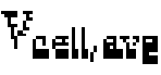 is the average voltage of a sub-module.
[00466] In mode 1 , a positive voltage is applied across the lower-voltage bus. In mode 2, a negative voltage is applied across the lower-voltage bus.
[00467] It is also possible to control for an average lower voltage dc network voltage which is a non-integer multiple of the sub-module cell voltages. An example of an approach that could be employed for this is to employ 2 modes of operation with 2 intervals each. Each mode and interval having a different number of inserted number of sub-modules, as follows:
[00468] Mode 1 , Interval 1 : From t = i-Q to ¾TS, ¾ '

[00469] Mode 1 , Interval 2: From

[00470] Mode 2, Interval 1 : From

[00471] Mode 2, Interval 2: From

[00472] By varying the relative dwell time of interval 1 and interval 2 in both modes 1 and 2 an average lower voltage dc network voltage which is a non-integer multiple of a sub-module voltage can be realized. In addition, by varying the duty ratio, D, the energy in the voltage sub-module string is controlled. A proxy for energy in the VSM string is the sum of all cell capacitor voltages in the VSM string. Therefore, another way to regulate the
energy in the string is to adjust D based on the sum of all cell capacitor voltages in the VSM string.
[00473] Note, these were examples of approaches that could be employed.
However, there are many alternate ways to control for a lower voltage dc network voltage. In addition, the sequence of these modes and intervals can be interchanged.
Energy Balancing Within Voltage Sub-Module String
[00474] As discussed in the preceding section, in order to control for the energy of the VSM string, the duty ratio between operating modes 1 and operating modes 2 can be adjusted. This enables control of energy to the VSM string; however, the individual voltage sub-modules within the string must also be balanced. This is best illustrated through an example for the case where the voltage across the lower-voltage bus is controlled to be a multiple of a cell voltage. As in the preceding section,
[00475] Mode 1 : From

[00476] Mode 2: From

[00477] Where,

[00478] In mode 1 , — ¾ VSMs are inserted. In mode 2, iY 4- ¾, VSMs are inserted. Therefore, if no VSM string energy balancing is performed, Y - ¾ VSMs will be maintained in the circuit for the entire switching period. While ΐ ¾ VSMs will be inserted in the circuit only during mode 2. This is only one such example scenario.
[00479] Therefore, if during a switching period, there is no energy accumulation in the VSM string, the
 cells will receive either an excess or deficit of energy depending on whether power is being delivered from the higher-voltage dc side network or whether power is being delivered from the lower-voltage dc network side. In case power is being delivered from the higher-voltage dc side network, iV - ¾ sub-modules will receive excess energy over a switching period and 2 ¾; sub-modules will receive a deficit of
energy over a switching period; conversely, if power is being delivered from the lower- voltage side, fV- ¾ sub-modules receive a deficit of energy over a switching period and
cells will receive either an excess or deficit of energy depending on whether power is being delivered from the higher-voltage dc side network or whether power is being delivered from the lower-voltage dc network side. In case power is being delivered from the higher-voltage dc side network, iV - ¾ sub-modules will receive excess energy over a switching period and 2 ¾; sub-modules will receive a deficit of
energy over a switching period; conversely, if power is being delivered from the lower- voltage side, fV- ¾ sub-modules receive a deficit of energy over a switching period and
2 ¾ receive an excess of energy over a switching period.
[00480] One approach for ensuring the individual sub-module energy remains balanced over a period of time is to ensure that the sub-modules that are receiving an excess of energy over a switching period are those sub-modules with the lowest state-of- charge and the sub-modules receiving a net deficit of energy over a switching period are those sub-modules at the greatest state of charge. It should be noted that there are multiple ways of implementing this sub-module balancing. Described is one such approach.
Control of Current-Source Module
[00481] For the uni-directional power capable CSM, with a diode front-end, the current source module is indirectly controlled. The states of the current source module diodes are indirectly set through the control of the VSM string. To this point, referring to FIG. 47, switches Si and S4 will be forward biased when VB is positive. S2 and S3 will be forward biased when vB is negative. The voltage vB is set by control of the VSM string. In steady-state and for the ideal case, the average value of the CSM inductor current will be equal to the average load current for the network interfaced to that CSM, lL, and the average value of the CSM terminal voltage, VLv, which is the lower voltage dc network voltage will be equal to the rms voltage of the lower voltage bus,

[00482] Referring to bi-directional operation, when power is being delivered from the lower voltage dc network, S2 and S3, are gated such that they are conduct the CSM current when vB is positive. Switches S2 and S3 can be gated when vB is negative. In steady-state, the average CSM inductor current will be equal to the average load current and the average value of the lower voltage network voltage of the CSM will be equal to the rms voltage of the lower-voltage bus.
Other Design Considerations
DC-Side Filtering
[00483] A dc-side filter capacitor can be added between the series string and the higher-voltage dc side as shown in FIG. 49. Please note that this is preferred embodiment for the dc-filter however other configurations of the dc-side filter are possible. This dc-side filter offers benefits such as the following:
■ By adding a dc-side capacitor across the input stage of the series string the series inductance seen by the converter during commutation intervals can be reduced. This reduction enables the converter to operate at higher switching frequencies while maintaining a near square-wave main loop current.
■ In normal steady-state operation, there is an ac current component being fed back to the higher-voltage dc-side. By adding a capacitive element, the ripple of the current through the higher-voltage dc side network can be reduced.
DC-Side Choke
[00484] A choke inductor can be added in series with the topology as shown in FIG. 50. A choke inductor limits the time rate of change of current in the main loop. The larger the series inductance, the larger the commutation interval will be when changing the direction of current in the main loop if all other circuit parameters are fixed.
Simulation Results
[00485] To demonstrate the operation of the scheme, four cases were simulated. The simulation case results are provided in FIG. 51 to 54. These cases demonstrate the CSM operating as a load, the CSM operating as a generator, multiple parallel CSMs, as well as a step change in load current. The circuit parameters for these cases are provided below in Table 3.
[00486] Table 3 - Circuit Parameters for Simulation Cases


[00487] FIG. 51 corresponds to Case 8, for which there is a single CSM. In this case, the higher-voltage dc side is supplying the power to the CSM. The load current is 20 Amp. The lower-voltage dc bus rms voltage = 500 V. From the simulation results, it is shown that the average energy in the VSM stack = approximately 2400 J. The energy of a voltage sub-modules can be estimated by eq. 10,
[00488] tf = - - (åfBl }“ m
[00489] Where,
 is the equivalent capacitance of the series string of VSMs; iV is the number of cells in the VSM stack; andE -1¾i\f,f is the total sum of the sub-module voltages in the string. From eq. 86, it can be determined that the total cell voltage under nominal operating conditions = 30*400 V which corresponds to 2400 J of energy storage. This implies that energy has been maintained across the VSM stack.
[00490] For Case 8, there are 5 unique gating signals for the voltage sub-modules of the string. These 5 gating signals are distributed to the appropriate voltage sub-modules in the string. A brief description of these 5 gating signals is provided here:
[00491] Of the cells, 23 of the 30 are continuously inserted in the circuit. This corresponds to a constant high gating signal.
[00492] Of the cells, 3 of the 30 are continuously by-passed. This corresponds to a constant low gating signal. The low gating signal is when we have redundant number of sub-modules. When there are no redundant sub-modules this low gating signal is not used.
[00493] Referring to FIG. 51, £0 denotes the start of a switching period. From t=fQ to 23 VSM cells are inserted in the circuit. From t=i1 to t2, 24 VSM cells are inserted in the
circuit. From t =t0 to t2 the voltage sub-modules of lowest state-of-charge have been inserted as during this interval the VSM string will be charged.
[00494] From t=t to t3, 26 VSM cells are inserted in the circuit. From t=t3 to
 27
27
VSM sub-modules are inserted in the circuit. From t=i2 to Ts, the voltage sub-modules of greatest state-of-charge have been inserted as during this interval the VSM string will be discharged.
[00495] It is important to note, that the individual VSM cells that are inserted during each of these four time intervals is expected to change during operation depending on such factors such as relative state-of-charge, for instance. For instance, in this simulation case study, there are 30 VSM cells. The 23 VSM cells that are continuously in the circuit for a given switching period could be any of the VSM cells 1 through to 30 as long as the total equals 23 cells. This logic applies to the other time intervals.
[00496] It is shown in this simulation case that the rms voltage of the lower voltage network is approximately equal to the rms voltage value of the input voltage at the lower- voltage bus, tv It is also important to note that the maximum voltage across the terminals of the CSM is approximately 800 Volts which is the equivalent voltage of 2 series voltage source modules.
[00497] Finally, it is important to highlight that the main loop current, idc, is of near- square-wave shape while the converter is operating at 1 kHz and a 500 rms voltage is applied across the lower-voltage bus terminals.
[00498] FIG. 52 presents the results for Case 9 which features a single CSM operating as a load where the power is being delivered by the higher-voltage dc side. The load current is initially 10 Amp. At t = 1s, the load changes from 10 Amp to 20 Amp. It takes approximately 200 ms for the system to regain steady-state.
[00499] In this case, it is shown that the average energy in the VSM string = 2400 J, implying that energy balance in the VSM string is maintained during the step change in loading. The sub-module ripple is greater for the 20 Amp loading case due to the higher magnitude of the charging and discharging current in the main loop. The gating signals for voltage sub-modules 24 to 27 are provided.
[00500] FIG. 53 presents the results for Case 10 which features two CSMs operating as loads, L, 1 and L,2. In this case, the higher-voltage dc network is supplying 15 Amp and 5 Amp to loads L, 1 and L,2, respectively. In the case, it is shown that the energy in the upper VSM stack = 2400 J implying that energy balance in the VSM stack is achieved. The gating signals for voltage sub-modules 24 to 27 are provided. The lower voltage network voltages for both loads settle to the same value of approximately 500 V which is the rms voltage of the LV bus voltage, vb.
[00501] FIG. 54 presents the results for Case 11 which features one CSM operating as a generator. The lower voltage network in this case is supplying 5 kW of power to the higher-voltage dc side which is at 10 kV. This supply of power from the lower-voltage dc side to the higher-voltage dc-side can be inferred as the lower-voltage bus voltage, VB, is out-of-phase with the main loop current, idc. In the case it is shown that the energy in the upper VSM stack = 2400 J implying that energy balance in the VSM stack is achieved. The gating signals for voltage sub-modules 24 to 27 are provided.
Additional Notes on the Full-Bridge Alternate Embodiment
In FIG. 55 an example controller for the alternate embodiment of FIG. 38 is provided for unidirectional power flow. In this controller, there are 5 major control blocks shown: voltage sum controller, the output voltage controller, vsm cell sort block, gating signal generation block, gating signal routing block. Note, this is only one such controller example.
In the voltage sum controller, the total sum of the voltage of VSM cell capacitors is controlled. In the output voltage controller, the lower voltage dc network voltage is controlled. With the VSM cell sort block the VSM cell capacitor voltages are sorted and the ranking of the VSM cells by voltage value is sent to the gating signal routing block. With the gating signal generation block the unique gating signals of the converter are generated. Wth the gating signal routing block, the unique gating signals are delivered to the VSM cells. This controller only demonstrates one such controller that works in the embodiment of Fig. 38.
In FIG. 56, presents transient simulation results. The simulation parameters to generate FIG. 56 are provided in Table 4.
[00502] Table 4 - Circuit Parameters for Simulation Case

In FIG. 56, a step change in load from 2.5 kW to 10 kW occurs. This is followed by a step change in load from 10 kW to 2.5 kW. As can be observed the lower voltage dc network voltage eventually settles back to the reference voltage of 380 V after the step changes in load. The plot with variable vc,i corresponds to the VSM cell capacitor voltage of VSM cell 1. As can be observed the ripple component changes based on the load current. When the load current increases the capacitor ripple current increases. Variable vt corresponds to the voltage at the lower voltage bus (Vb) which is equivalent to saying the vt is the voltage across the input terminals of the CSM. The ac side terminals of the CSM are termed the AC side terminals.
In FIG. 57, steady-state results for an experimental laboratory scale system are provided.
In FIG. 58, transient-state results for the same experimental laboratory scale system are provided. The parameters for this experimental laboratory scale system are provided in Table 5.
[00503] Table 5 - Circuit Parameters for Experimental System


As can be seen the VSM cell capacitor voltages are balanced and regulated to the reference value of approximately 167 V. Additionally, the lower voltage dc network voltage is controlled to its reference value of approximately 95 V. In the experimental results, the cell capacitor voltages are labelled as v,ci and v,C2. The string current (or high-voltage side or high-side loop current) is labelled as IH. The inductor current is labelled as The voltage across the AC terminals of the CSM (or across the input terminals of the CSM) is vt. The output voltage (lower voltage dc network voltage) is labelled as vo. The waveform for the current into the VSM cell 2 capacitor is labelled as ic,2-
Additional Notes
[00504] In some embodiments with two inductors in the CSM. The two CSM inductors transfer power to or from the lower-voltage dc network for part, or all of the charge period and part or all of the discharge period.
[00505] In the embodiments with a single inductor in the CSM. The CSM inductor transfers power to or from the lower- voltage dc network for part, or all of the charge period and part or all of the discharge period.
[00506] The states of the switches within the current source module are controlled by the converter circuit enabling the current into the series connection of one or multiple voltage source modules to be equal to the current in a CSM inductor for a fraction of each switching period and equal to the negative of the current in a CSM inductor for a fraction of each switching period. Where a fraction is expected to be greater than 1% of a switching period.
[00507] When the CSM employs passive switches such as diodes the states of the CSM switches are indirectly controlled by the voltage source sub-modules. This is an indirect control approach. Conversely, when the CSM employs active switches such as mosfets with series diodes, the states of the CSM switches are directly controlled by sending appropriate gating signals to the CSM switches.
[00508] The term“connected” or "coupled to" may include both direct coupling (in which two elements that are coupled to each other contact each other) and indirect coupling (in which at least one additional element is located between the two elements).
[00509] Although the embodiments have been described in detail, it should be understood that various changes, substitutions and alterations can be made herein without departing from the scope. Moreover, the scope of the present application is not intended to be limited to the particular embodiments of the process, machine, manufacture, composition of matter, means, methods and steps described in the specification.
[00510] As one of ordinary skill in the art will readily appreciate from the disclosure, processes, machines, manufacture, compositions of matter, means, methods, or steps, presently existing or later to be developed, that perform substantially the same function or achieve substantially the same result as the corresponding embodiments described herein may be utilized. Accordingly, the appended claims are intended to include within their scope such processes, machines, manufacture, compositions of matter, means, methods, or steps.
[00511] As can be understood, the examples described above and illustrated are intended to be exemplary only.
Claims
1. A converter circuit for transferring power between a higher-voltage dc network and a lower-voltage dc network; the converter circuit comprising: one or more voltage source modules (VSMs); a current source module (CSM) having one or more inductors, the one or more voltage source modules (VSMs) and the current source module (CSM) connected as a series connected string, the series connected string coupled to the higher-voltage dc network; two AC side terminals of the CSM connected in series with the one or more VSMs; two or three DC side terminals of the CSM coupled to a lower-voltage network; and a controller configured to control one or more states of one or more switches within the string modules such that a current into the series connected string is equal to a current in one of the one or more inductors of the CSM for a first fraction of each period and equal to a negative of the current in one of the one or more inductors of the CSM for a second fraction of each period.
2. The converter of claim 1 , wherein neither of the two AC terminals of the CSM are electrically bonded to either of the DC terminals of the CSM.
3. The converter of claim 1 , wherein the string comprises two or more VSMs, and is configured with at least one VSM of the two or more VSMs connected to each of the two AC terminals of the CSM.
4. The converter circuit of claim 1 , wherein the CSM comprises two switches and two inductors, wherein the CSM is configured such that both inductors can simultaneously either deliver current to or receive current from the lower-voltage dc network, yielding an amplified current to or from the lower-voltage dc network, respectively; wherein for a set of CSM switch states, the current into the series connected string is equal to the current in a first CSM inductor; and wherein for an alternate set of CSM switch states, the current into the series connected string is equal to the negative of a current of a second CSM inductor.
5. The converter circuit of claim 1 , wherein the CSM comprises four switches and one inductor, wherein the CSM is configured such that the inductor either delivers current to or receives current from the lower-voltage dc network; wherein for a set of CSM switch states, the current into the series connected string is equal to the current in the CSM inductor; and for an alternate set of CSM switch states, the current into the series connected string is equal to the negative of the current in the CSM inductor.
6. The converter circuit of claim 3, wherein the two or more VSMs are of half-bridge type each containing a positive and negative external terminal; wherein, either the positive and negative external terminals of the VSM are electrically bonded to the midpoint and the negative terminal of the VSM cell capacitor, respectively; or the positive and negative external terminals are electrically bonded to the positive terminal of the VSM cell capacitor and the midpoint of the VSM, respectively.
7. The converter circuit of claim 6, wherein, the positive external terminal of the first VSM of the first VSM stack is electrically bonded to a positive terminal of the higher-voltage dc network; and the negative external terminal of the last VSM of the second VSM stack is electrically bonded to a negative terminal of the higher-voltage dc network; and wherein the negative external terminal of the last VSM of the first VSM stack is electrically bonded to a first AC terminal of the CSM; and the positive external terminal of the first VSM of the second VSM stack is electrically bonded to a second AC terminal of the CSM;
wherein, when there is only one VSM in the first VSM stack the first and last VSM are the same VSM in that stack; and
wherein, when there is only one VSM in the second VSM stack, the first and last VSM are the same VSM in that stack.
8. The converter circuit of claim 7, wherein there are two or more VSMs in the first VSM stack and/or the second VSM stack,
wherein, the negative external terminal of all the VSMs excluding the last VSM of the stack are electrically bonded to the positive terminal of the adjacent VSM in the sequence (i.e. the negative external terminal of the first VSM is electrically bonded to the positive external terminal of the second VSM in the stack).
9. The converter circuit of claim 1 , wherein the CSM is configured to shape the current into the series connected string, through a control protocol provided by the controller to one or more switches of the one or more switches that reside within the string modules.
10. The converter circuit of claim 9, wherein after the control acts to change the direction of the current into the series string a commutation or free-wheeling state first occurs where a loop is formed wherein the current in the series connected string is equal to a loop current and accordingly, there is no inductor of the CSM limiting a change in the current into the series connected string and an inductance in the loop is only a leakage inductance of the loop.
11. A method for transferring power between a higher-voltage dc network and a lower- voltage dc network; the method comprising: providing a converter circuit having one or more voltage source modules (VSMs), a current source module (CSM) having one or more inductors, the one or more voltage source modules (VSMs) and the current source module (CSM) connected as a series connected string, the series connected string coupled to the higher-voltage dc network, two AC side terminals of the CSM connected in series with the one or more VSMS, two or three DC side terminals of the CSM coupled to a lower-voltage network; controlling one or more states of one or more switches within the string modules such that a current into the series connected string is equal to a current in one of the one or more inductors of the CSM for a first fraction of each period and equal to a negative of the current in one of the one or more inductors of the CSM for a second fraction of each period.
12. The method of claim 11 , wherein neither of the two AC terminals of the CSM are electrically bonded to either of the DC terminals of the CSM.
13. The method of claim 11 , wherein the string comprises two or more VSMs, and is configured with at least one VSM of the two or more VSMs connected to each of the two AC terminals of the CSM.
14. The method of claim 11 , wherein the CSM comprises two switches and two inductors, wherein the CSM is configured such that both inductors can simultaneously either deliver current to or receive current from the lower-voltage dc network, yielding an amplified current to or from the lower-voltage dc network, respectively; wherein for a set of CSM switch states, the current into the series connected string is equal to the current in a first CSM inductor; and wherein for an alternate set of CSM switch states, the current into the series connected string is equal to the negative of a current of a second CSM inductor.
15. The method of claim 11 , wherein the CSM comprises four switches and one inductor, wherein the CSM is configured such that the inductor either delivers current to or receives current from the lower-voltage dc network; wherein for a set of CSM switch states, the current into the series connected string is equal to the current in the CSM inductor; and for an alternate set of CSM switch states, the current into the series connected string is equal to the negative of the current in the CSM inductor.
16. The method of claim 13, wherein the two or more VSMs are of half-bridge type each containing a positive and negative external terminal; wherein, either the positive and negative external terminals of the VSM are electrically bonded to the midpoint and the negative terminal of the VSM cell capacitor, respectively; or the positive and negative external terminals are electrically bonded to the positive terminal of the VSM cell capacitor and the midpoint of the VSM, respectively.
17. The method of claim 16, wherein, the positive external terminal of the first VSM of the first VSM stack is electrically bonded to a positive terminal of the higher-voltage dc network; and the negative external terminal of the last VSM of the second VSM stack is electrically bonded to a negative terminal of the higher-voltage dc network; wherein the negative external terminal of the last VSM of the first VSM stack is electrically bonded to a first AC terminal of the CSM; and the positive external terminal of the first VSM of the second VSM stack is electrically bonded to a second AC terminal of the CSM; wherein, when there is only one VSM in the first VSM stack the first and last VSM are the same VSM in that stack; and
wherein, when there is only one VSM in the second VSM stack, the first and last VSM are the same VSM in that stack.
18. The method of claim 17, wherein there are two or more VSMs in the first VSM stack and/or the second VSM stack,
wherein, the negative external terminal of all the VSMs excluding the last VSM of the stack are electrically bonded to the positive terminal of the adjacent VSM in the sequence (i.e. the negative external terminal of the first VSM is electrically bonded to the positive external terminal of the second VSM in the stack).
19. The method of claim 11 , wherein the CSM is configured to shape the current into the series connected string, through a control protocol provided by the controller to one or more switches of the one or more switches that reside within the string modules.
20. The method of claim 19, wherein after the control acts to change the direction of the current into the series string a commutation or free-wheeling state first occurs where a loop is formed wherein the current in the series connected string is equal to a loop current and accordingly, there is no inductor of the CSM limiting a change in the current into the series connected string and an inductance in the loop is only a leakage inductance of the loop.
21. The converter circuit of any one of claims 1-10, wherein the CSM is coupled to the lower-voltage dc network through an intermediary isolation stage, the isolation stage providing galvanic isolation between the lower-voltage dc network and the higher- voltage dc network; and wherein the isolation stage comprises of (i) one or more transformers; (ii) a secondary- side ac/dc power conversion stage between the one or more transformers and the lower-voltage dc network; and (iii) a primary-side dc/ac power conversion stage between the CSM and the one or more transformers.
22. The converter circuit of claim 1 , wherein the CSM comprises two switches and two inductors; wherein for a set of CSM switch states, the current into the series connected string is equal to the current in a first CSM inductor; and wherein for an alternate set of CSM switch states, the current into the series connected string is equal to the negative of a current of a second CSM inductor; wherein the CSM is configured such that the inductors either deliver current to or receive current from the lower-voltage dc network through the intermediary isolation stage, and the isolation stage comprises (i) one two- winding transformer; (2) one primary-side dc/ac power conversion stage consisting of two controllable switches wherein a first switch is connected between the first DC terminal of the CSM and the mid-point of the two switches of the CSM; and a second switch is connected between the second DC terminal of the CSM and the mid-point of the two switches of the CSM.
A secondary-side dc/ac power conversion stage which consists of four switches in the full-bridge configuration or two switches in a half-bridge configuration.
23. The power converter circuit of claim 21 , wherein the CSM comprises two switches and two inductors; wherein for a set of CSM switch states, the current into the series connected string is equal to the current in a first CSM inductor; and wherein for an alternate set of CSM switch states, the current into the series connected string is equal to the negative of a current of a second CSM inductor; wherein the CSM is configured such that both inductors can simultaneously either deliver current to or receive current from the lower-voltage dc network through a connection to the center-tap of the center-tapped winding transformer of the intermediary isolation stage; wherein the isolation stage consists of (i) one center-tapped winding transformer with three-terminals; a primary-side dc/ac power conversion stage consisting of two controllable switches wherein a first switch is connected between the first winding terminal and the mid-point of the CSM; and a second switch is connected between the second terminal and the mid-point of the CSM.
24. The power converter circuit of claim 23, further comprising a secondary-side dc/ac power conversion stage which consists of four switches in a full-bridge configuration or two switches in a half-bridge configuration.
25. The converter circuit of any one of claims 4 or 21 , wherein a grounding circuit is electrically connected between the two switches of the CSM.
26. The converter circuit of claim 1 , wherein a filtering circuit interfaces the higher- voltage dc network and the series string of sub-module elements, reducing the harmonic currents into the higher-voltage dc network.
Priority Applications (1)
| Application Number | Priority Date | Filing Date | Title |
|---|---|---|---|
| US17/134,153 US11962235B2 (en) | 2018-06-25 | 2020-12-24 | Modular multi-level DC/DC converter with current-shaping |
Applications Claiming Priority (4)
| Application Number | Priority Date | Filing Date | Title |
|---|---|---|---|
| US201862689614P | 2018-06-25 | 2018-06-25 | |
| US62/689,614 | 2018-06-25 | ||
| US201962824048P | 2019-03-26 | 2019-03-26 | |
| US62/824,048 | 2019-03-26 |
Related Child Applications (1)
| Application Number | Title | Priority Date | Filing Date |
|---|---|---|---|
| US17/134,153 Continuation-In-Part US11962235B2 (en) | 2018-06-25 | 2020-12-24 | Modular multi-level DC/DC converter with current-shaping |
Publications (1)
| Publication Number | Publication Date |
|---|---|
| WO2020000091A1 true WO2020000091A1 (en) | 2020-01-02 |
Family
ID=68984496
Family Applications (1)
| Application Number | Title | Priority Date | Filing Date |
|---|---|---|---|
| PCT/CA2019/050880 Ceased WO2020000091A1 (en) | 2018-06-25 | 2019-06-25 | Modular multi-level dc/dc converter with current-shaping |
Country Status (2)
| Country | Link |
|---|---|
| US (1) | US11962235B2 (en) |
| WO (1) | WO2020000091A1 (en) |
Cited By (2)
| Publication number | Priority date | Publication date | Assignee | Title |
|---|---|---|---|---|
| CN113381607A (en) * | 2021-06-08 | 2021-09-10 | 哈尔滨工业大学 | Low-cost high-efficiency high-transformation-ratio DC/DC converter |
| CN115118164A (en) * | 2022-06-22 | 2022-09-27 | 国网浙江省电力有限公司电力科学研究院 | Method and system for inhibiting magnetic bias of modular multilevel direct current transformer |
Families Citing this family (14)
| Publication number | Priority date | Publication date | Assignee | Title |
|---|---|---|---|---|
| US11368103B2 (en) * | 2019-05-20 | 2022-06-21 | Virginia Tech Intellectual Properties, Inc. | Hybrid-current-mode switching-cycle control |
| CN110445400B (en) * | 2019-07-26 | 2020-08-18 | 上海交通大学 | Modular multilevel converter and control method for multi-port DC power flow control |
| CN110504688B (en) * | 2019-08-12 | 2020-12-29 | 上海交通大学 | Solid-state transformer with uninterrupted operation capability for AC and DC faults and control method |
| WO2021159219A1 (en) * | 2020-02-14 | 2021-08-19 | Ecole De Technologie Superieure | Three-phase multilevel electric power converter |
| CN112968614B (en) * | 2021-03-23 | 2022-05-24 | 深圳市禾望电气股份有限公司 | Wind power converter control method, power equipment control device and converter |
| US12261464B2 (en) * | 2021-04-26 | 2025-03-25 | Delta Electronics, Inc. | High voltage device built from modular low voltage devices and operation methods thereof |
| CN113258776B (en) * | 2021-05-26 | 2023-03-07 | 哈尔滨工业大学 | High-step-up-ratio direct-current converter for large-scale offshore wind power direct current output |
| US11722066B2 (en) * | 2021-06-07 | 2023-08-08 | Lee Fredrik Mazurek | Single stage power factor correcting synchronous harmonic converter |
| EP4116136A1 (en) * | 2021-07-07 | 2023-01-11 | Westsächsische Hochschule Zwickau (University Of Applied Sciences) | Hybrid electrical energy storage system |
| EP4135186A1 (en) * | 2021-08-13 | 2023-02-15 | ABB E-mobility B.V. | Bi-directional medium voltage to low voltage converter topology |
| US11855544B2 (en) * | 2022-02-03 | 2023-12-26 | Lee Fredrik Mazurek | Single stage synchronous harmonic current controlled power system |
| US12132408B2 (en) * | 2022-08-12 | 2024-10-29 | Virginia Tech Intellectual Properties, Inc. | Electronic transformer for current sharing and load-independent voltage gain |
| DK181871B1 (en) * | 2022-12-16 | 2025-02-27 | Kk Wind Solutions As | Dual active bridge dcdc converter |
| US11855545B1 (en) * | 2023-09-10 | 2023-12-26 | Lee Fredrik Mazurek | Single stage synchronous generalized regulator |
Citations (1)
| Publication number | Priority date | Publication date | Assignee | Title |
|---|---|---|---|---|
| US9318968B2 (en) * | 2010-02-18 | 2016-04-19 | University of Toronto Governing Council | DC-DC converter circuit for high input-to-output voltage conversion |
Family Cites Families (3)
| Publication number | Priority date | Publication date | Assignee | Title |
|---|---|---|---|---|
| EP2747267B1 (en) * | 2012-12-18 | 2020-02-05 | General Electric Technology GmbH | Electrical apparatus including chain-link converter and protection circuit |
| CN105099242B (en) * | 2014-05-09 | 2018-09-11 | 南京南瑞继保电气有限公司 | Voltage-source type multilevel converter, DC transmission system, fault handling method and device |
| JP5944067B1 (en) * | 2015-04-24 | 2016-07-05 | 三菱電機株式会社 | Power converter |
-
2019
- 2019-06-25 WO PCT/CA2019/050880 patent/WO2020000091A1/en not_active Ceased
-
2020
- 2020-12-24 US US17/134,153 patent/US11962235B2/en active Active
Patent Citations (1)
| Publication number | Priority date | Publication date | Assignee | Title |
|---|---|---|---|---|
| US9318968B2 (en) * | 2010-02-18 | 2016-04-19 | University of Toronto Governing Council | DC-DC converter circuit for high input-to-output voltage conversion |
Non-Patent Citations (2)
| Title |
|---|
| KISH ET AL.: "A Modular Multilevel DC/DC Converter With Fault Blocking Capability for HVDC Interconnects", IEEE TRANSACTIONS ON POWER ELECTRONICS, vol. 30, no. 1, January 2015 (2015-01-01), pages 148 - 162, XP011557498, DOI: 10.1109/TPEL.2013.2295967 * |
| KUNG ET AL.: "A Modular Multilevel HVDC Buck-Boost Converter Derived From its Switched-Mode Counterpart", IEEE TRANSACTIONS ON POWER DELIVERY, vol. 33, no. 1, February 2018 (2018-02-01), pages 82 - 92, XP055671770 * |
Cited By (2)
| Publication number | Priority date | Publication date | Assignee | Title |
|---|---|---|---|---|
| CN113381607A (en) * | 2021-06-08 | 2021-09-10 | 哈尔滨工业大学 | Low-cost high-efficiency high-transformation-ratio DC/DC converter |
| CN115118164A (en) * | 2022-06-22 | 2022-09-27 | 国网浙江省电力有限公司电力科学研究院 | Method and system for inhibiting magnetic bias of modular multilevel direct current transformer |
Also Published As
| Publication number | Publication date |
|---|---|
| US20210111629A1 (en) | 2021-04-15 |
| US11962235B2 (en) | 2024-04-16 |
Similar Documents
| Publication | Publication Date | Title |
|---|---|---|
| US11962235B2 (en) | Modular multi-level DC/DC converter with current-shaping | |
| US8824179B2 (en) | Soft-switching high voltage power converter | |
| US9350250B2 (en) | High voltage DC/DC converter with cascaded resonant tanks | |
| Zamiri et al. | A new cascaded switched-capacitor multilevel inverter based on improved series–parallel conversion with less number of components | |
| CN103959634B (en) | The mixing AC/DC converters applied for HVDC | |
| Oggier et al. | Switching control strategy to minimize dual active bridge converter losses | |
| US8599591B2 (en) | Converter | |
| CN102027668B (en) | Multiphase grid synchronized regulated current source inverter systems | |
| CN101657946B (en) | Three-phase high-power uninterruptible power supply | |
| EP3796528B1 (en) | Current balancing in power semiconductors of a dc/dc converter | |
| US20200007022A1 (en) | Electrical Circuit with Auxiliary Voltage Source for Zero-Voltage Switching in DC-DC Converter Under All Load Conditions | |
| US10873254B2 (en) | Electrical circuit for zero-voltage soft-switching in DC-DC converter under all load conditions | |
| WO2011089483A1 (en) | Dc to dc power converter | |
| US9263970B2 (en) | AC battery employing Magistor technology | |
| JP2012143104A (en) | Power conversion system | |
| US7402983B2 (en) | Method for use of charge-transfer apparatus | |
| CN110741545B (en) | Efficient Electric Power Conversion | |
| Tripathi et al. | MVDC microgrids enabled by 15kV SiC IGBT based flexible three phase dual active bridge isolated DC-DC converter | |
| CN105474497B (en) | Electric component | |
| Gandomi et al. | High frequency isolated dual active three-phase modular multilevel converter | |
| Bordry et al. | High Current, Low Voltage Power Converters for LHC Present Development Directions | |
| Sepehr et al. | High-voltage isolated multioutput power supply for multilevel converters | |
| JP2020162331A (en) | Power converter | |
| Wang | Multilevel Buck Converter Topologies and Their Applications | |
| Mariethoz et al. | A new hybrid isolated dc-dc converter topology for realizing very high efficiency isolated ac-dc chargers |
Legal Events
| Date | Code | Title | Description |
|---|---|---|---|
| 121 | Ep: the epo has been informed by wipo that ep was designated in this application |
Ref document number: 19824935 Country of ref document: EP Kind code of ref document: A1 |
|
| NENP | Non-entry into the national phase |
Ref country code: DE |
|
| 122 | Ep: pct application non-entry in european phase |
Ref document number: 19824935 Country of ref document: EP Kind code of ref document: A1 |