WO2019241966A1 - Capacitance detection circuit, touch device and terminal device - Google Patents
Capacitance detection circuit, touch device and terminal device Download PDFInfo
- Publication number
- WO2019241966A1 WO2019241966A1 PCT/CN2018/092215 CN2018092215W WO2019241966A1 WO 2019241966 A1 WO2019241966 A1 WO 2019241966A1 CN 2018092215 W CN2018092215 W CN 2018092215W WO 2019241966 A1 WO2019241966 A1 WO 2019241966A1
- Authority
- WO
- WIPO (PCT)
- Prior art keywords
- capacitance
- switch
- detection circuit
- capacitor
- value
- Prior art date
Links
Images


Classifications
-
- G—PHYSICS
- G06—COMPUTING; CALCULATING OR COUNTING
- G06F—ELECTRIC DIGITAL DATA PROCESSING
- G06F3/00—Input arrangements for transferring data to be processed into a form capable of being handled by the computer; Output arrangements for transferring data from processing unit to output unit, e.g. interface arrangements
- G06F3/01—Input arrangements or combined input and output arrangements for interaction between user and computer
- G06F3/03—Arrangements for converting the position or the displacement of a member into a coded form
- G06F3/041—Digitisers, e.g. for touch screens or touch pads, characterised by the transducing means
- G06F3/044—Digitisers, e.g. for touch screens or touch pads, characterised by the transducing means by capacitive means
- G06F3/0444—Digitisers, e.g. for touch screens or touch pads, characterised by the transducing means by capacitive means using a single conductive element covering the whole sensing surface, e.g. by sensing the electrical current flowing at the corners
-
- G—PHYSICS
- G06—COMPUTING; CALCULATING OR COUNTING
- G06F—ELECTRIC DIGITAL DATA PROCESSING
- G06F3/00—Input arrangements for transferring data to be processed into a form capable of being handled by the computer; Output arrangements for transferring data from processing unit to output unit, e.g. interface arrangements
- G06F3/01—Input arrangements or combined input and output arrangements for interaction between user and computer
- G06F3/03—Arrangements for converting the position or the displacement of a member into a coded form
- G06F3/041—Digitisers, e.g. for touch screens or touch pads, characterised by the transducing means
- G06F3/0416—Control or interface arrangements specially adapted for digitisers
-
- G—PHYSICS
- G01—MEASURING; TESTING
- G01R—MEASURING ELECTRIC VARIABLES; MEASURING MAGNETIC VARIABLES
- G01R27/00—Arrangements for measuring resistance, reactance, impedance, or electric characteristics derived therefrom
- G01R27/02—Measuring real or complex resistance, reactance, impedance, or other two-pole characteristics derived therefrom, e.g. time constant
- G01R27/26—Measuring inductance or capacitance; Measuring quality factor, e.g. by using the resonance method; Measuring loss factor; Measuring dielectric constants ; Measuring impedance or related variables
- G01R27/2605—Measuring capacitance
-
- G—PHYSICS
- G06—COMPUTING; CALCULATING OR COUNTING
- G06F—ELECTRIC DIGITAL DATA PROCESSING
- G06F3/00—Input arrangements for transferring data to be processed into a form capable of being handled by the computer; Output arrangements for transferring data from processing unit to output unit, e.g. interface arrangements
- G06F3/01—Input arrangements or combined input and output arrangements for interaction between user and computer
- G06F3/03—Arrangements for converting the position or the displacement of a member into a coded form
- G06F3/041—Digitisers, e.g. for touch screens or touch pads, characterised by the transducing means
- G06F3/044—Digitisers, e.g. for touch screens or touch pads, characterised by the transducing means by capacitive means
Definitions
- the embodiments of the present application relate to the field of detection technology, and in particular, to a capacitance detection circuit, a touch device, and a terminal device.
- the performance of the self-capacitor architecture is poor.
- the self-capacitance of capacitive sensors has become larger and larger, from 50pF at the beginning to slowly increase to 100pF, to the current mainstream 200pF and the latest self-capacitance of capacitive sensors has reached as high as 500pF.
- the self-capacitance generated when the capacitance sensor is touched is greatly reduced.
- a self-capacitance sensor with a self-capacitance of 50 pF generates a self-capacitance when touched
- a self-capacitance sensor with a self-capacitance of 500 pF generates a self-capacitance when touched is 0.2 pF.
- the existing self-capacitance architecture can only support the detection of self-capacitance of 50 pF, and it can barely support the detection of self-capacitance of about 200 pF.
- the existing detection circuit Unable to support.
- one of the technical problems solved by the embodiments of the present application is to provide a capacitance detection circuit, a touch device, and a terminal device to overcome the problem that the capacitance detection cannot be performed when the self-capacitance is large in the prior art.
- An embodiment of the present application provides a capacitance detection circuit, which includes: a charging circuit for charging the capacitor to be measured so that a voltage difference between two ends of an electrode plate of the capacitor to be measured is a first preset voltage value; and a discharging circuit for enabling The charged capacitor under test releases a charge of a first charge amount, where the first charge amount is less than the charge amount corresponding to the first preset voltage value; a signal detection circuit is used to detect the capacitance of the capacitor under test after being discharged through the discharge circuit. A voltage difference between the voltage value and the second preset voltage value, so as to determine a capacitance value change amount of the capacitor to be measured according to the voltage difference value.
- the first charge amount is determined according to the first preset voltage value, the second preset voltage value, and an initial capacitance value of the capacitor to be measured, and the first preset voltage value is greater than the second preset voltage value.
- the first charge amount is determined according to a product of a difference between the first preset voltage value and the second preset voltage value and an initial capacitance value.
- the charging circuit includes a first switch
- the discharging circuit includes a second switch
- the signal detection circuit includes a third switch.
- the charging circuit charges the capacitor to be measured, the first switch is closed, and the second switch and the third switch are open;
- the circuit discharges the capacitor to be tested the second switch is closed, and the first switch and the third switch are opened.
- the signal detection circuit detects a voltage difference between the voltage value on the capacitor to be tested and the second preset voltage value, the first The three switches are closed, and the first switch and the second switch are open.
- the third switch when the third switch is closed, if the current sampling capacitance value of the capacitor under test is equal to the set capacitance value, after the capacitor under test is discharged, the corresponding voltage value is equal to the second preset voltage value; when the third switch is When closed, if the current sampling capacitance value of the capacitor under test is greater than or less than the set capacitance value, after the capacitor under test is discharged, the corresponding voltage value is not equal to the second preset voltage value.
- the set capacitance value is equal to the initial capacitance value of the capacitance to be measured.
- the discharge circuit further includes a discharge resistor.
- the first end of the discharge resistor is connected to the second switch, and the second end of the discharge circuit is grounded.
- the second switch is closed, the capacitor to be tested is discharged to the ground through the discharge resistor.
- An embodiment of the present application further provides a touch device, which includes a capacitance sensor and the above-mentioned capacitance detection circuit.
- the capacitance detection circuit is electrically connected to the capacitance sensor, and performs capacitance detection on the capacitance sensor, and outputs a voltage difference indicating a capacitance detection result.
- the voltage difference of the detection result is used to determine the touch information acting on the capacitive sensor.
- the touch device further includes a switch matrix, and the capacitance sensor is connected to the capacitance detection circuit through the switch matrix.
- the capacitance sensor includes a plurality of sensor channels;
- the switch matrix includes a plurality of switch groups, each switch group is correspondingly connected to a capacitance detection circuit, each switch group includes at least two channel control switches, and each channel control switch is correspondingly connected to one Sensor channel.
- the touch device further includes a processing module, and the processing module is connected to the capacitance detection circuit to acquire and process the voltage difference output by the capacitance detection circuit.
- the processing module includes: a digitizing module for converting the voltage difference into a digital signal; a mixing module for demodulating the voltage amplitude of the digital signal; and a coordinate calculation module for calculating the demodulated digital signal
- a digitizing module for converting the voltage difference into a digital signal
- a mixing module for demodulating the voltage amplitude of the digital signal
- a coordinate calculation module for calculating the demodulated digital signal The coordinates of the touch position on the capacitive sensor; the coordinate sending module is used to send the coordinates.
- An embodiment of the present application further provides a terminal device including the above-mentioned touch device.
- the capacitance detection circuit in the embodiment of the present application after charging the capacitor to be tested through the charging circuit, discharges the capacitor to be tested (for example, discharging to ground) through the discharge circuit, so as to part of the capacitor to be tested Charge release, thereby avoiding the problem that when the capacitance to be measured is detected by the signal detection circuit, the capacitance of the capacitance to be measured is large and the amount of stored charges is large, causing the signal detection circuit to saturate, and the capacitance change of the capacitance to be measured cannot be detected. .
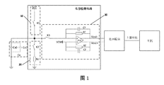
- FIG. 1 shows a schematic structural diagram of a connection between a capacitance detection circuit and a capacitance to be measured, a processing module, and a host according to an embodiment of the present application;
- FIG. 2 shows a switching control timing diagram of a capacitance detection circuit according to an embodiment of the present application
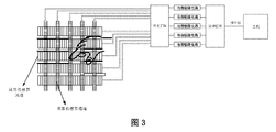
- FIG. 3 is a schematic structural diagram of a touch device in which a sensor is a stripe pattern capacitive sensor according to an embodiment of the present application;
- FIG. 4 is a schematic structural diagram of a touch device in which a sensor is a matrix pattern capacitive sensor according to an embodiment of the present application;
- FIG. 5 is a schematic structural diagram of a touch device in which a sensor is a triangular pattern pattern capacitive sensor according to an embodiment of the present application;
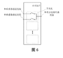
- FIG. 6 is a schematic structural diagram of a switch matrix of a touch device according to an embodiment of the present application.
- FIG. 7 is a schematic structural diagram of a processing module of a touch device according to an embodiment of the present application.
- the capacitance detection circuit includes a charging circuit 10, a discharging circuit 20, and a signal detection circuit 30.
- the charging circuit 10 is used to charge the capacitor Cx to be tested, so that the voltage difference between the two ends of the electrode plate of the capacitor Cx to be tested is a first preset voltage value;
- the discharge circuit 20 is used to cause the charged capacitor Cx to be discharged with a first charge amount after charging Where the first charge amount is less than the charge amount corresponding to the first preset voltage value;
- the signal detection circuit 30 is configured to detect the voltage value on the capacitor Cx to be measured and the second preset voltage value after being discharged through the discharge circuit 20 The voltage difference between the two to determine the capacitance change of the capacitor Cx to be measured according to the voltage difference.
- the capacitor detection circuit After the capacitor detection circuit charges the capacitor Cx to be tested through the charging circuit 10, the capacitor Cx to be tested is discharged (for example, to ground) through the discharge circuit 20, so as to release a part of the charge on the capacitor Cx to be tested, thereby avoiding passing signals.
- the detection circuit 30 detects the capacitance Cx to be measured, the signal detection circuit 30 is saturated due to the large capacitance value of the capacitance to be measured Cx and a large amount of stored charges, which cannot detect the capacitance change of the capacitance Cx to be measured.
- the following describes the detection principle of the capacitance detection circuit by using the PGA circuit (programmable gain amplifier circuit) to detect the self-capacitance of the capacitance sensor as an example:
- capacitive sensors with large self-capacitance especially capacitive sensors with a self-capacitance of 500 pF, due to their large self-capacitance and more stored charge, when they are detected by a PGA circuit, the stored charge is directly The release into the PGA circuit will saturate the PGA circuit, causing detection distortion, and the capacitance change on the capacitance sensor cannot be detected correctly.
- the amplification factor of the PGA circuit needs to be reduced. This makes the signal output by the PGA circuit weak and cannot be collected by the back-end module, which makes it impossible to correctly detect the capacitance change on the capacitance sensor.
- the capacitance detection circuit of this embodiment includes a discharge circuit 20, and the capacitance to be measured (the self-capacitance of the capacitance sensor) passes After the charging circuit 10 is charged, the discharging circuit 20 is used to release a part of the electric charge of the capacitor Cx to be tested, thereby reducing the total amount of charge on the capacitor Cx to be tested, thereby ensuring that the PGA circuit does not saturate when the capacitor Cx to be tested is detected by the PGA circuit. In this case, the amplification factor of the PGA circuit can be increased, so that the output signal can be collected and processed by the back-end module.
- the capacitance sensor is touched and its self-capacitance is increased (the capacitance of the capacitor Cx to be measured changes from Cx0 to Cx0 + Cx1), it will increase.
- the proportion of the charge corresponding to the capacitor (Cx1) in the total charge amount will increase, so that the signal strength increases, and the capacitance change of the capacitor Cx to be measured is more easily detected.
- the charging circuit 10 includes a first power source (denoted as VCC) and a first switch K1.
- a first terminal of the first switch K1 is connected to the first power source, and a second terminal of the first switch K1. Connected to the capacitor Cx to be tested to charge the capacitor Cx to be tested through the first power source VCC.
- the first power source VCC charges the capacitor Cx to be tested, so that the voltage difference between the two ends of the electrode plate of the capacitor Cx to be tested is the first preset voltage value.
- the first preset voltage value may be set to any appropriate voltage value, which is not limited in this embodiment.
- the first preset voltage value is a voltage value of the first power source VCC, or the first preset voltage value is 5V, 2V, or the like.
- the discharge circuit 20 includes a second switch K2 and a discharge resistor Rc.
- the second switch K2 and a discharge resistor Rc are connected in series.
- the discharge circuit 20 is used to discharge the capacitor Cx to be tested, thereby reducing the total amount of charge on the capacitor Cx to be tested, thereby ensuring that when the signal to be tested Cx is detected by the signal detection circuit 30, avoiding the excessive charge on the capacitor Cx to be tested.
- the signal detection circuit 30 is saturated, so that the capacitance detection circuit can be applied to detect the capacitance Cx to be measured with a large self-capacitance.
- the discharge circuit 20 causes the capacitor Cx to be discharged with a first charge amount, wherein the first charge amount can be determined as required, as long as the first charge amount is less than or equal to the first precharge
- the amount of charge corresponding to the capacitance to be measured (recorded as the total amount of charge) is sufficient.
- the first charge amount is smaller than the total charge amount.
- the first charge amount is determined according to a first preset voltage value, a second preset voltage value, and an initial capacitance value (referred to as Cx0) of the capacitance Cx to be measured.
- the first preset voltage value is greater than the second preset voltage value.
- the first charge amount (denoted as Qc) is based on a first preset voltage value (assuming that the first preset voltage value is equal to the voltage of the first power source, and the first preset voltage value is recorded as VCC) and the second preset voltage
- the product of the difference in value (denoted as VCMI) and the initial capacitance value (denoted as Cx0) is determined.
- Qc (VCC-VCMI) * Cx0.
- the first charge amount may be determined by other methods, such as manual setting or determination through experimental data analysis, or Determined by simulation experiment results, and so on.
- the signal detection circuit 30 includes a third switch K3, a programmable gain amplifier (PGA), and a feedback circuit.
- the programmable gain amplifier (PGA) has a first input terminal, a second input terminal, a first output terminal, and a second output terminal.
- the first input terminal is connected to the capacitor Cx to be measured through a third switch K3.
- the second input terminal is connected to a second power source (referred to as VCMI, and a second preset voltage value is a voltage value of the second power source).
- the first output terminal and the second output terminal are used to output a voltage signal, so as to represent a voltage difference between the voltage on the capacitor Cx to be measured after discharge and the second preset voltage value.
- the feedback circuit includes a feedback resistor Rf and a feedback capacitor Cf. The feedback circuit can adjust the amplification factor of the programmable gain amplifier. Depending on the number of outputs of the programmable gain amplifier, the feedback circuit can be one or two.
- the second preset voltage value may be determined according to requirements.
- the second preset voltage value is smaller than the first preset voltage value.
- the second preset voltage value may be 1V, 2V, or the like.
- the feedback resistor Rf and capacitor Cf will absorb the charge until the voltages at the first input terminal and the second input terminal are equal. At this time, Vout will output a positive To the voltage.
- the programmable gain amplifier PGA will discharge through the feedback resistor Rf and the feedback capacitor Cf until the voltages at the first input terminal and the second input terminal are equal. Vout will output a negative voltage.
- the process of detecting the change in the self-capacitance of the capacitor Cx to be measured using the programmable gain amplifier PGA is as follows:
- a preset capacitance value is preset, and the preset capacitance value is used as a reference for judging whether the self-capacitance changes.
- the set capacitance value may be an initial capacitance value Cx0 of the capacitance to be measured (in this embodiment, the initial capacitance value refers to the initial self-capacitance value).
- the initial capacitance value (denoted as Cx0)
- the first charge amount Qc is determined. The process is:
- the first preset voltage value is a voltage value of the first power source, which is denoted as VCC).
- the second switch K2 is controlled to be closed, the first switch K1 and the third switch K3 are opened, the capacitor Cx to be tested is discharged to the ground through the amplification resistor Rc, and the first charge amount (recorded as Qc) is released to make the voltage value on the capacitor Cx to be tested It is equal to the second preset voltage value (denoted as VCMI).
- Qc (VCC-VCMI) * Cx0.
- the signal detection circuit 30 detects the capacitance Cx to be measured.
- the specific detection process is:
- the third switch K3 When there is no change in self-capacitance: the third switch K3 is closed, and the first switch K1 and the second switch K2 are open. If the current sampling capacitance value of the capacitor Cx to be tested is equal to the set capacitance value, after the capacitor Cx to be tested is discharged, the corresponding voltage value is equal to the second preset voltage value, and the signal detection circuit 30 does not output a voltage signal. It shows that the self-capacitance of the capacitor Cx to be measured has not changed.
- the third switch K3 is closed, and the first switch K1 and the second switch K2 are opened. If the current sampling capacitance value of the capacitor Cx to be measured is greater than or less than the set capacitance value, after the capacitor Cx to be tested is discharged, the corresponding voltage value is not equal to the second preset voltage value, and the signal detection circuit 30 outputs a forward voltage signal or Negative voltage signal. It shows that the self-capacitance of the capacitor Cx to be measured has changed.
- the capacitance detection circuit works, by controlling the closing or opening of the first switch K1, the second switch K2, and the third switch K3, the capacitor Cx to be charged, discharged, or detected is controlled.
- the closing or opening of the first switch K1, the second switch K2, and the third switch K3 may be controlled by a signal in the switch control timing chart shown in FIG. 2.
- the control signal of the first switch K1 is high level, which indicates that the first switch K1 is closed
- the control signals of the second switch K2 and the third switch K3 are low level, which indicates the second switch K2. It is disconnected from the third switch K3.
- the control signal of the second switch K2 is high level, the second switch K2 is closed, and the first switch K1 and the third switch K3 are opened.
- the control signal of the third switch K3 is high level, the third switch K3 is closed, and the first switch K1 and the second switch K2 are open. This process is repeated periodically to control the opening and closing of the switch.
- the capacitance detection circuit for detecting self-capacitance can support detection of 500 pF self-capacitance, and can also support larger self-capacitance. At the same time, the performance of self-capacitance detection within 200pF has been significantly improved.
- the capacitance detection circuit can be applied to any scenario that requires capacitance detection, especially for scenarios with small capacitance changes on large self-capacitance. It can be used in various fields that require self-capacitance detection, such as self-capacitive capacitive touch and self-integrated capacitors. Self-capacitive detection in touch, self-capacitive pressure sensing, self-capacitive pressure keys, etc.
- the capacitance detection circuit can be combined with a capacitance sensor to form a touch device, which is used to detect a change in the self-capacitance of the capacitance sensor, thereby realizing detection of whether the capacitance sensor is touched, and further, it can also realize capacitance Positioning of the touched position on the sensor.
- a touch device which includes a capacitance sensor and the above-mentioned capacitance detection circuit.
- the capacitance detection circuit is electrically connected to the capacitance sensor, and performs capacitance detection on the capacitance sensor to output a voltage difference indicating a capacitance detection result. Value, the voltage difference of the capacitance detection result is used to determine the touch information acting on the capacitance sensor.
- the detection principle of whether the capacitance sensor is touched by using the capacitance detection circuit is:
- the self-capacitance of the capacitive sensor (that is, the capacitance to be measured Cx) is the initial capacitance value (referred to as Cx0).
- Cx0 the initial capacitance value
- a finger touches the capacitive sensor its self-capacitance increases, and the increased self-capacitance is recorded as Cx1.
- the capacitance detection circuit is connected to the capacitance Cx to be measured, and detects whether the capacitance Cx to be measured has a self-capacitance change, so as to determine whether there is a touch capacitance sensor such as a finger.
- the control device further includes a switch matrix (SW matrix), and the capacitance sensor is connected to the capacitance detection circuit through the switch matrix.
- the switch matrix can control the on-off between the capacitive sensor and the capacitance detection circuit, and can further control the sensor channel connected to the capacitance detection circuit in the capacitance sensor, so as to determine whether there is a touch according to the capacitance change of the detected sensor channel. And determine the touch position.
- the switch matrix includes multiple switch groups, each of which is connected to a capacitance detection circuit, and each switch group includes at least two channel control switches. Each channel control switch is correspondingly connected with a sensor channel.
- This connection method realizes the multiplexing of the capacitance detection circuit. Under the condition that all sensor channels can be detected, the number of capacitance detection circuits is reduced, thereby reducing the overall volume of the touch device. In this embodiment, as shown in FIG. 6, it multiplexes one capacitance detection circuit for two sensor channels. Of course, in other embodiments, more sensor channels can be multiplexed with a capacitance detection circuit.
- the touch device further includes a processing module, and the processing module is connected to the capacitance detection circuit to acquire and process the voltage difference output by the capacitance detection circuit.
- the processing module is used to process the voltage signal output from the capacitance detection circuit, so as to determine whether there is a touch and the coordinates of the touch position according to the voltage signal.
- the processing module includes a digitization module, a hybrid module, a coordinate calculation module, and a coordinate transmission module.
- the digitization module is used to convert the voltage difference into a digital signal, that is, to digitize the voltage difference output from the capacitance detection circuit.
- an ADC circuit is used.
- the mixed module (Mixer module) is used to demodulate the voltage amplitude of the digital signal.
- the coordinate calculation module is used to calculate the coordinates of the touch position on the capacitive sensor according to the demodulated digital signal.
- the coordinate sending module is used to send coordinates.
- this capacitance detection circuit can be applied not only to the detection of DITO OrSito strip pattern capacitance sensors (as shown in Fig. 3), but also to the matrix pattern capacitance sensors (as shown in Fig. 4) and Detection of triangular pattern capacitance sensors (as shown in Figure 5). Of course, it can be applied to the detection of capacitance sensors of other structures.
- the self-capacitance value of the capacitor Cx to be measured is the initial capacitance value Cx0.
- the charging circuit 10 charges the capacitor Cx to be measured, the first switch K1 is closed, and the second switch K2 and the third switch K3 are opened.
- the first power source VCC charges the capacitor Cx to be tested to a first preset voltage value (referred to as VCC) through the first switch K1.
- the discharge circuit 20 discharges the capacitor Cx to be measured, the second switch K2 is closed, and the first switch K1 and the third switch K3 are opened.
- the voltage value of the capacitor to be measured after discharge (denoted as U0) is equal to the second preset voltage value (denoted as VCMI), so as to ensure that no finger touches
- the output voltage difference is 0.
- the output voltage difference when the subsequent signal detection circuit 30 detects the capacitor Cx to be detected without any finger touch can be set to any appropriate value.
- the signal detection circuit 30 detects a voltage difference between the voltage value on the capacitor Cx to be measured and the second preset voltage value, the third switch K3 is closed, and the first switch K1 and the second switch K1 are open.
- the third switch K3 is closed, the voltage value on the capacitor Cx to be measured is recorded as Ux.
- the voltage value Ux is equal to the second preset value VCMI, and the voltage difference output by the signal detection circuit 30 is 0.
- the self-capacitance of the capacitor Cx to be measured will increase Cx1 and become Cx0 + Cx1. Then, when the capacitor Cx to be tested is charged by the charging circuit 10 so that the voltage value on the capacitor Cx is the first preset voltage value VCC, the amount of charge on the capacitor Cx to be measured increases compared to the amount of charge when there is no finger touch. After the charge of the first charge amount Qc is discharged through the discharge circuit 20, the amount of charge remaining on the capacitor Cx to be measured will also increase compared to the amount of charge when there is no finger touch. Accordingly, the voltage on the capacitor Cx to be tested after discharging will be corresponding.
- the transferred charge Q flows through the feedback resistor Rf in the form of a current, so that the programmable gain amplifier outputs the voltage difference value in the form of a voltage to form a voltage signal.
- the increased capacitance Cx1 is proportional to the output voltage signal.
- the subsequent processing module can obtain the voltage signal, and can determine whether there is an increased capacitance Cx1 and its size according to the voltage signal change, and then determine whether there is a touch operation on the capacitance sensor.
- the bar-shaped capacitive sensor generally refers to a channel with several lateral sensors (Sensors, such as ITO / bottom shown in FIG. 3), It has several longitudinal sensor (Sensor, ITO / TOP) channels as shown in Figure 3. It can be two layers of sensor channels stacked one on top of the other, or a layer of sensor channels can be interconnected by punching holes. .
- the horizontal sensor channel and the vertical sensor channel are connected to the capacitance detection circuit to realize the detection of the channel self-capacitance.
- the switch matrix can control the sensor channels detected at any time. For example, the horizontal sensor channel is detected at a certain moment, and the vertical sensor channel is detected at the next moment.
- the touch coordinates of the finger can be calculated according to the changed channel, thereby determining the touch position. The calculated touch coordinates can be reported to the host.
- a terminal device which includes the above-mentioned touch device.
- the capacitance detection circuit of the touch device in the terminal device charges the self-capacitance, and then uses the discharge circuit 20 to release a part of the electric charge to ensure that the self-capacitance increases, that is, when the capacitance value of the self-capacitance changes, the increase amount
- the corresponding charge amount can be transferred through the signal detection circuit 30 (such as the PGA circuit) in the subsequent stage and converted into a voltage signal without causing the signal detection circuit 30 to saturate. This enables the detection of a capacitor with a large self-capacitance value, which improves Adaptability.
Landscapes
- Engineering & Computer Science (AREA)
- General Engineering & Computer Science (AREA)
- Theoretical Computer Science (AREA)
- Physics & Mathematics (AREA)
- General Physics & Mathematics (AREA)
- Human Computer Interaction (AREA)
- Electronic Switches (AREA)
- Measurement Of Resistance Or Impedance (AREA)
Abstract
The embodiment of the present application provides a capacitance detection circuit, a touch device and a terminal device. The capacitance detection circuit comprises: a charging circuit configured to charge a to-be-detected capacitor such that a voltage difference of two ends of a pole plate of the to-be-detected capacitor is a first preset voltage value; a discharge circuit configured to make the charged to-be-detected capacitor release a quantity of first electric charges, wherein the quantity of first electric charges is less than a quantity of electric charges corresponding to the first preset voltage value; and a signal detection circuit used for detecting a voltage difference between a voltage value of the to-be-detected capacitor after being discharged by the discharge circuit and a second preset voltage value to determine a capacitance value variation of the to-be-detected capacitor according to the voltage difference. The capacitance detection circuit can perform capacitance detection when self-capacitance is high.
Description
本申请实施例涉及检测技术领域,尤其涉及一种电容检测电路、触控装置及终端设备。The embodiments of the present application relate to the field of detection technology, and in particular, to a capacitance detection circuit, a touch device, and a terminal device.
近年来,随着智能移动终端的普及,对电容式触摸屏的性能需求越来越高,相应地,对电容式触摸屏的检测要求,尤其是对电容式触摸屏的自电容检测的要求也越来越高。In recent years, with the popularity of smart mobile terminals, the performance requirements for capacitive touch screens have become increasingly high. Correspondingly, the requirements for the detection of capacitive touch screens, especially for the self-capacitance detection of capacitive touch screens, have become more and more demanding. high.
现有技术中,对自电容的架构性能较差。而随着电容式触控屏的发展,电容传感器(sensor)的自电容越来越大,从最开始50pF以内,慢慢增加到100pF、到现在主流200pF以及最新的电容传感器的自电容已经高达500pF。随着电容传感器的升高,电容传感器被触摸(touch)时产生的自电容反而极大地减小。如,自电容为50pF的电容传感器在被触摸时产生的自电容为1pF,而自电容为500pF的电容传感器在被触摸时产生的自电容为0.2pF。这使得自电容较大的电容传感器在被触摸时产生的电容变化信号极小,不能被现有的自电容架构所检测到。In the prior art, the performance of the self-capacitor architecture is poor. With the development of capacitive touch screens, the self-capacitance of capacitive sensors has become larger and larger, from 50pF at the beginning to slowly increase to 100pF, to the current mainstream 200pF and the latest self-capacitance of capacitive sensors has reached as high as 500pF. With the increase of the capacitance sensor, the self-capacitance generated when the capacitance sensor is touched is greatly reduced. For example, a self-capacitance sensor with a self-capacitance of 50 pF generates a self-capacitance when touched, and a self-capacitance sensor with a self-capacitance of 500 pF generates a self-capacitance when touched is 0.2 pF. This makes a capacitance sensor with a large self-capacitance generate a very small capacitance change signal when it is touched, which cannot be detected by the existing self-capacitance architecture.
现有自电容架构仅能较好地支持对50pF的自电容的检测,最大勉强能够支持200pF左右自电容的检测,对于具有500pF的自电容的电容传感器,由于检测精度限制,现有的检测电路无法进行支持。The existing self-capacitance architecture can only support the detection of self-capacitance of 50 pF, and it can barely support the detection of self-capacitance of about 200 pF. For a capacitance sensor with a self-capacitance of 500 pF, due to the limitation of detection accuracy, the existing detection circuit Unable to support.
发明内容Summary of the Invention
有鉴于此,本申请实施例所解决的技术问题之一在于提供一种电容检测电路、触控装置及终端设备,用以克服现有技术中自电容较大时不能进行电容检测的问题。In view of this, one of the technical problems solved by the embodiments of the present application is to provide a capacitance detection circuit, a touch device, and a terminal device to overcome the problem that the capacitance detection cannot be performed when the self-capacitance is large in the prior art.
本申请实施例提供一种电容检测电路,其包括:充电电路,用于对待测电容充电,使待测电容的极板两端的电压差值为第一预设电压值;放电电路,用于使充电后的待测电容释放第一电荷量的电荷,其中,第一电荷量小于第一预设电压值对应的电荷量;信号检测电路,用于检测通过放电电路放电后的待测电容上的电压值与第二预设电压值之间的电压差值,以根据电压差值 确定待测电容的电容值变化量。An embodiment of the present application provides a capacitance detection circuit, which includes: a charging circuit for charging the capacitor to be measured so that a voltage difference between two ends of an electrode plate of the capacitor to be measured is a first preset voltage value; and a discharging circuit for enabling The charged capacitor under test releases a charge of a first charge amount, where the first charge amount is less than the charge amount corresponding to the first preset voltage value; a signal detection circuit is used to detect the capacitance of the capacitor under test after being discharged through the discharge circuit. A voltage difference between the voltage value and the second preset voltage value, so as to determine a capacitance value change amount of the capacitor to be measured according to the voltage difference value.
可选地,第一电荷量根据第一预设电压值、第二预设电压值和待测电容的初始电容值确定,第一预设电压值大于第二预设电压值。Optionally, the first charge amount is determined according to the first preset voltage value, the second preset voltage value, and an initial capacitance value of the capacitor to be measured, and the first preset voltage value is greater than the second preset voltage value.
可选地,第一电荷量根据第一预设电压值与第二预设电压值的差和初始电容值的乘积确定。Optionally, the first charge amount is determined according to a product of a difference between the first preset voltage value and the second preset voltage value and an initial capacitance value.
可选地,充电电路包括第一开关,放电电路包括第二开关,信号检测电路包括第三开关,充电电路对待测电容充电时,第一开关闭合,第二开关和第三开关断开;放电电路使待测电容放电时,第二开关闭合,第一开关和第三开关断开;信号检测电路检测待测电容上的电压值与第二预设电压值之间的电压差值时,第三开关闭合,第一开关和第二开关断开。Optionally, the charging circuit includes a first switch, the discharging circuit includes a second switch, and the signal detection circuit includes a third switch. When the charging circuit charges the capacitor to be measured, the first switch is closed, and the second switch and the third switch are open; When the circuit discharges the capacitor to be tested, the second switch is closed, and the first switch and the third switch are opened. When the signal detection circuit detects a voltage difference between the voltage value on the capacitor to be tested and the second preset voltage value, the first The three switches are closed, and the first switch and the second switch are open.
可选地,当第三开关闭合时,若待测电容的当前采样电容值等于设定电容值,则待测电容放电后,对应的电压值与第二预设电压值相等;当第三开关闭合时,若待测电容的当前采样电容值大于或小于设定电容值,则待测电容放电后,对应的电压值与第二预设电压值不相等。Optionally, when the third switch is closed, if the current sampling capacitance value of the capacitor under test is equal to the set capacitance value, after the capacitor under test is discharged, the corresponding voltage value is equal to the second preset voltage value; when the third switch is When closed, if the current sampling capacitance value of the capacitor under test is greater than or less than the set capacitance value, after the capacitor under test is discharged, the corresponding voltage value is not equal to the second preset voltage value.
可选地,设定电容值等于待测电容的初始电容值。Optionally, the set capacitance value is equal to the initial capacitance value of the capacitance to be measured.
可选地,放电电路还包括放电电阻,放电电阻的第一端与第二开关连接,放电电路的第二端接地;当第二开关闭合时,待测电容通过放电电阻对地放电。Optionally, the discharge circuit further includes a discharge resistor. The first end of the discharge resistor is connected to the second switch, and the second end of the discharge circuit is grounded. When the second switch is closed, the capacitor to be tested is discharged to the ground through the discharge resistor.
本申请实施例还一种触控装置,其包括电容传感器及上述的电容检测电路;电容检测电路与电容传感器电连接,并对电容传感器进行电容检测,输出指示电容检测结果的电压差值,电容检测结果的电压差值用于确定作用于电容传感器上的触控信息。An embodiment of the present application further provides a touch device, which includes a capacitance sensor and the above-mentioned capacitance detection circuit. The capacitance detection circuit is electrically connected to the capacitance sensor, and performs capacitance detection on the capacitance sensor, and outputs a voltage difference indicating a capacitance detection result. The voltage difference of the detection result is used to determine the touch information acting on the capacitive sensor.
可选地,触控装置还包括开关矩阵,电容传感器通过开关矩阵与电容检测电路连接。Optionally, the touch device further includes a switch matrix, and the capacitance sensor is connected to the capacitance detection circuit through the switch matrix.
可选地,电容传感器包括多个传感器通道;开关矩阵包括多个开关组,各开关组对应连接一个电容检测电路,各开关组内包括至少两个通道控制开关,各通道控制开关对应连接有一个传感器通道。Optionally, the capacitance sensor includes a plurality of sensor channels; the switch matrix includes a plurality of switch groups, each switch group is correspondingly connected to a capacitance detection circuit, each switch group includes at least two channel control switches, and each channel control switch is correspondingly connected to one Sensor channel.
可选地,触控装置还包括处理模块,处理模块与电容检测电路连接,获取并处理电容检测电路输出的电压差值。Optionally, the touch device further includes a processing module, and the processing module is connected to the capacitance detection circuit to acquire and process the voltage difference output by the capacitance detection circuit.
可选地,处理模块包括:数字化模块,用于将电压差值转化为数字信号; 混合模块,用于对数字信号进行电压幅度解调;坐标计算模块,用于根据解调后的数字信号计算电容传感器上的触控位置的坐标;坐标发送模块,用于发送坐标。Optionally, the processing module includes: a digitizing module for converting the voltage difference into a digital signal; a mixing module for demodulating the voltage amplitude of the digital signal; and a coordinate calculation module for calculating the demodulated digital signal The coordinates of the touch position on the capacitive sensor; the coordinate sending module is used to send the coordinates.
本申请实施例还提供一种终端设备,其包括上述的触控装置。An embodiment of the present application further provides a terminal device including the above-mentioned touch device.
由以上技术方案可见,本申请实施例的电容检测电路,在通过充电电路对待测电容进行充电后,通过放电电路使待测电容放电(例如,对地放电),以将待测电容上的部分电荷释放,从而避免通过信号检测电路对待测电容进行检测时,由于待测电容的电容值较大,存储的电荷量较多,造成信号检测电路饱和,不能对待测电容的电容变化进行检测的问题。As can be seen from the above technical solutions, the capacitance detection circuit in the embodiment of the present application, after charging the capacitor to be tested through the charging circuit, discharges the capacitor to be tested (for example, discharging to ground) through the discharge circuit, so as to part of the capacitor to be tested Charge release, thereby avoiding the problem that when the capacitance to be measured is detected by the signal detection circuit, the capacitance of the capacitance to be measured is large and the amount of stored charges is large, causing the signal detection circuit to saturate, and the capacitance change of the capacitance to be measured cannot be detected. .
为了更清楚地说明本申请实施例或现有技术中的技术方案,下面将对实施例或现有技术描述中所需要使用的附图作简单地介绍,显而易见地,下面描述中的附图仅仅是本申请的一些实施例,对于本领域技术人员来讲,在不付出创造性劳动性的前提下,还可以根据这些附图获得其他的附图。In order to explain the technical solutions in the embodiments of the present application or the prior art more clearly, the drawings used in the description of the embodiments or the prior art will be briefly introduced below. Obviously, the drawings in the following description are merely These are some embodiments of the present application. For those skilled in the art, other drawings can be obtained based on these drawings without paying creative labor.
图1示出了根据本申请的实施例的电容检测电路与待测电容、处理模块及主机连接的结构示意图;FIG. 1 shows a schematic structural diagram of a connection between a capacitance detection circuit and a capacitance to be measured, a processing module, and a host according to an embodiment of the present application; FIG.
图2示出了根据本申请的实施例的电容检测电路的开关控制时序图;FIG. 2 shows a switching control timing diagram of a capacitance detection circuit according to an embodiment of the present application; FIG.
图3示出了根据本申请的实施例的传感器为条形图案电容传感器的触控装置的结构示意图;FIG. 3 is a schematic structural diagram of a touch device in which a sensor is a stripe pattern capacitive sensor according to an embodiment of the present application; FIG.
图4示出了根据本申请的实施例的传感器为矩阵式图案电容传感器的触控装置的结构示意图;4 is a schematic structural diagram of a touch device in which a sensor is a matrix pattern capacitive sensor according to an embodiment of the present application;
图5示出了根据本申请的实施例的传感器为三角Pattern图案电容传感器的触控装置的结构示意图;5 is a schematic structural diagram of a touch device in which a sensor is a triangular pattern pattern capacitive sensor according to an embodiment of the present application;
图6示出了根据本申请的实施例的触控装置的开关矩阵的结构示意图;6 is a schematic structural diagram of a switch matrix of a touch device according to an embodiment of the present application;
图7示出了根据本申请的实施例的触控装置的处理模块的结构示意图。FIG. 7 is a schematic structural diagram of a processing module of a touch device according to an embodiment of the present application.
为使得本申请实施例的发明目的、特征、优点能够更加的明显和易懂,下面将结合本申请实施例中的附图,对本申请实施例中的技术方案进行清楚、完整地描述,显然,所描述的实施例仅仅是本申请实施例一部分实施例,而 非全部实施例。基于本申请中的实施例,本领域普通技术人员在没有做出创造性劳动前提下所获得的所有其他实施例,都属于本申请实施例保护的范围。In order to make the objects, features, and advantages of the embodiments of the present application more obvious and understandable, the technical solutions in the embodiments of the present application will be clearly and completely described in combination with the drawings in the embodiments of the present application. Obviously, The described embodiments are only a part of the embodiments of the present application, but not all the embodiments. Based on the embodiments in the present application, all other embodiments obtained by a person of ordinary skill in the art without creative efforts shall fall within the protection scope of the embodiments of the present application.
下面结合本申请实施例附图进一步说明本申请实施例具体实现。The specific implementation of the embodiment of the present application will be further described below with reference to the accompanying drawings of the embodiment of the present application.
如图1所示,电容检测电路包括充电电路10、放电电路20和信号检测电路30。充电电路10用于对待测电容Cx充电,使待测电容Cx的极板两端的电压差值为第一预设电压值;放电电路20用于使充电后的待测电容Cx释放第一电荷量的电荷,其中,第一电荷量小于第一预设电压值对应的电荷量;信号检测电路30用于检测通过放电电路20放电后的待测电容Cx上的电压值与第二预设电压值之间的电压差值,以根据电压差值确定待测电容Cx的电容值变化量。As shown in FIG. 1, the capacitance detection circuit includes a charging circuit 10, a discharging circuit 20, and a signal detection circuit 30. The charging circuit 10 is used to charge the capacitor Cx to be tested, so that the voltage difference between the two ends of the electrode plate of the capacitor Cx to be tested is a first preset voltage value; the discharge circuit 20 is used to cause the charged capacitor Cx to be discharged with a first charge amount after charging Where the first charge amount is less than the charge amount corresponding to the first preset voltage value; the signal detection circuit 30 is configured to detect the voltage value on the capacitor Cx to be measured and the second preset voltage value after being discharged through the discharge circuit 20 The voltage difference between the two to determine the capacitance change of the capacitor Cx to be measured according to the voltage difference.
该电容检测电路通过充电电路10对待测电容Cx进行充电后,通过放电电路20使待测电容Cx放电(例如,对地放电),以将待测电容Cx上的部分电荷释放,从而避免通过信号检测电路30对待测电容Cx进行检测时,由于待测电容Cx的电容值较大,存储的电荷量较多,造成信号检测电路30饱和,不能对待测电容Cx的电容变化进行检测的问题。After the capacitor detection circuit charges the capacitor Cx to be tested through the charging circuit 10, the capacitor Cx to be tested is discharged (for example, to ground) through the discharge circuit 20, so as to release a part of the charge on the capacitor Cx to be tested, thereby avoiding passing signals. When the detection circuit 30 detects the capacitance Cx to be measured, the signal detection circuit 30 is saturated due to the large capacitance value of the capacitance to be measured Cx and a large amount of stored charges, which cannot detect the capacitance change of the capacitance Cx to be measured.
下面结合图1,以通过PGA电路(可编程增益放大电路)对电容传感器的自电容进行检测为例,对电容检测电路的检测原理进行说明:The following describes the detection principle of the capacitance detection circuit by using the PGA circuit (programmable gain amplifier circuit) to detect the self-capacitance of the capacitance sensor as an example:
针对自电容较大的电容传感器(电容sensor),尤其是自电容在500pF的电容传感器,由于其自电容较大,存储的电荷较多,在通过PGA电路对其进行检测时,存储的电荷直接释放到PGA电路中会使PGA电路饱和,造成检测失真,无法正确检测电容传感器上的电容变化。为了防止PGA电路饱和,需要降低PGA电路的放大倍数,这就使得PGA电路输出的信号微弱,不能被后端模块采集,致使无法正确检测电容传感器上的电容变化。For capacitive sensors with large self-capacitance (capacitive sensors), especially capacitive sensors with a self-capacitance of 500 pF, due to their large self-capacitance and more stored charge, when they are detected by a PGA circuit, the stored charge is directly The release into the PGA circuit will saturate the PGA circuit, causing detection distortion, and the capacitance change on the capacitance sensor cannot be detected correctly. In order to prevent the PGA circuit from being saturated, the amplification factor of the PGA circuit needs to be reduced. This makes the signal output by the PGA circuit weak and cannot be collected by the back-end module, which makes it impossible to correctly detect the capacitance change on the capacitance sensor.
为了能够在PGA电路不饱和的情况下,获得可用的能够确定电容传感器的电容变化的信号,本实施例的电容检测电路中包括了放电电路20,在待测电容(电容传感器的自电容)通过充电电路10充电后,利用放电电路20使待测电容Cx释放一部分电荷,减少待测电容Cx上的电荷总量,从而保证在通过PGA电路对待测电容Cx进行检测时不会出现PGA电路饱和的情况,进而可以将PGA电路的放大倍数增高,使其输出的信号能够被后端模块采集和处 理。In order to obtain a signal that can determine the capacitance change of the capacitance sensor when the PGA circuit is not saturated, the capacitance detection circuit of this embodiment includes a discharge circuit 20, and the capacitance to be measured (the self-capacitance of the capacitance sensor) passes After the charging circuit 10 is charged, the discharging circuit 20 is used to release a part of the electric charge of the capacitor Cx to be tested, thereby reducing the total amount of charge on the capacitor Cx to be tested, thereby ensuring that the PGA circuit does not saturate when the capacitor Cx to be tested is detected by the PGA circuit. In this case, the amplification factor of the PGA circuit can be increased, so that the output signal can be collected and processed by the back-end module.
此外,由于释放了一部分电荷,使待测电容Cx上的电荷总量降低,如果电容传感器被触摸造成其自电容增大(待测电容Cx的电容由Cx0变为Cx0+Cx1),则增大的电容(Cx1)对应的电荷在总电荷量上的占比将增加,从而使得信号强度增加,使得待测电容Cx的电容变化更容易被检测到。In addition, because a part of the charge is released, the total amount of charge on the capacitor Cx to be measured is reduced. If the capacitance sensor is touched and its self-capacitance is increased (the capacitance of the capacitor Cx to be measured changes from Cx0 to Cx0 + Cx1), it will increase. The proportion of the charge corresponding to the capacitor (Cx1) in the total charge amount will increase, so that the signal strength increases, and the capacitance change of the capacitor Cx to be measured is more easily detected.
下面结合图1,对本实施例中的电容检测电路进行具体说明:The following describes the capacitance detection circuit in this embodiment with reference to FIG. 1 in detail:
关于充电电路10,如图1所示,充电电路10包括第一电源(记作VCC)和第一开关K1,第一开关K1第一端与第一电源连接,第一开关K1的第二端与待测电容Cx连接,以通过第一电源VCC对待测电容Cx充电。Regarding the charging circuit 10, as shown in FIG. 1, the charging circuit 10 includes a first power source (denoted as VCC) and a first switch K1. A first terminal of the first switch K1 is connected to the first power source, and a second terminal of the first switch K1. Connected to the capacitor Cx to be tested to charge the capacitor Cx to be tested through the first power source VCC.
具体地,在本实施例中,第一电源VCC对待测电容Cx充电,使待测电容Cx的极板两端的电压差值为第一预设电压值。需要说明的是,根据检测需要的不同,第一预设电压值可以设置为任意适当的电压值,本实施例对此不作限定。例如,第一预设电压值为第一电源VCC的电压值,或者,第一预设电压值为5V、2V等。Specifically, in this embodiment, the first power source VCC charges the capacitor Cx to be tested, so that the voltage difference between the two ends of the electrode plate of the capacitor Cx to be tested is the first preset voltage value. It should be noted that, according to different detection needs, the first preset voltage value may be set to any appropriate voltage value, which is not limited in this embodiment. For example, the first preset voltage value is a voltage value of the first power source VCC, or the first preset voltage value is 5V, 2V, or the like.
关于放电电路20,在本实施例中,放电电路20包括第二开关K2和放电电阻Rc第二开关K2和放电电阻Rc串联。放电电路20用于使待测电容Cx放电,从而降低待测电容Cx上的电荷总量,进而保证通过信号检测电路30对待测电容Cx进行检测时,避免由于待测电容Cx上的电荷量过多而是信号检测电路30饱和,从而使该电容检测电路能够应用于对自电容较大的待测电容Cx进行检测。Regarding the discharge circuit 20, in this embodiment, the discharge circuit 20 includes a second switch K2 and a discharge resistor Rc. The second switch K2 and a discharge resistor Rc are connected in series. The discharge circuit 20 is used to discharge the capacitor Cx to be tested, thereby reducing the total amount of charge on the capacitor Cx to be tested, thereby ensuring that when the signal to be tested Cx is detected by the signal detection circuit 30, avoiding the excessive charge on the capacitor Cx to be tested. Mostly, the signal detection circuit 30 is saturated, so that the capacitance detection circuit can be applied to detect the capacitance Cx to be measured with a large self-capacitance.
具体地,在本实施例中,放电电路20使待测电容Cx释放第一电荷量的电荷,其中,第一电荷量可以根据需要确定,只要保证第一电荷量小于或等于充电至第一预设电压值时待测电容对应的电荷量(记作总电荷量)即可。Specifically, in this embodiment, the discharge circuit 20 causes the capacitor Cx to be discharged with a first charge amount, wherein the first charge amount can be determined as required, as long as the first charge amount is less than or equal to the first precharge When the voltage value is set, the amount of charge corresponding to the capacitance to be measured (recorded as the total amount of charge) is sufficient.
优选地,第一电荷量小于总电荷量,例如,第一电荷量根据第一预设电压值、第二预设电压值和待测电容Cx的初始电容值(记作Cx0)确定。在本实施例中,为了便于检测,第一预设电压值大于第二预设电压值。Preferably, the first charge amount is smaller than the total charge amount. For example, the first charge amount is determined according to a first preset voltage value, a second preset voltage value, and an initial capacitance value (referred to as Cx0) of the capacitance Cx to be measured. In this embodiment, in order to facilitate detection, the first preset voltage value is greater than the second preset voltage value.
具体地,第一电荷量(记作Qc)根据第一预设电压值(设第一预设电压值等于第一电源的电压,第一预设电压值记作VCC)与第二预设电压值(记作VCMI)的差和初始电容值(记作Cx0)的乘积确定。换而言之Qc=(VCC-VCMI)*Cx0。Specifically, the first charge amount (denoted as Qc) is based on a first preset voltage value (assuming that the first preset voltage value is equal to the voltage of the first power source, and the first preset voltage value is recorded as VCC) and the second preset voltage The product of the difference in value (denoted as VCMI) and the initial capacitance value (denoted as Cx0) is determined. In other words, Qc = (VCC-VCMI) * Cx0.
当然,本实施例仅是例举了一种优选地第一电荷量确定方式,在其他实施例中,第一电荷量可以采用其他方式确定,如,人工设定或通过实验数据分析确定,或通过仿真实验结果确定,等等。Of course, this embodiment merely exemplifies a preferred method for determining the first charge amount. In other embodiments, the first charge amount may be determined by other methods, such as manual setting or determination through experimental data analysis, or Determined by simulation experiment results, and so on.
关于信号检测电路30,在本实施例中,信号检测电路30包括第三开关K3、可编程增益放大器(PGA)和反馈电路。其中,可编程增益放大器(PGA)具有第一输入端、第二输入端、第一输出端和第二输出端。第一输入端通过第三开关K3与待测电容Cx连接。第二输入端与第二电源(记作VCMI,设第二预设电压值为第二电源的电压值)连接。第一输出端和第二输出端用于输出电压信号,以表征放电后的待测电容Cx上的电压与第二预设电压值之间的电压差值。反馈电路包括反馈电阻Rf和反馈电容Cf,反馈电路可以用调节可编程增益放大器的放大倍数。根据可编程增益放大器的输出端数量不同,反馈电路可以是一组或两组。Regarding the signal detection circuit 30, in the present embodiment, the signal detection circuit 30 includes a third switch K3, a programmable gain amplifier (PGA), and a feedback circuit. The programmable gain amplifier (PGA) has a first input terminal, a second input terminal, a first output terminal, and a second output terminal. The first input terminal is connected to the capacitor Cx to be measured through a third switch K3. The second input terminal is connected to a second power source (referred to as VCMI, and a second preset voltage value is a voltage value of the second power source). The first output terminal and the second output terminal are used to output a voltage signal, so as to represent a voltage difference between the voltage on the capacitor Cx to be measured after discharge and the second preset voltage value. The feedback circuit includes a feedback resistor Rf and a feedback capacitor Cf. The feedback circuit can adjust the amplification factor of the programmable gain amplifier. Depending on the number of outputs of the programmable gain amplifier, the feedback circuit can be one or two.
需要说明的是,第二预设电压值可以根据需要确定。在本实施例中,第二预设电压值小于第一预设电压值。例如,第二预设电压值可以为1V、2V等。It should be noted that the second preset voltage value may be determined according to requirements. In this embodiment, the second preset voltage value is smaller than the first preset voltage value. For example, the second preset voltage value may be 1V, 2V, or the like.
通过可编程增益放大器对待测电容Cx进行检测和信号放大的原理为:The principle of detecting and signal amplification of the capacitor Cx to be measured through a programmable gain amplifier is:
若第一输入端输入的电压与第二输入端输入的电压相等,则反馈电阻Rf和反馈电容Cf不会释放电荷,也不会吸收电荷,可编程增益放大器PGA的差分输出(Vout+)-(Vout-)=0V,故无电压信号输出。If the voltage input at the first input terminal is equal to the voltage input at the second input terminal, the feedback resistor Rf and the feedback capacitor Cf will not release or absorb charges. The differential output of the programmable gain amplifier PGA (Vout +)-( Vout-) = 0V, so no voltage signal is output.
若第一输入端输入的电压比第二输入端输入的电压大,则反馈电阻Rf和电容Cf会吸收电荷,直到第一输入端和第二输入端的电压相等,此时,Vout会输出一个正向的电压。If the voltage input at the first input terminal is greater than the voltage input at the second input terminal, the feedback resistor Rf and capacitor Cf will absorb the charge until the voltages at the first input terminal and the second input terminal are equal. At this time, Vout will output a positive To the voltage.
若第一输入端输入的电压比第二输入端输入的电压小,则可编程增益放大器PGA会通过反馈电阻Rf和反馈电容Cf放电,直到第一输入端和第二输入端电压相等,此时,Vout会输出一个负向的电压。If the voltage input at the first input terminal is lower than the voltage input at the second input terminal, the programmable gain amplifier PGA will discharge through the feedback resistor Rf and the feedback capacitor Cf until the voltages at the first input terminal and the second input terminal are equal. Vout will output a negative voltage.
根据此原理利用可编程增益放大器PGA对待测电容Cx的自电容变化进行检测的过程如下:According to this principle, the process of detecting the change in the self-capacitance of the capacitor Cx to be measured using the programmable gain amplifier PGA is as follows:
预设一个设定电容值,该预设的设定电容值作为判断自电容是否变化的基准。为了便于检测,该设定电容值可以为待测电容的初始电容值Cx0(本实施例中,初始电容值指初始自电容值)。A preset capacitance value is preset, and the preset capacitance value is used as a reference for judging whether the self-capacitance changes. To facilitate detection, the set capacitance value may be an initial capacitance value Cx0 of the capacitance to be measured (in this embodiment, the initial capacitance value refers to the initial self-capacitance value).
在确定待测电容Cx的自电容值为初始电容值(记作Cx0)时,确定第一 电荷量Qc。其过程为:When the self-capacitance value of the capacitor Cx to be measured is determined as the initial capacitance value (denoted as Cx0), the first charge amount Qc is determined. The process is:
控制第一开关K1闭合,第二开关K2和第三开关K3断开,第一电源VCC通过充电电路10对待测电容Cx充电,使其上的电压值为第一预设电压值(这里设定第一预设电压值为第一电源的电压值,记作VCC)。此时,待测电容Cx上的电荷量(记作Qx),Qx=VCC*Cx0。Control the first switch K1 to be closed, the second switch K2 and the third switch K3 to be opened, and the first power source VCC to charge the capacitor Cx to be measured through the charging circuit 10 so that the voltage value on the first switch V1 is set to the first preset voltage value (set here The first preset voltage value is a voltage value of the first power source, which is denoted as VCC). At this time, the amount of charge on the capacitor Cx to be measured (denoted as Qx), Qx = VCC * Cx0.
控制第二开关K2闭合,第一开关K1和第三开关K3断开,待测电容Cx通过放大电阻Rc对地放电,释放第一电荷量(记作Qc)使待测电容Cx上的电压值等于第二预设电压值(记作VCMI)。此时,Qc=(VCC-VCMI)*Cx0。The second switch K2 is controlled to be closed, the first switch K1 and the third switch K3 are opened, the capacitor Cx to be tested is discharged to the ground through the amplification resistor Rc, and the first charge amount (recorded as Qc) is released to make the voltage value on the capacitor Cx to be tested It is equal to the second preset voltage value (denoted as VCMI). At this time, Qc = (VCC-VCMI) * Cx0.
通过信号检测电路30对待测电容Cx进行检测。具体检测过程为:The signal detection circuit 30 detects the capacitance Cx to be measured. The specific detection process is:
自电容无变化时:第三开关K3闭合,第一开关K1和第二开关K2断开。若待测电容Cx的当前采样电容值等于设定电容值,则待测电容Cx放电后,对应的电压值与第二预设电压值相等,信号检测电路30不输出电压信号。说明待测电容Cx的自电容值无变化。When there is no change in self-capacitance: the third switch K3 is closed, and the first switch K1 and the second switch K2 are open. If the current sampling capacitance value of the capacitor Cx to be tested is equal to the set capacitance value, after the capacitor Cx to be tested is discharged, the corresponding voltage value is equal to the second preset voltage value, and the signal detection circuit 30 does not output a voltage signal. It shows that the self-capacitance of the capacitor Cx to be measured has not changed.
自电容变化时:第三开关K3闭合,第一开关K1和第二开关K2断开。若待测电容Cx的当前采样电容值大于或小于设定电容值,则待测电容Cx放电后,对应的电压值与第二预设电压值不相等,信号检测电路30输出正向电压信号或负向电压信号。说明待测电容Cx的自电容值有变化。When the self-capacitance changes: the third switch K3 is closed, and the first switch K1 and the second switch K2 are opened. If the current sampling capacitance value of the capacitor Cx to be measured is greater than or less than the set capacitance value, after the capacitor Cx to be tested is discharged, the corresponding voltage value is not equal to the second preset voltage value, and the signal detection circuit 30 outputs a forward voltage signal or Negative voltage signal. It shows that the self-capacitance of the capacitor Cx to be measured has changed.
需要说明的是,该电容检测电路工作时,通过控制第一开关K1、第二开关K2和第三开关K3的闭合或断开,控制对待测电容Cx进行充电、放电或检测。具体地,第一开关K1、第二开关K2和第三开关K3的闭合或断开可以通过如图2所示的开关控制时序图中的信号控制。例如,在t1时间段内,第一开关K1的控制信号为高电平,则指示第一开关K1闭合,第二开关K2和第三开关K3的控制信号为低电平,指示第二开关K2和第三开关K3断开。同理,在t2时间段内,第二开关K2的控制信号为高电平,第二开关K2闭合,第一开关K1和第三开关K3断开。在t3时间段内,第三开关K3的控制信号为高电平,第三开关K3闭合,第一开关K1和第二开关K2断开。以此过程周期性重复,进行开关的断开与闭合的控制。It should be noted that when the capacitance detection circuit works, by controlling the closing or opening of the first switch K1, the second switch K2, and the third switch K3, the capacitor Cx to be charged, discharged, or detected is controlled. Specifically, the closing or opening of the first switch K1, the second switch K2, and the third switch K3 may be controlled by a signal in the switch control timing chart shown in FIG. 2. For example, during the time period t1, the control signal of the first switch K1 is high level, which indicates that the first switch K1 is closed, and the control signals of the second switch K2 and the third switch K3 are low level, which indicates the second switch K2. It is disconnected from the third switch K3. Similarly, during the time period t2, the control signal of the second switch K2 is high level, the second switch K2 is closed, and the first switch K1 and the third switch K3 are opened. During the time period of t3, the control signal of the third switch K3 is high level, the third switch K3 is closed, and the first switch K1 and the second switch K2 are open. This process is repeated periodically to control the opening and closing of the switch.
该对自电容进行检测的电容检测电路能够支持对500pF的自电容的检测,还可以支持更大自电容。同时对于200pF以内的自电容检测有性能的显著提升。The capacitance detection circuit for detecting self-capacitance can support detection of 500 pF self-capacitance, and can also support larger self-capacitance. At the same time, the performance of self-capacitance detection within 200pF has been significantly improved.
该电容检测电路可以适用任何需要电容检测的场景,尤其适用大自电容上有小电容变化的场景,可以用于各种需要自电容检测领域,例如自容式电容触控、自互一体式电容触控中的自容检测、自容式压力感应、自容式压力按键等。The capacitance detection circuit can be applied to any scenario that requires capacitance detection, especially for scenarios with small capacitance changes on large self-capacitance. It can be used in various fields that require self-capacitance detection, such as self-capacitive capacitive touch and self-integrated capacitors. Self-capacitive detection in touch, self-capacitive pressure sensing, self-capacitive pressure keys, etc.
如图3所示,该电容检测电路可以与电容传感器组合,形成触控装置,用于对电容传感器的自电容变化进行检测,从而实现对电容传感器是否被触摸的检测,进一步还可以实现对电容传感器上被触摸位置的定位。As shown in FIG. 3, the capacitance detection circuit can be combined with a capacitance sensor to form a touch device, which is used to detect a change in the self-capacitance of the capacitance sensor, thereby realizing detection of whether the capacitance sensor is touched, and further, it can also realize capacitance Positioning of the touched position on the sensor.
根据本申请的另一方面,提供一种触控装置,其包括电容传感器及上述的电容检测电路,电容检测电路与电容传感器电连接,并对电容传感器进行电容检测输出指示电容检测结果的电压差值,电容检测结果的电压差值用于确定作用于电容传感器上的触控信息。According to another aspect of the present application, a touch device is provided, which includes a capacitance sensor and the above-mentioned capacitance detection circuit. The capacitance detection circuit is electrically connected to the capacitance sensor, and performs capacitance detection on the capacitance sensor to output a voltage difference indicating a capacitance detection result. Value, the voltage difference of the capacitance detection result is used to determine the touch information acting on the capacitance sensor.
利用该电容检测电路对电容传感器是否被触摸的检测原理为:The detection principle of whether the capacitance sensor is touched by using the capacitance detection circuit is:
在无手指(或其他物体)触摸触控装置(如触控屏幕)的电容传感器时,电容传感器的自电容(即待测电容Cx)为初始电容值(记作Cx0)。当有手指触摸电容传感器时,其自电容增大,增大的自电容记作Cx1。该电容检测电路通过与待测电容Cx连接,检测待测电容Cx是否有自电容变化,即可确定是否有手指等触摸电容传感器。When no finger (or other object) touches the capacitive sensor of a touch device (such as a touch screen), the self-capacitance of the capacitive sensor (that is, the capacitance to be measured Cx) is the initial capacitance value (referred to as Cx0). When a finger touches the capacitive sensor, its self-capacitance increases, and the increased self-capacitance is recorded as Cx1. The capacitance detection circuit is connected to the capacitance Cx to be measured, and detects whether the capacitance Cx to be measured has a self-capacitance change, so as to determine whether there is a touch capacitance sensor such as a finger.
如图3-5所示,由于电容传感器具有多个传感器通道(sensor通道),为了保证电容检测电路能够对各个传感器通道均进行检测,进而当检测到电容传感器被触摸时可以确定触摸位置,触控装置还包括开关矩阵(SW matrix),电容传感器通过开关矩阵与电容检测电路连接。该开关矩阵能够控制接入电容传感器与电容检测电路之间的通断,进而能够控制电容传感器中与电容检测电路连接的传感器通道,从而能够根据被检测的传感器通道有无电容变化确定是否有触摸以及确定触摸位置。As shown in Figure 3-5, since the capacitive sensor has multiple sensor channels (sensor channels), in order to ensure that the capacitance detection circuit can detect each sensor channel, and then when the capacitive sensor is detected to be touched, the touch position can be determined. The control device further includes a switch matrix (SW matrix), and the capacitance sensor is connected to the capacitance detection circuit through the switch matrix. The switch matrix can control the on-off between the capacitive sensor and the capacitance detection circuit, and can further control the sensor channel connected to the capacitance detection circuit in the capacitance sensor, so as to determine whether there is a touch according to the capacitance change of the detected sensor channel. And determine the touch position.
为了有效减小电容检测电路占用的空间,减少触控装置整体的体积,开关矩阵包括多个开关组,各开关组对应连接有一个电容检测电路,各开关组内包括至少两个通道控制开关,各通道控制开关对应连接有一个传感器通道。这种连接方式实现了电容检测电路的复用,在保证能够对所有传感器通道进行检测的情况下,减少电容检测电路的数量,从而降低触控装置整体的体积。在本实施例中,如图6所示,其为两个传感器通道复用一个电容检测电路。 当然,在其他实施例中,可以更多的传感器通道复用一个电容检测电路。In order to effectively reduce the space occupied by the capacitance detection circuit and reduce the overall volume of the touch device, the switch matrix includes multiple switch groups, each of which is connected to a capacitance detection circuit, and each switch group includes at least two channel control switches. Each channel control switch is correspondingly connected with a sensor channel. This connection method realizes the multiplexing of the capacitance detection circuit. Under the condition that all sensor channels can be detected, the number of capacitance detection circuits is reduced, thereby reducing the overall volume of the touch device. In this embodiment, as shown in FIG. 6, it multiplexes one capacitance detection circuit for two sensor channels. Of course, in other embodiments, more sensor channels can be multiplexed with a capacitance detection circuit.
可选地,触控装置还包括处理模块,处理模块与电容检测电路连接,获取并处理电容检测电路输出的电压差值。该处理模块用于对电容检测电路输出的电压信号进行处理,从而根据该电压信号确定是否有触摸及触摸位置的坐标。Optionally, the touch device further includes a processing module, and the processing module is connected to the capacitance detection circuit to acquire and process the voltage difference output by the capacitance detection circuit. The processing module is used to process the voltage signal output from the capacitance detection circuit, so as to determine whether there is a touch and the coordinates of the touch position according to the voltage signal.
具体地,处理模块包括数字化模块、混合模块、坐标计算模块和坐标发送模块。其中,数字化模块用于将电压差值转化为数字信号,即将电容检测电路输出的电压差值数字化,一般采用ADC电路。混合模块(Mixer模块)用于对数字信号进行电压幅度解调。坐标计算模块用于根据解调后的数字信号计算电容传感器上的触控位置的坐标。坐标发送模块用于发送坐标。Specifically, the processing module includes a digitization module, a hybrid module, a coordinate calculation module, and a coordinate transmission module. Among them, the digitization module is used to convert the voltage difference into a digital signal, that is, to digitize the voltage difference output from the capacitance detection circuit. Generally, an ADC circuit is used. The mixed module (Mixer module) is used to demodulate the voltage amplitude of the digital signal. The coordinate calculation module is used to calculate the coordinates of the touch position on the capacitive sensor according to the demodulated digital signal. The coordinate sending module is used to send coordinates.
下面结合图2-5所示,详细说明通过该电容检测电路对电容传感器是否被触摸检测的工作过程:The following describes in detail the working process of detecting whether a capacitance sensor is touched by the capacitance detection circuit in combination with FIG. 2-5:
需要说明的是,该电容检测电路不仅可以应用到对DITO Or Sito条形图案电容传感器(如图3所示)的检测,还可以应用到对矩阵式图案电容传感器(如图4所示)和三角Pattern图案电容传感器(如图5所示)的检测。当然,其可以应用至其他结构的电容传感器的检测。It should be noted that this capacitance detection circuit can be applied not only to the detection of DITO OrSito strip pattern capacitance sensors (as shown in Fig. 3), but also to the matrix pattern capacitance sensors (as shown in Fig. 4) and Detection of triangular pattern capacitance sensors (as shown in Figure 5). Of course, it can be applied to the detection of capacitance sensors of other structures.
在无手指触摸(touch)时,待测电容Cx的自电容值为初始电容值Cx0。在t1时间段,充电电路10对待测电容Cx充电,第一开关K1闭合,第二开关K2和第三开关K3断开。第一电源VCC经过第一开关K1给待测电容Cx充电至第一预设电压值(记作VCC)。此时,待测电容的电荷量(记作Qx),Qx=Cx0*VCC。When there is no finger touch, the self-capacitance value of the capacitor Cx to be measured is the initial capacitance value Cx0. During the time period t1, the charging circuit 10 charges the capacitor Cx to be measured, the first switch K1 is closed, and the second switch K2 and the third switch K3 are opened. The first power source VCC charges the capacitor Cx to be tested to a first preset voltage value (referred to as VCC) through the first switch K1. At this time, the charge amount of the capacitor under test (denoted as Qx), Qx = Cx0 * VCC.
在t2时间段,放电电路20使待测电容Cx放电,第二开关K2闭合,第一开关K1和第三开关K3断开。此时,通过调节放电电阻Rc的大小和放电时间t2,使放电后的待测电容上的电压值(记作U0)等于第二预设电压值(记作VCMI),以便保证在无手指触摸情况下,后续信号检测电路30对待测电容Cx进行检测时输出电压差值为0。当然,这只是一种优选情况,在其他实施例中,可以设定无手指触摸情况下,后续信号检测电路30对待测电容Cx进行检测时输出电压差值为任意适当值。In the time period t2, the discharge circuit 20 discharges the capacitor Cx to be measured, the second switch K2 is closed, and the first switch K1 and the third switch K3 are opened. At this time, by adjusting the size of the discharge resistor Rc and the discharge time t2, the voltage value of the capacitor to be measured after discharge (denoted as U0) is equal to the second preset voltage value (denoted as VCMI), so as to ensure that no finger touches In this case, when the subsequent signal detection circuit 30 detects the capacitor Cx to be tested, the output voltage difference is 0. Of course, this is only a preferred case. In other embodiments, the output voltage difference when the subsequent signal detection circuit 30 detects the capacitor Cx to be detected without any finger touch can be set to any appropriate value.
此时,可以记录下放电电阻Rc的阻值和放电时间t2。据此也可以确定第一电荷量Qc=(VCC-VCMI)*Cx0。At this time, the resistance value of the discharge resistor Rc and the discharge time t2 can be recorded. Based on this, the first charge amount Qc = (VCC-VCMI) * Cx0 can also be determined.
在t3时间段,信号检测电路30检测待测电容Cx上的电压值与第二预设电压值之间的电压差值,第三开关K3闭合,第一开关K1和第二开关K1断开。第三开关K3闭合起始时,待测电容Cx上的电压值记作Ux。无手指触摸时,该电压值Ux等于第二预设值VCMI,信号检测电路30输出的电压差值为0。In a period of time t3, the signal detection circuit 30 detects a voltage difference between the voltage value on the capacitor Cx to be measured and the second preset voltage value, the third switch K3 is closed, and the first switch K1 and the second switch K1 are open. When the third switch K3 is closed, the voltage value on the capacitor Cx to be measured is recorded as Ux. When there is no finger touch, the voltage value Ux is equal to the second preset value VCMI, and the voltage difference output by the signal detection circuit 30 is 0.
当有手指触摸时,待测电容Cx的自电容会增加Cx1,变为Cx0+Cx1。那么,通过充电电路10对待测电容Cx充电,使其上的电压值为第一预设电压值VCC时,待测电容Cx上的电荷量相较于无手指触摸时的电荷量增多。通过放电电路20释放第一电荷量Qc的电荷后,待测电容Cx上剩余的电荷量相较于无手指触摸时的电荷量也会增多,相应地,放电后的待测电容Cx上的电压值也会相较于无手指触摸时的电压值升高,使得当第三开关K3闭合,利用信号检测电路30对待测电容Cx进行检测时,待测电容Cx中增加的电容Cx1所对应的电荷会部分转移到反馈电阻Rf和反馈电容Cf,转移的电荷量Q=(Vcc-VCMI)*ΔCx。转移的电荷Q会以电流的形式流过反馈电阻Rf,使可编程增益放大器以电压的形式输出该电压差值,形成电压信号。增加的电容Cx1和输出电压信号之间是正比关系。后续处理模块可以获取电压信号,并根据电压信号变化可以确定有无增加的电容Cx1及其大小,进而确定电容传感器上有无触摸操作。When a finger touches, the self-capacitance of the capacitor Cx to be measured will increase Cx1 and become Cx0 + Cx1. Then, when the capacitor Cx to be tested is charged by the charging circuit 10 so that the voltage value on the capacitor Cx is the first preset voltage value VCC, the amount of charge on the capacitor Cx to be measured increases compared to the amount of charge when there is no finger touch. After the charge of the first charge amount Qc is discharged through the discharge circuit 20, the amount of charge remaining on the capacitor Cx to be measured will also increase compared to the amount of charge when there is no finger touch. Accordingly, the voltage on the capacitor Cx to be tested after discharging will be corresponding. The value will also be increased compared to the voltage value when no finger is touched, so that when the third switch K3 is closed and the signal detection circuit 30 is used to detect the capacitance Cx to be measured, the charge corresponding to the increased capacitance Cx1 in the capacitance Cx to be measured It will be partially transferred to the feedback resistor Rf and the feedback capacitor Cf, and the amount of transferred charge Q = (Vcc-VCMI) * ΔCx. The transferred charge Q flows through the feedback resistor Rf in the form of a current, so that the programmable gain amplifier outputs the voltage difference value in the form of a voltage to form a voltage signal. The increased capacitance Cx1 is proportional to the output voltage signal. The subsequent processing module can obtain the voltage signal, and can determine whether there is an increased capacitance Cx1 and its size according to the voltage signal change, and then determine whether there is a touch operation on the capacitance sensor.
关于确定触摸位置,以条形图案电容传感器为例,如图3所示,条形图案电容传感器一般指的是具有若干横向传感器(Sensor,如图3中所示的ITO/bottom)通道,同时具有若干纵向传感器(Sensor,如图3中所示的ITO/TOP)通道,可以为两层传感器通道一个在上一个在下堆叠而成,也可以用一层传感器通道通过打过孔来实现互连。Regarding the determination of the touch position, a bar-shaped capacitive sensor is taken as an example. As shown in FIG. 3, the bar-shaped capacitive sensor generally refers to a channel with several lateral sensors (Sensors, such as ITO / bottom shown in FIG. 3), It has several longitudinal sensor (Sensor, ITO / TOP) channels as shown in Figure 3. It can be two layers of sensor channels stacked one on top of the other, or a layer of sensor channels can be interconnected by punching holes. .
通过开关矩阵,横向的传感器通道和纵向的传感器通道与电容检测电路连接,实现通道自电容的检测。开关矩阵可以控制任一时刻检测的传感器通道。如某一时刻对横向的传感器通道进行检测,下一时刻对纵向的传感器通道进行检测。当处理模块获取的电压信号指示检测的通道自电容变化时,根据变化的通道可以计算出手指触摸坐标,进而确定触摸位置。可以将计算出的触摸坐标上报到主机(host)。Through the switch matrix, the horizontal sensor channel and the vertical sensor channel are connected to the capacitance detection circuit to realize the detection of the channel self-capacitance. The switch matrix can control the sensor channels detected at any time. For example, the horizontal sensor channel is detected at a certain moment, and the vertical sensor channel is detected at the next moment. When the voltage signal acquired by the processing module indicates a change in the self-capacitance of the detected channel, the touch coordinates of the finger can be calculated according to the changed channel, thereby determining the touch position. The calculated touch coordinates can be reported to the host.
根据本申请的另一方面,还提供一种终端设备,其包括上述的触控装置。According to another aspect of the present application, a terminal device is further provided, which includes the above-mentioned touch device.
该终端设备中的触控装置的电容检测电路通过对自电容充电,然后利用 放电电路20使自电容释放掉一部分电荷,保证在自电容存在增加量,即自电容的电容值变化时,增加量对应的电荷量能够通过后级的信号检测电路30(如PGA电路)转移走,转化为电压信号,且不会造成信号检测电路30饱和,实现了对自电容值较大的电容的检测,提升了适应能力。The capacitance detection circuit of the touch device in the terminal device charges the self-capacitance, and then uses the discharge circuit 20 to release a part of the electric charge to ensure that the self-capacitance increases, that is, when the capacitance value of the self-capacitance changes, the increase amount The corresponding charge amount can be transferred through the signal detection circuit 30 (such as the PGA circuit) in the subsequent stage and converted into a voltage signal without causing the signal detection circuit 30 to saturate. This enables the detection of a capacitor with a large self-capacitance value, which improves Adaptability.
最后应说明的是:以上实施例仅用以说明本申请实施例的技术方案,而非对其限制;尽管参照前述实施例对本申请实施例进行了详细的说明,本领域的普通技术人员应当理解:其依然可以对前述各实施例所记载的技术方案进行修改,或者对其中部分技术特征进行等同替换;而这些修改或者替换,并不使相应技术方案的本质脱离本申请各实施例技术方案的精神和范围。Finally, it should be noted that the above embodiments are only used to describe the technical solutions of the embodiments of the present application, and are not limited thereto. Although the embodiments of the present application have been described in detail with reference to the foregoing embodiments, those skilled in the art should understand : It can still modify the technical solutions described in the foregoing embodiments, or replace some of the technical features equivalently; and these modifications or replacements do not make the essence of the corresponding technical solutions separate from the technical solutions of the embodiments of the present application. Spirit and scope.
Claims (13)
- 一种电容检测电路,其特征在于,包括:A capacitance detection circuit, comprising:充电电路,用于对所述待测电容充电,使所述待测电容的极板两端的电压差值为第一预设电压值;A charging circuit configured to charge the capacitor to be tested so that a voltage difference between two ends of an electrode plate of the capacitor to be tested is a first preset voltage value;放电电路,用于使充电后的所述待测电容释放第一电荷量的电荷,其中,所述第一电荷量小于所述第一预设电压值对应的电荷量;A discharge circuit for causing the capacitor under test to release a charge of a first charge amount, wherein the first charge amount is less than a charge amount corresponding to the first preset voltage value;信号检测电路,用于检测通过所述放电电路放电后的所述待测电容上的电压值与第二预设电压值之间的电压差值,以根据所述电压差值确定所述待测电容的电容值变化量。A signal detection circuit, configured to detect a voltage difference between a voltage value on the capacitor under test and a second preset voltage value after discharging through the discharge circuit, so as to determine the voltage to be measured according to the voltage difference The amount of change in the capacitance of a capacitor.
- 根据权利要求1所述的电容检测电路,其特征在于,所述第一电荷量根据所述第一预设电压值、所述第二预设电压值和所述待测电容的初始电容值确定,所述第一预设电压值大于所述第二预设电压值。The capacitance detection circuit according to claim 1, wherein the first charge amount is determined according to the first preset voltage value, the second preset voltage value, and an initial capacitance value of the capacitor to be measured. , The first preset voltage value is greater than the second preset voltage value.
- 根据权利要求2所述的电容检测电路,其特征在于,所述第一电荷量根据所述第一预设电压值与所述第二预设电压值的差和所述初始电容值的乘积确定。The capacitance detection circuit according to claim 2, wherein the first charge amount is determined according to a product of a difference between the first preset voltage value and the second preset voltage value and the initial capacitance value. .
- 根据权利要求1所述的电容检测电路,其特征在于,所述充电电路包括第一开关,所述放电电路包括第二开关,所述信号检测电路包括第三开关,The capacitance detection circuit according to claim 1, wherein the charging circuit includes a first switch, the discharge circuit includes a second switch, and the signal detection circuit includes a third switch,所述充电电路对所述待测电容充电时,所述第一开关闭合,所述第二开关和所述第三开关断开;When the charging circuit charges the capacitor under test, the first switch is closed, and the second switch and the third switch are open;所述放电电路使所述待测电容放电时,所述第二开关闭合,所述第一开关和所述第三开关断开;When the discharge circuit discharges the capacitor to be measured, the second switch is closed, and the first switch and the third switch are opened;所述信号检测电路检测所述待测电容上的电压值与第二预设电压值之间的电压差值时,所述第三开关闭合,所述第一开关和所述第二开关断开。When the signal detection circuit detects a voltage difference between a voltage value on the capacitor to be measured and a second preset voltage value, the third switch is closed, and the first switch and the second switch are open .
- 根据权利要求4所述的电容检测电路,其特征在于,The capacitance detection circuit according to claim 4, wherein:当所述第三开关闭合时,若所述待测电容的当前采样电容值等于设定电容值,则所述待测电容放电后,对应的电压值与所述第二预设电压值相等;When the third switch is closed, if the current sampling capacitance value of the capacitor under test is equal to the set capacitance value, after the capacitor under test is discharged, the corresponding voltage value is equal to the second preset voltage value;当所述第三开关闭合时,若所述待测电容的当前采样电容值大于或小于所述设定电容值,则所述待测电容放电后,对应的电压值与所述第二预设电压值不相等。When the third switch is closed, if the current sampling capacitance value of the capacitor under test is greater than or less than the set capacitance value, after the capacitor under test is discharged, the corresponding voltage value is the same as the second preset value. The voltage values are not equal.
- 根据权利要求5所述的电容检测电路,其特征在于,所述设定电容值等于所述待测电容的初始电容值。The capacitance detection circuit according to claim 5, wherein the set capacitance value is equal to an initial capacitance value of the capacitance to be measured.
- 根据权利要求4所述的电容检测电路,其特征在于,所述放电电路还包括放电电阻,所述放电电阻的第一端与所述第二开关连接,所述放电电路的第二端接地;当所述第二开关闭合时,所述待测电容通过所述放电电阻对地放电。The capacitance detection circuit according to claim 4, wherein the discharge circuit further comprises a discharge resistor, a first end of the discharge resistor is connected to the second switch, and a second end of the discharge circuit is grounded; When the second switch is closed, the capacitor to be tested is discharged to ground through the discharge resistor.
- 一种触控装置,其特征在于,包括电容传感器及权利要求1-7中任一项所述的电容检测电路;A touch device, comprising a capacitance sensor and the capacitance detection circuit according to any one of claims 1-7;所述电容检测电路与所述电容传感器电连接,并对所述电容传感器进行电容检测,输出指示电容检测结果的电压差值,所述电容检测结果的电压差值用于确定作用于所述电容传感器上的触控信息。The capacitance detection circuit is electrically connected to the capacitance sensor, and performs capacitance detection on the capacitance sensor, and outputs a voltage difference indicating a capacitance detection result, and the voltage difference value of the capacitance detection result is used to determine an effect on the capacitance Touch information on the sensor.
- 根据权利要求8所述的触控装置,其特征在于,所述触控装置还包括开关矩阵,所述电容传感器通过所述开关矩阵与所述电容检测电路连接。The touch device according to claim 8, wherein the touch device further comprises a switch matrix, and the capacitance sensor is connected to the capacitance detection circuit through the switch matrix.
- 根据权利要求9所述的触控装置,其特征在于,所述电容传感器包括多个传感器通道;The touch device according to claim 9, wherein the capacitive sensor comprises a plurality of sensor channels;所述开关矩阵包括多个开关组,各所述开关组对应连接一个所述电容检测电路,各所述开关组内包括至少两个通道控制开关,各所述通道控制开关对应连接有一个所述传感器通道。The switch matrix includes a plurality of switch groups, and each of the switch groups is correspondingly connected to one of the capacitance detection circuits. Each of the switch groups includes at least two channel control switches, and each of the channel control switches is correspondingly connected to one of the switches. Sensor channel.
- 根据权利要求9所述的触控装置,其特征在于,所述触控装置还包括处理模块,所述处理模块与所述电容检测电路连接,获取并处理所述电容检测电路输出的所述电压差值。The touch device according to claim 9, wherein the touch device further comprises a processing module, the processing module is connected to the capacitance detection circuit, and acquires and processes the voltage output by the capacitance detection circuit. Difference.
- 根据权利要求11所述的触控装置,其特征在于,所述处理模块包括:The touch device according to claim 11, wherein the processing module comprises:数字化模块,用于将所述电压差值转化为数字信号;A digitizing module, configured to convert the voltage difference into a digital signal;混合模块,用于对所述数字信号进行电压幅度解调;A mixing module for demodulating voltage amplitude of the digital signal;坐标计算模块,用于根据解调后的数字信号计算所述电容传感器上的触控位置的坐标;A coordinate calculation module, configured to calculate coordinates of a touch position on the capacitive sensor according to the demodulated digital signal;坐标发送模块,用于发送所述坐标。A coordinate sending module, configured to send the coordinates.
- 一种终端设备,其特征在于,包括权利要求9-12中任一项所述的触控装置。A terminal device, comprising the touch device according to any one of claims 9-12.
Priority Applications (4)
| Application Number | Priority Date | Filing Date | Title |
|---|---|---|---|
| PCT/CN2018/092215 WO2019241966A1 (en) | 2018-06-21 | 2018-06-21 | Capacitance detection circuit, touch device and terminal device |
| CN201880000974.6A CN110856448B (en) | 2018-06-21 | 2018-06-21 | Capacitance detection circuit, touch device and terminal equipment |
| EP18906713.5A EP3617720B1 (en) | 2018-06-21 | 2018-06-21 | Touch device and terminal device |
| US16/553,178 US10860152B2 (en) | 2018-06-21 | 2019-08-28 | Capacitance detection circuit, touch apparatus and terminal device |
Applications Claiming Priority (1)
| Application Number | Priority Date | Filing Date | Title |
|---|---|---|---|
| PCT/CN2018/092215 WO2019241966A1 (en) | 2018-06-21 | 2018-06-21 | Capacitance detection circuit, touch device and terminal device |
Related Child Applications (1)
| Application Number | Title | Priority Date | Filing Date |
|---|---|---|---|
| US16/553,178 Continuation US10860152B2 (en) | 2018-06-21 | 2019-08-28 | Capacitance detection circuit, touch apparatus and terminal device |
Publications (1)
| Publication Number | Publication Date |
|---|---|
| WO2019241966A1 true WO2019241966A1 (en) | 2019-12-26 |
Family
ID=68981790
Family Applications (1)
| Application Number | Title | Priority Date | Filing Date |
|---|---|---|---|
| PCT/CN2018/092215 WO2019241966A1 (en) | 2018-06-21 | 2018-06-21 | Capacitance detection circuit, touch device and terminal device |
Country Status (4)
| Country | Link |
|---|---|
| US (1) | US10860152B2 (en) |
| EP (1) | EP3617720B1 (en) |
| CN (1) | CN110856448B (en) |
| WO (1) | WO2019241966A1 (en) |
Cited By (1)
| Publication number | Priority date | Publication date | Assignee | Title |
|---|---|---|---|---|
| US11609664B2 (en) | 2020-03-03 | 2023-03-21 | Shenzhen GOODIX Technology Co., Ltd. | Capacitance detection circuit, sensor, chip and electronic device |
Families Citing this family (13)
| Publication number | Priority date | Publication date | Assignee | Title |
|---|---|---|---|---|
| CN111399679B (en) | 2020-03-11 | 2022-04-08 | 北京集创北方科技股份有限公司 | Capacitance detection device |
| CN111307183A (en) * | 2020-04-09 | 2020-06-19 | 北京先通康桥医药科技有限公司 | Dynamic measuring circuit of array type capacitive sensor |
| CN111813277A (en) * | 2020-07-10 | 2020-10-23 | 温州长江汽车电子有限公司 | Double-layer pressure touch signal acquisition method of capacitive touch switch |
| CN111600590B (en) * | 2020-07-21 | 2020-11-03 | 深圳市汇顶科技股份有限公司 | Capacitance detection circuit and touch chip |
| CN112014648B (en) * | 2020-08-10 | 2023-04-28 | 南京天易合芯电子有限公司 | Capacitance detection method capable of detecting single-side capacitance |
| CN111966248B (en) * | 2020-09-22 | 2022-04-22 | 联想(北京)有限公司 | Touch device, electronic equipment and information processing method |
| CN112485640B (en) * | 2020-11-18 | 2023-06-27 | 苏州华兴源创科技股份有限公司 | Method, device, equipment and storage medium for detecting built-in capacitor |
| CN112684258B (en) * | 2020-11-27 | 2022-09-27 | 国网河北省电力有限公司武安市供电分公司 | Converter valve capacitance detection device and detection method |
| CN114428569B (en) * | 2022-01-20 | 2024-02-27 | 深圳市华科创智技术有限公司 | Nano silver capacitive screen maintenance method and device |
| CN114221644B (en) * | 2022-02-22 | 2023-08-29 | 杭州炬源智能科技有限公司 | Intelligent water meter with touch keys and detection method of touch keys |
| CN114546168B (en) * | 2022-02-24 | 2023-07-21 | 汇春科技(成都)有限公司 | Self-capacitance detection circuit, touch detection method and device |
| CN114543902B (en) * | 2022-04-25 | 2022-07-22 | 杭州炬源智能科技有限公司 | Liquid level detection water meter and detection method |
| CN118068988B (en) * | 2024-04-25 | 2024-07-23 | 上海海栎创科技股份有限公司 | Self-capacitance touch detection circuit and detection method |
Citations (4)
| Publication number | Priority date | Publication date | Assignee | Title |
|---|---|---|---|---|
| JP2009042903A (en) * | 2007-08-07 | 2009-02-26 | Seiko Instruments Inc | Electrostatic detection device with display device, and capacitance detection method |
| CN103109196A (en) * | 2010-07-09 | 2013-05-15 | 科恩托罗尼丝株式会社 | Method and device for sensing capacitance change and recording medium in which program for executing method is recorded thereon, and method and device for sensing touch using method and recording medium in which program for executing method is record |
| CN203084695U (en) * | 2012-12-31 | 2013-07-24 | 比亚迪股份有限公司 | Capacitance detection circuit |
| CN107820570A (en) * | 2017-09-11 | 2018-03-20 | 深圳市汇顶科技股份有限公司 | Capacitive detection circuit, the method for capacitance detecting, touch detecting apparatus and terminal device |
Family Cites Families (15)
| Publication number | Priority date | Publication date | Assignee | Title |
|---|---|---|---|---|
| US5861583A (en) * | 1992-06-08 | 1999-01-19 | Synaptics, Incorporated | Object position detector |
| GB2436388A (en) * | 2006-03-23 | 2007-09-26 | Sharp Kk | Active matrix liquid crystal device with temperature sensing capacitor arrangement |
| TWI434206B (en) * | 2009-11-23 | 2014-04-11 | Hsiang Yu Lee | Capacitive touch panel device |
| TWI410852B (en) * | 2010-05-05 | 2013-10-01 | Novatek Microelectronics Corp | Touch detection method and related touch control device |
| JP5797973B2 (en) * | 2011-02-08 | 2015-10-21 | ローム株式会社 | CAPACITANCE / VOLTAGE CONVERSION CIRCUIT, INPUT DEVICE USING SAME, ELECTRONIC DEVICE, AND CAPACITANCE / VOLTAGE CONVERSION METHOD |
| KR101343821B1 (en) * | 2012-03-06 | 2013-12-20 | 주식회사 리딩유아이 | Capacitance measuring circuit of a touch sensor and capacitance type touch panel |
| US9218093B2 (en) * | 2012-03-16 | 2015-12-22 | Parade Technologies, Ltd. | Touch sensor driver with selectable charge source |
| US9279841B2 (en) * | 2013-07-29 | 2016-03-08 | Tritan Technology Inc. | Integratable capacitive touch sensing circuit through charge sharing |
| US9105255B2 (en) * | 2013-12-20 | 2015-08-11 | Sharp Kabushiki Kaisha | Discriminative capacitive touch panel |
| WO2016002300A1 (en) * | 2014-06-30 | 2016-01-07 | シャープ株式会社 | Touch panel system and electronic device |
| CN105759135B (en) * | 2014-12-17 | 2018-11-13 | 万国半导体(开曼)股份有限公司 | The circuit and method of load condition are judged in flyback converter |
| US10216972B2 (en) * | 2017-01-13 | 2019-02-26 | Synaptics Incorporated | Pixel architecture and driving scheme for biometric sensing |
| US9853655B1 (en) * | 2017-03-01 | 2017-12-26 | Infineon Technologies Ag | Testing a capacitor array by delta charge |
| CN107690584B (en) * | 2017-09-11 | 2020-01-03 | 深圳市汇顶科技股份有限公司 | Capacitance detection circuit, capacitance detection method, touch detection device and terminal equipment |
| EP3591507B1 (en) * | 2018-03-30 | 2023-11-22 | Shenzhen Weitongbo Technology Co., Ltd. | Capacitive detection circuit, touch detection apparatus, and terminal device |
-
2018
- 2018-06-21 CN CN201880000974.6A patent/CN110856448B/en active Active
- 2018-06-21 WO PCT/CN2018/092215 patent/WO2019241966A1/en unknown
- 2018-06-21 EP EP18906713.5A patent/EP3617720B1/en active Active
-
2019
- 2019-08-28 US US16/553,178 patent/US10860152B2/en active Active
Patent Citations (4)
| Publication number | Priority date | Publication date | Assignee | Title |
|---|---|---|---|---|
| JP2009042903A (en) * | 2007-08-07 | 2009-02-26 | Seiko Instruments Inc | Electrostatic detection device with display device, and capacitance detection method |
| CN103109196A (en) * | 2010-07-09 | 2013-05-15 | 科恩托罗尼丝株式会社 | Method and device for sensing capacitance change and recording medium in which program for executing method is recorded thereon, and method and device for sensing touch using method and recording medium in which program for executing method is record |
| CN203084695U (en) * | 2012-12-31 | 2013-07-24 | 比亚迪股份有限公司 | Capacitance detection circuit |
| CN107820570A (en) * | 2017-09-11 | 2018-03-20 | 深圳市汇顶科技股份有限公司 | Capacitive detection circuit, the method for capacitance detecting, touch detecting apparatus and terminal device |
Non-Patent Citations (1)
| Title |
|---|
| See also references of EP3617720A4 * |
Cited By (1)
| Publication number | Priority date | Publication date | Assignee | Title |
|---|---|---|---|---|
| US11609664B2 (en) | 2020-03-03 | 2023-03-21 | Shenzhen GOODIX Technology Co., Ltd. | Capacitance detection circuit, sensor, chip and electronic device |
Also Published As
| Publication number | Publication date |
|---|---|
| EP3617720A1 (en) | 2020-03-04 |
| US10860152B2 (en) | 2020-12-08 |
| EP3617720B1 (en) | 2021-12-01 |
| CN110856448A (en) | 2020-02-28 |
| US20190391704A1 (en) | 2019-12-26 |
| EP3617720A4 (en) | 2020-05-06 |
| CN110856448B (en) | 2021-09-10 |
Similar Documents
| Publication | Publication Date | Title |
|---|---|---|
| WO2019241966A1 (en) | Capacitance detection circuit, touch device and terminal device | |
| US10627959B2 (en) | Differential circuit, capacitance detection circuit, touch detection device and terminal device | |
| CN103713784B (en) | Capacitance touch testing circuit, device and anti-spot thereof cause knows method for distinguishing by mistake | |
| US10949041B2 (en) | Capacitance detection circuit, capacitance detection method, touch detection apparatus, and terminal device | |
| US9547399B2 (en) | Injected touch noise analysis | |
| CN103593097B (en) | A kind of touch detecting system of terminal unit and terminal unit | |
| US10642431B2 (en) | Capacitance detection circuit, capacitance detection method, touch detection apparatus, and terminal device | |
| US10074004B2 (en) | Capacitive fingerprint sensor with integrator | |
| CN107949824B (en) | Pressure detection device and method, touch control equipment and electronic terminal | |
| US8665231B2 (en) | Sensing methods for touch sensing devices | |
| CN208506138U (en) | Capacitive detection circuit, touch detecting apparatus and terminal device | |
| CN106537106A (en) | A capacitance detection device and method and a pressure detection system | |
| CN104020914A (en) | Self-capacitance touch detection circuit | |
| CN101963865B (en) | Touch identification method, touch key structure and touch device | |
| CN102681743B (en) | Micro impedance change detection device | |
| CN111837044A (en) | Capacitance detection circuit, touch chip, touch detection device and electronic equipment | |
| CN101685364B (en) | Device and method for sensing touch panel | |
| CN110596465B (en) | Capacitance detection circuit, touch device and terminal equipment | |
| US20170293376A1 (en) | Hover sensor | |
| CN111801584A (en) | Capacitance detection circuit, touch device and terminal equipment | |
| US9904426B2 (en) | Capacitive type touch input device with compensation circuit for stray capacitance | |
| CN201765576U (en) | Piezoelectric type touch detection system | |
| CN101957698B (en) | Object positioning and detecting device and p method of capacitance type touchpad | |
| CN102955626B (en) | For method for sensing and the circuit of capacitive sensing equipment | |
| KR101844848B1 (en) | Touch Detection Method and Touch Detection Apparatus |
Legal Events
| Date | Code | Title | Description |
|---|---|---|---|
| ENP | Entry into the national phase |
Ref document number: 2018906713 Country of ref document: EP Effective date: 20190829 |
|
| NENP | Non-entry into the national phase |
Ref country code: DE |