WO2019159709A1 - 撮像レンズおよび撮像装置 - Google Patents
撮像レンズおよび撮像装置 Download PDFInfo
- Publication number
- WO2019159709A1 WO2019159709A1 PCT/JP2019/003552 JP2019003552W WO2019159709A1 WO 2019159709 A1 WO2019159709 A1 WO 2019159709A1 JP 2019003552 W JP2019003552 W JP 2019003552W WO 2019159709 A1 WO2019159709 A1 WO 2019159709A1
- Authority
- WO
- WIPO (PCT)
- Prior art keywords
- lens
- imaging
- imaging lens
- cover member
- refractive index
- Prior art date
- Legal status (The legal status is an assumption and is not a legal conclusion. Google has not performed a legal analysis and makes no representation as to the accuracy of the status listed.)
- Ceased
Links
Images






Classifications
-
- G—PHYSICS
- G02—OPTICS
- G02B—OPTICAL ELEMENTS, SYSTEMS OR APPARATUS
- G02B13/00—Optical objectives specially designed for the purposes specified below
- G02B13/18—Optical objectives specially designed for the purposes specified below with lenses having one or more non-spherical faces, e.g. for reducing geometrical aberration
-
- G—PHYSICS
- G02—OPTICS
- G02B—OPTICAL ELEMENTS, SYSTEMS OR APPARATUS
- G02B13/00—Optical objectives specially designed for the purposes specified below
- G02B13/001—Miniaturised objectives for electronic devices, e.g. portable telephones, webcams, PDAs, small digital cameras
- G02B13/0015—Miniaturised objectives for electronic devices, e.g. portable telephones, webcams, PDAs, small digital cameras characterised by the lens design
- G02B13/002—Miniaturised objectives for electronic devices, e.g. portable telephones, webcams, PDAs, small digital cameras characterised by the lens design having at least one aspherical surface
- G02B13/0035—Miniaturised objectives for electronic devices, e.g. portable telephones, webcams, PDAs, small digital cameras characterised by the lens design having at least one aspherical surface having three lenses
-
- G—PHYSICS
- G02—OPTICS
- G02B—OPTICAL ELEMENTS, SYSTEMS OR APPARATUS
- G02B9/00—Optical objectives characterised both by the number of the components and their arrangements according to their sign, i.e. + or -
- G02B9/12—Optical objectives characterised both by the number of the components and their arrangements according to their sign, i.e. + or - having three components only
Definitions
- the present disclosure relates to an imaging lens and an imaging apparatus, and more particularly, to an imaging lens and an imaging apparatus that can be further optimized.
- imaging lenses having various characteristics have been developed as imaging lenses used in solid-state imaging devices such as CCD (Charge Coupled Device) and CMOS (Complementary Metal Oxide Semiconductor) image sensors.
- CCD Charge Coupled Device
- CMOS Complementary Metal Oxide Semiconductor
- Patent Document 1 a first lens having a positive refractive power, a diaphragm, a second lens having a positive refractive power, and a third lens having a negative refractive power are arranged in order from the object side.
- An imaging lens that satisfies the conditions described in Patent Document 1 is disclosed.
- Patent Document 2 in order from the object side, a first lens having a positive power, a diaphragm, a second lens having a positive power, a negative power at the center, and a positive at the periphery An imaging lens is disclosed in which a third lens having power is arranged and satisfies the first to third conditional expressions described in Patent Document 2.
- Patent Document 3 a first lens that is a concave aspheric lens, a second lens that is a convex aspheric lens, and a third lens that is a convex aspheric lens are arranged in order from the object side.
- a wide-angle lens that satisfies the first to third conditional expressions described in Patent Document 3 is disclosed.
- an imaging lens as disclosed in the above-described Patent Documents 1 to 3 has been developed, but for example, optimization is performed by combining with an imaging element in which a cover member is directly bonded on the imaging surface. There is a need for an imaging lens that satisfies these requirements.
- the present disclosure has been made in view of such a situation, and is intended to enable further optimization.
- An imaging lens is configured by arranging a first lens, a second lens, and a third lens from an object side to an image side, and directly on an imaging surface of an imaging element. And a cover member made of a medium having a refractive index higher than that of air is joined, the maximum principal ray incident on the cover member from the third lens exceeds 35 °, and the refractive index of the cover member is By utilizing this, the maximum chief ray incident angle on the imaging surface is relaxed by 5 ° or more.
- An imaging device includes an imaging lens configured by arranging a first lens, a second lens, and a third lens from an object side toward an image side, and directly on the imaging surface.
- an image sensor to which a cover member made of a medium having a refractive index higher than that of air is joined, the maximum principal ray incident on the cover member from the third lens exceeds 35 °, and the cover The maximum chief ray incident angle on the imaging surface is relaxed by 5 ° or more using the refractive index of the member.
- the imaging lens is configured by arranging a first lens, a second lens, and a third lens from the object side to the image side, and the imaging element is on the imaging surface.
- a cover member made of a medium having a refractive index higher than that of air is directly bonded to the cover member.
- the maximum chief ray incident on the cover member from the third lens exceeds 35 °, and the maximum chief ray incident angle on the imaging surface is relaxed by 5 ° or more by using the refractive index of the cover member.
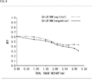
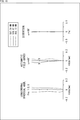
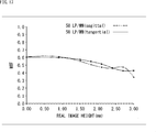
- FIG. 11 is a diagram illustrating a configuration example of an imaging lens disclosed in Patent Document 2. It is a figure which compares and shows various aberrations. It is a figure which compares and shows the image height dependence of MTF. It is a figure showing roughly an example of composition of a 2nd embodiment of an imaging lens to which this art is applied.
- FIG. 7 is a diagram illustrating lens configuration data, aspheric surface data, and configuration data of the imaging lens in FIG. 6. It is a figure which shows the various aberrations of the imaging lens of FIG.
- FIG. 11 is a diagram illustrating a configuration example of an imaging lens disclosed in Patent Document 3. It is a figure which compares and shows various aberrations. It is a figure showing roughly an example of composition of a 4th embodiment of an imaging lens to which this art is applied. It is a figure which shows the lens configuration data, aspherical surface data, and configuration data of the imaging lens of FIG. It is a figure which shows the various aberrations of the imaging lens of FIG. It is a figure which shows the image height dependence of MTF of the imaging lens of FIG. It is a block diagram which shows the structural example of an imaging device. It is a figure which shows the usage example which uses an imaging device.
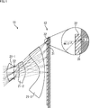
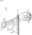
- FIG. 1 is a diagram schematically illustrating a configuration example of a first embodiment of an imaging lens to which the present technology is applied.
- the imaging lens 11 shown in FIG. 1 is mounted on various portable terminals, imaging devices such as in-vehicle cameras, mobile PCs (personal computers), wearable devices, scanners, surveillance cameras, action cams, video cameras, and digital cameras. Used.
- An imaging surface 31 of the solid-state imaging device 12 such as a CCD or a CMOS image sensor is disposed on the imaging surface of the imaging lens 11.
- various optical members such as an infrared cut filter and a low-pass filter are disposed between the image side surface of the image side lens group of the solid-state image pickup device 12 and the image pickup surface 31. May be.
- the imaging lens 11 includes a first lens 21-1, an aperture 22, a second lens 21-2, and a third lens 21- in order from the object side to the image plane side. 3 is arranged.
- the first lens 21-1 has a meniscus shape having a positive refractive index and a convex surface on the object side.
- the second lens 21-2 has a positive refractive index.
- the third lens 21-3 has a negative refractive index from the center to the periphery, and has a meniscus shape having a convex surface on the image side.
- the solid-state imaging device 12 used in combination with the imaging lens 11 has a cover glass 32 bonded directly to the imaging surface 31 formed on the semiconductor substrate (without providing a gap such as an air layer). It becomes the composition.
- the cover glass 32 is made of a material having a refractive index larger than that of air, and protects the imaging surface 31 of the solid-state imaging device 12.
- a filler (adhesive) filled between the cover glass 32 and the imaging surface 31 has a refractive index substantially equal to that of the cover glass 32.
- the light emitted from the third lens 21-3 and incident on the cover glass 32 is refracted on the surface of the cover glass 32, and is incident on the imaging surface 31 while maintaining the angle.
- the refractive index of the cover glass 32 is larger than that of air. If the imaging surface 31 can be protected, a resin other than glass may be used as the material of the cover glass 32.
- the maximum principal ray angle of emission from the imaging lens 11 can be made larger than before. .
- the maximum principal ray angle ⁇ cg incident on the cover glass 32 from the third lens 21-3 is set to satisfy 35 ° or more ( ⁇ cg> 35 °). Then, using the refractive index of the cover glass 32, the maximum chief ray incident angle on the imaging surface 31 is relaxed by 5 ° or more. For example, as shown in an enlarged view on the right side of FIG. 1, the angle ⁇ cg of the maximum principal ray incident on the cover glass 32 is set to 44.5 °, and the refractive index at the cover glass 32 is used to The maximum chief ray incident angle is relaxed to 28.3 °.
- Such a first condition is, for example, that in an imaging apparatus having a normal configuration, the maximum chief ray angle of emission from an imaging lens is generally 35 °, so that in the imaging lens 11, It is necessary to realize performance exceeding the limit.
- the image side focal length f1 of the first lens 21-1 satisfies 0.5 ⁇ f1 / f ⁇ 100 with respect to the image side focal length f of the entire optical system of the imaging lens 11, and the second condition
- the image-side focal length f2 of the second lens 21-2 satisfies 0.3 ⁇ f2 / f ⁇ 1.0
- the image-side focal length f3 of the third lens 21-3 satisfies ⁇ 1.0 ⁇ f3 / f ⁇ ⁇ 0.3.
- Such a second condition is, for example, a three-lens configuration including a first lens 21-1, an aperture 22, a second lens 21-2, and a third lens 21-3.
- 21-3 is required to realize the principal ray jumping up.
- a second lens 21-2 having a positive refractive index is arranged on the front side of the third lens 21-3 having a negative refractive index, cancels out aberrations, and forms a symmetrical shape with the diaphragm 22 interposed therebetween. This is advantageous from the viewpoint of eliminating aberrations. Therefore, the first lens 21-1 has a positive refractive index.
- the image side focal length f3 of the third lens 21-3 needs to satisfy ⁇ 1.0 ⁇ f3 / f ⁇ ⁇ 0.3.
- the second lens 21-2 required for aberration correction is too sensitive to manufacturing errors if the positive refractive index is too strong, and aberrations cannot be corrected if the refractive index is too small. Due to the positive refractive index, the image-side focal length f2 of the second lens 21-2 needs to satisfy 0.3 ⁇ f2 / f ⁇ 1.0.
- the first lens 21-1 has a symmetrical shape with the diaphragm 22 interposed therebetween, but basically, a combined configuration of the second lens 21-2 and the third lens 21-3. Therefore, the refractive index is smaller than that of the second lens 21-2. As a result, the upper limit (value is smaller) of the refractive index that the first lens 21-1 can take is determined, and the lower limit (value is the upper limit) of the refractive index can be taken until just before the negative lens is reached.
- the image-side focal length f1 of the lens 21-1 needs to satisfy 0.5 ⁇ f1 / f ⁇ 100.
- the Abbe number ⁇ cg of the cover glass 32 is set to be larger than 55 ( ⁇ cg> 55).
- the third condition is that, for example, when the Abbe number of the cover glass 32 is smaller than 55, the refractive index dispersion due to the wavelength increases, and therefore, an extra aberration occurs due to a synergistic effect with a large incident angle. Resulting in. As a result, the third condition is required in order to suppress the deterioration of MTF (Modulation Transfer Function: optical transfer function).
- MTF Modulation Transfer Function: optical transfer function
- the thickness Tcg of the cover glass 32 is set to be 0.3 mm or less (Tcg ⁇ 0.3 mm).
- Such a fourth condition is because, for example, various types of portable terminal cameras and in-vehicle cameras are required to be miniaturized, and the cover glass 32 is required to be thin. For example, in order to satisfy the recent required resolution, there is a concern that the aberration generated by the thick cover glass 32 affects the MTF. Therefore, the fourth condition is necessary as an allowable limit for affecting the MTF.
- the back focus Bf from the cover glass 32 to the imaging lens 11 is set to be 0.2 mm or less (Bf ⁇ 0.2 mm).
- a bright F value is required as a recent trend, and in order to realize a bright F value, the angle between the upper ray and the lower ray of an imaged ray is steep.
- the fifth condition is necessary because the back focus is also limited.
- the imaging lens 11 and the solid-state imaging device 12 having these first to fifth conditions are optimized so as to have more favorable imaging performance, for example, the maximum chief ray angle is expanded and more compact.
- a simple optical system can be realized.
- FIG. 2 shows specific examples of numerical values of the lens configuration data, aspherical data, and configuration data of the imaging lens 11.
- the imaging lens 11 is a CMOS image sensor used in an imaging device mounted on a small mobile device such as a so-called smartphone, for example, 1/4 size, 2.2 ⁇ m pixel pitch, 2 million. Specific numerical values when applied to a pixel CMOS image sensor are shown.
- the aspherical data shown in FIG. 2 indicates that the distance from the tangential plane of the aspherical vertex of the coordinate point on the aspherical surface where the height from the optical axis is y is X, and the curvature of the aspherical vertex (1 / r ) Is used in the following formula (1) representing the aspherical surfaces of the first lens 21-1, the second lens 21-2, and the third lens 21-3.
- FIG. 3 shows a configuration example of an imaging lens having a configuration based on the disclosure in Patent Document 2 described above.
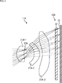
- the imaging lens 11A includes a first lens 21A-1, an aperture 22A, a second lens 21A-2, and a third lens 21A- in order from the object side to the image plane side. 3 is arranged, and is assumed to be used in combination with the solid-state imaging device 12A in which a gap is provided between the imaging surface 31 and the cover glass 32.
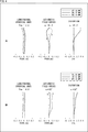
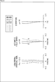
- FIGS. 4A and FIG. 5A show various aberrations of the imaging lens 11 and the image height dependency of MTF.
- FIG. 4B and FIG. 5B show various aberrations of the imaging lens 11A and The image height dependence of MTF is shown.
- the imaging lens 11 and the imaging lens 11 ⁇ / b> A are designed under the same constraint conditions.
- the imaging lens 11A having a configuration based on the disclosure in Patent Document 2 described above has an optical total length of 3.7 mm, suppresses the maximum principal ray incident angle on the imaging surface 31 to 27 °, and realizes a half angle of view of 32 °. Yes. Furthermore, the imaging lens 11A is a white light MTF with a frequency of 110 lps / mm, which is approximately half the Nyquist frequency of 2.2 ⁇ m pixel pitch, and realizes 46.7% on the axis and 45.0% for sagittal and 46.6% for sagittal at 70% increase. .
- the increase in 90% is 27.9% for meridional and 41.3% in sagittal, and the increase in 10% is 17.6% for meridional and 34.7% in sagittal.
- the third lens 21A-3 has a negative action at the center and a positive action at the periphery, and therefore when the aberration is canceled at the center, the aberration cannot be canceled at the periphery.
- it is balanced to some extent, and some aberrations remain not only at the periphery but also at the center. Therefore, it can be realized only with an F value of 4 and a half angle of view up to 32 °.
- the chief ray angle of lens emission at a height of 10% is 45.5 °, and it is refracted on the surface of the cover glass 32 and bent to 28.3 °.
- the principal ray angle of the lens emission is the largest at 47.3 ° at 90% increase, and is refracted on the surface of the cover glass 32 and bent to 29.3 °, so that the incident angle to the imaging surface 31 becomes desirable.
- the imaging lens 11 can achieve a wide angle of 41.3 ° with a bright lens having an F value of 2.8 while keeping the optical total length as short as 2.9 mm in a 1/4 size sensor. Furthermore, the imaging lens 11 has a white light MTF with a frequency of 110 lps / mm, which is approximately half of the Nyquist frequency of 2.2 ⁇ m pixel pitch, 54.4% on the axis, 70% higher at merital 44.0% and sagittal 39.7%, at 90% higher merit-onal. With 28.3% and sagittal 42.4%, an increase of 10% can achieve 25.3% of merital and 26.9% of sagittal.
- the imaging lens 11 is 22% shorter in optical total length than the imaging lens 11A, is 30% brighter, and can sufficiently secure the MTF of the peripheral image height. This is because the imaging lens 11 is a negative lens in which the third lens 21-3 does not have a wave shape, and aberrations are eliminated with a positive / negative configuration as a whole, and the principal ray angle of the lens exit is allowed up to 47.3 °. This can be realized by increasing the degree of freedom in design and using the refraction of the cover glass 32 to relax the light incident angle desired for the imaging surface 31 to optimize the entire apparatus.
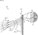
- FIG. 6 is a diagram schematically illustrating a configuration example of the second embodiment of the imaging lens to which the present technology is applied. Also, the solid-state imaging device 12 shown in FIG. 6 has a configuration in which a cover glass 32 is directly joined to the imaging surface 31 as in FIG. 1, and detailed description thereof is omitted.
- the imaging lens 11B includes a first lens 21B-1, an aperture 22B, a second lens 21B-2, and a third lens 21B- in order from the object side to the image plane side. 3 is arranged.
- the first lens 21B-1 is a spherical glass having a positive refractive index and a meniscus shape having a convex surface on the object side.
- the second lens 21B-2 is an aspheric glass having a positive refractive index.
- the third lens 21B-3 is a spherical glass having a negative refractive index and a meniscus shape having a convex surface on the image side.
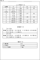
- FIG. 7 shows specific examples of numerical values of the lens configuration data, aspheric surface data, and configuration data of the imaging lens 11B. 8 shows various aberrations of the imaging lens 11B, and FIG. 9 shows the image height dependency of the MTF of the imaging lens 11B.
- the imaging lens 11B is applied to a CMOS image sensor used in an imaging apparatus for in-vehicle use, for example, a 1/3 size CMOS image sensor having a 3.0 ⁇ m pixel pitch and 2 million pixels. The specific numerical value is shown.
- the imaging lens 11B is increased by 10% and the principal ray angle of lens emission is 54.2 °, and is refracted on the surface of the cover glass 32 and bent to 32.7 °.
- the desired incident angle on the surface 31 is obtained.
- the replacement of the rearview mirror of the vehicle with a camera is optimal for the entire angle of view around 60 °, and this angle of view is obtained by a horizontal image in a sensor having an aspect ratio of 4: 3 effective pixels.
- the angle is 60 °.
- the replacement of the vehicle rearview mirror with a camera requires that there is no performance degradation at ambient temperature and that flare can be sufficiently suppressed.
- the imaging lens 11B avoids performance degradation at ambient temperature by employing glass lenses for all of the first lens 21B-1, the second lens 21B-2, and the third lens 21B-3. can do. Furthermore, since the glass lens can be coated with low reflection, the imaging lens 11B has a configuration capable of suppressing flare.
- the imaging lens 11B has a troublesome glass mold lens as one of the second lenses 21B-2, and the first lens 21B-1 and the third lens 21B-3. It is considered to be composed of spherical lenses that can be produced stably without fatal trouble.
- the imaging lens 11B eliminates aberration with a positive / negative configuration as a whole, allows the principal ray angle of the lens exit to 54.2 °, increases the degree of design freedom, and utilizes the refraction of the cover glass 32. This can be realized by relaxing the light incident angle desired on the imaging surface 31 and optimizing the entire apparatus.
- FIG. 10 is a diagram schematically illustrating a configuration example of the third embodiment of the imaging lens to which the present technology is applied. Further, the solid-state imaging device 12 shown in FIG. 10 has a configuration in which a cover glass 32 is directly joined to the imaging surface 31 as in FIG. 1, and detailed description thereof is omitted.
- the imaging lens 11C has a first lens 21C-1, an aperture 22C, a second lens 21C-2, and a third lens 21C- in order from the object side to the image plane side. 3 is arranged.
- the first lens 21C-1 is a spherical glass having a positive refractive index and a meniscus shape having a convex surface on the object side.
- the second lens 21B-2 is an aspheric glass having a positive refractive index.
- the third lens 21B-3 is an aspheric lens having a negative refractive index from the center to the periphery.
- the object side surface is bent uniformly toward the object side as it goes to the periphery, while the image side is bent uniformly from the center to the middle side toward the image side.
- it has a curved and wavy shape, but as a lens effect, it acts negatively uniformly from the center to the periphery.
- FIG. 11 shows specific examples of numerical values of the lens configuration data, aspherical data, and configuration data of the imaging lens 11C.
- FIG. 11 shows a case where the imaging lens 11C is applied to a CMOS image sensor used in a vehicle-mounted imaging device, for example, a 1/4 size, VGA (Video Graphics Array) standard CMOS image sensor. Specific numerical values are shown.
- the light emitted from the imaging lens 11C is enlarged by 10% and has a principal ray angle of 53.6 °, which is 53.6 °, which is refracted on the surface of the cover glass 32, as shown on the right side of FIG. To obtain a desired incident angle on the imaging surface 31.
- FIG. 12 shows a configuration example of an imaging lens having a configuration based on the disclosure in Patent Document 3 described above.
- the imaging lens 11D has a first lens 21D-1, a second lens 21D-2, an aperture 22D, and a third lens 21D- in order from the object side to the image plane side. 3 is used, and is assumed to be used in combination with a solid-state imaging device 12D in which a gap is provided between the imaging surface 31 and the cover glass 32.
- FIG. 13A shows various aberrations of the imaging lens 11C
- FIG. 13B shows various aberrations of the imaging lens 11D.
- the imaging lens 11C and the imaging lens 11D are designed under the same constraint conditions.
- the imaging lens 11C and the imaging lens 11D are designed as an in-vehicle camera module (genre called 90 ° camera) having a three-piece CMOS image sensor used in an imaging apparatus for in-vehicle use. Specific numerical values when applied to a CMOS image sensor of 4 sizes and VGA standards are shown.
- the imaging lens 11D based on the disclosure in Patent Document 3 described above includes, in order from the object side, a first lens 21D-1 of a low-dispersion glass material having a negative refractive index, and a high-dispersion glass material having a positive refractive index.
- a second lens 21D-2, a stop 22D, and a third lens 21D-3 made of a glass material having a positive refractive index and low dispersion are configured.
- the imaging lens 11D realizes a focal length of 2.32 mm, an F value of 2.8, and an optical total length of 13.2 mm.
- the imaging lens 11D has a configuration in which the second lens 21D-2 is achromatic by using a high-dispersion glass material having a positive refractive index.
- a negative lens uses high-dispersion. The effect of achromatization becomes higher. For this reason, the imaging lens 11D has a low aberration suppression effect as a whole structure, so that the optical length is long and the F value is only 2.8.
- the imaging lens 11C shown in FIG. 10 can realize a bright lens with an F value of 2.0 while keeping the optical total length as short as 4.14 mm in a 1/4 size 90 ° camera.
- the imaging lens 11C has an optical total length of 1/3 or less and an F value that is 40% brighter than the imaging lens 11D.
- the imaging lens 11C is astigmatism while suppressing distortion. Aberration and spherical aberration can be reduced.
- the imaging lens 11C eliminates aberration with positive and negative configurations, allows the principal ray angle of the lens exit to 53.6 °, increases the degree of design freedom, and uses the refraction of the cover glass 32 to capture the imaging surface 31. This can be realized by relaxing the beam incident angle to a desired value and optimizing the entire apparatus.
- FIG. 14 is a diagram schematically illustrating a configuration example of a fourth embodiment of an imaging lens to which the present technology is applied. Further, the solid-state imaging device 12 shown in FIG. 14 has a configuration in which a cover glass 32 is directly joined to the imaging surface 31 as in FIG. 1, and detailed description thereof is omitted.
- the imaging lens 11E includes a first lens 21E-1, an aperture 22E, a second lens 21E-2, and a third lens 21E- in order from the object side to the image plane side. 3 is arranged.
- the first lens 21E-1 is an aspheric glass having a positive refractive index and a meniscus shape having a convex surface on the object side.
- the second lens 21E-2 is a spherical glass having a positive refractive index.
- the third lens 21E-3 is a spherical lens having a negative refractive index and a meniscus shape having a convex surface on the image side.
- FIG. 15 shows specific examples of numerical values of the lens configuration data, aspheric surface data, and configuration data of the imaging lens 11E.
- 16 shows various aberrations of the imaging lens 11E
- FIG. 17 shows the image height dependence of the MTF of the imaging lens 11E.
- the imaging lens 11E is applied to a CMOS image sensor used in an in-vehicle imaging device, for example, a 1/3 size, 3.0 ⁇ m pixel pitch, 2 million pixel CMOS image sensor.
- the specific numerical value is shown.
- the light emitted from the imaging lens 11E is enlarged by 10%, the principal ray angle of the lens exit is 51.0 °, and is refracted at the surface of the cover glass 32 and bent to 31.1 °, as shown on the right side of FIG. As a result, the incident angle on the image pickup surface 31 is desirable. As a result, a 1/3 size sensor with 2 million pixels realizes a wide angle of 33 ° with a bright lens with F value of 2.0 while keeping the optical total length as short as 7.5mm.
- the replacement of the vehicle rearview mirror with a camera is optimal when the total angle of view is around 60 °, and this angle of view is FullHD (High Definition) with an effective pixel aspect ratio of about 2: 1. ) In the standard sensor, the horizontal angle of view is 60 °. Furthermore, the replacement of the vehicle rearview mirror with a camera requires that there is no performance degradation at ambient temperature and that flare can be sufficiently suppressed.
- the imaging lens 11E employs glass lenses for all of the first lens 21E-1, the second lens 21E-2, and the third lens 21E-3, thereby avoiding performance degradation at ambient temperature. can do. Furthermore, since the glass lens can be coated with low reflection, the imaging lens 11E is configured to suppress flare.
- the imaging lens 11E has a trouble-free glass mold lens as one of the first lenses 21E-1, and the second lens 21E-2 and the third lens 21E-3. It is considered to be composed of spherical lenses that can be produced stably without fatal trouble.
- the imaging lens 11E eliminates aberration with a positive / negative configuration as a whole, allows the principal ray angle of the lens emission to be 51.0 °, increases the degree of design freedom, and utilizes the refraction of the cover glass 32. This can be realized by relaxing the light incident angle desired on the imaging surface 31 and optimizing the entire apparatus.
- the imaging lens 11 relaxes the incident angle on the imaging surface 31 by refraction by the cover glass 32.
- a lens having a steeper incident angle of the maximum principal ray from the imaging lens 11 to the cover glass 32 can be used.
- the imaging lens 11 is the most suitable configuration in an imaging device that employs a three-lens configuration.
- the light beam angle of the lens exit and the incident angle to the image sensor are equal, and the limit of the incident angle of the image sensor is the light beam angle limit of the lens exit.
- the limit of the incident angle of the image sensor is the light beam angle limit of the lens exit.
- the electronic imaging device since the distance between the photoelectric conversion portion of each element and the color filter that separates colors is separated, light entering from an angle may enter a different element from the element that has passed the color filter. As a result, false colors may be generated.
- the electronic imaging device has an incident angle limitation because the efficiency of incident light is deteriorated by the action of the structure and the optical thin film constituting the structure.
- the most image side lens has a concave action at the center and a convex action at the periphery to obtain an optimal solution.
- the center has a concave action and the periphery has a convex action
- aberration correction is not compatible between the center and the periphery, and the overall characteristics such as the optical total length, the angle of view, and the F value are This aberration was rate limiting.
- the imaging lens 11 of the present embodiment is a three-lens camera module and is combined with the solid-state imaging device 12 in which the cover glass 32 is attached to the imaging surface 31 without providing an air gap. used.
- the imaging lens 11 has a positive and negative power arrangement that is advantageous from the viewpoint of aberration correction, and the third lens 21-3 on the most image side is negative from the center to the periphery. High performance can be realized by using a shape with the above action.
- the imaging lens 11 of the present embodiment a configuration example has been shown in which an optical total length of 2.9 mm is realized with a 1/4 size. Further, the emission angle of the maximum principal ray from the imaging lens 11 is set to 47 ° or more, aberration correction becomes easy, and an unprecedented low profile can be realized.
- the imaging lens 11 of the present embodiment is suitable for use in an in-vehicle imaging device.
- an in-vehicle camera having a total angle of view of about 50 ° to 90 ° often employs a three-lens configuration.
- the imaging lens 11 according to the present embodiment allows a higher principal ray angle than ever before to increase the degree of design freedom, eliminates aberrations with positive and negative structures, and covers glass.
- the refraction of 32 is used to relax the light incident angle desired for the imaging surface 31.
- the imaging lens 11 of this Embodiment became a suitable structure for applying to the vehicle-mounted lens of 3 glass composition.
- the imaging lens 11 of the present embodiment can be configured to use only one glass mold lens having many troubles and two spherical lenses that can be stably produced. Therefore, from the viewpoint of productivity, the imaging lens 11 according to the present embodiment can introduce the glass configuration to all the lenses with confidence.
- the imaging lens 11 and the solid-state imaging device 12 as described above are various electronic devices such as an imaging system such as a digital still camera and a digital video camera, a mobile phone having an imaging function, or other equipment having an imaging function. It can be applied to equipment.
- FIG. 18 is a block diagram illustrating a configuration example of an imaging device mounted on an electronic device.
- the imaging apparatus 101 includes an optical system 102, an imaging element 103, a signal processing circuit 104, a monitor 105, and a memory 106, and can capture still images and moving images.
- the above-described imaging lens 11 is applied to the optical system 102, guides image light (incident light) from the subject to the imaging element 103, and forms an image on the light receiving surface (sensor unit) of the imaging element 103.
- the solid-state image sensor 12 described above is applied.
- the image sensor 103 electrons are accumulated for a certain period according to an image formed on the light receiving surface via the optical system 102. Then, a signal corresponding to the electrons accumulated in the image sensor 103 is supplied to the signal processing circuit 104.
- the signal processing circuit 104 performs various signal processing on the pixel signal output from the image sensor 103.
- An image (image data) obtained by performing signal processing by the signal processing circuit 104 is supplied to the monitor 105 and displayed, or supplied to the memory 106 and stored (recorded).
- a higher quality image can be taken by applying the imaging lens 11 and the solid-state imaging device 12 described above.
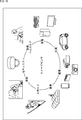
- FIG. 19 is a diagram illustrating a usage example in which the above-described image sensor (camera module including the imaging lens 11 and the solid-state imaging device 12) is used.
- the image sensor described above can be used in various cases for sensing light such as visible light, infrared light, ultraviolet light, and X-ray as follows.
- Devices for taking images for viewing such as digital cameras and mobile devices with camera functions
- Devices used for traffic such as in-vehicle sensors that capture the back, surroundings, and interiors of vehicles, surveillance cameras that monitor traveling vehicles and roads, and ranging sensors that measure distances between vehicles, etc.
- Equipment used for home appliances such as TVs, refrigerators, air conditioners, etc. to take pictures and operate the equipment according to the gestures ⁇ Endoscopes, equipment that performs blood vessel photography by receiving infrared light, etc.
- Equipment used for medical and health care ⁇ Security equipment such as security surveillance cameras and personal authentication cameras ⁇ Skin measuring instrument for photographing skin and scalp photography Such as a microscope to do beauty Equipment used for sports-Equipment used for sports such as action cameras and wearable cameras for sports applications-Used for agriculture such as cameras for monitoring the condition of fields and crops apparatus
- this technique can also take the following structures.
- a first lens, a second lens, and a third lens are arranged from the object side to the image side.
- a cover member made of a medium having a refractive index higher than that of air is bonded directly on the imaging surface of the image sensor, and a maximum principal ray incident on the cover member from the third lens exceeds 35 °, and
- the first lens has a positive refractive power;
- the second lens has a positive refractive power;
- the third lens has negative refractive power;
- (1) 0.5 ⁇ f1 / f ⁇ 100 (2) 0.3 ⁇ f2 / f ⁇ 1.0 (3) -1.0 ⁇ f3 / f ⁇ ⁇ 0.3
- f Image side focal length f1 of the entire optical system
- f1 Image side focal length f2 of the first lens
- f2 Image side focal length f3 of the second lens
- f3 Image side focal length of the third lens.
- An imaging lens configured by arranging a first lens, a second lens, and a third lens from the object side toward the image side;
- An imaging element in which a cover member made of a medium having a refractive index higher than air is joined directly on the imaging surface, The maximum chief ray incident on the cover member from the third lens exceeds 35 °, and the maximum chief ray incident angle on the imaging surface is relaxed by 5 ° or more using the refractive index of the cover member.
Landscapes
- Physics & Mathematics (AREA)
- General Physics & Mathematics (AREA)
- Optics & Photonics (AREA)
- Lenses (AREA)
Abstract
本開示は、より最適化を図ることができるようにする撮像レンズおよび撮像装置に関する。 撮像レンズは、物体側から像側に向かって、第1のレンズ、第2のレンズ、および第3のレンズが配置されて構成される。撮像素子は、撮像面上に直接的に、空気より屈折率の高い媒質からなるカバー部材が接合されている。そして、第3のレンズからカバー部材に入射する最大主光線が35°を超え、かつ、カバー部材での屈折率を利用して撮像面への最大主光線入射角が5°以上緩和される。本技術は、例えば、小型化が求められる撮像装置に適用できる。
Description
本開示は、撮像レンズおよび撮像装置に関し、特に、より最適化を図ることができるようにした撮像レンズおよび撮像装置に関する。
従来、CCD(Charge Coupled Device)やCMOS(Complementary Metal Oxide Semiconductor)イメージセンサなどの固体撮像素子で使用される撮像レンズとして、様々な特性を備えた撮像レンズが開発されている。
例えば、特許文献1には、物体側から順に、正の屈折力を有する第1のレンズ、絞り、正の屈折力を有する第2のレンズ、負の屈折力を有する第3のレンズが配置され、特許文献1に記載の各条件を満足する撮像レンズが開示されている。
また、特許文献2には、物体側から順に、正のパワーを有する第1のレンズ、絞り、正のパワーを有する第2のレンズ、中心部で負のパワーを有し、周辺部で正のパワーを有する第3のレンズが配置され、特許文献2に記載の第1乃至第3の条件式を満足する撮像レンズが開示されている。
また、特許文献3には、物体側から順に、凹非球面レンズである第1のレンズ、凸非球面レンズである第2のレンズ、および、凸非球面レンズである第3のレンズが配置され、特許文献3に記載の第1乃至第3の条件式を満足する広角レンズが開示されている。
ところで、従来、上述の特許文献1乃至3で開示されているような撮像レンズが開発されているが、例えば、撮像面上に直接的にカバー部材が接合された撮像素子との組み合わせで最適化が図られた撮像レンズが求められている。
本開示は、このような状況に鑑みてなされたものであり、より最適化を図ることができるようにするものである。
本開示の一側面の撮像レンズは、物体側から像側に向かって、第1のレンズ、第2のレンズ、および第3のレンズが配置されて構成され、撮像素子の撮像面上に直接的に、空気より屈折率の高い媒質からなるカバー部材が接合されており、前記第3のレンズから前記カバー部材に入射する最大主光線が35°を超え、かつ、前記カバー部材での屈折率を利用して前記撮像面への最大主光線入射角が5°以上緩和される。
本開示の一側面の撮像装置は、物体側から像側に向かって、第1のレンズ、第2のレンズ、および第3のレンズが配置されて構成される撮像レンズと、撮像面上に直接的に、空気より屈折率の高い媒質からなるカバー部材が接合されている撮像素子とを備え、前記第3のレンズから前記カバー部材に入射する最大主光線が35°を超え、かつ、前記カバー部材での屈折率を利用して前記撮像面への最大主光線入射角が5°以上緩和される。
本開示の一側面においては、撮像レンズは、物体側から像側に向かって、第1のレンズ、第2のレンズ、および第3のレンズが配置されて構成され、撮像素子は、撮像面上に直接的に、空気より屈折率の高い媒質からなるカバー部材が接合されている。そして、第3のレンズからカバー部材に入射する最大主光線が35°を超え、かつ、カバー部材での屈折率を利用して撮像面への最大主光線入射角が5°以上緩和される。
本開示の一側面によれば、より最適化を図ることができる。
なお、ここに記載された効果は必ずしも限定されるものではなく、本開示中に記載されたいずれかの効果であってもよい。
以下、本技術を適用した具体的な実施の形態について、図面を参照しながら詳細に説明する。
<撮像レンズの第1の構成例>
図1は、本技術を適用した撮像レンズの第1の実施の形態の構成例を概略的に示す図である。
図1は、本技術を適用した撮像レンズの第1の実施の形態の構成例を概略的に示す図である。
例えば、図1に示す撮像レンズ11は、各種の携帯端末や、車載カメラ、モバイルPC(Personal Computer)、ウェアラブル機器、スキャナ、監視カメラ、アクションカム、ビデオカメラ、ディジタルカメラなどの撮像装置に搭載して使用される。また、撮像レンズ11の結像面には、CCDやCMOSイメージセンサなどの固体撮像素子12の撮像面31が配置される。さらに、固体撮像素子12の像側レンズ群の像側面と撮像面31との間には、カバーガラス32の他、赤外カットフィルタやローパスフィルタなどの各種の光学部材(図示せず)が配置されていてもよい。
図1に示すように、撮像レンズ11は、物体側から像面側に向かって順番に、第1のレンズ21-1、絞り22、第2のレンズ21-2、および第3のレンズ21-3が配置されて構成される。第1のレンズ21-1は、正の屈折率を有して物体側に凸面を有するメニスカス形状をなす。第2のレンズ21-2は、正の屈折率を有する。第3のレンズ21-3は、中心から周辺に至るまで負の屈折率を有し、像側に凸面を有するメニスカス形状をなす。
撮像レンズ11と組み合わされて使用される固体撮像素子12は、半導体基板に形成される撮像面31に対して直接的に(空気層などの隙間が設けられることなく)、カバーガラス32が接合された構成となっている。カバーガラス32は、空気より屈折率が大きな材質により構成され、固体撮像素子12の撮像面31を保護する。また、カバーガラス32と撮像面31との間に充填される充填剤(接着剤)も、カバーガラス32とほぼ等しい屈折率のものが用いられる。
従って、第3のレンズ21-3から射出されてカバーガラス32に入射する光は、カバーガラス32の表面で屈折し、ほぼその角度を維持して、撮像面31に入射することになる。ここで、カバーガラス32による屈折の効果を得ることを目的として、カバーガラス32の屈折率は空気より大きい方が好適である。なお、撮像面31を保護することができれば、カバーガラス32の材質として、ガラス以外の樹脂などを用いてもよい。
このような撮像レンズ11および固体撮像素子12を組み合わせて用い、以下で説明するような条件を備えることで、撮像レンズ11の出射の最大主光線角度を、従来よりも大きくすることが可能となる。
まず、撮像レンズ11および固体撮像素子12が備える第1の条件として、第3のレンズ21-3からカバーガラス32へ入射する最大主光線の角度θcgが35°以上を満たすように設定(θcg>35°)される。そして、カバーガラス32での屈折率を利用して、撮像面31への最大主光線入射角を5°以上緩和される。例えば、図1の右側に拡大して示すように、カバーガラス32へ入射する最大主光線の角度θcgは44.5°に設定され、カバーガラス32での屈折率を利用して、撮像面31への最大主光線入射角が28.3°に緩和されている。
このような第1の条件は、例えば、通常の構成の撮像装置では、撮像レンズ出射の最大主光線角度が35°であることが一般的な限界であることより、撮像レンズ11において、そのような限界を超える性能を実現するために必要となる。
第2の条件として、撮像レンズ11の光学系全体の像側焦点距離fに対して、第1のレンズ21-1の像側焦点距離f1が、0.5≦f1/f≦100を満たし、第2のレンズ21-2の像側焦点距離f2が、0.3≦f2/f≦1.0を満たし、第3のレンズ21-3の像側焦点距離f3が、-1.0≦f3/f≦-0.3を満たすように設定される。
このような第2の条件は、例えば、第1のレンズ21-1、絞り22、第2のレンズ21-2、および第3のレンズ21-3の3枚構成で、最終の第3のレンズ21-3が、主光線を跳ね上げることを実現するために必要となる。例えば、負の屈折率を有する第3のレンズ21-3の前側に正の屈折率の第2のレンズ21-2が配置され、収差を打消し、さらに絞り22を挟んで、対称形を形成する方が収差を消す観点から有利となる。そのため、第1のレンズ21-1が正の屈折率となる。
まず、カバーガラス32に入射する最大主光線が35°以上であるために、第3のレンズ21-3の像側焦点距離f3が、-1.0≦f3/f≦-0.3を満たす必要がある。そして、その収差補正に必要な第2のレンズ21-2は、正の屈折率が強すぎると、製造誤差に敏感になりすぎ、屈折率が小さすぎると収差を補正することができなくなる。その正の屈折率のために、第2のレンズ21-2の像側焦点距離f2が、0.3≦f2/f≦1.0を満たす必要がある。
さらに、第1のレンズ21-1は、絞り22を挟んで、対称形になるのが望ましいが、基本的に、第2のレンズ21-2および第3のレンズ21-3の合成された構成と相対することになるので、屈折率は、第2のレンズ21-2より小さくなる。それによって、第1のレンズ21-1が取り得る屈折率の上限(値は小さい方)が決まり、屈折率の下限(値は上限)は、負のレンズになる直前まで取り得るので、第1のレンズ21-1の像側焦点距離f1が、0.5≦f1/f≦100を満たす必要がある。
第3の条件として、カバーガラス32のアッベ数νcgが55より大きくなるように設定(νcg>55)される。
このような第3の条件は、例えば、カバーガラス32のアッベ数が55より小さくなると、波長による屈折率分散が大きくなるため、入射角が大きく入ることとの相乗効果で、余分な収差が発生してしまう。これにより、MTF(Modulation Transfer Function:光学伝達関数)が劣化してしまうのを抑制するために、第3の条件が必要となる。
第4の条件として、カバーガラス32の厚みTcgが0.3mm以下となるように設定(Tcg≦0.3mm)される。
このような第4の条件は、例えば、各種の携帯端末用のカメラや車載カメラなどでは小型化が求められており、カバーガラス32を薄くすることが要求されていることによる。例えば、近年の要求解像度を満たすためには、カバーガラス32が厚いことによって発生する収差がMTFに影響を及ぼすことが懸念される。従って、MTFに影響を及ぼすことに対する許容限界として、第4の条件が必要となる。
第5の条件として、カバーガラス32から撮像レンズ11までのバックフォーカスBfが、0.2mm以下となるように設定(Bf≦0.2mm)される。
このような第5の条件は、例えば、近年の傾向として明るいF値が要求されており、明るいF値を実現するためには、結像する光線の上光線と下光線の角度が急峻である必要がある。例えば、仮にバックフォーカスが長い構成では、少なくとも最終レンズの有効径が大きくなる必要があるのに対し、各種の携帯端末用のカメラや車載カメラなどでは小型化が求められていて相反することになる。従って、バックフォーカスにも制限が設けられることより、第5の条件が必要となる。
これらの第1乃至第5の条件を備える撮像レンズ11および固体撮像素子12は、より好ましい結像性能となるように最適化が図られ、例えば、最大主光線角度を拡大し、かつ、よりコンパクトな光学系を実現することができる。
図2には、撮像レンズ11のレンズ構成データ、非球面データ、および構成データの数値の具体的な一例が示されている。ここで、図2には、撮像レンズ11を、いわゆるスマートフォンなどのような小型のモバイル機器に搭載される撮像装置で用いられるCMOSイメージセンサ、例えば、1/4サイズ、2.2μmピクセルピッチ、200万画素のCMOSイメージセンサに対して適用したときの具体的な数値が示されている。
また、図2に示す非球面データは、光軸からの高さがyとなる非球面上の座標点の非球面頂点の接平面からの距離をXとし、非球面頂点の曲率(1/r)をcとして、第1のレンズ21-1、第2のレンズ21-2、および第3のレンズ21-3の非球面を表す次の式(1)において用いられる。

ここで、撮像レンズ11と比較するために、図3には、上述した特許文献2における開示に基づいた構成の撮像レンズの構成例が示されている。
図3に示すように、撮像レンズ11Aは、物体側から像面側に向かって順番に、第1のレンズ21A-1、絞り22A、第2のレンズ21A-2、および第3のレンズ21A-3が配置され、撮像面31とカバーガラス32との間に隙間が設けられている固体撮像素子12Aと組み合わされて使用されることが想定されている。
図4を参照して、撮像レンズ11および撮像レンズ11Aの諸収差について説明し、図5を参照して、撮像レンズ11および撮像レンズ11AのMTFの像高依存性について説明する。
図4のAおよび図5のAには、撮像レンズ11の諸収差およびMTFの像高依存性が示されており、図4のBおよび図5のBには、撮像レンズ11Aの諸収差およびMTFの像高依存性が示されている。なお、図4および図5において比較を行うために、撮像レンズ11および撮像レンズ11Aは、同様の制約条件で設計されている。
例えば、上述した特許文献2における開示に基づいた構成の撮像レンズ11Aは、光学全長が3.7mmで、撮像面31に対する最大主光線入射角度を27°に抑え、半画角32°を実現している。さらに、撮像レンズ11Aは、2.2μmピクセルピッチのナイキスト周波数のおおよそ半分の周波数110lps/mmの白色光のMTFで、軸上46.7%、7割増高でメリヂオナル45.0%およびサジタル46.6%を実現している。
しかしながら、撮像レンズ11Aでは、9割増高でメリヂオナル27.9%およびサジタル41.3%となり、10割増高でメリヂオナル17.6%およびサジタル34.7%となって、周辺像高でMTFが劣化する。それは、第3のレンズ21A-3が中心で負の作用をし、周辺で正の作用をするため、中心で収差を打ち消した場合には、周辺で収差が打ち消せないためである。実際は、ある程度バランスされており、周辺だけでなく、中心でも若干の収差が残る。そのためF値4で半画角も32°までしか実現することができない。
これに対し、図1に示す撮像レンズ11では、10割増高におけるレンズ出射の主光線角度が45.5°で、カバーガラス32の表面で屈折して28.3°に曲げられる。また、撮像レンズ11では、9割増高においてレンズ出射の主光線角度が一番大きく47.3°となり、カバーガラス32の表面で屈折して29.3°に曲げられ、撮像面31に望ましい入射角度になる。
これらにより、撮像レンズ11は、1/4サイズのセンサにおいて、光学全長が2.9mmと短く抑えながら、F値2.8という明るいレンズで、半画角41.3°という広角を実現することができる。さらに、撮像レンズ11は、2.2μmピクセルピッチのナイキスト周波数のおおよそ半分の周波数110lps/mmの白色光のMTFで軸上54.4%、7割増高でメリヂオナル44.0%およびサジタル39.7%、9割増高でメリヂオナル28.3%およびサジタル42.4%、10割増高でメリヂオナル25.3%およびサジタル26.9%を実現することができる。
従って、撮像レンズ11は、撮像レンズ11Aと比較して、光学全長が22%短くなり、30%も明るく、かつ、周辺像高のMTFも十分確保することができる。これは、撮像レンズ11が、第3のレンズ21-3が形状にうねりを持たない負のレンズで、全体として正正負の構成で収差を消して、レンズ射出の主光線角度を47.3°まで許容し、設計自由度を上げ、カバーガラス32の屈折を利用して撮像面31に望ましい光線入射角度に緩和して、装置全体として最適化が図られることで実現することができる。
<撮像レンズの第2の構成例>
図6は、本技術を適用した撮像レンズの第2の実施の形態の構成例を概略的に示す図である。また、図6に示す固体撮像素子12は、図1と同様に、撮像面31に対して直接的に、カバーガラス32が接合された構成となっており、その詳細な説明は省略する。
図6は、本技術を適用した撮像レンズの第2の実施の形態の構成例を概略的に示す図である。また、図6に示す固体撮像素子12は、図1と同様に、撮像面31に対して直接的に、カバーガラス32が接合された構成となっており、その詳細な説明は省略する。
図6に示すように、撮像レンズ11Bは、物体側から像面側に向かって順番に、第1のレンズ21B-1、絞り22B、第2のレンズ21B-2、および第3のレンズ21B-3が配置されて構成される。第1のレンズ21B-1は、正の屈折率を有して物体側に凸面を有するメニスカス形状をなす球面ガラスである。第2のレンズ21B-2は、正の屈折率を有する非球面ガラスである。第3のレンズ21B-3は、負の屈折率を有し、像側に凸面を有するメニスカス形状をなす球面ガラスである。
また、図7には、撮像レンズ11Bのレンズ構成データ、非球面データ、および構成データの数値の具体的な一例が示されている。また、図8には、撮像レンズ11Bの諸収差が示さており、図9には、撮像レンズ11BのMTFの像高依存性が示されている。なお、図7乃至図9には、撮像レンズ11Bを、車載用途の撮像装置で用いられるCMOSイメージセンサ、例えば、1/3サイズ、3.0μmピクセルピッチ、200万画素のCMOSイメージセンサに対して適用したときの具体的な数値が示されている。
そして、撮像レンズ11Bは、図6の右側に拡大して示すように、10割増高でレンズ出射の主光線角度が54.2°となり、カバーガラス32の表面で屈折して32.7°に曲げられ、撮像面31に望ましい入射角度になる。これらにより、1/3サイズの200万画素のCMOSイメージセンサにおいて、光学全長が6.2mmと短く抑えながら、F値2.0という明るさで、半画角37°という広角を実現することができる。
ところで、車両のバックミラーのカメラによる置き換えは、全画角が60°近辺であることが最適と言われており、この画角は、有効画素の縦横比が4:3のセンサにおいて、水平画角が60°になる構成である。さらに、車両のバックミラーのカメラによる置き換えは、環境温度での性能劣化が無いことと、フレアを十分抑制できていることが必要となる。
そこで、撮像レンズ11Bは、第1のレンズ21B-1、第2のレンズ21B-2、および第3のレンズ21B-3の全てにガラスレンズを採用することで、環境温度での性能劣化を回避することができる。さらに、ガラスレンズは、低反射のコーティングができるため、撮像レンズ11Bは、フレアを抑制できる構成となっている。
また、生産性の観点でも、撮像レンズ11Bは、トラブルの多いガラスモールドレンズを第2のレンズ21B-2の1枚にして、第1のレンズ21B-1および第3のレンズ21B-3の2枚を致命的トラブルが無く安定して生産できる球面レンズで構成して、考慮されている。
従来、撮像レンズ11Bと同等の基本特性を、非球面レンズを1枚だけ用いた構成は実現されていない。これに対し、撮像レンズ11Bは、全体として正正負の構成で収差を消して、レンズ射出の主光線角度を54.2°まで許容して、設計自由度を上げ、カバーガラス32の屈折を利用して撮像面31に望ましい光線入射角度に緩和して、装置全体として最適化が図られることで実現することができる。
<撮像レンズの第3の構成例>
図10は、本技術を適用した撮像レンズの第3の実施の形態の構成例を概略的に示す図である。また、図10に示す固体撮像素子12は、図1と同様に、撮像面31に対して直接的に、カバーガラス32が接合された構成となっており、その詳細な説明は省略する。
図10は、本技術を適用した撮像レンズの第3の実施の形態の構成例を概略的に示す図である。また、図10に示す固体撮像素子12は、図1と同様に、撮像面31に対して直接的に、カバーガラス32が接合された構成となっており、その詳細な説明は省略する。
図10に示すように、撮像レンズ11Cは、物体側から像面側に向かって順番に、第1のレンズ21C-1、絞り22C、第2のレンズ21C-2、および第3のレンズ21C-3が配置されて構成される。第1のレンズ21C-1は、正の屈折率を有して物体側に凸面を有するメニスカス形状をなす球面ガラスである。第2のレンズ21B-2は、正の屈折率を有する非球面ガラスである。第3のレンズ21B-3は、中心から周辺に至るまで負の屈折率を有する非球面レンズである。さらに、第3のレンズ21B-3は、物体側面が、周辺に行くに従って一様に物体側に曲がっていく一方、像側が、中心から中間ぐらいまで一様に像側に曲がっていき、周辺で逆に曲がり、うねる形状をしているが、レンズの効果としては、中心から周辺に至るまで、一様に負の作用をする。
図11には、撮像レンズ11Cのレンズ構成データ、非球面データ、および構成データの数値の具体的な一例が示されている。ここで、図11には、撮像レンズ11Cを、車載用途の撮像装置で用いられるCMOSイメージセンサ、例えば、1/4サイズ、VGA(Video Graphics Array)規格のCMOSイメージセンサに対して適用したときの具体的な数値が示されている。
撮像レンズ11Cから射出した光は、図10の右側に拡大して示すように、10割増高でレンズ出射の主光線角度が53.6°であり、これが、カバーガラス32の表面で屈折して32.3°に曲げられ、撮像面31に望ましい入射角度になる。
ここで、撮像レンズ11Cとの比較するために、図12には、上述した特許文献3における開示に基づいた構成の撮像レンズの構成例が示されている。
図12に示すように、撮像レンズ11Dは、物体側から像面側に向かって順番に、第1のレンズ21D-1、第2のレンズ21D-2、絞り22D、および第3のレンズ21D-3が配置され、撮像面31とカバーガラス32との間に隙間が設けられている固体撮像素子12Dと組み合わされて使用されることが想定されている。
また、図13のAには、撮像レンズ11Cの諸収差が示されており、図13のBには、撮像レンズ11Dの諸収差が示されている。なお、図13において比較を行うために、撮像レンズ11Cおよび撮像レンズ11Dは、同様の制約条件で設計されている。例えば、図13には、撮像レンズ11Cおよび撮像レンズ11Dを、車載用途の撮像装置で用いられるCMOSイメージセンサの3枚構成の車載カメラモジュール(90°カメラというジャンル)として設計し、例えば、1/4サイズ、VGA規格のCMOSイメージセンサに対して適用したときの具体的な数値が示されている。
例えば、上述した特許文献3における開示に基づいた撮像レンズ11Dは、物体側から順に、負の屈折率で低分散の硝材の第1のレンズ21D-1、正の屈折率で高分散の硝材の第2のレンズ21D-2、絞り22D、正の屈折率で低分散の硝材の第3のレンズ21D-3により構成されている。これにより、撮像レンズ11Dは、焦点距離2.32mm、F値2.8 光学全長13.2mmを実現している。
なお、撮像レンズ11Dは、第2のレンズ21D-2が正の屈折率で高分散の硝材を使用することで色消しを行う構成となっているが、通常、負のレンズで高分散を使った方がより色消しの効果が高くなる。そのため、撮像レンズ11Dは、全体構成として、収差抑制効果が低いため、光学長が長くなり、F値も2.8止まりとなる。
これに対し、図10に示す撮像レンズ11Cは、1/4サイズの90°カメラにおいて、光学全長を4.14mmと短く抑えながら、F値2.0という明るいレンズを実現することができる。例えば、撮像レンズ11Cは、撮像レンズ11Dと比較して、光学全長が1/3以下で、F値が40%も明るい。また、図13のAに示す撮像レンズ11Cの縦収差図と、図13のBに示す撮像レンズ11Dの縦収差図とを比較しても、撮像レンズ11Cは、歪曲収差を抑えつつも非点収差と球面収差を小さくすることができる。
これは、撮像レンズ11Cは、正正負の構成で収差を消して、レンズ射出の主光線角度を53.6°まで許容して、設計自由度を上げ、カバーガラス32の屈折を利用して撮像面31に望ましい光線入射角度に緩和して、装置全体として最適化が図られることで実現することができる。
<撮像レンズの第4の構成例>
図14は、本技術を適用した撮像レンズの第4の実施の形態の構成例を概略的に示す図である。また、図14に示す固体撮像素子12は、図1と同様に、撮像面31に対して直接的に、カバーガラス32が接合された構成となっており、その詳細な説明は省略する。
図14は、本技術を適用した撮像レンズの第4の実施の形態の構成例を概略的に示す図である。また、図14に示す固体撮像素子12は、図1と同様に、撮像面31に対して直接的に、カバーガラス32が接合された構成となっており、その詳細な説明は省略する。
図14に示すように、撮像レンズ11Eは、物体側から像面側に向かって順番に、第1のレンズ21E-1、絞り22E、第2のレンズ21E-2、および第3のレンズ21E-3が配置されて構成される。第1のレンズ21E-1は、正の屈折率を有して物体側に凸面を有するメニスカス形状をなす非球面ガラスである。第2のレンズ21E-2は、正の屈折率を有する球面ガラスである。第3のレンズ21E-3は、負の屈折率を有し、像側に凸面を有するメニスカス形状をなす球面レンズである。
また、図15には、撮像レンズ11Eのレンズ構成データ、非球面データ、および構成データの数値の具体的な一例が示されている。また、図16には、撮像レンズ11Eの諸収差が示さており、図17には、撮像レンズ11EのMTFの像高依存性が示されている。なお、図15乃至図17には、撮像レンズ11Eを、車載用途の撮像装置で用いられるCMOSイメージセンサ、例えば、1/3サイズ、3.0μmピクセルピッチ、200万画素のCMOSイメージセンサに対して適用したときの具体的な数値が示されている。
撮像レンズ11Eから射出した光は、図14の右側に拡大して示すように、10割増高で、レンズ出射の主光線角度が51.0°で、カバーガラス32の表面で屈折して31.1°に曲げられ、撮像面31に望ましい入射角度になる。これらにより、1/3サイズの200万画素のセンサにおいて、光学全長が7.5mmと短く抑えながら、F値2.0という明るいレンズで、半画角33°という広角を実現する。
ところで、車両のバックミラーのカメラによる置き換えは、全画角が60°近辺であることが最適と言われており、この画角は、有効画素の縦横比が約2:1のFullHD(High Definition)規格センサにおいて、水平画角が60°になる構成である。さらに、車両のバックミラーのカメラによる置き換えは、環境温度での性能劣化が無いことと、フレアを十分抑制できていることが必要となる。
そこで、撮像レンズ11Eは、第1のレンズ21E-1、第2のレンズ21E-2、および第3のレンズ21E-3の全てにガラスレンズを採用することで、環境温度での性能劣化を回避することができる。さらに、ガラスレンズは、低反射のコーティングができるため、撮像レンズ11Eは、フレアを抑制できる構成となっている。
また、生産性の観点でも、撮像レンズ11Eは、トラブルの多いガラスモールドレンズを第1のレンズ21E-1の1枚にして、第2のレンズ21E-2および第3のレンズ21E-3の2枚を致命的トラブルが無く安定して生産できる球面レンズで構成して、考慮されている。
従来、撮像レンズ11Eと同等の基本特性を、非球面レンズを1枚だけ用いた構成は実現されていない。これに対し、撮像レンズ11Eは、全体として正正負の構成で収差を消して、レンズ射出の主光線角度を51.0°まで許容して、設計自由度を上げ、カバーガラス32の屈折を利用して撮像面31に望ましい光線入射角度に緩和して、装置全体として最適化が図られることで実現することができる。
以上のように、本実施の形態の撮像レンズ11(以下、撮像レンズ11B、撮像レンズ11C、撮像レンズ11Eを含む)は、カバーガラス32による屈折により撮像面31への入射角を緩和することにより、撮像レンズ11からカバーガラス32に至る最大主光線の入射角がより急峻なレンズを使えるようにすることができる。特に、撮像レンズ11は、3枚のレンズ構成を採用する撮像装置において最も好適な構成となる。
例えば、従来の撮像レンズは、レンズ出射の光線角度と撮像素子への入射角が等しく、撮像素子の入射角制限が、レンズ出射の光線角度制限となっていた。例えば、電子撮像装置は、各素子の光電変換する箇所と、色を分離するカラーフィルターとの距離が離れているため、斜めから入った光はカラーフィルターを通った素子と違う素子に入ることがある結果、偽色を発生することがある。また、電子撮像装置は、構造とそれを構成する光学薄膜の作用により、入射する光の効率が悪くなるため、入射角制限がある。
さらに、従来の撮像装置、ここでは特にプラスチックを多用した3枚構成カメラモジュールの場合、最像側レンズが、中心は凹作用、周辺は凸作用を持つようにして、最適解としていた。しかしながら、このように、中心は凹作用、周辺は凸作用を持つようにすると、中心と周辺で、収差補正が両立せず、光学全長や、画角、F値などの全体的な特性が、この収差のため律速していた。
これに対し、本実施の形態の撮像レンズ11は、3枚構成カメラモジュールであって、カバーガラス32が空気間隔を設けることなく撮像面31に貼りつけられている固体撮像素子12と組み合わされて使用される。このとき、カバーガラス32による屈折により撮像面31への入射角を緩和することにより、撮像レンズ11からカバーガラス32に至る最大主光線の入射角がより急峻なレンズを使えるようになる。これにより、撮像レンズ11は、元来、収差補正の観点で有利となるパワー配置が正正負の構成で、かつ、最像側の第3のレンズ21-3が、中心から周辺に至るまで負の作用がある形状にすることで、高性能を実現することができる。
具体的には、本実施の形態の撮像レンズ11として、1/4サイズで光学全長2.9mmを実現した構成例を示した。また、撮像レンズ11からの最大主光線の出射角を47°以上にし、収差補正が容易になり、今までにない低背化を実現することができる。
さらに、本実施の形態の撮像レンズ11は、車載用途の撮像装置での用途に用いるのに好適である。
例えば、全画角50°~90°程度の車載カメラは、3枚構成のレンズが採用されることが多い。従来は、ガラス3枚で最適な構成がなく、プラスチック非球面レンズを使った構成がほとんどである。しかしながら、それでは、高信頼性が求められる、サイドミラーの置き換えなどの用途に適したものではなかった。
これに対し、本実施の形態の撮像レンズ11は、レンズ射出の今までにない高い主光線角度を許容して、設計の設計自由度を上げ、正正負の構成で収差を消して、カバーガラス32の屈折を利用して撮像面31に望ましい光線入射角度に緩和する。これにより、本実施の形態の撮像レンズ11は、ガラス3枚構成の車載レンズに適用するのに好適な構成となった。さらに、本実施の形態の撮像レンズ11は、上述したようにトラブルの多いガラスモールドレンズを1枚だけ用い、安定して生産できる球面レンズを2枚用いた構成とすることができる。従って、生産性の観点でも、本実施の形態の撮像レンズ11は、全てのレンズに安心してガラス構成を導入できることができる。
<電子機器の構成例>
上述したような撮像レンズ11および固体撮像素子12は、例えば、デジタルスチルカメラやデジタルビデオカメラなどの撮像システム、撮像機能を備えた携帯電話機、または、撮像機能を備えた他の機器といった各種の電子機器に適用することができる。
上述したような撮像レンズ11および固体撮像素子12は、例えば、デジタルスチルカメラやデジタルビデオカメラなどの撮像システム、撮像機能を備えた携帯電話機、または、撮像機能を備えた他の機器といった各種の電子機器に適用することができる。
図18は、電子機器に搭載される撮像装置の構成例を示すブロック図である。
図18に示すように、撮像装置101は、光学系102、撮像素子103、信号処理回路104、モニタ105、およびメモリ106を備えて構成され、静止画像および動画像を撮像可能である。
光学系102は、上述した撮像レンズ11が適用され、被写体からの像光(入射光)を撮像素子103に導き、撮像素子103の受光面(センサ部)に結像させる。
撮像素子103としては、上述した固体撮像素子12が適用される。撮像素子103には、光学系102を介して受光面に結像される像に応じて、一定期間、電子が蓄積される。そして、撮像素子103に蓄積された電子に応じた信号が信号処理回路104に供給される。
信号処理回路104は、撮像素子103から出力された画素信号に対して各種の信号処理を施す。信号処理回路104が信号処理を施すことにより得られた画像(画像データ)は、モニタ105に供給されて表示されたり、メモリ106に供給されて記憶(記録)されたりする。
このように構成されている撮像装置101では、上述した撮像レンズ11および固体撮像素子12を適用することで、例えば、より高画質な画像を撮像することができる。
<イメージセンサの使用例>
図19は、上述のイメージセンサ(撮像レンズ11および固体撮像素子12からなるカメラモジュール)を使用する使用例を示す図である。
図19は、上述のイメージセンサ(撮像レンズ11および固体撮像素子12からなるカメラモジュール)を使用する使用例を示す図である。
上述したイメージセンサは、例えば、以下のように、可視光や、赤外光、紫外光、X線等の光をセンシングする様々なケースに使用することができる。
・ディジタルカメラや、カメラ機能付きの携帯機器等の、鑑賞の用に供される画像を撮影する装置
・自動停止等の安全運転や、運転者の状態の認識等のために、自動車の前方や後方、周囲、車内等を撮影する車載用センサ、走行車両や道路を監視する監視カメラ、車両間等の測距を行う測距センサ等の、交通の用に供される装置
・ユーザのジェスチャを撮影して、そのジェスチャに従った機器操作を行うために、TVや、冷蔵庫、エアーコンディショナ等の家電に供される装置
・内視鏡や、赤外光の受光による血管撮影を行う装置等の、医療やヘルスケアの用に供される装置
・防犯用途の監視カメラや、人物認証用途のカメラ等の、セキュリティの用に供される装置
・肌を撮影する肌測定器や、頭皮を撮影するマイクロスコープ等の、美容の用に供される装置
・スポーツ用途等向けのアクションカメラやウェアラブルカメラ等の、スポーツの用に供される装置
・畑や作物の状態を監視するためのカメラ等の、農業の用に供される装置
・自動停止等の安全運転や、運転者の状態の認識等のために、自動車の前方や後方、周囲、車内等を撮影する車載用センサ、走行車両や道路を監視する監視カメラ、車両間等の測距を行う測距センサ等の、交通の用に供される装置
・ユーザのジェスチャを撮影して、そのジェスチャに従った機器操作を行うために、TVや、冷蔵庫、エアーコンディショナ等の家電に供される装置
・内視鏡や、赤外光の受光による血管撮影を行う装置等の、医療やヘルスケアの用に供される装置
・防犯用途の監視カメラや、人物認証用途のカメラ等の、セキュリティの用に供される装置
・肌を撮影する肌測定器や、頭皮を撮影するマイクロスコープ等の、美容の用に供される装置
・スポーツ用途等向けのアクションカメラやウェアラブルカメラ等の、スポーツの用に供される装置
・畑や作物の状態を監視するためのカメラ等の、農業の用に供される装置
<構成の組み合わせ例>
なお、本技術は以下のような構成も取ることができる。
(1)
物体側から像側に向かって、第1のレンズ、第2のレンズ、および第3のレンズが配置されて構成され、
撮像素子の撮像面上に直接的に、空気より屈折率の高い媒質からなるカバー部材が接合されており、前記第3のレンズから前記カバー部材に入射する最大主光線が35°を超え、かつ、前記カバー部材での屈折率を利用して前記撮像面への最大主光線入射角が5°以上緩和される
撮像レンズ。
(2)
前記第1のレンズが正の屈折力を有し、
前記第2のレンズが正の屈折力を有し、
前記第3のレンズが負の屈折力を有し、
以下の条件式(1)乃至(3)を満足する
上記(1)に記載の撮像レンズ。
(1) 0.5≦f1/f≦100
(2) 0.3≦f2/f≦1.0
(3)-1.0≦f3/f≦-0.3
但し、
f:光学系全体の像側焦点距離
f1:第1のレンズの像側焦点距離
f2:第2のレンズの像側焦点距離
f3:第3のレンズの像側焦点距離
とする。
(3)
前記第3のレンズは、中心から周辺に至るまで負の作用がある
上記(1)または(2)に記載の撮像レンズ。
(4)
前記カバー部材のアッベ数が55以上であり、かつ、前記カバー部材の厚みが0.3mm以下である
上記(1)から(3)までのいずれかに記載の撮像レンズ。
(5)
前記カバー部材から前記第3のレンズまでのバックフォーカスが0.2mm以下である
上記(1)から(4)までのいずれかに記載の撮像レンズ。
(6)
物体側から像側に向かって、第1のレンズ、第2のレンズ、および第3のレンズが配置されて構成される撮像レンズと、
撮像面上に直接的に、空気より屈折率の高い媒質からなるカバー部材が接合されている撮像素子と
を備え、
前記第3のレンズから前記カバー部材に入射する最大主光線が35°を超え、かつ、前記カバー部材での屈折率を利用して前記撮像面への最大主光線入射角が5°以上緩和される
撮像装置。
なお、本技術は以下のような構成も取ることができる。
(1)
物体側から像側に向かって、第1のレンズ、第2のレンズ、および第3のレンズが配置されて構成され、
撮像素子の撮像面上に直接的に、空気より屈折率の高い媒質からなるカバー部材が接合されており、前記第3のレンズから前記カバー部材に入射する最大主光線が35°を超え、かつ、前記カバー部材での屈折率を利用して前記撮像面への最大主光線入射角が5°以上緩和される
撮像レンズ。
(2)
前記第1のレンズが正の屈折力を有し、
前記第2のレンズが正の屈折力を有し、
前記第3のレンズが負の屈折力を有し、
以下の条件式(1)乃至(3)を満足する
上記(1)に記載の撮像レンズ。
(1) 0.5≦f1/f≦100
(2) 0.3≦f2/f≦1.0
(3)-1.0≦f3/f≦-0.3
但し、
f:光学系全体の像側焦点距離
f1:第1のレンズの像側焦点距離
f2:第2のレンズの像側焦点距離
f3:第3のレンズの像側焦点距離
とする。
(3)
前記第3のレンズは、中心から周辺に至るまで負の作用がある
上記(1)または(2)に記載の撮像レンズ。
(4)
前記カバー部材のアッベ数が55以上であり、かつ、前記カバー部材の厚みが0.3mm以下である
上記(1)から(3)までのいずれかに記載の撮像レンズ。
(5)
前記カバー部材から前記第3のレンズまでのバックフォーカスが0.2mm以下である
上記(1)から(4)までのいずれかに記載の撮像レンズ。
(6)
物体側から像側に向かって、第1のレンズ、第2のレンズ、および第3のレンズが配置されて構成される撮像レンズと、
撮像面上に直接的に、空気より屈折率の高い媒質からなるカバー部材が接合されている撮像素子と
を備え、
前記第3のレンズから前記カバー部材に入射する最大主光線が35°を超え、かつ、前記カバー部材での屈折率を利用して前記撮像面への最大主光線入射角が5°以上緩和される
撮像装置。
なお、本実施の形態は、上述した実施の形態に限定されるものではなく、本開示の要旨を逸脱しない範囲において種々の変更が可能である。また、本明細書に記載された効果はあくまで例示であって限定されるものではなく、他の効果があってもよい。
11 撮像レンズ, 12 固体撮像素子, 21-1 第1のレンズ, 21-2 第2のレンズ, 21-3 第3のレンズ, 22 絞り, 31 撮像面, 32 カバーガラス
Claims (6)
- 物体側から像側に向かって、第1のレンズ、第2のレンズ、および第3のレンズが配置されて構成され、
撮像素子の撮像面上に直接的に、空気より屈折率の高い媒質からなるカバー部材が接合されており、前記第3のレンズから前記カバー部材に入射する最大主光線が35°を超え、かつ、前記カバー部材での屈折率を利用して前記撮像面への最大主光線入射角が5°以上緩和される
撮像レンズ。 - 前記第1のレンズが正の屈折力を有し、
前記第2のレンズが正の屈折力を有し、
前記第3のレンズが負の屈折力を有し、
以下の条件式(1)乃至(3)を満足する
請求項1に記載の撮像レンズ。
(1) 0.5≦f1/f≦100
(2) 0.3≦f2/f≦1.0
(3)-1.0≦f3/f≦-0.3
但し、
f:光学系全体の像側焦点距離
f1:第1のレンズの像側焦点距離
f2:第2のレンズの像側焦点距離
f3:第3のレンズの像側焦点距離
とする。 - 前記第3のレンズは、中心から周辺に至るまで負の作用がある
請求項1に記載の撮像レンズ。 - 前記カバー部材のアッベ数が55以上であり、かつ、前記カバー部材の厚みが0.3mm以下である
請求項1に記載の撮像レンズ。 - 前記カバー部材から前記第3のレンズまでのバックフォーカスが0.2mm以下である
請求項1に記載の撮像レンズ。 - 物体側から像側に向かって、第1のレンズ、第2のレンズ、および第3のレンズが配置されて構成される撮像レンズと、
撮像面上に直接的に、空気より屈折率の高い媒質からなるカバー部材が接合されている撮像素子と
を備え、
前記第3のレンズから前記カバー部材に入射する最大主光線が35°を超え、かつ、前記カバー部材での屈折率を利用して前記撮像面への最大主光線入射角が5°以上緩和される
撮像装置。
Priority Applications (1)
| Application Number | Priority Date | Filing Date | Title |
|---|---|---|---|
| US16/968,674 US20210003818A1 (en) | 2018-02-16 | 2019-02-01 | Imaging lens and imaging apparatus |
Applications Claiming Priority (2)
| Application Number | Priority Date | Filing Date | Title |
|---|---|---|---|
| JP2018025756A JP2019144293A (ja) | 2018-02-16 | 2018-02-16 | 撮像レンズおよび撮像装置 |
| JP2018-025756 | 2018-02-16 |
Publications (1)
| Publication Number | Publication Date |
|---|---|
| WO2019159709A1 true WO2019159709A1 (ja) | 2019-08-22 |
Family
ID=67620218
Family Applications (1)
| Application Number | Title | Priority Date | Filing Date |
|---|---|---|---|
| PCT/JP2019/003552 Ceased WO2019159709A1 (ja) | 2018-02-16 | 2019-02-01 | 撮像レンズおよび撮像装置 |
Country Status (3)
| Country | Link |
|---|---|
| US (1) | US20210003818A1 (ja) |
| JP (1) | JP2019144293A (ja) |
| WO (1) | WO2019159709A1 (ja) |
Cited By (1)
| Publication number | Priority date | Publication date | Assignee | Title |
|---|---|---|---|---|
| TWI861620B (zh) * | 2022-12-09 | 2024-11-11 | 大陸商信泰光學(深圳)有限公司 | 光學鏡組 |
Families Citing this family (2)
| Publication number | Priority date | Publication date | Assignee | Title |
|---|---|---|---|---|
| US11877041B2 (en) * | 2020-07-23 | 2024-01-16 | Qualcomm Incorporated | Sensor with multiple focal zones |
| JP2023061501A (ja) | 2021-10-20 | 2023-05-02 | キヤノン株式会社 | 光学系及びそれを有する撮像装置 |
Citations (7)
| Publication number | Priority date | Publication date | Assignee | Title |
|---|---|---|---|---|
| JPH10111452A (ja) * | 1996-10-07 | 1998-04-28 | Asahi Optical Co Ltd | 内視鏡対物レンズ |
| JP2004037960A (ja) * | 2002-07-05 | 2004-02-05 | Sony Corp | 撮像レンズ及び情報機器 |
| JP2006047944A (ja) * | 2004-03-24 | 2006-02-16 | Fuji Photo Film Co Ltd | 撮影レンズ |
| JP2006178328A (ja) * | 2004-12-24 | 2006-07-06 | Sony Corp | 撮像レンズ及び撮像装置 |
| JP2007094114A (ja) * | 2005-09-29 | 2007-04-12 | Fujinon Corp | 単焦点レンズ |
| US20140104705A1 (en) * | 2012-10-15 | 2014-04-17 | Largan Precision Co., Ltd. | Photographing lens assembly |
| US20160116713A1 (en) * | 2014-10-28 | 2016-04-28 | Sheng-Wei Hsu | Optical imaging lens and eletronic device comprising the same |
Family Cites Families (2)
| Publication number | Priority date | Publication date | Assignee | Title |
|---|---|---|---|---|
| DE102004036469A1 (de) * | 2004-07-28 | 2006-02-16 | Fraunhofer-Gesellschaft zur Förderung der angewandten Forschung e.V. | Kameramodul, hierauf basierendes Array und Verfahren zu dessen Herstellung |
| JP5636713B2 (ja) * | 2010-03-24 | 2014-12-10 | ソニー株式会社 | 光学ユニットおよび撮像装置 |
-
2018
- 2018-02-16 JP JP2018025756A patent/JP2019144293A/ja active Pending
-
2019
- 2019-02-01 US US16/968,674 patent/US20210003818A1/en not_active Abandoned
- 2019-02-01 WO PCT/JP2019/003552 patent/WO2019159709A1/ja not_active Ceased
Patent Citations (7)
| Publication number | Priority date | Publication date | Assignee | Title |
|---|---|---|---|---|
| JPH10111452A (ja) * | 1996-10-07 | 1998-04-28 | Asahi Optical Co Ltd | 内視鏡対物レンズ |
| JP2004037960A (ja) * | 2002-07-05 | 2004-02-05 | Sony Corp | 撮像レンズ及び情報機器 |
| JP2006047944A (ja) * | 2004-03-24 | 2006-02-16 | Fuji Photo Film Co Ltd | 撮影レンズ |
| JP2006178328A (ja) * | 2004-12-24 | 2006-07-06 | Sony Corp | 撮像レンズ及び撮像装置 |
| JP2007094114A (ja) * | 2005-09-29 | 2007-04-12 | Fujinon Corp | 単焦点レンズ |
| US20140104705A1 (en) * | 2012-10-15 | 2014-04-17 | Largan Precision Co., Ltd. | Photographing lens assembly |
| US20160116713A1 (en) * | 2014-10-28 | 2016-04-28 | Sheng-Wei Hsu | Optical imaging lens and eletronic device comprising the same |
Cited By (1)
| Publication number | Priority date | Publication date | Assignee | Title |
|---|---|---|---|---|
| TWI861620B (zh) * | 2022-12-09 | 2024-11-11 | 大陸商信泰光學(深圳)有限公司 | 光學鏡組 |
Also Published As
| Publication number | Publication date |
|---|---|
| JP2019144293A (ja) | 2019-08-29 |
| US20210003818A1 (en) | 2021-01-07 |
Similar Documents
| Publication | Publication Date | Title |
|---|---|---|
| US12235417B2 (en) | Optical photographing lens assembly comprising nine lenses of various refractive powers, image capturing unit and electronic device | |
| US11906714B2 (en) | Photographing optical lens assembly, image capturing unit and electronic device | |
| US12481133B2 (en) | Photographing lens assembly, image capturing unit and electronic device | |
| US10895718B2 (en) | Optical photographing lens assembly, image capturing unit and electronic device | |
| US20250370230A1 (en) | Optical imaging lens assembly, image capturing unit and electronic device | |
| CN111045191B (zh) | 光学系统、透镜单元以及摄像装置 | |
| KR101709641B1 (ko) | 촬상 렌즈 | |
| US9201223B2 (en) | Imaging lens, camera and hand-held data terminal device | |
| KR20160013855A (ko) | 촬상 렌즈, 카메라 모듈, 및 촬상 장치 | |
| CN109219766A (zh) | 摄像光学系统、透镜部件以及摄像装置 | |
| US10942335B2 (en) | Photographing optical system, image capturing unit and electronic device | |
| JP7045002B2 (ja) | 単焦点撮像光学系、レンズユニット、及び撮像装置 | |
| CN110297305B (zh) | 光学系统、透镜单元以及拍摄装置 | |
| US20200363612A1 (en) | Optical imaging lens assembly, image capturing unit and electronic device | |
| JP6222116B2 (ja) | 撮影光学系,撮像光学装置及びデジタル機器 | |
| CN110031955B (zh) | 摄像光学系统以及摄像装置 | |
| WO2019159709A1 (ja) | 撮像レンズおよび撮像装置 | |
| US20230119358A1 (en) | Image-capturing optical system, image-capturing device, and vehicle | |
| CN110709748B (zh) | 变焦镜头以及拍摄装置 | |
| JP5570260B2 (ja) | 撮像装置 | |
| JP2004198457A (ja) | 撮像レンズ | |
| JP2020091385A (ja) | 撮像デバイスおよび撮像装置 |
Legal Events
| Date | Code | Title | Description |
|---|---|---|---|
| 121 | Ep: the epo has been informed by wipo that ep was designated in this application |
Ref document number: 19754074 Country of ref document: EP Kind code of ref document: A1 |
|
| NENP | Non-entry into the national phase |
Ref country code: DE |
|
| 122 | Ep: pct application non-entry in european phase |
Ref document number: 19754074 Country of ref document: EP Kind code of ref document: A1 |