WO2019155609A1 - Method for manufacturing optical multiplexer/demultiplexer - Google Patents
Method for manufacturing optical multiplexer/demultiplexer Download PDFInfo
- Publication number
- WO2019155609A1 WO2019155609A1 PCT/JP2018/004631 JP2018004631W WO2019155609A1 WO 2019155609 A1 WO2019155609 A1 WO 2019155609A1 JP 2018004631 W JP2018004631 W JP 2018004631W WO 2019155609 A1 WO2019155609 A1 WO 2019155609A1
- Authority
- WO
- WIPO (PCT)
- Prior art keywords
- optical
- mirror
- holder block
- optical filter
- demultiplexer
- Prior art date
Links
Images


Classifications
-
- G—PHYSICS
- G02—OPTICS
- G02B—OPTICAL ELEMENTS, SYSTEMS OR APPARATUS
- G02B6/00—Light guides; Structural details of arrangements comprising light guides and other optical elements, e.g. couplings
- G02B6/24—Coupling light guides
- G02B6/26—Optical coupling means
- G02B6/28—Optical coupling means having data bus means, i.e. plural waveguides interconnected and providing an inherently bidirectional system by mixing and splitting signals
- G02B6/293—Optical coupling means having data bus means, i.e. plural waveguides interconnected and providing an inherently bidirectional system by mixing and splitting signals with wavelength selective means
- G02B6/29379—Optical coupling means having data bus means, i.e. plural waveguides interconnected and providing an inherently bidirectional system by mixing and splitting signals with wavelength selective means characterised by the function or use of the complete device
- G02B6/2938—Optical coupling means having data bus means, i.e. plural waveguides interconnected and providing an inherently bidirectional system by mixing and splitting signals with wavelength selective means characterised by the function or use of the complete device for multiplexing or demultiplexing, i.e. combining or separating wavelengths, e.g. 1xN, NxM
-
- G—PHYSICS
- G02—OPTICS
- G02B—OPTICAL ELEMENTS, SYSTEMS OR APPARATUS
- G02B6/00—Light guides; Structural details of arrangements comprising light guides and other optical elements, e.g. couplings
- G02B6/24—Coupling light guides
- G02B6/42—Coupling light guides with opto-electronic elements
- G02B6/4201—Packages, e.g. shape, construction, internal or external details
- G02B6/4204—Packages, e.g. shape, construction, internal or external details the coupling comprising intermediate optical elements, e.g. lenses, holograms
- G02B6/4215—Packages, e.g. shape, construction, internal or external details the coupling comprising intermediate optical elements, e.g. lenses, holograms the intermediate optical elements being wavelength selective optical elements, e.g. variable wavelength optical modules or wavelength lockers
-
- G—PHYSICS
- G02—OPTICS
- G02B—OPTICAL ELEMENTS, SYSTEMS OR APPARATUS
- G02B27/00—Optical systems or apparatus not provided for by any of the groups G02B1/00 - G02B26/00, G02B30/00
-
- G—PHYSICS
- G02—OPTICS
- G02B—OPTICAL ELEMENTS, SYSTEMS OR APPARATUS
- G02B27/00—Optical systems or apparatus not provided for by any of the groups G02B1/00 - G02B26/00, G02B30/00
- G02B27/10—Beam splitting or combining systems
-
- G—PHYSICS
- G02—OPTICS
- G02B—OPTICAL ELEMENTS, SYSTEMS OR APPARATUS
- G02B27/00—Optical systems or apparatus not provided for by any of the groups G02B1/00 - G02B26/00, G02B30/00
- G02B27/10—Beam splitting or combining systems
- G02B27/14—Beam splitting or combining systems operating by reflection only
-
- G—PHYSICS
- G02—OPTICS
- G02B—OPTICAL ELEMENTS, SYSTEMS OR APPARATUS
- G02B5/00—Optical elements other than lenses
- G02B5/08—Mirrors
-
- G—PHYSICS
- G02—OPTICS
- G02B—OPTICAL ELEMENTS, SYSTEMS OR APPARATUS
- G02B5/00—Optical elements other than lenses
- G02B5/20—Filters
- G02B5/28—Interference filters
-
- G—PHYSICS
- G02—OPTICS
- G02B—OPTICAL ELEMENTS, SYSTEMS OR APPARATUS
- G02B7/00—Mountings, adjusting means, or light-tight connections, for optical elements
-
- G—PHYSICS
- G02—OPTICS
- G02B—OPTICAL ELEMENTS, SYSTEMS OR APPARATUS
- G02B7/00—Mountings, adjusting means, or light-tight connections, for optical elements
- G02B7/18—Mountings, adjusting means, or light-tight connections, for optical elements for prisms; for mirrors
- G02B7/182—Mountings, adjusting means, or light-tight connections, for optical elements for prisms; for mirrors for mirrors
-
- G—PHYSICS
- G02—OPTICS
- G02B—OPTICAL ELEMENTS, SYSTEMS OR APPARATUS
- G02B6/00—Light guides; Structural details of arrangements comprising light guides and other optical elements, e.g. couplings
- G02B6/24—Coupling light guides
- G02B6/26—Optical coupling means
- G02B6/28—Optical coupling means having data bus means, i.e. plural waveguides interconnected and providing an inherently bidirectional system by mixing and splitting signals
- G02B6/293—Optical coupling means having data bus means, i.e. plural waveguides interconnected and providing an inherently bidirectional system by mixing and splitting signals with wavelength selective means
- G02B6/29346—Optical coupling means having data bus means, i.e. plural waveguides interconnected and providing an inherently bidirectional system by mixing and splitting signals with wavelength selective means operating by wave or beam interference
- G02B6/29361—Interference filters, e.g. multilayer coatings, thin film filters, dichroic splitters or mirrors based on multilayers, WDM filters
- G02B6/29362—Serial cascade of filters or filtering operations, e.g. for a large number of channels
- G02B6/29365—Serial cascade of filters or filtering operations, e.g. for a large number of channels in a multireflection configuration, i.e. beam following a zigzag path between filters or filtering operations
- G02B6/29367—Zigzag path within a transparent optical block, e.g. filter deposited on an etalon, glass plate, wedge acting as a stable spacer
Definitions
- the present invention relates to a method of manufacturing an optical multiplexer / demultiplexer that multiplexes or demultiplexes a plurality of optical signals having different wavelengths.
- a wavelength division multiplexing optical transmission system that transmits and receives an optical signal by bundling a plurality of wavelength signals into one optical fiber is widely adopted.
- a plurality of optical signals having different wavelengths are multiplexed by combining a plurality of optical signals having different wavelengths into one optical fiber, or propagating through one optical fiber.
- An optical component for demultiplexing a signal into individual wavelengths is an optical multiplexer / demultiplexer.
- optical multiplexers / demultiplexers There are two types of optical multiplexers / demultiplexers: an optical waveguide type in which a waveguide has a multiplexing / demultiplexing function, and a spatial coupling type that realizes an multiplexing / demultiplexing function using the wavelength transmission characteristics of an optical filter. . Spatial coupling type optical multiplexers / demultiplexers are small in size and have low optical loss, and are therefore widely used in wavelength division multiplexed optical transmission / reception devices (see, for example, Patent Document 1).
- Each of the plurality of optical filters of the optical multiplexer has a wavelength transmission characteristic that transmits the wavelength ⁇ i of the corresponding optical signal, but reflects other wavelengths. For this reason, the optical signal of wavelength ⁇ i is transmitted through the corresponding optical filter, is incident on the holder block, is reflected between the mirror and the optical filter, and is emitted from the optical multiplexer. In this manner, the outgoing beam from the semiconductor laser is multiplexed by the optical multiplexer and emitted.
- the outgoing beam from the optical multiplexer is condensed on an optical fiber by a lens and transmitted as a wavelength multiplexed optical signal from an optical transmission device.
- the angle of the optical filter / mirror affixing surface (two parallel surfaces) of the holder block or the affixing angle of the optical filter or mirror to the holder block is shifted, the angle of the outgoing beam from the optical multiplexer is shifted, The coupling efficiency to the optical fiber is reduced.
- JP 2014-95843 A (paragraphs 0024 to 0028, FIG. 1)
- the conventional optical multiplexer is manufactured by attaching and fixing optical filters and mirrors one by one on two parallel surfaces of a high-accuracy holder block by pressing and adhering evenly so that there is no bias in the adhesive. Had gone. For this reason, there was a problem in mass productivity. Furthermore, in the wavelength multiplexing optical transmission system, there is a demand to reduce the wavelength interval and increase the number of multiplexing per wavelength band, and there is a strict demand for the transmission characteristics (transmission center wavelength) of the optical filter. There was a problem that a yield occurred due to an error, and the cost of parts of the optical filter increased.
- the present invention has been made to solve the above-described problems, and has as its object to provide a method for manufacturing an optical multiplexer / demultiplexer with high mass productivity while reducing assembly accuracy and component accuracy.
- An optical multiplexer / demultiplexer manufacturing method includes a step of detachably holding an optical filter on one surface of a holding jig having a pair of parallel surfaces and a mirror on the other surface, and the optical filter. And gripping the holder block provided with an adhesive layer at a position facing the mirror with the gripping jig so that the parallelism of the pair of surfaces is reflected via each adhesive layer.
- the parallelism of the optical filter and the mirror is defined by the parallelism of the pair of parallel surfaces of the gripping jig, it is not necessary to use a high-precision holder block, and high-productivity manufacturing is possible. You can get the method.
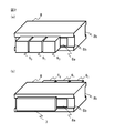
- FIG. 1 It is a schematic diagram which shows the structure of the optical transmission system provided with the optical multiplexer / demultiplexer by Embodiment 1 of this invention. It is a perspective view which shows the structure of the optical multiplexer / demultiplexer by Embodiment 1 of this invention. It is sectional drawing which shows the structure which adhere
- FIG. 1 is a schematic diagram illustrating a configuration of an optical transmission system 100 including an optical multiplexer / demultiplexer 3 according to a first embodiment of the present invention.
- 2 is a perspective view showing the configuration of the optical multiplexer / demultiplexer 3.
- FIG. 2 (a) is a view seen from the side where the optical filter 6j is attached to the holder block 8, and FIG. It is the figure seen from the side which attached the mirror 7 to the holder block 8.
- a lens 2 that converts the optical signal Si
- an optical multiplexer / demultiplexer 3 that combines and outputs the optical signal Si
- a lens 4 that condenses the optical signal Si that has been combined and emitted, and the collected optical signal Si
- the optical filter 6j has a wavelength transmission characteristic of transmitting an optical signal having a wavelength ⁇ i but reflecting other wavelengths.
- the mirror 7 reflects optical signals of all wavelengths.
- the holder block 8 adheres and holds the optical filter 6j and the mirror 7 at predetermined positions on two parallel surfaces via the adhesive layer 9, respectively. As shown in FIG. 2, the holder block 8 is provided with a hollow portion 8a through which the optical signal passes in the recess 8b.
- FIG. 3 is a cross-sectional view showing a structure in which the optical filter 6j and the holder block 8 are bonded by the adhesive layer 9.
- the optical filter 6 j has the adhesive layer 9 so as to straddle the concave portion 8 b in which the hollow portion 8 a is provided at a predetermined position on one parallel surface 8 c of the two parallel surfaces of the holder block 8. Is glued through.
- the mirror 7 is also bonded via an adhesive layer 9 at a predetermined position on the other parallel surface 8d of the two parallel surfaces of the holder block 8 so as to straddle the concave portion 8b provided with the hollow portion 8a.
- the optical multiplexer / demultiplexer 3 operates as an optical multiplexer and an optical demultiplexer, and the configuration of the holder block 8, the optical filter 6j, and the mirror 7 and the manufacturing method thereof are exactly the same. Give an explanation.
- the outgoing beam from the semiconductor laser 1 i is multiplexed and emitted by the optical multiplexer / demultiplexer 3.
- the outgoing beam from the optical multiplexer / demultiplexer 3 is condensed on the optical fiber 5 by the lens 4 and transmitted as a wavelength multiplexed optical signal from the optical transmission device.
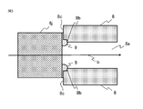
- FIG. 4 is a flowchart showing the manufacturing process of the optical multiplexer / demultiplexer 3.
- FIG. 5 is a cross-sectional view for explaining a method for manufacturing the optical multiplexer / demultiplexer 3.
- gripping jigs 10a and 10b having a pair of parallel surfaces 10ap and 10bp shown in FIG. 5 are used.
- the gripping jigs 10a and 10b are each provided with a suction hole 11 and a heater 17 for vacuum-sucking the mirror 7 and the optical filter 6j in a removable manner.
- the mirror 7 and the optical filters 6 0 , 6 1 , 6 2 are held in the predetermined suction holes 11 of the gripping jigs 10a, 10b by vacuum suction (step S401).
- the mirror 7 and the optical filters 6 0 , 6 1 , 6 2 are arranged by being attracted to a pair of parallel surfaces 10ap, 10bp, so that the mirror 7 and the optical filters 6 0 , 6 1 , 6 2 are The positional relationship parallel to each other can be maintained.
- the holder block 8 formed in advance by applying the adhesive layer 9 at a predetermined position is held between the holding jigs 10a and 10b (step S402).
- the mirror 7 is pressed against the parallel surface 8d of the holder block 8 through the adhesive layer 9 by the pair of parallel surfaces 10ap and 10bp of the gripping jigs 10a and 10b, and the optical filters 6 0 , 6 1 , 6 2 is pressed against the parallel surface 8 c of the holder block 8 through the adhesive layer 9.
- a thermoplastic adhesive is used for example.
- step S403 the thermoplastic adhesive that is the adhesive layer 9 is melted.
- the optical filter 6 0 , 6 1 , 6 2 and the mirror are not pressed and bonded to follow the outer shape of the holder block 8 by pressing with an excessive force but by pressing with an appropriate force and depending on the thickness of the adhesive layer 9. 7 parallelism is maintained.
- step S404 cooling is performed with the holder block 8 being held by the holding jigs 10a and 10b (step S404).
- the optical filter 6 0, 6 1, 6 2 and the mirror 7 in a state pressed against the holder block 8, by cooling the holder block 8, the thermoplastic adhesive is cured, gripping tool 10a, 10b mutually parallel of
- the optical filters 6 0 , 6 1 , 6 2 and the mirror 7 can be bonded and fixed via the adhesive layer 9 in a state in which the parallelism by the pair of surfaces 10 ap and 10 bp is maintained.
- the holder block 8 Since the optical filters 6 0 , 6 1 , 6 2 and the mirror 7 are bonded to the holder block 8 by reflecting the pair of parallel surfaces 10ap, 10bp of the gripping jigs 10a, 10b, the holder block 8 The gap formed between the parallel surfaces 8d and 8c is filled with the adhesive layer 9, and is adjusted by the thickness of the adhesive layer 9. For this reason, the adhesive layer 9 is applied thickly in advance.
- thermoplastic adhesive which is the adhesive layer 9
- the parallel surfaces 8 c, 8 d which are the adhesion surfaces of the holder block 8
- a recess 8b is provided as a relief structure for the thermoplastic adhesive (see FIGS. 2 and 3).
- the temperature and softness of the thermoplastic adhesive becomes more uniform by performing overheating and cooling of the gripping jig 10 in accordance with overheating and cooling of the holder block 8.
- the angle variation of the optical filter and mirror during pressing can be reduced.
- the optical filter 6j is disposed on one surface 10bp of the gripping jigs 10a and 10b having a pair of parallel surfaces, and the other A step of detachably holding the mirror 7 on the surface 10ap, and a holder block 8 provided with an adhesive layer 9 at a position facing the optical filter 6j and the mirror 7 are connected to the pair of surfaces 10ap and 10bp via the adhesive layer 9.
- the gripping jig 10a and 10b are gripped by the gripping jigs 10a and 10b, the gripping jigs 10a and 10b gripping the holder block 8 are heated, and the holder block 8 is gripped.
- 10b is included, so that the parallelism of the optical filter and the mirror is not based on the parallelism of the bonding surface of the holder block but by the parallelism of a pair of parallel surfaces of the holding jig. To be constant, it is unnecessary to use a high-precision holder block without reducing the material cost. Moreover, since all the optical filters and mirrors can be held by the holding jig and bonded to the holder block, it is excellent in mass productivity.
- the optical signal passing part of the holder block is hollow, even if the adhesive is thick, the optical loss of the optical multiplexer / demultiplexer does not increase.
- the adhesive escape structure is formed in the optical filter / mirror bonding part of the holder block, the adhesive oozes out to the optically effective surface of the optical filter and mirror, and the optical loss of the optical multiplexer / demultiplexer is large. It will never be.
- thermoplastic adhesive used as the adhesive layer
- ultraviolet curable adhesive may be used.
- the adhesive layer is cured by irradiating with ultraviolet rays instead of heating.
- the recessed part as a reservoir part of an adhesive agent was provided in the hollow part side of the optical filter of the holder block 8, and the adhesion area
- the holder block 8 may be made of a porous material, and the holder block itself may have an adhesive escape structure. In this case, excess adhesive penetrates into the holder block. Accordingly, it is possible to prevent the adhesive from seeping out to the optically effective surface of the optical filter and the mirror.
- Embodiment 2 the parallelism between the optical filter 6j and the mirror 7 is defined by reflecting the pair of parallel surfaces 10ap and 10bp of the gripping jigs 10a and 10b. Further, a case where the angles of the optical filter 6j and the mirror 7 are adjusted will be described.
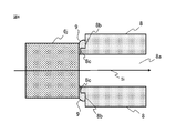
- FIG. 8 is a cross-sectional view for explaining a method for manufacturing the optical multiplexer / demultiplexer 3 according to the second embodiment of the present invention.
- the gripping jigs 10a and 10b are angle adjustment jigs 13a and 13b for finely adjusting the adsorption angle of the optical filter 6j and the mirror 7k to a pair of surfaces 10ap and 10bp parallel to each other. Are provided.
- step S401 of FIG. 4 the angle adjusting jigs 13a and 13b attached to the holding jigs 10a and 10b and finely adjusted in advance to the predetermined suction holes 11 respectively.
- Mirrors 7 1 , 7 2 , 7 3 and optical filters 6 0 , 6 1 , 6 2 are held by vacuum suction.
- the optical filter 61 and the mirror 71, the angle adjusting jig 13b, by 13a the angle is inclined by alpha.
- Other configurations and manufacturing steps are the same as those in the first embodiment, and the description of the same parts is omitted.
- FIG. 9 is a schematic diagram for explaining a method of adjusting the transmission center wavelength of the optical filter in the optical multiplexer / demultiplexer according to the second embodiment of the present invention.
- an optical signal Si indicates a path in the case the inclination of the optical filter 61 was not, the optical signal Si alpha indicating the path when the optical filter 61 is inclined by alpha.
- the optical signal Si alpha reflected by the optical filter 61 is reflected with the angle of 2 ⁇ relative to the optical signal Si when the optical filter 61 is not inclined.
- Optical signals S 1 of the wavelength lambda 1 incident on the optical filter 61 so must become parallel to the optical signal Si alpha reflected by the optical filter 61, as compared with the case where the inclination of the optical filter 61 there is no angle change 2 ⁇ but the optical filter 61 itself is inclined alpha, change of the incident angle is alpha.
- the mirror 71 is inclined by ⁇ so as to cancel the reflection angle by the optical filter 61 of the slope. Therefore, an optical signal Si alpha reflected in the mirror 71 becomes parallel to the optical signal Si when the slope was not.
- Ray of the wavelength lambda 0 which is incident on the optical filter 6 0 is the same as without tilting becomes light filters in parallel with the optical signal Si alpha parallel or light signal Si. It can be adjusted only incident angle to the optical filter 61 independently.
- the incident angle to the optical filter can be adjusted by changing the tilt angle of the angle adjusting jig, and manufacturing variations such as the film thickness of the dielectric multilayer filter formed in the optical filter can be achieved.
- an optical filter having a shifted transmission center wavelength can be used, and the cost of the optical filter can be reduced.
- the holding jig 10a that holds the pair of surfaces parallel to each other, Since each surface 10ap, 10bp of 10b is held via an angle adjusting jig, in addition to the effect of the first embodiment, the incident angle to the optical filter can be adjusted, and the light It is possible to use an optical filter having a transmission center wavelength shifted due to manufacturing variations such as the film thickness of the dielectric multilayer filter formed on the filter, and the cost of the optical filter can be reduced. An effect is obtained.
- Optical multiplexer / demultiplexer 6j optical filter, 7, 7k mirror, 8 holder block, 9 adhesive layer, 10a, 10b gripping jig, 13b, 13a angle adjustment jig
Abstract
This method includes: a step for detachably holding optical filters 6j on one surface 10bp and a mirror 7 on the other surface 10ap of gripping tools 10a, 10b having a pair of mutually parallel surfaces; a step for gripping a holder block 8, provided with adhesive layers 9 in positions facing the optical filters 6j and the mirror 7, in the gripping tools 10a, 10b so that the parallelism of the pair of surfaces 10ap, 10bp is reflected via the adhesive layers 9; a step for heating the gripping tools 10a, 10b in which the holder block 8 is gripped; and a step for cooling the gripping tools 10a, 10b in a state in which the holder block 8 is gripped; the degree of parallelism of the optical filters and the mirror being prescribed by the degree of parallelism of a mutually parallel pair of attachment surfaces of the gripping tools.
Description
この発明は、波長の異なる複数の光信号を合波または分波する光合分波器の製造方法に関するものである。
The present invention relates to a method of manufacturing an optical multiplexer / demultiplexer that multiplexes or demultiplexes a plurality of optical signals having different wavelengths.
光伝送システムにおいては、近年の急激な通信容量の増大に対応するため、複数の波長信号を一本の光ファイバに束ねて、光信号を送受信する波長多重光伝送方式が広く採用されている。この波長多重光伝送方式において、波長の異なる複数の光信号を合波して一本の光ファイバに合波する、あるいは一本の光ファイバの中を伝搬している、波長の異なる複数の光信号を個々の波長に分波するための光学部品が光合分波器である。光合分波器には、導波路に合分波機能を持たせた光導波路タイプと、光フィルタの波長透過特性を利用して合分波機能を実現している空間結合タイプの2種類がある。空間結合タイプの光合分波器は小型で、低光損失な特長を有するため、波長多重光伝送用送受信装置に広く採用されている(例えば、特許文献1参照)。
In an optical transmission system, in order to cope with a rapid increase in communication capacity in recent years, a wavelength division multiplexing optical transmission system that transmits and receives an optical signal by bundling a plurality of wavelength signals into one optical fiber is widely adopted. In this wavelength division multiplexing optical transmission system, a plurality of optical signals having different wavelengths are multiplexed by combining a plurality of optical signals having different wavelengths into one optical fiber, or propagating through one optical fiber. An optical component for demultiplexing a signal into individual wavelengths is an optical multiplexer / demultiplexer. There are two types of optical multiplexers / demultiplexers: an optical waveguide type in which a waveguide has a multiplexing / demultiplexing function, and a spatial coupling type that realizes an multiplexing / demultiplexing function using the wavelength transmission characteristics of an optical filter. . Spatial coupling type optical multiplexers / demultiplexers are small in size and have low optical loss, and are therefore widely used in wavelength division multiplexed optical transmission / reception devices (see, for example, Patent Document 1).
光伝送システムでは、波長多重光伝送装置の信号源である複数の半導体レーザからはそれぞれ波長λi(i=0、1、2、3)の光信号が出射され、レンズにより平行光に変換され、光合波器に入射する。光合波器の複数の光フィルタは、それぞれ対応する光信号の波長λiは透過するが、その他の波長は反射するという波長透過特性を有している。このため、波長λiの光信号はそれぞれ対応する光フィルタを透過し、ホルダブロックに入射し、ミラーと光フィルタの間を反射し、光合波器から出射される。このようにして、半導体レーザからの出射ビームは、光合波器によって合波されて出射される。光合波器からの出射ビームは、レンズにより光ファイバに集光され、光伝送装置より波長多重光信号として送信される。
In the optical transmission system, optical signals having wavelengths λi (i = 0, 1, 2, 3) are emitted from a plurality of semiconductor lasers that are signal sources of the wavelength division multiplexing optical transmission device, and converted into parallel light by a lens. It enters the optical multiplexer. Each of the plurality of optical filters of the optical multiplexer has a wavelength transmission characteristic that transmits the wavelength λi of the corresponding optical signal, but reflects other wavelengths. For this reason, the optical signal of wavelength λi is transmitted through the corresponding optical filter, is incident on the holder block, is reflected between the mirror and the optical filter, and is emitted from the optical multiplexer. In this manner, the outgoing beam from the semiconductor laser is multiplexed by the optical multiplexer and emitted. The outgoing beam from the optical multiplexer is condensed on an optical fiber by a lens and transmitted as a wavelength multiplexed optical signal from an optical transmission device.
ここで、ホルダブロックの光フィルタ・ミラー貼付け面(平行2面)の角度、あるいは光フィルタないしミラーのホルダブロックへの貼付け角度がずれていた場合、光合波器からの出射ビーム角度がずれて、光ファイバへの結合効率が低下する。
Here, if the angle of the optical filter / mirror affixing surface (two parallel surfaces) of the holder block or the affixing angle of the optical filter or mirror to the holder block is shifted, the angle of the outgoing beam from the optical multiplexer is shifted, The coupling efficiency to the optical fiber is reduced.
上記のように、ホルダブロックおよびホルダブロックへの光フィルタ・ミラー貼付けには高い角度精度が要求される。このため、ホルダブロックには高い外形精度が必要になり、部品コストが高くなるという問題があった。また、従来の光合波器は、高精度なホルダブロックの平行2面に光フィルタおよびミラーを、1個ずつ、接着剤の偏りが無くなるように均等に加圧・密着させて接着固定し、製造を行っていた。このため、量産性に問題があった。さらに、波長多重光伝送方式においては、波長間隔を小さくして波長帯域当たりの多重数を増やしたいという要求があり、光フィルタの透過特性(透過中心波長)にも厳しい要求があり、僅かな製造誤差により歩留が発生し、光フィルタの部品コストが高くなるという問題があった。
As described above, high angular accuracy is required for attaching the optical filter and mirror to the holder block and the holder block. For this reason, there is a problem in that the holder block requires high external accuracy and the cost of parts increases. Also, the conventional optical multiplexer is manufactured by attaching and fixing optical filters and mirrors one by one on two parallel surfaces of a high-accuracy holder block by pressing and adhering evenly so that there is no bias in the adhesive. Had gone. For this reason, there was a problem in mass productivity. Furthermore, in the wavelength multiplexing optical transmission system, there is a demand to reduce the wavelength interval and increase the number of multiplexing per wavelength band, and there is a strict demand for the transmission characteristics (transmission center wavelength) of the optical filter. There was a problem that a yield occurred due to an error, and the cost of parts of the optical filter increased.
この発明は、上記のような課題を解決するためになされたもので、組立精度や部品精度を緩和すると共に、量産性の高い光合分波器の製造方法を提供することを目的とする。
The present invention has been made to solve the above-described problems, and has as its object to provide a method for manufacturing an optical multiplexer / demultiplexer with high mass productivity while reducing assembly accuracy and component accuracy.
本発明にかかる光合分波器の製造方法は、平行な一対の面を有する把持治具の一方の面に光フィルタを、他方の面にミラーを、着脱可能に保持する工程と、前記光フィルタと前記ミラーに対向する位置に接着層が設けられたホルダブロックを、前記各接着層を介して前記一対の面の平行が反映されるように前記把持治具で把持する工程とを含むことを特徴とする。
An optical multiplexer / demultiplexer manufacturing method according to the present invention includes a step of detachably holding an optical filter on one surface of a holding jig having a pair of parallel surfaces and a mirror on the other surface, and the optical filter. And gripping the holder block provided with an adhesive layer at a position facing the mirror with the gripping jig so that the parallelism of the pair of surfaces is reflected via each adhesive layer. Features.
この発明によれば、光フィルタとミラーの平行度は、把持治具の平行な一対の面の平行度によって規定されるため、高精度なホルダブロックを使用する必要が無く、量産性の高い製造方法を得ることができる。
According to the present invention, since the parallelism of the optical filter and the mirror is defined by the parallelism of the pair of parallel surfaces of the gripping jig, it is not necessary to use a high-precision holder block, and high-productivity manufacturing is possible. You can get the method.
実施の形態1.
図1は、この発明の実施の形態1にかかる光合分波器3を備えた光伝送システム100の構成を示す模式図である。図2は、光合分波器3の構成を示す斜視図であり、図2(a)は、ホルダブロック8に光フィルタ6jを取付けた側から見た図であり、図2(b)は、ホルダブロック8にミラー7を取付けた側から見た図である。 Embodiment 1 FIG.
FIG. 1 is a schematic diagram illustrating a configuration of anoptical transmission system 100 including an optical multiplexer / demultiplexer 3 according to a first embodiment of the present invention. 2 is a perspective view showing the configuration of the optical multiplexer / demultiplexer 3. FIG. 2 (a) is a view seen from the side where the optical filter 6j is attached to the holder block 8, and FIG. It is the figure seen from the side which attached the mirror 7 to the holder block 8. FIG.
図1は、この発明の実施の形態1にかかる光合分波器3を備えた光伝送システム100の構成を示す模式図である。図2は、光合分波器3の構成を示す斜視図であり、図2(a)は、ホルダブロック8に光フィルタ6jを取付けた側から見た図であり、図2(b)は、ホルダブロック8にミラー7を取付けた側から見た図である。 Embodiment 1 FIG.
FIG. 1 is a schematic diagram illustrating a configuration of an
図1に示すように、光伝送システムは、波長λiの光信号Siが出射する半導体レーザ1i(i=0、1、2、3)と、半導体レーザ1iから出射された光信号Siを平行光に変換するレンズ2と、光信号Siを合波して出射する光合分波器3と、合波して出射された光信号Siを集光するレンズ4と、集光された光信号Siを送信する光ファイバ5とから構成される。光合分波器3は、平行な2面を有するホルダブロック8に、光フィルタ6j(j=0、1、2)およびミラー7を取り付けた構成となっている。光フィルタ6jは、波長λiの光信号は透過するが、その他の波長は反射するという波長透過特性を有している。ミラー7は、全ての波長の光信号を反射する。ホルダブロック8は、接着層9を介して、平行な2面の所定の位置にそれぞれ光フィルタ6jとミラー7を接着保持する。ホルダブロック8は、図2に示すように、凹部8bに光信号が通過する中空部8aが設けられている。
As shown in FIG. 1, the optical transmission system converts a semiconductor laser 1i (i = 0, 1, 2, 3) from which an optical signal Si having a wavelength λi is emitted and an optical signal Si emitted from the semiconductor laser 1i into parallel light. A lens 2 that converts the optical signal Si, an optical multiplexer / demultiplexer 3 that combines and outputs the optical signal Si, a lens 4 that condenses the optical signal Si that has been combined and emitted, and the collected optical signal Si And an optical fiber 5 for transmission. The optical multiplexer / demultiplexer 3 has a configuration in which an optical filter 6j (j = 0, 1, 2) and a mirror 7 are attached to a holder block 8 having two parallel surfaces. The optical filter 6j has a wavelength transmission characteristic of transmitting an optical signal having a wavelength λi but reflecting other wavelengths. The mirror 7 reflects optical signals of all wavelengths. The holder block 8 adheres and holds the optical filter 6j and the mirror 7 at predetermined positions on two parallel surfaces via the adhesive layer 9, respectively. As shown in FIG. 2, the holder block 8 is provided with a hollow portion 8a through which the optical signal passes in the recess 8b.
図3は、光フィルタ6jとホルダブロック8とを接着層9で接着する構造を示す断面図である。図3に示すように、光フィルタ6jは、ホルダブロック8の平行な2面の一方の平行面8cの所定の位置に、中空部8aが設けられている凹部8bを跨ぐように、接着層9を介して接着されている。図示しないが、ミラー7も、ホルダブロック8の平行な2面の他方の平行面8dの所定の位置に、中空部8aが設けられている凹部8bを跨ぐように、接着層9を介して接着されている。
FIG. 3 is a cross-sectional view showing a structure in which the optical filter 6j and the holder block 8 are bonded by the adhesive layer 9. As shown in FIG. 3, the optical filter 6 j has the adhesive layer 9 so as to straddle the concave portion 8 b in which the hollow portion 8 a is provided at a predetermined position on one parallel surface 8 c of the two parallel surfaces of the holder block 8. Is glued through. Although not shown, the mirror 7 is also bonded via an adhesive layer 9 at a predetermined position on the other parallel surface 8d of the two parallel surfaces of the holder block 8 so as to straddle the concave portion 8b provided with the hollow portion 8a. Has been.
なお、光合分波器3は、光合波器および光分波器として動作し、ホルダブロック8、光フィルタ6jおよびミラー7の構成およびその製造方法は全く同じであり、以下においては光合波器として説明を行う。
The optical multiplexer / demultiplexer 3 operates as an optical multiplexer and an optical demultiplexer, and the configuration of the holder block 8, the optical filter 6j, and the mirror 7 and the manufacturing method thereof are exactly the same. Give an explanation.
光伝送システム100においては、波長多重光伝送装置の信号源である半導体レーザ1i(i=0、1、2、3)からは波長λiの光信号Siが出射され、レンズ2により平行光に変換され、光合分波器3に入射する。光合分波器3の光フィルタ6j(j=0、1、2)は、対応する光信号の波長λiは透過するが、その他の波長は反射するという波長透過特性を有している。このため、波長λiの光信号は光フィルタ6jを透過し、ホルダブロック8に入射し、ミラー7と光フィルタ6jの間を反射し、光合分波器3から出射される。このようにして、半導体レーザ1iからの出射ビームは、光合分波器3によって合波されて出射される。光合分波器3からの出射ビームは、レンズ4により光ファイバ5に集光され、光伝送装置より波長多重光信号として送信される。
In the optical transmission system 100, an optical signal Si having a wavelength λi is emitted from a semiconductor laser 1i (i = 0, 1, 2, 3) which is a signal source of a wavelength division multiplexing optical transmission device, and converted into parallel light by a lens 2. And enters the optical multiplexer / demultiplexer 3. The optical filter 6j (j = 0, 1, 2) of the optical multiplexer / demultiplexer 3 has a wavelength transmission characteristic that transmits the wavelength λi of the corresponding optical signal but reflects other wavelengths. For this reason, the optical signal having the wavelength λi passes through the optical filter 6j, enters the holder block 8, reflects between the mirror 7 and the optical filter 6j, and is emitted from the optical multiplexer / demultiplexer 3. In this way, the outgoing beam from the semiconductor laser 1 i is multiplexed and emitted by the optical multiplexer / demultiplexer 3. The outgoing beam from the optical multiplexer / demultiplexer 3 is condensed on the optical fiber 5 by the lens 4 and transmitted as a wavelength multiplexed optical signal from the optical transmission device.
次に、この発明の実施の形態1にかかる光合分波器3の製造方法について説明する。図4は、光合分波器3の製造工程を示すフローチャート図である。図5は、光合分波器3の製造方法を説明するための断面図である。光合分波器3の製造には、図5に示す、互いに平行な一対の面10ap、10bpを有する把持治具10a、10bを用いる。把持治具10a、10bには、それぞれミラー7および光フィルタ6jを着脱可能に真空吸着するための吸着孔11と、ヒーター17が備えられている。
Next, a method for manufacturing the optical multiplexer / demultiplexer 3 according to the first embodiment of the present invention will be described. FIG. 4 is a flowchart showing the manufacturing process of the optical multiplexer / demultiplexer 3. FIG. 5 is a cross-sectional view for explaining a method for manufacturing the optical multiplexer / demultiplexer 3. For manufacturing the optical multiplexer / demultiplexer 3, gripping jigs 10a and 10b having a pair of parallel surfaces 10ap and 10bp shown in FIG. 5 are used. The gripping jigs 10a and 10b are each provided with a suction hole 11 and a heater 17 for vacuum-sucking the mirror 7 and the optical filter 6j in a removable manner.
まず最初に、図4に示すように、把持治具10a、10bのそれぞれ所定の吸着孔11に、ミラー7と光フィルタ60、61、62を真空吸着により保持する(ステップS401)。このとき、互いに平行な一対の面10ap、10bpに吸着してミラー7と光フィルタ60、61、62が配置されることで、ミラー7と光フィルタ60、61、62は互いに平行な位置関係を保つことができる。
First, as shown in FIG. 4, the mirror 7 and the optical filters 6 0 , 6 1 , 6 2 are held in the predetermined suction holes 11 of the gripping jigs 10a, 10b by vacuum suction (step S401). At this time, the mirror 7 and the optical filters 6 0 , 6 1 , 6 2 are arranged by being attracted to a pair of parallel surfaces 10ap, 10bp, so that the mirror 7 and the optical filters 6 0 , 6 1 , 6 2 are The positional relationship parallel to each other can be maintained.
続いて、把持治具10a、10bの間に、接着層9を所定の位置に塗布等で予め形成されたホルダブロック8を把持する(ステップS402)。このとき、把持治具10a、10bの互いに平行な一対の面10ap、10bpにより、ミラー7が接着層9を介してホルダブロック8の平行面8dに押し付けられ、光フィルタ60、61、62が接着層9を介してホルダブロック8の平行面8cに押し付けられる。接着層9は、例えば、熱可塑性接着剤が用いられる。
Subsequently, the holder block 8 formed in advance by applying the adhesive layer 9 at a predetermined position is held between the holding jigs 10a and 10b (step S402). At this time, the mirror 7 is pressed against the parallel surface 8d of the holder block 8 through the adhesive layer 9 by the pair of parallel surfaces 10ap and 10bp of the gripping jigs 10a and 10b, and the optical filters 6 0 , 6 1 , 6 2 is pressed against the parallel surface 8 c of the holder block 8 through the adhesive layer 9. For the adhesive layer 9, for example, a thermoplastic adhesive is used.
次いで、把持治具10a、10bでホルダブロック8を把持したまま、把持治具10a、10bに備えられたヒーター17を加熱し、把持治具10a、10bからホルダブロック8に熱を加えることによって、接着層9である熱可塑性接着剤を溶融させる(ステップS403)。このとき、過度な力による押しつけでホルダブロック8の外形に倣うように接着固定するのではなく、適度な力による押しつけで、接着層9の厚みにより光フィルタ60、61、62とミラー7の平行度が維持されるようにする。
Next, while holding the holder block 8 with the holding jigs 10a and 10b, the heater 17 provided in the holding jigs 10a and 10b is heated, and heat is applied to the holder block 8 from the holding jigs 10a and 10b. The thermoplastic adhesive that is the adhesive layer 9 is melted (step S403). At this time, the optical filter 6 0 , 6 1 , 6 2 and the mirror are not pressed and bonded to follow the outer shape of the holder block 8 by pressing with an excessive force but by pressing with an appropriate force and depending on the thickness of the adhesive layer 9. 7 parallelism is maintained.
最後に、把持治具10a、10bによりホルダブロック8を把持した状態で、冷却する(ステップS404)。光フィルタ60、61、62とミラー7をホルダブロック8に押し付けた状態で、ホルダブロック8を冷却することによって、熱可塑性接着剤が硬化し、把持治具10a、10bの互いに平行な一対の面10ap、10bpによる平行度が維持された状態で光フィルタ60、61、62とミラー7を、接着層9を介して接着・固定することができる。
Finally, cooling is performed with the holder block 8 being held by the holding jigs 10a and 10b (step S404). The optical filter 6 0, 6 1, 6 2 and the mirror 7 in a state pressed against the holder block 8, by cooling the holder block 8, the thermoplastic adhesive is cured, gripping tool 10a, 10b mutually parallel of The optical filters 6 0 , 6 1 , 6 2 and the mirror 7 can be bonded and fixed via the adhesive layer 9 in a state in which the parallelism by the pair of surfaces 10 ap and 10 bp is maintained.
なお、把持治具10a、10bの互いに平行な一対の面10ap、10bpを反映させることにより、光フィルタ60、61、62とミラー7がホルダブロック8に接着されるため、ホルダブロック8の平行面8d、8cとの間にできる空隙は接着層9で満たされ、接着層9の厚さで調整されることとなる。このため、接着層9は、予め厚く塗布される。
Since the optical filters 6 0 , 6 1 , 6 2 and the mirror 7 are bonded to the holder block 8 by reflecting the pair of parallel surfaces 10ap, 10bp of the gripping jigs 10a, 10b, the holder block 8 The gap formed between the parallel surfaces 8d and 8c is filled with the adhesive layer 9, and is adjusted by the thickness of the adhesive layer 9. For this reason, the adhesive layer 9 is applied thickly in advance.
厚く塗布された接着層9により、光フィルタ60、61、62とミラー7をホルダブロック8に押し付けた状態で接着層9である熱可塑性接着剤を溶融させると、余分の熱可塑性接着剤が接着面からはみ出ることになるが、光フィルタ60、61、62およびミラー7の光学有効面にはみ出ないように、ホルダブロック8の接着面である平行面8c、8dには、熱可塑性接着剤の逃げ構造として、凹部8bが設けられている(図2、図3参照)。また、ホルダブロック8の信号通過部は中空となっているため、接着層9が厚くなっても光損失が増加することはない。
When the thermoplastic adhesive which is the adhesive layer 9 is melted in a state where the optical filter 6 0 , 6 1 , 6 2 and the mirror 7 are pressed against the holder block 8 by the thickly applied adhesive layer 9, extra thermoplastic adhesion In order to prevent the agent from protruding from the adhesion surface, but from the optically effective surfaces of the optical filters 6 0 , 6 1 , 6 2 and the mirror 7, the parallel surfaces 8 c, 8 d, which are the adhesion surfaces of the holder block 8, A recess 8b is provided as a relief structure for the thermoplastic adhesive (see FIGS. 2 and 3). Further, since the signal passing portion of the holder block 8 is hollow, the optical loss does not increase even if the adhesive layer 9 is thickened.
また、上記の光合分波器の製造方法において、ホルダブロック8の過熱・冷却に合わせ、把持治具10の過熱・冷却を行うことにより、熱可塑性接着剤の温度・軟らかさがより均一となり、押し付け時の光フィルタおよびミラーの角度バラツキが低減できる。
Further, in the above method of manufacturing an optical multiplexer / demultiplexer, the temperature and softness of the thermoplastic adhesive becomes more uniform by performing overheating and cooling of the gripping jig 10 in accordance with overheating and cooling of the holder block 8. The angle variation of the optical filter and mirror during pressing can be reduced.
以上のように、本実施の形態1にかかる光合分波器3の製造方法によれば、平行な一対の面を有する把持治具10a、10bの一方の面10bpに光フィルタ6jを、他方の面10apにミラー7を、着脱可能に保持する工程と、光フィルタ6jとミラー7に対向する位置に接着層9を設けたホルダブロック8を、接着層9を介して一対の面10ap、10bpの平行が反映されるように把持治具10a、10bで把持する工程と、ホルダブロック8を把持した把持治具10a、10bを加熱する工程と、ホルダブロック8を把持した状態で、把持治具10a、10bを冷却する工程とを含むようにしたので、光フィルタとミラーの平行度は、ホルダブロックの接着面の平行度ではなく、把持治具の互いに平行な一対の面の平行度によって規定されるため、高精度なホルダブロックを使用する必要が無く、部材コストを低減することができる。また、把持治具により全ての光フィルタとミラーを保持して、ホルダブロックに接着することができるため量産性に優れている。さらに、ホルダブロックの光信号通過部が中空となっているため、接着剤が厚くなったとしても光合分波器の光損失が大きくなることはない。また、ホルダブロックの光フィルタ・ミラー接着部には接着剤の逃げ構造が形成されているため、接着剤が光フィルタおよびミラーの光学有効面に染み出して、光合分波器の光損失が大きくなることもない。
As described above, according to the method of manufacturing the optical multiplexer / demultiplexer 3 according to the first embodiment, the optical filter 6j is disposed on one surface 10bp of the gripping jigs 10a and 10b having a pair of parallel surfaces, and the other A step of detachably holding the mirror 7 on the surface 10ap, and a holder block 8 provided with an adhesive layer 9 at a position facing the optical filter 6j and the mirror 7 are connected to the pair of surfaces 10ap and 10bp via the adhesive layer 9. The gripping jig 10a and 10b are gripped by the gripping jigs 10a and 10b, the gripping jigs 10a and 10b gripping the holder block 8 are heated, and the holder block 8 is gripped. 10b is included, so that the parallelism of the optical filter and the mirror is not based on the parallelism of the bonding surface of the holder block but by the parallelism of a pair of parallel surfaces of the holding jig. To be constant, it is unnecessary to use a high-precision holder block without reducing the material cost. Moreover, since all the optical filters and mirrors can be held by the holding jig and bonded to the holder block, it is excellent in mass productivity. Furthermore, since the optical signal passing part of the holder block is hollow, even if the adhesive is thick, the optical loss of the optical multiplexer / demultiplexer does not increase. In addition, since the adhesive escape structure is formed in the optical filter / mirror bonding part of the holder block, the adhesive oozes out to the optically effective surface of the optical filter and mirror, and the optical loss of the optical multiplexer / demultiplexer is large. It will never be.
なお、上記実施の形態では接着層として熱可塑性接着剤を用いた例を示したが、紫外線硬化型の接着剤を用いても良い。その場合、接着層の硬化には加熱ではなく、紫外線を照射することになる。
In the above embodiment, an example in which a thermoplastic adhesive is used as the adhesive layer is shown, but an ultraviolet curable adhesive may be used. In this case, the adhesive layer is cured by irradiating with ultraviolet rays instead of heating.
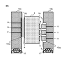
また、上記実施の形態ではホルダブロック8の接着剤の逃げ構造としてホルダブロック8の光フィルタおよびミラーの接着領域の中空部側に接着剤の溜まり部としての凹部を設けたが、図6に示すように、ホルダブロック8の光フィルタおよびミラーの接着領域の中空部とは反対側に凹部を設けても同様の効果が得られる。
Moreover, in the said embodiment, although the recessed part as a reservoir part of an adhesive agent was provided in the hollow part side of the optical filter of the holder block 8, and the adhesion area | region of a mirror as an escape structure of the adhesive agent of the holder block 8, it shows in FIG. As described above, the same effect can be obtained even if a concave portion is provided on the side opposite to the hollow portion of the adhesive region of the optical filter and mirror of the holder block 8.
さらに、図7に示すように、ホルダブロック8が多孔質の材料からなり、ホルダブロック自体が接着剤の逃げ構造となっていても良く、この場合、ホルダブロック内部に余分な接着剤が染み込んでいくことにより、接着剤が光フィルタおよびミラーの光学有効面に染み出してくることを防ぐことが出来る。
Further, as shown in FIG. 7, the holder block 8 may be made of a porous material, and the holder block itself may have an adhesive escape structure. In this case, excess adhesive penetrates into the holder block. Accordingly, it is possible to prevent the adhesive from seeping out to the optically effective surface of the optical filter and the mirror.
実施の形態2.
実施の形態1では、把持治具10a、10bの互いに平行な一対の面10ap、10bpを反映させることにより光フィルタ6jとミラー7の平行度を規定する場合を示したが、実施の形態2では、さらに光フィルタ6jおよびミラー7の角度を調整する場合について説明する。Embodiment 2. FIG.
In the first embodiment, the parallelism between theoptical filter 6j and the mirror 7 is defined by reflecting the pair of parallel surfaces 10ap and 10bp of the gripping jigs 10a and 10b. Further, a case where the angles of the optical filter 6j and the mirror 7 are adjusted will be described.
実施の形態1では、把持治具10a、10bの互いに平行な一対の面10ap、10bpを反映させることにより光フィルタ6jとミラー7の平行度を規定する場合を示したが、実施の形態2では、さらに光フィルタ6jおよびミラー7の角度を調整する場合について説明する。
In the first embodiment, the parallelism between the
図8は、この発明の実施の形態2にかかる光合分波器3の製造方法を説明するための断面図である。この実施の形態2の光合分波器3においては、図8に示すように、ホルダブロック8には、分割されたミラー7k(k=1、2、3)が取り付けられる構成となっている。光合分波器3の製造方法においては、把持治具10a、10bは、互いに平行な一対の面10ap、10bpに、光フィルタ6jおよびミラー7kの吸着角度を微調整する角度調整治具13a、13bがそれぞれ設けられている。光合分波器3の製造工程では、図4のステップS401で、把持治具10a、10bに取り付けられた、予め角度が微調整された角度調整治具13a、13bのそれぞれ所定の吸着孔11に、ミラー71、72、73と光フィルタ60、61、62を真空吸着により保持する。図8では、光フィルタ61とミラー71は、角度調整治具13b、13aにより、角度がαだけ傾けられている。その他の構成および製造工程については、実施の形態1と同様であり、同様部分の説明は省略する。
FIG. 8 is a cross-sectional view for explaining a method for manufacturing the optical multiplexer / demultiplexer 3 according to the second embodiment of the present invention. In the optical multiplexer / demultiplexer 3 according to the second embodiment, as shown in FIG. 8, the holder block 8 is configured to be attached with divided mirrors 7 k (k = 1, 2, 3). In the manufacturing method of the optical multiplexer / demultiplexer 3, the gripping jigs 10a and 10b are angle adjustment jigs 13a and 13b for finely adjusting the adsorption angle of the optical filter 6j and the mirror 7k to a pair of surfaces 10ap and 10bp parallel to each other. Are provided. In the manufacturing process of the optical multiplexer / demultiplexer 3, in step S401 of FIG. 4, the angle adjusting jigs 13a and 13b attached to the holding jigs 10a and 10b and finely adjusted in advance to the predetermined suction holes 11 respectively. , Mirrors 7 1 , 7 2 , 7 3 and optical filters 6 0 , 6 1 , 6 2 are held by vacuum suction. In Figure 8, the optical filter 61 and the mirror 71, the angle adjusting jig 13b, by 13a, the angle is inclined by alpha. Other configurations and manufacturing steps are the same as those in the first embodiment, and the description of the same parts is omitted.
この実施の形態2の光合分波器3の製造方法を用いることにより、光フィルタの透過中心波長は、光フィルタへの入射角を変えることによって調整することが出来る。図9は、この発明の実施の形態2による光合分波器での光フィルタの透過中心波長の調整方法を説明するための模式図である。
By using the method of manufacturing the optical multiplexer / demultiplexer 3 of the second embodiment, the transmission center wavelength of the optical filter can be adjusted by changing the incident angle to the optical filter. FIG. 9 is a schematic diagram for explaining a method of adjusting the transmission center wavelength of the optical filter in the optical multiplexer / demultiplexer according to the second embodiment of the present invention.
図9に示すように、光信号Siは光フィルタ61の傾きが無かった場合の経路を示し、光信号Siαは光フィルタ61をαだけ傾けた場合の経路を示す。光フィルタ61で反射された光信号Siαは、光フィルタ61が傾いていない時の光信号Siに対して2αの角度が付いて反射する。光フィルタ61に入射する波長λ1の光信号S1は、光フィルタ61で反射した光信号Siαと平行にならなければならないので、光フィルタ61の傾きが無かった場合に比べて角度が2α変わるが、光フィルタ61自体もα傾いているので、入射角度の変化はαである。
As shown in FIG. 9, an optical signal Si indicates a path in the case the inclination of the optical filter 61 was not, the optical signal Si alpha indicating the path when the optical filter 61 is inclined by alpha. The optical signal Si alpha reflected by the optical filter 61, is reflected with the angle of 2α relative to the optical signal Si when the optical filter 61 is not inclined. Optical signals S 1 of the wavelength lambda 1 incident on the optical filter 61, so must become parallel to the optical signal Si alpha reflected by the optical filter 61, as compared with the case where the inclination of the optical filter 61 there is no angle change 2α but the optical filter 61 itself is inclined alpha, change of the incident angle is alpha.
一方、ミラー71は光フィルタ61の傾きによる反射角を打ち消すようにαだけ傾いている。このため、ミラー71において反射された光信号Siαは、傾きが無かった時の光信号Siと平行になる。光フィルタ60に入射する波長λ0の光線は光信号Siαと平行すなわち光信号Siと平行になり光フィルタを傾けなかった場合と同じになる。光フィルタ61への入射角だけを独立に調整することができる。
On the other hand, the mirror 71 is inclined by α so as to cancel the reflection angle by the optical filter 61 of the slope. Therefore, an optical signal Si alpha reflected in the mirror 71 becomes parallel to the optical signal Si when the slope was not. Ray of the wavelength lambda 0 which is incident on the optical filter 6 0 is the same as without tilting becomes light filters in parallel with the optical signal Si alpha parallel or light signal Si. It can be adjusted only incident angle to the optical filter 61 independently.
同様に、光フィルタ62への入射角を調整したい場合には、光フィルタ62とミラー72を吸着する角度調整治具の角度を変えることによって、光フィルタ62への入射角を調整することができる。また、光フィルタ60への入射角を調整したい場合には、対向するミラーが無いので、光フィルタ60を吸着する角度調整治具の角度だけを変えることによって、光フィルタ60への入射角を調整することができる。
Similarly, if you want to adjust the angle of incidence on the optical filter 6 2, by changing the angle of the angle adjusting jig adsorbs optical filter 6 2 and the mirror 7 2, adjusting the incident angle to the optical filter 6 2 can do. When it is desired to adjust the angle of incidence on the optical filter 6 0, since the mirror facing no incidence of by changing the angle of the angle adjusting jig for attracting an optical filter 6 0, the optical filter 6 0 The corner can be adjusted.
このように、角度調整治具の傾き角を変えることによって光フィルタへの入射角を調整することが出来るようになり、光フィルタに形成されている誘電体多層膜フィルタの膜厚などの製造バラツキによって生じる透過中心波長がずれた光フィルタも使用することが出来るようになり、光フィルタの部材コストを低減することが出来るという効果が得られる。
As described above, the incident angle to the optical filter can be adjusted by changing the tilt angle of the angle adjusting jig, and manufacturing variations such as the film thickness of the dielectric multilayer filter formed in the optical filter can be achieved. Thus, an optical filter having a shifted transmission center wavelength can be used, and the cost of the optical filter can be reduced.
以上のように、本実施の形態2にかかる光合分波器3の製造方法によれば、光フィルタ6jとミラー7を保持する工程で、互いに平行な一対の面で把持する把持治具10a、10bの各面10ap、10bpと、角度調整治具を介して保持するようにしたので、実施の形態1の効果に加えて、光フィルタへの入射角を調整することが出来るようになり、光フィルタに形成されている誘電体多層膜フィルタの膜厚などの製造バラツキによって生じる透過中心波長がずれた光フィルタも使用することが出来るようになり、光フィルタの部材コストを低減することが出来るという効果が得られる。
As described above, according to the method of manufacturing the optical multiplexer / demultiplexer 3 according to the second embodiment, in the step of holding the optical filter 6j and the mirror 7, the holding jig 10a that holds the pair of surfaces parallel to each other, Since each surface 10ap, 10bp of 10b is held via an angle adjusting jig, in addition to the effect of the first embodiment, the incident angle to the optical filter can be adjusted, and the light It is possible to use an optical filter having a transmission center wavelength shifted due to manufacturing variations such as the film thickness of the dielectric multilayer filter formed on the filter, and the cost of the optical filter can be reduced. An effect is obtained.
なお、この発明は、発明の範囲内において、各実施の形態を自由に組み合わせたり、各実施の形態を適宜、変形、省略することが可能である。
It should be noted that the present invention can be freely combined with each other within the scope of the invention, and each embodiment can be appropriately modified or omitted.
3 光合分波器、6j 光フィルタ、7、7k ミラー、8 ホルダブロック、9 接着層、10a、10b 把持治具、13b、13a 角度調整治具
3. Optical multiplexer / demultiplexer, 6j optical filter, 7, 7k mirror, 8 holder block, 9 adhesive layer, 10a, 10b gripping jig, 13b, 13a angle adjustment jig
Claims (6)
- 平行な一対の面を有する把持治具の一方の面に光フィルタを、他方の面にミラーを、着脱可能に保持する工程と、
前記光フィルタと前記ミラーに対向する位置に接着層が設けられたホルダブロックを、前記各接着層を介して前記一対の面の平行が反映されるように前記把持治具で把持する工程と
を含むことを特徴とする光合分波器の製造方法。 A step of detachably holding an optical filter on one surface of a gripping jig having a pair of parallel surfaces and a mirror on the other surface;
Gripping a holder block provided with an adhesive layer at a position facing the optical filter and the mirror with the gripping jig so that the parallelism of the pair of surfaces is reflected through the adhesive layers. A method of manufacturing an optical multiplexer / demultiplexer, comprising: - 前記光フィルタと前記ミラーを保持する工程で、前記把持治具の前記各面と角度調整治具を介して保持することを特徴とする請求項1に記載の光合分波器の製造方法。 2. The method of manufacturing an optical multiplexer / demultiplexer according to claim 1, wherein in the step of holding the optical filter and the mirror, the optical filter and the mirror are held via the surfaces and the angle adjusting jig.
- 前記接着層は、熱可塑性接着剤からなり、
前記ホルダブロックを把持した前記把持治具を加熱する工程と、
前記ホルダブロックを把持した状態で、前記把持治具を冷却する工程と
を更に含むことを特徴とする請求項1または請求項2に記載の光合分波器の製造方法。 The adhesive layer is made of a thermoplastic adhesive,
Heating the gripping jig that grips the holder block;
The method for manufacturing an optical multiplexer / demultiplexer according to claim 1, further comprising: cooling the gripping jig while gripping the holder block. - 前記接着層は、紫外線硬化型の接着剤からなり、
前記ホルダブロックを把持した状態で、前記接着層に紫外線を照射する工程と
を更に含むことを特徴とする請求項1または請求項2に記載の光合分波器の製造方法。 The adhesive layer is made of an ultraviolet curable adhesive,
The method for manufacturing an optical multiplexer / demultiplexer according to claim 1, further comprising: irradiating the adhesive layer with ultraviolet light while holding the holder block. - 前記ホルダブロックは、前記光フィルタと前記ミラーとを経由する光信号の通過部が中空であることを特徴とする請求項1から請求項4のいずれか1項に記載の光合分波器の製造方法。 5. The optical multiplexer / demultiplexer according to claim 1, wherein the holder block has a hollow optical signal passing portion that passes through the optical filter and the mirror. 6. Method.
- 前記ホルダブロックは、前記光フィルタおよび前記ミラーを接着する領域の一部に、凹部が形成されていることを特徴とする請求項1から請求項5のいずれか1項に記載の光合分波器の製造方法。 The optical multiplexer / demultiplexer according to any one of claims 1 to 5, wherein the holder block has a recess formed in a part of a region where the optical filter and the mirror are bonded. Manufacturing method.
Priority Applications (4)
| Application Number | Priority Date | Filing Date | Title |
|---|---|---|---|
| PCT/JP2018/004631 WO2019155609A1 (en) | 2018-02-09 | 2018-02-09 | Method for manufacturing optical multiplexer/demultiplexer |
| JP2018530188A JP6416448B1 (en) | 2018-02-09 | 2018-02-09 | Manufacturing method of optical multiplexer / demultiplexer |
| US16/769,212 US11360266B2 (en) | 2018-02-09 | 2018-02-09 | Method for manufacturing optical multiplexer/demultiplexer |
| CN201880088563.7A CN111684337B (en) | 2018-02-09 | 2018-02-09 | Method for manufacturing optical multiplexer/demultiplexer |
Applications Claiming Priority (1)
| Application Number | Priority Date | Filing Date | Title |
|---|---|---|---|
| PCT/JP2018/004631 WO2019155609A1 (en) | 2018-02-09 | 2018-02-09 | Method for manufacturing optical multiplexer/demultiplexer |
Publications (1)
| Publication Number | Publication Date |
|---|---|
| WO2019155609A1 true WO2019155609A1 (en) | 2019-08-15 |
Family
ID=64017211
Family Applications (1)
| Application Number | Title | Priority Date | Filing Date |
|---|---|---|---|
| PCT/JP2018/004631 WO2019155609A1 (en) | 2018-02-09 | 2018-02-09 | Method for manufacturing optical multiplexer/demultiplexer |
Country Status (4)
| Country | Link |
|---|---|
| US (1) | US11360266B2 (en) |
| JP (1) | JP6416448B1 (en) |
| CN (1) | CN111684337B (en) |
| WO (1) | WO2019155609A1 (en) |
Families Citing this family (1)
| Publication number | Priority date | Publication date | Assignee | Title |
|---|---|---|---|---|
| JP6804698B1 (en) * | 2020-02-21 | 2020-12-23 | 三菱電機株式会社 | Integrated optical module |
Citations (3)
| Publication number | Priority date | Publication date | Assignee | Title |
|---|---|---|---|---|
| JPS63223607A (en) * | 1987-03-12 | 1988-09-19 | Fujitsu Ltd | Method for sticking filter film to optical multiplexing, demultiplexing and branching circuit |
| JP2007163631A (en) * | 2005-12-12 | 2007-06-28 | Nippon Telegr & Teleph Corp <Ntt> | Optical multiplexer/demultiplexer |
| WO2017033230A1 (en) * | 2015-08-21 | 2017-03-02 | 三菱電機株式会社 | Optical component and optical module |
Family Cites Families (17)
| Publication number | Priority date | Publication date | Assignee | Title |
|---|---|---|---|---|
| JP2880619B2 (en) * | 1993-04-14 | 1999-04-12 | 信越化学工業株式会社 | Apparatus and method for manufacturing optical multiplexing / demultiplexing coupler |
| US5859717A (en) * | 1997-02-14 | 1999-01-12 | Corning Oca Corporation | Multiplexing device with precision optical block |
| KR100300959B1 (en) * | 1997-07-05 | 2001-10-26 | 윤종용 | Apparatus and method for separating light by using flat plate and method for manufacturing light separating apparatus |
| CN100422777C (en) * | 2002-11-01 | 2008-10-01 | 欧姆龙株式会社 | Optical multiplexer/demultiplexer and production method for optical multiplexer/demultiplexer |
| JP2004206057A (en) * | 2002-11-01 | 2004-07-22 | Omron Corp | Optical multiplexer/demultiplexer and manufacturing method therefor |
| US7466502B2 (en) | 2005-12-07 | 2008-12-16 | Tessera North America, Inc. | Optical wavelength division coupler and associated methods |
| CA2616311C (en) | 2005-07-22 | 2014-09-30 | Tessera North America, Inc. | Optical wavelength division coupler and associated methods |
| US20120050876A1 (en) * | 2010-08-30 | 2012-03-01 | Stanley Electric Co., Ltd. | Dihedral corner reflector array optical element and method for fabricating the same and display device using the same |
| JP5555107B2 (en) * | 2010-09-17 | 2014-07-23 | 株式会社沖データ | LENS ARRAY, LENS UNIT, LED HEAD, EXPOSURE DEVICE, IMAGE FORMING DEVICE, READER, LENS ARRAY MANUFACTURING METHOD AND MOLD |
| CN103676007A (en) * | 2012-09-20 | 2014-03-26 | 诺方(哈尔滨)科技股份有限公司 | Coarse wavelength division multiplexer |
| JP2014095843A (en) | 2012-11-12 | 2014-05-22 | Sumitomo Electric Ind Ltd | Optical multiplexer/demultiplexer and method of manufacturing the same, and optical communication module |
| JP6337478B2 (en) | 2014-01-24 | 2018-06-06 | 株式会社ニコン | Demultiplexing element |
| JP6449429B2 (en) * | 2015-03-05 | 2019-01-09 | 三菱電機株式会社 | Manufacturing method of optical multiplexer |
| KR20160145956A (en) | 2015-06-11 | 2016-12-21 | 주식회사 지피 | Wavelength multiplexing optical receiving module |
| US9857535B2 (en) * | 2015-11-03 | 2018-01-02 | Electronics And Telecommunications Research Institute | Method of packaging multichannel optical receiver module having a sub-mount with an optical block to guide incident parallel light beams and package of the same |
| CN205958795U (en) * | 2016-07-06 | 2017-02-15 | 北极光电(深圳)有限公司 | Novel integrated little optical wave divides and multiplexing subassembly |
| CN109477920B (en) * | 2016-07-12 | 2022-02-08 | 3M创新有限公司 | Optical stack |
-
2018
- 2018-02-09 WO PCT/JP2018/004631 patent/WO2019155609A1/en active Application Filing
- 2018-02-09 US US16/769,212 patent/US11360266B2/en active Active
- 2018-02-09 JP JP2018530188A patent/JP6416448B1/en active Active
- 2018-02-09 CN CN201880088563.7A patent/CN111684337B/en active Active
Patent Citations (3)
| Publication number | Priority date | Publication date | Assignee | Title |
|---|---|---|---|---|
| JPS63223607A (en) * | 1987-03-12 | 1988-09-19 | Fujitsu Ltd | Method for sticking filter film to optical multiplexing, demultiplexing and branching circuit |
| JP2007163631A (en) * | 2005-12-12 | 2007-06-28 | Nippon Telegr & Teleph Corp <Ntt> | Optical multiplexer/demultiplexer |
| WO2017033230A1 (en) * | 2015-08-21 | 2017-03-02 | 三菱電機株式会社 | Optical component and optical module |
Also Published As
| Publication number | Publication date |
|---|---|
| CN111684337B (en) | 2022-04-26 |
| US20210173147A1 (en) | 2021-06-10 |
| US11360266B2 (en) | 2022-06-14 |
| JP6416448B1 (en) | 2018-10-31 |
| JPWO2019155609A1 (en) | 2020-02-27 |
| CN111684337A (en) | 2020-09-18 |
Similar Documents
| Publication | Publication Date | Title |
|---|---|---|
| US6748133B2 (en) | Compact multiplexing/demultiplexing modules | |
| CN109597169B (en) | Method of assembling optical receiver module | |
| US8537468B1 (en) | Ultra compact optical multiplexer or demultiplexer | |
| JP2010186090A (en) | Optical transceiver module | |
| WO2004011981A1 (en) | Apparatus for thermal compensation of an arrayed waveguide grating | |
| JP6509451B1 (en) | Optical module | |
| JP2011209367A (en) | Optical multiplexer/demultiplexer and method for manufacturing the same | |
| US20200057212A1 (en) | Bonded filter substrates | |
| US10182275B1 (en) | Passive optical subassembly with a signal pitch router | |
| JP6299858B2 (en) | Lens holding structure, lens holder, optical module, and lens holding method | |
| JP6416448B1 (en) | Manufacturing method of optical multiplexer / demultiplexer | |
| EP1389845A2 (en) | Optical branching and inserting module | |
| JP2014137475A (en) | Light receiving module, and manufacturing method thereof | |
| US10469923B2 (en) | Routing band-pass filter for routing optical signals between multiple optical channel sets | |
| JP2017130543A (en) | Optical transmitter and method of manufacturing the same | |
| JP2014137476A (en) | Light receiving module, and manufacturing method thereof | |
| WO2006042449A1 (en) | Assembling type iso-flim double optical fiber head and its producing method | |
| JP3796183B2 (en) | Silica-based optical waveguide parts | |
| JP2008046271A (en) | Method of manufacturing optical module and device of manufacturing optical module | |
| JP3401134B2 (en) | Optical multiplexer / demultiplexer and manufacturing method thereof | |
| US8192093B2 (en) | Optical transmission module and manufacturing method thereof | |
| JP4219677B2 (en) | Manufacturing method of optical device | |
| WO2019142358A1 (en) | Optical multiplexing-demultiplexing device | |
| JP2006133798A (en) | Quartz optical waveguide component | |
| JP2004094242A (en) | Optical module |
Legal Events
| Date | Code | Title | Description |
|---|---|---|---|
| ENP | Entry into the national phase |
Ref document number: 2018530188 Country of ref document: JP Kind code of ref document: A |
|
| 121 | Ep: the epo has been informed by wipo that ep was designated in this application |
Ref document number: 18904839 Country of ref document: EP Kind code of ref document: A1 |
|
| NENP | Non-entry into the national phase |
Ref country code: DE |
|
| 122 | Ep: pct application non-entry in european phase |
Ref document number: 18904839 Country of ref document: EP Kind code of ref document: A1 |