WO2019146152A1 - Inspection device, ptp packaging machine, and calibration method of inspection device - Google Patents
Inspection device, ptp packaging machine, and calibration method of inspection device Download PDFInfo
- Publication number
- WO2019146152A1 WO2019146152A1 PCT/JP2018/033210 JP2018033210W WO2019146152A1 WO 2019146152 A1 WO2019146152 A1 WO 2019146152A1 JP 2018033210 W JP2018033210 W JP 2018033210W WO 2019146152 A1 WO2019146152 A1 WO 2019146152A1
- Authority
- WO
- WIPO (PCT)
- Prior art keywords
- pixel
- imaging
- image data
- inspection
- spectral image
- Prior art date
Links
- 238000007689 inspection Methods 0.000 title claims abstract description 155
- 238000000034 method Methods 0.000 title claims abstract description 107
- 238000004806 packaging method and process Methods 0.000 title claims abstract description 19
- 238000012545 processing Methods 0.000 claims abstract description 119
- 238000001228 spectrum Methods 0.000 claims abstract description 90
- 230000008569 process Effects 0.000 claims abstract description 82
- 238000012937 correction Methods 0.000 claims abstract description 79
- 230000035945 sensitivity Effects 0.000 claims abstract description 38
- 238000004364 calculation method Methods 0.000 claims abstract description 20
- 238000004458 analytical method Methods 0.000 claims abstract description 13
- 230000003595 spectral effect Effects 0.000 claims description 176
- 238000003384 imaging method Methods 0.000 claims description 167
- 239000010408 film Substances 0.000 claims description 100
- 239000006185 dispersion Substances 0.000 claims description 40
- 239000013039 cover film Substances 0.000 claims description 23
- 238000010183 spectrum analysis Methods 0.000 claims description 18
- 238000011049 filling Methods 0.000 claims description 15
- 239000011159 matrix material Substances 0.000 claims description 13
- 230000001678 irradiating effect Effects 0.000 claims description 12
- 238000003702 image correction Methods 0.000 claims description 8
- 238000004611 spectroscopical analysis Methods 0.000 abstract description 2
- 239000003826 tablet Substances 0.000 description 42
- 230000032258 transport Effects 0.000 description 17
- 230000002950 deficient Effects 0.000 description 16
- 238000010586 diagram Methods 0.000 description 16
- 238000013500 data storage Methods 0.000 description 14
- 238000005286 illumination Methods 0.000 description 14
- 239000000203 mixture Substances 0.000 description 14
- 238000010606 normalization Methods 0.000 description 12
- 238000004080 punching Methods 0.000 description 11
- 238000012935 Averaging Methods 0.000 description 10
- 238000004519 manufacturing process Methods 0.000 description 9
- 238000000513 principal component analysis Methods 0.000 description 9
- 238000012360 testing method Methods 0.000 description 8
- 238000010438 heat treatment Methods 0.000 description 7
- 230000003287 optical effect Effects 0.000 description 7
- 239000000463 material Substances 0.000 description 6
- 239000000047 product Substances 0.000 description 6
- 238000011109 contamination Methods 0.000 description 5
- 230000000694 effects Effects 0.000 description 5
- 230000014509 gene expression Effects 0.000 description 5
- 238000012856 packing Methods 0.000 description 5
- 238000005520 cutting process Methods 0.000 description 4
- 238000009826 distribution Methods 0.000 description 4
- 238000003860 storage Methods 0.000 description 4
- 238000012546 transfer Methods 0.000 description 4
- 239000004743 Polypropylene Substances 0.000 description 3
- 229910052782 aluminium Inorganic materials 0.000 description 3
- XAGFODPZIPBFFR-UHFFFAOYSA-N aluminium Chemical compound [Al] XAGFODPZIPBFFR-UHFFFAOYSA-N 0.000 description 3
- 238000007599 discharging Methods 0.000 description 3
- 238000012840 feeding operation Methods 0.000 description 3
- 229910052736 halogen Inorganic materials 0.000 description 3
- 150000002367 halogens Chemical class 0.000 description 3
- 238000011068 loading method Methods 0.000 description 3
- 230000007246 mechanism Effects 0.000 description 3
- 238000000926 separation method Methods 0.000 description 3
- 229910000661 Mercury cadmium telluride Inorganic materials 0.000 description 2
- 230000015572 biosynthetic process Effects 0.000 description 2
- 230000008859 change Effects 0.000 description 2
- 230000007547 defect Effects 0.000 description 2
- 238000005259 measurement Methods 0.000 description 2
- -1 polypropylene Polymers 0.000 description 2
- 229920001155 polypropylene Polymers 0.000 description 2
- 239000004800 polyvinyl chloride Substances 0.000 description 2
- 229920000915 polyvinyl chloride Polymers 0.000 description 2
- 229920005989 resin Polymers 0.000 description 2
- 239000011347 resin Substances 0.000 description 2
- 238000011144 upstream manufacturing Methods 0.000 description 2
- 230000000007 visual effect Effects 0.000 description 2
- YZCKVEUIGOORGS-OUBTZVSYSA-N Deuterium Chemical compound [2H] YZCKVEUIGOORGS-OUBTZVSYSA-N 0.000 description 1
- 230000005540 biological transmission Effects 0.000 description 1
- 238000006243 chemical reaction Methods 0.000 description 1
- 229910052805 deuterium Inorganic materials 0.000 description 1
- 238000011161 development Methods 0.000 description 1
- 230000004069 differentiation Effects 0.000 description 1
- 239000008298 dragée Substances 0.000 description 1
- 238000005516 engineering process Methods 0.000 description 1
- 230000007613 environmental effect Effects 0.000 description 1
- 239000000284 extract Substances 0.000 description 1
- 238000000605 extraction Methods 0.000 description 1
- 239000004744 fabric Substances 0.000 description 1
- 239000011888 foil Substances 0.000 description 1
- 239000004973 liquid crystal related substance Substances 0.000 description 1
- 239000007769 metal material Substances 0.000 description 1
- 238000002156 mixing Methods 0.000 description 1
- 238000012986 modification Methods 0.000 description 1
- 230000004048 modification Effects 0.000 description 1
- 238000010238 partial least squares regression Methods 0.000 description 1
- 238000002360 preparation method Methods 0.000 description 1
- 238000003825 pressing Methods 0.000 description 1
- 239000002994 raw material Substances 0.000 description 1
- 239000000565 sealant Substances 0.000 description 1
- 238000007789 sealing Methods 0.000 description 1
- 239000007787 solid Substances 0.000 description 1
- 239000007940 sugar coated tablet Substances 0.000 description 1
- 239000013589 supplement Substances 0.000 description 1
- 229920006352 transparent thermoplastic Polymers 0.000 description 1
- WFKWXMTUELFFGS-UHFFFAOYSA-N tungsten Chemical compound [W] WFKWXMTUELFFGS-UHFFFAOYSA-N 0.000 description 1
- 229910052721 tungsten Inorganic materials 0.000 description 1
- 239000010937 tungsten Substances 0.000 description 1
- 229910052724 xenon Inorganic materials 0.000 description 1
- FHNFHKCVQCLJFQ-UHFFFAOYSA-N xenon atom Chemical compound [Xe] FHNFHKCVQCLJFQ-UHFFFAOYSA-N 0.000 description 1
Images


Classifications
-
- B—PERFORMING OPERATIONS; TRANSPORTING
- B29—WORKING OF PLASTICS; WORKING OF SUBSTANCES IN A PLASTIC STATE IN GENERAL
- B29C—SHAPING OR JOINING OF PLASTICS; SHAPING OF MATERIAL IN A PLASTIC STATE, NOT OTHERWISE PROVIDED FOR; AFTER-TREATMENT OF THE SHAPED PRODUCTS, e.g. REPAIRING
- B29C51/00—Shaping by thermoforming, i.e. shaping sheets or sheet like preforms after heating, e.g. shaping sheets in matched moulds or by deep-drawing; Apparatus therefor
- B29C51/26—Component parts, details or accessories; Auxiliary operations
- B29C51/266—Auxiliary operations after the thermoforming operation
-
- G—PHYSICS
- G01—MEASURING; TESTING
- G01N—INVESTIGATING OR ANALYSING MATERIALS BY DETERMINING THEIR CHEMICAL OR PHYSICAL PROPERTIES
- G01N21/00—Investigating or analysing materials by the use of optical means, i.e. using sub-millimetre waves, infrared, visible or ultraviolet light
- G01N21/84—Systems specially adapted for particular applications
- G01N21/86—Investigating moving sheets
-
- B—PERFORMING OPERATIONS; TRANSPORTING
- B65—CONVEYING; PACKING; STORING; HANDLING THIN OR FILAMENTARY MATERIAL
- B65B—MACHINES, APPARATUS OR DEVICES FOR, OR METHODS OF, PACKAGING ARTICLES OR MATERIALS; UNPACKING
- B65B5/00—Packaging individual articles in containers or receptacles, e.g. bags, sacks, boxes, cartons, cans, jars
- B65B5/02—Machines characterised by incorporation of means for making the containers or receptacles
-
- B—PERFORMING OPERATIONS; TRANSPORTING
- B65—CONVEYING; PACKING; STORING; HANDLING THIN OR FILAMENTARY MATERIAL
- B65B—MACHINES, APPARATUS OR DEVICES FOR, OR METHODS OF, PACKAGING ARTICLES OR MATERIALS; UNPACKING
- B65B5/00—Packaging individual articles in containers or receptacles, e.g. bags, sacks, boxes, cartons, cans, jars
- B65B5/10—Filling containers or receptacles progressively or in stages by introducing successive articles, or layers of articles
- B65B5/101—Filling containers or receptacles progressively or in stages by introducing successive articles, or layers of articles by gravity
- B65B5/103—Filling containers or receptacles progressively or in stages by introducing successive articles, or layers of articles by gravity for packaging pills or tablets
-
- B—PERFORMING OPERATIONS; TRANSPORTING
- B65—CONVEYING; PACKING; STORING; HANDLING THIN OR FILAMENTARY MATERIAL
- B65B—MACHINES, APPARATUS OR DEVICES FOR, OR METHODS OF, PACKAGING ARTICLES OR MATERIALS; UNPACKING
- B65B57/00—Automatic control, checking, warning, or safety devices
-
- B—PERFORMING OPERATIONS; TRANSPORTING
- B65—CONVEYING; PACKING; STORING; HANDLING THIN OR FILAMENTARY MATERIAL
- B65B—MACHINES, APPARATUS OR DEVICES FOR, OR METHODS OF, PACKAGING ARTICLES OR MATERIALS; UNPACKING
- B65B57/00—Automatic control, checking, warning, or safety devices
- B65B57/10—Automatic control, checking, warning, or safety devices responsive to absence, presence, abnormal feed, or misplacement of articles or materials to be packaged
-
- G—PHYSICS
- G01—MEASURING; TESTING
- G01N—INVESTIGATING OR ANALYSING MATERIALS BY DETERMINING THEIR CHEMICAL OR PHYSICAL PROPERTIES
- G01N21/00—Investigating or analysing materials by the use of optical means, i.e. using sub-millimetre waves, infrared, visible or ultraviolet light
- G01N21/17—Systems in which incident light is modified in accordance with the properties of the material investigated
- G01N21/25—Colour; Spectral properties, i.e. comparison of effect of material on the light at two or more different wavelengths or wavelength bands
- G01N21/31—Investigating relative effect of material at wavelengths characteristic of specific elements or molecules, e.g. atomic absorption spectrometry
- G01N21/35—Investigating relative effect of material at wavelengths characteristic of specific elements or molecules, e.g. atomic absorption spectrometry using infrared light
- G01N21/3563—Investigating relative effect of material at wavelengths characteristic of specific elements or molecules, e.g. atomic absorption spectrometry using infrared light for analysing solids; Preparation of samples therefor
-
- G—PHYSICS
- G01—MEASURING; TESTING
- G01N—INVESTIGATING OR ANALYSING MATERIALS BY DETERMINING THEIR CHEMICAL OR PHYSICAL PROPERTIES
- G01N21/00—Investigating or analysing materials by the use of optical means, i.e. using sub-millimetre waves, infrared, visible or ultraviolet light
- G01N21/17—Systems in which incident light is modified in accordance with the properties of the material investigated
- G01N21/25—Colour; Spectral properties, i.e. comparison of effect of material on the light at two or more different wavelengths or wavelength bands
- G01N21/31—Investigating relative effect of material at wavelengths characteristic of specific elements or molecules, e.g. atomic absorption spectrometry
- G01N21/35—Investigating relative effect of material at wavelengths characteristic of specific elements or molecules, e.g. atomic absorption spectrometry using infrared light
- G01N21/359—Investigating relative effect of material at wavelengths characteristic of specific elements or molecules, e.g. atomic absorption spectrometry using infrared light using near infrared light
-
- G—PHYSICS
- G01—MEASURING; TESTING
- G01N—INVESTIGATING OR ANALYSING MATERIALS BY DETERMINING THEIR CHEMICAL OR PHYSICAL PROPERTIES
- G01N21/00—Investigating or analysing materials by the use of optical means, i.e. using sub-millimetre waves, infrared, visible or ultraviolet light
- G01N21/84—Systems specially adapted for particular applications
- G01N21/88—Investigating the presence of flaws or contamination
- G01N21/93—Detection standards; Calibrating baseline adjustment, drift correction
-
- G—PHYSICS
- G01—MEASURING; TESTING
- G01N—INVESTIGATING OR ANALYSING MATERIALS BY DETERMINING THEIR CHEMICAL OR PHYSICAL PROPERTIES
- G01N21/00—Investigating or analysing materials by the use of optical means, i.e. using sub-millimetre waves, infrared, visible or ultraviolet light
- G01N21/84—Systems specially adapted for particular applications
- G01N21/88—Investigating the presence of flaws or contamination
- G01N21/95—Investigating the presence of flaws or contamination characterised by the material or shape of the object to be examined
- G01N21/9508—Capsules; Tablets
-
- G—PHYSICS
- G06—COMPUTING; CALCULATING OR COUNTING
- G06T—IMAGE DATA PROCESSING OR GENERATION, IN GENERAL
- G06T7/00—Image analysis
- G06T7/0002—Inspection of images, e.g. flaw detection
- G06T7/0004—Industrial image inspection
-
- B—PERFORMING OPERATIONS; TRANSPORTING
- B29—WORKING OF PLASTICS; WORKING OF SUBSTANCES IN A PLASTIC STATE IN GENERAL
- B29C—SHAPING OR JOINING OF PLASTICS; SHAPING OF MATERIAL IN A PLASTIC STATE, NOT OTHERWISE PROVIDED FOR; AFTER-TREATMENT OF THE SHAPED PRODUCTS, e.g. REPAIRING
- B29C2793/00—Shaping techniques involving a cutting or machining operation
- B29C2793/0009—Cutting out
-
- B—PERFORMING OPERATIONS; TRANSPORTING
- B29—WORKING OF PLASTICS; WORKING OF SUBSTANCES IN A PLASTIC STATE IN GENERAL
- B29C—SHAPING OR JOINING OF PLASTICS; SHAPING OF MATERIAL IN A PLASTIC STATE, NOT OTHERWISE PROVIDED FOR; AFTER-TREATMENT OF THE SHAPED PRODUCTS, e.g. REPAIRING
- B29C2793/00—Shaping techniques involving a cutting or machining operation
- B29C2793/009—Shaping techniques involving a cutting or machining operation after shaping
-
- B—PERFORMING OPERATIONS; TRANSPORTING
- B29—WORKING OF PLASTICS; WORKING OF SUBSTANCES IN A PLASTIC STATE IN GENERAL
- B29C—SHAPING OR JOINING OF PLASTICS; SHAPING OF MATERIAL IN A PLASTIC STATE, NOT OTHERWISE PROVIDED FOR; AFTER-TREATMENT OF THE SHAPED PRODUCTS, e.g. REPAIRING
- B29C51/00—Shaping by thermoforming, i.e. shaping sheets or sheet like preforms after heating, e.g. shaping sheets in matched moulds or by deep-drawing; Apparatus therefor
- B29C51/18—Thermoforming apparatus
-
- B—PERFORMING OPERATIONS; TRANSPORTING
- B29—WORKING OF PLASTICS; WORKING OF SUBSTANCES IN A PLASTIC STATE IN GENERAL
- B29C—SHAPING OR JOINING OF PLASTICS; SHAPING OF MATERIAL IN A PLASTIC STATE, NOT OTHERWISE PROVIDED FOR; AFTER-TREATMENT OF THE SHAPED PRODUCTS, e.g. REPAIRING
- B29C51/00—Shaping by thermoforming, i.e. shaping sheets or sheet like preforms after heating, e.g. shaping sheets in matched moulds or by deep-drawing; Apparatus therefor
- B29C51/26—Component parts, details or accessories; Auxiliary operations
- B29C51/46—Measuring, controlling or regulating
-
- B—PERFORMING OPERATIONS; TRANSPORTING
- B29—WORKING OF PLASTICS; WORKING OF SUBSTANCES IN A PLASTIC STATE IN GENERAL
- B29L—INDEXING SCHEME ASSOCIATED WITH SUBCLASS B29C, RELATING TO PARTICULAR ARTICLES
- B29L2031/00—Other particular articles
- B29L2031/712—Containers; Packaging elements or accessories, Packages
-
- B—PERFORMING OPERATIONS; TRANSPORTING
- B65—CONVEYING; PACKING; STORING; HANDLING THIN OR FILAMENTARY MATERIAL
- B65B—MACHINES, APPARATUS OR DEVICES FOR, OR METHODS OF, PACKAGING ARTICLES OR MATERIALS; UNPACKING
- B65B9/00—Enclosing successive articles, or quantities of material, e.g. liquids or semiliquids, in flat, folded, or tubular webs of flexible sheet material; Subdividing filled flexible tubes to form packages
- B65B9/02—Enclosing successive articles, or quantities of material between opposed webs
- B65B9/04—Enclosing successive articles, or quantities of material between opposed webs one or both webs being formed with pockets for the reception of the articles, or of the quantities of material
- B65B9/045—Enclosing successive articles, or quantities of material between opposed webs one or both webs being formed with pockets for the reception of the articles, or of the quantities of material for single articles, e.g. tablets
-
- G—PHYSICS
- G01—MEASURING; TESTING
- G01N—INVESTIGATING OR ANALYSING MATERIALS BY DETERMINING THEIR CHEMICAL OR PHYSICAL PROPERTIES
- G01N21/00—Investigating or analysing materials by the use of optical means, i.e. using sub-millimetre waves, infrared, visible or ultraviolet light
- G01N21/84—Systems specially adapted for particular applications
- G01N21/86—Investigating moving sheets
- G01N2021/869—Plastics or polymeric material, e.g. polymers orientation in plastic, adhesive imprinted band
-
- G—PHYSICS
- G01—MEASURING; TESTING
- G01N—INVESTIGATING OR ANALYSING MATERIALS BY DETERMINING THEIR CHEMICAL OR PHYSICAL PROPERTIES
- G01N2201/00—Features of devices classified in G01N21/00
- G01N2201/12—Circuits of general importance; Signal processing
- G01N2201/127—Calibration; base line adjustment; drift compensation
Definitions
- the present invention relates to an inspection apparatus that performs mixture inspection and the like of different varieties using spectral analysis, a PTP packaging machine provided with the same, and a calibration method of the inspection apparatus.
- a PTP sheet is composed of a container film having a pocket formed therein to be filled with an object such as a tablet, and a cover film attached to the container film so as to seal the open side of the pocket.
- near infrared light L 1 is applied from a light source such as a halogen lamp to the target 83 filled in the pocket 82 of the container film 81 in the manufacturing process of the PTP sheet. Irradiate.
- the reflected light L 2 reflected from the object 83, etc. is collected by the optical lens 85, it becomes parallel light L 3.
- the light passing through the slit 86 becomes a strip-like slit light L 4 , and enters into a spectroscope (prism) 87 as a spectroscope.
- Slit light L 4 incident on the spectroscope 87 is dispersed into light of each wavelength component, the spectrum on the light receiving surface 89 of the image pickup device 88 (spectrum image) is projected as L 5.
- the spectrum on the light receiving surface 89 of the image pickup device 88 (spectrum image) is projected as L 5.
- near infrared light in a wavelength band of 1300 nm to 2000 nm is separated into several tens to several hundreds bands with wavelength resolution of 1 nm to 10 nm.
- each wavelength component of the spectrum and L 5 is projected to different positions on the light receiving surface 89 of the image sensor 88. Then, it is possible to detect the contamination of different varieties spectral data obtained by imaging the spectrum L 5 by principal component analysis.
- an imaging element such as a CCD area sensor is composed of a plurality of light receiving elements arranged in a matrix, it is necessary to correct variations in sensitivity based on the characteristics of the individual light receiving elements.
- the luminance value of each pixel of image data obtained by imaging a reference plate irradiated with light having uniform intensity (uniform light) is averaged over all pixels It is known to divide by the luminance value to obtain the sensitivity value of the coordinate position corresponding to the pixel, and to divide the luminance value of each pixel of the acquired inspection image data by the sensitivity value related to the pixel at the time of inspection. (See, for example, the prior art of Patent Document 2).
- the luminance value of each pixel is corrected by multiplying the luminance value (measurement value) of each pixel of the inspection image data acquired at the time of inspection by the correction value related to the pixel, a pixel having a large correction value At (for example, 100), the noise included in the measurement value is larger (for example, 100 times larger) with respect to the pixel (for example, 1) having a smaller correction value. That is, the noise level is largely different depending on the wavelength component. As a result, appropriate spectral data can not be obtained, which may reduce inspection accuracy.
- the present invention has been made in view of the above circumstances, and an object thereof is to provide an inspection device, a PTP packaging machine, and a calibration method of the inspection device capable of improving the inspection accuracy relating to an inspection using spectral analysis. It is to do.
- An irradiation unit capable of irradiating near infrared light to the object;
- Spectroscopic means capable of dispersing the reflected light reflected from the object irradiated with the near infrared light;
- the imaging device includes: an imaging device in which a plurality of light receiving devices are arranged in a matrix; and an imaging device capable of imaging a spectrum relating to the reflected light dispersed by the dispersing device;
- An inspection apparatus for performing a predetermined inspection for example, different-mixture inspection
- spectral analysis based on spectral image data acquired by the imaging unit,
- Each pixel row orthogonal to the wavelength dispersion direction of the spectral spectrum and / or the wavelength dispersion direction in reference spectral image data obtained by imaging the spectral spectrum of a predetermined reference object (for example, a reference plate) by the imaging means and acquired
- predetermined arithmetic processing for example, addition processing, averaging processing, normalization processing, etc.
- the average wavelength sensitivity characteristic of the image pickup device is grasped by executing predetermined arithmetic processing on the reference spectral image data and obtaining the characteristic of each pixel row (each wavelength component). be able to.
- the magnitude of the correction value does not change extremely for each pixel, and it is possible to suppress the occurrence of a defect in which the noise level largely differs depending on the wavelength component. As a result, it is possible to improve the inspection accuracy according to the inspection using spectral analysis.
- the output level of the imaging means changes with environmental changes, temperature changes, differences in light sources, etc., it is difficult to set in advance an appropriate correction value at the time of manufacturing the inspection apparatus.
- An irradiation unit capable of irradiating near infrared light to the object;
- Spectroscopic means capable of dispersing the reflected light reflected from the object irradiated with the near infrared light;
- the imaging device includes: an imaging device in which a plurality of light receiving devices are arranged in a matrix; and an imaging device capable of imaging a spectrum relating to the reflected light dispersed by the dispersing device;
- An inspection apparatus for performing a predetermined inspection for example, different-mixture inspection
- spectral analysis based on spectral image data acquired by the imaging unit,
- Each pixel row orthogonal to the wavelength dispersion direction of the spectral spectrum and / or the wavelength dispersion direction in reference spectral image data obtained by imaging the spectral spectrum of a predetermined reference object (for example, a reference plate) by the imaging means and acquired
- predetermined arithmetic processing for example, addition processing, averaging processing, normalization processing, etc.
- the average wavelength sensitivity characteristic of the image pickup device is grasped by executing predetermined arithmetic processing on the reference spectral image data and obtaining the characteristic for each pixel row (for each wavelength component). be able to.
- predetermined arithmetic processing is performed on the reference spectral image data to obtain characteristics of each pixel row (each coordinate position in the imaging region width direction orthogonal to the wavelength dispersion direction), thereby obtaining the imaging region width direction. Average brightness characteristics can be grasped.
- the characteristic related to the pixel row to which the pixel belongs (wavelength sensitivity characteristic), and the characteristic related to the pixel column to which the pixel belongs (imaging area luminance characteristic) Correction values relating to each of the coordinate positions corresponding to each pixel of the reference spectral image data are calculated.
- the noise level of the correction value is less likely to be affected by uneven brightness due to the coordinate position of the imaging region.
- the technique of scanning the sensor not only complicates the structure of the inspection apparatus, but also may require a large amount of time for inspection.
- a PTP packaging machine for producing a PTP sheet in which a predetermined content is accommodated in a pocket portion formed in a container film, and a cover film is attached so as to close the pocket portion, Pocket portion forming means for forming the pocket portion with respect to the container film conveyed in a belt shape; Filling means for filling the contents in the pocket portion; An attachment means for attaching the strip-like cover film so as to close the pocket portion to the container film in which the content is filled in the pocket portion; Separating means (including punching means for punching sheet units) for separating the PTP sheet from a strip (band-like PTP film) in which the cover film is attached to the container film; A PTP packing machine comprising: the inspection device according to the above-mentioned means 1 or 2 which inspects the contents as the inspection object.
- the PTP packaging machine may be configured to include a discharge unit that discharges the PTP sheet determined to be defective by the inspection device.
- the inspection apparatus may be arranged as "a pre-process in which the contents (inspection object) are filled in the pocket portion by the filling means". In such a case, it is possible to eliminate different varieties before filling into the pocket, and to reduce the number of defective PTP sheets.
- the inspection apparatus may be arranged in "the process after the contents (the object to be inspected) are filled in the pocket by the filling means and the process before the cover film is attached by the attaching means". In such a case, the inspection can be performed without interrupting the contents (object to be inspected), and the inspection accuracy can be further improved.
- the inspection apparatus may be arranged in "the process after the cover film is attached by the attaching means and the process before the PTP sheet is detached by the detaching means". In such a case, the inspection can be performed in a state in which the contents (inspection object) are not replaced, and the inspection accuracy can be further improved.
- the inspection apparatus may be disposed in the “process after the PTP sheet is separated by the separation unit”. In such a case, it can be confirmed at the final stage whether or not defective products are mixed.
- An irradiation unit capable of irradiating near infrared light to the object;
- Spectroscopic means capable of dispersing the reflected light reflected from the object irradiated with the near infrared light;
- the imaging device includes: an imaging device in which a plurality of light receiving devices are arranged in a matrix; and an imaging device capable of imaging a spectrum relating to the reflected light dispersed by the dispersing device; It is a calibration method of an inspection apparatus which performs predetermined inspection (for example, different-mixture inspection) using spectral analysis based on spectral image data acquired by the imaging means, Each pixel row orthogonal to the wavelength dispersion direction of the spectral spectrum and / or the wavelength dispersion direction in reference spectral image data obtained by imaging the spectral spectrum of a predetermined reference object (for example, a reference plate) by the imaging means and acquired For each parallel pixel row, predetermined arithmetic processing (for example, addition processing, averaging processing,
- (A) is a perspective view which shows a PTP sheet
- (b) is a perspective view which shows a PTP film. It is a partial expanded sectional view of the pocket part of a PTP sheet.
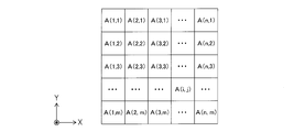
- It is a schematic diagram which shows the data structure of image data two-dimensionally.
- the PTP sheet 1 has a container film 3 provided with a plurality of pocket portions 2 and a cover film 4 attached to the container film 3 so as to close the pocket portions 2. ing. In each pocket 2, one tablet 5 as a content (object to be inspected) is accommodated.
- the container film 3 in the present embodiment is formed of, for example, a transparent thermoplastic resin material such as PP (polypropylene) or PVC (polyvinyl chloride), and has translucency.
- the cover film 4 is made of, for example, an opaque material (for example, aluminum foil or the like) on the surface of which a sealant made of, for example, polypropylene resin is provided.
- the PTP sheet 1 [see FIG. 1 (a)] is formed by punching out a strip-like PTP film 6 [see FIG. 1 (b)] formed of a strip-like container film 3 and a strip-like cover film 4 in sheet form. Manufactured.
- the raw fabric of the strip-like container film 3 is wound in a roll.
- the draw-out end side of the container film 3 wound in a roll is guided by a guide roll 13.
- the container film 3 is hung on the intermittent feed roll 14 at the downstream side of the guide roll 13.
- the intermittent feed roll 14 is connected to a motor which rotates intermittently, and conveys the container film 3 intermittently.
- a heating device 15 and a pocket portion forming device 16 are disposed in order along the transport path of the container film 3. Then, in a state where the container film 3 is heated by the heating device 15 and the container film 3 becomes relatively flexible, the pocket forming device 16 forms a plurality of pocket portions 2 at predetermined positions of the container film 3 ( Pocket part formation process).
- the heating device 15 and the pocket portion forming device 16 constitute a pocket portion forming means in the present embodiment.
- the formation of the pocket portion 2 is performed at an interval between the transport operations of the container film 3 by the intermittent feed roll 14.
- the container film 3 delivered from the intermittent feed roll 14 is stretched in the order of the tension roll 18, the guide roll 19 and the film receiving roll 20.
- the film receiving roll 20 is connected to a motor that rotates at a constant speed, and thus conveys the container film 3 continuously and at a constant speed.
- the tension roll 18 is in a state in which the container film 3 is tensioned by elastic force, and the deflection of the container film 3 due to the difference in the conveying operation of the intermittent feed roll 14 and the film receiving roll 20 is prevented.
- the container film 3 is always kept in tension.
- a tablet filling device 21 is disposed between the guide roll 19 and the film receiving roll 20 along the transport path of the container film 3.
- the tablet filling device 21 has a function as a filling means for automatically filling the pocket 2 with the tablet 5.
- the tablet filling device 21 drops the tablet 5 by opening the shutter at predetermined intervals in synchronization with the transport operation of the container film 3 by the film receiving roll 20, and each pocket portion along with the shutter opening operation. 2 is filled with the tablet 5 (filling step).
- An inspection device 22 is disposed between the tablet filling device 21 and the film receiving roll 20 along the transport path of the container film 3.
- the inspection device 22 is a spectral analysis device which performs inspection using spectral analysis, and is for inspecting contamination of different varieties. Details of the inspection device 22 will be described later.
- the raw material of the cover film 4 formed in a strip shape is wound in a roll on the most upstream side.
- the drawn-out end of the roll-wound cover film 4 is guided by the guide roll 24 and guided toward the heating roll 25.
- the heating roll 25 can be brought into pressure contact with the film receiving roll 20, and the container film 3 and the cover film 4 are fed between the both rolls 20, 25.
- the cover film 4 is attached to the container film 3 and the pocket 2 is closed by the cover film 4 (Attachment process).
- the PTP film 6 as a strip in which the tablets 5 are filled in the respective pocket portions 2 is manufactured.
- the film receiving roll 20 and the heating roll 25 constitute an attachment means in the present embodiment.
- the PTP film 6 delivered from the film receiving roll 20 is stretched in the order of the tension roll 27 and the intermittent feed roll 28. Since the intermittent feed roll 28 is connected to a motor that rotates intermittently, it intermittently transports the PTP film 6.
- the tension roll 27 is in a state in which the PTP film 6 is tensioned by elastic force, and the deflection of the PTP film 6 due to the difference in the transport operation of the film receiving roll 20 and the intermittent feed roll 28 is prevented.
- the PTP film 6 is always kept in tension.
- the PTP film 6 delivered from the intermittent feed roll 28 is stretched in the order of the tension roll 31 and the intermittent feed roll 32. Since the intermittent feed roll 32 is connected to a motor that rotates intermittently, it intermittently transports the PTP film 6.
- the tension roll 31 is in a state in which the PTP film 6 is tensioned by elastic force, and prevents the deflection of the PTP film 6 between the intermittent feed rolls 28 and 32.
- a slit forming device 33 and a marking device 34 are disposed in order along the transport path of the PTP film 6.
- the slit forming device 33 has a function of forming a separating slit at a predetermined position of the PTP film 6.
- the marking device 34 has a function of marking a predetermined position (for example, a tag portion) of the PTP film 6.
- the PTP film 6 delivered from the intermittent feed roll 32 is stretched at the downstream side in the order of the tension roll 35 and the continuous feed roll 36.
- a sheet punching device 37 is disposed between the intermittent feed roll 32 and the tension roll 35 along the transport path of the PTP film 6.
- the sheet punching device 37 has a function as a sheet punching means (separation means) for punching out the outer edge of the PTP film 6 per PTP sheet.
- the PTP sheet 1 punched out by the sheet punching device 37 is conveyed by the pickup conveyor 39 and temporarily stored in the finished product hopper 40 (separation step).
- the PTP sheet 1 determined to be a defective product is separately discharged by a defective sheet discharging mechanism as a discharging unit (not shown).
- a cutting device 41 is disposed downstream of the continuous feed roll 36. And the unnecessary film part 42 which comprises the remaining-material part (scrap part) which remained in strip shape after punching by the sheet punching apparatus 37 is guided to the cutting apparatus 41, after being guided by the said tension roll 35 and continuous feeding roll 36. It is eaten.
- the continuous feed roll 36 is in pressure contact with the driven roll, and performs the transport operation while holding the unnecessary film portion 42.
- the cutting device 41 has a function of cutting the unnecessary film portion 42 into a predetermined size and processing the scrap. The scrap is stored in the scrap hopper 43 and then separately disposed of.
- the rolls 14, 20, 28, 31, 32 and so on have a positional relationship in which the roll surface and the pocket 2 are opposed to each other, but the pocket 2 is on the surface of the intermittent feed roll 14 or the like. Since the recessed part accommodated is formed, the pocket part 2 is not crushed.
- the intermittent feeding operation and the continuous feeding operation can be reliably performed by performing the feeding operation while the pocket portion 2 is accommodated in each concave portion of the intermittent feeding roll 14 or the like.
- FIG. 4 is a block diagram showing the electrical configuration of the inspection apparatus 22
- FIG. 5 is a perspective view schematically showing the arrangement of the inspection apparatus 22. As shown in FIG.
- the inspection device 22 performs various controls, image processing, arithmetic processing, etc. in the inspection device 22 such as drive control of the illumination device 52, the imaging device 53, the illumination device 52 and the imaging device 53. And a control processing unit 54 to be implemented.
- the illumination device 52 and the imaging device 53 are disposed on the side of the pocket 2 opening of the container film 3. That is, in the present embodiment, the different-type mixture inspection is performed from the side of the opening of the pocket portion 2 of the container film 3 before the cover film 4 is attached.
- the illumination device 52 is a known device configured to be capable of emitting near-infrared light, and constitutes an illumination unit in the present embodiment.
- the illumination device 52 is disposed so as to be capable of emitting near-infrared light obliquely from above to a predetermined area on the container film 3 which is continuously transported.
- the illumination device 52 employs a halogen lamp as a light source capable of emitting near infrared light having a continuous spectrum (for example, a near infrared region having a wavelength of 700 to 2500 nm).
- a light source a deuterium discharge tube, a tungsten lamp, a xenon lamp or the like can be used.
- the imaging device 53 includes an optical lens 61, a two-dimensional spectroscope 62 as a spectroscopic means, and a camera 63 as an imaging means.
- the optical lens 61 is composed of a plurality of lenses (not shown) and the like, and is configured to be capable of collimating incident light.
- the optical axis of the optical lens 61 is set along the vertical direction (Z direction).
- the optical lens 61 is set so as to be capable of forming an incident light at the position of a slit 62 a of a two-dimensional spectroscope 62 described later.
- a both-side telecentric lens is adopted as the optical lens 61 is shown, but naturally it may be an image-side telecentric lens.
- the two-dimensional spectroscope 62 is composed of a slit 62a, an incident side lens 62b, a spectral part 62c, and an exit side lens 62d.
- the light splitting unit 62c includes an incident side prism 62ca, a transmission diffraction grating 62cb, and an output side prism 62cc.
- the light passing through the slit 62a is collimated by the incident side lens 62b, and then split by the light separating unit 62c, and a two-dimensional spectral image is formed by the imaging element 65 of the camera 63 described later by the outgoing side lens 62d. It is imaged as (spectral spectrum image).
- the slit 62a is formed into an elongated substantially rectangular shape (linear shape) and the opening width direction (short direction) of the slit 62a is disposed along the film transport direction (Y direction) of the container film 3 It arrange
- the two-dimensional spectroscope 62 disperses the incident light in the opening width direction of the slit 62a, that is, the film transport direction (Y direction). That is, the film transport direction (Y direction) is the wavelength dispersion direction in the present embodiment.
- the camera 63 includes an imaging element 65 having a light receiving surface 65 a in which a plurality of light receiving elements (light receiving portions) 64 are two-dimensionally arranged in a matrix.
- an imaging device 65 a known CCD area sensor having sufficient sensitivity to a wavelength range of, for example, 1300 to 2000 nm in the near infrared range is employed.
- the CCD area sensor for example, a plurality of light receiving elements including photoelectric conversion elements (for example, photodiodes) which are two-dimensionally arranged in a matrix and convert incident light into electric charge corresponding to the light quantity and the respective light receiving elements
- a plurality of vertical transfer units for sequentially transferring the charges accumulated in the vertical direction
- a horizontal transfer unit for sequentially transferring the charges transferred from the vertical transfer unit in the horizontal direction
- the charges transferred from the horizontal transfer unit It is generally known that an output amplifier is provided which converts, amplifies and outputs a voltage.
- the imaging device is not limited to this, and another sensor having sensitivity in the near infrared region may be adopted.
- a CMOS sensor or an MCT (HgCdTe) sensor may be employed.
- the visual field area (imaging area) of the imaging device 53 is a linear area extending along the film width direction (X direction) and is an area including at least the entire film width direction of the container film 3 (FIG. 5 2 (Refer to the dotted line section).
- the visual field area of the imaging device 53 in the film transport direction (Y direction) is an area corresponding to the opening width of the slit 62a. That is, the light (slit light) that has passed through the slit 62 a is an area where an image is formed on the light receiving surface 65 a of the imaging device 65.
- the respective light receiving elements 64 of the imaging element 65 receive the respective wavelength components of the spectrum of the reflected light reflected at each position in the film width direction (X direction) of the container film 3. Then, a signal corresponding to the intensity of the light received by each light receiving element 64 is converted into a digital signal and then output from the camera 63 to the control processing device 54. That is, an image signal (spectral image data) for one screen taken on the entire light receiving surface 65 a of the imaging element 65 is output to the control processing device 54.
- the control processing unit 54 has a CPU for controlling the entire inspection unit 22 and an input / output interface 71 (hereinafter referred to as "CPU etc. 71"), an input unit 72 as an “input unit” comprising a keyboard, a mouse, a touch panel and the like
- CPU etc. 71 an input unit 72 as an "input unit” comprising a keyboard, a mouse, a touch panel and the like
- a display device 73 as a "display means” having a display screen such as a CRT or liquid crystal, an image data storage device 74 for storing various image data etc., an operation result storage device 75 for storing various operation results etc.
- a setting data storage device 76 for storing various information in advance is provided. Each of the devices 72 to 76 is electrically connected to the CPU 71 and the like.
- a CPU 71 and the like are connected to the PTP packaging machine 10 so as to transmit and receive various signals. Thereby, for example, a defective sheet discharging mechanism of the PTP packaging machine 10 can be controlled.
- the image data storage device 74 performs spectral image data acquired by the imaging device 53, corrected spectral image data obtained by correcting the spectral image data, spectral image data obtained based on the corrected spectral image data, and binarization processing
- the stored binary image data, the differential image data after differential processing, and the like are stored.
- the calculation result storage unit 75 stores test result data, statistical data obtained by statistically processing the test result data, and the like. These inspection result data and statistical data can be displayed on the display device 73 as appropriate.
- the setting data storage device 76 stores, for example, the loading vector and determination range used for principal component analysis, the shapes and dimensions of the PTP sheet 1, the pocket portion 2 and the tablet 5, correction values acquired beforehand before the inspection start as described later It is
- This routine is a process for setting in advance a correction value for correcting spectral image data (inspection spectral image data) acquired by the imaging device 53 in the different-type mixture inspection.
- the control processing device 54 first executes the reference plate imaging process (step S01). Specifically, the imaging device 53 performs an imaging process (exposure process) while emitting near-infrared light from the illumination device 52 to a reference plate (not shown) as a reference object. As a result, the spectral spectrum of the reference plate is imaged, and reference spectral image data is acquired.
- the spectral image data acquired by the imaging device 53 has, for example, a data structure as shown in FIG. 8 corresponding to the arrangement configuration of the plurality of light receiving elements 64 in the imaging device 65. That is, a plurality of pixels are arranged in a matrix of m rows and n columns (1 ⁇ i ⁇ n, 1 ⁇ j ⁇ m, i, j, n and m are natural numbers), and each pixel at each coordinate position (i, j) In this structure, a predetermined luminance value is provided.
- the column direction (longitudinal direction) is the wavelength dispersion direction (Y direction)
- the row direction (horizontal direction) is the imaging region width direction (X direction).
- control processing unit 54 executes wavelength-sensitivity characteristic acquisition processing (step S02).
- This process corresponds to the wavelength sensitivity characteristic grasping process in the present embodiment, and the wavelength sensitivity characteristic grasping means in the present embodiment is constituted by the processing function of the control processing unit 54 which executes the process.
- each pixel row (the first to m-th rows) orthogonal to the wavelength dispersion direction of the spectral spectrum in the reference spectral image data acquired in step S01 is Average processing is performed as predetermined arithmetic processing based on the luminance values of the pixels (first to nth columns) to calculate an average luminance value as a predetermined arithmetic value (characteristic) for each pixel row Do.
- the reference spectral image data having the data structure shown in FIG. 8 will be specifically described below as an example.
- the luminance value of the pixel at coordinate (1, 1) the luminance value of the pixel at coordinate (2, 1), the luminance value of the pixel at coordinate (3, 1), ..., the pixel at coordinate (n, 1)
- the average luminance value related to the first pixel row can be obtained. That is, the average luminance level in the imaging region width direction (X direction) orthogonal to the wavelength dispersion direction (Y direction) of the spectral spectrum can be obtained.
- the same processing as described above is performed in each of the other pixel rows.
- the average luminance value of each of the first to m-th pixel rows can be calculated.
- processing such as removal of a greatly deviated value or normalization may be performed as necessary.
- control processing device 54 executes width direction-luminance characteristic acquisition processing (step S03).
- This process corresponds to the imaging area luminance characteristic comprehension process in the present embodiment, and the imaging area luminance characteristic comprehension means in the present embodiment is configured by the processing function of the control processing device 54 that executes this process.
- the pixel columns In the width direction-brightness characteristic acquisition process, in the reference spectral image data acquired in step S01, for each of the pixel columns (first to nth columns) parallel to the wavelength dispersion direction of the spectral spectrum, the pixel columns The averaging process is performed as predetermined arithmetic processing based on the luminance values of the pixels belonging to (the first to m-th rows of pixels), and the average luminance value is calculated as a predetermined arithmetic value (characteristic) for each pixel column. calculate.
- the reference spectral image data having the data structure shown in FIG. 8 will be specifically described below as an example.
- the luminance value of the pixel at coordinate (1, 1), the luminance value of the pixel at coordinate (1, 2), the luminance value of the pixel at coordinate (1, 3), ..., the pixel at coordinate (1, m) Calculate the average value of the brightness values of
- the average luminance value of the first pixel row can be obtained. That is, an average luminance level in the wavelength dispersion direction (Y direction) of the spectral spectrum can be obtained.
- the average luminance level at each position in the imaging region width direction (X direction) by grasping the average luminance value of each pixel row parallel to the wavelength dispersion direction of the spectral spectrum. It can. That is, the average width direction-brightness characteristic (uneven brightness of the illumination light) in the imaging region under the near infrared light emitted from the illumination device 52 can be grasped.
- step S04 the control processing device 54 executes a correction value calculation process.
- This process corresponds to the correction value calculation process in the present embodiment, and the correction value calculation means in the present embodiment is configured by the processing function of the control processing device 54 that executes this process.
- the luminance value of each pixel of the reference spectral image data acquired in step S01 the average luminance value of the pixel row to which the pixel belongs acquired in step S02, and the acquired in step S03 Based on the average luminance value of the pixel row to which the pixel belongs, correction values respectively associated with coordinate positions corresponding to each pixel of the reference spectral image data are calculated.
- the average luminance value of the pixel row to which the pixel belongs is multiplied by the average luminance value of the pixel column to which the pixel belongs, and coordinates corresponding to the pixel
- the “width direction—the wavelength-sensitivity characteristic in consideration of the luminance characteristic (uneven luminance)” at the position is acquired.
- the above-mentioned "width direction-wavelength-sensitivity characteristic considering luminance characteristics (luminance unevenness)" that is, the average luminance value of the pixel row to which a predetermined pixel belongs, and the average luminance value of the pixel column to which the pixel belongs.
- the reference spectral image data having the data structure shown in FIG. 8 will be specifically described below as an example.
- the average luminance value of the first pixel row to which the pixel belongs and the average luminance of the first pixel row to which the pixel belongs The value is multiplied by the value to obtain “width direction-wavelength-sensitivity characteristic in consideration of luminance characteristics (uneven luminance)” related to the coordinates (1, 1).
- the coordinate “1,1” the wavelength—sensitivity characteristic in consideration of the luminance characteristic (uneven luminance) ”is“ 4500 ”.
- width direction—wavelength-sensitivity characteristics considering luminance characteristics (uneven luminance)” related to coordinates (1, 1) that is, the average luminance value related to the first pixel row and the first column
- the value multiplied by the average luminance value of the pixel row is divided by the luminance value of the pixel at coordinate (1, 1) of the reference spectral image data to obtain a correction value of coordinate (1, 1).
- the luminance of the pixel at the coordinate (1, 1) of the reference spectral image data where the “width direction-the wavelength-sensitivity characteristic considering luminance characteristics (uneven luminance)” related to the coordinate (1, 1) is “4500” If the value is "90", the correction value is "50".
- the correction value associated with each coordinate position obtained by the correction value calculation process is stored in the setting data storage device 76 as a storage unit, and the correction value setting routine is ended.
- This routine is a process that is repeatedly executed each time the container film 3 is transported by a predetermined amount.
- step S11 the control processing device 54 irradiates the container film 3 (tablet 5) continuously conveyed with near infrared light from the illumination device 52 (irradiation step), and performs imaging processing (exposure processing) by the imaging device 53 To do).
- control processing device 54 drives and controls the imaging device 53 based on a signal from an encoder (not shown) provided in the PTP packaging machine 10, and the spectral image data captured by the imaging device 53 is stored in the image data storage device 74. Capture to
- the light is reflected in the conveyance direction imaging range W (see FIG. 11) during the execution period (exposure period) of the imaging process in step S11.
- the reflected light enters the imaging device 53. That is, the conveyance direction imaging range W is imaged in one imaging process.
- the reflected light incident on the imaging device 53 is split by the two-dimensional spectroscope 62 (spectroscopic process), and captured as a spectral image (spectral spectrum) by the imaging device 65 of the camera 63 (imaging process).
- the imaging device 65 of the camera 63 imaging process
- the container film 3 tablette 5
- the exposure period exposure period
- FIG. 10 is a schematic view showing a state in which the spectrum L S of the reflected light reflected at the predetermined position on the tablet 5 is projected on the light receiving surface 65 a of the imaging device 65.
- FIG. 10 for convenience, only the spectrum L S of the tablet 5 is shown, and the spectrum of the other part (the container film 3 etc.) is not shown.
- Spectral image (spectral spectrum) data captured by the imaging device 53 is output to the control processing device 54 during an interval period, and stored in the image data storage device 74.
- the interval period is a reading period of image data. That is, the imaging cycle by the imaging device 53 can be represented by the total time of the exposure period which is an execution period of an imaging process, and an interval period.
- step S12 When spectral image data (inspection spectral image data) is acquired by the imaging process of step S11, the control processing device 54 executes a correction process (step S12).
- This process corresponds to the image correction process in the present embodiment, and the processing function of the control processing device 54 that executes this process constitutes the image correction means in the present embodiment.
- inspection spectral image data is corrected based on the correction value acquired in advance by the correction value setting routine and stored in the setting data storage device 76. Specifically, the luminance value of each pixel can be corrected by multiplying the luminance value of each pixel of the inspection spectral image data by the correction value related to the coordinate position corresponding to the pixel.
- the corrected spectral image data (corrected spectral image data) is stored in the image data storage device 74.
- the luminance value of a predetermined pixel of inspection spectral image data is “100” and the correction value related to the coordinate position corresponding to the pixel is “50”, the luminance value of the pixel of the correction spectral image data is It will be "5000".
- step S13 When the corrected spectral image data is acquired by the correction process of step S12, the control processing device 54 executes a spectrum data generation process (step S13).
- spectrum data is generated based on the corrected spectral image data acquired in step S12. Once the spectral data is generated, it is stored in the image data storage device 74, and this routine is temporarily ended.
- This process corresponds to the spectrum data acquisition process in the present embodiment, and the spectrum data acquisition means in the present embodiment is configured by the processing function of the control processing unit 54 that executes this process.
- spectrum data corresponding to each conveyance direction imaging range W is sequentially stored in a time series together with position information of a film conveyance direction (Y direction) and a film width direction (X direction).
- a two-dimensional spectral image Q having spectral data for each pixel is generated (see FIG. 12).
- the spectral image Q is image data in which a plurality of pixels Qa are two-dimensionally arrayed.
- Each pixel Qa includes spectral data [data indicating spectral intensities (luminance values) at a plurality of wavelengths or wavelength bands].
- the control processing device 54 executes an inspection routine.
- the inspection routine is repeatedly performed each time the spectrum image Q in the range corresponding to one PTP sheet 1 is acquired.
- step S21 the control processing device 54 extracts a pixel corresponding to the tablet 5, that is, a pixel (target pixel) Qb to be analyzed among the pixels Qa of the spectrum image Q.
- intensity data luminance value
- a predetermined threshold value a predetermined threshold value
- binarization processing is performed on the spectrum image Q.
- the target pixel Qb is extracted based on the obtained binarized image data (see FIGS. 12 and 14).
- FIG. 14 is an explanatory diagram for explaining the relationship between the conveyance direction imaging range W and the spectral image Q. 12 and 14, the pixels extracted as the target pixel Qb are indicated by oblique lines.
- the pixel extraction method is not limited to this, and other methods may be adopted.
- the target pixel Qb may be extracted by calculating the integrated value of the spectrum data for each pixel Qa and determining whether the value is equal to or greater than a predetermined threshold.
- step S22 the control processing device 54 performs grouping processing of the target pixel Qb obtained in step S21.
- the control processing device 54 performs grouping processing of the target pixel Qb obtained in step S21.
- all adjacent target pixels Qb are made into one group.
- the grouping method is not limited to this, and other methods may be adopted. For example, pixels included in a predetermined range centered on a specific pixel may be determined to be in the same group as the specific pixel.
- object pixel Qb grouped into one is handled as object pixel Qb concerning the same tablet 5 (refer to Drawing 12 and 14).
- the grouped target pixels Qb are surrounded by a thick frame.
- step S23 the control processing device 54 calculates spectral data of the tablet 5 corresponding to the group based on the spectral data of the target pixel Qb grouped in step S22.
- all of the spectral data of the grouped target pixels Qb are used to obtain the average value thereof, and this is calculated as the spectral data (average spectral data) of the tablet 5.
- the present invention is not limited to this, and one or more target pixels Qb may be extracted from the grouped target pixels Qb, and spectral data of the target pixel Qb may be calculated as spectral data of the tablet 5. Also, differentiation processing may be performed as appropriate.
- control processing device 54 executes analysis processing in step S24.
- Such processing corresponds to the analysis step in the present embodiment, and the analysis means in the present embodiment is configured by the function of the control processing device 54 that executes the processing.
- PCA principal component analysis
- step S25 the control processing device 54 performs a determination process to determine whether the target tablet 5 is a non-defective product (the same type) or a defect (different type). More specifically, the principal component scores calculated in step S24 are plotted on the PCA diagram, and if the plotted data falls within the preset non-defective item range, the non-defective item (same kind), if not out of the non-defective item It is determined as
- step S25 The series of processing according to step S25 is executed for all the tablets 5 on the PTP sheet 1, and when there is no tablet 5 which is "defective", the PTP sheet 1 is good. It determines with (step S26) and this routine is complete
- each pixel row (the first to m-th rows) orthogonal to the wavelength dispersion direction of the spectral spectrum in the reference spectral image data Average processing is performed as predetermined arithmetic processing based on the luminance values of the pixels belonging to the pixel row (pixels in the first column to the nth column), and the average luminance is calculated as the predetermined arithmetic value for each pixel row. Calculate the value.
- the average luminance level of each wavelength component of the spectrum can be grasped. That is, the average wavelength-sensitivity characteristic of the imaging device 65 can be grasped.
- the pixels (first row) belonging to the pixel rows An averaging process is performed as predetermined arithmetic processing based on the luminance values of the pixels on the ⁇ m'th row, and an average luminance value is calculated as a predetermined arithmetic value for each pixel row.
- each of the reference spectral image data based on the luminance value of each pixel of the reference spectral image data, the average luminance value of the pixel row to which the pixel belongs, and the average luminance value of the pixel column to which the pixel belongs, each of the reference spectral image data. The correction value relating to each of the coordinate positions corresponding to the pixels is calculated.
- the magnitude of the correction value does not change extremely for each pixel, and the noise level largely differs depending on the wavelength component.
- the occurrence of such problems can be suppressed.
- the noise level of the correction value is affected by the uneven brightness due to the coordinate position of the imaged area by grasping the average width direction-brightness characteristic (uneven brightness of the irradiated light) in the imaged area. It becomes difficult to receive As a result, the inspection accuracy can be further improved.
- the second embodiment is different from the first embodiment in the contents of a correction value setting routine performed before the start of manufacturing the PTP sheet 1 (before the start of the different-type mixture inspection). Therefore, in the present embodiment, components different from those of the first embodiment will be described in detail, and the same components will be denoted by the same reference numerals, and the detailed description thereof will be omitted.
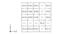
- the control processing device 54 first executes reference plate imaging processing (step S31). Thereby, the spectral spectrum concerning a reference board is imaged, and reference spectral image data A will be acquired (refer to Drawing 16).
- FIG. 16 is a schematic diagram showing the data structure of the reference spectral image data A two-dimensionally.
- a plurality of pixels are arranged in a matrix of m rows and n columns (1 ⁇ i ⁇ n, 1 ⁇ j ⁇ m, i, j, n and m are natural numbers), and each coordinate position (i, Each pixel j) has a predetermined luminance value data A (i, j).
- the column direction (longitudinal direction) is the wavelength dispersion direction (Y direction)
- the row direction (horizontal direction) is the imaging region width direction (X direction).
- step S32 the control processing unit 54 executes outlier removal processing (step S32).
- outlier removal process first of all, in the reference spectral image data A acquired in step S31, distribution is performed for each pixel row (the first to m-th rows) orthogonal to the wavelength dispersion direction (Y direction) of the spectral spectrum.
- the average ⁇ (j) and the standard deviation ⁇ (j) can be expressed by the following equation [Equation 1].
- ⁇ is a parameter.
- the average ⁇ ′ (i) and the standard deviation ⁇ ′ (i) can be expressed by the following relational expression [Equation 4].
- control processing device 54 executes a width direction-brightness characteristic acquisition process (step S33).
- This process corresponds to the imaging area luminance characteristic comprehension process in the present embodiment, and the imaging area luminance characteristic comprehension means in the present embodiment is configured by the processing function of the control processing device 54 that executes this process.
- outlier removal processing in step S32 causes the wavelength dispersion direction (Y direction) of the spectrum to be again determined with respect to the reference image data A (see FIG. 16) with outliers as invalid data.
- the distribution is determined for each of the pixel rows (first to m-th rows) orthogonal to.
- the mean ⁇ ′ ′ (j) and the standard deviation ⁇ ′ ′ (j) can be expressed by the following equation [Equation 5].
- Ch (j) is the number of data in the j-th pixel row.
- the average is normalized to 0 and the variance is normalized to 1 in the row direction.
- normalized data D which is two-dimensionally expanded as shown in FIG. 18 is obtained.
- the normalized data value D (i, j) related to each coordinate position (i, j) can be expressed by the following relational expression [Expression 6].
- an average value D ave (i) is obtained for each pixel row (first to n-th columns) in the normalized data D.
- the average value D ave (i) can be expressed by the following equation (7).
- Cv (i) is the number of data of the i-th pixel column.
- the ratio T (i) of the maximum to the minimum in the row direction is obtained.
- the ratio T (i) can be expressed by the following equation [Equation 8].
- the maximum value P max (i) and the minimum value P min (i) are determined for each pixel row (first to n-th columns) of the reference spectral image data A. Subsequently, the maximum value P max (i) at the position of the maximum value R max (i) in the row direction is determined, and the minimum value P min (i) at the position of the minimum value R min (i) in the row direction is determined.
- the ratio V (i) of row data obtained by this can be expressed by the following equation [Equation 9].
- the ratio V (i) of the row data is obtained as the width direction-brightness characteristic, and invalid data in the reference spectral image data A is obtained.
- the number Cx of all luminance value data removed and the sum Sumx of all luminance value data excluding the invalid data in the reference spectral image data A is acquired.
- the number Cx of all luminance value data excluding invalid data in the reference spectral image data A, and the total value Sumx of all luminance value data excluding invalid data in the reference spectral image data A are the relational expressions of the following [Equation 10] Can be represented by
- control processing unit 54 executes wavelength-sensitivity characteristic acquisition processing (step S34).
- This process corresponds to the wavelength sensitivity characteristic grasping process in the present embodiment, and the wavelength sensitivity characteristic grasping means in the present embodiment is constituted by the processing function of the control processing unit 54 which executes the process.
- outlier removal processing in step S32 is parallel to the wavelength dispersion direction (Y direction) of the spectral spectrum with respect to the reference image data A (see FIG. 16) with outliers as invalid data.
- the distribution is determined for each of the pixel columns (first to nth columns).
- the average ⁇ ′ ′ (i) and the standard deviation ⁇ ′ ′ (i) can be expressed by the following equation [Equation 11].
- Cv (i) is the number of data of the i-th pixel column.
- an average value D ave (j) is calculated for each pixel row (the first to m-th rows) in the normalized data D.
- the average value D ave (j) can be expressed by the following equation [Equation 13].
- Ch (j) is the number of data in the j-th pixel row.
- the maximum value R max (j) is normalized to 1 and the minimum value R min (j) is normalized to 0 with respect to the average value D ave (j).
- the ratio T (j) of the maximum to minimum in the column direction is obtained.
- the ratio T (j) can be expressed by the following equation [Equation 14].
- the maximum value P max (j) and the minimum value P min (j) are determined for each pixel row (first to m-th rows) of the reference spectral image data A. Subsequently, the maximum value P max (j) at the position of the maximum value R max (j) in the column direction is determined, and the minimum value P min (j) at the position of the minimum value R min (j) in the column direction is determined.
- the ratio V (j) of column data obtained by this can be expressed by the following equation [Equation 15].
- the ratio V (j) of the column data is acquired as the wavelength-sensitivity characteristic, and the invalid data is removed from the reference spectral image data A
- the total number Sumy of all luminance value data excluding the invalid data in the reference spectral image data A is acquired.
- step S35 the control processing device 54 executes a correction value calculation process.
- This process corresponds to the correction value calculation process in the present embodiment, and the correction value calculation means in the present embodiment is configured by the processing function of the control processing device 54 that executes this process.
- the ratio V (i) of row data acquired in step S33 and the ratio V (j) of column data acquired in step S34 are multiplied and expanded in two dimensions.
- a ratio (distribution) E of all luminance value data is obtained. That is, it is possible to acquire “width direction—wavelength-sensitivity characteristics in consideration of luminance characteristics (uneven luminance)” at each coordinate position.
- the ratio E (i, j) related to the coordinates (i, j) can be expressed by the following equation [Equation 17].
- an average value F ave of all luminance value data of the reference spectral image data A used to calculate the ratio V (i) of row data and the ratio V (j) of column data is obtained.
- the average value F ave can be expressed by the following equation [Equation 19].
- the luminance value data of the reference spectral image data A when the correction value becomes the Max value “1” is obtained.
- the Max value can be expressed by the following equation [Equation 20].
- the image data G after virtual correction as shown in FIG. 20 can be obtained by expanding this to the ratio E of all luminance value data shown in FIG.
- the luminance value data G (i, j) after correction relating to each coordinate (i, j) can be expressed by the following equation [Equation 21].
- the luminance value data G (i, j) after correction related to each coordinate (i, j) is divided by the luminance value data of the reference spectral image data A related to each coordinate (i, j), as shown in FIG.
- the correction value H (i, j) associated with each coordinate position (i, j) can be expressed by the following equation [Equation 22].
- the correction value H (i, j) relating to each coordinate position (i, j) obtained by the correction value calculation processing is stored in the setting data storage device 76 as storage means, and the correction value setting routine is ended. .
- the wavelength sensitivity characteristic of the imaging device 65 and the luminance characteristic of the imaging region are configured to be subjected to normalization processing, so that inspection accuracy is further increased as compared with the first embodiment. It can improve.
- the outlier removal process is performed, so that the inspection accuracy can be further improved.
- the content is the tablet 5
- the type, shape, and the like of the content are not particularly limited. It may be a supplement, food or the like. Tablets also include solid preparations such as uncoated tablets and sugar-coated tablets.
- the materials of the container film 3 and the cover film 4 are not limited to the above-described embodiments, and other materials may be adopted.
- the container film 3 may be formed of a metal material whose main material is aluminum, such as an aluminum laminated film.
- the arrangement and the number of the pocket portions 2 in the PTP sheet 1 are not limited to the above embodiments.
- various arrangements and numbers are available, including a type having 12 pockets in three rows. Can be adopted.
- the invention is not limited to this, and for example, in the post-process where the cover film 4 is attached to the container film 3 and the pre-process where the PTP sheet 1 is punched from the PTP film 6
- the configuration may be such that different-mixture inspection is performed.
- the different type mixture inspection by the inspection device 22 may be performed from the side of the container film 3 of the PTP sheet 1 conveyed by the pickup conveyor 39.
- the inspection apparatus 22 is provided with the inspection apparatus 22 as an apparatus for inspecting the PTP sheet 1 off-line separately from the PTP packing machine 10 instead of the configuration (inline) provided in the PTP packing machine 10 It is also good. Further, in such a case, the inspection device 22 may be provided with a transport unit capable of transporting the PTP sheet 1.
- the different-type mixture inspection by the inspection device 22 may be performed.
- the inspection may be performed before the tablet 5 is put into the tablet filling device 21. That is, apart from the PTP packaging machine 10, the inspection apparatus 22 may be provided as an apparatus for inspecting the tablets 5 off-line.
- the configurations of the illumination device 52 and the imaging device 53 are not limited to the above embodiments.
- a configuration may be adopted in which a reflection type diffraction grating, a prism, or the like is adopted as the spectroscopic means.
- spectral data is analyzed by principal component analysis (PCA).
- PCA principal component analysis
- the present invention is not limited to this, and other known methods such as PLS regression analysis may be used to analyze It is also good.
- the wavelength sensitivity characteristic of the imaging device 65 and the luminance characteristic of the imaging area are grasped, and the correction value is calculated based on these. Not limited to this, at least the wavelength sensitivity characteristic of the imaging device 65 may be grasped, and the correction value may be calculated based on this.
- the content of the wavelength-sensitivity characteristic acquisition processing and / or the content of the width direction-luminance characteristic acquisition processing is not limited to the content according to each of the above embodiments, and other configurations may be adopted. Good.
- the averaging process of averaging the luminance values of the pixels belonging to a predetermined pixel row or pixel column is performed, and the average luminance value calculated thereby is used as the characteristic of the pixel row or the pixel column.
- an addition process of adding the luminance values of pixels belonging to a predetermined pixel row or pixel column is performed, and the addition luminance value calculated by this is used as the pixel row or the pixel column It is good also as composition which makes it the characteristic concerning.
- the average is normalized to “0” as the first value
- the variance is normalized to “1” as the second value.
- the second value is not limited to “0” or “1”, and may be another value.
- the outlier removal process may be performed.
- the outlier removal process may be omitted.
Abstract
The purpose of the present invention is to provide an inspection device, a PTP packaging machine and a calibration method of the inspection device which can improve inspection accuracy related to inspection by using spectroscopic analysis. The inspection device 22 is provided with: a lighting device 52 which can irradiates a tablet 5 with near-infrared light; and an image capturing device 53 which can split reflection light reflected by the tablet 5 and capture an image, wherein analysis processing is performed on the basis of data of a spectroscopic image acquired by the image capturing device 53. The inspection device 22 executes a prescribed calculation process on reference spectroscopic image data acquired by capturing, in advance, an image of a spectrum related to a prescribed reference plate, and determines the wavelength sensitivity characteristics of an image capturing element by obtaining characteristics of each pixel row. Then, on the basis thereof, a correction value is calculated which corresponds to each pixel of the reference spectroscopic image data. At the time of inspection, each pixel's corresponding luminance value of acquired inspection spectroscopic image data, which is acquired by capturing an image of an object to be inspected, is corrected on the basis of the correction value corresponding to the pixel.
Description
本発明は、分光分析を利用して異品種の混入検査等を行う検査装置、及び、これを備えたPTP包装機、並びに、検査装置の較正方法に関するものである。
The present invention relates to an inspection apparatus that performs mixture inspection and the like of different varieties using spectral analysis, a PTP packaging machine provided with the same, and a calibration method of the inspection apparatus.
一般にPTPシートは、錠剤等の対象物が充填されるポケット部が形成された容器フィルムと、その容器フィルムに対しポケット部の開口側を密封するように取着されるカバーフィルムとから構成されている。
In general, a PTP sheet is composed of a container film having a pocket formed therein to be filled with an object such as a tablet, and a cover film attached to the container film so as to seal the open side of the pocket. There is.
PTPシートの製造に際しては、異品種の混入を検査する異品種混入検査などが行われる。かかる検査の手法として、従来、分光分析を利用した方法が知られている。
In the production of a PTP sheet, an examination of contamination of different varieties or the like for examining contamination of different varieties is performed. Conventionally, a method using spectral analysis is known as a method for such inspection.
かかる手法においては、例えば図22に示すように、PTPシートの製造過程において、容器フィルム81のポケット部82に充填された対象物83に対し、ハロゲンランプ等の光源から近赤外光L1を照射する。ここで、対象物83等から反射された反射光L2は、光学レンズ85により集光され、平行光L3となる。このうち、スリット86を通過した光は帯状のスリット光L4となり、分光手段としての分光器(プリズム)87に入射する。
In such a method, for example, as shown in FIG. 22, near infrared light L 1 is applied from a light source such as a halogen lamp to the target 83 filled in the pocket 82 of the container film 81 in the manufacturing process of the PTP sheet. Irradiate. Here, the reflected light L 2 reflected from the object 83, etc. is collected by the optical lens 85, it becomes parallel light L 3. Among these, the light passing through the slit 86 becomes a strip-like slit light L 4 , and enters into a spectroscope (prism) 87 as a spectroscope.
分光器87に入射したスリット光L4は、各波長成分の光に分光され、撮像素子88の受光面89に分光スペクトル(分光スペクトル像)L5として投射される。例えば1300nm~2000nmの波長帯域の近赤外光が1nm~10nm間隔の波長分解能で数十~数百バンドに分光される。
Slit light L 4 incident on the spectroscope 87 is dispersed into light of each wavelength component, the spectrum on the light receiving surface 89 of the image pickup device 88 (spectrum image) is projected as L 5. For example, near infrared light in a wavelength band of 1300 nm to 2000 nm is separated into several tens to several hundreds bands with wavelength resolution of 1 nm to 10 nm.
ここで、分光スペクトルL5の各波長成分は、その波長成分の違いにより、撮像素子88の受光面89上の異なる位置に投射される。そして、この分光スペクトルL5を撮像して得られるスペクトルデータを主成分分析することで異品種の混入を検出することができる。
Here, each wavelength component of the spectrum and L 5, the difference in wavelength components, is projected to different positions on the light receiving surface 89 of the image sensor 88. Then, it is possible to detect the contamination of different varieties spectral data obtained by imaging the spectrum L 5 by principal component analysis.
近年では、検査の高速化及び生産性の低下抑制を図るべく、CCDエリアセンサ等の撮像素子を用いて、搬送される容器フィルムの幅方向に一列に並ぶ複数のポケット部にそれぞれ充填される対象物を同時に検査可能な検査装置が提案されている(例えば、特許文献1参照)。
In recent years, in order to increase the speed of inspection and to suppress the decrease in productivity, an object to be filled in each of a plurality of pocket portions arranged in a line in the width direction of a conveyed container film using an imaging device such as a CCD area sensor An inspection apparatus capable of simultaneously inspecting an object has been proposed (see, for example, Patent Document 1).
CCDエリアセンサ等の撮像素子は、行列状に配列された複数の受光素子から構成されているため、個々の受光素子の特性に基づく感度のばらつきを補正する必要がある。
Since an imaging element such as a CCD area sensor is composed of a plurality of light receiving elements arranged in a matrix, it is necessary to correct variations in sensitivity based on the characteristics of the individual light receiving elements.
従来、受光素子の感度のばらつきを補正する方法としては、例えば強度が均一な光(均一光)を照射した基準板を撮像して得た画像データの各画素の輝度値を、全画素の平均輝度値で割り、該画素に対応する座標位置の感度値とし、検査時においては、取得した検査画像データの各画素の輝度値を該画素に係る感度値で割って補正する方法などが知られている(例えば、特許文献2の従来技術参照)。
Conventionally, as a method of correcting variations in sensitivity of the light receiving element, for example, the luminance value of each pixel of image data obtained by imaging a reference plate irradiated with light having uniform intensity (uniform light) is averaged over all pixels It is known to divide by the luminance value to obtain the sensitivity value of the coordinate position corresponding to the pixel, and to divide the luminance value of each pixel of the acquired inspection image data by the sensitivity value related to the pixel at the time of inspection. (See, for example, the prior art of Patent Document 2).
しかしながら、ハロゲンランプ等の光源から出射される近赤外光に含まれる各波長成分の強度は均一ではないため、分光スペクトルを撮像する場合においては、各波長成分によって撮像素子の感度が大きく変わることとなる。
However, since the intensity of each wavelength component contained in near-infrared light emitted from a light source such as a halogen lamp is not uniform, the sensitivity of the image pickup device largely changes depending on each wavelength component when imaging a spectral spectrum. It becomes.
そのため、仮に特許文献2の従来技術に記載されている技術と同様に、基準板を撮像して得た画像データの画素毎の輝度値をもとに、全画素の平均輝度値を画素毎の輝度値で割った値を該画素に対応する座標位置の補正値とした場合には、補正値の大きさも画素毎に大きく変わることになる。
Therefore, similarly to the technology described in the prior art of Patent Document 2, based on the luminance value of each pixel of the image data obtained by imaging the reference plate, the average luminance value of all pixels is calculated for each pixel. When the value divided by the luminance value is used as the correction value of the coordinate position corresponding to the pixel, the magnitude of the correction value also largely changes for each pixel.
かかる構成の下、検査時に取得した検査画像データの各画素の輝度値(計測値)に対し、該画素に係る補正値を掛けて、各画素の輝度値を補正した場合、補正値の大きい画素(例えば100)では、計測値に含まれるノイズが、補正値の小さい画素(例えば1)に対して大きくなる(例えば100倍大きくなる)。つまり、波長成分によってノイズレベルが大きく異なることとなる。結果として、適切なスペクトルデータを取得できず、検査精度が低下するおそれがある。
Under this configuration, when the luminance value of each pixel is corrected by multiplying the luminance value (measurement value) of each pixel of the inspection image data acquired at the time of inspection by the correction value related to the pixel, a pixel having a large correction value At (for example, 100), the noise included in the measurement value is larger (for example, 100 times larger) with respect to the pixel (for example, 1) having a smaller correction value. That is, the noise level is largely different depending on the wavelength component. As a result, appropriate spectral data can not be obtained, which may reduce inspection accuracy.
従って、分光分析を利用した検査を行う場合においては、個々の受光素子の特性のみならず、波長成分の違いを考慮して感度のばらつきを補正する必要がある。
Therefore, when performing inspection using spectral analysis, it is necessary to correct the variation in sensitivity in consideration of not only the characteristics of individual light receiving elements but also the difference in wavelength components.
本発明は、上記事情に鑑みてなされたものであり、その目的は、分光分析を利用した検査に係る検査精度の向上を図ることのできる検査装置、PTP包装機及び検査装置の較正方法を提供することにある。
The present invention has been made in view of the above circumstances, and an object thereof is to provide an inspection device, a PTP packaging machine, and a calibration method of the inspection device capable of improving the inspection accuracy relating to an inspection using spectral analysis. It is to do.
以下、上記課題を解決するのに適した各手段につき項分けして説明する。なお、必要に応じて対応する手段に特有の作用効果を付記する。
Hereinafter, each means suitable for solving the above-mentioned subject will be described by item. In addition, the operation and effect specific to the corresponding means will be added as needed.
手段1.対象物に対し近赤外光を照射可能な照射手段と、
前記近赤外光が照射された前記対象物から反射される反射光を分光可能な分光手段と、
複数の受光素子が行列状に配置された撮像素子を有し、前記分光手段にて分光された前記反射光に係る分光スペクトルを撮像可能な撮像手段とを備え、
前記撮像手段により取得された分光画像データを基に、分光分析を利用して所定の検査(例えば異品種混入検査)を行う検査装置であって、
前記撮像手段により所定の基準対象物(例えば基準板)に係る分光スペクトルを撮像し取得した基準分光画像データにおける、前記分光スペクトルの波長分散方向と直交する各画素行及び/又は前記波長分散方向と平行する各画素列それぞれについて、該画素行又は該画素列に属する画素(一部又は全部の画素)の輝度値を用いて所定の演算処理(例えば加算処理、平均処理、正規化処理など)を実行し、各画素行毎の特性を求めることにより、前記照射手段から照射される近赤外光の下での前記撮像素子の波長感度特性を把握する波長感度特性把握手段と、
前記基準分光画像データの各画素の輝度値、及び、該画素が属する画素行に係る前記特性を基に、前記基準分光画像データの各画素に対応する座標位置それぞれに係る補正値を算出する補正値算出手段と、
前記撮像手段により所定の検査対象物(例えば錠剤)を撮像し取得した検査分光画像データの各画素の輝度値を、該画素に対応する座標位置に係る前記補正値を基に補正する画像補正手段と、
前記検査分光画像データを補正した補正分光画像データを基にスペクトルデータを取得可能なスペクトルデータ取得手段と、
前記スペクトルデータを基に、前記検査対象物について所定の分析処理(例えば主成分分析)を行う分析手段とを備えたことを特徴とする検査装置。Means 1. An irradiation unit capable of irradiating near infrared light to the object;
Spectroscopic means capable of dispersing the reflected light reflected from the object irradiated with the near infrared light;
The imaging device includes: an imaging device in which a plurality of light receiving devices are arranged in a matrix; and an imaging device capable of imaging a spectrum relating to the reflected light dispersed by the dispersing device;
An inspection apparatus for performing a predetermined inspection (for example, different-mixture inspection) using spectral analysis based on spectral image data acquired by the imaging unit,
Each pixel row orthogonal to the wavelength dispersion direction of the spectral spectrum and / or the wavelength dispersion direction in reference spectral image data obtained by imaging the spectral spectrum of a predetermined reference object (for example, a reference plate) by the imaging means and acquired For each parallel pixel row, predetermined arithmetic processing (for example, addition processing, averaging processing, normalization processing, etc.) is performed using the luminance value of the pixel row or pixels (part or all of the pixels) belonging to the pixel row Wavelength sensitivity characteristic grasping means for grasping the wavelength sensitivity characteristic of the image pickup device under near infrared light emitted from the irradiating means by performing the process and obtaining the characteristic for each pixel row;
Based on the luminance value of each pixel of the reference spectral image data and the characteristics of the pixel row to which the pixel belongs, a correction value is calculated for each coordinate position corresponding to each pixel of the reference spectral image data Value calculation means,
Image correction means for correcting the luminance value of each pixel of the inspection spectral image data acquired by imaging a predetermined inspection object (for example, a tablet) by the imaging means based on the correction value associated with the coordinate position corresponding to the pixel When,
Spectrum data acquisition means capable of acquiring spectrum data based on the corrected spectral image data obtained by correcting the inspection spectral image data;
An inspection apparatus comprising: analysis means for performing predetermined analysis processing (for example, principal component analysis) on the inspection object based on the spectrum data.
前記近赤外光が照射された前記対象物から反射される反射光を分光可能な分光手段と、
複数の受光素子が行列状に配置された撮像素子を有し、前記分光手段にて分光された前記反射光に係る分光スペクトルを撮像可能な撮像手段とを備え、
前記撮像手段により取得された分光画像データを基に、分光分析を利用して所定の検査(例えば異品種混入検査)を行う検査装置であって、
前記撮像手段により所定の基準対象物(例えば基準板)に係る分光スペクトルを撮像し取得した基準分光画像データにおける、前記分光スペクトルの波長分散方向と直交する各画素行及び/又は前記波長分散方向と平行する各画素列それぞれについて、該画素行又は該画素列に属する画素(一部又は全部の画素)の輝度値を用いて所定の演算処理(例えば加算処理、平均処理、正規化処理など)を実行し、各画素行毎の特性を求めることにより、前記照射手段から照射される近赤外光の下での前記撮像素子の波長感度特性を把握する波長感度特性把握手段と、
前記基準分光画像データの各画素の輝度値、及び、該画素が属する画素行に係る前記特性を基に、前記基準分光画像データの各画素に対応する座標位置それぞれに係る補正値を算出する補正値算出手段と、
前記撮像手段により所定の検査対象物(例えば錠剤)を撮像し取得した検査分光画像データの各画素の輝度値を、該画素に対応する座標位置に係る前記補正値を基に補正する画像補正手段と、
前記検査分光画像データを補正した補正分光画像データを基にスペクトルデータを取得可能なスペクトルデータ取得手段と、
前記スペクトルデータを基に、前記検査対象物について所定の分析処理(例えば主成分分析)を行う分析手段とを備えたことを特徴とする検査装置。
Spectroscopic means capable of dispersing the reflected light reflected from the object irradiated with the near infrared light;
The imaging device includes: an imaging device in which a plurality of light receiving devices are arranged in a matrix; and an imaging device capable of imaging a spectrum relating to the reflected light dispersed by the dispersing device;
An inspection apparatus for performing a predetermined inspection (for example, different-mixture inspection) using spectral analysis based on spectral image data acquired by the imaging unit,
Each pixel row orthogonal to the wavelength dispersion direction of the spectral spectrum and / or the wavelength dispersion direction in reference spectral image data obtained by imaging the spectral spectrum of a predetermined reference object (for example, a reference plate) by the imaging means and acquired For each parallel pixel row, predetermined arithmetic processing (for example, addition processing, averaging processing, normalization processing, etc.) is performed using the luminance value of the pixel row or pixels (part or all of the pixels) belonging to the pixel row Wavelength sensitivity characteristic grasping means for grasping the wavelength sensitivity characteristic of the image pickup device under near infrared light emitted from the irradiating means by performing the process and obtaining the characteristic for each pixel row;
Based on the luminance value of each pixel of the reference spectral image data and the characteristics of the pixel row to which the pixel belongs, a correction value is calculated for each coordinate position corresponding to each pixel of the reference spectral image data Value calculation means,
Image correction means for correcting the luminance value of each pixel of the inspection spectral image data acquired by imaging a predetermined inspection object (for example, a tablet) by the imaging means based on the correction value associated with the coordinate position corresponding to the pixel When,
Spectrum data acquisition means capable of acquiring spectrum data based on the corrected spectral image data obtained by correcting the inspection spectral image data;
An inspection apparatus comprising: analysis means for performing predetermined analysis processing (for example, principal component analysis) on the inspection object based on the spectrum data.
上記手段1によれば、基準分光画像データに対し所定の演算処理を実行し、各画素行毎(各波長成分毎)の特性を求めることにより、撮像素子の平均的な波長感度特性を把握することができる。
According to the above means 1, the average wavelength sensitivity characteristic of the image pickup device is grasped by executing predetermined arithmetic processing on the reference spectral image data and obtaining the characteristic of each pixel row (each wavelength component). be able to.
そして、基準分光画像データの各画素の輝度値、及び、該画素が属する画素行に係る特性(波長感度特性)を基に、基準分光画像データの各画素に対応する座標位置それぞれに係る補正値を算出する構成となっている。
Then, based on the luminance value of each pixel of the reference spectral image data and the characteristic (wavelength sensitivity characteristic) of the pixel row to which the pixel belongs, a correction value concerning each coordinate position corresponding to each pixel of the reference spectral image data Is calculated.
このため、補正値の大きさが画素毎に極端に変わらず、波長成分によってノイズレベルが大きく異なってしまうような不具合の発生を抑制することができる。結果として、分光分析を利用した検査に係る検査精度の向上を図ることができる。
For this reason, the magnitude of the correction value does not change extremely for each pixel, and it is possible to suppress the occurrence of a defect in which the noise level largely differs depending on the wavelength component. As a result, it is possible to improve the inspection accuracy according to the inspection using spectral analysis.
尚、撮像手段(受光素子)の出力レベルは、環境変化や温度変化、光源の違い等に伴い変化するため、検査装置の製造時において適切な補正値を事前に設定しておくことは難しい。
Since the output level of the imaging means (light receiving element) changes with environmental changes, temperature changes, differences in light sources, etc., it is difficult to set in advance an appropriate correction value at the time of manufacturing the inspection apparatus.
手段2.対象物に対し近赤外光を照射可能な照射手段と、
前記近赤外光が照射された前記対象物から反射される反射光を分光可能な分光手段と、
複数の受光素子が行列状に配置された撮像素子を有し、前記分光手段にて分光された前記反射光に係る分光スペクトルを撮像可能な撮像手段とを備え、
前記撮像手段により取得された分光画像データを基に、分光分析を利用して所定の検査(例えば異品種混入検査)を行う検査装置であって、
前記撮像手段により所定の基準対象物(例えば基準板)に係る分光スペクトルを撮像し取得した基準分光画像データにおける、前記分光スペクトルの波長分散方向と直交する各画素行及び/又は前記波長分散方向と平行する各画素列それぞれについて、該画素行又は該画素列に属する画素(一部又は全部の画素)の輝度値を用いて所定の演算処理(例えば加算処理、平均処理、正規化処理など)を実行し、各画素行毎の特性を求めることにより、前記照射手段から照射される近赤外光の下での前記撮像素子の波長感度特性を把握する波長感度特性把握手段と、
前記基準分光画像データにおける、前記波長分散方向と平行する各画素列及び/又は前記波長分散方向と直交する各画素行それぞれについて、該画素列又は該画素行に属する画素(一部又は全部の画素)の輝度値を用いて所定の演算処理(例えば加算処理、平均処理、正規化処理など)を実行し、各画素列毎の特性を求めることにより、前記照射手段から照射される近赤外光の下での撮像領域の輝度特性(例えば照射光の輝度ムラ)を把握する撮像領域輝度特性把握手段と、
前記基準分光画像データの各画素の輝度値、並びに、該画素が属する画素行に係る前記特性、及び、該画素が属する画素列に係る前記特性を基に、前記基準分光画像データの各画素に対応する座標位置それぞれに係る補正値を算出する補正値算出手段と、
前記撮像手段により所定の検査対象物(例えば錠剤)を撮像し取得した検査分光画像データの各画素の輝度値を、該画素に対応する座標位置に係る前記補正値を基に補正する画像補正手段と、
前記検査分光画像データを補正した補正分光画像データを基にスペクトルデータを取得可能なスペクトルデータ取得手段と、
前記スペクトルデータを基に、前記検査対象物について所定の分析処理(例えば主成分分析)を行う分析手段とを備えたことを特徴とする検査装置。Means 2. An irradiation unit capable of irradiating near infrared light to the object;
Spectroscopic means capable of dispersing the reflected light reflected from the object irradiated with the near infrared light;
The imaging device includes: an imaging device in which a plurality of light receiving devices are arranged in a matrix; and an imaging device capable of imaging a spectrum relating to the reflected light dispersed by the dispersing device;
An inspection apparatus for performing a predetermined inspection (for example, different-mixture inspection) using spectral analysis based on spectral image data acquired by the imaging unit,
Each pixel row orthogonal to the wavelength dispersion direction of the spectral spectrum and / or the wavelength dispersion direction in reference spectral image data obtained by imaging the spectral spectrum of a predetermined reference object (for example, a reference plate) by the imaging means and acquired For each parallel pixel row, predetermined arithmetic processing (for example, addition processing, averaging processing, normalization processing, etc.) is performed using the luminance value of the pixel row or pixels (part or all of the pixels) belonging to the pixel row Wavelength sensitivity characteristic grasping means for grasping the wavelength sensitivity characteristic of the image pickup device under near infrared light emitted from the irradiating means by performing the process and obtaining the characteristic for each pixel row;
For each pixel row parallel to the wavelength dispersion direction and / or each pixel row orthogonal to the wavelength dispersion direction in the reference spectral image data, pixels (part or all pixels belonging to the pixel row or the pixel row) Near infrared light irradiated from the irradiation unit by performing predetermined arithmetic processing (for example, addition processing, averaging processing, normalization processing, etc.) using the luminance value of An imaging area luminance characteristic grasping means for grasping the luminance characteristic (for example, the luminance unevenness of the irradiation light) of the imaging area under the image;
On each pixel of the reference spectral image data, based on the luminance value of each pixel of the reference spectral image data, the characteristic of the pixel row to which the pixel belongs, and the characteristic of the pixel column to which the pixel belongs Correction value calculation means for calculating a correction value associated with each corresponding coordinate position;
Image correction means for correcting the luminance value of each pixel of the inspection spectral image data acquired by imaging a predetermined inspection object (for example, a tablet) by the imaging means based on the correction value associated with the coordinate position corresponding to the pixel When,
Spectrum data acquisition means capable of acquiring spectrum data based on the corrected spectral image data obtained by correcting the inspection spectral image data;
An inspection apparatus comprising: analysis means for performing predetermined analysis processing (for example, principal component analysis) on the inspection object based on the spectrum data.
前記近赤外光が照射された前記対象物から反射される反射光を分光可能な分光手段と、
複数の受光素子が行列状に配置された撮像素子を有し、前記分光手段にて分光された前記反射光に係る分光スペクトルを撮像可能な撮像手段とを備え、
前記撮像手段により取得された分光画像データを基に、分光分析を利用して所定の検査(例えば異品種混入検査)を行う検査装置であって、
前記撮像手段により所定の基準対象物(例えば基準板)に係る分光スペクトルを撮像し取得した基準分光画像データにおける、前記分光スペクトルの波長分散方向と直交する各画素行及び/又は前記波長分散方向と平行する各画素列それぞれについて、該画素行又は該画素列に属する画素(一部又は全部の画素)の輝度値を用いて所定の演算処理(例えば加算処理、平均処理、正規化処理など)を実行し、各画素行毎の特性を求めることにより、前記照射手段から照射される近赤外光の下での前記撮像素子の波長感度特性を把握する波長感度特性把握手段と、
前記基準分光画像データにおける、前記波長分散方向と平行する各画素列及び/又は前記波長分散方向と直交する各画素行それぞれについて、該画素列又は該画素行に属する画素(一部又は全部の画素)の輝度値を用いて所定の演算処理(例えば加算処理、平均処理、正規化処理など)を実行し、各画素列毎の特性を求めることにより、前記照射手段から照射される近赤外光の下での撮像領域の輝度特性(例えば照射光の輝度ムラ)を把握する撮像領域輝度特性把握手段と、
前記基準分光画像データの各画素の輝度値、並びに、該画素が属する画素行に係る前記特性、及び、該画素が属する画素列に係る前記特性を基に、前記基準分光画像データの各画素に対応する座標位置それぞれに係る補正値を算出する補正値算出手段と、
前記撮像手段により所定の検査対象物(例えば錠剤)を撮像し取得した検査分光画像データの各画素の輝度値を、該画素に対応する座標位置に係る前記補正値を基に補正する画像補正手段と、
前記検査分光画像データを補正した補正分光画像データを基にスペクトルデータを取得可能なスペクトルデータ取得手段と、
前記スペクトルデータを基に、前記検査対象物について所定の分析処理(例えば主成分分析)を行う分析手段とを備えたことを特徴とする検査装置。
Spectroscopic means capable of dispersing the reflected light reflected from the object irradiated with the near infrared light;
The imaging device includes: an imaging device in which a plurality of light receiving devices are arranged in a matrix; and an imaging device capable of imaging a spectrum relating to the reflected light dispersed by the dispersing device;
An inspection apparatus for performing a predetermined inspection (for example, different-mixture inspection) using spectral analysis based on spectral image data acquired by the imaging unit,
Each pixel row orthogonal to the wavelength dispersion direction of the spectral spectrum and / or the wavelength dispersion direction in reference spectral image data obtained by imaging the spectral spectrum of a predetermined reference object (for example, a reference plate) by the imaging means and acquired For each parallel pixel row, predetermined arithmetic processing (for example, addition processing, averaging processing, normalization processing, etc.) is performed using the luminance value of the pixel row or pixels (part or all of the pixels) belonging to the pixel row Wavelength sensitivity characteristic grasping means for grasping the wavelength sensitivity characteristic of the image pickup device under near infrared light emitted from the irradiating means by performing the process and obtaining the characteristic for each pixel row;
For each pixel row parallel to the wavelength dispersion direction and / or each pixel row orthogonal to the wavelength dispersion direction in the reference spectral image data, pixels (part or all pixels belonging to the pixel row or the pixel row) Near infrared light irradiated from the irradiation unit by performing predetermined arithmetic processing (for example, addition processing, averaging processing, normalization processing, etc.) using the luminance value of An imaging area luminance characteristic grasping means for grasping the luminance characteristic (for example, the luminance unevenness of the irradiation light) of the imaging area under the image;
On each pixel of the reference spectral image data, based on the luminance value of each pixel of the reference spectral image data, the characteristic of the pixel row to which the pixel belongs, and the characteristic of the pixel column to which the pixel belongs Correction value calculation means for calculating a correction value associated with each corresponding coordinate position;
Image correction means for correcting the luminance value of each pixel of the inspection spectral image data acquired by imaging a predetermined inspection object (for example, a tablet) by the imaging means based on the correction value associated with the coordinate position corresponding to the pixel When,
Spectrum data acquisition means capable of acquiring spectrum data based on the corrected spectral image data obtained by correcting the inspection spectral image data;
An inspection apparatus comprising: analysis means for performing predetermined analysis processing (for example, principal component analysis) on the inspection object based on the spectrum data.
上記手段2によれば、基準分光画像データに対し所定の演算処理を実行し、各画素行毎(各波長成分毎)の特性を求めることにより、撮像素子の平均的な波長感度特性を把握することができる。
According to the above means 2, the average wavelength sensitivity characteristic of the image pickup device is grasped by executing predetermined arithmetic processing on the reference spectral image data and obtaining the characteristic for each pixel row (for each wavelength component). be able to.
加えて、基準分光画像データに対し所定の演算処理を実行し、各画素列毎(波長分散方向と直交する撮像領域幅方向における各座標位置毎)の特性を求めることにより、撮像領域幅方向における平均的な輝度特性を把握することができる。
In addition, predetermined arithmetic processing is performed on the reference spectral image data to obtain characteristics of each pixel row (each coordinate position in the imaging region width direction orthogonal to the wavelength dispersion direction), thereby obtaining the imaging region width direction. Average brightness characteristics can be grasped.
そして、基準分光画像データの各画素の輝度値、並びに、該画素が属する画素行に係る特性(波長感度特性)、及び、該画素が属する画素列に係る特性(撮像領域輝度特性)を基に、基準分光画像データの各画素に対応する座標位置それぞれに係る補正値を算出する構成となっている。
Then, based on the luminance value of each pixel of the reference spectral image data, the characteristic related to the pixel row to which the pixel belongs (wavelength sensitivity characteristic), and the characteristic related to the pixel column to which the pixel belongs (imaging area luminance characteristic) Correction values relating to each of the coordinate positions corresponding to each pixel of the reference spectral image data are calculated.
このため、本手段2によれば、上記手段1の作用効果に加え、補正値のノイズレベルが撮像領域の座標位置による輝度ムラの影響を受けにくくなる。結果として、分光分析を利用した検査に係る検査精度のさらなる向上を図ることができる。
For this reason, according to this means 2, in addition to the effects of the above means 1, the noise level of the correction value is less likely to be affected by uneven brightness due to the coordinate position of the imaging region. As a result, it is possible to further improve the inspection accuracy according to the inspection using spectral analysis.
例えば停止した対象物から反射される反射光の分光スペクトルを撮像する場合であれば、特許文献2に記載されたラインセンサを走査する技術を利用して、個々の受光素子の特性に基づく感度のばらつきを軽減することは可能となる。
For example, in the case of imaging the spectrum of the reflected light reflected from the stopped object, using the technique of scanning the line sensor described in Patent Document 2, sensitivity based on the characteristics of the individual light receiving elements It is possible to reduce the variation.
しかしながら、撮像領域の各座標位置(分光分析の分野においては、分光スペクトルの波長分散方向と直交する撮像領域幅方向における各座標位置)に対して強度が均一な光を照射することは困難であるため、均一光を照射して補正値を得たとしても、各座標位置に係る感度のばらつきを正確に補正することは難しい。
However, it is difficult to irradiate light with uniform intensity to each coordinate position of the imaging region (in the field of spectral analysis, each coordinate position in the imaging region width direction orthogonal to the wavelength dispersion direction of the spectral spectrum) Therefore, even if uniform light is irradiated to obtain a correction value, it is difficult to accurately correct the variation in sensitivity related to each coordinate position.
また、センサを走査する技術は、検査装置の構造を複雑化するだけでなく、検査に多大な時間を要するおそれがある。
Moreover, the technique of scanning the sensor not only complicates the structure of the inspection apparatus, but also may require a large amount of time for inspection.
近年、PTPシートの製造分野などにおいては、生産速度の高速化に伴い、異品種混入検査など各種検査の高速化が求められている。例えばPTP包装機上で検査を行う場合には、1秒当たり100個以上の対象物を検査することが求められる場合もある。このため、特許文献2に係る技術等はPTP包装機上での検査には適さない。
In recent years, in the field of manufacturing PTP sheets and the like, speeding up of various types of inspection such as inspection of mixing of different types has been required along with speeding up of production speed. For example, when performing inspection on a PTP packaging machine, it may be required to inspect 100 or more objects per second. For this reason, the technique etc. which concern on patent document 2 are not suitable for the test | inspection on a PTP packaging machine.
手段3.容器フィルムに形成されたポケット部に所定の内容物が収容され、該ポケット部を塞ぐようにカバーフィルムが取着されてなるPTPシートを製造するためのPTP包装機であって、
帯状に搬送される前記容器フィルムに対し前記ポケット部を形成するポケット部形成手段と、
前記ポケット部に前記内容物を充填する充填手段と、
前記ポケット部に前記内容物が充填された前記容器フィルムに対し、前記ポケット部を塞ぐようにして帯状の前記カバーフィルムを取着する取着手段と、
前記容器フィルムに前記カバーフィルムが取着された帯状体(帯状のPTPフィルム)から前記PTPシートを切離す切離手段(シート単位に打抜く打抜手段を含む)と、
前記内容物を前記検査対象物として検査を行う上記手段1又は2に記載の検査装置とを備えたことを特徴とするPTP包装機。Means 3. A PTP packaging machine for producing a PTP sheet in which a predetermined content is accommodated in a pocket portion formed in a container film, and a cover film is attached so as to close the pocket portion,
Pocket portion forming means for forming the pocket portion with respect to the container film conveyed in a belt shape;
Filling means for filling the contents in the pocket portion;
An attachment means for attaching the strip-like cover film so as to close the pocket portion to the container film in which the content is filled in the pocket portion;
Separating means (including punching means for punching sheet units) for separating the PTP sheet from a strip (band-like PTP film) in which the cover film is attached to the container film;
A PTP packing machine comprising: the inspection device according to the above-mentioned means 1 or 2 which inspects the contents as the inspection object.
帯状に搬送される前記容器フィルムに対し前記ポケット部を形成するポケット部形成手段と、
前記ポケット部に前記内容物を充填する充填手段と、
前記ポケット部に前記内容物が充填された前記容器フィルムに対し、前記ポケット部を塞ぐようにして帯状の前記カバーフィルムを取着する取着手段と、
前記容器フィルムに前記カバーフィルムが取着された帯状体(帯状のPTPフィルム)から前記PTPシートを切離す切離手段(シート単位に打抜く打抜手段を含む)と、
前記内容物を前記検査対象物として検査を行う上記手段1又は2に記載の検査装置とを備えたことを特徴とするPTP包装機。
Pocket portion forming means for forming the pocket portion with respect to the container film conveyed in a belt shape;
Filling means for filling the contents in the pocket portion;
An attachment means for attaching the strip-like cover film so as to close the pocket portion to the container film in which the content is filled in the pocket portion;
Separating means (including punching means for punching sheet units) for separating the PTP sheet from a strip (band-like PTP film) in which the cover film is attached to the container film;
A PTP packing machine comprising: the inspection device according to the above-mentioned
上記手段3のように、上記手段1等に係る検査装置をPTP包装機に備えることで、PTPシートの製造過程において異品種を含む不良品を効率的に除外できる等のメリットが生じる。また、PTP包装機は、上記検査装置によって不良と判定されたPTPシートを排出する排出手段を備える構成としてもよい。
By providing the inspection apparatus according to the above means 1 etc. in the PTP packaging machine as in the above means 3, merits arise such that defective products including different types can be efficiently excluded in the manufacturing process of the PTP sheet. In addition, the PTP packaging machine may be configured to include a discharge unit that discharges the PTP sheet determined to be defective by the inspection device.
尚、上記手段3において、上記検査装置を「充填手段によりポケット部に内容物(検査対象物)が充填される前工程」に配置した構成としてもよい。かかる場合、ポケット部に充填される前段階に異品種を排除することが可能となり、不良品となるPTPシートを低減することができる。
In the means 3, the inspection apparatus may be arranged as "a pre-process in which the contents (inspection object) are filled in the pocket portion by the filling means". In such a case, it is possible to eliminate different varieties before filling into the pocket, and to reduce the number of defective PTP sheets.
また、上記検査装置を「充填手段によりポケット部に内容物(検査対象物)が充填された後工程かつ取着手段によりカバーフィルムが取着される前工程」に配置した構成としてもよい。かかる場合、内容物(検査対象物)を遮るものがない状態で検査を実行することができ、さらなる検査精度の向上を図ることができる。
In addition, the inspection apparatus may be arranged in "the process after the contents (the object to be inspected) are filled in the pocket by the filling means and the process before the cover film is attached by the attaching means". In such a case, the inspection can be performed without interrupting the contents (object to be inspected), and the inspection accuracy can be further improved.
また、上記検査装置を「取着手段によりカバーフィルムが取着された後工程かつ切離手段によりPTPシートが切離される前工程」に配置した構成としてもよい。かかる場合、内容物(検査対象物)が入れ替わることがない状態で検査を実行することができ、さらなる検査精度の向上を図ることができる。
In addition, the inspection apparatus may be arranged in "the process after the cover film is attached by the attaching means and the process before the PTP sheet is detached by the detaching means". In such a case, the inspection can be performed in a state in which the contents (inspection object) are not replaced, and the inspection accuracy can be further improved.
また、上記検査装置を「切離手段によりPTPシートが切離された後工程」に配置した構成としてもよい。かかる場合、不良品が混ざっていないかを最終段階で確認することができる。
In addition, the inspection apparatus may be disposed in the “process after the PTP sheet is separated by the separation unit”. In such a case, it can be confirmed at the final stage whether or not defective products are mixed.
手段4.対象物に対し近赤外光を照射可能な照射手段と、
前記近赤外光が照射された前記対象物から反射される反射光を分光可能な分光手段と、
複数の受光素子が行列状に配置された撮像素子を有し、前記分光手段にて分光された前記反射光に係る分光スペクトルを撮像可能な撮像手段とを備え、
前記撮像手段により取得された分光画像データを基に、分光分析を利用して所定の検査(例えば異品種混入検査)を行う検査装置の較正方法であって、
前記撮像手段により所定の基準対象物(例えば基準板)に係る分光スペクトルを撮像し取得した基準分光画像データにおける、前記分光スペクトルの波長分散方向と直交する各画素行及び/又は前記波長分散方向と平行する各画素列それぞれについて、該画素行又は該画素列に属する画素(一部又は全部の画素)の輝度値を用いて所定の演算処理(例えば加算処理、平均処理、正規化処理など)を実行し、各画素行毎の特性を求めることにより、前記照射手段から照射される近赤外光の下での前記撮像素子の波長感度特性を把握する波長感度特性把握工程と、
前記基準分光画像データの各画素の輝度値、及び、該画素が属する画素行に係る前記特性を基に、前記基準分光画像データの各画素に対応する座標位置それぞれに係る補正値を算出する補正値算出工程と、
前記撮像手段により所定の検査対象物(例えば錠剤)を撮像し取得した検査分光画像データの各画素の輝度値を、該画素に対応する座標位置に係る前記補正値を基に補正する画像補正工程とを備えたことを特徴とする検査装置の較正方法。Means 4. An irradiation unit capable of irradiating near infrared light to the object;
Spectroscopic means capable of dispersing the reflected light reflected from the object irradiated with the near infrared light;
The imaging device includes: an imaging device in which a plurality of light receiving devices are arranged in a matrix; and an imaging device capable of imaging a spectrum relating to the reflected light dispersed by the dispersing device;
It is a calibration method of an inspection apparatus which performs predetermined inspection (for example, different-mixture inspection) using spectral analysis based on spectral image data acquired by the imaging means,
Each pixel row orthogonal to the wavelength dispersion direction of the spectral spectrum and / or the wavelength dispersion direction in reference spectral image data obtained by imaging the spectral spectrum of a predetermined reference object (for example, a reference plate) by the imaging means and acquired For each parallel pixel row, predetermined arithmetic processing (for example, addition processing, averaging processing, normalization processing, etc.) is performed using the luminance value of the pixel row or pixels (part or all of the pixels) belonging to the pixel row A wavelength sensitivity characteristic grasping step of grasping the wavelength sensitivity characteristic of the image pickup device under near infrared light emitted from the irradiating unit by performing the process and determining the characteristic of each pixel row;
Based on the luminance value of each pixel of the reference spectral image data and the characteristics of the pixel row to which the pixel belongs, a correction value is calculated for each coordinate position corresponding to each pixel of the reference spectral image data Value calculation process,
An image correction step of correcting a luminance value of each pixel of inspection spectral image data acquired by imaging a predetermined inspection object (for example, a tablet) by the imaging unit and based on the correction value at a coordinate position corresponding to the pixel And a calibration method of the inspection apparatus.
前記近赤外光が照射された前記対象物から反射される反射光を分光可能な分光手段と、
複数の受光素子が行列状に配置された撮像素子を有し、前記分光手段にて分光された前記反射光に係る分光スペクトルを撮像可能な撮像手段とを備え、
前記撮像手段により取得された分光画像データを基に、分光分析を利用して所定の検査(例えば異品種混入検査)を行う検査装置の較正方法であって、
前記撮像手段により所定の基準対象物(例えば基準板)に係る分光スペクトルを撮像し取得した基準分光画像データにおける、前記分光スペクトルの波長分散方向と直交する各画素行及び/又は前記波長分散方向と平行する各画素列それぞれについて、該画素行又は該画素列に属する画素(一部又は全部の画素)の輝度値を用いて所定の演算処理(例えば加算処理、平均処理、正規化処理など)を実行し、各画素行毎の特性を求めることにより、前記照射手段から照射される近赤外光の下での前記撮像素子の波長感度特性を把握する波長感度特性把握工程と、
前記基準分光画像データの各画素の輝度値、及び、該画素が属する画素行に係る前記特性を基に、前記基準分光画像データの各画素に対応する座標位置それぞれに係る補正値を算出する補正値算出工程と、
前記撮像手段により所定の検査対象物(例えば錠剤)を撮像し取得した検査分光画像データの各画素の輝度値を、該画素に対応する座標位置に係る前記補正値を基に補正する画像補正工程とを備えたことを特徴とする検査装置の較正方法。
Spectroscopic means capable of dispersing the reflected light reflected from the object irradiated with the near infrared light;
The imaging device includes: an imaging device in which a plurality of light receiving devices are arranged in a matrix; and an imaging device capable of imaging a spectrum relating to the reflected light dispersed by the dispersing device;
It is a calibration method of an inspection apparatus which performs predetermined inspection (for example, different-mixture inspection) using spectral analysis based on spectral image data acquired by the imaging means,
Each pixel row orthogonal to the wavelength dispersion direction of the spectral spectrum and / or the wavelength dispersion direction in reference spectral image data obtained by imaging the spectral spectrum of a predetermined reference object (for example, a reference plate) by the imaging means and acquired For each parallel pixel row, predetermined arithmetic processing (for example, addition processing, averaging processing, normalization processing, etc.) is performed using the luminance value of the pixel row or pixels (part or all of the pixels) belonging to the pixel row A wavelength sensitivity characteristic grasping step of grasping the wavelength sensitivity characteristic of the image pickup device under near infrared light emitted from the irradiating unit by performing the process and determining the characteristic of each pixel row;
Based on the luminance value of each pixel of the reference spectral image data and the characteristics of the pixel row to which the pixel belongs, a correction value is calculated for each coordinate position corresponding to each pixel of the reference spectral image data Value calculation process,
An image correction step of correcting a luminance value of each pixel of inspection spectral image data acquired by imaging a predetermined inspection object (for example, a tablet) by the imaging unit and based on the correction value at a coordinate position corresponding to the pixel And a calibration method of the inspection apparatus.
上記手段4によれば、上記手段1と同様の作用効果が奏されることとなる。
According to the above-mentioned means 4, the same operation and effect as the above-mentioned means 1 will be exerted.
手段5.対象物に対し近赤外光を照射可能な照射手段と、
前記近赤外光が照射された前記対象物から反射される反射光を分光可能な分光手段と、
複数の受光素子が行列状に配置された撮像素子を有し、前記分光手段にて分光された前記反射光に係る分光スペクトルを撮像可能な撮像手段とを備え、
前記撮像手段により取得された分光画像データを基に、分光分析を利用して所定の検査(例えば異品種混入検査)を行う検査装置の較正方法であって、
前記撮像手段により所定の基準対象物(例えば基準板)に係る分光スペクトルを撮像し取得した基準分光画像データにおける、前記分光スペクトルの波長分散方向と直交する各画素行及び/又は前記波長分散方向と平行する各画素列それぞれについて、該画素行又は該画素列に属する画素(一部又は全部の画素)の輝度値を用いて所定の演算処理(例えば加算処理、平均処理、正規化処理など)を実行し、各画素行毎の特性を求めることにより、前記照射手段から照射される近赤外光の下での前記撮像素子の波長感度特性を把握する波長感度特性把握工程と、
前記基準分光画像データにおける、前記波長分散方向と平行する各画素列及び/又は前記波長分散方向と直交する各画素行それぞれについて、該画素列又は該画素行に属する画素(一部又は全部の画素)の輝度値を用いて所定の演算処理(例えば加算処理、平均処理、正規化処理など)を実行し、各画素列毎の特性を求めることにより、前記照射手段から照射される近赤外光の下での撮像領域の輝度特性(例えば照射光の輝度ムラ)を把握する撮像領域輝度特性把握工程と、
前記基準分光画像データの各画素の輝度値、並びに、該画素が属する画素行に係る前記特性、及び、該画素が属する画素列に係る前記特性を基に、前記基準分光画像データの各画素に対応する座標位置それぞれに係る補正値を算出する補正値算出工程と、
前記撮像手段により所定の検査対象物(例えば錠剤)を撮像し取得した検査分光画像データの各画素の輝度値を、該画素に対応する座標位置に係る前記補正値を基に補正する画像補正工程とを備えたことを特徴とする検査装置の較正方法。Means 5. An irradiation unit capable of irradiating near infrared light to the object;
Spectroscopic means capable of dispersing the reflected light reflected from the object irradiated with the near infrared light;
The imaging device includes: an imaging device in which a plurality of light receiving devices are arranged in a matrix; and an imaging device capable of imaging a spectrum relating to the reflected light dispersed by the dispersing device;
It is a calibration method of an inspection apparatus which performs predetermined inspection (for example, different-mixture inspection) using spectral analysis based on spectral image data acquired by the imaging means,
Each pixel row orthogonal to the wavelength dispersion direction of the spectral spectrum and / or the wavelength dispersion direction in reference spectral image data obtained by imaging the spectral spectrum of a predetermined reference object (for example, a reference plate) by the imaging means and acquired For each parallel pixel row, predetermined arithmetic processing (for example, addition processing, averaging processing, normalization processing, etc.) is performed using the luminance value of the pixel row or pixels (part or all of the pixels) belonging to the pixel row A wavelength sensitivity characteristic grasping step of grasping the wavelength sensitivity characteristic of the image pickup device under near infrared light emitted from the irradiating unit by performing the process and determining the characteristic of each pixel row;
For each pixel row parallel to the wavelength dispersion direction and / or each pixel row orthogonal to the wavelength dispersion direction in the reference spectral image data, pixels (part or all pixels belonging to the pixel row or the pixel row) Near infrared light irradiated from the irradiation unit by performing predetermined arithmetic processing (for example, addition processing, averaging processing, normalization processing, etc.) using the luminance value of An imaging area luminance characteristic grasping step of grasping the luminance characteristic (for example, the luminance unevenness of the irradiation light) of the imaging area under the image;
On each pixel of the reference spectral image data, based on the luminance value of each pixel of the reference spectral image data, the characteristic of the pixel row to which the pixel belongs, and the characteristic of the pixel column to which the pixel belongs A correction value calculation step of calculating a correction value related to each of the corresponding coordinate positions;
An image correction step of correcting a luminance value of each pixel of inspection spectral image data acquired by imaging a predetermined inspection object (for example, a tablet) by the imaging unit and based on the correction value at a coordinate position corresponding to the pixel And a calibration method of the inspection apparatus.
前記近赤外光が照射された前記対象物から反射される反射光を分光可能な分光手段と、
複数の受光素子が行列状に配置された撮像素子を有し、前記分光手段にて分光された前記反射光に係る分光スペクトルを撮像可能な撮像手段とを備え、
前記撮像手段により取得された分光画像データを基に、分光分析を利用して所定の検査(例えば異品種混入検査)を行う検査装置の較正方法であって、
前記撮像手段により所定の基準対象物(例えば基準板)に係る分光スペクトルを撮像し取得した基準分光画像データにおける、前記分光スペクトルの波長分散方向と直交する各画素行及び/又は前記波長分散方向と平行する各画素列それぞれについて、該画素行又は該画素列に属する画素(一部又は全部の画素)の輝度値を用いて所定の演算処理(例えば加算処理、平均処理、正規化処理など)を実行し、各画素行毎の特性を求めることにより、前記照射手段から照射される近赤外光の下での前記撮像素子の波長感度特性を把握する波長感度特性把握工程と、
前記基準分光画像データにおける、前記波長分散方向と平行する各画素列及び/又は前記波長分散方向と直交する各画素行それぞれについて、該画素列又は該画素行に属する画素(一部又は全部の画素)の輝度値を用いて所定の演算処理(例えば加算処理、平均処理、正規化処理など)を実行し、各画素列毎の特性を求めることにより、前記照射手段から照射される近赤外光の下での撮像領域の輝度特性(例えば照射光の輝度ムラ)を把握する撮像領域輝度特性把握工程と、
前記基準分光画像データの各画素の輝度値、並びに、該画素が属する画素行に係る前記特性、及び、該画素が属する画素列に係る前記特性を基に、前記基準分光画像データの各画素に対応する座標位置それぞれに係る補正値を算出する補正値算出工程と、
前記撮像手段により所定の検査対象物(例えば錠剤)を撮像し取得した検査分光画像データの各画素の輝度値を、該画素に対応する座標位置に係る前記補正値を基に補正する画像補正工程とを備えたことを特徴とする検査装置の較正方法。
Spectroscopic means capable of dispersing the reflected light reflected from the object irradiated with the near infrared light;
The imaging device includes: an imaging device in which a plurality of light receiving devices are arranged in a matrix; and an imaging device capable of imaging a spectrum relating to the reflected light dispersed by the dispersing device;
It is a calibration method of an inspection apparatus which performs predetermined inspection (for example, different-mixture inspection) using spectral analysis based on spectral image data acquired by the imaging means,
Each pixel row orthogonal to the wavelength dispersion direction of the spectral spectrum and / or the wavelength dispersion direction in reference spectral image data obtained by imaging the spectral spectrum of a predetermined reference object (for example, a reference plate) by the imaging means and acquired For each parallel pixel row, predetermined arithmetic processing (for example, addition processing, averaging processing, normalization processing, etc.) is performed using the luminance value of the pixel row or pixels (part or all of the pixels) belonging to the pixel row A wavelength sensitivity characteristic grasping step of grasping the wavelength sensitivity characteristic of the image pickup device under near infrared light emitted from the irradiating unit by performing the process and determining the characteristic of each pixel row;
For each pixel row parallel to the wavelength dispersion direction and / or each pixel row orthogonal to the wavelength dispersion direction in the reference spectral image data, pixels (part or all pixels belonging to the pixel row or the pixel row) Near infrared light irradiated from the irradiation unit by performing predetermined arithmetic processing (for example, addition processing, averaging processing, normalization processing, etc.) using the luminance value of An imaging area luminance characteristic grasping step of grasping the luminance characteristic (for example, the luminance unevenness of the irradiation light) of the imaging area under the image;
On each pixel of the reference spectral image data, based on the luminance value of each pixel of the reference spectral image data, the characteristic of the pixel row to which the pixel belongs, and the characteristic of the pixel column to which the pixel belongs A correction value calculation step of calculating a correction value related to each of the corresponding coordinate positions;
An image correction step of correcting a luminance value of each pixel of inspection spectral image data acquired by imaging a predetermined inspection object (for example, a tablet) by the imaging unit and based on the correction value at a coordinate position corresponding to the pixel And a calibration method of the inspection apparatus.
上記手段5によれば、上記手段2と同様の作用効果が奏される。
According to the above-mentioned means 5, the same operation and effect as the above-mentioned means 2 are exerted.
〔第1実施形態〕
以下に、一実施形態について図面を参照しつつ説明する。まずPTPシートの構成について詳しく説明する。 First Embodiment
Hereinafter, an embodiment will be described with reference to the drawings. First, the configuration of the PTP sheet will be described in detail.
以下に、一実施形態について図面を参照しつつ説明する。まずPTPシートの構成について詳しく説明する。 First Embodiment
Hereinafter, an embodiment will be described with reference to the drawings. First, the configuration of the PTP sheet will be described in detail.
図1,2に示すように、PTPシート1は、複数のポケット部2を備えた容器フィルム3と、ポケット部2を塞ぐようにして容器フィルム3に取着されたカバーフィルム4とを有している。各ポケット部2には、内容物(検査対象物)としての錠剤5が1つずつ収容されている。
As shown in FIGS. 1 and 2, the PTP sheet 1 has a container film 3 provided with a plurality of pocket portions 2 and a cover film 4 attached to the container film 3 so as to close the pocket portions 2. ing. In each pocket 2, one tablet 5 as a content (object to be inspected) is accommodated.
本実施形態における容器フィルム3は、例えばPP(ポリプロピレン)やPVC(ポリ塩化ビニル)等の透明の熱可塑性樹脂材料により形成され、透光性を有している。一方、カバーフィルム4は、例えばポリプロピレン樹脂等からなるシーラントが表面に設けられた不透明材料(例えばアルミニウム箔等)により構成されている。
The container film 3 in the present embodiment is formed of, for example, a transparent thermoplastic resin material such as PP (polypropylene) or PVC (polyvinyl chloride), and has translucency. On the other hand, the cover film 4 is made of, for example, an opaque material (for example, aluminum foil or the like) on the surface of which a sealant made of, for example, polypropylene resin is provided.
PTPシート1〔図1(a)参照〕は、帯状の容器フィルム3及び帯状のカバーフィルム4から形成された帯状のPTPフィルム6〔図1(b)参照〕がシート状に打抜かれることにより製造される。
The PTP sheet 1 [see FIG. 1 (a)] is formed by punching out a strip-like PTP film 6 [see FIG. 1 (b)] formed of a strip-like container film 3 and a strip-like cover film 4 in sheet form. Manufactured.
次に、上記PTPシート1を製造するPTP包装機10の概略構成について図3を参照して説明する。
Next, a schematic configuration of the PTP packaging machine 10 for producing the PTP sheet 1 will be described with reference to FIG.
図3に示すように、PTP包装機10の最上流側では、帯状の容器フィルム3の原反がロール状に巻回されている。ロール状に巻回された容器フィルム3の引出し端側は、ガイドロール13に案内されている。容器フィルム3は、ガイドロール13の下流側において間欠送りロール14に掛装されている。間欠送りロール14は、間欠的に回転するモータに連結されており、容器フィルム3を間欠的に搬送する。
As shown in FIG. 3, on the most upstream side of the PTP packaging machine 10, the raw fabric of the strip-like container film 3 is wound in a roll. The draw-out end side of the container film 3 wound in a roll is guided by a guide roll 13. The container film 3 is hung on the intermittent feed roll 14 at the downstream side of the guide roll 13. The intermittent feed roll 14 is connected to a motor which rotates intermittently, and conveys the container film 3 intermittently.
ガイドロール13と間欠送りロール14との間には、容器フィルム3の搬送経路に沿って、加熱装置15及びポケット部形成装置16が順に配設されている。そして、加熱装置15によって容器フィルム3が加熱されて該容器フィルム3が比較的柔軟になった状態において、ポケット部形成装置16によって容器フィルム3の所定位置に複数のポケット部2が成形される(ポケット部形成工程)。加熱装置15及びポケット部形成装置16によって、本実施形態におけるポケット部形成手段が構成される。ポケット部2の形成は、間欠送りロール14による容器フィルム3の搬送動作間のインターバルの際に行われる。
Between the guide roll 13 and the intermittent feed roll 14, a heating device 15 and a pocket portion forming device 16 are disposed in order along the transport path of the container film 3. Then, in a state where the container film 3 is heated by the heating device 15 and the container film 3 becomes relatively flexible, the pocket forming device 16 forms a plurality of pocket portions 2 at predetermined positions of the container film 3 ( Pocket part formation process). The heating device 15 and the pocket portion forming device 16 constitute a pocket portion forming means in the present embodiment. The formation of the pocket portion 2 is performed at an interval between the transport operations of the container film 3 by the intermittent feed roll 14.
間欠送りロール14から送り出された容器フィルム3は、テンションロール18、ガイドロール19及びフィルム受けロール20の順に掛装されている。フィルム受けロール20は、一定回転するモータに連結されているため、容器フィルム3を連続的に且つ一定速度で搬送する。テンションロール18は、容器フィルム3を弾性力によって緊張する側へ引っ張った状態とされており、前記間欠送りロール14とフィルム受けロール20との搬送動作の相違による容器フィルム3の撓みを防止して容器フィルム3を常時緊張状態に保持する。
The container film 3 delivered from the intermittent feed roll 14 is stretched in the order of the tension roll 18, the guide roll 19 and the film receiving roll 20. The film receiving roll 20 is connected to a motor that rotates at a constant speed, and thus conveys the container film 3 continuously and at a constant speed. The tension roll 18 is in a state in which the container film 3 is tensioned by elastic force, and the deflection of the container film 3 due to the difference in the conveying operation of the intermittent feed roll 14 and the film receiving roll 20 is prevented. The container film 3 is always kept in tension.
ガイドロール19とフィルム受けロール20との間には、容器フィルム3の搬送経路に沿って、錠剤充填装置21が配設されている。錠剤充填装置21は、ポケット部2に錠剤5を自動的に充填する充填手段としての機能を有する。錠剤充填装置21は、フィルム受けロール20による容器フィルム3の搬送動作と同期して、所定間隔毎にシャッタを開くことで錠剤5を落下させるものであり、このシャッタ開放動作に伴って各ポケット部2に錠剤5が充填される(充填工程)。
A tablet filling device 21 is disposed between the guide roll 19 and the film receiving roll 20 along the transport path of the container film 3. The tablet filling device 21 has a function as a filling means for automatically filling the pocket 2 with the tablet 5. The tablet filling device 21 drops the tablet 5 by opening the shutter at predetermined intervals in synchronization with the transport operation of the container film 3 by the film receiving roll 20, and each pocket portion along with the shutter opening operation. 2 is filled with the tablet 5 (filling step).
錠剤充填装置21とフィルム受けロール20との間には、容器フィルム3の搬送経路に沿って検査装置22が配設されている。検査装置22は、分光分析を利用して検査を行う分光分析装置であって、異品種の混入を検査するためのものである。検査装置22の詳細については後述する。
An inspection device 22 is disposed between the tablet filling device 21 and the film receiving roll 20 along the transport path of the container film 3. The inspection device 22 is a spectral analysis device which performs inspection using spectral analysis, and is for inspecting contamination of different varieties. Details of the inspection device 22 will be described later.
一方、帯状に形成されたカバーフィルム4の原反は、最上流側においてロール状に巻回されている。
On the other hand, the raw material of the cover film 4 formed in a strip shape is wound in a roll on the most upstream side.
ロール状に巻回されたカバーフィルム4の引出し端は、ガイドロール24に案内され、加熱ロール25の方へと案内されている。加熱ロール25は、前記フィルム受けロール20に圧接可能となっており、両ロール20,25間に容器フィルム3及びカバーフィルム4が送り込まれるようになっている。
The drawn-out end of the roll-wound cover film 4 is guided by the guide roll 24 and guided toward the heating roll 25. The heating roll 25 can be brought into pressure contact with the film receiving roll 20, and the container film 3 and the cover film 4 are fed between the both rolls 20, 25.
そして、容器フィルム3及びカバーフィルム4が、両ロール20,25間を加熱圧接状態で通過することで、容器フィルム3にカバーフィルム4が貼着され、ポケット部2がカバーフィルム4で塞がれる(取着工程)。これにより、錠剤5が各ポケット部2に充填された帯状体としてのPTPフィルム6が製造されるようになっている。加熱ロール25の表面には、シール用の網目状の微細な凸条が形成されており、これが強く圧接することで、強固なシールが実現されるようになっている。フィルム受けロール20及び加熱ロール25により本実施形態における取着手段が構成される。
Then, when the container film 3 and the cover film 4 pass between the both rolls 20 and 25 in a heated pressure contact state, the cover film 4 is attached to the container film 3 and the pocket 2 is closed by the cover film 4 (Attachment process). As a result, the PTP film 6 as a strip in which the tablets 5 are filled in the respective pocket portions 2 is manufactured. On the surface of the heating roll 25, a mesh-like fine convex line for sealing is formed, and by pressing this strongly, a strong seal is realized. The film receiving roll 20 and the heating roll 25 constitute an attachment means in the present embodiment.
フィルム受けロール20から送り出されたPTPフィルム6は、テンションロール27及び間欠送りロール28の順に掛装されている。間欠送りロール28は、間欠的に回転するモータに連結されているため、PTPフィルム6を間欠的に搬送する。テンションロール27は、PTPフィルム6を弾性力によって緊張する側へ引っ張った状態とされており、前記フィルム受けロール20と間欠送りロール28との搬送動作の相違によるPTPフィルム6の撓みを防止してPTPフィルム6を常時緊張状態に保持する。
The PTP film 6 delivered from the film receiving roll 20 is stretched in the order of the tension roll 27 and the intermittent feed roll 28. Since the intermittent feed roll 28 is connected to a motor that rotates intermittently, it intermittently transports the PTP film 6. The tension roll 27 is in a state in which the PTP film 6 is tensioned by elastic force, and the deflection of the PTP film 6 due to the difference in the transport operation of the film receiving roll 20 and the intermittent feed roll 28 is prevented. The PTP film 6 is always kept in tension.
間欠送りロール28から送り出されたPTPフィルム6は、テンションロール31及び間欠送りロール32の順に掛装されている。間欠送りロール32は、間欠的に回転するモータに連結されているため、PTPフィルム6を間欠的に搬送する。テンションロール31は、PTPフィルム6を弾性力によって緊張する側へ引っ張った状態とされており、前記間欠送りロール28,32間でのPTPフィルム6の撓みを防止する。
The PTP film 6 delivered from the intermittent feed roll 28 is stretched in the order of the tension roll 31 and the intermittent feed roll 32. Since the intermittent feed roll 32 is connected to a motor that rotates intermittently, it intermittently transports the PTP film 6. The tension roll 31 is in a state in which the PTP film 6 is tensioned by elastic force, and prevents the deflection of the PTP film 6 between the intermittent feed rolls 28 and 32.
間欠送りロール28とテンションロール31との間には、PTPフィルム6の搬送経路に沿って、スリット形成装置33及び刻印装置34が順に配設されている。スリット形成装置33は、PTPフィルム6の所定位置に切離用スリットを形成する機能を有する。また、刻印装置34はPTPフィルム6の所定位置(例えばタグ部)に刻印を付す機能を有する。
Between the intermittent feed roll 28 and the tension roll 31, a slit forming device 33 and a marking device 34 are disposed in order along the transport path of the PTP film 6. The slit forming device 33 has a function of forming a separating slit at a predetermined position of the PTP film 6. Further, the marking device 34 has a function of marking a predetermined position (for example, a tag portion) of the PTP film 6.
間欠送りロール32から送り出されたPTPフィルム6は、その下流側においてテンションロール35及び連続送りロール36の順に掛装されている。間欠送りロール32とテンションロール35との間には、PTPフィルム6の搬送経路に沿って、シート打抜装置37が配設されている。シート打抜装置37は、PTPフィルム6をPTPシート1単位にその外縁を打抜くシート打抜手段(切離手段)としての機能を有する。
The PTP film 6 delivered from the intermittent feed roll 32 is stretched at the downstream side in the order of the tension roll 35 and the continuous feed roll 36. A sheet punching device 37 is disposed between the intermittent feed roll 32 and the tension roll 35 along the transport path of the PTP film 6. The sheet punching device 37 has a function as a sheet punching means (separation means) for punching out the outer edge of the PTP film 6 per PTP sheet.
シート打抜装置37によって打抜かれたPTPシート1は、取出しコンベア39によって搬送され、完成品用ホッパ40に一旦貯留される(切離工程)。なお、上記検査装置22によって不良品と判定された場合、その不良品と判定されたPTPシート1は、図示しない排出手段としての不良シート排出機構によって別途排出される。
The PTP sheet 1 punched out by the sheet punching device 37 is conveyed by the pickup conveyor 39 and temporarily stored in the finished product hopper 40 (separation step). When it is determined that the inspection device 22 is a defective product, the PTP sheet 1 determined to be a defective product is separately discharged by a defective sheet discharging mechanism as a discharging unit (not shown).
前記連続送りロール36の下流側には、裁断装置41が配設されている。そして、シート打抜装置37による打抜き後に帯状に残った残材部(スクラップ部)を構成する不要フィルム部42は、前記テンションロール35及び連続送りロール36に案内された後、裁断装置41に導かれる。なお、前記連続送りロール36は従動ロールが圧接されており、前記不要フィルム部42を挟持しながら搬送動作を行う。裁断装置41では、不要フィルム部42を所定寸法に裁断しスクラップ処理する機能を有する。このスクラップはスクラップ用ホッパ43に貯留された後、別途廃棄処理される。
A cutting device 41 is disposed downstream of the continuous feed roll 36. And the unnecessary film part 42 which comprises the remaining-material part (scrap part) which remained in strip shape after punching by the sheet punching apparatus 37 is guided to the cutting apparatus 41, after being guided by the said tension roll 35 and continuous feeding roll 36. It is eaten. The continuous feed roll 36 is in pressure contact with the driven roll, and performs the transport operation while holding the unnecessary film portion 42. The cutting device 41 has a function of cutting the unnecessary film portion 42 into a predetermined size and processing the scrap. The scrap is stored in the scrap hopper 43 and then separately disposed of.
なお、上記各ロール14,20,28,31,32などは、そのロール表面とポケット部2とが対向する位置関係となっているが、間欠送りロール14等の表面には、ポケット部2が収容される凹部が形成されているため、ポケット部2が潰れてしまうことがない。また、ポケット部2が間欠送りロール14等の各凹部に収容されながら送り動作が行われることで、間欠送り動作や連続送り動作が確実に行われる。
The rolls 14, 20, 28, 31, 32 and so on have a positional relationship in which the roll surface and the pocket 2 are opposed to each other, but the pocket 2 is on the surface of the intermittent feed roll 14 or the like. Since the recessed part accommodated is formed, the pocket part 2 is not crushed. In addition, the intermittent feeding operation and the continuous feeding operation can be reliably performed by performing the feeding operation while the pocket portion 2 is accommodated in each concave portion of the intermittent feeding roll 14 or the like.
PTP包装機10の概略は以上のとおりであるが、以下に上記検査装置22の構成について図面を参照して詳しく説明する。図4は検査装置22の電気的構成を示すブロック図であり、図5は検査装置22の配置構成を模式的に示す斜視図である。
The outline of the PTP packaging machine 10 is as described above, and hereinafter, the configuration of the inspection device 22 will be described in detail with reference to the drawings. FIG. 4 is a block diagram showing the electrical configuration of the inspection apparatus 22, and FIG. 5 is a perspective view schematically showing the arrangement of the inspection apparatus 22. As shown in FIG.
図4,5に示すように、検査装置22は、照明装置52と、撮像装置53と、照明装置52や撮像装置53の駆動制御など検査装置22内における各種制御や画像処理、演算処理等を実施する制御処理装置54とを備えている。
As shown in FIGS. 4 and 5, the inspection device 22 performs various controls, image processing, arithmetic processing, etc. in the inspection device 22 such as drive control of the illumination device 52, the imaging device 53, the illumination device 52 and the imaging device 53. And a control processing unit 54 to be implemented.
照明装置52及び撮像装置53は、容器フィルム3のポケット部2開口部側に配置されている。つまり、本実施形態では、カバーフィルム4が取着される前段階における容器フィルム3のポケット部2開口部側から異品種混入検査が行われる。
The illumination device 52 and the imaging device 53 are disposed on the side of the pocket 2 opening of the container film 3. That is, in the present embodiment, the different-type mixture inspection is performed from the side of the opening of the pocket portion 2 of the container film 3 before the cover film 4 is attached.
照明装置52は、近赤外光を照射可能に構成された公知のものであり、本実施形態における照射手段を構成する。照明装置52は、連続搬送される容器フィルム3上の所定領域へ向け斜め上方から近赤外光を照射可能に配置されている。
The illumination device 52 is a known device configured to be capable of emitting near-infrared light, and constitutes an illumination unit in the present embodiment. The illumination device 52 is disposed so as to be capable of emitting near-infrared light obliquely from above to a predetermined area on the container film 3 which is continuously transported.
本実施形態に係る照明装置52では、連続スペクトルを持つ近赤外光(例えば波長700~2500nmの近赤外領域)を出射可能な光源としてハロゲンランプを採用している。この他、光源としては、重水素放電管、タングステンランプ、キセノンランプなどを用いることができる。
The illumination device 52 according to the present embodiment employs a halogen lamp as a light source capable of emitting near infrared light having a continuous spectrum (for example, a near infrared region having a wavelength of 700 to 2500 nm). Besides, as a light source, a deuterium discharge tube, a tungsten lamp, a xenon lamp or the like can be used.
図6に示すように、撮像装置53は、光学レンズ61と、分光手段としての二次元分光器62と、撮像手段としてのカメラ63とを備えている。
As shown in FIG. 6, the imaging device 53 includes an optical lens 61, a two-dimensional spectroscope 62 as a spectroscopic means, and a camera 63 as an imaging means.
光学レンズ61は、図示しない複数のレンズ等により構成され、入射光を平行光化可能に構成されている。光学レンズ61は、その光軸が鉛直方向(Z方向)に沿って設定されている。
The optical lens 61 is composed of a plurality of lenses (not shown) and the like, and is configured to be capable of collimating incident light. The optical axis of the optical lens 61 is set along the vertical direction (Z direction).
また、光学レンズ61は、入射光を後述する二次元分光器62のスリット62aの位置に結像可能なように設定されている。尚、ここでは便宜上、光学レンズ61として両側テレセントリックレンズを採用した例を示すが、当然、像側テレセントリックレンズであってもよい。
Further, the optical lens 61 is set so as to be capable of forming an incident light at the position of a slit 62 a of a two-dimensional spectroscope 62 described later. Here, for the sake of convenience, an example in which a both-side telecentric lens is adopted as the optical lens 61 is shown, but naturally it may be an image-side telecentric lens.
二次元分光器62は、スリット62aと、入射側レンズ62bと、分光部62cと、出射側レンズ62dとから構成されている。分光部62cは、入射側プリズム62caと、透過型回折格子62cbと、出射側プリズム62ccとから構成されている。
The two-dimensional spectroscope 62 is composed of a slit 62a, an incident side lens 62b, a spectral part 62c, and an exit side lens 62d. The light splitting unit 62c includes an incident side prism 62ca, a transmission diffraction grating 62cb, and an output side prism 62cc.
かかる構成の下、スリット62aを通過した光は、入射側レンズ62bにより平行光化された後、分光部62cにより分光され、出射側レンズ62dによって後述するカメラ63の撮像素子65に二次元分光画像(分光スペクトル像)として結像される。
Under this configuration, the light passing through the slit 62a is collimated by the incident side lens 62b, and then split by the light separating unit 62c, and a two-dimensional spectral image is formed by the imaging element 65 of the camera 63 described later by the outgoing side lens 62d. It is imaged as (spectral spectrum image).
スリット62aは、細長い略矩形状(線状)に開口形成され、その開口幅方向(短手方向)が容器フィルム3のフィルム搬送方向(Y方向)に沿って配設され、その長手方向が前記搬送方向と直交する容器フィルム3のフィルム幅方向(X方向)に沿って配設されている。これにより、二次元分光器62は、スリット62aの開口幅方向すなわちフィルム搬送方向(Y方向)に入射光を分光することとなる。つまり、フィルム搬送方向(Y方向)が本実施形態における波長分散方向となる。
The slit 62a is formed into an elongated substantially rectangular shape (linear shape) and the opening width direction (short direction) of the slit 62a is disposed along the film transport direction (Y direction) of the container film 3 It arrange | positions along the film width direction (X direction) of the container film 3 orthogonal to a conveyance direction. Thereby, the two-dimensional spectroscope 62 disperses the incident light in the opening width direction of the slit 62a, that is, the film transport direction (Y direction). That is, the film transport direction (Y direction) is the wavelength dispersion direction in the present embodiment.
カメラ63は、複数の受光素子(受光部)64が行列状に二次元配列された受光面65aを有する撮像素子65を備えている。本実施形態では、撮像素子65として、近赤外領域のうち例えば波長1300~2000nmの波長範囲に対して十分な感度を有した公知のCCDエリアセンサを採用している。
The camera 63 includes an imaging element 65 having a light receiving surface 65 a in which a plurality of light receiving elements (light receiving portions) 64 are two-dimensionally arranged in a matrix. In the present embodiment, as the imaging device 65, a known CCD area sensor having sufficient sensitivity to a wavelength range of, for example, 1300 to 2000 nm in the near infrared range is employed.
CCDエリアセンサとしては、例えば行列状に2次元配置されかつ入射光をその光量に応じた電荷に変換して蓄積する光電変換素子(例えばフォトダイオード)からなる複数の受光素子と、該各受光素子に蓄積された電荷を垂直方向に順次転送する複数の垂直転送部と、該垂直転送部から転送される電荷を水平方向に順次転送する水平転送部と、該水平転送部から転送される電荷を電圧に変換し増幅して出力する出力アンプとを備えたものが一般に知られている。
As the CCD area sensor, for example, a plurality of light receiving elements including photoelectric conversion elements (for example, photodiodes) which are two-dimensionally arranged in a matrix and convert incident light into electric charge corresponding to the light quantity and the respective light receiving elements A plurality of vertical transfer units for sequentially transferring the charges accumulated in the vertical direction, a horizontal transfer unit for sequentially transferring the charges transferred from the vertical transfer unit in the horizontal direction, and the charges transferred from the horizontal transfer unit It is generally known that an output amplifier is provided which converts, amplifies and outputs a voltage.
勿論、撮像素子は、これに限定されるものではなく、近赤外領域に感度を持つ他のセンサを採用してもよい。例えばCMOSセンサやMCT(HgCdTe)センサ等を採用してもよい。
Of course, the imaging device is not limited to this, and another sensor having sensitivity in the near infrared region may be adopted. For example, a CMOS sensor or an MCT (HgCdTe) sensor may be employed.
撮像装置53の視野領域(撮像領域)は、フィルム幅方向(X方向)に沿って延びる線状の領域であって、少なくとも容器フィルム3のフィルム幅方向全域を含む領域となる(図5の2点鎖線部参照)。一方、フィルム搬送方向(Y方向)における撮像装置53の視野領域は、スリット62aの開口幅に相当する領域となる。つまり、スリット62aを通過した光(スリット光)が撮像素子65の受光面65a上に像を結ぶ領域である。
The visual field area (imaging area) of the imaging device 53 is a linear area extending along the film width direction (X direction) and is an area including at least the entire film width direction of the container film 3 (FIG. 5 2 (Refer to the dotted line section). On the other hand, the visual field area of the imaging device 53 in the film transport direction (Y direction) is an area corresponding to the opening width of the slit 62a. That is, the light (slit light) that has passed through the slit 62 a is an area where an image is formed on the light receiving surface 65 a of the imaging device 65.
これにより、容器フィルム3のフィルム幅方向(X方向)の各位置で反射した反射光の分光スペクトルの各波長成分を撮像素子65の各受光素子64がそれぞれ受光することとなる。そして、各受光素子64が受光した光の強度に応じた信号が、デジタル信号に変換された上でカメラ63から制御処理装置54に対し出力される。つまり、撮像素子65の受光面65a全体で撮像された1画面分の画像信号(分光画像データ)が制御処理装置54へ出力されることとなる。
As a result, the respective light receiving elements 64 of the imaging element 65 receive the respective wavelength components of the spectrum of the reflected light reflected at each position in the film width direction (X direction) of the container film 3. Then, a signal corresponding to the intensity of the light received by each light receiving element 64 is converted into a digital signal and then output from the camera 63 to the control processing device 54. That is, an image signal (spectral image data) for one screen taken on the entire light receiving surface 65 a of the imaging element 65 is output to the control processing device 54.
制御処理装置54は、検査装置22全体の制御を司るCPU及び入出力インターフェース71(以下、「CPU等71」という)、キーボードやマウス、タッチパネル等で構成される「入力手段」としての入力装置72、CRTや液晶などの表示画面を有する「表示手段」としての表示装置73、各種画像データ等を記憶するための画像データ記憶装置74、各種演算結果等を記憶するための演算結果記憶装置75、各種情報を予め記憶しておくための設定データ記憶装置76などを備えている。尚、これら各装置72~76は、CPU等71に対し電気的に接続されている。
The control processing unit 54 has a CPU for controlling the entire inspection unit 22 and an input / output interface 71 (hereinafter referred to as "CPU etc. 71"), an input unit 72 as an "input unit" comprising a keyboard, a mouse, a touch panel and the like A display device 73 as a "display means" having a display screen such as a CRT or liquid crystal, an image data storage device 74 for storing various image data etc., an operation result storage device 75 for storing various operation results etc. A setting data storage device 76 for storing various information in advance is provided. Each of the devices 72 to 76 is electrically connected to the CPU 71 and the like.
CPU等71は、PTP包装機10と各種信号を送受信可能に接続されている。これにより、例えばPTP包装機10の不良シート排出機構などを制御することができる。
A CPU 71 and the like are connected to the PTP packaging machine 10 so as to transmit and receive various signals. Thereby, for example, a defective sheet discharging mechanism of the PTP packaging machine 10 can be controlled.
画像データ記憶装置74は、撮像装置53により取得される分光画像データ、該分光画像データを補正した補正分光画像データ、該補正分光画像データを基に取得されるスペクトル画像データ、二値化処理された後の二値化画像データ、微分処理された後の微分画像データなどを記憶するためのものである。
The image data storage device 74 performs spectral image data acquired by the imaging device 53, corrected spectral image data obtained by correcting the spectral image data, spectral image data obtained based on the corrected spectral image data, and binarization processing The stored binary image data, the differential image data after differential processing, and the like are stored.
演算結果記憶装置75は、検査結果データや、該検査結果データを確率統計的に処理した統計データなどを記憶するものである。これらの検査結果データや統計データは、適宜表示装置73に表示させることができる。
The calculation result storage unit 75 stores test result data, statistical data obtained by statistically processing the test result data, and the like. These inspection result data and statistical data can be displayed on the display device 73 as appropriate.
設定データ記憶装置76は、例えば主成分分析に用いるローディングベクトルや判定範囲、PTPシート1、ポケット部2及び錠剤5の形状及び寸法、後述するように検査開始前に予め取得した補正値などを記憶するものである。
The setting data storage device 76 stores, for example, the loading vector and determination range used for principal component analysis, the shapes and dimensions of the PTP sheet 1, the pocket portion 2 and the tablet 5, correction values acquired beforehand before the inspection start as described later It is
次に検査装置22によって行われる異品種混入検査(検査工程)の手順について説明する。
Next, the procedure of the different-type mixture inspection (inspection step) performed by the inspection device 22 will be described.
まずPTPシート1の製造開始前(異品種混入検査の開始前)に行われる補正値設定ルーチンについて図7のフローチャートを参照して説明する。本ルーチンは、異品種混入検査において、撮像装置53により取得される分光画像データ(検査分光画像データ)を補正するための補正値を予め設定しておくための処理である。
First, the correction value setting routine performed before the start of manufacturing the PTP sheet 1 (before the start of the different-type mixture inspection) will be described with reference to the flowchart of FIG. This routine is a process for setting in advance a correction value for correcting spectral image data (inspection spectral image data) acquired by the imaging device 53 in the different-type mixture inspection.
制御処理装置54は、まず基準板撮像処理を実行する(ステップS01)。詳しくは、基準対象物としての基準板(図示略)に対し照明装置52から近赤外光を照射しつつ、撮像装置53による撮像処理(露光処理)を実行する。これにより、基準板に係る分光スペクトルが撮像され、基準分光画像データが取得されることとなる。
The control processing device 54 first executes the reference plate imaging process (step S01). Specifically, the imaging device 53 performs an imaging process (exposure process) while emitting near-infrared light from the illumination device 52 to a reference plate (not shown) as a reference object. As a result, the spectral spectrum of the reference plate is imaged, and reference spectral image data is acquired.
尚、撮像装置53により取得される分光画像データは、撮像素子65における複数の受光素子64の配置構成に対応して、例えば図8に示すようなデータ構造を有する。つまり、複数の画素がm行n列(1≦i≦n、1≦j≦m、i,j,n,mは自然数)の行列状に並び、各座標位置(i,j)の画素毎に所定の輝度値を有した構造となっている。また、図8に示す例では、列方向(縦方向)が波長分散方向(Y方向)となり、行方向(横方向)が撮像領域幅方向(X方向)となっている。
The spectral image data acquired by the imaging device 53 has, for example, a data structure as shown in FIG. 8 corresponding to the arrangement configuration of the plurality of light receiving elements 64 in the imaging device 65. That is, a plurality of pixels are arranged in a matrix of m rows and n columns (1 ≦ i ≦ n, 1 ≦ j ≦ m, i, j, n and m are natural numbers), and each pixel at each coordinate position (i, j) In this structure, a predetermined luminance value is provided. In the example shown in FIG. 8, the column direction (longitudinal direction) is the wavelength dispersion direction (Y direction), and the row direction (horizontal direction) is the imaging region width direction (X direction).
次に、制御処理装置54は、波長-感度特性取得処理を実行する(ステップS02)。かかる工程が本実施形態における波長感度特性把握工程に相当し、これを実行する制御処理装置54の処理機能により、本実施形態における波長感度特性把握手段が構成されることとなる。
Next, the control processing unit 54 executes wavelength-sensitivity characteristic acquisition processing (step S02). This process corresponds to the wavelength sensitivity characteristic grasping process in the present embodiment, and the wavelength sensitivity characteristic grasping means in the present embodiment is constituted by the processing function of the control processing unit 54 which executes the process.
波長-感度特性取得処理においては、ステップS01において取得した基準分光画像データにおける、分光スペクトルの波長分散方向と直交する各画素行(第1行目~第m行目)それぞれについて、該画素行に属する画素(第1列目~第n列目の画素)の輝度値を基に所定の演算処理として平均処理を実行し、各画素行毎に所定の演算値(特性)として平均輝度値を算出する。
In the wavelength-sensitivity characteristic acquisition process, each pixel row (the first to m-th rows) orthogonal to the wavelength dispersion direction of the spectral spectrum in the reference spectral image data acquired in step S01 is Average processing is performed as predetermined arithmetic processing based on the luminance values of the pixels (first to nth columns) to calculate an average luminance value as a predetermined arithmetic value (characteristic) for each pixel row Do.
以下、図8に示すデータ構造を有する基準分光画像データを例にして具体的に説明する。まず、座標(1,1)の画素の輝度値、座標(2,1)の画素の輝度値、座標(3,1)の画素の輝度値、・・・、座標(n,1)の画素の輝度値の平均値を算出する。
The reference spectral image data having the data structure shown in FIG. 8 will be specifically described below as an example. First, the luminance value of the pixel at coordinate (1, 1), the luminance value of the pixel at coordinate (2, 1), the luminance value of the pixel at coordinate (3, 1), ..., the pixel at coordinate (n, 1) Calculate the average value of the brightness values of
これにより、第1行目の画素行に係る平均輝度値を求めることができる。つまり、分光スペクトルの波長分散方向(Y方向)と直交する撮像領域幅方向(X方向)における平均的な輝度レベルを求めることができる。
Thereby, the average luminance value related to the first pixel row can be obtained. That is, the average luminance level in the imaging region width direction (X direction) orthogonal to the wavelength dispersion direction (Y direction) of the spectral spectrum can be obtained.
続いて、上記同様の処理を他の各画素行においても実行する。これにより、第1行目~第m行目の各画素行それぞれの平均輝度値を算出することができる。尚、平均輝度値を算出するにあたり、必要に応じて、大きく外れた値の除去、正規化等の処理を行ってもよい。
Subsequently, the same processing as described above is performed in each of the other pixel rows. Thus, the average luminance value of each of the first to m-th pixel rows can be calculated. In addition, when calculating the average luminance value, processing such as removal of a greatly deviated value or normalization may be performed as necessary.
上記のように、分光スペクトルの波長分散方向と直交する各画素行それぞれの平均輝度値を把握することにより、分光スペクトルの各波長成分の平均的な輝度レベルを把握することができる。つまり、照明装置52から照射される近赤外光の下での撮像素子65の平均的な波長-感度特性を把握することができる。
As described above, by grasping the average luminance value of each pixel row orthogonal to the wavelength dispersion direction of the spectral spectrum, it is possible to grasp the average luminance level of each wavelength component of the spectral spectrum. That is, it is possible to grasp the average wavelength-sensitivity characteristic of the imaging device 65 under the near infrared light emitted from the illumination device 52.
次に、制御処理装置54は、幅方向-輝度特性取得処理を実行する(ステップS03)。かかる工程が本実施形態における撮像領域輝度特性把握工程に相当し、これを実行する制御処理装置54の処理機能により、本実施形態における撮像領域輝度特性把握手段が構成されることとなる。
Next, the control processing device 54 executes width direction-luminance characteristic acquisition processing (step S03). This process corresponds to the imaging area luminance characteristic comprehension process in the present embodiment, and the imaging area luminance characteristic comprehension means in the present embodiment is configured by the processing function of the control processing device 54 that executes this process.
幅方向-輝度特性取得処理においては、ステップS01において取得した基準分光画像データにおける、分光スペクトルの波長分散方向と平行する各画素列(第1列目~第n列目)それぞれについて、該画素列に属する画素(第1行目~第m行目の画素)の輝度値を基に所定の演算処理として平均処理を実行し、各画素列毎に所定の演算値(特性)として平均輝度値を算出する。
In the width direction-brightness characteristic acquisition process, in the reference spectral image data acquired in step S01, for each of the pixel columns (first to nth columns) parallel to the wavelength dispersion direction of the spectral spectrum, the pixel columns The averaging process is performed as predetermined arithmetic processing based on the luminance values of the pixels belonging to (the first to m-th rows of pixels), and the average luminance value is calculated as a predetermined arithmetic value (characteristic) for each pixel column. calculate.
以下、図8に示すデータ構造を有する基準分光画像データを例にして具体的に説明する。まず、座標(1,1)の画素の輝度値、座標(1,2)の画素の輝度値、座標(1,3)の画素の輝度値、・・・、座標(1,m)の画素の輝度値の平均値を算出する。
The reference spectral image data having the data structure shown in FIG. 8 will be specifically described below as an example. First, the luminance value of the pixel at coordinate (1, 1), the luminance value of the pixel at coordinate (1, 2), the luminance value of the pixel at coordinate (1, 3), ..., the pixel at coordinate (1, m) Calculate the average value of the brightness values of
これにより、第1列目の画素列に係る平均輝度値を求めることができる。つまり、分光スペクトルの波長分散方向(Y方向)における平均的な輝度レベルを求めることができる。
Thus, the average luminance value of the first pixel row can be obtained. That is, an average luminance level in the wavelength dispersion direction (Y direction) of the spectral spectrum can be obtained.
続いて、上記同様の処理を他の各画素列においても実行する。これにより、第1列目~第n列目の各画素列それぞれの平均輝度値を算出することができる。尚、平均輝度値を算出するにあたり、必要に応じて、大きく外れた値の除去、正規化等の処理を行ってもよい。
Subsequently, the same processing as described above is performed in each of the other pixel columns. Thereby, the average luminance value of each of the first to n-th pixel columns can be calculated. In addition, when calculating the average luminance value, processing such as removal of a greatly deviated value or normalization may be performed as necessary.
上記のように、分光スペクトルの波長分散方向と平行する各画素列それぞれの平均輝度値を把握することにより、撮像領域幅方向(X方向)の各位置における平均的な輝度レベルを把握することができる。つまり、照明装置52から照射される近赤外光の下での撮像領域における平均的な幅方向-輝度特性(照射光の輝度ムラ)を把握することができる。
As described above, it is possible to grasp an average luminance level at each position in the imaging region width direction (X direction) by grasping the average luminance value of each pixel row parallel to the wavelength dispersion direction of the spectral spectrum. it can. That is, the average width direction-brightness characteristic (uneven brightness of the illumination light) in the imaging region under the near infrared light emitted from the illumination device 52 can be grasped.
次に、制御処理装置54は、補正値算出処理を実行する(ステップS04)。かかる工程が本実施形態における補正値算出工程に相当し、これを実行する制御処理装置54の処理機能により、本実施形態における補正値算出手段が構成されることとなる。
Next, the control processing device 54 executes a correction value calculation process (step S04). This process corresponds to the correction value calculation process in the present embodiment, and the correction value calculation means in the present embodiment is configured by the processing function of the control processing device 54 that executes this process.
補正値算出処理においては、ステップS01において取得した基準分光画像データの各画素の輝度値、並びに、ステップS02において取得した該画素が属する画素行に係る平均輝度値、及び、ステップS03において取得した該画素が属する画素列に係る平均輝度値を基に、基準分光画像データの各画素に対応する座標位置それぞれに係る補正値を算出する。
In the correction value calculation process, the luminance value of each pixel of the reference spectral image data acquired in step S01, the average luminance value of the pixel row to which the pixel belongs acquired in step S02, and the acquired in step S03 Based on the average luminance value of the pixel row to which the pixel belongs, correction values respectively associated with coordinate positions corresponding to each pixel of the reference spectral image data are calculated.
より詳しくは、まず基準分光画像データの各画素それぞれについて、該画素が属する画素行に係る平均輝度値と、該画素が属する画素列に係る平均輝度値と掛け合わせて、該画素に対応する座標位置における「幅方向-輝度特性(輝度ムラ)を考慮した波長-感度特性」を取得する。
More specifically, for each pixel of the reference spectral image data, first, the average luminance value of the pixel row to which the pixel belongs is multiplied by the average luminance value of the pixel column to which the pixel belongs, and coordinates corresponding to the pixel The “width direction—the wavelength-sensitivity characteristic in consideration of the luminance characteristic (uneven luminance)” at the position is acquired.
続いて、上記「幅方向-輝度特性(輝度ムラ)を考慮した波長-感度特性」、すなわち所定の画素が属する画素行に係る平均輝度値と、該画素が属する画素列に係る平均輝度値と掛け合わせた値を、基準分光画像データにおける該画素の輝度値で割ることにより、該画素に対応する座標位置に係る補正値を得る。
Subsequently, the above-mentioned "width direction-wavelength-sensitivity characteristic considering luminance characteristics (luminance unevenness)", that is, the average luminance value of the pixel row to which a predetermined pixel belongs, and the average luminance value of the pixel column to which the pixel belongs By dividing the multiplied value by the luminance value of the pixel in the reference spectral image data, a correction value relating to the coordinate position corresponding to the pixel is obtained.
以下、図8に示すデータ構造を有する基準分光画像データを例にして具体的に説明する。まず、基準分光画像データの座標(1,1)の画素について、該画素が属する第1行目の画素行に係る平均輝度値と、該画素が属する第1列目の画素列に係る平均輝度値と掛け合わせて、座標(1,1)に係る「幅方向-輝度特性(輝度ムラ)を考慮した波長-感度特性」を取得する。
The reference spectral image data having the data structure shown in FIG. 8 will be specifically described below as an example. First, for the pixel at the coordinate (1, 1) of the reference spectral image data, the average luminance value of the first pixel row to which the pixel belongs and the average luminance of the first pixel row to which the pixel belongs The value is multiplied by the value to obtain “width direction-wavelength-sensitivity characteristic in consideration of luminance characteristics (uneven luminance)” related to the coordinates (1, 1).
ここで、例えば第1行目の画素行に係る平均輝度値が「100」、第1列目の画素列に係る平均輝度値が「45」である場合、座標(1,1)に係る「幅方向-輝度特性(輝度ムラ)を考慮した波長-感度特性」は「4500」となる。
Here, for example, when the average luminance value related to the first pixel row is “100” and the average luminance value related to the first pixel row is “45”, the coordinate “1,1” The width direction—the wavelength—sensitivity characteristic in consideration of the luminance characteristic (uneven luminance) ”is“ 4500 ”.
続いて、上記同様の処理を他の座標位置の画素についても実行する。これにより、m行n列の各画素に対応する各座標位置に係る「幅方向-輝度特性(輝度ムラ)を考慮した波長-感度特性」を得ることができる。
Subsequently, the same process as described above is performed on pixels at other coordinate positions. As a result, it is possible to obtain "width direction--wavelength-sensitivity characteristic considering luminance characteristics (uneven luminance)" associated with each coordinate position corresponding to each pixel of m rows and n columns.
次に、座標(1,1)に係る「幅方向-輝度特性(輝度ムラ)を考慮した波長-感度特性」、すなわち第1行目の画素行に係る平均輝度値と、第1列目の画素列に係る平均輝度値と掛け合わせた値を、基準分光画像データの座標(1,1)の画素の輝度値で割ることにより、座標(1,1)に係る補正値を得る。
Next, “width direction—wavelength-sensitivity characteristics considering luminance characteristics (uneven luminance)” related to coordinates (1, 1), that is, the average luminance value related to the first pixel row and the first column The value multiplied by the average luminance value of the pixel row is divided by the luminance value of the pixel at coordinate (1, 1) of the reference spectral image data to obtain a correction value of coordinate (1, 1).
ここで、例えば座標(1,1)に係る「幅方向-輝度特性(輝度ムラ)を考慮した波長-感度特性」が「4500」、基準分光画像データの座標(1,1)の画素の輝度値が「90」である場合、補正値は「50」となる。
Here, for example, the luminance of the pixel at the coordinate (1, 1) of the reference spectral image data, where the “width direction-the wavelength-sensitivity characteristic considering luminance characteristics (uneven luminance)” related to the coordinate (1, 1) is “4500” If the value is "90", the correction value is "50".
続いて、上記同様の処理を他の座標位置の画素についても実行する。これにより、m行n列の各画素に対応する各座標位置に係る補正値を得ることができる。
Subsequently, the same process as described above is performed on pixels at other coordinate positions. Thereby, it is possible to obtain a correction value related to each coordinate position corresponding to each pixel in m rows and n columns.
そして、補正値算出処理によって得られた各座標位置に係る補正値を、記憶手段としての設定データ記憶装置76に記憶し、補正値設定ルーチンを終了する。
Then, the correction value associated with each coordinate position obtained by the correction value calculation process is stored in the setting data storage device 76 as a storage unit, and the correction value setting routine is ended.
次に、PTPシート1の製造過程において、分析対象となるスペクトルデータを取得するスペクトルデータ取得ルーチンについて図9のフローチャートを参照して説明する。尚、本ルーチンは、容器フィルム3が所定量搬送される毎に繰り返し実行される処理である。
Next, a spectrum data acquisition routine for acquiring spectrum data to be analyzed in the manufacturing process of the PTP sheet 1 will be described with reference to the flowchart of FIG. This routine is a process that is repeatedly executed each time the container film 3 is transported by a predetermined amount.
制御処理装置54は、まずステップS11において、連続搬送される容器フィルム3(錠剤5)に対し照明装置52から近赤外光を照射しつつ(照射工程)、撮像装置53による撮像処理(露光処理)を実行する。
First, in step S11, the control processing device 54 irradiates the container film 3 (tablet 5) continuously conveyed with near infrared light from the illumination device 52 (irradiation step), and performs imaging processing (exposure processing) by the imaging device 53 To do).
ここで、制御処理装置54は、PTP包装機10に設けられた図示しないエンコーダからの信号に基づいて撮像装置53を駆動制御し、該撮像装置53が撮像する分光画像データを画像データ記憶装置74に取り込む。
Here, the control processing device 54 drives and controls the imaging device 53 based on a signal from an encoder (not shown) provided in the PTP packaging machine 10, and the spectral image data captured by the imaging device 53 is stored in the image data storage device 74. Capture to
これにより、照明装置52から容器フィルム3に向け照射された近赤外光のうち、ステップS11の撮像処理の実行期間(露光期間)中において、搬送方向撮像範囲W(図11参照)にて反射した反射光が撮像装置53に入射する。つまり、1回の撮像処理で搬送方向撮像範囲Wが撮像されることとなる。
Thus, of the near-infrared light emitted from the illumination device 52 toward the container film 3, the light is reflected in the conveyance direction imaging range W (see FIG. 11) during the execution period (exposure period) of the imaging process in step S11. The reflected light enters the imaging device 53. That is, the conveyance direction imaging range W is imaged in one imaging process.
撮像装置53に入射した反射光は二次元分光器62により分光され(分光工程)、カメラ63の撮像素子65により分光画像(分光スペクトル)として撮像される(撮像工程)。尚、撮像処理の実行期間(露光期間)中、容器フィルム3(錠剤5)は連続搬送されているため、ここでは、搬送方向撮像範囲Wの平均化された分光スペクトルが撮像されることなる(図10参照)。
The reflected light incident on the imaging device 53 is split by the two-dimensional spectroscope 62 (spectroscopic process), and captured as a spectral image (spectral spectrum) by the imaging device 65 of the camera 63 (imaging process). In addition, since the container film 3 (tablet 5) is continuously conveyed during the execution period (exposure period) of the imaging process, the averaged spectrum of the conveyance direction imaging range W is imaged here ((5) See Figure 10).
図10は、錠剤5上の所定位置にて反射した反射光の分光スペクトルLSが撮像素子65の受光面65aに投射された状態を示す模式図である。図10においては、便宜上、錠剤5に係る分光スペクトルLSのみ図示し、その他の部位(容器フィルム3等)に係る分光スペクトルについては図示を省略している。
FIG. 10 is a schematic view showing a state in which the spectrum L S of the reflected light reflected at the predetermined position on the tablet 5 is projected on the light receiving surface 65 a of the imaging device 65. In FIG. 10, for convenience, only the spectrum L S of the tablet 5 is shown, and the spectrum of the other part (the container film 3 etc.) is not shown.
撮像装置53により撮像された分光画像(分光スペクトル)データは、インターバル期間中に制御処理装置54へ出力され、画像データ記憶装置74に記憶される。尚、ここでいうインターバル期間とは、画像データの読出期間のことである。つまり、撮像装置53による撮像サイクルは、撮像処理の実行期間である露光期間と、インターバル期間の合計時間で表すことができる。
Spectral image (spectral spectrum) data captured by the imaging device 53 is output to the control processing device 54 during an interval period, and stored in the image data storage device 74. Here, the interval period is a reading period of image data. That is, the imaging cycle by the imaging device 53 can be represented by the total time of the exposure period which is an execution period of an imaging process, and an interval period.
ステップS11の撮像処理により分光画像データ(検査分光画像データ)が取得されると、制御処理装置54は補正処理を実行する(ステップS12)。かかる工程が本実施形態における画像補正工程に相当し、これを実行する制御処理装置54の処理機能により、本実施形態における画像補正手段が構成されることとなる。
When spectral image data (inspection spectral image data) is acquired by the imaging process of step S11, the control processing device 54 executes a correction process (step S12). This process corresponds to the image correction process in the present embodiment, and the processing function of the control processing device 54 that executes this process constitutes the image correction means in the present embodiment.
かかる補正処理においては、上記補正値設定ルーチンにより予め取得され、設定データ記憶装置76に記憶されている補正値を基に検査分光画像データを補正する。詳しくは、検査分光画像データの各画素の輝度値に対し、該画素に対応する座標位置に係る補正値を掛けることで、各画素の輝度値を補正することができる。補正後の分光画像データ(補正分光画像データ)は、画像データ記憶装置74に記憶される。
In the correction process, inspection spectral image data is corrected based on the correction value acquired in advance by the correction value setting routine and stored in the setting data storage device 76. Specifically, the luminance value of each pixel can be corrected by multiplying the luminance value of each pixel of the inspection spectral image data by the correction value related to the coordinate position corresponding to the pixel. The corrected spectral image data (corrected spectral image data) is stored in the image data storage device 74.
ここで、例えば検査分光画像データの所定の画素の輝度値が「100」、該画素に対応する座標位置に係る補正値が「50」である場合、補正分光画像データの該画素の輝度値は「5000」となる。
Here, for example, when the luminance value of a predetermined pixel of inspection spectral image data is “100” and the correction value related to the coordinate position corresponding to the pixel is “50”, the luminance value of the pixel of the correction spectral image data is It will be "5000".
ステップS12の補正処理により補正分光画像データが取得されると、制御処理装置54はスペクトルデータ生成処理を実行する(ステップS13)。
When the corrected spectral image data is acquired by the correction process of step S12, the control processing device 54 executes a spectrum data generation process (step S13).
スペクトルデータ生成処理では、ステップS12において取得した補正分光画像データを基にスペクトルデータを生成する。スペクトルデータが生成されると、これを画像データ記憶装置74に記憶し、本ルーチンを一旦終了する。かかる工程が本実施形態におけるスペクトルデータ取得工程に相当し、これを実行する制御処理装置54の処理機能により、本実施形態におけるスペクトルデータ取得手段が構成されることとなる。
In the spectrum data generation process, spectrum data is generated based on the corrected spectral image data acquired in step S12. Once the spectral data is generated, it is stored in the image data storage device 74, and this routine is temporarily ended. This process corresponds to the spectrum data acquisition process in the present embodiment, and the spectrum data acquisition means in the present embodiment is configured by the processing function of the control processing unit 54 that executes this process.
そして、図11に示すように、容器フィルム3(錠剤5)が所定量搬送される毎に、搬送方向撮像範囲Wが断続的に相対移動していき、上記スペクトルデータ取得ルーチンが繰り返されることにより、画像データ記憶装置74には、各搬送方向撮像範囲Wに対応するスペクトルデータがフィルム搬送方向(Y方向)及びフィルム幅方向(X方向)の位置情報と共に時系列に順次記憶されていく。これにより、画素毎にスペクトルデータを有した二次元的なスペクトル画像Qが生成されていくこととなる(図12参照)。
Then, as shown in FIG. 11, each time the container film 3 (tablet 5) is transported by a predetermined amount, the transport direction imaging range W moves intermittently relative to one another, and the spectrum data acquisition routine is repeated. In the image data storage device 74, spectrum data corresponding to each conveyance direction imaging range W is sequentially stored in a time series together with position information of a film conveyance direction (Y direction) and a film width direction (X direction). As a result, a two-dimensional spectral image Q having spectral data for each pixel is generated (see FIG. 12).
ここで、本実施形態におけるスペクトル画像Qについて説明する。図12に示すように、スペクトル画像Qは、複数の画素Qaが二次元配列された画像データである。各画素Qaには、それぞれスペクトルデータ〔複数の波長又は波長帯域におけるスペクトル強度(輝度値)を示すデータ〕が含まれている。
Here, the spectrum image Q in the present embodiment will be described. As shown in FIG. 12, the spectral image Q is image data in which a plurality of pixels Qa are two-dimensionally arrayed. Each pixel Qa includes spectral data [data indicating spectral intensities (luminance values) at a plurality of wavelengths or wavelength bands].
そして、検査対象となる1つ分のPTPシート1に相当する範囲(図12の二点鎖線部参照)のスペクトル画像Qが取得されると、制御処理装置54は検査ルーチンを実行する。
Then, when the spectral image Q in a range (see the two-dot chain line in FIG. 12) corresponding to one PTP sheet 1 to be inspected is acquired, the control processing device 54 executes an inspection routine.
次に検査ルーチンについて図13のフローチャートを参照して説明する。尚、検査ルーチンは、1つ分のPTPシート1に相当する範囲のスペクトル画像Qが取得される毎に繰り返し行われるものである。
Next, the inspection routine will be described with reference to the flowchart of FIG. The inspection routine is repeatedly performed each time the spectrum image Q in the range corresponding to one PTP sheet 1 is acquired.
制御処理装置54は、まずステップS21において、スペクトル画像Qの各画素Qaのうち、錠剤5に対応する画素、すなわち分析対象となる画素(対象画素)Qbを抽出する。
First, in step S21, the control processing device 54 extracts a pixel corresponding to the tablet 5, that is, a pixel (target pixel) Qb to be analyzed among the pixels Qa of the spectrum image Q.
本実施形態では、例えば各画素Qaのスペクトルデータ中の所定波長の強度データ(輝度値)が予め定めた閾値以上であるか否かを判定し、スペクトル画像Qに対し二値化処理を行う。そして、得られた二値化画像データを基に対象画素Qbを抽出する(図12,14参照)。
In the present embodiment, for example, it is determined whether or not intensity data (luminance value) of a predetermined wavelength in spectrum data of each pixel Qa is equal to or greater than a predetermined threshold value, and binarization processing is performed on the spectrum image Q. Then, the target pixel Qb is extracted based on the obtained binarized image data (see FIGS. 12 and 14).
図14に示すように、本実施形態では、背景の影響を受けることなく錠剤5の範囲のみを撮像したデータを含んだ画素Qaが対象画素Qbとして抽出される。図14は、搬送方向撮像範囲Wとスペクトル画像Qとの関係を説明するための説明図である。図12,14では、対象画素Qbとして抽出された画素を斜線で示している。
As shown in FIG. 14, in the present embodiment, a pixel Qa including data obtained by imaging only the range of the tablet 5 without being influenced by the background is extracted as a target pixel Qb. FIG. 14 is an explanatory diagram for explaining the relationship between the conveyance direction imaging range W and the spectral image Q. 12 and 14, the pixels extracted as the target pixel Qb are indicated by oblique lines.
尚、画素抽出方法は、これに限られるものではなく、他の方法を採用してもよい。例えば、各画素Qa毎にスペクトルデータの積算値を算出し、かかる値が予め定めた閾値以上であるか否かを判定することにより、対象画素Qbを抽出する構成としてもよい。
The pixel extraction method is not limited to this, and other methods may be adopted. For example, the target pixel Qb may be extracted by calculating the integrated value of the spectrum data for each pixel Qa and determining whether the value is equal to or greater than a predetermined threshold.
次に、制御処理装置54は、ステップS22において、上記ステップS21で得られた対象画素Qbのグループ化処理を行う。本実施形態では、例えば隣接する全ての対象画素Qbを1つのグループとする。
Next, in step S22, the control processing device 54 performs grouping processing of the target pixel Qb obtained in step S21. In the present embodiment, for example, all adjacent target pixels Qb are made into one group.
尚、グループ化方法は、これに限られるものではなく、他の方法を採用してもよい。例えば特定の画素を中心とした所定の範囲に含まれる画素を該特定の画素と同一グループであると判断するようにしてもよい。
The grouping method is not limited to this, and other methods may be adopted. For example, pixels included in a predetermined range centered on a specific pixel may be determined to be in the same group as the specific pixel.
そして、1つにグループ化された対象画素Qbは、同一の錠剤5に係る対象画素Qbとして取り扱う(図12,14参照)。図12,14では、グループ化した対象画素Qbを太枠により囲んでいる。
And object pixel Qb grouped into one is handled as object pixel Qb concerning the same tablet 5 (refer to Drawing 12 and 14). In FIGS. 12 and 14, the grouped target pixels Qb are surrounded by a thick frame.
次に、制御処理装置54は、ステップS23において、上記ステップS22においてグループ化された対象画素Qbのスペクトルデータに基づいて、該グループに対応する錠剤5に係るスペクトルデータを算出する。
Next, in step S23, the control processing device 54 calculates spectral data of the tablet 5 corresponding to the group based on the spectral data of the target pixel Qb grouped in step S22.
本実施形態では、グループ化された対象画素Qbのスペクトルデータを全て用いて、その平均値を求め、これを錠剤5に係るスペクトルデータ(平均スペクトルデータ)として算出する。これに限らず、グループ化された対象画素Qbの中から1以上の対象画素Qbを抽出し、該対象画素Qbのスペクトルデータを、錠剤5に係るスペクトルデータとして算出する構成としてもよい。また、適宜、微分処理等を行うようにしてもよい。
In the present embodiment, all of the spectral data of the grouped target pixels Qb are used to obtain the average value thereof, and this is calculated as the spectral data (average spectral data) of the tablet 5. The present invention is not limited to this, and one or more target pixels Qb may be extracted from the grouped target pixels Qb, and spectral data of the target pixel Qb may be calculated as spectral data of the tablet 5. Also, differentiation processing may be performed as appropriate.
次に、制御処理装置54は、ステップS24において分析処理を実行する。かかる処理が本実施形態における分析工程に相当し、かかる処理を実行する制御処理装置54の機能により、本実施形態における分析手段が構成されることとなる。
Next, the control processing device 54 executes analysis processing in step S24. Such processing corresponds to the analysis step in the present embodiment, and the analysis means in the present embodiment is configured by the function of the control processing device 54 that executes the processing.
本実施形態では、予め取得したローディングベクトルを用いて、上記ステップS23で求めた錠剤5のスペクトルデータに対し主成分分析(PCA)を行う。より詳しくは、前記ローディングベクトルと、錠剤5のスペクトルデータとを演算することによって主成分得点を算出する。
In the present embodiment, principal component analysis (PCA) is performed on the spectrum data of the tablet 5 obtained in step S23, using a loading vector acquired in advance. More specifically, the principal component score is calculated by calculating the loading vector and the spectrum data of the tablet 5.
続いて、制御処理装置54は、ステップS25において、対象となる錠剤5が良品(同品種)であるか、不良(異品種)であるか判定する判定処理を行う。より詳しくは、上記ステップS24で算出した主成分得点をPCA図にプロットし、該プロットされたデータが予め設定された良品範囲内にあれば良品(同品種)、良品範囲外なら不良(異品種)として判定する。
Subsequently, in step S25, the control processing device 54 performs a determination process to determine whether the target tablet 5 is a non-defective product (the same type) or a defect (different type). More specifically, the principal component scores calculated in step S24 are plotted on the PCA diagram, and if the plotted data falls within the preset non-defective item range, the non-defective item (same kind), if not out of the non-defective item It is determined as
尚、上記ステップS25に係る一連の処理は、PTPシート1上の全ての錠剤5についてそれぞれ実行され、ここで「不良」となる錠剤5が1つも存在しない場合には、該PTPシート1を良品と判定し(ステップS26)、本ルーチンを終了する。一方、「不良」となる錠剤5が1つでもある場合には、該PTPシート1を不良と判定し(ステップS27)、本ルーチンを終了する。そして、これらの検査結果は、表示装置73やPTP包装機10(不良シート排出機構を含む)に出力される。
The series of processing according to step S25 is executed for all the tablets 5 on the PTP sheet 1, and when there is no tablet 5 which is "defective", the PTP sheet 1 is good. It determines with (step S26) and this routine is complete | finished. On the other hand, when there is even one tablet 5 which is "defective", the PTP sheet 1 is determined to be defective (step S27), and this routine is ended. And these inspection results are outputted to display 73 and PTP packing machine 10 (a defective sheet discharge mechanism is included).
以上詳述したように、本実施形態によれば、補正値設定ルーチンにおいて、基準分光画像データにおける、分光スペクトルの波長分散方向と直交する各画素行(第1行目~第m行目)それぞれについて、該画素行に属する画素(第1列目~第n列目の画素)の輝度値を基に所定の演算処理として平均処理を実行し、各画素行毎に所定の演算値として平均輝度値を算出する。
As described above, according to the present embodiment, in the correction value setting routine, each pixel row (the first to m-th rows) orthogonal to the wavelength dispersion direction of the spectral spectrum in the reference spectral image data Average processing is performed as predetermined arithmetic processing based on the luminance values of the pixels belonging to the pixel row (pixels in the first column to the nth column), and the average luminance is calculated as the predetermined arithmetic value for each pixel row. Calculate the value.
これにより、分光スペクトルの各波長成分の平均的な輝度レベルを把握することができる。つまり、撮像素子65の平均的な波長-感度特性を把握することができる。
Thereby, the average luminance level of each wavelength component of the spectrum can be grasped. That is, the average wavelength-sensitivity characteristic of the imaging device 65 can be grasped.
さらに、本実施形態では、基準分光画像データにおける、分光スペクトルの波長分散方向と平行する各画素列(第1列目~第n列目)それぞれについて、該画素列に属する画素(第1行目~第m行目の画素)の輝度値を基に所定の演算処理として平均処理を実行し、各画素列毎に所定の演算値として平均輝度値を算出する。
Furthermore, in the present embodiment, for each pixel row (first to nth rows) parallel to the wavelength dispersion direction of the spectral spectrum in the reference spectral image data, the pixels (first row) belonging to the pixel rows An averaging process is performed as predetermined arithmetic processing based on the luminance values of the pixels on the ~ m'th row, and an average luminance value is calculated as a predetermined arithmetic value for each pixel row.
これにより、撮像領域幅方向(X方向)の各位置における平均的な輝度レベルを把握することができる。つまり、撮像領域における平均的な幅方向-輝度特性(照射光の輝度ムラ)を把握することができる。
Thereby, it is possible to grasp an average luminance level at each position in the imaging region width direction (X direction). That is, it is possible to grasp an average width direction-luminance characteristic (irregularity of the irradiation light) in the imaging region.
そして、基準分光画像データの各画素の輝度値、並びに、該画素が属する画素行に係る平均輝度値、及び、該画素が属する画素列に係る平均輝度値を基に、基準分光画像データの各画素に対応する座標位置それぞれに係る補正値を算出する構成となっている。
Then, based on the luminance value of each pixel of the reference spectral image data, the average luminance value of the pixel row to which the pixel belongs, and the average luminance value of the pixel column to which the pixel belongs, each of the reference spectral image data The correction value relating to each of the coordinate positions corresponding to the pixels is calculated.
上述したように、本実施形態によれば、撮像素子65の波長-感度特性を把握することにより、補正値の大きさが画素毎に極端に変わらず、波長成分によってノイズレベルが大きく異なってしまうような不具合の発生を抑制することができる。結果として、分光分析を利用した検査に係る検査精度の向上を図ることができる。
As described above, according to the present embodiment, by grasping the wavelength-sensitivity characteristic of the imaging device 65, the magnitude of the correction value does not change extremely for each pixel, and the noise level largely differs depending on the wavelength component. The occurrence of such problems can be suppressed. As a result, it is possible to improve the inspection accuracy according to the inspection using spectral analysis.
加えて、本実施形態によれば、撮像領域における平均的な幅方向-輝度特性(照射光の輝度ムラ)を把握することにより、補正値のノイズレベルが撮像領域の座標位置による輝度ムラの影響を受けにくくなる。結果として、検査精度のさらなる向上を図ることができる。
In addition, according to the present embodiment, the noise level of the correction value is affected by the uneven brightness due to the coordinate position of the imaged area by grasping the average width direction-brightness characteristic (uneven brightness of the irradiated light) in the imaged area. It becomes difficult to receive As a result, the inspection accuracy can be further improved.
〔第2実施形態〕
以下、第2実施形態について図面を参照しつつ説明する。第2実施形態は、PTPシート1の製造開始前(異品種混入検査の開始前)に行われる補正値設定ルーチンの内容が第1実施形態と異なる。従って、本実施形態では、第1実施形態と異なる構成部分について詳しく説明し、同一構成部分については同一符号を付し、その詳細な説明を省略する。 Second Embodiment
Hereinafter, a second embodiment will be described with reference to the drawings. The second embodiment is different from the first embodiment in the contents of a correction value setting routine performed before the start of manufacturing the PTP sheet 1 (before the start of the different-type mixture inspection). Therefore, in the present embodiment, components different from those of the first embodiment will be described in detail, and the same components will be denoted by the same reference numerals, and the detailed description thereof will be omitted.
図15に示すように、制御処理装置54は、まず基準板撮像処理を実行する(ステップS31)。これにより、基準板に係る分光スペクトルが撮像され、基準分光画像データAが取得されることとなる(図16参照)。図16は、基準分光画像データAのデータ構造を二次元的に示す模式図である。
As shown in FIG. 15, the control processing device 54 first executes reference plate imaging processing (step S31). Thereby, the spectral spectrum concerning a reference board is imaged, and reference spectral image data A will be acquired (refer to Drawing 16). FIG. 16 is a schematic diagram showing the data structure of the reference spectral image data A two-dimensionally.
基準分光画像データAは、複数の画素がm行n列(1≦i≦n、1≦j≦m、i,j,n,mは自然数)の行列状に並び、各座標位置(i,j)の画素毎に所定の輝度値データA(i,j)を有した構造となっている。尚、図16に示す例では、列方向(縦方向)が波長分散方向(Y方向)となり、行方向(横方向)が撮像領域幅方向(X方向)となっている。
In the reference spectral image data A, a plurality of pixels are arranged in a matrix of m rows and n columns (1 ≦ i ≦ n, 1 ≦ j ≦ m, i, j, n and m are natural numbers), and each coordinate position (i, Each pixel j) has a predetermined luminance value data A (i, j). In the example shown in FIG. 16, the column direction (longitudinal direction) is the wavelength dispersion direction (Y direction), and the row direction (horizontal direction) is the imaging region width direction (X direction).
次に、制御処理装置54は、外れ値除去処理を実行する(ステップS32)。外れ値除去処理においては、まずステップS31において取得した基準分光画像データAにおける、分光スペクトルの波長分散方向(Y方向)と直交する各画素行(第1行目~第m行目)それぞれについて分布を求める。ここで、平均μ(j)、標準偏差σ(j)は、下記[数1]の関係式で表すことができる。
Next, the control processing unit 54 executes outlier removal processing (step S32). In the outlier removal process, first of all, in the reference spectral image data A acquired in step S31, distribution is performed for each pixel row (the first to m-th rows) orthogonal to the wavelength dispersion direction (Y direction) of the spectral spectrum. Ask for Here, the average μ (j) and the standard deviation σ (j) can be expressed by the following equation [Equation 1].

続いて、行方向に対し平均を0、分散を1に正規化する。これにより、例えば図17に示すように二次元展開される正規化データBが得られる。ここで、各座標位置(i,j)に係る正規化データ値B(i,j)は、下記[数2]の関係式で表すことができる。
Subsequently, the average is normalized to 0 and the variance is normalized to 1 in the row direction. As a result, for example, normalized data B which is two-dimensionally expanded as shown in FIG. Here, the normalized data value B (i, j) related to each coordinate position (i, j) can be expressed by the following equation [Equation 2].

続いて、正規化データBにおいて、下記[数3]の条件を満たしたデータのみ採用する。
Subsequently, in the normalized data B, only data satisfying the condition of the following [Equation 3] is adopted.

ここで、αはパラメータである。また、平均μ´(i)、標準偏差σ´(i)は、下記[数4]の関係式で表すことができる。
Here, α is a parameter. Further, the average μ ′ (i) and the standard deviation σ ′ (i) can be expressed by the following relational expression [Equation 4].
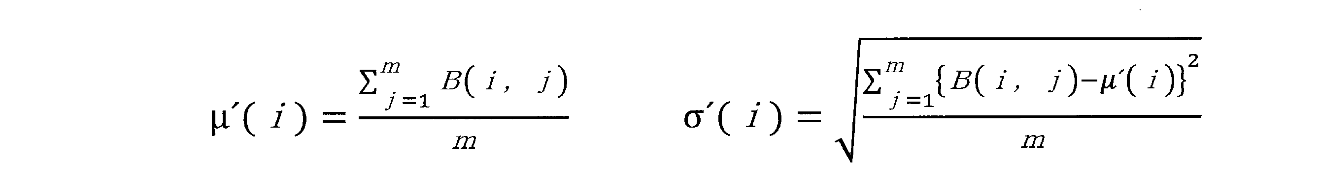
つまり、μ´(i)±{α×σ´(i)}の範囲外のデータは外れ値とみなし、無効データとして取り扱う。
That is, data outside the range of μ ′ (i) ± {α × σ ′ (i)} is regarded as an outlier and is treated as invalid data.
次に、制御処理装置54は、幅方向-輝度特性取得処理を実行する(ステップS33)。かかる工程が本実施形態における撮像領域輝度特性把握工程に相当し、これを実行する制御処理装置54の処理機能により、本実施形態における撮像領域輝度特性把握手段が構成されることとなる。
Next, the control processing device 54 executes a width direction-brightness characteristic acquisition process (step S33). This process corresponds to the imaging area luminance characteristic comprehension process in the present embodiment, and the imaging area luminance characteristic comprehension means in the present embodiment is configured by the processing function of the control processing device 54 that executes this process.
幅方向-輝度特性取得処理においては、まずステップS32の外れ値除去処理により、外れ値を無効データとした基準画像データA(図16参照)に対し、再度、分光スペクトルの波長分散方向(Y方向)と直交する各画素行(第1行目~第m行目)それぞれについて分布を求める。ここで、平均μ″(j)、標準偏差σ″(j)は、下記[数5]の関係式で表すことができる。
In the width direction-brightness characteristic acquisition process, first, outlier removal processing in step S32 causes the wavelength dispersion direction (Y direction) of the spectrum to be again determined with respect to the reference image data A (see FIG. 16) with outliers as invalid data. The distribution is determined for each of the pixel rows (first to m-th rows) orthogonal to. Here, the mean μ ′ ′ (j) and the standard deviation σ ′ ′ (j) can be expressed by the following equation [Equation 5].
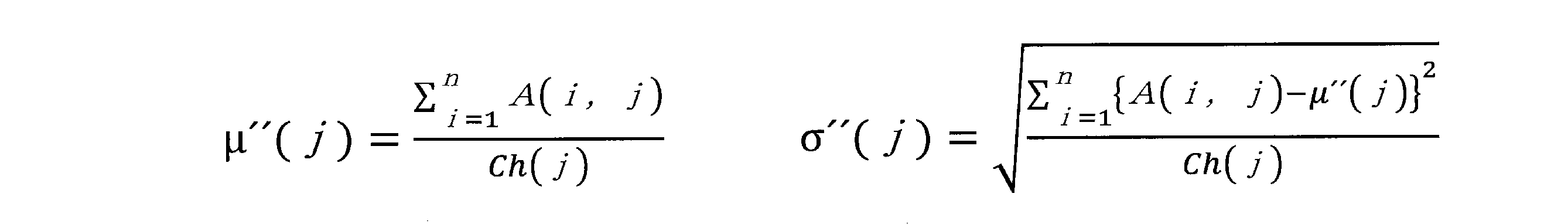
ここで、Ch(j)は、第j行目の画素行のデータ個数である。
Here, Ch (j) is the number of data in the j-th pixel row.
続いて、行方向に対し平均を0、分散を1に正規化する。これにより、例えば図18に示すように二次元展開される正規化データDが得られる。ここで、各座標位置(i,j)に係る正規化データ値D(i,j)は、下記[数6]の関係式で表すことができる。
Subsequently, the average is normalized to 0 and the variance is normalized to 1 in the row direction. As a result, for example, normalized data D which is two-dimensionally expanded as shown in FIG. 18 is obtained. Here, the normalized data value D (i, j) related to each coordinate position (i, j) can be expressed by the following relational expression [Expression 6].

続いて、正規化データDにおける、各画素列(第1列目~第n列目)それぞれについて、平均値Dave(i)を求める。平均値Dave(i)は、下記[数7]の関係式で表すことができる。
Subsequently, an average value D ave (i) is obtained for each pixel row (first to n-th columns) in the normalized data D. The average value D ave (i) can be expressed by the following equation (7).

ここで、Cv(i)は、第i列目の画素列のデータ個数である。
Here, Cv (i) is the number of data of the i-th pixel column.
そして、平均値Dave(i)に対して、最大値Rmax(i)を1、最小値Rmin(i)を0に正規化する。
Then, the maximum value R max (i) is normalized to 1 and the minimum value R min (i) is normalized to 0 with respect to the average value D ave (i).
これにより、行方向の最大~最小部分の割合T(i)が得られる。割合T(i)は、下記[数8]の関係式で表すことができる。
Thereby, the ratio T (i) of the maximum to the minimum in the row direction is obtained. The ratio T (i) can be expressed by the following equation [Equation 8].

次に、これを基準分光画像データAに当てはめ、絶対値データ(行方向全体)の割合を求める。
Next, this is applied to the reference spectral image data A to determine the ratio of absolute value data (entire row direction).
まず基準分光画像データAの各画素列(第1列目~第n列目)それぞれについて最大値Pmax(i)及び最小値Pmin(i)を求める。続いて、行方向における最大値Rmax(i)の位置における最大値Pmax(i)を求めると共に、行方向における最小値Rmin(i)の位置における最小値Pmin(i)を求める。これにより求められる行データの割合V(i)は、下記[数9]の関係式で表すことができる。
First, the maximum value P max (i) and the minimum value P min (i) are determined for each pixel row (first to n-th columns) of the reference spectral image data A. Subsequently, the maximum value P max (i) at the position of the maximum value R max (i) in the row direction is determined, and the minimum value P min (i) at the position of the minimum value R min (i) in the row direction is determined. The ratio V (i) of row data obtained by this can be expressed by the following equation [Equation 9].

上記一連の処理によって、幅方向-輝度特性取得処理(ステップS33)においては、幅方向-輝度特性として、行データの割合V(i)が取得されると共に、基準分光画像データAにおいて無効データを除いた全輝度値データの個数Cx、及び、基準分光画像データAにおいて無効データを除いた全輝度値データの合計値Sumxが取得されることとなる。
By the above series of processing, in the width direction-brightness characteristic acquisition processing (step S33), the ratio V (i) of the row data is obtained as the width direction-brightness characteristic, and invalid data in the reference spectral image data A is obtained. The number Cx of all luminance value data removed and the sum Sumx of all luminance value data excluding the invalid data in the reference spectral image data A is acquired.
基準分光画像データAにおいて無効データを除いた全輝度値データの個数Cx、及び、基準分光画像データAにおいて無効データを除いた全輝度値データの合計値Sumxは、下記[数10]の関係式で表すことができる。
The number Cx of all luminance value data excluding invalid data in the reference spectral image data A, and the total value Sumx of all luminance value data excluding invalid data in the reference spectral image data A are the relational expressions of the following [Equation 10] Can be represented by

次に、制御処理装置54は、波長-感度特性取得処理を実行する(ステップS34)。かかる工程が本実施形態における波長感度特性把握工程に相当し、これを実行する制御処理装置54の処理機能により、本実施形態における波長感度特性把握手段が構成されることとなる。
Next, the control processing unit 54 executes wavelength-sensitivity characteristic acquisition processing (step S34). This process corresponds to the wavelength sensitivity characteristic grasping process in the present embodiment, and the wavelength sensitivity characteristic grasping means in the present embodiment is constituted by the processing function of the control processing unit 54 which executes the process.
波長-感度特性取得処理においては、まずステップS32の外れ値除去処理により、外れ値を無効データとした基準画像データA(図16参照)に対し、分光スペクトルの波長分散方向(Y方向)と平行する各画素列(第1列目~第n列目)それぞれについて分布を求める。ここで、平均μ″(i)、標準偏差σ″(i)は、下記[数11]の関係式で表すことができる。
In the wavelength-sensitivity characteristic acquisition processing, first, outlier removal processing in step S32 is parallel to the wavelength dispersion direction (Y direction) of the spectral spectrum with respect to the reference image data A (see FIG. 16) with outliers as invalid data. The distribution is determined for each of the pixel columns (first to nth columns). Here, the average μ ′ ′ (i) and the standard deviation σ ′ ′ (i) can be expressed by the following equation [Equation 11].
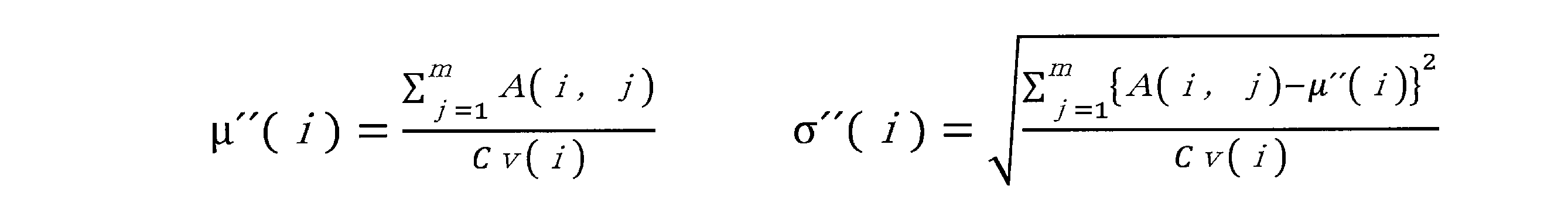
ここで、Cv(i)は、第i列目の画素列のデータ個数である。
Here, Cv (i) is the number of data of the i-th pixel column.
続いて、列方向に対し平均を0、分散を1に正規化する。これにより、例えば図18に示すように二次元展開される正規化データDが得られる。ここで、各座標位置(i,j)に係る正規化データ値D(i,j)は、下記[数12]の関係式で表すことができる。
Subsequently, the average is normalized to 0 and the variance is normalized to 1 in the column direction. As a result, for example, normalized data D which is two-dimensionally expanded as shown in FIG. 18 is obtained. Here, the normalized data value D (i, j) related to each coordinate position (i, j) can be expressed by the following equation [Equation 12].

続いて、正規化データDにおける、各画素行(第1行目~第m行目)それぞれについて、平均値Dave(j)を求める。平均値Dave(j)は、下記[数13]の関係式で表すことができる。
Subsequently, an average value D ave (j) is calculated for each pixel row (the first to m-th rows) in the normalized data D. The average value D ave (j) can be expressed by the following equation [Equation 13].

ここで、Ch(j)は、第j行目の画素行のデータ個数である。
Here, Ch (j) is the number of data in the j-th pixel row.
そして、平均値Dave(j)に対して、最大値Rmax(j)を1、最小値Rmin(j)を0に正規化する。
Then, the maximum value R max (j) is normalized to 1 and the minimum value R min (j) is normalized to 0 with respect to the average value D ave (j).
これにより、列方向の最大~最小部分の割合T(j)が得られる。割合T(j)は、下記[数14]の関係式で表すことができる。
Thereby, the ratio T (j) of the maximum to minimum in the column direction is obtained. The ratio T (j) can be expressed by the following equation [Equation 14].

次に、これを基準分光画像データAに当てはめ、絶対値データ(列方向全体)の割合を求める。
Next, this is applied to the reference spectral image data A to determine the ratio of absolute value data (entire column direction).
まず基準分光画像データAの各画素行(第1行目~第m行目)それぞれについて最大値Pmax(j)及び最小値Pmin(j)を求める。続いて、列方向における最大値Rmax(j)の位置における最大値Pmax(j)を求めると共に、列方向における最小値Rmin(j)の位置における最小値Pmin(j)を求める。これにより求められる列データの割合V(j)は、下記[数15]の関係式で表すことができる。
First, the maximum value P max (j) and the minimum value P min (j) are determined for each pixel row (first to m-th rows) of the reference spectral image data A. Subsequently, the maximum value P max (j) at the position of the maximum value R max (j) in the column direction is determined, and the minimum value P min (j) at the position of the minimum value R min (j) in the column direction is determined. The ratio V (j) of column data obtained by this can be expressed by the following equation [Equation 15].

上記一連の処理によって、波長-感度特性取得処理(ステップS34)においては、波長-感度特性として、列データの割合V(j)が取得されると共に、基準分光画像データAにおいて無効データを除いた全輝度値データの個数Cy、及び、基準分光画像データAにおいて無効データを除いた全輝度値データの合計値Sumyが取得されることとなる。
By the above series of processing, in the wavelength-sensitivity characteristic acquisition processing (step S34), the ratio V (j) of the column data is acquired as the wavelength-sensitivity characteristic, and the invalid data is removed from the reference spectral image data A The total number Sumy of all luminance value data excluding the invalid data in the reference spectral image data A is acquired.
基準分光画像データAにおいて無効データを除いた全輝度値データの個数Cy、及び、基準分光画像データAにおいて無効データを除いた全輝度値データの合計値Sumyは、下記[数16]の関係式で表すことができる。
The number Cy of all luminance value data excluding invalid data in the reference spectral image data A, and the total value Sumy of all luminance value data excluding invalid data in the reference spectral image data A are the relational expressions of the following [Equation 16] Can be represented by

次に、制御処理装置54は、補正値算出処理を実行する(ステップS35)。かかる工程が本実施形態における補正値算出工程に相当し、これを実行する制御処理装置54の処理機能により、本実施形態における補正値算出手段が構成されることとなる。
Next, the control processing device 54 executes a correction value calculation process (step S35). This process corresponds to the correction value calculation process in the present embodiment, and the correction value calculation means in the present embodiment is configured by the processing function of the control processing device 54 that executes this process.
補正値算出処理においては、まずステップS33において取得した行データの割合V(i)、及び、ステップS34において取得した列データの割合V(j)を掛け合わせ、二次元に展開する。
In the correction value calculation process, first, the ratio V (i) of row data acquired in step S33 and the ratio V (j) of column data acquired in step S34 are multiplied and expanded in two dimensions.
これにより、例えば図19に示すように全輝度値データの割合(分布)Eが得られる。つまり、各座標位置における「幅方向-輝度特性(輝度ムラ)を考慮した波長-感度特性」を取得することができる。ここで、座標(i,j)に係る割合E(i,j)は、下記[数17]の関係式で表すことができる。
Thereby, for example, as shown in FIG. 19, a ratio (distribution) E of all luminance value data is obtained. That is, it is possible to acquire “width direction—wavelength-sensitivity characteristics in consideration of luminance characteristics (uneven luminance)” at each coordinate position. Here, the ratio E (i, j) related to the coordinates (i, j) can be expressed by the following equation [Equation 17].

次に、全輝度値データの割合の平均Eaveを求める。平均Eaveは、下記[数18]の関係式で表すことができる。
Next, an average E ave of the ratio of all luminance value data is obtained. The average E ave can be expressed by the following equation [Equation 18].

次に、行データの割合V(i)、及び、列データの割合V(j)の算出に用いた基準分光画像データAの全輝度値データの平均値Faveを求める。平均値Faveは、下記[数19]の関係式で表すことができる。
Next, an average value F ave of all luminance value data of the reference spectral image data A used to calculate the ratio V (i) of row data and the ratio V (j) of column data is obtained. The average value F ave can be expressed by the following equation [Equation 19].

そして、全輝度値データの平均値Faveを割合の平均Eaveで割ることにより、補正値がMax値「1」となる場合の基準分光画像データAの輝度値データを求める。Max値は、下記[数20]の関係式で表すことができる。
Then, by dividing the average value F ave of all luminance value data by the average value E ave of the ratio, the luminance value data of the reference spectral image data A when the correction value becomes the Max value “1” is obtained. The Max value can be expressed by the following equation [Equation 20].

そして、これを図19に示す全輝度値データの割合Eに展開することにより、図20に示すような仮想的な補正後の画像データGを得ることができる。ここで、各座標(i,j)に係る補正後の輝度値データG(i,j)は、下記[数21]の関係式で表すことができる。
Then, the image data G after virtual correction as shown in FIG. 20 can be obtained by expanding this to the ratio E of all luminance value data shown in FIG. Here, the luminance value data G (i, j) after correction relating to each coordinate (i, j) can be expressed by the following equation [Equation 21].
各座標(i,j)に係る補正後の輝度値データG(i,j)を、各座標(i,j)に係る基準分光画像データAの輝度値データで割ることにより、図21に示すように、各座標位置(i,j)それぞれに係る補正値H(i,j)を得ることができる。ここで、各座標位置(i,j)に係る補正値H(i,j)は、下記[数22]の関係式で表すことができる。
The luminance value data G (i, j) after correction related to each coordinate (i, j) is divided by the luminance value data of the reference spectral image data A related to each coordinate (i, j), as shown in FIG. Thus, it is possible to obtain the correction value H (i, j) associated with each coordinate position (i, j). Here, the correction value H (i, j) related to each coordinate position (i, j) can be expressed by the following equation [Equation 22].

そして、補正値算出処理によって得られた各座標位置(i,j)に係る補正値H(i,j)を、記憶手段としての設定データ記憶装置76に記憶し、補正値設定ルーチンを終了する。
Then, the correction value H (i, j) relating to each coordinate position (i, j) obtained by the correction value calculation processing is stored in the setting data storage device 76 as storage means, and the correction value setting routine is ended. .
以上詳述したように、本実施形態によれば、上記第1実施形態と同様の作用効果が奏される。
As described above in detail, according to the present embodiment, the same effects as those of the first embodiment can be obtained.
特に本実施形態では、撮像素子65の波長感度特性、及び、撮像領域の輝度特性を把握するにあたり、正規化処理を行う構成となっているため、上記第1実施形態に比べ、検査精度のさらなる向上を図ることができる。
In particular, in the present embodiment, the wavelength sensitivity characteristic of the imaging device 65 and the luminance characteristic of the imaging region are configured to be subjected to normalization processing, so that inspection accuracy is further increased as compared with the first embodiment. It can improve.
加えて、本実施形態では、外れ値除去処理を行う構成となっているため、検査精度のさらなる向上を図ることができる。
In addition, in the present embodiment, the outlier removal process is performed, so that the inspection accuracy can be further improved.
尚、上記各実施形態の記載内容に限定されず、例えば次のように実施してもよい。勿論、以下において例示しない他の応用例、変更例も当然可能である。
In addition, it is not limited to the description content of said each embodiment, For example, you may implement as follows. Of course, other applications and modifications not illustrated below are naturally possible.
(a)上記各実施形態では、内容物(検査対象物)が錠剤5である場合について具体化しているが、内容物の種別、形状等については特に限定されるものではなく、例えばカプセル剤やサプリメント、食品等であってもよい。また、錠剤には素錠や糖衣錠などの固形製剤が含まれる。
(A) In each of the above embodiments, the case where the content (the test object) is the tablet 5 is embodied, but the type, shape, and the like of the content are not particularly limited. It may be a supplement, food or the like. Tablets also include solid preparations such as uncoated tablets and sugar-coated tablets.
(b)容器フィルム3やカバーフィルム4の材料は、上記各実施形態に限定されるものではなく、他の材質のものを採用してもよい。例えば容器フィルム3が、アルミラミネートフィルムなど、アルミニウムを主材料とした金属材料により形成された構成としてもよい。
(B) The materials of the container film 3 and the cover film 4 are not limited to the above-described embodiments, and other materials may be adopted. For example, the container film 3 may be formed of a metal material whose main material is aluminum, such as an aluminum laminated film.
(c)PTPシート1におけるポケット部2の配列や個数に関しては、上記各実施形態に何ら限定されるものではなく、例えば3列12個のポケット部を有するタイプをはじめ、様々な配列、個数からなるPTPシートを採用することができる。
(C) The arrangement and the number of the pocket portions 2 in the PTP sheet 1 are not limited to the above embodiments. For example, various arrangements and numbers are available, including a type having 12 pockets in three rows. Can be adopted.
(d)上記各実施形態では、ポケット部2に錠剤5が充填された後工程かつ容器フィルム3に対しカバーフィルム4が取着される前工程において、検査装置22による異品種混入検査が行われる構成となっている。
(D) In each of the above-described embodiments, in the subsequent step in which the tablet 5 is filled in the pocket portion 2 and the previous step in which the cover film 4 is attached to the container film 3, different types of contamination testing is performed by the inspection device 22. It is a structure.
これに限らず、例えば容器フィルム3に対しカバーフィルム4が取着された後工程かつPTPフィルム6からPTPシート1が打抜かれる前工程において、PTPフィルム6の容器フィルム3側から検査装置22による異品種混入検査が行われる構成としてもよい。
The invention is not limited to this, and for example, in the post-process where the cover film 4 is attached to the container film 3 and the pre-process where the PTP sheet 1 is punched from the PTP film 6 The configuration may be such that different-mixture inspection is performed.
また、PTPフィルム6からPTPシート1が打抜かれた後工程において、取出しコンベア39によって搬送されているPTPシート1の容器フィルム3側から検査装置22による異品種混入検査が行われる構成としてもよい。
Further, in a process after punching the PTP sheet 1 from the PTP film 6, the different type mixture inspection by the inspection device 22 may be performed from the side of the container film 3 of the PTP sheet 1 conveyed by the pickup conveyor 39.
この際、検査装置22がPTP包装機10内に設けられた構成(インライン)に代えて、PTP包装機10とは別に、オフラインでPTPシート1を検査する装置として検査装置22を備えた構成としてもよい。また、かかる場合に、PTPシート1を搬送可能な搬送手段を検査装置22に備えた構成としてもよい。
At this time, the inspection apparatus 22 is provided with the inspection apparatus 22 as an apparatus for inspecting the PTP sheet 1 off-line separately from the PTP packing machine 10 instead of the configuration (inline) provided in the PTP packing machine 10 It is also good. Further, in such a case, the inspection device 22 may be provided with a transport unit capable of transporting the PTP sheet 1.
また、ポケット部2に錠剤5が充填される前工程において、検査装置22による異品種混入検査が行われる構成としてもよい。例えば錠剤充填装置21に錠剤5を投入する前段階に検査を行う構成としてもよい。つまり、PTP包装機10とは別に、オフラインで錠剤5を検査する装置として検査装置22を備えた構成としてもよい。
In addition, in the pre-process in which the tablet 5 is filled in the pocket portion 2, the different-type mixture inspection by the inspection device 22 may be performed. For example, the inspection may be performed before the tablet 5 is put into the tablet filling device 21. That is, apart from the PTP packaging machine 10, the inspection apparatus 22 may be provided as an apparatus for inspecting the tablets 5 off-line.
(e)照明装置52及び撮像装置53の構成は上記各実施形態に限定されるものではない。例えば二次元分光器62に代えて、分光手段として反射型回折格子やプリズム等を採用した構成としてもよい。
(E) The configurations of the illumination device 52 and the imaging device 53 are not limited to the above embodiments. For example, instead of the two-dimensional spectroscope 62, a configuration may be adopted in which a reflection type diffraction grating, a prism, or the like is adopted as the spectroscopic means.
(f)上記各実施形態では、スペクトルデータを主成分分析(PCA)により分析する構成となっているが、これに限らず、PLS回帰分析など、他の公知の方法を用いて分析する構成としてもよい。
(F) In the above embodiments, spectral data is analyzed by principal component analysis (PCA). However, the present invention is not limited to this, and other known methods such as PLS regression analysis may be used to analyze It is also good.
(g)上記各実施形態に係る補正値設定ルーチンにおいては、撮像素子65の波長感度特性、及び、撮像領域の輝度特性を把握し、これらを基に補正値を算出する構成となっている。これに限らず、少なくとも撮像素子65の波長感度特性を把握し、これを基に補正値を算出する構成としてもよい。
(G) In the correction value setting routine according to each of the above embodiments, the wavelength sensitivity characteristic of the imaging device 65 and the luminance characteristic of the imaging area are grasped, and the correction value is calculated based on these. Not limited to this, at least the wavelength sensitivity characteristic of the imaging device 65 may be grasped, and the correction value may be calculated based on this.
(h)波長-感度特性取得処理の内容、及び/又は、幅方向-輝度特性取得処理の内容は、上記各実施形態に係る内容に限定されるものではなく、他の構成を採用してもよい。
(H) The content of the wavelength-sensitivity characteristic acquisition processing and / or the content of the width direction-luminance characteristic acquisition processing is not limited to the content according to each of the above embodiments, and other configurations may be adopted. Good.
例えば上記第1実施形態では、所定の画素行又は画素列に属する画素の輝度値を平均する平均処理を行い、これにより算出された平均輝度値を該画素行又は該画素列に係る特性とする構成となっているが、これに代えて、例えば所定の画素行又は画素列に属する画素の輝度値を加算する加算処理を行い、これにより算出された加算輝度値を該画素行又は該画素列に係る特性とする構成としてもよい。
For example, in the first embodiment, the averaging process of averaging the luminance values of the pixels belonging to a predetermined pixel row or pixel column is performed, and the average luminance value calculated thereby is used as the characteristic of the pixel row or the pixel column. Although it has a configuration, instead of this, for example, an addition process of adding the luminance values of pixels belonging to a predetermined pixel row or pixel column is performed, and the addition luminance value calculated by this is used as the pixel row or the pixel column It is good also as composition which makes it the characteristic concerning.
(i)上記第2実施形態では、正規化処理を行うにあたり、例えば平均を第1値としての「0」、分散を第2値としての「1」に正規化しているが、第1値及び/又は第2値は「0」や「1」に限定されるものではなく、他の値としてもよい。
(I) In the second embodiment, when performing the normalization process, for example, the average is normalized to “0” as the first value, and the variance is normalized to “1” as the second value. The second value is not limited to “0” or “1”, and may be another value.
(j)上記第1実施形態において、外れ値除去処理を行う構成としてもよいし、上記第2実施形態において、外れ値除去処理を省略した構成としてもよい。
(J) In the first embodiment, the outlier removal process may be performed. In the second embodiment, the outlier removal process may be omitted.
1…PTPシート、2…ポケット部、3…容器フィルム、4…カバーフィルム、5…錠剤、10…PTP包装機、22…検査装置、52…照明装置、53…撮像装置、54…制御処理装置、62…二次元分光器、62a…スリット、63…カメラ、64…受光素子、65…撮像素子、74…画像データ記憶装置、76…設定データ記憶装置、LS…分光スペクトル。
DESCRIPTION OF SYMBOLS 1 ... PTP sheet, 2 ... Pocket part, 3 ... Container film, 4 ... Cover film, 5 ... Tablet, 10 ... PTP packing machine, 22 ... Inspection apparatus, 52 ... Lighting apparatus, 53 ... Imaging apparatus, 54 ... Control processing apparatus , 62: two-dimensional spectroscope, 62a: slit, 63: camera, 64: light receiving element, 65: imaging element, 74: image data storage device, 76: setting data storage device, L S : spectral spectrum.
Claims (5)
- 対象物に対し近赤外光を照射可能な照射手段と、
前記近赤外光が照射された前記対象物から反射される反射光を分光可能な分光手段と、
複数の受光素子が行列状に配置された撮像素子を有し、前記分光手段にて分光された前記反射光に係る分光スペクトルを撮像可能な撮像手段とを備え、
前記撮像手段により取得された分光画像データを基に、分光分析を利用して所定の検査を行う検査装置であって、
前記撮像手段により所定の基準対象物に係る分光スペクトルを撮像し取得した基準分光画像データにおける、前記分光スペクトルの波長分散方向と直交する各画素行及び/又は前記波長分散方向と平行する各画素列それぞれについて、該画素行又は該画素列に属する画素の輝度値を用いて所定の演算処理を実行し、各画素行毎の特性を求めることにより、前記照射手段から照射される近赤外光の下での前記撮像素子の波長感度特性を把握する波長感度特性把握手段と、
前記基準分光画像データの各画素の輝度値、及び、該画素が属する画素行に係る前記特性を基に、前記基準分光画像データの各画素に対応する座標位置それぞれに係る補正値を算出する補正値算出手段と、
前記撮像手段により所定の検査対象物を撮像し取得した検査分光画像データの各画素の輝度値を、該画素に対応する座標位置に係る前記補正値を基に補正する画像補正手段と、
前記検査分光画像データを補正した補正分光画像データを基にスペクトルデータを取得可能なスペクトルデータ取得手段と、
前記スペクトルデータを基に、前記検査対象物について所定の分析処理を行う分析手段とを備えたことを特徴とする検査装置。 An irradiation unit capable of irradiating near infrared light to the object;
Spectroscopic means capable of dispersing the reflected light reflected from the object irradiated with the near infrared light;
The imaging device includes: an imaging device in which a plurality of light receiving devices are arranged in a matrix; and an imaging device capable of imaging a spectrum relating to the reflected light dispersed by the dispersing device;
An inspection apparatus that performs a predetermined inspection using spectral analysis based on spectral image data acquired by the imaging unit.
Each pixel row orthogonal to the wavelength dispersion direction of the spectral spectrum and / or each pixel row parallel to the wavelength dispersion direction in reference spectral image data obtained by imaging the spectral spectrum of a predetermined reference object by the imaging means and acquired For each, by performing predetermined arithmetic processing using the luminance value of the pixel row or the pixels belonging to the pixel column to obtain the characteristics for each pixel row, the near infrared light emitted from the irradiation unit Wavelength sensitivity characteristic grasping means for grasping the wavelength sensitivity characteristic of the image pickup device under;
Based on the luminance value of each pixel of the reference spectral image data and the characteristics of the pixel row to which the pixel belongs, a correction value is calculated for each coordinate position corresponding to each pixel of the reference spectral image data Value calculation means,
An image correction unit that corrects a luminance value of each pixel of inspection spectral image data acquired by imaging a predetermined inspection object by the imaging unit based on the correction value related to a coordinate position corresponding to the pixel;
Spectrum data acquisition means capable of acquiring spectrum data based on the corrected spectral image data obtained by correcting the inspection spectral image data;
An inspection apparatus comprising: analysis means for performing a predetermined analysis process on the inspection object based on the spectrum data. - 対象物に対し近赤外光を照射可能な照射手段と、
前記近赤外光が照射された前記対象物から反射される反射光を分光可能な分光手段と、
複数の受光素子が行列状に配置された撮像素子を有し、前記分光手段にて分光された前記反射光に係る分光スペクトルを撮像可能な撮像手段とを備え、
前記撮像手段により取得された分光画像データを基に、分光分析を利用して所定の検査を行う検査装置であって、
前記撮像手段により所定の基準対象物に係る分光スペクトルを撮像し取得した基準分光画像データにおける、前記分光スペクトルの波長分散方向と直交する各画素行及び/又は前記波長分散方向と平行する各画素列それぞれについて、該画素行又は該画素列に属する画素の輝度値を用いて所定の演算処理を実行し、各画素行毎の特性を求めることにより、前記照射手段から照射される近赤外光の下での前記撮像素子の波長感度特性を把握する波長感度特性把握手段と、
前記基準分光画像データにおける、前記波長分散方向と平行する各画素列及び/又は前記波長分散方向と直交する各画素行それぞれについて、該画素列又は該画素行に属する画素の輝度値を用いて所定の演算処理を実行し、各画素列毎の特性を求めることにより、前記照射手段から照射される近赤外光の下での撮像領域の輝度特性を把握する撮像領域輝度特性把握手段と、
前記基準分光画像データの各画素の輝度値、並びに、該画素が属する画素行に係る前記特性、及び、該画素が属する画素列に係る前記特性を基に、前記基準分光画像データの各画素に対応する座標位置それぞれに係る補正値を算出する補正値算出手段と、
前記撮像手段により所定の検査対象物を撮像し取得した検査分光画像データの各画素の輝度値を、該画素に対応する座標位置に係る前記補正値を基に補正する画像補正手段と、
前記検査分光画像データを補正した補正分光画像データを基にスペクトルデータを取得可能なスペクトルデータ取得手段と、
前記スペクトルデータを基に、前記検査対象物について所定の分析処理を行う分析手段とを備えたことを特徴とする検査装置。 An irradiation unit capable of irradiating near infrared light to the object;
Spectroscopic means capable of dispersing the reflected light reflected from the object irradiated with the near infrared light;
The imaging device includes: an imaging device in which a plurality of light receiving devices are arranged in a matrix; and an imaging device capable of imaging a spectrum relating to the reflected light dispersed by the dispersing device;
An inspection apparatus that performs a predetermined inspection using spectral analysis based on spectral image data acquired by the imaging unit.
Each pixel row orthogonal to the wavelength dispersion direction of the spectral spectrum and / or each pixel row parallel to the wavelength dispersion direction in reference spectral image data obtained by imaging the spectral spectrum of a predetermined reference object by the imaging means and acquired For each, by performing predetermined arithmetic processing using the luminance value of the pixel row or the pixels belonging to the pixel column to obtain the characteristics for each pixel row, the near infrared light emitted from the irradiation unit Wavelength sensitivity characteristic grasping means for grasping the wavelength sensitivity characteristic of the image pickup device under;
For each pixel column parallel to the wavelength dispersion direction and / or each pixel row orthogonal to the wavelength dispersion direction in the reference spectral image data, predetermined using the luminance value of the pixel belonging to the pixel column or the pixel row An imaging area luminance characteristic grasping means for grasping the luminance characteristic of the imaging area under the near infrared light irradiated from the irradiation means by executing the arithmetic processing of
On each pixel of the reference spectral image data, based on the luminance value of each pixel of the reference spectral image data, the characteristic of the pixel row to which the pixel belongs, and the characteristic of the pixel column to which the pixel belongs Correction value calculation means for calculating a correction value associated with each corresponding coordinate position;
An image correction unit that corrects a luminance value of each pixel of inspection spectral image data acquired by imaging a predetermined inspection object by the imaging unit based on the correction value related to a coordinate position corresponding to the pixel;
Spectrum data acquisition means capable of acquiring spectrum data based on the corrected spectral image data obtained by correcting the inspection spectral image data;
An inspection apparatus comprising: analysis means for performing a predetermined analysis process on the inspection object based on the spectrum data. - 容器フィルムに形成されたポケット部に所定の内容物が収容され、該ポケット部を塞ぐようにカバーフィルムが取着されてなるPTPシートを製造するためのPTP包装機であって、
帯状に搬送される前記容器フィルムに対し前記ポケット部を形成するポケット部形成手段と、
前記ポケット部に前記内容物を充填する充填手段と、
前記ポケット部に前記内容物が充填された前記容器フィルムに対し、前記ポケット部を塞ぐようにして帯状の前記カバーフィルムを取着する取着手段と、
前記容器フィルムに前記カバーフィルムが取着された帯状体から前記PTPシートを切離す切離手段と、
前記内容物を前記検査対象物として検査を行う請求項1又は2に記載の検査装置とを備えたことを特徴とするPTP包装機。 A PTP packaging machine for producing a PTP sheet in which a predetermined content is accommodated in a pocket portion formed in a container film, and a cover film is attached so as to close the pocket portion,
Pocket portion forming means for forming the pocket portion with respect to the container film conveyed in a belt shape;
Filling means for filling the contents in the pocket portion;
An attachment means for attaching the strip-like cover film so as to close the pocket portion to the container film in which the content is filled in the pocket portion;
Separating means for separating the PTP sheet from a strip in which the cover film is attached to the container film;
A PTP packaging machine comprising: the inspection device according to claim 1 or 2 which inspects the contents as the inspection object. - 対象物に対し近赤外光を照射可能な照射手段と、
前記近赤外光が照射された前記対象物から反射される反射光を分光可能な分光手段と、
複数の受光素子が行列状に配置された撮像素子を有し、前記分光手段にて分光された前記反射光に係る分光スペクトルを撮像可能な撮像手段とを備え、
前記撮像手段により取得された分光画像データを基に、分光分析を利用して所定の検査を行う検査装置の較正方法であって、
前記撮像手段により所定の基準対象物に係る分光スペクトルを撮像し取得した基準分光画像データにおける、前記分光スペクトルの波長分散方向と直交する各画素行及び/又は前記波長分散方向と平行する各画素列それぞれについて、該画素行又は該画素列に属する画素の輝度値を用いて所定の演算処理を実行し、各画素行毎の特性を求めることにより、前記照射手段から照射される近赤外光の下での前記撮像素子の波長感度特性を把握する波長感度特性把握工程と、
前記基準分光画像データの各画素の輝度値、及び、該画素が属する画素行に係る前記特性を基に、前記基準分光画像データの各画素に対応する座標位置それぞれに係る補正値を算出する補正値算出工程と、
前記撮像手段により所定の検査対象物を撮像し取得した検査分光画像データの各画素の輝度値を、該画素に対応する座標位置に係る前記補正値を基に補正する画像補正工程とを備えたことを特徴とする検査装置の較正方法。 An irradiation unit capable of irradiating near infrared light to the object;
Spectroscopic means capable of dispersing the reflected light reflected from the object irradiated with the near infrared light;
The imaging device includes: an imaging device in which a plurality of light receiving devices are arranged in a matrix; and an imaging device capable of imaging a spectrum relating to the reflected light dispersed by the dispersing device;
A calibration method of an inspection apparatus for performing a predetermined inspection using spectral analysis based on spectral image data acquired by the imaging unit,
Each pixel row orthogonal to the wavelength dispersion direction of the spectral spectrum and / or each pixel row parallel to the wavelength dispersion direction in reference spectral image data obtained by imaging the spectral spectrum of a predetermined reference object by the imaging means and acquired For each, by performing predetermined arithmetic processing using the luminance value of the pixel row or the pixels belonging to the pixel column to obtain the characteristics for each pixel row, the near infrared light emitted from the irradiation unit Wavelength sensitivity characteristic grasping step of grasping wavelength sensitivity characteristic of the image pickup device under the following conditions;
Based on the luminance value of each pixel of the reference spectral image data and the characteristics of the pixel row to which the pixel belongs, a correction value is calculated for each coordinate position corresponding to each pixel of the reference spectral image data Value calculation process,
And correcting the luminance value of each pixel of the inspection spectral image data acquired by imaging the predetermined inspection object by the imaging means based on the correction value at the coordinate position corresponding to the pixel. A calibration method of an inspection apparatus characterized in that. - 対象物に対し近赤外光を照射可能な照射手段と、
前記近赤外光が照射された前記対象物から反射される反射光を分光可能な分光手段と、
複数の受光素子が行列状に配置された撮像素子を有し、前記分光手段にて分光された前記反射光に係る分光スペクトルを撮像可能な撮像手段とを備え、
前記撮像手段により取得された分光画像データを基に、分光分析を利用して所定の検査を行う検査装置の較正方法であって、
前記撮像手段により所定の基準対象物に係る分光スペクトルを撮像し取得した基準分光画像データにおける、前記分光スペクトルの波長分散方向と直交する各画素行及び/又は前記波長分散方向と平行する各画素列それぞれについて、該画素行又は該画素列に属する画素の輝度値を用いて所定の演算処理を実行し、各画素行毎の特性を求めることにより、前記照射手段から照射される近赤外光の下での前記撮像素子の波長感度特性を把握する波長感度特性把握工程と、
前記基準分光画像データにおける、前記波長分散方向と平行する各画素列及び/又は前記波長分散方向と直交する各画素行それぞれについて、該画素列又は該画素行に属する画素の輝度値を用いて所定の演算処理を実行し、各画素列毎の特性を求めることにより、前記照射手段から照射される近赤外光の下での撮像領域の輝度特性を把握する撮像領域輝度特性把握工程と、
前記基準分光画像データの各画素の輝度値、並びに、該画素が属する画素行に係る前記特性、及び、該画素が属する画素列に係る前記特性を基に、前記基準分光画像データの各画素に対応する座標位置それぞれに係る補正値を算出する補正値算出工程と、
前記撮像手段により所定の検査対象物を撮像し取得した検査分光画像データの各画素の輝度値を、該画素に対応する座標位置に係る前記補正値を基に補正する画像補正工程とを備えたことを特徴とする検査装置の較正方法。 An irradiation unit capable of irradiating near infrared light to the object;
Spectroscopic means capable of dispersing the reflected light reflected from the object irradiated with the near infrared light;
The imaging device includes: an imaging device in which a plurality of light receiving devices are arranged in a matrix; and an imaging device capable of imaging a spectrum relating to the reflected light dispersed by the dispersing device;
A calibration method of an inspection apparatus for performing a predetermined inspection using spectral analysis based on spectral image data acquired by the imaging unit,
Each pixel row orthogonal to the wavelength dispersion direction of the spectral spectrum and / or each pixel row parallel to the wavelength dispersion direction in reference spectral image data obtained by imaging the spectral spectrum of a predetermined reference object by the imaging means and acquired For each, by performing predetermined arithmetic processing using the luminance value of the pixel row or the pixels belonging to the pixel column to obtain the characteristics for each pixel row, the near infrared light emitted from the irradiation unit Wavelength sensitivity characteristic grasping step of grasping wavelength sensitivity characteristic of the image pickup device under the following conditions;
For each pixel column parallel to the wavelength dispersion direction and / or each pixel row orthogonal to the wavelength dispersion direction in the reference spectral image data, predetermined using the luminance value of the pixel belonging to the pixel column or the pixel row An imaging area luminance characteristic grasping step of grasping the luminance characteristic of the imaging area under the near infrared light irradiated from the irradiation unit by executing the arithmetic processing of and determining the characteristic of each pixel row;
On each pixel of the reference spectral image data, based on the luminance value of each pixel of the reference spectral image data, the characteristic of the pixel row to which the pixel belongs, and the characteristic of the pixel column to which the pixel belongs A correction value calculation step of calculating a correction value related to each of the corresponding coordinate positions;
And correcting the luminance value of each pixel of the inspection spectral image data acquired by imaging the predetermined inspection object by the imaging means based on the correction value at the coordinate position corresponding to the pixel. A calibration method of an inspection apparatus characterized in that.
Priority Applications (3)
| Application Number | Priority Date | Filing Date | Title |
|---|---|---|---|
| CN201880087558.4A CN111630369B (en) | 2018-01-24 | 2018-09-07 | Inspection device, PTP packaging machine, and correction method for inspection device |
| EP18902271.8A EP3745113A4 (en) | 2018-01-24 | 2018-09-07 | Inspection device, ptp packaging machine, and calibration method of inspection device |
| US16/919,490 US20200333256A1 (en) | 2018-01-24 | 2020-07-02 | Inspection device, ptp packaging machine and calibration method of inspection device |
Applications Claiming Priority (2)
| Application Number | Priority Date | Filing Date | Title |
|---|---|---|---|
| JP2018009794A JP6568245B2 (en) | 2018-01-24 | 2018-01-24 | Inspection device, PTP packaging machine, and calibration method for inspection device |
| JP2018-009794 | 2018-01-24 |
Related Child Applications (1)
| Application Number | Title | Priority Date | Filing Date |
|---|---|---|---|
| US16/919,490 Continuation US20200333256A1 (en) | 2018-01-24 | 2020-07-02 | Inspection device, ptp packaging machine and calibration method of inspection device |
Publications (1)
| Publication Number | Publication Date |
|---|---|
| WO2019146152A1 true WO2019146152A1 (en) | 2019-08-01 |
Family
ID=67395929
Family Applications (1)
| Application Number | Title | Priority Date | Filing Date |
|---|---|---|---|
| PCT/JP2018/033210 WO2019146152A1 (en) | 2018-01-24 | 2018-09-07 | Inspection device, ptp packaging machine, and calibration method of inspection device |
Country Status (5)
| Country | Link |
|---|---|
| US (1) | US20200333256A1 (en) |
| EP (1) | EP3745113A4 (en) |
| JP (1) | JP6568245B2 (en) |
| CN (1) | CN111630369B (en) |
| WO (1) | WO2019146152A1 (en) |
Families Citing this family (4)
| Publication number | Priority date | Publication date | Assignee | Title |
|---|---|---|---|---|
| JP6763059B1 (en) * | 2019-05-16 | 2020-09-30 | Ckd株式会社 | Inspection equipment, packaging machine and packaging inspection method |
| NL2027213B1 (en) * | 2020-12-03 | 2022-07-06 | Ziuz Holding B V | Inspecting medicine objects based on hyperspectral imaging |
| WO2022117874A1 (en) * | 2020-12-03 | 2022-06-09 | Ziuz Holding B.V. | Inspecting medicine objects based on hyperspectral imaging |
| JP7429205B2 (en) | 2021-05-13 | 2024-02-07 | アンリツ株式会社 | Article inspection equipment |
Citations (15)
| Publication number | Priority date | Publication date | Assignee | Title |
|---|---|---|---|---|
| JPH02226027A (en) * | 1989-02-27 | 1990-09-07 | Hamamatsu Photonics Kk | Spectroscopic analyser |
| JPH0432729A (en) | 1990-05-30 | 1992-02-04 | Denki Kagaku Keiki Kk | Fourier transformation type spectral analyzing device |
| JP2003107008A (en) * | 2001-09-28 | 2003-04-09 | Web Tec Kk | Method for detecting density and surface state of printing sheet |
| WO2005038443A1 (en) * | 2003-10-17 | 2005-04-28 | Astellas Pharma, Inc. | Different-kind-of-object detector employing plane spectrometer |
| WO2005040741A1 (en) * | 2003-10-29 | 2005-05-06 | Saika Technological Institute Foundation | Spectrophotometer |
| JP2006170669A (en) * | 2004-12-13 | 2006-06-29 | Mitsui Mining & Smelting Co Ltd | Quality inspection device of vegetables and fruits |
| JP2010112887A (en) * | 2008-11-07 | 2010-05-20 | Astellas Pharma Inc | Principal component analysis method, principal component analyzer, different kind article detection device, principal component analysis program, and recording medium for recording the principal component analysis program |
| JP2010175528A (en) * | 2009-02-02 | 2010-08-12 | Mutual Corp | Inspection apparatus |
| WO2011055405A1 (en) * | 2009-11-04 | 2011-05-12 | 株式会社ニレコ | Spectral information read device |
| WO2013002291A1 (en) | 2011-06-28 | 2013-01-03 | 大塚製薬株式会社 | Drug inspection device and drug inspection method |
| WO2015136620A1 (en) * | 2014-03-11 | 2015-09-17 | 株式会社東芝 | Tablet inspection device, tablet inspection method, and tablet inspection program |
| JP2015203586A (en) * | 2014-04-11 | 2015-11-16 | 住友電気工業株式会社 | inspection method |
| JP2016043970A (en) * | 2014-08-25 | 2016-04-04 | Ckd株式会社 | PTP packaging machine |
| JP2016164083A (en) * | 2015-02-26 | 2016-09-08 | Ckd株式会社 | Manufacturing device for ptp sheet and manufacturing method for ptp sheet |
| JP6235684B1 (en) * | 2016-11-29 | 2017-11-22 | Ckd株式会社 | Inspection device and PTP packaging machine |
Family Cites Families (15)
| Publication number | Priority date | Publication date | Assignee | Title |
|---|---|---|---|---|
| JPS58103604A (en) * | 1981-12-16 | 1983-06-20 | Teijin Ltd | Method and device for measuring thickness of film |
| US5131755A (en) * | 1988-02-19 | 1992-07-21 | Chadwick Curt H | Automatic high speed optical inspection system |
| SE512098C2 (en) * | 1998-05-19 | 2000-01-24 | Agrovision Ab | Concentration determination of one component in a mixture of at least two components |
| US7459696B2 (en) * | 2003-04-18 | 2008-12-02 | Schomacker Kevin T | Methods and apparatus for calibrating spectral data |
| JP2006262274A (en) * | 2005-03-18 | 2006-09-28 | Seiko Epson Corp | Imaging data correcting method, imaging data correcting device, imaging object inspecting method, imaging object inspecting device, imaging data correcting program, and storage medium |
| US8144320B2 (en) * | 2006-11-22 | 2012-03-27 | Optopo, Inc. | Method and apparatus for reconstructing optical spectra in a static multimode multiplex spectrometer |
| JP2009224971A (en) * | 2008-03-14 | 2009-10-01 | Omron Corp | Image processing device |
| JP2012088199A (en) * | 2010-10-20 | 2012-05-10 | Yamaha Motor Co Ltd | Method and apparatus for inspecting foreign matter |
| JP5526183B2 (en) * | 2012-04-25 | 2014-06-18 | Ckd株式会社 | Inspection device and PTP packaging machine |
| JP5697168B2 (en) * | 2012-08-07 | 2015-04-08 | Ckd株式会社 | Inspection device and PTP packaging machine |
| US9546904B2 (en) * | 2013-03-15 | 2017-01-17 | P & P Optica Inc. | Apparatus and method for optimizing data capture and data correction for spectroscopic analysis |
| JP2014215177A (en) * | 2013-04-25 | 2014-11-17 | 住友電気工業株式会社 | Inspection device and inspection method |
| JP6068375B2 (en) * | 2014-03-03 | 2017-01-25 | エバ・ジャパン 株式会社 | Spectral radiance meter |
| WO2017179243A1 (en) * | 2016-04-12 | 2017-10-19 | 新日鐵住金株式会社 | Device for capturing image of object to be inspected, method for capturing image of object to be inspected, surface inspecting device and surface inspecting method |
| JP6706301B2 (en) * | 2018-09-28 | 2020-06-03 | Ckd株式会社 | Inspection device, PTP packaging machine, and PTP sheet manufacturing method |
-
2018
- 2018-01-24 JP JP2018009794A patent/JP6568245B2/en active Active
- 2018-09-07 CN CN201880087558.4A patent/CN111630369B/en active Active
- 2018-09-07 WO PCT/JP2018/033210 patent/WO2019146152A1/en unknown
- 2018-09-07 EP EP18902271.8A patent/EP3745113A4/en active Pending
-
2020
- 2020-07-02 US US16/919,490 patent/US20200333256A1/en active Pending
Patent Citations (15)
| Publication number | Priority date | Publication date | Assignee | Title |
|---|---|---|---|---|
| JPH02226027A (en) * | 1989-02-27 | 1990-09-07 | Hamamatsu Photonics Kk | Spectroscopic analyser |
| JPH0432729A (en) | 1990-05-30 | 1992-02-04 | Denki Kagaku Keiki Kk | Fourier transformation type spectral analyzing device |
| JP2003107008A (en) * | 2001-09-28 | 2003-04-09 | Web Tec Kk | Method for detecting density and surface state of printing sheet |
| WO2005038443A1 (en) * | 2003-10-17 | 2005-04-28 | Astellas Pharma, Inc. | Different-kind-of-object detector employing plane spectrometer |
| WO2005040741A1 (en) * | 2003-10-29 | 2005-05-06 | Saika Technological Institute Foundation | Spectrophotometer |
| JP2006170669A (en) * | 2004-12-13 | 2006-06-29 | Mitsui Mining & Smelting Co Ltd | Quality inspection device of vegetables and fruits |
| JP2010112887A (en) * | 2008-11-07 | 2010-05-20 | Astellas Pharma Inc | Principal component analysis method, principal component analyzer, different kind article detection device, principal component analysis program, and recording medium for recording the principal component analysis program |
| JP2010175528A (en) * | 2009-02-02 | 2010-08-12 | Mutual Corp | Inspection apparatus |
| WO2011055405A1 (en) * | 2009-11-04 | 2011-05-12 | 株式会社ニレコ | Spectral information read device |
| WO2013002291A1 (en) | 2011-06-28 | 2013-01-03 | 大塚製薬株式会社 | Drug inspection device and drug inspection method |
| WO2015136620A1 (en) * | 2014-03-11 | 2015-09-17 | 株式会社東芝 | Tablet inspection device, tablet inspection method, and tablet inspection program |
| JP2015203586A (en) * | 2014-04-11 | 2015-11-16 | 住友電気工業株式会社 | inspection method |
| JP2016043970A (en) * | 2014-08-25 | 2016-04-04 | Ckd株式会社 | PTP packaging machine |
| JP2016164083A (en) * | 2015-02-26 | 2016-09-08 | Ckd株式会社 | Manufacturing device for ptp sheet and manufacturing method for ptp sheet |
| JP6235684B1 (en) * | 2016-11-29 | 2017-11-22 | Ckd株式会社 | Inspection device and PTP packaging machine |
Non-Patent Citations (1)
| Title |
|---|
| See also references of EP3745113A4 |
Also Published As
| Publication number | Publication date |
|---|---|
| EP3745113A4 (en) | 2021-10-20 |
| EP3745113A1 (en) | 2020-12-02 |
| US20200333256A1 (en) | 2020-10-22 |
| JP6568245B2 (en) | 2019-08-28 |
| CN111630369B (en) | 2023-05-30 |
| CN111630369A (en) | 2020-09-04 |
| JP2019128250A (en) | 2019-08-01 |
Similar Documents
| Publication | Publication Date | Title |
|---|---|---|
| WO2019146152A1 (en) | Inspection device, ptp packaging machine, and calibration method of inspection device | |
| JP6329668B1 (en) | Inspection apparatus, PTP packaging machine, and PTP sheet manufacturing method | |
| JP6786565B2 (en) | Inspection equipment, PTP packaging machine and PTP sheet manufacturing method | |
| WO2020066251A1 (en) | Inspection apparatus, ptp packaging machine, and method for manufacturing ptp sheet | |
| WO2018198403A1 (en) | Inspection device, ptp packaging machine, and method for producing ptp sheet | |
| JP6448697B2 (en) | Inspection apparatus, PTP packaging machine, and PTP sheet manufacturing method | |
| US11338950B2 (en) | Inspection device, PTP packaging machine and PTP sheet manufacturing method | |
| WO2019230051A1 (en) | Inspecting device, and ptp packing machine | |
| CN111717440B (en) | Inspection device, PTP packaging machine, and method for manufacturing PTP sheet | |
| JP6539371B1 (en) | Inspection apparatus, PTP packaging machine, and inspection method | |
| WO2019187253A1 (en) | Inspection device, ptp packaging machine, and inspection method | |
| US11981469B2 (en) | Inspection device, PTP packaging machine and inspection method |
Legal Events
| Date | Code | Title | Description |
|---|---|---|---|
| 121 | Ep: the epo has been informed by wipo that ep was designated in this application |
Ref document number: 18902271 Country of ref document: EP Kind code of ref document: A1 |
|
| NENP | Non-entry into the national phase |
Ref country code: DE |
|
| ENP | Entry into the national phase |
Ref document number: 2018902271 Country of ref document: EP Effective date: 20200824 |