WO2019116516A1 - High-speed signal connector and receptacle assembly and transceiver module assembly equipped therewith - Google Patents
High-speed signal connector and receptacle assembly and transceiver module assembly equipped therewith Download PDFInfo
- Publication number
- WO2019116516A1 WO2019116516A1 PCT/JP2017/044956 JP2017044956W WO2019116516A1 WO 2019116516 A1 WO2019116516 A1 WO 2019116516A1 JP 2017044956 W JP2017044956 W JP 2017044956W WO 2019116516 A1 WO2019116516 A1 WO 2019116516A1
- Authority
- WO
- WIPO (PCT)
- Prior art keywords
- contact
- speed signal
- contact terminal
- connector
- optical module
- Prior art date
Links
Images


Classifications
-
- H—ELECTRICITY
- H01—ELECTRIC ELEMENTS
- H01R—ELECTRICALLY-CONDUCTIVE CONNECTIONS; STRUCTURAL ASSOCIATIONS OF A PLURALITY OF MUTUALLY-INSULATED ELECTRICAL CONNECTING ELEMENTS; COUPLING DEVICES; CURRENT COLLECTORS
- H01R13/00—Details of coupling devices of the kinds covered by groups H01R12/70 or H01R24/00 - H01R33/00
- H01R13/646—Details of coupling devices of the kinds covered by groups H01R12/70 or H01R24/00 - H01R33/00 specially adapted for high-frequency, e.g. structures providing an impedance match or phase match
- H01R13/6461—Means for preventing cross-talk
-
- H—ELECTRICITY
- H01—ELECTRIC ELEMENTS
- H01R—ELECTRICALLY-CONDUCTIVE CONNECTIONS; STRUCTURAL ASSOCIATIONS OF A PLURALITY OF MUTUALLY-INSULATED ELECTRICAL CONNECTING ELEMENTS; COUPLING DEVICES; CURRENT COLLECTORS
- H01R24/00—Two-part coupling devices, or either of their cooperating parts, characterised by their overall structure
- H01R24/60—Contacts spaced along planar side wall transverse to longitudinal axis of engagement
- H01R24/62—Sliding engagements with one side only, e.g. modular jack coupling devices
-
- G—PHYSICS
- G02—OPTICS
- G02B—OPTICAL ELEMENTS, SYSTEMS OR APPARATUS
- G02B6/00—Light guides; Structural details of arrangements comprising light guides and other optical elements, e.g. couplings
- G02B6/24—Coupling light guides
- G02B6/42—Coupling light guides with opto-electronic elements
- G02B6/4201—Packages, e.g. shape, construction, internal or external details
- G02B6/4274—Electrical aspects
- G02B6/4278—Electrical aspects related to pluggable or demountable opto-electronic or electronic elements
-
- G—PHYSICS
- G02—OPTICS
- G02B—OPTICAL ELEMENTS, SYSTEMS OR APPARATUS
- G02B6/00—Light guides; Structural details of arrangements comprising light guides and other optical elements, e.g. couplings
- G02B6/24—Coupling light guides
- G02B6/42—Coupling light guides with opto-electronic elements
- G02B6/4201—Packages, e.g. shape, construction, internal or external details
- G02B6/4274—Electrical aspects
- G02B6/4284—Electrical aspects of optical modules with disconnectable electrical connectors
-
- H—ELECTRICITY
- H01—ELECTRIC ELEMENTS
- H01R—ELECTRICALLY-CONDUCTIVE CONNECTIONS; STRUCTURAL ASSOCIATIONS OF A PLURALITY OF MUTUALLY-INSULATED ELECTRICAL CONNECTING ELEMENTS; COUPLING DEVICES; CURRENT COLLECTORS
- H01R12/00—Structural associations of a plurality of mutually-insulated electrical connecting elements, specially adapted for printed circuits, e.g. printed circuit boards [PCB], flat or ribbon cables, or like generally planar structures, e.g. terminal strips, terminal blocks; Coupling devices specially adapted for printed circuits, flat or ribbon cables, or like generally planar structures; Terminals specially adapted for contact with, or insertion into, printed circuits, flat or ribbon cables, or like generally planar structures
- H01R12/70—Coupling devices
- H01R12/71—Coupling devices for rigid printing circuits or like structures
- H01R12/72—Coupling devices for rigid printing circuits or like structures coupling with the edge of the rigid printed circuits or like structures
- H01R12/73—Coupling devices for rigid printing circuits or like structures coupling with the edge of the rigid printed circuits or like structures connecting to other rigid printed circuits or like structures
-
- H—ELECTRICITY
- H01—ELECTRIC ELEMENTS
- H01R—ELECTRICALLY-CONDUCTIVE CONNECTIONS; STRUCTURAL ASSOCIATIONS OF A PLURALITY OF MUTUALLY-INSULATED ELECTRICAL CONNECTING ELEMENTS; COUPLING DEVICES; CURRENT COLLECTORS
- H01R13/00—Details of coupling devices of the kinds covered by groups H01R12/70 or H01R24/00 - H01R33/00
- H01R13/646—Details of coupling devices of the kinds covered by groups H01R12/70 or H01R24/00 - H01R33/00 specially adapted for high-frequency, e.g. structures providing an impedance match or phase match
- H01R13/6461—Means for preventing cross-talk
- H01R13/6471—Means for preventing cross-talk by special arrangement of ground and signal conductors, e.g. GSGS [Ground-Signal-Ground-Signal]
-
- H—ELECTRICITY
- H05—ELECTRIC TECHNIQUES NOT OTHERWISE PROVIDED FOR
- H05K—PRINTED CIRCUITS; CASINGS OR CONSTRUCTIONAL DETAILS OF ELECTRIC APPARATUS; MANUFACTURE OF ASSEMBLAGES OF ELECTRICAL COMPONENTS
- H05K1/00—Printed circuits
- H05K1/02—Details
- H05K1/0213—Electrical arrangements not otherwise provided for
- H05K1/0216—Reduction of cross-talk, noise or electromagnetic interference
- H05K1/0218—Reduction of cross-talk, noise or electromagnetic interference by printed shielding conductors, ground planes or power plane
- H05K1/0219—Printed shielding conductors for shielding around or between signal conductors, e.g. coplanar or coaxial printed shielding conductors
-
- H—ELECTRICITY
- H05—ELECTRIC TECHNIQUES NOT OTHERWISE PROVIDED FOR
- H05K—PRINTED CIRCUITS; CASINGS OR CONSTRUCTIONAL DETAILS OF ELECTRIC APPARATUS; MANUFACTURE OF ASSEMBLAGES OF ELECTRICAL COMPONENTS
- H05K1/00—Printed circuits
- H05K1/02—Details
- H05K1/11—Printed elements for providing electric connections to or between printed circuits
- H05K1/111—Pads for surface mounting, e.g. lay-out
-
- H—ELECTRICITY
- H05—ELECTRIC TECHNIQUES NOT OTHERWISE PROVIDED FOR
- H05K—PRINTED CIRCUITS; CASINGS OR CONSTRUCTIONAL DETAILS OF ELECTRIC APPARATUS; MANUFACTURE OF ASSEMBLAGES OF ELECTRICAL COMPONENTS
- H05K1/00—Printed circuits
- H05K1/02—Details
- H05K1/14—Structural association of two or more printed circuits
- H05K1/141—One or more single auxiliary printed circuits mounted on a main printed circuit, e.g. modules, adapters
-
- H—ELECTRICITY
- H05—ELECTRIC TECHNIQUES NOT OTHERWISE PROVIDED FOR
- H05K—PRINTED CIRCUITS; CASINGS OR CONSTRUCTIONAL DETAILS OF ELECTRIC APPARATUS; MANUFACTURE OF ASSEMBLAGES OF ELECTRICAL COMPONENTS
- H05K1/00—Printed circuits
- H05K1/18—Printed circuits structurally associated with non-printed electric components
- H05K1/181—Printed circuits structurally associated with non-printed electric components associated with surface mounted components
-
- G—PHYSICS
- G02—OPTICS
- G02B—OPTICAL ELEMENTS, SYSTEMS OR APPARATUS
- G02B6/00—Light guides; Structural details of arrangements comprising light guides and other optical elements, e.g. couplings
- G02B6/24—Coupling light guides
- G02B6/42—Coupling light guides with opto-electronic elements
- G02B6/4201—Packages, e.g. shape, construction, internal or external details
- G02B6/4274—Electrical aspects
- G02B6/4277—Protection against electromagnetic interference [EMI], e.g. shielding means
-
- H—ELECTRICITY
- H01—ELECTRIC ELEMENTS
- H01R—ELECTRICALLY-CONDUCTIVE CONNECTIONS; STRUCTURAL ASSOCIATIONS OF A PLURALITY OF MUTUALLY-INSULATED ELECTRICAL CONNECTING ELEMENTS; COUPLING DEVICES; CURRENT COLLECTORS
- H01R12/00—Structural associations of a plurality of mutually-insulated electrical connecting elements, specially adapted for printed circuits, e.g. printed circuit boards [PCB], flat or ribbon cables, or like generally planar structures, e.g. terminal strips, terminal blocks; Coupling devices specially adapted for printed circuits, flat or ribbon cables, or like generally planar structures; Terminals specially adapted for contact with, or insertion into, printed circuits, flat or ribbon cables, or like generally planar structures
- H01R12/50—Fixed connections
- H01R12/51—Fixed connections for rigid printed circuits or like structures
- H01R12/55—Fixed connections for rigid printed circuits or like structures characterised by the terminals
- H01R12/57—Fixed connections for rigid printed circuits or like structures characterised by the terminals surface mounting terminals
-
- H—ELECTRICITY
- H05—ELECTRIC TECHNIQUES NOT OTHERWISE PROVIDED FOR
- H05K—PRINTED CIRCUITS; CASINGS OR CONSTRUCTIONAL DETAILS OF ELECTRIC APPARATUS; MANUFACTURE OF ASSEMBLAGES OF ELECTRICAL COMPONENTS
- H05K1/00—Printed circuits
- H05K1/02—Details
- H05K1/11—Printed elements for providing electric connections to or between printed circuits
- H05K1/117—Pads along the edge of rigid circuit boards, e.g. for pluggable connectors
-
- H—ELECTRICITY
- H05—ELECTRIC TECHNIQUES NOT OTHERWISE PROVIDED FOR
- H05K—PRINTED CIRCUITS; CASINGS OR CONSTRUCTIONAL DETAILS OF ELECTRIC APPARATUS; MANUFACTURE OF ASSEMBLAGES OF ELECTRICAL COMPONENTS
- H05K2201/00—Indexing scheme relating to printed circuits covered by H05K1/00
- H05K2201/10—Details of components or other objects attached to or integrated in a printed circuit board
- H05K2201/10007—Types of components
- H05K2201/10189—Non-printed connector
-
- H—ELECTRICITY
- H05—ELECTRIC TECHNIQUES NOT OTHERWISE PROVIDED FOR
- H05K—PRINTED CIRCUITS; CASINGS OR CONSTRUCTIONAL DETAILS OF ELECTRIC APPARATUS; MANUFACTURE OF ASSEMBLAGES OF ELECTRICAL COMPONENTS
- H05K3/00—Apparatus or processes for manufacturing printed circuits
- H05K3/30—Assembling printed circuits with electric components, e.g. with resistor
- H05K3/32—Assembling printed circuits with electric components, e.g. with resistor electrically connecting electric components or wires to printed circuits
- H05K3/34—Assembling printed circuits with electric components, e.g. with resistor electrically connecting electric components or wires to printed circuits by soldering
- H05K3/341—Surface mounted components
- H05K3/3421—Leaded components
-
- Y—GENERAL TAGGING OF NEW TECHNOLOGICAL DEVELOPMENTS; GENERAL TAGGING OF CROSS-SECTIONAL TECHNOLOGIES SPANNING OVER SEVERAL SECTIONS OF THE IPC; TECHNICAL SUBJECTS COVERED BY FORMER USPC CROSS-REFERENCE ART COLLECTIONS [XRACs] AND DIGESTS
- Y02—TECHNOLOGIES OR APPLICATIONS FOR MITIGATION OR ADAPTATION AGAINST CLIMATE CHANGE
- Y02P—CLIMATE CHANGE MITIGATION TECHNOLOGIES IN THE PRODUCTION OR PROCESSING OF GOODS
- Y02P70/00—Climate change mitigation technologies in the production process for final industrial or consumer products
- Y02P70/50—Manufacturing or production processes characterised by the final manufactured product
Definitions
- the present invention relates to a high speed signal connector, a receptacle assembly including the same, and a transceiver module assembly.
- a transceiver module and receptacle assembly are put into practical use to transmit an optical signal transmitted by an optical fiber or copper cable, an optical connector or the like to a motherboard.
- a transceiver module (referred to as an SFP module in Patent Document 1) is, for example, removable from a cage which constitutes a part of a receptacle assembly disposed on a printed wiring board as disclosed in Patent Document 1 Ru.
- Such transceiver modules include, for example, a transmitting optical subassembly (hereinafter also referred to as TOSA: Transmitting Optical Sub-Assembly), a receiving optical subassembly (hereinafter also referred to as ROSA: Receiving Optical Sub-Assembly), and TOSA. And a module substrate for signal processing and control for ROSA, and a connection terminal portion of the module substrate for electrically connecting the module substrate to a host connector in the receptacle assembly as main elements.
- the connection terminal portion of the module substrate is electrically connected to the mother board via a small form-factor pluggable (SFP) connector as the above-mentioned host connector.
- SFP small form-factor pluggable
- the SFP connector has a slot at the end of the housing that opens towards the open end of the cage through which the transceiver module passes.
- the connection terminal portion of the module substrate is removably inserted into the housing through the slot.
- a first contact terminal row and a second contact terminal row are provided in which the respective contact portions face each other so as to sandwich the connection terminal portion of the module substrate.
- the contact terminals are arranged at predetermined intervals so as to be substantially orthogonal to the mounting and demounting direction of the connection terminal portion of the module substrate.
- the first contact terminal row and the second contact terminal row are constituted of, for example, ten contact terminals.
- Patent No. 4776483 Patent No. 5405582 gazette
- transceiver modules and receptacle assemblies that support data transmission rates of 25 Gbs or higher are 10 Gbs standard optical fibers in old communication systems, or in transition from 10 Gbs transceiver modules to 25 Gbs transceiver modules. It is also desired that the 10 Gbs standard transceiver module and receptacle assembly be connectable to connect to Kappa cables, optical connectors, etc.
- the present invention provides a connector for high-speed signals, a receptacle assembly including the same, and a transceiver module assembly, which can cope with the transmission of signals in a relatively high frequency band and is a signal in a high frequency band. It is an object of the present invention to provide a connector for high-speed signals which can increase the number of channels and can also connect to transceiver modules of different standards of high frequency band, and a receptacle assembly and transceiver module assembly including the same.
- the connector for high-speed signals comprises a connection between a first contact terminal group connected to one electrode surface at a connection end of an optical module substrate and the optical module substrate.
- a housing comprising a connection end accommodating portion having a second contact terminal group connected to the other electrode surface facing one electrode surface at the end, the first contact terminal group comprising a low speed control signal line group
- the plurality of adjacent contact terminals that form part of the first contact terminal group may be electrically connected to the same potential by a plurality of connection members.
- Each of the first contact terminal group and the second contact terminal group may be configured by eleven contact terminals.
- the fixed terminal portion of the contact terminal constituting the first contact terminal group is bent in the insertion direction with respect to the connection end storage portion of the housing of the connection end portion of the optical module substrate.
- the fixed terminal portions of the pair of contact terminals are directly connected to the end portion of the high-speed signal conductor path formed adjacent to the conductor path to which the second contact terminal group in the wiring substrate to which the housing is fixed is electrically connected. May be connected.
- the end of the optical module substrate may be connected to the plug connector.
- the position of the other end of the movable contact portion of the contact terminal constituting the first contact terminal group with respect to the mounting surface of the wiring board to which the housing is fixed is a slope portion of the fixing portion of the contact terminal constituting the second contact terminal group
- the housing at the end of the housing may be separated from the mounting surface rather than the position relative to the mounting surface of the wiring board to which the housing at the end is fixed.
- a receptacle assembly has a connector for high-speed signals described above connected to a transceiver module having an optical module substrate, and a module slot having a module slot through which the transceiver module passes, and removably accommodating the transceiver module. And a receptacle cage having a receptacle and a connector receptacle communicating with the module receptacle and containing the high-speed signal connector.
- the transceiver module assembly comprises, on both sides of the low speed control signal line group, a pair of high speed signal lines on the transmission side adjacent to each other via the ground line, a pair of high speed signal lines on the reception side, Transceiver module having an optical module substrate having an interconnect line on one electrode surface, a high-speed signal connector connected to the transceiver module, and a module slot at one end through which the transceiver module passes And a receptacle cage having a module housing portion housed in the connector housing portion and a connector housing portion communicating with the module housing portion and housing the high speed signal connector.
- the transceiver module according to the present invention is connected to the optical connector, and on both sides of the low speed control signal line group, a pair of transmitting high speed signal lines adjacent to each other via the grounding line, and a pair of high speed receiving side
- the optical module substrate having the signal line and the grounding line on one electrode surface, an upper case covering the upper portion of the optical module substrate, and a lower case covering the lower portion of the optical module substrate Ru.
- the first contact terminal group is disposed on both sides of the plurality of contact terminal rows conducting to the low-speed control signal line group.
- Each includes a pair of contact terminals electrically connected to a pair of high speed signal lines on the transmission side adjacent to each other via a ground contact terminal, a pair of contact terminals electrically connected to a pair of high speed signal lines on a reception side, and a ground contact terminal. It is possible to cope with transmission of signals in relatively high frequency bands, increase the number of channels of signals in high frequency bands, and connect to transceiver modules of different standards in high frequency bands.
- FIG. 1A is a view showing an arrangement of contact pads on a connection end of an upper surface of an optical module substrate connected to an example of a high speed signal connector according to the present invention.
- FIG. 1B is a diagram showing an arrangement of contact pads on the lower connection end facing the upper connection end of the optical module substrate shown in FIG. 1A.
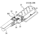
- FIG. 2 is a perspective view showing an appearance of an example of a transceiver module assembly and receptacle assembly according to the present invention, together with a printed wiring board.
- FIG. 3 is a perspective view showing an example of a transceiver module according to the present invention.
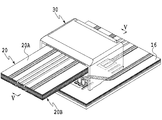
- FIG. 4 is a perspective view showing a part of a host connector and a wiring board used in an example of the receptacle assembly according to the present invention.
- FIG. 5 is a cross-sectional view taken along the line VV in FIG.
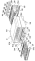
- FIG. 6 is a perspective view showing the appearance of an example of the high-speed signal connector according to the present invention.
- FIG. 7 is an exploded perspective view showing the configuration of the high-speed signal connector shown in FIG.
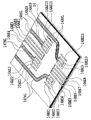
- FIG. 8 is a view showing an electrode portion and a conductor pattern of the printed wiring board shown in FIG.
- FIG. 9 is a perspective view showing a part of a host connector and a wiring board used in another example of the receptacle assembly according to the present invention.
- FIG. 10 is a diagram showing electrode portions and conductor patterns of the printed wiring board shown in FIG.
- FIG. 11A is a view showing an arrangement of contact pads on the connection end of the upper surface of the optical module substrate as a reference example.
- FIG. 11B is a diagram showing an arrangement of contact pads on the lower connection end facing the upper connection end of the optical module substrate shown in FIG. 11A.
- FIG. 12A is a perspective view including a partial cross section of the plug connector used in another example of the transceiver module according to the present invention and the configuration of the host connector to which the plug connector is connected. 12B is a cross-sectional view showing the configuration of the example shown in FIG. 12A together with the printed wiring board.
- FIG. 2 shows an example of a transceiver module assembly and receptacle assembly according to the invention together with a wiring board.
- the transceiver module assembly comprises a transceiver module (hereinafter also referred to as an optical module) 10 to which an optical connector 24 connected to one end of an optical fiber cable 14 as an optical cable is detachably connected, and an optical module
- the optical module receptacle assembly 12 to which 10 is connected is configured as a main element.
- the optical module 10 corresponds to, for example, a communication speed of 56 Gbs or more, and the optical module substrate 20 (see FIG. 4), the upper case 18 covering the upper portion of the optical module substrate 20, and the optical module substrate 20 And a lower case 22 covering the lower part of the lower case.
- the upper case 18 is formed of, for example, a metal material having excellent thermal conductivity, and has a recess (not shown) in which the upper portion of the optical module substrate 20 is accommodated. Through holes (not shown) communicating with the concave portion are formed in two places at predetermined intervals in the upper wall portion forming the concave portion. A small screw BS1 for fixing the upper case 18 to the optical module substrate 20 and the lower case 22 described later is inserted into each through hole.
- the lower case 22 is formed of, for example, a metal material having excellent thermal conductivity, and has a relatively shallow recess (not shown) in which the lower portion of the optical module substrate 20 is accommodated.
- the optical module substrate 20 supports a connector support member (not shown) that accommodates and supports a receptacle (not shown) to which the optical connector 24 is connected, supports the connector support member, and also has a light emitting / receiving element unit etc. It is comprised including the board part mounted in a mounting surface as a main element.
- the contact end of the substrate portion is a contact pad having a thickness of about 1 mm and comprising a plurality of contact pads formed in parallel to each other at a predetermined distance, as shown in an exaggerated manner in FIGS. 1A and 1B.
- the groups 20EA, 20EB are provided on the upper surface 20A and the lower surface 20B (see FIG. 5) at one end.
- Contact pad groups 20EA and 20EB are electrically connected to the conductor patterns in the substrate portion.
- the connection end portion of the substrate portion and the end portion provided with the above-described connector support member are electrically connected via a conductor formed inside.
- the contact pad group 20EA formed on the upper surface 20A at the connection end of the substrate portion is, for example, as shown in FIG. 1A, a contact pad 20A1 which is conducted to the ground line (G) sequentially from the end, Contact pads 20A2 and 20A3 conducting to the high speed signal line (S), a contact pad 20A4 conducting to the ground line (G), power contact pads 20A5 and 20A6 conducting to the power supply line, and a ground line (G) It comprises a contact pad 20A7 conducting, a contact pad 20A8 and 20A9 conducting to the high speed signal line (S) on the receiving side, a contact pad 20A10 conducting to the ground line (G), and a spare contact pad 20A11. ing. That is, the contact pad group 20EA is composed of eleven contact pads.
- the contact pad group 20EB formed on the lower surface 20B at the connection end of the substrate portion is, for example, as shown in FIG. 1B, a contact pad 20B1 which conducts sequentially to the ground line (G) from the end, Contact pads 20B2 and 20B3 conducting to the high speed signal line (S), contact pads 20B4 conducting to the ground line (G), and contact pads 20B5, 20B6 and 20B7 conducting to the low speed signal line (S), Contact pad 20B8 conducting to ground line (G), contact pad 20B9 conducting to high speed signal line (S) on the receiving side, 20B10, and contact pad 20B11 conducting to ground line (G) It is configured. That is, the contact pad group 20EB is configured of eleven contact pads. The contact pad group 20EB is biased to one side with respect to the above-mentioned contact pad group 20EA along the arrangement direction of the contact pads.
- the optical module receptacle assembly 12 is fixed on, for example, a printed wiring board 16 in a predetermined electronic device.
- the optical module receptacle assembly 12 includes a receptacle cage 15 forming an outer shell thereof, and a host connector 30 disposed in a host connector accommodating portion 15H formed in the receptacle cage 15 (see FIGS. 4 to 6). Is composed including.
- the receptacle cage 15 is formed of, for example, a metal material, and has a host connector housing portion 15H inside.
- the host connector housing portion 15H communicates with a module insertion port at one side of the receptacle cage 15.
- a space (module housing portion 15M) into which the connection end of the optical module 10 is inserted is formed between one end of the host connector 30 in the host connector housing portion 15H and one end of the plug insertion port.
- the host connector 30 corresponds to, for example, a communication speed of 56 Gbs or more, and a connector insulator having a slot 30SL into which the connection end of the optical module 10 is removably inserted, and a plurality of contact terminals 32ai, 36ai (i 1 to n and n are positive integers (see FIGS. 5 and 7).
- Each of the contact terminals 32ai and 36ai is to electrically connect the connection end of the optical module 10 to an electrode group connected to a conductor pattern of the printed wiring board 16 described later.
- the contact terminal 32ai is, as shown in FIGS. 5 and 7, a movable contact portion 32M having at one end a contact portion 32C to be in contact with the contact pads 20B1 to 20B11 at the connection end of the optical module 10; A fixed portion 32F having at one end a fixed terminal portion fixed by soldering to 16 electrode groups, and a connecting portion 32E connecting the other end of the movable contact portion 32M and the other end of the fixed portion 32F .
- the fixed terminal portion of the fixing portion 32F is directed in the insertion direction of the connection end portion of the optical module 10 along the X coordinate axis direction so as to be substantially parallel to the connecting portion 32E, as enlarged and shown in FIG. It is bent.
- the distance CH from the other end (curved portion) of the movable contact portion 32M to the mounting surface of the printed wiring board 16 is the printed wiring board 16 of the end portion 36fe of the slope portion in the fixed portion 36F of the contact terminal 36ai described later. It is set larger than the distance to the mounting surface.
- the Y coordinate axis is taken along the arrangement direction of the contact terminals 32 ai and 36 ai
- the X coordinate axis is taken along the attachment and detachment direction of the connection end of the optical module 10.
- the Z coordinate axis is orthogonal to the X coordinate axis and the Y coordinate axis.
- the contact terminal 36 ai is fixed by soldering to the electrode group of the printed wiring board 16 and the movable contact portion 36 M having at one end the contact portion 36 C to be in contact with the contact pads 20 A 1 to 20 A 11 at the connection end of the optical module 10 It comprises the fixed part 36F which has a terminal part at one end, and the connection part 36E which connects the other end of the movable contact part 36M and the other end of the fixed part 36F.
- the fixing terminal portion of the fixing portion 36F is bent in the insertion direction of the connection end portion of the optical module 10 so as to be substantially orthogonal to the connecting portion 36E, as enlarged and shown in FIG.
- the connector insulator is formed of a resin material, and has a slot 30SL through which the connection end of the optical module 10 passes when the optical module 10 is attached or detached.
- the slot 30SL has a maximum height of about 1.35 mm corresponding to the thickness of the connection end of the optical module 10.
- the periphery of the slot 30SL is formed to be surrounded by the side walls 30RS and 30LS and an upper portion 30T interconnecting the side walls 30RS and 30LS.
- the slot 30SL communicates with a connection end accommodating portion 30E into which the connection end of the optical module 10 is inserted.
- the minimum depth Dp in the connection end accommodating portion 30E is set to, for example, about 6.0 mm. As shown in FIG.
- a predetermined first chamfered portion C1 is applied to a portion forming the slot 30SL in the upper portion 30T of the connector insulator. Further, a predetermined second chamfered portion C2 is also applied to an end portion of the upper portion 30T of the connector insulator.
- the slit 30ASi is formed on the inner peripheral surface of the upper portion 30T, and the slit 30BSi is formed on the lower inner peripheral surface facing the slit 30ASi.
- the Y coordinate axis is taken along the arrangement direction of the contact terminals 32ai and 36ai
- the X coordinate axis is taken along the attachment and detachment direction of the connection end of the optical module 10.
- the Z coordinate axis is orthogonal to the X coordinate axis and the Y coordinate axis.
- the contact portion 36C of the movable contact portion 36M of the contact terminal 36ai and the contact portion 32C of the movable contact portion 32M of the contact terminal 32ai face each other. .
- the connection end of the optical module 10 is the movable contact of the contact terminal 36ai It is inserted between the contact portion 36C of the portion 36M and the contact portion 32C of the movable contact portion 32M of the contact terminal 32ai.
- the contact portion 36C of the movable contact portion 36M of each contact terminal 36ai abuts on the contact pad group 20EA, and the contact portion 32C of the movable contact portion 32M of each contact terminal 32ai abuts on the contact pad group 20EB.
- the maximum distance Lc from the open end face of the slot 30SL of the contact portion 36C of the movable contact portion 36M of each contact terminal 36ai and the contact portion 32C of the movable contact portion 32M of each contact terminal 32ai is set to about 3.0 mm at maximum. It is done.
- connection members 34A, 34B, 34E, and 34F connecting to each other are fitted in the recess 30R of the connector insulator.
- the connection members 34A, 34B, 34E, and 34F are arranged in a line along the Y coordinate axis in FIG. 5 in the recess 30R.
- the connecting members 34A, 34B, 34E, and 34F are each formed of, for example, a conductive resin, and the protrusions 34a, 34b, 34e, and 34f are in contact with the surface of the connecting portion 32E from below the connecting portion 32E. Have.
- connection members 38A, 38B which electrically connect the adjacent ground contact terminals 36ai to each other at the same potential, 38E and 38F are disposed parallel to one another along the Y coordinate axis in FIG. 5 (see FIG. 7).
- the connecting members 38A, 38B, 38E, and 38F integrally formed of conductive resin are disposed at predetermined intervals, and are protrusions that contact the surface of the movable contact portion 36M from above the movable contact portion 36M. It has sections 38a, 38b, 38e and 38f.
- a plurality of positioning pins 30D fitted to the positioning holes of the printed wiring board 16 are formed on the bottom of the connector insulator.
- the electrode group of the printed wiring board 16 to which the fixed terminal portion of the fixed portion 32F of the contact terminal 32ai and the fixed terminal portion of the fixed portion 36F of the contact terminal 36ai are fixed by soldering is partially illustrated in FIG. As shown in FIG. 1, it is formed at the end of the printed wiring board 16.
- the first electrode group consisting of the electrode parts 16BE1 to 16BE11 to which the fixed terminal part of the fixed part 32F of the contact terminal 32ai is soldered and fixed
- the fixed terminal part of the fixed part 36F of the contact terminal 36ai is soldered and fixed
- a second electrode group consisting of the electrode portions 16AE1 to 16AE11.
- the first electrode group is formed at a position close to the end of the printed wiring board 16, and the second electrode group is formed at a position farther from the end of the printed wiring board 16 than the first electrode group. It is formed.
- the electrode portions 16BE1 to 16BE11 in the first electrode group respectively include a contact pad 20B1 electrically connected to the ground line (G) formed on the lower surface 20B at the connection end of the above-mentioned substrate portion, and a high speed signal line Contact pads 20B2 and 20B3 conducting to S), contact pads 20B4 conducting to ground line (G), contact pads 20B5, 20B6 and 20B7 conducting to low speed control signal line (S), and ground line (G) And the contact pad 20B9 conductive to the high speed signal line (S) on the reception side, and 20B10, and the contact pad 20B11 conductive to the ground line (G).
- Electrodes 16BE2 and 16BE3 are each formed on the surface layer of printed wiring board 16 through conductor path 16THL passing a position separated from one end of the second electrode group, and another high-speed signal line (S) It is directly connected to the portion of the conductor pattern to be considered.
- the electrode portions 16BE9 and 16BE10 are formed on the surface layer of the printed wiring board 16 respectively, and other high-speed signal lines (via conductor paths 16RHL passing through a position separated from the other end of the second electrode group) It is directly connected to the portion of the conductor pattern to be S).
- the electrode portions 16AE1 to 16AE11 in the second electrode group respectively include a contact pad 20A1 electrically connected to the ground line (G) formed on the upper surface 20A at the connection end of the above-mentioned substrate portion, and a high speed signal line S) the contact pads 20A2 and A3 conducting to the ground line, the contact pad 20A4 conducting to the ground line (G), the power source contact pads 20A5 and 20A6 conducting to the power supply line, and the contact pad 20A7 conducting to the ground line (G)
- the contact pads 20A8 and 20A9 electrically connected to the high speed signal line (S) on the receiving side, the contact pads 20A10 electrically connected to the ground line (G), and the spare contact pad 20A11 are formed.
- the electrode portions 16AE2 and 16AE3 are directly connected to the portions of the conductor pattern to be another high-speed signal line (S) through the conductor path 16THL formed on the surface layer of the printed wiring board 16, respectively. Further, the electrode portions 16AE8 and 16AE9 are each directly formed on the surface layer of the printed wiring board 16 and directly connected to the portion of the conductor pattern to be another high-speed signal line (S) through the conductor path 16RHL. .
- FIG. 9 shows a part of a host connector and a wiring substrate used in another example of the receptacle assembly according to the present invention, together with the optical module substrate.
- the optical module receptacle assembly is fixed on, for example, a printed wiring board 56 in a predetermined electronic device.
- the optical module receptacle assembly includes a receptacle cage (not shown) forming an outer shell thereof and a host connector 30 'disposed in a host connector receptacle formed in the receptacle cage. .
- the host connector 30 ′ abuts on the connector insulator having a slot through which the connection end of the optical module substrate 20 passes and the lower surface 20B of the connection end A plurality of first contact terminals (not shown) and a second contact terminal (not shown) to be abutted to the upper surface 20A at the connection end.
- the configurations of the connector insulator and the second contact terminal are the same as the configurations of the insulator and the contact terminal 36ai shown in FIG.
- the first contact terminal is fixed by soldering to a movable contact portion having at one end a contact portion 32C to be in contact with the contact pads 20B1 to 20B11 at the connection end of the optical module 10, and an electrode group of the printed wiring board 56 It comprises: the fixed part which has a fixed terminal part in one end, and the connection part which connects the other end of a movable contact part, and the other end of fixed part.
- the fixed terminal portion in the fixed portion is bent in the direction in which the connection end of the optical module 10 is pulled out so as to be substantially parallel to the connection portion.
- the plurality of first contact terminals and the second contact terminals respectively electrically connect the connection end of the optical module substrate 20 to an electrode group connected to a conductor pattern of the printed wiring board 56 described later. Be done.
- the first electrode group including the electrode portions 56BE1 to 56BE11 to which the fixed terminal portion in the fixed portion of the first contact terminal is soldered and fixed, and the fixed terminal portion in the fixed portion of the second contact terminal are soldered
- a second electrode group consisting of the electrode parts 56AE1 to 56AE11 to be attached and fixed.
- a ground conductor 56G is formed between the first electrode group and the second electrode group on the mounting surface of the printed wiring board 56 so as to separate the first electrode group and the second electrode group. It is done. The formation of the ground conductor 56G connected to the ground line via the via in this manner further improves the crosstalk characteristic of the host connector 30 '.
- the first electrode group described above is formed at a position close to the end of the printed wiring board 56, and the second electrode group described above is from the end of the printed wiring board 56 more than the first electrode group. It is formed at a distant position.
- the electrode portions 56BE1 to 56BE11 in the first electrode group respectively transmit the contact pads 20B1 electrically connected to the ground line (G) formed on the lower surface 20B at the connection end of the substrate portion of the optical module substrate 20 described above, and Contact pads 20B2 and 20B3 conducting to the high speed signal line (S) on the side, a contact pad 20B4 conducting to the ground line (G), and contact pads 20B5, 20B6 and 20B7 conducting to the low speed control signal line (S) , Contact pad 20B8 conducting to the ground line (G), contact pad 20B9 conducting to the high speed signal line (S) on the receiving side, and 20B10, and contact pad 20B11 conducting to the ground line (G) It is formed.
- the electrode portions 56BE2 and 56BE3 are connected to portions of the conductor patterns 56THL2 to be high-speed signal lines (S) through the conductor paths 56THL1 and the vias 56VIA, respectively.
- One end of each conductor path 56THL1 is connected to the electrode portions 56BE2 and 56BE3 through the via 56VIA located adjacent to the electrode portions 56BE2 and 56BE3, and the other end of each conductor path 56THL1 is a position adjacent to each conductor pattern 56THL2 Are connected to the conductor patterns 56THL2 through the vias 56VIA.
- Each conductor path 56THL1 is formed in the lower layer below the ground conductor 56G formed on the surface layer of the printed wiring board 56, as shown by a broken line in FIG.
- the electrode portions 56BE9 and 56BE10 are connected to portions of a conductor pattern 56RHL2 which is a high-speed signal line (S) through the conductor paths 56RHL1 and vias 56VIA, respectively.
- One end of conductor path 56RHL1 is connected to electrode portions 56BE9 and 56BE10 through via 56VIA located adjacent to electrode portions 56BE9 and 56BE10, and the other end of conductor path 56RHL1 is located adjacent to conductor pattern 56RHL2
- Each conductor pattern 56THL2 is connected through 56VIA.
- Each conductor path 56RHL1 is formed in a lower layer below the ground conductor 56G formed on the surface layer of the printed wiring board 56, as shown by a broken line in FIG.
- the electrode parts 56AE1 to 56AE11 in the second electrode group respectively include a contact pad 20A1 electrically connected to the ground line (G) formed on the upper surface 20A at the connection end of the above-mentioned substrate part, and a high speed signal line S) the contact pads 20A2 and A3 conducting to the ground line, the contact pad 20A4 conducting to the ground line (G), the power source contact pads 20A5 and 20A6 conducting to the power supply line, and the contact pad 20A7 conducting to the ground line (G)
- the contact pads 20A8 and 20A9 electrically connected to the high speed signal line (S) on the receiving side, the contact pads 20A10 electrically connected to the ground line (G), and the spare contact pad 20A11 are formed.
- the electrode portions 56AE2 and 56AE3 are directly connected to the portions of the conductor pattern to be another high-speed signal line (S) through the conductor paths 56THL formed on the surface layer of the printed wiring board 56, respectively. Also, the electrode portions 56AE8 and 56AE9 are respectively formed directly on the surface layer of the printed wiring board 56 and directly connected to the portions of the conductor pattern to be another high-speed signal line (S) through the conductor paths 56RHL. .
- the optical module substrate 20 used in one example of the transceiver module according to the present invention can increase the number of channels as compared with the optical module substrate 40 as a reference example shown in FIGS. 11A and 11B described later.
- the structure and conductor pattern of the printed wiring board 16 used in an example of the receptacle assembly according to the present invention shown in FIG. 8 correspond to the arrangement of the contact pads of the optical module substrate 20 while maintaining the vias and the like. Since it is manufactured without using it, it is simplified as compared with the conductor pattern of the printed wiring board 56 shown in FIG.
- FIGS. 11A and 11B schematically show a reference example of the optical module substrate 40 in the optical module which is attachable to and detachable from the above-mentioned host connectors 30 and 30 ′.
- An optical module substrate 40 in the optical module supports a connector support member (not shown) that accommodates and supports a receptacle (not shown) to which the optical connector is connected, and supports the connector support member and also emits light / light receiving element
- a unit etc. is comprised including the board
- connection end portion of the substrate portion is, as shown in an exaggerated manner in FIGS. 11A and 11B, a contact pad group 40EA, 40EB consisting of a plurality of contact pads formed in parallel with each other at a predetermined interval, 40A and the lower surface 40B.
- the contact pad groups 40EA and 40EB are each electrically connected to the conductor pattern in the substrate portion.
- the connection end portion of the substrate portion and the end portion provided with the above-described connector support member are electrically connected via a conductor formed inside.
- the contact pad group 40EA formed on the upper surface 40A at the connection end of the substrate portion is, for example, as shown in FIG. 11A, a contact pad 40A1 conducted to the ground line (G) sequentially from the end, Contact pads 40A2 and 40A3 conducting to the high-speed signal line (S), contact pads 40A4 conducting to the ground line (G), power contact pads 40A5 and 40A6 conducting to the power supply line, and the ground line (G)
- the contact pad 40A7 is conductive, the contact pads 40A8 and 40A9 conductive to the high speed signal line (S) on the reception side, and the contact pad 40A10 conductive to the ground line (G). That is, the contact pad group 40EA is composed of ten contact pads.
- the contact pad group 40EB formed on the lower surface 40B at the connection end of the substrate portion is, for example, as shown in FIG. 11B, the contact pad 40B1 which conducts sequentially to the ground line (G) from the end, and low speed control Contact pads 40B2 and 40B3 conducting to the signal line (S), contact pads 40B4, 40B5 and 40B6 conducting to the slow control signal line (S), and a contact pad 40B7 conducting to the slow control signal line (S) 40B8 and contact pads 40B9 and 40B10 electrically connected to the ground line (G). That is, the contact pad group 40EB is configured of ten contact pads.
- 20B6, and 20B7, and the contact pads 40B4, 40B5, and 40B6 can be electrically connected to the electrode portions 16BE5, 16BE6, and 16BE7 through the contact terminals 32ai, respectively.
- the optical module substrate 40 having a smaller number of channels than the module substrate 20 can be connected to the above-described host connectors 30 and 30 '.
- connection ends of the substrate portion of the optical module substrate 20 used in one example of the above-described transceiver module assembly according to the present invention are a plurality of contact pads formed parallel to each other at a predetermined distance.
- the contact pads 20EA and 20EB at one end on the upper surface 20A and the lower surface 20B are not limited to such an example.
- the connection end of the substrate portion 60 may be connected to the plug connector 62.
- the contact pads 60Ei are arranged at predetermined intervals in a row in a direction substantially orthogonal to the insertion direction of the module substrate 60 with respect to the plug connector 62.
- the arrangement of contact pads 60Ei on the front and back sides may be identical to the arrangement of contact pads 20EA and contact pads 20EB as shown in, for example, FIGS.
- the arrangement of the contact pads 60Ei on the back surface includes a pair of contact pads conductive to at least the high speed signal line (S) on the transmission side and a pair of contact pads conductive to the high speed signal line (S) on the reception side. It may be configured as follows.
- connection end 62PE is inserted into a slot of a host connector 70 described later.
- the connection end 62PE has a recess 62R in which the end of the module substrate 60 is inserted.
- the recess 62R is in communication with the open end of the substrate support.
- the both sides in the recessed part 62R are formed of the side wall part.
- grooves 62Rg for guiding the side portion of the module substrate 60 are formed on both side walls forming the recess 62R so as to keep the posture of the module substrate 60 parallel to the upper surface of the connection end 62PE.
- the substrate support of the plug connector 62 has an open end through which the end of the inserted module substrate 60 passes.
- a pair of positioning portions 16A that are in contact with the substrate support wall (not shown) in the upper case and the lower case of the optical module are formed separately from each other.
- an elongated spring portion 62B is formed to be in contact with a substrate support wall (not shown) in the upper case and the lower case.
- the contact terminals 62EAi are arranged on the top surface of the connection end 62PE facing the pair of positioning portions 62A of the substrate support portion with a predetermined interval corresponding to the above-mentioned contact pad 60Ei.
- the contact terminal 62EAi includes, for example, a power supply terminal, a signal contact terminal, and a grounding contact terminal. For example, a pair of adjacent signal contact terminals is disposed between the ground contact terminals.
- the contact terminal 62EAi has a fixed terminal portion soldered and fixed to the contact pad 60Ei, and a contact portion to be in contact with the contact portion of the contact terminal 74ai of the host connector 70.
- the contact terminals 62EBi are arranged on the lower surface of the connection end 62PE facing the spring portion 62B of the substrate support portion at a predetermined interval corresponding to the above-mentioned contact pad 60Ei.
- the contact terminal 62EBi includes, for example, a power supply terminal, a signal contact terminal, and a grounding contact terminal. For example, a pair of adjacent signal contact terminals is disposed between the ground contact terminals.
- the contact terminal 62EBi has a fixed terminal portion soldered and fixed to the contact pad 60Ei, and a contact portion abutted against the contact portion of the contact terminal 72ai of the host connector 70.
- Each of the contact terminals 72ai and 74ai electrically connects the connection end 62PE of the plug connector 62 to an electrode group connected to a conductor pattern of the printed wiring board 76 described later.
- the contact terminal 72ai is, as shown in FIG. 12B, a movable contact portion 72M having at one end a contact portion 72C to be in contact with the contact terminal 62EBi at the connection end 62PE of the plug connector 62, and an electrode group of the printed wiring board 76 And a connecting portion 72E for connecting the other end of the movable contact portion 72M and the other end of the fixed portion 72F.
- the fixed terminal portion of the fixing portion 72F is bent in the insertion direction of the connection end 62PE of the plug connector 62 along the X coordinate axis direction so as to be substantially parallel to the connecting portion 72E.
- the Y coordinate axis is taken along the arrangement direction of the contact terminals 72ai and 74ai, and the X coordinate axis is taken along the attachment and detachment direction of the connection end 62PE of the plug connector 62.
- the Z coordinate axis is orthogonal to the X coordinate axis and the Y coordinate axis.
- the contact terminal 74 ai is a movable contact 74 M having at one end a contact portion 74 C that contacts the contact terminal 62 EAi at the connection end 62 PE of the plug connector 62, and a fixed terminal soldered to the electrode group of the printed wiring board 76. It comprises the fixed part 74F which has a part at one end, and the connection part 74E which connects the other end of the movable contact part 74M and the other end of the fixed part 74F.
- the fixed terminal portion of the fixing portion 74F is bent in the insertion direction of the connection end 62PE of the plug connector 62 so as to be substantially orthogonal to the connecting portion 74E.
- the movable contact portion 74M extends substantially parallel to the mounting surface of the printed wiring board 76, and the connecting portion 74E is bent from the end of the movable contact portion 74M so as to be substantially perpendicular to the mounting surface of the printed wiring board 76 It is done.
- the connector insulator is formed of a resin material and has a slot through which the connection end 62 PE of the plug connector 62 passes when the optical module is attached or detached.
- the slot has a maximum height corresponding to the thickness of the connection end 62 PE of the plug connector 62.
- the periphery of the slot is formed to be surrounded by the side wall portion and the upper portion interconnecting the both side wall portions.
- the slot communicates with a connection end accommodating portion 70E in which the connection end 62PE of the plug connector 62 is inserted.
- a plurality of slits 70ASi and 70BSi (i 1 to n, n is a positive integer) formed at predetermined intervals along the Y coordinate axis shown in FIG. 12B.
- the slit 70ASi is formed on the upper inner circumferential surface
- the slit 70BSi is formed on the lower inner circumferential surface facing the slit 70ASi.
- the contact portion 72C of the movable contact portion 72M of the contact terminal 72ai and the contact portion 74C of the movable contact portion 74M of the contact terminal 74ai are disposed to face each other.
- the connection end 62PE of the plug connector 62 is inserted into the connection end accommodating portion 70E via the slot as shown in FIG. 12B, the connection end 62PE of the plug connector 62 is a movable contact of the contact terminal 72ai. It is inserted between the contact portion 72C of the portion 72M and the contact portion 74C of the movable contact portion 74M of the contact terminal 74ai.
- the heat sink is provided on the receptacle cage 15 so as to dissipate the heat generated from the optical module 10 through the heat sink (not shown).
Abstract
In this invention, a contact pad group (20EB), which is formed on the bottom surface (20B) of a connection end section in the base portion of an optical module board (20), is constituted by including, sequentially from one edgemost part, a contact pad (20B1) which establishes a conductive connection to a ground line (G), contact pads (20B2) and (20B3) which establish a conductive connection to a high-speed signal line (S) on the sending side, a contact pad (20B4) which establishes a conductive connection to the ground line (G), contact pads (20B5, 20B6 and, 20B7) which establish conductive connections to a low-speed signal line (S), a contact pad (20B8) which establishes a conductive connection to the ground line (G), contact pads (20B9 and 20B10) which establish a conductive connection to a high-speed signal line (S) on the receiving side, and a contact pad (20B11) which establishes a conductive connection to the ground line (G). In a host connector (30), fixed terminal parts from a plurality of contact terminals (32ai) to be connected to the contact pads (20B2 and 20B3) which establish a conductive connection to the high-speed signal line (S) on the sending side and the contact pads (20B9 and 20B10) which establish a conductive connection to the high-speed signal line (S) on the receiving side are connected electrically, via an electrode part (16BE2), an electrode part (16BE3), an electrode part (16BE9), and an electrode part (16BE10) in a printed wiring board (16), to conductor paths (16THL, 16RHL) which continue into a high-speed signal line formed on a plane that is common to the electrode part (16BE2), the electrode part (16BE3), the electrode part (16BE9), and the electrode part (16BE10).
Description
本発明は、高速信号用コネクタ、および、それを備えるリセプタクルアセンブリ、トランシーバモジュールアセンブリに関する。
The present invention relates to a high speed signal connector, a receptacle assembly including the same, and a transceiver module assembly.
光通信システムにおいては、光ファイバ、もしくは、カッパケーブル、および、光コネクタ等により伝送される光信号をマザーボードに伝送するためにトランシーバモジュール、および、リセプタクルアセンブリが実用に供されている。トランシーバモジュール(特許文献1においてはSFPモジュールと呼称される)は、例えば、特許文献1に示されるように、プリント配線板に配されるリセプタクルアセンブリの一部を構成するケージに対し着脱可能とされる。そのようなトランシーバモジュールは、例えば、送信用光サブアセンブリ(以下、TOSA:Transmitting Optical Sub-Assemblyともいう)と、受信用光サブアセンブリ(以下、ROSA:Receiving Optical Sub-Assemblyともいう)と、TOSAおよびROSAための信号処理および制御等を行うモジュール基板と、モジュール基板をリセプタクルアセンブリにおけるホストコネクタに電気的に接続するモジュール基板の接続端子部と、を主な要素として含んで構成されている。モジュール基板の接続端子部は、例えば、特許文献2に示されるように、上述のホストコネクタとしてのSFP(Small Form-Factor Pluggable)コネクタを介してマザーボードに電気的に接続されている。SFPコネクタは、ケージにおけるトランシーバモジュールが通過する開口端部に向って開口するスロットをハウジングの端部に有している。モジュール基板の接続端子部は、スロットを介してハウジング内に着脱可能に挿入される。SFPコネクタのハウジング内には、各接点部がモジュール基板の接続端子部を挟持するように向き合って配置された第1のコンタクト端子列、および、第2のコンタクト端子列が設けられている。第1のコンタクト端子列、および、第2のコンタクト端子列は、それぞれ、モジュール基板の接続端子部の着脱方向に対し略直交するように所定の間隔をもってコンタクト端子が配置されている。第1のコンタクト端子列、および、第2のコンタクト端子列は、例えば、10本のコンタクト端子で構成されている。これにより、第1のコンタクト端子列、および、第2のコンタクト端子列における接点部は、それぞれ、挿入されたモジュール基板の接続端子部の上部コンタクトパッド列および下部コンタクトパッド列に電気的に接続される。
In the optical communication system, a transceiver module and receptacle assembly are put into practical use to transmit an optical signal transmitted by an optical fiber or copper cable, an optical connector or the like to a motherboard. A transceiver module (referred to as an SFP module in Patent Document 1) is, for example, removable from a cage which constitutes a part of a receptacle assembly disposed on a printed wiring board as disclosed in Patent Document 1 Ru. Such transceiver modules include, for example, a transmitting optical subassembly (hereinafter also referred to as TOSA: Transmitting Optical Sub-Assembly), a receiving optical subassembly (hereinafter also referred to as ROSA: Receiving Optical Sub-Assembly), and TOSA. And a module substrate for signal processing and control for ROSA, and a connection terminal portion of the module substrate for electrically connecting the module substrate to a host connector in the receptacle assembly as main elements. For example, as shown in Patent Document 2, the connection terminal portion of the module substrate is electrically connected to the mother board via a small form-factor pluggable (SFP) connector as the above-mentioned host connector. The SFP connector has a slot at the end of the housing that opens towards the open end of the cage through which the transceiver module passes. The connection terminal portion of the module substrate is removably inserted into the housing through the slot. In the housing of the SFP connector, a first contact terminal row and a second contact terminal row are provided in which the respective contact portions face each other so as to sandwich the connection terminal portion of the module substrate. In the first contact terminal row and the second contact terminal row, the contact terminals are arranged at predetermined intervals so as to be substantially orthogonal to the mounting and demounting direction of the connection terminal portion of the module substrate. The first contact terminal row and the second contact terminal row are constituted of, for example, ten contact terminals. Thereby, the contact portions in the first contact terminal row and the second contact terminal row are electrically connected to the upper contact pad row and the lower contact pad row of the connection terminal portion of the inserted module substrate, respectively. Ru.
近年、光通信システムにおいては、25Gbs以上のデータ伝送速度に対応するトランシーバモジュール、および、リセプタクルアセンブリを実現すべく開発が進められている。
In recent years, in optical communication systems, development is underway to realize transceiver modules and receptacle assemblies that support data transmission rates of 25 Gbs or more.
しかしながら、上述したような従来の規格に準拠したSFPコネクタにおいては、25Gbs以上のデータ伝送速度(通信速度)に対応した高速信号特性を得ることにも限界があるとともに、高周波数帯域の信号のチャンネル数を増大させることにも限界がある。その際、25Gbs以上のデータ伝送速度に対応したトランシーバモジュール、および、リセプタクルアセンブリは、10Gbs規格のトランシーバモジュールから25Gbs規格のトランシーバモジュールへの移行期において、旧式の通信システムにおける10Gbs規格の光ファイバ、もしくは、カッパケーブル、および、光コネクタ等にも接続するために10Gbs規格のトランシーバモジュール、および、リセプタクルアセンブリにも接続可能であることが要望される。
However, in the SFP connector based on the conventional standard as described above, there is a limit to obtaining high-speed signal characteristics corresponding to a data transmission rate (transmission rate) of 25 Gbs or more, and a channel of a high frequency band signal There is also a limit to increasing the number. At that time, transceiver modules and receptacle assemblies that support data transmission rates of 25 Gbs or higher are 10 Gbs standard optical fibers in old communication systems, or in transition from 10 Gbs transceiver modules to 25 Gbs transceiver modules. It is also desired that the 10 Gbs standard transceiver module and receptacle assembly be connectable to connect to Kappa cables, optical connectors, etc.
以上の問題点を考慮し、本発明は、高速信号用コネクタ、および、それを備えるリセプタクルアセンブリ、トランシーバモジュールアセンブリであって、比較的高周波数帯域の信号の伝送に対応できるとともに高周波数帯域の信号のチャンネル数を増大させることができ、しかも、高周波数帯域の異なる規格のトランシーバモジュールにも接続できる高速信号用コネクタ、および、それを備えるリセプタクルアセンブリ、トランシーバモジュールアセンブリを提供することを目的とする。
In view of the above problems, the present invention provides a connector for high-speed signals, a receptacle assembly including the same, and a transceiver module assembly, which can cope with the transmission of signals in a relatively high frequency band and is a signal in a high frequency band. It is an object of the present invention to provide a connector for high-speed signals which can increase the number of channels and can also connect to transceiver modules of different standards of high frequency band, and a receptacle assembly and transceiver module assembly including the same.
上述の目的を達成するために、本発明に係る高速信号用コネクタは、光モジュール用基板の接続端部における一方の電極面に接続される第1のコンタクト端子群と、光モジュール用基板の接続端部における一方の電極面に向かい合う他方の電極面に接続される第2のコンタクト端子群とを有する接続端部収容部を備えるハウジングを備え、第1のコンタクト端子群は、低速制御信号ライン群に導通する複数のコンタクト端子列の両脇に、それぞれ、接地用コンタクト端子を介して隣接した送信側の一対の高速信号ラインに導通する一対のコンタクト端子、受信側の一対の高速信号ラインに導通する一対のコンタクト端子、接地用コンタクト端子を含むことを特徴とする。
In order to achieve the above-mentioned object, the connector for high-speed signals according to the present invention comprises a connection between a first contact terminal group connected to one electrode surface at a connection end of an optical module substrate and the optical module substrate. A housing comprising a connection end accommodating portion having a second contact terminal group connected to the other electrode surface facing one electrode surface at the end, the first contact terminal group comprising a low speed control signal line group On both sides of a plurality of contact terminal rows that are electrically connected to each other, to a pair of contact terminals that are electrically connected to a pair of high speed signal lines on the transmission side adjacent via a ground contact terminal, and to a pair of high speed signal lines on a reception side A pair of contact terminals, and a ground contact terminal.
また、第1のコンタクト端子群の一部を構成する隣接した複数の接地用コンタクト端子の相互間は、複数の接続部材により電気的に同一電位に接続されてもよい。第1のコンタクト端子群および第2のコンタクト端子群は、それぞれ、11個のコンタクト端子により構成されてもよい。
In addition, the plurality of adjacent contact terminals that form part of the first contact terminal group may be electrically connected to the same potential by a plurality of connection members. Each of the first contact terminal group and the second contact terminal group may be configured by eleven contact terminals.
さらに、第1のコンタクト端子群を構成するコンタクト端子の固定端子部が、光モジュール用基板の接続端部のハウジングの接続端部収容部に対する挿入方向に向けて折り曲げられて形成される場合、少なくとも一対のコンタクト端子の固定端子部は、ハウジングが固定される配線基板における第2のコンタクト端子群が電気的に接続される導体路に隣接して形成される高速信号用導体路の端部に直接的に接続されてもよい。また、光モジュール用基板の端部は、プラグコネクタに接続されてもよい。
Furthermore, at least the fixed terminal portion of the contact terminal constituting the first contact terminal group is bent in the insertion direction with respect to the connection end storage portion of the housing of the connection end portion of the optical module substrate. The fixed terminal portions of the pair of contact terminals are directly connected to the end portion of the high-speed signal conductor path formed adjacent to the conductor path to which the second contact terminal group in the wiring substrate to which the housing is fixed is electrically connected. May be connected. Also, the end of the optical module substrate may be connected to the plug connector.
第1のコンタクト端子群を構成するコンタクト端子の可動接点部の他端のハウジングが固定される配線基板の実装面に対する位置が、第2のコンタクト端子群を構成するコンタクト端子の固定部における斜面部の端部のハウジングが固定される配線基板の実装面に対する位置よりも実装面に対し離隔してもよい。
The position of the other end of the movable contact portion of the contact terminal constituting the first contact terminal group with respect to the mounting surface of the wiring board to which the housing is fixed is a slope portion of the fixing portion of the contact terminal constituting the second contact terminal group The housing at the end of the housing may be separated from the mounting surface rather than the position relative to the mounting surface of the wiring board to which the housing at the end is fixed.
本発明に係るリセプタクルアセンブリは、光モジュール用基板を備えるトランシーバモジュールと接続される上述の高速信号用コネクタと、トランシーバモジュールが通過するモジュールスロットを一端に有し、トランシーバモジュールを着脱可能に収容するモジュール収容部と、モジュール収容部に連通し、高速信号用コネクタを収容するコネクタ収容部と、を有するリセプタクル用ケージと、を備えて構成される。
A receptacle assembly according to the present invention has a connector for high-speed signals described above connected to a transceiver module having an optical module substrate, and a module slot having a module slot through which the transceiver module passes, and removably accommodating the transceiver module. And a receptacle cage having a receptacle and a connector receptacle communicating with the module receptacle and containing the high-speed signal connector.
本発明に係るトランシーバモジュールアセンブリは、低速制御信号ライン群の両脇に、それぞれ、接地用ラインを介して隣接した送信側の一対の高速信号ラインと、受信側の一対の高速信号ラインと、接地用ラインとを一方の電極面に有する光モジュール用基板を備えるトランシーバモジュールと、トランシーバモジュールと接続される高速信号用コネクタと、トランシーバモジュールが通過するモジュールスロットを一端に有し、トランシーバモジュールを着脱可能に収容するモジュール収容部と、モジュール収容部に連通し、高速信号用コネクタを収容するコネクタ収容部と、を有するリセプタクル用ケージと、を備えるリセプタクルアセンブリと、を備えて構成される。
The transceiver module assembly according to the present invention comprises, on both sides of the low speed control signal line group, a pair of high speed signal lines on the transmission side adjacent to each other via the ground line, a pair of high speed signal lines on the reception side, Transceiver module having an optical module substrate having an interconnect line on one electrode surface, a high-speed signal connector connected to the transceiver module, and a module slot at one end through which the transceiver module passes And a receptacle cage having a module housing portion housed in the connector housing portion and a connector housing portion communicating with the module housing portion and housing the high speed signal connector.
本発明に係るトランシーバモジュールは、光コネクタに接続され、低速制御信号ライン群の両脇に、それぞれ、接地用ラインを介して隣接した送信側の一対の高速信号ラインと、受信側の一対の高速信号ラインと、接地用ラインとを一方の電極面に有する光モジュール用基板と、光モジュール用基板の上部を覆うアッパーケース、および、光モジュール用基板の下部を覆うロアケースと、を備えて構成される。
The transceiver module according to the present invention is connected to the optical connector, and on both sides of the low speed control signal line group, a pair of transmitting high speed signal lines adjacent to each other via the grounding line, and a pair of high speed receiving side The optical module substrate having the signal line and the grounding line on one electrode surface, an upper case covering the upper portion of the optical module substrate, and a lower case covering the lower portion of the optical module substrate Ru.
本発明に係る高速信号用コネクタ、および、それを備えるリセプタクルアセンブリ、トランシーバモジュールアセンブリによれば、第1のコンタクト端子群は、低速制御信号ライン群に導通する複数のコンタクト端子列の両脇に、それぞれ、接地用コンタクト端子を介して隣接した送信側の一対の高速信号ラインに導通する一対のコンタクト端子、受信側の一対の高速信号ラインに導通する一対のコンタクト端子、接地用コンタクト端子を含むので比較的高周波数帯域の信号の伝送に対応できるとともに高周波数帯域の信号のチャンネル数を増大させることができ、しかも、高周波数帯域の異なる規格のトランシーバモジュールにも接続できる。
According to the connector for high-speed signals according to the present invention, and the receptacle assembly and transceiver module assembly including the same, the first contact terminal group is disposed on both sides of the plurality of contact terminal rows conducting to the low-speed control signal line group. Each includes a pair of contact terminals electrically connected to a pair of high speed signal lines on the transmission side adjacent to each other via a ground contact terminal, a pair of contact terminals electrically connected to a pair of high speed signal lines on a reception side, and a ground contact terminal. It is possible to cope with transmission of signals in relatively high frequency bands, increase the number of channels of signals in high frequency bands, and connect to transceiver modules of different standards in high frequency bands.
図2は、本発明に係るトランシーバモジュールアセンブリおよびリセプタクルアセンブリの一例を、配線基板とともに示す。
FIG. 2 shows an example of a transceiver module assembly and receptacle assembly according to the invention together with a wiring board.
図2および図3において、トランシーバモジュールアセンブリは、光ケーブルとしての光ファイバケーブル14の一端に接続される光コネクタ24が着脱可能に接続されるトランシーバモジュール(以下、光モジュールともいう)10と、光モジュール10が接続される光モジュール用リセプタクルアセンブリ12と、を主な要素として構成されている。
2 and 3, the transceiver module assembly comprises a transceiver module (hereinafter also referred to as an optical module) 10 to which an optical connector 24 connected to one end of an optical fiber cable 14 as an optical cable is detachably connected, and an optical module The optical module receptacle assembly 12 to which 10 is connected is configured as a main element.
光モジュール10は、例えば、56Gbs以上の通信速度に対応するものとされ、光モジュール用基板20(図4参照)と、光モジュール用基板20の上部を覆うアッパーケース18と、光モジュール用基板20の下部を覆うロアケース22とを含んで構成されている。
The optical module 10 corresponds to, for example, a communication speed of 56 Gbs or more, and the optical module substrate 20 (see FIG. 4), the upper case 18 covering the upper portion of the optical module substrate 20, and the optical module substrate 20 And a lower case 22 covering the lower part of the lower case.
アッパーケース18は、例えば、熱伝導性の優れた金属材料で成形され、光モジュール用基板20の上部が収容される凹部(不図示)を有している。凹部を形成する上壁部には、その凹部に連通する透孔(不図示)が所定の間隔で2箇所に形成されている。各透孔には、アッパーケース18を光モジュール用基板20および後述するロアケース22に固定するための小ネジBS1が挿入される。ロアケース22は、例えば、熱伝導性の優れた金属材料で成形され、光モジュール用基板20の下部が収容される比較的浅い凹部(不図示)を有している。
The upper case 18 is formed of, for example, a metal material having excellent thermal conductivity, and has a recess (not shown) in which the upper portion of the optical module substrate 20 is accommodated. Through holes (not shown) communicating with the concave portion are formed in two places at predetermined intervals in the upper wall portion forming the concave portion. A small screw BS1 for fixing the upper case 18 to the optical module substrate 20 and the lower case 22 described later is inserted into each through hole. The lower case 22 is formed of, for example, a metal material having excellent thermal conductivity, and has a relatively shallow recess (not shown) in which the lower portion of the optical module substrate 20 is accommodated.
光モジュール用基板20は、光コネクタ24が接続されるレセプタクル(不図示)を内部に収容し支持するコネクタ支持部材(不図示)と、そのコネクタ支持部材を支持するとともに発光/受光素子ユニット等が実装面に実装される基板部とを主な要素として含んで構成されている。
The optical module substrate 20 supports a connector support member (not shown) that accommodates and supports a receptacle (not shown) to which the optical connector 24 is connected, supports the connector support member, and also has a light emitting / receiving element unit etc. It is comprised including the board part mounted in a mounting surface as a main element.
その基板部の接続端部は、図1Aおよび図1Bに誇張拡大して示されるように、約1mmの厚みを有し、所定の間隔で互いに平行に形成される複数のコンタクトパッドからなるコンタクトパッド群20EA、20EBを一端の上面20Aおよび下面20B(図5参照)に有している。また、コンタクトパッド群20EA、および、20EBは、基板部内の導体パターンに電気的に接続されている。基板部の接続端部と上述のコネクタ支持部材が設けられる端部とは、内部に形成される導体を介して電気的に接続されている。
The contact end of the substrate portion is a contact pad having a thickness of about 1 mm and comprising a plurality of contact pads formed in parallel to each other at a predetermined distance, as shown in an exaggerated manner in FIGS. 1A and 1B. The groups 20EA, 20EB are provided on the upper surface 20A and the lower surface 20B (see FIG. 5) at one end. Contact pad groups 20EA and 20EB are electrically connected to the conductor patterns in the substrate portion. The connection end portion of the substrate portion and the end portion provided with the above-described connector support member are electrically connected via a conductor formed inside.
基板部の接続端部における上面20Aに形成されるコンタクトパッド群20EAは、例えば、図1Aに示されるように、一番端から順次、グランドライン(G)に導通するコンタクトパッド20A1と、送信側の高速信号ライン(S)に導通するコンタクトパッド20A2および20A3と、グランドライン(G)に導通するコンタクトパッド20A4と、電源ラインに導通する電源用コンタクトパッド20A5および20A6と、グランドライン(G)に導通するコンタクトパッド20A7と、受信側の高速信号ライン(S)に導通するコンタクトパッド20A8および20A9と、グランドライン(G)に導通するコンタクトパッド20A10と、予備用コンタクトパッド20A11とを含んで構成されている。即ち、コンタクトパッド群20EAは、11個のコンタクトパッドから構成されている。
The contact pad group 20EA formed on the upper surface 20A at the connection end of the substrate portion is, for example, as shown in FIG. 1A, a contact pad 20A1 which is conducted to the ground line (G) sequentially from the end, Contact pads 20A2 and 20A3 conducting to the high speed signal line (S), a contact pad 20A4 conducting to the ground line (G), power contact pads 20A5 and 20A6 conducting to the power supply line, and a ground line (G) It comprises a contact pad 20A7 conducting, a contact pad 20A8 and 20A9 conducting to the high speed signal line (S) on the receiving side, a contact pad 20A10 conducting to the ground line (G), and a spare contact pad 20A11. ing. That is, the contact pad group 20EA is composed of eleven contact pads.
基板部の接続端部における下面20Bに形成されるコンタクトパッド群20EBは、例えば、図1Bに示されるように、一番端から順次、グランドライン(G)に導通するコンタクトパッド20B1と、送信側の高速信号ライン(S)に導通するコンタクトパッド20B2および20B3と、グランドライン(G)に導通するコンタクトパッド20B4と、低速信号ライン(S)に導通するコンタクトパッド20B5、20B6、および、20B7と、グランドライン(G)に導通するコンタクトパッド20B8と、受信側の高速信号ライン(S)に導通するコンタクトパッド20B9、および、20B10と、グランドライン(G)に導通するコンタクトパッド20B11と、を含んで構成されている。即ち、コンタクトパッド群20EBは、11個のコンタクトパッドから構成されている。コンタクトパッド群20EBは、コンタクトパッドの配列方向に沿って上述のコンタクトパッド群20EAに対し一方に偏倚している。
The contact pad group 20EB formed on the lower surface 20B at the connection end of the substrate portion is, for example, as shown in FIG. 1B, a contact pad 20B1 which conducts sequentially to the ground line (G) from the end, Contact pads 20B2 and 20B3 conducting to the high speed signal line (S), contact pads 20B4 conducting to the ground line (G), and contact pads 20B5, 20B6 and 20B7 conducting to the low speed signal line (S), Contact pad 20B8 conducting to ground line (G), contact pad 20B9 conducting to high speed signal line (S) on the receiving side, 20B10, and contact pad 20B11 conducting to ground line (G) It is configured. That is, the contact pad group 20EB is configured of eleven contact pads. The contact pad group 20EB is biased to one side with respect to the above-mentioned contact pad group 20EA along the arrangement direction of the contact pads.
光モジュール用リセプタクルアセンブリ12は、例えば、所定の電子機器内のプリント配線基板16上に固定されている。光モジュール用リセプタクルアセンブリ12は、その外郭部を形成するリセプタクル用ケージ15と、リセプタクル用ケージ15内に形成されるホストコネクタ収容部15Hに配されるホストコネクタ30と(図4乃至図6参照)を含んで構成されている。
The optical module receptacle assembly 12 is fixed on, for example, a printed wiring board 16 in a predetermined electronic device. The optical module receptacle assembly 12 includes a receptacle cage 15 forming an outer shell thereof, and a host connector 30 disposed in a host connector accommodating portion 15H formed in the receptacle cage 15 (see FIGS. 4 to 6). Is composed including.
リセプタクル用ケージ15は、例えば、金属製材料で成形され、ホストコネクタ収容部15Hを内部に有している。
The receptacle cage 15 is formed of, for example, a metal material, and has a host connector housing portion 15H inside.
ホストコネクタ収容部15Hは、リセプタクル用ケージ15における一方側にあるモジュール挿入口に連通している。ホストコネクタ収容部15H内のホストコネクタ30の一端とプラグ挿入口の一端との間には、光モジュール10の接続端部が挿入される空間(モジュール収容部15M)が形成されている。
The host connector housing portion 15H communicates with a module insertion port at one side of the receptacle cage 15. A space (module housing portion 15M) into which the connection end of the optical module 10 is inserted is formed between one end of the host connector 30 in the host connector housing portion 15H and one end of the plug insertion port.
ホストコネクタ30は、例えば、56Gbs以上の通信速度に対応するものとされ、光モジュール10の接続端部が着脱可能に挿入されるスロット30SLを有するコネクタインシュレータと、複数のコンタクト端子32ai、36ai(i=1~n,nは正の整数)(図5および図7参照)とを含んで構成されている。
The host connector 30 corresponds to, for example, a communication speed of 56 Gbs or more, and a connector insulator having a slot 30SL into which the connection end of the optical module 10 is removably inserted, and a plurality of contact terminals 32ai, 36ai (i 1 to n and n are positive integers (see FIGS. 5 and 7).
コンタクト端子32ai,36aiは、それぞれ、光モジュール10の接続端部を後述するプリント配線基板16の導体パターンに接続される電極群に電気的に接続するものとされる。
Each of the contact terminals 32ai and 36ai is to electrically connect the connection end of the optical module 10 to an electrode group connected to a conductor pattern of the printed wiring board 16 described later.
コンタクト端子32aiは、図5および図7に示されるように、光モジュール10の接続端部におけるコンタクトパッド20B1~20B11に当接される接点部32Cを一端に有する可動接点部32Mと、プリント配線基板16の電極群に半田付け固定される固定端子部を一端に有する固定部32Fと、可動接点部32Mの他端と固定部32Fの他端とを連結する連結部32Eとを含んで構成される。固定部32Fにおける固定端子部は、図5に拡大されて示されるように、連結部32Eに対し略平行となるように、X座標軸方向に沿って光モジュール10の接続端部の挿入方向に向けて折り曲げられている。その際、可動接点部32Mの他端(湾曲部)からプリント配線基板16の実装面までの距離CHは、後述するコンタクト端子36aiの固定部36Fにおける斜面部の端部36feのプリント配線基板16の実装面に対する距離に比して大に設定されている。これにより、可動接点部32Mとコンタクト端子36aiの可動接点部36Mとが、より離隔するのでホストコネクタ30におけるクロストークの特性が向上することとなる。
The contact terminal 32ai is, as shown in FIGS. 5 and 7, a movable contact portion 32M having at one end a contact portion 32C to be in contact with the contact pads 20B1 to 20B11 at the connection end of the optical module 10; A fixed portion 32F having at one end a fixed terminal portion fixed by soldering to 16 electrode groups, and a connecting portion 32E connecting the other end of the movable contact portion 32M and the other end of the fixed portion 32F . The fixed terminal portion of the fixing portion 32F is directed in the insertion direction of the connection end portion of the optical module 10 along the X coordinate axis direction so as to be substantially parallel to the connecting portion 32E, as enlarged and shown in FIG. It is bent. At that time, the distance CH from the other end (curved portion) of the movable contact portion 32M to the mounting surface of the printed wiring board 16 is the printed wiring board 16 of the end portion 36fe of the slope portion in the fixed portion 36F of the contact terminal 36ai described later. It is set larger than the distance to the mounting surface. As a result, since the movable contact portion 32M and the movable contact portion 36M of the contact terminal 36ai are further separated, the characteristic of crosstalk in the host connector 30 is improved.
なお、図5において、Y座標軸は、コンタクト端子32ai,36aiの配列方向に沿ってとられ、X座標軸は、光モジュール10の接続端部の着脱方向に沿ってとられている。Z座標軸は、X座標軸およびY座標軸に対し直交するものとされる。
In FIG. 5, the Y coordinate axis is taken along the arrangement direction of the contact terminals 32 ai and 36 ai, and the X coordinate axis is taken along the attachment and detachment direction of the connection end of the optical module 10. The Z coordinate axis is orthogonal to the X coordinate axis and the Y coordinate axis.
コンタクト端子36aiは、光モジュール10の接続端部におけるコンタクトパッド20A1~20A11に当接される接点部36Cを一端に有する可動接点部36Mと、プリント配線基板16の電極群に半田付け固定される固定端子部を一端に有する固定部36Fと、可動接点部36Mの他端と固定部36Fの他端とを連結する連結部36Eを含んで構成される。固定部36Fにおける固定端子部は、図7に拡大されて示されるように、連結部36Eに対し略直交するように、光モジュール10の接続端部の挿入方向に向けて折り曲げられている。
The contact terminal 36 ai is fixed by soldering to the electrode group of the printed wiring board 16 and the movable contact portion 36 M having at one end the contact portion 36 C to be in contact with the contact pads 20 A 1 to 20 A 11 at the connection end of the optical module 10 It comprises the fixed part 36F which has a terminal part at one end, and the connection part 36E which connects the other end of the movable contact part 36M and the other end of the fixed part 36F. The fixing terminal portion of the fixing portion 36F is bent in the insertion direction of the connection end portion of the optical module 10 so as to be substantially orthogonal to the connecting portion 36E, as enlarged and shown in FIG.
コネクタインシュレータは、図6に示されるように、樹脂材料で成形され、光モジュール10の着脱のとき、光モジュール10の接続端部が通過するスロット30SLを有している。スロット30SLは、光モジュール10の接続端部の厚みに対応した約1.35mmの最大高さを有している。スロット30SLの周囲は、側壁部30RSおよび30LSと、側壁部30RSおよび30LSを相互に連結する上部30Tとにより囲まれて形成されている。スロット30SLは、光モジュール10の接続端部が挿入される接続端部収容部30Eに連通している。接続端部収容部30Eにおける最小深さDpは、例えば、約6.0mmに設定されている。コネクタインシュレータの上部30Tにおけるスロット30SLを形成する部分には、図5に示されるように、所定の第1の面取りC1が施されている。また、コネクタインシュレータの上部30Tにおける端部にも、所定の第2の面取りC2が施されている。
As shown in FIG. 6, the connector insulator is formed of a resin material, and has a slot 30SL through which the connection end of the optical module 10 passes when the optical module 10 is attached or detached. The slot 30SL has a maximum height of about 1.35 mm corresponding to the thickness of the connection end of the optical module 10. The periphery of the slot 30SL is formed to be surrounded by the side walls 30RS and 30LS and an upper portion 30T interconnecting the side walls 30RS and 30LS. The slot 30SL communicates with a connection end accommodating portion 30E into which the connection end of the optical module 10 is inserted. The minimum depth Dp in the connection end accommodating portion 30E is set to, for example, about 6.0 mm. As shown in FIG. 5, a predetermined first chamfered portion C1 is applied to a portion forming the slot 30SL in the upper portion 30T of the connector insulator. Further, a predetermined second chamfered portion C2 is also applied to an end portion of the upper portion 30T of the connector insulator.
スロット30SLは、所定の間隔で図6に示されるY座標軸に沿って形成される複数のスリット30ASiおよび30BSi(i=1~n,nは正の整数)が形成されている。
The slots 30SL are formed with a plurality of slits 30ASi and 30BSi (i = 1 to n, n is a positive integer) formed at predetermined intervals along the Y coordinate axis shown in FIG.
スリット30ASiは、上部30Tの内周面に形成され、スリット30BSiは、スリット30ASiに向き合って下部の内周面に形成されている。
The slit 30ASi is formed on the inner peripheral surface of the upper portion 30T, and the slit 30BSi is formed on the lower inner peripheral surface facing the slit 30ASi.
なお、図6において、Y座標軸は、コンタクト端子32ai,36aiの配列方向に沿ってとられ、X座標軸は、光モジュール10の接続端部の着脱方向に沿ってとられている。Z座標軸は、X座標軸およびY座標軸に対し直交するものとされる。
In FIG. 6, the Y coordinate axis is taken along the arrangement direction of the contact terminals 32ai and 36ai, and the X coordinate axis is taken along the attachment and detachment direction of the connection end of the optical module 10. The Z coordinate axis is orthogonal to the X coordinate axis and the Y coordinate axis.
隣接するスリット30ASi相互間は、隔壁30APi(i=1~n,nは正の整数)により仕切られている。隣接するスリット30BSi相互間は、隔壁30BPi(i=1~n,nは正の整数)により仕切られている。
Adjacent slits 30ASi are partitioned by partition walls 30APi (i = 1 to n, n is a positive integer). Adjacent slits 30BSi are partitioned by partition walls 30BPi (i = 1 to n, n is a positive integer).
各スリット30ASiおよび30BSi内には、図5に示されるように、コンタクト端子36aiの可動接点部36Mの接点部36Cとコンタクト端子32aiの可動接点部32Mの接点部32Cとが向かい合って配置されている。光モジュール10の接続端部が、図4および図5に示されるように、スロット30SL介して接続端部収容部内に挿入される場合、光モジュール10の接続端部が、コンタクト端子36aiの可動接点部36Mの接点部36Cとコンタクト端子32aiの可動接点部32Mの接点部32Cとの間に挿入される。その際、各コンタクト端子36aiの可動接点部36Mの接点部36Cがコンタクトパッド群20EAに当接され、各コンタクト端子32aiの可動接点部32Mの接点部32Cがコンタクトパッド群20EBに当接される。その際、各コンタクト端子36aiの可動接点部36Mの接点部36Cおよび各コンタクト端子32aiの可動接点部32Mの接点部32Cのスロット30SLの開口端面からの最大距離Lcは、最大約3.0mmに設定されている。
In each of the slits 30ASi and 30BSi, as shown in FIG. 5, the contact portion 36C of the movable contact portion 36M of the contact terminal 36ai and the contact portion 32C of the movable contact portion 32M of the contact terminal 32ai face each other. . When the connection end of the optical module 10 is inserted into the connection end accommodating portion through the slot 30SL as shown in FIGS. 4 and 5, the connection end of the optical module 10 is the movable contact of the contact terminal 36ai It is inserted between the contact portion 36C of the portion 36M and the contact portion 32C of the movable contact portion 32M of the contact terminal 32ai. At this time, the contact portion 36C of the movable contact portion 36M of each contact terminal 36ai abuts on the contact pad group 20EA, and the contact portion 32C of the movable contact portion 32M of each contact terminal 32ai abuts on the contact pad group 20EB. At that time, the maximum distance Lc from the open end face of the slot 30SL of the contact portion 36C of the movable contact portion 36M of each contact terminal 36ai and the contact portion 32C of the movable contact portion 32M of each contact terminal 32ai is set to about 3.0 mm at maximum. It is done.
コンタクト端子32aiの連結部32Eと固定部32Fにおける固定端子部との間には、図5および図7に拡大されて示されるように、隣接する接地用コンタクト端子32ai相互間を電気的に同電位に接続する接続部材34A、34B、34E、および、34Fがコネクタインシュレータの凹部30R内に嵌合されている。接続部材34A、34B、34E、および、34Fは、凹部30R内に図5においてY座標軸に沿って一列に配置されている。接続部材34A、34B、34E、および、34Fは、それぞれ、例えば、導電性樹脂で成形され、連結部32Eの下方から連結部32Eの表面に当接する突起部34a、34b、34e、および、34fを有している。
Between the coupling portion 32E of the contact terminal 32ai and the fixed terminal portion of the fixed portion 32F, as shown in an enlarged manner in FIGS. 5 and 7, the same potential is electrically applied between the adjacent ground contact terminals 32ai. The connecting members 34A, 34B, 34E, and 34F connecting to each other are fitted in the recess 30R of the connector insulator. The connection members 34A, 34B, 34E, and 34F are arranged in a line along the Y coordinate axis in FIG. 5 in the recess 30R. The connecting members 34A, 34B, 34E, and 34F are each formed of, for example, a conductive resin, and the protrusions 34a, 34b, 34e, and 34f are in contact with the surface of the connecting portion 32E from below the connecting portion 32E. Have.
また、コンタクト端子36aiの可動接点部36Mとコネクタインシュレータのスリット30ASiの内周面との間には、隣接する接地用コンタクト端子36ai相互間を電気的に同一電位に接続する接続部材38A、38B、38E、および、38Fが、図5においてY座標軸に沿って互いに平行に配置されている(図7参照)。例えば、導電性樹脂で一体に成形された接続部材38A、38B、38E、および、38Fは、それぞれ、所定の間隔をもって配され、可動接点部36Mの上方から可動接点部36Mの表面に当接する突起部38a、38b、38e、および、38fを有している。コネクタインシュレータの底部には、プリント配線基板16の位置決め孔に嵌合される位置決めピン30Dが複数個形成されている。
Between the movable contact portion 36M of the contact terminal 36ai and the inner peripheral surface of the slit 30ASi of the connector insulator, connection members 38A, 38B, which electrically connect the adjacent ground contact terminals 36ai to each other at the same potential, 38E and 38F are disposed parallel to one another along the Y coordinate axis in FIG. 5 (see FIG. 7). For example, the connecting members 38A, 38B, 38E, and 38F integrally formed of conductive resin are disposed at predetermined intervals, and are protrusions that contact the surface of the movable contact portion 36M from above the movable contact portion 36M. It has sections 38a, 38b, 38e and 38f. A plurality of positioning pins 30D fitted to the positioning holes of the printed wiring board 16 are formed on the bottom of the connector insulator.
コンタクト端子32aiの固定部32Fにおける固定端子部、および、コンタクト端子36aiの固定部36Fにおける固定端子部が半田付け固定されるプリント配線基板16の電極群、および、導体パターンは、図8に部分的に示されるように、プリント配線基板16の端部に形成されている。電極群は、コンタクト端子32aiの固定部32Fにおける固定端子部が半田付け固定される電極部16BE1~16BE11からなる第1の電極群と、コンタクト端子36aiの固定部36Fにおける固定端子部が半田付け固定される電極部16AE1~16AE11からなる第2の電極群とを含んで構成されている。
The electrode group of the printed wiring board 16 to which the fixed terminal portion of the fixed portion 32F of the contact terminal 32ai and the fixed terminal portion of the fixed portion 36F of the contact terminal 36ai are fixed by soldering is partially illustrated in FIG. As shown in FIG. 1, it is formed at the end of the printed wiring board 16. In the electrode group, the first electrode group consisting of the electrode parts 16BE1 to 16BE11 to which the fixed terminal part of the fixed part 32F of the contact terminal 32ai is soldered and fixed, and the fixed terminal part of the fixed part 36F of the contact terminal 36ai is soldered and fixed And a second electrode group consisting of the electrode portions 16AE1 to 16AE11.
第1の電極群は、プリント配線基板16の最端部に近接した位置に形成され、第2の電極群は、第1の電極群よりもプリント配線基板16の最端部から離隔した位置に形成されている。
The first electrode group is formed at a position close to the end of the printed wiring board 16, and the second electrode group is formed at a position farther from the end of the printed wiring board 16 than the first electrode group. It is formed.
第1の電極群における電極部16BE1~16BE11は、それぞれ、上述の基板部の接続端部における下面20Bに形成されるグランドライン(G)に導通するコンタクトパッド20B1と、送信側の高速信号ライン(S)に導通するコンタクトパッド20B2および20B3と、グランドライン(G)に導通するコンタクトパッド20B4と、低速制御信号ライン(S)に導通するコンタクトパッド20B5、20B6、および、20B7と、グランドライン(G)に導通するコンタクトパッド20B8と、受信側の高速信号ライン(S)に導通するコンタクトパッド20B9、および、20B10と、グランドライン(G)に導通するコンタクトパッド20B11に対応して形成されている。電極部16BE2および16BE3は、それぞれ、プリント配線基板16の表面層に形成され第2の電極群の一方の端部から離隔した位置を通過する導体路16THLを介して他の高速信号ライン(S)とされる導体パターンの部分に直接的に接続されている。また、電極部16BE9および16BE10は、それぞれ、プリント配線基板16の表面層に形成され第2の電極群の他方の端部から離隔した位置を通過する導体路16RHLを介して他の高速信号ライン(S)とされる導体パターンの部分に直接的に接続されている。
The electrode portions 16BE1 to 16BE11 in the first electrode group respectively include a contact pad 20B1 electrically connected to the ground line (G) formed on the lower surface 20B at the connection end of the above-mentioned substrate portion, and a high speed signal line Contact pads 20B2 and 20B3 conducting to S), contact pads 20B4 conducting to ground line (G), contact pads 20B5, 20B6 and 20B7 conducting to low speed control signal line (S), and ground line (G) And the contact pad 20B9 conductive to the high speed signal line (S) on the reception side, and 20B10, and the contact pad 20B11 conductive to the ground line (G). Electrodes 16BE2 and 16BE3 are each formed on the surface layer of printed wiring board 16 through conductor path 16THL passing a position separated from one end of the second electrode group, and another high-speed signal line (S) It is directly connected to the portion of the conductor pattern to be considered. The electrode portions 16BE9 and 16BE10 are formed on the surface layer of the printed wiring board 16 respectively, and other high-speed signal lines (via conductor paths 16RHL passing through a position separated from the other end of the second electrode group) It is directly connected to the portion of the conductor pattern to be S).
第2の電極群における電極部16AE1~16AE11は、それぞれ、上述の基板部の接続端部における上面20Aに形成されるグランドライン(G)に導通するコンタクトパッド20A1と、送信側の高速信号ライン(S)に導通するコンタクトパッド20A2およびA3と、グランドライン(G)に導通するコンタクトパッド20A4と、電源ラインに導通する電源用コンタクトパッド20A5および20A6と、グランドライン(G)に導通するコンタクトパッド20A7と、受信側の高速信号ライン(S)に導通するコンタクトパッド20A8および20A9と、グランドライン(G)に導通するコンタクトパッド20A10と、予備用コンタクトパッド20A11に対応して形成されている。
The electrode portions 16AE1 to 16AE11 in the second electrode group respectively include a contact pad 20A1 electrically connected to the ground line (G) formed on the upper surface 20A at the connection end of the above-mentioned substrate portion, and a high speed signal line S) the contact pads 20A2 and A3 conducting to the ground line, the contact pad 20A4 conducting to the ground line (G), the power source contact pads 20A5 and 20A6 conducting to the power supply line, and the contact pad 20A7 conducting to the ground line (G) The contact pads 20A8 and 20A9 electrically connected to the high speed signal line (S) on the receiving side, the contact pads 20A10 electrically connected to the ground line (G), and the spare contact pad 20A11 are formed.
電極部16AE2および16AE3は、それぞれ、プリント配線基板16の表面層に形成される導体路16THLを介して他の高速信号ライン(S)とされる導体パターンの部分に直接的に接続されている。また、電極部16AE8および16AE9は、それぞれ、プリント配線基板16の表面層に形成され導体路16RHLを介して他の高速信号ライン(S)とされる導体パターンの部分に直接的に接続されている。
The electrode portions 16AE2 and 16AE3 are directly connected to the portions of the conductor pattern to be another high-speed signal line (S) through the conductor path 16THL formed on the surface layer of the printed wiring board 16, respectively. Further, the electrode portions 16AE8 and 16AE9 are each directly formed on the surface layer of the printed wiring board 16 and directly connected to the portion of the conductor pattern to be another high-speed signal line (S) through the conductor path 16RHL. .
図9は、本発明に係るリセプタクルアセンブリの他の一例に用いられるホストコネクタおよび配線基板の一部を、光モジュール用基板とともに示す。
FIG. 9 shows a part of a host connector and a wiring substrate used in another example of the receptacle assembly according to the present invention, together with the optical module substrate.
光モジュール用リセプタクルアセンブリは、例えば、所定の電子機器内のプリント配線基板56上に固定されている。光モジュール用リセプタクルアセンブリは、その外郭部を形成するリセプタクル用ケージ(不図示)と、リセプタクル用ケージ内に形成されるホストコネクタ収容部に配されるホストコネクタ30´とを含んで構成されている。
The optical module receptacle assembly is fixed on, for example, a printed wiring board 56 in a predetermined electronic device. The optical module receptacle assembly includes a receptacle cage (not shown) forming an outer shell thereof and a host connector 30 'disposed in a host connector receptacle formed in the receptacle cage. .
ホストコネクタ30´は、光モジュール用基板20の接続端部が着脱される場合、光モジュール用基板20の接続端部が通過するスロットを有するコネクタインシュレータと、その接続端部における下面20Bに当接される複数の第1のコンタクト端子(不図示)、および、その接続端部における上面20Aに当接される第2のコンタクト端子(不図示)とを含んで構成されている。
When the connection end of the optical module substrate 20 is detached, the host connector 30 ′ abuts on the connector insulator having a slot through which the connection end of the optical module substrate 20 passes and the lower surface 20B of the connection end A plurality of first contact terminals (not shown) and a second contact terminal (not shown) to be abutted to the upper surface 20A at the connection end.
コネクタインシュレータおよび第2のコンタクト端子の構成は、図6に示されるインシュレータおよびコンタクト端子36aiの構成と同一とされるのでその説明を省略する。
The configurations of the connector insulator and the second contact terminal are the same as the configurations of the insulator and the contact terminal 36ai shown in FIG.
第1のコンタクト端子は、光モジュール10の接続端部におけるコンタクトパッド20B1~20B11に当接される接点部32Cを一端に有する可動接点部と、プリント配線基板56の電極群に半田付け固定される固定端子部を一端に有する固定部と、可動接点部の他端と固定部の他端とを連結する連結部とを含んで構成される。その固定部における固定端子部は、連結部に対し略平行となるように、光モジュール10の接続端部を引き抜く方向に向けて折り曲げられている。
The first contact terminal is fixed by soldering to a movable contact portion having at one end a contact portion 32C to be in contact with the contact pads 20B1 to 20B11 at the connection end of the optical module 10, and an electrode group of the printed wiring board 56 It comprises: the fixed part which has a fixed terminal part in one end, and the connection part which connects the other end of a movable contact part, and the other end of fixed part. The fixed terminal portion in the fixed portion is bent in the direction in which the connection end of the optical module 10 is pulled out so as to be substantially parallel to the connection portion.
複数の第1のコンタクト端子および第2のコンタクト端子は、それぞれ、光モジュール用基板20の接続端部を後述するプリント配線基板56の導体パターンに接続される電極群に電気的に接続するものとされる。
The plurality of first contact terminals and the second contact terminals respectively electrically connect the connection end of the optical module substrate 20 to an electrode group connected to a conductor pattern of the printed wiring board 56 described later. Be done.
複数の第1および第2のコンタクト端子の固定部における固定端子部が、半田付け固定されるプリント配線基板56の電極群、および、導体パターンは、図10に部分的に示されるように、プリント配線基板56の端部に形成されている。
The electrode groups of the printed wiring board 56 to which the fixed terminal portions in the fixed portions of the plurality of first and second contact terminals are soldered and fixed, and the conductor patterns are printed as partially shown in FIG. It is formed at the end of the wiring board 56.
電極群は、第1のコンタクト端子の固定部における固定端子部が半田付け固定される電極部56BE1~56BE11からなる第1の電極群と、第2のコンタクト端子の固定部における固定端子部が半田付け固定される電極部56AE1~56AE11からなる第2の電極群とを含んで構成されている。プリント配線基板56における実装面における第1の電極群と第2の電極群との間には、グランド用導体56Gが、第1の電極群と第2の電極群との間を区切るように形成されている。このように接地用ラインにヴィアを介して接続されるグランド用導体56Gが形成されることにより、ホストコネクタ30´におけるクロストーク特性がより向上することとなる。
In the electrode group, the first electrode group including the electrode portions 56BE1 to 56BE11 to which the fixed terminal portion in the fixed portion of the first contact terminal is soldered and fixed, and the fixed terminal portion in the fixed portion of the second contact terminal are soldered And a second electrode group consisting of the electrode parts 56AE1 to 56AE11 to be attached and fixed. A ground conductor 56G is formed between the first electrode group and the second electrode group on the mounting surface of the printed wiring board 56 so as to separate the first electrode group and the second electrode group. It is done. The formation of the ground conductor 56G connected to the ground line via the via in this manner further improves the crosstalk characteristic of the host connector 30 '.
上述の第1の電極群は、プリント配線基板56の最端部に近接した位置に形成され、上述の第2の電極群は、第1の電極群よりもプリント配線基板56の最端部から離隔した位置に形成されている。
The first electrode group described above is formed at a position close to the end of the printed wiring board 56, and the second electrode group described above is from the end of the printed wiring board 56 more than the first electrode group. It is formed at a distant position.
第1の電極群における電極部56BE1~56BE11は、それぞれ、上述の光モジュール用基板20の基板部の接続端部における下面20Bに形成されるグランドライン(G)に導通するコンタクトパッド20B1と、送信側の高速信号ライン(S)に導通するコンタクトパッド20B2および20B3と、グランドライン(G)に導通するコンタクトパッド20B4と、低速制御信号ライン(S)に導通するコンタクトパッド20B5、20B6、および、20B7と、グランドライン(G)に導通するコンタクトパッド20B8と、受信側の高速信号ライン(S)に導通するコンタクトパッド20B9、および、20B10と、グランドライン(G)に導通するコンタクトパッド20B11に対応して形成されている。
The electrode portions 56BE1 to 56BE11 in the first electrode group respectively transmit the contact pads 20B1 electrically connected to the ground line (G) formed on the lower surface 20B at the connection end of the substrate portion of the optical module substrate 20 described above, and Contact pads 20B2 and 20B3 conducting to the high speed signal line (S) on the side, a contact pad 20B4 conducting to the ground line (G), and contact pads 20B5, 20B6 and 20B7 conducting to the low speed control signal line (S) , Contact pad 20B8 conducting to the ground line (G), contact pad 20B9 conducting to the high speed signal line (S) on the receiving side, and 20B10, and contact pad 20B11 conducting to the ground line (G) It is formed.
電極部56BE2および56BE3は、それぞれ、各導体路56THL1、および、ヴィア56VIAを介して高速信号ライン(S)とされる各導体パターン56THL2の部分に接続されている。各導体路56THL1の一端は、電極部56BE2および56BE3に隣接した位置にあるヴィア56VIAを介して電極部56BE2および56BE3に接続され、各導体路56THL1の他端は、各導体パターン56THL2に隣接した位置にあるヴィア56VIAを介して各導体パターン56THL2に接続されている。各導体路56THL1は、図10において破線で示されるように、プリント配線基板56の表層に形成されるグランド用導体56Gよりも下方の下層に形成されている。
The electrode portions 56BE2 and 56BE3 are connected to portions of the conductor patterns 56THL2 to be high-speed signal lines (S) through the conductor paths 56THL1 and the vias 56VIA, respectively. One end of each conductor path 56THL1 is connected to the electrode portions 56BE2 and 56BE3 through the via 56VIA located adjacent to the electrode portions 56BE2 and 56BE3, and the other end of each conductor path 56THL1 is a position adjacent to each conductor pattern 56THL2 Are connected to the conductor patterns 56THL2 through the vias 56VIA. Each conductor path 56THL1 is formed in the lower layer below the ground conductor 56G formed on the surface layer of the printed wiring board 56, as shown by a broken line in FIG.
電極部56BE9および56BE10は、それぞれ、各導体路56RHL1、および、ヴィア56VIAを介して高速信号ライン(S)とされる導体パターン56RHL2の部分に接続されている。導体路56RHL1の一端は、電極部56BE9および56BE10に隣接した位置にあるヴィア56VIAを介して電極部56BE9および56BE10に接続され、導体路56RHL1の他端は、導体パターン56RHL2に隣接した位置にあるヴィア56VIAを介して各導体パターン56THL2に接続されている。各導体路56RHL1は、図10において破線で示されるように、プリント配線基板56の表層に形成されるグランド用導体56Gよりも下方の下層に形成されている。
The electrode portions 56BE9 and 56BE10 are connected to portions of a conductor pattern 56RHL2 which is a high-speed signal line (S) through the conductor paths 56RHL1 and vias 56VIA, respectively. One end of conductor path 56RHL1 is connected to electrode portions 56BE9 and 56BE10 through via 56VIA located adjacent to electrode portions 56BE9 and 56BE10, and the other end of conductor path 56RHL1 is located adjacent to conductor pattern 56RHL2 Each conductor pattern 56THL2 is connected through 56VIA. Each conductor path 56RHL1 is formed in a lower layer below the ground conductor 56G formed on the surface layer of the printed wiring board 56, as shown by a broken line in FIG.
第2の電極群における電極部56AE1~56AE11は、それぞれ、上述の基板部の接続端部における上面20Aに形成されるグランドライン(G)に導通するコンタクトパッド20A1と、送信側の高速信号ライン(S)に導通するコンタクトパッド20A2およびA3と、グランドライン(G)に導通するコンタクトパッド20A4と、電源ラインに導通する電源用コンタクトパッド20A5および20A6と、グランドライン(G)に導通するコンタクトパッド20A7と、受信側の高速信号ライン(S)に導通するコンタクトパッド20A8および20A9と、グランドライン(G)に導通するコンタクトパッド20A10と、予備用コンタクトパッド20A11に対応して形成されている。
The electrode parts 56AE1 to 56AE11 in the second electrode group respectively include a contact pad 20A1 electrically connected to the ground line (G) formed on the upper surface 20A at the connection end of the above-mentioned substrate part, and a high speed signal line S) the contact pads 20A2 and A3 conducting to the ground line, the contact pad 20A4 conducting to the ground line (G), the power source contact pads 20A5 and 20A6 conducting to the power supply line, and the contact pad 20A7 conducting to the ground line (G) The contact pads 20A8 and 20A9 electrically connected to the high speed signal line (S) on the receiving side, the contact pads 20A10 electrically connected to the ground line (G), and the spare contact pad 20A11 are formed.
電極部56AE2および56AE3は、それぞれ、プリント配線基板56の表層に形成される各導体路56THLを介して他の高速信号ライン(S)とされる導体パターンの部分に直接的に接続されている。また、電極部56AE8および56AE9は、それぞれ、プリント配線基板56の表層に形成され各導体路56RHLを介して他の高速信号ライン(S)とされる導体パターンの部分に直接的に接続されている。
The electrode portions 56AE2 and 56AE3 are directly connected to the portions of the conductor pattern to be another high-speed signal line (S) through the conductor paths 56THL formed on the surface layer of the printed wiring board 56, respectively. Also, the electrode portions 56AE8 and 56AE9 are respectively formed directly on the surface layer of the printed wiring board 56 and directly connected to the portions of the conductor pattern to be another high-speed signal line (S) through the conductor paths 56RHL. .
従って、本発明に係るトランシーバモジュールの一例に用いられる光モジュール用基板20は、後述する図11Aおよび図11Bに示される参考例としての光モジュール用基板40に比してチャンネル数を増大させることができ、また、図8に示される本発明に係るリセプタクルアセンブリの一例に用いられるプリント配線基板16の構造および導体パターンは、光モジュール用基板20のコンタクトパッド群の配列に対応しつつ、ヴィア等を使用することなく作製されるので図10に示されるプリント配線基板56の導体パターンに比して簡略化されている。
Therefore, the optical module substrate 20 used in one example of the transceiver module according to the present invention can increase the number of channels as compared with the optical module substrate 40 as a reference example shown in FIGS. 11A and 11B described later. Also, the structure and conductor pattern of the printed wiring board 16 used in an example of the receptacle assembly according to the present invention shown in FIG. 8 correspond to the arrangement of the contact pads of the optical module substrate 20 while maintaining the vias and the like. Since it is manufactured without using it, it is simplified as compared with the conductor pattern of the printed wiring board 56 shown in FIG.
図11Aおよび図11Bは、上述のホストコネクタ30および30´に対し着脱可能とされる光モジュールにおける光モジュール用基板40の参考例を概略的に示す。
FIGS. 11A and 11B schematically show a reference example of the optical module substrate 40 in the optical module which is attachable to and detachable from the above-mentioned host connectors 30 and 30 ′.
光モジュール内の光モジュール用基板40は、光コネクタが接続されるレセプタクル(不図示)を内部に収容し支持するコネクタ支持部材(不図示)と、そのコネクタ支持部材を支持するとともに発光/受光素子ユニット等が実装面に実装される基板部とを主な要素として含んで構成されている。
An optical module substrate 40 in the optical module supports a connector support member (not shown) that accommodates and supports a receptacle (not shown) to which the optical connector is connected, and supports the connector support member and also emits light / light receiving element A unit etc. is comprised including the board | substrate part mounted in a mounting surface as a main element.
その基板部の接続端部は、図11Aおよび図11Bに誇張拡大して示されるように、所定の間隔で互いに平行に形成される複数のコンタクトパッドからなるコンタクトパッド群40EA、40EBを一端の上面40Aおよび下面40Bに有している。また、コンタクトパッド群40EA、40EBは、それぞれ、基板部内の導体パターンに電気的に接続されている。基板部の接続端部と上述のコネクタ支持部材が設けられる端部とは、内部に形成される導体を介して電気的に接続されている。
The connection end portion of the substrate portion is, as shown in an exaggerated manner in FIGS. 11A and 11B, a contact pad group 40EA, 40EB consisting of a plurality of contact pads formed in parallel with each other at a predetermined interval, 40A and the lower surface 40B. The contact pad groups 40EA and 40EB are each electrically connected to the conductor pattern in the substrate portion. The connection end portion of the substrate portion and the end portion provided with the above-described connector support member are electrically connected via a conductor formed inside.
基板部の接続端部における上面40Aに形成されるコンタクトパッド群40EAは、例えば、図11Aに示されるように、一番端から順次、グランドライン(G)に導通するコンタクトパッド40A1と、送信側の高速信号ライン(S)に導通するコンタクトパッド40A2および40A3と、グランドライン(G)に導通するコンタクトパッド40A4と、電源ラインに導通する電源用コンタクトパッド40A5および40A6と、グランドライン(G)に導通するコンタクトパッド40A7と、受信側の高速信号ライン(S)に導通するコンタクトパッド40A8および40A9と、グランドライン(G)に導通するコンタクトパッド40A10とを含んで構成されている。即ち、コンタクトパッド群40EAは、10個のコンタクトパッドから構成されている。
The contact pad group 40EA formed on the upper surface 40A at the connection end of the substrate portion is, for example, as shown in FIG. 11A, a contact pad 40A1 conducted to the ground line (G) sequentially from the end, Contact pads 40A2 and 40A3 conducting to the high-speed signal line (S), contact pads 40A4 conducting to the ground line (G), power contact pads 40A5 and 40A6 conducting to the power supply line, and the ground line (G) The contact pad 40A7 is conductive, the contact pads 40A8 and 40A9 conductive to the high speed signal line (S) on the reception side, and the contact pad 40A10 conductive to the ground line (G). That is, the contact pad group 40EA is composed of ten contact pads.
基板部の接続端部における下面40Bに形成されるコンタクトパッド群40EBは、例えば、図11Bに示されるように、一番端から順次、グランドライン(G)に導通するコンタクトパッド40B1と、低速制御信号ライン(S)に導通するコンタクトパッド40B2および40B3と、低速制御信号ライン(S)に導通するコンタクトパッド40B4、40B5、および、40B6と、低速制御信号ライン(S)に導通するコンタクトパッド40B7および40B8と、グランドライン(G)に導通するコンタクトパッド40B9および40B10と、を含んで構成されている。即ち、コンタクトパッド群40EBは、10個のコンタクトパッドから構成されている。
The contact pad group 40EB formed on the lower surface 40B at the connection end of the substrate portion is, for example, as shown in FIG. 11B, the contact pad 40B1 which conducts sequentially to the ground line (G) from the end, and low speed control Contact pads 40B2 and 40B3 conducting to the signal line (S), contact pads 40B4, 40B5 and 40B6 conducting to the slow control signal line (S), and a contact pad 40B7 conducting to the slow control signal line (S) 40B8 and contact pads 40B9 and 40B10 electrically connected to the ground line (G). That is, the contact pad group 40EB is configured of ten contact pads.
従って、光モジュール用基板40における低速制御信号ライン(S)に導通するコンタクトパッド40B4、40B5、および、40B6と、上述の光モジュール用基板20における低速制御信号ライン(S)に導通するコンタクトパッド20B5、20B6、および、20B7とが対応しており、また、コンタクトパッド40B4、40B5、および、40B6が、コンタクト端子32aiを介して電極部16BE5、16BE6、および、16BE7に電気的に接続され得るので光モジュール用基板20に比べてチャンネル数の少ない光モジュール用基板40も、上述のホストコネクタ30および30´に対し接続可能となる。
Therefore, the contact pads 40B4, 40B5 and 40B6 electrically connected to the low speed control signal line (S) in the optical module substrate 40, and the contact pads 20B5 electrically connected to the low speed control signal line (S) in the optical module substrate 20 described above. , 20B6, and 20B7, and the contact pads 40B4, 40B5, and 40B6 can be electrically connected to the electrode portions 16BE5, 16BE6, and 16BE7 through the contact terminals 32ai, respectively. The optical module substrate 40 having a smaller number of channels than the module substrate 20 can be connected to the above-described host connectors 30 and 30 '.
図3に示されるように、上述の本発明に係るトランシーバモジュールアセンブリの一例に用いられる光モジュール用基板20の基板部の接続端部は、所定の間隔で互いに平行に形成される複数のコンタクトパッドからなるコンタクトパッド群20EA、20EBを、一端の上面20Aおよび下面20B(図5参照)に有する構成を備えるが、斯かる例に限られることなく、例えば、図12Aに示されるように、モジュール基板60の基板部の接続端部が、プラグコネクタ62に接続される構成であってもよい。
As shown in FIG. 3, the connection ends of the substrate portion of the optical module substrate 20 used in one example of the above-described transceiver module assembly according to the present invention are a plurality of contact pads formed parallel to each other at a predetermined distance. Of the contact pads 20EA and 20EB at one end on the upper surface 20A and the lower surface 20B (see FIG. 5), but the present invention is not limited to such an example. For example, as shown in FIG. The connection end of the substrate portion 60 may be connected to the plug connector 62.
図12Bにおいて、プラグコネクタ62の内側に挿入されるモジュール基板60における端部は、表面および裏面に向き合って形成されている複数のコンタクトパッド60Ei(i=1~n,nは正の整数)からなる電極部を有している。コンタクトパッド60Eiは、モジュール基板60のプラグコネクタ62に対する挿入方向に対し略直交する方向に一列に所定の間隔で配列されている。表面および裏面におけるコンタクトパッド60Eiの配列は、それぞれ、例えば、上述の図1Aおよび図1Bに示されるような、コンタクトパッド群20EAおよびコンタクトパッド群20EBの配列と同一配列であってもよく、あるいは、例えば、裏面におけるコンタクトパッド60Eiの配列において、少なくとも送信側の高速信号ライン(S)に導通する一対のコンタクトパッドと、受信側の高速信号ライン(S)に導通する一対のコンタクトパッドと、を含むように構成されてもよい。
In FIG. 12B, the end of the module substrate 60 inserted into the inside of the plug connector 62 is from the plurality of contact pads 60Ei (i = 1 to n, n is a positive integer) formed facing to the front and back. And an electrode portion. The contact pads 60Ei are arranged at predetermined intervals in a row in a direction substantially orthogonal to the insertion direction of the module substrate 60 with respect to the plug connector 62. The arrangement of contact pads 60Ei on the front and back sides may be identical to the arrangement of contact pads 20EA and contact pads 20EB as shown in, for example, FIGS. 1A and 1B described above, or For example, the arrangement of the contact pads 60Ei on the back surface includes a pair of contact pads conductive to at least the high speed signal line (S) on the transmission side and a pair of contact pads conductive to the high speed signal line (S) on the reception side. It may be configured as follows.
プラグコネクタ62は、例えば、樹脂材料で一体に成形され、図12Bに示されるように、接続端部62PEと、接続端部62PEに連なり上述のモジュール基板60の端部を支持する基板支持部と、接続端部16PEおよび基板支持部に支持される複数のコンタクト端子62EAiおよび62EBi(i=1~n,nは正の整数)と、を含んで構成されている。
The plug connector 62 is integrally formed of, for example, a resin material, and as shown in FIG. 12B, a connection end 62PE, and a substrate support which is connected to the connection end 62PE and supports the end of the module substrate 60 described above. , And a plurality of contact terminals 62EAi and 62EBi (i = 1 to n, n is a positive integer) supported by the connection end 16PE and the substrate support.
接続端部62PEは、後述するホストコネクタ70のスロットに挿入される。接続端部62PEは、モジュール基板60の端部が挿入される凹部62Rをその内部に有している。凹部62Rは、基板支持部の開口端部に連通している。また、凹部62Rにおける両側部は、側壁部により形成されている。また、凹部62Rを形成する両側壁部には、モジュール基板60の姿勢を接続端部62PEの上面に対し平行に保つように、モジュール基板60の側部を案内する溝62Rgが形成されている。
The connection end 62PE is inserted into a slot of a host connector 70 described later. The connection end 62PE has a recess 62R in which the end of the module substrate 60 is inserted. The recess 62R is in communication with the open end of the substrate support. Moreover, the both sides in the recessed part 62R are formed of the side wall part. Further, grooves 62Rg for guiding the side portion of the module substrate 60 are formed on both side walls forming the recess 62R so as to keep the posture of the module substrate 60 parallel to the upper surface of the connection end 62PE.
プラグコネクタ62の基板支持部は、挿入されるモジュール基板60の端部が通過する開口端部を有している。基板支持部の上面には、光モジュールのアッパケースおよびロアケース内の基板支持壁(不図示)に当接される一対の位置決め部16Aが互いに離隔して形成されている。また、基板支持部の下面には、アッパケースおよびロアケース内の基板支持壁(不図示)に当接される細長いばね部62Bが形成されている。
The substrate support of the plug connector 62 has an open end through which the end of the inserted module substrate 60 passes. On the upper surface of the substrate support portion, a pair of positioning portions 16A that are in contact with the substrate support wall (not shown) in the upper case and the lower case of the optical module are formed separately from each other. Further, on the lower surface of the substrate support portion, an elongated spring portion 62B is formed to be in contact with a substrate support wall (not shown) in the upper case and the lower case.
コンタクト端子62EAiは、基板支持部の一対の位置決め部62Aに向き合う接続端部62PEの上面に、上述のコンタクトパッド60Eiに対応する所定の間隔をもって配置されている。コンタクト端子62EAiは、例えば、電源用端子、信号用コンタクト端子および接地用コンタクト端子から構成されている。例えば、隣接する一対の信号用コンタクト端子は、接地用コンタクト端子相互間に配されている。コンタクト端子62EAiは、コンタクトパッド60Eiに半田付け固定される固定端子部と、ホストコネクタ70のコンタクト端子74aiの接点部に当接される接点部とを有している。
The contact terminals 62EAi are arranged on the top surface of the connection end 62PE facing the pair of positioning portions 62A of the substrate support portion with a predetermined interval corresponding to the above-mentioned contact pad 60Ei. The contact terminal 62EAi includes, for example, a power supply terminal, a signal contact terminal, and a grounding contact terminal. For example, a pair of adjacent signal contact terminals is disposed between the ground contact terminals. The contact terminal 62EAi has a fixed terminal portion soldered and fixed to the contact pad 60Ei, and a contact portion to be in contact with the contact portion of the contact terminal 74ai of the host connector 70.
コンタクト端子62EBiは、基板支持部のばね部62Bに向き合う接続端部62PEの下面に、上述のコンタクトパッド60Eiに対応する所定の間隔をもって配置されている。コンタクト端子62EBiは、例えば、電源用端子、信号用コンタクト端子および接地用コンタクト端子から構成されている。例えば、隣接する一対の信号用コンタクト端子は、接地用コンタクト端子相互間に配されている。コンタクト端子62EBiは、コンタクトパッド60Eiに半田付け固定される固定端子部と、ホストコネクタ70のコンタクト端子72aiの接点部に当接される接点部とを有している。
The contact terminals 62EBi are arranged on the lower surface of the connection end 62PE facing the spring portion 62B of the substrate support portion at a predetermined interval corresponding to the above-mentioned contact pad 60Ei. The contact terminal 62EBi includes, for example, a power supply terminal, a signal contact terminal, and a grounding contact terminal. For example, a pair of adjacent signal contact terminals is disposed between the ground contact terminals. The contact terminal 62EBi has a fixed terminal portion soldered and fixed to the contact pad 60Ei, and a contact portion abutted against the contact portion of the contact terminal 72ai of the host connector 70.
ホストコネクタ70は、例えば、56Gbs以上の通信速度に対応するものとされ、上述のプラグコネクタ62の接続端部62PEが着脱可能に挿入されるスロットを有するコネクタインシュレータと、複数のコンタクト端子72ai、74ai(i=1~n,nは正の整数)とを含んで構成されている。
The host connector 70 corresponds to, for example, a communication speed of 56 Gbs or more, and a connector insulator having a slot into which the connection end 62PE of the plug connector 62 described above is removably inserted, and a plurality of contact terminals 72ai and 74ai (I = 1 to n, n is a positive integer).
コンタクト端子72ai,74aiは、それぞれ、プラグコネクタ62の接続端部62PEを後述するプリント配線基板76の導体パターンに接続される電極群に電気的に接続するものとされる。
Each of the contact terminals 72ai and 74ai electrically connects the connection end 62PE of the plug connector 62 to an electrode group connected to a conductor pattern of the printed wiring board 76 described later.
コンタクト端子72aiは、図12Bに示されるように、プラグコネクタ62の接続端部62PEにおけるコンタクト端子62EBiに当接される接点部72Cを一端に有する可動接点部72Mと、プリント配線基板76の電極群に半田付け固定される固定端子部を一端に有する固定部72Fと、可動接点部72Mの他端と固定部72Fの他端とを連結する連結部72Eとを含んで構成される。固定部72Fにおける固定端子部は、連結部72Eに対し略平行となるように、X座標軸方向に沿ってプラグコネクタ62の接続端部62PEの挿入方向に向けて折り曲げられている。
The contact terminal 72ai is, as shown in FIG. 12B, a movable contact portion 72M having at one end a contact portion 72C to be in contact with the contact terminal 62EBi at the connection end 62PE of the plug connector 62, and an electrode group of the printed wiring board 76 And a connecting portion 72E for connecting the other end of the movable contact portion 72M and the other end of the fixed portion 72F. The fixed terminal portion of the fixing portion 72F is bent in the insertion direction of the connection end 62PE of the plug connector 62 along the X coordinate axis direction so as to be substantially parallel to the connecting portion 72E.
なお、図12Bにおいて、Y座標軸は、コンタクト端子72ai,74aiの配列方向に沿ってとられ、X座標軸は、プラグコネクタ62の接続端部62PEの着脱方向に沿ってとられている。Z座標軸は、X座標軸およびY座標軸に対し直交するものとされる。
12B, the Y coordinate axis is taken along the arrangement direction of the contact terminals 72ai and 74ai, and the X coordinate axis is taken along the attachment and detachment direction of the connection end 62PE of the plug connector 62. The Z coordinate axis is orthogonal to the X coordinate axis and the Y coordinate axis.
コンタクト端子74aiは、プラグコネクタ62の接続端部62PEにおけるコンタクト端子62EAiに当接される接点部74Cを一端に有する可動接点部74Mと、プリント配線基板76の電極群に半田付け固定される固定端子部を一端に有する固定部74Fと、可動接点部74Mの他端と固定部74Fの他端とを連結する連結部74Eを含んで構成される。固定部74Fにおける固定端子部は、連結部74Eに対し略直交するように、プラグコネクタ62の接続端部62PEの挿入方向に向けて折り曲げられている。可動接点部74Mは、プリント配線基板76の実装面に対し略平行に延び、連結部74Eは、プリント配線基板76の実装面に対し略垂直となるように可動接点部74Mの端から折り曲げられ形成されている。
The contact terminal 74 ai is a movable contact 74 M having at one end a contact portion 74 C that contacts the contact terminal 62 EAi at the connection end 62 PE of the plug connector 62, and a fixed terminal soldered to the electrode group of the printed wiring board 76. It comprises the fixed part 74F which has a part at one end, and the connection part 74E which connects the other end of the movable contact part 74M and the other end of the fixed part 74F. The fixed terminal portion of the fixing portion 74F is bent in the insertion direction of the connection end 62PE of the plug connector 62 so as to be substantially orthogonal to the connecting portion 74E. The movable contact portion 74M extends substantially parallel to the mounting surface of the printed wiring board 76, and the connecting portion 74E is bent from the end of the movable contact portion 74M so as to be substantially perpendicular to the mounting surface of the printed wiring board 76 It is done.
コネクタインシュレータは、樹脂材料で成形され、光モジュールの着脱のとき、プラグコネクタ62の接続端部62PEが通過するスロットを有している。スロットは、プラグコネクタ62の接続端部62PEの厚みに対応した最大高さを有している。スロットの周囲は、側壁部と、両側壁部を相互に連結する上部とにより囲まれて形成されている。そのスロットは、プラグコネクタ62の接続端部62PEが挿入される接続端部収容部70Eに連通している。スロットの周縁には、所定の間隔で図12Bに示されるY座標軸に沿って形成される複数のスリット70ASiおよび70BSi(i=1~n,nは正の整数)が形成されている。スリット70ASiは、上部の内周面に形成され、スリット70BSiは、スリット70ASiに向き合って下部の内周面に形成されている。
The connector insulator is formed of a resin material and has a slot through which the connection end 62 PE of the plug connector 62 passes when the optical module is attached or detached. The slot has a maximum height corresponding to the thickness of the connection end 62 PE of the plug connector 62. The periphery of the slot is formed to be surrounded by the side wall portion and the upper portion interconnecting the both side wall portions. The slot communicates with a connection end accommodating portion 70E in which the connection end 62PE of the plug connector 62 is inserted. On the periphery of the slot, a plurality of slits 70ASi and 70BSi (i = 1 to n, n is a positive integer) formed at predetermined intervals along the Y coordinate axis shown in FIG. 12B. The slit 70ASi is formed on the upper inner circumferential surface, and the slit 70BSi is formed on the lower inner circumferential surface facing the slit 70ASi.
隣接するスリット70ASi相互間は、隔壁70APi(i=1~n,nは正の整数)により仕切られている。隣接するスリット70BSi相互間は、隔壁70BPi(i=1~n,nは正の整数)により仕切られている。
Adjacent slits 70ASi are partitioned by a partition wall 70APi (i = 1 to n, n is a positive integer). Adjacent slits 70BSi are partitioned by a partition wall 70BPi (i = 1 to n, n is a positive integer).
各スリット70ASiおよび70BSi内には、コンタクト端子72aiの可動接点部72Mの接点部72Cとコンタクト端子74aiの可動接点部74Mの接点部74Cとが向かい合って配置されている。プラグコネクタ62の接続端部62PEが、図12Bに示されるように、スロット介して接続端部収容部70E内に挿入される場合、プラグコネクタ62の接続端部62PEが、コンタクト端子72aiの可動接点部72Mの接点部72Cとコンタクト端子74aiの可動接点部74Mの接点部74Cとの間に挿入される。その際、各コンタクト端子72aiの可動接点部72Mの接点部72Cがコンタクト端子62EBiに当接され、各コンタクト端子74aiの可動接点部74Mの接点部74Cがコンタクト端子62EAiに当接される。
In each of the slits 70ASi and 70BSi, the contact portion 72C of the movable contact portion 72M of the contact terminal 72ai and the contact portion 74C of the movable contact portion 74M of the contact terminal 74ai are disposed to face each other. When the connection end 62PE of the plug connector 62 is inserted into the connection end accommodating portion 70E via the slot as shown in FIG. 12B, the connection end 62PE of the plug connector 62 is a movable contact of the contact terminal 72ai. It is inserted between the contact portion 72C of the portion 72M and the contact portion 74C of the movable contact portion 74M of the contact terminal 74ai. At that time, the contact portion 72C of the movable contact portion 72M of each contact terminal 72ai abuts on the contact terminal 62EBi, and the contact portion 74C of the movable contact portion 74M of each contact terminal 74ai abuts on the contact terminal 62EAi.
コンタクト端子72aiの固定部72Fにおける固定端子部、および、コンタクト端子74aiの固定部74Fにおける固定端子部が半田付け固定されるプリント配線基板76の電極群、および、導体パターンの一例は、図示が省略されるが、例えば、図8に示される例と同様に、コンタクト端子72aiの固定部72Fにおける固定端子部に電気的に接続される送信側の高速信号ライン(S)に導通する一対のコンタクトパッドと、受信側の高速信号ライン(S)に導通する一対のコンタクトパッドとが、それぞれ、導体路を介して他の高速信号ライン(S)とされる導体パターンの部分に直接的に接続されている。従って、斯かる例においても、プリント配線基板76の電極群、および、導体パターンがヴィア等を使用することなく作製され得る。
The illustration of a fixed terminal portion of the fixed portion 72F of the contact terminal 72ai and an electrode group of the printed wiring board 76 to which the fixed terminal portion of the fixed portion 74F of the contact terminal 74ai is soldered is omitted. However, for example, as in the example shown in FIG. 8, a pair of contact pads electrically connected to the high speed signal line (S) on the transmission side electrically connected to the fixed terminal portion of the fixed portion 72F of the contact terminal 72ai And a pair of contact pads electrically connected to the high-speed signal line (S) on the receiving side are directly connected to the other high-speed signal line (S) through the conductor path. There is. Therefore, also in such an example, the electrode group of the printed wiring board 76 and the conductor pattern can be manufactured without using a via or the like.
なお、上述の本発明に係るトランシーバモジュールアセンブリおよびリセプタクルアセンブリの一例においては、光モジュール10から発生した熱を、ヒートシンク(不図示)を介して放熱するように、ヒートシンクがリセプタクル用ケージ15に設けられてもよい。
In the above-described one example of the transceiver module assembly and receptacle assembly according to the present invention, the heat sink is provided on the receptacle cage 15 so as to dissipate the heat generated from the optical module 10 through the heat sink (not shown). May be
Claims (9)
- 光モジュール用基板の接続端部における一方の電極面に接続される第1のコンタクト端子群と、該光モジュール用基板の接続端部における一方の電極面に向かい合う他方の電極面に接続される第2のコンタクト端子群とを有する接続端部収容部を備えるハウジングを備え、
前記第1のコンタクト端子群は、低速制御信号ライン群に導通する複数のコンタクト端子列の両脇に、それぞれ、接地用コンタクト端子を介して隣接した送信側の一対の高速信号ラインに導通する一対のコンタクト端子、受信側の一対の高速信号ラインに導通する一対のコンタクト端子、接地用コンタクト端子を含むことを特徴とする高速信号用コネクタ。
A first contact terminal group connected to one electrode surface at the connection end of the optical module substrate, and a second electrode surface connected to the other electrode surface facing the one electrode surface at the connection end of the optical module substrate A housing comprising a connection end receptacle having two contact terminals;
The first contact terminal group is electrically connected to a pair of high speed signal lines on the transmission side adjacent to each other via ground contact terminals on both sides of the plurality of contact terminal lines electrically connected to the low speed control signal line group. What is claimed is: 1. A high-speed signal connector comprising: a contact terminal; a pair of contact terminals electrically connected to a pair of high-speed signal lines on the receiving side; and a ground contact terminal.
- 前記第1のコンタクト端子群の一部を構成する隣接した複数の接地用コンタクト端子の相互間は、複数の接続部材により電気的に同一電位に接続されることを特徴とする請求項1記載の高速信号用コネクタ。
The plurality of adjacent contact terminals forming a part of the first contact terminal group are electrically connected to the same potential by a plurality of connection members. High-speed signal connector.
- 前記第1のコンタクト端子群および第2のコンタクト端子群は、それぞれ、11個のコンタクト端子により構成されることを特徴とする請求項1記載の高速信号用コネクタ。
2. The high speed signal connector according to claim 1, wherein each of the first contact terminal group and the second contact terminal group is constituted by 11 contact terminals.
- 前記第1のコンタクト端子群を構成するコンタクト端子の固定端子部が、前記光モジュール用基板の接続端部の前記ハウジングの接続端部収容部に対する挿入方向に向けて折り曲げられて形成される場合、少なくとも一対の前記コンタクト端子の固定端子部は、該ハウジングが固定される配線基板における前記第2のコンタクト端子群が電気的に接続される導体路に隣接して形成される高速信号用導体路の端部に直接的に接続されることを特徴とする請求項1記載の高速信号用コネクタ。
When the fixed terminal portion of the contact terminal constituting the first contact terminal group is formed by being bent in the insertion direction with respect to the connection end storage portion of the housing of the connection end portion of the optical module substrate, The fixed terminal portion of at least a pair of the contact terminals is a high speed signal conductor path formed adjacent to a conductor path to which the second contact terminal group in the wiring substrate to which the housing is fixed is electrically connected. The high speed signal connector according to claim 1, which is directly connected to the end.
- 前記第1のコンタクト端子群を構成するコンタクト端子の可動接点部の他端の前記ハウジングが固定される配線基板の実装面に対する位置が、前記第2のコンタクト端子群を構成するコンタクト端子の固定部における斜面部の端部の前記ハウジングが固定される配線基板の実装面に対する位置よりも該実装面に対し離隔していることを特徴とする請求項1記載の高速信号用コネクタ。
The position of the other end of the movable contact portion of the contact terminal constituting the first contact terminal group relative to the mounting surface of the wiring board to which the housing is fixed is the fixing portion of the contact terminal constituting the second contact terminal group 2. The high speed signal connector according to claim 1, wherein a position of the end portion of the sloped portion at a position relative to the mounting surface of the wiring substrate to which the housing is fixed is more distant from the mounting surface.
- 前記光モジュール用基板を備えるトランシーバモジュールと接続される請求項1記載の高速信号用コネクタと、
前記トランシーバモジュールが通過するモジュールスロットを一端に有し、該トランシーバモジュールを着脱可能に収容するモジュール収容部と、該モジュール収容部に連通し、前記高速信号用コネクタを収容するコネクタ収容部と、を有するリセプタクル用ケージと、
を具備して構成されるリセプタクルアセンブリ。
The high speed signal connector according to claim 1, which is connected to a transceiver module including the optical module substrate.
A module accommodating portion having a module slot through which the transceiver module passes at one end and detachably accommodating the transceiver module; and a connector accommodating portion communicating with the module accommodating portion and accommodating the high-speed signal connector; Receptacle cages, and
Receptacle assembly configured with
- 低速制御信号ライン群の両脇に、それぞれ、接地用ラインを介して隣接した送信側の一対の高速信号ラインと、受信側の一対の高速信号ラインと、接地用ラインとを一方の電極面に有する光モジュール用基板を備えるトランシーバモジュールと、
前記トランシーバモジュールと接続される高速信号用コネクタと、前記トランシーバモジュールが通過するモジュールスロットを一端に有し、該トランシーバモジュールを着脱可能に収容するモジュール収容部と、該モジュール収容部に連通し、前記高速信号用コネクタを収容するコネクタ収容部と、を有するリセプタクル用ケージと、を備えるリセプタクルアセンブリと、
を具備して構成されるトランシーバモジュールアセンブリ。
On both sides of the low-speed control signal line group, a pair of high-speed signal lines on the transmitting side, a pair of high-speed signal lines on the receiving side, and a grounding line adjacent to each other via grounding lines A transceiver module having a substrate for an optical module,
A connector for high-speed signal connected to the transceiver module and a module slot through which the transceiver module passes are provided at one end, and a module accommodating unit which detachably accommodates the transceiver module, and the module accommodating unit are in communication A receptacle cage having a connector receiving portion for receiving a high speed signal connector, and a receptacle assembly comprising:
Transceiver module assembly configured with:
- 光コネクタに接続され、低速制御信号ライン群の両脇に、それぞれ、接地用ラインを介して隣接した送信側の一対の高速信号ラインと、受信側の一対の高速信号ラインと、接地用ラインとを一方の電極面に有する光モジュール用基板と、
前記光モジュール用基板の上部を覆うアッパーケース、および、前記光モジュール用基板の下部を覆うロアケースと、
を具備して構成されるトランシーバモジュール。
Connected to the optical connector, on both sides of the low speed control signal line group, a pair of high speed signal lines on the transmission side adjacent to each other via the ground line, a pair of high speed signal lines on the reception side, and a ground line An optical module substrate having one of the electrode surfaces,
An upper case covering an upper portion of the optical module substrate, and a lower case covering a lower portion of the optical module substrate;
A transceiver module comprising:
- 前記光モジュール用基板の端部は、プラグコネクタに接続されることを特徴とする請求項4記載の高速信号用コネクタ。 5. The high speed signal connector according to claim 4, wherein an end of the optical module substrate is connected to a plug connector.
Priority Applications (4)
| Application Number | Priority Date | Filing Date | Title |
|---|---|---|---|
| CN201780094765.8A CN111095682B (en) | 2017-12-14 | 2017-12-14 | High-speed signal connector, and receptacle assembly and transceiver module assembly provided with same |
| PCT/JP2017/044956 WO2019116516A1 (en) | 2017-12-14 | 2017-12-14 | High-speed signal connector and receptacle assembly and transceiver module assembly equipped therewith |
| US16/772,126 US11600950B2 (en) | 2017-12-14 | 2017-12-14 | High-speed signal connector and receptacle assembly equipped therewith and transceiver module assembly equipped therewith |
| JP2019559507A JP7161113B2 (en) | 2017-12-14 | 2017-12-14 | High-speed signal connector, receptacle assembly including same, transceiver module assembly |
Applications Claiming Priority (1)
| Application Number | Priority Date | Filing Date | Title |
|---|---|---|---|
| PCT/JP2017/044956 WO2019116516A1 (en) | 2017-12-14 | 2017-12-14 | High-speed signal connector and receptacle assembly and transceiver module assembly equipped therewith |
Publications (1)
| Publication Number | Publication Date |
|---|---|
| WO2019116516A1 true WO2019116516A1 (en) | 2019-06-20 |
Family
ID=66819134
Family Applications (1)
| Application Number | Title | Priority Date | Filing Date |
|---|---|---|---|
| PCT/JP2017/044956 WO2019116516A1 (en) | 2017-12-14 | 2017-12-14 | High-speed signal connector and receptacle assembly and transceiver module assembly equipped therewith |
Country Status (4)
| Country | Link |
|---|---|
| US (1) | US11600950B2 (en) |
| JP (1) | JP7161113B2 (en) |
| CN (1) | CN111095682B (en) |
| WO (1) | WO2019116516A1 (en) |
Families Citing this family (7)
| Publication number | Priority date | Publication date | Assignee | Title |
|---|---|---|---|---|
| WO2014031851A1 (en) | 2012-08-22 | 2014-02-27 | Amphenol Corporation | High-frequency electrical connector |
| US11316304B2 (en) * | 2019-09-07 | 2022-04-26 | Dongguan Luxshare Technologies Co., Ltd | Electrical connector with improved electrical performance |
| CN215816516U (en) | 2020-09-22 | 2022-02-11 | 安费诺商用电子产品(成都)有限公司 | Electrical connector |
| CN213636403U (en) * | 2020-09-25 | 2021-07-06 | 安费诺商用电子产品(成都)有限公司 | Electrical connector |
| CN214957657U (en) * | 2021-04-23 | 2021-11-30 | 东莞富强电子有限公司 | High speed connector |
| EP4125310A1 (en) * | 2021-07-29 | 2023-02-01 | Aptiv Technologies Limited | Circuit board connection system, apparatus, and method |
| CN115706104A (en) * | 2021-08-13 | 2023-02-17 | 华为技术有限公司 | On-board optical interconnection device and communication equipment |
Citations (6)
| Publication number | Priority date | Publication date | Assignee | Title |
|---|---|---|---|---|
| JP2002334755A (en) * | 2001-04-27 | 2002-11-22 | Molex Inc | Connector for board |
| JP2007141587A (en) * | 2005-11-16 | 2007-06-07 | Japan Aviation Electronics Industry Ltd | Connector and connector assembly |
| JP2013004518A (en) * | 2011-06-10 | 2013-01-07 | Tyco Electronics Singapore Pte Ltd | Electrical connector |
| JP2015115148A (en) * | 2013-12-10 | 2015-06-22 | 日立金属株式会社 | Substrate unit |
| JP2015179569A (en) * | 2014-03-18 | 2015-10-08 | 日立金属株式会社 | Communication module and communication module connector |
| JP2016225242A (en) * | 2015-06-03 | 2016-12-28 | パナソニックIpマネジメント株式会社 | Photoelectric converter and connecting device |
Family Cites Families (29)
| Publication number | Priority date | Publication date | Assignee | Title |
|---|---|---|---|---|
| US5162002A (en) * | 1990-03-30 | 1992-11-10 | Molex Incorporated | Card edge connector assembly |
| DE69215792T2 (en) | 1991-08-05 | 1997-06-26 | Molex Inc | PCB edge connector |
| US6135781A (en) | 1996-07-17 | 2000-10-24 | Minnesota Mining And Manufacturing Company | Electrical interconnection system and device |
| US7446261B2 (en) * | 2001-09-06 | 2008-11-04 | Finisar Corporation | Flexible circuit boards with tooling cutouts for optoelectronic modules |
| US7204648B2 (en) * | 2002-03-19 | 2007-04-17 | Finisar Corporation | Apparatus for enhancing impedance-matching in a high-speed data communications system |
| US7044752B2 (en) * | 2002-05-24 | 2006-05-16 | Fci Americas Technology, Inc. | Receptacle |
| US6644995B1 (en) * | 2002-08-05 | 2003-11-11 | Hon Hai Precision Ind. Co., Ltd. | Low insertion force electrical connector |
| US7585188B2 (en) * | 2004-07-07 | 2009-09-08 | Molex Incorporated | Edge card connector assembly with high-speed terminals |
| US7798820B2 (en) | 2006-04-04 | 2010-09-21 | Finisar Corporation | Communications module edge connector having multiple communication interface pads |
| JP4776483B2 (en) | 2006-09-20 | 2011-09-21 | 富士通株式会社 | Connector mounting structure |
| JP2010108800A (en) * | 2008-10-31 | 2010-05-13 | Japan Aviation Electronics Industry Ltd | Connector |
| CN102282731B (en) * | 2008-11-14 | 2015-10-21 | 莫列斯公司 | resonance modifying connector |
| US7833068B2 (en) * | 2009-01-14 | 2010-11-16 | Tyco Electronics Corporation | Receptacle connector for a transceiver assembly |
| JP5583764B2 (en) * | 2009-07-01 | 2014-09-03 | モレックス インコーポレイテド | Connector with terminal retention |
| CN102714363B (en) | 2009-11-13 | 2015-11-25 | 安费诺有限公司 | The connector of high performance, small form factor |
| JP5019187B2 (en) | 2010-01-29 | 2012-09-05 | 山一電機株式会社 | connector |
| US8267718B2 (en) * | 2010-04-07 | 2012-09-18 | Panduit Corp. | High data rate electrical connector and cable assembly |
| US8328565B2 (en) * | 2010-07-23 | 2012-12-11 | Tyco Electronics Corporation | Transceiver assembly having an improved receptacle connector |
| US8721193B2 (en) * | 2010-08-13 | 2014-05-13 | Finisar Corporation | Electronic module having multiple flex circuit connectors |
| CN102593661B (en) * | 2011-01-14 | 2014-07-02 | 富士康(昆山)电脑接插件有限公司 | Electric connector |
| US8727793B2 (en) * | 2011-03-11 | 2014-05-20 | Cisco Technology, Inc. | Optical module design in an SFP form factor to support increased rates of data transmission |
| CN102832479A (en) * | 2011-06-16 | 2012-12-19 | 富士康(昆山)电脑接插件有限公司 | Electrical connector |
| US8371861B1 (en) * | 2011-08-03 | 2013-02-12 | Tyco Electronics Corporation | Straddle mount connector for a pluggable transceiver module |
| JP5298227B1 (en) | 2012-07-19 | 2013-09-25 | イリソ電子工業株式会社 | connector |
| CN104183986B (en) * | 2013-05-24 | 2017-06-20 | 富士康(昆山)电脑接插件有限公司 | Plug connector |
| US9692183B2 (en) * | 2015-01-20 | 2017-06-27 | Te Connectivity Corporation | Receptacle connector with ground bus |
| CN104852204B (en) * | 2015-05-05 | 2024-03-29 | 连展科技(深圳)有限公司 | Socket electric connector |
| WO2017106876A1 (en) | 2015-12-17 | 2017-06-22 | Finisar Corporation | High-speed data connector |
| JP6982962B2 (en) * | 2017-02-16 | 2021-12-17 | 日本ルメンタム株式会社 | Optical module |
-
2017
- 2017-12-14 WO PCT/JP2017/044956 patent/WO2019116516A1/en active Application Filing
- 2017-12-14 US US16/772,126 patent/US11600950B2/en active Active
- 2017-12-14 JP JP2019559507A patent/JP7161113B2/en active Active
- 2017-12-14 CN CN201780094765.8A patent/CN111095682B/en active Active
Patent Citations (6)
| Publication number | Priority date | Publication date | Assignee | Title |
|---|---|---|---|---|
| JP2002334755A (en) * | 2001-04-27 | 2002-11-22 | Molex Inc | Connector for board |
| JP2007141587A (en) * | 2005-11-16 | 2007-06-07 | Japan Aviation Electronics Industry Ltd | Connector and connector assembly |
| JP2013004518A (en) * | 2011-06-10 | 2013-01-07 | Tyco Electronics Singapore Pte Ltd | Electrical connector |
| JP2015115148A (en) * | 2013-12-10 | 2015-06-22 | 日立金属株式会社 | Substrate unit |
| JP2015179569A (en) * | 2014-03-18 | 2015-10-08 | 日立金属株式会社 | Communication module and communication module connector |
| JP2016225242A (en) * | 2015-06-03 | 2016-12-28 | パナソニックIpマネジメント株式会社 | Photoelectric converter and connecting device |
Also Published As
| Publication number | Publication date |
|---|---|
| CN111095682A (en) | 2020-05-01 |
| CN111095682B (en) | 2022-03-04 |
| US11600950B2 (en) | 2023-03-07 |
| JP7161113B2 (en) | 2022-10-26 |
| US20210075163A1 (en) | 2021-03-11 |
| JPWO2019116516A1 (en) | 2020-10-22 |
Similar Documents
| Publication | Publication Date | Title |
|---|---|---|
| WO2019116516A1 (en) | High-speed signal connector and receptacle assembly and transceiver module assembly equipped therewith | |
| CN106450945B (en) | Feedthrough adapter assembly for electrical connector system | |
| TWI755293B (en) | socket assembly | |
| US8353707B2 (en) | Electrical connector assembly having a receptacle with three rows of contacts and a printed circuit board with three rows of pads | |
| US8475210B2 (en) | Electrical connector assembly with high signal density | |
| JP6053378B2 (en) | Straddle mount connector | |
| TWI424630B (en) | Modular electrical connector with enhanced jack interface | |
| TWI530029B (en) | Connector and signal transmission method using the same | |
| EP3311208B1 (en) | Advanced multi-gigabit connector and production method thereof | |
| US20090290619A1 (en) | Transceiver module with dual printed circuit boards | |
| WO2017195714A1 (en) | Transceiver module, receptacle assembly for transceiver module, and transceiver module assembly | |
| JPH10270133A (en) | Connector having integrated pcb assembly | |
| CN102570099A (en) | Receptacle connector | |
| US8371882B1 (en) | Straddle mount connector for a pluggable transceiver module | |
| CN103703396A (en) | Multichannel rf feedthroughs | |
| US20130034977A1 (en) | Receptacle connector for a pluggable transceiver module | |
| KR20110118678A (en) | Cassette for use within a connectivity management system | |
| JP6914034B2 (en) | Optical module and transmission equipment | |
| CN102709755A (en) | Transceiver assembly | |
| JP7014367B2 (en) | Optical module | |
| JP2016143455A (en) | Cable connection structure and cable connector including the same | |
| CN111239935B (en) | Optical module | |
| JP2015198064A (en) | Communication module, and connector for the communication module | |
| JP2007264438A (en) | Optical transceiver | |
| JP2015176827A (en) | Communication module and communication module connector |
Legal Events
| Date | Code | Title | Description |
|---|---|---|---|
| 121 | Ep: the epo has been informed by wipo that ep was designated in this application |
Ref document number: 17934750 Country of ref document: EP Kind code of ref document: A1 |
|
| ENP | Entry into the national phase |
Ref document number: 2019559507 Country of ref document: JP Kind code of ref document: A |
|
| NENP | Non-entry into the national phase |
Ref country code: DE |
|
| 122 | Ep: pct application non-entry in european phase |
Ref document number: 17934750 Country of ref document: EP Kind code of ref document: A1 |