WO2019097978A1 - N-type semiconductor element, method for producing n-type semiconductor element, wireless communication device and product tag - Google Patents
N-type semiconductor element, method for producing n-type semiconductor element, wireless communication device and product tag Download PDFInfo
- Publication number
- WO2019097978A1 WO2019097978A1 PCT/JP2018/039728 JP2018039728W WO2019097978A1 WO 2019097978 A1 WO2019097978 A1 WO 2019097978A1 JP 2018039728 W JP2018039728 W JP 2018039728W WO 2019097978 A1 WO2019097978 A1 WO 2019097978A1
- Authority
- WO
- WIPO (PCT)
- Prior art keywords
- group
- atom
- type semiconductor
- insulating layer
- general formula
- Prior art date
Links
- 239000004065 semiconductor Substances 0.000 title claims abstract description 185
- 238000004891 communication Methods 0.000 title claims description 20
- 238000004519 manufacturing process Methods 0.000 title claims description 20
- 229920000642 polymer Polymers 0.000 claims abstract description 46
- 239000000758 substrate Substances 0.000 claims abstract description 17
- 229910021392 nanocarbon Inorganic materials 0.000 claims abstract description 15
- OKTJSMMVPCPJKN-UHFFFAOYSA-N Carbon Chemical compound [C] OKTJSMMVPCPJKN-UHFFFAOYSA-N 0.000 claims description 129
- 239000002041 carbon nanotube Substances 0.000 claims description 92
- 229910021393 carbon nanotube Inorganic materials 0.000 claims description 91
- 229910052799 carbon Inorganic materials 0.000 claims description 50
- 150000001875 compounds Chemical class 0.000 claims description 48
- 230000004888 barrier function Effects 0.000 claims description 34
- 125000004429 atom Chemical group 0.000 claims description 32
- XLYOFNOQVPJJNP-UHFFFAOYSA-N water Chemical compound O XLYOFNOQVPJJNP-UHFFFAOYSA-N 0.000 claims description 30
- 229910052757 nitrogen Inorganic materials 0.000 claims description 28
- 229920000547 conjugated polymer Polymers 0.000 claims description 27
- 239000000203 mixture Substances 0.000 claims description 25
- 125000004433 nitrogen atom Chemical group N* 0.000 claims description 25
- 239000002904 solvent Substances 0.000 claims description 22
- XUIMIQQOPSSXEZ-UHFFFAOYSA-N Silicon Chemical group [Si] XUIMIQQOPSSXEZ-UHFFFAOYSA-N 0.000 claims description 21
- 125000004435 hydrogen atom Chemical group [H]* 0.000 claims description 21
- 125000004430 oxygen atom Chemical group O* 0.000 claims description 20
- 229910052710 silicon Inorganic materials 0.000 claims description 20
- 150000001721 carbon Chemical group 0.000 claims description 19
- 125000004437 phosphorous atom Chemical group 0.000 claims description 18
- 125000004434 sulfur atom Chemical group 0.000 claims description 18
- 229910052698 phosphorus Inorganic materials 0.000 claims description 17
- 239000011347 resin Substances 0.000 claims description 14
- 229920005989 resin Polymers 0.000 claims description 14
- 229910052717 sulfur Inorganic materials 0.000 claims description 12
- 238000001035 drying Methods 0.000 claims description 11
- 125000004185 ester group Chemical group 0.000 claims description 9
- 125000003368 amide group Chemical group 0.000 claims description 7
- 125000004432 carbon atom Chemical group C* 0.000 claims description 7
- 229910052731 fluorine Inorganic materials 0.000 claims description 7
- YCKRFDGAMUMZLT-UHFFFAOYSA-N Fluorine atom Chemical compound [F] YCKRFDGAMUMZLT-UHFFFAOYSA-N 0.000 claims description 6
- 239000000460 chlorine Substances 0.000 claims description 6
- 229910052801 chlorine Inorganic materials 0.000 claims description 6
- 239000011737 fluorine Substances 0.000 claims description 6
- 239000010703 silicon Substances 0.000 claims description 6
- XSQUKJJJFZCRTK-UHFFFAOYSA-N urea group Chemical group NC(=O)N XSQUKJJJFZCRTK-UHFFFAOYSA-N 0.000 claims description 6
- ZAMOUSCENKQFHK-UHFFFAOYSA-N Chlorine atom Chemical compound [Cl] ZAMOUSCENKQFHK-UHFFFAOYSA-N 0.000 claims description 5
- XEEYBQQBJWHFJM-UHFFFAOYSA-N Iron Chemical compound [Fe] XEEYBQQBJWHFJM-UHFFFAOYSA-N 0.000 claims description 5
- 230000005540 biological transmission Effects 0.000 claims description 5
- 125000005462 imide group Chemical group 0.000 claims description 5
- 150000002825 nitriles Chemical class 0.000 claims description 4
- 125000001951 carbamoylamino group Chemical group C(N)(=O)N* 0.000 claims description 3
- 125000002915 carbonyl group Chemical group [*:2]C([*:1])=O 0.000 claims description 3
- PXBRQCKWGAHEHS-UHFFFAOYSA-N dichlorodifluoromethane Chemical compound FC(F)(Cl)Cl PXBRQCKWGAHEHS-UHFFFAOYSA-N 0.000 claims description 3
- 150000007970 thio esters Chemical group 0.000 claims description 3
- 125000001391 thioamide group Chemical group 0.000 claims description 3
- 125000002813 thiocarbonyl group Chemical group *C(*)=S 0.000 claims description 3
- UMGDCJDMYOKAJW-UHFFFAOYSA-N thiourea group Chemical group NC(=S)N UMGDCJDMYOKAJW-UHFFFAOYSA-N 0.000 claims description 3
- CYRMSUTZVYGINF-UHFFFAOYSA-N trichlorofluoromethane Chemical compound FC(Cl)(Cl)Cl CYRMSUTZVYGINF-UHFFFAOYSA-N 0.000 claims description 3
- 229920005672 polyolefin resin Polymers 0.000 claims description 2
- 229920001225 polyester resin Polymers 0.000 claims 1
- 239000004645 polyester resin Substances 0.000 claims 1
- 238000000034 method Methods 0.000 abstract description 103
- 230000008569 process Effects 0.000 abstract description 11
- 239000010410 layer Substances 0.000 description 188
- 239000010408 film Substances 0.000 description 51
- -1 polyethylene terephthalate Polymers 0.000 description 48
- 238000000576 coating method Methods 0.000 description 36
- 239000002245 particle Substances 0.000 description 32
- 125000001424 substituent group Chemical group 0.000 description 31
- VLKZOEOYAKHREP-UHFFFAOYSA-N n-Hexane Chemical compound CCCCCC VLKZOEOYAKHREP-UHFFFAOYSA-N 0.000 description 29
- 125000000217 alkyl group Chemical group 0.000 description 25
- 239000000047 product Substances 0.000 description 24
- 239000000463 material Substances 0.000 description 23
- 125000003118 aryl group Chemical group 0.000 description 19
- YMWUJEATGCHHMB-UHFFFAOYSA-N Dichloromethane Chemical compound ClCCl YMWUJEATGCHHMB-UHFFFAOYSA-N 0.000 description 18
- 238000002360 preparation method Methods 0.000 description 18
- 239000000126 substance Substances 0.000 description 18
- HEDRZPFGACZZDS-UHFFFAOYSA-N Chloroform Chemical compound ClC(Cl)Cl HEDRZPFGACZZDS-UHFFFAOYSA-N 0.000 description 17
- 125000003277 amino group Chemical group 0.000 description 17
- 239000011248 coating agent Substances 0.000 description 17
- IJGRMHOSHXDMSA-UHFFFAOYSA-N Atomic nitrogen Chemical compound N#N IJGRMHOSHXDMSA-UHFFFAOYSA-N 0.000 description 16
- 125000001072 heteroaryl group Chemical group 0.000 description 15
- CSNNHWWHGAXBCP-UHFFFAOYSA-L Magnesium sulfate Chemical compound [Mg+2].[O-][S+2]([O-])([O-])[O-] CSNNHWWHGAXBCP-UHFFFAOYSA-L 0.000 description 14
- KDLHZDBZIXYQEI-UHFFFAOYSA-N Palladium Chemical compound [Pd] KDLHZDBZIXYQEI-UHFFFAOYSA-N 0.000 description 14
- 239000012044 organic layer Substances 0.000 description 14
- NIXOWILDQLNWCW-UHFFFAOYSA-M Acrylate Chemical compound [O-]C(=O)C=C NIXOWILDQLNWCW-UHFFFAOYSA-M 0.000 description 13
- 238000010438 heat treatment Methods 0.000 description 13
- 239000000178 monomer Substances 0.000 description 13
- XEKOWRVHYACXOJ-UHFFFAOYSA-N Ethyl acetate Chemical compound CCOC(C)=O XEKOWRVHYACXOJ-UHFFFAOYSA-N 0.000 description 12
- OKKJLVBELUTLKV-UHFFFAOYSA-N Methanol Chemical compound OC OKKJLVBELUTLKV-UHFFFAOYSA-N 0.000 description 12
- ZMXDDKWLCZADIW-UHFFFAOYSA-N N,N-Dimethylformamide Chemical compound CN(C)C=O ZMXDDKWLCZADIW-UHFFFAOYSA-N 0.000 description 12
- 125000003545 alkoxy group Chemical group 0.000 description 12
- 239000004020 conductor Substances 0.000 description 12
- 125000001931 aliphatic group Chemical group 0.000 description 11
- GQHTUMJGOHRCHB-UHFFFAOYSA-N 2,3,4,6,7,8,9,10-octahydropyrimido[1,2-a]azepine Chemical compound C1CCCCN2CCCN=C21 GQHTUMJGOHRCHB-UHFFFAOYSA-N 0.000 description 10
- 125000000524 functional group Chemical group 0.000 description 10
- BASFCYQUMIYNBI-UHFFFAOYSA-N platinum Chemical compound [Pt] BASFCYQUMIYNBI-UHFFFAOYSA-N 0.000 description 10
- 229920001296 polysiloxane Polymers 0.000 description 10
- PXHVJJICTQNCMI-UHFFFAOYSA-N Nickel Chemical compound [Ni] PXHVJJICTQNCMI-UHFFFAOYSA-N 0.000 description 9
- VYPSYNLAJGMNEJ-UHFFFAOYSA-N Silicium dioxide Chemical compound O=[Si]=O VYPSYNLAJGMNEJ-UHFFFAOYSA-N 0.000 description 9
- 125000000753 cycloalkyl group Chemical group 0.000 description 9
- RTZKZFJDLAIYFH-UHFFFAOYSA-N ether Substances CCOCC RTZKZFJDLAIYFH-UHFFFAOYSA-N 0.000 description 9
- 239000012299 nitrogen atmosphere Substances 0.000 description 9
- 125000003342 alkenyl group Chemical group 0.000 description 8
- 229910052782 aluminium Inorganic materials 0.000 description 8
- XAGFODPZIPBFFR-UHFFFAOYSA-N aluminium Chemical compound [Al] XAGFODPZIPBFFR-UHFFFAOYSA-N 0.000 description 8
- 230000015572 biosynthetic process Effects 0.000 description 8
- 239000003480 eluent Substances 0.000 description 8
- 125000000623 heterocyclic group Chemical group 0.000 description 8
- 229920000083 poly(allylamine) Polymers 0.000 description 8
- 229910002027 silica gel Inorganic materials 0.000 description 8
- 239000000741 silica gel Substances 0.000 description 8
- CSCPPACGZOOCGX-UHFFFAOYSA-N Acetone Chemical class CC(C)=O CSCPPACGZOOCGX-UHFFFAOYSA-N 0.000 description 7
- YTPLMLYBLZKORZ-UHFFFAOYSA-N Thiophene Chemical group C=1C=CSC=1 YTPLMLYBLZKORZ-UHFFFAOYSA-N 0.000 description 7
- NIXOWILDQLNWCW-UHFFFAOYSA-N acrylic acid group Chemical group C(C=C)(=O)O NIXOWILDQLNWCW-UHFFFAOYSA-N 0.000 description 7
- 238000005229 chemical vapour deposition Methods 0.000 description 7
- 238000004440 column chromatography Methods 0.000 description 7
- 125000001033 ether group Chemical group 0.000 description 7
- 239000000945 filler Substances 0.000 description 7
- 229910021389 graphene Inorganic materials 0.000 description 7
- 229910052943 magnesium sulfate Inorganic materials 0.000 description 7
- 235000019341 magnesium sulphate Nutrition 0.000 description 7
- 238000005259 measurement Methods 0.000 description 7
- 229910052763 palladium Inorganic materials 0.000 description 7
- 230000035699 permeability Effects 0.000 description 7
- 238000007639 printing Methods 0.000 description 7
- LLHKCFNBLRBOGN-UHFFFAOYSA-N propylene glycol methyl ether acetate Chemical compound COCC(C)OC(C)=O LLHKCFNBLRBOGN-UHFFFAOYSA-N 0.000 description 7
- 229910000077 silane Inorganic materials 0.000 description 7
- 239000004925 Acrylic resin Substances 0.000 description 6
- 229920000178 Acrylic resin Polymers 0.000 description 6
- 239000004642 Polyimide Substances 0.000 description 6
- WYURNTSHIVDZCO-UHFFFAOYSA-N Tetrahydrofuran Chemical compound C1CCOC1 WYURNTSHIVDZCO-UHFFFAOYSA-N 0.000 description 6
- YXFVVABEGXRONW-UHFFFAOYSA-N Toluene Chemical compound CC1=CC=CC=C1 YXFVVABEGXRONW-UHFFFAOYSA-N 0.000 description 6
- 125000000732 arylene group Chemical group 0.000 description 6
- 239000013522 chelant Substances 0.000 description 6
- 238000006243 chemical reaction Methods 0.000 description 6
- NNBZCPXTIHJBJL-UHFFFAOYSA-N decalin Chemical compound C1CCCC2CCCCC21 NNBZCPXTIHJBJL-UHFFFAOYSA-N 0.000 description 6
- PCHJSUWPFVWCPO-UHFFFAOYSA-N gold Chemical compound [Au] PCHJSUWPFVWCPO-UHFFFAOYSA-N 0.000 description 6
- 229910052737 gold Inorganic materials 0.000 description 6
- 239000010931 gold Substances 0.000 description 6
- 125000005549 heteroarylene group Chemical group 0.000 description 6
- RAXXELZNTBOGNW-UHFFFAOYSA-N imidazole Natural products C1=CNC=N1 RAXXELZNTBOGNW-UHFFFAOYSA-N 0.000 description 6
- 229910052751 metal Inorganic materials 0.000 description 6
- 239000002184 metal Substances 0.000 description 6
- 229920001721 polyimide Polymers 0.000 description 6
- 238000006116 polymerization reaction Methods 0.000 description 6
- 238000004544 sputter deposition Methods 0.000 description 6
- 238000003860 storage Methods 0.000 description 6
- RMVRSNDYEFQCLF-UHFFFAOYSA-N thiophenol Chemical compound SC1=CC=CC=C1 RMVRSNDYEFQCLF-UHFFFAOYSA-N 0.000 description 6
- RYGMFSIKBFXOCR-UHFFFAOYSA-N Copper Chemical compound [Cu] RYGMFSIKBFXOCR-UHFFFAOYSA-N 0.000 description 5
- 229920001665 Poly-4-vinylphenol Polymers 0.000 description 5
- BQCADISMDOOEFD-UHFFFAOYSA-N Silver Chemical compound [Ag] BQCADISMDOOEFD-UHFFFAOYSA-N 0.000 description 5
- 125000004448 alkyl carbonyl group Chemical group 0.000 description 5
- 125000002947 alkylene group Chemical group 0.000 description 5
- 238000000137 annealing Methods 0.000 description 5
- 125000005129 aryl carbonyl group Chemical group 0.000 description 5
- 125000005013 aryl ether group Chemical group 0.000 description 5
- 239000012298 atmosphere Substances 0.000 description 5
- 238000009835 boiling Methods 0.000 description 5
- 229910052802 copper Inorganic materials 0.000 description 5
- 239000010949 copper Substances 0.000 description 5
- 238000007607 die coating method Methods 0.000 description 5
- 239000006185 dispersion Substances 0.000 description 5
- 238000010894 electron beam technology Methods 0.000 description 5
- 238000005227 gel permeation chromatography Methods 0.000 description 5
- 238000007654 immersion Methods 0.000 description 5
- 239000011810 insulating material Substances 0.000 description 5
- 238000002156 mixing Methods 0.000 description 5
- 229910052697 platinum Inorganic materials 0.000 description 5
- 229920000139 polyethylene terephthalate Polymers 0.000 description 5
- 239000005020 polyethylene terephthalate Substances 0.000 description 5
- 238000007650 screen-printing Methods 0.000 description 5
- 229910052709 silver Inorganic materials 0.000 description 5
- 239000004332 silver Substances 0.000 description 5
- 239000007787 solid Substances 0.000 description 5
- 238000004528 spin coating Methods 0.000 description 5
- 238000012546 transfer Methods 0.000 description 5
- RZVINYQDSSQUKO-UHFFFAOYSA-N 2-phenoxyethyl prop-2-enoate Chemical compound C=CC(=O)OCCOC1=CC=CC=C1 RZVINYQDSSQUKO-UHFFFAOYSA-N 0.000 description 4
- NLXLAEXVIDQMFP-UHFFFAOYSA-N Ammonia chloride Chemical compound [NH4+].[Cl-] NLXLAEXVIDQMFP-UHFFFAOYSA-N 0.000 description 4
- XKRFYHLGVUSROY-UHFFFAOYSA-N Argon Chemical compound [Ar] XKRFYHLGVUSROY-UHFFFAOYSA-N 0.000 description 4
- XMWRBQBLMFGWIX-UHFFFAOYSA-N C60 fullerene Chemical compound C12=C3C(C4=C56)=C7C8=C5C5=C9C%10=C6C6=C4C1=C1C4=C6C6=C%10C%10=C9C9=C%11C5=C8C5=C8C7=C3C3=C7C2=C1C1=C2C4=C6C4=C%10C6=C9C9=C%11C5=C5C8=C3C3=C7C1=C1C2=C4C6=C2C9=C5C3=C12 XMWRBQBLMFGWIX-UHFFFAOYSA-N 0.000 description 4
- 229920000089 Cyclic olefin copolymer Polymers 0.000 description 4
- BAPJBEWLBFYGME-UHFFFAOYSA-N Methyl acrylate Chemical compound COC(=O)C=C BAPJBEWLBFYGME-UHFFFAOYSA-N 0.000 description 4
- MZRVEZGGRBJDDB-UHFFFAOYSA-N N-Butyllithium Chemical compound [Li]CCCC MZRVEZGGRBJDDB-UHFFFAOYSA-N 0.000 description 4
- PCLIMKBDDGJMGD-UHFFFAOYSA-N N-bromosuccinimide Chemical compound BrN1C(=O)CCC1=O PCLIMKBDDGJMGD-UHFFFAOYSA-N 0.000 description 4
- NQRYJNQNLNOLGT-UHFFFAOYSA-N Piperidine Chemical compound C1CCNCC1 NQRYJNQNLNOLGT-UHFFFAOYSA-N 0.000 description 4
- 238000004833 X-ray photoelectron spectroscopy Methods 0.000 description 4
- HCHKCACWOHOZIP-UHFFFAOYSA-N Zinc Chemical compound [Zn] HCHKCACWOHOZIP-UHFFFAOYSA-N 0.000 description 4
- 125000004453 alkoxycarbonyl group Chemical group 0.000 description 4
- 125000005196 alkyl carbonyloxy group Chemical group 0.000 description 4
- 125000004414 alkyl thio group Chemical group 0.000 description 4
- 125000000304 alkynyl group Chemical group 0.000 description 4
- 125000002029 aromatic hydrocarbon group Chemical group 0.000 description 4
- 125000005199 aryl carbonyloxy group Chemical group 0.000 description 4
- 125000005161 aryl oxy carbonyl group Chemical group 0.000 description 4
- 150000004832 aryl thioethers Chemical group 0.000 description 4
- QVGXLLKOCUKJST-UHFFFAOYSA-N atomic oxygen Chemical compound [O] QVGXLLKOCUKJST-UHFFFAOYSA-N 0.000 description 4
- 239000002131 composite material Substances 0.000 description 4
- 125000000392 cycloalkenyl group Chemical group 0.000 description 4
- 125000002993 cycloalkylene group Chemical group 0.000 description 4
- 230000000694 effects Effects 0.000 description 4
- 125000003700 epoxy group Chemical group 0.000 description 4
- 238000001704 evaporation Methods 0.000 description 4
- 230000008020 evaporation Effects 0.000 description 4
- 238000001914 filtration Methods 0.000 description 4
- 229910003472 fullerene Inorganic materials 0.000 description 4
- 230000006870 function Effects 0.000 description 4
- 239000012528 membrane Substances 0.000 description 4
- 229910052759 nickel Inorganic materials 0.000 description 4
- 229910052760 oxygen Inorganic materials 0.000 description 4
- 239000001301 oxygen Substances 0.000 description 4
- 239000002985 plastic film Substances 0.000 description 4
- 229920000728 polyester Polymers 0.000 description 4
- 229920000123 polythiophene Polymers 0.000 description 4
- SBYHFKPVCBCYGV-UHFFFAOYSA-N quinuclidine Chemical compound C1CC2CCN1CC2 SBYHFKPVCBCYGV-UHFFFAOYSA-N 0.000 description 4
- 239000002356 single layer Substances 0.000 description 4
- LWIHDJKSTIGBAC-UHFFFAOYSA-K tripotassium phosphate Chemical compound [K+].[K+].[K+].[O-]P([O-])([O-])=O LWIHDJKSTIGBAC-UHFFFAOYSA-K 0.000 description 4
- 229910052725 zinc Inorganic materials 0.000 description 4
- 239000011701 zinc Substances 0.000 description 4
- ZWEHNKRNPOVVGH-UHFFFAOYSA-N 2-Butanone Chemical compound CCC(C)=O ZWEHNKRNPOVVGH-UHFFFAOYSA-N 0.000 description 3
- WEVYAHXRMPXWCK-UHFFFAOYSA-N Acetonitrile Chemical compound CC#N WEVYAHXRMPXWCK-UHFFFAOYSA-N 0.000 description 3
- VYZAMTAEIAYCRO-UHFFFAOYSA-N Chromium Chemical compound [Cr] VYZAMTAEIAYCRO-UHFFFAOYSA-N 0.000 description 3
- 239000002033 PVDF binder Substances 0.000 description 3
- 239000004793 Polystyrene Substances 0.000 description 3
- ATJFFYVFTNAWJD-UHFFFAOYSA-N Tin Chemical compound [Sn] ATJFFYVFTNAWJD-UHFFFAOYSA-N 0.000 description 3
- ZMANZCXQSJIPKH-UHFFFAOYSA-N Triethylamine Chemical compound CCN(CC)CC ZMANZCXQSJIPKH-UHFFFAOYSA-N 0.000 description 3
- 125000002252 acyl group Chemical group 0.000 description 3
- 125000002723 alicyclic group Chemical group 0.000 description 3
- 238000005452 bending Methods 0.000 description 3
- 239000003990 capacitor Substances 0.000 description 3
- 239000003054 catalyst Substances 0.000 description 3
- 230000008859 change Effects 0.000 description 3
- 229910052804 chromium Inorganic materials 0.000 description 3
- 239000011651 chromium Substances 0.000 description 3
- 230000000295 complement effect Effects 0.000 description 3
- 238000007334 copolymerization reaction Methods 0.000 description 3
- 238000009826 distribution Methods 0.000 description 3
- 238000005516 engineering process Methods 0.000 description 3
- 239000011521 glass Substances 0.000 description 3
- 229910010272 inorganic material Inorganic materials 0.000 description 3
- 239000011147 inorganic material Substances 0.000 description 3
- 238000009413 insulation Methods 0.000 description 3
- 150000002736 metal compounds Chemical class 0.000 description 3
- 150000002894 organic compounds Chemical class 0.000 description 3
- 125000005702 oxyalkylene group Chemical group 0.000 description 3
- PIBWKRNGBLPSSY-UHFFFAOYSA-L palladium(II) chloride Chemical compound Cl[Pd]Cl PIBWKRNGBLPSSY-UHFFFAOYSA-L 0.000 description 3
- 229920000098 polyolefin Polymers 0.000 description 3
- 229920002223 polystyrene Polymers 0.000 description 3
- 229920000915 polyvinyl chloride Polymers 0.000 description 3
- 239000004800 polyvinyl chloride Substances 0.000 description 3
- 229920002981 polyvinylidene fluoride Polymers 0.000 description 3
- 239000011148 porous material Substances 0.000 description 3
- YLQBMQCUIZJEEH-UHFFFAOYSA-N tetrahydrofuran Natural products C=1C=COC=1 YLQBMQCUIZJEEH-UHFFFAOYSA-N 0.000 description 3
- 239000010409 thin film Substances 0.000 description 3
- 229930192474 thiophene Natural products 0.000 description 3
- 150000003577 thiophenes Chemical class 0.000 description 3
- 229910052718 tin Inorganic materials 0.000 description 3
- 239000011135 tin Substances 0.000 description 3
- NAWXUBYGYWOOIX-SFHVURJKSA-N (2s)-2-[[4-[2-(2,4-diaminoquinazolin-6-yl)ethyl]benzoyl]amino]-4-methylidenepentanedioic acid Chemical compound C1=CC2=NC(N)=NC(N)=C2C=C1CCC1=CC=C(C(=O)N[C@@H](CC(=C)C(O)=O)C(O)=O)C=C1 NAWXUBYGYWOOIX-SFHVURJKSA-N 0.000 description 2
- KZPYGQFFRCFCPP-UHFFFAOYSA-N 1,1'-bis(diphenylphosphino)ferrocene Chemical compound [Fe+2].C1=CC=C[C-]1P(C=1C=CC=CC=1)C1=CC=CC=C1.C1=CC=C[C-]1P(C=1C=CC=CC=1)C1=CC=CC=C1 KZPYGQFFRCFCPP-UHFFFAOYSA-N 0.000 description 2
- FNQJDLTXOVEEFB-UHFFFAOYSA-N 1,2,3-benzothiadiazole Chemical compound C1=CC=C2SN=NC2=C1 FNQJDLTXOVEEFB-UHFFFAOYSA-N 0.000 description 2
- RFFLAFLAYFXFSW-UHFFFAOYSA-N 1,2-dichlorobenzene Chemical compound ClC1=CC=CC=C1Cl RFFLAFLAYFXFSW-UHFFFAOYSA-N 0.000 description 2
- CYSGHNMQYZDMIA-UHFFFAOYSA-N 1,3-Dimethyl-2-imidazolidinon Chemical compound CN1CCN(C)C1=O CYSGHNMQYZDMIA-UHFFFAOYSA-N 0.000 description 2
- KCKJMQMEWMHVCH-UHFFFAOYSA-N 1-butoxy-2-[2-(2-hydroxyethoxy)ethoxy]ethanol;prop-2-enoic acid Chemical compound OC(=O)C=C.CCCCOC(O)COCCOCCO KCKJMQMEWMHVCH-UHFFFAOYSA-N 0.000 description 2
- RWNUSVWFHDHRCJ-UHFFFAOYSA-N 1-butoxypropan-2-ol Chemical compound CCCCOCC(C)O RWNUSVWFHDHRCJ-UHFFFAOYSA-N 0.000 description 2
- GKMWWXGSJSEDLF-UHFFFAOYSA-N 1-methoxyethane-1,2-diol;prop-2-enoic acid Chemical compound OC(=O)C=C.COC(O)CO GKMWWXGSJSEDLF-UHFFFAOYSA-N 0.000 description 2
- 238000005160 1H NMR spectroscopy Methods 0.000 description 2
- VBHXIMACZBQHPX-UHFFFAOYSA-N 2,2,2-trifluoroethyl prop-2-enoate Chemical compound FC(F)(F)COC(=O)C=C VBHXIMACZBQHPX-UHFFFAOYSA-N 0.000 description 2
- QHVBLSNVXDSMEB-UHFFFAOYSA-N 2-(diethylamino)ethyl prop-2-enoate Chemical compound CCN(CC)CCOC(=O)C=C QHVBLSNVXDSMEB-UHFFFAOYSA-N 0.000 description 2
- GOXQRTZXKQZDDN-UHFFFAOYSA-N 2-Ethylhexyl acrylate Chemical compound CCCCC(CC)COC(=O)C=C GOXQRTZXKQZDDN-UHFFFAOYSA-N 0.000 description 2
- OMIGHNLMNHATMP-UHFFFAOYSA-N 2-hydroxyethyl prop-2-enoate Chemical compound OCCOC(=O)C=C OMIGHNLMNHATMP-UHFFFAOYSA-N 0.000 description 2
- GWZMWHWAWHPNHN-UHFFFAOYSA-N 2-hydroxypropyl prop-2-enoate Chemical compound CC(O)COC(=O)C=C GWZMWHWAWHPNHN-UHFFFAOYSA-N 0.000 description 2
- HFCUBKYHMMPGBY-UHFFFAOYSA-N 2-methoxyethyl prop-2-enoate Chemical compound COCCOC(=O)C=C HFCUBKYHMMPGBY-UHFFFAOYSA-N 0.000 description 2
- CFVWNXQPGQOHRJ-UHFFFAOYSA-N 2-methylpropyl prop-2-enoate Chemical compound CC(C)COC(=O)C=C CFVWNXQPGQOHRJ-UHFFFAOYSA-N 0.000 description 2
- MXLMTQWGSQIYOW-UHFFFAOYSA-N 3-methyl-2-butanol Chemical compound CC(C)C(C)O MXLMTQWGSQIYOW-UHFFFAOYSA-N 0.000 description 2
- MRWWWZLJWNIEEJ-UHFFFAOYSA-N 4,4,5,5-tetramethyl-2-propan-2-yloxy-1,3,2-dioxaborolane Chemical compound CC(C)OB1OC(C)(C)C(C)(C)O1 MRWWWZLJWNIEEJ-UHFFFAOYSA-N 0.000 description 2
- JTHZUSWLNCPZLX-UHFFFAOYSA-N 6-fluoro-3-methyl-2h-indazole Chemical compound FC1=CC=C2C(C)=NNC2=C1 JTHZUSWLNCPZLX-UHFFFAOYSA-N 0.000 description 2
- DXPPIEDUBFUSEZ-UHFFFAOYSA-N 6-methylheptyl prop-2-enoate Chemical compound CC(C)CCCCCOC(=O)C=C DXPPIEDUBFUSEZ-UHFFFAOYSA-N 0.000 description 2
- ZCYVEMRRCGMTRW-UHFFFAOYSA-N 7553-56-2 Chemical compound [I] ZCYVEMRRCGMTRW-UHFFFAOYSA-N 0.000 description 2
- GBJVVSCPOBPEIT-UHFFFAOYSA-N AZT-1152 Chemical compound N=1C=NC2=CC(OCCCN(CC)CCOP(O)(O)=O)=CC=C2C=1NC(=NN1)C=C1CC(=O)NC1=CC=CC(F)=C1 GBJVVSCPOBPEIT-UHFFFAOYSA-N 0.000 description 2
- PAYRUJLWNCNPSJ-UHFFFAOYSA-N Aniline Chemical compound NC1=CC=CC=C1 PAYRUJLWNCNPSJ-UHFFFAOYSA-N 0.000 description 2
- WKBOTKDWSSQWDR-UHFFFAOYSA-N Bromine atom Chemical compound [Br] WKBOTKDWSSQWDR-UHFFFAOYSA-N 0.000 description 2
- XTHFKEDIFFGKHM-UHFFFAOYSA-N Dimethoxyethane Chemical compound COCCOC XTHFKEDIFFGKHM-UHFFFAOYSA-N 0.000 description 2
- ROSDSFDQCJNGOL-UHFFFAOYSA-N Dimethylamine Chemical compound CNC ROSDSFDQCJNGOL-UHFFFAOYSA-N 0.000 description 2
- QUSNBJAOOMFDIB-UHFFFAOYSA-N Ethylamine Chemical compound CCN QUSNBJAOOMFDIB-UHFFFAOYSA-N 0.000 description 2
- LYCAIKOWRPUZTN-UHFFFAOYSA-N Ethylene glycol Chemical compound OCCO LYCAIKOWRPUZTN-UHFFFAOYSA-N 0.000 description 2
- FYYHWMGAXLPEAU-UHFFFAOYSA-N Magnesium Chemical compound [Mg] FYYHWMGAXLPEAU-UHFFFAOYSA-N 0.000 description 2
- PEEHTFAAVSWFBL-UHFFFAOYSA-N Maleimide Chemical compound O=C1NC(=O)C=C1 PEEHTFAAVSWFBL-UHFFFAOYSA-N 0.000 description 2
- CERQOIWHTDAKMF-UHFFFAOYSA-M Methacrylate Chemical compound CC(=C)C([O-])=O CERQOIWHTDAKMF-UHFFFAOYSA-M 0.000 description 2
- NTIZESTWPVYFNL-UHFFFAOYSA-N Methyl isobutyl ketone Chemical compound CC(C)CC(C)=O NTIZESTWPVYFNL-UHFFFAOYSA-N 0.000 description 2
- UIHCLUNTQKBZGK-UHFFFAOYSA-N Methyl isobutyl ketone Natural products CCC(C)C(C)=O UIHCLUNTQKBZGK-UHFFFAOYSA-N 0.000 description 2
- BAVYZALUXZFZLV-UHFFFAOYSA-N Methylamine Chemical compound NC BAVYZALUXZFZLV-UHFFFAOYSA-N 0.000 description 2
- ZOKXTWBITQBERF-UHFFFAOYSA-N Molybdenum Chemical compound [Mo] ZOKXTWBITQBERF-UHFFFAOYSA-N 0.000 description 2
- JGFZNNIVVJXRND-UHFFFAOYSA-N N,N-Diisopropylethylamine (DIPEA) Chemical compound CCN(C(C)C)C(C)C JGFZNNIVVJXRND-UHFFFAOYSA-N 0.000 description 2
- LRHPLDYGYMQRHN-UHFFFAOYSA-N N-Butanol Chemical compound CCCCO LRHPLDYGYMQRHN-UHFFFAOYSA-N 0.000 description 2
- AMQJEAYHLZJPGS-UHFFFAOYSA-N N-Pentanol Chemical compound CCCCCO AMQJEAYHLZJPGS-UHFFFAOYSA-N 0.000 description 2
- NBIIXXVUZAFLBC-UHFFFAOYSA-N Phosphoric acid Chemical compound OP(O)(O)=O NBIIXXVUZAFLBC-UHFFFAOYSA-N 0.000 description 2
- 239000004698 Polyethylene Substances 0.000 description 2
- 239000004372 Polyvinyl alcohol Substances 0.000 description 2
- 229920001328 Polyvinylidene chloride Polymers 0.000 description 2
- ZLMJMSJWJFRBEC-UHFFFAOYSA-N Potassium Chemical compound [K] ZLMJMSJWJFRBEC-UHFFFAOYSA-N 0.000 description 2
- CZPWVGJYEJSRLH-UHFFFAOYSA-N Pyrimidine Chemical compound C1=CN=CN=C1 CZPWVGJYEJSRLH-UHFFFAOYSA-N 0.000 description 2
- SMWDFEZZVXVKRB-UHFFFAOYSA-N Quinoline Chemical compound N1=CC=CC2=CC=CC=C21 SMWDFEZZVXVKRB-UHFFFAOYSA-N 0.000 description 2
- PPBRXRYQALVLMV-UHFFFAOYSA-N Styrene Chemical compound C=CC1=CC=CC=C1 PPBRXRYQALVLMV-UHFFFAOYSA-N 0.000 description 2
- QAOWNCQODCNURD-UHFFFAOYSA-N Sulfuric acid Chemical compound OS(O)(=O)=O QAOWNCQODCNURD-UHFFFAOYSA-N 0.000 description 2
- 238000010306 acid treatment Methods 0.000 description 2
- 230000006978 adaptation Effects 0.000 description 2
- POJWUDADGALRAB-UHFFFAOYSA-N allantoin Chemical compound NC(=O)NC1NC(=O)NC1=O POJWUDADGALRAB-UHFFFAOYSA-N 0.000 description 2
- HIMXGTXNXJYFGB-UHFFFAOYSA-N alloxan Chemical compound O=C1NC(=O)C(=O)C(=O)N1 HIMXGTXNXJYFGB-UHFFFAOYSA-N 0.000 description 2
- 229910045601 alloy Inorganic materials 0.000 description 2
- 239000000956 alloy Substances 0.000 description 2
- PNEYBMLMFCGWSK-UHFFFAOYSA-N aluminium oxide Inorganic materials [O-2].[O-2].[O-2].[Al+3].[Al+3] PNEYBMLMFCGWSK-UHFFFAOYSA-N 0.000 description 2
- 235000019270 ammonium chloride Nutrition 0.000 description 2
- 150000001448 anilines Chemical class 0.000 description 2
- 229910052786 argon Inorganic materials 0.000 description 2
- IOJUPLGTWVMSFF-UHFFFAOYSA-N benzothiazole Chemical compound C1=CC=C2SC=NC2=C1 IOJUPLGTWVMSFF-UHFFFAOYSA-N 0.000 description 2
- 229910052797 bismuth Inorganic materials 0.000 description 2
- JCXGWMGPZLAOME-UHFFFAOYSA-N bismuth atom Chemical compound [Bi] JCXGWMGPZLAOME-UHFFFAOYSA-N 0.000 description 2
- GDTBXPJZTBHREO-UHFFFAOYSA-N bromine Substances BrBr GDTBXPJZTBHREO-UHFFFAOYSA-N 0.000 description 2
- 229910052794 bromium Inorganic materials 0.000 description 2
- CQEYYJKEWSMYFG-UHFFFAOYSA-N butyl acrylate Chemical compound CCCCOC(=O)C=C CQEYYJKEWSMYFG-UHFFFAOYSA-N 0.000 description 2
- 125000003917 carbamoyl group Chemical group [H]N([H])C(*)=O 0.000 description 2
- 238000005266 casting Methods 0.000 description 2
- 239000003795 chemical substances by application Substances 0.000 description 2
- 238000001816 cooling Methods 0.000 description 2
- 229920001577 copolymer Chemical compound 0.000 description 2
- 238000010168 coupling process Methods 0.000 description 2
- PAFZNILMFXTMIY-UHFFFAOYSA-N cyclohexylamine Chemical compound NC1CCCCC1 PAFZNILMFXTMIY-UHFFFAOYSA-N 0.000 description 2
- HSOHBWMXECKEKV-UHFFFAOYSA-N cyclooctanamine Chemical compound NC1CCCCCCC1 HSOHBWMXECKEKV-UHFFFAOYSA-N 0.000 description 2
- SWXVUIWOUIDPGS-UHFFFAOYSA-N diacetone alcohol Chemical compound CC(=O)CC(C)(C)O SWXVUIWOUIDPGS-UHFFFAOYSA-N 0.000 description 2
- QVQGTNFYPJQJNM-UHFFFAOYSA-N dicyclohexylmethanamine Chemical compound C1CCCCC1C(N)C1CCCCC1 QVQGTNFYPJQJNM-UHFFFAOYSA-N 0.000 description 2
- DMBHHRLKUKUOEG-UHFFFAOYSA-N diphenylamine Chemical compound C=1C=CC=CC=1NC1=CC=CC=C1 DMBHHRLKUKUOEG-UHFFFAOYSA-N 0.000 description 2
- 239000007772 electrode material Substances 0.000 description 2
- 238000000921 elemental analysis Methods 0.000 description 2
- 238000000572 ellipsometry Methods 0.000 description 2
- JBKVHLHDHHXQEQ-UHFFFAOYSA-N epsilon-caprolactam Chemical compound O=C1CCCCCN1 JBKVHLHDHHXQEQ-UHFFFAOYSA-N 0.000 description 2
- LZCLXQDLBQLTDK-UHFFFAOYSA-N ethyl 2-hydroxypropanoate Chemical compound CCOC(=O)C(C)O LZCLXQDLBQLTDK-UHFFFAOYSA-N 0.000 description 2
- 125000000816 ethylene group Chemical group [H]C([H])([*:1])C([H])([H])[*:2] 0.000 description 2
- 239000000706 filtrate Substances 0.000 description 2
- WSFSSNUMVMOOMR-UHFFFAOYSA-N formaldehyde Natural products O=C WSFSSNUMVMOOMR-UHFFFAOYSA-N 0.000 description 2
- 238000000227 grinding Methods 0.000 description 2
- 125000005843 halogen group Chemical group 0.000 description 2
- CATSNJVOTSVZJV-UHFFFAOYSA-N heptan-2-one Chemical compound CCCCCC(C)=O CATSNJVOTSVZJV-UHFFFAOYSA-N 0.000 description 2
- YAMHXTCMCPHKLN-UHFFFAOYSA-N imidazolidin-2-one Chemical compound O=C1NCCN1 YAMHXTCMCPHKLN-UHFFFAOYSA-N 0.000 description 2
- 150000002466 imines Chemical class 0.000 description 2
- 239000012535 impurity Substances 0.000 description 2
- 229910052738 indium Inorganic materials 0.000 description 2
- APFVFJFRJDLVQX-UHFFFAOYSA-N indium atom Chemical compound [In] APFVFJFRJDLVQX-UHFFFAOYSA-N 0.000 description 2
- 239000011261 inert gas Substances 0.000 description 2
- 229910052740 iodine Inorganic materials 0.000 description 2
- 239000011630 iodine Substances 0.000 description 2
- ZXEKIIBDNHEJCQ-UHFFFAOYSA-N isobutanol Chemical compound CC(C)CO ZXEKIIBDNHEJCQ-UHFFFAOYSA-N 0.000 description 2
- DZFWNZJKBJOGFQ-UHFFFAOYSA-N julolidine Chemical compound C1CCC2=CC=CC3=C2N1CCC3 DZFWNZJKBJOGFQ-UHFFFAOYSA-N 0.000 description 2
- 238000003475 lamination Methods 0.000 description 2
- PBOSTUDLECTMNL-UHFFFAOYSA-N lauryl acrylate Chemical compound CCCCCCCCCCCCOC(=O)C=C PBOSTUDLECTMNL-UHFFFAOYSA-N 0.000 description 2
- 239000011133 lead Substances 0.000 description 2
- 229910052749 magnesium Inorganic materials 0.000 description 2
- 239000011777 magnesium Substances 0.000 description 2
- 150000002734 metacrylic acid derivatives Chemical class 0.000 description 2
- 229910044991 metal oxide Inorganic materials 0.000 description 2
- 150000004706 metal oxides Chemical class 0.000 description 2
- 125000000956 methoxy group Chemical group [H]C([H])([H])O* 0.000 description 2
- BFXIKLCIZHOAAZ-UHFFFAOYSA-N methyltrimethoxysilane Chemical compound CO[Si](C)(OC)OC BFXIKLCIZHOAAZ-UHFFFAOYSA-N 0.000 description 2
- 229910052750 molybdenum Inorganic materials 0.000 description 2
- 239000011733 molybdenum Substances 0.000 description 2
- KCTMTGOHHMRJHZ-UHFFFAOYSA-N n-(2-methylpropoxymethyl)prop-2-enamide Chemical compound CC(C)COCNC(=O)C=C KCTMTGOHHMRJHZ-UHFFFAOYSA-N 0.000 description 2
- LSWADWIFYOAQRZ-UHFFFAOYSA-N n-(ethoxymethyl)prop-2-enamide Chemical compound CCOCNC(=O)C=C LSWADWIFYOAQRZ-UHFFFAOYSA-N 0.000 description 2
- ULYOZOPEFCQZHH-UHFFFAOYSA-N n-(methoxymethyl)prop-2-enamide Chemical compound COCNC(=O)C=C ULYOZOPEFCQZHH-UHFFFAOYSA-N 0.000 description 2
- SOEDHYUFNWMILE-UHFFFAOYSA-N naphthalen-1-yl prop-2-enoate Chemical compound C1=CC=C2C(OC(=O)C=C)=CC=CC2=C1 SOEDHYUFNWMILE-UHFFFAOYSA-N 0.000 description 2
- 239000011368 organic material Substances 0.000 description 2
- NFHFRUOZVGFOOS-UHFFFAOYSA-N palladium;triphenylphosphane Chemical compound [Pd].C1=CC=CC=C1P(C=1C=CC=CC=1)C1=CC=CC=C1.C1=CC=CC=C1P(C=1C=CC=CC=1)C1=CC=CC=C1.C1=CC=CC=C1P(C=1C=CC=CC=1)C1=CC=CC=C1.C1=CC=CC=C1P(C=1C=CC=CC=1)C1=CC=CC=C1 NFHFRUOZVGFOOS-UHFFFAOYSA-N 0.000 description 2
- XNLICIUVMPYHGG-UHFFFAOYSA-N pentan-2-one Chemical compound CCCC(C)=O XNLICIUVMPYHGG-UHFFFAOYSA-N 0.000 description 2
- PNJWIWWMYCMZRO-UHFFFAOYSA-N pent‐4‐en‐2‐one Natural products CC(=O)CC=C PNJWIWWMYCMZRO-UHFFFAOYSA-N 0.000 description 2
- WRAQQYDMVSCOTE-UHFFFAOYSA-N phenyl prop-2-enoate Chemical compound C=CC(=O)OC1=CC=CC=C1 WRAQQYDMVSCOTE-UHFFFAOYSA-N 0.000 description 2
- HXITXNWTGFUOAU-UHFFFAOYSA-N phenylboronic acid Chemical compound OB(O)C1=CC=CC=C1 HXITXNWTGFUOAU-UHFFFAOYSA-N 0.000 description 2
- 238000000206 photolithography Methods 0.000 description 2
- 125000003386 piperidinyl group Chemical group 0.000 description 2
- 229920006255 plastic film Polymers 0.000 description 2
- 229920002493 poly(chlorotrifluoroethylene) Polymers 0.000 description 2
- 229920003229 poly(methyl methacrylate) Polymers 0.000 description 2
- 229920000767 polyaniline Polymers 0.000 description 2
- 239000005023 polychlorotrifluoroethylene (PCTFE) polymer Substances 0.000 description 2
- 229920000573 polyethylene Polymers 0.000 description 2
- 239000004926 polymethyl methacrylate Substances 0.000 description 2
- 229920000128 polypyrrole Polymers 0.000 description 2
- 229920001343 polytetrafluoroethylene Polymers 0.000 description 2
- 239000004810 polytetrafluoroethylene Substances 0.000 description 2
- 229920002451 polyvinyl alcohol Polymers 0.000 description 2
- 239000005033 polyvinylidene chloride Substances 0.000 description 2
- 229920000036 polyvinylpyrrolidone Polymers 0.000 description 2
- 239000001267 polyvinylpyrrolidone Substances 0.000 description 2
- 235000013855 polyvinylpyrrolidone Nutrition 0.000 description 2
- 239000011591 potassium Substances 0.000 description 2
- 229910052700 potassium Inorganic materials 0.000 description 2
- SCVFZCLFOSHCOH-UHFFFAOYSA-M potassium acetate Chemical compound [K+].CC([O-])=O SCVFZCLFOSHCOH-UHFFFAOYSA-M 0.000 description 2
- BWHMMNNQKKPAPP-UHFFFAOYSA-L potassium carbonate Chemical compound [K+].[K+].[O-]C([O-])=O BWHMMNNQKKPAPP-UHFFFAOYSA-L 0.000 description 2
- 229910001414 potassium ion Inorganic materials 0.000 description 2
- 229910000160 potassium phosphate Inorganic materials 0.000 description 2
- 235000011009 potassium phosphates Nutrition 0.000 description 2
- 230000002265 prevention Effects 0.000 description 2
- 239000001294 propane Substances 0.000 description 2
- 125000004309 pyranyl group Chemical group O1C(C=CC=C1)* 0.000 description 2
- XSCHRSMBECNVNS-UHFFFAOYSA-N quinoxaline Chemical compound N1=CC=NC2=CC=CC=C21 XSCHRSMBECNVNS-UHFFFAOYSA-N 0.000 description 2
- 230000004044 response Effects 0.000 description 2
- 238000000926 separation method Methods 0.000 description 2
- 125000003808 silyl group Chemical group [H][Si]([H])([H])[*] 0.000 description 2
- 238000003756 stirring Methods 0.000 description 2
- 238000003786 synthesis reaction Methods 0.000 description 2
- RWQNBRDOKXIBIV-UHFFFAOYSA-N thymine Chemical compound CC1=CNC(=O)NC1=O RWQNBRDOKXIBIV-UHFFFAOYSA-N 0.000 description 2
- ZNOCGWVLWPVKAO-UHFFFAOYSA-N trimethoxy(phenyl)silane Chemical compound CO[Si](OC)(OC)C1=CC=CC=C1 ZNOCGWVLWPVKAO-UHFFFAOYSA-N 0.000 description 2
- DQZNLOXENNXVAD-UHFFFAOYSA-N trimethoxy-[2-(7-oxabicyclo[4.1.0]heptan-4-yl)ethyl]silane Chemical compound C1C(CC[Si](OC)(OC)OC)CCC2OC21 DQZNLOXENNXVAD-UHFFFAOYSA-N 0.000 description 2
- GETQZCLCWQTVFV-UHFFFAOYSA-N trimethylamine Chemical compound CN(C)C GETQZCLCWQTVFV-UHFFFAOYSA-N 0.000 description 2
- RIOQSEWOXXDEQQ-UHFFFAOYSA-N triphenylphosphine Chemical compound C1=CC=CC=C1P(C=1C=CC=CC=1)C1=CC=CC=C1 RIOQSEWOXXDEQQ-UHFFFAOYSA-N 0.000 description 2
- BWHDROKFUHTORW-UHFFFAOYSA-N tritert-butylphosphane Chemical compound CC(C)(C)P(C(C)(C)C)C(C)(C)C BWHDROKFUHTORW-UHFFFAOYSA-N 0.000 description 2
- 125000000391 vinyl group Chemical group [H]C([*])=C([H])[H] 0.000 description 2
- RYNQKSJRFHJZTK-UHFFFAOYSA-N (3-methoxy-3-methylbutyl) acetate Chemical class COC(C)(C)CCOC(C)=O RYNQKSJRFHJZTK-UHFFFAOYSA-N 0.000 description 1
- PSGCQDPCAWOCSH-UHFFFAOYSA-N (4,7,7-trimethyl-3-bicyclo[2.2.1]heptanyl) prop-2-enoate Chemical compound C1CC2(C)C(OC(=O)C=C)CC1C2(C)C PSGCQDPCAWOCSH-UHFFFAOYSA-N 0.000 description 1
- QYGBYAQGBVHMDD-XQRVVYSFSA-N (z)-2-cyano-3-thiophen-2-ylprop-2-enoic acid Chemical compound OC(=O)C(\C#N)=C/C1=CC=CS1 QYGBYAQGBVHMDD-XQRVVYSFSA-N 0.000 description 1
- BQCIDUSAKPWEOX-UHFFFAOYSA-N 1,1-Difluoroethene Chemical compound FC(F)=C BQCIDUSAKPWEOX-UHFFFAOYSA-N 0.000 description 1
- OWQPOVKKUWUEKE-UHFFFAOYSA-N 1,2,3-benzotriazine Chemical compound N1=NN=CC2=CC=CC=C21 OWQPOVKKUWUEKE-UHFFFAOYSA-N 0.000 description 1
- LZDKZFUFMNSQCJ-UHFFFAOYSA-N 1,2-diethoxyethane Chemical compound CCOCCOCC LZDKZFUFMNSQCJ-UHFFFAOYSA-N 0.000 description 1
- YJTKZCDBKVTVBY-UHFFFAOYSA-N 1,3-Diphenylbenzene Chemical group C1=CC=CC=C1C1=CC=CC(C=2C=CC=CC=2)=C1 YJTKZCDBKVTVBY-UHFFFAOYSA-N 0.000 description 1
- BCMCBBGGLRIHSE-UHFFFAOYSA-N 1,3-benzoxazole Chemical compound C1=CC=C2OC=NC2=C1 BCMCBBGGLRIHSE-UHFFFAOYSA-N 0.000 description 1
- RYHBNJHYFVUHQT-UHFFFAOYSA-N 1,4-Dioxane Chemical compound C1COCCO1 RYHBNJHYFVUHQT-UHFFFAOYSA-N 0.000 description 1
- 125000001140 1,4-phenylene group Chemical group [H]C1=C([H])C([*:2])=C([H])C([H])=C1[*:1] 0.000 description 1
- SGUVLZREKBPKCE-UHFFFAOYSA-N 1,5-diazabicyclo[4.3.0]-non-5-ene Chemical compound C1CCN=C2CCCN21 SGUVLZREKBPKCE-UHFFFAOYSA-N 0.000 description 1
- GDXHBFHOEYVPED-UHFFFAOYSA-N 1-(2-butoxyethoxy)butane Chemical compound CCCCOCCOCCCC GDXHBFHOEYVPED-UHFFFAOYSA-N 0.000 description 1
- VXNZUUAINFGPBY-UHFFFAOYSA-N 1-Butene Chemical group CCC=C VXNZUUAINFGPBY-UHFFFAOYSA-N 0.000 description 1
- NVZWEEGUWXZOKI-UHFFFAOYSA-N 1-ethenyl-2-methylbenzene Chemical compound CC1=CC=CC=C1C=C NVZWEEGUWXZOKI-UHFFFAOYSA-N 0.000 description 1
- JZHGRUMIRATHIU-UHFFFAOYSA-N 1-ethenyl-3-methylbenzene Chemical compound CC1=CC=CC(C=C)=C1 JZHGRUMIRATHIU-UHFFFAOYSA-N 0.000 description 1
- JOLQKTGDSGKSKJ-UHFFFAOYSA-N 1-ethoxypropan-2-ol Chemical compound CCOCC(C)O JOLQKTGDSGKSKJ-UHFFFAOYSA-N 0.000 description 1
- LIPRQQHINVWJCH-UHFFFAOYSA-N 1-ethoxypropan-2-yl acetate Chemical compound CCOCC(C)OC(C)=O LIPRQQHINVWJCH-UHFFFAOYSA-N 0.000 description 1
- ARXJGSRGQADJSQ-UHFFFAOYSA-N 1-methoxypropan-2-ol Chemical compound COCC(C)O ARXJGSRGQADJSQ-UHFFFAOYSA-N 0.000 description 1
- GQCZPFJGIXHZMB-UHFFFAOYSA-N 1-tert-Butoxy-2-propanol Chemical compound CC(O)COC(C)(C)C GQCZPFJGIXHZMB-UHFFFAOYSA-N 0.000 description 1
- HYZJCKYKOHLVJF-UHFFFAOYSA-N 1H-benzimidazole Chemical compound C1=CC=C2NC=NC2=C1 HYZJCKYKOHLVJF-UHFFFAOYSA-N 0.000 description 1
- AELZBFQHFNMGJS-UHFFFAOYSA-N 1h-1-benzosilole Chemical group C1=CC=C2[SiH2]C=CC2=C1 AELZBFQHFNMGJS-UHFFFAOYSA-N 0.000 description 1
- YOYAIZYFCNQIRF-UHFFFAOYSA-N 2,6-dichlorobenzonitrile Chemical compound ClC1=CC=CC(Cl)=C1C#N YOYAIZYFCNQIRF-UHFFFAOYSA-N 0.000 description 1
- CMCLUJRFBZBVSW-UHFFFAOYSA-N 2-(2-hydroxyethoxy)-1-methoxyethanol;prop-2-enoic acid Chemical compound OC(=O)C=C.COC(O)COCCO CMCLUJRFBZBVSW-UHFFFAOYSA-N 0.000 description 1
- SMZOUWXMTYCWNB-UHFFFAOYSA-N 2-(2-methoxy-5-methylphenyl)ethanamine Chemical compound COC1=CC=C(C)C=C1CCN SMZOUWXMTYCWNB-UHFFFAOYSA-N 0.000 description 1
- TZJDSQVHVIJEFA-UHFFFAOYSA-N 2-(7-oxabicyclo[4.1.0]heptan-4-yl)ethyl-tri(propan-2-yloxy)silane Chemical compound C1C(CC[Si](OC(C)C)(OC(C)C)OC(C)C)CCC2OC21 TZJDSQVHVIJEFA-UHFFFAOYSA-N 0.000 description 1
- DPBJAVGHACCNRL-UHFFFAOYSA-N 2-(dimethylamino)ethyl prop-2-enoate Chemical compound CN(C)CCOC(=O)C=C DPBJAVGHACCNRL-UHFFFAOYSA-N 0.000 description 1
- XNWFRZJHXBZDAG-UHFFFAOYSA-N 2-METHOXYETHANOL Chemical compound COCCO XNWFRZJHXBZDAG-UHFFFAOYSA-N 0.000 description 1
- QQZOPKMRPOGIEB-UHFFFAOYSA-N 2-Oxohexane Chemical compound CCCCC(C)=O QQZOPKMRPOGIEB-UHFFFAOYSA-N 0.000 description 1
- UGIJCMNGQCUTPI-UHFFFAOYSA-N 2-aminoethyl prop-2-enoate Chemical compound NCCOC(=O)C=C UGIJCMNGQCUTPI-UHFFFAOYSA-N 0.000 description 1
- SXNCMLQAQIGJDO-UHFFFAOYSA-N 2-bromo-5-(5-bromothiophen-2-yl)thiophene Chemical compound S1C(Br)=CC=C1C1=CC=C(Br)S1 SXNCMLQAQIGJDO-UHFFFAOYSA-N 0.000 description 1
- ZNQVEEAIQZEUHB-UHFFFAOYSA-N 2-ethoxyethanol Chemical compound CCOCCO ZNQVEEAIQZEUHB-UHFFFAOYSA-N 0.000 description 1
- SVONRAPFKPVNKG-UHFFFAOYSA-N 2-ethoxyethyl acetate Chemical compound CCOCCOC(C)=O SVONRAPFKPVNKG-UHFFFAOYSA-N 0.000 description 1
- 125000003903 2-propenyl group Chemical group [H]C([*])([H])C([H])=C([H])[H] 0.000 description 1
- GBJCWBWQIQXFLH-UHFFFAOYSA-N 2h-pyrrolo[2,3-d][1,3]thiazole Chemical compound C1=NC2=NCSC2=C1 GBJCWBWQIQXFLH-UHFFFAOYSA-N 0.000 description 1
- TZIJDLHRFZUDHD-UHFFFAOYSA-N 2h-thieno[2,3-e]thiazine Chemical compound C1=CNSC2=C1SC=C2 TZIJDLHRFZUDHD-UHFFFAOYSA-N 0.000 description 1
- FVKFHMNJTHKMRX-UHFFFAOYSA-N 3,4,6,7,8,9-hexahydro-2H-pyrimido[1,2-a]pyrimidine Chemical compound C1CCN2CCCNC2=N1 FVKFHMNJTHKMRX-UHFFFAOYSA-N 0.000 description 1
- JRGQKLFZSNYTDX-UHFFFAOYSA-N 3-(oxiran-2-ylmethoxy)propyl-tri(propan-2-yloxy)silane Chemical compound CC(C)O[Si](OC(C)C)(OC(C)C)CCCOCC1CO1 JRGQKLFZSNYTDX-UHFFFAOYSA-N 0.000 description 1
- BMYNFMYTOJXKLE-UHFFFAOYSA-N 3-azaniumyl-2-hydroxypropanoate Chemical compound NCC(O)C(O)=O BMYNFMYTOJXKLE-UHFFFAOYSA-N 0.000 description 1
- NTKBNCABAMQDIG-UHFFFAOYSA-N 3-butoxypropan-1-ol Chemical compound CCCCOCCCO NTKBNCABAMQDIG-UHFFFAOYSA-N 0.000 description 1
- IWTYTFSSTWXZFU-UHFFFAOYSA-N 3-chloroprop-1-enylbenzene Chemical compound ClCC=CC1=CC=CC=C1 IWTYTFSSTWXZFU-UHFFFAOYSA-N 0.000 description 1
- MFKRHJVUCZRDTF-UHFFFAOYSA-N 3-methoxy-3-methylbutan-1-ol Chemical compound COC(C)(C)CCO MFKRHJVUCZRDTF-UHFFFAOYSA-N 0.000 description 1
- QMYGFTJCQFEDST-UHFFFAOYSA-N 3-methoxybutyl acetate Chemical compound COC(C)CCOC(C)=O QMYGFTJCQFEDST-UHFFFAOYSA-N 0.000 description 1
- XDLMVUHYZWKMMD-UHFFFAOYSA-N 3-trimethoxysilylpropyl 2-methylprop-2-enoate Chemical compound CO[Si](OC)(OC)CCCOC(=O)C(C)=C XDLMVUHYZWKMMD-UHFFFAOYSA-N 0.000 description 1
- JLBJTVDPSNHSKJ-UHFFFAOYSA-N 4-Methylstyrene Chemical compound CC1=CC=C(C=C)C=C1 JLBJTVDPSNHSKJ-UHFFFAOYSA-N 0.000 description 1
- WVYWICLMDOOCFB-UHFFFAOYSA-N 4-methyl-2-pentanol Chemical compound CC(C)CC(C)O WVYWICLMDOOCFB-UHFFFAOYSA-N 0.000 description 1
- LVGFPWDANALGOY-UHFFFAOYSA-N 8-methylnonyl prop-2-enoate Chemical compound CC(C)CCCCCCCOC(=O)C=C LVGFPWDANALGOY-UHFFFAOYSA-N 0.000 description 1
- LPEKGGXMPWTOCB-UHFFFAOYSA-N 8beta-(2,3-epoxy-2-methylbutyryloxy)-14-acetoxytithifolin Natural products COC(=O)C(C)O LPEKGGXMPWTOCB-UHFFFAOYSA-N 0.000 description 1
- 239000005964 Acibenzolar-S-methyl Substances 0.000 description 1
- HRPVXLWXLXDGHG-UHFFFAOYSA-N Acrylamide Chemical compound NC(=O)C=C HRPVXLWXLXDGHG-UHFFFAOYSA-N 0.000 description 1
- NLHHRLWOUZZQLW-UHFFFAOYSA-N Acrylonitrile Chemical compound C=CC#N NLHHRLWOUZZQLW-UHFFFAOYSA-N 0.000 description 1
- POJWUDADGALRAB-PVQJCKRUSA-N Allantoin Natural products NC(=O)N[C@@H]1NC(=O)NC1=O POJWUDADGALRAB-PVQJCKRUSA-N 0.000 description 1
- NOWKCMXCCJGMRR-UHFFFAOYSA-N Aziridine Chemical compound C1CN1 NOWKCMXCCJGMRR-UHFFFAOYSA-N 0.000 description 1
- DKPFZGUDAPQIHT-UHFFFAOYSA-N Butyl acetate Natural products CCCCOC(C)=O DKPFZGUDAPQIHT-UHFFFAOYSA-N 0.000 description 1
- MRABAEUHTLLEML-UHFFFAOYSA-N Butyl lactate Chemical compound CCCCOC(=O)C(C)O MRABAEUHTLLEML-UHFFFAOYSA-N 0.000 description 1
- OYPRJOBELJOOCE-UHFFFAOYSA-N Calcium Chemical compound [Ca] OYPRJOBELJOOCE-UHFFFAOYSA-N 0.000 description 1
- XFXPMWWXUTWYJX-UHFFFAOYSA-N Cyanide Chemical compound N#[C-] XFXPMWWXUTWYJX-UHFFFAOYSA-N 0.000 description 1
- MHZGKXUYDGKKIU-UHFFFAOYSA-N Decylamine Chemical compound CCCCCCCCCCN MHZGKXUYDGKKIU-UHFFFAOYSA-N 0.000 description 1
- XBPCUCUWBYBCDP-UHFFFAOYSA-N Dicyclohexylamine Chemical compound C1CCCCC1NC1CCCCC1 XBPCUCUWBYBCDP-UHFFFAOYSA-N 0.000 description 1
- JIGUQPWFLRLWPJ-UHFFFAOYSA-N Ethyl acrylate Chemical compound CCOC(=O)C=C JIGUQPWFLRLWPJ-UHFFFAOYSA-N 0.000 description 1
- GYHNNYVSQQEPJS-UHFFFAOYSA-N Gallium Chemical compound [Ga] GYHNNYVSQQEPJS-UHFFFAOYSA-N 0.000 description 1
- 239000007818 Grignard reagent Substances 0.000 description 1
- SQSPRWMERUQXNE-UHFFFAOYSA-N Guanylurea Chemical compound NC(=N)NC(N)=O SQSPRWMERUQXNE-UHFFFAOYSA-N 0.000 description 1
- 101000685663 Homo sapiens Sodium/nucleoside cotransporter 1 Proteins 0.000 description 1
- DGAQECJNVWCQMB-PUAWFVPOSA-M Ilexoside XXIX Chemical compound C[C@@H]1CC[C@@]2(CC[C@@]3(C(=CC[C@H]4[C@]3(CC[C@@H]5[C@@]4(CC[C@@H](C5(C)C)OS(=O)(=O)[O-])C)C)[C@@H]2[C@]1(C)O)C)C(=O)O[C@H]6[C@@H]([C@H]([C@@H]([C@H](O6)CO)O)O)O.[Na+] DGAQECJNVWCQMB-PUAWFVPOSA-M 0.000 description 1
- RHGKLRLOHDJJDR-BYPYZUCNSA-N L-citrulline Chemical compound NC(=O)NCCC[C@H]([NH3+])C([O-])=O RHGKLRLOHDJJDR-BYPYZUCNSA-N 0.000 description 1
- COLNVLDHVKWLRT-QMMMGPOBSA-N L-phenylalanine Chemical compound OC(=O)[C@@H](N)CC1=CC=CC=C1 COLNVLDHVKWLRT-QMMMGPOBSA-N 0.000 description 1
- WHXSMMKQMYFTQS-UHFFFAOYSA-N Lithium Chemical compound [Li] WHXSMMKQMYFTQS-UHFFFAOYSA-N 0.000 description 1
- KWYHDKDOAIKMQN-UHFFFAOYSA-N N,N,N',N'-tetramethylethylenediamine Chemical compound CN(C)CCN(C)C KWYHDKDOAIKMQN-UHFFFAOYSA-N 0.000 description 1
- SVYKKECYCPFKGB-UHFFFAOYSA-N N,N-dimethylcyclohexylamine Chemical compound CN(C)C1CCCCC1 SVYKKECYCPFKGB-UHFFFAOYSA-N 0.000 description 1
- SECXISVLQFMRJM-UHFFFAOYSA-N N-Methylpyrrolidone Chemical compound CN1CCCC1=O SECXISVLQFMRJM-UHFFFAOYSA-N 0.000 description 1
- WHNWPMSKXPGLAX-UHFFFAOYSA-N N-Vinyl-2-pyrrolidone Chemical compound C=CN1CCCC1=O WHNWPMSKXPGLAX-UHFFFAOYSA-N 0.000 description 1
- CHJJGSNFBQVOTG-UHFFFAOYSA-N N-methyl-guanidine Natural products CNC(N)=N CHJJGSNFBQVOTG-UHFFFAOYSA-N 0.000 description 1
- XTUVJUMINZSXGF-UHFFFAOYSA-N N-methylcyclohexylamine Chemical compound CNC1CCCCC1 XTUVJUMINZSXGF-UHFFFAOYSA-N 0.000 description 1
- YTJAMOLQXDNLJC-UHFFFAOYSA-N N1N=CC=C2N=CC=C21 Chemical compound N1N=CC=C2N=CC=C21 YTJAMOLQXDNLJC-UHFFFAOYSA-N 0.000 description 1
- RHGKLRLOHDJJDR-UHFFFAOYSA-N Ndelta-carbamoyl-DL-ornithine Natural products OC(=O)C(N)CCCNC(N)=O RHGKLRLOHDJJDR-UHFFFAOYSA-N 0.000 description 1
- GRYLNZFGIOXLOG-UHFFFAOYSA-N Nitric acid Chemical compound O[N+]([O-])=O GRYLNZFGIOXLOG-UHFFFAOYSA-N 0.000 description 1
- CTQNGGLPUBDAKN-UHFFFAOYSA-N O-Xylene Chemical compound CC1=CC=CC=C1C CTQNGGLPUBDAKN-UHFFFAOYSA-N 0.000 description 1
- ZCQWOFVYLHDMMC-UHFFFAOYSA-N Oxazole Chemical compound C1=COC=N1 ZCQWOFVYLHDMMC-UHFFFAOYSA-N 0.000 description 1
- OAICVXFJPJFONN-UHFFFAOYSA-N Phosphorus Chemical compound [P] OAICVXFJPJFONN-UHFFFAOYSA-N 0.000 description 1
- 229920001609 Poly(3,4-ethylenedioxythiophene) Polymers 0.000 description 1
- 239000004952 Polyamide Substances 0.000 description 1
- 239000005062 Polybutadiene Substances 0.000 description 1
- 239000004695 Polyether sulfone Substances 0.000 description 1
- 239000004734 Polyphenylene sulfide Substances 0.000 description 1
- 239000004743 Polypropylene Substances 0.000 description 1
- NPYPAHLBTDXSSS-UHFFFAOYSA-N Potassium ion Chemical compound [K+] NPYPAHLBTDXSSS-UHFFFAOYSA-N 0.000 description 1
- 238000001237 Raman spectrum Methods 0.000 description 1
- 229920000297 Rayon Polymers 0.000 description 1
- KJTLSVCANCCWHF-UHFFFAOYSA-N Ruthenium Chemical compound [Ru] KJTLSVCANCCWHF-UHFFFAOYSA-N 0.000 description 1
- 239000006087 Silane Coupling Agent Substances 0.000 description 1
- 102100023116 Sodium/nucleoside cotransporter 1 Human genes 0.000 description 1
- 238000000944 Soxhlet extraction Methods 0.000 description 1
- NINIDFKCEFEMDL-UHFFFAOYSA-N Sulfur Chemical compound [S] NINIDFKCEFEMDL-UHFFFAOYSA-N 0.000 description 1
- RTAQQCXQSZGOHL-UHFFFAOYSA-N Titanium Chemical compound [Ti] RTAQQCXQSZGOHL-UHFFFAOYSA-N 0.000 description 1
- 229920002433 Vinyl chloride-vinyl acetate copolymer Polymers 0.000 description 1
- QCWXUUIWCKQGHC-UHFFFAOYSA-N Zirconium Chemical compound [Zr] QCWXUUIWCKQGHC-UHFFFAOYSA-N 0.000 description 1
- 238000010521 absorption reaction Methods 0.000 description 1
- 238000000862 absorption spectrum Methods 0.000 description 1
- 125000002777 acetyl group Chemical group [H]C([H])([H])C(*)=O 0.000 description 1
- 125000003668 acetyloxy group Chemical group [H]C([H])([H])C(=O)O[*] 0.000 description 1
- 125000005073 adamantyl group Chemical group C12(CC3CC(CC(C1)C3)C2)* 0.000 description 1
- 150000001298 alcohols Chemical class 0.000 description 1
- 229960000458 allantoin Drugs 0.000 description 1
- XYLMUPLGERFSHI-UHFFFAOYSA-N alpha-Methylstyrene Chemical compound CC(=C)C1=CC=CC=C1 XYLMUPLGERFSHI-UHFFFAOYSA-N 0.000 description 1
- ZIXLDMFVRPABBX-UHFFFAOYSA-N alpha-methylcyclopentanone Natural products CC1CCCC1=O ZIXLDMFVRPABBX-UHFFFAOYSA-N 0.000 description 1
- 229910000147 aluminium phosphate Inorganic materials 0.000 description 1
- 229910021417 amorphous silicon Inorganic materials 0.000 description 1
- 238000004458 analytical method Methods 0.000 description 1
- ZRALSGWEFCBTJO-UHFFFAOYSA-N anhydrous guanidine Natural products NC(N)=N ZRALSGWEFCBTJO-UHFFFAOYSA-N 0.000 description 1
- 125000002178 anthracenyl group Chemical group C1(=CC=CC2=CC3=CC=CC=C3C=C12)* 0.000 description 1
- 125000004653 anthracenylene group Chemical group 0.000 description 1
- 239000002518 antifoaming agent Substances 0.000 description 1
- 238000001241 arc-discharge method Methods 0.000 description 1
- 150000004945 aromatic hydrocarbons Chemical class 0.000 description 1
- 125000004104 aryloxy group Chemical group 0.000 description 1
- 125000000499 benzofuranyl group Chemical group O1C(=CC2=C1C=CC=C2)* 0.000 description 1
- QRUDEWIWKLJBPS-UHFFFAOYSA-N benzotriazole Chemical compound C1=CC=C2N[N][N]C2=C1 QRUDEWIWKLJBPS-UHFFFAOYSA-N 0.000 description 1
- 239000012964 benzotriazole Substances 0.000 description 1
- 125000003236 benzoyl group Chemical group [H]C1=C([H])C([H])=C(C([H])=C1[H])C(*)=O 0.000 description 1
- 125000001231 benzoyloxy group Chemical group C(C1=CC=CC=C1)(=O)O* 0.000 description 1
- GQVVQDJHRQBZNG-UHFFFAOYSA-N benzyl(trimethoxy)silane Chemical compound CO[Si](OC)(OC)CC1=CC=CC=C1 GQVVQDJHRQBZNG-UHFFFAOYSA-N 0.000 description 1
- 125000006267 biphenyl group Chemical group 0.000 description 1
- 125000002529 biphenylenyl group Chemical group C1(=CC=CC=2C3=CC=CC=C3C12)* 0.000 description 1
- IPWKHHSGDUIRAH-UHFFFAOYSA-N bis(pinacolato)diboron Chemical compound O1C(C)(C)C(C)(C)OB1B1OC(C)(C)C(C)(C)O1 IPWKHHSGDUIRAH-UHFFFAOYSA-N 0.000 description 1
- 239000001191 butyl (2R)-2-hydroxypropanoate Substances 0.000 description 1
- 239000006227 byproduct Substances 0.000 description 1
- 229910052792 caesium Inorganic materials 0.000 description 1
- TVFDJXOCXUVLDH-UHFFFAOYSA-N caesium atom Chemical compound [Cs] TVFDJXOCXUVLDH-UHFFFAOYSA-N 0.000 description 1
- 229910052791 calcium Inorganic materials 0.000 description 1
- 239000011575 calcium Substances 0.000 description 1
- 125000005566 carbazolylene group Chemical group 0.000 description 1
- 239000011203 carbon fibre reinforced carbon Substances 0.000 description 1
- 239000003575 carbonaceous material Substances 0.000 description 1
- 125000003178 carboxy group Chemical group [H]OC(*)=O 0.000 description 1
- 125000001309 chloro group Chemical group Cl* 0.000 description 1
- OOCCDEMITAIZTP-UHFFFAOYSA-N cinnamyl alcohol Chemical compound OCC=CC1=CC=CC=C1 OOCCDEMITAIZTP-UHFFFAOYSA-N 0.000 description 1
- 229960002173 citrulline Drugs 0.000 description 1
- 235000013477 citrulline Nutrition 0.000 description 1
- 229910017052 cobalt Inorganic materials 0.000 description 1
- 239000010941 cobalt Substances 0.000 description 1
- GUTLYIVDDKVIGB-UHFFFAOYSA-N cobalt atom Chemical compound [Co] GUTLYIVDDKVIGB-UHFFFAOYSA-N 0.000 description 1
- 230000000052 comparative effect Effects 0.000 description 1
- 229920001940 conductive polymer Polymers 0.000 description 1
- 239000000470 constituent Substances 0.000 description 1
- OMZSGWSJDCOLKM-UHFFFAOYSA-N copper(II) sulfide Chemical compound [S-2].[Cu+2] OMZSGWSJDCOLKM-UHFFFAOYSA-N 0.000 description 1
- GBRBMTNGQBKBQE-UHFFFAOYSA-L copper;diiodide Chemical compound I[Cu]I GBRBMTNGQBKBQE-UHFFFAOYSA-L 0.000 description 1
- 230000008878 coupling Effects 0.000 description 1
- 238000005859 coupling reaction Methods 0.000 description 1
- 238000005520 cutting process Methods 0.000 description 1
- 125000004093 cyano group Chemical group *C#N 0.000 description 1
- 125000004976 cyclobutylene group Chemical group 0.000 description 1
- HBGGBCVEFUPUNY-UHFFFAOYSA-N cyclododecanamine Chemical compound NC1CCCCCCCCCCC1 HBGGBCVEFUPUNY-UHFFFAOYSA-N 0.000 description 1
- 125000000596 cyclohexenyl group Chemical group C1(=CCCCC1)* 0.000 description 1
- 125000000113 cyclohexyl group Chemical group [H]C1([H])C([H])([H])C([H])([H])C([H])(*)C([H])([H])C1([H])[H] 0.000 description 1
- 125000004956 cyclohexylene group Chemical group 0.000 description 1
- 125000000058 cyclopentadienyl group Chemical group C1(=CC=CC1)* 0.000 description 1
- BGTOWKSIORTVQH-UHFFFAOYSA-N cyclopentanone Chemical compound O=C1CCCC1 BGTOWKSIORTVQH-UHFFFAOYSA-N 0.000 description 1
- 125000002433 cyclopentenyl group Chemical group C1(=CCCC1)* 0.000 description 1
- 125000004979 cyclopentylene group Chemical group 0.000 description 1
- 125000001559 cyclopropyl group Chemical group [H]C1([H])C([H])([H])C1([H])* 0.000 description 1
- 125000004980 cyclopropylene group Chemical group 0.000 description 1
- UURSXESKOOOTOV-UHFFFAOYSA-N dec-5-ene Chemical compound CCCCC=CCCCC UURSXESKOOOTOV-UHFFFAOYSA-N 0.000 description 1
- XUWHAWMETYGRKB-UHFFFAOYSA-N delta-valerolactam Natural products O=C1CCCCN1 XUWHAWMETYGRKB-UHFFFAOYSA-N 0.000 description 1
- 238000000151 deposition Methods 0.000 description 1
- 230000008021 deposition Effects 0.000 description 1
- 230000006866 deterioration Effects 0.000 description 1
- 238000011161 development Methods 0.000 description 1
- 238000010586 diagram Methods 0.000 description 1
- HPNMFZURTQLUMO-UHFFFAOYSA-N diethylamine Chemical compound CCNCC HPNMFZURTQLUMO-UHFFFAOYSA-N 0.000 description 1
- 125000002147 dimethylamino group Chemical group [H]C([H])([H])N(*)C([H])([H])[H] 0.000 description 1
- SWSQBOPZIKWTGO-UHFFFAOYSA-N dimethylaminoamidine Natural products CN(C)C(N)=N SWSQBOPZIKWTGO-UHFFFAOYSA-N 0.000 description 1
- KPUWHANPEXNPJT-UHFFFAOYSA-N disiloxane Chemical class [SiH3]O[SiH3] KPUWHANPEXNPJT-UHFFFAOYSA-N 0.000 description 1
- ODQWQRRAPPTVAG-GZTJUZNOSA-N doxepin Chemical compound C1OC2=CC=CC=C2C(=C/CCN(C)C)/C2=CC=CC=C21 ODQWQRRAPPTVAG-GZTJUZNOSA-N 0.000 description 1
- 230000005611 electricity Effects 0.000 description 1
- 238000001962 electrophoresis Methods 0.000 description 1
- 239000003822 epoxy resin Substances 0.000 description 1
- KYMVBVBRCRFHIE-UHFFFAOYSA-N ethane-1,2-diimine Chemical compound N=CC=N KYMVBVBRCRFHIE-UHFFFAOYSA-N 0.000 description 1
- FWDBOZPQNFPOLF-UHFFFAOYSA-N ethenyl(triethoxy)silane Chemical compound CCO[Si](OCC)(OCC)C=C FWDBOZPQNFPOLF-UHFFFAOYSA-N 0.000 description 1
- NKSJNEHGWDZZQF-UHFFFAOYSA-N ethenyl(trimethoxy)silane Chemical compound CO[Si](OC)(OC)C=C NKSJNEHGWDZZQF-UHFFFAOYSA-N 0.000 description 1
- 125000005678 ethenylene group Chemical group [H]C([*:1])=C([H])[*:2] 0.000 description 1
- 150000002170 ethers Chemical class 0.000 description 1
- 125000005677 ethinylene group Chemical group [*:2]C#C[*:1] 0.000 description 1
- 125000001301 ethoxy group Chemical group [H]C([H])([H])C([H])([H])O* 0.000 description 1
- DQYBDCGIPTYXML-UHFFFAOYSA-N ethoxyethane;hydrate Chemical compound O.CCOCC DQYBDCGIPTYXML-UHFFFAOYSA-N 0.000 description 1
- SUPCQIBBMFXVTL-UHFFFAOYSA-N ethyl 2-methylprop-2-enoate Chemical compound CCOC(=O)C(C)=C SUPCQIBBMFXVTL-UHFFFAOYSA-N 0.000 description 1
- 125000001495 ethyl group Chemical group [H]C([H])([H])C([H])([H])* 0.000 description 1
- 229940116333 ethyl lactate Drugs 0.000 description 1
- SBRXLTRZCJVAPH-UHFFFAOYSA-N ethyl(trimethoxy)silane Chemical compound CC[Si](OC)(OC)OC SBRXLTRZCJVAPH-UHFFFAOYSA-N 0.000 description 1
- 125000002534 ethynyl group Chemical group [H]C#C* 0.000 description 1
- 238000011156 evaluation Methods 0.000 description 1
- 230000001747 exhibiting effect Effects 0.000 description 1
- KTWOOEGAPBSYNW-UHFFFAOYSA-N ferrocene Chemical compound [Fe+2].C=1C=C[CH-]C=1.C=1C=C[CH-]C=1 KTWOOEGAPBSYNW-UHFFFAOYSA-N 0.000 description 1
- 239000000835 fiber Substances 0.000 description 1
- 230000005669 field effect Effects 0.000 description 1
- 125000005567 fluorenylene group Chemical group 0.000 description 1
- 125000001153 fluoro group Chemical group F* 0.000 description 1
- 125000002485 formyl group Chemical group [H]C(*)=O 0.000 description 1
- 125000002541 furyl group Chemical group 0.000 description 1
- 229910052733 gallium Inorganic materials 0.000 description 1
- 230000009477 glass transition Effects 0.000 description 1
- 238000010559 graft polymerization reaction Methods 0.000 description 1
- 150000002357 guanidines Chemical class 0.000 description 1
- 229910052735 hafnium Inorganic materials 0.000 description 1
- VBJZVLUMGGDVMO-UHFFFAOYSA-N hafnium atom Chemical compound [Hf] VBJZVLUMGGDVMO-UHFFFAOYSA-N 0.000 description 1
- 229910052736 halogen Inorganic materials 0.000 description 1
- 150000002367 halogens Chemical class 0.000 description 1
- 238000013007 heat curing Methods 0.000 description 1
- FUZZWVXGSFPDMH-UHFFFAOYSA-M hexanoate Chemical compound CCCCCC([O-])=O FUZZWVXGSFPDMH-UHFFFAOYSA-M 0.000 description 1
- 125000003104 hexanoyl group Chemical group O=C([*])C([H])([H])C([H])([H])C([H])([H])C([H])([H])C([H])([H])[H] 0.000 description 1
- CZWLNMOIEMTDJY-UHFFFAOYSA-N hexyl(trimethoxy)silane Chemical compound CCCCCC[Si](OC)(OC)OC CZWLNMOIEMTDJY-UHFFFAOYSA-N 0.000 description 1
- 238000007602 hot air drying Methods 0.000 description 1
- 150000002430 hydrocarbons Chemical group 0.000 description 1
- WGCNASOHLSPBMP-UHFFFAOYSA-N hydroxyacetaldehyde Natural products OCC=O WGCNASOHLSPBMP-UHFFFAOYSA-N 0.000 description 1
- 150000003949 imides Chemical class 0.000 description 1
- 230000001771 impaired effect Effects 0.000 description 1
- 229910003437 indium oxide Inorganic materials 0.000 description 1
- PJXISJQVUVHSOJ-UHFFFAOYSA-N indium(iii) oxide Chemical compound [O-2].[O-2].[O-2].[In+3].[In+3] PJXISJQVUVHSOJ-UHFFFAOYSA-N 0.000 description 1
- AMGQUBHHOARCQH-UHFFFAOYSA-N indium;oxotin Chemical compound [In].[Sn]=O AMGQUBHHOARCQH-UHFFFAOYSA-N 0.000 description 1
- 239000003999 initiator Substances 0.000 description 1
- 230000003993 interaction Effects 0.000 description 1
- 238000005342 ion exchange Methods 0.000 description 1
- 238000007733 ion plating Methods 0.000 description 1
- 229910052742 iron Inorganic materials 0.000 description 1
- 230000001678 irradiating effect Effects 0.000 description 1
- GJRQTCIYDGXPES-UHFFFAOYSA-N iso-butyl acetate Natural products CC(C)COC(C)=O GJRQTCIYDGXPES-UHFFFAOYSA-N 0.000 description 1
- 229940035429 isobutyl alcohol Drugs 0.000 description 1
- FGKJLKRYENPLQH-UHFFFAOYSA-M isocaproate Chemical compound CC(C)CCC([O-])=O FGKJLKRYENPLQH-UHFFFAOYSA-M 0.000 description 1
- 125000001449 isopropyl group Chemical group [H]C([H])([H])C([H])(*)C([H])([H])[H] 0.000 description 1
- OQAGVSWESNCJJT-UHFFFAOYSA-N isovaleric acid methyl ester Natural products COC(=O)CC(C)C OQAGVSWESNCJJT-UHFFFAOYSA-N 0.000 description 1
- 238000010030 laminating Methods 0.000 description 1
- 238000000608 laser ablation Methods 0.000 description 1
- 239000007788 liquid Substances 0.000 description 1
- 229910052744 lithium Inorganic materials 0.000 description 1
- 238000013035 low temperature curing Methods 0.000 description 1
- WPBNNNQJVZRUHP-UHFFFAOYSA-L manganese(2+);methyl n-[[2-(methoxycarbonylcarbamothioylamino)phenyl]carbamothioyl]carbamate;n-[2-(sulfidocarbothioylamino)ethyl]carbamodithioate Chemical compound [Mn+2].[S-]C(=S)NCCNC([S-])=S.COC(=O)NC(=S)NC1=CC=CC=C1NC(=S)NC(=O)OC WPBNNNQJVZRUHP-UHFFFAOYSA-L 0.000 description 1
- 229910000000 metal hydroxide Inorganic materials 0.000 description 1
- 150000004692 metal hydroxides Chemical class 0.000 description 1
- 239000007769 metal material Substances 0.000 description 1
- 150000002739 metals Chemical class 0.000 description 1
- VPKDCDLSJZCGKE-UHFFFAOYSA-N methanediimine Chemical compound N=C=N VPKDCDLSJZCGKE-UHFFFAOYSA-N 0.000 description 1
- 125000001160 methoxycarbonyl group Chemical group [H]C([H])([H])OC(*)=O 0.000 description 1
- ARYZCSRUUPFYMY-UHFFFAOYSA-N methoxysilane Chemical compound CO[SiH3] ARYZCSRUUPFYMY-UHFFFAOYSA-N 0.000 description 1
- 125000002496 methyl group Chemical group [H]C([H])([H])* 0.000 description 1
- 229940057867 methyl lactate Drugs 0.000 description 1
- LUCXVPAZUDVVBT-UHFFFAOYSA-N methyl-[3-(2-methylphenoxy)-3-phenylpropyl]azanium;chloride Chemical compound Cl.C=1C=CC=CC=1C(CCNC)OC1=CC=CC=C1C LUCXVPAZUDVVBT-UHFFFAOYSA-N 0.000 description 1
- 125000000250 methylamino group Chemical group [H]N(*)C([H])([H])[H] 0.000 description 1
- 125000001570 methylene group Chemical group [H]C([H])([*:1])[*:2] 0.000 description 1
- 238000000465 moulding Methods 0.000 description 1
- FRQONEWDWWHIPM-UHFFFAOYSA-N n,n-dicyclohexylcyclohexanamine Chemical compound C1CCCCC1N(C1CCCCC1)C1CCCCC1 FRQONEWDWWHIPM-UHFFFAOYSA-N 0.000 description 1
- GBCKRQRXNXQQPW-UHFFFAOYSA-N n,n-dimethylprop-2-en-1-amine Chemical compound CN(C)CC=C GBCKRQRXNXQQPW-UHFFFAOYSA-N 0.000 description 1
- YKYONYBAUNKHLG-UHFFFAOYSA-N n-Propyl acetate Natural products CCCOC(C)=O YKYONYBAUNKHLG-UHFFFAOYSA-N 0.000 description 1
- 125000004108 n-butyl group Chemical group [H]C([H])([H])C([H])([H])C([H])([H])C([H])([H])* 0.000 description 1
- YLTDAMSTXHFOCY-UHFFFAOYSA-N n-methyldecan-5-imine Chemical compound CCCCCC(=NC)CCCC YLTDAMSTXHFOCY-UHFFFAOYSA-N 0.000 description 1
- OHACMJAMDKRMSW-UHFFFAOYSA-N n-methylethanimine Chemical compound CC=NC OHACMJAMDKRMSW-UHFFFAOYSA-N 0.000 description 1
- KYXUJLZIVXPGFZ-UHFFFAOYSA-N n-methylhexan-1-imine Chemical compound CCCCCC=NC KYXUJLZIVXPGFZ-UHFFFAOYSA-N 0.000 description 1
- 125000004123 n-propyl group Chemical group [H]C([H])([H])C([H])([H])C([H])([H])* 0.000 description 1
- 239000002116 nanohorn Substances 0.000 description 1
- 239000002074 nanoribbon Substances 0.000 description 1
- 125000001624 naphthyl group Chemical group 0.000 description 1
- 125000004957 naphthylene group Chemical group 0.000 description 1
- 229910017604 nitric acid Inorganic materials 0.000 description 1
- 125000002560 nitrile group Chemical group 0.000 description 1
- 125000002868 norbornyl group Chemical group C12(CCC(CC1)C2)* 0.000 description 1
- 229920003986 novolac Polymers 0.000 description 1
- SLYCYWCVSGPDFR-UHFFFAOYSA-N octadecyltrimethoxysilane Chemical compound CCCCCCCCCCCCCCCCCC[Si](OC)(OC)OC SLYCYWCVSGPDFR-UHFFFAOYSA-N 0.000 description 1
- 239000003960 organic solvent Substances 0.000 description 1
- RPQRDASANLAFCM-UHFFFAOYSA-N oxiran-2-ylmethyl prop-2-enoate Chemical compound C=CC(=O)OCC1CO1 RPQRDASANLAFCM-UHFFFAOYSA-N 0.000 description 1
- 125000005824 oxyalkoxy group Chemical group 0.000 description 1
- 125000006353 oxyethylene group Chemical group 0.000 description 1
- 125000005563 perylenylene group Chemical group 0.000 description 1
- 125000005561 phenanthryl group Chemical group 0.000 description 1
- 125000005562 phenanthrylene group Chemical group 0.000 description 1
- 239000005011 phenolic resin Substances 0.000 description 1
- 125000000951 phenoxy group Chemical group [H]C1=C([H])C([H])=C(O*)C([H])=C1[H] 0.000 description 1
- 125000006678 phenoxycarbonyl group Chemical group 0.000 description 1
- 125000001997 phenyl group Chemical group [H]C1=C([H])C([H])=C(*)C([H])=C1[H] 0.000 description 1
- COLNVLDHVKWLRT-UHFFFAOYSA-N phenylalanine Natural products OC(=O)C(N)CC1=CC=CC=C1 COLNVLDHVKWLRT-UHFFFAOYSA-N 0.000 description 1
- 125000000843 phenylene group Chemical group C1(=C(C=CC=C1)*)* 0.000 description 1
- OBFRFCIHSAOUGJ-UHFFFAOYSA-N phenylmethanethiol;prop-2-enoic acid Chemical compound OC(=O)C=C.SCC1=CC=CC=C1 OBFRFCIHSAOUGJ-UHFFFAOYSA-N 0.000 description 1
- 239000011574 phosphorus Substances 0.000 description 1
- XKJCHHZQLQNZHY-UHFFFAOYSA-N phthalimide Chemical compound C1=CC=C2C(=O)NC(=O)C2=C1 XKJCHHZQLQNZHY-UHFFFAOYSA-N 0.000 description 1
- 239000000049 pigment Substances 0.000 description 1
- 239000004014 plasticizer Substances 0.000 description 1
- 238000007747 plating Methods 0.000 description 1
- 229920000553 poly(phenylenevinylene) Polymers 0.000 description 1
- 229920000172 poly(styrenesulfonic acid) Polymers 0.000 description 1
- 229920002492 poly(sulfone) Polymers 0.000 description 1
- 229920001197 polyacetylene Polymers 0.000 description 1
- 229920002239 polyacrylonitrile Polymers 0.000 description 1
- 229920002647 polyamide Polymers 0.000 description 1
- 229920002857 polybutadiene Polymers 0.000 description 1
- 229920000515 polycarbonate Polymers 0.000 description 1
- 239000004417 polycarbonate Substances 0.000 description 1
- 229910021420 polycrystalline silicon Inorganic materials 0.000 description 1
- 229920000647 polyepoxide Polymers 0.000 description 1
- 229920006393 polyether sulfone Polymers 0.000 description 1
- 229920000069 polyphenylene sulfide Polymers 0.000 description 1
- 229920001155 polypropylene Polymers 0.000 description 1
- 229920005591 polysilicon Polymers 0.000 description 1
- 229940005642 polystyrene sulfonic acid Drugs 0.000 description 1
- 229920002635 polyurethane Polymers 0.000 description 1
- 239000004814 polyurethane Substances 0.000 description 1
- 229920002620 polyvinyl fluoride Polymers 0.000 description 1
- 239000001253 polyvinylpolypyrrolidone Substances 0.000 description 1
- 229920000523 polyvinylpolypyrrolidone Polymers 0.000 description 1
- 235000013809 polyvinylpolypyrrolidone Nutrition 0.000 description 1
- 235000011056 potassium acetate Nutrition 0.000 description 1
- 229910000027 potassium carbonate Inorganic materials 0.000 description 1
- 239000000843 powder Substances 0.000 description 1
- 238000010248 power generation Methods 0.000 description 1
- 239000002243 precursor Substances 0.000 description 1
- 238000012545 processing Methods 0.000 description 1
- 230000002035 prolonged effect Effects 0.000 description 1
- XDAGXZXKTKRFMT-UHFFFAOYSA-N propan-2-imine Chemical compound CC(C)=N XDAGXZXKTKRFMT-UHFFFAOYSA-N 0.000 description 1
- 125000002572 propoxy group Chemical group [*]OC([H])([H])C(C([H])([H])[H])([H])[H] 0.000 description 1
- 229940090181 propyl acetate Drugs 0.000 description 1
- 125000004805 propylene group Chemical group [H]C([H])([H])C([H])([*:1])C([H])([H])[*:2] 0.000 description 1
- 125000001725 pyrenyl group Chemical group 0.000 description 1
- 125000005548 pyrenylene group Chemical group 0.000 description 1
- 125000004076 pyridyl group Chemical group 0.000 description 1
- 125000002943 quinolinyl group Chemical group N1=C(C=CC2=CC=CC=C12)* 0.000 description 1
- 125000001567 quinoxalinyl group Chemical group N1=C(C=NC2=CC=CC=C12)* 0.000 description 1
- 239000002994 raw material Substances 0.000 description 1
- 229910052707 ruthenium Inorganic materials 0.000 description 1
- 239000010980 sapphire Substances 0.000 description 1
- 229910052594 sapphire Inorganic materials 0.000 description 1
- 238000012216 screening Methods 0.000 description 1
- 125000002914 sec-butyl group Chemical group [H]C([H])([H])C([H])([H])C([H])(*)C([H])([H])[H] 0.000 description 1
- 238000004904 shortening Methods 0.000 description 1
- 150000004756 silanes Chemical class 0.000 description 1
- 238000010898 silica gel chromatography Methods 0.000 description 1
- 229910052814 silicon oxide Inorganic materials 0.000 description 1
- 229910052708 sodium Inorganic materials 0.000 description 1
- 239000011734 sodium Substances 0.000 description 1
- 150000003440 styrenes Chemical class 0.000 description 1
- 239000011593 sulfur Substances 0.000 description 1
- 239000004094 surface-active agent Substances 0.000 description 1
- KKEYFWRCBNTPAC-UHFFFAOYSA-L terephthalate(2-) Chemical compound [O-]C(=O)C1=CC=C(C([O-])=O)C=C1 KKEYFWRCBNTPAC-UHFFFAOYSA-L 0.000 description 1
- 125000006836 terphenylene group Chemical group 0.000 description 1
- 125000000999 tert-butyl group Chemical group [H]C([H])([H])C(*)(C([H])([H])[H])C([H])([H])[H] 0.000 description 1
- 238000012360 testing method Methods 0.000 description 1
- YJSKZIATOGOJEB-UHFFFAOYSA-N thieno[2,3-b]pyrazine Chemical compound C1=CN=C2SC=CC2=N1 YJSKZIATOGOJEB-UHFFFAOYSA-N 0.000 description 1
- DBDCNCCRPKTRSD-UHFFFAOYSA-N thieno[3,2-b]pyridine Chemical compound C1=CC=C2SC=CC2=N1 DBDCNCCRPKTRSD-UHFFFAOYSA-N 0.000 description 1
- 229940125670 thienopyridine Drugs 0.000 description 1
- 239000002175 thienopyridine Substances 0.000 description 1
- 125000001544 thienyl group Chemical group 0.000 description 1
- 125000005556 thienylene group Chemical group 0.000 description 1
- ARYHTUPFQTUBBG-UHFFFAOYSA-N thiophen-2-ylboronic acid Chemical compound OB(O)C1=CC=CS1 ARYHTUPFQTUBBG-UHFFFAOYSA-N 0.000 description 1
- 229940113082 thymine Drugs 0.000 description 1
- XOLBLPGZBRYERU-UHFFFAOYSA-N tin dioxide Chemical compound O=[Sn]=O XOLBLPGZBRYERU-UHFFFAOYSA-N 0.000 description 1
- 229910001887 tin oxide Inorganic materials 0.000 description 1
- 229910052719 titanium Inorganic materials 0.000 description 1
- 239000010936 titanium Substances 0.000 description 1
- 150000004992 toluidines Chemical class 0.000 description 1
- TUQOTMZNTHZOKS-UHFFFAOYSA-N tributylphosphine Chemical compound CCCCP(CCCC)CCCC TUQOTMZNTHZOKS-UHFFFAOYSA-N 0.000 description 1
- DENFJSAFJTVPJR-UHFFFAOYSA-N triethoxy(ethyl)silane Chemical compound CCO[Si](CC)(OCC)OCC DENFJSAFJTVPJR-UHFFFAOYSA-N 0.000 description 1
- CPUDPFPXCZDNGI-UHFFFAOYSA-N triethoxy(methyl)silane Chemical compound CCO[Si](C)(OCC)OCC CPUDPFPXCZDNGI-UHFFFAOYSA-N 0.000 description 1
- FZMJEGJVKFTGMU-UHFFFAOYSA-N triethoxy(octadecyl)silane Chemical compound CCCCCCCCCCCCCCCCCC[Si](OCC)(OCC)OCC FZMJEGJVKFTGMU-UHFFFAOYSA-N 0.000 description 1
- NBXZNTLFQLUFES-UHFFFAOYSA-N triethoxy(propyl)silane Chemical compound CCC[Si](OCC)(OCC)OCC NBXZNTLFQLUFES-UHFFFAOYSA-N 0.000 description 1
- UDUKMRHNZZLJRB-UHFFFAOYSA-N triethoxy-[2-(7-oxabicyclo[4.1.0]heptan-4-yl)ethyl]silane Chemical compound C1C(CC[Si](OCC)(OCC)OCC)CCC2OC21 UDUKMRHNZZLJRB-UHFFFAOYSA-N 0.000 description 1
- JXUKBNICSRJFAP-UHFFFAOYSA-N triethoxy-[3-(oxiran-2-ylmethoxy)propyl]silane Chemical compound CCO[Si](OCC)(OCC)CCCOCC1CO1 JXUKBNICSRJFAP-UHFFFAOYSA-N 0.000 description 1
- LLGVQQLZYJJDBZ-UHFFFAOYSA-N trimethoxy(2,2,2-trifluoroethyl)silane Chemical compound CO[Si](OC)(OC)CC(F)(F)F LLGVQQLZYJJDBZ-UHFFFAOYSA-N 0.000 description 1
- ZSOVVFMGSCDMIF-UHFFFAOYSA-N trimethoxy(naphthalen-1-yl)silane Chemical compound C1=CC=C2C([Si](OC)(OC)OC)=CC=CC2=C1 ZSOVVFMGSCDMIF-UHFFFAOYSA-N 0.000 description 1
- DIYLRQVVOHZHNA-UHFFFAOYSA-N trimethoxy(naphthalen-2-yl)silane Chemical compound C1=CC=CC2=CC([Si](OC)(OC)OC)=CC=C21 DIYLRQVVOHZHNA-UHFFFAOYSA-N 0.000 description 1
- XQEGZYAXBCFSBS-UHFFFAOYSA-N trimethoxy-(4-methylphenyl)silane Chemical compound CO[Si](OC)(OC)C1=CC=C(C)C=C1 XQEGZYAXBCFSBS-UHFFFAOYSA-N 0.000 description 1
- LQZHZFUSFHLGHE-UHFFFAOYSA-N trimethoxy-[2-(7-oxabicyclo[4.1.0]heptan-4-yl)propyl]silane Chemical compound C1C(C(C)C[Si](OC)(OC)OC)CCC2OC21 LQZHZFUSFHLGHE-UHFFFAOYSA-N 0.000 description 1
- BPSIOYPQMFLKFR-UHFFFAOYSA-N trimethoxy-[3-(oxiran-2-ylmethoxy)propyl]silane Chemical compound CO[Si](OC)(OC)CCCOCC1CO1 BPSIOYPQMFLKFR-UHFFFAOYSA-N 0.000 description 1
- YUYCVXFAYWRXLS-UHFFFAOYSA-N trimethoxysilane Chemical compound CO[SiH](OC)OC YUYCVXFAYWRXLS-UHFFFAOYSA-N 0.000 description 1
- ODHXBMXNKOYIBV-UHFFFAOYSA-N triphenylamine Chemical compound C1=CC=CC=C1N(C=1C=CC=CC=1)C1=CC=CC=C1 ODHXBMXNKOYIBV-UHFFFAOYSA-N 0.000 description 1
- WFKWXMTUELFFGS-UHFFFAOYSA-N tungsten Chemical compound [W] WFKWXMTUELFFGS-UHFFFAOYSA-N 0.000 description 1
- 229910052721 tungsten Inorganic materials 0.000 description 1
- 239000010937 tungsten Substances 0.000 description 1
- 238000005199 ultracentrifugation Methods 0.000 description 1
- 238000002525 ultrasonication Methods 0.000 description 1
- 238000007738 vacuum evaporation Methods 0.000 description 1
- NQPDZGIKBAWPEJ-UHFFFAOYSA-N valeric acid Chemical compound CCCCC(O)=O NQPDZGIKBAWPEJ-UHFFFAOYSA-N 0.000 description 1
- 238000007740 vapor deposition Methods 0.000 description 1
- 229920002554 vinyl polymer Polymers 0.000 description 1
- 239000008096 xylene Substances 0.000 description 1
- 229910052726 zirconium Inorganic materials 0.000 description 1
- 150000003952 β-lactams Chemical class 0.000 description 1
- 150000003953 γ-lactams Chemical class 0.000 description 1
- 150000003954 δ-lactams Chemical class 0.000 description 1
Images


Classifications
-
- H—ELECTRICITY
- H10—SEMICONDUCTOR DEVICES; ELECTRIC SOLID-STATE DEVICES NOT OTHERWISE PROVIDED FOR
- H10K—ORGANIC ELECTRIC SOLID-STATE DEVICES
- H10K10/00—Organic devices specially adapted for rectifying, amplifying, oscillating or switching; Organic capacitors or resistors having potential barriers
-
- C—CHEMISTRY; METALLURGY
- C01—INORGANIC CHEMISTRY
- C01B—NON-METALLIC ELEMENTS; COMPOUNDS THEREOF; METALLOIDS OR COMPOUNDS THEREOF NOT COVERED BY SUBCLASS C01C
- C01B32/00—Carbon; Compounds thereof
- C01B32/15—Nano-sized carbon materials
- C01B32/158—Carbon nanotubes
- C01B32/159—Carbon nanotubes single-walled
-
- C—CHEMISTRY; METALLURGY
- C01—INORGANIC CHEMISTRY
- C01B—NON-METALLIC ELEMENTS; COMPOUNDS THEREOF; METALLOIDS OR COMPOUNDS THEREOF NOT COVERED BY SUBCLASS C01C
- C01B32/00—Carbon; Compounds thereof
- C01B32/15—Nano-sized carbon materials
- C01B32/158—Carbon nanotubes
- C01B32/168—After-treatment
- C01B32/174—Derivatisation; Solubilisation; Dispersion in solvents
-
- H—ELECTRICITY
- H01—ELECTRIC ELEMENTS
- H01L—SEMICONDUCTOR DEVICES NOT COVERED BY CLASS H10
- H01L29/00—Semiconductor devices specially adapted for rectifying, amplifying, oscillating or switching and having potential barriers; Capacitors or resistors having potential barriers, e.g. a PN-junction depletion layer or carrier concentration layer; Details of semiconductor bodies or of electrodes thereof ; Multistep manufacturing processes therefor
- H01L29/66—Types of semiconductor device ; Multistep manufacturing processes therefor
- H01L29/68—Types of semiconductor device ; Multistep manufacturing processes therefor controllable by only the electric current supplied, or only the electric potential applied, to an electrode which does not carry the current to be rectified, amplified or switched
- H01L29/76—Unipolar devices, e.g. field effect transistors
- H01L29/772—Field effect transistors
- H01L29/78—Field effect transistors with field effect produced by an insulated gate
- H01L29/786—Thin film transistors, i.e. transistors with a channel being at least partly a thin film
Definitions
- the present invention relates to an n-type semiconductor device and a method of manufacturing the same, and also relates to a wireless communication device and a product tag using the n-type semiconductor device.
- RFID tags are expected to be used in various applications such as physical distribution management, product management, shoplifting prevention, etc., and have been introduced in some applications such as IC cards such as traffic cards and product tags.
- the RFID tag has an IC chip and an antenna.
- An antenna provided in the RFID tag receives a carrier wave transmitted from the reader / writer, and a drive circuit in the IC chip operates.
- RFID tags are expected to be used in all types of products. For that purpose, it is necessary to reduce the manufacturing cost of the RFID tag. Therefore, in the RFID tag manufacturing process, it has been considered to use a flexible and inexpensive process using coating and printing technology in order to break away from processes using vacuum and high temperature.
- FETs field effect transistors
- CNTs carbon nanotubes
- the driver circuit in the IC chip is generally composed of a complementary circuit composed of a p-type FET and an n-type FET in order to reduce the power consumption.
- FETs using CNTs (hereinafter referred to as CNT-FETs) are generally known to exhibit the characteristics of p-type semiconductor devices in the atmosphere. Therefore, conversion of the characteristics of the CNT-FET into an n-type semiconductor device is studied by vacuum heating the CNT-FET or doping the CNT with oxygen, potassium or the like (for example, Patent Document 2, Non-Patent Document 1).
- Patent Document 2 discusses a method of doping CNTs with oxygen or potassium ions to convert them into n-type semiconductor devices.
- oxygen is difficult to separate as an element and potassium ion is difficult to handle.
- Non-Patent Document 1 after protecting the pattern of FET using CNT by photolithography technology, a method of performing vacuum heat treatment at 200 ° C. for 10 hours to convert it into an n-type semiconductor device is studied. However, it is necessary to perform high temperature processing in a vacuum state for a long time, and there is a problem that the process is prolonged and the manufacturing cost is increased.
- CNT-FETs manufactured by techniques as described in Patent Document 2 and Non-patent Document 1 have problems that the n-type semiconductor characteristics are insufficient and the semiconductor characteristics change due to humidity.
- An object of the present invention is to provide an n-type semiconductor device having high n-type semiconductor characteristics and excellent stability by a simple process.
- the present invention has the following composition. That is, the present invention A substrate, A source electrode, a drain electrode and a gate electrode, A semiconductor layer in contact with the source electrode and the drain electrode; A gate insulating layer which insulates the semiconductor layer from the gate electrode; An n-type semiconductor element comprising: a second insulating layer in contact with the semiconductor layer on the side opposite to the gate insulating layer with respect to the semiconductor layer; The semiconductor layer contains nanocarbon, The second insulating layer is an n-type semiconductor device including a polymer having a structure represented by the general formula (1) in at least a part of a side chain.
- R 1 and R 2 are each independently composed of one or more atoms selected from hydrogen atom, carbon atom, nitrogen atom, oxygen atom, silicon atom, phosphorus atom and sulfur atom Group is shown.
- R 3 and R 4 each independently represent a hydrogen atom or a group represented by the above general formula (2).
- R 5 to R 7 are each independently composed of one or more atoms selected from hydrogen atom, carbon atom, nitrogen atom, oxygen atom, silicon atom, phosphorus atom and sulfur atom Group is shown.
- an n-type semiconductor device excellent in stability can be obtained. Further, according to the manufacturing method of the present invention, the n-type semiconductor device can be obtained by a simple process. Further, a wireless communication device and a product tag using the semiconductor element can be provided.
- FIG. 5A is a sectional view showing the manufacturing process of the n-type semiconductor device which is one of the embodiments of the present invention from FIG. 5A.
- n-type semiconductor device In an n-type semiconductor device according to an embodiment of the present invention, a base material, a source electrode, a drain electrode and a gate electrode, a semiconductor layer in contact with the source electrode and the drain electrode, and the semiconductor layer are insulated from the gate electrode.
- An n-type semiconductor device comprising: a gate insulating layer; and a second insulating layer in contact with the semiconductor layer on the opposite side of the semiconductor layer from the gate insulating layer, wherein the semiconductor layer contains nanocarbon And the second insulating layer contains a polymer having a structure represented by the general formula (1) in at least a part of a side chain.
- FIG. 1 is a schematic cross-sectional view showing a first example of a semiconductor device according to an embodiment of the present invention.
- a gate electrode 2 formed on an insulating base material 1, a gate insulating layer 3 covering it, a source electrode 5 and a drain electrode 6 provided thereon, and a semiconductor layer provided between the electrodes 4 and a second insulating layer 8 covering the semiconductor layer.
- the semiconductor layer 4 contains nanocarbon 7.
- This structure is a so-called bottom gate bottom contact structure in which the gate electrode is disposed below the semiconductor layer and the source electrode and the drain electrode are disposed on the lower surface of the semiconductor layer.
- FIG. 2 is a schematic cross-sectional view showing a second example of the semiconductor device according to the embodiment of the present invention.
- a gate electrode 2 formed on an insulating substrate 1, a gate insulating layer 3 covering it, a semiconductor layer 4 provided thereon, and a source electrode 5 and a drain electrode 6 formed thereon , And the second insulating layer 8 provided thereon.
- the semiconductor layer 4 contains nanocarbon 7.
- This structure is a so-called bottom gate top contact structure in which the gate electrode is disposed below the semiconductor layer, and the source electrode and the drain electrode are disposed on the upper surface of the semiconductor layer.
- the structure of the semiconductor device according to the embodiment of the present invention is not limited to these. Further, the following description is common regardless of the structure of the semiconductor element unless otherwise noted.
- the substrate may be made of any material as long as at least the surface on which the electrode system is disposed is insulating.
- a base material for example, a base material made of an inorganic material such as silicon wafer, glass, sapphire, alumina sintered body, polyimide, polyvinyl alcohol, polyvinyl chloride, polyethylene terephthalate, polyvinyl terephthalate, polyvinylidene fluoride, polysiloxane, polyvinyl phenol (PVP)
- substrates made of an organic material such as polyester, polycarbonate, polysulfone, polyethersulfone, polyethylene, polyphenylene sulfide, polyparaxylene and the like.
- the base material for example, a base material in which a PVP film is formed on a silicon wafer, or a base material in which a polysiloxane film is formed on polyethylene terephthalate may be used.
- the substrate preferably has a low water vapor permeability.
- the water vapor permeability of the substrate is preferably 20 g / (m 2 ⁇ 24 h) or less. More preferably, it is 10 g / (m 2 ⁇ 24 h) or less, still more preferably 1 g / (m 2 ⁇ 24 h) or less.
- the water vapor permeability of the base material and the barrier layer described later is measured based on JIS K 7129 2008 (how to determine the water vapor permeability of plastic films and sheets).
- the material used for the gate electrode, the source electrode and the drain electrode may be any conductive material which can be generally used as an electrode.
- conductive metal oxides such as tin oxide, indium oxide, and indium tin oxide (ITO); platinum, gold, silver, copper, iron, tin, zinc, aluminum, indium, chromium, lithium, sodium, potassium, cesium, Metals such as calcium, magnesium, palladium, molybdenum, amorphous silicon, polysilicon and their alloys;
- Inorganic conductive substances such as copper iodide, copper sulfide; polythiophene, polypyrrole, polyaniline; polyethylenedioxythiophene and polystyrene sulfonic acid Examples include, but are not limited to, complexes and the like; conductive polymers and the like whose conductivity is improved by doping with iodine and the like; carbon materials and the like; and materials containing an organic component and a conductor, and the
- Electrode materials may be used alone, but may be used by laminating or mixing a plurality of materials.
- the electrode has an organic component and a conductor because the flexibility of the electrode is increased, the adhesion to the base material and the gate insulating layer is good even when bent, and the electrical connection to the wiring and the semiconductor layer is good. It is preferable to contain.
- the organic component is not particularly limited, and monomers, oligomers, polymers, photopolymerization initiators, plasticizers, leveling agents, surfactants, silane coupling agents, antifoaming agents, pigments and the like can be mentioned. From the viewpoint of improving the bending resistance of the electrode, the organic component is preferably an oligomer or a polymer.
- the oligomer or polymer is not particularly limited, and an acrylic resin, an epoxy resin, a novolak resin, a phenol resin, a polyimide precursor, a polyimide or the like can be used.
- an acrylic resin is preferable from the viewpoint of crack resistance when the electrode is bent. It is presumed that this is because the glass transition temperature of the acrylic resin is 100 ° C. or less, and the conductive film is softened at the time of heat curing to increase the bonding between the conductive particles.
- An acrylic resin is a resin containing a structure derived from at least an acrylic monomer in a repeating unit.
- the acrylic monomer include all compounds having a carbon-carbon double bond, and preferably Methyl acrylate, acrylic acid, 2-ethylhexyl acrylate, ethyl methacrylate, n-butyl acrylate, i-butyl acrylate, i-propane acrylate, glycidyl acrylate, N-methoxymethyl acrylamide, N-ethoxymethyl acrylamide, Nn-n- Butoxymethyl acrylamide, N-isobutoxy methyl acrylamide, butoxy triethylene glycol acrylate, dicyclopentanyl acrylate, dicyclopentenyl acrylate, 2-hydroxyethyl acrylate, isobonyl acrylate, 2-hydroxypropyl acrylate, isodexyl acrylate, iso Octyl acrylate, lauryl acrylate, 2-meth
- acrylic monomers may be used alone or in combination of two or more.
- any conductor may be used as the conductor, as long as it can be generally used as an electrode, but the conductive material is composed entirely or in part of the conductive material, and the particles themselves are conductive particles having conductivity. Is preferred.
- conductive particles as a conductor, irregularities are formed on the surface of the electrode including it.
- an anchor effect is generated and adhesion between the electrode and the gate insulating film is further improved.
- By improving the adhesion between the electrode and the gate insulating film there is an effect of improving the bending resistance of the electrode and an effect of suppressing the fluctuation of the electrical characteristics when a voltage is repeatedly applied to the semiconductor element. These effects further improve the reliability of the semiconductor device.
- Examples of conductive materials suitable for the conductive particles include gold, silver, copper, nickel, tin, bismuth, lead, zinc, palladium, platinum, aluminum, tungsten, molybdenum, carbon and the like. More preferable conductive particles are conductive particles containing at least one element selected from the group consisting of gold, silver, copper, nickel, tin, bismuth, lead, zinc, palladium, platinum, aluminum and carbon. These conductive particles may be used alone, may be used as an alloy, or may be used as mixed particles.
- particles of gold, silver, copper or platinum are preferable from the viewpoint of conductivity.
- silver particles are more preferable from the viewpoint of cost and stability.
- 0.01 micrometer or more and 5 micrometers or less are preferable, and, as for the average particle diameter of the electroconductive particle in an electrode, 0.01 micrometer or more and 2 micrometers or less are more preferable.
- the average particle diameter of the conductive particles is 0.01 ⁇ m or more, the contact probability between the conductive particles is improved, and the specific resistance value of the manufactured electrode can be reduced, and the disconnection probability is lowered. Can.
- the average particle diameter of the conductive particles is 5 ⁇ m or less, it becomes an electrode having high bending resistance.
- the average particle diameter of the conductive particles is 2 ⁇ m or less, the surface smoothness, pattern accuracy, and dimensional accuracy of the electrode are further improved.
- the average particle diameter of the conductive particles in the electrode is a value measured by the following method.
- the cross section of the electrode is observed at a magnification of 10000 using a scanning electron microscope.
- Each particle diameter is measured for 100 particles randomly selected from the obtained image, and the value of the arithmetic mean is taken as the average particle diameter.
- the particle diameter is the particle diameter when the particle shape is spherical.
- the average value of the maximum width and the minimum width among the widths observed with an electron microscope is calculated as the particle diameter of the particle for a certain particle.
- the amount of the conductor in the electrode is preferably 70 wt% or more and 95 wt% or less of the electrode, and the lower limit is 80 wt% or more, and the upper limit is 90 wt% or less. By being in this range, the specific resistance value of the electrode can be reduced, and the disconnection probability can be reduced.
- each of the gate electrode, the source electrode and the drain electrode, and the distance between the source electrode and the drain electrode can be designed to any value.
- the electrode width is preferably 10 ⁇ m to 10 mm
- the thickness of the electrode is preferably 0.01 ⁇ m to 100 ⁇ m
- the distance between the source electrode and the drain electrode is preferably 1 ⁇ m to 1 mm, respectively, but not limited thereto.
- the method for forming the electrode is not particularly limited, and methods using known techniques such as resistance heating evaporation, electron beam, sputtering, plating, chemical vapor deposition (CVD), ion plating coating, inkjet, printing, etc. Can be mentioned.
- a paste containing an organic component and a conductor is subjected to spin coating, blade coating, slit die coating, screen printing, bar coating, molding, printing transfer, immersion
- the electrode thin film prepared by the above method may be patterned into a desired shape by a known photolithography method or the like, or desired at the time of deposition or sputtering of an electrode material.
- the pattern may be formed through a mask of a shape.
- Gate insulating layer Materials used for the gate insulating layer are not particularly limited, but inorganic materials such as silicon oxide and alumina; organic high polymers such as polyimide, polyvinyl alcohol, polyvinyl chloride, polyethylene terephthalate, polyvinylidene fluoride, polysiloxane, polyvinyl phenol (PVP) and the like A molecular material; or a mixture of inorganic material powder and organic material can be mentioned. Among them, those containing an organic compound containing a bond of silicon and carbon are preferable.
- organic compound examples include a silane compound represented by the general formula (9), an epoxy group-containing silane compound represented by the general formula (10), a condensate thereof, or a polysiloxane containing these as a copolymerization component. .
- polysiloxane is more preferable from the viewpoint of high insulation and low-temperature curing.
- R 14 m Si (OR 15 ) 4-m (9)
- R 14 represents a hydrogen atom, an alkyl group, a heterocyclic group, an aryl group or an alkenyl group. When a plurality of R 14 are present, each R 14 may be the same or different.
- R 15 represents a hydrogen atom, an alkyl group, an acyl group or an aryl group. When a plurality of R 15 are present, each R 15 may be the same or different.
- m is an integer of 1 to 3;
- R 16 represents an alkyl group having one or more epoxy groups in part of the chain. When a plurality of R 16 are present, each R 16 may be the same or different.
- R 17 represents a hydrogen atom, an alkyl group, a heterocyclic group, an aryl group or an alkenyl group. When a plurality of R 17 are present, each R 17 may be the same or different.
- R 18 represents a hydrogen atom, an alkyl group, an acyl group or an aryl group. When a plurality of R 18 is present, each R 18 may be the same or different.
- l is an integer of 0 to 2
- n is 1 or 2. However, l + n ⁇ 3.
- the heterocyclic group in R 14 and R 17 is, for example, a group derived from an aliphatic ring having an atom other than carbon in the ring, such as pyran ring, piperidine ring, amido ring, etc., and this has a substituent It may or may not have.
- the carbon number of the heterocyclic group is not particularly limited, but a range of 2 or more and 20 or less is preferable.
- the alkenyl group in R 14 and R 17 is, for example, an unsaturated aliphatic hydrocarbon group containing a double bond such as a vinyl group, an allyl group or a butadienyl group, which may have a substituent even if it has a substituent. You do not have to.
- the carbon number of the alkenyl group is not particularly limited, but a range of 2 or more and 20 or less is preferable.
- the alkyl group having an epoxy group in a part of the chain, which is contained in R 16 has a three-membered ring ether structure formed by combining two adjacent carbon atoms with one oxygen atom as a part of the chain. It shows an alkyl group.
- an alkyl group the following two alkyl groups are mentioned.
- One is a case where two adjacent carbon atoms contained in the main chain which is the longest continuous portion of carbon atoms in the alkyl group are used.
- the other is the case where two adjacent carbon atoms contained in a portion other than the main chain, so-called side chain, are used in the alkyl group.
- silane compound represented by the general formula (9) as a copolymerization component of polysiloxane, it is possible to maintain high transparency in the visible light region while having high insulation and chemical resistance and within the insulating film. An insulating film with few traps can be formed.
- silane compound represented by the general formula (9) examples include vinyltrimethoxysilane, vinyltriethoxysilane, methyltrimethoxysilane, methyltriethoxysilane, ethyltrimethoxysilane, ethyltriethoxysilane, and propyltritrisilane.
- a combination of a silane compound having an alkyl group and a silane compound having an aryl group is particularly preferable because high insulating properties and flexibility for crack prevention can be achieved at the same time.
- epoxy group-containing silane compound represented by the general formula (10) examples include ⁇ -glycidoxypropyltrimethoxysilane, ⁇ - (3,4-epoxycyclohexyl) ethyltrimethoxysilane, and ⁇ - Glycidoxypropyltriethoxysilane, ⁇ - (3,4-epoxycyclohexyl) ethyltriethoxysilane, ⁇ -glycidoxypropyltriisopropoxysilane, ⁇ - (3,4-epoxycyclohexyl) ethyltriisopropoxysilane, Examples thereof include ⁇ - (3,4-epoxycyclohexyl) propyltrimethoxysilane, ⁇ -glycidoxyethyltrimethoxysilane and the like.
- the gate insulating layer preferably further contains a metal compound containing a bond of a metal atom and an oxygen atom.
- metal compounds are not particularly limited, and examples thereof include metal oxides, metal hydroxides and the like.
- the metal atom contained in the metal compound is not particularly limited as long as it forms a metal chelate.
- a metal atom magnesium, aluminum, titanium, chromium, manganese, cobalt, nickel, copper, zinc, gallium, zirconium, ruthenium, palladium, indium, hafnium, platinum etc. are mentioned, for example.
- aluminum is preferable in terms of availability, cost and stability of metal chelate.
- the thickness of the gate insulating layer is preferably 0.05 to 5 ⁇ m, more preferably 0.1 to 1 ⁇ m. By setting the film thickness within this range, uniform thin film formation becomes easy.
- the film thickness can be measured by an atomic force microscope, ellipsometry or the like.
- the method for producing the gate insulating layer is not particularly limited, for example, a method of subjecting a coating film obtained by applying a composition containing a material for forming the insulating layer to a substrate and drying, if necessary, heat treatment It can be mentioned.
- the coating method include known coating methods such as a spin coating method, a blade coating method, a slit die coating method, a screen printing method, a bar coater method, a mold method, a printing transfer method, an immersion pulling method, and an inkjet method.
- the heat treatment temperature of the coating film is preferably in the range of 100 to 300 ° C.
- the gate insulating layer may be a single layer or a plurality of layers. Further, one layer may be formed of a plurality of insulating materials, or a plurality of insulating materials may be stacked to form a plurality of insulating layers.
- the nanocarbon is a substance made of carbon and having a structure of nanometer size, and examples thereof include fullerene, carbon nanotube (CNT), graphene, carbon nanohorn, graphene nanoribbon, incorporated CNT, contained fullerene and the like. From the viewpoint of semiconductor properties, as nanocarbons, fullerenes, CNTs, and graphenes are preferable, and CNTs are more preferable.
- CNT As the CNT, a single layer CNT in which one carbon film (graphene sheet) is cylindrically wound, a two-layer CNT in which two graphene sheets are concentrically wound, and a plurality of graphene sheets are concentric Any of multi-walled CNT wound around may be used. In order to obtain high semiconductor characteristics, it is preferable to use single-walled CNTs.
- the CNTs can be obtained by an arc discharge method, CVD, a laser ablation method or the like.
- the total content of the CNTs is 100% by weight and that the CNTs contain 80% by weight or more of semiconducting CNTs. More preferably, it contains 90% by weight or more of semiconducting CNT, and particularly preferably contains 95% by weight or more of semiconducting CNT.
- a known method can be used as a method of including 80 wt% or more of semiconducting CNTs in CNTs.
- a method of ultracentrifugation in the presence of a density gradient agent a method of selectively attaching a specific compound to the surface of a semiconducting or metallic CNT, and separating using a difference in solubility, a difference in electrical properties And separation methods by electrophoresis and the like.
- a method of measuring the content of the semiconducting CNT in the CNT a method of calculating from the absorption area ratio of the visible-near infrared absorption spectrum, a method of calculating from the intensity ratio of the Raman spectrum, and the like can be mentioned.
- the length of the CNTs is preferably shorter than the distance between the source electrode and the drain electrode (hereinafter, “inter-electrode distance”).
- the average length of the CNT depends on the distance between the electrodes, but is preferably 2 ⁇ m or less, more preferably 1 ⁇ m or less. Examples of methods for shortening the length of CNTs include acid treatment and freeze grinding.
- the average length of the CNTs is determined as the average of the lengths of 20 randomly picked CNTs.
- 20 CNTs are randomly picked up from images obtained by an atomic force microscope, a scanning electron microscope, a transmission electron microscope or the like, and the average value of their lengths is obtained. How to get
- CNTs have a distribution in length, and may contain CNTs longer than the distance between electrodes. Therefore, it is preferable to add a step of making the CNTs shorter than the inter-electrode distance. For example, a method of cutting CNTs into a short fiber shape by acid treatment with nitric acid, sulfuric acid or the like, ultrasonication, or freeze grinding is effective. Moreover, it is more preferable to use the separation by a filter in combination in that the purity of the CNT is improved.
- the diameter of the CNT is not particularly limited, but is preferably 1 nm or more and 100 nm or less, more preferably 50 nm or less.
- a step of uniformly dispersing CNTs in a solvent and filtering the dispersion with a filter By obtaining CNTs smaller than the filter pore size from the filtrate, CNTs shorter than the inter-electrode distance can be efficiently obtained.
- a membrane filter is preferably used as the filter.
- the pore diameter of the filter used for filtration may be smaller than the distance between electrodes, and is preferably 0.5 to 10 ⁇ m.
- CNT composite Carbon nanotube composite
- a conjugated polymer refers to a compound in which the repeating unit has a conjugated structure and the degree of polymerization is 2 or more.
- the state in which the conjugated polymer is attached to at least a part of the surface of the CNT means the state in which the conjugated polymer covers a part or all of the surface of the CNT.
- the reason that the conjugated polymer can coat the CNTs is presumed to be due to the interaction caused by the overlapping of the ⁇ electron clouds derived from the conjugated structure of the two.
- CNTs are coated with a conjugated polymer
- the reflected color of the coated CNT is close to the reflected color of the conjugated polymer unlike the reflected color of the uncoated CNT.
- the presence of deposits on the CNTs can be confirmed by elemental analysis such as X-ray photoelectron spectroscopy (XPS), and the weight ratio between the CNTs and the deposits can be measured.
- XPS X-ray photoelectron spectroscopy
- the weight average molecular weight of the conjugated polymer is preferably 1000 or more in view of the ease of adhesion to CNTs.
- a method of attaching the conjugated polymer to the CNT As a method of attaching the conjugated polymer to the CNT, (I) a method of adding and mixing the CNT into the melted conjugated polymer, (II) the conjugated polymer is dissolved in a solvent, Method of adding and mixing CNTs, (III) Method of pre-dispersing CNTs in a solvent by ultrasonic wave etc., adding and mixing conjugated polymer there, (IV) conjugated polymer in solvent And CNT, and the method of irradiating and mixing an ultrasonic wave to this mixed system, etc. are mentioned. In the present invention, any method may be used, and a plurality of methods may be combined.
- conjugated polymers examples include polythiophene polymers, polypyrrole polymers, polyaniline polymers, polyacetylene polymers, poly-p-phenylene polymers and poly-p-phenylene vinylene polymers.
- polymers those in which single monomer units are arranged are preferably used, but those obtained by block copolymerizing different monomer units, those obtained by random copolymerization, and those obtained by graft polymerization are also preferably used.
- a polythiophene-based polymer is preferably used from the viewpoint of easy adhesion to CNTs and easy formation of a CNT complex.
- the polythiophene polymers those containing a fused heteroaryl unit having a nitrogen-containing double bond in the ring and a thiophene unit in a repeating unit are more preferable.
- thienopyrrole As a fused heteroaryl unit having a nitrogen-containing double bond in the ring, thienopyrrole, pyrrolothiazole, pyrrolopyridazine, benzimidazole, benzotriazole, benzoxazole, benzothiazole, benzothiadiazole, quinoline, quinoxaline, benzotriazine, thieno oxazole And units such as thienopyridine, thienothiazine, thienopyrazine and the like.
- benzothiadiazole unit or quinoxaline unit is particularly preferable.
- conjugated polymer one having a structure represented by the following general formula (11) is particularly preferable.
- R 19 to R 24 which may be the same or different, each independently represent a hydrogen atom, an alkyl group, a cycloalkyl group, a heterocyclic group, an alkenyl group, a cycloalkenyl group, an alkynyl group, an alkoxy group, an alkylthio group, Arylether group, arylthioether group, aryl group, heteroaryl group, halogen atom, cyano group, formyl group, carbamoyl group, amino group, alkylcarbonyl group, arylcarbonyl group, carboxyl group, alkoxycarbonyl group, aryloxycarbonyl group, It represents an alkylcarbonyloxy group, an arylcarbonyloxy group or a silyl group.
- adjacent groups may form a ring structure.
- A is selected from a single bond, an arylene group, a heteroarylene group other than a thienylene group, an ethenylene group and an ethynylene group.
- l and m each represent an integer of 0 to 10, and l + m ⁇ 1.
- n represents a range of 2 to 1000. When l, m and n are 2 or more, in each repeating unit, R 19 to R 24 and A may be the same or different.
- the alkyl group indicates, for example, a saturated aliphatic hydrocarbon group such as methyl group, ethyl group, n-propyl group, isopropyl group, n-butyl group, sec-butyl group, tert-butyl group and the like.
- the alkyl group may or may not have a substituent.
- the substituent is not particularly limited, and examples thereof include an alkoxy group, an aryl group and a heteroaryl group.
- the substituent may further have a substituent. Unless otherwise stated, descriptions on these substituents are also common to the following description.
- the carbon number of the alkyl group is not particularly limited, but is preferably 1 or more and 20 or less, more preferably 1 or more and 8 or less from the viewpoint of availability and cost.
- the cycloalkyl group is, for example, a saturated alicyclic hydrocarbon group such as cyclopropyl group, cyclohexyl group, norbornyl group, adamantyl group and the like.
- the cycloalkyl group may or may not have a substituent.
- the carbon number of the cycloalkyl group is not particularly limited, but a range of 3 or more and 20 or less is preferable.
- the heterocyclic group refers to, for example, a group derived from an aliphatic ring having an atom other than carbon in the ring, such as a pyran ring, a piperidine ring, and an amido ring.
- the heterocyclic group may or may not have a substituent.
- the carbon number of the heterocyclic group is not particularly limited, but a range of 2 or more and 20 or less is preferable.
- the alkenyl group means, for example, an unsaturated aliphatic hydrocarbon group containing a double bond, such as a vinyl group, an aryl group and a butadienyl group.
- the alkenyl group may or may not have a substituent.
- the carbon number of the alkenyl group is not particularly limited, but a range of 2 or more and 20 or less is preferable.
- the cycloalkenyl group means, for example, an unsaturated alicyclic hydrocarbon group containing a double bond, such as cyclopentenyl group, cyclopentadienyl group, cyclohexenyl group and the like.
- the cycloalkenyl group may or may not have a substituent.
- the carbon number of the cycloalkenyl group is not particularly limited, but a range of 3 or more and 20 or less is preferable.
- the alkynyl group means an unsaturated aliphatic hydrocarbon group containing a triple bond, such as an ethynyl group.
- the alkynyl group may or may not have a substituent.
- the number of carbon atoms in the alkynyl group is not particularly limited, but a range of 2 or more and 20 or less is preferable.
- the alkoxy group refers to, for example, a functional group in which one of the ether bonds is substituted with an aliphatic hydrocarbon group, such as a methoxy group, an ethoxy group, and a propoxy group.
- the alkoxy group may or may not have a substituent.
- the carbon number of the alkoxy group is not particularly limited, but a range of 1 or more and 20 or less is preferable.
- the alkylthio group is one in which the oxygen atom of the ether bond of the alkoxy group is substituted by a sulfur atom.
- the alkylthio group may or may not have a substituent.
- the carbon number of the alkylthio group is not particularly limited, but a range of 1 or more and 20 or less is preferable.
- the aryl ether group refers to, for example, a functional group such as a phenoxy group or a naphthoxy group in which one of the ether bonds is substituted with an aromatic hydrocarbon group.
- the aryl ether group may or may not have a substituent.
- the carbon number of the aryl ether group is not particularly limited, but a range of 6 or more and 40 or less is preferable.
- the arylthioether group is one in which the oxygen atom of the ether bond of the arylether group is substituted by a sulfur atom.
- the aryl thioether group may or may not have a substituent.
- the carbon number of the arylthioether group is not particularly limited, but a range of 6 or more and 40 or less is preferable.
- the aryl group is, for example, an aromatic hydrocarbon group such as phenyl group, naphthyl group, biphenyl group, anthracenyl group, phenanthryl group, terphenyl group, pyrenyl group and the like.
- the aryl group may or may not have a substituent.
- the carbon number of the aryl group is not particularly limited, but a range of 6 or more and 40 or less is preferable.
- the heteroaryl group is, for example, an aromatic group having one or more atoms other than carbon in the ring, such as furanyl group, thiophenyl group, benzofuranyl group, dibenzofuranyl group, pyridyl group, quinolinyl group and the like.
- the heteroaryl group may or may not have a substituent.
- the carbon number of the heteroaryl group is not particularly limited, but a range of 2 or more and 30 or less is preferable.
- the halogen atom represents fluorine, chlorine, bromine or iodine.
- the alkylcarbonyl group refers to, for example, a functional group such as an acetyl group or a hexanoyl group in which one of the carbonyl bonds is substituted with an aliphatic hydrocarbon group.
- the alkylcarbonyl group may or may not have a substituent.
- the carbon number of the alkylcarbonyl group is not particularly limited, but a range of 2 or more and 20 or less is preferable.
- the arylcarbonyl group refers to, for example, a functional group such as a benzoyl group in which one of the carbonyl bonds is substituted with an aromatic hydrocarbon group.
- the arylcarbonyl group may or may not have a substituent.
- the carbon number of the arylcarbonyl group is not particularly limited, but a range of 7 or more and 40 or less is preferable.
- the alkoxycarbonyl group indicates, for example, a functional group such as a methoxycarbonyl group in which one of the carbonyl bonds is substituted with an alkoxy group.
- the alkoxycarbonyl group may or may not have a substituent.
- the carbon number of the alkoxycarbonyl group is not particularly limited, but a range of 2 or more and 20 or less is preferable.
- the aryloxycarbonyl group refers to, for example, a functional group in which one of the carbonyl bonds is substituted with an aryloxy group, such as a phenoxycarbonyl group.
- the aryloxy carbonyl group may or may not have a substituent.
- the carbon number of the aryloxycarbonyl group is not particularly limited, but a range of 7 or more and 40 or less is preferable.
- the alkylcarbonyloxy group indicates a functional group in which one of ether linkages is substituted with an alkylcarbonyl group, such as an acetoxy group, for example.
- the alkylcarbonyloxy group may or may not have a substituent.
- the carbon number of the alkylcarbonyloxy group is not particularly limited, but a range of 2 or more and 20 or less is preferable.
- the arylcarbonyloxy group indicates a functional group in which one of ether linkages is substituted with an arylcarbonyl group, such as a benzoyloxy group.
- the arylcarbonyloxy group may or may not have a substituent.
- the carbon number of the arylcarbonyloxy group is not particularly limited, but a range of 7 or more and 40 or less is preferable.
- the carbamoyl group, the amino group and the silyl group may or may not have a substituent.
- each atom of nitrogen, oxygen, sulfur, phosphorus and silicon may be contained in addition to carbon atoms.
- the ring structure may be a structure fused to another ring.
- the arylene group is a divalent (two bonding sites) aromatic hydrocarbon group, which may be unsubstituted or substituted.
- substituent when substituted include the above-mentioned alkyl group, heteroaryl group and halogen.
- Preferred examples of the arylene group include phenylene group, naphthylene group, biphenylene group, phenanthrylene group, anthrylene group, terphenylene group, pyrenylene group, fluorenylene group, perylenylene group and the like.
- the heteroarylene group is a divalent heteroaromatic ring group and may be unsubstituted or substituted.
- Preferred specific examples of the heteroarylene group include pyridinene group, pyrazylene group, quinolinylene group, isoquinolylene group, quinoxalylene group, acridinylene group, indolylene group, carbazolylene group, etc.
- bivalent groups derived from heteroaromatic rings such as thiophene, benzosilole and dibenzosilole.
- L and m in the general formula (11) represent integers of 0 to 10, and l + m ⁇ 1.
- the adhesion between the conjugated polymer and the CNT is improved, and the dispersibility of the CNT is improved.
- l and m are each 1 or more, more preferably l + m ⁇ 4.
- l + m ⁇ 12 is preferable from the viewpoint of the synthesis of the monomer and the ease of polymerization thereafter.
- N represents the degree of polymerization of the conjugated polymer and is in the range of 2 to 1,000. N is preferably in the range of 3 to 500, in consideration of the ease of adhesion to CNTs.
- the degree of polymerization n is a value determined from the weight average molecular weight. The weight average molecular weight is measured using GPC (gel permeation chromatography), and calculated using a polystyrene standard sample.
- the conjugated polymer is soluble in a solvent in view of the easiness of formation of the CNT complex.
- at least one of R 19 to R 24 is preferably an alkyl group.
- conjugated polymer those having the following structure can be mentioned.
- the conjugated polymer can be synthesized by a known method. For example, as a method of connecting thiophenes, a method of coupling a halogenated thiophene and a thiophene boronic acid or a thiophene boronic acid ester under a palladium catalyst, a halogenated thiophene and a thiophene Grignard reagent under a nickel or palladium catalyst And coupling methods. Moreover, also when connecting another unit and a thiophene unit, the halogenated other unit and a thiophene unit can be coupled by the same method. Also, a conjugated polymer can be obtained by introducing a polymerizable functional group at the terminal of the monomer thus obtained and advancing the polymerization under a palladium catalyst or a nickel catalyst.
- the conjugated polymer it is preferable to use one from which impurities such as raw materials and by-products used in the synthesis process have been removed.
- a method of removing the impurities for example, silica gel column chromatography method, Soxhlet extraction method, filtration method, ion exchange method, chelate method and the like can be used. Two or more of these methods may be combined.
- the semiconductor layer contains nanocarbon.
- the nanocarbon is preferably fullerene, CNT or graphene, more preferably CNT.
- the semiconductor layer may further contain an organic semiconductor or an insulating material as long as the electric characteristics are not impaired.
- the thickness of the semiconductor layer is preferably 1 nm or more and 100 nm or less. Within this range, uniform thin film formation is facilitated.
- the thickness of the semiconductor layer is more preferably 1 nm or more and 50 nm or less, and still more preferably 1 nm or more and 20 nm or less.
- the film thickness can be measured by an atomic force microscope, ellipsometry or the like.
- a method of forming the semiconductor layer it is possible to use a dry method such as resistance heating evaporation, electron beam, sputtering, or CVD, but from the viewpoint of manufacturing cost and compatibility with a large area, use a coating method.
- a spin coating method, a blade coating method, a slit die coating method, a screen printing method, a bar coater method, a mold method, a printing transfer method, an immersion pulling method, an inkjet method and the like can be preferably used.
- the coating method according to the coating film characteristics to be obtained, such as coating film thickness control and orientation control.
- the formed coating may be subjected to an annealing treatment under the atmosphere, under reduced pressure, or under an inert gas atmosphere such as nitrogen or argon.
- the second insulating layer is formed on the semiconductor layer opposite to the side on which the gate insulating layer is formed.
- the side opposite to the side on which the gate insulating layer is formed with respect to the semiconductor layer refers to, for example, the upper side of the semiconductor layer when the gate insulating layer is provided below the semiconductor layer.
- the second insulating layer contains a polymer having a structure represented by the general formula (1) in at least a part of a side chain.
- the amino group in the polymer can convert a CNT-FET, which usually exhibits p-type semiconductor characteristics, into a semiconductor element which exhibits n-type semiconductor characteristics. Furthermore, it is presumed that the stability of the n-type TFT characteristics is improved by fixing the amino group as the side chain of the polymer.
- polyolefin As a main chain skeleton of the polymer which has a structure represented by General formula (1) in at least a part of side chain, polyolefin, polyester, polyamide, polyimide, polyurethane, siloxane, etc. are mentioned, for example.
- R 1 and R 2 are each independently composed of one or more atoms selected from hydrogen atom, carbon atom, nitrogen atom, oxygen atom, silicon atom, phosphorus atom and sulfur atom Group is shown.
- R 3 and R 4 each independently represent a hydrogen atom or a group represented by the following general formula (2).
- R 5 to R 7 are each independently composed of one or more atoms selected from hydrogen atom, carbon atom, nitrogen atom, oxygen atom, silicon atom, phosphorus atom and sulfur atom Group is shown.
- R 1 to R 7 for example, a structure comprising an alkyl group, an alkoxy group, a cycloalkyl group, an aryl group, a heteroaryl group, or a combination thereof, or an amide group with these, an ester group, an ether group, a urea group, an imide
- the structure etc. which consist of a combination with 1 or more types selected from the group which consists of groups are mentioned, it is not restricted to this.
- the arylene group, the heteroarylene group, the alkyl group, the alkoxy group, the cycloalkyl group, the aryl group and the heteroaryl group are as described above in the section (Carbon nanotube composite).
- the amino group in the general formula (1) is a group in which the atom bonded to the nitrogen atom is a hydrogen atom or a carbon atom. However, any atom further bonded to the carbon atom is bonded to the carbon atom via a single bond. Specific examples of such an amino group include, for example, a methylamino group, a dimethylamino group, and a dicyclohexylamino group, but not limited thereto. In addition, the amino group may or may not be further contained in R 1 to R 7 .
- the polymer having the structure represented by the general formula (1) in at least a part of the side chain has a ratio of the number of nitrogen atoms constituting the amino group in the polymer to the total number of atoms of the polymer (amino group in the polymer) It is preferable that the number of nitrogen atoms to constitute / the total number of atoms of the polymer) is 1/10000 to 1/10. By being in this range, it is presumed that the amino group works effectively and the conversion to the n-type semiconductor device can be effectively realized. When an amino group is further contained in the main chain skeleton or R 1 to R 7 , the nitrogen atom is also included in the number of nitrogen atoms constituting the amino group.
- the ratio of the number of nitrogen atoms constituting the amino group in the polymer to the total number of atoms of the polymer can be calculated by determining the composition formula and the nitrogen atom weight corresponding to the amino group by elemental analysis such as XPS.
- the polymer having at least a part of the side chain a structure represented by General Formula (1) is a polymer having a unit structure represented by General Formula (3) .
- R 1 to R 4 are as described above.
- R 8 represents a single bond or a divalent group constituted by one or more types of atoms selected from carbon atom, oxygen atom, nitrogen atom, silicon atom, phosphorus atom and sulfur atom.
- R 9 represents a group constituted by one or more types of atoms selected from hydrogen atom, carbon atom, nitrogen atom, oxygen atom, silicon atom, phosphorus atom and sulfur atom.
- R 8 for example, a structure comprising an alkylene group, an oxyalkylene group, a cycloalkylene group, an arylene group, a heteroarylene group, or a combination thereof, or an amide group with these, an ester group, an ether group, a urea group or an imide group
- the structure etc. which consist of a combination with 1 or more types selected from is included, it is not restricted to this.
- R 9 for example, a structure comprising an alkyl group, an alkoxy group, a cycloalkyl group, an aryl group, a heteroaryl group or a combination thereof or an amide group, an ester group, an ether group, a urea group or an imide group
- the structure etc. which consist of a combination with 1 or more types chosen from a group are mentioned, it is not restricted to this.
- an alkylene group is, for example, a divalent saturated aliphatic group such as methylene group, ethylene group, n-propylene group, isopropylene group, n-butylene group, sec-butylene group, tert-butylene group, etc. Indicates a hydrocarbon group.
- the alkylene group may or may not further have a substituent.
- the carbon number of the alkylene group is not particularly limited, but is preferably 1 or more and 20 or less, more preferably 1 or more and 8 or less from the viewpoint of availability and cost.
- the oxyalkylene group indicates, for example, a divalent functional group in which an aliphatic hydrocarbon group is bonded via an ether bond such as an oxyethylene group or an oxypropylene group, and the aliphatic hydrocarbon group further has a substituent. It may or may not have.
- the carbon number of the oxyalkoxy group is not particularly limited, but a range of 1 or more and 20 or less is preferable.
- the cycloalkylene group is, for example, a divalent saturated alicyclic hydrocarbon group such as a cyclopropylene group, a cyclobutylene group, a cyclopentylene group, a cyclohexylene group or the like, which may have a substituent. You do not need to have it.
- the carbon number of the cycloalkylene group is not particularly limited, but a range of 2 or more and 20 or less is preferable.
- 2- (dimethylamino) ethyl acrylate for example, 2- (diethylamino) ethyl acrylate, 2- (diethylamino) ethyl acrylate, 2- (diisopropylamino) ethyl acrylate, Examples thereof include acrylic monomers such as 2- (dimethylamino) isopropyl acrylate and a repeating unit structure of an acrylic resin using a monomer obtained by replacing such acrylate with methacrylate.
- the repeating unit structure may be used alone or in combination of two or more.
- Examples of the polymer having a unit structure represented by the general formula (3) include polyallylamine and poly (dimethylallylamine).
- the polymer which has a structure represented by the said General formula (1) in a part of side chain at least has a unit structure further represented by General formula (4). Due to the presence of a polar group such as Y, it is presumed that the amino group works effectively and the conversion to an n-type semiconductor device can be effectively realized.
- Y represents an amide group, an ester group, a urea group, a carbonyl group, an imide group, a ureido group, a thioamide group, a thioester group, a thiourea group, a thiocarbonyl group, a thioimide group and a thioureido group Indicates the selected group.
- R 10 represents a group constituted by one or more kinds of atoms selected from a hydrogen atom, a carbon atom, an oxygen atom, a silicon atom, a phosphorus atom and a sulfur atom.
- R 11 represents a single bond or a divalent group constituted by one or more kinds of atoms selected from a hydrogen atom, a carbon atom, an oxygen atom, a silicon atom, a phosphorus atom and a sulfur atom.
- R 12 represents a group constituted by one or more types of atoms selected from carbon atom, nitrogen atom, oxygen atom, silicon atom, phosphorus atom and sulfur atom.
- R 10 represents, for example, a structure consisting of an alkyl group, an alkoxy group, a cycloalkyl group, an aryl group, a heteroaryl group, or a combination thereof or one or more selected from the group consisting of an ester group and an ether group Although the structure etc. which consist of a combination etc. are mentioned, it is not restricted to this.
- R 11 is, for example, one or more selected from the group consisting of an alkylene group, an oxyalkylene group, a cycloalkylene group, an arylene group, a heteroarylene group, or a combination thereof or an ester group and an ether group Although the structure etc. which consist of combinations of is mentioned, it is not restricted to this.
- R 12 for example, a structure consisting of an alkyl group, an alkoxy group, a cycloalkyl group, an aryl group, a heteroaryl group, or a combination thereof or one or more selected from the group consisting of an ester group and an ether group
- R 12 for example, a structure consisting of an alkyl group, an alkoxy group, a cycloalkyl group, an aryl group, a heteroaryl group, or a combination thereof or one or more selected from the group consisting of an ester group and an ether group
- Examples of the unit structure represented by the general formula (4) include methyl acrylate, 2-ethylhexyl acrylate, ethyl acrylate, n-butyl acrylate, i-butyl acrylate, i-propane acrylate, N-methoxymethyl acrylamide, N- Ethoxymethyl acrylamide, Nn-butoxymethyl acrylamide, N-isobutoxy methyl acrylamide, butoxy triethylene glycol acrylate, dicyclopentanyl acrylate, 2-hydroxyethyl acrylate, isobornyl acrylate, 2-hydroxypropyl acrylate, isodecyl Acrylate, isooctyl acrylate, lauryl acrylate, 2-methoxyethyl acrylate, methoxy ethylene glycol acrylate, methoxy di Acrylic monomers such as thylene glycol acrylate, octafluoropentyl acrylate, phenoxyethyl
- the polymer having a unit structure represented by the general formulas (3) and (4) has a ratio of the unit structure represented by the general formula (4) to the unit structure represented by the general formula (3) It is preferable that the number of moles of the unit structure represented by 4) / the number of moles of the unit structure represented by the general formula (3) is 90/10 to 10/90. By being in this range, it is presumed that the amino group works effectively and the conversion to the n-type semiconductor device can be effectively realized.
- the ratio is more preferably 90/10 to 30/70, still more preferably 90/10 to 40/60.
- the ratio of the unit structure represented by the general formula (4) to the unit structure represented by the general formula (3) can be calculated by evaluating the ratio of the amino group or Y by XPS.
- the thickness of the second insulating layer is preferably 500 nm or more, more preferably 1.0 ⁇ m or more, still more preferably 3.0 ⁇ m or more, and particularly preferably 10 ⁇ m or more.
- the upper limit is not particularly limited, but is preferably 500 ⁇ m or less.
- the film thickness of the second insulating layer was randomly selected from among the portions of the second insulating layer located on the semiconductor layer in the image obtained by measuring the cross section of the second insulating layer with a scanning electron microscope The film thickness at 10 locations is calculated and taken as the value of the arithmetic mean.
- the second insulating layer preferably further contains an electron donating compound having one or more atoms selected from a nitrogen atom and a phosphorus atom.
- Electron donating ability refers to the ability of one compound to donate an electron to another compound.
- the electron donating compound is a compound having an electron donating ability. By including such an electron donating compound in the second insulating layer, it can be converted to a semiconductor element having higher n-type semiconductor characteristics.
- an amine compound As an electron donor, an amine compound, an imine type compound, an aniline type compound, a nitrile type compound, an alkyl phosphine type compound etc. can be mentioned, for example.
- amine compounds include methylamine, dimethylamine, trimethylamine, ethylamine, diethylamine, triethylamine, diisopropylethylamine, cyclohexylamine, methylcyclohexylamine, dimethylcyclohexylamine, dicyclohexylamine, dicyclohexylmethylamine, tricyclohexylamine, cyclooctylamine and cyclooctylamine.
- imine compounds include ethyleneimine, N-methylhexane-1-imine, N-methyl-1-butyl-1-hexaneimine, propane-2-imine, methanediimine, N-methylethaneimine, ethane-1,2 -Diimine etc. are mentioned.
- Aniline, toluidine etc. are mentioned as an aniline type compound.
- nitrile compounds include acetonitrile and acrylonitrile.
- Other compounds include allantoin, 2-imidazolidinone, 1,3-dimethyl-2-imidazolidinone, dicyandiamidine, citrulline, piperidine, imidazole, pyrimidine, julolidine and the like.
- alkyl phosphine compounds include tributyl phosphine, tri-tert-butyl phosphine, triphenyl phosphine and the like.
- the electron donating compound is preferably a compound having a nitrogen atom, and more preferably a compound having a ring structure containing a nitrogen atom.
- the compound having a ring structure containing a nitrogen atom include polyvinyl pyrrolidone, N-methyl pyrrolidone, polyvinyl polypyrrolidone, ⁇ -lactam, ⁇ -lactam, ⁇ -lactam, ⁇ -caprolactam, polyimide, phthalimide, maleimide, maleimide, alloxane, succinimide Uracil, thymine, 2-imidazolidinone, 1,3-dimethyl-2-imidazolidinone, quinuclidine, DBU, DBN, TBD, MTBD, piperidine, imidazole, pyrimidine, julolidine and the like.
- the electron donor compound is any one or more compounds selected from an amidine compound and a guanidine compound.
- amidine compounds include DBU and DBN.
- guanidine compounds include TBD and MTBD. These compounds are preferable because they have particularly high electron donating properties, and thus the performance of the CNT using FET as an n-type semiconductor device is further improved.
- the second insulating layer may be a single layer or a plurality of layers, one layer may be formed of a plurality of insulating materials, or a plurality of insulating materials may be stacked.
- the method of forming the second insulating layer is not particularly limited, and dry methods such as resistance heating evaporation, electron beam, sputtering, and CVD may be used, but from the viewpoint of manufacturing cost and adaptation to a large area. It is preferable to use a coating method.
- the application method at least includes the steps of applying and drying a composition containing a polymer and a solvent contained in the second insulating layer.
- spin coating method Specifically, spin coating method, blade coating method, slit die coating method, screen printing method, bar coater method, mold method, printing transfer method, immersion pulling method, ink jet method, drop casting method etc. are preferable as the coating method. It can be used. Among these, it is preferable to select the coating method according to the coating film characteristics to be obtained, such as coating film thickness control and orientation control.
- the solvent for dissolving the polymer contained in the second insulating layer when forming the second insulating layer using a coating method is not particularly limited, but an organic solvent is preferable.
- the solvent include, for example, ethylene glycol monomethyl ether, ethylene glycol monoethyl ether, propylene glycol monomethyl ether, propylene glycol monoethyl ether, propylene glycol mono n-butyl ether, propylene glycol mono t-butyl ether, ethylene glycol dimethyl ether, Ethers such as ethylene glycol diethyl ether, ethylene glycol dibutyl ether and diethylene glycol ethyl methyl ether; ethylene glycol monoethyl ether acetate, propylene glycol monomethyl ether acetate, propyl acetate, butyl acetate, isobutyl acetate, 3-methoxybutyl acetate, 3-methyl -3-Methoxybutyl acetate Est
- Two or more of these may be used as the solvent.
- the boiling point of the solvent is 110 ° C. or more, volatilization of the solvent is suppressed at the time of solution application, and the coatability becomes good.
- the boiling point of the solvent is 200 ° C. or less, the amount of the solvent remaining in the insulating film is reduced, and the second insulating layer having better heat resistance and chemical resistance can be obtained.
- the formed coating may be subjected to annealing treatment or hot-air drying in the atmosphere, under reduced pressure, or in an inert gas atmosphere such as nitrogen or argon.
- the annealing conditions include 50 to 150 ° C., 3 to 30 minutes, and under a nitrogen atmosphere. Such a drying step allows firm drying if the coating is not sufficiently dried.
- the n-type semiconductor device preferably includes a layer (barrier layer) having a water vapor transmission rate of 20 g / (m 2 ⁇ 24 h) or less on the second insulating layer.
- the water vapor transmission rate of the barrier layer is more preferably 10 g / (m 2 ⁇ 24 h) or less, still more preferably 1 g / (m 2 ⁇ 24 h) or less.
- FIG. 3 is a schematic cross-sectional view showing a third example of the semiconductor device according to the embodiment of the present invention.
- a gate electrode 2 formed on an insulating base material 1, a gate insulating layer 3 covering it, a source electrode 5 and a drain electrode 6 provided thereon, and a semiconductor layer provided between the electrodes 4, a second insulating layer 8 covering the semiconductor layer, and a barrier layer 9 covering the second insulating layer.
- the semiconductor layer 4 contains nanocarbon 7.
- FIG. 4 is a schematic cross-sectional view showing a fourth example of the semiconductor device according to the embodiment of the present invention.
- a gate electrode 2 formed on an insulating substrate 1, a gate insulating layer 3 covering it, a semiconductor layer 4 provided thereon, and a source electrode 5 and a drain electrode 6 formed thereon , And a second insulating layer 8 provided thereon, and a barrier layer 9 covering the second insulating layer.
- the semiconductor layer 4 contains nanocarbon 7.
- the barrier layer preferably contains one or more selected from fluorine resins, chlorine resins, nitrile resins, polyesters, and polyolefins.
- fluorine resins chlorine resins, nitrile resins, polyesters, and polyolefins.
- film formation by drying under mild annealing conditions is possible in the process of forming a barrier layer by a coating method, and the characteristic deterioration of n-type semiconductor devices due to annealing is suppressed. It is because it can.
- the fluorine-based resin is a polymer containing a fluorine atom, and examples thereof include polyvinyl fluoride, polyvinylidene fluoride, polytetrafluoroethylene, polychlorotrifluoroethylene, and copolymers of vinylidene fluoride and trifluorinated ethylene.
- the chlorine-based resin is a polymer containing a chlorine atom, and examples thereof include polyvinyl chloride, polyvinylidene chloride, a vinyl chloride-vinyl acetate copolymer and the like.
- the nitrile resin is a polymer containing a nitrile group, and examples thereof include polyacrylonitrile, polyallyl cyanide and the like.
- polyester a polyethylene terephthalate etc. are mentioned, for example.
- polystyrene examples include polyethylene, polypropylene, polybutadiene, polystyrene, cycloolefin polymer and the like.
- fluorine resins chlorine resins and polyolefin resins are more preferable.
- polytetrafluoroethylene, polychlorotrifluoroethylene, polyvinylidene chloride and cycloolefin polymers are preferable.
- the film thickness of the barrier layer is preferably 1.0 ⁇ m or more, more preferably 3.0 ⁇ m or more, and particularly preferably 10 ⁇ m or more. By setting the film thickness in this range, it is possible to enhance the water vapor shielding property by the barrier layer.
- the upper limit is not particularly limited, but is preferably 500 ⁇ m or less.
- the film thickness of the barrier layer is obtained by measuring the cross section of the barrier layer with a scanning electron microscope, and of the obtained image, 10 films randomly selected from the second insulating layer portion located on the semiconductor layer The thickness is calculated and taken as the value of its arithmetic mean.
- the method for forming the barrier layer is not particularly limited, and methods such as resistance heating evaporation, electron beam, lamination, sputtering, and CVD can be used, but application is performed from the viewpoint of manufacturing cost and adaptation to a large area. It is preferred to use the method.
- the application method at least includes the steps of applying and drying a composition containing the polymer contained in the barrier layer and a solvent.
- the barrier layer may be formed as a semiconductor element by resistance heating vapor deposition, electron beam beam, lamination, sputtering, CVD, a coating method, or the like on a wireless communication device and a product tag described later.
- spin coating method Specifically, spin coating method, blade coating method, slit die coating method, screen printing method, bar coater method, mold method, printing transfer method, immersion pulling method, ink jet method, drop casting method etc. are preferable as the coating method. It can be used. Among these, it is preferable to select the coating method according to the coating film characteristics to be obtained, such as coating film thickness control and orientation control.
- the current (the current between the source and the drain) flowing between the source electrode and the drain electrode can be controlled by changing the gate voltage. Then, the mobility ⁇ (cm 2 / V ⁇ s) of the semiconductor element can be calculated using the following equation (a).
- Id source-drain current (A)
- Vsd source-drain voltage (V)
- Vg gate voltage (V)
- D thickness of gate insulating layer (m)
- L channel length (m)
- W is the channel width (m)
- ⁇ r is the dielectric constant of the gate insulating layer (F / m)
- ⁇ is the vacuum dielectric constant (8.85 ⁇ 10 -12 F / m)
- ⁇ is the change in the corresponding physical quantity
- the threshold voltage can be obtained from the intersection of the extension of the linear portion in the Id-Vg graph and the Vg axis.
- the n-type semiconductor element operates by conducting a source-drain path by applying a positive voltage higher than a threshold voltage to the gate electrode.
- a high-performance n-type semiconductor device with good characteristics is one having a small absolute value of threshold voltage and a high mobility.
- the method for producing a semiconductor device according to the embodiment of the present invention is not particularly limited, but it is preferable to include the step of applying and drying a composition containing the polymer and a solvent to form the second insulating layer. . Moreover, it is preferable to include the process of forming a semiconductor layer by the apply
- the gate electrode 2 is formed on the insulating substrate 1 by the method described above.
- a solution containing an organic compound containing a bond of a silicon atom and a carbon atom is applied and dried to form the gate insulating layer 3.
- the source electrode 5 and the drain electrode 6 are simultaneously formed on the top of the gate insulating layer 3 using the same material by the above-described method.
- the semiconductor layer 4 is formed between the source electrode 5 and the drain electrode 6 by the method described above.
- a second insulating layer is formed by the method described above so as to cover the semiconductor layer 4, and then, as shown in FIG. 5 (f), the second insulating layer is formed.
- a barrier layer is formed as described above to cover it.
- the wireless communication apparatus is an apparatus that performs electric communication by receiving a carrier wave transmitted from an antenna mounted on a reader / writer, such as an RFID tag, and transmitting a signal.
- the antenna of the RFID tag receives a radio signal transmitted from an antenna mounted on the reader / writer. Then, an alternating current generated in response to the signal is converted into a direct current by the rectifier circuit, and the RFID tag generates electricity. Next, the generated RFID tag receives a command from the wireless signal and performs an operation according to the command. After that, the response of the result according to the command is transmitted as a wireless signal from the antenna of the RFID tag to the antenna of the reader / writer.
- the operation according to the command is performed at least by a known demodulation circuit, operation control logic circuit, and modulation circuit.
- a wireless communication apparatus at least includes the above-described semiconductor element or complementary semiconductor device, and an antenna.
- This is sent from a power generation unit that rectifies the modulation wave signal from the outside received by the antenna 50 and supplies power to each part, a demodulation circuit that demodulates the modulation wave signal and sends it to the control circuit, and a control circuit
- the modulation circuit that modulates the received data and sends it to the antenna, the control circuit that writes the data demodulated by the demodulation circuit to the storage circuit, and reads the data from the storage circuit and sends it to the modulation circuit.
- Each circuit unit is electrically connected.
- the demodulation circuit, the control circuit, the modulation circuit, and the storage circuit are formed of the above-described n-type semiconductor element or complementary semiconductor device, and may further include a capacitor, a resistance element, and a diode.
- the memory circuit further includes a non-volatile rewritable memory unit such as an EEPROM (Electrically Erasable Programmable Read-Only Memory), an FeRAM (Ferroelectric Random Access Memory), or the like.
- the power supply generation unit is composed of a capacitor and a diode.
- the antenna, the capacitor, the resistor element, the diode, and the non-volatile rewritable storage portion may be those generally used, and the material and the shape to be used are not particularly limited. Further, the material electrically connecting the above-described components may be any conductive material that can be generally used.
- the connection method of each component may be any method as long as it can electrically conduct. The width and thickness of the connection part of each component are arbitrary.
- the article tag includes, for example, a base and the wireless communication device covered by the base.
- the substrate is formed of, for example, a flat plate-like non-metallic material such as paper.
- the substrate has a structure in which two flat sheets of paper are bonded together, and the wireless communication device is disposed between the two sheets of paper.
- individual identification information for identifying an individual product is stored in advance in a storage circuit of the wireless storage device.
- the reader / writer is a device that reads and writes data with respect to a product tag wirelessly.
- the reader / writer exchanges data with the product tag at the time of distribution process or settlement of the product.
- the reader / writer may be, for example, a portable type or a stationary type installed at a cash register.
- a well-known reader / writer can be used for the product tag according to the embodiment of the present invention.
- the commodity tag according to the embodiment of the present invention has an identification information reply function.
- This is a function in which the product tag wirelessly sends the individual identification information stored therein when it receives a command for requesting transmission of the individual identification information from a predetermined reader / writer.
- Individual identification information of each tag is transmitted from a large number of product tags by one command from the reader / writer.
- This function enables, for example, non-contact identification of a large number of products simultaneously at the checkout of products. Therefore, it is possible to facilitate and expedite the settlement process as compared with the identification by the barcode.
- the reader / writer can transmit product information read from a product tag to a POS (Point of sale system, point-of-sales information management) terminal.
- POS Point of sale system, point-of-sales information management
- the POS terminal can also carry out sales registration of a product specified by the product information, so that inventory management can be facilitated and speeded up.
- the molecular weight of the polymer was measured as follows. The sample is filtered through a 0.45 ⁇ m membrane filter, and then GPC (GEL PERMEATION CHROMATOGRAPHY: gel permeation chromatography, Tosoh HLC-8220GPC) (developing solvent: chloroform or tetrahydrofuran, developing speed: 0.4 mL / min) Using, it calculated
- the film thickness was measured as follows. Among the images obtained using SEM for the sample, the film thickness of 10 places randomly selected from the second insulating layer portion or the barrier layer located on the semiconductor layer is calculated, and the value of the arithmetic average is calculated. I asked.
- the water vapor permeability was calculated based on JIS K 7129 2008 (how to determine the water vapor permeability of plastic films and sheets). The conditions are 25 ° C. and 90% RH.
- the measurement sample (test piece) has a film or sheet shape and is adjusted to an appropriate size in the case of a sample that can be measured by size adjustment, and film formation on a polyethylene terephthalate film in other cases. Prepared.
- CNT1 CNI company, single-layer CNT, purity 95%)
- VCX VCX manufactured by Tokyo Rika Kikai Co., Ltd.
- the CNT dispersion A was filtered using a membrane filter (pore diameter: 10 ⁇ m, diameter: 25 mm, manufactured by Millipore Corporation, omnipore membrane) to remove a CNT complex having a length of 10 ⁇ m or more.
- a membrane filter pore diameter: 10 ⁇ m, diameter: 25 mm, manufactured by Millipore Corporation, omnipore membrane
- chloroform which is a low boiling point solvent
- the internal temperature was raised to 90 ° C. to distill off a component consisting mainly of by-produced methanol.
- the mixture was heated at a bath temperature of 130 ° C. for 2.0 hours, the internal temperature was raised to 118 ° C., and a component consisting mainly of water and propylene glycol monobutyl ether was distilled off. Thereafter, the solution was cooled to room temperature to obtain a polysiloxane solution A having a solid concentration of 26.0% by weight.
- the molecular weight of the obtained polysiloxane was measured by the above method, and the weight average molecular weight was 6000.
- Preparation Example 3 of Composition; Solution B for Preparation of Second Insulating Layer BYK 6919 (manufactured by Bick Chemie Japan Ltd., a polymer having a unit structure represented by the general formula (3) and further having a unit structure represented by the general formula (4).
- a unit structure represented by the general formula (4) And a unit structure represented by the general formula (3) 55/45) 10.0 g of PGMEA was dissolved in 10.0 g of PGMEA to obtain a solution B for producing a second insulating layer.
- quinuclidine manufactured by Tokyo Chemical Industry Co., Ltd.
- DBU manufactured by Tokyo Kasei Kogyo Co., Ltd.
- PMMA polymethyl methacrylate
- Preparation Example 8 of Composition Solution A for Preparation of Barrier Layer 2.5 g of cycloolefin polymer (manufactured by Nippon Zeon) was dissolved in 7.5 g of decahydronaphthalene (manufactured by Wako Pure Chemical Industries, Ltd.) to obtain a solution A for producing a barrier layer.
- Preparation Example 9 of Composition Solution B for Preparation of Barrier Layer 0.13 g of cycloolefin polymer (manufactured by Nippon Zeon) was dissolved in 9.8 g of decahydronaphthalene (manufactured by Wako Pure Chemical Industries, Ltd.) to obtain a solution B for producing a barrier layer.
- Example 1 The semiconductor element of the structure shown in FIG. 1 was produced.
- a gate electrode 2 was formed on a glass substrate 1 (film thickness 0.7 mm) by vacuum evaporation of chromium 5 nm thick and gold 50 nm thick through a mask by resistance heating.
- the gate insulating layer solution A was spin coated (2000 rpm ⁇ 30 seconds) on the above substrate, and heat treated at 200 ° C. for 1 hour in a nitrogen stream to form a gate insulating layer 3 with a thickness of 600 nm.
- gold was vacuum-deposited to a thickness of 50 nm through a mask by resistance heating to form a source electrode 5 and a drain electrode 6.
- the width (channel width) of the source / drain electrode of this semiconductor element was 200 ⁇ m, and the distance between the source / drain electrode (channel 4 length) was 20 ⁇ m.
- the film thickness of the second insulating layer in this semiconductor element was 38 ⁇ m.
- the source-drain current (Id) -source-drain voltage (Vsd) characteristics when the gate voltage (Vg) was changed were measured.
- semiconductor characteristic evaluation system 4200-SCS manufactured by Keithley Instruments, Inc.
- the inside of the measurement chamber was set to 30% RH.
- the inside of the measurement chamber was set to 50% RH, and the same measurement as in the case of 30% RH was performed.
- the inside of the measurement chamber was set to 70% RH, and the same measurement as in the case of 30% RH was performed. The results are shown in Table 1.
- Example 2 A semiconductor element was fabricated and mobility was evaluated in the same manner as in Example 1 except that the solution A for producing the second insulating layer was used instead of the polyallylamine solution.
- the film thickness of the second insulating layer in this semiconductor element was 42 ⁇ m.
- Example 3 A semiconductor element was fabricated and mobility was evaluated in the same manner as in Example 1 except that the solution B for producing the second insulating layer was used instead of the polyallylamine solution.
- the film thickness of the second insulating layer in this semiconductor element was 41 ⁇ m.
- Example 4 A semiconductor element was produced in the same manner as in Example 1 except that the solution C for producing the second insulating layer was used instead of the polyallylamine solution, and the mobility was evaluated.
- the film thickness of the second insulating layer in this semiconductor element was 40 ⁇ m.
- Example 5 A semiconductor element was fabricated and mobility was evaluated in the same manner as in Example 1 except that the solution D for producing the second insulating layer was used instead of the polyallylamine solution.
- the film thickness of the second insulating layer in this semiconductor element was 43 ⁇ m.
- Example 6 A semiconductor element was produced in the same manner as in Example 1 except that the solution E for producing the second insulating layer was used instead of the polyallylamine solution, and the mobility was evaluated.
- the film thickness of the second insulating layer in this semiconductor element was 42 ⁇ m.
- Example 7 A second insulating layer was formed in the same manner as in Example 6. Then, 10 ⁇ L of solution A for producing a barrier layer was dropped so as to cover the second insulating layer, and heat treatment was performed at 90 ° C. for 15 minutes in a nitrogen stream to form a barrier layer. Thus, a semiconductor element was obtained. In this semiconductor element, the film thickness of the second insulating layer was 45 ⁇ m, and the film thickness of the barrier layer was 98 ⁇ m.
- Example 8 A semiconductor element was produced in the same manner as in Example 7 except that a fluorine resin solution (CYTOP 809A, manufactured by Asahi Glass Co., Ltd.) was used instead of the solution A for producing a barrier layer, and the mobility was evaluated.
- a fluorine resin solution (CYTOP 809A, manufactured by Asahi Glass Co., Ltd.) was used instead of the solution A for producing a barrier layer, and the mobility was evaluated.
- the film thickness of the second insulating layer was 41 ⁇ m
- the film thickness of the barrier layer was 9 ⁇ m.
- Example 9 A second insulating layer was formed in the same manner as in Example 6. Subsequently, 10 ⁇ L of solution B for preparing a barrier layer was dropped so as to cover the second insulating layer, and heat treatment was performed at 90 ° C. for 15 minutes in a nitrogen stream to form a barrier layer. Thus, a semiconductor element was obtained. In this semiconductor element, the film thickness of the second insulating layer was 43 ⁇ m, and the film thickness of the barrier layer was 5 ⁇ m.
- Comparative Example 1 A semiconductor element was produced in the same manner as in Example 1 except that the solution F for producing the second insulating layer was used instead of the polyallylamine solution, and the mobility was evaluated.
- the film thickness of the second insulating layer in this semiconductor element was 40 ⁇ m.
Landscapes
- Chemical & Material Sciences (AREA)
- Engineering & Computer Science (AREA)
- Materials Engineering (AREA)
- Nanotechnology (AREA)
- Organic Chemistry (AREA)
- Inorganic Chemistry (AREA)
- Power Engineering (AREA)
- Microelectronics & Electronic Packaging (AREA)
- Condensed Matter Physics & Semiconductors (AREA)
- General Physics & Mathematics (AREA)
- Ceramic Engineering (AREA)
- Physics & Mathematics (AREA)
- Computer Hardware Design (AREA)
- Thin Film Transistor (AREA)
- Carbon And Carbon Compounds (AREA)
- Compositions Of Macromolecular Compounds (AREA)
Abstract
The purpose of the present invention is to provide an n-type semiconductor element which has excellent stability by a simple process. The gist of the present invention is an n-type semiconductor element which is provided with a substrate, a source electrode, a drain electrode, a gate electrode, a semiconductor layer that is in contact with the source electrode and the drain electrode, a gate insulating layer that insulates the semiconductor layer from the gate electrode, and a second insulating layer which is in contact with the semiconductor layer on the opposite side of the gate insulating layer with respect to the semiconductor layer, and which is characterized in that: the semiconductor layer contains nanocarbons; and the second insulating layer contains a polymer that has a structure represented by general formula (1) in at least some of the side chains.
Description
本発明は、n型半導体素子およびその製造方法に関し、また、当該n型半導体素子を用いた無線通信装置および商品タグに関する。
The present invention relates to an n-type semiconductor device and a method of manufacturing the same, and also relates to a wireless communication device and a product tag using the n-type semiconductor device.
近年、非接触型のタグとして、RFID(Radio Frequency IDentification)技術を用いた無線通信システムの開発が進められている。RFIDシステムでは、リーダ/ライタと呼ばれる無線送受信機とRFIDタグとの間で、無線通信が行われる。
In recent years, development of a wireless communication system using RFID (Radio Frequency IDentification) technology as a noncontact tag has been advanced. In the RFID system, wireless communication is performed between a wireless transceiver called a reader / writer and an RFID tag.
RFIDタグは、物流管理、商品管理、万引き防止などの様々な用途での利用が期待されており、交通カードなどのICカード、商品タグなど、一部の用途では導入されてきている。RFIDタグは、ICチップと、アンテナとを有している。RFIDタグ内に設置されたアンテナが、リーダ/ライタから送信される搬送波を受信し、ICチップ内の駆動回路が動作する。
RFID tags are expected to be used in various applications such as physical distribution management, product management, shoplifting prevention, etc., and have been introduced in some applications such as IC cards such as traffic cards and product tags. The RFID tag has an IC chip and an antenna. An antenna provided in the RFID tag receives a carrier wave transmitted from the reader / writer, and a drive circuit in the IC chip operates.
RFIDタグは、あらゆる商品で使用することが期待されている。そのためには、RFIDタグの製造コストを下げることが必要である。そこで、RFIDタグの製造プロセスにおいて、真空や高温を使用するプロセスから脱却し、塗布・印刷技術を用いた、フレキシブルで安価なプロセスを利用することが検討されている。
RFID tags are expected to be used in all types of products. For that purpose, it is necessary to reduce the manufacturing cost of the RFID tag. Therefore, in the RFID tag manufacturing process, it has been considered to use a flexible and inexpensive process using coating and printing technology in order to break away from processes using vacuum and high temperature.
例えば、ICチップ内の駆動回路におけるトランジスタにおいては、インクジェット技術やスクリーニング技術が適用できる有機半導体を、半導体層の材料として用いることが考えられる。そこで、従来の無機半導体に換わり、カーボンナノチューブ(CNT)や有機半導体を用いた電界効果型トランジスタ(以下、FETという)が盛んに検討されている(例えば、特許文献1参照)。
For example, in a transistor in a driver circuit in an IC chip, it is conceivable to use an organic semiconductor to which an inkjet technique or a screening technique can be applied as a material of a semiconductor layer. Therefore, field effect transistors (hereinafter referred to as FETs) using carbon nanotubes (CNTs) or organic semiconductors have been actively studied in place of conventional inorganic semiconductors (see, for example, Patent Document 1).
ICチップ内の駆動回路は、その消費電力を抑制するなどのため、p型FETとn型FETからなる相補型回路で構成するのが一般的である。しかし、CNTを用いたFET(以下、CNT-FETという)は、大気中では、通常、p型半導体素子の特性を示すことが知られている。そこで、CNT-FETを真空加熱することや、CNTに酸素やカリウム等をドーピングすることにより、CNT-FETの特性をn型半導体素子に転換することが検討されている(例えば、特許文献2、非特許文献1参照)。
The driver circuit in the IC chip is generally composed of a complementary circuit composed of a p-type FET and an n-type FET in order to reduce the power consumption. However, FETs using CNTs (hereinafter referred to as CNT-FETs) are generally known to exhibit the characteristics of p-type semiconductor devices in the atmosphere. Therefore, conversion of the characteristics of the CNT-FET into an n-type semiconductor device is studied by vacuum heating the CNT-FET or doping the CNT with oxygen, potassium or the like (for example, Patent Document 2, Non-Patent Document 1).
特許文献2では、CNTに酸素またはカリウムイオンをドーピングしてn型半導体素子に転換する方法が検討されている。しかしながら、酸素は元素として分離することが難しく、カリウムイオンは取扱いが難しいという問題があった。
Patent Document 2 discusses a method of doping CNTs with oxygen or potassium ions to convert them into n-type semiconductor devices. However, there is a problem that oxygen is difficult to separate as an element and potassium ion is difficult to handle.
非特許文献1では、CNTを用いたFETをフォトリソグラフィー技術でパターン保護した後、200℃、10時間真空加熱処理を行い、n型半導体素子に転換する方法が検討されている。しかしながら、真空状態での高温処理を長時間することが必要となり、プロセスの長時間化や製造コストの増加という問題があった。
In Non-Patent Document 1, after protecting the pattern of FET using CNT by photolithography technology, a method of performing vacuum heat treatment at 200 ° C. for 10 hours to convert it into an n-type semiconductor device is studied. However, it is necessary to perform high temperature processing in a vacuum state for a long time, and there is a problem that the process is prolonged and the manufacturing cost is increased.
また、特許文献2および非特許文献1に記載のような技術で作製したCNT-FETは、n型半導体特性が不十分であることや、湿度により半導体特性が変化してしまう、という問題があった。
In addition, CNT-FETs manufactured by techniques as described in Patent Document 2 and Non-patent Document 1 have problems that the n-type semiconductor characteristics are insufficient and the semiconductor characteristics change due to humidity. The
そこで本発明は、高いn型半導体特性を有し、安定性に優れたn型半導体素子を、簡便なプロセスで提供することを目的とする。
An object of the present invention is to provide an n-type semiconductor device having high n-type semiconductor characteristics and excellent stability by a simple process.
上記課題を解決するため、本発明は以下の構成を有する。
すなわち本発明は、
基材と、
ソース電極、ドレイン電極およびゲート電極と、
前記ソース電極およびドレイン電極と接する半導体層と、
前記半導体層を前記ゲート電極と絶縁するゲート絶縁層と、
前記半導体層に対して前記ゲート絶縁層とは反対側で前記半導体層と接する第2絶縁層と、を備えたn型半導体素子であって、
前記半導体層がナノカーボンを含有し、
前記第2絶縁層が、一般式(1)で表される構造を少なくとも側鎖の一部に有するポリマーを含有する、n型半導体素子である。 In order to solve the above-mentioned subject, the present invention has the following composition.
That is, the present invention
A substrate,
A source electrode, a drain electrode and a gate electrode,
A semiconductor layer in contact with the source electrode and the drain electrode;
A gate insulating layer which insulates the semiconductor layer from the gate electrode;
An n-type semiconductor element comprising: a second insulating layer in contact with the semiconductor layer on the side opposite to the gate insulating layer with respect to the semiconductor layer;
The semiconductor layer contains nanocarbon,
The second insulating layer is an n-type semiconductor device including a polymer having a structure represented by the general formula (1) in at least a part of a side chain.

一般式(1)中、R1およびR2は、それぞれ独立して、水素原子、炭素原子、窒素原子、酸素原子、ケイ素原子、リン原子および硫黄原子から選ばれる一種類以上の原子により構成される基を示す。R3およびR4は、それぞれ独立して、水素原子または上記一般式(2)で表される基を示す。
In the general formula (1), R 1 and R 2 are each independently composed of one or more atoms selected from hydrogen atom, carbon atom, nitrogen atom, oxygen atom, silicon atom, phosphorus atom and sulfur atom Group is shown. R 3 and R 4 each independently represent a hydrogen atom or a group represented by the above general formula (2).
一般式(2)中、R5~R7は、それぞれ独立して、水素原子、炭素原子、窒素原子、酸素原子、ケイ素原子、リン原子および硫黄原子から選ばれる一種類以上の原子により構成される基を示す。
In the general formula (2), R 5 to R 7 are each independently composed of one or more atoms selected from hydrogen atom, carbon atom, nitrogen atom, oxygen atom, silicon atom, phosphorus atom and sulfur atom Group is shown.
本発明によれば、安定性に優れたn型半導体素子を得ることができる。また本発明の製造方法によれば、前記n型半導体素子を簡便なプロセスで得ることができる。また、その半導体素子を利用した無線通信装置および商品タグを提供することができる。
According to the present invention, an n-type semiconductor device excellent in stability can be obtained. Further, according to the manufacturing method of the present invention, the n-type semiconductor device can be obtained by a simple process. Further, a wireless communication device and a product tag using the semiconductor element can be provided.
以下、本発明に係るn型半導体素子、n型半導体素子の製造方法、無線通信装置および商品タグの好適な実施の形態を詳細に説明する。ただし、本発明は、以下の実施の形態に限定されるものではなく、目的や用途に応じて種々に変更して実施することができる。
BEST MODE FOR CARRYING OUT THE INVENTION Preferred embodiments of an n-type semiconductor device, a method of manufacturing an n-type semiconductor device, a wireless communication device and a product tag according to the present invention will be described in detail below. However, the present invention is not limited to the following embodiments, and can be variously modified and implemented according to the purpose and application.
<n型半導体素子>
本発明の実施の形態に係るn型半導体素子は、基材と、ソース電極、ドレイン電極およびゲート電極と、前記ソース電極およびドレイン電極と接する半導体層と、前記半導体層を前記ゲート電極と絶縁するゲート絶縁層と、前記半導体層に対して前記ゲート絶縁層とは反対側で前記半導体層と接する第2絶縁層と、を備えたn型半導体素子であって、前記半導体層がナノカーボンを含有し、前記第2絶縁層が、一般式(1)で表される構造を少なくとも側鎖の一部に有するポリマーを含有する。 <N-type semiconductor device>
In an n-type semiconductor device according to an embodiment of the present invention, a base material, a source electrode, a drain electrode and a gate electrode, a semiconductor layer in contact with the source electrode and the drain electrode, and the semiconductor layer are insulated from the gate electrode. An n-type semiconductor device comprising: a gate insulating layer; and a second insulating layer in contact with the semiconductor layer on the opposite side of the semiconductor layer from the gate insulating layer, wherein the semiconductor layer contains nanocarbon And the second insulating layer contains a polymer having a structure represented by the general formula (1) in at least a part of a side chain.
図1は、本発明の実施の形態に係る半導体素子の第一の例を示す模式断面図である。絶縁性の基材1の上に形成されるゲート電極2と、それを覆うゲート絶縁層3と、その上に設けられるソース電極5およびドレイン電極6と、それらの電極の間に設けられる半導体層4と、半導体層を覆う第2絶縁層8と、を有する。半導体層4は、ナノカーボン7を含む。
FIG. 1 is a schematic cross-sectional view showing a first example of a semiconductor device according to an embodiment of the present invention. A gate electrode 2 formed on an insulating base material 1, a gate insulating layer 3 covering it, a source electrode 5 and a drain electrode 6 provided thereon, and a semiconductor layer provided between the electrodes 4 and a second insulating layer 8 covering the semiconductor layer. The semiconductor layer 4 contains nanocarbon 7.
この構造は、ゲート電極が半導体層の下側に配置され、半導体層の下面にソース電極およびドレイン電極が配置される、いわゆるボトムゲート・ボトムコンタクト構造である。
This structure is a so-called bottom gate bottom contact structure in which the gate electrode is disposed below the semiconductor layer and the source electrode and the drain electrode are disposed on the lower surface of the semiconductor layer.
図2は、本発明の実施の形態に係る半導体素子の第二の例を示す模式断面図である。絶縁性の基材1の上に形成されるゲート電極2と、それを覆うゲート絶縁層3と、その上に設けられる半導体層4と、その上に形成されるソース電極5およびドレイン電極6と、それらの上に設けられる第2絶縁層8を有する。半導体層4は、ナノカーボン7を含む。
FIG. 2 is a schematic cross-sectional view showing a second example of the semiconductor device according to the embodiment of the present invention. A gate electrode 2 formed on an insulating substrate 1, a gate insulating layer 3 covering it, a semiconductor layer 4 provided thereon, and a source electrode 5 and a drain electrode 6 formed thereon , And the second insulating layer 8 provided thereon. The semiconductor layer 4 contains nanocarbon 7.
この構造は、ゲート電極が半導体層の下側に配置され、半導体層の上面にソース電極およびドレイン電極が配置される、いわゆるボトムゲート・トップコンタクト構造である。
This structure is a so-called bottom gate top contact structure in which the gate electrode is disposed below the semiconductor layer, and the source electrode and the drain electrode are disposed on the upper surface of the semiconductor layer.
本発明の実施の形態に係る半導体素子の構造はこれらに限定されるものではない。また、以下の説明は、特に断りのない限り、半導体素子の構造によらず共通する。
The structure of the semiconductor device according to the embodiment of the present invention is not limited to these. Further, the following description is common regardless of the structure of the semiconductor element unless otherwise noted.
(基材)
基材は、少なくとも電極系が配置される面が絶縁性を備える基材であれば、いかなる材質のものでもよい。基材としては、例えば、シリコンウエハ、ガラス、サファイア、アルミナ焼結体等の無機材料からなる基材、ポリイミド、ポリビニルアルコール、ポリビニルクロライド、ポリエチレンテレフタレート、ポリフッ化ビニリデン、ポリシロキサン、ポリビニルフェノール(PVP)、ポリエステル、ポリカーボネート、ポリスルホン、ポリエーテルスルホン、ポリエチレン、ポリフェニレンスルフィド、ポリパラキシレン等の有機材料からなる基材が好ましい。 (Base material)
The substrate may be made of any material as long as at least the surface on which the electrode system is disposed is insulating. As a base material, for example, a base material made of an inorganic material such as silicon wafer, glass, sapphire, alumina sintered body, polyimide, polyvinyl alcohol, polyvinyl chloride, polyethylene terephthalate, polyvinyl terephthalate, polyvinylidene fluoride, polysiloxane, polyvinyl phenol (PVP) Preferred are substrates made of an organic material such as polyester, polycarbonate, polysulfone, polyethersulfone, polyethylene, polyphenylene sulfide, polyparaxylene and the like.
また、基材としては、例えば、シリコンウエハ上にPVP膜を形成したものや、ポリエチレンテレフタレート上にポリシロキサン膜を形成したものなど、複数の材料が積層されたものであってもよい。
In addition, as the base material, for example, a base material in which a PVP film is formed on a silicon wafer, or a base material in which a polysiloxane film is formed on polyethylene terephthalate may be used.
基材は、水蒸気透過度の低いものであることが好ましい。基材の水蒸気透過度は、20g/(m2・24h)以下であることが好ましい。より好ましくは、10g/(m2・24h)以下であり、さらに好ましくは、1g/(m2・24h)以下である。
The substrate preferably has a low water vapor permeability. The water vapor permeability of the substrate is preferably 20 g / (m 2 · 24 h) or less. More preferably, it is 10 g / (m 2 · 24 h) or less, still more preferably 1 g / (m 2 · 24 h) or less.
本発明において、基材や後述のバリア層の水蒸気透過度は、JIS K 7129 2008(プラスチックフィルムおよびシートの水蒸気透過度の求め方)に基づいて測定する。
In the present invention, the water vapor permeability of the base material and the barrier layer described later is measured based on JIS K 7129 2008 (how to determine the water vapor permeability of plastic films and sheets).
(電極)
ゲート電極、ソース電極およびドレイン電極に用いられる材料は、一般的に電極として使用されうる導電材料であれば、いかなるものでもよい。例えば、酸化錫、酸化インジウム、酸化錫インジウム(ITO)などの導電性金属酸化物;白金、金、銀、銅、鉄、錫、亜鉛、アルミニウム、インジウム、クロム、リチウム、ナトリウム、カリウム、セシウム、カルシウム、マグネシウム、パラジウム、モリブデン、アモルファスシリコン、ポリシリコンなどの金属やこれらの合金;ヨウ化銅、硫化銅などの無機導電性物質;ポリチオフェン、ポリピロール、ポリアニリン;ポリエチレンジオキシチオフェンとポリスチレンスルホン酸との錯体など;ヨウ素などのドーピングにより導電率を向上させた導電性ポリマーなど;炭素材料など;および有機成分と導電体とを含有する材料など、が挙げられるが、これらに限定されるものではない。 (electrode)
The material used for the gate electrode, the source electrode and the drain electrode may be any conductive material which can be generally used as an electrode. For example, conductive metal oxides such as tin oxide, indium oxide, and indium tin oxide (ITO); platinum, gold, silver, copper, iron, tin, zinc, aluminum, indium, chromium, lithium, sodium, potassium, cesium, Metals such as calcium, magnesium, palladium, molybdenum, amorphous silicon, polysilicon and their alloys; Inorganic conductive substances such as copper iodide, copper sulfide; polythiophene, polypyrrole, polyaniline; polyethylenedioxythiophene and polystyrene sulfonic acid Examples include, but are not limited to, complexes and the like; conductive polymers and the like whose conductivity is improved by doping with iodine and the like; carbon materials and the like; and materials containing an organic component and a conductor, and the like.
これらの電極材料は、単独で用いられてもよいが、複数の材料を積層または混合して用いられてもよい。
These electrode materials may be used alone, but may be used by laminating or mixing a plurality of materials.
中でも、電極の柔軟性が増し、屈曲時にも基材およびゲート絶縁層との密着性が良く、配線および半導体層との電気的接続が良好となる点から、電極は、有機成分と導電体を含有することが好ましい。
Among them, the electrode has an organic component and a conductor because the flexibility of the electrode is increased, the adhesion to the base material and the gate insulating layer is good even when bent, and the electrical connection to the wiring and the semiconductor layer is good. It is preferable to contain.
有機成分としては、特に制限はないが、モノマー、オリゴマー、ポリマー、光重合開始剤、可塑剤、レベリング剤、界面活性剤、シランカップリング剤、消泡剤、顔料などが挙げられる。電極の折り曲げ耐性向上の観点からは、有機成分としては、オリゴマーもしくはポリマーが好ましい。
The organic component is not particularly limited, and monomers, oligomers, polymers, photopolymerization initiators, plasticizers, leveling agents, surfactants, silane coupling agents, antifoaming agents, pigments and the like can be mentioned. From the viewpoint of improving the bending resistance of the electrode, the organic component is preferably an oligomer or a polymer.
オリゴマーもしくはポリマーとしては、特に限定されず、アクリル樹脂、エポキシ樹脂、ノボラック樹脂、フェノール樹脂、ポリイミド前駆体、ポリイミドなどを用いることができる。これらの中でも、電極を屈曲した時の耐クラック性の観点から、アクリル樹脂が好ましい。これは、アクリル樹脂のガラス転移温度が100℃以下であり、導電膜の熱硬化時に軟化し、導電体粒子間の結着が高まるためと推定される。
The oligomer or polymer is not particularly limited, and an acrylic resin, an epoxy resin, a novolak resin, a phenol resin, a polyimide precursor, a polyimide or the like can be used. Among these, an acrylic resin is preferable from the viewpoint of crack resistance when the electrode is bent. It is presumed that this is because the glass transition temperature of the acrylic resin is 100 ° C. or less, and the conductive film is softened at the time of heat curing to increase the bonding between the conductive particles.
アクリル樹脂とは、繰返し単位に少なくともアクリル系モノマーに由来する構造を含む樹脂である。アクリル系モノマーの具体例としては、炭素-炭素二重結合を有するすべての化合物が挙げられるが、好ましくは、
メチルアクリレート、アクリル酸、アクリル酸2-エチルヘキシル、メタクリル酸エチル、n-ブチルアクリレート、i-ブチルアクリレート、i-プロパンアクリレート、グリシジルアクリレート、N-メトキシメチルアクリルアミド、N-エトキシメチルアクリルアミド、N-n-ブトキシメチルアクリルアミド、N-イソブトキシメチルアクリルアミド、ブトキシトリエチレングリコールアクリレート、ジシクロペンタニルアクリレート、ジシクロペンテニルアクリレート、2-ヒドロキシエチルアクリレート、イソボニルアクリレート、2-ヒドロキシプロピルアクリレート、イソデキシルアクリレート、イソオクチルアクリレート、ラウリルアクリレート、2-メトキシエチルアクリレート、メトキシエチレングリコールアクリレート、メトキシジエチレングリコールアクリレート、オクタフロロペンチルアクリレート、フェノキシエチルアクリレート、ステアリルアクリレート、トリフロロエチルアクリレート、アクリルアミド、アミノエチルアクリレート、フェニルアクリレート、フェノキシエチルアクリレート、1-ナフチルアクリレート、2-ナフチルアクリレート、チオフェノールアクリレート、ベンジルメルカプタンアクリレートなどのアクリル系モノマーおよびこれらのアクリレートをメタクリレートに代えたもの;
スチレン、p-メチルスチレン、o-メチルスチレン、m-メチルスチレン、α-メチルスチレン、クロロメチルスチレン、ヒドロキシメチルスチレンなどのスチレン類;
γ-メタクリロキシプロピルトリメトキシシラン、1-ビニル-2-ピロリドン;
などが挙げられる。 An acrylic resin is a resin containing a structure derived from at least an acrylic monomer in a repeating unit. Specific examples of the acrylic monomer include all compounds having a carbon-carbon double bond, and preferably
Methyl acrylate, acrylic acid, 2-ethylhexyl acrylate, ethyl methacrylate, n-butyl acrylate, i-butyl acrylate, i-propane acrylate, glycidyl acrylate, N-methoxymethyl acrylamide, N-ethoxymethyl acrylamide, Nn-n- Butoxymethyl acrylamide, N-isobutoxy methyl acrylamide, butoxy triethylene glycol acrylate, dicyclopentanyl acrylate, dicyclopentenyl acrylate, 2-hydroxyethyl acrylate, isobonyl acrylate, 2-hydroxypropyl acrylate, isodexyl acrylate, iso Octyl acrylate, lauryl acrylate, 2-methoxyethyl acrylate, methoxy ethylene glycol acrylate , Methoxydiethylene glycol acrylate, octafluoropentyl acrylate, phenoxyethyl acrylate, stearyl acrylate, trifluoroethyl acrylate, acrylamide, aminoethyl acrylate, phenyl acrylate, phenoxyethyl acrylate, 1-naphthyl acrylate, 2-naphthyl acrylate, thiophenol acrylate, Acrylic monomers such as benzyl mercaptan acrylate and methacrylates replaced by methacrylates;
Styrenes such as styrene, p-methylstyrene, o-methylstyrene, m-methylstyrene, α-methylstyrene, chloromethylstyrene, hydroxymethylstyrene and the like;
γ-methacryloxypropyltrimethoxysilane, 1-vinyl-2-pyrrolidone;
Etc.
これらのアクリル系モノマーは、単独で用いられてもよいし、2種以上を組み合わせて用いられてもよい。
These acrylic monomers may be used alone or in combination of two or more.
導電体としては、一般的に電極として使用されうる導電材料であれば、いかなるものでもよいが、導電材料で全部または一部が構成され、粒子自体は導電性を有している導電性粒子であることが好ましい。導電体として導電性粒子を用いることにより、それを含む電極の表面に凹凸が形成される。その凹凸にゲート絶縁膜が入り込むことで、アンカー効果が生じ、電極とゲート絶縁膜との密着性がより向上する。電極とゲート絶縁膜との密着性が向上することで、電極の折り曲げ耐性が向上する効果や、半導体素子に電圧を繰り返し印加した時の電気特性の変動が抑制される効果がある。これらの効果により、半導体素子の信頼性がより改善する。
Any conductor may be used as the conductor, as long as it can be generally used as an electrode, but the conductive material is composed entirely or in part of the conductive material, and the particles themselves are conductive particles having conductivity. Is preferred. By using conductive particles as a conductor, irregularities are formed on the surface of the electrode including it. When the gate insulating film enters the unevenness, an anchor effect is generated and adhesion between the electrode and the gate insulating film is further improved. By improving the adhesion between the electrode and the gate insulating film, there is an effect of improving the bending resistance of the electrode and an effect of suppressing the fluctuation of the electrical characteristics when a voltage is repeatedly applied to the semiconductor element. These effects further improve the reliability of the semiconductor device.
導電性粒子に適した導電材料としては、金、銀、銅、ニッケル、錫、ビスマス、鉛、亜鉛、パラジウム、白金、アルミニウム、タングステン、モリブデンまたは炭素などが挙げられる。より好ましい導電性粒子は、金、銀、銅、ニッケル、錫、ビスマス、鉛、亜鉛、パラジウム、白金、アルミニウムおよび炭素からなる群より選ばれる少なくとも一つの元素を含有する導電性粒子である。これらの導電性粒子は、単独で用いられてもよいし、合金として用いられてもよいし、混合粒子として用いられてもよい。
Examples of conductive materials suitable for the conductive particles include gold, silver, copper, nickel, tin, bismuth, lead, zinc, palladium, platinum, aluminum, tungsten, molybdenum, carbon and the like. More preferable conductive particles are conductive particles containing at least one element selected from the group consisting of gold, silver, copper, nickel, tin, bismuth, lead, zinc, palladium, platinum, aluminum and carbon. These conductive particles may be used alone, may be used as an alloy, or may be used as mixed particles.
これらの中でも、導電性の観点から、金、銀、銅または白金の粒子が好ましい。中でも、コストおよび安定性の観点から、銀の粒子であることがより好ましい。
Among these, particles of gold, silver, copper or platinum are preferable from the viewpoint of conductivity. Among them, silver particles are more preferable from the viewpoint of cost and stability.
電極中の導電性粒子の平均粒子径は、0.01μm以上、5μm以下が好ましく、0.01μm以上、2μm以下がより好ましい。導電性粒子の平均粒子径が0.01μm以上であると、導電性粒子同士の接触確率が向上し、作製される電極の比抵抗値を小さくすることができ、かつ、断線確率を低くすることができる。また、導電性粒子の平均粒子径が5μm以下であれば、折り曲げ耐性の高い電極となる。また、導電性粒子の平均粒子径が2μm以下であれば、電極の表面平滑度、パターン精度、寸法精度がさらに向上する。
0.01 micrometer or more and 5 micrometers or less are preferable, and, as for the average particle diameter of the electroconductive particle in an electrode, 0.01 micrometer or more and 2 micrometers or less are more preferable. When the average particle diameter of the conductive particles is 0.01 μm or more, the contact probability between the conductive particles is improved, and the specific resistance value of the manufactured electrode can be reduced, and the disconnection probability is lowered. Can. In addition, when the average particle diameter of the conductive particles is 5 μm or less, it becomes an electrode having high bending resistance. In addition, when the average particle diameter of the conductive particles is 2 μm or less, the surface smoothness, pattern accuracy, and dimensional accuracy of the electrode are further improved.
なお、本発明において、電極中の導電性粒子の平均粒子径は、以下の方法で測定される値である。電極の断面を、走査型電子顕微鏡を用いて10000倍の倍率で観察する。得られた像から無作為に選択した粒子100個の粒子について、各粒子径を測長し、その算術平均の値を平均粒子径とする。粒子径とは、粒子の形状が球形の場合は、その直径が粒子径である。粒子の形状が球形以外の場合は、ある1個の粒子について、電子顕微鏡で観察される幅のうち、最大の幅と最小の幅との平均値を、その粒子の粒子径として算定する。
In the present invention, the average particle diameter of the conductive particles in the electrode is a value measured by the following method. The cross section of the electrode is observed at a magnification of 10000 using a scanning electron microscope. Each particle diameter is measured for 100 particles randomly selected from the obtained image, and the value of the arithmetic mean is taken as the average particle diameter. The particle diameter is the particle diameter when the particle shape is spherical. When the shape of the particles is other than spherical, the average value of the maximum width and the minimum width among the widths observed with an electron microscope is calculated as the particle diameter of the particle for a certain particle.
電極中の導電体の量は、電極の70重量%以上、95重量%以下であることが好ましく、下限としては80質量%以上が、上限としては90重量%以下が、それぞれより好ましい。この範囲にあることで、電極の比抵抗値を小さくすることができ、かつ、断線確率を低くすることができる。
The amount of the conductor in the electrode is preferably 70 wt% or more and 95 wt% or less of the electrode, and the lower limit is 80 wt% or more, and the upper limit is 90 wt% or less. By being in this range, the specific resistance value of the electrode can be reduced, and the disconnection probability can be reduced.
また、ゲート電極、ソース電極およびドレイン電極のそれぞれの幅および厚み、ならびに、ソース電極とドレイン電極との間隔は、任意の値に設計することが可能である。例えば、電極幅は10μm~10mm、電極の厚みは0.01μm~100μm、ソース電極とドレイン電極との間隔は1μm~1mmが、それぞれ好ましいが、これらに限らない。
In addition, the width and thickness of each of the gate electrode, the source electrode and the drain electrode, and the distance between the source electrode and the drain electrode can be designed to any value. For example, the electrode width is preferably 10 μm to 10 mm, the thickness of the electrode is preferably 0.01 μm to 100 μm, and the distance between the source electrode and the drain electrode is preferably 1 μm to 1 mm, respectively, but not limited thereto.
電極の形成方法としては、特に制限はなく、抵抗加熱蒸着、電子線ビーム、スパッタリング、メッキ、化学気相成長法(CVD)、イオンプレーティングコーティング、インクジェット、印刷などの、公知技術を用いた方法が挙げられる。また、電極の形成方法の別の例として、有機成分および導電体を含むペーストを、スピンコート法、ブレードコート法、スリットダイコート法、スクリーン印刷法、バーコーター法、鋳型法、印刷転写法、浸漬引き上げ法などの、公知の技術で、絶縁基板上に塗布し、オーブン、ホットプレート、赤外線などを用いて乾燥を行い、形成する方法などが挙げられる。
The method for forming the electrode is not particularly limited, and methods using known techniques such as resistance heating evaporation, electron beam, sputtering, plating, chemical vapor deposition (CVD), ion plating coating, inkjet, printing, etc. Can be mentioned. In addition, as another example of a method of forming an electrode, a paste containing an organic component and a conductor is subjected to spin coating, blade coating, slit die coating, screen printing, bar coating, molding, printing transfer, immersion The method of apply | coating on an insulating substrate by well-known techniques, such as a pulling-up method, drying using oven, a hotplate, infrared rays etc., etc. is mentioned.
また、電極パターンの形成方法としては、上記方法で作製した電極薄膜を、公知のフォトリソグラフィー法などで所望の形状にパターン形成してもよいし、あるいは、電極物質の蒸着やスパッタリング時に、所望の形状のマスクを介することで、パターンを形成してもよい。
In addition, as a method of forming an electrode pattern, the electrode thin film prepared by the above method may be patterned into a desired shape by a known photolithography method or the like, or desired at the time of deposition or sputtering of an electrode material. The pattern may be formed through a mask of a shape.
(ゲート絶縁層)
ゲート絶縁層に用いられる材料は、特に限定されないが、酸化シリコン、アルミナ等の無機材料;ポリイミド、ポリビニルアルコール、ポリビニルクロライド、ポリエチレンテレフタレート、ポリフッ化ビニリデン、ポリシロキサン、ポリビニルフェノール(PVP)等の有機高分子材料;あるいは無機材料粉末と有機材料の混合物を挙げることができる。
中でもケイ素と炭素の結合を含む有機化合物を含むものが好ましい。 (Gate insulating layer)
Materials used for the gate insulating layer are not particularly limited, but inorganic materials such as silicon oxide and alumina; organic high polymers such as polyimide, polyvinyl alcohol, polyvinyl chloride, polyethylene terephthalate, polyvinylidene fluoride, polysiloxane, polyvinyl phenol (PVP) and the like A molecular material; or a mixture of inorganic material powder and organic material can be mentioned.
Among them, those containing an organic compound containing a bond of silicon and carbon are preferable.
有機化合物としては、一般式(9)で表されるシラン化合物、一般式(10)で表されるエポキシ基含有シラン化合物、これらの縮合物またはこれらを共重合成分とするポリシロキサン等が挙げられる。これらの中でも、絶縁性が高く、低温硬化が可能である観点から、ポリシロキサンがより好ましい。
Examples of the organic compound include a silane compound represented by the general formula (9), an epoxy group-containing silane compound represented by the general formula (10), a condensate thereof, or a polysiloxane containing these as a copolymerization component. . Among these, polysiloxane is more preferable from the viewpoint of high insulation and low-temperature curing.
R14
mSi(OR15)4-m (9)
ここで、R14は、水素原子、アルキル基、複素環基、アリール基またはアルケニル基を示す。R14が複数存在する場合、それぞれのR14は同じでも異なっていてもよい。R15は、水素原子、アルキル基、アシル基またはアリール基を示す。R15が複数存在する場合、それぞれのR15は同じでも異なっていてもよい。mは1~3の整数を示す。 R 14 m Si (OR 15 ) 4-m (9)
Here, R 14 represents a hydrogen atom, an alkyl group, a heterocyclic group, an aryl group or an alkenyl group. When a plurality of R 14 are present, each R 14 may be the same or different. R 15 represents a hydrogen atom, an alkyl group, an acyl group or an aryl group. When a plurality of R 15 are present, each R 15 may be the same or different. m is an integer of 1 to 3;
R16
nR17
lSi(OR18)4-n-l (10)
ここで、R16は、1つ以上のエポキシ基を鎖の一部に有するアルキル基を示す。R16が複数存在する場合、それぞれのR16は同じでも異なっていてもよい。R17は、水素原子、アルキル基、複素環基、アリール基またはアルケニル基を示す。R17が複数存在する場合、それぞれのR17は同じでも異なっていてもよい。R18は、水素原子、アルキル基、アシル基またはアリール基を示す。R18が複数存在する場合、それぞれのR18は同じでも異なっていてもよい。lは0~2の整数、nは1または2を示す。ただし、l+n≦3である。 R 16 n R 17 l Si (OR 18 ) 4-n-l (10)
Here, R 16 represents an alkyl group having one or more epoxy groups in part of the chain. When a plurality of R 16 are present, each R 16 may be the same or different. R 17 represents a hydrogen atom, an alkyl group, a heterocyclic group, an aryl group or an alkenyl group. When a plurality of R 17 are present, each R 17 may be the same or different. R 18 represents a hydrogen atom, an alkyl group, an acyl group or an aryl group. When a plurality of R 18 is present, each R 18 may be the same or different. l is an integer of 0 to 2, and n is 1 or 2. However, l + n ≦ 3.
R14~R18におけるアルキル基、アシル基およびアリール基の説明は、後述のR19~R24での説明と同様である。
The description of the alkyl group, the acyl group and the aryl group in R 14 to R 18 is the same as the description on R 19 to R 24 described later.
R14およびR17における複素環基とは、例えば、ピラン環、ピペリジン環、アミド環などの、炭素以外の原子を環内に有する脂肪族環から導かれる基を示し、これは置換基を有していても有していなくてもよい。複素環基の炭素数は、特に限定されないが、2以上20以下の範囲が好ましい。
The heterocyclic group in R 14 and R 17 is, for example, a group derived from an aliphatic ring having an atom other than carbon in the ring, such as pyran ring, piperidine ring, amido ring, etc., and this has a substituent It may or may not have. The carbon number of the heterocyclic group is not particularly limited, but a range of 2 or more and 20 or less is preferable.
R14およびR17におけるアルケニル基とは、例えば、ビニル基、アリル基、ブタジエニル基などの、二重結合を含む不飽和脂肪族炭化水素基を示し、これは置換基を有していても有していなくてもよい。アルケニル基の炭素数は、特に限定されないが、2以上20以下の範囲が好ましい。
The alkenyl group in R 14 and R 17 is, for example, an unsaturated aliphatic hydrocarbon group containing a double bond such as a vinyl group, an allyl group or a butadienyl group, which may have a substituent even if it has a substituent. You do not have to. The carbon number of the alkenyl group is not particularly limited, but a range of 2 or more and 20 or less is preferable.
R16に含まれる、エポキシ基を鎖の一部に有するアルキル基とは、隣り合う2つの炭素原子が1つの酸素原子と結合して形成される3員環エーテル構造を鎖の一部に有するアルキル基を示す。このようなアルキル基としては、以下の2つのようなアルキル基が挙げられる。1つは、アルキル基において、炭素原子が最も長く連続する部分である主鎖に含まれる、隣り合う2つの炭素原子が利用される場合である。もう1つは、アルキル基において、主鎖以外の部分、いわゆる側鎖に含まれる、隣り合う2つの炭素原子が利用される場合である。
The alkyl group having an epoxy group in a part of the chain, which is contained in R 16 , has a three-membered ring ether structure formed by combining two adjacent carbon atoms with one oxygen atom as a part of the chain. It shows an alkyl group. As such an alkyl group, the following two alkyl groups are mentioned. One is a case where two adjacent carbon atoms contained in the main chain which is the longest continuous portion of carbon atoms in the alkyl group are used. The other is the case where two adjacent carbon atoms contained in a portion other than the main chain, so-called side chain, are used in the alkyl group.
ポリシロキサンの共重合成分として、一般式(9)で表されるシラン化合物を導入することにより、可視光領域において高い透明性を保ちつつ、絶縁性および耐薬品性が高く、かつ絶縁膜内のトラップが少ない絶縁膜を形成できる。
By introducing a silane compound represented by the general formula (9) as a copolymerization component of polysiloxane, it is possible to maintain high transparency in the visible light region while having high insulation and chemical resistance and within the insulating film. An insulating film with few traps can be formed.
また、一般式(9)におけるm個のR14のうち、少なくとも1つがアリール基であると、絶縁膜の柔軟性が向上し、クラック発生が防止できるため、好ましい。
In addition, when at least one of the m R 14 in the general formula (9) is an aryl group, the flexibility of the insulating film is improved, and the generation of a crack can be prevented, which is preferable.
一般式(9)で表されるシラン化合物としては、具体的に、ビニルトリメトキシシラン、ビニルトリエトキシシラン、メチルトリメトキシシラン、メチルトリエトキシシラン、エチルトリメトキシシラン、エチルトリエトキシシラン、プロピルトリメトキシシラン、プロピルトリエトキシシラン、ヘキシルトリメトキシシラン、オクタデシルトリメトキシシラン、オクタデシルトリエトキシシシラン、フェニルトリメトキシシラン、p-トリルトリメトキシシラン、ベンジルトリメトキシシラン、α-ナフチルトリメトキシシラン、β-ナフチルトリメトキシシラン、トリフルオロエチルトリメトキシシラン、トリメトキシシラン、p-トリフルオロフェニルトリエトキシシランなどが挙げられる。
Specific examples of the silane compound represented by the general formula (9) include vinyltrimethoxysilane, vinyltriethoxysilane, methyltrimethoxysilane, methyltriethoxysilane, ethyltrimethoxysilane, ethyltriethoxysilane, and propyltritrisilane. Methoxysilane, propyltriethoxysilane, hexyltrimethoxysilane, octadecyltrimethoxysilane, octadecyltriethoxysilane, phenyltrimethoxysilane, p-tolyltrimethoxysilane, benzyltrimethoxysilane, α-naphthyltrimethoxysilane, β- Naphthyltrimethoxysilane, trifluoroethyltrimethoxysilane, trimethoxysilane, p-trifluorophenyltriethoxysilane and the like can be mentioned.
また、一般式(9)で表されるシラン化合物を2種以上組み合わせることがより好ましい。中でも、アルキル基を有するシラン化合物と、アリール基を有するシラン化合物とを組み合わせることにより、高い絶縁性とクラック防止のための柔軟性を両立できるため、特に好ましい。
Moreover, it is more preferable to combine 2 or more types of silane compounds represented by General formula (9). Among them, a combination of a silane compound having an alkyl group and a silane compound having an aryl group is particularly preferable because high insulating properties and flexibility for crack prevention can be achieved at the same time.
また、一般式(10)で表されるエポキシ基含有シラン化合物としては、具体的に、γ-グリシドキシプロピルトリメトキシシラン、β-(3,4-エポキシシクロヘキシル)エチルトリメトキシシラン、γ-グリシドキシプロピルトリエトキシシラン、β-(3,4-エポキシシクロヘキシル)エチルトリエトキシシラン、γ-グリシドキシプロピルトリイソプロポキシシラン、β-(3,4-エポキシシクロヘキシル)エチルトリイソプロポキシシラン、β-(3,4-エポキシシクロヘキシル)プロピルトリメトキシシラン、γ-グリシドキシエチルトリメトキシシランなどが挙げられる。
Specific examples of the epoxy group-containing silane compound represented by the general formula (10) include γ-glycidoxypropyltrimethoxysilane, β- (3,4-epoxycyclohexyl) ethyltrimethoxysilane, and γ- Glycidoxypropyltriethoxysilane, β- (3,4-epoxycyclohexyl) ethyltriethoxysilane, γ-glycidoxypropyltriisopropoxysilane, β- (3,4-epoxycyclohexyl) ethyltriisopropoxysilane, Examples thereof include β- (3,4-epoxycyclohexyl) propyltrimethoxysilane, γ-glycidoxyethyltrimethoxysilane and the like.
ゲート絶縁層は、さらに、金属原子と酸素原子との結合を含む金属化合物を含有することが好ましい。そのような金属化合物は、特に制限はなく、例えば、金属酸化物、金属水酸化物等が例示される。金属化合物に含まれる金属原子は、金属キレートを形成するものであれば特に限定されない。金属原子としては、例えば、マグネシウム、アルミニウム、チタン、クロム、マンガン、コバルト、ニッケル、銅、亜鉛、ガリウム、ジルコニウム、ルテニウム、パラジウム、インジウム、ハフニウム、白金などが挙げられる。中でも、入手容易性、コスト、金属キレートの安定性の点から、アルミニウムが好ましい。
The gate insulating layer preferably further contains a metal compound containing a bond of a metal atom and an oxygen atom. Such metal compounds are not particularly limited, and examples thereof include metal oxides, metal hydroxides and the like. The metal atom contained in the metal compound is not particularly limited as long as it forms a metal chelate. As a metal atom, magnesium, aluminum, titanium, chromium, manganese, cobalt, nickel, copper, zinc, gallium, zirconium, ruthenium, palladium, indium, hafnium, platinum etc. are mentioned, for example. Among them, aluminum is preferable in terms of availability, cost and stability of metal chelate.
ゲート絶縁層の膜厚は0.05~5μmが好ましく、0.1~1μmがより好ましい。この範囲の膜厚にすることにより、均一な薄膜形成が容易になる。膜厚は、原子間力顕微鏡やエリプソメトリ法などにより測定できる。
The thickness of the gate insulating layer is preferably 0.05 to 5 μm, more preferably 0.1 to 1 μm. By setting the film thickness within this range, uniform thin film formation becomes easy. The film thickness can be measured by an atomic force microscope, ellipsometry or the like.
ゲート絶縁層の作製方法は、特に制限はないが、例えば、絶縁層を形成する材料を含む組成物を基板に塗布し、乾燥することで得られたコーティング膜を、必要に応じ熱処理する方法が挙げられる。塗布方法としては、スピンコート法、ブレードコート法、スリットダイコート法、スクリーン印刷法、バーコーター法、鋳型法、印刷転写法、浸漬引き上げ法、インクジェット法などの公知の塗布方法が挙げられる。コーティング膜の熱処理の温度としては、100~300℃の範囲にあることが好ましい。
Although the method for producing the gate insulating layer is not particularly limited, for example, a method of subjecting a coating film obtained by applying a composition containing a material for forming the insulating layer to a substrate and drying, if necessary, heat treatment It can be mentioned. Examples of the coating method include known coating methods such as a spin coating method, a blade coating method, a slit die coating method, a screen printing method, a bar coater method, a mold method, a printing transfer method, an immersion pulling method, and an inkjet method. The heat treatment temperature of the coating film is preferably in the range of 100 to 300 ° C.
ゲート絶縁層は、単層でも複数層でもよい。また、1つの層を複数の絶縁性材料から形成してもよいし、複数の絶縁性材料を積層して複数の絶縁層を形成しても構わない。
The gate insulating layer may be a single layer or a plurality of layers. Further, one layer may be formed of a plurality of insulating materials, or a plurality of insulating materials may be stacked to form a plurality of insulating layers.
(ナノカーボン)
ナノカーボンとは、ナノメートルサイズの構造を有する、炭素からなる物質であり、例えば、フラーレン、カーボンナノチューブ(CNT)、グラフェン、カーボンナノホーン、グラフェンナノリボン、内包CNT、内包フラーレンなどが挙げられる。半導体特性の観点から、ナノカーボンとしては、フラーレン、CNT、グラフェンが好ましく、CNTがより好ましい。 (Nano carbon)
The nanocarbon is a substance made of carbon and having a structure of nanometer size, and examples thereof include fullerene, carbon nanotube (CNT), graphene, carbon nanohorn, graphene nanoribbon, incorporated CNT, contained fullerene and the like. From the viewpoint of semiconductor properties, as nanocarbons, fullerenes, CNTs, and graphenes are preferable, and CNTs are more preferable.
(CNT)
CNTとしては、1枚の炭素膜(グラフェン・シート)が円筒状に巻かれた単層CNT、2枚のグラフェン・シートが同心円状に巻かれた2層CNT、複数のグラフェン・シートが同心円状に巻かれた多層CNTのいずれを用いてもよい。高い半導体特性を得るためには、単層CNTを用いるのが好ましい。CNTは、アーク放電法、CVD、レーザー・アブレーション法等により得ることができる。 (CNT)
As the CNT, a single layer CNT in which one carbon film (graphene sheet) is cylindrically wound, a two-layer CNT in which two graphene sheets are concentrically wound, and a plurality of graphene sheets are concentric Any of multi-walled CNT wound around may be used. In order to obtain high semiconductor characteristics, it is preferable to use single-walled CNTs. The CNTs can be obtained by an arc discharge method, CVD, a laser ablation method or the like.
また、CNTは、CNTの全量を100重量%として、半導体型CNTを80重量%以上含むことがより好ましい。さらに好ましくは、半導体型CNTを90重量%以上含むことであり、特に好ましくは、半導体型CNTを95重量%以上含むことである。CNT中に半導体型CNTを80重量%以上含ませる方法としては、既知の方法を用いることができる。例えば、密度勾配剤の共存下で超遠心する方法、特定の化合物を選択的に半導体型もしくは金属型CNTの表面に付着させ、溶解性の差を利用して分離する方法、電気的性質の差を利用し電気泳動等により分離する方法などが挙げられる。CNT中の半導体型CNTの含有率を測定する方法としては、可視-近赤外吸収スペクトルの吸収面積比から算出する方法や、ラマンスペクトルの強度比から算出する方法等が挙げられる。
In addition, it is more preferable that the total content of the CNTs is 100% by weight and that the CNTs contain 80% by weight or more of semiconducting CNTs. More preferably, it contains 90% by weight or more of semiconducting CNT, and particularly preferably contains 95% by weight or more of semiconducting CNT. A known method can be used as a method of including 80 wt% or more of semiconducting CNTs in CNTs. For example, a method of ultracentrifugation in the presence of a density gradient agent, a method of selectively attaching a specific compound to the surface of a semiconducting or metallic CNT, and separating using a difference in solubility, a difference in electrical properties And separation methods by electrophoresis and the like. As a method of measuring the content of the semiconducting CNT in the CNT, a method of calculating from the absorption area ratio of the visible-near infrared absorption spectrum, a method of calculating from the intensity ratio of the Raman spectrum, and the like can be mentioned.
本発明において、CNTを半導体素子の半導体層に用いる場合、CNTの長さは、ソース電極とドレイン電極との間の距離(以下、「電極間距離」)よりも短いことが好ましい。CNTの平均長さは、電極間距離にもよるが、好ましくは2μm以下、より好ましくは1μm以下である。CNTの長さを短く方法としては、酸処理、凍結粉砕処理などが挙げられる。
In the present invention, when CNTs are used in the semiconductor layer of the semiconductor element, the length of the CNTs is preferably shorter than the distance between the source electrode and the drain electrode (hereinafter, “inter-electrode distance”). The average length of the CNT depends on the distance between the electrodes, but is preferably 2 μm or less, more preferably 1 μm or less. Examples of methods for shortening the length of CNTs include acid treatment and freeze grinding.
CNTの平均長さは、ランダムにピックアップした20本のCNTの長さの平均値として求められる。CNT平均長さの測定方法としては、原子間力顕微鏡、走査型電子顕微鏡、透過型電子顕微鏡等で得た画像の中から、20本のCNTをランダムにピックアップし、それらの長さの平均値を得る方法が挙げられる。
The average length of the CNTs is determined as the average of the lengths of 20 randomly picked CNTs. As a method of measuring the average CNT length, 20 CNTs are randomly picked up from images obtained by an atomic force microscope, a scanning electron microscope, a transmission electron microscope or the like, and the average value of their lengths is obtained. How to get
一般に市販されているCNTは長さに分布があり、電極間距離よりも長いCNTが含まれることがある。そのため、CNTを電極間距離よりも短くする工程を加えることが好ましい。例えば、硝酸、硫酸などによる酸処理、超音波処理、または凍結粉砕法などにより、CNTを短繊維状にカットする方法が有効である。また、フィルターによる分離を併用することは、CNTの純度を向上させる点でさらに好ましい。
Generally commercially available CNTs have a distribution in length, and may contain CNTs longer than the distance between electrodes. Therefore, it is preferable to add a step of making the CNTs shorter than the inter-electrode distance. For example, a method of cutting CNTs into a short fiber shape by acid treatment with nitric acid, sulfuric acid or the like, ultrasonication, or freeze grinding is effective. Moreover, it is more preferable to use the separation by a filter in combination in that the purity of the CNT is improved.
また、CNTの直径は特に限定されないが、1nm以上100nm以下が好ましく、より好ましくは50nm以下である。
The diameter of the CNT is not particularly limited, but is preferably 1 nm or more and 100 nm or less, more preferably 50 nm or less.
本発明では、CNTを溶媒中に均一分散させ、分散液をフィルターによってろ過する工程を設けることが好ましい。フィルター孔径よりも小さいCNTを濾液から得ることで、電極間距離よりも短いCNTを効率よく得られる。この場合、フィルターとしてはメンブレンフィルターが好ましく用いられる。ろ過に用いるフィルターの孔径は、電極間距離よりも小さければよく、0.5~10μmが好ましい。
In the present invention, it is preferable to provide a step of uniformly dispersing CNTs in a solvent and filtering the dispersion with a filter. By obtaining CNTs smaller than the filter pore size from the filtrate, CNTs shorter than the inter-electrode distance can be efficiently obtained. In this case, a membrane filter is preferably used as the filter. The pore diameter of the filter used for filtration may be smaller than the distance between electrodes, and is preferably 0.5 to 10 μm.
(カーボンナノチューブ複合体)
本発明に用いられるCNTにおいては、CNTの表面の少なくとも一部に共役系重合体を付着せしめて用いること(以下、共役系重合体が付着したCNTを「CNT複合体」と称する)が好ましい。ここで、共役系重合体とは、繰り返し単位が共役構造をとり、重合度が2以上である化合物を指す。 (Carbon nanotube composite)
In the CNT used in the present invention, it is preferable to use a conjugated polymer attached to at least a part of the surface of the CNT (hereinafter, the CNT to which the conjugated polymer is attached is referred to as “CNT composite”). Here, a conjugated polymer refers to a compound in which the repeating unit has a conjugated structure and the degree of polymerization is 2 or more.
CNTの表面の少なくとも一部に共役系重合体を付着させることにより、CNTの保有する高い電気的特性を損なうことなく、CNTを溶液中に均一に分散することが可能になる。CNTが均一に分散した溶液を用いれば、塗布法により、均一に分散したCNTを含んだ膜を形成することが可能になる。これにより、高い半導体特性を実現できる。
By attaching the conjugated polymer to at least a part of the surface of the CNT, it becomes possible to uniformly disperse the CNT in the solution without losing the high electrical properties of the CNT. If a solution in which CNTs are uniformly dispersed is used, it becomes possible to form a film containing uniformly dispersed CNTs by the coating method. Thereby, high semiconductor characteristics can be realized.
CNTの表面の少なくとも一部に共役系重合体が付着した状態とは、CNTの表面の一部、あるいは全部を、共役系重合体が被覆した状態を意味する。共役系重合体がCNTを被覆できるのは、両者の共役系構造に由来するπ電子雲が重なることによって、相互作用が生じるためと推測される。
The state in which the conjugated polymer is attached to at least a part of the surface of the CNT means the state in which the conjugated polymer covers a part or all of the surface of the CNT. The reason that the conjugated polymer can coat the CNTs is presumed to be due to the interaction caused by the overlapping of the π electron clouds derived from the conjugated structure of the two.
CNTが共役系重合体で被覆されているか否かは、その反射色から判断できる。被覆されたCNTの反射色は、被覆されていないCNTの反射色とは異なり、共役系重合体の反射色に近い。定量的には、X線光電子分光(XPS)などの元素分析によって、CNTへの付着物の存在を確認することや、CNTと付着物との重量比を測定することができる。
Whether or not CNTs are coated with a conjugated polymer can be determined from the reflected color. The reflected color of the coated CNT is close to the reflected color of the conjugated polymer unlike the reflected color of the uncoated CNT. Quantitatively, the presence of deposits on the CNTs can be confirmed by elemental analysis such as X-ray photoelectron spectroscopy (XPS), and the weight ratio between the CNTs and the deposits can be measured.
また、CNTへの付着のしやすさから、共役系重合体の重量平均分子量が1000以上であることが好ましい。
In addition, the weight average molecular weight of the conjugated polymer is preferably 1000 or more in view of the ease of adhesion to CNTs.
CNTに共役系重合体を付着させる方法としては、(I)溶融した共役系重合体中にCNTを添加して混合する方法、(II)共役系重合体を溶媒中に溶解させ、この中にCNTを添加して混合する方法、(III)CNTを溶媒中に超音波等で予備分散させておき、そこへ共役系重合体を添加し混合する方法、(IV)溶媒中に共役系重合体とCNTを入れ、この混合系へ超音波を照射して混合する方法、などが挙げられる。本発明では、いずれの方法を用いてもよく、複数の方法を組み合わせてもよい。
As a method of attaching the conjugated polymer to the CNT, (I) a method of adding and mixing the CNT into the melted conjugated polymer, (II) the conjugated polymer is dissolved in a solvent, Method of adding and mixing CNTs, (III) Method of pre-dispersing CNTs in a solvent by ultrasonic wave etc., adding and mixing conjugated polymer there, (IV) conjugated polymer in solvent And CNT, and the method of irradiating and mixing an ultrasonic wave to this mixed system, etc. are mentioned. In the present invention, any method may be used, and a plurality of methods may be combined.
共役系重合体としては、ポリチオフェン系重合体、ポリピロール系重合体、ポリアニリン系重合体、ポリアセチレン系重合体、ポリ-p-フェニレン系重合体、ポリ-p-フェニレンビニレン系重合体などが挙げられるが、特に限定されない。上記重合体としては、単一のモノマーユニットが並んだものが好ましく用いられるが、異なるモノマーユニットをブロック共重合したもの、ランダム共重合したもの、およびグラフト重合したものも好ましく用いられる。
Examples of conjugated polymers include polythiophene polymers, polypyrrole polymers, polyaniline polymers, polyacetylene polymers, poly-p-phenylene polymers and poly-p-phenylene vinylene polymers. There is no particular limitation. As the above-mentioned polymers, those in which single monomer units are arranged are preferably used, but those obtained by block copolymerizing different monomer units, those obtained by random copolymerization, and those obtained by graft polymerization are also preferably used.
上記重合体の中でも、本発明においては、CNTへの付着が容易であり、CNT複合体を形成しやすい観点から、ポリチオフェン系重合体が好ましく使用される。ポリチオフェン系重合体の中でも、環中に含窒素二重結合を有する縮合へテロアリールユニットと、チオフェンユニットとを、繰り返し単位中に含むものがより好ましい。
Among the above polymers, in the present invention, a polythiophene-based polymer is preferably used from the viewpoint of easy adhesion to CNTs and easy formation of a CNT complex. Among the polythiophene polymers, those containing a fused heteroaryl unit having a nitrogen-containing double bond in the ring and a thiophene unit in a repeating unit are more preferable.
環中に含窒素二重結合を有する縮合へテロアリールユニットとしては、チエノピロール、ピロロチアゾール、ピロロピリダジン、ベンズイミダゾール、ベンゾトリアゾール、ベンゾオキサゾール、ベンゾチアゾール、ベンゾチアジアゾール、キノリン、キノキサリン、ベンゾトリアジン、チエノオキサゾール、チエノピリジン、チエノチアジン、チエノピラジンなどのユニットが挙げられる。これらの中でも特にベンゾチアジアゾールユニットまたはキノキサリンユニットが好ましい。これらのユニットを有することで、CNTと共役系重合体の密着性が増し、CNTを半導体層中により良好に分散することができる。
As a fused heteroaryl unit having a nitrogen-containing double bond in the ring, thienopyrrole, pyrrolothiazole, pyrrolopyridazine, benzimidazole, benzotriazole, benzoxazole, benzothiazole, benzothiadiazole, quinoline, quinoxaline, benzotriazine, thieno oxazole And units such as thienopyridine, thienothiazine, thienopyrazine and the like. Among these, benzothiadiazole unit or quinoxaline unit is particularly preferable. By having these units, the adhesion between the CNTs and the conjugated polymer is enhanced, and the CNTs can be dispersed more favorably in the semiconductor layer.
さらに、上記共役系重合体として、以下の一般式(11)で表される構造を有するものが特に好ましい。
Furthermore, as the above-mentioned conjugated polymer, one having a structure represented by the following general formula (11) is particularly preferable.

ここで、R19~R24は、同じでも異なっていてもよく、それぞれ、水素原子、アルキル基、シクロアルキル基、複素環基、アルケニル基、シクロアルケニル基、アルキニル基、アルコキシ基、アルキルチオ基、アリールエーテル基、アリールチオエーテル基、アリール基、ヘテロアリール基、ハロゲン原子、シアノ基、ホルミル基、カルバモイル基、アミノ基、アルキルカルボニル基、アリールカルボニル基、カルボキシル基、アルコキシカルボニル基、アリールオキシカルボニル基、アルキルカルボニルオキシ基、アリールカルボニルオキシ基またはシリル基を示す。また、R19~R24は、隣接する基同士で環構造を形成してもかまわない。Aは、単結合、アリーレン基、チエニレン基を除くヘテロアリーレン基、エテニレン基、エチニレン基の中から選ばれる。lおよびmは、それぞれ0~10の整数を示し、l+m≧1である。nは2~1000の範囲を示す。l、mおよびnが2以上の場合、それぞれの繰り返し単位において、R19~R24およびAは、同じでも異なっていてもよい。
Here, R 19 to R 24, which may be the same or different, each independently represent a hydrogen atom, an alkyl group, a cycloalkyl group, a heterocyclic group, an alkenyl group, a cycloalkenyl group, an alkynyl group, an alkoxy group, an alkylthio group, Arylether group, arylthioether group, aryl group, heteroaryl group, halogen atom, cyano group, formyl group, carbamoyl group, amino group, alkylcarbonyl group, arylcarbonyl group, carboxyl group, alkoxycarbonyl group, aryloxycarbonyl group, It represents an alkylcarbonyloxy group, an arylcarbonyloxy group or a silyl group. Further, in R 19 to R 24 , adjacent groups may form a ring structure. A is selected from a single bond, an arylene group, a heteroarylene group other than a thienylene group, an ethenylene group and an ethynylene group. l and m each represent an integer of 0 to 10, and l + m ≧ 1. n represents a range of 2 to 1000. When l, m and n are 2 or more, in each repeating unit, R 19 to R 24 and A may be the same or different.
アルキル基とは、例えば、メチル基、エチル基、n-プロピル基、イソプロピル基、n-ブチル基、sec-ブチル基、tert-ブチル基などの飽和脂肪族炭化水素基を示す。アルキル基は、置換基を有していても有していなくてもよい。アルキル基が置換基を有する場合、置換基には特に制限はなく、例えば、アルコキシ基、アリール基、ヘテロアリール基等を挙げることができる。置換基が、さらに置換基を有していてもよい。これら置換基に関する説明は、特にことわらない限り、以下の記載にも共通する。また、アルキル基の炭素数は特に限定されないが、入手の容易性やコストの点から、1以上20以下が好ましく、より好ましくは1以上8以下である。
The alkyl group indicates, for example, a saturated aliphatic hydrocarbon group such as methyl group, ethyl group, n-propyl group, isopropyl group, n-butyl group, sec-butyl group, tert-butyl group and the like. The alkyl group may or may not have a substituent. When the alkyl group has a substituent, the substituent is not particularly limited, and examples thereof include an alkoxy group, an aryl group and a heteroaryl group. The substituent may further have a substituent. Unless otherwise stated, descriptions on these substituents are also common to the following description. The carbon number of the alkyl group is not particularly limited, but is preferably 1 or more and 20 or less, more preferably 1 or more and 8 or less from the viewpoint of availability and cost.
シクロアルキル基とは、例えば、シクロプロピル基、シクロヘキシル基、ノルボルニル基、アダマンチル基などの飽和脂環式炭化水素基を示す。シクロアルキル基は、置換基を有していても有していなくてもよい。シクロアルキル基の炭素数は特に限定されないが、3以上20以下の範囲が好ましい。
The cycloalkyl group is, for example, a saturated alicyclic hydrocarbon group such as cyclopropyl group, cyclohexyl group, norbornyl group, adamantyl group and the like. The cycloalkyl group may or may not have a substituent. The carbon number of the cycloalkyl group is not particularly limited, but a range of 3 or more and 20 or less is preferable.
複素環基とは、例えば、ピラン環、ピペリジン環、アミド環などの、炭素以外の原子を環内に有する脂肪族環から導かれる基を示す。複素環基は、置換基を有していても有していなくてもよい。複素環基の炭素数は特に限定されないが、2以上20以下の範囲が好ましい。
The heterocyclic group refers to, for example, a group derived from an aliphatic ring having an atom other than carbon in the ring, such as a pyran ring, a piperidine ring, and an amido ring. The heterocyclic group may or may not have a substituent. The carbon number of the heterocyclic group is not particularly limited, but a range of 2 or more and 20 or less is preferable.
アルケニル基とは、例えば、ビニル基、アリール基、ブタジエニル基などの、二重結合を含む不飽和脂肪族炭化水素基を示す。アルケニル基は、置換基を有していても有していなくてもよい。アルケニル基の炭素数は特に限定されないが、2以上20以下の範囲が好ましい。
The alkenyl group means, for example, an unsaturated aliphatic hydrocarbon group containing a double bond, such as a vinyl group, an aryl group and a butadienyl group. The alkenyl group may or may not have a substituent. The carbon number of the alkenyl group is not particularly limited, but a range of 2 or more and 20 or less is preferable.
シクロアルケニル基とは、例えば、シクロペンテニル基、シクロペンタジエニル基、シクロヘキセニル基などの、二重結合を含む不飽和脂環式炭化水素基を示す。シクロアルケニル基は、置換基を有していても有していなくてもよい。シクロアルケニル基の炭素数は特に限定されないが、3以上20以下の範囲が好ましい。
The cycloalkenyl group means, for example, an unsaturated alicyclic hydrocarbon group containing a double bond, such as cyclopentenyl group, cyclopentadienyl group, cyclohexenyl group and the like. The cycloalkenyl group may or may not have a substituent. The carbon number of the cycloalkenyl group is not particularly limited, but a range of 3 or more and 20 or less is preferable.
アルキニル基とは、例えば、エチニル基などの、三重結合を含む不飽和脂肪族炭化水素基を示す。アルキニル基は、置換基を有していても有していなくてもよい。アルキニル基の炭素数は特に限定されないが、2以上20以下の範囲が好ましい。
The alkynyl group means an unsaturated aliphatic hydrocarbon group containing a triple bond, such as an ethynyl group. The alkynyl group may or may not have a substituent. The number of carbon atoms in the alkynyl group is not particularly limited, but a range of 2 or more and 20 or less is preferable.
アルコキシ基とは、例えば、メトキシ基、エトキシ基、プロポキシ基など、エーテル結合の一方を脂肪族炭化水素基で置換した官能基を示す。アルコキシ基は、置換基を有していても有していなくてもよい。アルコキシ基の炭素数は特に限定されないが、1以上20以下の範囲が好ましい。
The alkoxy group refers to, for example, a functional group in which one of the ether bonds is substituted with an aliphatic hydrocarbon group, such as a methoxy group, an ethoxy group, and a propoxy group. The alkoxy group may or may not have a substituent. The carbon number of the alkoxy group is not particularly limited, but a range of 1 or more and 20 or less is preferable.
アルキルチオ基とは、アルコキシ基のエーテル結合の酸素原子が硫黄原子に置換されたものである。アルキルチオ基は、置換基を有していても有していなくてもよい。アルキルチオ基の炭素数は特に限定されないが、1以上20以下の範囲が好ましい。
The alkylthio group is one in which the oxygen atom of the ether bond of the alkoxy group is substituted by a sulfur atom. The alkylthio group may or may not have a substituent. The carbon number of the alkylthio group is not particularly limited, but a range of 1 or more and 20 or less is preferable.
アリールエーテル基とは、例えば、フェノキシ基、ナフトキシ基など、エーテル結合の一方を芳香族炭化水素基で置換した官能基を示す。アリールエーテル基は、置換基を有していても有していなくてもよい。アリールエーテル基の炭素数は特に限定されないが、6以上40以下の範囲が好ましい。
The aryl ether group refers to, for example, a functional group such as a phenoxy group or a naphthoxy group in which one of the ether bonds is substituted with an aromatic hydrocarbon group. The aryl ether group may or may not have a substituent. The carbon number of the aryl ether group is not particularly limited, but a range of 6 or more and 40 or less is preferable.
アリールチオエーテル基とは、アリールエーテル基のエーテル結合の酸素原子が硫黄原子に置換されたものである。アリールチオエーテル基は、置換基を有していても有していなくてもよい。アリールチオエーテル基の炭素数は特に限定されないが、6以上40以下の範囲が好ましい。
The arylthioether group is one in which the oxygen atom of the ether bond of the arylether group is substituted by a sulfur atom. The aryl thioether group may or may not have a substituent. The carbon number of the arylthioether group is not particularly limited, but a range of 6 or more and 40 or less is preferable.
アリール基とは、例えば、フェニル基、ナフチル基、ビフェニル基、アントラセニル基、フェナントリル基、ターフェニル基、ピレニル基などの芳香族炭化水素基を示す。アリール基は、置換基を有していても有していなくてもよい。アリール基の炭素数は特に限定されないが、6以上40以下の範囲が好ましい。
The aryl group is, for example, an aromatic hydrocarbon group such as phenyl group, naphthyl group, biphenyl group, anthracenyl group, phenanthryl group, terphenyl group, pyrenyl group and the like. The aryl group may or may not have a substituent. The carbon number of the aryl group is not particularly limited, but a range of 6 or more and 40 or less is preferable.
ヘテロアリール基とは、例えば、フラニル基、チオフェニル基、ベンゾフラニル基、ジベンゾフラニル基、ピリジル基、キノリニル基など、炭素以外の原子を一個または複数個環内に有する芳香族基を示す。ヘテロアリール基は、置換基を有していても有していなくてもよい。ヘテロアリール基の炭素数は特に限定されないが、2以上30以下の範囲が好ましい。
The heteroaryl group is, for example, an aromatic group having one or more atoms other than carbon in the ring, such as furanyl group, thiophenyl group, benzofuranyl group, dibenzofuranyl group, pyridyl group, quinolinyl group and the like. The heteroaryl group may or may not have a substituent. The carbon number of the heteroaryl group is not particularly limited, but a range of 2 or more and 30 or less is preferable.
ハロゲン原子とは、フッ素、塩素、臭素またはヨウ素を示す。
The halogen atom represents fluorine, chlorine, bromine or iodine.
アルキルカルボニル基とは、例えば、アセチル基、ヘキサノイル基など、カルボニル結合の一方を脂肪族炭化水素基で置換した官能基を示す。アルキルカルボニル基は、置換基を有していても有していなくてもよい。アルキルカルボニル基の炭素数は特に限定されないが、2以上20以下の範囲が好ましい。
The alkylcarbonyl group refers to, for example, a functional group such as an acetyl group or a hexanoyl group in which one of the carbonyl bonds is substituted with an aliphatic hydrocarbon group. The alkylcarbonyl group may or may not have a substituent. The carbon number of the alkylcarbonyl group is not particularly limited, but a range of 2 or more and 20 or less is preferable.
アリールカルボニル基とは、例えば、ベンゾイル基など、カルボニル結合の一方を芳香族炭化水素基で置換した官能基を示す。アリールカルボニル基は、置換基を有していても有していなくてもよい。アリールカルボニル基の炭素数は特に限定されないが、7以上40以下の範囲が好ましい。
The arylcarbonyl group refers to, for example, a functional group such as a benzoyl group in which one of the carbonyl bonds is substituted with an aromatic hydrocarbon group. The arylcarbonyl group may or may not have a substituent. The carbon number of the arylcarbonyl group is not particularly limited, but a range of 7 or more and 40 or less is preferable.
アルコキシカルボニル基とは、例えば、メトキシカルボニル基など、カルボニル結合の一方をアルコキシ基で置換した官能基を示す。アルコキシカルボニル基は、置換基を有していても有していなくてもよい。アルコキシカルボニル基の炭素数は特に限定されないが、2以上20以下の範囲が好ましい。
The alkoxycarbonyl group indicates, for example, a functional group such as a methoxycarbonyl group in which one of the carbonyl bonds is substituted with an alkoxy group. The alkoxycarbonyl group may or may not have a substituent. The carbon number of the alkoxycarbonyl group is not particularly limited, but a range of 2 or more and 20 or less is preferable.
アリールオキシカルボニル基とは、例えば、フェノキシカルボニル基など、カルボニル結合の一方をアリールオキシ基で置換した官能基を示す。アリールオキシカルボニル基は、置換基を有していても有していなくてもよい。アリールオキシカルボニル基の炭素数は特に限定されないが、7以上40以下の範囲が好ましい。
The aryloxycarbonyl group refers to, for example, a functional group in which one of the carbonyl bonds is substituted with an aryloxy group, such as a phenoxycarbonyl group. The aryloxy carbonyl group may or may not have a substituent. The carbon number of the aryloxycarbonyl group is not particularly limited, but a range of 7 or more and 40 or less is preferable.
アルキルカルボニルオキシ基とは、例えば、アセトキシ基など、エーテル結合の一方をアルキルカルボニル基で置換した官能基を示す。アルキルカルボニルオキシ基は、置換基を有していても有していなくてもよい。アルキルカルボニルオキシ基の炭素数は特に限定されないが、2以上20以下の範囲が好ましい。
The alkylcarbonyloxy group indicates a functional group in which one of ether linkages is substituted with an alkylcarbonyl group, such as an acetoxy group, for example. The alkylcarbonyloxy group may or may not have a substituent. The carbon number of the alkylcarbonyloxy group is not particularly limited, but a range of 2 or more and 20 or less is preferable.
アリールカルボニルオキシ基とは、例えば、ベンゾイルオキシ基など、エーテル結合の一方をアリールカルボニル基で置換した官能基を示す。アリールカルボニルオキシ基は、置換基を有していても有していなくてもよい。アリールカルボニルオキシ基の炭素数は特に限定されないが、7以上40以下の範囲が好ましい。
The arylcarbonyloxy group indicates a functional group in which one of ether linkages is substituted with an arylcarbonyl group, such as a benzoyloxy group. The arylcarbonyloxy group may or may not have a substituent. The carbon number of the arylcarbonyloxy group is not particularly limited, but a range of 7 or more and 40 or less is preferable.
カルバモイル基、アミノ基およびシリル基は、置換基を有していても有していなくてもよい。
The carbamoyl group, the amino group and the silyl group may or may not have a substituent.
隣接する基同士で互いに結合して環構造を形成する場合とは、上記一般式(11)で説明すると、例えば、R19とR20とが互いに結合して、共役または非共役の環構造を形成する場合である。環構造の構成元素として、炭素原子以外に、窒素、酸素、硫黄、リン、ケイ素の各原子を含んでいてもよい。また、環構造が、さらに別の環と縮合した構造であってもよい。
The case where adjacent groups combine with each other to form a ring structure is, for example, when R 19 and R 20 are bonded to each other to form a conjugated or non-conjugated ring structure, as described in the above general formula (11). It is a case to form. As a constituent element of the ring structure, each atom of nitrogen, oxygen, sulfur, phosphorus and silicon may be contained in addition to carbon atoms. In addition, the ring structure may be a structure fused to another ring.
次に、一般式(11)のAについて説明する。アリーレン基とは、2価(結合部位が2箇所)の芳香族炭化水素基を示し、無置換でも置換されていてもかまわない。置換される場合の置換基の例としては、上記アルキル基、ヘテロアリール基、ハロゲンが挙げられる。アリーレン基の好ましい具体例としては、フェニレン基、ナフチレン基、ビフェニレン基、フェナントリレン基、アントリレン基、ターフェニレン基、ピレニレン基、フルオレニレン基、ペリレニレン基などが挙げられる。
Next, A in the general formula (11) will be described. The arylene group is a divalent (two bonding sites) aromatic hydrocarbon group, which may be unsubstituted or substituted. Examples of the substituent when substituted include the above-mentioned alkyl group, heteroaryl group and halogen. Preferred examples of the arylene group include phenylene group, naphthylene group, biphenylene group, phenanthrylene group, anthrylene group, terphenylene group, pyrenylene group, fluorenylene group, perylenylene group and the like.
ヘテロアリーレン基とは、2価の複素芳香環基を示し、無置換でも置換されていてもかまわない。ヘテロアリーレン基の好ましい具体例しては、ピリジレン基、ピラジレン基、キノリニレン基、イソキノリレン基、キノキサリレン基、アクリジニレン基、インドリレン基、カルバゾリレン基などに加え、ベンゾフラン、ジベンゾフラン、ベンゾチオフェン、ジベンゾチオフェン、ベンゾジチオフェン、ベンゾシロールおよびジベンゾシロールなどの、複素芳香環から導かれる2価の基などが挙げられる。
The heteroarylene group is a divalent heteroaromatic ring group and may be unsubstituted or substituted. Preferred specific examples of the heteroarylene group include pyridinene group, pyrazylene group, quinolinylene group, isoquinolylene group, quinoxalylene group, acridinylene group, indolylene group, carbazolylene group, etc. And bivalent groups derived from heteroaromatic rings such as thiophene, benzosilole and dibenzosilole.
一般式(11)のlおよびmは0~10の整数を示し、l+m≧1である。一般式(11)の構造中にチオフェンユニットを含有することで、共役系重合体とCNTとの密着性が向上し、CNTの分散性が向上する。好ましくは、lおよびmはそれぞれ1以上、さらに好ましくはl+m≧4である。また、モノマーの合成、およびその後の重合の容易さの観点から、l+m≦12が好ましい。
L and m in the general formula (11) represent integers of 0 to 10, and l + m ≧ 1. By containing a thiophene unit in the structure of the general formula (11), the adhesion between the conjugated polymer and the CNT is improved, and the dispersibility of the CNT is improved. Preferably, l and m are each 1 or more, more preferably l + m ≧ 4. In addition, l + m ≦ 12 is preferable from the viewpoint of the synthesis of the monomer and the ease of polymerization thereafter.
nは、共役系重合体の重合度を表しており、2~1000の範囲である。CNTへの付着のしやすさを考慮して、nは3~500の範囲が好ましい。本発明において、重合度nは、重量平均分子量から求めた値である。重量平均分子量は、GPC(ゲルパーミエーションクロマトグラフィー)を用いて測定し、ポリスチレンの標準試料を用いて換算して求める。
N represents the degree of polymerization of the conjugated polymer and is in the range of 2 to 1,000. N is preferably in the range of 3 to 500, in consideration of the ease of adhesion to CNTs. In the present invention, the degree of polymerization n is a value determined from the weight average molecular weight. The weight average molecular weight is measured using GPC (gel permeation chromatography), and calculated using a polystyrene standard sample.
また、CNT複合体の形成のしやすさから、共役系重合体は溶媒に可溶であることが好ましい。一般式(11)においては、R19~R24の少なくとも一つがアルキル基であることが好ましい。
Moreover, it is preferable that the conjugated polymer is soluble in a solvent in view of the easiness of formation of the CNT complex. In the general formula (11), at least one of R 19 to R 24 is preferably an alkyl group.
共役系重合体としては、下記のような構造を有するものが挙げられる。
As a conjugated polymer, those having the following structure can be mentioned.


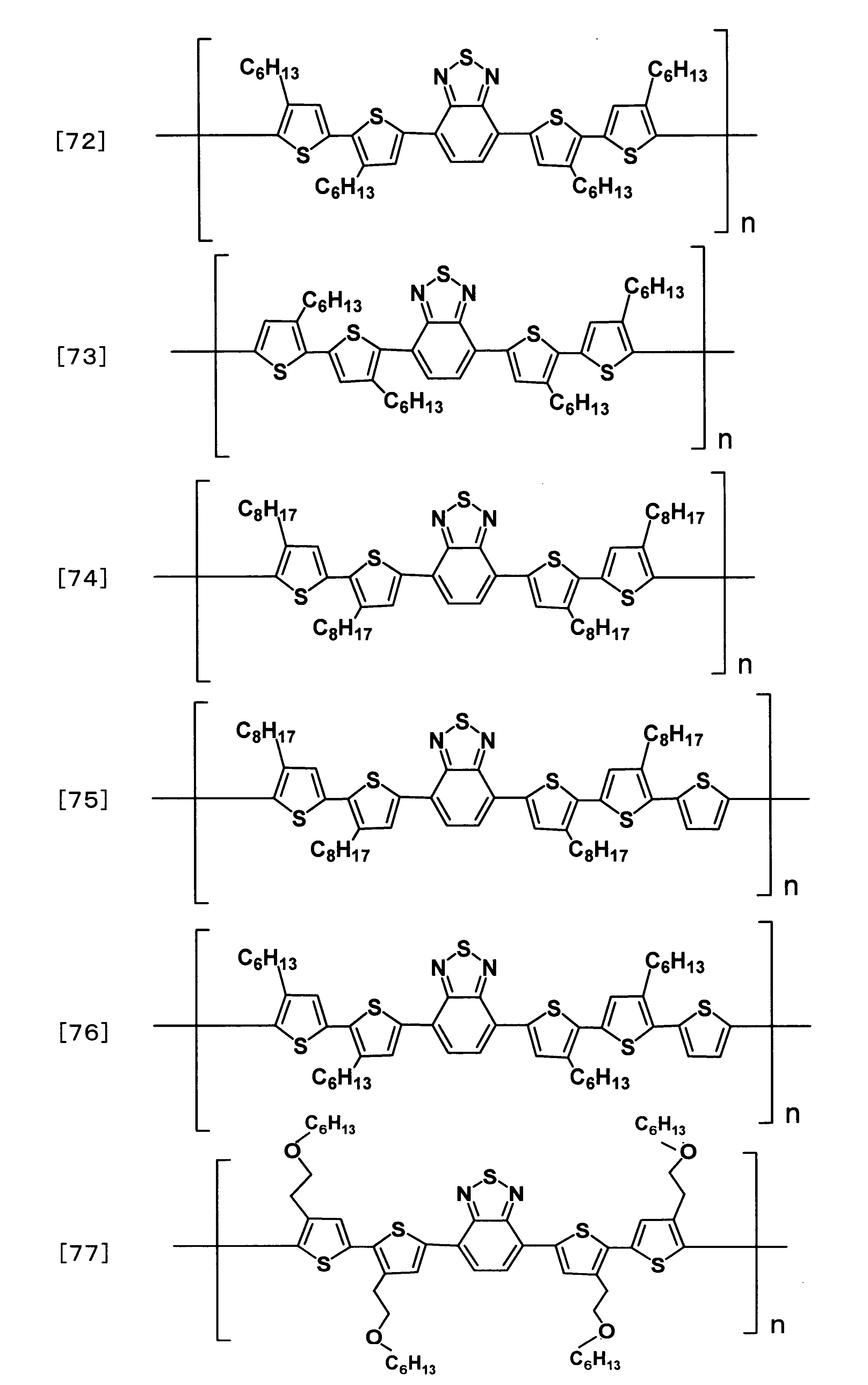

共役系重合体は、公知の方法により合成することができる。例えば、チオフェン同士を連結する方法としては、ハロゲン化チオフェンとチオフェンボロン酸またはチオフェンボロン酸エステルとを、パラジウム触媒下でカップリングする方法、ハロゲン化チオフェンとチオフェングリニヤール試薬とを、ニッケルまたはパラジウム触媒下でカップリングする方法が挙げられる。また、他のユニットとチオフェンユニットを連結する場合も、ハロゲン化した他のユニットとチオフェンユニットとを、同様の方法でカップリングすることができる。また、そのようにして得られたモノマーの末端に重合性官能基を導入し、パラジウム触媒やニッケル触媒下で重合を進行させることで、共役系重合体を得ることができる。
The conjugated polymer can be synthesized by a known method. For example, as a method of connecting thiophenes, a method of coupling a halogenated thiophene and a thiophene boronic acid or a thiophene boronic acid ester under a palladium catalyst, a halogenated thiophene and a thiophene Grignard reagent under a nickel or palladium catalyst And coupling methods. Moreover, also when connecting another unit and a thiophene unit, the halogenated other unit and a thiophene unit can be coupled by the same method. Also, a conjugated polymer can be obtained by introducing a polymerizable functional group at the terminal of the monomer thus obtained and advancing the polymerization under a palladium catalyst or a nickel catalyst.
共役系重合体は、合成過程で使用した原料や副生成物などの不純物を除去したものを用いることが好ましい。不純物を除去する方法としては、例えば、シリカゲルカラムグラフィー法、ソクスレー抽出法、ろ過法、イオン交換法、キレート法などを用いることができる。これらの方法を2種以上組み合わせてもよい。
As the conjugated polymer, it is preferable to use one from which impurities such as raw materials and by-products used in the synthesis process have been removed. As a method of removing the impurities, for example, silica gel column chromatography method, Soxhlet extraction method, filtration method, ion exchange method, chelate method and the like can be used. Two or more of these methods may be combined.
(半導体層)
半導体層は、ナノカーボンを含有する。このとき、ナノカーボンはフラーレン、CNT、グラフェンが好ましく、CNTがより好ましい。さらにCNTは、共役系重合体を付着せしめてCNT複合体として用いることが好ましい。半導体層は電気特性を阻害しない範囲であれば、さらに有機半導体や絶縁材料を含んでもよい。 (Semiconductor layer)
The semiconductor layer contains nanocarbon. At this time, the nanocarbon is preferably fullerene, CNT or graphene, more preferably CNT. Furthermore, it is preferable to attach a conjugated polymer and use CNT as a CNT composite. The semiconductor layer may further contain an organic semiconductor or an insulating material as long as the electric characteristics are not impaired.
半導体層の膜厚は、1nm以上100nm以下が好ましい。この範囲内にあることで、均一な薄膜形成が容易になる。半導体層の膜厚は、より好ましくは1nm以上50nm以下であり、さらに好ましくは1nm以上20nm以下である。膜厚は、原子間力顕微鏡やエリプソメトリ法などにより測定できる。
The thickness of the semiconductor layer is preferably 1 nm or more and 100 nm or less. Within this range, uniform thin film formation is facilitated. The thickness of the semiconductor layer is more preferably 1 nm or more and 50 nm or less, and still more preferably 1 nm or more and 20 nm or less. The film thickness can be measured by an atomic force microscope, ellipsometry or the like.
半導体層の形成方法としては、抵抗加熱蒸着、電子線ビーム、スパッタリング、CVDなど、乾式の方法を用いることも可能であるが、製造コストや大面積への適合の観点から、塗布法を用いることが好ましい。具体的には、スピンコート法、ブレードコート法、スリットダイコート法、スクリーン印刷法、バーコーター法、鋳型法、印刷転写法、浸漬引き上げ法、インクジェット法などを好ましく用いることができる。これらの中から、塗膜厚み制御や配向制御など、得ようとする塗膜特性に応じて塗布方法を選択することが好ましい。また、形成した塗膜に対して、大気下、減圧下または窒素やアルゴン等の不活性ガス雰囲気下で、アニーリング処理を行ってもよい。
As a method of forming the semiconductor layer, it is possible to use a dry method such as resistance heating evaporation, electron beam, sputtering, or CVD, but from the viewpoint of manufacturing cost and compatibility with a large area, use a coating method. Is preferred. Specifically, a spin coating method, a blade coating method, a slit die coating method, a screen printing method, a bar coater method, a mold method, a printing transfer method, an immersion pulling method, an inkjet method and the like can be preferably used. Among these, it is preferable to select the coating method according to the coating film characteristics to be obtained, such as coating film thickness control and orientation control. In addition, the formed coating may be subjected to an annealing treatment under the atmosphere, under reduced pressure, or under an inert gas atmosphere such as nitrogen or argon.
(第2絶縁層)
第2絶縁層は、半導体層に対してゲート絶縁層が形成された側の反対側に形成される。半導体層に対してゲート絶縁層が形成された側の反対側とは、例えば、半導体層の下側にゲート絶縁層を有する場合は、半導体層の上側を指す。第2絶縁層を形成することにより、半導体層を保護することができる。 (Second insulating layer)
The second insulating layer is formed on the semiconductor layer opposite to the side on which the gate insulating layer is formed. The side opposite to the side on which the gate insulating layer is formed with respect to the semiconductor layer refers to, for example, the upper side of the semiconductor layer when the gate insulating layer is provided below the semiconductor layer. By forming the second insulating layer, the semiconductor layer can be protected.
第2絶縁層は、一般式(1)で表される構造を少なくとも側鎖の一部に有するポリマーを含有する。該ポリマー中のアミノ基により、通常はp型半導体特性を示すCNT-FETを、n型半導体特性を示す半導体素子へ転換できる。さらに、アミノ基がポリマーの側鎖として固定されていることにより、n型TFT特性の安定性が向上すると推定される。
The second insulating layer contains a polymer having a structure represented by the general formula (1) in at least a part of a side chain. The amino group in the polymer can convert a CNT-FET, which usually exhibits p-type semiconductor characteristics, into a semiconductor element which exhibits n-type semiconductor characteristics. Furthermore, it is presumed that the stability of the n-type TFT characteristics is improved by fixing the amino group as the side chain of the polymer.

一般式(1)で表される構造を少なくとも側鎖の一部に有するポリマーの主鎖骨格としては、例えば、ポリオレフィン、ポリエステル、ポリアミド、ポリイミド、ポリウレタンおよびシロキサンなどが挙げられる。
As a main chain skeleton of the polymer which has a structure represented by General formula (1) in at least a part of side chain, polyolefin, polyester, polyamide, polyimide, polyurethane, siloxane, etc. are mentioned, for example.
一般式(1)中、R1およびR2は、それぞれ独立して、水素原子、炭素原子、窒素原子、酸素原子、ケイ素原子、リン原子および硫黄原子から選ばれる一種類以上の原子により構成される基を示す。R3およびR4は、それぞれ独立して、水素原子または下記一般式(2)で表される基を示す。
In the general formula (1), R 1 and R 2 are each independently composed of one or more atoms selected from hydrogen atom, carbon atom, nitrogen atom, oxygen atom, silicon atom, phosphorus atom and sulfur atom Group is shown. R 3 and R 4 each independently represent a hydrogen atom or a group represented by the following general formula (2).

一般式(2)中、R5~R7は、それぞれ独立して、水素原子、炭素原子、窒素原子、酸素原子、ケイ素原子、リン原子および硫黄原子から選ばれる一種類以上の原子により構成される基を示す。
In the general formula (2), R 5 to R 7 are each independently composed of one or more atoms selected from hydrogen atom, carbon atom, nitrogen atom, oxygen atom, silicon atom, phosphorus atom and sulfur atom Group is shown.
R1~R7としては、例えば、アルキル基、アルコキシ基、シクロアルキル基、アリール基、ヘテロアリール基、もしくはこれらの組み合わせからなる構造またはこれらとアミド基、エステル基、エーテル基、ウレア基、イミド基からなる群より選ばれる1種以上との組み合わせからなる構造などが挙げられるが、これに限られない。
As R 1 to R 7 , for example, a structure comprising an alkyl group, an alkoxy group, a cycloalkyl group, an aryl group, a heteroaryl group, or a combination thereof, or an amide group with these, an ester group, an ether group, a urea group, an imide Although the structure etc. which consist of a combination with 1 or more types selected from the group which consists of groups are mentioned, it is not restricted to this.
アリーレン基、ヘテロアリーレン基、アルキル基、アルコキシ基、シクロアルキル基、アリール基およびヘテロアリール基については、上記(カーボンナノチューブ複合体)の項で説明したとおりである。
The arylene group, the heteroarylene group, the alkyl group, the alkoxy group, the cycloalkyl group, the aryl group and the heteroaryl group are as described above in the section (Carbon nanotube composite).
一般式(1)中のアミノ基とは、窒素原子に結合する原子が水素原子または炭素原子である基である。ただし、その炭素原子にさらに結合する原子は、いずれも単結合により当該炭素原子と結合する。このようなアミノ基の具体例としては、例えば、メチルアミノ基、ジメチルアミノ基、ジシクロヘキシルアミノ基などが挙げられるが、これに限られない。また、アミノ基は、R1~R7にさらに含まれていても含まれていなくてもよい。
The amino group in the general formula (1) is a group in which the atom bonded to the nitrogen atom is a hydrogen atom or a carbon atom. However, any atom further bonded to the carbon atom is bonded to the carbon atom via a single bond. Specific examples of such an amino group include, for example, a methylamino group, a dimethylamino group, and a dicyclohexylamino group, but not limited thereto. In addition, the amino group may or may not be further contained in R 1 to R 7 .
一般式(1)で表される構造を少なくとも側鎖の一部に有するポリマーは、ポリマー中のアミノ基を構成する窒素原子の数とポリマーの総原子数との比(ポリマー中のアミノ基を構成する窒素原子の数/のポリマーの総原子数)が1/10000~1/10であることが好ましい。この範囲にあることで、アミノ基が有効に働き、n型半導体素子への転換を効果的に実現できると推定される。また、アミノ基が主鎖骨格やR1~R7にさらに含まれる場合、その窒素原子もアミノ基を構成する窒素原子の数に含める。
The polymer having the structure represented by the general formula (1) in at least a part of the side chain has a ratio of the number of nitrogen atoms constituting the amino group in the polymer to the total number of atoms of the polymer (amino group in the polymer It is preferable that the number of nitrogen atoms to constitute / the total number of atoms of the polymer) is 1/10000 to 1/10. By being in this range, it is presumed that the amino group works effectively and the conversion to the n-type semiconductor device can be effectively realized. When an amino group is further contained in the main chain skeleton or R 1 to R 7 , the nitrogen atom is also included in the number of nitrogen atoms constituting the amino group.
ポリマー中のアミノ基を構成する窒素原子の数とポリマーの総原子数との比は、XPSなどの元素分析により組成式およびアミノ基に該当する窒素原子量を決定することで算出できる。
The ratio of the number of nitrogen atoms constituting the amino group in the polymer to the total number of atoms of the polymer can be calculated by determining the composition formula and the nitrogen atom weight corresponding to the amino group by elemental analysis such as XPS.
入手容易性およびコストの観点から、一般式(1)で表される構造を少なくとも側鎖の一部に有するポリマーは、一般式(3)で表される単位構造を有するポリマーであることが好ましい。
From the viewpoint of availability and cost, it is preferable that the polymer having at least a part of the side chain a structure represented by General Formula (1) is a polymer having a unit structure represented by General Formula (3) .

一般式(3)中、R1~R4は上記の通りである。R8は、単結合、または、炭素原子、酸素原子、窒素原子、ケイ素原子、リン原子および硫黄原子から選ばれる一種類以上の原子により構成される二価の基を示す。R9は、水素原子、炭素原子、窒素原子、酸素原子、ケイ素原子、リン原子および硫黄原子から選ばれる一種類以上の原子により構成される基を示す。
In the general formula (3), R 1 to R 4 are as described above. R 8 represents a single bond or a divalent group constituted by one or more types of atoms selected from carbon atom, oxygen atom, nitrogen atom, silicon atom, phosphorus atom and sulfur atom. R 9 represents a group constituted by one or more types of atoms selected from hydrogen atom, carbon atom, nitrogen atom, oxygen atom, silicon atom, phosphorus atom and sulfur atom.
R8としては、例えば、アルキレン基、オキシアルキレン基、シクロアルキレン基、アリーレン基、ヘテロアリーレン基、もしくはこれらの組み合わせからなる構造またはこれらとアミド基、エステル基、エーテル基、ウレア基、イミド基からなる群より選ばれる1種以上との組み合わせからなる構造などが挙げられるが、これに限られない。
As R 8 , for example, a structure comprising an alkylene group, an oxyalkylene group, a cycloalkylene group, an arylene group, a heteroarylene group, or a combination thereof, or an amide group with these, an ester group, an ether group, a urea group or an imide group Although the structure etc. which consist of a combination with 1 or more types selected from is included, it is not restricted to this.
R9としては、例えば、アルキル基、アルコキシ基、シクロアルキル基、アリール基、ヘテロアリール基、もしくはこれらの組み合わせからなる構造またはこれらとアミド基、エステル基、エーテル基、ウレア基、イミド基からなる群より選ばれる1種以上との組み合わせからなる構造などが挙げられるが、これに限られない。
As R 9 , for example, a structure comprising an alkyl group, an alkoxy group, a cycloalkyl group, an aryl group, a heteroaryl group or a combination thereof or an amide group, an ester group, an ether group, a urea group or an imide group Although the structure etc. which consist of a combination with 1 or more types chosen from a group are mentioned, it is not restricted to this.
これらの基のうち、アルキレン基とは、例えば、メチレン基、エチレン基、n-プロピレン基、イソプロピレン基、n-ブチレン基、sec-ブチレン基、tert-ブチレン基などの2価の飽和脂肪族炭化水素基を示す。アルキレン基は、さらに置換基を有していても有していなくてもよい。また、アルキレン基の炭素数は特に限定されないが、入手の容易性やコストの点から、1以上20以下が好ましく、より好ましくは1以上8以下である。
Among these groups, an alkylene group is, for example, a divalent saturated aliphatic group such as methylene group, ethylene group, n-propylene group, isopropylene group, n-butylene group, sec-butylene group, tert-butylene group, etc. Indicates a hydrocarbon group. The alkylene group may or may not further have a substituent. The carbon number of the alkylene group is not particularly limited, but is preferably 1 or more and 20 or less, more preferably 1 or more and 8 or less from the viewpoint of availability and cost.
オキシアルキレン基とは、例えば、オキシエチレン基、オキシプロピレン基などのエーテル結合を介して脂肪族炭化水素基が結合した2価の官能基を示し、この脂肪族炭化水素基はさらに置換基を有していても有していなくてもよい。オキシアルコキシ基の炭素数は特に限定されないが、1以上20以下の範囲が好ましい。
The oxyalkylene group indicates, for example, a divalent functional group in which an aliphatic hydrocarbon group is bonded via an ether bond such as an oxyethylene group or an oxypropylene group, and the aliphatic hydrocarbon group further has a substituent. It may or may not have. The carbon number of the oxyalkoxy group is not particularly limited, but a range of 1 or more and 20 or less is preferable.
シクロアルキレン基とは、例えば、シクロプロピレン基、シクロブチレン基、シクロペンチレン基、シクロへキシレン基などの2価の飽和脂環式炭化水素基を示し、これは置換基を有していても有していなくてもよい。シクロアルキレン基の炭素数は特に限定されないが、2以上20以下の範囲が好ましい。
The cycloalkylene group is, for example, a divalent saturated alicyclic hydrocarbon group such as a cyclopropylene group, a cyclobutylene group, a cyclopentylene group, a cyclohexylene group or the like, which may have a substituent. You do not need to have it. The carbon number of the cycloalkylene group is not particularly limited, but a range of 2 or more and 20 or less is preferable.
一般式(3)で表される単位構造としては、例えば、2-(ジメチルアミノ)エチルアクリレート、2-(ジエチルアミノ)エチルアクリレート、2-(ジエチルアミノ)エチルアクリレート、2-(ジイソプロピルアミノ)エチルアクリレート、2-(ジメチルアミノ)イソプロピルアクリレートなどのアクリル系モノマーおよびこれらのアクリレートをメタクリレートに代えたものなどをモノマーとしたアクリル樹脂の繰返し単位構造などが挙げられる。上記繰返し単位構造は、単独あるいは2種以上でもよい。
As a unit structure represented by General formula (3), for example, 2- (dimethylamino) ethyl acrylate, 2- (diethylamino) ethyl acrylate, 2- (diethylamino) ethyl acrylate, 2- (diisopropylamino) ethyl acrylate, Examples thereof include acrylic monomers such as 2- (dimethylamino) isopropyl acrylate and a repeating unit structure of an acrylic resin using a monomer obtained by replacing such acrylate with methacrylate. The repeating unit structure may be used alone or in combination of two or more.
一般式(3)で表される単位構造を有するポリマーとしては、例えば、ポリアリルアミン、ポリ(ジメチルアリルアミン)などが挙げられる。
Examples of the polymer having a unit structure represented by the general formula (3) include polyallylamine and poly (dimethylallylamine).
上記一般式(1)で表される構造を少なくとも側鎖の一部に有するポリマーは、さらに一般式(4)で表される単位構造を有することがより好ましい。Yのような極性基の存在により、アミノ基が有効に働き、n型半導体素子への転換を効果的に実現できると推定される。
It is more preferable that the polymer which has a structure represented by the said General formula (1) in a part of side chain at least has a unit structure further represented by General formula (4). Due to the presence of a polar group such as Y, it is presumed that the amino group works effectively and the conversion to an n-type semiconductor device can be effectively realized.

一般式(4)中、Yは、アミド基、エステル基、ウレア基、カルボニル基、イミド基、ウレイド基、チオアミド基、チオエステル基、チオウレア基、チオカルボニル基、チオイミド基およびチオウレイド基からなる群から選ばれる基を示す。R10は、水素原子、炭素原子、酸素原子、ケイ素原子、リン原子および硫黄原子から選ばれる一種類以上の原子により構成される基を示す。R11は、単結合、または、水素原子、炭素原子、酸素原子、ケイ素原子、リン原子および硫黄原子から選ばれる一種類以上の原子により構成される二価の基を示す。R12は、炭素原子、窒素原子、酸素原子、ケイ素原子、リン原子および硫黄原子から選ばれる一種類以上の原子により構成される基を示す。
In the general formula (4), Y represents an amide group, an ester group, a urea group, a carbonyl group, an imide group, a ureido group, a thioamide group, a thioester group, a thiourea group, a thiocarbonyl group, a thioimide group and a thioureido group Indicates the selected group. R 10 represents a group constituted by one or more kinds of atoms selected from a hydrogen atom, a carbon atom, an oxygen atom, a silicon atom, a phosphorus atom and a sulfur atom. R 11 represents a single bond or a divalent group constituted by one or more kinds of atoms selected from a hydrogen atom, a carbon atom, an oxygen atom, a silicon atom, a phosphorus atom and a sulfur atom. R 12 represents a group constituted by one or more types of atoms selected from carbon atom, nitrogen atom, oxygen atom, silicon atom, phosphorus atom and sulfur atom.
R10としては、例えば、アルキル基、アルコキシ基、シクロアルキル基、アリール基、ヘテロアリール基、もしくはこれらの組み合わせからなる構造またはこれらとエステル基およびエーテル基からなる群より選ばれる1種以上との組み合わせからなる構造などが挙げられるが、これに限られない。
R 10 represents, for example, a structure consisting of an alkyl group, an alkoxy group, a cycloalkyl group, an aryl group, a heteroaryl group, or a combination thereof or one or more selected from the group consisting of an ester group and an ether group Although the structure etc. which consist of a combination etc. are mentioned, it is not restricted to this.
R11としては、例えば、アルキレン基、オキシアルキレン基、シクロアルキレン基、アリーレン基、ヘテロアリーレン基、もしくはこれらの組み合わせからなる構造またはこれらとエステル基およびエーテル基からなる群より選ばれる1種以上との組み合わせからなる構造などが挙げられるが、これに限られない。
R 11 is, for example, one or more selected from the group consisting of an alkylene group, an oxyalkylene group, a cycloalkylene group, an arylene group, a heteroarylene group, or a combination thereof or an ester group and an ether group Although the structure etc. which consist of combinations of is mentioned, it is not restricted to this.
R12としては、例えば、アルキル基、アルコキシ基、シクロアルキル基、アリール基、ヘテロアリール基、もしくはこれらの組み合わせからなる構造またはこれらとエステル基およびエーテル基からなる群より選ばれる1種以上との組み合わせからなる構造などが挙げられるが、これに限られない。
As R 12 , for example, a structure consisting of an alkyl group, an alkoxy group, a cycloalkyl group, an aryl group, a heteroaryl group, or a combination thereof or one or more selected from the group consisting of an ester group and an ether group Although the structure etc. which consist of a combination etc. are mentioned, it is not restricted to this.
一般式(4)で表される単位構造としては、例えば、メチルアクリレート、2-エチルヘキシルアクリレート、エチルアクリレート、n-ブチルアクリレート、i-ブチルアクリレート、i-プロパンアクリレート、N-メトキシメチルアクリルアミド、N-エトキシメチルアクリルアミド、N-n-ブトキシメチルアクリルアミド、N-イソブトキシメチルアクリルアミド、ブトキシトリエチレングリコールアクリレート、ジシクロペンタニルアクリレート、2-ヒドロキシエチルアクリレート、イソボルニルアクリレート、2-ヒドロキシプロピルアクリレート、イソデシルアクリレート、イソオクチルアクリレート、ラウリルアクリレート、2-メトキシエチルアクリレート、メトキシエチレングリコールアクリレート、メトキシジエチレングリコールアクリレート、オクタフロロペンチルアクリレート、フェノキシエチルアクリレート、ステアリルアクリレート、トリフロロエチルアクリレート、フェニルアクリレート、フェノキシエチルアクリレート、1-ナフチルアクリレート、2-ナフチルアクリレート、チオフェノールアクリレート、などのアクリル系モノマーおよびこれらのアクリレートをメタクリレートに代えたものなどをモノマーとしたアクリル樹脂の繰返し単位構造;ポリビニルピロリドンの繰返し単位構造;上記エステル基をウレア基、カルボニル基、イミド基、ウレイド基、チオアミド基、チオエステル基、チオウレア基、チオカルボニル基、チオイミド基、チオウレイド基に置換した繰返し単位構造、などが挙げられる。上記繰返し単位構造は、単独あるいは2種以上でもよい。また、上記繰返し単位構造中に、Yは1つでもよいし複数含まれていてもよい。
Examples of the unit structure represented by the general formula (4) include methyl acrylate, 2-ethylhexyl acrylate, ethyl acrylate, n-butyl acrylate, i-butyl acrylate, i-propane acrylate, N-methoxymethyl acrylamide, N- Ethoxymethyl acrylamide, Nn-butoxymethyl acrylamide, N-isobutoxy methyl acrylamide, butoxy triethylene glycol acrylate, dicyclopentanyl acrylate, 2-hydroxyethyl acrylate, isobornyl acrylate, 2-hydroxypropyl acrylate, isodecyl Acrylate, isooctyl acrylate, lauryl acrylate, 2-methoxyethyl acrylate, methoxy ethylene glycol acrylate, methoxy di Acrylic monomers such as thylene glycol acrylate, octafluoropentyl acrylate, phenoxyethyl acrylate, stearyl acrylate, trifluoroethyl acrylate, phenyl acrylate, phenoxyethyl acrylate, 1-naphthyl acrylate, 2-naphthyl acrylate, thiophenol acrylate, and the like Repeating unit structure of an acrylic resin using, as a monomer, one obtained by replacing acrylate with methacrylate; repeating unit structure of polyvinylpyrrolidone; the above-mentioned ester group is urea group, carbonyl group, imide group, ureido group, thioamide group, thioester group, thiourea group , A thiocarbonyl group, a thioimide group, a repeating unit structure substituted with a thioureido group, and the like. The repeating unit structure may be used alone or in combination of two or more. In addition, one or more Y may be contained in the repeating unit structure.
一般式(3)および(4)で表される単位構造を有するポリマーは、一般式(4)で表される単位構造と一般式(3)で表される単位構造との比率[一般式(4)で表される単位構造のモル数/一般式(3)で表される単位構造のモル数]が90/10~10/90であることが好ましい。この範囲にあることで、アミノ基が有効に働き、n型半導体素子への転換を効果的に実現できると推定される。係る比率はより好ましくは、90/10~30/70、さらに好ましくは、90/10~40/60である。一般式(4)で表される単位構造と一般式(3)で表される単位構造との比率は、XPSによりアミノ基やYの比率を評価することで算出できる。
The polymer having a unit structure represented by the general formulas (3) and (4) has a ratio of the unit structure represented by the general formula (4) to the unit structure represented by the general formula (3) It is preferable that the number of moles of the unit structure represented by 4) / the number of moles of the unit structure represented by the general formula (3) is 90/10 to 10/90. By being in this range, it is presumed that the amino group works effectively and the conversion to the n-type semiconductor device can be effectively realized. The ratio is more preferably 90/10 to 30/70, still more preferably 90/10 to 40/60. The ratio of the unit structure represented by the general formula (4) to the unit structure represented by the general formula (3) can be calculated by evaluating the ratio of the amino group or Y by XPS.
第2絶縁層の膜厚は、500nm以上であることが好ましく、1.0μm以上であることがより好ましく、3.0μm以上であることがさらに好ましく、10μm以上であることが特に好ましい。この範囲の膜厚にすることにより、より高いn型半導体特性を示す半導体素子へと転換でき、また、n型TFT特性の安定性が向上する。また、上限としては、特に限定されるものではないが、500μm以下であることが好ましい。
The thickness of the second insulating layer is preferably 500 nm or more, more preferably 1.0 μm or more, still more preferably 3.0 μm or more, and particularly preferably 10 μm or more. By setting the film thickness within this range, conversion to a semiconductor element exhibiting higher n-type semiconductor characteristics can be achieved, and the stability of n-type TFT characteristics is improved. The upper limit is not particularly limited, but is preferably 500 μm or less.
第2絶縁層の膜厚は、第2絶縁層の断面を走査型電子顕微鏡により測定し、得られた像のうち、半導体層上に位置する第2絶縁層部分の中から無作為に選択した10箇所の膜厚を算出し、その算術平均の値とする。
The film thickness of the second insulating layer was randomly selected from among the portions of the second insulating layer located on the semiconductor layer in the image obtained by measuring the cross section of the second insulating layer with a scanning electron microscope The film thickness at 10 locations is calculated and taken as the value of the arithmetic mean.
また、第2絶縁層は、窒素原子およびリン原子から選ばれる1種以上の原子を有する電子供与性化合物をさらに含有することが好ましい。電子供与性とは、ある化合物が別の化合物へ電子を供与する能力のことである。電子供与性化合物は、電子供与する能力を有する化合物である。第2絶縁層にそのような電子供与性化合物が含まれることにより、より高いn型半導体特性を有する半導体素子へ転換できる。
The second insulating layer preferably further contains an electron donating compound having one or more atoms selected from a nitrogen atom and a phosphorus atom. Electron donating ability refers to the ability of one compound to donate an electron to another compound. The electron donating compound is a compound having an electron donating ability. By including such an electron donating compound in the second insulating layer, it can be converted to a semiconductor element having higher n-type semiconductor characteristics.
電子供与性化合物としては、例えば、アミン系化合物、イミン系化合物、アニリン系化合物、ニトリル系化合物、アルキルホスフィン系化合物などを挙げることができる。
As an electron donor, an amine compound, an imine type compound, an aniline type compound, a nitrile type compound, an alkyl phosphine type compound etc. can be mentioned, for example.
アミン系化合物としては、メチルアミン、ジメチルアミン、トリメチルアミン、エチルアミン、ジエチルアミン、トリエチルアミン、ジイソプロピルエチルアミン、シクロヘキシルアミン、メチルシクロヘキシルアミン、ジメチルシクロヘキシルアミン、ジシクロヘキシルアミン、ジシクロヘキシルメチルアミン、トリシクロヘキシルアミン、シクロオクチルアミン、シクロデシルアミン、シクロドデシルアミン、1-アザビシクロ[2.2.2]オクタン(キヌクリジン)、1,8-ジアザビシクロ[5.4.0]ウンデカ-7-エン(DBU)、1,5-ジアザビシクロ[4.3.0]ノナ-5-エン(DBN)、1,5,7-トリアザビシクロ[4.4.0]デカ-5-エン(TBD)、7-メチル-1,5,7-トリアザビシクロ[4.4.0]デカ-5-エン(MTBD)、ポリ(メラミン-co-ホルムアルデヒド)、テトラメチルエチレンジアミン、ジフェニルアミン、トリフェニルアミン、フェニルアラニン、N,N-ジメチルー4-アミノピリジンなどが挙げられる。
Examples of amine compounds include methylamine, dimethylamine, trimethylamine, ethylamine, diethylamine, triethylamine, diisopropylethylamine, cyclohexylamine, methylcyclohexylamine, dimethylcyclohexylamine, dicyclohexylamine, dicyclohexylmethylamine, tricyclohexylamine, cyclooctylamine and cyclooctylamine. Decylamine, cyclododecylamine, 1-azabicyclo [2.2.2] octane (quinuclidine), 1,8-diazabicyclo [5.4.0] undec-7-ene (DBU), 1,5-diazabicyclo [4 .3.0] Non-5-ene (DBN), 1,5,7-triazabicyclo [4.4.0] dec-5-ene (TBD), 7-methyl-1,5,7-tria Xabicyclo 4.4.0] dec-5-ene (MTBD), poly (melamine -co- formaldehyde), tetramethylethylenediamine, diphenylamine, triphenylamine, phenylalanine, N, etc. N- dimethyl-4-aminopyridine.
イミン系化合物としては、エチレンイミン、N-メチルヘキサン-1-イミン、N-メチル-1-ブチル-1-ヘキサンイミン、プロパン-2-イミン、メタンジイミン、N-メチルエタンイミン、エタン-1,2-ジイミンなどが挙げられる。
Examples of imine compounds include ethyleneimine, N-methylhexane-1-imine, N-methyl-1-butyl-1-hexaneimine, propane-2-imine, methanediimine, N-methylethaneimine, ethane-1,2 -Diimine etc. are mentioned.
アニリン系化合物としては、アニリン、トルイジンなどが挙げられる。
Aniline, toluidine etc. are mentioned as an aniline type compound.
ニトリル系化合物としては、アセトニトリル、アクリロニトリルなどが挙げられる。その他の化合物としてはアラントイン、2-イミダゾリジノン、1,3-ジメチル-2-イミダゾリジノン、ジシアンジアミジン、シトルリン、ピペリジン、イミダゾール、ピリミジン、ジュロリジンなどが挙げられる。
Examples of nitrile compounds include acetonitrile and acrylonitrile. Other compounds include allantoin, 2-imidazolidinone, 1,3-dimethyl-2-imidazolidinone, dicyandiamidine, citrulline, piperidine, imidazole, pyrimidine, julolidine and the like.
アルキルホスフィン系化合物としては、トリブチルホスフィン、トリ-tert-ブチルホスフィン、トリフェニルホスフィンなどが挙げられる。
Examples of alkyl phosphine compounds include tributyl phosphine, tri-tert-butyl phosphine, triphenyl phosphine and the like.
これらの中でも、より高いn型半導体特性の発現の観点から、電子供与性化合物は窒素原子を有する化合物であることが好ましく、特には窒素原子を含む環構造を含有する化合物であることがより好ましい。窒素原子を含む環構造を含有する化合物としては、ポリビニルピロリドン、N-メチルピロリドン、ポリビニルポリピロリドン、β-ラクタム、γ-ラクタム、δ-ラクタム、ε-カプロラクタム、ポリイミド、フタルイミド、マレイミド、アロキサン、スクシンイミド、ウラシル、チミン、2-イミダゾリジノン、1,3-ジメチル-2-イミダゾリジノン、キヌクリジン、DBU、DBN、TBD、MTBD、ピペリジン、イミダゾール、ピリミジン、ジュロリジンなどが挙げられる。
Among these, from the viewpoint of expression of higher n-type semiconductor characteristics, the electron donating compound is preferably a compound having a nitrogen atom, and more preferably a compound having a ring structure containing a nitrogen atom. . Examples of the compound having a ring structure containing a nitrogen atom include polyvinyl pyrrolidone, N-methyl pyrrolidone, polyvinyl polypyrrolidone, β-lactam, γ-lactam, δ-lactam, ε-caprolactam, polyimide, phthalimide, maleimide, maleimide, alloxane, succinimide Uracil, thymine, 2-imidazolidinone, 1,3-dimethyl-2-imidazolidinone, quinuclidine, DBU, DBN, TBD, MTBD, piperidine, imidazole, pyrimidine, julolidine and the like.
また、電子供与性化合物は、アミジン化合物およびグアニジン化合物から選ばれるいずれか1種類以上の化合物であることが、特に好ましい。アミジン化合物としては、DBU、DBNなどが挙げられる。グアニジン化合物としては、TBD、MTBDなどが挙げられる。これらの化合物は、電子供与性が特に高く、そのため、CNTを用いたFETのn型半導体素子としての性能がさらに向上するため、好ましい。
Further, it is particularly preferable that the electron donor compound is any one or more compounds selected from an amidine compound and a guanidine compound. Examples of amidine compounds include DBU and DBN. Examples of guanidine compounds include TBD and MTBD. These compounds are preferable because they have particularly high electron donating properties, and thus the performance of the CNT using FET as an n-type semiconductor device is further improved.
第2絶縁層は単層でも複数層でもよく、また、1つの層を複数の絶縁性材料から形成してもよいし、複数の絶縁性材料を積層して形成しても構わない。
The second insulating layer may be a single layer or a plurality of layers, one layer may be formed of a plurality of insulating materials, or a plurality of insulating materials may be stacked.
第2絶縁層の形成方法としては、特に限定されず、抵抗加熱蒸着、電子線ビーム、スパッタリング、CVDなど乾式の方法を用いることも可能であるが、製造コストや大面積への適合の観点から塗布法を用いることが好ましい。塗布法では、第2絶縁層が含有するポリマーおよび溶剤を含有する組成物を塗布および乾燥する工程を少なくとも含む。
The method of forming the second insulating layer is not particularly limited, and dry methods such as resistance heating evaporation, electron beam, sputtering, and CVD may be used, but from the viewpoint of manufacturing cost and adaptation to a large area. It is preferable to use a coating method. The application method at least includes the steps of applying and drying a composition containing a polymer and a solvent contained in the second insulating layer.
塗布方法としては、具体的には、スピンコート法、ブレードコート法、スリットダイコート法、スクリーン印刷法、バーコーター法、鋳型法、印刷転写法、浸漬引き上げ法、インクジェット法、ドロップキャスト法などを好ましく用いることができる。これらの中から、塗膜厚み制御や配向制御など、得ようとする塗膜特性に応じて塗布方法を選択することが好ましい。
Specifically, spin coating method, blade coating method, slit die coating method, screen printing method, bar coater method, mold method, printing transfer method, immersion pulling method, ink jet method, drop casting method etc. are preferable as the coating method. It can be used. Among these, it is preferable to select the coating method according to the coating film characteristics to be obtained, such as coating film thickness control and orientation control.
塗布法を用いて第2絶縁層を形成するに際して、第2絶縁層が含有するポリマーを溶解させる溶媒としては、特に制限されないが、有機溶媒が好ましい。溶媒の具体例としては、例えば、エチレングリゴールモノメチルエーテル、エチレングリコールモノエチルエーテル、プロピレングリコールモノメチルエーテル、プロピレングリコールモノエチルエーテル、プロピレングリコールモノn-ブチルエーテル、プロピレングリコールモノt-ブチルエーテル、エチレングリコールジメチルエーテル、エチレングリコールジエチルエーテル、エチレングリコールジブチルエーテル、ジエチレングリコールエチルメチルエーテル等のエーテル類;エチレングリコールモノエチルエーテルアセテート、プロピレングリコールモノメチルエーテルアセテート、プロピルアセテート、ブチルアセテート、イソブチルアセテート、3-メトキシブチルアセテート、3-メチル-3-メトキシブチルアセテート、乳酸メチル、乳酸エチル、乳酸ブチル等のエステル類;アセトン、メチルエチルケトン、メチルプロピルケトン、メチルブチルケトン、メチルイソブチルケトン、シクロペンタノン、2-ヘプタノン等のケトン類;ブチルアルコール、イソブチルアルコール、ペンタノール、4-メチル-2-ペンタノール、3-メチル-2-ブタノール、3-メチル-3-メトキシブタノール、ジアセトンアルコール等のアルコール類;トルエン、キシレン等の芳香族炭化水素類;ヘキサン、デカヒドロナフタレン等の炭化水素類が挙げられる。
The solvent for dissolving the polymer contained in the second insulating layer when forming the second insulating layer using a coating method is not particularly limited, but an organic solvent is preferable. Specific examples of the solvent include, for example, ethylene glycol monomethyl ether, ethylene glycol monoethyl ether, propylene glycol monomethyl ether, propylene glycol monoethyl ether, propylene glycol mono n-butyl ether, propylene glycol mono t-butyl ether, ethylene glycol dimethyl ether, Ethers such as ethylene glycol diethyl ether, ethylene glycol dibutyl ether and diethylene glycol ethyl methyl ether; ethylene glycol monoethyl ether acetate, propylene glycol monomethyl ether acetate, propyl acetate, butyl acetate, isobutyl acetate, 3-methoxybutyl acetate, 3-methyl -3-Methoxybutyl acetate Esters such as methyl lactate, ethyl lactate and butyl lactate; acetones such as methyl ethyl ketone, methyl propyl ketone, methyl butyl ketone, methyl isobutyl ketone, methyl isobutyl ketone, cyclopentanone and 2-heptanone; butyl alcohol, isobutyl alcohol, pentanol, Alcohols such as 4-methyl-2-pentanol, 3-methyl-2-butanol, 3-methyl-3-methoxybutanol, diacetone alcohol; Aromatic hydrocarbons such as toluene and xylene; Hexane, decahydronaphthalene And the like.
溶媒として、これらを2種以上用いてもよい。中でも、1気圧における沸点が110~200℃の溶媒を含有することが好ましい。溶媒の沸点が110℃以上であれば、溶液塗布時に溶剤の揮発が抑制されて、塗布性が良好となる。溶媒の沸点が200℃以下であれば、絶縁膜中に残存する溶剤が少なくなり、より良好な耐熱性や耐薬品性を有する第2絶縁層が得られる。
Two or more of these may be used as the solvent. Among them, it is preferable to contain a solvent having a boiling point of 110 to 200 ° C. at 1 atm. When the boiling point of the solvent is 110 ° C. or more, volatilization of the solvent is suppressed at the time of solution application, and the coatability becomes good. When the boiling point of the solvent is 200 ° C. or less, the amount of the solvent remaining in the insulating film is reduced, and the second insulating layer having better heat resistance and chemical resistance can be obtained.
また、形成した塗膜に対して、大気下、減圧下または窒素やアルゴン等の不活性ガス雰囲気下でアニーリング処理や熱風乾燥を行ってもよい。具体的には例えば、アニーリングの条件としては、50~150℃、3~30分、窒素雰囲気下が挙げられる。このような乾燥工程により、塗膜の乾燥が不十分である場合に、しっかり乾燥させることができる。
In addition, the formed coating may be subjected to annealing treatment or hot-air drying in the atmosphere, under reduced pressure, or in an inert gas atmosphere such as nitrogen or argon. Specifically, for example, the annealing conditions include 50 to 150 ° C., 3 to 30 minutes, and under a nitrogen atmosphere. Such a drying step allows firm drying if the coating is not sufficiently dried.
(バリア層)
本発明の実施の形態に係るn型半導体素子は、第2絶縁層上に、水蒸気透過度が20g/(m2・24h)以下である層(バリア層)を有することが好ましい。バリア層の水蒸気透過度は、より好ましくは10g/(m2・24h)以下であり、さらに好ましくは1g/(m2・24h)以下である。この範囲にあることで、大気中の水分の影響を受けにくく、安定したn型半導体特性を実現できる。 (Barrier layer)
The n-type semiconductor device according to the embodiment of the present invention preferably includes a layer (barrier layer) having a water vapor transmission rate of 20 g / (m 2 · 24 h) or less on the second insulating layer. The water vapor transmission rate of the barrier layer is more preferably 10 g / (m 2 · 24 h) or less, still more preferably 1 g / (m 2 · 24 h) or less. By being in this range, stable n-type semiconductor characteristics can be realized without being affected by moisture in the air.
図3は、本発明の実施の形態に係る半導体素子の第三の例を示す模式断面図である。絶縁性の基材1の上に形成されるゲート電極2と、それを覆うゲート絶縁層3と、その上に設けられるソース電極5およびドレイン電極6と、それらの電極の間に設けられる半導体層4と、半導体層を覆う第2絶縁層8と、第2絶縁層を覆うバリア層9と、を有する。半導体層4は、ナノカーボン7を含む。
FIG. 3 is a schematic cross-sectional view showing a third example of the semiconductor device according to the embodiment of the present invention. A gate electrode 2 formed on an insulating base material 1, a gate insulating layer 3 covering it, a source electrode 5 and a drain electrode 6 provided thereon, and a semiconductor layer provided between the electrodes 4, a second insulating layer 8 covering the semiconductor layer, and a barrier layer 9 covering the second insulating layer. The semiconductor layer 4 contains nanocarbon 7.
図4は、本発明の実施の形態に係る半導体素子の第四の例を示す模式断面図である。絶縁性の基材1の上に形成されるゲート電極2と、それを覆うゲート絶縁層3と、その上に設けられる半導体層4と、その上に形成されるソース電極5およびドレイン電極6と、それらの上に設けられる第2絶縁層8と、第2絶縁層を覆うバリア層9と、を有する。半導体層4は、ナノカーボン7を含む。
FIG. 4 is a schematic cross-sectional view showing a fourth example of the semiconductor device according to the embodiment of the present invention. A gate electrode 2 formed on an insulating substrate 1, a gate insulating layer 3 covering it, a semiconductor layer 4 provided thereon, and a source electrode 5 and a drain electrode 6 formed thereon , And a second insulating layer 8 provided thereon, and a barrier layer 9 covering the second insulating layer. The semiconductor layer 4 contains nanocarbon 7.
n型半導体素子の性能安定性の観点から、バリア層は、フッ素系樹脂、塩素系樹脂、二トリル樹脂、ポリエステル、ポリオレフィンから選ばれるいずれか1種類以上を含有することが好ましい。これらのポリマーは水蒸気透過性が低いことに加え、塗布法によりバリア層を形成するプロセスにおいて、穏和なアニーリング条件での乾燥による製膜が可能であり、アニーリングによるn型半導体素子の特性劣化を抑制できるためである。
From the viewpoint of the performance stability of the n-type semiconductor device, the barrier layer preferably contains one or more selected from fluorine resins, chlorine resins, nitrile resins, polyesters, and polyolefins. In addition to the low water vapor permeability of these polymers, film formation by drying under mild annealing conditions is possible in the process of forming a barrier layer by a coating method, and the characteristic deterioration of n-type semiconductor devices due to annealing is suppressed. It is because it can.
フッ素系樹脂とは、フッ素原子を含有するポリマーであり、例えば、ポリフッ化ビニル、ポリフッ化ビニリデン、ポリテトラフルオロエチレン、ポリクロロトリフルオロエチレン、フッ化ビニリデンー三フッ化エチレンの共重合体などが挙げられる。
The fluorine-based resin is a polymer containing a fluorine atom, and examples thereof include polyvinyl fluoride, polyvinylidene fluoride, polytetrafluoroethylene, polychlorotrifluoroethylene, and copolymers of vinylidene fluoride and trifluorinated ethylene. Be
塩素系樹脂とは、塩素原子を含有するポリマーであり、例えば、ポリビニルクロリド、ポリ塩化ビニリデン、ビニルクロリド―ビニル酢酸共重合体などが挙げられる。
The chlorine-based resin is a polymer containing a chlorine atom, and examples thereof include polyvinyl chloride, polyvinylidene chloride, a vinyl chloride-vinyl acetate copolymer and the like.
二トリル樹脂は、ニトリル基を含有するポリマーであり、例えば、ポリアクリロニトリル、ポリアリルシアニドなどが挙げられる。
The nitrile resin is a polymer containing a nitrile group, and examples thereof include polyacrylonitrile, polyallyl cyanide and the like.
ポリエステルとしては、例えば、ポリエチレンテレフタレートなどが挙げられる。
As polyester, a polyethylene terephthalate etc. are mentioned, for example.
ポリオレフィンとしては、例えば、ポリエチレン、ポリプロピレン、ポリブタジエン、ポリスチレン、シクロオレフィンポリマーなどが挙げられる。
Examples of the polyolefin include polyethylene, polypropylene, polybutadiene, polystyrene, cycloolefin polymer and the like.
水蒸気透過の観点から、フッ素系樹脂、塩素系樹脂、ポリオレフィン樹脂がより好ましく、中でも、ポリテトラフルオロエチレン、ポリクロロトリフルオロエチレン、ポリ塩化ビニリデン、シクロオレフィンポリマーが好ましい。
From the viewpoint of water vapor permeation, fluorine resins, chlorine resins and polyolefin resins are more preferable. Among them, polytetrafluoroethylene, polychlorotrifluoroethylene, polyvinylidene chloride and cycloolefin polymers are preferable.
バリア層の膜厚は、1.0μm以上であることが好ましく、3.0μm以上であることがさらに好ましく、10μm以上であることが特に好ましい。この範囲の膜厚にすることにより、バリア層による水蒸気遮蔽性を高めることができる。また、上限としては、特に限定されるものではないが、500μm以下であることが好ましい。
The film thickness of the barrier layer is preferably 1.0 μm or more, more preferably 3.0 μm or more, and particularly preferably 10 μm or more. By setting the film thickness in this range, it is possible to enhance the water vapor shielding property by the barrier layer. The upper limit is not particularly limited, but is preferably 500 μm or less.
バリア層の膜厚は、バリア層の断面を走査型電子顕微鏡により測定し、得られた像のうち、半導体層上に位置する第2絶縁層部分の中から無作為に選択した10箇所の膜厚を算出し、その算術平均の値とする。
The film thickness of the barrier layer is obtained by measuring the cross section of the barrier layer with a scanning electron microscope, and of the obtained image, 10 films randomly selected from the second insulating layer portion located on the semiconductor layer The thickness is calculated and taken as the value of its arithmetic mean.
バリア層の形成方法としては、特に限定されず、抵抗加熱蒸着、電子線ビーム、ラミネート、スパッタリング、CVDなどの方法を用いることも可能であるが、製造コストや大面積への適合の観点から塗布法を用いることが好ましい。塗布法では、バリア層が含有するポリマーおよび溶剤を含有する組成物を塗布および乾燥する工程を少なくとも含む。また、バリア層は、後述の無線通信装置および商品タグに抵抗加熱蒸着、電子線ビーム、ラミネート、スパッタリング、CVD、塗布法などで形成し、半導体素子として形成してもよい。
The method for forming the barrier layer is not particularly limited, and methods such as resistance heating evaporation, electron beam, lamination, sputtering, and CVD can be used, but application is performed from the viewpoint of manufacturing cost and adaptation to a large area. It is preferred to use the method. The application method at least includes the steps of applying and drying a composition containing the polymer contained in the barrier layer and a solvent. In addition, the barrier layer may be formed as a semiconductor element by resistance heating vapor deposition, electron beam beam, lamination, sputtering, CVD, a coating method, or the like on a wireless communication device and a product tag described later.
塗布方法としては、具体的には、スピンコート法、ブレードコート法、スリットダイコート法、スクリーン印刷法、バーコーター法、鋳型法、印刷転写法、浸漬引き上げ法、インクジェット法、ドロップキャスト法などを好ましく用いることができる。これらの中から、塗膜厚み制御や配向制御など、得ようとする塗膜特性に応じて塗布方法を選択することが好ましい。
Specifically, spin coating method, blade coating method, slit die coating method, screen printing method, bar coater method, mold method, printing transfer method, immersion pulling method, ink jet method, drop casting method etc. are preferable as the coating method. It can be used. Among these, it is preferable to select the coating method according to the coating film characteristics to be obtained, such as coating film thickness control and orientation control.
本発明の実施の形態に係る半導体素子では、ソース電極とドレイン電極との間に流れる電流(ソース・ドレイン間電流)を、ゲート電圧を変化させることによって制御することができる。そして、半導体素子の移動度μ(cm2/V・s)は、下記の(a)式を用いて算出することができる。
In the semiconductor device according to the embodiment of the present invention, the current (the current between the source and the drain) flowing between the source electrode and the drain electrode can be controlled by changing the gate voltage. Then, the mobility μ (cm 2 / V · s) of the semiconductor element can be calculated using the following equation (a).
μ=(δId/δVg)L・D/(W・εr・ε・Vsd) (a)
ただしIdはソース・ドレイン間電流(A)、Vsdはソース・ドレイン間電圧(V)、Vgはゲート電圧(V)、Dはゲート絶縁層の厚み(m)、Lはチャネル長(m)、Wはチャネル幅(m)、εrはゲート絶縁層の比誘電率(F/m)、εは真空の誘電率(8.85×10-12F/m)、δは該当の物理量の変化量を示す。 μ = (δId / δVg) L · D / (W · εr · ε · Vsd) (a)
Where Id is source-drain current (A), Vsd is source-drain voltage (V), Vg is gate voltage (V), D is thickness of gate insulating layer (m), L is channel length (m), W is the channel width (m), ε r is the dielectric constant of the gate insulating layer (F / m), ε is the vacuum dielectric constant (8.85 × 10 -12 F / m), and δ is the change in the corresponding physical quantity Indicates
また、しきい値電圧は、Id-Vgグラフにおける線形部分の延長線とVg軸との交点から求めることができる。
Also, the threshold voltage can be obtained from the intersection of the extension of the linear portion in the Id-Vg graph and the Vg axis.
n型半導体素子は、ゲート電極にしきい値電圧以上の正の電圧が印加されることで、ソース-ドレイン間が導通して動作するものである。しきい値電圧の絶対値が小さく、移動度が高いものが、高機能な、特性の良いn型半導体素子である。
The n-type semiconductor element operates by conducting a source-drain path by applying a positive voltage higher than a threshold voltage to the gate electrode. A high-performance n-type semiconductor device with good characteristics is one having a small absolute value of threshold voltage and a high mobility.
(半導体素子の製造方法)
本発明の実施の形態に係る半導体素子の製造方法は、特に制限はないが、上記ポリマーおよび溶剤を含有する組成物を塗布および乾燥して前記第2絶縁層を形成する工程を含むことが好ましい。また、半導体層を塗布法により形成する工程を含むことが好ましい。半導体層を塗布法により形成するには、少なくとも、半導体層を形成するための材料を溶解させた溶液を塗布する工程と、その塗膜を乾燥する工程とを含む。 (Method of manufacturing semiconductor device)
The method for producing a semiconductor device according to the embodiment of the present invention is not particularly limited, but it is preferable to include the step of applying and drying a composition containing the polymer and a solvent to form the second insulating layer. . Moreover, it is preferable to include the process of forming a semiconductor layer by the apply | coating method. Forming the semiconductor layer by a coating method includes at least a step of applying a solution in which a material for forming the semiconductor layer is dissolved, and a step of drying the coating film.
以下、図3に示す構造の半導体素子を製造する場合を例に挙げて、本発明の実施の形態に係る半導体素子の製造方法を具体的に説明する。
Hereinafter, a method of manufacturing a semiconductor device according to the embodiment of the present invention will be specifically described by taking a case of manufacturing a semiconductor device having a structure shown in FIG. 3 as an example.
まず、図5(a)に示すように、絶縁性基材1の上にゲート電極2を前述の方法で形成する。
First, as shown in FIG. 5A, the gate electrode 2 is formed on the insulating substrate 1 by the method described above.
次に、図5(b)に示すように、ケイ素原子と炭素原子との結合を含む有機化合物を含む溶液を、塗布および乾燥して、ゲート絶縁層3を形成する。
Next, as shown in FIG. 5B, a solution containing an organic compound containing a bond of a silicon atom and a carbon atom is applied and dried to form the gate insulating layer 3.
次に、図5(c)に示すように、ゲート絶縁層3の上部に、ソース電極5およびドレイン電極6を、同一の材料を用いて、前述の方法で同時に形成する。
Next, as shown in FIG. 5C, the source electrode 5 and the drain electrode 6 are simultaneously formed on the top of the gate insulating layer 3 using the same material by the above-described method.
次に、図5(d)に示すように、ソース電極5とドレイン電極6との間に、半導体層4を前述の方法で形成する。
Next, as shown in FIG. 5D, the semiconductor layer 4 is formed between the source electrode 5 and the drain electrode 6 by the method described above.
次に、図5(e)に示すように、半導体層4を覆うように、第2絶縁層を前述の方法で形成し、次いで、図5(f)に示すように、第2絶縁層を覆うように、バリア層を前述の方法で形成する。こうして第2絶縁層およびバリア層を形成することで、バリア層を有したn型半導体素子を作製できる。
Next, as shown in FIG. 5 (e), a second insulating layer is formed by the method described above so as to cover the semiconductor layer 4, and then, as shown in FIG. 5 (f), the second insulating layer is formed. A barrier layer is formed as described above to cover it. By thus forming the second insulating layer and the barrier layer, an n-type semiconductor device having a barrier layer can be manufactured.
<無線通信装置>
次に、上記n型半導体素子を有する、本発明の実施の形態に係る無線通信装置について説明する。この無線通信装置は、例えば、RFIDタグのような、リーダ/ライタに搭載されたアンテナから送信される搬送波を受信し、また、信号を送信することで、電気通信を行う装置である。 <Wireless communication device>
Next, a wireless communication apparatus according to an embodiment of the present invention, which has the n-type semiconductor element, will be described. The wireless communication apparatus is an apparatus that performs electric communication by receiving a carrier wave transmitted from an antenna mounted on a reader / writer, such as an RFID tag, and transmitting a signal.
具体的な動作は、例えば、リーダ/ライタに搭載されたアンテナから送信された無線信号を、RFIDタグのアンテナが受信する。そして、その信号に応じて生じた交流電流が、整流回路により直流電流に変換され、RFIDタグが起電する。次に、起電されたRFIDタグは、無線信号からコマンドを受信し、コマンドに応じた動作を行う。その後、コマンドに応じた結果の回答を、RFIDタグのアンテナからリーダ/ライタのアンテナへ、無線信号として送信する。なお、コマンドに応じた動作は、少なくとも、公知の復調回路、動作制御ロジック回路、変調回路で行われる。
Specifically, for example, the antenna of the RFID tag receives a radio signal transmitted from an antenna mounted on the reader / writer. Then, an alternating current generated in response to the signal is converted into a direct current by the rectifier circuit, and the RFID tag generates electricity. Next, the generated RFID tag receives a command from the wireless signal and performs an operation according to the command. After that, the response of the result according to the command is transmitted as a wireless signal from the antenna of the RFID tag to the antenna of the reader / writer. The operation according to the command is performed at least by a known demodulation circuit, operation control logic circuit, and modulation circuit.
本発明の実施の形態に係る無線通信装置は、上述の半導体素子、または相補型半導体装置と、アンテナと、を少なくとも有するものである。本発明の実施の形態に係る無線通信装置の、より具体的な構成としては、例えば、図6に示すようなものが挙げられる。これは、アンテナ50で受信した外部からの変調波信号の整流を行い各部に電源を供給する電源生成部と、上記変調波信号を復調して制御回路へ送る復調回路と、制御回路から送られたデータを変調してアンテナに送り出す変調回路と、復調回路で復調されたデータの記憶回路への書込み、および記憶回路からデータを読み出して変調回路への送信を行う制御回路と、で構成され、各回路部が電気的に接続されている。上記復調回路、制御回路、変調回路、記憶回路は上述のn型半導体素子、または相補型半導体装置から構成され、さらにコンデンサ、抵抗素子、ダイオードを含んでいても良い。なお、上記記憶回路は、さらに、EEPROM(Electrically Erasable Programmable Read-Only Memory)、FeRAM(Ferroelectric Randam Access Memory)等の、不揮発性の書換え可能な記憶部を有している。上記電源生成部は、コンデンサと、ダイオードとから構成される。
A wireless communication apparatus according to an embodiment of the present invention at least includes the above-described semiconductor element or complementary semiconductor device, and an antenna. As a more specific configuration of the wireless communication apparatus according to the embodiment of the present invention, for example, one shown in FIG. 6 can be mentioned. This is sent from a power generation unit that rectifies the modulation wave signal from the outside received by the antenna 50 and supplies power to each part, a demodulation circuit that demodulates the modulation wave signal and sends it to the control circuit, and a control circuit The modulation circuit that modulates the received data and sends it to the antenna, the control circuit that writes the data demodulated by the demodulation circuit to the storage circuit, and reads the data from the storage circuit and sends it to the modulation circuit. Each circuit unit is electrically connected. The demodulation circuit, the control circuit, the modulation circuit, and the storage circuit are formed of the above-described n-type semiconductor element or complementary semiconductor device, and may further include a capacitor, a resistance element, and a diode. The memory circuit further includes a non-volatile rewritable memory unit such as an EEPROM (Electrically Erasable Programmable Read-Only Memory), an FeRAM (Ferroelectric Random Access Memory), or the like. The power supply generation unit is composed of a capacitor and a diode.
アンテナ、コンデンサ、抵抗素子、ダイオード、不揮発性の書き換え可能な記憶部は、一般的に使用されるものであればよく、用いられる材料、形状は特に限定はされない。また、上記の各構成要素を電気的に接続する材料も、一般的に使用されうる導電材料であればいかなるものでもよい。各構成要素の接続方法も、電気的に導通を取ることができれば、いかなる方法でもよい。各構成要素の接続部の幅や厚みは、任意である。
The antenna, the capacitor, the resistor element, the diode, and the non-volatile rewritable storage portion may be those generally used, and the material and the shape to be used are not particularly limited. Further, the material electrically connecting the above-described components may be any conductive material that can be generally used. The connection method of each component may be any method as long as it can electrically conduct. The width and thickness of the connection part of each component are arbitrary.
<商品タグ>
次に、本発明の実施の形態に係る無線通信装置を含有する商品タグについて説明する。この商品タグは、例えば基体と、この基体によって被覆された上記無線通信装置とを有している。 <Product tag>
Next, a product tag including the wireless communication device according to the embodiment of the present invention will be described. The article tag includes, for example, a base and the wireless communication device covered by the base.
基体は、例えば、平板状に形成された、紙などの非金属材料によって形成されている。例えば、基体は、2枚の平板状の紙を貼り合わせた構造をしており、この2枚の紙の間に、上記無線通信装置が配置されている。上記無線記憶装置の記憶回路に、例えば、商品を個体識別する個体識別情報が予め格納されている。
The substrate is formed of, for example, a flat plate-like non-metallic material such as paper. For example, the substrate has a structure in which two flat sheets of paper are bonded together, and the wireless communication device is disposed between the two sheets of paper. For example, individual identification information for identifying an individual product is stored in advance in a storage circuit of the wireless storage device.
この商品タグと、リーダ/ライタとの間で、無線通信を行う。リーダ/ライタとは、無線により、商品タグに対するデータの読み取りおよび書き込みを行う装置である。リーダ/ライタは、商品の流通過程や決済時に、商品タグとの間でデータのやり取りを行う。リーダ/ライタには、例えば、携帯型のものや、レジに設置される固定型のものがある。本発明の実施の形態に係る商品タグに対しては、リーダ/ライタは公知のものが利用できる。
Wireless communication is performed between the product tag and the reader / writer. The reader / writer is a device that reads and writes data with respect to a product tag wirelessly. The reader / writer exchanges data with the product tag at the time of distribution process or settlement of the product. The reader / writer may be, for example, a portable type or a stationary type installed at a cash register. A well-known reader / writer can be used for the product tag according to the embodiment of the present invention.
本発明の実施の形態に係る商品タグは、識別情報返信機能を備えている。これは、商品タグが、所定のリーダ/ライタから、個体識別情報の送信を要求するコマンドを受けたときに、自身が記憶している個体識別情報を無線により返信する機能である。リーダ/ライタからの1度のコマンドで、多数の商品タグから、各タグの個体識別情報が送信される。この機能により、例えば、商品の精算レジにおいて、非接触で多数の商品を同時に識別することが可能となる。それゆえ、バーコードでの識別と比較して、決済処理の容易化や迅速化を図ることができる。
The commodity tag according to the embodiment of the present invention has an identification information reply function. This is a function in which the product tag wirelessly sends the individual identification information stored therein when it receives a command for requesting transmission of the individual identification information from a predetermined reader / writer. Individual identification information of each tag is transmitted from a large number of product tags by one command from the reader / writer. This function enables, for example, non-contact identification of a large number of products simultaneously at the checkout of products. Therefore, it is possible to facilitate and expedite the settlement process as compared with the identification by the barcode.
また、例えば、商品の会計の際に、リーダ/ライタが、商品タグから読み取った商品情報をPOS(Point of sale system、販売時点情報管理)端末に送信することが可能である。この機能により、POS端末において、その商品情報によって特定される商品の販売登録をすることもできるため、在庫管理の容易化や迅速化を図ることができる。
Also, for example, at the time of accounting of a product, the reader / writer can transmit product information read from a product tag to a POS (Point of sale system, point-of-sales information management) terminal. With this function, the POS terminal can also carry out sales registration of a product specified by the product information, so that inventory management can be facilitated and speeded up.
以下、本発明を実施例に基づいてさらに具体的に説明する。なお、本発明は下記実施例に限定して解釈されるものではない。
Hereinafter, the present invention will be more specifically described based on examples. The present invention is not construed as being limited to the following examples.
ポリマーの分子量は、以下のように測定した。サンプルを孔径0.45μmメンブレンフィルターで濾過後、GPC(GEL PERMEATION CHROMATOGRAPHY:ゲル浸透クロマトグラフィー、東ソー(株)製HLC-8220GPC)(展開溶剤:クロロホルムまたはテトラヒドロフラン、展開速度:0.4mL/分)を用いて、ポリスチレン標準サンプルによる換算により求めた。
The molecular weight of the polymer was measured as follows. The sample is filtered through a 0.45 μm membrane filter, and then GPC (GEL PERMEATION CHROMATOGRAPHY: gel permeation chromatography, Tosoh HLC-8220GPC) (developing solvent: chloroform or tetrahydrofuran, developing speed: 0.4 mL / min) Using, it calculated | required by conversion with a polystyrene standard sample.
膜厚は、以下のように測定した。サンプルについてSEMを用いて得られた像のうち、半導体層上に位置する第2絶縁層部分またはバリア層の中から無作為に選択した10箇所の膜厚を算出し、その算術平均の値として求めた。
The film thickness was measured as follows. Among the images obtained using SEM for the sample, the film thickness of 10 places randomly selected from the second insulating layer portion or the barrier layer located on the semiconductor layer is calculated, and the value of the arithmetic average is calculated. I asked.
水蒸気透過度は、JIS K 7129 2008(プラスチックフィルムおよびシートの水蒸気透過度の求め方)に基づいて算出した。条件は25℃、90%RHである。なお、測定試料(試験片)はフィルムまたはシート形状を有してサイズ調整で測定可能な試料の場合は適切な大きさに調整して、また、それ以外の場合はポリエチレンテレフタレートフィルム上に成膜して調製した。
The water vapor permeability was calculated based on JIS K 7129 2008 (how to determine the water vapor permeability of plastic films and sheets). The conditions are 25 ° C. and 90% RH. The measurement sample (test piece) has a film or sheet shape and is adjusted to an appropriate size in the case of a sample that can be measured by size adjustment, and film formation on a polyethylene terephthalate film in other cases. Prepared.
半導体溶液の作製例1;半導体溶液A
化合物[60]を式1に示す方法で合成した。 Preparation Example 1 of Semiconductor Solution; Semiconductor Solution A
Compound [60] was synthesized by the method shown inFormula 1.
化合物[60]を式1に示す方法で合成した。 Preparation Example 1 of Semiconductor Solution; Semiconductor Solution A
Compound [60] was synthesized by the method shown in

化合物(1-a)((株)東京化成工業製)4.3gと臭素((株)和光純薬工業製)10gとを、48%臭化水素酸150mLに加え、120℃で3時間撹拌した。室温に冷却し、析出した固体をグラスフィルターで濾過し、水1000mLとアセトン100mLで洗浄した。得られた固体を60℃で真空乾燥し、化合物(1-b)6.72gを得た。
Compound (1-a) (manufactured by Tokyo Chemical Industry Co., Ltd.) 4.3 g and bromine (manufactured by Wako Pure Chemical Industries, Ltd.) 10 g are added to 150 mL of 48% hydrobromic acid and stirred at 120 ° C. for 3 hours did. After cooling to room temperature, the precipitated solid was filtered through a glass filter and washed with 1000 mL of water and 100 mL of acetone. The obtained solid was vacuum dried at 60 ° C. to obtain 6.72 g of compound (1-b).
化合物(1-c)10.2gをジメチルホルムアミド100mLに溶解し、N-ブロモスクシンイミド((株)和光純薬工業製)9.24gを加え、窒素雰囲気下、室温で3時間撹拌した。得られた溶液に、水200mL、n-ヘキサン200mLおよびジクロロメタン200mLを加え、有機層を分取した。得られた有機層を水200mLで洗浄後、硫酸マグネシウムで乾燥した。得られた溶液をカラムクロマトグラフィー(充填材:シリカゲル、溶離液:ヘキサン)で精製し、化合物(1-d)14.4gを得た。
10.2 g of the compound (1-c) was dissolved in 100 mL of dimethylformamide, 9.24 g of N-bromosuccinimide (manufactured by Wako Pure Chemical Industries, Ltd.) was added, and the mixture was stirred at room temperature for 3 hours under a nitrogen atmosphere. To the resulting solution, 200 mL of water, 200 mL of n-hexane and 200 mL of dichloromethane were added, and the organic layer was separated. The obtained organic layer was washed with 200 mL of water and then dried over magnesium sulfate. The resulting solution was purified by column chromatography (filler: silica gel, eluent: hexane) to obtain 14.4 g of compound (1-d).
化合物(1-d)14.2gをテトラヒドロフラン200mLに溶解し、-80℃に冷却した。その溶液にn-ブチルリチウム(1.6Mヘキサン溶液)((株)和光純薬工業製)35mLを加えた後、-50℃まで昇温し、再度-80℃に冷却した。そこへ、2-イソプロポキシ-4,4,5,5-テトラメチル-1,3,2-ジオキサボロラン((株)和光純薬工業製)13.6mLを加え、室温まで昇温し、窒素雰囲気下で4時間撹拌した。得られた溶液に、1N塩化アンモニウム水溶液200mLと酢酸エチル200mLとを加え、有機層を分取した。得られた有機層を水200mLで洗浄後、硫酸マグネシウムで乾燥した。得られた溶液をカラムクロマトグラフィー(充填材:シリカゲル、溶離液:ヘキサン/ジクロロメタン)で精製し、化合物(1-e)14.83gを得た。
14.2 g of the compound (1-d) was dissolved in 200 mL of tetrahydrofuran and cooled to -80.degree. After adding 35 mL of n-butyllithium (1.6 M hexane solution) (manufactured by Wako Pure Chemical Industries, Ltd.) to the solution, the temperature was raised to -50.degree. C. and cooled again to -80.degree. Thereto, 13.6 mL of 2-isopropoxy-4,4,5,5-tetramethyl-1,3,2-dioxaborolane (manufactured by Wako Pure Chemical Industries, Ltd.) is added, the temperature is raised to room temperature, and a nitrogen atmosphere is established. Stir under for 4 hours. To the resulting solution, 200 mL of 1N aqueous ammonium chloride solution and 200 mL of ethyl acetate were added, and the organic layer was separated. The obtained organic layer was washed with 200 mL of water and then dried over magnesium sulfate. The resulting solution was purified by column chromatography (filler: silica gel, eluent: hexane / dichloromethane) to obtain 14.83 g of compound (1-e).
化合物(1-e)14.83gと、5,5’-ジブロモ-2,2’-ビチオフェン((株)東京化成工業製)6.78gとを、ジメチルホルムアミド200mLに加え、さらに、窒素雰囲気下で、リン酸カリウム((株)和光純薬工業製)26.6gおよび[ビス(ジフェニルホスフィノ)フェロセン]ジクロロパラジウム(アルドリッチ社製)1.7gを加え、100℃で4時間撹拌した。得られた溶液に、水500mLと酢酸エチル300mLとを加え、有機層を分取した。得られた有機層を水500mLで洗浄後、硫酸マグネシウムで乾燥した。得られた溶液をカラムクロマトグラフィー(充填材:シリカゲル、溶離液:ヘキサン)で精製し、化合物(1-f)を4.53g得た。
14.83 g of the compound (1-e) and 6.78 g of 5,5'-dibromo-2,2'-bithiophene (manufactured by Tokyo Chemical Industry Co., Ltd.) are added to 200 mL of dimethylformamide, and further under a nitrogen atmosphere Then, 26.6 g of potassium phosphate (manufactured by Wako Pure Chemical Industries, Ltd.) and 1.7 g of [bis (diphenylphosphino) ferrocene] dichloropalladium (manufactured by Aldrich) were added, and the mixture was stirred at 100 ° C. for 4 hours. To the resulting solution, 500 mL of water and 300 mL of ethyl acetate were added, and the organic layer was separated. The obtained organic layer was washed with 500 mL of water and then dried over magnesium sulfate. The resulting solution was purified by column chromatography (filler: silica gel, eluent: hexane) to obtain 4.53 g of compound (1-f).
化合物(1-f)4.53gをテトラヒドロフラン40mLに溶解し、-80℃に冷却した。その溶液にn-ブチルリチウム(1.6Mヘキサン溶液)6.1mLを加えた後、-5℃まで昇温し、再度-80℃に冷却した。そこへ、2-イソプロポキシ-4,4,5,5-テトラメチル-1,3,2-ジオキサボロラン2.3mLを加え、室温まで昇温し、窒素雰囲気下で2時間撹拌した。得られた溶液に、1N塩化アンモニウム水溶液150mLと酢酸エチル200mLとを加え、有機層を分取した。得られた有機層を水200mLで洗浄後、硫酸マグネシウムで乾燥した。得られた溶液をカラムクロマトグラフィー(充填材:シリカゲル、溶離液:ジクロロメタン/ヘキサン)で精製し、化合物(1-g)2.31gを得た。
4.53 g of compound (1-f) was dissolved in 40 mL of tetrahydrofuran and cooled to -80.degree. After adding 6.1 mL of n-butyllithium (1.6 M solution in hexane) to the solution, the temperature was raised to -5.degree. C. and cooled again to -80.degree. Thereto, 2.3 mL of 2-isopropoxy-4,4,5,5-tetramethyl-1,3,2-dioxaborolane was added, and the temperature was raised to room temperature and stirred for 2 hours under a nitrogen atmosphere. To the resulting solution, 150 mL of 1N aqueous ammonium chloride solution and 200 mL of ethyl acetate were added, and the organic layer was separated. The obtained organic layer was washed with 200 mL of water and then dried over magnesium sulfate. The resulting solution was purified by column chromatography (filler: silica gel, eluent: dichloromethane / hexane) to give 2.31 g of a compound (1-g).
化合物(1-b)0.498gと、化合物(1-g)2.31gとを、ジメチルホルムアミド17mLに加え、さらに、窒素雰囲気下で、リン酸カリウム2.17gおよび[ビス(ジフェニルホスフィノ)フェロセン]ジクロロパラジウム(アルドリッチ社製)0.14gを加え、90℃で7時間撹拌した。得られた溶液に、水200mLとクロロホルム100mLとを加え、有機層を分取した。得られた有機層を水200mLで洗浄後、硫酸マグネシウムで乾燥した。得られた溶液をカラムクロマトグラフィー(充填材:シリカゲル、溶離液:ジクロロメタン/ヘキサン)で精製し、化合物(1-h)を1.29g得た。化合物(1-h)の1H-NMR分析結果を示す。
1H-NMR(CD2Cl2,(d=ppm)):8.00(s,2H),7.84(s,2H),7.20―7.15(m,8H),7.04(d,2H),6.95(d,2H),2.88(t,4H),2.79(t,4H),1.77-1.29(m,48H),0.88(m,12H)。 0.498 g of compound (1-b) and 2.31 g of compound (1-g) are added to 17 mL of dimethylformamide, and further 2.17 g of potassium phosphate and [bis (diphenylphosphino)] under a nitrogen atmosphere 0.14 g of ferrocene] dichloropalladium (manufactured by Aldrich) was added, and the mixture was stirred at 90 ° C. for 7 hours. To the resulting solution, 200 mL of water and 100 mL of chloroform were added, and the organic layer was separated. The obtained organic layer was washed with 200 mL of water and then dried over magnesium sulfate. The resulting solution was purified by column chromatography (filler: silica gel, eluent: dichloromethane / hexane) to give 1.29 g of compound (1-h). The results of 1 H-NMR analysis of compound (1-h) are shown.
1 H-NMR (CD 2 Cl 2 , (d = ppm)): 8.00 (s, 2 H), 7.84 (s, 2 H), 7.20-7.15 (m, 8 H), 7. 04 (d, 2H), 6.95 (d, 2H), 2.88 (t, 4H), 2.79 (t, 4H), 1.77-1.29 (m, 48H), 0.88 (M, 12H).
化合物(1-h)0.734gをクロロホルム15mLに溶解し、N-ブロモスクシンイミド0.23g、ジメチルホルムアミド10mLを加え、窒素雰囲気下、室温で9時間撹拌した。得られた溶液に、水100mLとクロロホルム100mLとを加え、有機層を分取した。得られた有機層を水200mLで洗浄後、硫酸マグネシウムで乾燥した。得られた溶液をカラムクロマトグラフィー(充填材:シリカゲル、溶離液:ジクロロメタン/ヘキサン)で精製し、化合物(1-i)0.58gを得た。
0.734 g of the compound (1-h) was dissolved in 15 mL of chloroform, 0.23 g of N-bromosuccinimide and 10 mL of dimethylformamide were added, and the mixture was stirred at room temperature for 9 hours under a nitrogen atmosphere. 100 mL of water and 100 mL of chloroform were added to the obtained solution, and the organic layer was separated. The obtained organic layer was washed with 200 mL of water and then dried over magnesium sulfate. The resulting solution was purified by column chromatography (filler: silica gel, eluent: dichloromethane / hexane) to give 0.58 g of compound (1-i).
化合物(1-j)0.5g、ビス(ピナコラト)ジボロン(BASF製)0.85g、および酢酸カリウム((株)和光純薬工業製)0.86gを、1,4-ジオキサン7mLに加え、さらに、窒素雰囲気下で、[ビス(ジフェニルホスフィノ)フェロセン]ジクロロパラジウム0.21gを加え、80℃で7時間撹拌した。得られた溶液に、水100mLと酢酸エチル100mLとを加え、有機層を分取した。得られた有機層を水100mLで洗浄後、硫酸マグネシウムで乾燥した。得られた溶液をカラムクロマトグラフィー(充填材:シリカゲル、溶離液:ジクロロメタン)で精製し、化合物(1-k)を57mg得た。
0.5 g of compound (1-j), 0.85 g of bis (pinacolato) diboron (manufactured by BASF), and 0.86 g of potassium acetate (manufactured by Wako Pure Chemical Industries, Ltd.) are added to 7 mL of 1,4-dioxane; Furthermore, under a nitrogen atmosphere, 0.21 g of [bis (diphenylphosphino) ferrocene] dichloropalladium was added and the mixture was stirred at 80 ° C. for 7 hours. To the resulting solution, 100 mL of water and 100 mL of ethyl acetate were added, and the organic layer was separated. The obtained organic layer was washed with 100 mL of water and then dried over magnesium sulfate. The resulting solution was purified by column chromatography (filler: silica gel, eluent: dichloromethane) to give 57 mg of compound (1-k).
化合物(1-i)93mgと、化合物(1-k)19.3mgとを、トルエン6mLに溶解した。ここに、水2mL、炭酸カリウム0.18g、テトラキス(トリフェニルホスフィン)パラジウム(0)((株)東京化成工業製)7.7mgおよびAliquat(R)336(アルドリッチ社製)1滴を加え、窒素雰囲気下、100℃にて25時間撹拌した。次いで、フェニルボロン酸40mgを加え、100℃にて7時間撹拌した。得られた溶液にメタノール50mLを加え、生成した固体をろ取し、メタノール、水、メタノール、アセトンを順に用いて洗浄した。得られた固体をクロロホルムに溶解させ、シリカゲルショートカラム(溶離液:クロロホルム)を通した後に濃縮乾固し、化合物[60]を30mg得た。化合物[60]の分子量を上記の方法で測定したところ、重量平均分子量は4367、数平均分子量は3475、重合度nは3.1であった。
93 mg of compound (1-i) and 19.3 mg of compound (1-k) were dissolved in 6 mL of toluene. To this were added 2 mL of water, 0.18 g of potassium carbonate, 7.7 mg of tetrakis (triphenylphosphine) palladium (0) (manufactured by Tokyo Chemical Industry Co., Ltd.) and 1 drop of Aliquat® 336 (manufactured by Aldrich), The mixture was stirred at 100 ° C. for 25 hours under a nitrogen atmosphere. Then, 40 mg of phenylboronic acid was added and stirred at 100 ° C. for 7 hours. To the resulting solution was added 50 mL of methanol, and the resulting solid was collected by filtration and washed sequentially with methanol, water, methanol and acetone. The obtained solid was dissolved in chloroform, passed through a silica gel short column (eluent: chloroform) and concentrated to dryness to obtain 30 mg of Compound [60]. The molecular weight of the compound [60] was measured by the above method to find that the weight average molecular weight was 4367, the number average molecular weight was 3475, and the degree of polymerization n was 3.1.
化合物[60]2.0mgのクロロホルム10mL溶液に、CNT1(CNI社製、単層CNT、純度95%)を1.0mg加え、氷冷しながら、超音波ホモジナイザー(東京理化器械(株)製VCX-500)を用いて出力20%で4時間超音波撹拌し、CNT分散液A(溶媒に対するCNT複合体濃度0.96g/L)を得た。
To a 10 mL solution of compound [60] 2.0 mg in chloroform was added 1.0 mg of CNT1 (CNI company, single-layer CNT, purity 95%), and while cooling with ice, an ultrasonic homogenizer (VCX manufactured by Tokyo Rika Kikai Co., Ltd.) The mixture was ultrasonically stirred for 4 hours at an output of 20% using -500) to obtain CNT dispersion A (a concentration of CNT complex to solvent: 0.96 g / L).
次に、半導体層を形成するための半導体溶液の作製を行った。メンブレンフィルター(孔径10μm、直径25mm、ミリポア社製オムニポアメンブレン)を用いて、上記CNT分散液Aのろ過を行い、長さ10μm以上のCNT複合体を除去した。得られた濾液に、o-DCB(和光純薬工業(株)製)5mLを加えた後、ロータリーエバポレーターを用いて、低沸点溶媒であるクロロホルムを留去し、CNT分散液Bを得た。CNT分散液Bの1mLに、3mLのo-DCBを加え、半導体溶液A(溶媒に対するCNT複合体濃度0.03g/L)とした。
Next, a semiconductor solution for forming a semiconductor layer was produced. The CNT dispersion A was filtered using a membrane filter (pore diameter: 10 μm, diameter: 25 mm, manufactured by Millipore Corporation, omnipore membrane) to remove a CNT complex having a length of 10 μm or more. After 5 mL of o-DCB (manufactured by Wako Pure Chemical Industries, Ltd.) was added to the obtained filtrate, chloroform, which is a low boiling point solvent, was distilled off using a rotary evaporator to obtain CNT dispersion liquid B. Three mL of o-DCB was added to 1 mL of the CNT dispersion B to obtain a semiconductor solution A (a concentration of the CNT complex relative to a solvent: 0.03 g / L).
組成物の作製例1;ゲート絶縁層溶液A
メチルトリメトキシシラン61.29g(0.45モル)、2-(3,4-エポキシシクロヘキシル)エチルトリメトキシシラン12.31g(0.05モル)、およびフェニルトリメトキシシラン99.15g(0.5モル)を、プロピレングリコールモノブチルエーテル(沸点170℃)203.36gに溶解し、これに、水54.90g、リン酸0.864gを、撹拌しながら加えた。得られた溶液をバス温105℃で2時間加熱し、内温を90℃まで上げて、主として副生するメタノールからなる成分を留出させた。次いで、バス温130℃で2.0時間加熱し、内温を118℃まで上げて、主として水とプロピレングリコールモノブチルエーテルからなる成分を留出させた。その後、室温まで冷却し、固形分濃度26.0重量%のポリシロキサン溶液Aを得た。得られたポリシロキサンの分子量を上記の方法で測定したところ、重量平均分子量は6000であった。 Preparation Example 1 of Composition; Gate Insulating Layer Solution A
61.29 g (0.45 mol) of methyltrimethoxysilane, 12.31 g (0.05 mol) of 2- (3,4-epoxycyclohexyl) ethyltrimethoxysilane, and 99.15 g (0.5 mol) of phenyltrimethoxysilane Mol) was dissolved in 203.36 g of propylene glycol monobutyl ether (boiling point 170 ° C.), to which 54.90 g of water and 0.864 g of phosphoric acid were added while stirring. The resulting solution was heated at a bath temperature of 105 ° C. for 2 hours, and the internal temperature was raised to 90 ° C. to distill off a component consisting mainly of by-produced methanol. Next, the mixture was heated at a bath temperature of 130 ° C. for 2.0 hours, the internal temperature was raised to 118 ° C., and a component consisting mainly of water and propylene glycol monobutyl ether was distilled off. Thereafter, the solution was cooled to room temperature to obtain a polysiloxane solution A having a solid concentration of 26.0% by weight. The molecular weight of the obtained polysiloxane was measured by the above method, and the weight average molecular weight was 6000.
得られたポリシロキサン溶液A10gと、アルミニウムビス(エチルアセトアセテート)モノ(2,4-ペンタンジオナート)(商品名「アルミキレートD」、川研ファインケミカル(株)製、以下アルミキレートDという)13.0gと、プロピレングリコールモノエチルエーテルアセテート(以下、PGMEAという)42.0gとを混合して、室温にて2時間撹拌し、ゲート絶縁層溶液Aを得た。本溶液中の上記ポリシロキサンの含有量は、アルミキレートD 100重量部に対して20重量部であった。
10 g of the obtained polysiloxane solution A and aluminum bis (ethylacetoacetate) mono (2,4-pentanedionate) (trade name “aluminum chelate D”, manufactured by Kawaken Fine Chemical Co., Ltd., hereinafter referred to as aluminum chelate D) 13 .0 g and 42.0 g of propylene glycol monoethyl ether acetate (hereinafter referred to as PGMEA) were mixed, and stirred at room temperature for 2 hours to obtain a gate insulating layer solution A. The content of the above-mentioned polysiloxane in this solution was 20 parts by weight with respect to 100 parts by weight of aluminum chelate D.
組成物の作製例2;第2絶縁層作製用の溶液A
DISPERBYK2022(ビックケミー・ジャパン社製、一般式(3)で表される単位構造を有し、さらに一般式(4)で表される単位構造を有するポリマー。一般式(4)で表される単位構造と一般式(3)で表される単位構造との比率=78/22)10.0gをPGMEA10.0gに溶解し、第2絶縁層作製用の溶液Aを得た。 Preparation Example 2 of Composition; Solution A for Preparation of Second Insulating Layer
DISPERBYK 2022 (manufactured by Bick Chemie Japan Ltd., a polymer having a unit structure represented by the general formula (3) and further having a unit structure represented by the general formula (4). A unit structure represented by the general formula (4) And a unit structure represented by the general formula (3) = 78/22) 10.0 g of PGMEA was dissolved in 10.0 g of PGMEA to obtain a solution A for producing a second insulating layer.
組成物の作製例3;第2絶縁層作製用の溶液B
BYK6919(ビックケミー・ジャパン社製、一般式(3)で表される単位構造を有し、さらに一般式(4)で表される単位構造を有するポリマー。一般式(4)で表される単位構造と一般式(3)で表される単位構造との比率=55/45)10.0gをPGMEA10.0gに溶解し、第2絶縁層作製用の溶液Bを得た。 Preparation Example 3 of Composition; Solution B for Preparation of Second Insulating Layer
BYK 6919 (manufactured by Bick Chemie Japan Ltd., a polymer having a unit structure represented by the general formula (3) and further having a unit structure represented by the general formula (4). A unit structure represented by the general formula (4) And a unit structure represented by the general formula (3) = 55/45) 10.0 g of PGMEA was dissolved in 10.0 g of PGMEA to obtain a solution B for producing a second insulating layer.
組成物の作製例4;第2絶縁層作製用の溶液C
第2絶縁層作製用の溶液B10.0gにジシクロヘキシルメチルアミン(東京化成工業製)0.60gを添加し、第2絶縁層作製用の溶液Cを得た。 Preparation Example 4 of Composition; Solution C for Preparation of Second Insulating Layer
0.60 g of dicyclohexylmethylamine (made by Tokyo Chemical Industry Co., Ltd.) was added to 10.0 g of a solution B for producing a second insulating layer to obtain a solution C for producing a second insulating layer.
組成物の作製例5;第2絶縁層作製用の溶液D
第2絶縁層作製用の溶液B10.0gにキヌクリジン(東京化成工業製)0.60gを添加し、第2絶縁層作製用の溶液Dを得た。 Preparation Example 5 of Composition; Solution D for Preparation of Second Insulating Layer
0.60 g of quinuclidine (manufactured by Tokyo Chemical Industry Co., Ltd.) was added to 10.0 g of a solution B for producing a second insulating layer to obtain a solution D for producing a second insulating layer.
組成物の作製例6;第2絶縁層作製用の溶液E
第2絶縁層溶液B10.0gにDBU(東京化成工業製)0.60gを添加し、第2絶縁層作製用の溶液Eを得た。 Preparation Example 6 of Composition; Solution E for Preparation of Second Insulating Layer
0.60 g of DBU (manufactured by Tokyo Kasei Kogyo Co., Ltd.) was added to 10.0 g of the second insulating layer solution B to obtain a solution E for producing a second insulating layer.
組成物の作製例7;第2絶縁層作製用の溶液F
ポリメチルメタクリレート(PMMA,三菱レイヨン社製)3.0gをPGMEA10.0gに溶解し、第2絶縁層作製用の溶液Fを得た。 Preparation Example 7 of Composition; Solution F for Preparation of Second Insulating Layer
3.0 g of polymethyl methacrylate (PMMA, manufactured by Mitsubishi Rayon Co., Ltd.) was dissolved in 10.0 g of PGMEA to obtain a solution F for producing a second insulating layer.
組成物の作製例8:バリア層作製用の溶液A
シクロオレフィンポリマー(日本ゼオン製)2.5gをデカヒドロナフタレン(和光純薬工業製)7.5gに溶解し、バリア層作製用の溶液Aを得た。 Preparation Example 8 of Composition: Solution A for Preparation of Barrier Layer
2.5 g of cycloolefin polymer (manufactured by Nippon Zeon) was dissolved in 7.5 g of decahydronaphthalene (manufactured by Wako Pure Chemical Industries, Ltd.) to obtain a solution A for producing a barrier layer.
組成物の作製例9:バリア層作製用の溶液B
シクロオレフィンポリマー(日本ゼオン製)0.13gをデカヒドロナフタレン(和光純薬工業製)9.8gに溶解し、バリア層作製用の溶液Bを得た。 Preparation Example 9 of Composition: Solution B for Preparation of Barrier Layer
0.13 g of cycloolefin polymer (manufactured by Nippon Zeon) was dissolved in 9.8 g of decahydronaphthalene (manufactured by Wako Pure Chemical Industries, Ltd.) to obtain a solution B for producing a barrier layer.
実施例1
図1に示す構成の半導体素子を作製した。ガラス製の基板1(膜厚0.7mm)上に、抵抗加熱法により、マスクを通して、クロムを厚さ5nmおよび金を厚さ50nm真空蒸着し、ゲート電極2を形成した。次に、ゲート絶縁層溶液Aを上記基板上にスピンコート塗布(2000rpm×30秒)し、窒素気流下、200℃で1時間熱処理することによって、膜厚600nmのゲート絶縁層3を形成した。次に、抵抗加熱法により、マスクを通して、金を厚さ50nm真空蒸着し、ソース電極5およびドレイン電極6を形成した。次に、ソース電極5とドレイン電極6との間に、上記半導体溶液Aを1μL滴下し、30℃で10分風乾した後、ホットプレート上で、窒素気流下、150℃で30分の熱処理を行い、半導体層4を形成した。次に、ポリアリルアミン(PAA-05、日東紡製)溶液5μLを、半導体層4上に、半導体層4を覆うように滴下し、窒素気流下、110℃で15分熱処理して、第2絶縁層を形成した。こうして、半導体素子を得た。この半導体素子のソース・ドレイン電極の幅(チャネル幅)は200μm、ソース・ドレイン電極の間隔(チャネ4長)は20μmとした。この半導体素子における、第2絶縁層の膜厚は38μmであった。 Example 1
The semiconductor element of the structure shown in FIG. 1 was produced. Agate electrode 2 was formed on a glass substrate 1 (film thickness 0.7 mm) by vacuum evaporation of chromium 5 nm thick and gold 50 nm thick through a mask by resistance heating. Next, the gate insulating layer solution A was spin coated (2000 rpm × 30 seconds) on the above substrate, and heat treated at 200 ° C. for 1 hour in a nitrogen stream to form a gate insulating layer 3 with a thickness of 600 nm. Next, gold was vacuum-deposited to a thickness of 50 nm through a mask by resistance heating to form a source electrode 5 and a drain electrode 6. Next, 1 μL of the semiconductor solution A is dropped between the source electrode 5 and the drain electrode 6, air-dried at 30 ° C. for 10 minutes, and then heat-treated at 150 ° C. for 30 minutes under a nitrogen stream on a hot plate. The semiconductor layer 4 was formed. Next, 5 μL of a solution of polyallylamine (PAA-05, manufactured by NITTOBO CO., LTD.) Is dropped on the semiconductor layer 4 so as to cover the semiconductor layer 4 and heat-treated at 110 ° C. for 15 minutes under a nitrogen stream to form a second insulation. A layer was formed. Thus, a semiconductor element was obtained. The width (channel width) of the source / drain electrode of this semiconductor element was 200 μm, and the distance between the source / drain electrode (channel 4 length) was 20 μm. The film thickness of the second insulating layer in this semiconductor element was 38 μm.
図1に示す構成の半導体素子を作製した。ガラス製の基板1(膜厚0.7mm)上に、抵抗加熱法により、マスクを通して、クロムを厚さ5nmおよび金を厚さ50nm真空蒸着し、ゲート電極2を形成した。次に、ゲート絶縁層溶液Aを上記基板上にスピンコート塗布(2000rpm×30秒)し、窒素気流下、200℃で1時間熱処理することによって、膜厚600nmのゲート絶縁層3を形成した。次に、抵抗加熱法により、マスクを通して、金を厚さ50nm真空蒸着し、ソース電極5およびドレイン電極6を形成した。次に、ソース電極5とドレイン電極6との間に、上記半導体溶液Aを1μL滴下し、30℃で10分風乾した後、ホットプレート上で、窒素気流下、150℃で30分の熱処理を行い、半導体層4を形成した。次に、ポリアリルアミン(PAA-05、日東紡製)溶液5μLを、半導体層4上に、半導体層4を覆うように滴下し、窒素気流下、110℃で15分熱処理して、第2絶縁層を形成した。こうして、半導体素子を得た。この半導体素子のソース・ドレイン電極の幅(チャネル幅)は200μm、ソース・ドレイン電極の間隔(チャネ4長)は20μmとした。この半導体素子における、第2絶縁層の膜厚は38μmであった。 Example 1
The semiconductor element of the structure shown in FIG. 1 was produced. A
次に、ゲート電圧(Vg)を変えたときのソース・ドレイン間電流(Id)-ソース・ドレイン間電圧(Vsd)特性を測定した。測定には半導体特性評価システム4200-SCS型(ケースレーインスツルメンツ株式会社製)を用い、測定チャンバー内を30%RHとし、測定した。Vg=+30~-30Vに変化させたときのVsd=+5VにおけるIdの値の変化から、線形領域の移動度を求めた。次いで、測定チャンバー内を50%RHとし、30%RHの場合と同様の測定をした。次いで、測定チャンバー内を70%RHとし、30%RHの場合と同様の測定をした。結果を表1に示す。
Next, the source-drain current (Id) -source-drain voltage (Vsd) characteristics when the gate voltage (Vg) was changed were measured. In the measurement, semiconductor characteristic evaluation system 4200-SCS (manufactured by Keithley Instruments, Inc.) was used, and the inside of the measurement chamber was set to 30% RH. The mobility of the linear region was determined from the change in the value of Id at Vsd = + 5 V when changing to Vg = + 30 to −30 V. Next, the inside of the measurement chamber was set to 50% RH, and the same measurement as in the case of 30% RH was performed. Next, the inside of the measurement chamber was set to 70% RH, and the same measurement as in the case of 30% RH was performed. The results are shown in Table 1.
実施例2
ポリアリルアミン溶液の代わりに第2絶縁層作製用の溶液Aを用いたこと以外は、実施例1と同様にして、半導体素子を作製し、移動度を評価した。この半導体素子における、第2絶縁層の膜厚は42μmであった。 Example 2
A semiconductor element was fabricated and mobility was evaluated in the same manner as in Example 1 except that the solution A for producing the second insulating layer was used instead of the polyallylamine solution. The film thickness of the second insulating layer in this semiconductor element was 42 μm.
実施例3
ポリアリルアミン溶液の代わりに第2絶縁層作製用の溶液Bを用いたこと以外は、実施例1と同様にして、半導体素子を作製し、移動度を評価した。この半導体素子における、第2絶縁層の膜厚は41μmであった。 Example 3
A semiconductor element was fabricated and mobility was evaluated in the same manner as in Example 1 except that the solution B for producing the second insulating layer was used instead of the polyallylamine solution. The film thickness of the second insulating layer in this semiconductor element was 41 μm.
実施例4
ポリアリルアミン溶液の代わりに第2絶縁層作製用の溶液Cを用いたこと以外は、実施例1と同様にして、半導体素子を作製し、移動度を評価した。この半導体素子における、第2絶縁層の膜厚は40μmであった。 Example 4
A semiconductor element was produced in the same manner as in Example 1 except that the solution C for producing the second insulating layer was used instead of the polyallylamine solution, and the mobility was evaluated. The film thickness of the second insulating layer in this semiconductor element was 40 μm.
実施例5
ポリアリルアミン溶液の代わりに第2絶縁層作製用の溶液Dを用いたこと以外は、実施例1と同様にして、半導体素子を作製し、移動度を評価した。この半導体素子における、第2絶縁層の膜厚は43μmであった。 Example 5
A semiconductor element was fabricated and mobility was evaluated in the same manner as in Example 1 except that the solution D for producing the second insulating layer was used instead of the polyallylamine solution. The film thickness of the second insulating layer in this semiconductor element was 43 μm.
実施例6
ポリアリルアミン溶液の代わりに第2絶縁層作製用の溶液Eを用いたこと以外は、実施例1と同様にして、半導体素子を作製し、移動度を評価した。この半導体素子における、第2絶縁層の膜厚は42μmであった。 Example 6
A semiconductor element was produced in the same manner as in Example 1 except that the solution E for producing the second insulating layer was used instead of the polyallylamine solution, and the mobility was evaluated. The film thickness of the second insulating layer in this semiconductor element was 42 μm.
実施例7
実施例6と同様にして、第2絶縁層を形成した。次いで、バリア層作製用の溶液A10μLを、第2絶縁層を覆うように滴下し、窒素気流下、90℃で15分熱処理して、バリア層を形成した。こうして、半導体素子を得た。この半導体素子における、第2絶縁層の膜厚は45μm、バリア層の膜厚は98μmであった。 Example 7
A second insulating layer was formed in the same manner as in Example 6. Then, 10 μL of solution A for producing a barrier layer was dropped so as to cover the second insulating layer, and heat treatment was performed at 90 ° C. for 15 minutes in a nitrogen stream to form a barrier layer. Thus, a semiconductor element was obtained. In this semiconductor element, the film thickness of the second insulating layer was 45 μm, and the film thickness of the barrier layer was 98 μm.
実施例8
バリア層作製用の溶液Aの代わりにフッ素樹脂溶液(CYTOP809A、旭硝子製)を用いたこと以外は、実施例7と同様にして、半導体素子を作製し、移動度を評価した。この半導体素子における、第2絶縁層の膜厚は41μm、バリア層の膜厚は9μmであった。 Example 8
A semiconductor element was produced in the same manner as in Example 7 except that a fluorine resin solution (CYTOP 809A, manufactured by Asahi Glass Co., Ltd.) was used instead of the solution A for producing a barrier layer, and the mobility was evaluated. In this semiconductor element, the film thickness of the second insulating layer was 41 μm, and the film thickness of the barrier layer was 9 μm.
実施例9
実施例6と同様にして、第2絶縁層を形成した。次いで、バリア層作製用の溶液B10μLを、第2絶縁層を覆うように滴下し、窒素気流下、90℃で15分熱処理して、バリア層を形成した。こうして、半導体素子を得た。この半導体素子における、第2絶縁層の膜厚は43μm、バリア層の膜厚は5μmであった。 Example 9
A second insulating layer was formed in the same manner as in Example 6. Subsequently, 10 μL of solution B for preparing a barrier layer was dropped so as to cover the second insulating layer, and heat treatment was performed at 90 ° C. for 15 minutes in a nitrogen stream to form a barrier layer. Thus, a semiconductor element was obtained. In this semiconductor element, the film thickness of the second insulating layer was 43 μm, and the film thickness of the barrier layer was 5 μm.
比較例1
ポリアリルアミン溶液の代わりに第2絶縁層作製用の溶液Fを用いたこと以外は、実施例1と同様にして、半導体素子を作製し、移動度を評価した。この半導体素子における、第2絶縁層の膜厚は40μmであった。 Comparative Example 1
A semiconductor element was produced in the same manner as in Example 1 except that the solution F for producing the second insulating layer was used instead of the polyallylamine solution, and the mobility was evaluated. The film thickness of the second insulating layer in this semiconductor element was 40 μm.

1 基材
2 ゲート電極
3 ゲート絶縁層
4 半導体層
5 ソース電極
6 ドレイン電極
7 ナノカーボン
8 第2絶縁層
9 バリア層
50 アンテナReference Signs List 1 substrate 2 gate electrode 3 gate insulating layer 4 semiconductor layer 5 source electrode 6 drain electrode 7 nanocarbon 8 second insulating layer 9 barrier layer 50 antenna
2 ゲート電極
3 ゲート絶縁層
4 半導体層
5 ソース電極
6 ドレイン電極
7 ナノカーボン
8 第2絶縁層
9 バリア層
50 アンテナ
Claims (15)
- 基材と、
ソース電極、ドレイン電極およびゲート電極と、
前記ソース電極およびドレイン電極と接する半導体層と、
前記半導体層を前記ゲート電極と絶縁するゲート絶縁層と、
前記半導体層に対して前記ゲート絶縁層とは反対側で前記半導体層と接する第2絶縁層と、を備えたn型半導体素子であって、
前記半導体層がナノカーボンを含有し、
前記第2絶縁層が、一般式(1)で表される構造を少なくとも側鎖の一部に有するポリマーを含有することを特徴とする、n型半導体素子。


A source electrode, a drain electrode and a gate electrode,
A semiconductor layer in contact with the source electrode and the drain electrode;
A gate insulating layer which insulates the semiconductor layer from the gate electrode;
An n-type semiconductor element comprising: a second insulating layer in contact with the semiconductor layer on the side opposite to the gate insulating layer with respect to the semiconductor layer;
The semiconductor layer contains nanocarbon,
An n-type semiconductor device characterized in that the second insulating layer contains a polymer having a structure represented by the general formula (1) in at least a part of a side chain.
- 前記一般式(1)で表される構造を側鎖に有するポリマーが一般式(3)で表される単位構造を有するポリマーである、請求項1記載のn型半導体素子。

- 前記一般式(1)で表される構造を側鎖に有するポリマーがさらに一般式(4)で表される単位構造を有する、請求項2に記載のn型半導体素子。

- 前記第2絶縁層の膜厚が500nm以上である、請求項1~3いずれか記載のn型半導体素子。 The n-type semiconductor device according to any one of claims 1 to 3, wherein the film thickness of the second insulating layer is 500 nm or more.
- 前記第2絶縁層が、窒素原子およびリン原子から選ばれる1種以上の原子を有する電子供与性化合物をさらに含有する、請求項1~4いずれか記載のn型半導体素子。 The n-type semiconductor device according to any one of claims 1 to 4, wherein the second insulating layer further contains an electron donating compound having one or more atoms selected from a nitrogen atom and a phosphorus atom.
- 前記電子供与性化合物が、窒素原子を有する化合物である、請求項5記載のn型半導体素子。 The n-type semiconductor device according to claim 5, wherein the electron donating compound is a compound having a nitrogen atom.
- 前記電子供与性化合物が、窒素原子を含む環構造を含有する化合物である、請求項6記載のn型半導体素子。 The n-type semiconductor device according to claim 6, wherein the electron donating compound is a compound containing a ring structure containing a nitrogen atom.
- 前記第2絶縁層上に、水蒸気透過度が20g/(m2・24h)以下である層(かかる層をバリア層と称する)を有する、請求項1~7いずれか記載の半導体素子。 The semiconductor device according to any one of claims 1 to 7, further comprising a layer having a water vapor transmission rate of 20 g / (m 2 · 24 h) or less (referred to as a barrier layer) on the second insulating layer.
- 前記バリア層が、フッ素系樹脂、塩素系樹脂、二トリル樹脂、ポリエステル樹脂およびポリオレフィン樹脂からなる群から選ばれるいずれか1種類以上を含有する、請求項8記載のn型半導体素子。 The n-type semiconductor device according to claim 8, wherein the barrier layer contains at least one selected from the group consisting of a fluorine resin, a chlorine resin, a nitrile resin, a polyester resin, and a polyolefin resin.
- 前記ナノカーボンがカーボンナノチューブである、請求項1~9いずれか記載のn型半導体素子。 The n-type semiconductor device according to any one of claims 1 to 9, wherein the nanocarbon is a carbon nanotube.
- 前記カーボンナノチューブにおいて、その表面の少なくとも一部に共役系重合体が付着していることを特徴とする、請求項10記載のn型半導体素子。 11. The n-type semiconductor device according to claim 10, wherein a conjugated polymer is attached to at least a part of the surface of the carbon nanotube.
- 請求項1~11いずれか記載のn型半導体素子の製造方法であって、前記一般式(1)で表される構造を少なくとも側鎖の一部に有するポリマーおよび溶剤を含有する組成物を塗布し、および乾燥して前記第2絶縁層を形成する工程を含む、n型半導体素子の製造方法。 The method for producing an n-type semiconductor device according to any one of claims 1 to 11, wherein a composition containing a polymer having a structure represented by the general formula (1) in at least a part of a side chain and a solvent is applied. And manufacturing the second insulating layer by drying.
- 前記半導体層の形成において、該半導体層の構成成分および溶剤とからなる溶液を塗布し、および乾燥して形成する工程を含む、請求項12記載のn型半導体素子の製造方法。 The method for producing an n-type semiconductor device according to claim 12, wherein the step of forming the semiconductor layer includes the steps of applying a solution consisting of a component of the semiconductor layer and a solvent, and drying the solution.
- 請求項1~11いずれか記載の半導体素子と、アンテナと、を少なくとも有する無線通信装置。 A wireless communication device comprising at least the semiconductor element according to any one of claims 1 to 11 and an antenna.
- 請求項14記載の無線通信装置を用いた商品タグ。 A merchandise tag using the wireless communication device according to claim 14.
Priority Applications (1)
| Application Number | Priority Date | Filing Date | Title |
|---|---|---|---|
| JP2018556946A JP6954310B2 (en) | 2017-11-20 | 2018-10-25 | n-type semiconductor element, manufacturing method of n-type semiconductor element, wireless communication device and product tag |
Applications Claiming Priority (2)
| Application Number | Priority Date | Filing Date | Title |
|---|---|---|---|
| JP2017222478 | 2017-11-20 | ||
| JP2017-222478 | 2017-11-20 |
Publications (1)
| Publication Number | Publication Date |
|---|---|
| WO2019097978A1 true WO2019097978A1 (en) | 2019-05-23 |
Family
ID=66538562
Family Applications (1)
| Application Number | Title | Priority Date | Filing Date |
|---|---|---|---|
| PCT/JP2018/039728 WO2019097978A1 (en) | 2017-11-20 | 2018-10-25 | N-type semiconductor element, method for producing n-type semiconductor element, wireless communication device and product tag |
Country Status (3)
| Country | Link |
|---|---|
| JP (1) | JP6954310B2 (en) |
| TW (1) | TW201925373A (en) |
| WO (1) | WO2019097978A1 (en) |
Citations (6)
| Publication number | Priority date | Publication date | Assignee | Title |
|---|---|---|---|---|
| WO2005057665A1 (en) * | 2003-12-08 | 2005-06-23 | Matsushita Electric Industrial Co., Ltd. | Field effect transistor, electrical device array and method for manufacturing those |
| WO2009139339A1 (en) * | 2008-05-12 | 2009-11-19 | 東レ株式会社 | Carbon nanotube composite, organic semiconductor composite, and field-effect transistor |
| JP2009283924A (en) * | 2008-04-24 | 2009-12-03 | Toray Ind Inc | Fet |
| WO2014142105A1 (en) * | 2013-03-14 | 2014-09-18 | 東レ株式会社 | Field effect transistor |
| WO2017130836A1 (en) * | 2016-01-25 | 2017-08-03 | 東レ株式会社 | n-TYPE SEMICONDUCTOR ELEMENT, COMPLEMENTARY TYPE SEMICONDUCTOR DEVICE AND METHOD FOR MANUFACTURING SAME, AND WIRELESS COMMUNICATION DEVICE IN WHICH SAME IS USED |
| WO2018180146A1 (en) * | 2017-03-27 | 2018-10-04 | 東レ株式会社 | Semiconductor device, complementary semiconductor device, manufacturing method of semiconductor device, wireless communication device and product tag |
-
2018
- 2018-10-25 JP JP2018556946A patent/JP6954310B2/en active Active
- 2018-10-25 WO PCT/JP2018/039728 patent/WO2019097978A1/en active Application Filing
- 2018-11-01 TW TW107138702A patent/TW201925373A/en unknown
Patent Citations (6)
| Publication number | Priority date | Publication date | Assignee | Title |
|---|---|---|---|---|
| WO2005057665A1 (en) * | 2003-12-08 | 2005-06-23 | Matsushita Electric Industrial Co., Ltd. | Field effect transistor, electrical device array and method for manufacturing those |
| JP2009283924A (en) * | 2008-04-24 | 2009-12-03 | Toray Ind Inc | Fet |
| WO2009139339A1 (en) * | 2008-05-12 | 2009-11-19 | 東レ株式会社 | Carbon nanotube composite, organic semiconductor composite, and field-effect transistor |
| WO2014142105A1 (en) * | 2013-03-14 | 2014-09-18 | 東レ株式会社 | Field effect transistor |
| WO2017130836A1 (en) * | 2016-01-25 | 2017-08-03 | 東レ株式会社 | n-TYPE SEMICONDUCTOR ELEMENT, COMPLEMENTARY TYPE SEMICONDUCTOR DEVICE AND METHOD FOR MANUFACTURING SAME, AND WIRELESS COMMUNICATION DEVICE IN WHICH SAME IS USED |
| WO2018180146A1 (en) * | 2017-03-27 | 2018-10-04 | 東レ株式会社 | Semiconductor device, complementary semiconductor device, manufacturing method of semiconductor device, wireless communication device and product tag |
Also Published As
| Publication number | Publication date |
|---|---|
| JPWO2019097978A1 (en) | 2020-10-01 |
| JP6954310B2 (en) | 2021-10-27 |
| TW201925373A (en) | 2019-07-01 |
Similar Documents
| Publication | Publication Date | Title |
|---|---|---|
| EP3410468B1 (en) | N-type semiconductor element, complementary type semiconductor device and method for manufacturing the same, and wireless communication device in which the same is used | |
| JP6485593B2 (en) | Semiconductor element, complementary semiconductor device, semiconductor element manufacturing method, wireless communication device, and product tag | |
| JP5471000B2 (en) | Field effect transistor | |
| US10490748B2 (en) | Rectifying element, method for producing same, and wireless communication device | |
| JP7230509B2 (en) | Integrated circuit, manufacturing method thereof, and wireless communication device using the same | |
| WO2019097978A1 (en) | N-type semiconductor element, method for producing n-type semiconductor element, wireless communication device and product tag | |
| TW202100458A (en) | Carbon nanotube liquid dispersion, production method for semiconductor element using same, and production method for wireless communication device | |
| US12029106B2 (en) | n-type semiconductor element, method for manufacturing n-type semiconductor element, wireless communication device, and merchandise tag | |
| JP2021129107A (en) | Semiconductor device and method for manufacturing the same |
Legal Events
| Date | Code | Title | Description |
|---|---|---|---|
| ENP | Entry into the national phase |
Ref document number: 2018556946 Country of ref document: JP Kind code of ref document: A |
|
| 121 | Ep: the epo has been informed by wipo that ep was designated in this application |
Ref document number: 18879711 Country of ref document: EP Kind code of ref document: A1 |
|
| 122 | Ep: pct application non-entry in european phase |
Ref document number: 18879711 Country of ref document: EP Kind code of ref document: A1 |