WO2019097693A1 - 情報処理システム及び情報処理システムによる情報処理方法 - Google Patents
情報処理システム及び情報処理システムによる情報処理方法 Download PDFInfo
- Publication number
- WO2019097693A1 WO2019097693A1 PCT/JP2017/041548 JP2017041548W WO2019097693A1 WO 2019097693 A1 WO2019097693 A1 WO 2019097693A1 JP 2017041548 W JP2017041548 W JP 2017041548W WO 2019097693 A1 WO2019097693 A1 WO 2019097693A1
- Authority
- WO
- WIPO (PCT)
- Prior art keywords
- terminal
- data
- address
- register
- information processing
- Prior art date
- Legal status (The legal status is an assumption and is not a legal conclusion. Google has not performed a legal analysis and makes no representation as to the accuracy of the status listed.)
- Ceased
Links
Images




Classifications
-
- G—PHYSICS
- G06—COMPUTING OR CALCULATING; COUNTING
- G06F—ELECTRIC DIGITAL DATA PROCESSING
- G06F9/00—Arrangements for program control, e.g. control units
- G06F9/06—Arrangements for program control, e.g. control units using stored programs, i.e. using an internal store of processing equipment to receive or retain programs
- G06F9/44—Arrangements for executing specific programs
- G06F9/445—Program loading or initiating
-
- G—PHYSICS
- G06—COMPUTING OR CALCULATING; COUNTING
- G06F—ELECTRIC DIGITAL DATA PROCESSING
- G06F9/00—Arrangements for program control, e.g. control units
- G06F9/06—Arrangements for program control, e.g. control units using stored programs, i.e. using an internal store of processing equipment to receive or retain programs
- G06F9/44—Arrangements for executing specific programs
- G06F9/445—Program loading or initiating
- G06F9/44505—Configuring for program initiating, e.g. using registry, configuration files
-
- G—PHYSICS
- G06—COMPUTING OR CALCULATING; COUNTING
- G06F—ELECTRIC DIGITAL DATA PROCESSING
- G06F9/00—Arrangements for program control, e.g. control units
- G06F9/06—Arrangements for program control, e.g. control units using stored programs, i.e. using an internal store of processing equipment to receive or retain programs
- G06F9/44—Arrangements for executing specific programs
- G06F9/4401—Bootstrapping
- G06F9/442—Shutdown
-
- G—PHYSICS
- G06—COMPUTING OR CALCULATING; COUNTING
- G06F—ELECTRIC DIGITAL DATA PROCESSING
- G06F9/00—Arrangements for program control, e.g. control units
- G06F9/06—Arrangements for program control, e.g. control units using stored programs, i.e. using an internal store of processing equipment to receive or retain programs
- G06F9/44—Arrangements for executing specific programs
- G06F9/4401—Bootstrapping
- G06F9/4403—Processor initialisation
-
- G—PHYSICS
- G06—COMPUTING OR CALCULATING; COUNTING
- G06F—ELECTRIC DIGITAL DATA PROCESSING
- G06F9/00—Arrangements for program control, e.g. control units
- G06F9/06—Arrangements for program control, e.g. control units using stored programs, i.e. using an internal store of processing equipment to receive or retain programs
- G06F9/44—Arrangements for executing specific programs
- G06F9/445—Program loading or initiating
- G06F9/44568—Immediately runnable code
- G06F9/44578—Preparing or optimising for loading
-
- G—PHYSICS
- G06—COMPUTING OR CALCULATING; COUNTING
- G06F—ELECTRIC DIGITAL DATA PROCESSING
- G06F12/00—Accessing, addressing or allocating within memory systems or architectures
- G06F12/02—Addressing or allocation; Relocation
- G06F12/06—Addressing a physical block of locations, e.g. base addressing, module addressing, memory dedication
- G06F12/0638—Combination of memories, e.g. ROM and RAM such as to permit replacement or supplementing of words in one module by words in another module
-
- G—PHYSICS
- G06—COMPUTING OR CALCULATING; COUNTING
- G06F—ELECTRIC DIGITAL DATA PROCESSING
- G06F2212/00—Indexing scheme relating to accessing, addressing or allocation within memory systems or architectures
- G06F2212/10—Providing a specific technical effect
- G06F2212/1008—Correctness of operation, e.g. memory ordering
Definitions
- the present invention relates to an information processing system and an information processing method by the information processing system.
- peripheral devices used in the information processing system when the information processing system is activated, data including snapshot image information is written to the main memory so that it can be operated immediately in a predetermined state after activation.
- peripheral devices to be initialized and peripheral devices that have a register and that are not initialized to a ready state until initialization of the register is performed after startup.
- the snapshot image information is information indicating a predetermined state such as a state at the time of shipment from the factory or a state immediately before the power of the device is turned off, and the information processing system is shut down by storing it in the nonvolatile memory. Even if it is, it is information that is not lost.
- the peripheral device provided with the register can not operate until the initialization data indicating initialization is written to the register, ie, initialized. That is, since the peripheral device provided with the register is not initialized, the information processing system can not immediately use the peripheral device provided with the register after startup. Therefore, there is a need for a technology that can immediately initialize the peripheral device provided with the register when the information processing system is activated.
- An object of the present invention is to provide an information processing system and an information processing method using the information processing system that can solve the above-mentioned problems.
- an information processing system (1) includes an address, a write instruction signal instructing writing data to the address, or a read instruction signal instructing reading data from the address. Is output to a selector (70), and an output destination of data input from the CPU is determined according to the address, the write instruction signal, and the read instruction signal.
- snapshot image information and initial setting data of the nonstandard device (40) including the register are Volatile memory (50) for storing data including the volatile memory Comprising said register having a serial address identical to the address of the memory area for storing initial setting data (401), the.
- the information processing system transfers data including snapshot image information and initialization data of the nonstandard device having the register to the memory area of the volatile memory having the same address as the address of the register. Do the process of writing. By doing this, when the information processing system starts up, at the same time as snapshot image information is reproduced in the volatile memory, initialization data is written to the register. Thus, the snapshot image information is written to volatile memory, and the non-standard device becomes operational almost simultaneously as the standard device becomes operational. Thus, the information processing system can immediately initialize the peripheral device provided with the register when the information processing system is activated.
- the selector receives the same address of the volatile memory and the register and receives the write instruction signal.
- the same address may be output to the volatile memory and the register
- write data may be output to both the volatile memory and the register.
- the information processing system inputs the address and the write data to both the volatile memory and the register. Therefore, in the information processing system, the same write data is written to the memory area indicating the same address in each of the volatile memory and the register. By doing this, the information processing system can synchronize the volatile memory and the register in the memory area indicating the same address.
- the selector receives the same address of the volatile memory and the register, and the read instruction When a signal is input, the same address is output to the register, read data is acquired from the register, and the write instruction signal and read data acquired from the register are output to the volatile memory It may be When reading data from an address common to both volatile memory and register, the information processing system acquires write data from the register. Then, the information processing system writes the read data in the memory area of the volatile memory at the same address as the address corresponding to the read data acquired from the register. By doing this, the information processing system can synchronize the volatile memory and the register in the memory area indicating the same address.
- the selector receives the same address which the volatile memory and the register have, and the read instruction When the signal is input, the same address is output to the memory, the read data is acquired from the memory, and the write instruction signal and the read data acquired from the memory are output to the register.
- the information processing system obtains write data from volatile memory. Then, the information processing system writes the read data in the memory area of the register having the same address as the address corresponding to the read data acquired from the volatile memory. By doing this, the information processing system can synchronize the volatile memory and the register in the memory area indicating the same address.
- an output destination of data input from the CPU is determined according to a CPU, an address, a write instruction signal and a read instruction signal.
- An information processing system having a hardware selector, a volatile memory, and a register having the same address as an address of a memory area for storing initialization data of the non-standard device in which the volatile memory includes the register;
- the CPU outputs the address, the write instruction signal instructing writing data to the address, or the read instruction signal instructing reading data from the address to the selector.
- the volatile memory is configured to receive the information based on the signal output from the selector.
- the information processing method according to the information processing system acquires write data from the register when reading data from an address common to both the volatile memory and the register. Then, in the information processing method by the information processing system, the read data is written to the memory area of the volatile memory at the same address as the address corresponding to the read data acquired from the register. By doing this, the information processing method by the information processing system can synchronize the volatile memory and the register in the memory area indicating the same address.
- the peripheral device provided with the register can be immediately initialized.
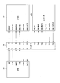
- An information processing system 1 includes, as shown in FIG. 1, a power supply 10, a central processing unit (CPU) 20, a standard device 30, a nonstandard device 40 (an example of a peripheral device including a register), a memory 50 (an example of volatile memory), a storage 60, and a selector 70.
- CPU central processing unit
- standard device 30 an example of a peripheral device including a register
- nonstandard device 40 an example of a peripheral device including a register
- a memory 50 an example of volatile memory
- storage 60 an example of volatile memory
- selector 70 selector
- the information processing system 1 secures in advance in the memory 50 a corresponding memory area in a one-to-one correspondence with the same address as a register provided in the non-standard device 40, and synchronizes data in the corresponding one-to-one memory area. It is. As a result, even when the information processing system 1 is started, the data processing system 1 has almost the same timing as the peripheral device initialized by writing data including the snapshot image information and the initial setting data of the nonstandard device 40 into the main memory.
- peripheral devices with registers can be initialized.
- the snapshot image information is data indicating a predetermined state such as immediately before interruption of the information processing system 1 stored in the non-volatile memory or at the time of factory shipment. The initialization is to set each peripheral device to an operable state.
- the high-speed start is a predetermined state such as a state at the time of shipment from the factory or a state immediately before the power of the device is shut down by starting the information processing system 1 and writing data including snapshot image information to the main memory.
- the information processing system 1 can be started at high speed and the peripheral devices provided with the registers can be initialized, so that the user can start using the information processing system 1 from a predetermined state immediately after the activation.
- the power supply 10 supplies power to each of the CPU 20, the standard device 30, the non-standard device 40, the memory 50, the storage 60, and the selector 70, as shown in FIG.
- the standard device 30 is a peripheral device that is initialized by writing data including snapshot image information to the main memory.
- the standard device 30 can be activated at high speed in a predetermined state by writing data including snapshot image information in the memory 50 by the boot loader.
- the predetermined state is a state such as immediately before the interruption of the processing of the information processing system 1 or at the time of factory shipment.
- the non-standard device 40 is a peripheral device provided with a register.
- the non-standard device 40 becomes operable by writing initialization data indicating initialization to the register.
- the non-standard device 40 comprises a register 401, as shown in FIG.
- the register 401 is a register that holds initial setting data.
- the register 401 includes a reg_adr terminal, a reg_wreq terminal, a reg_wdata terminal, a reg_rreq terminal, a reg_rdata terminal, and a reg_rvalid terminal.
- the reg_adr terminal is a terminal that receives an address at the time of reading or writing of the register 401 from the CPU 20.
- the reg_wreq terminal is a terminal that receives a signal instructing writing to the register 401 from the CPU 20.
- the reg_wdata terminal is a terminal that receives data to be written from the CPU 20 when the reg_wreq terminal receives a signal instructing writing.
- the reg_rreq terminal is a terminal that receives a signal instructing reading from the CPU 20.
- the reg_rdata terminal is a terminal that outputs the data read out to the CPU 20 when the reg_rreq terminal receives a signal instructing reading.
- the reg_rvalid terminal is a signal that specifies data (that is, data to be read) output from the reg_rdata terminal.
- the memory 50 is a main memory used by the CPU 20 for processing.
- the memory 50 is a volatile memory. Data transmission and reception are performed at high speed between the memory 50 and the CPU 20.
- data including snapshot image information stored in the storage 60 and initial setting data of the non-standard device 40 is written to the memory 50.
- the data including the snapshot image information and the initial setting data of the non-standard device 40 includes command information indicating writing and information indicating the address of the writing destination.
- the memory 50 includes a mem_adr terminal, a mem_wreq terminal, a mem_wdata terminal, a mem_rreq terminal, a mem_rdata terminal, and a mem_rvalid terminal.
- the mem_adr terminal is a terminal that receives an address at the time of reading or writing of the memory 50 from the CPU 20.
- the mem_wreq terminal is a terminal that receives a signal instructing writing to the memory 50 from the CPU 20.
- the mem_wdata terminal is a terminal that receives data to be written from the CPU 20 when the mem_wreq terminal receives a signal instructing writing.
- the mem_rreq terminal is a terminal that receives a signal instructing reading from the CPU 20.
- the mem_rdata terminal is a terminal for outputting data read out to the CPU 20 when the mem_rreq terminal receives a signal instructing reading.
- the mem_rvalid terminal is a signal that specifies data (that is, data to be read) output from the mem_rdata terminal.
- the storage 60 is a non-volatile memory.
- the storage 60 stores data including snapshot image information written to the memory 50 at startup and initialization data of the non-standard device 40.
- the storage 60 also stores an OS, an application program, data processed by the application program, and the like.
- the CPU 20 reads and writes data with at least one of the memory 50 and the register 401 via the selector 70.
- the CPU 20 includes an adr terminal, a wreq terminal, a wdata terminal, an rreq terminal, an rdata terminal, and an rvalid terminal.
- the adr terminal is a terminal that outputs an address at the time of reading or writing of at least one of the memory 50 and the register 401.
- the wreq terminal is a terminal that outputs a signal instructing writing to at least one of the memory 50 and the register 401.
- the wdata terminal is a terminal that outputs data to be written when the wreq terminal outputs a signal instructing writing.
- the rreq terminal is a terminal that outputs a signal instructing reading to at least one of the memory 50 and the register 401.
- the rdata terminal is a terminal for receiving data read out when the rreq terminal outputs a signal instructing reading to at least one of the memory 50 and the register 401.
- the rvalid terminal is a signal that specifies data received from the rdata terminal (ie, read data).
- the selector 70 is connected to each of the CPU 20, the memory 50, and the register 401 as shown in FIG.
- the selector 70 has terminals T1, T2, T3, T4, T5, T6, T7, T8, T9, T10, T11, T11, T12, T13, T14, T15, T16. It has a terminal, a T17 terminal, and a T18 terminal.
- the T1 terminal is connected to the adr terminal.
- the T2 terminal is connected to the wreq terminal.
- the T3 terminal is connected to the wdata terminal.
- the T4 terminal is connected to the rreq terminal.
- the T5 terminal is connected to the rdata terminal.
- the T6 terminal is connected to the rvalid terminal.
- the T7 terminal is connected to the mem_adr terminal.
- the T8 terminal is connected to the mem_wreq terminal.
- the T9 terminal is connected to mem_wdata.
- the T10 terminal is connected to the mem_rreq terminal.
- the T11 terminal is connected to the mem_rdata terminal.
- the T12 terminal is connected to the mem_rvalid terminal.
- the T13 terminal is connected to the reg_adr terminal.
- the T14 terminal is connected to the wreg terminal.
- the T15 terminal is connected to reg_wdata.
- the T16 terminal is connected to the reg_rreq terminal.
- the T17 terminal is connected to the reg_rdata terminal.
- the T18 terminal is connected to the reg_rvalid terminal.
- the selector 70 is a hardware-implemented circuit that is logically designed to output or receive signals from the appropriate terminals T7 to T18 in accordance with signals input from the CPU 20. Specifically, for example, when the same address of the memory 50 and the register 401 is input to the T1 terminal and a signal instructing writing is input to the T2 terminal, the selector 70 receives the address input to the T1 terminal. Is output from both the T7 terminal and the T13 terminal. Further, the selector 70 outputs a signal instructing writing, which is input to the T2 terminal, from both the T8 terminal and the T14 terminal. Further, the selector 70 outputs the data input to the T3 terminal to both the T9 terminal and the T15 terminal.
- the selector 70 selects the address input to the T1 terminal as the T7 terminal. Output from Also, the selector 70 outputs the signal instructing writing, which is input to the T2 terminal, from the T8 terminal. Further, the selector 70 outputs the data input to the T3 terminal to the T9 terminal.
- the address input to the T1 terminal is It is output from the T7 terminal and the T13 terminal.
- the signal instructing reading that is input to the T4 terminal is output from the T16 terminal.
- the terminal T17 is connected to the register 401 to acquire data.
- the T9 terminal outputs the data acquired by T17 to the memory 50.
- the register 401 When outputting data from the reg_rdata terminal, the register 401 outputs a “low level signal” for specifying the data to the selector 70 from the reg_rvalid terminal.
- the selector 70 outputs a signal instructing writing from the T8 terminal to the mem_wreg terminal in response to the “Low level signal” for specifying data received at the T18 terminal, and the data stored in the register 401 is stored in the memory 50. Write.
- the signal instructing reading that is input to the T4 terminal is T10. Pinned output.
- the T11 terminal is connected to the memory 50 to acquire data.
- the T5 terminal outputs the data acquired by T11 to the CPU 20.
- the CPU 20 determines at the time of transmission that the data input to the T1 terminal is an address that only the memory 50 has. Therefore, the CPU 20 acquires data from the T5 terminal and completes the data reading.
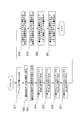
- the CPU 20 outputs the address "m1000" from the adr terminal to the T1 terminal (step S1).
- the CPU 20 outputs data "1234" from the wdata terminal to the T3 terminal (step S2).
- the CPU 20 outputs a “low level signal” instructing writing from the wreq terminal to the T2 terminal (that is, a signal instructing writing is asserted) (step S3).
- the CPU 20 performs the process of step S1 and the process of step S2 almost simultaneously, and outputs a signal instructing writing when the address and data signals are stabilized.
- the process of outputting the address and data at the time of writing by the CPU 20 is performed almost simultaneously even if it is not particularly described. Further, the process of outputting a signal instructing writing at the time of writing is performed by the CPU 20 when the address and data signals are stabilized.
- the selector 70 outputs the address input from the T1 terminal from the T7 terminal to the mem_adr terminal (step S4). Further, the selector 70 outputs a signal instructing writing, which is input from the T2 terminal, to the mem_wreq terminal from the T8 terminal (step S5). Further, the selector 70 outputs the data input from the T3 terminal to the mem_wdata terminal from the T9 terminal (step S6).
- the memory 50 receives an address “m1000”, a “low level signal” instructing writing, and data “1234” from the selector 70.
- the memory 50 writes the data "1234" in the memory area of the address "m1000” in response to the signal instructing the writing (step S7).
- the selector 70 is a circuit realized by hardware as described above. Therefore, when the selector 70 receives an address, data, a signal instructing writing, a signal instructing reading, etc. from the CPU 20, the processing is completed almost simultaneously with receiving the signal, and the processed signal is output from an appropriate terminal. Do.
- the selector 70 completes the processing substantially simultaneously with receiving the input signal, and outputs the processed signal from an appropriate terminal.
- the selector 70 outputs the address input from the T1 terminal to the mem_adr terminal from the T7 terminal (step S14).
- the selector 70 outputs the address input from the T1 terminal to the reg_adr terminal from the T13 terminal (step S15).
- the selector 70 outputs the data input from the T3 terminal to the mem_wdata terminal from the T9 terminal (step S16).
- the selector 70 outputs the data input from the T3 terminal to the reg_wdata terminal from the T15 terminal (step S17).
- the selector 70 outputs a signal instructing writing, which is input from the T2 terminal, from the T8 terminal to the mem_wreq terminal (step S18).
- the selector 70 outputs the signal instructing writing, which is input from the T2 terminal, from the T14 terminal to the reg_wreq terminal (step S19).
- the processes of steps S14 and S15, S16 and S17, and S18 and S19 performed by the selector 70 are performed in parallel.
- the memory 50 receives, from the selector 70, an address "m 9000", a "low level signal” instructing writing, and data "5678".
- the memory 50 writes the data "5678" in the memory area of the address "m9000” in response to the signal instructing the writing (step S20).
- the register 401 receives an address “m 9000”, a “low level signal” instructing writing, and data “5678” from the selector 70.
- the register 401 writes the data "5678" in the memory area of the address "m9000” in response to the signal instructing the writing (step S21).
- the information processing system 1 stores data having snapshot image information stored in the storage 60 and initial setting data of the non-standard device 40 in the same memory as the address of the register 401. Perform processing to write to the 50 addresses.
- the initial setting data is written to the register 401. Accordingly, the non-standard device 40 becomes operable almost simultaneously as the snapshot image information is written to the memory 50 and the standard device 30 becomes operable.
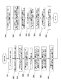
- Reading data from memory 50 Reading of data from the memory 50 shown in FIG. 3C, that is, the data "1234" from the memory area of the address of the memory 50 different from the address of the register 401 (for example, the address "m1000" shown in FIG. 3). The reading will be described using the processing flow shown in FIG.
- the CPU 20 outputs the address "m1000" from the adr terminal to the T1 terminal (step S31). Further, the CPU 20 outputs a “low level signal” instructing reading from the rreq terminal to the T4 terminal (that is, a signal instructing reading is asserted) (step S32).
- the selector 70 outputs the address input from the T1 terminal to the mem_adr terminal from the T7 terminal (step S33). Further, the selector 70 outputs a “low level signal” instructing reading out input from the T4 terminal to the mem_rreq terminal from the T10 terminal (step S34).
- the memory 50 receives, from the selector 70, the address "m1000" and a "low level signal” instructing reading.
- the memory 50 outputs the data "1234" of the memory area of the address "m1000" from the mem_rdata terminal to the terminal 11 in response to the "low level signal” instructing the reading (step S35). Further, the memory 50 outputs the “low level signal” for specifying the data “1234” from the mem_rvalid terminal to the T12 terminal in response to the “low level signal” instructing the reading (step S36).
- the selector 70 outputs the data input to the terminal 11 from the T5 terminal to the rdata terminal (step S37). Further, the selector 70 outputs a “low level signal” that specifies the data input to the terminal T12 from the T6 terminal to the rvalid terminal (step S38).
- the CPU 20 acquires data “1234” received by the rdata terminal while the rvalid terminal receives the “low level signal” as read data (step S39).
- Reading data from register 401 Reading of data from the register 401 shown in FIG. 3D, that is, data "9876” from the memory area of the address of the register 401 where the same address exists in the memory 50 (for example, the address "m8000" shown in FIG. 3). The “read out” will be described using the process flow shown in FIG.
- the CPU 20 outputs the address "m8000" from the adr terminal to the T1 terminal (step S41). Then, the CPU 20 outputs a "low level signal” instructing reading from the rreq terminal to the T4 terminal (that is, a signal instructing reading is asserted) (step S42).
- the selector 70 outputs the address input from the T1 terminal to the mem_adr terminal from the T7 terminal and to the reg_adr terminal from the T13 terminal (step S43).
- the selector 70 outputs, from the T16 terminal to the reg_rreq terminal, a signal for instructing reading which is input from the T4 terminal (step S44).
- the register 401 receives an address “m 8000” and a “low level signal” instructing reading from the selector 70.
- the memory 50 receives the address "m8000” from the selector 70 (step S45).
- the register 401 outputs data “9876” in the memory area of the address “m8000” from the reg_rdata terminal to the terminal 17 in response to the signal instructing reading (step S46). Further, the register 401 outputs a “low level signal” for specifying the data “9876” from the reg_rvalid terminal to the T18 terminal in response to the signal instructing the reading (step S47).
- the selector 70 outputs the data input to the terminal 17 from the T5 terminal to the rdata terminal and from the T9 terminal to the mem_wdata terminal (step S48). Further, the selector 70 outputs a “low level signal” for specifying data input to the terminal T18 from the T6 terminal to the rvalid terminal (step S49).
- the CPU 20 acquires data “9876” received by the rdata terminal while the rvalid terminal receives the “low level signal” as read data (step S50).
- the selector 70 When the selector 70 outputs a “low level signal” from the T6 terminal to the rvalid terminal, the selector 70 outputs a signal instructing writing from the T8 terminal to the mem_wreq terminal (step S51).
- the memory 50 receives a “low level signal” instructing writing.
- the memory 50 writes the data "9876" in the memory area of the address "m8000" received from the selector 70 in response to the signal instructing the writing (step S52).
- the register 401 When the transmission of the data "9876" is completed, the register 401 outputs a "high level signal" from the reg_rvalid terminal to the T18 terminal (step S53). That is, when the register 401 outputs the “high level signal” from the reg_rvalid terminal, the data transmission has been completed. Therefore, at the stage when the register 401 outputs a "high level signal” from the reg_rvalid terminal in the process of step S49, the data read from the register 401 is transmitted to the memory 50 and is used as data written in the memory 50. It is decided. Note that the process performed by the register 401 in the process of reading data from the register 401 is completed by the process of step S51. In the process of reading data from the register 401, when the register 401 ends the process, the data output from the reg_rdata by the register 401 becomes an undefined value.
- step S54 When the T18 terminal receives the “high level signal”, the selector 70 outputs the “high level signal” from the T8 terminal to the mem_wreq terminal and from the T6 terminal to the rvalid terminal (step S54).
- step S54 the writing process to the memory 50 for synchronizing data with the register 401 in the process of reading data from the register 401 is completed.
- the data input to the mem_wdata terminal of the memory 50 has an undefined value.
- the CPU 20 receives the “high level signal” at the rvalid terminal, the CPU 20 ends the process of reading data from the register 401.
- the CPU 20 ends the process of reading data from the register 401 in the process of reading data from the register 401, the data input to the rdata terminal of the CPU 20 becomes an undefined value.
- the CPU 20 ends the process of reading data from the register 401, the CPU 20 outputs a "high level signal" from the rreq terminal to the T4 terminal (step S55).
- step S56 the process of reading data from the register 401 performed by the information processing system 1 ends.
- the address output from the adr terminal of the CPU 20 becomes undefined, the address input to the reg_adr terminal and the mem_adr terminal becomes undefined, and all addresses are open. Be done.
- the CPU 20 selects an address and a write instruction signal instructing writing data to the address or a read instruction signal instructing reading data from the address.
- Output to The selector 70 is configured by hardware such that an output destination of data input from the CPU 20 is determined according to an address, a write instruction signal, and a read instruction signal.
- the memory 50 stores data including snapshot image information and initial setting data of the non-standard device 40 provided with the register 401 when the information processing system 1 is started based on a signal output from the selector 70.
- the register 401 has the same address as the address of the memory area in which the memory 50 stores initial setting data.
- the information processing system 1 When the information processing system 1 starts up, the information processing system 1 has data including snapshot image information and initial setting data of the non-standard device 40 including the register 401 at the same address of the memory 50 as the address of the register 401. Write to the memory area of By doing this, when the information processing system 1 starts up, at the same time as snapshot image information is reproduced in the memory 50, initial setting data is written to the register 401. Accordingly, the non-standard device 40 becomes operable almost simultaneously as the snapshot image information is written to the memory 50 and the standard device 30 becomes operable. As described above, when the information processing system 1 is activated by the information processing system 1, the non-standard device 40 including the register 401 can be immediately initialized.
- the register 401 has been described as being capable of both writing and reading. However, some of the registers 401 may be writable only.
- the register 401 can only write, the process of replacing the register 401 and the memory 50 in the above (reading of data from the register 401), reading data from the memory 50, and writing the read data into the register 401 (register The data in the memory 50 and the register 401 can be synchronized by performing the same process as in the process of reading data from 401). Also, the CPU 20 can read data to be stored in the register 401 from the memory 50.
- the order of the processes may be switched as long as the appropriate process is performed.
- the memory, the storage, the storage unit including the register, and the other storage devices in the embodiment of the present invention may be provided anywhere as long as appropriate transmission and reception of information is performed.
- each of the storage unit and the other storage devices may be present in a distributed manner in a range where appropriate transmission and reception of information is performed, and the data may be distributed and stored.
- FIG. 8 is a schematic block diagram showing the configuration of a computer according to at least one embodiment.
- the computer 5 includes a CPU 6, a main memory 7, a storage 8 and an interface 9, as shown in FIG.
- each of the above-described standard device 30, non-standard device 40, and other control devices is implemented in the computer 5.
- the operation of each processing unit described above is stored in the storage 8 in the form of a program.
- the CPU 6 reads a program from the storage 8 and develops it in the main memory 7 and executes the above processing according to the program. Further, the CPU 6 secures, in the main memory 7, a memory area corresponding to each storage unit described above according to a program.
- Examples of the storage 8 include a hard disk drive (HDD), a solid state drive (SSD), a magnetic disk, an optical magnetic disk, a compact disc read only memory (CD-ROM), and a digital versatile disc read only memory (DVD-ROM). , Semiconductor memory and the like.
- the storage 8 may be internal media directly connected to the bus of the computer 5 or may be external media connected to the computer 5 via the interface 9 or a communication line.
- the program is distributed to the computer 5 by a communication line, the computer 5 that has received the distribution may expand the program in the main memory 7 and execute the above processing.
- storage 8 is a non-transitory tangible storage medium.
- the program may realize part of the functions described above.
- the program may be a file capable of realizing the above-described functions in combination with a program already recorded in a computer system, a so-called difference file (difference program).
- the peripheral device provided with the register can be immediately initialized.
Landscapes
- Engineering & Computer Science (AREA)
- Software Systems (AREA)
- Theoretical Computer Science (AREA)
- Physics & Mathematics (AREA)
- General Engineering & Computer Science (AREA)
- General Physics & Mathematics (AREA)
- Computer Security & Cryptography (AREA)
- Debugging And Monitoring (AREA)
- Stored Programmes (AREA)
- Techniques For Improving Reliability Of Storages (AREA)
Abstract
Description
特許文献1には、関連する技術として、システムの中断前の揮発性メモリの記憶状態、周辺デバイスのレジスタ値、及び、プロセッサのレジスタ値を表すデータを不揮発性メモリに格納し、システムの起動時にOS(Operating System)はカーネル機能によって不揮発性メモリに格納したデータを用いてシステムの中断前の状態を再現することで、情報処理システムを直ちに初期化する技術が記載されている。
そのため、情報処理システムが起動する際に、レジスタを備える周辺デバイスを直ちに初期化することのできる技術が求められている。
情報処理システムは、情報処理システムが起動する際に、スナップショットイメージ情報とレジスタを備える非標準デバイスの初期設定データとを含むデータを、レジスタのアドレスと同一のアドレスの揮発性メモリのメモリ領域へ書き込む処理を行う。こうすることで、情報処理システムが起動する際に、揮発性メモリにおいてスナップショットイメージ情報が再現されると同時に、レジスタに初期設定データが書き込まれる。したがって、スナップショットイメージ情報が揮発性メモリに書き込まれ、標準デバイスが動作可能な状態になるのとほぼ同時に、非標準デバイスは、動作可能な状態となる。
このように、情報処理システムによって、情報処理システムが起動する際に、レジスタを備える周辺デバイスを直ちに初期化することができる。
情報処理システムは、揮発性メモリとレジスタの両方に、アドレスと書込みデータとを入力する。そのため、情報処理システムは、揮発性メモリとレジスタのそれぞれにおいて同一のアドレスを示すメモリ領域に同一の書込みデータが書き込む。こうすることで、情報処理システムは、同一のアドレスを示すメモリ領域において、揮発性メモリとレジスタとで同期をとることができる。
情報処理システムは、揮発性メモリとレジスタの両方に共通するアドレスからデータを読み出す場合、レジスタから書込みデータを取得する。そして、情報処理システムは、レジスタから取得した読出しデータに対応するアドレスと同一のアドレスの揮発性メモリのメモリ領域に読出しデータを書き込む。こうすることで、情報処理システムは、同一のアドレスを示すメモリ領域において、揮発性メモリとレジスタとで同期をとることができる。
情報処理システムは、揮発性メモリとレジスタの両方に共通するアドレスからデータを読み出す場合、揮発性メモリから書込みデータを取得する。そして、情報処理システムは、揮発性メモリから取得した読出しデータに対応するアドレスと同一のアドレスのレジスタのメモリ領域に読出しデータを書き込む。こうすることで、情報処理システムは、同一のアドレスを示すメモリ領域において、揮発性メモリとレジスタとで同期をとることができる。
情報処理システムによる情報処理方法は、揮発性メモリとレジスタの両方に共通するアドレスからデータを読み出す場合、レジスタから書込みデータを取得する。そして、情報処理システムによる情報処理方法は、レジスタから取得した読出しデータに対応するアドレスと同一のアドレスの揮発性メモリのメモリ領域に読出しデータを書き込む。こうすることで、情報処理システムによる情報処理方法は、同一のアドレスを示すメモリ領域において、揮発性メモリとレジスタとで同期をとることができる。
(情報処理システムの構成)
以下、本発明の一実施形態による情報処理システムの構成について説明する。
本発明の一実施形態による情報処理システム1は、図1に示すように、電源10、CPU(Central Processing Unit)20、標準デバイス30、非標準デバイス40(レジスタを備える周辺デバイスの一例)、メモリ50(揮発性メモリの一例)、ストレージ60、セレクタ70を備える。
CPU20は、セレクタ70を介して、メモリ50及びレジスタ401の少なくとも一方との間でデータの読み書きを行う。CPU20は、図2に示すように、adr端子、wreq端子、wdata端子、rreq端子、rdata端子、rvalid端子を備える。adr端子は、メモリ50及びレジスタ401の少なくとも一方についての読み出しまたは書き込み時のアドレスを出力する端子である。wreq端子は、メモリ50及びレジスタ401の少なくとも一方へ書込みを指示する信号を出力する端子である。wdata端子は、wreq端子が書込みを指示する信号を出力したときに書き込むデータを出力する端子である。rreq端子は、メモリ50及びレジスタ401の少なくとも一方へ読出しを指示する信号を出力する端子である。rdata端子は、rreq端子がメモリ50及びレジスタ401の少なくとも一方へ読出しを指示する信号を出力したときに読み出されたデータを受ける端子である。rvalid端子は、rdata端子から受けるデータ(すなわち読み出されたデータ)を特定する信号である。
セレクタ70は、図2に示すように、CPU20、メモリ50、レジスタ401のそれぞれに接続される。セレクタ70は、T1端子、T2端子、T3端子、T4端子、T5端子、T6端子、T7端子、T8端子、T9端子、T10端子、T11端子、T12端子、T13端子、T14端子、T15端子、T16端子、T17端子、T18端子を備える。T1端子は、adr端子に接続される。T2端子は、wreq端子に接続される。T3端子は、wdata端子に接続される。T4端子は、rreq端子に接続される。T5端子は、rdata端子に接続される。T6端子は、rvalid端子に接続される。T7端子は、mem_adr端子に接続される。T8端子は、mem_wreq端子に接続される。T9端子は、mem_wdataに接続される。T10端子は、mem_rreq端子に接続される。T11端子は、mem_rdata端子に接続される。T12端子は、mem_rvalid端子に接続される。T13端子は、reg_adr端子に接続される。T14端子は、wreg端子に接続される。T15端子は、reg_wdataに接続される。T16端子はreg_rreq端子に接続される。T17端子は、reg_rdata端子に接続される。T18端子は、reg_rvalid端子に接続される。
具体的には、例えば、T1端子にメモリ50とレジスタ401とが有する同一のアドレスが入力され、T2端子に書込みを指示する信号が入力された場合、セレクタ70は、T1端子に入力されたアドレスをT7端子とT13端子の両方から出力する。また、セレクタ70は、T2端子に入力された書込みを指示する信号を、T8端子とT14端子の両方から出力する。また、セレクタ70は、T3端子に入力されたデータをT9端子とT15端子の両方に出力する。
次に、本発明の一実施形態による情報処理システム1の処理について説明する。
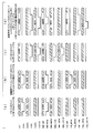
ここでは、図3(a)~(d)に示す4つの場合について、情報処理システム1の処理の処理を説明する。
図3(a)に示すメモリ50へのデータの書き込み、すなわち、レジスタ401のアドレスとは異なるメモリ50のアドレス(例えば、図3に示すアドレス“m1000”)のメモリ領域へのデータ“1234”の書き込みについて図4に示す処理フローを用いて説明する。
図3(b)に示すレジスタ401へのデータの書き込み、すなわち、レジスタ401のアドレスと同一のメモリ50のアドレス(例えば、図3に示すアドレス“m9000”)のメモリ領域へのデータ“5678”の書き込みについて図5に示す処理フローを用いて説明する。
CPU20は、adr端子からT1端子へアドレス“m9000”を出力する(ステップS11)。また、CPU20は、wdata端子からT3端子へデータ“5678”を出力する(ステップS12)。そして、CPU20は、wreq端子からT2端子へ書込みを指示する“Lowレベルの信号”を出力する(ステップS13)。
図3(c)に示すメモリ50からのデータの読み出し、すなわち、レジスタ401のアドレスとは異なるメモリ50のアドレス(例えば、図3に示すアドレス“m1000”)のメモリ領域からのデータ“1234”の読み出しについて図6に示す処理フローを用いて説明する。
CPU20は、adr端子からT1端子へアドレス“m1000”を出力する(ステップS31)。また、CPU20は、rreq端子からT4端子へ読出しを指示する“Lowレベルの信号”を出力する(すなわち、読出しを指示する信号がアサートされる)(ステップS32)。
メモリ50は、セレクタ70から、アドレス“m1000”、読出しを指示する“Lowレベルの信号”を受ける。メモリ50は、読出しを指示する“Lowレベルの信号”に応じて、アドレス“m1000”のメモリ領域のデータ“1234”をmem_rdata端子から端子11へ出力する(ステップS35)。また、メモリ50は、読出しを指示する“Lowレベルの信号”に応じて、mem_rvalid端子からT12端子へデータ“1234”を特定する“Lowレベルの信号”を出力する(ステップS36)。
CPU20は、rvalid端子が“Lowレベルの信号”を受けている間にrdata端子が受けたデータ“1234”を読み出したデータとして取得する(ステップS39)。
図3(d)に示すレジスタ401からのデータの読み出し、すなわち、メモリ50において同一のアドレスが存在するレジスタ401のアドレス(例えば、図3に示すアドレス“m8000”)のメモリ領域からのデータ“9876”の読み出しについて図7に示す処理フローを用いて説明する。
メモリ50は、書込みを指示する“Lowレベルの信号”を受ける。メモリ50は、書込みを指示する信号に応じて、セレクタ70から受けたアドレス“m8000”のメモリ領域にデータ“9876”を書き込む(ステップS52)。
以上、本発明の一実施形態による情報処理システム1について説明した。
本発明の一実施形態による情報処理システム1では、CPU20は、アドレスと、そのアドレスへデータを書き込むことを指示する書込み指示信号またはそのアドレスからデータを読み出すことを指示する読出し指示信号とをセレクタ70に出力する。セレクタ70は、アドレス、書込み指示信号及び読出し指示信号に応じて、CPU20から入力されたデータの出力先が決定されるようにハードウェアで構成される。メモリ50は、セレクタ70が出力する信号に基づいて、情報処理システム1が起動する際に、スナップショットイメージ情報とレジスタ401を備える非標準デバイス40の初期設定データとを含むデータを記憶する。レジスタ401は、メモリ50が初期設定データを記憶するメモリ領域のアドレスと同一のアドレスを有する。
このように、情報処理システム1によって、情報処理システム1が起動する際に、レジスタ401を備える非標準デバイス40を直ちに初期化することができる。
なお、本発明の別の実施形態による情報処理システム1において、レジスタ401は、書き込み及び読み出しの両方が可能であるものとして説明した。しかしながら、レジスタ401の中には、書き込みのみが可能であるものも存在する。
レジスタ401が書き込みのみ可能な場合、上述の(レジスタ401からのデータの読み出し)におけるレジスタ401とメモリ50とを入れ替え、メモリ50からデータを読み出し、読み出したデータをレジスタ401に書き込む処理を、(レジスタ401からのデータの読み出し)における処理と同様に行うことで、メモリ50とレジスタ401のデータを同期することができる。また、CPU20は、レジスタ401が記憶すべきデータをメモリ50から読み出すことができる。
図8は、少なくとも1つの実施形態に係るコンピュータの構成を示す概略ブロック図である。
コンピュータ5は、図8に示すように、CPU6、メインメモリ7、ストレージ8、インターフェース9を備える。
例えば、上述の標準デバイス30、非標準デバイス40、その他の制御装置のそれぞれは、コンピュータ5に実装される。そして、上述した各処理部の動作は、プログラムの形式でストレージ8に記憶されている。CPU6は、プログラムをストレージ8から読み出してメインメモリ7に展開し、当該プログラムに従って上記処理を実行する。また、CPU6は、プログラムに従って、上述した各記憶部に対応するメモリ領域をメインメモリ7に確保する。
6、20・・・CPU
7・・・メインメモリ
8・・・ストレージ
9・・・インターフェース
10・・・電源
30・・・標準デバイス
40・・・非標準デバイス
50・・・メモリ
60・・・ストレージ
70・・・セレクタ
401・・・レジスタ
Claims (5)
- アドレスと、前記アドレスへデータを書き込むことを指示する書込み指示信号または前記アドレスからデータを読み出すことを指示する読出し指示信号とをセレクタに出力するCPU(Central Processing Unit)と、
前記アドレス、前記書込み指示信号及び前記読出し指示信号に応じて、前記CPUから入力されたデータの出力先が決定されるようにハードウェアで構成された前記セレクタと、
前記セレクタが出力する信号に基づいて、情報処理システムが起動する際に、スナップショットイメージ情報とレジスタを備える非標準デバイスの初期設定データとを含むデータを記憶する揮発性メモリと、
前記揮発性メモリが前記初期設定データを記憶するメモリ領域のアドレスと同一のアドレスを有する前記レジスタと、
を備える情報処理システム。 - 前記セレクタは、
前記揮発性メモリと前記レジスタとが有する同一のアドレスが入力され、前記書込み指示信号が入力された場合、前記同一のアドレスを前記揮発性メモリと前記レジスタとに出力し、前記揮発性メモリと前記レジスタの両方に対して書込みデータを出力する、
請求項1に記載の情報処理システム。 - 前記セレクタは、
前記揮発性メモリと前記レジスタとが有する同一のアドレスが入力され、前記読出し指示信号が入力された場合、前記同一のアドレスを前記レジスタに出力し、
前記レジスタから読出しデータを取得し、前記書込み指示信号と、前記レジスタから取得した読出しデータとを前記揮発性メモリに出力する、
請求項1または請求項2に記載の情報処理システム。 - 前記セレクタは、
前記揮発性メモリと前記レジスタとが有する同一のアドレスが入力され、前記読出し指示信号が入力された場合、前記同一のアドレスを前記メモリに出力し、
前記メモリから読出しデータを取得し、前記書込み指示信号と、前記メモリから取得した読出しデータとを前記レジスタに出力する、
請求項1または請求項2に記載の情報処理システム。 - CPU、アドレス、書込み指示信号及び読出し指示信号に応じて、前記CPUから入力されたデータの出力先が決定されるようにハードウェアで構成されたセレクタ、揮発性メモリ、及び前記揮発性メモリがレジスタを備える非標準デバイスの初期設定データを記憶するメモリ領域のアドレスと同一のアドレスを有するレジスタ、を有する情報処理システムによる情報処理方法であって、
前記CPUは、
前記アドレスと、前記アドレスへデータを書き込むことを指示する前記書込み指示信号または前記アドレスからデータを読み出すことを指示する前記読出し指示信号とを前記セレクタに出力し、
前記揮発性メモリは、
前記セレクタが出力する信号に基づいて、前記情報処理システムが起動する際に、スナップショットイメージ情報と前記初期設定データとを含むデータを記憶する、
情報処理システムによる情報処理方法。
Priority Applications (6)
| Application Number | Priority Date | Filing Date | Title |
|---|---|---|---|
| PCT/JP2017/041548 WO2019097693A1 (ja) | 2017-11-17 | 2017-11-17 | 情報処理システム及び情報処理システムによる情報処理方法 |
| SG11202004378VA SG11202004378VA (en) | 2017-11-17 | 2017-11-17 | Information processing system and information processing method to be executed by information processing system |
| GB2006897.9A GB2581719B (en) | 2017-11-17 | 2017-11-17 | Information processing system and information processing method to be executed by information processing system |
| US16/763,652 US11249904B2 (en) | 2017-11-17 | 2017-11-17 | Information processing system and information processing method to be executed by information processing system |
| KR1020207013538A KR102281418B1 (ko) | 2017-11-17 | 2017-11-17 | 정보 처리 시스템 및 정보 처리 시스템에 의한 정보 처리 방법 |
| JP2019553644A JP6966568B2 (ja) | 2017-11-17 | 2017-11-17 | 情報処理システム及び情報処理システムによる情報処理方法 |
Applications Claiming Priority (1)
| Application Number | Priority Date | Filing Date | Title |
|---|---|---|---|
| PCT/JP2017/041548 WO2019097693A1 (ja) | 2017-11-17 | 2017-11-17 | 情報処理システム及び情報処理システムによる情報処理方法 |
Publications (1)
| Publication Number | Publication Date |
|---|---|
| WO2019097693A1 true WO2019097693A1 (ja) | 2019-05-23 |
Family
ID=66539430
Family Applications (1)
| Application Number | Title | Priority Date | Filing Date |
|---|---|---|---|
| PCT/JP2017/041548 Ceased WO2019097693A1 (ja) | 2017-11-17 | 2017-11-17 | 情報処理システム及び情報処理システムによる情報処理方法 |
Country Status (6)
| Country | Link |
|---|---|
| US (1) | US11249904B2 (ja) |
| JP (1) | JP6966568B2 (ja) |
| KR (1) | KR102281418B1 (ja) |
| GB (1) | GB2581719B (ja) |
| SG (1) | SG11202004378VA (ja) |
| WO (1) | WO2019097693A1 (ja) |
Families Citing this family (1)
| Publication number | Priority date | Publication date | Assignee | Title |
|---|---|---|---|---|
| US12142338B2 (en) * | 2021-01-19 | 2024-11-12 | Alibaba Group Holding Limited | Memory priming and initialization systems and methods |
Citations (3)
| Publication number | Priority date | Publication date | Assignee | Title |
|---|---|---|---|---|
| JPS62123545A (ja) * | 1985-11-22 | 1987-06-04 | Nec Home Electronics Ltd | デ−タ入出力装置 |
| JPH06131241A (ja) * | 1992-10-19 | 1994-05-13 | Fujitsu Ltd | データ処理装置 |
| JP2015156205A (ja) * | 2014-01-20 | 2015-08-27 | キヤノン株式会社 | 情報処理装置およびその制御方法 |
Family Cites Families (10)
| Publication number | Priority date | Publication date | Assignee | Title |
|---|---|---|---|---|
| US4675813A (en) * | 1985-01-03 | 1987-06-23 | Northern Telecom Limited | Program assignable I/O addresses for a computer |
| US6212609B1 (en) * | 1997-06-30 | 2001-04-03 | Intel Corporation | Alternate access mechanism for saving and restoring state of read-only register |
| KR100453262B1 (ko) | 1998-08-10 | 2004-10-15 | 미크론 테크놀로지,인코포레이티드 | 주변 장치의 상태 정보를 관리 및 갱신하는 방법, 컴퓨터 시스템, 그리고 프로세서 내의 장치 |
| JP4961781B2 (ja) * | 2006-03-14 | 2012-06-27 | ソニー株式会社 | 情報処理装置、その起動方法およびプログラム |
| US8825912B2 (en) | 2008-11-12 | 2014-09-02 | Microchip Technology Incorporated | Dynamic state configuration restore |
| JP6160273B2 (ja) * | 2013-06-06 | 2017-07-12 | 富士通株式会社 | 半導体回路装置、及び、電子装置 |
| US9916173B2 (en) * | 2013-11-25 | 2018-03-13 | Red Hat Israel, Ltd. | Facilitating execution of MMIO based instructions |
| JP6294732B2 (ja) * | 2014-03-31 | 2018-03-14 | 株式会社メガチップス | データ転送制御装置及びメモリ内蔵装置 |
| TWI564802B (zh) * | 2015-12-14 | 2017-01-01 | 財團法人工業技術研究院 | 初始化週邊裝置之方法與使用此方法之電子裝置 |
| US10223149B2 (en) * | 2016-12-15 | 2019-03-05 | Intel Corporation | Implementing device models for virtual machines with reconfigurable hardware |
-
2017
- 2017-11-17 JP JP2019553644A patent/JP6966568B2/ja active Active
- 2017-11-17 GB GB2006897.9A patent/GB2581719B/en active Active
- 2017-11-17 SG SG11202004378VA patent/SG11202004378VA/en unknown
- 2017-11-17 KR KR1020207013538A patent/KR102281418B1/ko not_active Expired - Fee Related
- 2017-11-17 US US16/763,652 patent/US11249904B2/en not_active Expired - Fee Related
- 2017-11-17 WO PCT/JP2017/041548 patent/WO2019097693A1/ja not_active Ceased
Patent Citations (3)
| Publication number | Priority date | Publication date | Assignee | Title |
|---|---|---|---|---|
| JPS62123545A (ja) * | 1985-11-22 | 1987-06-04 | Nec Home Electronics Ltd | デ−タ入出力装置 |
| JPH06131241A (ja) * | 1992-10-19 | 1994-05-13 | Fujitsu Ltd | データ処理装置 |
| JP2015156205A (ja) * | 2014-01-20 | 2015-08-27 | キヤノン株式会社 | 情報処理装置およびその制御方法 |
Also Published As
| Publication number | Publication date |
|---|---|
| KR20200066698A (ko) | 2020-06-10 |
| US20200278928A1 (en) | 2020-09-03 |
| KR102281418B1 (ko) | 2021-07-23 |
| JPWO2019097693A1 (ja) | 2020-11-26 |
| JP6966568B2 (ja) | 2021-11-17 |
| US11249904B2 (en) | 2022-02-15 |
| SG11202004378VA (en) | 2020-06-29 |
| GB2581719B (en) | 2022-03-09 |
| GB2581719A (en) | 2020-08-26 |
| GB202006897D0 (en) | 2020-06-24 |
Similar Documents
| Publication | Publication Date | Title |
|---|---|---|
| US20140181499A1 (en) | Method for improving booting of a computing device | |
| JP6966568B2 (ja) | 情報処理システム及び情報処理システムによる情報処理方法 | |
| US20160350131A1 (en) | Booting device and operating method thereof | |
| US10168958B2 (en) | Information processing system, method in information processing system, and storage medium | |
| CN108268280B (zh) | 半导体装置的处理器及其操作方法 | |
| JP7018067B2 (ja) | 情報処理システム、情報処理方法及びプログラム | |
| CN101796479B (zh) | 具有改善缓冲器容量的使用的大容量存储系统 | |
| EP2735965A2 (en) | Resume method and information processing device | |
| HK40026730A (en) | Information processing system and information processing method to be executed by information processing system | |
| JP7609469B2 (ja) | 処理装置、処理システム、処理方法、およびプログラム | |
| JP7161125B2 (ja) | 情報処理システム、情報処理装置及び情報処理プログラム | |
| US7447893B2 (en) | Method and system for updating boot block BIOS program | |
| JP2016151803A (ja) | ストレージ制御装置、ストレージ制御プログラム、およびストレージ制御方法 | |
| CN107025144B (zh) | 用于写入以及读取数据集的方法 | |
| JP2006331221A (ja) | データ転送装置及びデータ転送方法 | |
| JP2020003983A (ja) | 制御システムおよび電子機器 | |
| JP2006048369A (ja) | カード型メモリのインターフェイス回路、その回路を搭載したasic、及びそのasicを搭載した画像形成装置 | |
| JP2020087021A (ja) | 情報処理装置、画像形成装置およびプログラム | |
| JPWO2018186454A1 (ja) | 情報処理装置 | |
| JPH06282456A (ja) | 疑似動作装置 | |
| JP2014174881A (ja) | 情報処理装置、及び情報処理方法、プログラム |
Legal Events
| Date | Code | Title | Description |
|---|---|---|---|
| 121 | Ep: the epo has been informed by wipo that ep was designated in this application |
Ref document number: 17932298 Country of ref document: EP Kind code of ref document: A1 |
|
| ENP | Entry into the national phase |
Ref document number: 202006897 Country of ref document: GB Kind code of ref document: A Free format text: PCT FILING DATE = 20171117 |
|
| ENP | Entry into the national phase |
Ref document number: 20207013538 Country of ref document: KR Kind code of ref document: A |
|
| ENP | Entry into the national phase |
Ref document number: 2019553644 Country of ref document: JP Kind code of ref document: A |
|
| NENP | Non-entry into the national phase |
Ref country code: DE |
|
| 122 | Ep: pct application non-entry in european phase |
Ref document number: 17932298 Country of ref document: EP Kind code of ref document: A1 |