WO2019093444A1 - Optical laminate film, and organic electroluminescent display device - Google Patents
Optical laminate film, and organic electroluminescent display device Download PDFInfo
- Publication number
- WO2019093444A1 WO2019093444A1 PCT/JP2018/041559 JP2018041559W WO2019093444A1 WO 2019093444 A1 WO2019093444 A1 WO 2019093444A1 JP 2018041559 W JP2018041559 W JP 2018041559W WO 2019093444 A1 WO2019093444 A1 WO 2019093444A1
- Authority
- WO
- WIPO (PCT)
- Prior art keywords
- circularly polarized
- polarized light
- layer
- separation layer
- liquid crystal
- Prior art date
Links
- 230000003287 optical effect Effects 0.000 title claims abstract description 59
- 239000005001 laminate film Substances 0.000 title claims abstract description 10
- 238000000926 separation method Methods 0.000 claims abstract description 261
- 150000001875 compounds Chemical class 0.000 claims abstract description 106
- 239000004986 Cholesteric liquid crystals (ChLC) Substances 0.000 claims abstract description 84
- 239000004973 liquid crystal related substance Substances 0.000 claims abstract description 71
- 230000010287 polarization Effects 0.000 claims abstract description 16
- 230000005540 biological transmission Effects 0.000 claims abstract description 12
- 239000004985 Discotic Liquid Crystal Substance Substances 0.000 claims description 17
- 239000006185 dispersion Substances 0.000 claims description 10
- 230000001747 exhibiting effect Effects 0.000 abstract 1
- 239000010410 layer Substances 0.000 description 441
- 239000010408 film Substances 0.000 description 193
- 238000005401 electroluminescence Methods 0.000 description 159
- 239000011295 pitch Substances 0.000 description 31
- 230000008859 change Effects 0.000 description 29
- 238000000576 coating method Methods 0.000 description 25
- 239000011248 coating agent Substances 0.000 description 24
- 238000002360 preparation method Methods 0.000 description 23
- 239000005268 rod-like liquid crystal Substances 0.000 description 21
- 239000000758 substrate Substances 0.000 description 18
- 230000008033 biological extinction Effects 0.000 description 17
- 239000000243 solution Substances 0.000 description 15
- ZWEHNKRNPOVVGH-UHFFFAOYSA-N 2-Butanone Chemical compound CCC(C)=O ZWEHNKRNPOVVGH-UHFFFAOYSA-N 0.000 description 12
- 230000000875 corresponding effect Effects 0.000 description 11
- UWCWUCKPEYNDNV-LBPRGKRZSA-N 2,6-dimethyl-n-[[(2s)-pyrrolidin-2-yl]methyl]aniline Chemical compound CC1=CC=CC(C)=C1NC[C@H]1NCCC1 UWCWUCKPEYNDNV-LBPRGKRZSA-N 0.000 description 9
- 239000004372 Polyvinyl alcohol Substances 0.000 description 9
- 238000004519 manufacturing process Methods 0.000 description 9
- 239000000203 mixture Substances 0.000 description 9
- 229920002451 polyvinyl alcohol Polymers 0.000 description 9
- 239000000654 additive Substances 0.000 description 8
- 230000000996 additive effect Effects 0.000 description 8
- 230000007423 decrease Effects 0.000 description 8
- 238000011156 evaluation Methods 0.000 description 8
- 239000011521 glass Substances 0.000 description 8
- 238000002834 transmittance Methods 0.000 description 8
- 230000000694 effects Effects 0.000 description 7
- 230000003667 anti-reflective effect Effects 0.000 description 6
- JHIVVAPYMSGYDF-UHFFFAOYSA-N cyclohexanone Chemical compound O=C1CCCCC1 JHIVVAPYMSGYDF-UHFFFAOYSA-N 0.000 description 6
- 239000000853 adhesive Substances 0.000 description 5
- 230000001070 adhesive effect Effects 0.000 description 5
- 239000003795 chemical substances by application Substances 0.000 description 5
- -1 methacryloyl group Chemical group 0.000 description 5
- 238000010791 quenching Methods 0.000 description 5
- 230000000171 quenching effect Effects 0.000 description 5
- ZCYVEMRRCGMTRW-UHFFFAOYSA-N 7553-56-2 Chemical compound [I] ZCYVEMRRCGMTRW-UHFFFAOYSA-N 0.000 description 4
- 239000012790 adhesive layer Substances 0.000 description 4
- 230000006872 improvement Effects 0.000 description 4
- 229910052740 iodine Inorganic materials 0.000 description 4
- 239000011630 iodine Substances 0.000 description 4
- 239000007788 liquid Substances 0.000 description 4
- 238000005259 measurement Methods 0.000 description 4
- 229920002799 BoPET Polymers 0.000 description 3
- HEMHJVSKTPXQMS-UHFFFAOYSA-M Sodium hydroxide Chemical compound [OH-].[Na+] HEMHJVSKTPXQMS-UHFFFAOYSA-M 0.000 description 3
- 230000015572 biosynthetic process Effects 0.000 description 3
- 239000003999 initiator Substances 0.000 description 3
- QSHDDOUJBYECFT-UHFFFAOYSA-N mercury Chemical compound [Hg] QSHDDOUJBYECFT-UHFFFAOYSA-N 0.000 description 3
- 229910052753 mercury Inorganic materials 0.000 description 3
- 238000000034 method Methods 0.000 description 3
- 239000012788 optical film Substances 0.000 description 3
- 239000003505 polymerization initiator Substances 0.000 description 3
- 229920005989 resin Polymers 0.000 description 3
- 239000011347 resin Substances 0.000 description 3
- 230000001953 sensory effect Effects 0.000 description 3
- 238000004088 simulation Methods 0.000 description 3
- OXPDQFOKSZYEMJ-UHFFFAOYSA-N 2-phenylpyrimidine Chemical group C1=CC=CC=C1C1=NC=CC=N1 OXPDQFOKSZYEMJ-UHFFFAOYSA-N 0.000 description 2
- NSGDYZCDUPSTQT-UHFFFAOYSA-N N-[5-bromo-1-[(4-fluorophenyl)methyl]-4-methyl-2-oxopyridin-3-yl]cycloheptanecarboxamide Chemical compound Cc1c(Br)cn(Cc2ccc(F)cc2)c(=O)c1NC(=O)C1CCCCCC1 NSGDYZCDUPSTQT-UHFFFAOYSA-N 0.000 description 2
- 239000004820 Pressure-sensitive adhesive Substances 0.000 description 2
- QAOWNCQODCNURD-UHFFFAOYSA-N Sulfuric acid Chemical compound OS(O)(=O)=O QAOWNCQODCNURD-UHFFFAOYSA-N 0.000 description 2
- 238000010521 absorption reaction Methods 0.000 description 2
- 239000007864 aqueous solution Substances 0.000 description 2
- 230000003098 cholesteric effect Effects 0.000 description 2
- 238000013461 design Methods 0.000 description 2
- 230000006866 deterioration Effects 0.000 description 2
- 238000002474 experimental method Methods 0.000 description 2
- 239000007888 film coating Substances 0.000 description 2
- 238000009501 film coating Methods 0.000 description 2
- 238000010438 heat treatment Methods 0.000 description 2
- 238000002347 injection Methods 0.000 description 2
- 239000007924 injection Substances 0.000 description 2
- 238000003475 lamination Methods 0.000 description 2
- 239000000463 material Substances 0.000 description 2
- 125000002496 methyl group Chemical group [H]C([H])([H])* 0.000 description 2
- 239000000178 monomer Substances 0.000 description 2
- 239000012299 nitrogen atmosphere Substances 0.000 description 2
- 230000002265 prevention Effects 0.000 description 2
- 239000002904 solvent Substances 0.000 description 2
- 239000000126 substance Substances 0.000 description 2
- 238000002037 sum-frequency generation spectroscopy Methods 0.000 description 2
- 239000004094 surface-active agent Substances 0.000 description 2
- 239000010409 thin film Substances 0.000 description 2
- 125000005580 triphenylene group Chemical group 0.000 description 2
- 230000000007 visual effect Effects 0.000 description 2
- XLYOFNOQVPJJNP-UHFFFAOYSA-N water Substances O XLYOFNOQVPJJNP-UHFFFAOYSA-N 0.000 description 2
- ODIGIKRIUKFKHP-UHFFFAOYSA-N (n-propan-2-yloxycarbonylanilino) acetate Chemical compound CC(C)OC(=O)N(OC(C)=O)C1=CC=CC=C1 ODIGIKRIUKFKHP-UHFFFAOYSA-N 0.000 description 1
- AUXIEQKHXAYAHG-UHFFFAOYSA-N 1-phenylcyclohexane-1-carbonitrile Chemical group C=1C=CC=CC=1C1(C#N)CCCCC1 AUXIEQKHXAYAHG-UHFFFAOYSA-N 0.000 description 1
- BTJPUDCSZVCXFQ-UHFFFAOYSA-N 2,4-diethylthioxanthen-9-one Chemical compound C1=CC=C2C(=O)C3=CC(CC)=CC(CC)=C3SC2=C1 BTJPUDCSZVCXFQ-UHFFFAOYSA-N 0.000 description 1
- FZNWJRXTACKOPU-UHFFFAOYSA-N 2-(2-methylthioethyl)malic acid Chemical compound CSCCC(O)(C(O)=O)CC(O)=O FZNWJRXTACKOPU-UHFFFAOYSA-N 0.000 description 1
- LWRBVKNFOYUCNP-UHFFFAOYSA-N 2-methyl-1-(4-methylsulfanylphenyl)-2-morpholin-4-ylpropan-1-one Chemical compound C1=CC(SC)=CC=C1C(=O)C(C)(C)N1CCOCC1 LWRBVKNFOYUCNP-UHFFFAOYSA-N 0.000 description 1
- WLNDDIWESXCXHM-UHFFFAOYSA-N 2-phenyl-1,4-dioxane Chemical class C1OCCOC1C1=CC=CC=C1 WLNDDIWESXCXHM-UHFFFAOYSA-N 0.000 description 1
- WFOVEDJTASPCIR-UHFFFAOYSA-N 3-[(4-methyl-5-pyridin-4-yl-1,2,4-triazol-3-yl)methylamino]-n-[[2-(trifluoromethyl)phenyl]methyl]benzamide Chemical compound N=1N=C(C=2C=CN=CC=2)N(C)C=1CNC(C=1)=CC=CC=1C(=O)NCC1=CC=CC=C1C(F)(F)F WFOVEDJTASPCIR-UHFFFAOYSA-N 0.000 description 1
- 229920002284 Cellulose triacetate Polymers 0.000 description 1
- 229920000089 Cyclic olefin copolymer Polymers 0.000 description 1
- DGAQECJNVWCQMB-PUAWFVPOSA-M Ilexoside XXIX Chemical compound C[C@@H]1CC[C@@]2(CC[C@@]3(C(=CC[C@H]4[C@]3(CC[C@@H]5[C@@]4(CC[C@@H](C5(C)C)OS(=O)(=O)[O-])C)C)[C@@H]2[C@]1(C)O)C)C(=O)O[C@H]6[C@@H]([C@H]([C@@H]([C@H](O6)CO)O)O)O.[Na+] DGAQECJNVWCQMB-PUAWFVPOSA-M 0.000 description 1
- 239000004988 Nematic liquid crystal Substances 0.000 description 1
- 239000004793 Polystyrene Substances 0.000 description 1
- 241000872198 Serjania polyphylla Species 0.000 description 1
- 239000004990 Smectic liquid crystal Substances 0.000 description 1
- 235000010724 Wisteria floribunda Nutrition 0.000 description 1
- NNLVGZFZQQXQNW-ADJNRHBOSA-N [(2r,3r,4s,5r,6s)-4,5-diacetyloxy-3-[(2s,3r,4s,5r,6r)-3,4,5-triacetyloxy-6-(acetyloxymethyl)oxan-2-yl]oxy-6-[(2r,3r,4s,5r,6s)-4,5,6-triacetyloxy-2-(acetyloxymethyl)oxan-3-yl]oxyoxan-2-yl]methyl acetate Chemical compound O([C@@H]1O[C@@H]([C@H]([C@H](OC(C)=O)[C@H]1OC(C)=O)O[C@H]1[C@@H]([C@@H](OC(C)=O)[C@H](OC(C)=O)[C@@H](COC(C)=O)O1)OC(C)=O)COC(=O)C)[C@@H]1[C@@H](COC(C)=O)O[C@@H](OC(C)=O)[C@H](OC(C)=O)[C@H]1OC(C)=O NNLVGZFZQQXQNW-ADJNRHBOSA-N 0.000 description 1
- 125000003647 acryloyl group Chemical group O=C([*])C([H])=C([H])[H] 0.000 description 1
- 230000002411 adverse Effects 0.000 description 1
- 230000032683 aging Effects 0.000 description 1
- 125000003545 alkoxy group Chemical group 0.000 description 1
- 238000004458 analytical method Methods 0.000 description 1
- 125000005337 azoxy group Chemical group [N+]([O-])(=N*)* 0.000 description 1
- 150000001555 benzenes Chemical group 0.000 description 1
- 150000001558 benzoic acid derivatives Chemical group 0.000 description 1
- 150000008359 benzonitriles Chemical class 0.000 description 1
- 230000000903 blocking effect Effects 0.000 description 1
- 238000012662 bulk polymerization Methods 0.000 description 1
- 230000015556 catabolic process Effects 0.000 description 1
- 229920002678 cellulose Polymers 0.000 description 1
- 239000001913 cellulose Substances 0.000 description 1
- 238000006243 chemical reaction Methods 0.000 description 1
- 230000000052 comparative effect Effects 0.000 description 1
- 230000001276 controlling effect Effects 0.000 description 1
- 230000002596 correlated effect Effects 0.000 description 1
- 125000004093 cyano group Chemical group *C#N 0.000 description 1
- 125000004802 cyanophenyl group Chemical group 0.000 description 1
- 125000004122 cyclic group Chemical group 0.000 description 1
- 238000006731 degradation reaction Methods 0.000 description 1
- 230000002542 deteriorative effect Effects 0.000 description 1
- 238000011161 development Methods 0.000 description 1
- 230000018109 developmental process Effects 0.000 description 1
- 238000010586 diagram Methods 0.000 description 1
- 238000009826 distribution Methods 0.000 description 1
- 238000001035 drying Methods 0.000 description 1
- 230000002708 enhancing effect Effects 0.000 description 1
- 125000003700 epoxy group Chemical group 0.000 description 1
- 150000002148 esters Chemical class 0.000 description 1
- 125000000816 ethylene group Chemical group [H]C([H])([*:1])C([H])([H])[*:2] 0.000 description 1
- 238000001704 evaporation Methods 0.000 description 1
- 230000005525 hole transport Effects 0.000 description 1
- 238000010030 laminating Methods 0.000 description 1
- 229910001507 metal halide Inorganic materials 0.000 description 1
- 150000005309 metal halides Chemical class 0.000 description 1
- JFNLZVQOOSMTJK-KNVOCYPGSA-N norbornene Chemical compound C1[C@@H]2CC[C@H]1C=C2 JFNLZVQOOSMTJK-KNVOCYPGSA-N 0.000 description 1
- 150000002923 oximes Chemical class 0.000 description 1
- 230000000737 periodic effect Effects 0.000 description 1
- OPYYWWIJPHKUDZ-UHFFFAOYSA-N phenyl cyclohexanecarboxylate Chemical group C1CCCCC1C(=O)OC1=CC=CC=C1 OPYYWWIJPHKUDZ-UHFFFAOYSA-N 0.000 description 1
- 229920003229 poly(methyl methacrylate) Polymers 0.000 description 1
- 239000004417 polycarbonate Substances 0.000 description 1
- 229920000515 polycarbonate Polymers 0.000 description 1
- 150000004291 polyenes Chemical class 0.000 description 1
- 229920000139 polyethylene terephthalate Polymers 0.000 description 1
- 239000005020 polyethylene terephthalate Substances 0.000 description 1
- 229920000642 polymer Polymers 0.000 description 1
- 238000006116 polymerization reaction Methods 0.000 description 1
- 230000000379 polymerizing effect Effects 0.000 description 1
- 239000004926 polymethyl methacrylate Substances 0.000 description 1
- 229920005672 polyolefin resin Polymers 0.000 description 1
- 229920002223 polystyrene Polymers 0.000 description 1
- 125000004805 propylene group Chemical group [H]C([H])([H])C([H])([*:1])C([H])([H])[*:2] 0.000 description 1
- 230000009467 reduction Effects 0.000 description 1
- 238000002310 reflectometry Methods 0.000 description 1
- 238000011160 research Methods 0.000 description 1
- 230000004044 response Effects 0.000 description 1
- 239000002356 single layer Substances 0.000 description 1
- 229910052708 sodium Inorganic materials 0.000 description 1
- 239000011734 sodium Substances 0.000 description 1
- 238000003756 stirring Methods 0.000 description 1
- 238000000411 transmission spectrum Methods 0.000 description 1
- 125000000391 vinyl group Chemical group [H]C([*])=C([H])[H] 0.000 description 1
- 238000005406 washing Methods 0.000 description 1
- 238000004804 winding Methods 0.000 description 1
Images


Classifications
-
- G—PHYSICS
- G02—OPTICS
- G02B—OPTICAL ELEMENTS, SYSTEMS OR APPARATUS
- G02B5/00—Optical elements other than lenses
- G02B5/30—Polarising elements
- G02B5/3016—Polarising elements involving passive liquid crystal elements
-
- H—ELECTRICITY
- H10—SEMICONDUCTOR DEVICES; ELECTRIC SOLID-STATE DEVICES NOT OTHERWISE PROVIDED FOR
- H10K—ORGANIC ELECTRIC SOLID-STATE DEVICES
- H10K50/00—Organic light-emitting devices
- H10K50/80—Constructional details
- H10K50/86—Arrangements for improving contrast, e.g. preventing reflection of ambient light
-
- H—ELECTRICITY
- H10—SEMICONDUCTOR DEVICES; ELECTRIC SOLID-STATE DEVICES NOT OTHERWISE PROVIDED FOR
- H10K—ORGANIC ELECTRIC SOLID-STATE DEVICES
- H10K59/00—Integrated devices, or assemblies of multiple devices, comprising at least one organic light-emitting element covered by group H10K50/00
- H10K59/10—OLED displays
- H10K59/12—Active-matrix OLED [AMOLED] displays
-
- G—PHYSICS
- G09—EDUCATION; CRYPTOGRAPHY; DISPLAY; ADVERTISING; SEALS
- G09F—DISPLAYING; ADVERTISING; SIGNS; LABELS OR NAME-PLATES; SEALS
- G09F9/00—Indicating arrangements for variable information in which the information is built-up on a support by selection or combination of individual elements
- G09F9/30—Indicating arrangements for variable information in which the information is built-up on a support by selection or combination of individual elements in which the desired character or characters are formed by combining individual elements
-
- H—ELECTRICITY
- H05—ELECTRIC TECHNIQUES NOT OTHERWISE PROVIDED FOR
- H05B—ELECTRIC HEATING; ELECTRIC LIGHT SOURCES NOT OTHERWISE PROVIDED FOR; CIRCUIT ARRANGEMENTS FOR ELECTRIC LIGHT SOURCES, IN GENERAL
- H05B33/00—Electroluminescent light sources
- H05B33/02—Details
-
- H—ELECTRICITY
- H10—SEMICONDUCTOR DEVICES; ELECTRIC SOLID-STATE DEVICES NOT OTHERWISE PROVIDED FOR
- H10K—ORGANIC ELECTRIC SOLID-STATE DEVICES
- H10K59/00—Integrated devices, or assemblies of multiple devices, comprising at least one organic light-emitting element covered by group H10K50/00
- H10K59/80—Constructional details
- H10K59/8791—Arrangements for improving contrast, e.g. preventing reflection of ambient light
Definitions
- the present invention relates to an optical laminate film and an organic electroluminescent display device.
- Organic electro luminescence Organic EL (Electro Luminescence) (OLED (Organic Light Emitting Diode)
- OLED Organic Light Emitting Diode
- the organic EL substrate since the organic EL substrate has a high surface reflectance, it reflects external light particularly in a bright environment, thereby deteriorating the contrast. Therefore, in the organic EL display device, an antireflective film including a polarizer and a retardation layer ( ⁇ / 4 plate) is disposed. However, in this configuration, although the deterioration of the contrast due to the reflection of the organic EL substrate can be prevented, the light emitted from the organic EL element is absorbed by the polarizer of the antireflective film, so the luminance is lowered. The performance of the light emitting element or the like has not been sufficiently exhibited.
- a cholesteric liquid crystal layer formed by fixing a cholesteric liquid crystal phase between an antireflective film and an organic EL light emitting element Patent Document 1.
- the cholesteric liquid crystal layer is known to have a function of selectively reflecting a specific circularly polarized component in a specific wavelength range. Therefore, by disposing a cholesteric liquid crystal layer between the antireflective film and the organic EL substrate, the circularly polarized light component that would otherwise be absorbed by the polarizer is reflected by the cholesteric liquid crystal layer, and the organic EL substrate is Then, by reflecting again, it can be converted to a circularly polarized component which is not absorbed by the polarizer and used. As a result, it is possible to suppress the decrease in luminance due to the antireflection film consisting of a polarizer and a ⁇ / 4 plate.
- the present inventors produce a cholesteric liquid crystal layer that selectively reflects blue light, and an organic EL display having the above-described configuration.
- the device was considered.
- a large-area organic EL display device the reflection color when observed from the front at the time of extinction differs depending on the area, and a large problem may occur.
- a 55-inch TV screen is 121.5 ⁇ 68.5 cm in size, and it has been found that it is an important task to realize uniform color over such a wide range.
- the present invention is an optical laminated film having a polarizer, a retardation layer, and a circularly polarized light separating layer, wherein the optical laminated film having a uniform reflection color even in a large size, and a large size using the optical laminated film
- the present invention has the following configuration.
- At least a polarizer, a retardation layer, and a circularly polarized light separation layer are disposed in this order,
- the in-plane retardation Re (550) of the retardation layer is 120 to 160 nm,
- the polarizer and the retardation layer are disposed such that the transmission axis of the polarizer and the slow axis of the retardation layer are 45 ° ⁇ 10 °
- the circularly polarized light separation layer is a cholesteric liquid crystal layer containing a liquid crystal compound as a main component and having a cholesteric liquid crystal phase fixed, Assuming that n is the average refractive index of the liquid crystal compound forming the circularly polarized light separation layer, ⁇ n is birefringence of the liquid crystal compound forming the circularly polarized light separation layer, and ⁇ is the selective reflection center wavelength of the circularly polarized light separation layer.
- the in-plane retardation Re (550) of the circularly polarized light separation layer is 0.5 ⁇ ReMax ⁇ Re (550) ⁇ ReMax Optical laminated film characterized by satisfying. [2] The in-plane retardation Re (550) of the circularly polarized light separation layer is 0.7 ⁇ ReMax ⁇ Re (550) ⁇ ReMax Optical laminated film as described in [1] which satisfy
- An optical laminated film according to any one of [1] to [8] and an organic electroluminescent light emitting device An organic electroluminescent display device, wherein an optical laminated film and an organic electroluminescent light emitting device are disposed such that the circularly polarized light separating layer is sandwiched between the retardation layer and the organic electroluminescent light emitting device.
- an optical laminated film which is excellent in uniformity of reflective color even in a large size, and an organic EL display device excellent in uniformity of reflective color in extinction even in a large size. Can be provided.
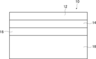
- FIG. 1 is a conceptual view showing an example of the organic EL display device of the present invention.
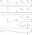
- FIG. 2 is a conceptual diagram for explaining the operation of the organic EL display device shown in FIG.
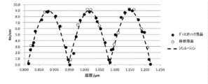
- FIG. 3 is a graph showing that the color changes periodically with respect to the film thickness of the circularly polarized light separation layer.
- FIG. 4 is a graph showing that Re changes periodically with respect to the film thickness of the circularly polarized light separation layer.
- FIG. 5 is a graph showing that a simulation result indicating that Re periodically changes with respect to the film thickness of the circularly polarized light separation layer matches an actual measurement value.
- Re ( ⁇ ) and Rth ( ⁇ ) respectively indicate in-plane retardation at the wavelength ⁇ and retardation in the thickness direction. Unless otherwise stated, the wavelength ⁇ is 550 nm.
- R0 ((lambda)) is displayed as a numerical value calculated by AxoScan, it means Re ((lambda)).
- NAR-4T Abbe refractive index
- ⁇ sodium lamp
- values of Polymer Handbook JOHN WILEY & SONS, INC
- catalogs of various optical films can be used.
- the values of the average refractive index of the main optical films are exemplified below: cellulose acylate (1.48), cycloolefin polymer (1.52), polycarbonate (1.59), polymethyl methacrylate (1.49), And polystyrene (1.59).
- visible light is light of wavelengths visible to human eyes among electromagnetic waves, and represents light in a wavelength range of 380 to 780 nm.
- Nonvisible light is light in a wavelength range of less than 380 nm or in a wavelength range of more than 780 nm.
- light in the wavelength range of 420 to 490 nm is blue light
- light in the wavelength range of 495 to 570 nm is green light
- the light is red light.
- FIG. 1 schematically shows an example of the organic electroluminescent display device of the present invention.
- the organic electroluminescent display device is also referred to as an organic EL display device.
- the organic EL display device 10 of the present invention shown in FIG. 1 has a polarizer 12, a retardation layer 14, a circularly polarized light separation layer 16, and an organic electroluminescent light emitting element 18 in this order from the viewing side.
- the organic electroluminescent light emitting device is also referred to as an organic EL light emitting device.
- the polarizer 12 and the retardation layer 14 constitute an antireflective film
- the polarizer 12, the retardation layer 14 and the circularly polarized light separating layer 16 constitute an optical laminate film of the present invention.
- the present invention can improve the luminance of display in the organic EL display device 10, can prolong the life of the organic EL element, and can also suppress the reflection of external light.
- the circularly polarized light separation layer 16 is a cholesteric liquid crystal layer.
- the cholesteric liquid crystal layer is a layer having a cholesteric liquid crystal structure formed by fixing a cholesteric liquid crystal phase.
- the cholesteric liquid crystal layer selectively reflects a specific circularly polarized component in a specific wavelength range.
- the selective reflection center wavelength of the circularly polarized light separation layer 16 is not limited, but the circularly polarized light separation layer 16 (cholesteric liquid crystal layer) preferably has a selective reflection center wavelength in the wavelength range of blue light. That is, the circularly polarized light separation layer 16 preferably reflects blue light selectively.
- the circularly polarized light separation layer 16 more preferably has a selective reflection center wavelength in the range of 430 to 480 nm.
- the circularly polarized light separation layer 16, which is a cholesteric liquid crystal layer, is substantially a C plate because the chirality of the cholesteric liquid crystal layer is averaged for light other than in the reflection region.
- light incident from an oblique direction has a so-called short wave shift (blue shift) in which the reflection range is shifted to the short wavelength side. Act as a plate.
- the organic EL light emitting element has a difference in energy required to emit light of each color, and in general, the blue light emitting element degrades faster than the green and red light emitting elements. Therefore, in consideration of the lifetime of the blue light emitting element, measures such as suppressing the light emission amount (output) of the light emitting element of each color are taken.
- the luminance of blue light can be improved, and the overall display luminance can be improved, and the length of the light emitting element of blue light that is rapidly deteriorated It is possible to extend the lifetime and to prolong the lifetime of the organic EL display device.
- a circularly polarized light separation layer 16 which is a cholesteric liquid crystal layer having a wavelength is disposed.
- the retardation layer 14 a + A plate having a positive Rth (550) value or a B plate having a positive Rth (550) value is used, and a cholesteric liquid crystal layer of the circularly polarized light separation layer 16 is More preferred is a combination using a cholesteric liquid crystal layer composed of a discotic liquid crystal compound. This is because the cholesteric liquid crystal layer made of a discotic liquid crystal compound functions as a + C plate except in the reflection region.
- the retardation layer 14 ( ⁇ / 4 film) preferably has reverse wavelength dispersion.
- a combination using a cholesteric liquid crystal layer comprising a compound is also preferred. This is because the cholesteric liquid crystal layer made of a rod-like liquid crystal compound functions as a -C plate except in the reflection region.
- the A plate, B plate and C plate will be described in detail later.
- the polarizer 12 may be a linear polarizer (linearly polarizing plate) having a transmission axis (polarization axis) of one direction and having a function of converting natural light into a specific linear polarization.
- polarizer 12 for example, various polarizers used to form an antireflection layer in various organic EL display devices can be used. Therefore, as the polarizer 12, for example, any of an iodine-based polarizing plate, a dye-based polarizing plate using a dichroic dye, and a polyene-based polarizing plate can be used.
- the iodine-based polarizing plate and the dye-based polarizing plate are generally produced by adsorbing iodine or a dichroic dye to polyvinyl alcohol and stretching.
- the polarizer 12 and the retardation layer 14 described later are arranged such that the transmission axis (absorption axis) of the polarizer 12 and the slow axis of the retardation layer 14 are 45 ° ⁇ 10 °.
- the polarizer 12 is disposed such that the direction of the transmission axis coincides with the direction of the linearly polarized light emitted from the retardation layer 14.
- the retardation layer 14 described later has a slow axis so that the direction of the linearly polarized light emitted by itself is aligned with the transmission axis of the polarizer 12 according to the direction of the circularly polarized light reflected by the circularly polarized light separating layer 16. The direction of is adjusted.
- the in-plane retardation (Re ( ⁇ )) of the retardation layer 14 in the invention is from 120 to 160 nm, preferably from 125 to 155 nm, and more preferably from 130 to 150 nm, from the viewpoint of reflection prevention. .
- the absolute value of Rth (550) which is the retardation in the thickness direction of the retardation layer 14 is 50 -200 nm is preferable, 55-180 nm is more preferable, and 60-160 nm is more preferable.
- the retardation layer 14 may be a single layer or a laminate of two or more layers.
- the retardation layer 14 is preferably a laminate of two or more layers.
- the slow axis when these layers are regarded as one layer forms 45 ° ⁇ 10 ° with the transmission axis of the polarizer 12. Good.
- the polarizer, the ⁇ / 2 plate, and the ⁇ / 4 plate are laminated in this order, it can be regarded as a laminate of the above-described polarizer and the retardation layer.
- the slow axis of the ⁇ / 2 plate is 12.5 ° ⁇ 10 °
- the slow axis of the ⁇ / 4 plate is 72.5 ° ⁇ 10 ° with respect to the transmission axis of the polarizer.
- the angle of the slow axis of the retardation layer is 45 ° ⁇ 10 ° with respect to the absorption axis of the polarizer. That is, in this case, the polarizer, the ⁇ / 2 plate, and the ⁇ / 4 plate may be combined to form a circularly polarizing plate as a whole.
- substrates such as a glass substrate and a resin film, as needed.
- the retardation layer 14 may be formed on an alignment film formed on a substrate, as necessary.
- the retardation layer 14 is preferably a ⁇ / 4 film ( ⁇ / 4 plate).
- the ⁇ / 4 film is more preferably a retardation film of one or more layers containing at least one of a liquid crystal compound formed by polymerizing a liquid crystal monomer expressing a retardation film, a nematic liquid crystal layer or a smectic liquid crystal layer.
- the retardation layer 14 is more preferably a ⁇ / 4 film formed using a polymerizable liquid crystal compound.
- the retardation film may be optically substantially uniaxial or biaxial. Examples of liquid crystal compounds include discotic liquid crystals and rod-like liquid crystal compounds.
- the retardation film it is possible to select a film stretched in the transport direction at the time of film production or stretched in the direction perpendicular to the transport direction, and a retardation film stretched 45 ° with respect to the transport direction.
- a retardation film or a transparent film on which a cyclic polyolefin resin (norbornene resin) or the like capable of producing an optical sheet member by so-called roll-to-roll can be oriented and processed Preferred is a film having on the surface a layer in which a liquid crystal compound is oriented at 45 ° with respect to the transport direction of the film at the time of production.
- a plate As used herein, the A plate is defined as follows. There are two types of A plate: positive A plate (positive A plate, + A plate) and negative A plate (negative A plate, -A plate).
- the refractive index in the slow axis direction (the direction in which the in-plane refractive index is maximum) in the film plane is nx
- the refractive index in the direction perpendicular to the in-plane slow axis and in the plane is ny
- the thickness direction When the refractive index is nz, the positive A plate satisfies the relationship of formula (A1)
- the negative A plate satisfies the relationship of formula (A2).
- the positive A plate shows a positive Rth value
- the negative A plate shows a negative Rth value.
- Formula (A1) nx> ny ⁇ nz
- Formula (A2) ny ⁇ nx ⁇ nz
- ⁇ includes not only the case where both are completely identical but also the case where both are substantially identical. “Substantially the same” means that, for example, (ny ⁇ nz) ⁇ d is included in “ny ⁇ nz” in the case of ⁇ 10 to 10 nm, preferably ⁇ 5 to 5 nm, and (nx ⁇ nz) ⁇ d However, the case of ⁇ 10 to 10 nm, preferably ⁇ 5 to 5 nm is also included in “nx5nz”. In this equation, d is the thickness of the film.
- the B plate has different values for nx, ny and nz, and satisfies the relationship of the formula (B1).
- B plate having a negative Rth and the relationship of the formula (B2); and B with a positive Rth There are two types with the plate.
- C plate There are two types of C plate: positive C plate (positive C plate, + C plate) and negative C plate (negative C plate, -C plate).
- the positive C plate satisfies the relationship of formula (C1)
- the negative C plate satisfies the relationship of formula (C2).
- the positive C plate exhibits a negative Rth value
- the negative C plate exhibits a positive Rth value.
- Formula (C1) nz> nx ⁇ ny
- Formula (C2) nz ⁇ nx ⁇ ny
- ⁇ includes not only the case where both are completely identical but also the case where both are substantially identical.
- nx ⁇ ny in the case where (nx ⁇ ny) ⁇ d is 0 to 10 nm, preferably 0 to 5 nm.
- d is the thickness of the film.
- Reverse wavelength dispersion refers to the relationship of Re (450) ⁇ Re (550) ⁇ Re (650). Specifically, the range of 0.8 to 0.9 is preferable for Re (450) / Re (550), and the range of 1.03 to 1.25 is preferable for Re (650) / Re (550). Further, with regard to the C plate described later, the C plate reverse wavelength dispersion refers to the relationship of Rth (450) ⁇ Rth (550) ⁇ Rth (650).
- the retardation layer 14 may be optically uniaxial or biaxial.
- the biaxial retardation layer 14 B plate
- the absolute value of Rth (550) is increased. Therefore, the number of turns of the cholesteric liquid crystal in the circularly polarized light separation layer 16 described later is increased to obtain blue.
- the brightness of light can be increased (the amount of blue light irradiation (the amount of blue light) can be increased).
- the biaxial retardation layer 14 is used, the reflection preventing function in the oblique direction is reduced due to the increase of the absolute value of Rth (550), and furthermore, the color balance of the display may be lost. There is also.
- the retardation layer 14 is uniaxial (A plate) in terms of the overall balance of the luminance of blue light, the anti-reflection property against oblique light, and the color balance of display. preferable.
- the circularly polarized light separation layer 16 is a cholesteric liquid crystal layer.
- the cholesteric liquid crystal layer is a layer having a cholesteric liquid crystal structure formed by fixing a cholesteric liquid crystal phase.
- the circularly polarized light separation layer 16 may be formed on a substrate such as a glass substrate and a resin film, if necessary. Furthermore, the circularly polarized light separation layer 16 may be formed on the alignment film formed on the substrate, if necessary.
- Cholesteric liquid crystal structure Cholesteric liquid crystal structures are known to exhibit selective reflectivity at specific wavelengths.
- one pitch of the helical structure in the cholesteric liquid crystal structure is the length in the thickness direction of the cholesteric liquid crystal layer when the direction of the director of the liquid crystal compound forming the cholesteric liquid crystal structure is rotated 360 °. .
- the pitch of the cholesteric liquid crystal structure depends on the type of the chiral agent to be used together with the polymerizable liquid crystal compound in the formation of the circularly polarized light separation layer 16 or the addition concentration thereof, so that the desired pitch can be obtained by adjusting these.
- For the adjustment of the pitch refer to Fujifilm Research Report No. 50 (2005) p. There is a detailed description in 60-63.
- For the method of measuring the sense and pitch of the spiral use the method described in “Introduction to Liquid Crystal Science Experiment” edited by The Liquid Crystal Society of Japan, published by Sigma Press 2007, p. it can.
- the subject of the present invention is a subject found by creating a cholesteric liquid crystal layer that selectively reflects blue light, but is a subject that occurs in the cholesteric liquid crystal layer in general, and the present invention Applicable
- the selective reflection central wavelength (central wavelength of the selective reflection wavelength region) and the half width of the circularly polarized light separation layer 16 (cholesteric liquid crystal layer) can be determined as follows.
- a drop in transmittance is observed in the selective reflection region.
- the selective reflection center wavelength and the half width can be expressed by the following equations.
- the cholesteric liquid crystal structure gives stripes of light and dark portions in a cross-sectional image perpendicular to the formation surface of the circularly polarized light separation layer 16 observed by a scanning electron microscope (SEM).
- SEM scanning electron microscope
- the two repetitions of the light part and the dark part correspond to one spiral pitch (one turn of the spiral). From this, the number of turns of the spiral of the cholesteric liquid crystal layer can be measured from the SEM cross-sectional view.
- the normal to each of the striped lines is the helical axis direction of the cholesteric liquid crystal structure.
- the cholesteric liquid crystal structure can be obtained by fixing the cholesteric liquid crystal phase.
- the structure in which the cholesteric liquid crystal phase is fixed may be a structure in which the orientation of the liquid crystal compound in the cholesteric liquid crystal phase is maintained, and typically, the polymerizable liquid crystal compound is in the aligned state of the cholesteric liquid crystal phase. It is sufficient if it has a structure in which it is polymerized and cured by ultraviolet irradiation, heating or the like to form a layer having no fluidity, and at the same time, it changes into a state in which no change occurs in the alignment form by external field or external force.
- the liquid crystal compound may no longer exhibit liquid crystallinity.
- the polymerizable liquid crystal compound may become high in molecular weight by the curing reaction and may no longer have liquid crystallinity.
- the liquid-crystal composition containing a liquid crystal compound etc. are mentioned.
- the liquid crystal compound is preferably a polymerizable liquid crystal compound.
- the liquid crystal composition containing the polymerizable liquid crystal compound further contains a surfactant, a chiral agent (chiral agent), a polymerization initiator and the like.
- a surfactant a chiral agent (chiral agent), a polymerization initiator and the like.
- examples of the surfactant, the chiral agent, and the polymerization initiator include compounds described in JP-A-2016-197219.
- the polymerizable liquid crystal compound may be a rod-like liquid crystal compound or a discotic liquid crystal compound.
- the retardation layer 14 is preferably reverse wavelength dispersive, and when the reverse wavelength dispersive retardation layer 14 is used, it is between the polarizer 12 and the organic EL light emitting element 18 described later.
- a discotic liquid crystal compound is suitably used in that the total retardation Rth (550) of the members disposed in the thickness direction can be suitably made.
- the polymerizable group include acryloyl group, methacryloyl group, epoxy group, and vinyl group.
- disc-like liquid crystal compound examples include those described in JP-A-2007-108732, JP-A-2010-244038, JP-A-2013-195630, JP-A-10-307208, and JP-A-2000-171637.
- JP-A-2013-195630 describes that the discotic liquid crystal compound is preferably a compound having a triphenylene structure.
- a discotic liquid crystal compound having a trisubstituted benzene structure can have a higher ⁇ n and a wider selective reflection wavelength range than a triphenylene structure, and therefore can be appropriately selected as necessary.
- Rod-like liquid crystal compounds include azomethines, azoxys, cyanobiphenyls, cyanophenyl esters, benzoic acid esters, cyclohexanecarboxylic acid phenyl esters, cyanophenylcyclohexanes, cyano substituted phenyl pyrimidines, alkoxy substituted phenyl pyrimidines, Phenyldioxanes, tolanes and alkenylcyclohexyl benzonitriles are preferably used.
- rod-like liquid crystal compounds which are polymerizable liquid crystal compounds
- Examples of rod-like liquid crystal compounds which are polymerizable liquid crystal compounds include Makromol. Chem. 190, 2255 (1989), Advanced Materials 5: 107 (1993), U.S. Pat. Nos. 4,683,327, 5,622,648, 5,77,0107, WO 95/22586, 95 / 24,455, 97 /
- the compounds described in, for example can be used.
- the rod-like liquid crystal compound for example, the compounds described in JP-A-11-513019 or JP-A-2007-279688 can be preferably used.
- the reflectance of blue light is influenced by the number of turns of the spiral. Specifically, the reflectance of blue light can be increased and the brightness of blue light can be increased as the number of turns of the spiral of the cholesteric liquid crystal layer is increased.
- the absolute value of Rth (550) of the circularly polarized light separation layer 16 increases as the number of turns of the spiral increases.
- the sum of Rth (550) of members provided between the polarizer 12 and the organic EL light emitting element 18 is preferably ⁇ 50 to 50 nm. Therefore, the number of turns of the spiral in the circularly polarized light separation layer 16 depends on the required luminance of blue light, Rth (550) of the member provided between the polarizer 12 and the organic EL light emitting element 18, etc. It may be set as appropriate.
- the number of turns of the helix of the cholesteric liquid crystal layer is 1.5 to 6.5 pitch ( 1.5 to 6.5 times) is preferred. Control of the number of turns of the spiral is possible by controlling the film thickness of the circularly polarized light separation layer 16.
- the film thickness of the circularly polarized light separation layer 16 is preferably 0.4 to 1.8 ⁇ m, and more preferably 0.8 to 1.3 ⁇ m.
- the circularly polarized light separation layer 16 which is a cholesteric liquid crystal layer generates Re (550) in the plane.
- ReMAX [nm] corresponding to the maximum value of Re (550) of the circularly polarized light separation layer periodically changing with the film thickness change is defined by the following equation.
- n the average refractive index of the liquid crystal compound forming the circularly polarized light separation layer 16
- ⁇ n the birefringence of the liquid crystal compound forming the circularly polarized light separation layer
- ⁇ the selective reflection center wavelength of the circularly polarized light separation layer 16 Respectively.
- Re (550) of the circularly polarized light separation layer 16 is “0.5 ⁇ ReMax ⁇ Re (550) ⁇ ReMax” Meet.
- the present invention provides an optical laminated film excellent in uniformity of reflected color even with a large size (large area) by having such a configuration, and a reflected color at the time of quenching even with a large area.
- An organic EL display device excellent in uniformity of taste is realized.
- the present inventors repeated studies to improve the quality of a configuration in which a circularly polarized light separation layer is provided to improve luminance in an organic EL display device using an antireflection film consisting of a polarizer and a retardation layer. The As a result, it was found that when viewed from the front when the organic EL display was quenched, the reflected color was not uniform and unevenness occurred. Furthermore, it has been found that this change in color is due to the change in Re (550) of the circularly polarized light separation layer 16 periodically changing corresponding to the film thickness of the circularly polarized light separation layer.
- the film thickness of the circularly polarized light separation layer (cholesteric liquid crystal layer) in the organic EL display device having the polarizer, the retardation layer, the circularly polarized light separation layer, and the organic EL light emitting device in this order in FIG. An example of a relationship with chromaticity a * at the time of observation is shown. The details of FIG. 3 will be described later in an example. As shown in FIG.
- FIG. 4 shows an example of the relationship between the film thickness and Re (550) of the circularly polarized light separation layer in the circularly polarized light separation layer (cholesteric liquid crystal layer) constituting the organic EL display of FIG. The details of FIG.
- Re (550) of the circularly polarized light separation layer also gradually increases with the increase or decrease of the film thickness, and gradually decreases with the certain thickness as the apex, and the certain thickness as the lowest point. As it becomes, again, it becomes cyclically repeated according to film thickness that becomes large gradually.
- the thickness of the circularly polarized light separation layer at which the color value is the maximum value and the thickness of the circularly polarized light separation layer at which the Re (550) is the maximum value coincide with each other.
- the thickness of the circularly polarized light separation layer at which the color tone is minimized and the thickness of the circularly polarized light separation layer at which Re (550) is minimized are the same. That is, changes in color and Re (550) with respect to the thickness of the circularly polarized light separation layer are repeated in the same cycle according to changes in the film thickness. This is due to the orientation of the slow axis (director) of the liquid crystal compound located on the outermost surface of the circularly polarized light separation layer.
- the outermost surface of the circularly polarized light separation layer is the surface of the circularly polarized light separation layer on the side opposite to the coated surface on which the liquid crystal composition to be the circularly polarized light separation layer is applied.
- the liquid crystal compound is spirally swirled.
- Re (550) becomes zero when the liquid crystal compound is rotated 360 ° on the outermost surface. That is, in the circularly polarized light separating layer, in the cholesteric liquid crystal structure which turns in a spiral, if the direction of the slow axis of the liquid crystal compound on the lowermost surface matches the direction of the slow axis of the liquid crystal compound on the outermost surface, Re (550) becomes zero.
- the thickness of the circularly polarized light separation layer is a thickness in a state where the liquid crystal compound is rotated 360 °.
- the film thickness of the circularly polarized light separation layer is increased from the state where the liquid crystal compound is rotated 360 °, the liquid crystal compound which turns in a spiral shape is placed thereon.
- the circularly polarized light separation layer becomes thinner.
- the direction of the slow axis of the liquid crystal compound on the outermost surface of the circularly polarized light separation layer deviates from the state rotated 360 °.
- the deviation of the slow axis of the liquid crystal compound from the 360 ° rotated state causes optical anisotropy to occur in the plane of the circularly polarized light separation layer.
- the larger the deviation of the slow axis of the liquid crystal compound from the 360 ° rotated state the larger the optical anisotropy in the plane of the circularly polarized light separation layer, and the larger the Re (550). That is, in the circularly polarized light separation layer, Re (550) is maximized when the direction of the slow axis of the liquid crystal compound on the outermost surface is rotated by 90 ° from the state rotated by 360 °. For example, in the example shown in FIG. 4, Re (550) of about 9 nm is generated at the maximum.
- Re (550) of the circularly polarized light separation layer generated in this manner that is, the phase difference, It affects the combined optical performance, and causes uneven color at the time of extinction.
- the change in Re (550) corresponding to the change in thickness of the circularly polarized light separation layer is This corresponds to the color unevenness at the time of quenching to be improved, ie, the color non-uniformity at the time of quenching.
- This problem is noticeable in large image display devices, particularly large image display devices of 50 inches or more, particularly organic EL display devices.
- Re (550) that is, the color of the circularly polarized light separation layer varies with the thickness of the circularly polarized light separation layer.
- the circularly polarized light separation layer is formed by a coating method. Therefore, in the case of a circularly polarized light separation layer of a small size, the film thickness difference across the entire surface is small, and the color uniformity across the entire surface can be easily ensured.
- a large size (large area) optical laminated film it is difficult to make the film thickness of the circularly polarized light separation layer uniform, and the film thickness of the circularly polarized light separation layer is gentle and large. Distribution will occur. As a result, when the entire surface of the image display apparatus at the time of extinction is viewed, for example, a large difference in tint occurs between the center and the ends, between the ends, and the like.
- a large image display device is far from the observation distance, and although small color unevenness at the time of extinction is inconspicuous, color unevenness such as a large unery at the time of extinction is very noticeable. Will be a major cause of quality degradation,
- the inventors conducted a simulation based on the above-described consideration, with the horizontal axis representing the film thickness of the circularly polarized light separation layer (helical pitch) and the vertical axis representing Re (550). As a result, as shown by a broken line in FIG. 5, it was almost in agreement with the measurement result shown in FIG.
- the region centered on the film thickness corresponding to 0.5 ⁇ N + 0.25 pitch (N is a natural number) is a stable region where the change of Re (550) with respect to the film thickness change of the circularly polarized light separation layer is small.
- N is a natural number
- the center value of the film thickness is 0.5 ⁇ N + 0.25 pitch (N is a natural number
- the present inventors conceived of utilizing the stable region where the change in Re (550) with respect to the change in film thickness of the circularly polarized light separation layer 16 is small, and reached the present invention. That is, according to the present invention, an optical laminated film having a polarizer 12, a retardation layer 14 and a circularly polarized light separation layer 16 in this order, and a polarizer 12, a retardation layer 14, a circularly polarized light separation layer 16 and an organic EL light emission In the organic EL display device 10 having the elements 18 in this order, Re (550) of the circularly polarized light separation layer 16 satisfies the following formula (1), and preferably satisfies the formula (2).
- ReMax represents the maximum value of Re (550) that changes periodically in response to changes in the thickness of the circularly polarized light separation layer 16.
- ReMax is proportional to the birefringence ⁇ n of the liquid crystal compound used to form the circularly polarized light separation layer 16 and the helical pitch film thickness of the circularly polarized light separation layer 16.
- the helical pitch film thickness is a film thickness of one helical pitch in which the slow axis (director) of the liquid crystal compound is rotated 360 ° in the above-described cholesteric liquid crystal structure.
- the helical pitch film thickness of the circularly polarized light separation layer 16 is ⁇ of the selective reflection center wavelength of the polarized light separation layer 16 (cholesteric liquid crystal layer), and n is the average refractive index of the liquid crystal compound forming the circularly polarized light separation layer 16 Then, it is represented by “ ⁇ / n”.
- k is a proportionality constant calculated
- the present invention suppresses the change of Re (550), that is, the change of color with respect to the change of the film thickness of the circularly polarized light separation layer 16 by having such a configuration, and an optical laminated film having high uniformity of reflected color.
- an organic EL display device with high uniformity of reflected color at the time of extinction is realized.
- the present invention utilizes the large Re (550) region of the circularly polarized light separation layer 16 and is disadvantageous in terms of the deviation of the reflected color from the design value (intended color) at the time of extinction. It is.
- the overall color unevenness has a greater adverse effect on the quality than the deviation of the reflected color from the design value.
- the effect of improving the quality by eliminating the unevenness of the overall reflection color and improving the uniformity is very large.
- the larger the ⁇ n the smaller the film thickness of the circularly polarized light separation layer 16 is, and it is preferable to use a liquid crystal compound with a ⁇ n of 0.1 to 0.2.
- ReMax is 6 to 12 nm. Become. If the selective reflection center wavelength of the circularly polarized light separation layer 16 is increased, the helical pitch film thickness of the circularly polarized light separation layer 16 also increases in proportion, but the film thickness period in which Re (550) changes is also proportionally large. Therefore, the rate of change of Re (550) with respect to the change of the film thickness of the circularly polarized light separation layer 16 depends on ⁇ n.
- Re (550) of the circularly polarized light separation layer 16 is less than “0.5 ⁇ ReMax”, Re (550), ie, the change in tint with respect to the change in film thickness of the circularly polarized light separation layer 16 is large, and the reflective color uniformity is uniform. It is not possible to obtain an optical laminated film having high properties and an organic EL display device having high uniformity of reflected color at the time of quenching. On the other hand, it is basically impossible that Re (550) of the circularly polarized light separation layer 16 exceeds “ReMax”, and at this time, it is considered that some trouble has occurred.
- Re (550) of the circularly polarized light separation layer 16 preferably satisfies “0.7 ⁇ ReMax ⁇ Re ⁇ ReMax”, and “0.8 ⁇ ReMax ⁇ Re ⁇ ReMax”. It is more preferable to fill.
- Re (550) of the circularly polarized light separation layer 16 is 5 ⁇ obtained by dividing the display surface (optical laminated film) of the organic EL display device 10 into five equal parts by the short side and five equal parts by the long side.
- the optical laminated film and the organic EL display device 10 of the present invention preferably correspond to a large size (large screen).
- the organic EL display device 10 of the present invention is preferably 50 inches or more, more preferably 55 inches or more, and still more preferably 65 inches or more. That is, it is preferable that the optical laminated film of the present invention has a size corresponding to an image display apparatus of these sizes.
- Re (550) is generated in the plane of the circularly polarized light separation layer 16. That is, the circularly polarized light separation layer 16 has a phase difference in the plane. Therefore, the circularly polarized light separation layer 16 has a slow axis in the plane.
- the change in color of the organic EL display at the time of extinction which is caused by the generation of Re (550) by the circularly polarized light separation layer, is caused by the slow axis of the circularly polarized light separation layer 16 and the slow axis of the retardation layer 14
- the angle formed by the dots is largely different.
- the influence of the difference in tint can be suppressed.
- the influence of tint difference can be further suppressed by setting the angle formed by the slow axis of the circularly polarized light separation layer 16 and the slow axis of the retardation layer 14 to -25 ° to 25 °.
- the angle formed by the slow axis of the circularly polarized light separation layer 16 and the slow axis of the retardation layer 14 is preferably -20 ° to 20 °, and more preferably -10 ° to 10 °.
- the angle between the slow axis of the circularly polarized light separation layer 16 and the slow axis of the retardation layer 14 is an optical laminated film in which the polarizer 12, the retardation layer 14 and the circularly polarized light separation layer 16 are laminated.
- the state in which the slow axis of the circularly polarized light separation layer 16 is clockwise with respect to the slow axis of the phase difference layer 14 is shown as a positive value.
- a difference in film thickness occurs within the plane of the circularly polarized light separation layer 16, and the slow axis of the liquid crystal compound of the circularly polarized light separation layer 16. There are variations in the direction.
- the display surface (optical laminated film) of the organic EL display device 10 is equally divided into 25 areas of 5 ⁇ 5, which are equally divided into five by the short side and five by the long side.
- the angle between the slow axis of the circularly polarized light separation layer 16 and the slow axis of the retardation layer 14 is measured at the central portion of the film, and the slow axis of the circularly polarized light separation layer 16 and the slow axis of the retardation layer 14 are The average of the maximum value and the minimum value of the angles formed is the angle formed by the slow axis of the circularly polarized light separation layer 16 and the slow axis of the retardation layer 14.
- the slow axis of the circularly polarized light separation layer 16 or the cholesteric liquid crystal layer can be measured by the above-mentioned AxoScan.
- the circularly polarized light separation layer 16 has the selective reflection central wavelength in the wavelength range of blue light, preferably in the wavelength range of 430 to 480 nm, but the present invention is not limited thereto. That is, the selective reflection center wavelength of the circularly polarized light separation layer 16 (cholesteric liquid crystal layer) is, for example, according to the color to be improved in luminance in the organic EL display device and the color to suppress generation of tint when observed obliquely.
- Various wavelength bands of light are available, such as UV, green, red and infrared.
- a circularly polarized light separating layer 16 having a selective reflection center wavelength in the wavelength range of 700 to 800 nm is exemplified.
- the sum (sum) of Rth (550) of members provided between the polarizer 12 and the organic EL light emitting element 18 is ⁇ 50 to 50 nm ( ⁇ 50 nm). preferable.
- the absolute value of the sum of Rth (550) of members provided between the polarizer 12 and the organic EL light emitting device 18 is preferably 50 nm or less.
- the sum of Rth (550) of members provided between the polarizer 12 and the organic EL light emitting device 18 is more preferably ⁇ 40 to 40 nm, and further ⁇ 20 to 20 nm Preferably, -10 to 10 nm is particularly preferred.
- the Rth (550) of a member provided between the polarizer 12 and the organic EL light emitting element 18 -20 to 20 nm is preferable, and -10 to 10 nm is more preferable.
- the sum of Rth (550) of the retardation layer 14 and Rth (550) of the circularly polarized light separation layer 16 be ⁇ 50 to 50 nm. .
- the reverse wavelength dispersive + A plate or Rth (550) having a positive value of Rth (550) is used.
- a circularly polarized light separation layer 16 (cholesteric) composed of a reverse wavelength dispersive B plate which is a positive value and a discotic liquid crystal compound which functions substantially as a + C plate in the visible light region and which has a negative Rth (550) A combination of the liquid crystal layer) is exemplified.
- a forward dispersive -A plate or Rth (550) in which Rth (550) is a negative value a forward dispersive -A plate or Rth (550) in which Rth (550) is a negative value.
- Circularly polarized light separation layer 16 composed of a rod-like liquid crystal compound having a positive value of Rth (550), which functions substantially as a -C plate in the visible light region, And a combination of a cholesteric liquid crystal layer).
- the total of Rth (550) of members provided between the polarizer 12 and the organic EL light emitting element 18 is ⁇ 50 to 50 nm, and the reflection preventing function, particularly the reflection preventing function in the oblique direction
- a C plate may be added between the polarizer 12 and the organic EL light emitting device 18 as needed.
- the reflectance of blue light can be increased and the brightness of blue light can be increased as the number of turns of the spiral of the cholesteric liquid crystal layer increases.
- the number of turns of the spiral of the circularly polarized light separation layer 16 increases (for example, when the number of turns of the spiral is 6 or more)
- the absolute value of Rth (550) of the circularly polarized light separation layer 16 increases, and the retardation layer
- Rt cholesteric liquid crystal layer
- a ⁇ C plate having a positive value 550) is provided between the polarizer 12 and the organic EL light emitting element 18.
- the phase difference layer 14 is composed of a normal dispersion -A plate in which Rth (550) is a negative value or a forward dispersion B plate in which Rth (550) is a negative value,
- Rth (550) is a negative value
- the circularly polarized light separating layer 16 made of a rod-like liquid crystal compound having a positive value of Rth (550) which substantially functions as a -C plate in the light region
- the Rth (550) has a negative value.
- a certain + C plate is provided between the polarizer 12 and the organic EL light emitting element 18.
- the organic EL display device of the present invention there are no problems in the thickness of the organic EL display device, the complexity of the layer configuration between the polarizer 12 and the organic EL light emitting element 18, cost and productivity.
- a configuration having a C plate between the polarizer 12 and the organic EL light emitting element 18 is most advantageous.
- the organic EL display device 10 shown in FIG. Like the above, a configuration having only the retardation layer 14 and the circularly polarized light separation layer 16 between the polarizer 12 and the organic EL light emitting element 18 is advantageous.
- All known C plates can be used.
- a commercially available optical film may be used as a C plate.
- the arrangement position of the C plate is preferably between the retardation layer 14 and the circularly polarized light separation layer 16 or between the circularly polarized light separation layer 16 and the organic EL light emitting element 18.
- the Rth (550) of the C plate is not limited, but in order not to cause tinting due to retardation, the absolute value of Rth (550) of the C plate is preferably 300 nm or less.
- the C plate a plurality of the same C plate or different C plates may be used in combination, as necessary.
- the organic EL light emitting element 18 displays an image by the organic EL.
- the organic EL light emitting element 18 includes a transparent electrode layer (TFT (Thin Film Transistor), thin film transistor), a hole injection layer, a hole transport layer, an organic EL light emitting layer, a hole blocking layer, an electron transport layer, an electron injection layer, and, it is a known organic EL light emitting element that constitutes an organic EL light emitting device (OLED) such as an organic EL display and an organic EL lighting device having a cathode or the like.
- OLED organic EL light emitting device
- the organic EL light emitting element 18 one obtained by removing the antireflection layer (antireflection film) from a known organic EL display, an organic EL display without an antireflection layer, a known organic EL display, etc. It is available.
- FIG. 2 conceptually shows the organic EL display device 10 of the present invention shown in FIG. 1 and the conventional organic EL display device 100 disassembled.
- the conventional organic EL display device 100 also usually has a combination of a polarizer 12 and a retardation layer 14 ( ⁇ / 4 plate) as an antireflection film.
- the blue light b emitted by the organic EL light emitting element 18 first enters and transmits the retardation layer 14, and then enters the polarizer 12.
- the length of the arrow of blue light b represents light intensity (light quantity). Since the polarizer 12 transmits only linear polarized light in a predetermined direction (referred to as the x direction), linearly polarized light in the direction orthogonal to the x direction is blocked by the polarizer 12. Therefore, the blue light b transmitted through the polarizer 12 is only a half linearly polarized light bx of blue in the x direction.
- the blue light b emitted by the organic EL light emitting element 18 first enters the circularly polarized light separation layer 16.
- the circularly polarized light separation layer 16 cholesteric liquid crystal layer
- blue left circularly polarized light bL is transmitted and blue right circularly polarized light bR is reflected.
- Ru The blue left circularly polarized light bL transmitted through the circularly polarized light separating layer 16 is then incident on the retardation layer 14 ( ⁇ / 4 plate) and transmitted to be blue linearly polarized light bx in the x direction.
- the linearly polarized blue light bx then enters the polarizer 12.
- the polarizer 12 transmits only linearly polarized light in the x direction. Accordingly, blue linearly polarized light bx which is linearly polarized light in the x direction is transmitted through the polarizer 12 and emitted.
- the blue right circularly polarized light bR reflected by the circularly polarized light separation layer 16 is incident on the organic EL light emitting element 18 (substrate of the light emitting element) and reflected, and the turning direction of the circularly polarized light is reversed. It becomes circularly polarized light bL.
- the blue left circularly polarized light bL reflected by the organic EL light emitting element 18 is then incident on the circularly polarized light separation layer 16, but as described above, only the blue right circularly polarized light bR is reflected, so the blue left circle The polarized light bL passes through the circularly polarized light separation layer 16.
- the left circularly polarized light bL of blue is then converted by the retardation layer 14 into linearly polarized light bx of blue, which is linearly polarized light in the x direction, and then transmits only linearly polarized light in the x direction The light is transmitted through the polarizer 12 and emitted.
- the circularly polarized light is separated so that the direction of the linearly polarized light emitted from the retardation layer 14 coincides with the direction of the transmission axis of the polarizer 12.
- the direction of the circularly polarized light reflected by the layer 16, the slow axis of the retardation layer 14, and the transmission axis of the polarizer 12 it is possible to emit about twice as much blue light as the conventional organic EL display .
- the brightness of blue light can be approximately doubled as compared with the prior art, so by improving the brightness of red light and green light in accordance with blue light A bright image can be displayed.
- the display brightness may be the same as that of the conventional organic EL display device, the output of the blue light source (organic EL light source emitting blue light) can be reduced. It is possible to realize the organic EL display device 10 with high quality. Such an effect is that, even if the circularly polarized light separation layer 16 has the selective reflection center wavelength in the red light wavelength region, the circularly polarized light separation layer 16 selectively reflects the green light wavelength region in accordance with the corresponding light color. Even if it has a wavelength, it can be obtained similarly.
- TAC film triacetyl cellulose film manufactured by Fujifilm Corporation was prepared.
- the following alignment film coating solution was prepared, heated and dissolved at 85 ° C. for 1 hour while stirring, and filtered through a 0.45 ⁇ m filter.
- the prepared alignment film coating solution was coated on a TAC film while adjusting the coating amount so that the film thickness after drying was 0.5 ⁇ m, and dried at 100 ° C. for 2 minutes.
- the dried coating film was subjected to rubbing treatment to prepare a film-like temporary support.
- the direction of rubbing was parallel to the longitudinal direction of the film.
- a common polyethylene terephthalate film PET film, for example, Cosmo Shine A4100 manufactured by Toyobo Co., Ltd.
- PET film for example, Cosmo Shine A4100 manufactured by Toyobo Co., Ltd.
- Coating solution A for a circularly polarized light separation layer having the following composition was prepared, dissolved by heating at 25 ° C. for 1 hour, and filtered with a 0.45 ⁇ m filter.
- Disk-like liquid crystal compound (compound 101) 80 parts by weight Disk-like liquid crystal compound (compound 102) 20 parts by weight Additive 1 1.8 parts by weight Additive 2 0.16 parts by weight Additive 3 (manufactured by DIC Corporation) F444) 0.5 parts by weight Photopolymerization initiator 1 3 parts by weight Chiral agent 1 5.18 parts by weight Methyl ethyl ketone 400 parts by weight Cyclohexanone 50 parts by weight---------------- ⁇
- the prepared coating solution A for a circularly polarized light separation layer was applied (coating width 1200 mm) to the rubbing-treated surface of the temporary support using Giesser. Subsequently, the coated film was dried at 100 ° C. for 2 minutes to evaporate the solvent, and then heat aging was performed at 115 ° C. for 3 minutes to obtain a uniform alignment state. Thereafter, the coated film is maintained at 45 ° C. and irradiated with ultraviolet light (300 mJ / cm 2 ) using a high pressure mercury lamp in a nitrogen atmosphere to reflect blue right circularly polarized light (circularly cholesteric liquid crystal layer) A formed.
- the formed circularly polarized light separating layer A was cut into slits with an application width of 10 mm.
- a sample with a substantially uniform film thickness (within ⁇ 5 nm) was obtained.
- the central slit was selected, and the cross section of the circularly polarized light separation layer A was observed by SEM.
- the film thickness of the central slit was 1.08 ⁇ m, and the number of turns of the spiral was 4.0 pitch. That is, the period of one pitch is 0.27 ⁇ m.
- a glass substrate having an adhesive layer formed on one side was prepared.
- the produced circularly polarized light separation layer A side was bonded to the pressure-sensitive adhesive layer side of this glass substrate, and the temporary support was peeled off.
- the period of one pitch was calculated from (selective reflection center wavelength) / (average refractive index) to be 0.27 ⁇ m, which was confirmed to be consistent with the above-described SEM observation. From this, it was confirmed that the circularly polarized light separating layer A reflects blue light and is a + C plate except for the selective reflection area.
- a coating solution B for a circularly polarized light separation layer having the following composition was prepared.
- ⁇ ⁇ ⁇ Coating solution B for circularly polarized light separation layer ⁇ 100.0 parts by mass of a mixture of rod-like liquid crystal compounds described below 3.0 parts by mass of a photopolymerization initiator 1 6.6 parts by mass of a chiral agent 2 0.095 parts by mass of an additive 4 Additive 3 (manufactured by DIC Corporation) , F 444) 0.5 parts by weight ⁇ methyl ethyl ketone 400 parts by weight ⁇ cyclohexanone 50.0 parts by weight ⁇ ⁇
- the prepared coating solution B for a circularly polarized light separation layer was applied (coating width 1200 mm) to the rubbing-treated surface of the temporary support using Giesser. Subsequently, the coated film is dried at 95 ° C. for 1 minute, and then irradiated with ultraviolet light (500 mJ / cm 2 ) at 25 ° C. using a high pressure mercury lamp to reflect blue right circularly polarized light Layer) B was formed. The formed circularly polarized light separation layer B was cut into slits at an application width of 10 mm.
- a glass substrate having an adhesive layer formed on one side was prepared.
- the formed circularly polarized light separation layer B side was bonded to the adhesive layer side of this glass substrate, and the temporary support was peeled off.
- Re (550) / Rth (550) 0.7 nm / 77 nm.
- the wavelength (selective reflection center wavelength) at which the transmittance for light from the normal direction is minimum was 454 nm, and the transmittance was 35%.
- the period of one pitch was calculated from (selective reflection center wavelength) / (average refractive index) to be 0.27 ⁇ m, which was confirmed to be consistent with the above-described SEM observation. Thereby, it was confirmed that the circularly polarized light separation layer B reflected blue light and became a -C plate except for the selective reflection area.
- the coating liquid for retardation layers of the following composition was prepared.
- a PET film (75 ⁇ m in thickness, manufactured by Fujifilm Corp.) whose one side was rubbed was prepared.
- the rubbing direction was 45 ° to the longitudinal direction of the PET film.
- the prepared coating solution for retardation layer was applied to the rubbing-treated surface of the temporary support.
- the coated film was dried at 90 ° C. for 2 minutes, and after evaporating the solvent, it was heat aged at 60 ° C. for 3 minutes to obtain a uniform orientation state. Thereafter, the coated film is maintained at 60 ° C. and irradiated with ultraviolet light (500 mJ / cm 2 ) using a high pressure mercury lamp under a nitrogen atmosphere to form a retardation layer (optically anisotropic layer) having a thickness of 2.0 ⁇ m. It formed.
- ultraviolet light 500 mJ / cm 2
- a glass substrate having an adhesive layer formed on one side was prepared.
- the formed retardation layer was bonded to the pressure-sensitive adhesive layer side of this glass substrate to peel off the temporary support.
- the retardation of the retardation layer was measured by AxoScan and the following values were obtained.
- the measurement wavelengths were 450 nm, 550 nm and 650 nm.
- the above table shows that Re and Rth at wavelength 450 nm are 119 nm and 60 nm, respectively, and Re and Rth at wavelength 550 nm are 140 nm and 70 nm, respectively, and Re and Rth at wavelength 650 nm are 147 nm and 74 nm, respectively.
- the retardation layer was a ⁇ / 4 film of + A plate having reverse wavelength dispersion.
- the retardation layer is also referred to as a ⁇ / 4 film.
- TAC film (Fuji Film, Fujitac TD80UL) is immersed in a 1.5 N aqueous solution of sodium hydroxide at 55 ° C. for 2 minutes, washed in a water bath at room temperature, and 0.1 N sulfuric acid at 30 ° C. Used to neutralize. The neutralized TAC film was again washed in a washing bath at room temperature and further dried with hot air at 100.degree.
- a roll was prepared by winding a polyvinyl alcohol film (PVA film) having a thickness of 80 ⁇ m.
- the PVA film was drawn out from the roll, continuously stretched 5 times in the longitudinal direction in an aqueous iodine solution, and dried to obtain a polarizer with a thickness of 20 ⁇ m.
- a TAC film was bonded to only one side of the polarizer to prepare a one-sided polarizer.
- the degree of polarization was 99.97%
- the single plate transmittance was 43%.
- the degree of polarization and the single plate transmittance were measured using a spectrophotometer (VAP-7070, manufactured by JASCO Corporation).
- a ⁇ / 4 film was laminated on the polarizer side of the one-sided polarizer such that the slow axis made an angle of 45 ° ⁇ 10 ° with the transmission axis of the polarizer. Furthermore, on the side on which the ⁇ / 4 film is laminated, the circularly polarized light separation layer A is laminated so that the surface of the circularly polarized light separation layer A faces the ⁇ / 4 film, and after lamination, temporary support of the ⁇ / 4 film The body was peeled off to produce a laminated film.
- an angle formed by the rubbing direction of the alignment film when forming the circularly polarized light separation layer A and the slow axis of the ⁇ / 4 film was set to 45 ° ⁇ 10 °.
- a laminated film was similarly produced for the circularly polarized light separation layer B.
- bonding of each layer was performed using the adhesive (SOKEN CHEMICAL Co., Ltd. make, SK2057).
- This adhesive is a substance without refractive index anisotropy, and thus Rth is 0 nm.
- the chromaticity a * when viewed from the front at the time of extinction is measured, and as shown in FIG. 3, the relationship between the film thickness of the circularly polarized light separation layer and the chromaticity a * is I made a graph.
- the circularly polarized light separation layer B various circularly polarized light separation layers having different film thicknesses are formed, and similarly, a laminated film is produced, and an organic EL display device is produced.
- the relationship between the film thickness and the chromaticity a * was detected and is also shown in the graph of FIG. In FIG.
- the black circle (separation layer A) corresponds to the circularly polarized light separation layer A, and is an organic EL display device using a circularly polarized light separation layer formed of a discotic liquid crystal compound, and white circle (separation layer B).
- the chromaticity was measured using a spectrocolorimeter (CM-2022 manufactured by Konica Minolta) under the conditions of D65, viewing angle of 10 °, and SCI. As shown in FIG.
- the change in chromaticity when viewed from the front occurs corresponding to the change in film thickness of the circularly polarized light separation layer, and periodically according to the film thickness. It has been confirmed that this period substantially matches 0.135 .mu.m, which is half of the helical pitch of the circularly polarized light separation layer.
- the relationship between the film thickness of the circularly polarized light separation layer and Re (550) is I made a graph.
- Re (550) of the circularly polarized light separation layer periodically changes in accordance with the film thickness of the circularly polarized light separation layer, and the periodical change coincides with the change in tint with respect to the film thickness.
- the black circles (separation layer A) are circularly polarized light separation layers formed of a discotic liquid crystal compound corresponding to the circularly polarized light separation layer A
- the white circles (separation layers B) are circularly polarized light. It is a circularly polarized light separation layer formed of a rod-like liquid crystal compound corresponding to the separation layer B.
- ReMAX of the circularly polarized light separation layer A was 9.0 nm
- ReMAX of the circularly polarized light separation layer B was 9.2 nm.
- Re (550) is shifted by about 9 nm at maximum, and a large color difference is generated. That is, in the large-area organic EL display device, it was clearly shown that the problem is to reduce the deviation of Re (550) in order to ensure the uniformity of the reflected color at the time of extinction.
- N is a natural number, preferably 6 to 15.
- the change of macro Re (550) in the circularly polarized light separation layer is correlated with the direction of the director of the liquid crystal compound on the outermost surface of the circularly polarized light separation layer, and the color is uniform 40 mm ⁇ 40 mm From the sample (Re (550) 7.1 nm, axis angle 64 °), nine points were selected at equal intervals, and the direction of the director of the liquid crystal compound was measured by sum frequency generation spectroscopy (SFG spectroscopy).
- FSG spectroscopy sum frequency generation spectroscopy
- the director orientations of the liquid crystal compounds are various (0 °, 38 °, 28 °, 28 °, 40 °, 32 °, 22 °, 39 °, 25 ° and 40 ° with respect to the rubbing direction) At least microscopic orientations of the director were not matched.
- the circularly polarized light separation layers of Samples A1 to A10 are circularly polarized light separation layers using a discotic liquid crystal compound (DLC), and the circularly polarized light separation layers of Samples B1 to B3 are rod-like liquid crystal compounds (CLC) It is a circularly polarized light separation layer.
- the direction of the slow axis) and the selective reflection center wavelength were measured.
- the thickness of the circularly polarized light separation layer, Re (550) and the selective reflection center wavelength were measured as described above.
- the angle of the slow axis is the average value of the maximum value and the minimum value of the angle in the 25 regions of the circularly polarized light separation layer, and the slow axis of the ⁇ / 4 film (retardation layer) and the circularly polarized light separation layer. It was an angle ⁇ formed by the slow axis. Further, Re (550) was finely adjusted with the film thickness of the ⁇ / 4 film so that the color tone in the region of the average film thickness of each sample of the circularly polarized light separation layer became black with respect to the ⁇ / 4 film. The organic EL display was produced as mentioned above using the produced lamination film.
- C In 25 regions of the organic EL display device, there are one or more regions where the chromaticity difference ⁇ E * ab with the other regions is 1.0 or more, but all 25 regions are the other 24 regions And the chromaticity difference ⁇ E * ab is less than 2.0 In this case, since the color difference in the 25 area of the organic EL display device was not noticeable visually, it is within the allowable range.
- D In 25 areas of the organic EL display device, there is at least one area in which the chromaticity difference ⁇ E * ab from other areas is 2.0 or more. In this case, the color difference is noticeable in the 25 area of the organic EL display device when viewed visually, which is not acceptable.
- a color difference is not visually recognized at all in the 25 area of the organic EL display device.
- B The color difference can not be understood unless you look at the area 25 of the organic EL display.
- C Because the color difference is not noticeable in 25 areas of the organic EL display, it is within the allowable range.
- D The color difference is noticeable in 25 areas of the organic EL display device and is not acceptable.
- the maximum light quantity in the wavelength range of 430 to 480 nm when the organic EL display was blue was measured from the normal direction of the organic EL display (blue light quantity).
- the maximum light quantity in the wavelength range of 700 to 800 nm when the organic EL display was in red was measured from the normal direction of the organic EL display (red light quantity).
- the evaluation was performed using a relative value with 100% of the maximum light amount of an organic EL television (manufactured by LG, OLED 55B7P, 55 inches) as a product.
- the film thickness and Re of the circularly polarized light separation layer and the angle ⁇ between the slow axis of the ⁇ / 4 film and the slow axis of the circularly polarized light separation layer are long side and short side for each preparation example.
- the measurement values in a total of 25 areas divided into five equal parts only the maximum value, the minimum value, and the average value of the maximum value and the minimum value are shown.
- the ⁇ / 4 film (retardation layer) of the laminated film is reverse dispersive, and Rth (550) is 70 nm.
- the angle ⁇ is the angle (maximum value) between the slow axis of the ⁇ / 4 film and the slow axis of the circular polarization separation layer with positive clockwise, relative to the slow axis of the ⁇ / 4 film Average of the minimum value).
- the total Rth is a value obtained by totaling Rth (550) of members between the polarizer and the organic EL light emitting element.
- the angle ⁇ formed by the slow axis of the ⁇ / 4 film and the slow axis of the circularly polarized light separation layer can be more suitably obtained even with a large area of 55 inches in size. Can be further suppressed.
- a C plate is inserted, and Rth between the polarizer and the organic EL light emitting element is adjusted, whereby a reflected color when observed from an oblique direction is obtained. It can improve.
- the selective reflection center wavelength of the circularly polarized light separation layer to 700 to 800 nm, the luminance of blue light (about 700 to 800 nm) can be improved while maintaining the reflection color tone. .
- organic EL display device 10 organic EL display device 12 polarizer 14 retardation layer 16 circularly polarized light separating layer 18 organic EL light emitting element b blue light bx linearly polarized light bL left circularly polarized light bR right circularly polarized light bR blue
Abstract
The present invention addresses the problem of providing an optical laminate film exhibiting excellent uniformity in reflection colour, and an organic electroluminescent display device which uses said optical laminate film, and which exhibits excellent uniformity in reflection colour when turned off. This optical laminate film has a polarizer, a phase difference layer, and a circular polarization separation layer, provided in that order. The Re(550) of the phase difference layer is 120-160 nm. The transmission axis of the polarizer and the slow axis of the phase difference layer are disposed so as to be at an angle of 45˚±10˚. The circular polarization separation layer is obtained by fixing a cholesteric liquid crystal phase. When n refers to the average refractive index of a liquid crystal compound forming the circular polarization separation layer, Δn refers to the birefringence, and λ refers to the selected reflection centre wavelength of the circular polarization separation layer, ReMAX[nm]=k×Δn×λ/n (k=0.213). The in-plane retardation Re(550) of the circular polarization separation layer satisfies 0.5×ReMax≤Re(550)≤ReMax.
Description
本発明は、光学積層フィルムおよび有機エレクトロルミネセンス表示装置に関する。
The present invention relates to an optical laminate film and an organic electroluminescent display device.
近年、液晶ディスプレイに代わる表示装置として、有機エレクトロルミネセンス(有機EL(Electro Luminescence)(OLED(Organic Light Emitting Diode))の開発が加速され、すでに60インチクラスの大型ディスプレイも登場し始めている。
In recent years, development of organic electro luminescence (Organic EL (Electro Luminescence) (OLED (Organic Light Emitting Diode)) has been accelerated as a display device to replace liquid crystal displays, and large displays of 60 inch class have already begun to appear.
また、有機EL基板は、表面の反射率が高いため、特に明環境では外光を反射してしまい、コントラストを悪化させてしまう。そのため、有機EL表示装置では、偏光子と位相差層(λ/4板)とからなる反射防止フィルムが配置されている。
しかし、この構成では、有機EL基板の反射によるコントラストの悪化は防止できるものの、有機EL素子が発光した光が反射防止フィルムの偏光子で吸収されてしまうため、輝度が低下してしまい、有機EL発光素子等の性能を十分に発揮できていなかった。 In addition, since the organic EL substrate has a high surface reflectance, it reflects external light particularly in a bright environment, thereby deteriorating the contrast. Therefore, in the organic EL display device, an antireflective film including a polarizer and a retardation layer (λ / 4 plate) is disposed.
However, in this configuration, although the deterioration of the contrast due to the reflection of the organic EL substrate can be prevented, the light emitted from the organic EL element is absorbed by the polarizer of the antireflective film, so the luminance is lowered. The performance of the light emitting element or the like has not been sufficiently exhibited.
この問題の改善のため、コレステリック液晶相を固定してなるコレステリック液晶層を、反射防止フィルムと有機EL発光素子との間に配置することが知られている(特許文献1)。
コレステリック液晶層は、特定の波長域の、特定の円偏光成分を選択的に反射する機能を有することが知られている。そのため、反射防止フィルムと有機EL基板との間に、コレステリック液晶層を配置することで、本来であれば偏光子が吸収してしまう円偏光成分を、コレステリック液晶層で反射して、有機EL基板で、再度、反射することにより、偏光子で吸収されない円偏光成分に変換して、利用できる。その結果、偏光子とλ/4板とからなる反射防止フィルムに起因する輝度低下を抑制できる。 In order to solve this problem, it is known to dispose a cholesteric liquid crystal layer formed by fixing a cholesteric liquid crystal phase between an antireflective film and an organic EL light emitting element (Patent Document 1).
The cholesteric liquid crystal layer is known to have a function of selectively reflecting a specific circularly polarized component in a specific wavelength range. Therefore, by disposing a cholesteric liquid crystal layer between the antireflective film and the organic EL substrate, the circularly polarized light component that would otherwise be absorbed by the polarizer is reflected by the cholesteric liquid crystal layer, and the organic EL substrate is Then, by reflecting again, it can be converted to a circularly polarized component which is not absorbed by the polarizer and used. As a result, it is possible to suppress the decrease in luminance due to the antireflection film consisting of a polarizer and a λ / 4 plate.
本発明者らは、このようなコレステリック液晶層を有する有機EL表示装置の特性を向上するために、青色の光を選択的に反射するコレステリック液晶層を作製し、上述の構成を有する有機EL表示装置に関して、検討した。
その結果、大面積の有機EL表示装置では、消光時に正面から観察した際の反射色味が領域によって異なり、大きな問題が生じる可能性が有ることがわかった。例えば、55インチサイズのTV画面は、121.5×68.5cmの大きさであり、このような広い範囲で、均一な色味を実現することが重要な課題であることが分かった。 In order to improve the characteristics of the organic EL display device having such a cholesteric liquid crystal layer, the present inventors produce a cholesteric liquid crystal layer that selectively reflects blue light, and an organic EL display having the above-described configuration. The device was considered.
As a result, it was found that, in a large-area organic EL display device, the reflection color when observed from the front at the time of extinction differs depending on the area, and a large problem may occur. For example, a 55-inch TV screen is 121.5 × 68.5 cm in size, and it has been found that it is an important task to realize uniform color over such a wide range.
本発明は、偏光子、位相差層、および、円偏光分離層を有する光学積層フィルムであって、大きなサイズでも反射色味が均一な光学積層フィルム、ならびに、この光学積層フィルムを用いる、大きなサイズでも消光時の反射色味の均一性に優れた有機EL表示装置を提供することを目的とする。
The present invention is an optical laminated film having a polarizer, a retardation layer, and a circularly polarized light separating layer, wherein the optical laminated film having a uniform reflection color even in a large size, and a large size using the optical laminated film However, it is an object of the present invention to provide an organic EL display device excellent in uniformity of reflected color at the time of extinction.
この課題を解決するために、本発明は、以下の構成を有する。
[1] 少なくとも偏光子、位相差層、および、円偏光分離層が、この順に配置され、
位相差層の面内レタデーションRe(550)が120~160nmであり、
偏光子の透過軸と位相差層の遅相軸とが45°±10°となるように、偏光子と位相差層とが配置されており、
円偏光分離層が、液晶化合物を主成分とする、コレステリック液晶相を固定してなるコレステリック液晶層であり、
円偏光分離層を形成する液晶化合物の平均屈折率をn、円偏光分離層を形成する液晶化合物の複屈折をΔn、円偏光分離層の選択反射中心波長をλ、とした際に、
ReMAX[nm]=k×Δn×λ/n (但し、k=0.213)
であり、
円偏光分離層の面内レタデーションRe(550)が、
0.5×ReMax≦Re(550)≦ReMax
を満たすことを特徴とする光学積層フィルム。
[2] 円偏光分離層の面内レタデーションRe(550)が、
0.7×ReMax≦Re(550)≦ReMax
を満たす、[1]に記載の光学積層フィルム。
[3] 円偏光分離層の選択反射中心波長が430~480nmの範囲内である、[1]または[2]に記載の光学積層フィルム。
[4] 円偏光分離層の選択反射中心波長が700~800nmの範囲内である、[1]または[2]に記載の光学積層フィルム。
[5] 位相差層が逆波長分散性を示す、[1]~[4]のいずれかに記載の光学積層フィルム。
[6] 円偏光分離層が、円盤状液晶化合物を用いて形成される、[1]~[5]のいずれかに記載の光学積層フィルム。
[7] 位相差層の遅相軸と円偏光分離層の遅相軸とが成す角度の最大値、および、位相差層の遅相軸と円偏光分離層の遅相軸とが成す角度の最小値の平均が、-25°~25°の範囲内である、[1]~[6]のいずれかに記載の光学積層フィルム。
[8] 円偏光分離層の螺旋の巻き数が1.5~6.5である、[1]~[7]のいずれかに記載の光学積層フィルム。
[9] [1]~[8]のいずれかに記載の光学積層フィルムと、有機エレクトロルミネセンス発光素子とを有し、
位相差層と有機エレクトロルミネセンス発光素子とで、円偏光分離層を挟むように、光学積層フィルムおよび有機エレクトロルミネセンス発光素子を配置した、有機エレクトロルミネセンス表示装置。
[10] 偏光子と有機エレクトロルミネセンス発光素子との間に配置される部材の厚さ方向のレタデーションRth(550)の合計が-50~50nmである、[9]に記載の有機エレクトロルミネセンス表示装置。
[11] 偏光子と有機エレクトロルミネセンス発光素子との間に、さらに、Cプレートを有する、[9]または[10]に記載の有機エレクトロルミネセンス表示装置。 In order to solve this problem, the present invention has the following configuration.
[1] At least a polarizer, a retardation layer, and a circularly polarized light separation layer are disposed in this order,
The in-plane retardation Re (550) of the retardation layer is 120 to 160 nm,
The polarizer and the retardation layer are disposed such that the transmission axis of the polarizer and the slow axis of the retardation layer are 45 ° ± 10 °,
The circularly polarized light separation layer is a cholesteric liquid crystal layer containing a liquid crystal compound as a main component and having a cholesteric liquid crystal phase fixed,
Assuming that n is the average refractive index of the liquid crystal compound forming the circularly polarized light separation layer, Δn is birefringence of the liquid crystal compound forming the circularly polarized light separation layer, and λ is the selective reflection center wavelength of the circularly polarized light separation layer.
ReMAX [nm] = k x Δ n x λ / n (where k = 0.213)
And
The in-plane retardation Re (550) of the circularly polarized light separation layer is
0.5 × ReMax ≦ Re (550) ≦ ReMax
Optical laminated film characterized by satisfying.
[2] The in-plane retardation Re (550) of the circularly polarized light separation layer is
0.7 × ReMax ≦ Re (550) ≦ ReMax
Optical laminated film as described in [1] which satisfy | fills.
[3] The optical laminated film according to [1] or [2], wherein the selective reflection center wavelength of the circularly polarized light separating layer is in the range of 430 to 480 nm.
[4] The optical laminated film according to [1] or [2], wherein the selective reflection center wavelength of the circularly polarized light separation layer is in the range of 700 to 800 nm.
[5] The optical laminated film according to any one of [1] to [4], wherein the retardation layer exhibits reverse wavelength dispersion.
[6] The optical laminated film according to any one of [1] to [5], wherein the circularly polarized light separation layer is formed using a discotic liquid crystal compound.
[7] The maximum value of the angle between the slow axis of the retardation layer and the slow axis of the circularly polarized light separation layer, and the angle between the slow axis of the retardation layer and the slow axis of the circularly polarized light separation layer The optical laminated film according to any one of [1] to [6], wherein the average of the minimum value is in the range of -25 ° to 25 °.
[8] The optical laminated film according to any one of [1] to [7], wherein the number of turns of the spiral of the circularly polarized light separating layer is 1.5 to 6.5.
[9] An optical laminated film according to any one of [1] to [8] and an organic electroluminescent light emitting device,
An organic electroluminescent display device, wherein an optical laminated film and an organic electroluminescent light emitting device are disposed such that the circularly polarized light separating layer is sandwiched between the retardation layer and the organic electroluminescent light emitting device.
[10] The organic electroluminescence according to [9], wherein the total thickness direction retardation Rth (550) of the member disposed between the polarizer and the organic electroluminescent light emitting device is −50 to 50 nm. Display device.
[11] The organic electroluminescent display device according to [9] or [10], further comprising a C plate between the polarizer and the organic electroluminescent light emitting device.
本発明によれば、大きなサイズであっても、反射色味の均一性に優れる光学積層フィルム、ならびに、大きなサイズであっても、消光時の反射色味の均一性に優れる有機EL表示装置を提供ができる。
According to the present invention, it is possible to use an optical laminated film which is excellent in uniformity of reflective color even in a large size, and an organic EL display device excellent in uniformity of reflective color in extinction even in a large size. Can be provided.
以下、本発明の光学積層フィルムおよび有機エレクトロルミネセンス表示装置(有機EL表示装置)について、詳細に説明する。
Hereinafter, the optical laminated film and the organic electroluminescent display device (organic EL display device) of the present invention will be described in detail.
なお、本明細書において、Re(λ)、Rth(λ)は、各々、波長λにおける面内のレタデーション、および、厚さ方向のレタデーションを表す。特に記載がないときは、波長λは、550nmとする。
本明細書において、Re(λ)、Rth(λ)は、AxoScan(Axometrics社製)において、波長λで測定した値である。AxoScanにて平均屈折率((nx+ny+nz)/3)と膜厚(d(μm))を入力することにより、
遅相軸方向(°)
Re(λ)=R0(λ)
Rth(λ)=((nx+ny)/2-nz)×d
が算出される。
なお、R0(λ)は、AxoScanで算出される数値として表示されるものであるが、Re(λ)を意味している。
本明細書において、屈折率nx、ny、および、nzは、アッベ屈折率(NAR-4T、アタゴ社製)を使用し、光源にナトリウムランプ(λ=589nm)を用いて測定する。また、波長依存性を測定する場合は、多波長アッベ屈折計DR-M2(アタゴ社製)にて、干渉フィルタとの組み合わせで測定できる。
また、ポリマーハンドブック(JOHN WILEY&SONS,INC)、および、各種光学フィルムのカタログの値を使用できる。主な光学フィルムの平均屈折率の値を以下に例示する:セルロースアシレート(1.48)、シクロオレフィンポリマー(1.52)、ポリカーボネート(1.59)、ポリメチルメタクリレート(1.49)、および、ポリスチレン(1.59)。 In the present specification, Re (λ) and Rth (λ) respectively indicate in-plane retardation at the wavelength λ and retardation in the thickness direction. Unless otherwise stated, the wavelength λ is 550 nm.
In the present specification, Re (λ) and Rth (λ) are values measured at wavelength λ in AxoScan (manufactured by Axometrics). By entering the average refractive index ((nx + ny + nz) / 3) and the film thickness (d (μm)) with AxoScan,
Slow axis direction (°)
Re (λ) = R0 (λ)
Rth (λ) = ((nx + ny) / 2-nz) × d
Is calculated.
In addition, although R0 ((lambda)) is displayed as a numerical value calculated by AxoScan, it means Re ((lambda)).
In the present specification, refractive indices nx, ny and nz are measured using Abbe refractive index (NAR-4T, manufactured by Atago Co., Ltd.) and a sodium lamp (λ = 589 nm) as a light source. When the wavelength dependency is measured, it can be measured with a multi-wavelength Abbe refractometer DR-M2 (manufactured by Atago Co., Ltd.) in combination with an interference filter.
Also, values of Polymer Handbook (JOHN WILEY & SONS, INC) and catalogs of various optical films can be used. The values of the average refractive index of the main optical films are exemplified below: cellulose acylate (1.48), cycloolefin polymer (1.52), polycarbonate (1.59), polymethyl methacrylate (1.49), And polystyrene (1.59).
本明細書において、可視光は、電磁波のうち、ヒトの目で見える波長の光であり、380~780nmの波長域の光を示す。非可視光は、380nm未満の波長域または780nmを超える波長域の光である。
またこれに限定されるものではないが、可視光のうち、420~490nmの波長域の光は青光であり、495~570nmの波長域の光は緑光であり、620~750nmの波長域の光は赤光である。 In the present specification, visible light is light of wavelengths visible to human eyes among electromagnetic waves, and represents light in a wavelength range of 380 to 780 nm. Nonvisible light is light in a wavelength range of less than 380 nm or in a wavelength range of more than 780 nm.
Moreover, although it is not limited to this, in the visible light, light in the wavelength range of 420 to 490 nm is blue light, light in the wavelength range of 495 to 570 nm is green light, and light in the wavelength range of 620 to 750 nm The light is red light.
<有機エレクトロルミネセンス表示装置>
図1に、本発明の有機エレクトロルミネセンス表示装置の一例を概念的に示す。以下の説明では、有機エレクトロルミネセンス表示装置を、有機EL表示装置とも言う。
図1に示す本発明の有機EL表示装置10は、視認側から、偏光子12、位相差層14、円偏光分離層16、および、有機エレクトロルミネセンス発光素子18を、この順番で有する。以下の説明では、有機エレクトロルミネセンス発光素子を、有機EL発光素子とも言う。
偏光子12および位相差層14によって反射防止フィルムが構成され、偏光子12、位相差層14および円偏光分離層16によって、本発明の光学積層フィルムが構成される。 <Organic electroluminescent display device>
FIG. 1 schematically shows an example of the organic electroluminescent display device of the present invention. In the following description, the organic electroluminescent display device is also referred to as an organic EL display device.
The organicEL display device 10 of the present invention shown in FIG. 1 has a polarizer 12, a retardation layer 14, a circularly polarized light separation layer 16, and an organic electroluminescent light emitting element 18 in this order from the viewing side. In the following description, the organic electroluminescent light emitting device is also referred to as an organic EL light emitting device.
Thepolarizer 12 and the retardation layer 14 constitute an antireflective film, and the polarizer 12, the retardation layer 14 and the circularly polarized light separating layer 16 constitute an optical laminate film of the present invention.
図1に、本発明の有機エレクトロルミネセンス表示装置の一例を概念的に示す。以下の説明では、有機エレクトロルミネセンス表示装置を、有機EL表示装置とも言う。
図1に示す本発明の有機EL表示装置10は、視認側から、偏光子12、位相差層14、円偏光分離層16、および、有機エレクトロルミネセンス発光素子18を、この順番で有する。以下の説明では、有機エレクトロルミネセンス発光素子を、有機EL発光素子とも言う。
偏光子12および位相差層14によって反射防止フィルムが構成され、偏光子12、位相差層14および円偏光分離層16によって、本発明の光学積層フィルムが構成される。 <Organic electroluminescent display device>
FIG. 1 schematically shows an example of the organic electroluminescent display device of the present invention. In the following description, the organic electroluminescent display device is also referred to as an organic EL display device.
The organic
The
本発明の有機EL表示装置10(光学積層フィルム)では、偏光子12および位相差層14に加え、円偏光分離層16を設け、かつ、円偏光分離層16に、コレステリック液晶層を使用する。本発明は、このような構成を有することにより、有機EL表示装置10における表示の輝度を向上し、また、有機EL素子の長寿命化を図り、かつ、外光の反射も抑制できる。
In the organic EL display device 10 (optical laminated film) of the present invention, in addition to the polarizer 12 and the retardation layer 14, a circularly polarized light separation layer 16 is provided, and a cholesteric liquid crystal layer is used for the circularly polarized light separation layer 16. By having such a configuration, the present invention can improve the luminance of display in the organic EL display device 10, can prolong the life of the organic EL element, and can also suppress the reflection of external light.
円偏光分離層16は、コレステリック液晶層である。コレステリック液晶層とは、具体的には、コレステリック液晶相を固定してなる、コレステリック液晶構造を有する層である。周知のように、コレステリック液晶層は、特定の波長域の特定の円偏光成分を選択的に反射する。
本発明において、円偏光分離層16の選択反射中心波長には、制限はないが、円偏光分離層16(コレステリック液晶層)は、青光の波長域に選択反射中心波長を有するのが好ましい。すなわち、円偏光分離層16は、青光を選択的に反射するのが好ましい。具体的には、円偏光分離層16は、選択反射中心波長が430~480nmの範囲内であるのが、より好ましい。
コレステリック液晶層である円偏光分離層16は、反射域以外における光にとって、コレステリック液晶層のカイラル性が平均化されるため、実質Cプレートとなる。またコレステリック液晶層は、斜め方向から入射した光は反射域が短波長側に変動する、いわゆる短波シフト(ブルーシフト)をするため、正面で青光反射するものは、斜め方向において可視域ではCプレートとして機能する。 The circularly polarizedlight separation layer 16 is a cholesteric liquid crystal layer. Specifically, the cholesteric liquid crystal layer is a layer having a cholesteric liquid crystal structure formed by fixing a cholesteric liquid crystal phase. As well known, the cholesteric liquid crystal layer selectively reflects a specific circularly polarized component in a specific wavelength range.
In the present invention, the selective reflection center wavelength of the circularly polarizedlight separation layer 16 is not limited, but the circularly polarized light separation layer 16 (cholesteric liquid crystal layer) preferably has a selective reflection center wavelength in the wavelength range of blue light. That is, the circularly polarized light separation layer 16 preferably reflects blue light selectively. Specifically, the circularly polarized light separation layer 16 more preferably has a selective reflection center wavelength in the range of 430 to 480 nm.
The circularly polarizedlight separation layer 16, which is a cholesteric liquid crystal layer, is substantially a C plate because the chirality of the cholesteric liquid crystal layer is averaged for light other than in the reflection region. In the cholesteric liquid crystal layer, light incident from an oblique direction has a so-called short wave shift (blue shift) in which the reflection range is shifted to the short wavelength side. Act as a plate.
本発明において、円偏光分離層16の選択反射中心波長には、制限はないが、円偏光分離層16(コレステリック液晶層)は、青光の波長域に選択反射中心波長を有するのが好ましい。すなわち、円偏光分離層16は、青光を選択的に反射するのが好ましい。具体的には、円偏光分離層16は、選択反射中心波長が430~480nmの範囲内であるのが、より好ましい。
コレステリック液晶層である円偏光分離層16は、反射域以外における光にとって、コレステリック液晶層のカイラル性が平均化されるため、実質Cプレートとなる。またコレステリック液晶層は、斜め方向から入射した光は反射域が短波長側に変動する、いわゆる短波シフト(ブルーシフト)をするため、正面で青光反射するものは、斜め方向において可視域ではCプレートとして機能する。 The circularly polarized
In the present invention, the selective reflection center wavelength of the circularly polarized
The circularly polarized
また、正面方向は青光のみ反射することで、正面方向の反射防止効果低下を可能なかぎり抑制することができる。これは、輝度への影響がすくないためである。
加えて、有機EL発光素子は、各色を発光するために必要なエネルギーに差があり、一般的に、緑光および赤光の発光素子に比べて、青光の発光素子の劣化が早い。そのため、青色の発光素子の寿命を考慮し、各色の発光素子の発光量(出力)を抑えるなどの対策がなされている。これに対して、青光を選択的に反射する円偏光分離層を設けることにより、青光の輝度を向上して、全体の表示輝度を向上できると共に、劣化の速い青光の発光素子の長寿命化を図り、これにより有機EL表示装置を長寿命化できる。 In addition, by reflecting only blue light in the front direction, it is possible to suppress the decrease in the anti-reflection effect in the front direction as much as possible. This is because the influence on the luminance is small.
In addition, the organic EL light emitting element has a difference in energy required to emit light of each color, and in general, the blue light emitting element degrades faster than the green and red light emitting elements. Therefore, in consideration of the lifetime of the blue light emitting element, measures such as suppressing the light emission amount (output) of the light emitting element of each color are taken. On the other hand, by providing a circularly polarized light separation layer that selectively reflects blue light, the luminance of blue light can be improved, and the overall display luminance can be improved, and the length of the light emitting element of blue light that is rapidly deteriorated It is possible to extend the lifetime and to prolong the lifetime of the organic EL display device.
つまり、本発明の有機EL表示装置10においては、偏光子12および位相差層14と、有機EL発光素子18(有機EL発光素子基板)との間に、好ましい態様として、青光を選択反射中心波長とするコレステリック液晶層である円偏光分離層16を配置する。
ここで、位相差層14として、Rth(550)が正の値である+AプレートまたはRth(550)が正の値であるBプレートを用い、また、円偏光分離層16のコレステリック液晶層として、円盤状液晶化合物からなるコレステリック液晶層を使用する組み合わせがより好ましい。円盤状液晶化合物からなるコレステリック液晶層は、反射域以外においては、+Cプレートとして機能するためである。さらに、位相差層14(λ/4フィルム)は逆波長分散性を有することが好ましい。 That is, in the organicEL display device 10 of the present invention, the blue light is selectively reflected on the selective reflection center between the polarizer 12 and the retardation layer 14 and the organic EL light emitting element 18 (organic EL light emitting element substrate). A circularly polarized light separation layer 16 which is a cholesteric liquid crystal layer having a wavelength is disposed.
Here, as theretardation layer 14, a + A plate having a positive Rth (550) value or a B plate having a positive Rth (550) value is used, and a cholesteric liquid crystal layer of the circularly polarized light separation layer 16 is More preferred is a combination using a cholesteric liquid crystal layer composed of a discotic liquid crystal compound. This is because the cholesteric liquid crystal layer made of a discotic liquid crystal compound functions as a + C plate except in the reflection region. Furthermore, the retardation layer 14 (λ / 4 film) preferably has reverse wavelength dispersion.
ここで、位相差層14として、Rth(550)が正の値である+AプレートまたはRth(550)が正の値であるBプレートを用い、また、円偏光分離層16のコレステリック液晶層として、円盤状液晶化合物からなるコレステリック液晶層を使用する組み合わせがより好ましい。円盤状液晶化合物からなるコレステリック液晶層は、反射域以外においては、+Cプレートとして機能するためである。さらに、位相差層14(λ/4フィルム)は逆波長分散性を有することが好ましい。 That is, in the organic
Here, as the
もしくは、位相差層14として、Rth(550)が負の値である-AプレートまたはRth(550)が負の値であるBプレートを用い、円偏光分離層16のコレステリック液晶層として、棒状液晶化合物からなるコレステリック液晶層を使用する組み合わせも好ましい。棒状液晶化合物からなるコレステリック液晶層は、反射域以外においては、-Cプレートとして機能するためである。
Aプレート、Bプレート、および、Cプレートに関しては、後に詳述する。 Alternatively, as theretardation layer 14, a -A plate having a negative value of Rth (550) or a B plate having a negative value of Rth (550), and a rod-like liquid crystal as a cholesteric liquid crystal layer of the circularly polarized light separation layer 16 A combination using a cholesteric liquid crystal layer comprising a compound is also preferred. This is because the cholesteric liquid crystal layer made of a rod-like liquid crystal compound functions as a -C plate except in the reflection region.
The A plate, B plate and C plate will be described in detail later.
Aプレート、Bプレート、および、Cプレートに関しては、後に詳述する。 Alternatively, as the
The A plate, B plate and C plate will be described in detail later.
[偏光子]
偏光子12は、一方向の透過軸(偏光軸)を有し、自然光を特定の直線偏光に変換する機能を有する直線偏光子(直線偏光板)であればよい。偏光子12としては、例えば、各種の有機EL表示装置において、反射防止層を構成するために用いられている偏光子が、各種、利用可能である。
従って、偏光子12は、例えば、ヨウ素系偏光板、二色性染料を利用した染料系偏光板、および、ポリエン系偏光板の、いずれも用いることができる。ヨウ素系偏光板、および染料系偏光板は、一般に、ポリビニルアルコールにヨウ素または二色性染料を吸着させ、延伸することで作製される。 [Polarizer]
Thepolarizer 12 may be a linear polarizer (linearly polarizing plate) having a transmission axis (polarization axis) of one direction and having a function of converting natural light into a specific linear polarization. As the polarizer 12, for example, various polarizers used to form an antireflection layer in various organic EL display devices can be used.
Therefore, as thepolarizer 12, for example, any of an iodine-based polarizing plate, a dye-based polarizing plate using a dichroic dye, and a polyene-based polarizing plate can be used. The iodine-based polarizing plate and the dye-based polarizing plate are generally produced by adsorbing iodine or a dichroic dye to polyvinyl alcohol and stretching.
偏光子12は、一方向の透過軸(偏光軸)を有し、自然光を特定の直線偏光に変換する機能を有する直線偏光子(直線偏光板)であればよい。偏光子12としては、例えば、各種の有機EL表示装置において、反射防止層を構成するために用いられている偏光子が、各種、利用可能である。
従って、偏光子12は、例えば、ヨウ素系偏光板、二色性染料を利用した染料系偏光板、および、ポリエン系偏光板の、いずれも用いることができる。ヨウ素系偏光板、および染料系偏光板は、一般に、ポリビニルアルコールにヨウ素または二色性染料を吸着させ、延伸することで作製される。 [Polarizer]
The
Therefore, as the
偏光子12と後述する位相差層14とは、偏光子12の透過軸(吸収軸)と、位相差層14の遅相軸とが、45°±10°となるように配置される。
ここで、偏光子12は、透過軸の方向が、位相差層14から出射される直線偏光の方向と一致するように、配置される。あるいは、後述する位相差層14は、円偏光分離層16が反射する円偏光の方向に応じて、自身が出射する直線偏光の方向が偏光子12の透過軸と一致するように、遅相軸の方向を調節される。 Thepolarizer 12 and the retardation layer 14 described later are arranged such that the transmission axis (absorption axis) of the polarizer 12 and the slow axis of the retardation layer 14 are 45 ° ± 10 °.
Here, thepolarizer 12 is disposed such that the direction of the transmission axis coincides with the direction of the linearly polarized light emitted from the retardation layer 14. Alternatively, the retardation layer 14 described later has a slow axis so that the direction of the linearly polarized light emitted by itself is aligned with the transmission axis of the polarizer 12 according to the direction of the circularly polarized light reflected by the circularly polarized light separating layer 16. The direction of is adjusted.
ここで、偏光子12は、透過軸の方向が、位相差層14から出射される直線偏光の方向と一致するように、配置される。あるいは、後述する位相差層14は、円偏光分離層16が反射する円偏光の方向に応じて、自身が出射する直線偏光の方向が偏光子12の透過軸と一致するように、遅相軸の方向を調節される。 The
Here, the
[位相差層]
(レタデーションRe、Rthの範囲)
本発明における位相差層14の面内レタデーション(Re(λ))は、反射防止の観点で、Re(550)の範囲が120~160nmであり、125~155nmが好ましく、130~150nmがより好ましい。
また、円偏光分離層16(コレステリック液晶層)との組み合わせを考慮すると、斜め方向の反射防止の観点で、位相差層14の厚さ方向のレタデーションであるRth(550)の絶対値は、50~200nmが好ましく、55~180nmがより好ましく、60~160nmがさらに好ましい。 [Phase difference layer]
(Retardation Re, Rth range)
The in-plane retardation (Re (λ)) of theretardation layer 14 in the invention is from 120 to 160 nm, preferably from 125 to 155 nm, and more preferably from 130 to 150 nm, from the viewpoint of reflection prevention. .
Further, considering the combination with the circularly polarized light separation layer 16 (cholesteric liquid crystal layer), the absolute value of Rth (550) which is the retardation in the thickness direction of theretardation layer 14 is 50 -200 nm is preferable, 55-180 nm is more preferable, and 60-160 nm is more preferable.
(レタデーションRe、Rthの範囲)
本発明における位相差層14の面内レタデーション(Re(λ))は、反射防止の観点で、Re(550)の範囲が120~160nmであり、125~155nmが好ましく、130~150nmがより好ましい。
また、円偏光分離層16(コレステリック液晶層)との組み合わせを考慮すると、斜め方向の反射防止の観点で、位相差層14の厚さ方向のレタデーションであるRth(550)の絶対値は、50~200nmが好ましく、55~180nmがより好ましく、60~160nmがさらに好ましい。 [Phase difference layer]
(Retardation Re, Rth range)
The in-plane retardation (Re (λ)) of the
Further, considering the combination with the circularly polarized light separation layer 16 (cholesteric liquid crystal layer), the absolute value of Rth (550) which is the retardation in the thickness direction of the
位相差層14は、単層であっても、2層以上の積層体であってもよい。位相差層14は、2層以上の積層体であるのが好ましい。
位相差層14が2層以上の積層体である場合には、それらの複数層を一つの層とみなした時の遅相軸が、偏光子12の透過軸と45°±10°をなせばよい。例えば、偏光子、λ/2板、および、λ/4板を、この順に積層した場合でも、上述した偏光子と位相差層との積層体とみなすことができる。この場合には、偏光子の透過軸に対して、λ/2板の遅相軸を12.5°±10°、λ/4板の遅相軸を72.5°±10°になるように配置すればよく、この角度で配置すれば位相差層の遅相軸の角度が偏光子の吸収軸に対して45°±10°になっているとみなすことができる。すなわち、この場合には、偏光子、λ/2板およびλ/4板が組み合わさることにより、全体として円偏光板となっていればよい。
また、位相差層14は、必要に応じて、ガラス基板および樹脂フィルム等の基板上に形成してもよい。さらに、位相差層14は、必要に応じて、基板の上に形成した配向膜の上に形成してもよい。 Theretardation layer 14 may be a single layer or a laminate of two or more layers. The retardation layer 14 is preferably a laminate of two or more layers.
When theretardation layer 14 is a laminate of two or more layers, the slow axis when these layers are regarded as one layer forms 45 ° ± 10 ° with the transmission axis of the polarizer 12. Good. For example, even when the polarizer, the λ / 2 plate, and the λ / 4 plate are laminated in this order, it can be regarded as a laminate of the above-described polarizer and the retardation layer. In this case, the slow axis of the λ / 2 plate is 12.5 ° ± 10 °, and the slow axis of the λ / 4 plate is 72.5 ° ± 10 ° with respect to the transmission axis of the polarizer. If disposed at this angle, it can be considered that the angle of the slow axis of the retardation layer is 45 ° ± 10 ° with respect to the absorption axis of the polarizer. That is, in this case, the polarizer, the λ / 2 plate, and the λ / 4 plate may be combined to form a circularly polarizing plate as a whole.
Moreover, you may form theretardation layer 14 on board | substrates, such as a glass substrate and a resin film, as needed. Furthermore, the retardation layer 14 may be formed on an alignment film formed on a substrate, as necessary.
位相差層14が2層以上の積層体である場合には、それらの複数層を一つの層とみなした時の遅相軸が、偏光子12の透過軸と45°±10°をなせばよい。例えば、偏光子、λ/2板、および、λ/4板を、この順に積層した場合でも、上述した偏光子と位相差層との積層体とみなすことができる。この場合には、偏光子の透過軸に対して、λ/2板の遅相軸を12.5°±10°、λ/4板の遅相軸を72.5°±10°になるように配置すればよく、この角度で配置すれば位相差層の遅相軸の角度が偏光子の吸収軸に対して45°±10°になっているとみなすことができる。すなわち、この場合には、偏光子、λ/2板およびλ/4板が組み合わさることにより、全体として円偏光板となっていればよい。
また、位相差層14は、必要に応じて、ガラス基板および樹脂フィルム等の基板上に形成してもよい。さらに、位相差層14は、必要に応じて、基板の上に形成した配向膜の上に形成してもよい。 The
When the
Moreover, you may form the
位相差層14は、λ/4フィルム(λ/4板)であるのが好ましい。特に、λ/4フィルムは、位相差フィルム、ネマチック液晶層またはスメクチック液晶層を発現する液晶モノマーを重合して形成した液晶化合物の少なくともひとつを含む1層以上の位相差フィルムであるのがより好ましい。なかでも、位相差層14は、重合性液晶化合物を用いて形成されたλ/4フィルムであるのがさらに好ましい。なお、位相差フィルムは、光学的に略一軸性でも略二軸性でもよい。液晶化合物としては、円盤状液晶および棒状液晶化合物等が例示される。
位相差フィルムに関しては、フィルム製造時の搬送方向への延伸または搬送方向と垂直方向への延伸、および、搬送方向に対し45°延伸した位相差フィルムを選択することができる。生産性を考慮すると、いわゆるロール・トゥ・ロールでの光学シート部材作製が可能な環状ポリオレフィン樹脂(ノルボルネン系樹脂)などを45°延伸した位相差フィルム、または、透明フィルム上を配向処理し、処理表面に、フィルムの製造時搬送方向に対し、液晶化合物を45°方位に配向させた層を有するフィルムが好ましい。 Theretardation layer 14 is preferably a λ / 4 film (λ / 4 plate). In particular, the λ / 4 film is more preferably a retardation film of one or more layers containing at least one of a liquid crystal compound formed by polymerizing a liquid crystal monomer expressing a retardation film, a nematic liquid crystal layer or a smectic liquid crystal layer. . Among them, the retardation layer 14 is more preferably a λ / 4 film formed using a polymerizable liquid crystal compound. The retardation film may be optically substantially uniaxial or biaxial. Examples of liquid crystal compounds include discotic liquid crystals and rod-like liquid crystal compounds.
With regard to the retardation film, it is possible to select a film stretched in the transport direction at the time of film production or stretched in the direction perpendicular to the transport direction, and a retardation film stretched 45 ° with respect to the transport direction. In consideration of productivity, a retardation film or a transparent film on which a cyclic polyolefin resin (norbornene resin) or the like capable of producing an optical sheet member by so-called roll-to-roll can be oriented and processed Preferred is a film having on the surface a layer in which a liquid crystal compound is oriented at 45 ° with respect to the transport direction of the film at the time of production.
位相差フィルムに関しては、フィルム製造時の搬送方向への延伸または搬送方向と垂直方向への延伸、および、搬送方向に対し45°延伸した位相差フィルムを選択することができる。生産性を考慮すると、いわゆるロール・トゥ・ロールでの光学シート部材作製が可能な環状ポリオレフィン樹脂(ノルボルネン系樹脂)などを45°延伸した位相差フィルム、または、透明フィルム上を配向処理し、処理表面に、フィルムの製造時搬送方向に対し、液晶化合物を45°方位に配向させた層を有するフィルムが好ましい。 The
With regard to the retardation film, it is possible to select a film stretched in the transport direction at the time of film production or stretched in the direction perpendicular to the transport direction, and a retardation film stretched 45 ° with respect to the transport direction. In consideration of productivity, a retardation film or a transparent film on which a cyclic polyolefin resin (norbornene resin) or the like capable of producing an optical sheet member by so-called roll-to-roll can be oriented and processed Preferred is a film having on the surface a layer in which a liquid crystal compound is oriented at 45 ° with respect to the transport direction of the film at the time of production.
(Aプレート、Bプレート、Cプレート)
本明細書において、Aプレートは以下のように定義される。
Aプレートは、ポジティブAプレート(正のAプレート、+Aプレート)とネガティブAプレート(負のAプレート、-Aプレート)との2種がある。フィルム面内の遅相軸方向(面内での屈折率が最大となる方向)の屈折率をnx、面内の遅相軸と面内で直交する方向の屈折率をny、厚さ方向の屈折率をnzとしたとき、ポジティブAプレートは式(A1)の関係を満たすものであり、ネガティブAプレートは式(A2)の関係を満たすものである。なお、ポジティブAプレートはRthが正の値を示し、ネガティブAプレートはRthが負の値を示す。
式(A1) nx>ny≒nz
式(A2) ny<nx≒nz
なお、上記「≒」とは、両者が完全に同一である場合だけでなく、両者が実質的に同一である場合も包含する。「実質的に同一」とは、例えば、(ny-nz)×dが、-10~10nm、好ましくは-5~5nmの場合も「ny≒nz」に含まれ、(nx-nz)×dが、-10~10nm、好ましくは-5~5nmの場合も「nx≒nz」に含まれる。なお、この式において、dは、フィルムの厚さである。 (A plate, B plate, C plate)
As used herein, the A plate is defined as follows.
There are two types of A plate: positive A plate (positive A plate, + A plate) and negative A plate (negative A plate, -A plate). The refractive index in the slow axis direction (the direction in which the in-plane refractive index is maximum) in the film plane is nx, the refractive index in the direction perpendicular to the in-plane slow axis and in the plane is ny, the thickness direction When the refractive index is nz, the positive A plate satisfies the relationship of formula (A1), and the negative A plate satisfies the relationship of formula (A2). The positive A plate shows a positive Rth value, and the negative A plate shows a negative Rth value.
Formula (A1) nx> ny ≒ nz
Formula (A2) ny <nx ≒ nz
The term “≒” includes not only the case where both are completely identical but also the case where both are substantially identical. “Substantially the same” means that, for example, (ny−nz) × d is included in “ny ≒ nz” in the case of −10 to 10 nm, preferably −5 to 5 nm, and (nx−nz) × d However, the case of −10 to 10 nm, preferably −5 to 5 nm is also included in “nx5nz”. In this equation, d is the thickness of the film.
Bプレートは、nx、ny、nzのいずれも値が異なるものであり、式(B1)の関係を満たす、Rthが負のBプレートと、式(B2)の関係を満たす、Rthが正のBプレートとの2種がある。
式(B1) (nx+ny)/2>nz
式(B2) (nx+ny)/2<nz The B plate has different values for nx, ny and nz, and satisfies the relationship of the formula (B1). B plate having a negative Rth and the relationship of the formula (B2); and B with a positive Rth There are two types with the plate.
Formula (B1) (nx + ny) / 2> nz
Formula (B2) (nx + ny) / 2 <nz
Cプレートは、ポジティブCプレート(正のCプレート、+Cプレート)とネガティブCプレート(負のCプレート、-Cプレート)との2種がある。ポジティブCプレートは式(C1)の関係を満たすものであり、ネガティブCプレートは式(C2)の関係を満たすものである。なお、ポジティブCプレートはRthが負の値を示し、ネガティブCプレートはRthが正の値を示す。
式(C1) nz>nx≒ny
式(C2) nz<nx≒ny
なお、上記「≒」とは、両者が完全に同一である場合だけでなく、両者が実質的に同一である場合も包含する。「実質的に同一」とは、例えば、(nx-ny)×dが、0~10nm、好ましくは0~5nmの場合も「nx≒ny」に含まれる。なお、この式において、dは、フィルムの厚さである。 There are two types of C plate: positive C plate (positive C plate, + C plate) and negative C plate (negative C plate, -C plate). The positive C plate satisfies the relationship of formula (C1), and the negative C plate satisfies the relationship of formula (C2). The positive C plate exhibits a negative Rth value, and the negative C plate exhibits a positive Rth value.
Formula (C1) nz> nx ≒ ny
Formula (C2) nz <nx ≒ ny
The term “≒” includes not only the case where both are completely identical but also the case where both are substantially identical. “Substantially the same” includes, for example, “nx ≒ ny” in the case where (nx−ny) × d is 0 to 10 nm, preferably 0 to 5 nm. In this equation, d is the thickness of the film.
(逆波長分散性)
反射の色味を低減する観点で、位相差層14は、Reが逆波長分散性であるのが好ましい。逆波長分散性とは、Re(450)<Re(550)<Re(650)の関係のことをいう。
具体的には、Re(450)/Re(550)は0.8~0.9の範囲が好ましく、Re(650)/Re(550)は1.03~1.25の範囲が好ましい。
また、後述するCプレートに関しては、Cプレートが逆波長分散性とは、Rth(450)<Rth(550)<Rth(650)の関係のことをいう。 (Reverse wavelength dispersion)
From the viewpoint of reducing the color tone of reflection, it is preferable that Re of theretardation layer 14 be reverse wavelength dispersive. Reverse wavelength dispersion refers to the relationship of Re (450) <Re (550) <Re (650).
Specifically, the range of 0.8 to 0.9 is preferable for Re (450) / Re (550), and the range of 1.03 to 1.25 is preferable for Re (650) / Re (550).
Further, with regard to the C plate described later, the C plate reverse wavelength dispersion refers to the relationship of Rth (450) <Rth (550) <Rth (650).
反射の色味を低減する観点で、位相差層14は、Reが逆波長分散性であるのが好ましい。逆波長分散性とは、Re(450)<Re(550)<Re(650)の関係のことをいう。
具体的には、Re(450)/Re(550)は0.8~0.9の範囲が好ましく、Re(650)/Re(550)は1.03~1.25の範囲が好ましい。
また、後述するCプレートに関しては、Cプレートが逆波長分散性とは、Rth(450)<Rth(550)<Rth(650)の関係のことをいう。 (Reverse wavelength dispersion)
From the viewpoint of reducing the color tone of reflection, it is preferable that Re of the
Specifically, the range of 0.8 to 0.9 is preferable for Re (450) / Re (550), and the range of 1.03 to 1.25 is preferable for Re (650) / Re (550).
Further, with regard to the C plate described later, the C plate reverse wavelength dispersion refers to the relationship of Rth (450) <Rth (550) <Rth (650).
(位相差層の光学的性質)
位相差層14は、光学的に、一軸性でも二軸性でもよい。
二軸性の位相差層14(Bプレート)を用いることにより、Rth(550)の絶対値が大きくなるので、後述する円偏光分離層16におけるコレステリック液晶の螺旋の巻き数を多くして、青光の輝度を高くできる(青光の照射量(青光の光量)を増やせる)。
その反面、二軸性の位相差層14を用いると、Rth(550)の絶対値が大きくなることに起因して斜め方向の反射防止機能が低減し、さらに、表示の色バランスが崩れる可能性もある。
従って、位相差層14を一軸性にするか二軸性にするかは、有機EL表示装置10に要求される特性等に応じて、適宜、選択すればよい。本発明者らの検討によれば、青光の輝度、斜め反射防止性、および、表示の色バランスの総合的なバランスの点で、位相差層14は一軸性(Aプレート)であるのが好ましい。 (Optical properties of retardation layer)
Theretardation layer 14 may be optically uniaxial or biaxial.
By using the biaxial retardation layer 14 (B plate), the absolute value of Rth (550) is increased. Therefore, the number of turns of the cholesteric liquid crystal in the circularly polarizedlight separation layer 16 described later is increased to obtain blue. The brightness of light can be increased (the amount of blue light irradiation (the amount of blue light) can be increased).
On the other hand, when thebiaxial retardation layer 14 is used, the reflection preventing function in the oblique direction is reduced due to the increase of the absolute value of Rth (550), and furthermore, the color balance of the display may be lost. There is also.
Therefore, whether to make theretardation layer 14 uniaxial or biaxial may be appropriately selected according to the characteristics required of the organic EL display device 10 and the like. According to the study of the present inventors, it is considered that the retardation layer 14 is uniaxial (A plate) in terms of the overall balance of the luminance of blue light, the anti-reflection property against oblique light, and the color balance of display. preferable.
位相差層14は、光学的に、一軸性でも二軸性でもよい。
二軸性の位相差層14(Bプレート)を用いることにより、Rth(550)の絶対値が大きくなるので、後述する円偏光分離層16におけるコレステリック液晶の螺旋の巻き数を多くして、青光の輝度を高くできる(青光の照射量(青光の光量)を増やせる)。
その反面、二軸性の位相差層14を用いると、Rth(550)の絶対値が大きくなることに起因して斜め方向の反射防止機能が低減し、さらに、表示の色バランスが崩れる可能性もある。
従って、位相差層14を一軸性にするか二軸性にするかは、有機EL表示装置10に要求される特性等に応じて、適宜、選択すればよい。本発明者らの検討によれば、青光の輝度、斜め反射防止性、および、表示の色バランスの総合的なバランスの点で、位相差層14は一軸性(Aプレート)であるのが好ましい。 (Optical properties of retardation layer)
The
By using the biaxial retardation layer 14 (B plate), the absolute value of Rth (550) is increased. Therefore, the number of turns of the cholesteric liquid crystal in the circularly polarized
On the other hand, when the
Therefore, whether to make the
[円偏光分離層]
上述のように、円偏光分離層16は、コレステリック液晶層である。コレステリック液晶層とは、コレステリック液晶相を固定してなる、コレステリック液晶構造を有する層である。
なお、円偏光分離層16は、必要に応じて、ガラス基板および樹脂フィルム等の基板上に形成してもよい。さらに、円偏光分離層16は、必要に応じて、基板の上に形成した配向膜の上に形成してもよい。 [Circular polarization separation layer]
As described above, the circularly polarizedlight separation layer 16 is a cholesteric liquid crystal layer. The cholesteric liquid crystal layer is a layer having a cholesteric liquid crystal structure formed by fixing a cholesteric liquid crystal phase.
The circularly polarizedlight separation layer 16 may be formed on a substrate such as a glass substrate and a resin film, if necessary. Furthermore, the circularly polarized light separation layer 16 may be formed on the alignment film formed on the substrate, if necessary.
上述のように、円偏光分離層16は、コレステリック液晶層である。コレステリック液晶層とは、コレステリック液晶相を固定してなる、コレステリック液晶構造を有する層である。
なお、円偏光分離層16は、必要に応じて、ガラス基板および樹脂フィルム等の基板上に形成してもよい。さらに、円偏光分離層16は、必要に応じて、基板の上に形成した配向膜の上に形成してもよい。 [Circular polarization separation layer]
As described above, the circularly polarized
The circularly polarized
(コレステリック液晶構造)
コレステリック液晶構造は、特定の波長において、選択反射性を示すことが知られている。選択反射中心波長λは、コレステリック液晶構造における螺旋構造のピッチP(=螺旋の周期)に依存し、コレステリック液晶構造を形成する液晶化合物の平均屈折率nとλ=n×Pの関係に従う。そのため、この螺旋構造のピッチを調節することによって、反射中心波長を調節することができる。コレステリック液晶構造における螺旋構造の1ピッチとは、具体的には、コレステリック液晶構造を形成する液晶化合物のダイレクターの方向が360°回転した際における、コレステリック液晶層の厚さ方向の長さである。
コレステリック液晶構造のピッチは、円偏光分離層16の形成の際に、重合性液晶化合物とともに用いるキラル剤の種類、またはその添加濃度に依存するため、これらを調節することによって所望のピッチを得ることができる。
なお、ピッチの調節については富士フイルム研究報告No.50(2005年)p.60-63に詳細な記載がある。螺旋のセンスおよびピッチの測定法については「液晶科学実験入門」日本液晶学会編 シグマ出版2007年出版、46頁、および「液晶便覧」液晶便覧編集委員会 丸善 196頁に記載の方法を用いることができる。
本発明の課題は、青光を選択的に反射するコレステリック液晶層を作成して見出された課題であるが、コレステリック液晶層、一般、に生じる課題であり、選択波長によらず本発明が適用できる。 (Cholesteric liquid crystal structure)
Cholesteric liquid crystal structures are known to exhibit selective reflectivity at specific wavelengths. The selective reflection center wavelength λ depends on the pitch P (= helical period) of the helical structure in the cholesteric liquid crystal structure, and follows the relationship between the average refractive index n of the liquid crystal compound forming the cholesteric liquid crystal structure and λ = n × P. Therefore, the reflection center wavelength can be adjusted by adjusting the pitch of this helical structure. Specifically, one pitch of the helical structure in the cholesteric liquid crystal structure is the length in the thickness direction of the cholesteric liquid crystal layer when the direction of the director of the liquid crystal compound forming the cholesteric liquid crystal structure is rotated 360 °. .
The pitch of the cholesteric liquid crystal structure depends on the type of the chiral agent to be used together with the polymerizable liquid crystal compound in the formation of the circularly polarizedlight separation layer 16 or the addition concentration thereof, so that the desired pitch can be obtained by adjusting these. Can.
For the adjustment of the pitch, refer to Fujifilm Research Report No. 50 (2005) p. There is a detailed description in 60-63. For the method of measuring the sense and pitch of the spiral, use the method described in “Introduction to Liquid Crystal Science Experiment” edited by The Liquid Crystal Society of Japan, published by Sigma Press 2007, p. it can.
The subject of the present invention is a subject found by creating a cholesteric liquid crystal layer that selectively reflects blue light, but is a subject that occurs in the cholesteric liquid crystal layer in general, and the present invention Applicable
コレステリック液晶構造は、特定の波長において、選択反射性を示すことが知られている。選択反射中心波長λは、コレステリック液晶構造における螺旋構造のピッチP(=螺旋の周期)に依存し、コレステリック液晶構造を形成する液晶化合物の平均屈折率nとλ=n×Pの関係に従う。そのため、この螺旋構造のピッチを調節することによって、反射中心波長を調節することができる。コレステリック液晶構造における螺旋構造の1ピッチとは、具体的には、コレステリック液晶構造を形成する液晶化合物のダイレクターの方向が360°回転した際における、コレステリック液晶層の厚さ方向の長さである。
コレステリック液晶構造のピッチは、円偏光分離層16の形成の際に、重合性液晶化合物とともに用いるキラル剤の種類、またはその添加濃度に依存するため、これらを調節することによって所望のピッチを得ることができる。
なお、ピッチの調節については富士フイルム研究報告No.50(2005年)p.60-63に詳細な記載がある。螺旋のセンスおよびピッチの測定法については「液晶科学実験入門」日本液晶学会編 シグマ出版2007年出版、46頁、および「液晶便覧」液晶便覧編集委員会 丸善 196頁に記載の方法を用いることができる。
本発明の課題は、青光を選択的に反射するコレステリック液晶層を作成して見出された課題であるが、コレステリック液晶層、一般、に生じる課題であり、選択波長によらず本発明が適用できる。 (Cholesteric liquid crystal structure)
Cholesteric liquid crystal structures are known to exhibit selective reflectivity at specific wavelengths. The selective reflection center wavelength λ depends on the pitch P (= helical period) of the helical structure in the cholesteric liquid crystal structure, and follows the relationship between the average refractive index n of the liquid crystal compound forming the cholesteric liquid crystal structure and λ = n × P. Therefore, the reflection center wavelength can be adjusted by adjusting the pitch of this helical structure. Specifically, one pitch of the helical structure in the cholesteric liquid crystal structure is the length in the thickness direction of the cholesteric liquid crystal layer when the direction of the director of the liquid crystal compound forming the cholesteric liquid crystal structure is rotated 360 °. .
The pitch of the cholesteric liquid crystal structure depends on the type of the chiral agent to be used together with the polymerizable liquid crystal compound in the formation of the circularly polarized
For the adjustment of the pitch, refer to Fujifilm Research Report No. 50 (2005) p. There is a detailed description in 60-63. For the method of measuring the sense and pitch of the spiral, use the method described in “Introduction to Liquid Crystal Science Experiment” edited by The Liquid Crystal Society of Japan, published by Sigma Press 2007, p. it can.
The subject of the present invention is a subject found by creating a cholesteric liquid crystal layer that selectively reflects blue light, but is a subject that occurs in the cholesteric liquid crystal layer in general, and the present invention Applicable
(選択反射中心波長)
本発明において、円偏光分離層16(コレステリック液晶層)の選択反射中心波長(選択反射波長領域の中心波長)と半値幅は、下記のように求めることができる。
分光光度計UV3150(島津製作所製)を用いて円偏光分離層の透過スペクトルを測定すると、選択反射領域に透過率の低下ピークがみられる。この最も大きいピーク高さの1/2の高さの透過率となる2つの波長のうち、短波側の波長の値をλ1(nm)、長波側の波長の値をλ2(nm)とすると、選択反射中心波長と半値幅は下記式で表すことができる。
選択反射中心波長=(λ1+λ2)/2
半値幅=(λ2-λ1) (Selective reflection center wavelength)
In the present invention, the selective reflection central wavelength (central wavelength of the selective reflection wavelength region) and the half width of the circularly polarized light separation layer 16 (cholesteric liquid crystal layer) can be determined as follows.
When the transmission spectrum of the circularly polarized light separation layer is measured using a spectrophotometer UV3150 (manufactured by Shimadzu Corporation), a drop in transmittance is observed in the selective reflection region. Of the two wavelengths at which the transmittance is half the height of the largest peak height, assuming that the value of the wavelength on the short wave side is λ1 (nm) and the value of the wavelength on the long wave side is λ2 (nm), The selective reflection center wavelength and the half width can be expressed by the following equations.
Selective reflection center wavelength = (λ1 + λ2) / 2
Half width = (λ2-λ1)
コレステリック液晶構造は、走査型電子顕微鏡(SEM(Scanning Electron Microscope))によって観測される円偏光分離層16の形成面に対して垂直な断面画像において、明部と暗部との縞模様を与える。この明部と暗部の繰り返し2回分(明部3つおよび暗部2つ)が螺旋1ピッチ分(螺旋の巻き数1回分)に相当する。このことからコレステリック液晶層の螺旋の巻き数は、SEM断面図から測定することができる。上記縞模様の各線の法線が、コレステリック液晶構造の螺旋軸方向となる。
The cholesteric liquid crystal structure gives stripes of light and dark portions in a cross-sectional image perpendicular to the formation surface of the circularly polarized light separation layer 16 observed by a scanning electron microscope (SEM). The two repetitions of the light part and the dark part (three light parts and two dark parts) correspond to one spiral pitch (one turn of the spiral). From this, the number of turns of the spiral of the cholesteric liquid crystal layer can be measured from the SEM cross-sectional view. The normal to each of the striped lines is the helical axis direction of the cholesteric liquid crystal structure.
(コレステリック液晶構造の作製方法)
コレステリック液晶構造は、コレステリック液晶相を固定して得ることができる。コレステリック液晶相を固定した構造は、コレステリック液晶相となっている液晶化合物の配向が保持されている構造であればよく、典型的には、重合性液晶化合物をコレステリック液晶相の配向状態としたうえで、紫外線照射、加熱等によって重合、硬化し、流動性が無い層を形成して、同時に、外場または外力によって配向形態に変化を生じさせることない状態に変化した構造であればよい。なお、コレステリック液晶相を固定した構造においては、コレステリック液晶相の光学的性質が保持されていれば十分であり、液晶化合物はもはや液晶性を示していなくてもよい。例えば、重合性液晶化合物は、硬化反応により高分子量化して、もはや液晶性を失っていてもよい。 (Method of producing cholesteric liquid crystal structure)
The cholesteric liquid crystal structure can be obtained by fixing the cholesteric liquid crystal phase. The structure in which the cholesteric liquid crystal phase is fixed may be a structure in which the orientation of the liquid crystal compound in the cholesteric liquid crystal phase is maintained, and typically, the polymerizable liquid crystal compound is in the aligned state of the cholesteric liquid crystal phase. It is sufficient if it has a structure in which it is polymerized and cured by ultraviolet irradiation, heating or the like to form a layer having no fluidity, and at the same time, it changes into a state in which no change occurs in the alignment form by external field or external force. In the structure in which the cholesteric liquid crystal phase is fixed, it is sufficient if the optical properties of the cholesteric liquid crystal phase are maintained, and the liquid crystal compound may no longer exhibit liquid crystallinity. For example, the polymerizable liquid crystal compound may become high in molecular weight by the curing reaction and may no longer have liquid crystallinity.
コレステリック液晶構造の形成に用いる材料としては、液晶化合物を含む液晶組成物などが挙げられる。液晶化合物は重合性液晶化合物であることが好ましい。
As a material used for formation of a cholesteric liquid crystal structure, the liquid-crystal composition containing a liquid crystal compound etc. are mentioned. The liquid crystal compound is preferably a polymerizable liquid crystal compound.
重合性液晶化合物を含む液晶組成物はさらに、界面活性剤、キラル剤(カイラル剤)、および、重合開始剤などを含む。界面活性剤、キラル剤、および、重合開始剤としては、例えば、特開2016-197219号公報に記載の化合物が挙げられる。
The liquid crystal composition containing the polymerizable liquid crystal compound further contains a surfactant, a chiral agent (chiral agent), a polymerization initiator and the like. Examples of the surfactant, the chiral agent, and the polymerization initiator include compounds described in JP-A-2016-197219.
重合性液晶化合物は、棒状液晶化合物であっても、円盤状液晶化合物であってもよい。上述したように、位相差層14は逆波長分散性であるのが好ましく、逆波長分散性の位相差層14を用いた際に、後述する、偏光子12と有機EL発光素子18との間に配置される部材の厚さ方向の合計のレタデーションRth(550)を好適にできる点で、円盤状液晶化合物が好適に利用される。
重合性基としては、アクリロイル基、メタクリロイル基、エポキシ基、および、ビニル基等を挙げることができる。重合性液晶化合物を硬化させることにより、液晶化合物の配向を固定することができる。重合性基を有する液晶化合物は、モノマーであるか、重合度が100未満の比較的低分子量な液晶化合物が好ましい。 The polymerizable liquid crystal compound may be a rod-like liquid crystal compound or a discotic liquid crystal compound. As described above, theretardation layer 14 is preferably reverse wavelength dispersive, and when the reverse wavelength dispersive retardation layer 14 is used, it is between the polarizer 12 and the organic EL light emitting element 18 described later. A discotic liquid crystal compound is suitably used in that the total retardation Rth (550) of the members disposed in the thickness direction can be suitably made.
Examples of the polymerizable group include acryloyl group, methacryloyl group, epoxy group, and vinyl group. By curing the polymerizable liquid crystal compound, the orientation of the liquid crystal compound can be fixed. The liquid crystal compound having a polymerizable group is preferably a monomer or a relatively low molecular weight liquid crystal compound having a degree of polymerization of less than 100.
重合性基としては、アクリロイル基、メタクリロイル基、エポキシ基、および、ビニル基等を挙げることができる。重合性液晶化合物を硬化させることにより、液晶化合物の配向を固定することができる。重合性基を有する液晶化合物は、モノマーであるか、重合度が100未満の比較的低分子量な液晶化合物が好ましい。 The polymerizable liquid crystal compound may be a rod-like liquid crystal compound or a discotic liquid crystal compound. As described above, the
Examples of the polymerizable group include acryloyl group, methacryloyl group, epoxy group, and vinyl group. By curing the polymerizable liquid crystal compound, the orientation of the liquid crystal compound can be fixed. The liquid crystal compound having a polymerizable group is preferably a monomer or a relatively low molecular weight liquid crystal compound having a degree of polymerization of less than 100.
(円盤状液晶化合物)
円盤状液晶化合物としては、例えば、特開2007-108732号公報、特開2010-244038号公報、特開2013-195630号公報、特開平10-307208号公報、特開2000-171637号公報に記載のものが挙げられる。一般的には、特開2013-195630号公報では、円盤状液晶化合物はトリフェニレン構造を有する化合物が好ましいと記載がある。一方で、トリフェニレン構造よりも3置換ベンゼン構造を有する円盤状液晶化合物の方が、Δnが高く、選択的な反射波長域を広くすることができるため、必要によって適宜選択することができる。 (Disc-like liquid crystal compound)
Examples of the discotic liquid crystal compound include those described in JP-A-2007-108732, JP-A-2010-244038, JP-A-2013-195630, JP-A-10-307208, and JP-A-2000-171637. The ones of In general, JP-A-2013-195630 describes that the discotic liquid crystal compound is preferably a compound having a triphenylene structure. On the other hand, a discotic liquid crystal compound having a trisubstituted benzene structure can have a higher Δn and a wider selective reflection wavelength range than a triphenylene structure, and therefore can be appropriately selected as necessary.
(棒状液晶化合物)
棒状液晶化合物としては、アゾメチン類、アゾキシ類、シアノビフェニル類、シアノフェニルエステル類、安息香酸エステル類、シクロヘキサンカルボン酸フェニルエステル類、シアノフェニルシクロヘキサン類、シアノ置換フェニルピリミジン類、アルコキシ置換フェニルピリミジン類、フェニルジオキサン類、トラン類およびアルケニルシクロヘキシルベンゾニトリル類が好ましく用いられる。 (Rod-like liquid crystal compound)
Rod-like liquid crystal compounds include azomethines, azoxys, cyanobiphenyls, cyanophenyl esters, benzoic acid esters, cyclohexanecarboxylic acid phenyl esters, cyanophenylcyclohexanes, cyano substituted phenyl pyrimidines, alkoxy substituted phenyl pyrimidines, Phenyldioxanes, tolanes and alkenylcyclohexyl benzonitriles are preferably used.
重合性液晶化合物である棒状液晶化合物としては、Makromol.Chem.,190巻、2255頁(1989年)、Advanced Materials 5巻、107頁(1993年)、米国特許4683327号、同5622648号、同5770107号、WO95/22586号、同95/24455号、同97/00600号、同98/23580号、同98/52905号、特開平1-272551号、同6-16616号、同7-110469号、同11-80081号、および特願2001-64627号の各公報などに記載の化合物を用いることができる。更に棒状液晶化合物としては、例えば、特表平11-513019号公報または特開2007-279688号公報に記載の化合物も好ましく用いることができる。
Examples of rod-like liquid crystal compounds which are polymerizable liquid crystal compounds include Makromol. Chem. 190, 2255 (1989), Advanced Materials 5: 107 (1993), U.S. Pat. Nos. 4,683,327, 5,622,648, 5,77,0107, WO 95/22586, 95 / 24,455, 97 / Each of the gazettes of 00600, 98/23580, 98/52905, JP-A Nos. 1-272551, 6-16616, 7-110469, 11-80081, and Japanese Patent Application No. 2001-64627 The compounds described in, for example, can be used. Furthermore, as the rod-like liquid crystal compound, for example, the compounds described in JP-A-11-513019 or JP-A-2007-279688 can be preferably used.
(円偏光分離層の螺旋の巻き数(螺旋のピッチ数))
コレステリック液晶層である円偏光分離層16において、青光(選択的な反射波長域)の反射率は、螺旋の巻き数に影響される。具体的には、コレステリック液晶層の螺旋の巻き数が多いほど、青光の反射率を高くして、青光の輝度を高くできる。
その反面、円偏光分離層16(コレステリック液晶層)は、螺旋の巻き数が多くなるほど、円偏光分離層16のRth(550)の絶対値が大きくなる。後述するが、本発明の有機EL表示装置では、偏光子12と有機EL発光素子18との間に設けられる部材のRth(550)の合計が-50~50nmが好ましい。
従って、円偏光分離層16における螺旋の巻き数は、要求される青光の輝度、および、偏光子12と有機EL発光素子18との間に設けられる部材のRth(550)等に応じて、適宜、設定すればよい。
円偏光分離層16の青光反射率を維持しつつ、円偏光分離層16のRth(550)を最適にする観点において、コレステリック液晶層の螺旋の巻き数は1.5~6.5ピッチ(1.5~6.5回)が好ましい。螺旋の巻き数の制御は円偏光分離層16の膜厚制御により可能である。この点を考慮すると、円偏光分離層16の膜厚は、0.4~1.8μmが好ましく、0.8~1.3μmがより好ましい。 (Number of turns of spiral of circularly polarized light separation layer (pitch number of spiral))
In the circularly polarizedlight separation layer 16 which is a cholesteric liquid crystal layer, the reflectance of blue light (selective reflection wavelength range) is influenced by the number of turns of the spiral. Specifically, the reflectance of blue light can be increased and the brightness of blue light can be increased as the number of turns of the spiral of the cholesteric liquid crystal layer is increased.
On the other hand, in the circularly polarized light separation layer 16 (cholesteric liquid crystal layer), the absolute value of Rth (550) of the circularly polarizedlight separation layer 16 increases as the number of turns of the spiral increases. As will be described later, in the organic EL display device of the present invention, the sum of Rth (550) of members provided between the polarizer 12 and the organic EL light emitting element 18 is preferably −50 to 50 nm.
Therefore, the number of turns of the spiral in the circularly polarizedlight separation layer 16 depends on the required luminance of blue light, Rth (550) of the member provided between the polarizer 12 and the organic EL light emitting element 18, etc. It may be set as appropriate.
From the viewpoint of optimizing the Rth (550) of the circularly polarizedlight separation layer 16 while maintaining the blue light reflectance of the circularly polarized light separation layer 16, the number of turns of the helix of the cholesteric liquid crystal layer is 1.5 to 6.5 pitch ( 1.5 to 6.5 times) is preferred. Control of the number of turns of the spiral is possible by controlling the film thickness of the circularly polarized light separation layer 16. In consideration of this point, the film thickness of the circularly polarized light separation layer 16 is preferably 0.4 to 1.8 μm, and more preferably 0.8 to 1.3 μm.
コレステリック液晶層である円偏光分離層16において、青光(選択的な反射波長域)の反射率は、螺旋の巻き数に影響される。具体的には、コレステリック液晶層の螺旋の巻き数が多いほど、青光の反射率を高くして、青光の輝度を高くできる。
その反面、円偏光分離層16(コレステリック液晶層)は、螺旋の巻き数が多くなるほど、円偏光分離層16のRth(550)の絶対値が大きくなる。後述するが、本発明の有機EL表示装置では、偏光子12と有機EL発光素子18との間に設けられる部材のRth(550)の合計が-50~50nmが好ましい。
従って、円偏光分離層16における螺旋の巻き数は、要求される青光の輝度、および、偏光子12と有機EL発光素子18との間に設けられる部材のRth(550)等に応じて、適宜、設定すればよい。
円偏光分離層16の青光反射率を維持しつつ、円偏光分離層16のRth(550)を最適にする観点において、コレステリック液晶層の螺旋の巻き数は1.5~6.5ピッチ(1.5~6.5回)が好ましい。螺旋の巻き数の制御は円偏光分離層16の膜厚制御により可能である。この点を考慮すると、円偏光分離層16の膜厚は、0.4~1.8μmが好ましく、0.8~1.3μmがより好ましい。 (Number of turns of spiral of circularly polarized light separation layer (pitch number of spiral))
In the circularly polarized
On the other hand, in the circularly polarized light separation layer 16 (cholesteric liquid crystal layer), the absolute value of Rth (550) of the circularly polarized
Therefore, the number of turns of the spiral in the circularly polarized
From the viewpoint of optimizing the Rth (550) of the circularly polarized
(円偏光分離層のRe)
本発明の有機EL表示装置10(光学積層フィルム)において、コレステリック液晶層である円偏光分離層16は、面内にRe(550)を生じる。
本発明においては、膜厚変化に対して周期的に変化する円偏光分離層のRe(550)の最大値に対応する『ReMAX[nm]』を、下記の式で定義する。
『ReMAX[nm]=k×Δn×λ/n (k=0.213)』
なお、nは、円偏光分離層16を形成する液晶化合物の平均屈折率、Δnは、円偏光分離層16を形成する液晶化合物の複屈折、λは、円偏光分離層16の選択反射中心波長を、それぞれ示す。
その上で、本発明の有機EL表示装置10(光学積層フィルム)は、このReMaxに対して、円偏光分離層16のRe(550)が、
『0.5×ReMax≦Re(550)≦ReMax』
を満たす。
本発明は、このような構成を有することにより、大サイズ(大面積)であっても、反射色味の均一性に優れる光学積層フィルム、ならびに、大面積であっても、消光時の反射色味の均一性に優れる有機EL表示装置を実現している。
本発明者らは、偏光子と位相差層とからなる反射防止フィルムを用いた有機EL表示装置において、輝度向上のために円偏光分離層を設けた構成について、品質向上のために検討を重ねた。その結果、有機EL表示装置の消光時に、正面から見た際に、反射色味が不均一で、ムラが生じてしまうことを見出した。さらに、この色味の変化は、円偏光分離層の膜厚に対応して周期的に変化している、円偏光分離層16のRe(550)の変化が原因であることを見出した。 (Re of circularly polarized light separation layer)
In the organic EL display device 10 (optical laminated film) of the present invention, the circularly polarizedlight separation layer 16 which is a cholesteric liquid crystal layer generates Re (550) in the plane.
In the present invention, “ReMAX [nm]” corresponding to the maximum value of Re (550) of the circularly polarized light separation layer periodically changing with the film thickness change is defined by the following equation.
"ReMAX [nm] = k x Δ n x λ / n (k = 0.213)"
Here, n is the average refractive index of the liquid crystal compound forming the circularly polarizedlight separation layer 16, Δn is the birefringence of the liquid crystal compound forming the circularly polarized light separation layer 16, λ is the selective reflection center wavelength of the circularly polarized light separation layer 16 Respectively.
In addition, in the organic EL display device 10 (optical laminated film) of the present invention, Re (550) of the circularly polarizedlight separation layer 16 is
“0.5 × ReMax ≦ Re (550) ≦ ReMax”
Meet.
The present invention provides an optical laminated film excellent in uniformity of reflected color even with a large size (large area) by having such a configuration, and a reflected color at the time of quenching even with a large area. An organic EL display device excellent in uniformity of taste is realized.
The present inventors repeated studies to improve the quality of a configuration in which a circularly polarized light separation layer is provided to improve luminance in an organic EL display device using an antireflection film consisting of a polarizer and a retardation layer. The As a result, it was found that when viewed from the front when the organic EL display was quenched, the reflected color was not uniform and unevenness occurred. Furthermore, it has been found that this change in color is due to the change in Re (550) of the circularly polarizedlight separation layer 16 periodically changing corresponding to the film thickness of the circularly polarized light separation layer.
本発明の有機EL表示装置10(光学積層フィルム)において、コレステリック液晶層である円偏光分離層16は、面内にRe(550)を生じる。
本発明においては、膜厚変化に対して周期的に変化する円偏光分離層のRe(550)の最大値に対応する『ReMAX[nm]』を、下記の式で定義する。
『ReMAX[nm]=k×Δn×λ/n (k=0.213)』
なお、nは、円偏光分離層16を形成する液晶化合物の平均屈折率、Δnは、円偏光分離層16を形成する液晶化合物の複屈折、λは、円偏光分離層16の選択反射中心波長を、それぞれ示す。
その上で、本発明の有機EL表示装置10(光学積層フィルム)は、このReMaxに対して、円偏光分離層16のRe(550)が、
『0.5×ReMax≦Re(550)≦ReMax』
を満たす。
本発明は、このような構成を有することにより、大サイズ(大面積)であっても、反射色味の均一性に優れる光学積層フィルム、ならびに、大面積であっても、消光時の反射色味の均一性に優れる有機EL表示装置を実現している。
本発明者らは、偏光子と位相差層とからなる反射防止フィルムを用いた有機EL表示装置において、輝度向上のために円偏光分離層を設けた構成について、品質向上のために検討を重ねた。その結果、有機EL表示装置の消光時に、正面から見た際に、反射色味が不均一で、ムラが生じてしまうことを見出した。さらに、この色味の変化は、円偏光分離層の膜厚に対応して周期的に変化している、円偏光分離層16のRe(550)の変化が原因であることを見出した。 (Re of circularly polarized light separation layer)
In the organic EL display device 10 (optical laminated film) of the present invention, the circularly polarized
In the present invention, “ReMAX [nm]” corresponding to the maximum value of Re (550) of the circularly polarized light separation layer periodically changing with the film thickness change is defined by the following equation.
"ReMAX [nm] = k x Δ n x λ / n (k = 0.213)"
Here, n is the average refractive index of the liquid crystal compound forming the circularly polarized
In addition, in the organic EL display device 10 (optical laminated film) of the present invention, Re (550) of the circularly polarized
“0.5 × ReMax ≦ Re (550) ≦ ReMax”
Meet.
The present invention provides an optical laminated film excellent in uniformity of reflected color even with a large size (large area) by having such a configuration, and a reflected color at the time of quenching even with a large area. An organic EL display device excellent in uniformity of taste is realized.
The present inventors repeated studies to improve the quality of a configuration in which a circularly polarized light separation layer is provided to improve luminance in an organic EL display device using an antireflection film consisting of a polarizer and a retardation layer. The As a result, it was found that when viewed from the front when the organic EL display was quenched, the reflected color was not uniform and unevenness occurred. Furthermore, it has been found that this change in color is due to the change in Re (550) of the circularly polarized
図3に、偏光子、位相差層、円偏光分離層および有機EL発光素子を、この順番で有する有機EL表示装置における、円偏光分離層(コレステリック液晶層)の膜厚と、消光時に正面から観察した際の色度a*との関係の一例を示す。なお、図3の詳細に関しては、後に実施例で示す。
図3に示すように、消光時の有機EL表示装置を正面から観察した場合の色度a*は、円偏光分離層の膜厚の増減と共に、漸次、大きくなり、或る膜厚を頂点として、漸次、小さくなり、或る膜厚を最下点として、漸次、大きくなることを、膜厚に応じて周期的に繰り返す。
この原因は、得偏向分離層の膜厚に応じて、円偏光分離層のRe(550)が周期的に変化することに起因する。
図4に、図3の有機EL表示装置を構成する円偏光分離層(コレステリック液晶層)における、膜厚と、円偏光分離層のRe(550)との関係の一例を示す。なお、図4の詳細に関しても、後に実施例で示す。
図4に示すように、円偏光分離層のRe(550)も、膜厚の増減と共に、漸次、大きくなり、或る厚さを頂点として、漸次、低下し、或る厚さを最下点として、再度、漸次、大きくなることを、膜厚に応じて周期的に繰り返す。 The film thickness of the circularly polarized light separation layer (cholesteric liquid crystal layer) in the organic EL display device having the polarizer, the retardation layer, the circularly polarized light separation layer, and the organic EL light emitting device in this order in FIG. An example of a relationship with chromaticity a * at the time of observation is shown. The details of FIG. 3 will be described later in an example.
As shown in FIG. 3, the chromaticity a * when the organic EL display device at the time of extinction is observed from the front becomes gradually larger as the film thickness of the circularly polarized light separation layer increases and decreases, with a certain film thickness as a vertex Depending on the film thickness, it is periodically repeated to gradually decrease and to gradually decrease with a certain film thickness as the lowest point.
This cause is attributed to the periodic change of Re (550) of the circularly polarized light separation layer according to the film thickness of the obtained polarization separation layer.
FIG. 4 shows an example of the relationship between the film thickness and Re (550) of the circularly polarized light separation layer in the circularly polarized light separation layer (cholesteric liquid crystal layer) constituting the organic EL display of FIG. The details of FIG. 4 will be described later in an example.
As shown in FIG. 4, Re (550) of the circularly polarized light separation layer also gradually increases with the increase or decrease of the film thickness, and gradually decreases with the certain thickness as the apex, and the certain thickness as the lowest point. As it becomes, again, it becomes cyclically repeated according to film thickness that becomes large gradually.
図3および図4に示されるように、色味が最大値となる円偏光分離層の厚さと、Re(550)が最大値となる円偏光分離層の厚さとは、一致しており、また、色味が最小値となる円偏光分離層の厚さと、Re(550)が最小値となる円偏光分離層の厚さとも、一致している。すなわち、円偏光分離層の厚さに対する、色味およびRe(550)の変化は、膜厚の変化に応じて、同じ周期で繰り返される。
これは、円偏光分離層の最表面に位置する液晶化合物の遅相軸(ダイレクター)の向きに起因する。なお、円偏光分離層の最表面とは、円偏光分離層となる液晶組成物を塗布する塗布面とは逆側の円偏光分離層の表面である。 As shown in FIG. 3 and FIG. 4, the thickness of the circularly polarized light separation layer at which the color value is the maximum value and the thickness of the circularly polarized light separation layer at which the Re (550) is the maximum value coincide with each other. The thickness of the circularly polarized light separation layer at which the color tone is minimized and the thickness of the circularly polarized light separation layer at which Re (550) is minimized are the same. That is, changes in color and Re (550) with respect to the thickness of the circularly polarized light separation layer are repeated in the same cycle according to changes in the film thickness.
This is due to the orientation of the slow axis (director) of the liquid crystal compound located on the outermost surface of the circularly polarized light separation layer. The outermost surface of the circularly polarized light separation layer is the surface of the circularly polarized light separation layer on the side opposite to the coated surface on which the liquid crystal composition to be the circularly polarized light separation layer is applied.
上述したように、コレステリック液晶層である円偏光分離層では、液晶化合物が螺旋状に旋回している。
円偏光分離層は、最表面において、液晶化合物が360°回転した状態であれば、Re(550)はゼロになる。すなわち、円偏光分離層では、螺旋状に旋回するコレステリック液晶構造において、最下面における液晶化合物の遅相軸の向きと、最表面における液晶化合物の遅相軸の向きとが一致していれば、Re(550)はゼロになる。理想的には、円偏光分離層すなわちコレステリック液晶相を固定してなるコレステリック液晶層の厚さは、液晶化合物が360°回転した状態の厚さである。
これに対して、液晶化合物が360°回転した状態から、円偏光分離層の膜厚が厚くなると、その上に螺旋状に旋回する液晶化合物が載せられる。円偏光分離層が薄くなると、その逆になる。その結果、円偏光分離層の最表面における液晶化合物の遅相軸の向きは、360°回転した状態からズレた状態になる。この360°回転した状態からの液晶化合物の遅相軸のズレによって、円偏光分離層の面内に光学異方性が生じてしまう。
360°回転した状態からの液晶化合物の遅相軸のズレが大きいほど、円偏光分離層の面内に光学異方性が大きくなり、Re(550)が大きくなる。すなわち、円偏光分離層では、最表面における液晶化合物の遅相軸の向きが、360°回転した状態から90°回転した状態で、Re(550)が最大となる。例えば、図4に示す例では、最大で約9nmのRe(550)が生じている。
また、円偏光分離層の最表面における液晶化合物が180°回転する毎に、液晶化合物の遅相軸の向きが360°回転した状態と一致するために、面内の光学的な異方性が打ち消されRe(550)もゼロになる。しかしながら、回転が180°未満であるときは、面内の光学的異方性は打ち消しきれないため、Re(550)が発生する。
すなわち、円偏光分離層の膜厚に対するRe(550)の増減の周期は、円偏光分離層(コレステリック液晶層)におけるコレステリック液晶構造の螺旋ピッチの1/2と、ほぼ一致している。
従って、円偏光分離層のRe(550)は、コレステリック液晶構造の螺旋ピッチの1/2に対応して、膜厚に応じて周期的に変化している。 As described above, in the circularly polarized light separation layer which is the cholesteric liquid crystal layer, the liquid crystal compound is spirally swirled.
In the circularly polarized light separation layer, Re (550) becomes zero when the liquid crystal compound is rotated 360 ° on the outermost surface. That is, in the circularly polarized light separating layer, in the cholesteric liquid crystal structure which turns in a spiral, if the direction of the slow axis of the liquid crystal compound on the lowermost surface matches the direction of the slow axis of the liquid crystal compound on the outermost surface, Re (550) becomes zero. Ideally, the thickness of the circularly polarized light separation layer, that is, the cholesteric liquid crystal layer formed by fixing the cholesteric liquid crystal phase is a thickness in a state where the liquid crystal compound is rotated 360 °.
On the other hand, when the film thickness of the circularly polarized light separation layer is increased from the state where the liquid crystal compound is rotated 360 °, the liquid crystal compound which turns in a spiral shape is placed thereon. The converse is true when the circularly polarized light separation layer becomes thinner. As a result, the direction of the slow axis of the liquid crystal compound on the outermost surface of the circularly polarized light separation layer deviates from the state rotated 360 °. The deviation of the slow axis of the liquid crystal compound from the 360 ° rotated state causes optical anisotropy to occur in the plane of the circularly polarized light separation layer.
The larger the deviation of the slow axis of the liquid crystal compound from the 360 ° rotated state, the larger the optical anisotropy in the plane of the circularly polarized light separation layer, and the larger the Re (550). That is, in the circularly polarized light separation layer, Re (550) is maximized when the direction of the slow axis of the liquid crystal compound on the outermost surface is rotated by 90 ° from the state rotated by 360 °. For example, in the example shown in FIG. 4, Re (550) of about 9 nm is generated at the maximum.
Also, each time the liquid crystal compound on the outermost surface of the circularly polarized light separation layer rotates 180 °, the direction of the slow axis of the liquid crystal compound coincides with the state rotated 360 °, so the in-plane optical anisotropy is It is canceled and Re (550) also becomes zero. However, when the rotation is less than 180 °, Re (550) occurs because the in-plane optical anisotropy can not be canceled out.
That is, the period of increase and decrease of Re (550) with respect to the film thickness of the circularly polarized light separation layer is substantially the same as one half of the helical pitch of the cholesteric liquid crystal structure in the circularly polarized light separation layer (cholesteric liquid crystal layer).
Therefore, Re (550) of the circularly polarized light separation layer periodically changes in accordance with the film thickness corresponding to 1⁄2 of the helical pitch of the cholesteric liquid crystal structure.
偏光子と位相差層とからなる反射防止フィルムに、円偏光分離層を組み合わせた有機EL表示装置では、このように発生した円偏光分離層のRe(550)すなわち位相差が、反射防止層と合わせた光学性能に影響してしまい、消光時の色ムラの原因になっている。
すなわち、偏光子、位相差層、円偏光分離層および有機EL発光素子を、この順番で有する有機EL表示装置では、円偏光分離層の厚さの変化に対応するRe(550)の変化が、改良すべき消光時における色ムラ、すなわち消光時における色の不均一性に対応している。
この問題は、大型の画像表示装置、特に、50インチ以上の大型の画像表示装置、特に有機EL表示装置では、顕著に生じる。
上述したように、円偏光分離層のRe(550)すなわち色味は、円偏光分離層の厚さによって変動する。従って、均一な色味の光学積層フィルムを製造するためには、円偏光分離層の膜厚を全面積で均一となるよう精密に制御する必要がある。しかしながら、大サイズの光学積層フィルムにおいて、円偏光分離層の膜厚を全面で均一にすることは、困難であり、得率の大幅な低下により製造コストの問題が発生する。 In an organic EL display device in which a circularly polarized light separation layer is combined with an antireflection film consisting of a polarizer and a retardation layer, Re (550) of the circularly polarized light separation layer generated in this manner, that is, the phase difference, It affects the combined optical performance, and causes uneven color at the time of extinction.
That is, in the organic EL display device having the polarizer, the retardation layer, the circularly polarized light separation layer, and the organic EL light emitting element in this order, the change in Re (550) corresponding to the change in thickness of the circularly polarized light separation layer is This corresponds to the color unevenness at the time of quenching to be improved, ie, the color non-uniformity at the time of quenching.
This problem is noticeable in large image display devices, particularly large image display devices of 50 inches or more, particularly organic EL display devices.
As described above, Re (550), that is, the color of the circularly polarized light separation layer varies with the thickness of the circularly polarized light separation layer. Therefore, in order to manufacture an optical laminated film of uniform color, it is necessary to precisely control the film thickness of the circularly polarized light separation layer so as to be uniform over the entire area. However, in a large size optical laminated film, it is difficult to make the film thickness of the circularly polarized light separation layer uniform over the entire surface, and a significant reduction in the yield leads to a problem of manufacturing cost.
すなわち、上述したように、円偏光分離層は、塗布法で形成する。そのため小サイズの円偏光分離層では、全面的な膜厚差は僅かであり、全面的な色の均一性は容易に確保できる。しかしながら、大サイズ(大面積)の光学積層フィルムでは、円偏光分離層の膜厚を均一にすることは困難であり、円偏光分離層の膜厚に、緩やかで大きな、ウネリのような膜厚分布が生じてしまう。その結果、消光時の画像表示装置の全面を見た際に、例えば、中央と端部、および、端部同士等において、大きな色味の差を生じてしまう。
大型の画像表示装置は、観察距離が遠いため、小型の画像表示装置とは異なり、消光時の細かな色ムラは目立たないが、消光時の大きなウネリのような色ムラは、非常に目立ち、品質低下の大きな要因になる、
この課題解決に向けて本発明者らは、上述の考察に基づき、横軸を円偏光分離層の膜厚(螺旋ピッチ)、縦軸をRe(550)としてシミュレーションを行った。その結果、図5に破線で示すように、図4に示す実測結果とほぼ一致した。
また、0.5×N+0.25ピッチ(Nは自然数)に相当する膜厚を中心とした領域は、円偏光分離層の膜厚変化に対するRe(550)の変化が小さい、安定領域であることが見出された。具体的には、円偏光分離層の膜厚は、例えば1400mm相当の塗布幅方向では、ある程度のバラつきを生じるが、膜厚の中心値を0.5×N+0.25ピッチ(Nは自然数であり、6~15が好ましい)相当の膜厚に設定することで、Re(550)の塗布幅方向のばらつきを抑えることができる。 That is, as described above, the circularly polarized light separation layer is formed by a coating method. Therefore, in the case of a circularly polarized light separation layer of a small size, the film thickness difference across the entire surface is small, and the color uniformity across the entire surface can be easily ensured. However, in the case of a large size (large area) optical laminated film, it is difficult to make the film thickness of the circularly polarized light separation layer uniform, and the film thickness of the circularly polarized light separation layer is gentle and large. Distribution will occur. As a result, when the entire surface of the image display apparatus at the time of extinction is viewed, for example, a large difference in tint occurs between the center and the ends, between the ends, and the like.
Unlike a small image display device, a large image display device is far from the observation distance, and although small color unevenness at the time of extinction is inconspicuous, color unevenness such as a large unery at the time of extinction is very noticeable. Will be a major cause of quality degradation,
In order to solve this problem, the inventors conducted a simulation based on the above-described consideration, with the horizontal axis representing the film thickness of the circularly polarized light separation layer (helical pitch) and the vertical axis representing Re (550). As a result, as shown by a broken line in FIG. 5, it was almost in agreement with the measurement result shown in FIG.
Also, the region centered on the film thickness corresponding to 0.5 × N + 0.25 pitch (N is a natural number) is a stable region where the change of Re (550) with respect to the film thickness change of the circularly polarized light separation layer is small. Was found. Specifically, although the film thickness of the circularly polarized light separation layer causes a certain degree of variation in the coating width direction equivalent to 1400 mm, for example, the center value of the film thickness is 0.5 × N + 0.25 pitch (N is a natural number By setting the film thickness to a value corresponding to (6 to 15 is preferable), it is possible to suppress the dispersion of Re (550) in the application width direction.
本発明者らは、このような円偏光分離層16の膜厚の変化に対するRe(550)の変化が小さい、安定領域を活用することを着想し、本発明に至った。
すなわち、本発明は、偏光子12、位相差層14および円偏光分離層16を、この順番で有する光学積層フィルム、ならびに、偏光子12、位相差層14、円偏光分離層16および有機EL発光素子18を、この順番で有する有機EL表示装置10において、円偏光分離層16のRe(550)が、下記の式(1)を満たすものであり、好ましくは式(2)を満たす。
式(1) 0.5×ReMax≦Re≦ReMax
式(2) 0.7×ReMax≦Re≦ReMax
なお、ReMaxは、上述したように、円偏光分離層16膜厚の変化に対応して周期的に変化するRe(550)の最大値を表す。ReMaxは、円偏光分離層16の形成に用いた液晶化合物の複屈折Δnと、円偏光分離層16の螺旋ピッチ膜厚とに比例する。なお、螺旋ピッチ膜厚とは、上述したコレステリック液晶構造において、液晶化合物の遅相軸(ダイレクター)が360°回転する、螺旋1ピッチの膜厚である。
上述したように、円偏光分離層16の螺旋ピッチ膜厚は、偏光分離層16(コレステリック液晶層)の選択反射中心波長をλ、円偏光分離層16を形成する液晶化合物の平均屈折率をnとすると、『λ/n』で表される。従って、ReMaxは、
ReMAX=k×Δn×λ/n
で計算できる。なお、kは、実験およびシミュレーションによって求められる比例定数であり、『0.213』である。
本発明は、このような構成を有することにより、円偏光分離層16の膜厚の変化に対するRe(550)すなわち色味の変化を抑制して、反射色味の均一性が高い光学積層フィルム、および、消光時の反射色味の均一性が高い有機EL表示装置を実現している。なお、本発明は、強いて円偏光分離層16のRe(550)の大きな領域を利用するものであり、消光時における設計値(意図した色味)からの反射色味のズレという点では、不利である。しかしながら、本発明が主に対象とする大サイズの光学積層フィルムおよび有機EL表示装置では、設計値からの反射色味のズレよりも、全面的な色ムラの方が、品質に与える悪影響は遥かに大きく、全体的な反射色味のムラを無くし、均一性を向上することによる品質向上効果は、非常に大きい。
本発明においては、Δnが大きいほうが円偏光分離層16の膜厚を小さくできるメリットがあり、Δnが0.1~0.2の液晶化合物を用いることが好ましく、その場合ReMaxは6~12nmとなる。
なお、円偏光分離層16の選択反射中心波長を大きくすれば、円偏光分離層16の螺旋ピッチ膜厚も比例して大きくなるが、Re(550)の変化する膜厚周期も比例して大きくなるため、円偏光分離層16の膜厚の変化に対するRe(550)の変化率はΔnに依存する。 The present inventors conceived of utilizing the stable region where the change in Re (550) with respect to the change in film thickness of the circularly polarizedlight separation layer 16 is small, and reached the present invention.
That is, according to the present invention, an optical laminated film having apolarizer 12, a retardation layer 14 and a circularly polarized light separation layer 16 in this order, and a polarizer 12, a retardation layer 14, a circularly polarized light separation layer 16 and an organic EL light emission In the organic EL display device 10 having the elements 18 in this order, Re (550) of the circularly polarized light separation layer 16 satisfies the following formula (1), and preferably satisfies the formula (2).
Formula (1) 0.5 × ReMax ≦ Re ≦ ReMax
Formula (2) 0.7 × ReMax ≦ Re ≦ ReMax
As described above, ReMax represents the maximum value of Re (550) that changes periodically in response to changes in the thickness of the circularly polarizedlight separation layer 16. ReMax is proportional to the birefringence Δn of the liquid crystal compound used to form the circularly polarized light separation layer 16 and the helical pitch film thickness of the circularly polarized light separation layer 16. The helical pitch film thickness is a film thickness of one helical pitch in which the slow axis (director) of the liquid crystal compound is rotated 360 ° in the above-described cholesteric liquid crystal structure.
As described above, the helical pitch film thickness of the circularly polarizedlight separation layer 16 is λ of the selective reflection center wavelength of the polarized light separation layer 16 (cholesteric liquid crystal layer), and n is the average refractive index of the liquid crystal compound forming the circularly polarized light separation layer 16 Then, it is represented by “λ / n”. Thus, ReMax is
ReMAX = k × Δn × λ / n
It can be calculated by In addition, k is a proportionality constant calculated | required by experiment and simulation, and is "0.213."
The present invention suppresses the change of Re (550), that is, the change of color with respect to the change of the film thickness of the circularly polarizedlight separation layer 16 by having such a configuration, and an optical laminated film having high uniformity of reflected color. In addition, an organic EL display device with high uniformity of reflected color at the time of extinction is realized. The present invention utilizes the large Re (550) region of the circularly polarized light separation layer 16 and is disadvantageous in terms of the deviation of the reflected color from the design value (intended color) at the time of extinction. It is. However, in large-sized optical laminated films and organic EL display devices mainly targeted by the present invention, the overall color unevenness has a greater adverse effect on the quality than the deviation of the reflected color from the design value. The effect of improving the quality by eliminating the unevenness of the overall reflection color and improving the uniformity is very large.
In the present invention, the larger the Δn, the smaller the film thickness of the circularly polarizedlight separation layer 16 is, and it is preferable to use a liquid crystal compound with a Δn of 0.1 to 0.2. In this case, ReMax is 6 to 12 nm. Become.
If the selective reflection center wavelength of the circularly polarizedlight separation layer 16 is increased, the helical pitch film thickness of the circularly polarized light separation layer 16 also increases in proportion, but the film thickness period in which Re (550) changes is also proportionally large. Therefore, the rate of change of Re (550) with respect to the change of the film thickness of the circularly polarized light separation layer 16 depends on Δn.
すなわち、本発明は、偏光子12、位相差層14および円偏光分離層16を、この順番で有する光学積層フィルム、ならびに、偏光子12、位相差層14、円偏光分離層16および有機EL発光素子18を、この順番で有する有機EL表示装置10において、円偏光分離層16のRe(550)が、下記の式(1)を満たすものであり、好ましくは式(2)を満たす。
式(1) 0.5×ReMax≦Re≦ReMax
式(2) 0.7×ReMax≦Re≦ReMax
なお、ReMaxは、上述したように、円偏光分離層16膜厚の変化に対応して周期的に変化するRe(550)の最大値を表す。ReMaxは、円偏光分離層16の形成に用いた液晶化合物の複屈折Δnと、円偏光分離層16の螺旋ピッチ膜厚とに比例する。なお、螺旋ピッチ膜厚とは、上述したコレステリック液晶構造において、液晶化合物の遅相軸(ダイレクター)が360°回転する、螺旋1ピッチの膜厚である。
上述したように、円偏光分離層16の螺旋ピッチ膜厚は、偏光分離層16(コレステリック液晶層)の選択反射中心波長をλ、円偏光分離層16を形成する液晶化合物の平均屈折率をnとすると、『λ/n』で表される。従って、ReMaxは、
ReMAX=k×Δn×λ/n
で計算できる。なお、kは、実験およびシミュレーションによって求められる比例定数であり、『0.213』である。
本発明は、このような構成を有することにより、円偏光分離層16の膜厚の変化に対するRe(550)すなわち色味の変化を抑制して、反射色味の均一性が高い光学積層フィルム、および、消光時の反射色味の均一性が高い有機EL表示装置を実現している。なお、本発明は、強いて円偏光分離層16のRe(550)の大きな領域を利用するものであり、消光時における設計値(意図した色味)からの反射色味のズレという点では、不利である。しかしながら、本発明が主に対象とする大サイズの光学積層フィルムおよび有機EL表示装置では、設計値からの反射色味のズレよりも、全面的な色ムラの方が、品質に与える悪影響は遥かに大きく、全体的な反射色味のムラを無くし、均一性を向上することによる品質向上効果は、非常に大きい。
本発明においては、Δnが大きいほうが円偏光分離層16の膜厚を小さくできるメリットがあり、Δnが0.1~0.2の液晶化合物を用いることが好ましく、その場合ReMaxは6~12nmとなる。
なお、円偏光分離層16の選択反射中心波長を大きくすれば、円偏光分離層16の螺旋ピッチ膜厚も比例して大きくなるが、Re(550)の変化する膜厚周期も比例して大きくなるため、円偏光分離層16の膜厚の変化に対するRe(550)の変化率はΔnに依存する。 The present inventors conceived of utilizing the stable region where the change in Re (550) with respect to the change in film thickness of the circularly polarized
That is, according to the present invention, an optical laminated film having a
Formula (1) 0.5 × ReMax ≦ Re ≦ ReMax
Formula (2) 0.7 × ReMax ≦ Re ≦ ReMax
As described above, ReMax represents the maximum value of Re (550) that changes periodically in response to changes in the thickness of the circularly polarized
As described above, the helical pitch film thickness of the circularly polarized
ReMAX = k × Δn × λ / n
It can be calculated by In addition, k is a proportionality constant calculated | required by experiment and simulation, and is "0.213."
The present invention suppresses the change of Re (550), that is, the change of color with respect to the change of the film thickness of the circularly polarized
In the present invention, the larger the Δn, the smaller the film thickness of the circularly polarized
If the selective reflection center wavelength of the circularly polarized
円偏光分離層16のRe(550)が、『0.5×ReMax』未満では、円偏光分離層16の膜厚の変化に対するRe(550)すなわち色味の変化が大きく、反射色味の均一性が高い光学積層フィルム、および、消光時の反射色味の均一性が高い有機EL表示装置を得ることができない。
他方、円偏光分離層16のRe(550)が『ReMax』を超えることは、基本的に有り得ず、この際には、何らかのトラブルが生じていると考えられる。
上述したように、本発明においては、円偏光分離層16のRe(550)が『0.7×ReMax≦Re≦ReMax』を満たすのが好ましく、『0.8×ReMax≦Re≦ReMax』を満たすのがより好ましい。
なお、本発明において、円偏光分離層16のRe(550)は、有機EL表示装置10の表示面(光学積層フィルム)を、短辺で5等分、長辺で5等分した、5×5の25領域0に分割し、各領域の中央部で上述したようにRe(550)を測定し、Re(550)の最大値およびRe(550)の最小値が、共に、『0.5×ReMax≦Re≦ReMax』の範囲内に入ればよい。 When Re (550) of the circularly polarizedlight separation layer 16 is less than “0.5 × ReMax”, Re (550), ie, the change in tint with respect to the change in film thickness of the circularly polarized light separation layer 16 is large, and the reflective color uniformity is uniform. It is not possible to obtain an optical laminated film having high properties and an organic EL display device having high uniformity of reflected color at the time of quenching.
On the other hand, it is basically impossible that Re (550) of the circularly polarizedlight separation layer 16 exceeds “ReMax”, and at this time, it is considered that some trouble has occurred.
As described above, in the present invention, Re (550) of the circularly polarizedlight separation layer 16 preferably satisfies “0.7 × ReMax ≦ Re ≦ ReMax”, and “0.8 × ReMax ≦ Re ≦ ReMax”. It is more preferable to fill.
In the present invention, Re (550) of the circularly polarizedlight separation layer 16 is 5 × obtained by dividing the display surface (optical laminated film) of the organic EL display device 10 into five equal parts by the short side and five equal parts by the long side. Divide into 25 areas 0 of 5 and measure Re (550) as described above at the center of each area, and the maximum value of Re (550) and the minimum value of Re (550) are both “0.5 It may be within the range of × ReMax ≦ Re ≦ ReMax ”.
他方、円偏光分離層16のRe(550)が『ReMax』を超えることは、基本的に有り得ず、この際には、何らかのトラブルが生じていると考えられる。
上述したように、本発明においては、円偏光分離層16のRe(550)が『0.7×ReMax≦Re≦ReMax』を満たすのが好ましく、『0.8×ReMax≦Re≦ReMax』を満たすのがより好ましい。
なお、本発明において、円偏光分離層16のRe(550)は、有機EL表示装置10の表示面(光学積層フィルム)を、短辺で5等分、長辺で5等分した、5×5の25領域0に分割し、各領域の中央部で上述したようにRe(550)を測定し、Re(550)の最大値およびRe(550)の最小値が、共に、『0.5×ReMax≦Re≦ReMax』の範囲内に入ればよい。 When Re (550) of the circularly polarized
On the other hand, it is basically impossible that Re (550) of the circularly polarized
As described above, in the present invention, Re (550) of the circularly polarized
In the present invention, Re (550) of the circularly polarized
上述のように、表示装置の消光時におけるウネリのような色ムラは、小サイズの表示装置では問題にならず、大サイズの表示装置で品質低下の大きな要因になる。
この点を考慮すると、本発明の光学積層フィルムおよび有機EL表示装置10は、大きなサイズ(大画面)に対応するのが好ましい。具体的には、本発明の有機EL表示装置10は、50インチ以上であるのが好ましく、55インチ以上であるのがより好ましく、65インチ以上であるのがさらに好ましい。すなわち、本発明の光学積層フィルムは、これらのサイズの画像表示装置に対応する大きさであるのが好ましい。 As described above, color unevenness such as unery at the time of extinction of the display device does not matter in the small size display device, and is a major cause of the quality deterioration in the large size display device.
Taking this point into consideration, the optical laminated film and the organicEL display device 10 of the present invention preferably correspond to a large size (large screen). Specifically, the organic EL display device 10 of the present invention is preferably 50 inches or more, more preferably 55 inches or more, and still more preferably 65 inches or more. That is, it is preferable that the optical laminated film of the present invention has a size corresponding to an image display apparatus of these sizes.
この点を考慮すると、本発明の光学積層フィルムおよび有機EL表示装置10は、大きなサイズ(大画面)に対応するのが好ましい。具体的には、本発明の有機EL表示装置10は、50インチ以上であるのが好ましく、55インチ以上であるのがより好ましく、65インチ以上であるのがさらに好ましい。すなわち、本発明の光学積層フィルムは、これらのサイズの画像表示装置に対応する大きさであるのが好ましい。 As described above, color unevenness such as unery at the time of extinction of the display device does not matter in the small size display device, and is a major cause of the quality deterioration in the large size display device.
Taking this point into consideration, the optical laminated film and the organic
(円偏光分離層の遅相軸と位相差層の遅相軸とが成す角度)
上述のように、円偏光分離層16では面内にRe(550)が発生している。すなわち、円偏光分離層16は、面内に位相差を有する。従って、円偏光分離層16は、面内に遅相軸を有する。
円偏光分離層がRe(550)を発生することに起因する、消光時における有機EL表示装置の色味の変化は、円偏光分離層16の遅相軸と、位相差層14の遅相軸とが成す角度で、大きく異なり、この角度が小さい方が、色味の差の影響を抑制できる。
具体的には、円偏光分離層16の遅相軸と、位相差層14の遅相軸とが成す角度を-25°~25°とすることで色味差の影響をさらに抑えることができる。円偏光分離層16の遅相軸と、位相差層14の遅相軸とが成す角度は、-20°~20°がより好ましく、-10°~10°がさらに好ましい。
この円偏光分離層16の遅相軸と位相差層14の遅相軸とが成す角度は、偏光子12、位相差層14および円偏光分離層16を積層した光学積層フィルムを円偏光分離層16の側から見たとき、位相差層14の遅相軸を基準として、円偏光分離層16の遅相軸が時計回りした状態を正の値として示している。
なお、本発明においては、特に上述したような大サイズである場合には、円偏光分離層16の面内で膜厚の差が発生し、円偏光分離層16の液晶化合物の遅相軸の方向にばらつきが生じる。そのため、本発明においては、有機EL表示装置10の表示面(光学積層フィルム)を、短辺で5等分、長辺で5等分した、5×5の25領域に等分割し、各領域の中央部で円偏光分離層16の遅相軸と位相差層14の遅相軸とが成す角度を測定し、円偏光分離層16の遅相軸と位相差層14の遅相軸とが成す角度の最大値と最小値との平均を、円偏光分離層16の遅相軸と位相差層14の遅相軸とが成す角度とする。
円偏光分離層16すなわちコレステリック液晶層の遅相軸は、上述したAxoScanによって測定できる。 (An angle between the slow axis of the circularly polarized light separation layer and the slow axis of the retardation layer)
As described above, Re (550) is generated in the plane of the circularly polarizedlight separation layer 16. That is, the circularly polarized light separation layer 16 has a phase difference in the plane. Therefore, the circularly polarized light separation layer 16 has a slow axis in the plane.
The change in color of the organic EL display at the time of extinction, which is caused by the generation of Re (550) by the circularly polarized light separation layer, is caused by the slow axis of the circularly polarizedlight separation layer 16 and the slow axis of the retardation layer 14 The angle formed by the dots is largely different. If the angle is smaller, the influence of the difference in tint can be suppressed.
Specifically, the influence of tint difference can be further suppressed by setting the angle formed by the slow axis of the circularly polarizedlight separation layer 16 and the slow axis of the retardation layer 14 to -25 ° to 25 °. . The angle formed by the slow axis of the circularly polarized light separation layer 16 and the slow axis of the retardation layer 14 is preferably -20 ° to 20 °, and more preferably -10 ° to 10 °.
The angle between the slow axis of the circularly polarizedlight separation layer 16 and the slow axis of the retardation layer 14 is an optical laminated film in which the polarizer 12, the retardation layer 14 and the circularly polarized light separation layer 16 are laminated. When viewed from the side of 16, the state in which the slow axis of the circularly polarized light separation layer 16 is clockwise with respect to the slow axis of the phase difference layer 14 is shown as a positive value.
In the present invention, particularly in the case of the large size as described above, a difference in film thickness occurs within the plane of the circularly polarizedlight separation layer 16, and the slow axis of the liquid crystal compound of the circularly polarized light separation layer 16. There are variations in the direction. Therefore, in the present invention, the display surface (optical laminated film) of the organic EL display device 10 is equally divided into 25 areas of 5 × 5, which are equally divided into five by the short side and five by the long side. The angle between the slow axis of the circularly polarized light separation layer 16 and the slow axis of the retardation layer 14 is measured at the central portion of the film, and the slow axis of the circularly polarized light separation layer 16 and the slow axis of the retardation layer 14 are The average of the maximum value and the minimum value of the angles formed is the angle formed by the slow axis of the circularly polarized light separation layer 16 and the slow axis of the retardation layer 14.
The slow axis of the circularly polarizedlight separation layer 16 or the cholesteric liquid crystal layer can be measured by the above-mentioned AxoScan.
上述のように、円偏光分離層16では面内にRe(550)が発生している。すなわち、円偏光分離層16は、面内に位相差を有する。従って、円偏光分離層16は、面内に遅相軸を有する。
円偏光分離層がRe(550)を発生することに起因する、消光時における有機EL表示装置の色味の変化は、円偏光分離層16の遅相軸と、位相差層14の遅相軸とが成す角度で、大きく異なり、この角度が小さい方が、色味の差の影響を抑制できる。
具体的には、円偏光分離層16の遅相軸と、位相差層14の遅相軸とが成す角度を-25°~25°とすることで色味差の影響をさらに抑えることができる。円偏光分離層16の遅相軸と、位相差層14の遅相軸とが成す角度は、-20°~20°がより好ましく、-10°~10°がさらに好ましい。
この円偏光分離層16の遅相軸と位相差層14の遅相軸とが成す角度は、偏光子12、位相差層14および円偏光分離層16を積層した光学積層フィルムを円偏光分離層16の側から見たとき、位相差層14の遅相軸を基準として、円偏光分離層16の遅相軸が時計回りした状態を正の値として示している。
なお、本発明においては、特に上述したような大サイズである場合には、円偏光分離層16の面内で膜厚の差が発生し、円偏光分離層16の液晶化合物の遅相軸の方向にばらつきが生じる。そのため、本発明においては、有機EL表示装置10の表示面(光学積層フィルム)を、短辺で5等分、長辺で5等分した、5×5の25領域に等分割し、各領域の中央部で円偏光分離層16の遅相軸と位相差層14の遅相軸とが成す角度を測定し、円偏光分離層16の遅相軸と位相差層14の遅相軸とが成す角度の最大値と最小値との平均を、円偏光分離層16の遅相軸と位相差層14の遅相軸とが成す角度とする。
円偏光分離層16すなわちコレステリック液晶層の遅相軸は、上述したAxoScanによって測定できる。 (An angle between the slow axis of the circularly polarized light separation layer and the slow axis of the retardation layer)
As described above, Re (550) is generated in the plane of the circularly polarized
The change in color of the organic EL display at the time of extinction, which is caused by the generation of Re (550) by the circularly polarized light separation layer, is caused by the slow axis of the circularly polarized
Specifically, the influence of tint difference can be further suppressed by setting the angle formed by the slow axis of the circularly polarized
The angle between the slow axis of the circularly polarized
In the present invention, particularly in the case of the large size as described above, a difference in film thickness occurs within the plane of the circularly polarized
The slow axis of the circularly polarized
(円偏光分離層の選択反射中心波長の他の例)
以上の例は、円偏光分離層16が青光の波長域、好ましくは430~480nmの波長域に選択反射中心波長を有しているが、本発明は、これに制限はされない。
すなわち、円偏光分離層16(コレステリック液晶層)の選択反射中心波長は、例えば、有機EL表示装置において輝度向上したい色、および、斜め観察した際の色味の発生を抑制したい色等に応じて、紫外線、緑光、赤光および赤外線などの、各種の光の波長域が利用可能である。 (Other examples of selective reflection center wavelength of circularly polarized light separation layer)
In the above example, the circularly polarizedlight separation layer 16 has the selective reflection central wavelength in the wavelength range of blue light, preferably in the wavelength range of 430 to 480 nm, but the present invention is not limited thereto.
That is, the selective reflection center wavelength of the circularly polarized light separation layer 16 (cholesteric liquid crystal layer) is, for example, according to the color to be improved in luminance in the organic EL display device and the color to suppress generation of tint when observed obliquely. Various wavelength bands of light are available, such as UV, green, red and infrared.
以上の例は、円偏光分離層16が青光の波長域、好ましくは430~480nmの波長域に選択反射中心波長を有しているが、本発明は、これに制限はされない。
すなわち、円偏光分離層16(コレステリック液晶層)の選択反射中心波長は、例えば、有機EL表示装置において輝度向上したい色、および、斜め観察した際の色味の発生を抑制したい色等に応じて、紫外線、緑光、赤光および赤外線などの、各種の光の波長域が利用可能である。 (Other examples of selective reflection center wavelength of circularly polarized light separation layer)
In the above example, the circularly polarized
That is, the selective reflection center wavelength of the circularly polarized light separation layer 16 (cholesteric liquid crystal layer) is, for example, according to the color to be improved in luminance in the organic EL display device and the color to suppress generation of tint when observed obliquely. Various wavelength bands of light are available, such as UV, green, red and infrared.
一例として、700~800nmの波長域に選択反射中心波長を有する円偏光分離層16が例示される。
As an example, a circularly polarized light separating layer 16 having a selective reflection center wavelength in the wavelength range of 700 to 800 nm is exemplified.
[位相差層14と円偏光分離層16との好ましい組合せ]
(偏光子と有機EL発光素子との間に設けられる部材のRthの合計)
本発明の有機EL表示装置10では、偏光子12と有機EL発光素子18との間に設けられる部材のRth(550)の合計(和)が、-50~50nm(±50nm)であるのが好ましい。言い換えれば、本発明の有機EL表示装置では、偏光子12と有機EL発光素子18との間に設けられる部材のRth(550)の合計の絶対値が50nm以下であるのが好ましい。
斜め方向の反射防止機能を高める観点で、偏光子12と有機EL発光素子18との間に設けられる部材のRth(550)の合計は、-40~40nmがより好ましく、-20~20nmがさらに好ましく、-10~10nmが特に好ましい。
特に、後述するように、偏光子12と有機EL発光素子18との間にCプレートが配置される場合は、偏光子12と有機EL発光素子18との間に設けられる部材のRth(550)の合計は、-20~20nmが好ましく、-10~10nmがより好ましい。 [Preferred combination ofretardation layer 14 and circularly polarized light separation layer 16]
(Sum of Rth of members provided between the polarizer and the organic EL light emitting element)
In the organicEL display device 10 of the present invention, the sum (sum) of Rth (550) of members provided between the polarizer 12 and the organic EL light emitting element 18 is −50 to 50 nm (± 50 nm). preferable. In other words, in the organic EL display device of the present invention, the absolute value of the sum of Rth (550) of members provided between the polarizer 12 and the organic EL light emitting device 18 is preferably 50 nm or less.
From the viewpoint of enhancing the reflection preventing function in the oblique direction, the sum of Rth (550) of members provided between thepolarizer 12 and the organic EL light emitting device 18 is more preferably −40 to 40 nm, and further −20 to 20 nm Preferably, -10 to 10 nm is particularly preferred.
In particular, as described later, in the case where a C plate is disposed between thepolarizer 12 and the organic EL light emitting element 18, the Rth (550) of a member provided between the polarizer 12 and the organic EL light emitting element 18 -20 to 20 nm is preferable, and -10 to 10 nm is more preferable.
(偏光子と有機EL発光素子との間に設けられる部材のRthの合計)
本発明の有機EL表示装置10では、偏光子12と有機EL発光素子18との間に設けられる部材のRth(550)の合計(和)が、-50~50nm(±50nm)であるのが好ましい。言い換えれば、本発明の有機EL表示装置では、偏光子12と有機EL発光素子18との間に設けられる部材のRth(550)の合計の絶対値が50nm以下であるのが好ましい。
斜め方向の反射防止機能を高める観点で、偏光子12と有機EL発光素子18との間に設けられる部材のRth(550)の合計は、-40~40nmがより好ましく、-20~20nmがさらに好ましく、-10~10nmが特に好ましい。
特に、後述するように、偏光子12と有機EL発光素子18との間にCプレートが配置される場合は、偏光子12と有機EL発光素子18との間に設けられる部材のRth(550)の合計は、-20~20nmが好ましく、-10~10nmがより好ましい。 [Preferred combination of
(Sum of Rth of members provided between the polarizer and the organic EL light emitting element)
In the organic
From the viewpoint of enhancing the reflection preventing function in the oblique direction, the sum of Rth (550) of members provided between the
In particular, as described later, in the case where a C plate is disposed between the
すなわち、図1に示す有機EL表示装置10であれば、位相差層14のRth(550)と、円偏光分離層16のRth(550)との合計が、-50~50nmであるのが好ましい。
このような構成を有することにより、良好な斜め方向の反射防止機能を実現できる。 That is, in the case of the organicEL display device 10 shown in FIG. 1, it is preferable that the sum of Rth (550) of the retardation layer 14 and Rth (550) of the circularly polarized light separation layer 16 be −50 to 50 nm. .
By having such a configuration, it is possible to realize a good oblique reflection prevention function.
このような構成を有することにより、良好な斜め方向の反射防止機能を実現できる。 That is, in the case of the organic
By having such a configuration, it is possible to realize a good oblique reflection prevention function.
従って、位相差層14と円偏光分離層16との好ましい組合せの1つとしては、前述のように、Rth(550)が正の値である逆波長分散性の+AプレートまたはRth(550)が正の値である逆波長分散性のBプレートと、可視光領域で実質的に+Cプレートとして機能する、Rth(550)が負の値である円盤状液晶化合物からなる円偏光分離層16(コレステリック液晶層)と、の組み合わせが例示される。
また、位相差層14と円偏光分離層16との好ましい組合せとしての別の例としては、前述のように、Rth(550)が負の値である順分散性の-AプレートまたはRth(550)が負の値である順分散性の+Bプレートと、可視光領域で実質的に-Cプレートとして機能する、Rth(550)が正の値である棒状液晶化合物からなる円偏光分離層16(コレステリック液晶層)と、の組み合わせが例示される。 Therefore, as one of the preferable combinations of theretardation layer 14 and the circularly polarized light separation layer 16, as described above, the reverse wavelength dispersive + A plate or Rth (550) having a positive value of Rth (550) is used. A circularly polarized light separation layer 16 (cholesteric) composed of a reverse wavelength dispersive B plate which is a positive value and a discotic liquid crystal compound which functions substantially as a + C plate in the visible light region and which has a negative Rth (550) A combination of the liquid crystal layer) is exemplified.
In addition, as another example as a preferable combination of theretardation layer 14 and the circularly polarized light separation layer 16, as described above, a forward dispersive -A plate or Rth (550) in which Rth (550) is a negative value. Circularly polarized light separation layer 16 composed of a rod-like liquid crystal compound having a positive value of Rth (550), which functions substantially as a -C plate in the visible light region, And a combination of a cholesteric liquid crystal layer).
また、位相差層14と円偏光分離層16との好ましい組合せとしての別の例としては、前述のように、Rth(550)が負の値である順分散性の-AプレートまたはRth(550)が負の値である順分散性の+Bプレートと、可視光領域で実質的に-Cプレートとして機能する、Rth(550)が正の値である棒状液晶化合物からなる円偏光分離層16(コレステリック液晶層)と、の組み合わせが例示される。 Therefore, as one of the preferable combinations of the
In addition, as another example as a preferable combination of the
(必要に応じて追加的に使用するCプレート)
本発明の有機EL表示装置は、偏光子12と有機EL発光素子18との間に設けられる部材のRth(550)の合計を-50~50nmとして、反射防止機能、特に斜め方向の反射防止機能を達成するため、必要に応じて、偏光子12と有機EL発光素子18との間に、Cプレートを追加してもよい。 (C plate used additionally if necessary)
In the organic EL display device of the present invention, the total of Rth (550) of members provided between thepolarizer 12 and the organic EL light emitting element 18 is −50 to 50 nm, and the reflection preventing function, particularly the reflection preventing function in the oblique direction In order to achieve the above, a C plate may be added between the polarizer 12 and the organic EL light emitting device 18 as needed.
本発明の有機EL表示装置は、偏光子12と有機EL発光素子18との間に設けられる部材のRth(550)の合計を-50~50nmとして、反射防止機能、特に斜め方向の反射防止機能を達成するため、必要に応じて、偏光子12と有機EL発光素子18との間に、Cプレートを追加してもよい。 (C plate used additionally if necessary)
In the organic EL display device of the present invention, the total of Rth (550) of members provided between the
上述したように、コレステリック液晶層である円偏光分離層16では、コレステリック液晶層の螺旋の巻き数が多いほど、青光の反射率を高くして、青光の輝度を高くできる。
その反面、円偏光分離層16の螺旋の巻き数が多くなると(例えば、螺旋の巻き数が6以上の場合)、円偏光分離層16のRth(550)の絶対値が大きくなり、位相差層14との組み合わせで、偏光子12と有機EL発光素子18との間に設けられる部材のRth(550)の合計を-50~50nmの範囲にすることが困難になる場合も生じる。
これに対して、位相差層14と円偏光分離層16との組み合わせに応じて、Rth(550)が正の値である-Cプレート、または、Rth(550)が負の値である+Cプレートを、偏光子12と有機EL発光素子18との間に設けることにより、位相差層14および円偏光分離層16のRth(550)によらず、偏光子12と有機EL発光素子18との間に設けられる部材のRth(550)の合計(和)を-50~50nmとすることが可能になる。 As described above, in the circularly polarizedlight separation layer 16 which is a cholesteric liquid crystal layer, the reflectance of blue light can be increased and the brightness of blue light can be increased as the number of turns of the spiral of the cholesteric liquid crystal layer increases.
On the other hand, when the number of turns of the spiral of the circularly polarizedlight separation layer 16 increases (for example, when the number of turns of the spiral is 6 or more), the absolute value of Rth (550) of the circularly polarized light separation layer 16 increases, and the retardation layer In some cases, it becomes difficult to set the total of Rth (550) of members provided between the polarizer 12 and the organic EL light emitting device 18 in the range of -50 to 50 nm in combination with 14 in combination.
On the other hand, depending on the combination of theretardation layer 14 and the circularly polarized light separation layer 16, a -C plate with a positive Rth (550) value or a + C plate with a negative Rth (550) value. Between the polarizer 12 and the organic EL light emitting device 18 regardless of the Rth (550) of the retardation layer 14 and the circularly polarized light separating layer 16 by providing the polarizer 12 between the polarizer 12 and the organic EL light emitting device 18. It is possible to make the sum (sum) of Rth (550) of the members provided to be -50 to 50 nm.
その反面、円偏光分離層16の螺旋の巻き数が多くなると(例えば、螺旋の巻き数が6以上の場合)、円偏光分離層16のRth(550)の絶対値が大きくなり、位相差層14との組み合わせで、偏光子12と有機EL発光素子18との間に設けられる部材のRth(550)の合計を-50~50nmの範囲にすることが困難になる場合も生じる。
これに対して、位相差層14と円偏光分離層16との組み合わせに応じて、Rth(550)が正の値である-Cプレート、または、Rth(550)が負の値である+Cプレートを、偏光子12と有機EL発光素子18との間に設けることにより、位相差層14および円偏光分離層16のRth(550)によらず、偏光子12と有機EL発光素子18との間に設けられる部材のRth(550)の合計(和)を-50~50nmとすることが可能になる。 As described above, in the circularly polarized
On the other hand, when the number of turns of the spiral of the circularly polarized
On the other hand, depending on the combination of the
一例として、前述のように、Rth(550)が正の値である逆波長分散性の+AプレートまたはRth(550)が正の値である逆波長分散性のBプレートからなる位相差層14と、可視光領域で実質的に+Cプレートとして機能する、Rth(550)が負の値である円盤状液晶化合物からなる円偏光分離層16(コレステリック液晶層)と、を用いる場合には、Rth(550)が正の値である-Cプレートを、偏光子12と有機EL発光素子18との間に設ける。
また、前述のように、Rth(550)が負の値である順分散性の-AプレートまたはRth(550)が負の値である順分散性のBプレートからなる位相差層14と、可視光領域で実質的に-Cプレートとして機能する、Rth(550)が正の値である棒状液晶化合物からなる円偏光分離層16と、を用いる場合には、Rth(550)が負の値である+Cプレートを、偏光子12と有機EL発光素子18との間に設ける。 As an example, as described above, the reverse wavelength dispersive + A plate in which Rth (550) is a positive value or theretardation layer 14 made of a reverse wavelength dispersive B plate in which Rth (550) is a positive value and And Rt (cholesteric liquid crystal layer) comprising a discotic liquid crystal compound having a negative value of Rth (550), which substantially functions as a + C plate in the visible light region. A −C plate having a positive value 550) is provided between the polarizer 12 and the organic EL light emitting element 18.
In addition, as described above, thephase difference layer 14 is composed of a normal dispersion -A plate in which Rth (550) is a negative value or a forward dispersion B plate in which Rth (550) is a negative value, When the circularly polarized light separating layer 16 made of a rod-like liquid crystal compound having a positive value of Rth (550) which substantially functions as a -C plate in the light region is used, the Rth (550) has a negative value. A certain + C plate is provided between the polarizer 12 and the organic EL light emitting element 18.
また、前述のように、Rth(550)が負の値である順分散性の-AプレートまたはRth(550)が負の値である順分散性のBプレートからなる位相差層14と、可視光領域で実質的に-Cプレートとして機能する、Rth(550)が正の値である棒状液晶化合物からなる円偏光分離層16と、を用いる場合には、Rth(550)が負の値である+Cプレートを、偏光子12と有機EL発光素子18との間に設ける。 As an example, as described above, the reverse wavelength dispersive + A plate in which Rth (550) is a positive value or the
In addition, as described above, the
このようなCプレートを用いることにより、偏光子12と有機EL発光素子18との間の部材のRth(550)の合計を、高い自由度で調節できる。
従って、Cプレートを用いることにより、円偏光分離層16の螺旋の巻き数を多くして、円偏光分離層16による青光の反射率を向上して、青光の輝度を十分に高くした上で、偏光子12と有機EL発光素子18との間の部材のRth(550)の合計の絶対値を非常に小さくして、斜め方向の反射防止機能も高くできる。
すなわち、本発明の有機EL表示装置においては、有機EL表示装置の厚さ、偏光子12と有機EL発光素子18との間の層構成の複雑さ、コスト、および、生産性等に問題がなければ、性能の点では、偏光子12と有機EL発光素子18との間にCプレートを有する構成が、最も有利である。
言い換えれば、有機EL表示装置の厚さ、偏光子12と有機EL発光素子18との間の層構成の簡易性、コスト、および、生産性等の点では、図1に示す有機EL表示装置10のように、偏光子12と有機EL発光素子18との間には、位相差層14および円偏光分離層16のみを有する構成が有利である。 By using such a C plate, it is possible to adjust the sum of Rth (550) of members between thepolarizer 12 and the organic EL light emitting element 18 with a high degree of freedom.
Therefore, by using a C plate, the number of turns of the spiral of the circularly polarizedlight separation layer 16 is increased to improve the reflectance of blue light by the circularly polarized light separation layer 16 and the luminance of blue light is sufficiently increased. Thus, the absolute value of the sum of Rth (550) of the members between the polarizer 12 and the organic EL light emitting element 18 can be made extremely small, and the reflection preventing function in the oblique direction can also be enhanced.
That is, in the organic EL display device of the present invention, there are no problems in the thickness of the organic EL display device, the complexity of the layer configuration between thepolarizer 12 and the organic EL light emitting element 18, cost and productivity. For example, in terms of performance, a configuration having a C plate between the polarizer 12 and the organic EL light emitting element 18 is most advantageous.
In other words, in terms of the thickness of the organic EL display device, the simplicity of the layer configuration between thepolarizer 12 and the organic EL light emitting element 18, the cost, the productivity, etc., the organic EL display device 10 shown in FIG. Like the above, a configuration having only the retardation layer 14 and the circularly polarized light separation layer 16 between the polarizer 12 and the organic EL light emitting element 18 is advantageous.
従って、Cプレートを用いることにより、円偏光分離層16の螺旋の巻き数を多くして、円偏光分離層16による青光の反射率を向上して、青光の輝度を十分に高くした上で、偏光子12と有機EL発光素子18との間の部材のRth(550)の合計の絶対値を非常に小さくして、斜め方向の反射防止機能も高くできる。
すなわち、本発明の有機EL表示装置においては、有機EL表示装置の厚さ、偏光子12と有機EL発光素子18との間の層構成の複雑さ、コスト、および、生産性等に問題がなければ、性能の点では、偏光子12と有機EL発光素子18との間にCプレートを有する構成が、最も有利である。
言い換えれば、有機EL表示装置の厚さ、偏光子12と有機EL発光素子18との間の層構成の簡易性、コスト、および、生産性等の点では、図1に示す有機EL表示装置10のように、偏光子12と有機EL発光素子18との間には、位相差層14および円偏光分離層16のみを有する構成が有利である。 By using such a C plate, it is possible to adjust the sum of Rth (550) of members between the
Therefore, by using a C plate, the number of turns of the spiral of the circularly polarized
That is, in the organic EL display device of the present invention, there are no problems in the thickness of the organic EL display device, the complexity of the layer configuration between the
In other words, in terms of the thickness of the organic EL display device, the simplicity of the layer configuration between the
Cプレートは、公知のものが、全て、利用可能である。また、市販の光学フィルムをCプレートとして用いてもよい。
Cプレートの配置場所は、位相差層14と円偏光分離層16との間、または、円偏光分離層16と有機EL発光素子18との間が好ましい。CプレートのRth(550)には制限は無いが、位相差による色味付きをおこさないためには、CプレートのRth(550)の絶対値は300nm以下であることが好ましい。
また、Cプレートは、必要に応じて、同じCプレートまたは異なるCプレートを、複数枚、併用してもよい。 All known C plates can be used. Alternatively, a commercially available optical film may be used as a C plate.
The arrangement position of the C plate is preferably between theretardation layer 14 and the circularly polarized light separation layer 16 or between the circularly polarized light separation layer 16 and the organic EL light emitting element 18. The Rth (550) of the C plate is not limited, but in order not to cause tinting due to retardation, the absolute value of Rth (550) of the C plate is preferably 300 nm or less.
In addition, as the C plate, a plurality of the same C plate or different C plates may be used in combination, as necessary.
Cプレートの配置場所は、位相差層14と円偏光分離層16との間、または、円偏光分離層16と有機EL発光素子18との間が好ましい。CプレートのRth(550)には制限は無いが、位相差による色味付きをおこさないためには、CプレートのRth(550)の絶対値は300nm以下であることが好ましい。
また、Cプレートは、必要に応じて、同じCプレートまたは異なるCプレートを、複数枚、併用してもよい。 All known C plates can be used. Alternatively, a commercially available optical film may be used as a C plate.
The arrangement position of the C plate is preferably between the
In addition, as the C plate, a plurality of the same C plate or different C plates may be used in combination, as necessary.
[有機EL発光素子]
有機EL発光素子18は、有機ELによって画像を表示するものである。
一例として、有機EL発光素子18は、透明電極層(TFT(Thin Film Transistor)、薄膜トランジスタ)、ホール注入層、ホール輸送層、有機EL発光層、正孔阻止層、電子輸送層、電子注入層、および、陰極等を有する、有機ELディスプレイおよび有機EL照明装置等の有機EL発光装置(OLED)を構成する、公知の有機EL発光素子である。
また、有機EL発光素子18としては、公知の有機ELディスプレイから、反射防止層(反射防止フィルム)を取り除いた物、反射防止層を有さない有機ELディスプレイ、および、公知の有機ELディスプレイ等も利用可能である。 [Organic EL light emitting device]
The organic ELlight emitting element 18 displays an image by the organic EL.
As one example, the organic ELlight emitting element 18 includes a transparent electrode layer (TFT (Thin Film Transistor), thin film transistor), a hole injection layer, a hole transport layer, an organic EL light emitting layer, a hole blocking layer, an electron transport layer, an electron injection layer, And, it is a known organic EL light emitting element that constitutes an organic EL light emitting device (OLED) such as an organic EL display and an organic EL lighting device having a cathode or the like.
In addition, as the organic ELlight emitting element 18, one obtained by removing the antireflection layer (antireflection film) from a known organic EL display, an organic EL display without an antireflection layer, a known organic EL display, etc. It is available.
有機EL発光素子18は、有機ELによって画像を表示するものである。
一例として、有機EL発光素子18は、透明電極層(TFT(Thin Film Transistor)、薄膜トランジスタ)、ホール注入層、ホール輸送層、有機EL発光層、正孔阻止層、電子輸送層、電子注入層、および、陰極等を有する、有機ELディスプレイおよび有機EL照明装置等の有機EL発光装置(OLED)を構成する、公知の有機EL発光素子である。
また、有機EL発光素子18としては、公知の有機ELディスプレイから、反射防止層(反射防止フィルム)を取り除いた物、反射防止層を有さない有機ELディスプレイ、および、公知の有機ELディスプレイ等も利用可能である。 [Organic EL light emitting device]
The organic EL
As one example, the organic EL
In addition, as the organic EL
<青光の輝度向上作用>
このような本発明の有機EL表示装置10において、青色の輝度向上効果は、以下の作用による。
図2に、図1に示す本発明の有機EL表示装置10、および、従来の有機EL表示装置100を分解して概念的に示す。周知のように、従来の有機EL表示装置100も、通常、反射防止フィルムとして、偏光子12と位相差層14(λ/4板)との組み合わせを有する。 <Brightness improvement effect of blue light>
In the organicEL display device 10 according to the present invention, the blue brightness improving effect is as follows.
FIG. 2 conceptually shows the organicEL display device 10 of the present invention shown in FIG. 1 and the conventional organic EL display device 100 disassembled. As is well known, the conventional organic EL display device 100 also usually has a combination of a polarizer 12 and a retardation layer 14 (λ / 4 plate) as an antireflection film.
このような本発明の有機EL表示装置10において、青色の輝度向上効果は、以下の作用による。
図2に、図1に示す本発明の有機EL表示装置10、および、従来の有機EL表示装置100を分解して概念的に示す。周知のように、従来の有機EL表示装置100も、通常、反射防止フィルムとして、偏光子12と位相差層14(λ/4板)との組み合わせを有する。 <Brightness improvement effect of blue light>
In the organic
FIG. 2 conceptually shows the organic
従来の有機EL表示装置100において、有機EL発光素子18が発光した青光bは、まず、位相差層14に入射、透過して、次いで、偏光子12に入射する。なお、図2において、青光bの矢印の長さは、光強度(光量)を表す。
偏光子12は、所定方向(x方向とする)の直線偏光しか透過しないので、x方向と直交する方向の直線偏光は、偏光子12で遮断される。従って、偏光子12を透過する青光bは、半分のx方向の青の直線偏光bxのみとなる。 In the conventional organicEL display device 100, the blue light b emitted by the organic EL light emitting element 18 first enters and transmits the retardation layer 14, and then enters the polarizer 12. In addition, in FIG. 2, the length of the arrow of blue light b represents light intensity (light quantity).
Since thepolarizer 12 transmits only linear polarized light in a predetermined direction (referred to as the x direction), linearly polarized light in the direction orthogonal to the x direction is blocked by the polarizer 12. Therefore, the blue light b transmitted through the polarizer 12 is only a half linearly polarized light bx of blue in the x direction.
偏光子12は、所定方向(x方向とする)の直線偏光しか透過しないので、x方向と直交する方向の直線偏光は、偏光子12で遮断される。従って、偏光子12を透過する青光bは、半分のx方向の青の直線偏光bxのみとなる。 In the conventional organic
Since the
これに対し、本発明の有機EL表示装置10において、有機EL発光素子18が発光した青光bは、まず、円偏光分離層16に入射する。一例として、円偏光分離層16(コレステリック液晶層)が青の右円偏光bRのみを反射する層である場合には、青の左円偏光bLは透過し、青の右円偏光bRは反射される。
円偏光分離層16を透過した青の左円偏光bLは、次いで、位相差層14(λ/4板)に入射して、透過することで、x方向の青の直線偏光bxとされる。
青の直線偏光bxは、次いで、偏光子12に入射する。前述のように、偏光子12は、x方向の直線偏光のみを透過する。従って、x方向の直線偏光である青の直線偏光bxは、偏光子12を透過して、出射される。 On the other hand, in the organicEL display device 10 of the present invention, the blue light b emitted by the organic EL light emitting element 18 first enters the circularly polarized light separation layer 16. As an example, when the circularly polarized light separation layer 16 (cholesteric liquid crystal layer) is a layer that reflects only blue right circularly polarized light bR, blue left circularly polarized light bL is transmitted and blue right circularly polarized light bR is reflected. Ru.
The blue left circularly polarized light bL transmitted through the circularly polarizedlight separating layer 16 is then incident on the retardation layer 14 (λ / 4 plate) and transmitted to be blue linearly polarized light bx in the x direction.
The linearly polarized blue light bx then enters thepolarizer 12. As mentioned above, the polarizer 12 transmits only linearly polarized light in the x direction. Accordingly, blue linearly polarized light bx which is linearly polarized light in the x direction is transmitted through the polarizer 12 and emitted.
円偏光分離層16を透過した青の左円偏光bLは、次いで、位相差層14(λ/4板)に入射して、透過することで、x方向の青の直線偏光bxとされる。
青の直線偏光bxは、次いで、偏光子12に入射する。前述のように、偏光子12は、x方向の直線偏光のみを透過する。従って、x方向の直線偏光である青の直線偏光bxは、偏光子12を透過して、出射される。 On the other hand, in the organic
The blue left circularly polarized light bL transmitted through the circularly polarized
The linearly polarized blue light bx then enters the
一方、円偏光分離層16で反射された青の右円偏光bRは、有機EL発光素子18(発光素子の基板)に入射して反射され、円偏光の旋回方向が逆になり、青の左円偏光bLとなる。
有機EL発光素子18で反射された青の左円偏光bLは、次いで、円偏光分離層16に入射するが、前述のように、青の右円偏光bRのみを反射するので、青の左円偏光bLは、円偏光分離層16を透過する。
これ以降は、先と同様に、青の左円偏光bLは、次いで、位相差層14よってx方向の直線偏光である青の直線偏光bxとされ、次いで、x方向の直線偏光のみを透過する偏光子12を透過して、出射される。 On the other hand, the blue right circularly polarized light bR reflected by the circularly polarizedlight separation layer 16 is incident on the organic EL light emitting element 18 (substrate of the light emitting element) and reflected, and the turning direction of the circularly polarized light is reversed. It becomes circularly polarized light bL.
The blue left circularly polarized light bL reflected by the organic ELlight emitting element 18 is then incident on the circularly polarized light separation layer 16, but as described above, only the blue right circularly polarized light bR is reflected, so the blue left circle The polarized light bL passes through the circularly polarized light separation layer 16.
After this, similarly to the above, the left circularly polarized light bL of blue is then converted by theretardation layer 14 into linearly polarized light bx of blue, which is linearly polarized light in the x direction, and then transmits only linearly polarized light in the x direction The light is transmitted through the polarizer 12 and emitted.
有機EL発光素子18で反射された青の左円偏光bLは、次いで、円偏光分離層16に入射するが、前述のように、青の右円偏光bRのみを反射するので、青の左円偏光bLは、円偏光分離層16を透過する。
これ以降は、先と同様に、青の左円偏光bLは、次いで、位相差層14よってx方向の直線偏光である青の直線偏光bxとされ、次いで、x方向の直線偏光のみを透過する偏光子12を透過して、出射される。 On the other hand, the blue right circularly polarized light bR reflected by the circularly polarized
The blue left circularly polarized light bL reflected by the organic EL
After this, similarly to the above, the left circularly polarized light bL of blue is then converted by the
すなわち、円偏光分離層16を有する本発明の有機EL表示装置10では、位相差層14が出射する直線偏光の方向と、偏光子12の透過軸の方向とが一致するように、円偏光分離層16が反射する円偏光の方向、位相差層14の遅相軸、および、偏光子12の透過軸とを調節することにより、従来の有機EL表示装置の約2倍の青光を出射できる。
従って、本発明の有機EL表示装置10によれば、従来に比して、青光の輝度を約2倍にできるので、青光に合わせて赤光および緑光の輝度を向上することで、高輝度な画像表示が可能になる。逆に、表示輝度が従来の有機EL表示装置と同様でよい場合には、青光光源(青光を出射する有機EL光源)の出力を低減できるので、青光光源を長寿命化して、耐久性の高い有機EL表示装置10を実現できる。
このような効果は、対応する光の色に応じて、円偏光分離層16が赤光の波長域に選択反射中心波長を有する場合でも、円偏光分離層16が緑光の波長域に選択反射中心波長を有する場合でも、同様に得られる。 That is, in the organicEL display device 10 of the present invention having the circularly polarized light separating layer 16, the circularly polarized light is separated so that the direction of the linearly polarized light emitted from the retardation layer 14 coincides with the direction of the transmission axis of the polarizer 12. By adjusting the direction of the circularly polarized light reflected by the layer 16, the slow axis of the retardation layer 14, and the transmission axis of the polarizer 12, it is possible to emit about twice as much blue light as the conventional organic EL display .
Therefore, according to the organicEL display device 10 of the present invention, the brightness of blue light can be approximately doubled as compared with the prior art, so by improving the brightness of red light and green light in accordance with blue light A bright image can be displayed. On the contrary, when the display brightness may be the same as that of the conventional organic EL display device, the output of the blue light source (organic EL light source emitting blue light) can be reduced. It is possible to realize the organic EL display device 10 with high quality.
Such an effect is that, even if the circularly polarizedlight separation layer 16 has the selective reflection center wavelength in the red light wavelength region, the circularly polarized light separation layer 16 selectively reflects the green light wavelength region in accordance with the corresponding light color. Even if it has a wavelength, it can be obtained similarly.
従って、本発明の有機EL表示装置10によれば、従来に比して、青光の輝度を約2倍にできるので、青光に合わせて赤光および緑光の輝度を向上することで、高輝度な画像表示が可能になる。逆に、表示輝度が従来の有機EL表示装置と同様でよい場合には、青光光源(青光を出射する有機EL光源)の出力を低減できるので、青光光源を長寿命化して、耐久性の高い有機EL表示装置10を実現できる。
このような効果は、対応する光の色に応じて、円偏光分離層16が赤光の波長域に選択反射中心波長を有する場合でも、円偏光分離層16が緑光の波長域に選択反射中心波長を有する場合でも、同様に得られる。 That is, in the organic
Therefore, according to the organic
Such an effect is that, even if the circularly polarized
以下、実施例を用いて、本発明についてより詳細に説明する。ただし、本発明はこれに限定されるものではない。
Hereinafter, the present invention will be described in more detail by way of examples. However, the present invention is not limited to this.
(仮支持体の作製)
富士フイルム社製の厚さ60μmのトリアセチルセルロースフィルム(TACフィルム)を用意した。
一方で、下記の配向膜塗布液を調製し、撹拌しながら85℃で一時間加熱溶解して、0.45μmフィルターでろ過した。
─────────────────────────────────
配向膜塗布液
―――――――――――――――――――――――――――――――――
・PVA203(クラレ社製ポリビニルアルコール) 2.4質量部
・純水 97.6質量部
―――――――――――――――――――――――――――――――――
TACフィルム上に、調製した配向膜塗布液を、乾燥後の膜厚が0.5μmになるように塗布量を調節しながら塗布し、100℃で2分間、乾燥を行った。
乾燥した塗布膜にラビング処理を施して、フィルム状の仮支持体を作製した。ラビング処理の方向は、フィルム長手方向と平行とした。
なお、仮支持体としては、TACフィルム以外に、一般的なポリエチレンテレフタレートフィルム(PETフィルム、例えば、東洋紡社製、コスモシャインA4100)を用いることができることを確認した。 (Preparation of temporary support)
A 60 μm thick triacetyl cellulose film (TAC film) manufactured by Fujifilm Corporation was prepared.
On the other hand, the following alignment film coating solution was prepared, heated and dissolved at 85 ° C. for 1 hour while stirring, and filtered through a 0.45 μm filter.
── ─ ──
Alignment layer coating solution-----------------------
-PVA 203 (Kuraray polyvinyl alcohol) 2.4 parts by mass-Pure water 97.6 parts by mass--------------------- ――――――
The prepared alignment film coating solution was coated on a TAC film while adjusting the coating amount so that the film thickness after drying was 0.5 μm, and dried at 100 ° C. for 2 minutes.
The dried coating film was subjected to rubbing treatment to prepare a film-like temporary support. The direction of rubbing was parallel to the longitudinal direction of the film.
In addition to the TAC film, it was confirmed that a common polyethylene terephthalate film (PET film, for example, Cosmo Shine A4100 manufactured by Toyobo Co., Ltd.) can be used as the temporary support.
(青光反射円偏光分離層用塗布液Aの調製)
下記組成の円偏光分離層用塗布液Aを調製し、25℃で1時間加熱溶解し、0.45μmフィルターでろ過した。下記の円盤状液晶化合物は、平均屈折率n=1.678、複屈折Δn=0.156の液晶化合物である。 (Preparation of Coating Solution A for Blue Light Reflecting Circularly Polarized Separation Layer)
Coating solution A for a circularly polarized light separation layer having the following composition was prepared, dissolved by heating at 25 ° C. for 1 hour, and filtered with a 0.45 μm filter. The following discotic liquid crystal compounds are liquid crystal compounds having an average refractive index n = 1.678 and a birefringence Δn = 0.156.
───────────────────────────────
円偏光分離層用塗布液A
―――――――――――――――――――――――――――――――
・円盤状液晶化合物(化合物101) 80質量部
・円盤状液晶化合物(化合物102) 20質量部
・添加剤1 1.8質量部
・添加剤2 0.16重量部
・添加剤3(DIC社製、F444) 0.5重量部
・光重合開始剤1 3質量部
・キラル剤1 5.18質量部
・メチルエチルケトン 400質量部
・シクロヘキサノン 50質量部
――――――――――――――――――――――――――――――― ── ─ ──
Coating solution A for circularly polarized light separation layer
――――――――――――――――――――――――――――――――――
Disk-like liquid crystal compound (compound 101) 80 parts by weight Disk-like liquid crystal compound (compound 102) 20 parts byweight Additive 1 1.8 parts by weight Additive 2 0.16 parts by weight Additive 3 (manufactured by DIC Corporation) F444) 0.5 parts by weight Photopolymerization initiator 1 3 parts by weight Chiral agent 1 5.18 parts by weight Methyl ethyl ketone 400 parts by weight Cyclohexanone 50 parts by weight------------- ――――――――――――――――――――
円偏光分離層用塗布液A
―――――――――――――――――――――――――――――――
・円盤状液晶化合物(化合物101) 80質量部
・円盤状液晶化合物(化合物102) 20質量部
・添加剤1 1.8質量部
・添加剤2 0.16重量部
・添加剤3(DIC社製、F444) 0.5重量部
・光重合開始剤1 3質量部
・キラル剤1 5.18質量部
・メチルエチルケトン 400質量部
・シクロヘキサノン 50質量部
――――――――――――――――――――――――――――――― ── ─ ──
Coating solution A for circularly polarized light separation layer
――――――――――――――――――――――――――――――――――
Disk-like liquid crystal compound (compound 101) 80 parts by weight Disk-like liquid crystal compound (compound 102) 20 parts by

添加剤1

Additive 1
添加剤2

Additive 2
キラル剤1

Chiral agent 1
光重合開始剤1

Photopolymerization initiator 1
(円偏光分離層Aの作製)
仮支持体のラビング処理面に、調製した円偏光分離層用塗布液Aを、ギーサーを用いて塗布(塗布幅1200mm)した。
続いて、塗布膜を100℃、2分間乾燥し、溶媒を気化させた後に、115℃で3分間加熱熟成を行って、均一な配向状態を得た。その後、この塗布膜を45℃に保持し、窒素雰囲気下で高圧水銀灯を用いて紫外線を照射(300mJ/cm2)して、青の右円偏光を反射する円偏光分離層(コレステリック液晶層)Aを形成した。
形成した円偏光分離層Aを、塗布幅10mm毎のスリットに裁断した。スリット内では、ほぼ均一な膜厚(±5nm以内)のサンプルが得られた。
この中で中央のスリットを選んで、円偏光分離層Aの断面をSEM観察した。その結果、塗布幅1200mmの円偏光分離層から切り出した塗布幅10mmのスリット状のサンプルにおいて、中央のスリットの膜厚は1.08μm、螺旋の巻き数は4.0ピッチであった。つまり、1ピッチの周期は0.27μmである。 (Preparation of Circularly Polarized Separation Layer A)
The prepared coating solution A for a circularly polarized light separation layer was applied (coating width 1200 mm) to the rubbing-treated surface of the temporary support using Giesser.
Subsequently, the coated film was dried at 100 ° C. for 2 minutes to evaporate the solvent, and then heat aging was performed at 115 ° C. for 3 minutes to obtain a uniform alignment state. Thereafter, the coated film is maintained at 45 ° C. and irradiated with ultraviolet light (300 mJ / cm 2 ) using a high pressure mercury lamp in a nitrogen atmosphere to reflect blue right circularly polarized light (circularly cholesteric liquid crystal layer) A formed.
The formed circularly polarized light separating layer A was cut into slits with an application width of 10 mm. In the slit, a sample with a substantially uniform film thickness (within ± 5 nm) was obtained.
Among them, the central slit was selected, and the cross section of the circularly polarized light separation layer A was observed by SEM. As a result, in the slit-shaped sample having a coating width of 10 mm cut out from the circularly polarized light separation layer having a coating width of 1200 mm, the film thickness of the central slit was 1.08 μm, and the number of turns of the spiral was 4.0 pitch. That is, the period of one pitch is 0.27 μm.
一面に粘着剤層を形成したガラス基板を用意した。
このガラス基板の粘着剤層側に、作製した円偏光分離層A側を貼合し、仮支持体を剥離した。
円偏光分離層Aの位相差をAxoScanで測定した結果、Re(550)/Rth(550)=0.6nm/-53nmであった。また、法線方向からの光に対する透過率が最小となる波長(選択反射中心波長)は453nmであり、その透過率は35%であった。(選択反射中心波長)/(平均屈折率)より1ピッチの周期を計算すると、0.27μmとなり、上述したSEM観察と一致することを確認した。
これより、円偏光分離層Aは、青光を反射し、かつ、選択的な反射域以外では+Cプレートになっていることを確認した。 A glass substrate having an adhesive layer formed on one side was prepared.
The produced circularly polarized light separation layer A side was bonded to the pressure-sensitive adhesive layer side of this glass substrate, and the temporary support was peeled off.
The retardation of the circularly polarized light separation layer A was measured by AxoScan, and it was found that Re (550) / Rth (550) = 0.6 nm / −53 nm. Further, the wavelength (selective reflection center wavelength) at which the transmittance for light from the normal direction is minimum is 453 nm, and the transmittance is 35%. The period of one pitch was calculated from (selective reflection center wavelength) / (average refractive index) to be 0.27 μm, which was confirmed to be consistent with the above-described SEM observation.
From this, it was confirmed that the circularly polarized light separating layer A reflects blue light and is a + C plate except for the selective reflection area.
(青光反射円偏光分離層用塗布液Bの調製)
下記組成の円偏光分離層用塗布液Bを調製した。下記の棒状液晶化合物は、平均屈折率n=1.678、複屈折Δn=0.160の液晶化合物である。 (Preparation of Coating Solution B for Blue Light Reflecting Circularly Polarized Separation Layer)
A coating solution B for a circularly polarized light separation layer having the following composition was prepared. The following rod-like liquid crystal compounds are liquid crystal compounds having an average refractive index n = 1.678 and a birefringence Δn = 0.160.
─────────────────────────────────
円偏光分離層用塗布液B
―――――――――――――――――――――――――――――――――
・下記の棒状液晶化合物の混合物 100.0質量部
・光重合開始剤1 3.0質量部
・キラル剤2 6.6質量部
・添加剤4 0.095質量部
・添加剤3(DIC社製、F444) 0.5重量部
・メチルエチルケトン 400質量部
・シクロヘキサノン 50.0質量部
――――――――――――――――――――――――――――――――― ── ─ ──
Coating solution B for circularly polarized light separation layer
――――――――――――――――――――――――――――――――――――
100.0 parts by mass of a mixture of rod-like liquid crystal compounds described below 3.0 parts by mass of aphotopolymerization initiator 1 6.6 parts by mass of a chiral agent 2 0.095 parts by mass of an additive 4 Additive 3 (manufactured by DIC Corporation) , F 444) 0.5 parts by weight ・ methyl ethyl ketone 400 parts by weight ・ cyclohexanone 50.0 parts by weight ――――――――――――――――――――――――― ―――――
円偏光分離層用塗布液B
―――――――――――――――――――――――――――――――――
・下記の棒状液晶化合物の混合物 100.0質量部
・光重合開始剤1 3.0質量部
・キラル剤2 6.6質量部
・添加剤4 0.095質量部
・添加剤3(DIC社製、F444) 0.5重量部
・メチルエチルケトン 400質量部
・シクロヘキサノン 50.0質量部
――――――――――――――――――――――――――――――――― ── ─ ──
Coating solution B for circularly polarized light separation layer
――――――――――――――――――――――――――――――――――――
100.0 parts by mass of a mixture of rod-like liquid crystal compounds described below 3.0 parts by mass of a

キラル剤2

Chiral agent 2
添加剤4

Additive 4
(円偏光分離層Bの作製)
仮支持体のラビング処理面に、調製した円偏光分離層用塗布液Bを、ギーサーを用いて塗布(塗布幅1200mm)した。続いて、塗布膜を95℃、1分間乾燥した後、25℃で、高圧水銀灯を用いて紫外線照射(500mJ/cm2)して、青の右円偏光を反射する円偏光分離層(コレステリック液晶層)Bを形成した。
形成した円偏光分離層Bを、塗布幅10mm毎のスリットに裁断した。スリット間では膜厚差があったが、スリット内ではほぼ均一な膜厚(±5nm以内)のサンプルが得られた。
この中で中央のスリットを選んで、円偏光分離層Bの断面をSEM観察した。その結果、塗布幅1200mmの円偏光分離層から切り出した塗布幅10mmのスリット状のサンプルにおいて、中央のスリットの膜厚は1.09μm、螺旋の巻き数は4ピッチであった。つまり、1ピッチは0.27μmである。 (Preparation of Circularly Polarized Separation Layer B)
The prepared coating solution B for a circularly polarized light separation layer was applied (coating width 1200 mm) to the rubbing-treated surface of the temporary support using Giesser. Subsequently, the coated film is dried at 95 ° C. for 1 minute, and then irradiated with ultraviolet light (500 mJ / cm 2 ) at 25 ° C. using a high pressure mercury lamp to reflect blue right circularly polarized light Layer) B was formed.
The formed circularly polarized light separation layer B was cut into slits at an application width of 10 mm. Although there was a difference in film thickness between the slits, a sample with a substantially uniform film thickness (within ± 5 nm) was obtained in the slits.
Among them, the central slit was selected, and the cross section of the circularly polarized light separation layer B was observed by SEM. As a result, in the slit-shaped sample having a coating width of 10 mm cut out from the circularly polarized light separation layer having a coating width of 1200 mm, the film thickness of the central slit was 1.09 μm and the number of turns of the spiral was 4 pitches. That is, one pitch is 0.27 μm.
一面に粘着剤層を形成したガラス基板を用意した。
このガラス基板の粘着層側に、形成した円偏光分離層B側を貼合して、仮支持体を剥離した。円偏光分離層Bの位相差を、AxoScanで測定した結果、Re(550)/Rth(550)=0.7nm/77nmであった。また、法線方向からの光に対する透過率が最小となる波長(選択反射中心波長)は454nmであり、その透過率は35%であった。(選択反射中心波長)/(平均屈折率)より1ピッチの周期を計算すると、0.27μmとなり、上述したSEM観察と一致することを確認した。
これにより、円偏光分離層Bは、青光を反射し、かつ、選択的な反射域以外では-Cプレートになっていることを確認した。 A glass substrate having an adhesive layer formed on one side was prepared.
The formed circularly polarized light separation layer B side was bonded to the adhesive layer side of this glass substrate, and the temporary support was peeled off. As a result of measuring the phase difference of the circularly polarized light separation layer B by AxoScan, it was found that Re (550) / Rth (550) = 0.7 nm / 77 nm. In addition, the wavelength (selective reflection center wavelength) at which the transmittance for light from the normal direction is minimum was 454 nm, and the transmittance was 35%. The period of one pitch was calculated from (selective reflection center wavelength) / (average refractive index) to be 0.27 μm, which was confirmed to be consistent with the above-described SEM observation.
Thereby, it was confirmed that the circularly polarized light separation layer B reflected blue light and became a -C plate except for the selective reflection area.
(位相差層の作製)
下記組成の位相差層用塗布液を調製した。 (Preparation of retardation layer)
The coating liquid for retardation layers of the following composition was prepared.
下記組成の位相差層用塗布液を調製した。 (Preparation of retardation layer)
The coating liquid for retardation layers of the following composition was prepared.
―――――――――――――――――――――――――――――――――
位相差層用塗布液
―――――――――――――――――――――――――――――――――
・下記液晶化合物L-3 43.75質量部
・下記液晶化合物L-4 43.75質量部
・下記重合性化合物A-1 12.50質量部
・下記重合開始剤S-1(オキシム型) 3.00質量部
・レベリング剤G-1 0.20質量部
・ハイソルブMTEM(東邦化学工業社製) 2.00質量部
・NKエステルA-200(新中村化学工業社製) 1.00質量部
・メチルエチルケトン 424.8質量部
―――――――――――――――――――――――――――――――――
なお、下記液晶化合物L-3およびL-4のアクリロイルオキシ基に隣接する基は、プロピレン基(メチル基がエチレン基に置換した基)を表し、下記液晶化合物L-3およびL-4は、メチル基の位置が異なる位置異性体の混合物を表す。 ――――――――――――――――――――――――――――――――――――
Coating solution for retardation layer-----------------------
Liquid crystal compound L-3 43.75 parts by mass Liquid crystal compound L-4 43.75 parts by mass Polymerizable compound A-1 12.50 parts by mass Polymerization initiator S-1 (oxime type) 3 .00 parts by mass ・ Leveling agent G-1 0.20 parts by mass ・ Hisorb MTEM (manufactured by Toho Chemical Industry Co., Ltd.) 2.00 parts by mass ・ NK ester A-200 (manufactured by Shin-Nakamura Chemical Co., Ltd.) 1.00 parts by mass ・Methyl ethyl ketone 424.8 parts by mass-----------------------
The group adjacent to the acryloyloxy group of the following liquid crystal compounds L-3 and L-4 represents a propylene group (a group in which a methyl group is substituted by an ethylene group), and the following liquid crystal compounds L-3 and L-4 are It represents a mixture of regioisomers that differ in the position of the methyl group.


仮支持体として、一面にラビング処理を施したPETフィルム(富士フイルム社製、厚さ75μm)を用意した。ラビングの方向は、PETフィルムの長手方向に対して45°とした。
仮支持体のラビング処理面に、調製した位相差層用塗布液を塗布した。続いて、塗布膜を90℃、2分間乾燥し、溶媒を気化させた後に60℃で3分間加熱熟成を行って、均一な配向状態を得た。その後、この塗布膜を60℃に保持して、窒素雰囲気下で高圧水銀灯を用いて紫外線照射(500mJ/cm2)して、膜厚2.0μmの位相差層(光学異方性層)を形成した。 As a temporary support, a PET film (75 μm in thickness, manufactured by Fujifilm Corp.) whose one side was rubbed was prepared. The rubbing direction was 45 ° to the longitudinal direction of the PET film.
The prepared coating solution for retardation layer was applied to the rubbing-treated surface of the temporary support. Subsequently, the coated film was dried at 90 ° C. for 2 minutes, and after evaporating the solvent, it was heat aged at 60 ° C. for 3 minutes to obtain a uniform orientation state. Thereafter, the coated film is maintained at 60 ° C. and irradiated with ultraviolet light (500 mJ / cm 2 ) using a high pressure mercury lamp under a nitrogen atmosphere to form a retardation layer (optically anisotropic layer) having a thickness of 2.0 μm. It formed.
一面に粘着剤層を形成したガラス基板を用意した。
このガラス基板の粘着剤層側に、形成した位相差層を貼合して、仮支持体を剥離した。位相差層の位相差を、AxoScanで測定した結果、下記の値であった。測定波長は450nm、550nmおよび650nmを用いた。

上記の表は、波長450nmにおけるReおよびRthが、それぞれ、119nmおよび60nmであり、波長550nmにおけるReおよびRthが、それぞれ、140nmおよび70nmであり、波長650nmにおけるReおよびRthが、それぞれ、147nmおよび74nmであることを示す。
これより、位相差層は、逆波長分散性を有する+Aプレートのλ/4フィルムであることを確認した。以下、位相差層をλ/4フィルムとも言う。 A glass substrate having an adhesive layer formed on one side was prepared.
The formed retardation layer was bonded to the pressure-sensitive adhesive layer side of this glass substrate to peel off the temporary support. The retardation of the retardation layer was measured by AxoScan and the following values were obtained. The measurement wavelengths were 450 nm, 550 nm and 650 nm.
The above table shows that Re and Rth at wavelength 450 nm are 119 nm and 60 nm, respectively, and Re and Rth at wavelength 550 nm are 140 nm and 70 nm, respectively, and Re and Rth at wavelength 650 nm are 147 nm and 74 nm, respectively. To indicate that
From this, it was confirmed that the retardation layer was a λ / 4 film of + A plate having reverse wavelength dispersion. Hereinafter, the retardation layer is also referred to as a λ / 4 film.
このガラス基板の粘着剤層側に、形成した位相差層を貼合して、仮支持体を剥離した。位相差層の位相差を、AxoScanで測定した結果、下記の値であった。測定波長は450nm、550nmおよび650nmを用いた。
これより、位相差層は、逆波長分散性を有する+Aプレートのλ/4フィルムであることを確認した。以下、位相差層をλ/4フィルムとも言う。 A glass substrate having an adhesive layer formed on one side was prepared.
The formed retardation layer was bonded to the pressure-sensitive adhesive layer side of this glass substrate to peel off the temporary support. The retardation of the retardation layer was measured by AxoScan and the following values were obtained. The measurement wavelengths were 450 nm, 550 nm and 650 nm.
From this, it was confirmed that the retardation layer was a λ / 4 film of + A plate having reverse wavelength dispersion. Hereinafter, the retardation layer is also referred to as a λ / 4 film.
(偏光子の作製)
TACフィルム(富士フイルム社製、フジタックTD80UL)を、1.5規定の水酸化ナトリウム水溶液に55℃で2分間浸漬し、室温の水洗浴槽中で洗浄し、30℃で0.1規定の硫酸を用いて中和した。中和したTACフィルムを、再度、室温の水洗浴槽中で洗浄し、更に100℃の温風で乾燥した。 (Preparation of polarizer)
The TAC film (Fuji Film, Fujitac TD80UL) is immersed in a 1.5 N aqueous solution of sodium hydroxide at 55 ° C. for 2 minutes, washed in a water bath at room temperature, and 0.1 N sulfuric acid at 30 ° C. Used to neutralize. The neutralized TAC film was again washed in a washing bath at room temperature and further dried with hot air at 100.degree.
他方、厚さ80μmのポリビニルアルコールフィルム(PVAフィルム)を巻回してなるロールを用意した。このロールからPVAフィルムを引き出し、ヨウ素水溶液中で連続して長手方向に5倍に延伸し、乾燥して厚さ20μmの偏光子を得た。
On the other hand, a roll was prepared by winding a polyvinyl alcohol film (PVA film) having a thickness of 80 μm. The PVA film was drawn out from the roll, continuously stretched 5 times in the longitudinal direction in an aqueous iodine solution, and dried to obtain a polarizer with a thickness of 20 μm.
ポリビニルアルコール(クラレ社製、PVA-117H)3%水溶液を接着剤として、TACフィルムを偏光子の片側のみに貼合し、片側偏光子を作製した。偏光度は99.97%、単板透過率は43%であった。
ここで、偏光度および単板透過率は、分光光度計(日本分光社製、VAP-7070)を用いて測定した。 Using a 3% aqueous solution of polyvinyl alcohol (Kuraray Co., Ltd., PVA-117H) as an adhesive, a TAC film was bonded to only one side of the polarizer to prepare a one-sided polarizer. The degree of polarization was 99.97%, and the single plate transmittance was 43%.
Here, the degree of polarization and the single plate transmittance were measured using a spectrophotometer (VAP-7070, manufactured by JASCO Corporation).
(積層フィルムの作製)
片側偏光子の偏光子側に、λ/4フィルムを、偏光子の透過軸に対して遅相軸が45°±10°の角度をなすように積層した。
さらに、λ/4フィルムを積層した側に、円偏光分離層Aを、円偏光分離層Aの面とλ/4フィルムとが対向するように積層し、積層後、λ/4フィルムの仮支持体を剥離して、積層フィルムを作製した。この時、円偏光分離層Aを形成した際の配向膜のラビング方向と、λ/4フィルムの遅相軸とが成す角度を45°±10°とした。
また、円偏光分離層Bに関しても、同様に、積層フィルムを作製した。
なお、各層の貼合は、粘着剤(総研化学社製、SK2057)を用いて行った。この点に関しては、以下の積層フィルムも同様である。この粘着剤は、屈折率異方性が無い物質であり、従って、Rthは0nmである。 (Preparation of laminated film)
A λ / 4 film was laminated on the polarizer side of the one-sided polarizer such that the slow axis made an angle of 45 ° ± 10 ° with the transmission axis of the polarizer.
Furthermore, on the side on which the λ / 4 film is laminated, the circularly polarized light separation layer A is laminated so that the surface of the circularly polarized light separation layer A faces the λ / 4 film, and after lamination, temporary support of the λ / 4 film The body was peeled off to produce a laminated film. At this time, an angle formed by the rubbing direction of the alignment film when forming the circularly polarized light separation layer A and the slow axis of the λ / 4 film was set to 45 ° ± 10 °.
In addition, a laminated film was similarly produced for the circularly polarized light separation layer B.
In addition, bonding of each layer was performed using the adhesive (SOKEN CHEMICAL Co., Ltd. make, SK2057). In this regard, the following laminated films are also the same. This adhesive is a substance without refractive index anisotropy, and thus Rth is 0 nm.
<有機EL表示装置の作製>
有機ELテレビ(LG社製、OLED55B7P、55インチ)を分解し、製品に貼合されている反射防止フィルムの一部をはがして、有機EL発光素子とした。この有機EL発光素子に、粘着剤(総研化学社製、SK2057)を用いて、作製した積層フィルムを貼合して、有機EL表示装置を作製した。このとき、積層フィルムの円偏光分離層側が有機EL発光素子側となるように貼合した。 <Fabrication of Organic EL Display Device>
An organic EL television (manufactured by LG, OLED 55B7P, 55 inches) was disassembled, and a part of the antireflective film bonded to the product was peeled off to obtain an organic EL light emitting device. The laminated film produced was bonded to this organic EL light emitting element using an adhesive (SK2057 manufactured by Soken Chemical Co., Ltd.) to produce an organic EL display device. At this time, the laminated film was pasted so that the circularly polarized light separating layer side was on the organic EL light emitting element side.
[消光時における反射色度差の解析(作製例1)]
有機EL表示装置について、以下のようにして、消光時に正面から見た際における、円偏光分離層(コレステリック液晶層)に起因する色味変化を確認し、かつ、解析した。
円偏光分離層Aと同様にして、膜厚が異なる円偏光分離層を、種々、形成した。次いで、形成した各円偏光分離層を用いて、上述した積層フィルムと同様に、積層フィルムを、種々、作製した。さらに、作製した各積層フィルムを用いて、上述した有機EL表示装置の作製と同様に、有機EL表示装置を、種々、作製した。
作製した有機EL表示装置に関して、消光時に正面から見た際の色度a*を測定して、図3に示すように、円偏光分離層の膜厚と、色度a*との関係を、グラフにした。
また、円偏光分離層Bについても、同様に、膜厚が異なる円偏光分離層を、種々、形成し、同様に積層フィルムを作製し、有機EL表示装置を作製して、円偏光分離層の膜厚と色度a*との関係を検出し、図3のグラフに併記した。
図3においては、黒丸(分離層A)が、円偏光分離層Aに対応する、円盤状液晶化合物で形成した円偏光分離層を用いた有機EL表示装置であり、白抜き丸(分離層B)が、円偏光分離層Bに対応する、棒状液晶化合物で形成した円偏光分離層を用いた有機EL表示装置である。
なお、色度は、分光測色計(コニカミノルタ社製、CM-2022)を用いて、D65、視野角10°、SCIの条件で測定した。
図3に示されるように、本発明の課題である正面から見たときの色度の変化は、円偏光分離層の膜厚の変化に対応して生じ、かつ、膜厚に応じて周期的に変化しており、この周期が円偏光分離層の螺旋ピッチの半分である0.135μmとほぼ合っていることが確認された。
これより、円偏光分離層の螺旋ピッチが180°回転するたびに、液晶化合物分子により生じた面内の光学的な異方性が打ち消されReもゼロになるが、液晶化合物分子の回転が180°未満であるときは、面内の光学的異方性は打ち消しきれないため、Reが発生し、円偏光分離層で発生したReが、偏光子と位相差層とからなる反射防止層と合わせた光学性能に影響して、色味を変化させていることが確認できる。
また、有機EL表示装置に用いた各円偏光分離層のRe(550)をAxoScanで測定し、図4に示すように、円偏光分離層の膜厚と、Re(550)との関係を、グラフにした。その結果、円偏光分離層の膜厚に応じて、円偏光分離層のRe(550)が周期的に変化し、かつ、その周期的な変化は、膜厚に対する色味の変化と一致していることが確認できた。
なお、図4においても、黒丸(分離層A)が、円偏光分離層Aに対応する、円盤状液晶化合物で形成した円偏光分離層であり、白抜き丸(分離層B)が、円偏光分離層Bに対応する、棒状液晶化合物で形成した円偏光分離層である。
これらの結果より、円偏光分離層AのReMAXが9.0nmであり、円偏光分離層BのReMAXが9.2nmであることが分かった。さらに、ReMaxが『ReMAX=k×Δn×λ/n(k=0.213)』から求められる値と一致することも確認できた。
また、この結果より、円偏光分離層の膜厚が約60nmずれるとRe(550)が最大9nm程度ずれて、大きな色味差を生じることが分かった。すなわち、大面積の有機EL表示装置では、消光時における反射色味の均一性を確保するためには、Re(550)のずれを小さくすることが課題であることが明確に示された。 [Analysis of reflection chromaticity difference at the time of extinction (Production Example 1)]
The color change caused by the circularly polarized light separation layer (cholesteric liquid crystal layer) was confirmed and analyzed when viewed from the front at the time of quenching for the organic EL display device as follows.
In the same manner as the circularly polarized light separation layer A, various circularly polarized light separation layers having different film thicknesses were formed. Subsequently, various laminated films were produced similarly to the laminated film mentioned above using each formed circularly polarized light separation layer. Furthermore, various organic EL display devices were manufactured using each of the manufactured laminated films in the same manner as the manufacturing of the organic EL display device described above.
With respect to the manufactured organic EL display device, the chromaticity a * when viewed from the front at the time of extinction is measured, and as shown in FIG. 3, the relationship between the film thickness of the circularly polarized light separation layer and the chromaticity a * is I made a graph.
Similarly, for the circularly polarized light separation layer B, various circularly polarized light separation layers having different film thicknesses are formed, and similarly, a laminated film is produced, and an organic EL display device is produced. The relationship between the film thickness and the chromaticity a * was detected and is also shown in the graph of FIG.
In FIG. 3, the black circle (separation layer A) corresponds to the circularly polarized light separation layer A, and is an organic EL display device using a circularly polarized light separation layer formed of a discotic liquid crystal compound, and white circle (separation layer B). Is an organic EL display device using a circularly polarized light separation layer formed of a rod-like liquid crystal compound, which corresponds to the circularly polarized light separation layer B.
The chromaticity was measured using a spectrocolorimeter (CM-2022 manufactured by Konica Minolta) under the conditions of D65, viewing angle of 10 °, and SCI.
As shown in FIG. 3, the change in chromaticity when viewed from the front, which is the problem of the present invention, occurs corresponding to the change in film thickness of the circularly polarized light separation layer, and periodically according to the film thickness. It has been confirmed that this period substantially matches 0.135 .mu.m, which is half of the helical pitch of the circularly polarized light separation layer.
From this, whenever the helical pitch of the circularly polarized light separation layer is rotated 180 °, the in-plane optical anisotropy caused by the liquid crystal compound molecules is canceled and Re is also zero, but the rotation of the liquid crystal compound molecules is 180 When it is less than °, the in-plane optical anisotropy can not be canceled out, so Re is generated, and Re generated in the circularly polarized light separation layer is combined with the antireflection layer composed of the polarizer and the retardation layer. It can be confirmed that the color tone is changed by affecting the optical performance.
Moreover, Re (550) of each circularly polarized light separation layer used for the organic EL display device is measured by AxoScan, and as shown in FIG. 4, the relationship between the film thickness of the circularly polarized light separation layer and Re (550) is I made a graph. As a result, Re (550) of the circularly polarized light separation layer periodically changes in accordance with the film thickness of the circularly polarized light separation layer, and the periodical change coincides with the change in tint with respect to the film thickness. Was confirmed.
Also in FIG. 4, the black circles (separation layer A) are circularly polarized light separation layers formed of a discotic liquid crystal compound corresponding to the circularly polarized light separation layer A, and the white circles (separation layers B) are circularly polarized light. It is a circularly polarized light separation layer formed of a rod-like liquid crystal compound corresponding to the separation layer B.
From these results, it was found that ReMAX of the circularly polarized light separation layer A was 9.0 nm, and ReMAX of the circularly polarized light separation layer B was 9.2 nm. Furthermore, it was also confirmed that ReMax matches the value obtained from “ReMAX = k × Δn × λ / n (k = 0.213)”.
Further, it is understood from this result that when the film thickness of the circularly polarized light separation layer is shifted by about 60 nm, Re (550) is shifted by about 9 nm at maximum, and a large color difference is generated. That is, in the large-area organic EL display device, it was clearly shown that the problem is to reduce the deviation of Re (550) in order to ensure the uniformity of the reflected color at the time of extinction.
また、上記の結果に基づき、円偏光分離層で発生するRe(550)をシミュレーションすると、図5に示すように、データとほぼ一致することが確認できた。このデータを詳細にみれば、0.88μm、1.01μm、および、1.15μmを中心とした領域はコレステリック層の厚み変化に対するReの変化が小さいことが確認できる。
円偏光分離層(コレステリック液晶層)の螺旋ピッチで考えれば、0.5×N+0.25ピッチ(Nは自然数)相当の膜厚を中心とした領域が、膜厚の変化に対するRe(550)の変化が小さいことがわかる。
すなわち、大サイズの有機EL表示装置において、円偏光分離層の膜厚がある程度のばらつきを生じても、膜厚の中心値を0.5×N+0.25ピッチ相当の厚みに設定することで、Re(550)のばらつきを抑えることが実現できることが確認できる。なお、この式において、Nは自然数であり、6~15が好ましい。 In addition, when Re (550) generated in the circularly polarized light separation layer was simulated based on the above results, as shown in FIG. If this data is examined in detail, it can be confirmed that the change in Re with respect to the change in thickness of the cholesteric layer is small in the region centered on 0.88 μm, 1.01 μm, and 1.15 μm.
Considering the helical pitch of the circularly polarized light separation layer (cholesteric liquid crystal layer), a region centered on the film thickness equivalent to 0.5 × N + 0.25 pitch (N is a natural number) is Re (550) of the change in film thickness. It can be seen that the change is small.
That is, in a large size organic EL display device, even if the film thickness of the circularly polarized light separation layer varies to some extent, by setting the central value of the film thickness to a thickness equivalent to 0.5 × N + 0.25 pitch, It can be confirmed that the variation of Re (550) can be suppressed. In this formula, N is a natural number, preferably 6 to 15.
なお、円偏光分離層におけるマクロなRe(550)の変化が、円偏光分離層の最表面における液晶化合物のダイレクターの向きと相関していると考えて、色味が均一な40mm×40mmのサンプル(Re(550)7.1nm、軸角度64°)から等間隔に9点を選んで、液晶化合物のダイレクターの向きを、和周波発生分光法(SFG分光法)にて測定した。しかしながら、予想とは異なり、液晶化合物のダイレクターの向きは様々(ラビング方向に対して0°、38°、28°、40°、32°、22°、39°、25°および40°)で、少なくとも微視的なダイレクターの向きの一致は見られなかった。
In addition, it is considered that the change of macro Re (550) in the circularly polarized light separation layer is correlated with the direction of the director of the liquid crystal compound on the outermost surface of the circularly polarized light separation layer, and the color is uniform 40 mm × 40 mm From the sample (Re (550) 7.1 nm, axis angle 64 °), nine points were selected at equal intervals, and the direction of the director of the liquid crystal compound was measured by sum frequency generation spectroscopy (SFG spectroscopy). However, as expected, the director orientations of the liquid crystal compounds are various (0 °, 38 °, 28 °, 28 °, 40 °, 32 °, 22 °, 39 °, 25 ° and 40 ° with respect to the rubbing direction) At least microscopic orientations of the director were not matched.
<作製例2~18>
円偏光分離層Aおよび円偏光分離層Bと同様にして、特性の異なるギーサーを用いることで平均膜厚、膜厚のバラつき、および、ラビング角度が異なる55インチサイズのサンプルA1~A10、および、サンプルB1~B3を作製した。ただし、サンプルA10(作製例16)のみ、円偏光分離層Aを形成した円偏光分離層用塗布液Aにおいて、キラル剤1の含有量を5.18質量部から3.03質量部に変更した。
すなわち、サンプルA1~A10の円偏光分離層は、円盤状液晶化合物(DLC)を用いた円偏光分離層であり、サンプルB1~B3の円偏光分離層は、棒状液晶化合物(CLC)を用いた円偏光分離層である。
各サンプルに対して、円偏光分離層の長辺および短辺を5等分した5×5=25領域において、各領域の中心部分で、膜厚、Re(550)、遅相軸(面内遅相軸)の向き、および、選択反射中心波長を測定した。円偏光分離層の膜厚、Re(550)および選択反射中心波長は、上述のように測定した。
これらの円偏光分離層を用いて、上述の例と同様にして積層フィルムを作製した。作製した積層フィルムついて、λ/4フィルム(位相差層)の遅相軸と円偏光編分離層の遅相軸とが成す角度θを測定した。なお、角度θは、偏光子、位相差層および円偏光分離層を積層した積層フィルムを円偏光分離層の側から見た際に、λ/4フィルムの遅相軸を基準として、時計回りを正の値とした。また、遅相軸の角度は、円偏光分離層の25領域における角度の最大値と最小値との平均値を、λ/4フィルム(位相差層)の遅相軸と円偏光編分離層の遅相軸とが成す角度θとした。また、λ/4フィルムに対して、円偏光分離層の各サンプルの平均膜厚の領域での色味が黒となるようにλ/4フィルムの膜厚でRe(550)を微調整した。
作製した積層フィルムを用いて、上述したように有機EL表示装置を作製した。 <Preparation Examples 2 to 18>
Similar to the circularly polarized light separation layer A and the circularly polarized light separation layer B, samples A1 to A10 of 55-inch size different in average film thickness, film thickness variation, and rubbing angle different by using gers of different characteristics, and Samples B1 to B3 were prepared. However, the content of thechiral agent 1 was changed from 5.18 parts by mass to 3.03 parts by mass in the coating liquid A for circularly polarized light separation layers in which the circularly polarized light separation layer A was formed only in the sample A10 (Preparation Example 16). .
That is, the circularly polarized light separation layers of Samples A1 to A10 are circularly polarized light separation layers using a discotic liquid crystal compound (DLC), and the circularly polarized light separation layers of Samples B1 to B3 are rod-like liquid crystal compounds (CLC) It is a circularly polarized light separation layer.
For each sample, film thickness, Re (550), slow axis (in-plane) at the center of each region in 5 × 5 = 25 regions obtained by equally dividing the long side and short side of the circularly polarized light separation layer into five. The direction of the slow axis) and the selective reflection center wavelength were measured. The thickness of the circularly polarized light separation layer, Re (550) and the selective reflection center wavelength were measured as described above.
Using these circularly polarized light separation layers, laminated films were produced in the same manner as the above-described example. The angle θ formed by the slow axis of the λ / 4 film (retardation layer) and the slow axis of the circular polarization separation layer was measured for the produced laminated film. When the laminated film in which the polarizer, the retardation layer and the circularly polarized light separation layer are laminated is viewed from the side of the circularly polarized light separation layer, the angle θ is clockwise with respect to the slow axis of the λ / 4 film. It is a positive value. Further, the angle of the slow axis is the average value of the maximum value and the minimum value of the angle in the 25 regions of the circularly polarized light separation layer, and the slow axis of the λ / 4 film (retardation layer) and the circularly polarized light separation layer. It was an angle θ formed by the slow axis. Further, Re (550) was finely adjusted with the film thickness of the λ / 4 film so that the color tone in the region of the average film thickness of each sample of the circularly polarized light separation layer became black with respect to the λ / 4 film.
The organic EL display was produced as mentioned above using the produced lamination film.
円偏光分離層Aおよび円偏光分離層Bと同様にして、特性の異なるギーサーを用いることで平均膜厚、膜厚のバラつき、および、ラビング角度が異なる55インチサイズのサンプルA1~A10、および、サンプルB1~B3を作製した。ただし、サンプルA10(作製例16)のみ、円偏光分離層Aを形成した円偏光分離層用塗布液Aにおいて、キラル剤1の含有量を5.18質量部から3.03質量部に変更した。
すなわち、サンプルA1~A10の円偏光分離層は、円盤状液晶化合物(DLC)を用いた円偏光分離層であり、サンプルB1~B3の円偏光分離層は、棒状液晶化合物(CLC)を用いた円偏光分離層である。
各サンプルに対して、円偏光分離層の長辺および短辺を5等分した5×5=25領域において、各領域の中心部分で、膜厚、Re(550)、遅相軸(面内遅相軸)の向き、および、選択反射中心波長を測定した。円偏光分離層の膜厚、Re(550)および選択反射中心波長は、上述のように測定した。
これらの円偏光分離層を用いて、上述の例と同様にして積層フィルムを作製した。作製した積層フィルムついて、λ/4フィルム(位相差層)の遅相軸と円偏光編分離層の遅相軸とが成す角度θを測定した。なお、角度θは、偏光子、位相差層および円偏光分離層を積層した積層フィルムを円偏光分離層の側から見た際に、λ/4フィルムの遅相軸を基準として、時計回りを正の値とした。また、遅相軸の角度は、円偏光分離層の25領域における角度の最大値と最小値との平均値を、λ/4フィルム(位相差層)の遅相軸と円偏光編分離層の遅相軸とが成す角度θとした。また、λ/4フィルムに対して、円偏光分離層の各サンプルの平均膜厚の領域での色味が黒となるようにλ/4フィルムの膜厚でRe(550)を微調整した。
作製した積層フィルムを用いて、上述したように有機EL表示装置を作製した。 <Preparation Examples 2 to 18>
Similar to the circularly polarized light separation layer A and the circularly polarized light separation layer B, samples A1 to A10 of 55-inch size different in average film thickness, film thickness variation, and rubbing angle different by using gers of different characteristics, and Samples B1 to B3 were prepared. However, the content of the
That is, the circularly polarized light separation layers of Samples A1 to A10 are circularly polarized light separation layers using a discotic liquid crystal compound (DLC), and the circularly polarized light separation layers of Samples B1 to B3 are rod-like liquid crystal compounds (CLC) It is a circularly polarized light separation layer.
For each sample, film thickness, Re (550), slow axis (in-plane) at the center of each region in 5 × 5 = 25 regions obtained by equally dividing the long side and short side of the circularly polarized light separation layer into five. The direction of the slow axis) and the selective reflection center wavelength were measured. The thickness of the circularly polarized light separation layer, Re (550) and the selective reflection center wavelength were measured as described above.
Using these circularly polarized light separation layers, laminated films were produced in the same manner as the above-described example. The angle θ formed by the slow axis of the λ / 4 film (retardation layer) and the slow axis of the circular polarization separation layer was measured for the produced laminated film. When the laminated film in which the polarizer, the retardation layer and the circularly polarized light separation layer are laminated is viewed from the side of the circularly polarized light separation layer, the angle θ is clockwise with respect to the slow axis of the λ / 4 film. It is a positive value. Further, the angle of the slow axis is the average value of the maximum value and the minimum value of the angle in the 25 regions of the circularly polarized light separation layer, and the slow axis of the λ / 4 film (retardation layer) and the circularly polarized light separation layer. It was an angle θ formed by the slow axis. Further, Re (550) was finely adjusted with the film thickness of the λ / 4 film so that the color tone in the region of the average film thickness of each sample of the circularly polarized light separation layer became black with respect to the λ / 4 film.
The organic EL display was produced as mentioned above using the produced lamination film.
なお、作製例14および作製例15のみ、円偏光分離層と有機EL素子との間に、+Cプレート(ポジティブCプレート)を積層した。+Cプレートは(総研化学社製、SK粘着剤)用いて貼合した。なお、+Cプレートを有する以外は、作製例14は作製例9と、作製例15は作製例13と、いずれも同様である。
+Cプレートは、以下のように作製した。 In addition, only in Production Example 14 and Production Example 15, a + C plate (positive C plate) was stacked between the circularly polarized light separation layer and the organic EL element. The + C plate was bonded using (SOKEN CHEMICAL Co., Ltd., SK adhesive). Preparation Example 14 is the same as Preparation Example 9 and Preparation Example 15 is Preparation Example 13 except for the + C plate.
The + C plate was prepared as follows.
(+Cプレートの作製)
PVA配向膜を有する仮支持体を用意し、PVA配向膜をラビング処理した。その後、下記の組成のCプレート用塗布液を塗布した。なお、この仮支持体(配向膜を含む)は、上述した+Cプレートの積層時に剥離した。
塗布後、60℃で60秒間乾燥させた後で空気下において70mW/cm2(i線)の空冷メタルハライドランプ(アイグラフィック社製)を用いて1000mJ/cm2(i線)の紫外線を照射し、その配向状態を固定化することにより、重合性の棒状液晶化合物を垂直配向させ、+Cプレートを作製した。
作製した+CプレートのRth(550)は、-115nmであった。+CプレートのRth(550)は、先と同様に測定した。
――――――――――――――――――――――――――――――――
Cプレート用塗布液
――――――――――――――――――――――――――――――――
・棒状液晶化合物C1 80質量部
・棒状液晶化合物C2 20質量部
・垂直配向剤(S01) 1質量部
・垂直配向剤(S02) 0.5質量部
・エチレンオキサイド変成トリメチロールプロパントリアクリレート
(大阪有機化学社製、V#360) 8質量部
・イルガキュア907(BASF社製) 3質量部
・カヤキュアーDETX(日本化薬社製) 1質量部
・化合物B01 0.4質量部
・メチルエチルケトン 170質量部
・シクロヘキサノン 30質量部
―――――――――――――――――――――――――――――――― (Preparation of + C plate)
A temporary support having a PVA alignment film was prepared, and the PVA alignment film was subjected to rubbing treatment. Thereafter, a coating solution for C plate having the following composition was applied. The temporary support (including the alignment film) was peeled off at the time of laminating the + C plate described above.
After application, the film is dried at 60 ° C. for 60 seconds and then irradiated with ultraviolet light of 1000 mJ / cm 2 (i-line) using an air-cooled metal halide lamp (i-graphic) of 70 mW / cm 2 (i-line) under air. By fixing the alignment state, the polymerizable rod-like liquid crystal compound was vertically aligned to prepare + C plate.
The Rth (550) of the produced + C plate was -115 nm. The Rth (550) of the + C plate was measured as described above.
―――――――――――――――――――――――――――――――――――
Coating Solution for C Plate-------------------------
Rod-like liquid crystal compound C1 80 parts by mass Rod-like liquid crystal compound C2 20 parts by mass Vertical alignment agent (S01) 1 part by mass Vertical alignment agent (S02) 0.5 parts by mass Ethylene oxide modified trimethylolpropane triacrylate (Osaka organic Chemical Co., V # 360 8 parts by weight Irgacure 907 (BASF) 3 parts by weight Kayacure DETX (Nippon Kayaku Co.) 1 part by weight Compound B01 0.4 parts by weight Methyl ethyl ketone 170 parts by weight Cyclohexanone 30 parts by mass-------------------------
棒状液晶化合物C1

Rod-like liquid crystal compound C1
棒状液晶化合物C2

Rod-like liquid crystal compound C2
垂直配向剤(S01)

Vertical alignment agent (S01)
垂直配向剤(S02)

Vertical alignment agent (S02)
化合物B01

Compound B01
作製した各有機EL表示装置について、消光時に正面から観察した際の反射色味、および、輝度向上率を評価した。
With respect to each of the manufactured organic EL display devices, the reflective color and the improvement rate in luminance when observed from the front at the time of extinction were evaluated.
<反射色度差の評価>
有機EL表示装置を消光した状態で、分光測色計(コニカミノルタ社製、CM-2022)を用いて、D65、視野角10°、SCIの条件で色度の測定を行い、さらに、目視観察による官能評価を行った。
色度の測定は、55インチの画面の長辺および短辺を5等分した5×5=25領域において、各領域の中心部分で、正面方向(法線方向(極角0°))から行った。なお、作製例9および13~15に関しては、斜め方向(極角60°の方向)から目視で観察した際の反射色度差も官能評価した。
評価基準は、以下のとおりである。
[正面方向]
A: 有機EL表示装置の25領域の各領域の全てが、他の24領域との色度差(色差)ΔE*abが0.5未満。この場合には、有機EL表示装置の25領域での色味差は全く視認されなかった。
B: 有機EL表示装置の25領域の中に、他の領域との色度差ΔE*abが0.5以上の領域が1以上存在するが、25の各領域の全てが、他の24領域との色度差ΔE*abが1.0未満。この場合には、有機EL表示装置の25領域での色味差は、良く見なければ視認されなかった。
C: 有機EL表示装置の25領域の中に、他の領域との色度差ΔE*abが1.0以上の領域が1以上存在するが、25の各領域の全てが、他の24領域との色度差ΔE*abが2.0未満。この場合には、目視では有機EL表示装置の25領域での色味差は目立たなかったため、許容範囲内である。
D: 有機EL表示装置の25領域の中に、他の領域との色度差ΔE*abが2.0以上の領域が1つでも存在する。この場合には、目視した際に有機EL表示装置の25領域で色味差が目立っており、許容されない。
[斜め方向(目視による官能評価)]
A: 有機EL表示装置の25領域で色味差は全く視認されない。
B: 有機EL表示装置の25領域で色味差は良く見なければわからない。
C: 有機EL表示装置の25領域で色味差は目立たないため許容範囲内。
D: 有機EL表示装置の25領域で色味差が目立ち、許容されない。 <Evaluation of reflection chromaticity difference>
In the state where the organic EL display is quenched, the chromaticity is measured under the conditions of D65, viewingangle 10 °, SCI using a spectrocolorimeter (CM-2022 manufactured by Konica Minolta), and visual observation The sensory evaluation was performed.
The chromaticity is measured from the front direction (normal direction (polar angle 0 °)) at the center of each area in 5 × 5 = 25 areas obtained by dividing the long side and the short side of the 55-inch screen into five equal parts. went. In addition, with respect to Preparation Examples 9 and 13 to 15, the difference in reflected chromaticity when visually observed from an oblique direction (direction of polar angle of 60 °) was also evaluated by sensory evaluation.
Evaluation criteria are as follows.
[Front direction]
A: All 25 areas of the organic EL display device have a chromaticity difference (color difference) ΔE * ab of less than 0.5 with the other 24 areas. In this case, the color difference in the 25 area of the organic EL display was not visually recognized at all.
B: In 25 regions of the organic EL display device, there are one or more regions where the chromaticity difference ΔE * ab with the other regions is 0.5 or more, but all 25 regions are the other 24 regions And the chromaticity difference ΔE * ab is less than 1.0. In this case, the color difference in the 25 area of the organic EL display device can not be visually recognized unless it is viewed well.
C: In 25 regions of the organic EL display device, there are one or more regions where the chromaticity difference ΔE * ab with the other regions is 1.0 or more, but all 25 regions are the other 24 regions And the chromaticity difference ΔE * ab is less than 2.0 In this case, since the color difference in the 25 area of the organic EL display device was not noticeable visually, it is within the allowable range.
D: In 25 areas of the organic EL display device, there is at least one area in which the chromaticity difference ΔE * ab from other areas is 2.0 or more. In this case, the color difference is noticeable in the 25 area of the organic EL display device when viewed visually, which is not acceptable.
[Oblique direction (visual sensory evaluation)]
A: A color difference is not visually recognized at all in the 25 area of the organic EL display device.
B: The color difference can not be understood unless you look at the area 25 of the organic EL display.
C: Because the color difference is not noticeable in 25 areas of the organic EL display, it is within the allowable range.
D: The color difference is noticeable in 25 areas of the organic EL display device and is not acceptable.
有機EL表示装置を消光した状態で、分光測色計(コニカミノルタ社製、CM-2022)を用いて、D65、視野角10°、SCIの条件で色度の測定を行い、さらに、目視観察による官能評価を行った。
色度の測定は、55インチの画面の長辺および短辺を5等分した5×5=25領域において、各領域の中心部分で、正面方向(法線方向(極角0°))から行った。なお、作製例9および13~15に関しては、斜め方向(極角60°の方向)から目視で観察した際の反射色度差も官能評価した。
評価基準は、以下のとおりである。
[正面方向]
A: 有機EL表示装置の25領域の各領域の全てが、他の24領域との色度差(色差)ΔE*abが0.5未満。この場合には、有機EL表示装置の25領域での色味差は全く視認されなかった。
B: 有機EL表示装置の25領域の中に、他の領域との色度差ΔE*abが0.5以上の領域が1以上存在するが、25の各領域の全てが、他の24領域との色度差ΔE*abが1.0未満。この場合には、有機EL表示装置の25領域での色味差は、良く見なければ視認されなかった。
C: 有機EL表示装置の25領域の中に、他の領域との色度差ΔE*abが1.0以上の領域が1以上存在するが、25の各領域の全てが、他の24領域との色度差ΔE*abが2.0未満。この場合には、目視では有機EL表示装置の25領域での色味差は目立たなかったため、許容範囲内である。
D: 有機EL表示装置の25領域の中に、他の領域との色度差ΔE*abが2.0以上の領域が1つでも存在する。この場合には、目視した際に有機EL表示装置の25領域で色味差が目立っており、許容されない。
[斜め方向(目視による官能評価)]
A: 有機EL表示装置の25領域で色味差は全く視認されない。
B: 有機EL表示装置の25領域で色味差は良く見なければわからない。
C: 有機EL表示装置の25領域で色味差は目立たないため許容範囲内。
D: 有機EL表示装置の25領域で色味差が目立ち、許容されない。 <Evaluation of reflection chromaticity difference>
In the state where the organic EL display is quenched, the chromaticity is measured under the conditions of D65, viewing
The chromaticity is measured from the front direction (normal direction (polar angle 0 °)) at the center of each area in 5 × 5 = 25 areas obtained by dividing the long side and the short side of the 55-inch screen into five equal parts. went. In addition, with respect to Preparation Examples 9 and 13 to 15, the difference in reflected chromaticity when visually observed from an oblique direction (direction of polar angle of 60 °) was also evaluated by sensory evaluation.
Evaluation criteria are as follows.
[Front direction]
A: All 25 areas of the organic EL display device have a chromaticity difference (color difference) ΔE * ab of less than 0.5 with the other 24 areas. In this case, the color difference in the 25 area of the organic EL display was not visually recognized at all.
B: In 25 regions of the organic EL display device, there are one or more regions where the chromaticity difference ΔE * ab with the other regions is 0.5 or more, but all 25 regions are the other 24 regions And the chromaticity difference ΔE * ab is less than 1.0. In this case, the color difference in the 25 area of the organic EL display device can not be visually recognized unless it is viewed well.
C: In 25 regions of the organic EL display device, there are one or more regions where the chromaticity difference ΔE * ab with the other regions is 1.0 or more, but all 25 regions are the other 24 regions And the chromaticity difference ΔE * ab is less than 2.0 In this case, since the color difference in the 25 area of the organic EL display device was not noticeable visually, it is within the allowable range.
D: In 25 areas of the organic EL display device, there is at least one area in which the chromaticity difference ΔE * ab from other areas is 2.0 or more. In this case, the color difference is noticeable in the 25 area of the organic EL display device when viewed visually, which is not acceptable.
[Oblique direction (visual sensory evaluation)]
A: A color difference is not visually recognized at all in the 25 area of the organic EL display device.
B: The color difference can not be understood unless you look at the area 25 of the organic EL display.
C: Because the color difference is not noticeable in 25 areas of the organic EL display, it is within the allowable range.
D: The color difference is noticeable in 25 areas of the organic EL display device and is not acceptable.
(輝度向上率)
輝度向上率の評価として、有機EL表示装置を青表示にした時の波長430~480nmの領域の最大光量を、有機EL表示装置の法線方向から測定した(青光量)。また、有機EL表示装置を赤表示にした時の波長700~800nmの領域の最大光量を、有機EL表示装置の法線方向から測定した(赤光量)。
評価は、製品としての有機ELテレビ(LG社製、OLED55B7P、55インチ)の最大光量を100%とした相対値で行った。 (Brightness improvement rate)
As the evaluation of the luminance improvement rate, the maximum light quantity in the wavelength range of 430 to 480 nm when the organic EL display was blue was measured from the normal direction of the organic EL display (blue light quantity). In addition, the maximum light quantity in the wavelength range of 700 to 800 nm when the organic EL display was in red was measured from the normal direction of the organic EL display (red light quantity).
The evaluation was performed using a relative value with 100% of the maximum light amount of an organic EL television (manufactured by LG, OLED 55B7P, 55 inches) as a product.
層構成と評価結果の詳細を下記の表に示した。
なお、円偏光分離層の膜厚およびRe、ならびに、λ/4フィルムの遅相軸と円偏光編分離層の遅相軸とが成す角度θは、各作製例について、長辺および短辺を、それぞれ5等分した計25領域における測定値のうちの、最大値、最小値、および、最大値と最小値との平均値のみを示している。 Details of the layer configuration and the evaluation results are shown in the following table.
The film thickness and Re of the circularly polarized light separation layer and the angle θ between the slow axis of the λ / 4 film and the slow axis of the circularly polarized light separation layer are long side and short side for each preparation example. Among the measurement values in a total of 25 areas divided into five equal parts, only the maximum value, the minimum value, and the average value of the maximum value and the minimum value are shown.

角度θは、λ/4フィルムの遅相軸を基準とした、時計回りを正とする、λ/4フィルムの遅相軸と円偏光編分離層の遅相軸とが成す角度(最大値と最小値の平均)である。
また、合計Rthとは、偏光子と有機EL発光素子との間の部材のRth(550)を合計した値である。
The angle θ is the angle (maximum value) between the slow axis of the λ / 4 film and the slow axis of the circular polarization separation layer with positive clockwise, relative to the slow axis of the λ / 4 film Average of the minimum value).
The total Rth is a value obtained by totaling Rth (550) of members between the polarizer and the organic EL light emitting element.
上記表に示されるように、円偏光分離層のRe(550)が『0.5×ReMax≦Re(550)≦ReMax』の範囲である本発明の光学積層フィルムを用いることにより、消光時の有機EL表示装置において、55インチサイズの大面積で色度差を許容範囲にすることができる。特に、偏光分離層のRe(550)が『0.7×ReMax≦Re(550)≦ReMax』を満たすことにより(作製例7~10、13~15)、55インチサイズの大面積でも、色度差を、より目立たなくできる。
一方、円偏光分離層のRe(550)が本発明の範囲から外れた比較例(作製例2および作製例11)では、円偏光分離層の膜厚の差が0.06μmであっても、Re(550)が大きく変動し、消光時の表示装置の面内で色度差が許容範囲外となる。
この効果は、棒状液晶化合物(CLC)でも円盤状液晶化合物(DLC)でも同様に確認できた。
また、λ/4フィルムの遅相軸と円偏光分離層の遅相軸とが成す角度θを-25°~25°とすることにより、より好適に55インチサイズの大面積でも、色度差を、より抑制できる。
さらに、作製例14および作製例15に示されるように、Cプレートを入れて、偏光子と有機EL発光素子との間のRthを調節することで、斜め方向から観察した際の反射色味を向上できる。
加えて、作製例16に示されるように、円偏光分離層の選択反射中心波長を700~800nmとすることにより、反射色味を保ちながら、青光(700~800nm付近)の輝度を向上できる。 As shown in the above table, when using the optical laminated film of the present invention in which Re (550) of the circularly polarized light separation layer is in the range of “0.5 × ReMax ≦ Re (550) ≦ ReMax” In the organic EL display device, the chromaticity difference can be made into an allowable range with a large area of 55 inches in size. In particular, when Re (550) of the polarization separation layer satisfies “0.7 × ReMax ≦ Re (550) ≦ ReMax” (Preparation Examples 7 to 10, 13 to 15), even a 55-inch large area can be colored. You can make the difference less noticeable.
On the other hand, in Comparative Examples (Preparation Example 2 and Preparation Example 11) in which Re (550) of the circularly polarized light separation layer is out of the range of the present invention, even if the difference in film thickness of the circularly polarized light separation layer is 0.06 μm, Re (550) largely fluctuates, and the chromaticity difference is out of the allowable range in the plane of the display at the time of extinction.
This effect has been confirmed similarly for the rod-like liquid crystal compound (CLC) and the discotic liquid crystal compound (DLC).
Further, by setting the angle θ formed by the slow axis of the λ / 4 film and the slow axis of the circularly polarized light separation layer to -25 ° to 25 °, the chromaticity difference can be more suitably obtained even with a large area of 55 inches in size. Can be further suppressed.
Furthermore, as shown in Preparation Example 14 and Preparation Example 15, a C plate is inserted, and Rth between the polarizer and the organic EL light emitting element is adjusted, whereby a reflected color when observed from an oblique direction is obtained. It can improve.
In addition, as shown in Preparation Example 16, by setting the selective reflection center wavelength of the circularly polarized light separation layer to 700 to 800 nm, the luminance of blue light (about 700 to 800 nm) can be improved while maintaining the reflection color tone. .
表示装置としての各種の用途に利用可能である。
It can be used for various applications as a display device.
10 有機EL表示装置
12 偏光子
14 位相差層
16 円偏光分離層
18 有機EL発光素子
b 青光
bx 青の直線偏光
bL 青の左円偏光
bR 青の右円偏光 10 organicEL display device 12 polarizer 14 retardation layer 16 circularly polarized light separating layer 18 organic EL light emitting element b blue light bx linearly polarized light bL left circularly polarized light bR right circularly polarized light bR blue
12 偏光子
14 位相差層
16 円偏光分離層
18 有機EL発光素子
b 青光
bx 青の直線偏光
bL 青の左円偏光
bR 青の右円偏光 10 organic
Claims (11)
- 少なくとも偏光子、位相差層、および、円偏光分離層が、この順に配置され、
前記位相差層の面内レタデーションRe(550)が120~160nmであり、
前記偏光子の透過軸と前記位相差層の遅相軸とが45°±10°となるように、前記偏光子と前記位相差層とが配置されており、
前記円偏光分離層が、液晶化合物を主成分とする、コレステリック液晶相を固定してなるコレステリック液晶層であり、
前記円偏光分離層を形成する前記液晶化合物の平均屈折率をn、前記円偏光分離層を形成する前記液晶化合物の複屈折をΔn、前記円偏光分離層の選択反射中心波長をλ、とした際に、
ReMAX[nm]=k×Δn×λ/n (但し、k=0.213)
であり、
前記円偏光分離層の面内レタデーションRe(550)が、
0.5×ReMax≦Re(550)≦ReMax
を満たすことを特徴とする光学積層フィルム。 At least a polarizer, a retardation layer, and a circularly polarized light separating layer are arranged in this order,
The in-plane retardation Re (550) of the retardation layer is 120 to 160 nm,
The polarizer and the retardation layer are disposed such that the transmission axis of the polarizer and the slow axis of the retardation layer are 45 ° ± 10 °.
The circularly polarized light separation layer is a cholesteric liquid crystal layer containing a liquid crystal compound as a main component and having a cholesteric liquid crystal phase fixed,
The average refractive index of the liquid crystal compound forming the circularly polarized light separating layer is n, the birefringence of the liquid crystal compound forming the circularly polarized light separating layer is Δn, and the selective reflection center wavelength of the circularly polarized light separating layer is λ. When
ReMAX [nm] = k x Δ n x λ / n (where k = 0.213)
And
The in-plane retardation Re (550) of the circularly polarized light separation layer is
0.5 × ReMax ≦ Re (550) ≦ ReMax
Optical laminated film characterized by satisfying. - 前記円偏光分離層の面内レタデーションRe(550)が、
0.7×ReMax≦Re(550)≦ReMax
を満たす、請求項1に記載の光学積層フィルム。 The in-plane retardation Re (550) of the circularly polarized light separation layer is
0.7 × ReMax ≦ Re (550) ≦ ReMax
The optical laminated film of Claim 1 which satisfy | fills. - 前記円偏光分離層の選択反射中心波長が430~480nmの範囲内である、請求項1または2に記載の光学積層フィルム。 The optical laminate film according to claim 1, wherein the selective reflection center wavelength of the circularly polarized light separating layer is in the range of 430 to 480 nm.
- 前記円偏光分離層の選択反射中心波長が700~800nmの範囲内である、請求項1または2に記載の光学積層フィルム。 The optical laminate film according to claim 1, wherein the selective reflection center wavelength of the circularly polarized light separating layer is in the range of 700 to 800 nm.
- 前記位相差層が逆波長分散性を示す、請求項1~4のいずれか1項に記載の光学積層フィルム。 The optical laminate film according to any one of claims 1 to 4, wherein the retardation layer exhibits reverse wavelength dispersion.
- 前記円偏光分離層が、円盤状液晶化合物を用いて形成される、請求項1~5のいずれか1項に記載の光学積層フィルム。 The optical laminated film according to any one of claims 1 to 5, wherein the circularly polarized light separation layer is formed using a discotic liquid crystal compound.
- 前記位相差層の遅相軸と前記円偏光分離層の遅相軸とが成す角度の最大値、および、前記位相差層の遅相軸と前記円偏光分離層の遅相軸とが成す角度の最小値の平均が、-25°~25°の範囲内である、請求項1~6のいずれか1項に記載の光学積層フィルム。 The maximum value of the angle between the slow axis of the retardation layer and the slow axis of the circular polarization separation layer, and the angle between the slow axis of the retardation layer and the slow axis of the circular polarization separation layer The optical laminated film according to any one of claims 1 to 6, wherein the average of the minimum value of is in the range of -25 ° to 25 °.
- 前記円偏光分離層の螺旋の巻き数が1.5~6.5である、請求項1~7のいずれか1項に記載の光学積層フィルム。 The optical laminated film according to any one of claims 1 to 7, wherein the number of turns of the spiral of the circularly polarized light separating layer is 1.5 to 6.5.
- 請求項1~8のいずれか1項に記載の光学積層フィルムと、有機エレクトロルミネセンス発光素子とを有し、
前記位相差層と前記有機エレクトロルミネセンス発光素子とで、前記円偏光分離層を挟むように、前記光学積層フィルムおよび前記有機エレクトロルミネセンス発光素子を配置した、有機エレクトロルミネセンス表示装置。 A film comprising the optical laminate film according to any one of claims 1 to 8 and an organic electroluminescent light emitting device,
An organic electroluminescent display device, wherein the optical laminated film and the organic electroluminescent light emitting device are disposed so as to sandwich the circularly polarized light separating layer between the retardation layer and the organic electroluminescent light emitting device. - 前記偏光子と前記有機エレクトロルミネセンス発光素子との間に配置される部材の厚さ方向のレタデーションRth(550)の合計が-50~50nmである、請求項9に記載の有機エレクトロルミネセンス表示装置。 The organic electroluminescent display according to claim 9, wherein a total of retardation Rth (550) in a thickness direction of a member disposed between the polarizer and the organic electroluminescent light emitting device is -50 to 50 nm. apparatus.
- 前記偏光子と前記有機エレクトロルミネセンス発光素子との間に、さらに、Cプレートを有する、請求項9または10に記載の有機エレクトロルミネセンス表示装置。 The organic electroluminescent display device according to claim 9, further comprising a C plate between the polarizer and the organic electroluminescent light emitting element.
Priority Applications (2)
| Application Number | Priority Date | Filing Date | Title |
|---|---|---|---|
| JP2019552385A JP6873269B2 (en) | 2017-11-08 | 2018-11-08 | Optical laminated film and organic electroluminescence display device |
| US16/867,525 US11435511B2 (en) | 2017-11-08 | 2020-05-05 | Optical laminate film and organic electroluminescent display device |
Applications Claiming Priority (4)
| Application Number | Priority Date | Filing Date | Title |
|---|---|---|---|
| JP2017215827 | 2017-11-08 | ||
| JP2017-215827 | 2017-11-08 | ||
| JP2018-182238 | 2018-09-27 | ||
| JP2018182238 | 2018-09-27 |
Related Child Applications (1)
| Application Number | Title | Priority Date | Filing Date |
|---|---|---|---|
| US16/867,525 Continuation US11435511B2 (en) | 2017-11-08 | 2020-05-05 | Optical laminate film and organic electroluminescent display device |
Publications (1)
| Publication Number | Publication Date |
|---|---|
| WO2019093444A1 true WO2019093444A1 (en) | 2019-05-16 |
Family
ID=66438415
Family Applications (1)
| Application Number | Title | Priority Date | Filing Date |
|---|---|---|---|
| PCT/JP2018/041559 WO2019093444A1 (en) | 2017-11-08 | 2018-11-08 | Optical laminate film, and organic electroluminescent display device |
Country Status (3)
| Country | Link |
|---|---|
| US (1) | US11435511B2 (en) |
| JP (1) | JP6873269B2 (en) |
| WO (1) | WO2019093444A1 (en) |
Citations (4)
| Publication number | Priority date | Publication date | Assignee | Title |
|---|---|---|---|---|
| JP2001316428A (en) * | 2000-05-10 | 2001-11-13 | Nitto Denko Corp | Branched cholesteric liquid crystal polymer |
| JP2011186158A (en) * | 2010-03-08 | 2011-09-22 | Nippon Zeon Co Ltd | Film, film roll and method for manufacturing film |
| WO2017033468A1 (en) * | 2015-08-27 | 2017-03-02 | 富士フイルム株式会社 | Optical element, production method for optical element, and liquid crystal display device |
| JP2017097217A (en) * | 2015-11-26 | 2017-06-01 | 大日本印刷株式会社 | Optical film and image display device |
Family Cites Families (6)
| Publication number | Priority date | Publication date | Assignee | Title |
|---|---|---|---|---|
| JPH0787263B2 (en) | 1987-06-23 | 1995-09-20 | 住友電気工業株式会社 | Manufacturing method of reinforced flexible wiring board |
| JP4011292B2 (en) | 2001-01-15 | 2007-11-21 | 株式会社日立製作所 | LIGHT EMITTING ELEMENT AND DISPLAY DEVICE |
| JP5651988B2 (en) * | 2010-04-14 | 2015-01-14 | 凸版印刷株式会社 | Phase difference substrate, manufacturing method thereof, and liquid crystal display device |
| JP5812444B2 (en) * | 2012-04-13 | 2015-11-11 | 日東電工株式会社 | Optical member, polarizing plate set and liquid crystal display device |
| JPWO2014196637A1 (en) * | 2013-06-06 | 2017-02-23 | 富士フイルム株式会社 | Optical sheet member and image display device using the same |
| TW201534999A (en) * | 2014-02-14 | 2015-09-16 | Fujifilm Corp | Brightness enhancement film, optical sheet member and liquid crystal display device |
-
2018
- 2018-11-08 WO PCT/JP2018/041559 patent/WO2019093444A1/en active Application Filing
- 2018-11-08 JP JP2019552385A patent/JP6873269B2/en active Active
-
2020
- 2020-05-05 US US16/867,525 patent/US11435511B2/en active Active
Patent Citations (4)
| Publication number | Priority date | Publication date | Assignee | Title |
|---|---|---|---|---|
| JP2001316428A (en) * | 2000-05-10 | 2001-11-13 | Nitto Denko Corp | Branched cholesteric liquid crystal polymer |
| JP2011186158A (en) * | 2010-03-08 | 2011-09-22 | Nippon Zeon Co Ltd | Film, film roll and method for manufacturing film |
| WO2017033468A1 (en) * | 2015-08-27 | 2017-03-02 | 富士フイルム株式会社 | Optical element, production method for optical element, and liquid crystal display device |
| JP2017097217A (en) * | 2015-11-26 | 2017-06-01 | 大日本印刷株式会社 | Optical film and image display device |
Also Published As
| Publication number | Publication date |
|---|---|
| JP6873269B2 (en) | 2021-05-19 |
| JPWO2019093444A1 (en) | 2020-11-19 |
| US20200264357A1 (en) | 2020-08-20 |
| US11435511B2 (en) | 2022-09-06 |
Similar Documents
| Publication | Publication Date | Title |
|---|---|---|
| JP3981638B2 (en) | Optical film, production method thereof, retardation film and polarizing plate using the same | |
| JP6997729B2 (en) | Organic electroluminescence display device | |
| EP1498751A1 (en) | Polarizer, polarization light source and image displayunit using them | |
| KR101017887B1 (en) | Broad-band-cholesteric liquid-crystal film, process for producing the same, circularly polarizing plate, linearly polarizing element, illuminator, and liquid-crystal display | |
| JP5723077B1 (en) | Retardation plate, elliptically polarizing plate and display device using the same | |
| JP7351223B2 (en) | Optical laminates, display panels and display devices | |
| US20180143363A1 (en) | Mirror with image display function | |
| US11029557B2 (en) | Optical laminate film and organic electroluminescent display device | |
| WO2016043219A1 (en) | Optical film, illuminaction device, and image display device | |
| WO2016031946A1 (en) | Brightness enhancement film and liquid crystal display device | |
| JP2004318066A (en) | Manufacturing method of wide band cholesteric liquid crystal film, circular polarizing plate, linear polarizing element, illuminating device and liquid crystal display | |
| JP2005292225A (en) | Optical film and image display device | |
| JP2017068111A (en) | Polarizing plate and liquid crystal display | |
| JP2016139055A (en) | Retardation plate, laminated polarizing plate using retardation plate, and display device using retardation plate | |
| WO2019151312A1 (en) | Layered body | |
| JP2004318062A (en) | Manufacturing method of wide band cholesteric liquid crystal film, circular polarizing plate, linear polarizing element, illuminating device and liquid crystal display | |
| JP2004302075A (en) | Method for manufacturing wideband cholesteric liquid crystal film, circularly polarizing plate, linearly polarizing element, lighting device and liquid crystal display | |
| WO2019093444A1 (en) | Optical laminate film, and organic electroluminescent display device | |
| JP2004279438A (en) | Optical film and image display device | |
| JP2016090866A (en) | Production method of optical film and optical film obtained by the method, and elliptically polarizing plate and image display device using the optical film | |
| CN111972045A (en) | Display panel, display device, and method for screening phase difference layer of display panel | |
| WO2018180867A1 (en) | Retardation substrate and liquid crystal display device | |
| JP2016085304A (en) | Retardation plate and production method of the same, and elliptically polarizing plate and display device using the retardation plate | |
| JP7225424B2 (en) | optical element | |
| WO2022045185A1 (en) | Circularly polarizing plate, organic electroluminescence display device, and display device |
Legal Events
| Date | Code | Title | Description |
|---|---|---|---|
| 121 | Ep: the epo has been informed by wipo that ep was designated in this application |
Ref document number: 18876310 Country of ref document: EP Kind code of ref document: A1 |
|
| ENP | Entry into the national phase |
Ref document number: 2019552385 Country of ref document: JP Kind code of ref document: A |
|
| NENP | Non-entry into the national phase |
Ref country code: DE |
|
| 122 | Ep: pct application non-entry in european phase |
Ref document number: 18876310 Country of ref document: EP Kind code of ref document: A1 |