WO2019082929A1 - Film capacitor, connection-type capacitor, and inverter and electric vehicle in which said capacitors are used - Google Patents
Film capacitor, connection-type capacitor, and inverter and electric vehicle in which said capacitors are usedInfo
- Publication number
- WO2019082929A1 WO2019082929A1 PCT/JP2018/039498 JP2018039498W WO2019082929A1 WO 2019082929 A1 WO2019082929 A1 WO 2019082929A1 JP 2018039498 W JP2018039498 W JP 2018039498W WO 2019082929 A1 WO2019082929 A1 WO 2019082929A1
- Authority
- WO
- WIPO (PCT)
- Prior art keywords
- film
- metal film
- groove
- metal
- metallized
- Prior art date
Links
- 239000003990 capacitor Substances 0.000 title claims abstract description 119
- 239000010408 film Substances 0.000 claims abstract description 385
- 229910052751 metal Inorganic materials 0.000 claims abstract description 184
- 239000002184 metal Substances 0.000 claims abstract description 184
- 239000011104 metalized film Substances 0.000 claims abstract description 76
- 238000009413 insulation Methods 0.000 claims description 28
- 239000011347 resin Substances 0.000 description 14
- 229920005989 resin Polymers 0.000 description 14
- 238000000034 method Methods 0.000 description 9
- 239000011256 inorganic filler Substances 0.000 description 8
- 229910003475 inorganic filler Inorganic materials 0.000 description 8
- 230000008602 contraction Effects 0.000 description 7
- -1 polypropylene Polymers 0.000 description 7
- YXFVVABEGXRONW-UHFFFAOYSA-N Toluene Chemical compound CC1=CC=CC=C1 YXFVVABEGXRONW-UHFFFAOYSA-N 0.000 description 6
- 229910052782 aluminium Inorganic materials 0.000 description 6
- XAGFODPZIPBFFR-UHFFFAOYSA-N aluminium Chemical compound [Al] XAGFODPZIPBFFR-UHFFFAOYSA-N 0.000 description 6
- 239000000463 material Substances 0.000 description 6
- 229920001230 polyarylate Polymers 0.000 description 6
- 229920000139 polyethylene terephthalate Polymers 0.000 description 6
- 239000005020 polyethylene terephthalate Substances 0.000 description 6
- 239000003550 marker Substances 0.000 description 5
- 238000010586 diagram Methods 0.000 description 4
- 239000011701 zinc Substances 0.000 description 4
- ZWEHNKRNPOVVGH-UHFFFAOYSA-N 2-Butanone Chemical compound CCC(C)=O ZWEHNKRNPOVVGH-UHFFFAOYSA-N 0.000 description 3
- LYCAIKOWRPUZTN-UHFFFAOYSA-N Ethylene glycol Chemical compound OCCO LYCAIKOWRPUZTN-UHFFFAOYSA-N 0.000 description 3
- OKKJLVBELUTLKV-UHFFFAOYSA-N Methanol Chemical compound OC OKKJLVBELUTLKV-UHFFFAOYSA-N 0.000 description 3
- 239000004743 Polypropylene Substances 0.000 description 3
- 230000005540 biological transmission Effects 0.000 description 3
- 230000007547 defect Effects 0.000 description 3
- 229920001155 polypropylene Polymers 0.000 description 3
- 239000002904 solvent Substances 0.000 description 3
- 239000000758 substrate Substances 0.000 description 3
- JBQYATWDVHIOAR-UHFFFAOYSA-N tellanylidenegermanium Chemical compound [Te]=[Ge] JBQYATWDVHIOAR-UHFFFAOYSA-N 0.000 description 3
- 238000004804 winding Methods 0.000 description 3
- 229920000089 Cyclic olefin copolymer Polymers 0.000 description 2
- KFZMGEQAYNKOFK-UHFFFAOYSA-N Isopropanol Chemical compound CC(C)O KFZMGEQAYNKOFK-UHFFFAOYSA-N 0.000 description 2
- LRHPLDYGYMQRHN-UHFFFAOYSA-N N-Butanol Chemical compound CCCCO LRHPLDYGYMQRHN-UHFFFAOYSA-N 0.000 description 2
- 239000004697 Polyetherimide Substances 0.000 description 2
- 239000004734 Polyphenylene sulfide Substances 0.000 description 2
- VYPSYNLAJGMNEJ-UHFFFAOYSA-N Silicium dioxide Chemical compound O=[Si]=O VYPSYNLAJGMNEJ-UHFFFAOYSA-N 0.000 description 2
- ATJFFYVFTNAWJD-UHFFFAOYSA-N Tin Chemical compound [Sn] ATJFFYVFTNAWJD-UHFFFAOYSA-N 0.000 description 2
- HCHKCACWOHOZIP-UHFFFAOYSA-N Zinc Chemical compound [Zn] HCHKCACWOHOZIP-UHFFFAOYSA-N 0.000 description 2
- 229910045601 alloy Inorganic materials 0.000 description 2
- 239000000956 alloy Substances 0.000 description 2
- 230000008878 coupling Effects 0.000 description 2
- 238000010168 coupling process Methods 0.000 description 2
- 238000005859 coupling reaction Methods 0.000 description 2
- 238000000465 moulding Methods 0.000 description 2
- 239000003960 organic solvent Substances 0.000 description 2
- 238000000059 patterning Methods 0.000 description 2
- 229920001601 polyetherimide Polymers 0.000 description 2
- 229920001955 polyphenylene ether Polymers 0.000 description 2
- 229920000069 polyphenylene sulfide Polymers 0.000 description 2
- 238000000992 sputter etching Methods 0.000 description 2
- 238000007740 vapor deposition Methods 0.000 description 2
- 229910052725 zinc Inorganic materials 0.000 description 2
- ARXJGSRGQADJSQ-UHFFFAOYSA-N 1-methoxypropan-2-ol Chemical compound COCC(C)O ARXJGSRGQADJSQ-UHFFFAOYSA-N 0.000 description 1
- YEYKMVJDLWJFOA-UHFFFAOYSA-N 2-propoxyethanol Chemical compound CCCOCCO YEYKMVJDLWJFOA-UHFFFAOYSA-N 0.000 description 1
- RYGMFSIKBFXOCR-UHFFFAOYSA-N Copper Chemical compound [Cu] RYGMFSIKBFXOCR-UHFFFAOYSA-N 0.000 description 1
- XDTMQSROBMDMFD-UHFFFAOYSA-N Cyclohexane Chemical compound C1CCCCC1 XDTMQSROBMDMFD-UHFFFAOYSA-N 0.000 description 1
- NTIZESTWPVYFNL-UHFFFAOYSA-N Methyl isobutyl ketone Chemical compound CC(C)CC(C)=O NTIZESTWPVYFNL-UHFFFAOYSA-N 0.000 description 1
- UIHCLUNTQKBZGK-UHFFFAOYSA-N Methyl isobutyl ketone Natural products CCC(C)C(C)=O UIHCLUNTQKBZGK-UHFFFAOYSA-N 0.000 description 1
- FXHOOIRPVKKKFG-UHFFFAOYSA-N N,N-Dimethylacetamide Chemical compound CN(C)C(C)=O FXHOOIRPVKKKFG-UHFFFAOYSA-N 0.000 description 1
- CTQNGGLPUBDAKN-UHFFFAOYSA-N O-Xylene Chemical compound CC1=CC=CC=C1C CTQNGGLPUBDAKN-UHFFFAOYSA-N 0.000 description 1
- 229910052581 Si3N4 Inorganic materials 0.000 description 1
- BLRPTPMANUNPDV-UHFFFAOYSA-N Silane Chemical compound [SiH4] BLRPTPMANUNPDV-UHFFFAOYSA-N 0.000 description 1
- 229910001128 Sn alloy Inorganic materials 0.000 description 1
- GWEVSGVZZGPLCZ-UHFFFAOYSA-N Titan oxide Chemical compound O=[Ti]=O GWEVSGVZZGPLCZ-UHFFFAOYSA-N 0.000 description 1
- RTAQQCXQSZGOHL-UHFFFAOYSA-N Titanium Chemical compound [Ti] RTAQQCXQSZGOHL-UHFFFAOYSA-N 0.000 description 1
- 229910001297 Zn alloy Inorganic materials 0.000 description 1
- PNEYBMLMFCGWSK-UHFFFAOYSA-N aluminium oxide Inorganic materials [O-2].[O-2].[O-2].[Al+3].[Al+3] PNEYBMLMFCGWSK-UHFFFAOYSA-N 0.000 description 1
- 230000015556 catabolic process Effects 0.000 description 1
- 238000006243 chemical reaction Methods 0.000 description 1
- 239000002131 composite material Substances 0.000 description 1
- 229910052802 copper Inorganic materials 0.000 description 1
- 239000010949 copper Substances 0.000 description 1
- 230000003247 decreasing effect Effects 0.000 description 1
- 239000003989 dielectric material Substances 0.000 description 1
- 229940113088 dimethylacetamide Drugs 0.000 description 1
- 238000007606 doctor blade method Methods 0.000 description 1
- 238000001035 drying Methods 0.000 description 1
- 230000000694 effects Effects 0.000 description 1
- 238000001704 evaporation Methods 0.000 description 1
- 230000001747 exhibiting effect Effects 0.000 description 1
- 238000001125 extrusion Methods 0.000 description 1
- 239000000446 fuel Substances 0.000 description 1
- 239000011521 glass Substances 0.000 description 1
- 238000010438 heat treatment Methods 0.000 description 1
- 229910052809 inorganic oxide Inorganic materials 0.000 description 1
- 238000010030 laminating Methods 0.000 description 1
- 230000000873 masking effect Effects 0.000 description 1
- 238000005259 measurement Methods 0.000 description 1
- 239000000155 melt Substances 0.000 description 1
- 239000007769 metal material Substances 0.000 description 1
- 150000002739 metals Chemical class 0.000 description 1
- 239000000203 mixture Substances 0.000 description 1
- 150000004767 nitrides Chemical class 0.000 description 1
- 239000003921 oil Substances 0.000 description 1
- 239000002245 particle Substances 0.000 description 1
- 238000007747 plating Methods 0.000 description 1
- 239000011112 polyethylene naphthalate Substances 0.000 description 1
- 238000010248 power generation Methods 0.000 description 1
- LLHKCFNBLRBOGN-UHFFFAOYSA-N propylene glycol methyl ether acetate Chemical compound COCC(C)OC(C)=O LLHKCFNBLRBOGN-UHFFFAOYSA-N 0.000 description 1
- 229910000077 silane Inorganic materials 0.000 description 1
- 235000012239 silicon dioxide Nutrition 0.000 description 1
- 239000000377 silicon dioxide Substances 0.000 description 1
- HQVNEWCFYHHQES-UHFFFAOYSA-N silicon nitride Chemical compound N12[Si]34N5[Si]62N3[Si]51N64 HQVNEWCFYHHQES-UHFFFAOYSA-N 0.000 description 1
- 229910000679 solder Inorganic materials 0.000 description 1
- 238000004544 sputter deposition Methods 0.000 description 1
- 238000004381 surface treatment Methods 0.000 description 1
- 238000007751 thermal spraying Methods 0.000 description 1
- 229910052718 tin Inorganic materials 0.000 description 1
- OGIDPMRJRNCKJF-UHFFFAOYSA-N titanium oxide Inorganic materials [Ti]=O OGIDPMRJRNCKJF-UHFFFAOYSA-N 0.000 description 1
- 229910052721 tungsten Inorganic materials 0.000 description 1
- 239000008096 xylene Substances 0.000 description 1
Images


Classifications
-
- H—ELECTRICITY
- H01—ELECTRIC ELEMENTS
- H01G—CAPACITORS; CAPACITORS, RECTIFIERS, DETECTORS, SWITCHING DEVICES, LIGHT-SENSITIVE OR TEMPERATURE-SENSITIVE DEVICES OF THE ELECTROLYTIC TYPE
- H01G4/00—Fixed capacitors; Processes of their manufacture
- H01G4/33—Thin- or thick-film capacitors
-
- H—ELECTRICITY
- H01—ELECTRIC ELEMENTS
- H01G—CAPACITORS; CAPACITORS, RECTIFIERS, DETECTORS, SWITCHING DEVICES, LIGHT-SENSITIVE OR TEMPERATURE-SENSITIVE DEVICES OF THE ELECTROLYTIC TYPE
- H01G4/00—Fixed capacitors; Processes of their manufacture
- H01G4/002—Details
- H01G4/005—Electrodes
- H01G4/015—Special provisions for self-healing
-
- H—ELECTRICITY
- H01—ELECTRIC ELEMENTS
- H01G—CAPACITORS; CAPACITORS, RECTIFIERS, DETECTORS, SWITCHING DEVICES, LIGHT-SENSITIVE OR TEMPERATURE-SENSITIVE DEVICES OF THE ELECTROLYTIC TYPE
- H01G4/00—Fixed capacitors; Processes of their manufacture
- H01G4/002—Details
- H01G4/005—Electrodes
- H01G4/012—Form of non-self-supporting electrodes
-
- H—ELECTRICITY
- H01—ELECTRIC ELEMENTS
- H01G—CAPACITORS; CAPACITORS, RECTIFIERS, DETECTORS, SWITCHING DEVICES, LIGHT-SENSITIVE OR TEMPERATURE-SENSITIVE DEVICES OF THE ELECTROLYTIC TYPE
- H01G4/00—Fixed capacitors; Processes of their manufacture
- H01G4/002—Details
- H01G4/228—Terminals
-
- H—ELECTRICITY
- H01—ELECTRIC ELEMENTS
- H01G—CAPACITORS; CAPACITORS, RECTIFIERS, DETECTORS, SWITCHING DEVICES, LIGHT-SENSITIVE OR TEMPERATURE-SENSITIVE DEVICES OF THE ELECTROLYTIC TYPE
- H01G4/00—Fixed capacitors; Processes of their manufacture
- H01G4/32—Wound capacitors
-
- H—ELECTRICITY
- H01—ELECTRIC ELEMENTS
- H01G—CAPACITORS; CAPACITORS, RECTIFIERS, DETECTORS, SWITCHING DEVICES, LIGHT-SENSITIVE OR TEMPERATURE-SENSITIVE DEVICES OF THE ELECTROLYTIC TYPE
- H01G4/00—Fixed capacitors; Processes of their manufacture
- H01G4/38—Multiple capacitors, i.e. structural combinations of fixed capacitors
- H01G4/385—Single unit multiple capacitors, e.g. dual capacitor in one coil
-
- H—ELECTRICITY
- H01—ELECTRIC ELEMENTS
- H01G—CAPACITORS; CAPACITORS, RECTIFIERS, DETECTORS, SWITCHING DEVICES, LIGHT-SENSITIVE OR TEMPERATURE-SENSITIVE DEVICES OF THE ELECTROLYTIC TYPE
- H01G4/00—Fixed capacitors; Processes of their manufacture
- H01G4/40—Structural combinations of fixed capacitors with other electric elements, the structure mainly consisting of a capacitor, e.g. RC combinations
-
- H—ELECTRICITY
- H01—ELECTRIC ELEMENTS
- H01G—CAPACITORS; CAPACITORS, RECTIFIERS, DETECTORS, SWITCHING DEVICES, LIGHT-SENSITIVE OR TEMPERATURE-SENSITIVE DEVICES OF THE ELECTROLYTIC TYPE
- H01G4/00—Fixed capacitors; Processes of their manufacture
- H01G4/002—Details
- H01G4/018—Dielectrics
- H01G4/06—Solid dielectrics
- H01G4/14—Organic dielectrics
- H01G4/18—Organic dielectrics of synthetic material, e.g. derivatives of cellulose
-
- H—ELECTRICITY
- H02—GENERATION; CONVERSION OR DISTRIBUTION OF ELECTRIC POWER
- H02M—APPARATUS FOR CONVERSION BETWEEN AC AND AC, BETWEEN AC AND DC, OR BETWEEN DC AND DC, AND FOR USE WITH MAINS OR SIMILAR POWER SUPPLY SYSTEMS; CONVERSION OF DC OR AC INPUT POWER INTO SURGE OUTPUT POWER; CONTROL OR REGULATION THEREOF
- H02M7/00—Conversion of ac power input into dc power output; Conversion of dc power input into ac power output
- H02M7/003—Constructional details, e.g. physical layout, assembly, wiring or busbar connections
-
- Y—GENERAL TAGGING OF NEW TECHNOLOGICAL DEVELOPMENTS; GENERAL TAGGING OF CROSS-SECTIONAL TECHNOLOGIES SPANNING OVER SEVERAL SECTIONS OF THE IPC; TECHNICAL SUBJECTS COVERED BY FORMER USPC CROSS-REFERENCE ART COLLECTIONS [XRACs] AND DIGESTS
- Y02—TECHNOLOGIES OR APPLICATIONS FOR MITIGATION OR ADAPTATION AGAINST CLIMATE CHANGE
- Y02T—CLIMATE CHANGE MITIGATION TECHNOLOGIES RELATED TO TRANSPORTATION
- Y02T10/00—Road transport of goods or passengers
- Y02T10/60—Other road transportation technologies with climate change mitigation effect
- Y02T10/70—Energy storage systems for electromobility, e.g. batteries
Definitions
- the present disclosure relates to a film capacitor, a coupled capacitor, an inverter using the same, and an electric vehicle.
- the film capacitor has, for example, a dielectric film obtained by filming a polypropylene resin, and a metal film formed on the surface of the dielectric film by vapor deposition.
- a metal film is used as an electrode.
- the film capacitor is unlikely to generate a fire or an electric shock when the electric circuit is short-circuited. Therefore, in recent years, applications of film capacitors are being expanded to power supply circuits such as light emitting diode (LED) lighting, motor drive of hybrid vehicles, inverter systems for solar power generation, and the like.
- LED light emitting diode
- Patent Document 1 discloses a technique for raising the thickness of the metal film at the portion connected to the external electrode.
- the film capacitor of the present disclosure comprises: a first dielectric film; a first metallized film having a first metal film disposed on a first surface of the first dielectric film; a second dielectric film; A second metallized film having a second metal film disposed on a second surface of the second dielectric film, and a main body including at least a pair of external electrodes.
- the first dielectric film or the second dielectric film is disposed between the first metal film and the second metal film.
- the external electrodes are respectively disposed at a pair of main body end portions in the first direction of the main body portion, and are electrically connected to any one of the first metal film and the second metal film.
- the first metal film and / or the second metal film electrically connected to the external electrode may have a thickness of 20 nm or more in the vicinity of the end portion of the main body electrically connected to the external electrode. It has one portion, and the first portion has a plurality of first grooves in contact with the body end and extending in the first direction.
- a and / or B this refers to either "A only", “B only”, or "A and B.”
- the coupled capacitor of the present disclosure includes a plurality of film capacitors and a bus bar connecting the plurality of film capacitors, and the film capacitor includes the above-described film capacitor.
- the inverter of the present disclosure includes a bridge circuit having a switching element, and a capacitor connected to the bridge circuit, the capacitor including the above-described film capacitor.
- the electric vehicle of the present disclosure includes a power supply, an inverter connected to the power supply, a motor connected to the inverter, and a wheel driven by the motor, and the inverter is the above-described inverter.
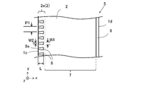
- FIG. 3 is an exploded perspective view schematically showing a wound film capacitor.
- 1 is a schematic cross-sectional view of a laminated film capacitor. It is a top view of the surface which shows a part of dielectric film and metal film in one of the embodiments. It is the iv-iv sectional view taken on the line of FIG.
- FIG. 5 is a cross-sectional view taken along the line vv of FIG. 3; It is the vi-vi line sectional view of FIG.
- It is a top view of the surface which shows a part of dielectric film and metal film in one of the embodiments.
- It is a top view of the surface which shows a part of dielectric film and metal film in one of the embodiments.
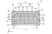
- the film capacitor comprises a film capacitor main body 3 (hereinafter sometimes referred to simply as the main body 3) and a pair of external electrodes 4a and 4b.
- a first dielectric film 1a, a second dielectric film 1b, a first metal film 2a, and a second metal film 2b are stacked or wound.
- the pair of external electrodes 4a and 4b are provided on opposite ends (main body ends) 3a and 3b of the main body 3 by metallikon.
- the main portion 3 of the wound film capacitor A shown in FIG. 1 comprises a first metallized film 5a having the first metal film 2a on the first surface 1ac of the first dielectric film 1a, and a second dielectric film
- the second metallized film 5b provided with the second metal film 2b is stacked and wound on the second surface 1bc of 1b.
- the first metal film 2 a is electrically connected to the external electrode 4 a at one main body end 3 a of the main body 3.
- the second metal film 2 b is electrically connected to the external electrode 4 b at the other main body end 3 b of the main body 3.
- the first of the first dielectric film 1a, the first metal film 2a, and the first metallized film 5a may be omitted, and may simply be referred to as the dielectric film 1a, the metal film 2a, and the metallized film 5a.
- the second of the second dielectric film 1b, the second metal film 2b and the second metallized film 5b may be omitted, and may simply be referred to as the dielectric film 1b, the metal film 2b and the metallized film 5b.
- the drawn dielectric films 1a and 1b and the metal films 2a and 2b are drawn to be thick enough to be in front of the paper.
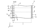
- the width direction of the dielectric films 1a and 1b and the metal films 2a and 2b is illustrated as a first direction x, the length direction as a second direction y, and the thickness direction as a z direction.
- the first direction x may be simply referred to as the x direction
- the second direction y may be simply referred to as the y direction.
- the dielectric films 1a and 1b and the metal films 2a and 2b are stacked in the z direction.
- the external electrodes 4a and 4b are disposed at the body end portions 3a and 3b located in the x direction of the body portion 3, respectively.
- the x direction coincides with the winding axial direction.
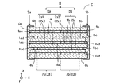
- the main part 3 of the laminated film capacitor B shown in FIG. 2 is a metallized film 5a having the metal film 2a on the first surface 1ac of the dielectric film 1a and a metal film on the second surface 1bc of the dielectric film 1b.
- Metallized films 5b provided with 2b are alternately laminated.
- the metal film 2 a is electrically connected to the external electrode 4 a at one main body end 3 a of the main body 3.
- the metal film 2 b is electrically connected to the external electrode 4 b at the other main body end 3 b of the main body 3.
- the dielectric film 1a of the film capacitors A and B has a first surface 1ac and a third surface 1ad opposed in the z direction, and a first side surface 1ae and a second side surface 1af opposed in the x direction.
- the dielectric film 1b has a second surface 1bc and a fourth surface 1bd opposite in the z direction, and a first side surface 1be and a second side surface 1bf opposite in the x direction.
- the metallized film 5a is obtained by forming the metal film 2a on the first surface 1ac of the dielectric film 1a, and an insulation margin continuously extending in the y direction in the vicinity of the second side surface 1af on the first surface 1ac. It has the part 6a.
- the insulation margin portion 6a is a portion where the dielectric film 1a is exposed.
- the metallized film 5b is obtained by forming the metal film 2b on the second surface 1bc of the dielectric film 1b, and an insulation margin continuously extending in the y direction in the vicinity of the second side surface 1bf on the second surface 1bc. It has the part 6b.
- the insulation margin portion 6 b is a portion where the dielectric film 1 b is exposed.
- the metallized films 5 a and 5 b are laminated or wound in a state of being slightly deviated in the width direction (x direction).
- the reference numerals a and b may be omitted.
- the z-direction which is the thickness direction of the film is enlarged and shown to facilitate the description.
- the film thickness of the metal film 2 may be, for example, 20 nm or less, in particular, 5 to 15 nm. By setting the metal film 2 to such a film thickness, the area resistance becomes 18 to 50 ⁇ / ⁇ , and the self-healing property can be exhibited. Area resistance may be called sheet resistance.
- a metal or alloy such as aluminum (Al) or zinc (Zn) may be used.
- the film thickness of the metal film 2 may be confirmed by, for example, a cross section of the metallized film 5 subjected to the ion milling process with a scanning electron microscope (SEM) or the like.
- SEM scanning electron microscope
- FIG. 3 is a plan view of the metallized film 5
- FIG. 4 is a cross-sectional view taken along line iv-iv of FIG. 3
- FIG. 5 is a cross-sectional view taken along line v-v of FIG. FIG.
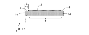
- the metal film 2 has a so-called heavy edge structure at least in the vicinity (2e) of the connection portion with the external electrode 4.
- the vicinity of the connection portion with the external electrode 4 is, in other words, the vicinity of the first side face 1 e of the dielectric film 1.
- the vicinity 2e of the connection portion between the metal film 2 and the external electrode 4 may be referred to as a heavy edge portion 2e or a first portion 2e.
- the heavy edge structure is, for example, a structure in which the thickness of the metal film 2 in the vicinity 2e of the connection portion with the external electrode 4 is large and the electric resistance is low, with respect to the effective region 7 where the metal films 2a and 2b overlap.
- the film thickness of the metal film 2 in the vicinity 2e of the connection portion with the external electrode 4 may be, for example, twice or more, specifically 20 nm or more, of the film thickness capable of exhibiting the self-healing property.
- the film thickness of the metal film 2 in the heavy edge portion 2e may be in the range of 80 nm or less.
- the equivalent series resistance (ESR) of the film capacitors A and B can be reduced by being electrically connected to the external electrode 4 by the heavy edge portion 2e having a low resistance.
- the heavy edge 2e of the metallized film 5a overlaps the insulation margin 6b of the metallized film 5b, and the heavy edge 2e of the metallized film 5b is the insulation margin of the metallized film 5a It may overlap with 6a.
- the width of the heavy edge portion 2e in the first direction x may be, for example, 4 mm or less, particularly 0.5 mm or more and 3 mm or less, depending on the size of the film capacitors A and B.
- the film thickness of the metal film 2 is thick, the influence of the difference between the thermal contraction rate of the metal film 2 and the thermal contraction rate of the dielectric film 1 is large. Therefore, at the end in the x direction of the metallized film 5, that is, at the main body end 3, warpage may occur in the metallized film 5 due to the thermal contraction difference between the metal film 2 and the dielectric film 1.
- the metallized film 5 has a warp at the end 3 of the main body, metallikon hardly enters the gap between the overlapping metallized films 5. As a result, the contact area between the metal film 2 and the external electrode 4 may be reduced, and the electrical connection between the metal film 2 and the external electrode 4 may not be sufficiently obtained.
- the metal film 2 has the first groove 8 extending in the first direction x in the heavy edge portion 2e.
- the first groove 8 has an opening 8 e opening at the body end 3 and has a predetermined length L in the first direction x from the opening 8 e.
- the length L of the first direction x of the first groove 8 may be the same as or shorter than the width of the heavy edge portion 2e in the first direction x as shown in FIG.
- the metal film 2 may have a plurality of first grooves 8 at predetermined intervals in the second direction y.
- the heavy edge portion 2 e having the first groove 8 By the heavy edge portion 2 e having the first groove 8, the influence of the thermal contraction difference between the metal film 2 and the dielectric film 1 at the heavy edge portion 2 e is alleviated by the first groove 8, and the metallized film 5 is obtained. Warpage of the end can be made less likely to occur. As a result, the reliability of the electrical connection between the metal film 2 and the external electrode 4 is improved, the dielectric loss of the film capacitor is reduced, and the increase of the dielectric loss due to charge and discharge cycles can be suppressed.
- the length L of the first direction x of the first groove 8 may be equal to or less than the width of the heavy edge portion 2e, that is, the first portion 2e in the first direction x.
- L may be, for example, 1.0 mm or more and 2.0 mm or less.
- L is larger than 1.0 mm, the influence of the thermal contraction difference with the dielectric film 1 can be alleviated.
- L is smaller than 2.0 mm, it is difficult for the first groove 8 to reach the effective area 7, and the capacitance can be secured. That is, the metal film 2 located in the effective region 7 may not have the first groove 8.
- the first groove 8a of the metallized film 5a may overlap with the margin portion 6b of the metallized film 5b and may not overlap with the metal film 2b.
- the first groove 8b of the metallized film 5b may overlap with the margin portion 6a of the metallized film 5a and may not overlap with the metal film 2a. That is, the first groove 8a of the metallized film 5a may not have a portion overlapping with the metal film 2b, and the first groove 8 of the metallized film 5b may not have a portion overlapping with the metal film 2a.
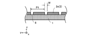
- the distance P1 between the first groove 8 and the first groove 8 adjacent in the second direction y may be, for example, 4 mm or less. If P1 is larger than 4 mm, there is a concern that the influence of the thermal contraction difference between the metal film 2 and the dielectric film 1 can not be alleviated. When the film thickness of the heavy edge portion 2e is relatively large, P1 may be decreased, and when the film thickness of the heavy edge portion 2e is relatively small, P1 may be increased. P1 may be, for example, 1 mm or more, but may be smaller than that.
- the width of the first groove 8 in the second direction y is W, as shown in FIG.
- W1 and W2 may be the same as shown in FIG.
- W1 may be larger than W2, that is, the width W2 of the opening 8e may be narrow, and the width W may be maximum at a portion of the first groove 8 other than the opening 8e.
- the shape of the first groove 8 may be rectangular as shown in FIG. 3, or as shown in FIG. 7, the opening 8e is a short bottom, and the side facing the opening 8e is a long bottom It may be trapezoidal.
- the shape of the first groove 8 may be a cross shape in which a groove extending in the first direction x and a groove extending in the second direction y intersect as shown in FIG.
- the length in the second direction y of the groove extending in the second direction y is taken as the maximum width W1.
- the metal film 2 which is the wall surface of the first groove 8 may be in contact with the main body end 3 across the first groove 8.
- the metal film 2 which is the wall surface of the first groove 8 at the body end 3 may not be joined.
- the shape of the first groove 8 may be a triangular shape having an apex at the body end 3.
- the ratio of the distance P1 between the adjacent first grooves 8 to the width W2 of the opening 8e is W2 / P1.
- W2 / P1 may be, for example, 0.35 or less.
- W1 may be, for example, 0.1 mm or more and 1.0 mm or less, particularly 0.3 mm or more and 0.5 mm or less.
- W2 may be, for example, 1.0 mm or less, in particular 0.5 mm or less.
- the bottom surface of the first groove 8 may be the dielectric film 1.
- the bottom surface of the first groove 8 may be the metal film 2.
- the thickness of the metal film 2 at the bottom of the first groove 8 is smaller than the thickness of the heavy edge 2 e.
- the metal film 2 may have one or more second grooves 9 in the effective region 7 in addition to the first grooves 8 as shown in FIG.
- the second groove 9 may be in contact with the end face 1 c of the dielectric film 1 and / or the insulation margin 6.
- the second groove 9 may extend in the first direction x and connect the end face 1 c of the dielectric film 1 and the insulation margin portion 6.
- the plurality of second grooves 9 may extend in different directions and intersect each other to divide the metal film 2 into a plurality of small regions.
- the metal film 2 may have a fuse portion 10 connecting the small regions divided by the second groove 9. When there are a plurality of second grooves 9 in the first region 2 e, one or more first grooves 8 may be disposed between the adjacent second grooves 9 and the second grooves 9.
- the distance P 1 between the first groove 8 and the first groove 8 is smaller than the distance P 2 between the second groove 9 and the second groove 9.
- the effective area 7 is divided into two in the first direction x
- the area adjacent to the insulation margin 6 of the metal film 2 has the second groove 9 and the heavy edge 2 e of the metal film 2.
- the region of H may not have the second groove 9.
- the width of the second groove 9 may be, for example, 0.01 to 0.20 mm.
- the second metallized film 5 b having the second metal film 2 b is alternately laminated on the second surface 1 bc of the film 1 b.
- the width direction of the first dielectric film 1a, the second dielectric film 1b, the first metal film 2a, and the second metal film 2b is the first direction x
- the length direction is the second direction y
- the thickness The direction is shown as the z direction.
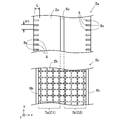
- the film capacitor C has two capacitive parts connected in series.
- the metal film 2a has a metal film 2a1 located on the left side of FIG. 11 and a metal film 2a2 located on the right side of FIG. That is, the metal film 2a has two metal films 2a1 and 2a2 arranged in the x direction.
- the metal film 2a1 is electrically connected to the external electrode 4a at the main body end 3a located on the left side of the main body portion 3, and the metal film 2a2 is connected to the external electrode 4b at the main body end 3b located on the right side of the main body 3 It is electrically connected.
- the metallized film 5a of the film capacitor C has a first insulation margin portion 6a continuously extending in the second direction y at a central portion in the first direction x.
- the metal film 2 is not formed, and the first surface 1ac is exposed.
- the metal film 2a1 and the metal film 2a2 are electrically insulated by the first insulation margin portion 6a.
- the metallized film 5b of the film capacitor C has a second insulation margin portion 6b continuously extending in the second direction y at both ends in the first direction x.
- the metal film 2 is not formed in the second insulation margin portion 6b, and the second surface 1bc is exposed.
- the metal film 2b is not electrically connected to any of the external electrodes 4a and 4b.
- the dielectric films 1a and 1b and the metal films 2a and 2b are stacked in the z direction and stacked as shown in FIG.
- the first capacity portion C1 and the second capacity portion C2 are connected in series.
- the first capacitance portion C1 is formed in the effective region 7a in which the metal film 2a1 and the metal film 2b sandwich the dielectric film 1a or 1b, and in the second capacitance portion C2, the metal film 2a2 and the metal film 2b are dielectrics It is formed in the effective area 7b sandwiching the body film 1a or 1b.
- any one of the overlapping metal films 2a (2a1, 2a2) and 2b may have a thickness that can exhibit self-healing properties.
- the entire metal film 2a of the film capacitor C may have the same thickness as that of the first portion 2e, and the total thickness of the metal film 2b may be 20 nm or less.
- the film capacitor C can exhibit self-healing property by the metal film 2b.
- the metal film 2a may have only the first groove 8 and the metal film 2b may have the second groove 9.
- Such a series type structure is not only applied to the laminated film capacitor C shown in FIGS. 10 and 11, but may be applied to a wound film capacitor.
- the first capacitance C1 and the second capacitance C2 are connected in series inside the film capacitor, and the voltage applied to the first capacitance C1 and the second capacitance The voltage applied to the part C2 is distributed according to the capacitance of each capacitive part. As a result, the withstand voltage of the entire film capacitor C can be improved.
- the film capacitors A and B may be referred to as a normal film capacitor, and the film capacitor C may be referred to as a series-connected film capacitor.
- the material of the insulating resin used for the dielectric film 1 is, for example, polypropylene (PP), polyethylene terephthalate (PET), polyphenylene sulfide (PPS), polyethylene naphthalate (PEN), polyarylate (PAR), polyphenylene ether (PPE) And polyetherimide (PEI) and cycloolefin polymer (COP).
- PP polypropylene
- PET polyethylene terephthalate
- PPS polyphenylene sulfide
- PEN polyethylene naphthalate
- PAR polyarylate
- PPE polyphenylene ether
- PEI polyetherimide
- COP cycloolefin polymer
- Polyarylates (PAR) in particular have high breakdown voltages.
- Such film capacitors A, B and C may be produced, for example, as follows.
- dielectric film 1 is prepared.
- the dielectric film 1 is formed, for example, by forming a resin solution in which an insulating resin is dissolved in a solvent on a surface of a substrate film made of polyethylene terephthalate (PET), for example, and drying to evaporate the solvent. can get.
- PET polyethylene terephthalate
- the forming method may be appropriately selected from known film forming methods such as a doctor blade method, a die coater method, and a knife coater method.
- a solvent used for molding for example, methanol, isopropanol, n-butanol, ethylene glycol, ethylene glycol monopropyl ether, methyl ethyl ketone, methyl isobutyl ketone, xylene, propylene glycol monomethyl ether, propylene glycol monomethyl ether acetate, dimethyl acetamide, cyclohexane
- an organic solvent containing a mixture of two or more selected from these Alternatively, a film of resin produced by a melt extrusion method may be stretched.
- the thickness of the dielectric film 1 may be, for example, 5 ⁇ m or less. In particular, it is preferable to use a dielectric film 1 having a thickness of 0.5 to 4 ⁇ m.
- the dielectric film 1 may be made of only the above-described insulating resin.
- the dielectric film 1 may contain materials other than the above-mentioned insulating resin.
- components other than resin contained in the dielectric film 1 the above-mentioned organic solvent and an inorganic filler are mentioned, for example.
- the inorganic filler for example, inorganic oxides such as alumina, titanium oxide and silicon dioxide, inorganic nitrides such as silicon nitride, and glass may be used.
- the inorganic filler may be subjected to surface treatment such as silane coupling treatment or titanate coupling treatment.
- the dielectric film 1 When such an inorganic filler is used for the dielectric film 1, a composite film containing less than 50% by mass of the inorganic filler and 50% by mass or more of the resin is used to maintain the flexibility of the resin while maintaining the flexibility. An effect such as improvement of the relative dielectric constant can be obtained.
- the size of the inorganic filler for example, the average particle size may be 4 to 1000 nm.
- a mask is applied to a predetermined portion of one surface of the produced dielectric film 1.
- a metal component such as aluminum (Al) is vapor-deposited on the non-masked portion of one surface of the dielectric film 1 to form the metal film 2, thereby obtaining the metallized film 5 having the insulation margin portion 6.
- the predetermined portion to be masked is one of the ends in the width direction (first direction x).
- the predetermined portion is the central portion in the width direction (first direction x) of the first dielectric film 1a, and both in the width direction (first direction x) of the second dielectric film 1b.
- the heavy edge structure is formed by masking, for example, zinc (Zn) further on the non-masked portion of the vapor-deposited metal component described above except for the portion forming the heavy edge of the metallized film 5 described above.
- the film thickness of the vapor deposition film to be vapor deposited to form the heavy edge portion 2e may be 1 to 3 times the film thickness of the above-mentioned vapor deposited metal component. As a result, the film thickness of the heavy edge portion 2e is 2 to 4 times the film thickness of the other portion, and becomes the first portion 2e.
- the first groove 8 is formed in the first portion 2 e of the metal film 2.
- Laser patterning may be used to form the first groove 8.
- the laser patterning method is a method of evaporating a part of the metal film 4 by a laser, and uses a laser marker machine or a laser trimmer machine.
- the laser any one of a green laser, a YAG laser and a CO 2 laser may be used.
- the metallized film 5 (5a, 5b) having the metal film 2 (2a, 2b) on one side is a little in the width direction, ie, in the first direction x, as shown in FIG.
- the main body 3 of the film capacitor A or B is obtained by stacking one or more sets in a shifted state and laminating or winding.
- the main body 3 of the film capacitor C is obtained by stacking the metallized films 5a and 5b as a set, and stacking one or more sets as shown in FIG. 11, or winding.
- Film capacitors A, B, or C can be obtained by forming metallikon electrodes as external electrodes 4 on both end surfaces of the obtained main body portion 3 in the x direction.
- a method such as thermal spraying of metal, sputtering, plating or the like may be used.
- the outer surface of the main body 3 on which the external electrode 4 is formed may be covered with an exterior member (not shown).
- Examples of the material of the metal film 2 include metals or alloys such as aluminum (Al) and zinc (Zn).
- At least one metal material selected from zinc, tin, aluminum, copper and solder may be used as the material of the metallikon electrode.
- FIG. 12 is a perspective view schematically showing one of the embodiments of the coupled capacitor.
- the connection type capacitor D a plurality of wound film capacitors A are connected in parallel by a pair of bus bars 21 and 23.
- the bus bars 21 and 23 have terminal portions 21 a and 23 a for external connection and lead terminal portions 21 b and 23 b.
- the leadout terminal portions 21b and 23b are respectively connected to the external electrodes 4a and 4b of the film capacitor A.
- connection type capacitor D may include a laminated type film capacitor B or a series connection type film capacitor C in place of the wound type film capacitor A.
- the connected capacitor D may have at least one film capacitor A, or may have two or more film capacitors A.
- the connection type capacitor D in a state where a plurality of film capacitors A are arranged, for example, four as shown in FIG. 12, the external electrodes 4a and 4b respectively formed on both ends of the main body 3 It is obtained by attaching 21 and 23.
- the connected capacitor D may have a flat film capacitor, or may have a stacked film capacitor.
- the film capacitor A may be arranged such that the direction in which the external electrode 4 is located, that is, the x direction is along the vertical direction.
- the film capacitors A, B and C and the connected capacitor D may be housed in a case and then filled with resin in the space in the case to form a resin mold type (case mold type) capacitor.
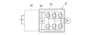
- FIG. 13 is a schematic configuration diagram for describing an embodiment of an inverter.
- FIG. 13 shows an inverter E that generates alternating current from direct current as an example of the embodiment.
- the inverter E includes a bridge circuit 31 and a capacitance unit 33, as shown in FIG.
- the bridge circuit 31 includes, for example, a switching element such as an IGBT (Insulated gate Bipolar Transistor) and a diode.
- the capacitive unit 33 is disposed between the input terminals of the bridge circuit 31 to stabilize the voltage.
- the above-described film capacitors A, B, and C or a connection type capacitor D are used as the capacitor portion 33.
- the inverter E is connected to a booster circuit 35 that boosts the voltage of the DC power supply.
- the bridge circuit 31 is connected to a motor generator (motor M) as a driving source.
- FIG. 14 is a schematic block diagram of an electric vehicle.
- FIG. 14 shows a hybrid vehicle (HEV) as an example of the embodiment.
- HEV hybrid vehicle
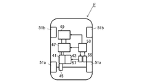
- the electric powered vehicle F includes a drive motor 41, an engine 43, a transmission 45, an inverter 47, a power supply (battery) 49, a front wheel 51a and a rear wheel 51b.
- the electric powered vehicle F is provided with an output of a motor 41, an engine 43, or both as a drive source.
- the output of the drive source is transmitted to the pair of left and right front wheels 51 a via the transmission 45.
- the power supply 49 is connected to the inverter 47, and the inverter 47 is connected to the motor 41.
- the electric powered vehicle F shown in FIG. 14 includes a vehicle ECU 53 and an engine ECU 57.
- the vehicle ECU 53 performs overall control of the entire electric powered vehicle E.
- the engine ECU 57 controls the rotational speed of the engine 43 to drive the electric vehicle E.
- the electric powered vehicle E further includes an ignition key 55 operated by a driver or the like, an accelerator pedal (not shown), and a driving device such as a brake.
- the vehicle ECU 53 receives a drive signal according to the operation of the drive device by the driver or the like.
- the vehicle ECU 53 outputs an instruction signal to the engine ECU 57, the power supply 49, and the inverter 47 as a load based on the drive signal.
- Engine ECU 57 controls the number of rotations of engine 43 in response to the instruction signal, and drives electrically powered vehicle E.
- an inverter E that is, the inverter E including the above film capacitors A, B, C or a coupled capacitor D in the capacity portion 33 is used.
- the film capacitors A, B, C or the coupled capacitor D have small dielectric loss and little increase in dielectric loss due to charge and discharge cycles, so the electrostatic capacitance is extended for a long time The switching noise generated by the inverter 47 can be reduced for a long time.
- the inverter E of this embodiment can be applied not only to the above-mentioned hybrid vehicle (HEV) but also to various power conversion application products such as an electric vehicle (EV), a fuel cell vehicle, or an electric bicycle, a generator, a solar cell .
- EV electric vehicle
- a fuel cell vehicle or an electric bicycle
- a generator a solar cell .
- a dielectric film having an average thickness of 2.5 ⁇ m was produced using polyarylate (U-100, manufactured by Unitika).
- the dielectric film was prepared by dissolving polyarylate in toluene, applying it on a substrate made of polyethylene terephthalate (PET) using a coater, and forming it into a sheet. After molding, heat treatment was performed at 130 ° C. to remove toluene, and a dielectric film was obtained. The obtained dielectric film was peeled from the substrate and slit into a width of 130 mm.
- a series connected film capacitor was produced as follows.
- An Al (aluminum) metal film was formed on one main surface of the dielectric film to obtain a metallized film having two types of metal films different in film thickness.
- a thick metal film is referred to as a first metal film
- a thin metal film is referred to as a second metal film.
- the film thickness of the metal film was determined by scanning electron microscope (SEM) observation of a cross section subjected to ion milling.
- the film thickness t1 of the first metal film and the film thickness t2 of the second metal film are shown in Table 1.
- the sheet resistance was evaluated in a 4-terminal resistance measurement mode using a multimeter. For example, the sheet resistance of the metal film with a film thickness of 50 nm was 7 ⁇ / ⁇ , and the sheet resistance of the metal film with a film thickness of 30 nm was 25 ⁇ / ⁇ .
- a 2 mm wide first insulation margin is formed at the center of the first metal film in the first direction x using a green laser marker, and the second insulation margin is formed at both ends of the second metal film in the first direction x Formed.
- the first groove was formed at both ends in the first direction x of the thick first metal film, that is, at the first portion.
- the shape of the first groove is shown in Table 1.
- a second groove was formed in a mesh shape on the entire surface using a green laser marker.
- a second groove formed a pattern composed of a small area of 2 mm ⁇ 2 mm and a fuse part having a width of 0.2 mm connecting the small areas.
- the laser irradiation conditions were an output of 4 W, a frequency of 140 kHz, and a scanning speed of 4 m / sec.
- a 130 mm wide metallized film is further slitted, and a first metallized film having a first metal film is a 28 mm wide metallized film having a first insulation margin portion with a width of 2 mm at a central portion in a first direction x.
- the second metallized film having the second metal film was a metallized film with a total width of 27 mm, having a second insulation margin portion with a width of 1.5 mm at both ends in the first direction x.
- the first metallized film and the second metallized film were superposed, and wound 100 times on a drum with a diameter of 200 mm, to obtain a wound body in which a plurality of film capacitors are annularly connected.
- the first metallized film and the second metallized film were laminated so as to sandwich a single dielectric film between the first metal film and the second metal film.
- the conventional film capacitor was produced as follows. An oil mask was used on one surface of the dielectric film slitted to a width of 130 mm, and an Al (aluminum) metal film having a width of 52 mm was formed at the center in the width direction which is the first direction x. The average thickness of the Al metal film was 15 nm. Next, a Zn (zinc) metal film having a width of 2 to 8 mm was formed at the center in the width direction of the formed Al metal film as a heavy edge portion using a metal mask. The average thickness of the Zn metal film was 5 to 65 nm.
- the center and both ends in the width direction of the obtained metallized film were slit to obtain a first metallized film and a second metallized film having a width of 28 mm.
- the width of the insulation margin of each metallized film obtained was 1 mm, and the width of the heavy edge was 1 to 4 mm.
- a first groove was formed in the heavy edge portion or first portion of the first metal film and the second metal film using a green laser marker.
- the shape of the first groove is shown in Table 2.
- a second groove is formed in a mesh shape using a green laser marker in a region closer to the insulation margin portion than the center of the first metal film and the second metal film in the first direction, and a small 2 mm ⁇ 2 mm
- a pattern was formed of a region and a 0.2 mm wide fuse portion connecting between the small regions.
- the laser irradiation conditions were an output of 4 W, a frequency of 140 kHz, and a scanning speed of 4 m / sec.
- the heavy edge portions of the first metallized film and the second metallized film are located on the opposite side of the first direction x, and the respective heavy edge portions protrude 0.5 mm in the first direction x , Overlaid.
- One set of the metallized films thus stacked was wound 100 times on a drum having a diameter of 200 mm to obtain a wound body in which a plurality of film capacitors were connected in an annular shape.
- the first metallized film and the second metallized film were laminated so as to sandwich a single dielectric film between the first metal film and the second metal film.
- the obtained wound body was cut so that the width in the second direction y was 15 mm, to obtain a laminate as a main body.
- An alloy of zinc and tin was sprayed on the end face of the main body in the first direction x to form a metallikon electrode as an external electrode to obtain a film capacitor.
- the dielectric loss (DF) of the produced film capacitor was measured using a digital multimeter under conditions of 1 V AC and 1 kHz. The value of this dielectric loss is taken as dielectric loss DF1 before the charge and discharge test.
- the charge / discharge test of the film capacitor was performed as follows. After charging the film capacitor with a DC voltage (DC) of 600 V, a forced short circuit was performed to discharge. A charge / discharge test of 100 cycles was performed on a charge / discharge cycle in which one charge-discharge cycle was one cycle. After the charge and discharge test, the dielectric loss DF was measured again, and the obtained value was taken as the dielectric loss DF2 after the charge and discharge test.
- the values of DF1, DF2 and DF2 / DF1 are listed in Table 1.
- DF2 / DF1 is the ratio of DF2 to DF1.
- Sample No. 1 having a first groove at the end in the first direction of the thick first metal film that is, the first portion. 2, 3, 5 to 17, 19, 20, and a sample No. 1 having a heavy edge portion, ie, a first groove at a first portion. 22, 23, 25, 26, 28 to 36, 38, 40 and 41 have sample Nos. 1 and 2 that do not have a first groove.
- the increase in dielectric loss after the charge and discharge test was small.
- sample No. 1 in which the maximum width W1 of the first groove is larger than the width W2 of the opening portion No increase in dielectric loss was observed after the charge / discharge test in any of 3, 14, 16 to 20, 23, 26, 33 to 35 and 41.
- A, B, C film capacitor D: connected capacitor E: inverter F: electric vehicle 1, 1a, 1b: dielectric film 2, 2a, 2b: metal film 2e: first portion (heavy edge portion) 3: Body part 4, 4a, 4b: External electrode 5, 5a, 5b: Metallized film 7: Effective area 8: First groove 9: Second groove 10: Fuse part 21, 23: Bus bar 31: Bridge circuit 33: Capacity section 35: Boost circuit 41: Motor 43: Engine 45: Transmission 47: Inverter 49: Power supply 51a: Front wheel 51b: Rear wheel 53: Vehicle ECU 55: Ignition key 57: Engine ECU
Landscapes
- Engineering & Computer Science (AREA)
- Power Engineering (AREA)
- Microelectronics & Electronic Packaging (AREA)
- Manufacturing & Machinery (AREA)
- Fixed Capacitors And Capacitor Manufacturing Machines (AREA)
- Inverter Devices (AREA)
Abstract
Provided is a film capacitor equipped with: a body 3 provided with at least a first metalized film having a first metal film 2a on a first surface of a first dielectric film 1a, and a second metalized film 5b having a second metal film 2b on a second surface of a second dielectric film 1b; and a pair of external electrodes 4a, 4b. The first dielectric film 1a and the second dielectric film 2b are disposed between the first metal film 2a and the second metal film 2b. The external electrodes 4a, 4b are respectively disposed on a pair of body end parts 3a, 3b in a first direction of the body 3, and are electrically connected to the first metal film 2a and the second metal film 2b. At least one of the first and second metal films 2a, 2b electrically connected to the external electrodes 4a, 4b has a first region 2e having a film thickness of 20 nm or greater, the first region 2e being near the body end parts 3a, 3b electrically connected to the external electrodes 4a, 4b, and a first groove 8 that contacts the body end part 3a or 3b and extends in the first direction is provided to the first region 2e.
Description
本開示は、フィルムコンデンサ、連結型コンデンサと、これを用いたインバータおよび電動車輌に関するものである。
The present disclosure relates to a film capacitor, a coupled capacitor, an inverter using the same, and an electric vehicle.
フィルムコンデンサは、例えば、ポリプロピレン樹脂をフィルム化した誘電体フィルムと、当該誘電体フィルムの表面に蒸着によって形成された金属膜と、を有している。金属膜は電極として用いられる。このような構成により、フィルムコンデンサでは、誘電体フィルムの絶縁欠陥部で短絡が生じた場合にも、短絡のエネルギーで欠陥部周辺の金属膜が蒸発、飛散し、誘電体フィルムの絶縁欠陥部が絶縁化される。フィルムコンデンサは、このような自己回復性を有し、絶縁破壊し難い。
The film capacitor has, for example, a dielectric film obtained by filming a polypropylene resin, and a metal film formed on the surface of the dielectric film by vapor deposition. A metal film is used as an electrode. With such a configuration, in the film capacitor, even when a short circuit occurs in the insulation defect portion of the dielectric film, the metal film around the defect portion is evaporated and scattered by the energy of the short circuit, and the insulation defect portion of the dielectric film is It is insulated. The film capacitor has such self-healing property and is hard to break down.
このように、フィルムコンデンサは電気回路が短絡した際の発火や感電を発生させ難い。そのため、近年、フィルムコンデンサの用途は、LED(Light Emitting Diode)照明等の電源回路、ハイブリッド自動車のモータ駆動、太陽光発電のインバータシステム等に拡大しつつある。
As described above, the film capacitor is unlikely to generate a fire or an electric shock when the electric circuit is short-circuited. Therefore, in recent years, applications of film capacitors are being expanded to power supply circuits such as light emitting diode (LED) lighting, motor drive of hybrid vehicles, inverter systems for solar power generation, and the like.
フィルムコンデンサにおいて、上述のような自己回復性を有する容量発現部の金属膜の厚さに対し、外部電極と接続する部位の金属膜の厚さを厚くし、金属膜と外部電極との接続強度をあげる技術が、例えば特許文献1に開示されている。
In the film capacitor, the thickness of the metal film at the portion connected to the external electrode is made thicker than the thickness of the metal film of the capacity developing portion having self-healing property as described above, and the connection strength between the metal film and the external electrode For example, Patent Document 1 discloses a technique for raising
本開示のフィルムコンデンサは、第1誘電体フィルム、および該第1誘電体フィルムの第1面上に配置された第1金属膜を有する第1金属化フィルムと、第2誘電体フィルム、および第2誘電体フィルムの第2面上に配置された第2金属膜を有する第2金属化フィルムと、を少なくとも備える本体部と、一対の外部電極と、を具備する。前記第1金属膜と前記第2金属膜との間には、前記第1誘電体フィルムまたは前記第2誘電体フィルムが配置されている。前記外部電極は、前記本体部の第1方向の一対の本体端部にそれぞれ配置され、前記第1金属膜および前記第2金属膜のいずれか一方に電気的に接続されている。前記外部電極と電気的に接続している前記第1金属膜および/または前記第2金属膜は、前記外部電極と電気的に接続する前記本体端部の近傍に、膜厚が20nm以上の第1部位を有するとともに、該第1部位に、前記本体端部に接し、前記第1方向に延びる複数の第1の溝を有する。なお、「Aおよび/またはB」と記載した時、これは「Aのみ」、「Bのみ」、または「AおよびB」のうちいずれかを指す。
The film capacitor of the present disclosure comprises: a first dielectric film; a first metallized film having a first metal film disposed on a first surface of the first dielectric film; a second dielectric film; A second metallized film having a second metal film disposed on a second surface of the second dielectric film, and a main body including at least a pair of external electrodes. The first dielectric film or the second dielectric film is disposed between the first metal film and the second metal film. The external electrodes are respectively disposed at a pair of main body end portions in the first direction of the main body portion, and are electrically connected to any one of the first metal film and the second metal film. The first metal film and / or the second metal film electrically connected to the external electrode may have a thickness of 20 nm or more in the vicinity of the end portion of the main body electrically connected to the external electrode. It has one portion, and the first portion has a plurality of first grooves in contact with the body end and extending in the first direction. In addition, when it describes as "A and / or B", this refers to either "A only", "B only", or "A and B."
本開示の連結型コンデンサは、複数のフィルムコンデンサと、該複数のフィルムコンデンサを接続するバスバーと、を備え、前記フィルムコンデンサが、上記のフィルムコンデンサを含む。
The coupled capacitor of the present disclosure includes a plurality of film capacitors and a bus bar connecting the plurality of film capacitors, and the film capacitor includes the above-described film capacitor.
本開示のインバータは、スイッチング素子を有するブリッジ回路と、該ブリッジ回路に接続された容量部とを備え、前記容量部が上記のフィルムコンデンサを含む。
The inverter of the present disclosure includes a bridge circuit having a switching element, and a capacitor connected to the bridge circuit, the capacitor including the above-described film capacitor.
本開示の電動車輌は、電源と、該電源に接続されたインバータと、該インバータに接続されたモータと、該モータにより駆動する車輪と、を備え、前記インバータが上記のインバータである。
The electric vehicle of the present disclosure includes a power supply, an inverter connected to the power supply, a motor connected to the inverter, and a wheel driven by the motor, and the inverter is the above-described inverter.
フィルムコンデンサは、図1~図3に示すように、フィルムコンデンサ本体部3(以下、単に本体部3という場合もある)と、一対の外部電極4a、4bとを具備している。本体部3は、第1誘電体フィルム1a、第2誘電体フィルム1bと、第1金属膜2a、第2金属膜2bとが積層または捲回されている。一対の外部電極4a、4bは、本体部3の対向する端部(本体端部)3a、3bにメタリコンにより設けられている。
As shown in FIGS. 1 to 3, the film capacitor comprises a film capacitor main body 3 (hereinafter sometimes referred to simply as the main body 3) and a pair of external electrodes 4a and 4b. In the main body portion 3, a first dielectric film 1a, a second dielectric film 1b, a first metal film 2a, and a second metal film 2b are stacked or wound. The pair of external electrodes 4a and 4b are provided on opposite ends (main body ends) 3a and 3b of the main body 3 by metallikon.
図1に示す捲回型のフィルムコンデンサAの本体部3は、第1誘電体フィルム1aの第1面1acに第1金属膜2aを備えた第1金属化フィルム5aと、第2誘電体フィルム1bの第2面1bcに第2金属膜2bを備えた第2金属化フィルム5bとが重ねられ、捲回されている。第1金属膜2aは本体部3の一方の本体端部3aで外部電極4aに電気的に接続されている。第2金属膜2bは、本体部3の他方の本体端部3bで外部電極4bに電気的に接続されている。以下、第1誘電体フィルム1a、第1金属膜2aおよび第1金属化フィルム5aの第1を省略し、単に誘電体フィルム1a、金属膜2aおよび金属化フィルム5aという場合がある。また、第2誘電体フィルム1b、第2金属膜2bおよび第2金属化フィルム5bの第2を省略し、単に誘電体フィルム1b、金属膜2bおよび金属化フィルム5bという場合がある。
The main portion 3 of the wound film capacitor A shown in FIG. 1 comprises a first metallized film 5a having the first metal film 2a on the first surface 1ac of the first dielectric film 1a, and a second dielectric film The second metallized film 5b provided with the second metal film 2b is stacked and wound on the second surface 1bc of 1b. The first metal film 2 a is electrically connected to the external electrode 4 a at one main body end 3 a of the main body 3. The second metal film 2 b is electrically connected to the external electrode 4 b at the other main body end 3 b of the main body 3. Hereinafter, the first of the first dielectric film 1a, the first metal film 2a, and the first metallized film 5a may be omitted, and may simply be referred to as the dielectric film 1a, the metal film 2a, and the metallized film 5a. In addition, the second of the second dielectric film 1b, the second metal film 2b and the second metallized film 5b may be omitted, and may simply be referred to as the dielectric film 1b, the metal film 2b and the metallized film 5b.
図1では、理解を容易にするために、引き出した誘電体フィルム1a、1bおよび金属膜2a、2bの厚みを紙面の手前にくる程厚くなるように描いている。
In FIG. 1, in order to facilitate understanding, the drawn dielectric films 1a and 1b and the metal films 2a and 2b are drawn to be thick enough to be in front of the paper.
図1では、誘電体フィルム1a、1bおよび金属膜2a、2bの幅方向を第1方向x、長さ方向を第2方向y、厚さ方向をz方向として示している。以下、第1方向xを単にx方向といい、第2方向yを単にy方向という場合がある。誘電体フィルム1a、1bおよび金属膜2a、2bはz方向に重ねあわされている。外部電極4a、4bは本体部3のx方向に位置する本体端部3a、3bにそれぞれ配置されている。フィルムコンデンサAでは、x方向は捲回の軸方向と一致する。
In FIG. 1, the width direction of the dielectric films 1a and 1b and the metal films 2a and 2b is illustrated as a first direction x, the length direction as a second direction y, and the thickness direction as a z direction. Hereinafter, the first direction x may be simply referred to as the x direction, and the second direction y may be simply referred to as the y direction. The dielectric films 1a and 1b and the metal films 2a and 2b are stacked in the z direction. The external electrodes 4a and 4b are disposed at the body end portions 3a and 3b located in the x direction of the body portion 3, respectively. In the film capacitor A, the x direction coincides with the winding axial direction.
図2に示す積層型のフィルムコンデンサBの本体部3は、誘電体フィルム1aの第1面1acに金属膜2aを備えた金属化フィルム5aと、誘電体フィルム1bの第2面1bcに金属膜2bを備えた金属化フィルム5bとが交互に積層されている。金属膜2aは本体部3の一方の本体端部3aで外部電極4aに電気的に接続されている。金属膜2bは、本体部3の他方の本体端部3bで外部電極4bに電気的に接続されている。
The main part 3 of the laminated film capacitor B shown in FIG. 2 is a metallized film 5a having the metal film 2a on the first surface 1ac of the dielectric film 1a and a metal film on the second surface 1bc of the dielectric film 1b. Metallized films 5b provided with 2b are alternately laminated. The metal film 2 a is electrically connected to the external electrode 4 a at one main body end 3 a of the main body 3. The metal film 2 b is electrically connected to the external electrode 4 b at the other main body end 3 b of the main body 3.
フィルムコンデンサAおよびBの誘電体フィルム1aは、z方向に対向する第1面1acと第3面1ad、およびx方向に対向する第1側面1aeと第2側面1afを有している。誘電体フィルム1bは、z方向に対向する第2面1bcと第4面1bd、およびx方向に対向する第1側面1beと第2側面1bfを有している。
The dielectric film 1a of the film capacitors A and B has a first surface 1ac and a third surface 1ad opposed in the z direction, and a first side surface 1ae and a second side surface 1af opposed in the x direction. The dielectric film 1b has a second surface 1bc and a fourth surface 1bd opposite in the z direction, and a first side surface 1be and a second side surface 1bf opposite in the x direction.
金属化フィルム5aとは、誘電体フィルム1aの第1面1ac上に金属膜2aを形成したものであり、第1面1ac上の第2側面1af近傍に、y方向に連続して延びる絶縁マージン部6aを有している。絶縁マージン部6aは、誘電体フィルム1aが露出した部分である。
The metallized film 5a is obtained by forming the metal film 2a on the first surface 1ac of the dielectric film 1a, and an insulation margin continuously extending in the y direction in the vicinity of the second side surface 1af on the first surface 1ac. It has the part 6a. The insulation margin portion 6a is a portion where the dielectric film 1a is exposed.
金属化フィルム5bとは、誘電体フィルム1bの第2面1bc上に金属膜2bを形成したものであり、第2面1bc上の第2側面1bf近傍に、y方向に連続して延びる絶縁マージン部6bを有している。絶縁マージン部6bは、誘電体フィルム1bが露出した部分である。
The metallized film 5b is obtained by forming the metal film 2b on the second surface 1bc of the dielectric film 1b, and an insulation margin continuously extending in the y direction in the vicinity of the second side surface 1bf on the second surface 1bc. It has the part 6b. The insulation margin portion 6 b is a portion where the dielectric film 1 b is exposed.
図1、2に示すように、金属化フィルム5a、5bは、少し幅方向(x方向)にずれた状態で積層または捲回されている。
As shown in FIGS. 1 and 2, the metallized films 5 a and 5 b are laminated or wound in a state of being slightly deviated in the width direction (x direction).
金属膜2aと金属膜2bとの間に電位差があると、金属膜2aと金属膜2bとが誘電体フィルム1aまたは誘電体フィルム1bを挟んで重なり合う有効領域7に、静電容量が発生する。
When there is a potential difference between the metal film 2a and the metal film 2b, electrostatic capacitance is generated in the effective region 7 in which the metal film 2a and the metal film 2b overlap with the dielectric film 1a or the dielectric film 1b interposed therebetween.
フィルムコンデンサAおよびBの金属化フィルム5a、5bに共通する本実施形態の特徴について説明するため、以下では、図3に示すように、a、bの符号を省略する場合がある。また、図4等の断面図においては、説明を容易にするためにフィルムの厚さ方向であるz方向を拡大して示している。
In order to describe the features of the present embodiment common to the metallized films 5a and 5b of the film capacitors A and B, in the following, as shown in FIG. 3, the reference numerals a and b may be omitted. Further, in the cross-sectional views of FIG. 4 and the like, the z-direction which is the thickness direction of the film is enlarged and shown to facilitate the description.
金属膜2の膜厚は、例えば20nm以下、特には5~15nmの範囲とするのがよい。金属膜2をこのような膜厚とすることで、面積抵抗が18~50Ω/□となり、自己回復性を発揮できる。面積抵抗をシート抵抗という場合もある。金属膜2の材料としては、たとえばアルミニウム(Al)、亜鉛(Zn)などの金属または合金などを用いてもよい。
The film thickness of the metal film 2 may be, for example, 20 nm or less, in particular, 5 to 15 nm. By setting the metal film 2 to such a film thickness, the area resistance becomes 18 to 50 Ω / □, and the self-healing property can be exhibited. Area resistance may be called sheet resistance. As a material of the metal film 2, for example, a metal or alloy such as aluminum (Al) or zinc (Zn) may be used.
金属膜2の膜厚は、たとえばイオンミリング加工をした金属化フィルム5の断面を走査型電子顕微鏡(SEM)などで確認すればよい。
The film thickness of the metal film 2 may be confirmed by, for example, a cross section of the metallized film 5 subjected to the ion milling process with a scanning electron microscope (SEM) or the like.
図3は金属化フィルム5の平面図であり、図4は図3のiv-iv線断面図、図5は図3のv-v線断面図、図6は図3のvi-vi線断面図である。金属膜2は、図3、4に示すように、少なくとも外部電極4との接続部の近傍(2e)に、いわゆるヘビーエッジ構造を有している。外部電極4との接続部の近傍とは、言い換えると誘電体フィルム1の第1側面1eの近傍である。以下、金属膜2の外部電極4との接続部の近傍2eを、ヘビーエッジ部2eまたは第1部位2eという場合もある。ヘビーエッジ構造とは、たとえば金属膜2a、2b同士が重なり合う有効領域7に対して、外部電極4との接続部の近傍2eにおける金属膜2の厚さが厚く、電気抵抗が低い構造である。外部電極4との接続部の近傍2eにおける金属膜2の膜厚は、たとえば自己回復性を発揮できる膜厚の2倍以上、具体的には20nm以上としてもよい。ヘビーエッジ部2eにおける金属膜2の膜厚は、80nm以下の範囲としてもよい。金属膜2がヘビーエッジ部2eを有することにより、金属膜2と外部電極4との電気的接続が向上する。また、抵抗の低いヘビーエッジ部2eにより外部電極4と電気的に接続されることで、フィルムコンデンサAおよびBの等価直列抵抗(ESR)を低減することができる。フィルムコンデンサAおよびBにおいて、金属化フィルム5aのヘビーエッジ部2eは、金属化フィルム5bの絶縁マージン部6bと重なりあい、金属化フィルム5bのヘビーエッジ部2eは、金属化フィルム5aの絶縁マージン部6aと重なり合っていてもよい。ヘビーエッジ部2eの第1方向xの幅は、フィルムコンデンサAおよびBのサイズに応じて、たとえば4mm以下、特には0.5mm以上、3mm以下としてもよい。
3 is a plan view of the metallized film 5, FIG. 4 is a cross-sectional view taken along line iv-iv of FIG. 3, FIG. 5 is a cross-sectional view taken along line v-v of FIG. FIG. As shown in FIGS. 3 and 4, the metal film 2 has a so-called heavy edge structure at least in the vicinity (2e) of the connection portion with the external electrode 4. The vicinity of the connection portion with the external electrode 4 is, in other words, the vicinity of the first side face 1 e of the dielectric film 1. Hereinafter, the vicinity 2e of the connection portion between the metal film 2 and the external electrode 4 may be referred to as a heavy edge portion 2e or a first portion 2e. The heavy edge structure is, for example, a structure in which the thickness of the metal film 2 in the vicinity 2e of the connection portion with the external electrode 4 is large and the electric resistance is low, with respect to the effective region 7 where the metal films 2a and 2b overlap. The film thickness of the metal film 2 in the vicinity 2e of the connection portion with the external electrode 4 may be, for example, twice or more, specifically 20 nm or more, of the film thickness capable of exhibiting the self-healing property. The film thickness of the metal film 2 in the heavy edge portion 2e may be in the range of 80 nm or less. By the metal film 2 having the heavy edge portion 2 e, the electrical connection between the metal film 2 and the external electrode 4 is improved. Further, the equivalent series resistance (ESR) of the film capacitors A and B can be reduced by being electrically connected to the external electrode 4 by the heavy edge portion 2e having a low resistance. In the film capacitors A and B, the heavy edge 2e of the metallized film 5a overlaps the insulation margin 6b of the metallized film 5b, and the heavy edge 2e of the metallized film 5b is the insulation margin of the metallized film 5a It may overlap with 6a. The width of the heavy edge portion 2e in the first direction x may be, for example, 4 mm or less, particularly 0.5 mm or more and 3 mm or less, depending on the size of the film capacitors A and B.
ヘビーエッジ部2eでは、金属膜2の膜厚が厚いため、金属膜2の熱収縮率と誘電体フィルム1の熱収縮率との差の影響が大きい。そのため、金属化フィルム5のx方向の端部、すなわち本体端部3では、金属膜2と誘電体フィルム1との熱収縮差に起因して金属化フィルム5に反りが発生する場合がある。本体端部3で金属化フィルム5が反りを有すると、重なり合う金属化フィルム5の間隙にメタリコンが入りにくくなる。その結果、金属膜2と外部電極4との接触面積が小さくなって、金属膜2と外部電極4との電気的接続が十分に得られない場合があった。
In the heavy edge portion 2 e, since the film thickness of the metal film 2 is thick, the influence of the difference between the thermal contraction rate of the metal film 2 and the thermal contraction rate of the dielectric film 1 is large. Therefore, at the end in the x direction of the metallized film 5, that is, at the main body end 3, warpage may occur in the metallized film 5 due to the thermal contraction difference between the metal film 2 and the dielectric film 1. When the metallized film 5 has a warp at the end 3 of the main body, metallikon hardly enters the gap between the overlapping metallized films 5. As a result, the contact area between the metal film 2 and the external electrode 4 may be reduced, and the electrical connection between the metal film 2 and the external electrode 4 may not be sufficiently obtained.
本開示の実施形態の一つでは、図3~6に示すように、金属膜2が、ヘビーエッジ部2eに、第1方向xに延びる第1の溝8を有している。第1の溝8は、本体端部3に開口する開口部8eを有し、開口部8eから第1方向xに、所定の長さLを有している。第1の溝8の第1方向xの長さLは、図3のようにヘビーエッジ部2eの第1方向xの幅と同じ、または短くてもよい。金属膜2は、第2方向yに所定の間隔で複数の第1の溝8を有していてもよい。
In one of the embodiments of the present disclosure, as shown in FIGS. 3 to 6, the metal film 2 has the first groove 8 extending in the first direction x in the heavy edge portion 2e. The first groove 8 has an opening 8 e opening at the body end 3 and has a predetermined length L in the first direction x from the opening 8 e. The length L of the first direction x of the first groove 8 may be the same as or shorter than the width of the heavy edge portion 2e in the first direction x as shown in FIG. The metal film 2 may have a plurality of first grooves 8 at predetermined intervals in the second direction y.
ヘビーエッジ部2eが第1の溝8を有することにより、ヘビーエッジ部2eにおける金属膜2と誘電体フィルム1との熱収縮差の影響が第1の溝8により緩和され、金属化フィルム5の端部の反りを発生し難くすることができる。その結果、金属膜2と外部電極4との電気的接続の信頼性が向上し、フィルムコンデンサの誘電損失が低減され、充放電サイクルによる誘電損失の増大を抑えることができる。
By the heavy edge portion 2 e having the first groove 8, the influence of the thermal contraction difference between the metal film 2 and the dielectric film 1 at the heavy edge portion 2 e is alleviated by the first groove 8, and the metallized film 5 is obtained. Warpage of the end can be made less likely to occur. As a result, the reliability of the electrical connection between the metal film 2 and the external electrode 4 is improved, the dielectric loss of the film capacitor is reduced, and the increase of the dielectric loss due to charge and discharge cycles can be suppressed.
第1の溝8の第1方向xの長さLは、ヘビーエッジ部2eすなわち第1部位2eの第1方向xの幅以下であってもよい。Lは、たとえば1.0mm以上、2.0mm以下としてもよい。Lが1.0mmより大きいことで、誘電体フィルム1との熱収縮差の影響を緩和することができる。Lが2.0mmより小さいことで、第1の溝8が有効領域7に達し難くなり、静電容量を確保することができる。すなわち、有効領域7に位置する金属膜2は、第1の溝8を有していなくてもよい。
The length L of the first direction x of the first groove 8 may be equal to or less than the width of the heavy edge portion 2e, that is, the first portion 2e in the first direction x. L may be, for example, 1.0 mm or more and 2.0 mm or less. When L is larger than 1.0 mm, the influence of the thermal contraction difference with the dielectric film 1 can be alleviated. When L is smaller than 2.0 mm, it is difficult for the first groove 8 to reach the effective area 7, and the capacitance can be secured. That is, the metal film 2 located in the effective region 7 may not have the first groove 8.
換言すれば、フィルムコンデンサをz方向から平面視したとき、金属化フィルム5aの第1の溝8aは、金属化フィルム5bのマージン部6bと重なり、金属膜2bと重ならなくてもよい。金属化フィルム5bの第1の溝8bは、金属化フィルム5aのマージン部6aと重なり、金属膜2aとは重ならなくてもよい。すなわち、金属化フィルム5aの第1の溝8aは、金属膜2bと重なる部位を有さず、金属化フィルム5bの第1の溝8は、金属膜2aと重なる部位を有さなくてもよい。
In other words, when the film capacitor is planarly viewed from the z direction, the first groove 8a of the metallized film 5a may overlap with the margin portion 6b of the metallized film 5b and may not overlap with the metal film 2b. The first groove 8b of the metallized film 5b may overlap with the margin portion 6a of the metallized film 5a and may not overlap with the metal film 2a. That is, the first groove 8a of the metallized film 5a may not have a portion overlapping with the metal film 2b, and the first groove 8 of the metallized film 5b may not have a portion overlapping with the metal film 2a. .
第2方向yに隣り合う第1の溝8と第1の溝8との間隔P1は、たとえば4mm以下としてもよい。P1が4mmよりも大きいと、金属膜2と誘電体フィルム1との熱収縮差の影響を緩和できない懸念がある。ヘビーエッジ部2eの膜厚が比較的大きい場合はP1を小さくし、ヘビーエッジ部2eの膜厚が比較的小さい場合は、P1を大きくしてもよい。P1は、たとえば1mm以上としてもよいが、それより小さくてもよい。
The distance P1 between the first groove 8 and the first groove 8 adjacent in the second direction y may be, for example, 4 mm or less. If P1 is larger than 4 mm, there is a concern that the influence of the thermal contraction difference between the metal film 2 and the dielectric film 1 can not be alleviated. When the film thickness of the heavy edge portion 2e is relatively large, P1 may be decreased, and when the film thickness of the heavy edge portion 2e is relatively small, P1 may be increased. P1 may be, for example, 1 mm or more, but may be smaller than that.
第1の溝8の第2方向yの幅を、図6に示すようにWとする。第1の溝8の最大幅をW1とし、開口部8eの幅をW2としたとき、W1とW2は、図3に示すように同じであってもよい。また、W1がW2より大きい、すなわち、開口部8eの幅W2が狭く、第1の溝8の開口部8e以外の部位で幅Wが最大となってもよい。たとえば、第1の溝8の形状は、図3に示すように矩形状であってもよいし、図7に示すように開口部8eを短い底部とし、開口部8eに対向する辺を長い底部とする台形状であってもよい。第1の溝8の形状は、図8に示すように第1方向xに延びる溝と第2方向yに延びる溝とが交差した十字状であってもよい。この場合、第2方向yに延びる溝の第2方向yの長さを最大幅W1とする。
The width of the first groove 8 in the second direction y is W, as shown in FIG. When the maximum width of the first groove 8 is W1 and the width of the opening 8e is W2, W1 and W2 may be the same as shown in FIG. In addition, W1 may be larger than W2, that is, the width W2 of the opening 8e may be narrow, and the width W may be maximum at a portion of the first groove 8 other than the opening 8e. For example, the shape of the first groove 8 may be rectangular as shown in FIG. 3, or as shown in FIG. 7, the opening 8e is a short bottom, and the side facing the opening 8e is a long bottom It may be trapezoidal. The shape of the first groove 8 may be a cross shape in which a groove extending in the first direction x and a groove extending in the second direction y intersect as shown in FIG. In this case, the length in the second direction y of the groove extending in the second direction y is taken as the maximum width W1.
また、第1の溝8の壁面である金属膜2は、本体端部3で第1の溝8を挟んで接触していてもよい。本体端部3において、第1の溝8の壁面である金属膜2は、接合していなければよい。この場合、第1の溝8の形状は、本体端部3に頂点を有する三角形状であってもよい。
Further, the metal film 2 which is the wall surface of the first groove 8 may be in contact with the main body end 3 across the first groove 8. The metal film 2 which is the wall surface of the first groove 8 at the body end 3 may not be joined. In this case, the shape of the first groove 8 may be a triangular shape having an apex at the body end 3.
隣り合う第1の溝8同士の間隔P1と開口部8eの幅W2との比を、W2/P1とする。W2/P1が小さいほど、金属膜2と外部電極4との接触面積が大きくなる。W2/P1は、たとえば0.35以下としてもよい。
The ratio of the distance P1 between the adjacent first grooves 8 to the width W2 of the opening 8e is W2 / P1. The smaller the value of W2 / P1, the larger the contact area between the metal film 2 and the external electrode 4. W2 / P1 may be, for example, 0.35 or less.
第1の溝8の開口部8の幅W2を、最大幅W1より小さくすることで、金属膜2と誘電体フィルム1との熱収縮差の影響を緩和して金属化フィルム5の端部の反りを発生し難くすることができると同時に、金属膜2と外部電極4との接触面積をより大きくすることができる。その結果、金属膜2と外部電極4との電気的接続をより向上することができる。W1は、たとえば0.1mm以上、1.0mm以下、特には0.3mm以上、0.5mm以下としてもよい。W2は、たとえば1.0mm以下、特には0.5mm以下としてもよい。
By making the width W 2 of the opening 8 of the first groove 8 smaller than the maximum width W 1, the influence of the thermal contraction difference between the metal film 2 and the dielectric film 1 is alleviated, and the end of the metallized film 5 At the same time, the contact area between the metal film 2 and the external electrode 4 can be further increased. As a result, the electrical connection between the metal film 2 and the external electrode 4 can be further improved. W1 may be, for example, 0.1 mm or more and 1.0 mm or less, particularly 0.3 mm or more and 0.5 mm or less. W2 may be, for example, 1.0 mm or less, in particular 0.5 mm or less.
第1の溝8の底面は、誘電体フィルム1であってもよい。第1の溝8の底面は、金属膜2であってもよい。第1の溝8の底面が金属膜2である場合、第1の溝8の底面部の金属膜2の膜厚は、ヘビーエッジ部2eの膜厚よりも薄くなる。
The bottom surface of the first groove 8 may be the dielectric film 1. The bottom surface of the first groove 8 may be the metal film 2. When the bottom of the first groove 8 is the metal film 2, the thickness of the metal film 2 at the bottom of the first groove 8 is smaller than the thickness of the heavy edge 2 e.
金属膜2は、図9に示すように、第1の溝8以外に、有効領域7に1または複数の第2の溝9を有していてもよい。第2の溝9は、誘電体フィルム1の端面1cおよび/または絶縁マージン部6に接していてもよい。第2の溝9は、第1方向xに延び、誘電体フィルム1の端面1cと絶縁マージン部6とをつないでいてもよい。複数の第2の溝9が、それぞれ異なる方向に延びるとともに交差して、金属膜2を複数の小領域に分割していてもよい。金属膜2は、第2の溝9により分割された小領域同士をつなぐヒューズ部10を有していてもよい。第1領域2eに複数の第2の溝9がある場合、隣り合う第2の溝9と第2の溝9との間に1以上の第1の溝8が配置されてもよい。第1領域2eにおいて、第1の溝8と第1の溝8との間隔P1は、第2の溝9と第2の溝9との間隔P2よりも小さい。また、たとえば有効領域7を第1方向xに2分した時、金属膜2の絶縁マージン6に隣接する方の領域が第2の溝9を有し、金属膜2のヘビーエッジ2eを有する方の領域は第2の溝9を有していなくてもよい。第2の溝9の幅は、たとえば0.01~0.20mmとしてもよい。
The metal film 2 may have one or more second grooves 9 in the effective region 7 in addition to the first grooves 8 as shown in FIG. The second groove 9 may be in contact with the end face 1 c of the dielectric film 1 and / or the insulation margin 6. The second groove 9 may extend in the first direction x and connect the end face 1 c of the dielectric film 1 and the insulation margin portion 6. The plurality of second grooves 9 may extend in different directions and intersect each other to divide the metal film 2 into a plurality of small regions. The metal film 2 may have a fuse portion 10 connecting the small regions divided by the second groove 9. When there are a plurality of second grooves 9 in the first region 2 e, one or more first grooves 8 may be disposed between the adjacent second grooves 9 and the second grooves 9. In the first region 2 e, the distance P 1 between the first groove 8 and the first groove 8 is smaller than the distance P 2 between the second groove 9 and the second groove 9. For example, when the effective area 7 is divided into two in the first direction x, the area adjacent to the insulation margin 6 of the metal film 2 has the second groove 9 and the heavy edge 2 e of the metal film 2. The region of H may not have the second groove 9. The width of the second groove 9 may be, for example, 0.01 to 0.20 mm.
図10、11に示す積層型のフィルムコンデンサCの本体部3では、第1誘電体フィルム1aの第1面1acに第1金属膜2aを備えた第1金属化フィルム5aと、第2誘電体フィルム1bの第2面1bcに第2金属膜2bを備えた第2金属化フィルム5bとが交互に積層されている。図11においても、第1誘電体フィルム1a、第2誘電体フィルム1bおよび第1金属膜2a、第2金属膜2bの幅方向を第1方向x、長さ方向を第2方向y、厚さ方向をz方向として示している。
In the main body 3 of the laminated film capacitor C shown in FIGS. 10 and 11, the first metallized film 5a having the first metal film 2a on the first surface 1ac of the first dielectric film 1a, and the second dielectric The second metallized film 5 b having the second metal film 2 b is alternately laminated on the second surface 1 bc of the film 1 b. Also in FIG. 11, the width direction of the first dielectric film 1a, the second dielectric film 1b, the first metal film 2a, and the second metal film 2b is the first direction x, the length direction is the second direction y, and the thickness The direction is shown as the z direction.
フィルムコンデンサCは、2つの容量部が直列接続されている。金属膜2aは、図11の左側に位置する金属膜2a1と、図11の右側に位置する金属膜2a2とを有している。すなわち、金属膜2aは、x方向に並んだ2つの金属膜2a1と2a2とを有している。金属膜2a1は、本体部3の左側に位置する本体端部3aで外部電極4aに電気的に接続され、金属膜2a2は、本体部3の右側に位置する本体端部3bで外部電極4bに電気的に接続されている。
The film capacitor C has two capacitive parts connected in series. The metal film 2a has a metal film 2a1 located on the left side of FIG. 11 and a metal film 2a2 located on the right side of FIG. That is, the metal film 2a has two metal films 2a1 and 2a2 arranged in the x direction. The metal film 2a1 is electrically connected to the external electrode 4a at the main body end 3a located on the left side of the main body portion 3, and the metal film 2a2 is connected to the external electrode 4b at the main body end 3b located on the right side of the main body 3 It is electrically connected.
フィルムコンデンサCの金属化フィルム5aは、第1方向xの中央部に第2方向yに連続して延びる第1絶縁マージン部6aを有している。第1絶縁マージン部6aは、金属膜2が形成されず、第1面1acが露出している。金属膜2a1と金属膜2a2とは、第1絶縁マージン部6aにより電気的に絶縁されている。
The metallized film 5a of the film capacitor C has a first insulation margin portion 6a continuously extending in the second direction y at a central portion in the first direction x. In the first insulation margin portion 6a, the metal film 2 is not formed, and the first surface 1ac is exposed. The metal film 2a1 and the metal film 2a2 are electrically insulated by the first insulation margin portion 6a.
フィルムコンデンサCの金属化フィルム5bは、第1方向xの両端に第2方向yに連続して延びる第2絶縁マージン部6bを有している。第2絶縁マージン部6bには、金属膜2が形成されず、第2面1bcが露出している。金属膜2bは、外部電極4a、4bのいずれにも電気的に接続されていない。
The metallized film 5b of the film capacitor C has a second insulation margin portion 6b continuously extending in the second direction y at both ends in the first direction x. The metal film 2 is not formed in the second insulation margin portion 6b, and the second surface 1bc is exposed. The metal film 2b is not electrically connected to any of the external electrodes 4a and 4b.
誘電体フィルム1a、1bおよび金属膜2a、2bは、図11に示すようにz方向に重ねあわされ、積層されている。フィルムコンデンサCでは、第1容量部C1と第2容量部C2とが直列接続されている。第1容量部C1は、金属膜2a1と金属膜2bとが誘電体フィルム1aまたは1bを挟んでいる有効領域7aに形成され、第2容量部C2は、金属膜2a2と金属膜2bとが誘電体フィルム1aまたは1bを挟んでいる有効領域7bに形成される。
The dielectric films 1a and 1b and the metal films 2a and 2b are stacked in the z direction and stacked as shown in FIG. In the film capacitor C, the first capacity portion C1 and the second capacity portion C2 are connected in series. The first capacitance portion C1 is formed in the effective region 7a in which the metal film 2a1 and the metal film 2b sandwich the dielectric film 1a or 1b, and in the second capacitance portion C2, the metal film 2a2 and the metal film 2b are dielectrics It is formed in the effective area 7b sandwiching the body film 1a or 1b.
なお、有効領域7(7a、7b)では、重なり合う金属膜2a(2a1、2a2)および2bのいずれか一方が自己回復性を発揮できる膜厚であればよい。たとえば、フィルムコンデンサCの金属膜2a全体を第1部位2eと同じ膜厚とし、金属膜2b全体の厚さを20nm以下としてもよい。この場合、フィルムコンデンサCは、金属膜2bにより自己回復性を発揮できる。フィルムコンデンサCの場合、図11に示すように、金属膜2aが第1の溝8のみを有し、金属膜2bが第2の溝9を有していてもよい。
In the effective area 7 (7a, 7b), any one of the overlapping metal films 2a (2a1, 2a2) and 2b may have a thickness that can exhibit self-healing properties. For example, the entire metal film 2a of the film capacitor C may have the same thickness as that of the first portion 2e, and the total thickness of the metal film 2b may be 20 nm or less. In this case, the film capacitor C can exhibit self-healing property by the metal film 2b. In the case of the film capacitor C, as shown in FIG. 11, the metal film 2a may have only the first groove 8 and the metal film 2b may have the second groove 9.
このような直列型の構造は、図10、11に示す積層型フィルムコンデンサCに適用されるだけではなく、捲回型のフィルムコンデンサに適用してもよい。
Such a series type structure is not only applied to the laminated film capacitor C shown in FIGS. 10 and 11, but may be applied to a wound film capacitor.
フィルムコンデンサCのような直列型の構造では、フィルムコンデンサの内部で第1容量部C1と第2容量部C2とが直列接続されており、第1容量部C1に印加される電圧および第2容量部C2に印加される電圧が、各容量部の静電容量に応じて分配される。その結果、フィルムコンデンサC全体の耐電圧を向上させることができる。以下、フィルムコンデンサA、Bを通常型のフィルムコンデンサ、フィルムコンデンサCを直列接続型のフィルムコンデンサという場合もある。
In a series type structure such as a film capacitor C, the first capacitance C1 and the second capacitance C2 are connected in series inside the film capacitor, and the voltage applied to the first capacitance C1 and the second capacitance The voltage applied to the part C2 is distributed according to the capacitance of each capacitive part. As a result, the withstand voltage of the entire film capacitor C can be improved. Hereinafter, the film capacitors A and B may be referred to as a normal film capacitor, and the film capacitor C may be referred to as a series-connected film capacitor.
誘電体フィルム1に用いる絶縁性の樹脂の材料としては、例えばポリプロピレン(PP)、ポリエチレンテレフタレート(PET)、ポリフェニレンサルファイド(PPS)、ポリエチレンナフタレート(PEN)、ポリアリレート(PAR)、ポリフェニレンエーテル(PPE)、ポリエーテルイミド(PEI)、シクロオレフィンポリマー(COP)などが挙げられる。特にポリアリレート(PAR)は、高い絶縁破壊電圧を有する。
The material of the insulating resin used for the dielectric film 1 is, for example, polypropylene (PP), polyethylene terephthalate (PET), polyphenylene sulfide (PPS), polyethylene naphthalate (PEN), polyarylate (PAR), polyphenylene ether (PPE) And polyetherimide (PEI) and cycloolefin polymer (COP). Polyarylates (PAR) in particular have high breakdown voltages.
このようなフィルムコンデンサA、BおよびCは、例えば以下のようにして作製すればよい。まず、誘電体フィルム1を準備する。誘電体フィルム1は、例えば絶縁性の樹脂を溶媒に溶解した樹脂溶液を、例えば、ポリエチレンテレフタレート(PET)製の基材フィルムの表面にシート状に成形し、乾燥して溶剤を揮発させることにより得られる。成形方法としては、ドクターブレード法、ダイコータ法およびナイフコータ法等、周知の成膜方法から適宜選択すればよい。成形に使用する溶剤としては、例えば、メタノール、イソプロパノール、n-ブタノール、エチレングリコール、エチレングリコールモノプロピルエーテル、メチルエチルケトン、メチルイソブチルケトン、キシレン、プロピレングリコールモノメチルエーテル、プロピレングリコールモノメチルエーテルアセテート、ジメチルアセトアミド、シクロヘキサン、又は、これらから選択された2種以上の混合物を含んだ有機溶剤を用いるのがよい。また、溶融押し出し法で作製した樹脂のフィルムを延伸加工してもよい。
Such film capacitors A, B and C may be produced, for example, as follows. First, dielectric film 1 is prepared. The dielectric film 1 is formed, for example, by forming a resin solution in which an insulating resin is dissolved in a solvent on a surface of a substrate film made of polyethylene terephthalate (PET), for example, and drying to evaporate the solvent. can get. The forming method may be appropriately selected from known film forming methods such as a doctor blade method, a die coater method, and a knife coater method. As a solvent used for molding, for example, methanol, isopropanol, n-butanol, ethylene glycol, ethylene glycol monopropyl ether, methyl ethyl ketone, methyl isobutyl ketone, xylene, propylene glycol monomethyl ether, propylene glycol monomethyl ether acetate, dimethyl acetamide, cyclohexane Alternatively, it is preferable to use an organic solvent containing a mixture of two or more selected from these. Alternatively, a film of resin produced by a melt extrusion method may be stretched.
誘電体フィルム1の厚さは、例えば5μm以下としてもよい。特に0.5~4μmの厚さの誘電体フィルム1を用いるのがよい。
The thickness of the dielectric film 1 may be, for example, 5 μm or less. In particular, it is preferable to use a dielectric film 1 having a thickness of 0.5 to 4 μm.
誘電体フィルム1は、上述の絶縁性の樹脂のみにより構成されていてもよい。誘電体フィルム1は、上述の絶縁性樹脂以外の材料を含んでいてもよい。誘電体フィルム1に含まれる樹脂以外の構成要素としては、例えば上述の有機溶剤および無機フィラーが挙げられる。無機フィラーには、例えば、アルミナ、酸化チタン、二酸化珪素などの無機酸化物、窒化珪素など無機窒化物、ガラスなどを用いてもよい。特に、ペロブスカイト型構造を有する複合酸化物など比誘電率の高い材料を無機フィラーとして用いた場合には、誘電体フィルム1全体の比誘電率が向上し、フィルムコンデンサを小型化することができる。また、無機フィラーと樹脂との相溶性を高める上で、無機フィラーにシランカップリング処理、チタネートカップリング処理等の表面処理を行ってもよい。
The dielectric film 1 may be made of only the above-described insulating resin. The dielectric film 1 may contain materials other than the above-mentioned insulating resin. As components other than resin contained in the dielectric film 1, the above-mentioned organic solvent and an inorganic filler are mentioned, for example. As the inorganic filler, for example, inorganic oxides such as alumina, titanium oxide and silicon dioxide, inorganic nitrides such as silicon nitride, and glass may be used. In particular, when a material having a high dielectric constant, such as a complex oxide having a perovskite structure, is used as the inorganic filler, the dielectric constant of the entire dielectric film 1 is improved, and the film capacitor can be miniaturized. Further, in order to enhance the compatibility between the inorganic filler and the resin, the inorganic filler may be subjected to surface treatment such as silane coupling treatment or titanate coupling treatment.
誘電体フィルム1にこのような無機フィラーを用いる場合、無機フィラーを50質量%未満、樹脂を50質量%以上含有する複合フィルムとすることで、樹脂の可撓性を維持したまま、無機フィラーによる比誘電率向上などの効果を得ることができる。また、無機フィラーのサイズ、たとえば平均粒径は、4~1000nmとしてもよい。
When such an inorganic filler is used for the dielectric film 1, a composite film containing less than 50% by mass of the inorganic filler and 50% by mass or more of the resin is used to maintain the flexibility of the resin while maintaining the flexibility. An effect such as improvement of the relative dielectric constant can be obtained. In addition, the size of the inorganic filler, for example, the average particle size may be 4 to 1000 nm.
作製した誘電体フィルム1の一方の面の、所定の部位にマスクをする。誘電体フィルム1の一方の面のマスクをしていない部分に、アルミニウム(Al)などの金属成分を蒸着して金属膜2を形成することで、絶縁マージン部6を有する金属化フィルム5が得られる。
A mask is applied to a predetermined portion of one surface of the produced dielectric film 1. A metal component such as aluminum (Al) is vapor-deposited on the non-masked portion of one surface of the dielectric film 1 to form the metal film 2, thereby obtaining the metallized film 5 having the insulation margin portion 6. Be
マスクをする所定の部位とは、フィルムコンデンサAおよびBの場合、幅方向(第1方向x)の端部の一方である。フィルムコンデンサCの場合、所定の部位とは、第1誘電体フィルム1aの幅方向(第1方向x)の中央部であり、第2誘電体フィルム1bの幅方向(第1方向x)の両方の端部である。
In the case of the film capacitors A and B, the predetermined portion to be masked is one of the ends in the width direction (first direction x). In the case of the film capacitor C, the predetermined portion is the central portion in the width direction (first direction x) of the first dielectric film 1a, and both in the width direction (first direction x) of the second dielectric film 1b. At the end of the
ヘビーエッジ構造は、上述の金属化フィルム5のヘビーエッジを形成する部分以外をマスクし、上述の蒸着した金属成分のマスクの無い部分の上にさらに、たとえば亜鉛(Zn)を蒸着して形成する。ヘビーエッジ部2eを形成するために蒸着する蒸着膜の膜厚は、上述の蒸着した金属成分の膜厚の1~3倍としてもよい。これにより、ヘビーエッジ部2eの膜厚は、他の部位の膜厚の2~4倍となり、第1部位2eとなる。
The heavy edge structure is formed by masking, for example, zinc (Zn) further on the non-masked portion of the vapor-deposited metal component described above except for the portion forming the heavy edge of the metallized film 5 described above. . The film thickness of the vapor deposition film to be vapor deposited to form the heavy edge portion 2e may be 1 to 3 times the film thickness of the above-mentioned vapor deposited metal component. As a result, the film thickness of the heavy edge portion 2e is 2 to 4 times the film thickness of the other portion, and becomes the first portion 2e.
次に、金属膜2の第1部位2eに第1の溝8を形成する。第1の溝8の形成には、レーザーパターニング法を用いてもよい。レーザーパターニング法は、レーザーにより金属膜4の一部を蒸発させる方法であり、レーザーマーカー機またはレーザートリマー機を用いる。レーザーとしては、グリーンレーザー、YAGレーザーおよびCO2レーザーのうちいずれかを用いればよい。
Next, the first groove 8 is formed in the first portion 2 e of the metal film 2. Laser patterning may be used to form the first groove 8. The laser patterning method is a method of evaporating a part of the metal film 4 by a laser, and uses a laser marker machine or a laser trimmer machine. As the laser, any one of a green laser, a YAG laser and a CO 2 laser may be used.
一方の面に金属膜2(2a、2b)を有する金属化フィルム5(5a、5b)は、2枚を一組として、図1または2に示すように、少し幅方向すなわち第1方向xにずれた状態で重ねて一組以上積層する、または捲回することで、フィルムコンデンサAまたはBの本体部3を得る。フィルムコンデンサCの本体部3は、金属化フィルム5aおよび5bを一組として、図11に示すように重ねて一組以上積層する、または巻回することで得られる。
The metallized film 5 (5a, 5b) having the metal film 2 (2a, 2b) on one side is a little in the width direction, ie, in the first direction x, as shown in FIG. The main body 3 of the film capacitor A or B is obtained by stacking one or more sets in a shifted state and laminating or winding. The main body 3 of the film capacitor C is obtained by stacking the metallized films 5a and 5b as a set, and stacking one or more sets as shown in FIG. 11, or winding.
得られた本体部3のx方向の両端面に外部電極4としてメタリコン電極を形成することで、フィルムコンデンサA、B、またはCが得られる。外部電極4の形成には、例えば、金属の溶射、スパッタ法、メッキ法などの方法を用いればよい。
Film capacitors A, B, or C can be obtained by forming metallikon electrodes as external electrodes 4 on both end surfaces of the obtained main body portion 3 in the x direction. For forming the external electrode 4, for example, a method such as thermal spraying of metal, sputtering, plating or the like may be used.
外部電極4を形成した本体部3の外表面を、図示しない外装部材で覆ってもよい。
The outer surface of the main body 3 on which the external electrode 4 is formed may be covered with an exterior member (not shown).
金属膜2の材料としては、例えばアルミニウム(Al)、亜鉛(Zn)などの金属または合金などが挙げられる。
Examples of the material of the metal film 2 include metals or alloys such as aluminum (Al) and zinc (Zn).
また、メタリコン電極の材料としては、亜鉛、錫、アルミニウム、銅およびハンダから選ばれる少なくとも1種の金属材料を用いてもよい。
In addition, as the material of the metallikon electrode, at least one metal material selected from zinc, tin, aluminum, copper and solder may be used.
図12は、連結型コンデンサの実施形態の一つを模式的に示した斜視図である。図12では連結型コンデンサの構成を分かりやすくするために、ケースおよびコンデンサ表面を覆う外装樹脂の記載を省略している。連結型コンデンサDでは、複数個の捲回型のフィルムコンデンサAが一対のバスバー21、23により並列接続されている。バスバー21、23は、外部接続用の端子部21a、23aと、引出端子部21b、23bと、を有している。引出端子部21b、23bは、それぞれフィルムコンデンサAの外部電極4a、4bにそれぞれ接続される。
FIG. 12 is a perspective view schematically showing one of the embodiments of the coupled capacitor. In FIG. 12, in order to make the configuration of the coupled capacitor intelligible, the description of the exterior resin covering the case and the capacitor surface is omitted. In the connection type capacitor D, a plurality of wound film capacitors A are connected in parallel by a pair of bus bars 21 and 23. The bus bars 21 and 23 have terminal portions 21 a and 23 a for external connection and lead terminal portions 21 b and 23 b. The leadout terminal portions 21b and 23b are respectively connected to the external electrodes 4a and 4b of the film capacitor A.
連結型コンデンサDが、上記のフィルムコンデンサAを含むと、誘電損失が小さく、充放電サイクルよる誘電損失の増大が少ない連結型コンデンサDを得ることができる。なお、連結型コンデンサDには、捲回型のフィルムコンデンサAにかえて、積層型のフィルムコンデンサBまたは直列接続型のフィルムコンデンサCを含んでもよい。
When the connected capacitor D includes the above-described film capacitor A, it is possible to obtain a connected capacitor D having a small dielectric loss and a small increase in dielectric loss due to charge and discharge cycles. The connection type capacitor D may include a laminated type film capacitor B or a series connection type film capacitor C in place of the wound type film capacitor A.
連結型コンデンサDは、フィルムコンデンサAを少なくとも1つ有していてもよいし、2つ以上のフィルムコンデンサAを有していてもよい。連結型コンデンサDは、フィルムコンデンサAを複数個、たとえば図12に示すように4個並べた状態で、本体部3の両端にそれぞれ形成された外部電極4a、4bに、接合材を介してバスバー21、23を取り付けることによって得られる。
The connected capacitor D may have at least one film capacitor A, or may have two or more film capacitors A. In the connection type capacitor D, in a state where a plurality of film capacitors A are arranged, for example, four as shown in FIG. 12, the external electrodes 4a and 4b respectively formed on both ends of the main body 3 It is obtained by attaching 21 and 23.
連結型コンデンサDは、図12に示したようにフィルムコンデンサが平面的に配置されていてもよいし、フィルムコンデンサが積み上げられた配置としてもよい。また、フィルムコンデンサAの配置は、外部電極4の位置する方向、すなわちx方向が鉛直方向に沿った配置としてもよい。
As shown in FIG. 12, the connected capacitor D may have a flat film capacitor, or may have a stacked film capacitor. Also, the film capacitor A may be arranged such that the direction in which the external electrode 4 is located, that is, the x direction is along the vertical direction.
なお、フィルムコンデンサA、B、Cおよび連結型コンデンサDは、ケースに収納したのちケース内の空隙に樹脂を充填し、樹脂モールド型(ケースモールド型)のコンデンサとすることもできる。
The film capacitors A, B and C and the connected capacitor D may be housed in a case and then filled with resin in the space in the case to form a resin mold type (case mold type) capacitor.
図13は、インバータの実施形態一つを説明するための概略構成図である。図13には、実施形態の一例として、直流から交流を作り出すインバータEを示している。インバータEは、図13に示すように、ブリッジ回路31と、容量部33とを備えている。ブリッジ回路31は、例えばIGBT(Insulated gate Bipolar Transistor)のようなスイッチング素子と、ダイオードにより構成される。容量部33は、ブリッジ回路31の入力端子間に配置され、電圧を安定化する。インバータEには、容量部33として上記のフィルムコンデンサA、B、Cまたは連結型コンデンサDが用いられる。
FIG. 13 is a schematic configuration diagram for describing an embodiment of an inverter. FIG. 13 shows an inverter E that generates alternating current from direct current as an example of the embodiment. The inverter E includes a bridge circuit 31 and a capacitance unit 33, as shown in FIG. The bridge circuit 31 includes, for example, a switching element such as an IGBT (Insulated gate Bipolar Transistor) and a diode. The capacitive unit 33 is disposed between the input terminals of the bridge circuit 31 to stabilize the voltage. For the inverter E, the above-described film capacitors A, B, and C or a connection type capacitor D are used as the capacitor portion 33.
このインバータEは、直流電源の電圧を昇圧する昇圧回路35に接続される。ブリッジ回路31は駆動源となるモータジェネレータ(モータM)に接続される。
The inverter E is connected to a booster circuit 35 that boosts the voltage of the DC power supply. The bridge circuit 31 is connected to a motor generator (motor M) as a driving source.
図14は、電動車輌の概略構成図である。図14には、実施形態の一例として、ハイブリッド自動車(HEV)を示している。
FIG. 14 is a schematic block diagram of an electric vehicle. FIG. 14 shows a hybrid vehicle (HEV) as an example of the embodiment.
電動車輌Fは、駆動用のモータ41、エンジン43、トランスミッション45、インバータ47、電源(電池)49、前輪51aおよび後輪51bを備えている。
The electric powered vehicle F includes a drive motor 41, an engine 43, a transmission 45, an inverter 47, a power supply (battery) 49, a front wheel 51a and a rear wheel 51b.
電動車輌Fは、駆動源としてモータ41、エンジン43、またはその両方の出力を備えている。駆動源の出力は、トランスミッション45を介して左右一対の前輪51aに伝達される。電源49は、インバータ47に接続され、インバータ47はモータ41に接続されている。
The electric powered vehicle F is provided with an output of a motor 41, an engine 43, or both as a drive source. The output of the drive source is transmitted to the pair of left and right front wheels 51 a via the transmission 45. The power supply 49 is connected to the inverter 47, and the inverter 47 is connected to the motor 41.
また、図14に示した電動車輌Fは、車輌ECU53、およびエンジンECU57を備えている。車輌ECU53は、電動車輌E全体の統括的な制御を行う。エンジンECU57は、エンジン43の回転数を制御し電動車輌Eを駆動する。電動車輌Eは、さらに運転者等に操作されるイグニッションキー55、図示しないアクセルペダル、およびブレーキ等の運転装置を備えている。車輌ECU53には、運転者等による運転装置の操作に応じた駆動信号が入力される。車輌ECU53は、その駆動信号に基づいて、指示信号をエンジンECU57、電源49、および負荷としてのインバータ47に出力する。エンジンECU57は、指示信号に応答してエンジン43の回転数を制御し、電動車輌Eを駆動する。
Further, the electric powered vehicle F shown in FIG. 14 includes a vehicle ECU 53 and an engine ECU 57. The vehicle ECU 53 performs overall control of the entire electric powered vehicle E. The engine ECU 57 controls the rotational speed of the engine 43 to drive the electric vehicle E. The electric powered vehicle E further includes an ignition key 55 operated by a driver or the like, an accelerator pedal (not shown), and a driving device such as a brake. The vehicle ECU 53 receives a drive signal according to the operation of the drive device by the driver or the like. The vehicle ECU 53 outputs an instruction signal to the engine ECU 57, the power supply 49, and the inverter 47 as a load based on the drive signal. Engine ECU 57 controls the number of rotations of engine 43 in response to the instruction signal, and drives electrically powered vehicle E.
電動車輌Fのインバータ47として、インバータE、すなわち容量部33に上記のフィルムコンデンサA、B、Cまたは連結型コンデンサDを含むインバータEを用いる。このような電動車輌Fでは、フィルムコンデンサA、B、Cまたは連結型コンデンサDが、誘電損失が小さく、充放電サイクルよる誘電損失の増大が少ないものであるため、静電容量が長期間に渡り維持でき、インバータ47等で発生するスイッチング・ノイズを長期間低減することができる。
As the inverter 47 of the electric powered vehicle F, an inverter E, that is, the inverter E including the above film capacitors A, B, C or a coupled capacitor D in the capacity portion 33 is used. In such an electric powered vehicle F, the film capacitors A, B, C or the coupled capacitor D have small dielectric loss and little increase in dielectric loss due to charge and discharge cycles, so the electrostatic capacitance is extended for a long time The switching noise generated by the inverter 47 can be reduced for a long time.
なお、本実施形態のインバータEは、上記のハイブリッド自動車(HEV)のみならず、電気自動車(EV)、燃料電池車、あるいは電動自転車、発電機、太陽電池など種々の電力変換応用製品に適用できる。
In addition, the inverter E of this embodiment can be applied not only to the above-mentioned hybrid vehicle (HEV) but also to various power conversion application products such as an electric vehicle (EV), a fuel cell vehicle, or an electric bicycle, a generator, a solar cell .
ポリアリレート(U-100、ユニチカ製)を用いて平均厚さ2.5μmの誘電体フィルムを作製した。誘電体フィルムは、ポリアリレートをトルエンに溶解し、コータを用いてポリエチレンテレフタレート(PET)製の基材上に塗布し、シート状に成形した。成形後、130℃で熱処理してトルエンを除去し、誘電体フィルムを得た。得られた誘電体フィルムを基材から剥離し、130mm幅にスリット加工した。
A dielectric film having an average thickness of 2.5 μm was produced using polyarylate (U-100, manufactured by Unitika). The dielectric film was prepared by dissolving polyarylate in toluene, applying it on a substrate made of polyethylene terephthalate (PET) using a coater, and forming it into a sheet. After molding, heat treatment was performed at 130 ° C. to remove toluene, and a dielectric film was obtained. The obtained dielectric film was peeled from the substrate and slit into a width of 130 mm.
直列接続型のフィルムコンデンサを以下のように作製した。誘電体フィルムの一方の主面に、Al(アルミニウム)金属膜を形成し、膜厚の異なる2種類の金属膜を有する金属化フィルムを得た。以下、膜厚が厚い金属膜を第1金属膜とし、膜厚が薄い金属膜を第2金属膜という。
A series connected film capacitor was produced as follows. An Al (aluminum) metal film was formed on one main surface of the dielectric film to obtain a metallized film having two types of metal films different in film thickness. Hereinafter, a thick metal film is referred to as a first metal film, and a thin metal film is referred to as a second metal film.
金属膜の膜厚は、イオンミリング加工をした断面の走査型電子顕微鏡(SEM)観察により求めた。第1金属膜の膜厚t1および第2金属膜の膜厚t2を表1に示す。シート抵抗は、マルチメータを用いて4端子抵抗測定モードにより評価した。たとえば、膜厚50nmの金属膜のシート抵抗は7Ω/□、膜厚30nmの金属膜のシート抵抗は25Ω/□であった。
The film thickness of the metal film was determined by scanning electron microscope (SEM) observation of a cross section subjected to ion milling. The film thickness t1 of the first metal film and the film thickness t2 of the second metal film are shown in Table 1. The sheet resistance was evaluated in a 4-terminal resistance measurement mode using a multimeter. For example, the sheet resistance of the metal film with a film thickness of 50 nm was 7 Ω / □, and the sheet resistance of the metal film with a film thickness of 30 nm was 25 Ω / □.
グリーン・レーザーマーカーを用いて、第1金属膜の第1方向xの中央部に2mm幅の第1絶縁マージン部を形成し、第2金属膜の第1方向xの両端に第2絶縁マージン部を形成した。第1の溝は、膜厚が厚い第1金属膜の第1方向xの両端すなわち第1部位に形成した。第1の溝の形状を表1に示す。第2金属膜には、グリーン・レーザーマーカーを用いて全面に第2の溝を網目状に形成した。第2金属膜には、第2の溝により、2mm×2mmの小領域と、小領域間をつなぐ幅0.2mmのヒューズ部により構成されるパターンを形成した。レーザー照射条件は、出力4W、周波数140kHz、スキャン速度4m/秒とした。
A 2 mm wide first insulation margin is formed at the center of the first metal film in the first direction x using a green laser marker, and the second insulation margin is formed at both ends of the second metal film in the first direction x Formed. The first groove was formed at both ends in the first direction x of the thick first metal film, that is, at the first portion. The shape of the first groove is shown in Table 1. In the second metal film, a second groove was formed in a mesh shape on the entire surface using a green laser marker. On the second metal film, a second groove formed a pattern composed of a small area of 2 mm × 2 mm and a fuse part having a width of 0.2 mm connecting the small areas. The laser irradiation conditions were an output of 4 W, a frequency of 140 kHz, and a scanning speed of 4 m / sec.
130mm幅の金属化フィルムをさらにスリット加工し、第1金属膜を有する第1金属化フィルムは、第1方向xの中央部に幅2mmの第1絶縁マージン部を有する、全幅28mmの金属化フィルムとした。第2金属膜を有する第2金属化フィルムは、第1方向xの両端に幅1.5mmの第2絶縁マージン部を有する、全幅27mmの金属化フィルムとした。
A 130 mm wide metallized film is further slitted, and a first metallized film having a first metal film is a 28 mm wide metallized film having a first insulation margin portion with a width of 2 mm at a central portion in a first direction x. And The second metallized film having the second metal film was a metallized film with a total width of 27 mm, having a second insulation margin portion with a width of 1.5 mm at both ends in the first direction x.
第1金属化フィルムと第2金属化フィルムとを重ね合わせて、直径200mmのドラムに100回巻回し、複数のフィルムコンデンサが環状につながった捲回体を得た。第1金属化フィルムと第2金属化フィルムとは、第1金属膜と第2金属膜との間に1枚の誘電体フィルムを挟むように重ね合わせた。
The first metallized film and the second metallized film were superposed, and wound 100 times on a drum with a diameter of 200 mm, to obtain a wound body in which a plurality of film capacitors are annularly connected. The first metallized film and the second metallized film were laminated so as to sandwich a single dielectric film between the first metal film and the second metal film.
通常型のフィルムコンデンサは、以下のように作製した。130mm幅にスリット加工した誘電体フィルムの一方の面に、オイルマスクをし、第1方向xである幅方向の中央に幅52mmのAl(アルミニウム)金属膜を形成した。Al金属膜の平均厚さは、15nmとした。次いで、形成したAl金属膜の幅方向の中央にヘビーエッジ部として、メタルマスクを用いて幅2~8mmのZn(亜鉛)金属膜を形成した。Zn金属膜の平均厚さは、5~65nmとした。
The conventional film capacitor was produced as follows. An oil mask was used on one surface of the dielectric film slitted to a width of 130 mm, and an Al (aluminum) metal film having a width of 52 mm was formed at the center in the width direction which is the first direction x. The average thickness of the Al metal film was 15 nm. Next, a Zn (zinc) metal film having a width of 2 to 8 mm was formed at the center in the width direction of the formed Al metal film as a heavy edge portion using a metal mask. The average thickness of the Zn metal film was 5 to 65 nm.
得られた金属化フィルムの幅方向の中央および両端をスリット加工して、幅28mmの第1金属化フィルムおよび第2金属化フィルムを得た。得られた各金属化フィルムの絶縁マージン部の幅は1mmとし、ヘビーエッジ部の幅は1~4mmとした。
The center and both ends in the width direction of the obtained metallized film were slit to obtain a first metallized film and a second metallized film having a width of 28 mm. The width of the insulation margin of each metallized film obtained was 1 mm, and the width of the heavy edge was 1 to 4 mm.
グリーン・レーザーマーカーを用いて、第1金属膜および第2金属膜のヘビーエッジ部すなわち第1部位に第1の溝を形成した。第1の溝の形状を表2に示す。また、第1金属膜および第2金属膜の第1方向の中央より絶縁マージン部に近い領域には、グリーン・レーザーマーカーを用いて第2の溝を網目状に形成し、2mm×2mmの小領域と、小領域間をつなぐ幅0.2mmのヒューズ部により構成されるパターンを形成した。レーザー照射条件は、出力4W、周波数140kHz、スキャン速度4m/秒とした。
A first groove was formed in the heavy edge portion or first portion of the first metal film and the second metal film using a green laser marker. The shape of the first groove is shown in Table 2. In addition, a second groove is formed in a mesh shape using a green laser marker in a region closer to the insulation margin portion than the center of the first metal film and the second metal film in the first direction, and a small 2 mm × 2 mm A pattern was formed of a region and a 0.2 mm wide fuse portion connecting between the small regions. The laser irradiation conditions were an output of 4 W, a frequency of 140 kHz, and a scanning speed of 4 m / sec.
第1金属化フィルムと第2金属化フィルムとを、それぞれのヘビーエッジ部が第1方向xの反対側に位置するとともに、それぞれのヘビーエッジ部が第1方向xに0.5mm突出するように、重ね合わせた。このように重ね合わせた1組の金属化フィルムを直径200mmのドラムに100回巻回し、複数のフィルムコンデンサが環状につながった捲回体を得た。第1金属化フィルムと第2金属化フィルムとは、第1金属膜と第2金属膜との間に1枚の誘電体フィルムを挟むように重ね合わせた。
In the first metallized film and the second metallized film, the heavy edge portions of the first metallized film and the second metallized film are located on the opposite side of the first direction x, and the respective heavy edge portions protrude 0.5 mm in the first direction x , Overlaid. One set of the metallized films thus stacked was wound 100 times on a drum having a diameter of 200 mm to obtain a wound body in which a plurality of film capacitors were connected in an annular shape. The first metallized film and the second metallized film were laminated so as to sandwich a single dielectric film between the first metal film and the second metal film.
得られた捲回体を、第2方向yの幅が15mmとなるように切断し、本体部である積層体を得た。
The obtained wound body was cut so that the width in the second direction y was 15 mm, to obtain a laminate as a main body.
本体部の第1方向xの端面に、亜鉛と錫との合金を溶射し、外部電極であるメタリコン電極を形成してフィルムコンデンサとした。
An alloy of zinc and tin was sprayed on the end face of the main body in the first direction x to form a metallikon electrode as an external electrode to obtain a film capacitor.
作製したフィルムコンデンサの誘電損失(dissipation factor:DF)を、デジタルマルチメータを用いてAC1V、1kHzの条件で測定した。この誘電損失の値を、充放電試験前の誘電損失DF1とした。
The dielectric loss (DF) of the produced film capacitor was measured using a digital multimeter under conditions of 1 V AC and 1 kHz. The value of this dielectric loss is taken as dielectric loss DF1 before the charge and discharge test.
フィルムコンデンサの充放電試験を、以下のように行った。直流電圧(DC)600Vでフィルムコンデンサを充電した後、強制短絡して放電を行った。1回の充電-放電を1サイクルとした充放電サイクルを、100サイクルの充放電試験を行った。充放電試験後に再度誘電損失DFを測定し、得られた値を充放電試験後の誘電損失DF2とした。DF1、DF2およびDF2/DF1の値を表1に記載した。なお、DF2/DF1は、DF1に対するDF2の比である。
The charge / discharge test of the film capacitor was performed as follows. After charging the film capacitor with a DC voltage (DC) of 600 V, a forced short circuit was performed to discharge. A charge / discharge test of 100 cycles was performed on a charge / discharge cycle in which one charge-discharge cycle was one cycle. After the charge and discharge test, the dielectric loss DF was measured again, and the obtained value was taken as the dielectric loss DF2 after the charge and discharge test. The values of DF1, DF2 and DF2 / DF1 are listed in Table 1. DF2 / DF1 is the ratio of DF2 to DF1.


膜厚が厚い第1金属膜の第1方向の端部、すなわち第1部位に第1の溝を有する試料No.2、3、5~17、19、20、およびヘビーエッジ部、すなわち第1部位に第1の溝を有する試料No.22、23、25、26、28~36、38、40および41は、第1の溝を有さない試料No.1、4、18、21、24、27、37、39と比べて充放電試験後の誘電損失の増大が小さかった。特に、第1の溝の最大幅W1が開口部の幅W2よりも大きい試料No.3、14~16、20、23、26、33~35および41は、いずれも充放電試験後に誘電損失の増大が見られなかった。
Sample No. 1 having a first groove at the end in the first direction of the thick first metal film, that is, the first portion. 2, 3, 5 to 17, 19, 20, and a sample No. 1 having a heavy edge portion, ie, a first groove at a first portion. 22, 23, 25, 26, 28 to 36, 38, 40 and 41 have sample Nos. 1 and 2 that do not have a first groove. Compared to 1, 4, 18, 21, 24, 27, 37 and 39, the increase in dielectric loss after the charge and discharge test was small. In particular, sample No. 1 in which the maximum width W1 of the first groove is larger than the width W2 of the opening portion. No increase in dielectric loss was observed after the charge / discharge test in any of 3, 14, 16 to 20, 23, 26, 33 to 35 and 41.
A、B、C :フィルムコンデンサ
D :連結型コンデンサ
E :インバータ
F :電動車輌
1、1a、1b:誘電体フィルム
2、2a、2b:金属膜
2e :第1部位(ヘビーエッジ部)
3 :本体部
4、4a、4b:外部電極
5、5a、5b:金属化フィルム
7 :有効領域
8 :第1の溝
9 :第2の溝
10 :ヒューズ部
21、23 :バスバー
31 :ブリッジ回路
33 :容量部
35 :昇圧回路
41 :モータ
43 :エンジン
45 :トランスミッション
47 :インバータ
49 :電源
51a :前輪
51b :後輪
53 :車輌ECU
55 :イグニッションキー
57 :エンジンECU A, B, C: film capacitor D: connected capacitor E: inverter F: electric vehicle 1, 1a, 1b: dielectric film 2, 2a, 2b: metal film 2e: first portion (heavy edge portion)
3: Body part 4, 4a, 4b: External electrode 5, 5a, 5b: Metallized film 7: Effective area 8: First groove 9: Second groove 10: Fuse part 21, 23: Bus bar 31: Bridge circuit 33: Capacity section 35: Boost circuit 41: Motor 43: Engine 45: Transmission 47: Inverter 49: Power supply 51a: Front wheel 51b: Rear wheel 53: Vehicle ECU
55: Ignition key 57: Engine ECU
D :連結型コンデンサ
E :インバータ
F :電動車輌
1、1a、1b:誘電体フィルム
2、2a、2b:金属膜
2e :第1部位(ヘビーエッジ部)
3 :本体部
4、4a、4b:外部電極
5、5a、5b:金属化フィルム
7 :有効領域
8 :第1の溝
9 :第2の溝
10 :ヒューズ部
21、23 :バスバー
31 :ブリッジ回路
33 :容量部
35 :昇圧回路
41 :モータ
43 :エンジン
45 :トランスミッション
47 :インバータ
49 :電源
51a :前輪
51b :後輪
53 :車輌ECU
55 :イグニッションキー
57 :エンジンECU A, B, C: film capacitor D: connected capacitor E: inverter F:
3:
55: Ignition key 57: Engine ECU
Claims (13)
- 第1誘電体フィルム、および該第1誘電体フィルムの第1面上に配置された第1金属膜を有する第1金属化フィルムと、第2誘電体フィルム、および第2誘電体フィルムの第2面上に配置された第2金属膜を有する第2金属化フィルムと、を少なくとも備える本体部と、一対の外部電極と、を具備し、
前記第1金属膜と前記第2金属膜との間には、前記第1誘電体フィルムまたは前記第2誘電体フィルムが配置され、
前記外部電極は、前記本体部の第1方向の一対の本体端部にそれぞれ配置され、前記第1金属膜および前記第2金属膜のいずれか一方に電気的に接続され、
前記第1金属膜および/または前記第2金属膜は、前記外部電極と電気的に接続する前記本体端部の近傍に、膜厚が20nm以上の第1部位を有するとともに、該第1部位に、前記本体端部に接し、前記第1方向に延びる第1の溝を有する、フィルムコンデンサ。 A first metallized film having a first dielectric film and a first metal film disposed on a first surface of the first dielectric film, a second dielectric film, and a second of the second dielectric film A main body portion comprising at least a second metallized film having a second metal film disposed on the surface, and a pair of external electrodes,
The first dielectric film or the second dielectric film is disposed between the first metal film and the second metal film,
The external electrodes are respectively disposed at a pair of main body end portions in the first direction of the main body portion, and are electrically connected to any one of the first metal film and the second metal film.
The first metal film and / or the second metal film has a first portion with a film thickness of 20 nm or more in the vicinity of the end portion of the body electrically connected to the external electrode, and the first portion A film capacitor having a first groove in contact with the body end and extending in the first direction. - 前記第1金属膜が前記第1の溝を有し、
前記第1金属化フィルムおよび前記第2金属化フィルムを厚さ方向に平面視した時、
前記第1金属膜の前記第1の溝と、前記第2金属膜とが重なる部位を有さない、請求項1に記載のフィルムコンデンサ。 The first metal film has the first groove;
When the first metallized film and the second metallized film are planarly viewed in the thickness direction,
2. The film capacitor according to claim 1, wherein a portion where the first groove of the first metal film and the second metal film overlap is not included. - 前記第1の溝の前記第1方向の長さが、前記第1部位の前記第1方向の幅以下である、請求項1または2に記載のフィルムコンデンサ。 The film capacitor according to claim 1, wherein a length of the first groove in the first direction is equal to or less than a width of the first portion in the first direction.
- 前記第1方向に直交する第2方向における前記第1の溝の幅をWとし、Wの最大値をW1とし、前記第1の溝の前記本体端部に接する部位の幅をW2としたとき、
W1がW2よりも大きい、請求項1~3のいずれかに記載のフィルムコンデンサ。 Assuming that the width of the first groove in the second direction orthogonal to the first direction is W, the maximum value of W is W1, and the width of the portion of the first groove in contact with the body end is W2. ,
The film capacitor according to any one of claims 1 to 3, wherein W1 is larger than W2. - 前記第1の溝は、前記第1金属化フィルムおよび/または前記第2金属化フィルムの厚さ方向に位置する底面を有するとともに、該底面に、前記第1金属膜または前記第2金属膜を有する、請求項1~4のいずれかに記載のフィルムコンデンサ。 The first groove has a bottom surface located in the thickness direction of the first metallized film and / or the second metallized film, and the first metal film or the second metal film is formed on the bottom surface. The film capacitor according to any one of claims 1 to 4, having.
- 前記第1の溝は、前記第1金属化フィルムおよび/または前記第2金属化フィルムの厚さ方向に位置する底面を有するとともに、該底面に、前記第1誘電体フィルムまたは前記第2誘電体フィルムを有する、請求項1~5のいずれかに記載のフィルムコンデンサ。 The first groove has a bottom surface located in the thickness direction of the first metallized film and / or the second metallized film, and the first dielectric film or the second dielectric is formed on the bottom surface. The film capacitor according to any one of claims 1 to 5, which has a film.
- 前記第2金属膜が前記第1の溝を有し、
前記第1金属化フィルムおよび前記第2金属化フィルムを厚さ方向に平面視した時、
前記第2金属膜の前記第1の溝と、前記第1金属膜とが重なる部位を有さない、請求項1~6のいずれかに記載のフィルムコンデンサ。 The second metal film has the first groove;
When the first metallized film and the second metallized film are planarly viewed in the thickness direction,
The film capacitor according to any one of claims 1 to 6, wherein a portion where the first groove of the second metal film and the first metal film overlap is not present. - 前記第1金属化フィルムは、前記第1面上の前記第1方向の中央部に第1絶縁マージン部を有し、
前記第2金属化フィルムは、前記第2面上の前記第1方向の両端部に第2絶縁マージン部を有し、
前記第1絶縁マージン部および第2絶縁マージン部は、前記第1金属膜および前記第2金属膜を有さない部分であり、前記第1方向に直交する第2方向に連続して延びており、
前記第1金属膜が、前記第1絶縁マージン部の前記第1方向の両側に存在するとともに、前記本体端部でそれぞれ前記外部電極に電気的に接続され、
前記第2金属膜が、前記外部電極のいずれにも電気的に接続されない、請求項1~6のいずれかに記載のフィルムコンデンサ。 The first metallized film has a first insulation margin at a central portion in the first direction on the first surface,
The second metallized film has a second insulation margin at both ends in the first direction on the second surface,
The first insulation margin portion and the second insulation margin portion are portions not having the first metal film and the second metal film, and extend continuously in a second direction orthogonal to the first direction. ,
The first metal film is present on both sides of the first insulation margin portion in the first direction, and is electrically connected to the external electrode at the body end portion, respectively.
The film capacitor according to any one of claims 1 to 6, wherein the second metal film is not electrically connected to any of the external electrodes. - 前記第1金属膜の厚さをt1とし、前記第2金属膜の厚さをt2とした時、前記t1が前記t2より大きい、請求項8に記載のフィルムコンデンサ。 The film capacitor according to claim 8, wherein t1 is greater than t2 when the thickness of the first metal film is t1 and the thickness of the second metal film is t2.
- 前記t2に対する前記t1の比率(t1/t2)が、2以上4以下である、請求項9に記載のフィルムコンデンサ。 The film capacitor according to claim 9, wherein a ratio (t1 / t2) of the t1 to the t2 is 2 or more and 4 or less.
- 複数のフィルムコンデンサと、該複数のフィルムコンデンサを電気的に接続するバスバーと、を備え、前記フィルムコンデンサが、請求項1~10のいずれかに記載のフィルムコンデンサを含む、連結型コンデンサ。 A coupled capacitor comprising: a plurality of film capacitors; and a bus bar electrically connecting the plurality of film capacitors, wherein the film capacitors include the film capacitor according to any one of claims 1 to 10.
- スイッチング素子を有するブリッジ回路と、該ブリッジ回路に接続された容量部とを備え、前記容量部が請求項1~10のいずれかに記載のフィルムコンデンサを含む、インバータ。 An inverter, comprising: a bridge circuit having a switching element; and a capacitance unit connected to the bridge circuit, wherein the capacitance unit includes the film capacitor according to any one of claims 1 to 10.
- 電源と、該電源に接続されたインバータと、該インバータに接続されたモータと、該モータにより駆動する車輪と、を備え、前記インバータが、請求項12に記載のインバータである、電動車輌。 An electrically powered vehicle comprising a power supply, an inverter connected to the power supply, a motor connected to the inverter, and a wheel driven by the motor, the inverter being the inverter according to claim 12.
Priority Applications (4)
| Application Number | Priority Date | Filing Date | Title |
|---|---|---|---|
| JP2019551202A JP6938662B2 (en) | 2017-10-27 | 2018-10-24 | Film capacitors, articulated capacitors, inverters and electric vehicles using them |
| CN201880066703.0A CN111213217B (en) | 2017-10-27 | 2018-10-24 | Film capacitor, connection type capacitor, inverter using the same, and electric vehicle |
| US16/755,682 US11631545B2 (en) | 2017-10-27 | 2018-10-24 | Film capacitor, combination type capacitor, and inverter and electric vehicle employing the same |
| EP18871340.8A EP3703087A4 (en) | 2017-10-27 | 2018-10-24 | Film capacitor, connection-type capacitor, and inverter and electric vehicle in which said capacitors are used |
Applications Claiming Priority (2)
| Application Number | Priority Date | Filing Date | Title |
|---|---|---|---|
| JP2017-208290 | 2017-10-27 | ||
| JP2017208290 | 2017-10-27 |
Publications (1)
| Publication Number | Publication Date |
|---|---|
| WO2019082929A1 true WO2019082929A1 (en) | 2019-05-02 |
Family
ID=66247788
Family Applications (1)
| Application Number | Title | Priority Date | Filing Date |
|---|---|---|---|
| PCT/JP2018/039498 WO2019082929A1 (en) | 2017-10-27 | 2018-10-24 | Film capacitor, connection-type capacitor, and inverter and electric vehicle in which said capacitors are used |
Country Status (5)
| Country | Link |
|---|---|
| US (1) | US11631545B2 (en) |
| EP (1) | EP3703087A4 (en) |
| JP (1) | JP6938662B2 (en) |
| CN (1) | CN111213217B (en) |
| WO (1) | WO2019082929A1 (en) |
Cited By (4)
| Publication number | Priority date | Publication date | Assignee | Title |
|---|---|---|---|---|
| CN114586122A (en) * | 2019-10-30 | 2022-06-03 | 京瓷株式会社 | Thin film capacitor element |
| CN114743795A (en) * | 2022-04-18 | 2022-07-12 | 无锡宸瑞新能源科技有限公司 | Alternating current filter film capacitor and production process thereof |
| WO2022202193A1 (en) * | 2021-03-25 | 2022-09-29 | 京セラ株式会社 | Film capacitor, coupling capacitor, inverter, and electric vehicle |
| WO2022202194A1 (en) * | 2021-03-25 | 2022-09-29 | 京セラ株式会社 | Film capacitor, combined capacitor, inverter, and electric vehicle |
Families Citing this family (1)
| Publication number | Priority date | Publication date | Assignee | Title |
|---|---|---|---|---|
| DE112021004865T5 (en) * | 2020-10-16 | 2023-07-20 | Murata Manufacturing Co., Ltd. | FILM CONDENSER |
Citations (5)
| Publication number | Priority date | Publication date | Assignee | Title |
|---|---|---|---|---|
| JPS622513A (en) * | 1985-06-27 | 1987-01-08 | 松下電器産業株式会社 | Cr compound part |
| JP2005085870A (en) | 2003-09-05 | 2005-03-31 | Matsushita Electric Ind Co Ltd | Metallized film capacitor |
| JP2008270331A (en) * | 2007-04-17 | 2008-11-06 | Matsushita Electric Ind Co Ltd | Film capacitor |
| JP2013219094A (en) * | 2012-04-05 | 2013-10-24 | Panasonic Corp | Metalization film capacitor |
| JP2015177172A (en) * | 2014-03-18 | 2015-10-05 | 京セラ株式会社 | Film capacitor |
Family Cites Families (11)
| Publication number | Priority date | Publication date | Assignee | Title |
|---|---|---|---|---|
| EP0056010B1 (en) * | 1981-01-07 | 1986-06-18 | Matsushita Electric Industrial Co., Ltd. | Roll type capacitor having segmented metallized areas |
| JPS61287119A (en) * | 1985-06-13 | 1986-12-17 | 松下電器産業株式会社 | Metalized film capacitor |
| FR2598025B1 (en) * | 1986-04-25 | 1990-10-05 | Precision Lyonnaise | METALLIC DIELECTRIC SHEET FOR PRODUCING ELECTRICAL CAPACITORS OF THE COIL TYPE, AS WELL AS CAPACITORS OBTAINED |
| US4694377A (en) * | 1986-05-28 | 1987-09-15 | Aerovox Incorporated | Segmented capacitor |
| JPH02198122A (en) * | 1989-01-27 | 1990-08-06 | Matsushita Electric Ind Co Ltd | Manufacture of metallized film capacitor |
| JP3328477B2 (en) * | 1995-10-06 | 2002-09-24 | 松下電器産業株式会社 | Capacitor |
| TW347540B (en) * | 1996-11-22 | 1998-12-11 | Mitsubishi Shindo Kk | Film condenser and metalized film |
| JP3914854B2 (en) * | 2002-10-10 | 2007-05-16 | 松下電器産業株式会社 | Metalized film capacitor, inverter smoothing capacitor and automotive capacitor using the same |
| CN106783170B (en) * | 2011-11-11 | 2018-08-24 | 松下知识产权经营株式会社 | Thin film capacitor |
| US10535464B2 (en) * | 2016-03-14 | 2020-01-14 | Kyocera Corporation | Film capacitor, combination type capacitor, and inverter and electric vehicle using the same |
| CN106683885B (en) * | 2016-12-21 | 2018-09-28 | 南通新江海动力电子有限公司 | Metallic thin film for thin film capacitor |
-
2018
- 2018-10-24 JP JP2019551202A patent/JP6938662B2/en active Active
- 2018-10-24 US US16/755,682 patent/US11631545B2/en active Active
- 2018-10-24 CN CN201880066703.0A patent/CN111213217B/en active Active
- 2018-10-24 WO PCT/JP2018/039498 patent/WO2019082929A1/en unknown
- 2018-10-24 EP EP18871340.8A patent/EP3703087A4/en active Pending
Patent Citations (5)
| Publication number | Priority date | Publication date | Assignee | Title |
|---|---|---|---|---|
| JPS622513A (en) * | 1985-06-27 | 1987-01-08 | 松下電器産業株式会社 | Cr compound part |
| JP2005085870A (en) | 2003-09-05 | 2005-03-31 | Matsushita Electric Ind Co Ltd | Metallized film capacitor |
| JP2008270331A (en) * | 2007-04-17 | 2008-11-06 | Matsushita Electric Ind Co Ltd | Film capacitor |
| JP2013219094A (en) * | 2012-04-05 | 2013-10-24 | Panasonic Corp | Metalization film capacitor |
| JP2015177172A (en) * | 2014-03-18 | 2015-10-05 | 京セラ株式会社 | Film capacitor |
Non-Patent Citations (1)
| Title |
|---|
| See also references of EP3703087A4 |
Cited By (5)
| Publication number | Priority date | Publication date | Assignee | Title |
|---|---|---|---|---|
| CN114586122A (en) * | 2019-10-30 | 2022-06-03 | 京瓷株式会社 | Thin film capacitor element |
| WO2022202193A1 (en) * | 2021-03-25 | 2022-09-29 | 京セラ株式会社 | Film capacitor, coupling capacitor, inverter, and electric vehicle |
| WO2022202194A1 (en) * | 2021-03-25 | 2022-09-29 | 京セラ株式会社 | Film capacitor, combined capacitor, inverter, and electric vehicle |
| CN114743795A (en) * | 2022-04-18 | 2022-07-12 | 无锡宸瑞新能源科技有限公司 | Alternating current filter film capacitor and production process thereof |
| CN114743795B (en) * | 2022-04-18 | 2023-12-05 | 无锡宸瑞新能源科技有限公司 | Alternating current filter film capacitor and production process thereof |
Also Published As
| Publication number | Publication date |
|---|---|
| EP3703087A4 (en) | 2021-11-10 |
| EP3703087A1 (en) | 2020-09-02 |
| CN111213217A (en) | 2020-05-29 |
| US11631545B2 (en) | 2023-04-18 |
| JPWO2019082929A1 (en) | 2020-11-19 |
| CN111213217B (en) | 2021-11-02 |
| US20210193393A1 (en) | 2021-06-24 |
| JP6938662B2 (en) | 2021-09-22 |
Similar Documents
| Publication | Publication Date | Title |
|---|---|---|
| JP6938662B2 (en) | Film capacitors, articulated capacitors, inverters and electric vehicles using them | |
| JP6574922B1 (en) | Film capacitors, coupled capacitors, inverters and electric vehicles | |
| JP7011053B2 (en) | Film capacitors, articulated capacitors, inverters and electric vehicles using them | |
| US10535464B2 (en) | Film capacitor, combination type capacitor, and inverter and electric vehicle using the same | |
| JP6687373B2 (en) | Film capacitor, concatenated capacitor, and inverter and electric vehicle using the same | |
| JP6744486B2 (en) | Film capacitor, concatenated capacitor, and inverter and electric vehicle using the same | |
| JP6799588B2 (en) | Film capacitors, articulated capacitors, inverters and electric vehicles using them | |
| JP7228027B2 (en) | Multilayer capacitors, concatenated capacitors, inverters and electric vehicles |
Legal Events
| Date | Code | Title | Description |
|---|---|---|---|
| 121 | Ep: the epo has been informed by wipo that ep was designated in this application |
Ref document number: 18871340 Country of ref document: EP Kind code of ref document: A1 |
|
| ENP | Entry into the national phase |
Ref document number: 2019551202 Country of ref document: JP Kind code of ref document: A |
|
| NENP | Non-entry into the national phase |
Ref country code: DE |
|
| ENP | Entry into the national phase |
Ref document number: 2018871340 Country of ref document: EP Effective date: 20200527 |