WO2019049692A1 - 結晶化モニタ方法、レーザアニール装置、およびレーザアニール方法 - Google Patents
結晶化モニタ方法、レーザアニール装置、およびレーザアニール方法 Download PDFInfo
- Publication number
- WO2019049692A1 WO2019049692A1 PCT/JP2018/031373 JP2018031373W WO2019049692A1 WO 2019049692 A1 WO2019049692 A1 WO 2019049692A1 JP 2018031373 W JP2018031373 W JP 2018031373W WO 2019049692 A1 WO2019049692 A1 WO 2019049692A1
- Authority
- WO
- WIPO (PCT)
- Prior art keywords
- laser
- processing area
- laser annealing
- film
- processing
- Prior art date
- Legal status (The legal status is an assumption and is not a legal conclusion. Google has not performed a legal analysis and makes no representation as to the accuracy of the status listed.)
- Ceased
Links
Images





Classifications
-
- H—ELECTRICITY
- H10—SEMICONDUCTOR DEVICES; ELECTRIC SOLID-STATE DEVICES NOT OTHERWISE PROVIDED FOR
- H10P—GENERIC PROCESSES OR APPARATUS FOR THE MANUFACTURE OR TREATMENT OF DEVICES COVERED BY CLASS H10
- H10P74/00—Testing or measuring during manufacture or treatment of wafers, substrates or devices
- H10P74/20—Testing or measuring during manufacture or treatment of wafers, substrates or devices characterised by the properties tested or measured, e.g. structural or electrical properties
- H10P74/203—Structural properties, e.g. testing or measuring thicknesses, line widths, warpage, bond strengths or physical defects
-
- B—PERFORMING OPERATIONS; TRANSPORTING
- B23—MACHINE TOOLS; METAL-WORKING NOT OTHERWISE PROVIDED FOR
- B23K—SOLDERING OR UNSOLDERING; WELDING; CLADDING OR PLATING BY SOLDERING OR WELDING; CUTTING BY APPLYING HEAT LOCALLY, e.g. FLAME CUTTING; WORKING BY LASER BEAM
- B23K26/00—Working by laser beam, e.g. welding, cutting or boring
- B23K26/0006—Working by laser beam, e.g. welding, cutting or boring taking account of the properties of the material involved
-
- B—PERFORMING OPERATIONS; TRANSPORTING
- B23—MACHINE TOOLS; METAL-WORKING NOT OTHERWISE PROVIDED FOR
- B23K—SOLDERING OR UNSOLDERING; WELDING; CLADDING OR PLATING BY SOLDERING OR WELDING; CUTTING BY APPLYING HEAT LOCALLY, e.g. FLAME CUTTING; WORKING BY LASER BEAM
- B23K26/00—Working by laser beam, e.g. welding, cutting or boring
- B23K26/02—Positioning or observing the workpiece, e.g. with respect to the point of impact; Aligning, aiming or focusing the laser beam
- B23K26/03—Observing, e.g. monitoring, the workpiece
- B23K26/032—Observing, e.g. monitoring, the workpiece using optical means
-
- H—ELECTRICITY
- H10—SEMICONDUCTOR DEVICES; ELECTRIC SOLID-STATE DEVICES NOT OTHERWISE PROVIDED FOR
- H10P—GENERIC PROCESSES OR APPARATUS FOR THE MANUFACTURE OR TREATMENT OF DEVICES COVERED BY CLASS H10
- H10P14/00—Formation of materials, e.g. in the shape of layers or pillars
- H10P14/20—Formation of materials, e.g. in the shape of layers or pillars of semiconductor materials
-
- H—ELECTRICITY
- H10—SEMICONDUCTOR DEVICES; ELECTRIC SOLID-STATE DEVICES NOT OTHERWISE PROVIDED FOR
- H10P—GENERIC PROCESSES OR APPARATUS FOR THE MANUFACTURE OR TREATMENT OF DEVICES COVERED BY CLASS H10
- H10P14/00—Formation of materials, e.g. in the shape of layers or pillars
- H10P14/20—Formation of materials, e.g. in the shape of layers or pillars of semiconductor materials
- H10P14/38—Formation of materials, e.g. in the shape of layers or pillars of semiconductor materials characterised by treatments done after the formation of the materials
- H10P14/3802—Crystallisation or recrystallisation of non-monocrystalline semiconductor materials, e.g. regrowth
- H10P14/3808—Crystallisation or recrystallisation of non-monocrystalline semiconductor materials, e.g. regrowth using laser beams
-
- H—ELECTRICITY
- H10—SEMICONDUCTOR DEVICES; ELECTRIC SOLID-STATE DEVICES NOT OTHERWISE PROVIDED FOR
- H10P—GENERIC PROCESSES OR APPARATUS FOR THE MANUFACTURE OR TREATMENT OF DEVICES COVERED BY CLASS H10
- H10P34/00—Irradiation with electromagnetic or particle radiation of wafers, substrates or parts of devices
- H10P34/40—Irradiation with electromagnetic or particle radiation of wafers, substrates or parts of devices with high-energy radiation
- H10P34/42—Irradiation with electromagnetic or particle radiation of wafers, substrates or parts of devices with high-energy radiation with electromagnetic radiation, e.g. laser annealing
-
- H—ELECTRICITY
- H10—SEMICONDUCTOR DEVICES; ELECTRIC SOLID-STATE DEVICES NOT OTHERWISE PROVIDED FOR
- H10P—GENERIC PROCESSES OR APPARATUS FOR THE MANUFACTURE OR TREATMENT OF DEVICES COVERED BY CLASS H10
- H10P74/00—Testing or measuring during manufacture or treatment of wafers, substrates or devices
- H10P74/23—Testing or measuring during manufacture or treatment of wafers, substrates or devices characterised by multiple measurements, corrections, marking or sorting processes
-
- H—ELECTRICITY
- H10—SEMICONDUCTOR DEVICES; ELECTRIC SOLID-STATE DEVICES NOT OTHERWISE PROVIDED FOR
- H10P—GENERIC PROCESSES OR APPARATUS FOR THE MANUFACTURE OR TREATMENT OF DEVICES COVERED BY CLASS H10
- H10P74/00—Testing or measuring during manufacture or treatment of wafers, substrates or devices
- H10P74/23—Testing or measuring during manufacture or treatment of wafers, substrates or devices characterised by multiple measurements, corrections, marking or sorting processes
- H10P74/238—Testing or measuring during manufacture or treatment of wafers, substrates or devices characterised by multiple measurements, corrections, marking or sorting processes comprising acting in response to an ongoing measurement without interruption of processing, e.g. endpoint detection or in-situ thickness measurement
-
- B—PERFORMING OPERATIONS; TRANSPORTING
- B23—MACHINE TOOLS; METAL-WORKING NOT OTHERWISE PROVIDED FOR
- B23K—SOLDERING OR UNSOLDERING; WELDING; CLADDING OR PLATING BY SOLDERING OR WELDING; CUTTING BY APPLYING HEAT LOCALLY, e.g. FLAME CUTTING; WORKING BY LASER BEAM
- B23K2103/00—Materials to be soldered, welded or cut
- B23K2103/50—Inorganic materials other than metals or composite materials
- B23K2103/56—Inorganic materials other than metals or composite materials being semiconducting
Definitions
- the present invention relates to a crystallization monitoring method capable of grasping the electrical characteristics of a semiconductor thin film subjected to a laser annealing process, a laser annealing apparatus using the crystallization monitoring method, and a laser annealing method.
- TFTs thin film transistors
- a channel layer of TFT polysilicon having higher electron mobility than amorphous silicon is used.
- Laser annealing is used to fabricate this polysilicon. In this laser annealing method, amorphous silicon is irradiated with laser light, and the laser light is absorbed, and the melted silicon is rapidly cooled and recrystallized to change the amorphous silicon into polysilicon.
- the degree of crystallization of the polysilicon produced by this laser annealing method is largely influenced by the energy amount of the laser beam to be irradiated, the film thickness of the amorphous silicon film, and the like.
- Polysilicon has different electrical characteristics depending on the degree of crystallization. Therefore, it is necessary to observe the crystalline state of polysilicon in order to know whether the amorphous silicon film formed on the substrate is properly recrystallized into polysilicon. In addition, even if the film thickness distribution exists in the amorphous silicon film in the substrate plane, it is desired to obtain a polysilicon film having uniform electric characteristics in the substrate plane.
- the first method is a method called so-called macro observation in which the state of the entire film surface subjected to the laser annealing treatment is visually observed.
- the second method is a method of observing with an analyzer such as an electron microscope.
- the third method is a method of measuring the electron mobility of polysilicon by measuring the electrical characteristics of the TFT when the fabrication of the TFT is completed.
- the first method described above quantitative observation results can not be obtained, and it is only possible to grasp the presence or absence of a clear structural defect, the difference in color of the film surface, and the color unevenness.
- the second method it takes a long time to prepare a sample as an object to be observed.
- the third method it is necessary to perform many manufacturing processes before the TFT is constructed after the laser annealing process, so it takes a long time from the laser annealing process to the measurement. As described above, according to the second method and the third method, the state of the crystal can not be confirmed at the time of the laser annealing process.
- the present invention has been made in view of the above problems, and makes it possible to immediately calculate the crystallization state of the semiconductor thin film immediately after the laser annealing treatment, and make it possible to grasp the electrical characteristics of the semiconductor thin film. It is an object of the present invention to provide a crystallization monitoring method, a laser annealing apparatus, and a laser annealing method that can solve the problem of the annealing process in a short time.
- an aspect of the present invention irradiates an energy beam for annealing to a processing region of a semiconductor thin film disposed on the top layer of a laminated structure formed on a substrate.
- the crystallization is performed by observing the crystallization level of the processing area by irradiating the semiconductor thin film with the observation illumination light and measuring the outgoing light emitted from the semiconductor thin film, with the annealing processing for crystallizing the processing area.
- a monitoring method comprising: irradiating an observation illumination light to a non-processing area close to the processing area and not irradiated with the annealing energy beam, and measuring and detecting an outgoing light emitted from the non-processing area
- the calculated thickness values of the constituent films of the laminated structure are calculated by fitting the measured values of the spectrum and the first spectral spectrum calculated value calculated from the film structure data of the laminated structure.
- the film structure data is preferably the number of films, the material, the designed film thickness, the refractive index of the component film, and the extinction coefficient.
- the above-mentioned non-treatment area which measured illumination light for observation simultaneously to the above-mentioned processing area and the above-mentioned non-processing area, and measured each of the above-mentioned 1st spectrum measurement value and the 2nd spectrum measurement value And it is preferable to detect as two-dimensional planar data so as to correspond to the substrate position coordinates of the processing area.
- a laser annealing apparatus which comprises a laser light source for emitting laser light for annealing, and a laser light emitted from the laser light source on the uppermost layer of a laminated structure formed on a substrate.
- a laser annealing processing unit provided with an illumination optical system for irradiating the processing region of the disposed semiconductor thin film, and irradiating the observation thin film with the illumination light for observation; measuring the emitted light emitted from the semiconductor thin film;
- a control unit that controls the laser annealing processing unit and the observation unit based on the spectrum data, and the control unit is configured to not irradiate the laser light near the processing region.
- the crystallization level of the processing area is calculated, and the laser energy of the laser beam to be irradiated from the laser annealing processing section on the basis of the crystallization level is applied to the substrate to be subjected to the laser annealing processing next time to the laser annealing processing section. It is characterized by performing control to adjust.
- the film structure data is preferably the number of films, the material, the designed film thickness, the refractive index of the component film, and the extinction coefficient.
- the emitted light be reflected light obtained by reflecting the observation illumination light at the semiconductor thin film.
- the observation unit simultaneously irradiates the illumination light for observation to the processing region and the non-processing region, and measures the first spectral measurement value and the second spectral measurement value, respectively.
- the control unit causes the laser annealing processing unit to detect the substrate position coordinates of the processing region and
- control is performed to adjust the laser energy of the laser beam emitted from the laser annealing unit according to the difference between the crystallization level and the target crystallization level to the processing area of the substrate to be subjected to the laser annealing process next time Is preferred.
- Another aspect of the present invention is a laser annealing method, in which a laser beam emitted from a laser light source for annealing is applied to a processing region of a semiconductor thin film disposed in the uppermost layer of a laminated structure formed on a substrate.
- the adjusting step it is preferable to adjust the laser energy of the laser beam irradiated from the laser light source according to the difference between the crystallization level and the target crystallization level.
- the above-mentioned non-processing area which irradiated illumination light for observation simultaneously to the above-mentioned non-processing area and the above-mentioned processing area, and measured each of the above-mentioned 1st spectrum measurement value and the 2nd spectrum measurement value And the data is detected as two-dimensional planar data so as to correspond to the substrate position coordinates of the processing region, and the adjustment step is used to calculate the crystallization level for the substrate to be subjected to the next laser annealing process. It is preferable to adjust the laser energy of the laser beam irradiated from the said laser light source to the process area
- the crystallization state of the semiconductor thin film immediately after the laser annealing can be calculated immediately, and the electrical characteristics of the semiconductor thin film can be grasped.
- the laser annealing apparatus and the laser annealing method according to the present invention defects in the laser annealing process can be eliminated in a short time, and the yield can be improved.
- the present invention even when the film thickness distribution of the amorphous silicon film in the substrate surface is present, it is possible to obtain a polysilicon film having uniform electrical characteristics in the substrate surface.
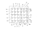
- FIG. 1 is an explanatory plan view showing a schematic configuration of a TFT substrate to be processed by a laser annealing apparatus according to an embodiment of the present invention.
- FIG. 2 is a partial cross-sectional view of a substrate region where a gate line is formed in a TFT substrate.
- FIG. 3 is a schematic block diagram of a laser annealing apparatus according to an embodiment of the present invention.
- FIG. 4 is an explanatory view showing the principle of the laser annealing process of the laser annealing apparatus according to the embodiment of the present invention.
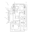
- FIG. 5 is a hardware configuration diagram of the laser annealing apparatus according to the embodiment of the present invention.
- FIG. 6 is an explanatory view showing the behavior according to the film structure of the observation illumination light irradiated to the substrate.
- FIG. 7 is a diagram showing a first reflection spectrum calculated value obtained by fitting the reflection spectrum measurement value measured using the laser annealing apparatus according to the embodiment of the present invention.
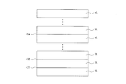
- FIG. 8 is an explanatory view showing a simulation model of the laminated structure of an arbitrary number of films.
- FIG. 9 is a view showing a plurality of reflection spectrum measurement values obtained by performing the laser annealing process with a plurality of laser energy using the laser annealing apparatus of the present invention.
- FIG. 10 is a view showing a second reflection spectrum calculated value obtained by fitting the reflection spectrum measurement value obtained by performing the laser annealing process with the laser energy of 600 mJ / cm 2.
- FIG. 11 is a view showing the relationship between the crystallization level and the electron mobility in polysilicon obtained by performing laser annealing on amorphous silicon.
- FIG. 12 is a flowchart showing the procedure of the laser annealing method.
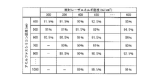
- FIG. 13 is a table showing the relationship between the film thickness of the amorphous silicon film, the irradiation laser energy density, and the crystallization level (%).
- the laser annealing apparatus is used for manufacturing a liquid crystal display or an organic EL display.
- This laser annealing apparatus is a processing apparatus for forming a polysilicon film by irradiating an amorphous silicon film as a semiconductor thin film with a laser beam as an energy beam for annealing to melt and recrystallize it.
- the laser annealing apparatus according to the present embodiment is characterized in that the amorphous silicon film can be selectively irradiated with laser light.
- the area to which the laser annealing apparatus performs the laser annealing process is a semiconductor area to be a channel layer of a TFT provided for each pixel of the TFT substrate.
- the TFT substrate is a substrate on which a pixel electrode, a TFT or the like in a liquid crystal display is formed.
- the TFT substrate is a processing target or a processing target of the crystallization monitoring method, the laser annealing apparatus, and the laser annealing method according to the present embodiment.
- FIG. 1 is a plan view of a TFT substrate
- FIG. 2 is a partial cross-sectional view of a substrate region where gate lines are formed.
- a plurality of gate lines (including a gate electrode pattern portion) 102 and a plurality of data lines 103 are formed in a grid shape intersecting each other on a glass substrate 101. ing. In the vicinity of the intersection between the gate line 102 and the data line 103, there is a TFT formation region 104 in which a TFT as a switching element (driving element) is formed.
- the TFT substrate 100 to be processed by the laser annealing apparatus of this embodiment is in a state before the data lines 103 and the source and drain electrodes (not shown) are formed, and the uppermost layer is the amorphous silicon film 106. .
- the laser annealing process performed on such a TFT substrate 100 is performed on the amorphous silicon film 106 which is the uppermost film of the laminated structure.
- a plurality of gate lines 102 which are parallel to each other are formed on a glass substrate 101.
- the gate insulating film 105 is formed on the glass substrate 101 on which the gate line 102 is formed, and the amorphous silicon film 106 is formed thereon.
- a laser beam is selectively applied to a processing region 104A designed to form a semiconductor region to be a channel layer of the TFT formation region 104 in the plane of the amorphous silicon film 106. Annealing is performed.
- the laser annealing apparatus 1 includes a substrate stage 2, a microlens array stage 3, a laser annealing unit 4, and a crystallization monitor 5 as an observation unit. And a control unit 6.
- the substrate stage 2 is provided with a transfer device (not shown) which mounts the TFT substrate 100 and moves it at a predetermined pitch along the scanning direction S (indicated by an arrow).
- a substrate position observation camera 35 for detecting the position of the TFT substrate 100 is disposed below the substrate stage 2.
- the uppermost layer of the TFT substrate 100 to be processed in the present embodiment is the amorphous silicon film 106, and the state before the data line 103 (see FIG. 1) and the source and drain electrodes (not shown) are formed. It is a substrate. Further, as shown in FIG. 1, in the present embodiment, the scanning direction S of the TFT substrate 100 and the data line 103 are set to be orthogonal to each other.
- the laser annealing unit 4 includes a laser irradiation unit 7, an attenuator 8, an illumination optical system 9, a mask 10, and a microlens array 11.
- the laser annealing unit 4 is provided on the microlens array stage 3 fixed above the substrate stage 2.
- the laser annealing unit 4 is configured to have a plurality of laser beams La along a direction perpendicular to the scanning direction S with respect to the TFT substrate 100 disposed on the substrate stage 2 (see FIG. 4). ) Is configured to irradiate.
- the pitch of the plurality of laser beams La is the same as the pitch of the processing regions 104A disposed along the direction perpendicular to the scanning direction S of the TFT substrate 100.
- the pitch of the laser light La may be set to a pitch that is an integral multiple of 2 or more of the pitch of the processing regions 104A aligned in a direction perpendicular to the scanning direction S of the TFT substrate 100.
- the number of laser beams L to be finally applied to the TFT substrate 100 and the pitch can be set by changing the configuration of the laser light source 12, the illumination optical system 9, the mask 10, the microlens array 11, and the like. .
- the laser irradiation part 7 shown in FIG. 3 is equipped with the laser light source 12 of the number which obtains the said multiple laser beam La finally.
- the laser light source 12 emits the laser light L at the set pulse frequency.
- the attenuator 8 has a function of appropriately attenuating and adjusting the laser light L emitted from the laser light source 12.
- the illumination optical system 9 includes a beam homogenizer 13 and mirrors 14, 15, 16 and the like.
- the mask 10 and the microlens array 11 will be briefly described.
- the mask 10 and the microlens array 11 are provided on the microlens array stage 3.
- a plurality of openings 10A are formed along a direction perpendicular to the scanning direction S of the TFT substrate 100 with respect to the substrate stage 2.
- the microlens array 11 includes a plurality of microlenses 11A.
- the respective micro lenses 11A are arranged corresponding to the respective openings 10A of the mask 10. That is, the mask 10 and the microlens array 11 are arranged to extend in a direction perpendicular to the scanning direction S of the TFT substrate 100 in the substrate stage 2.
- the openings 10A and the microlenses 11A are drawn one by one along the scanning direction S, but as is well known, a plurality of the openings 10A and the microlenses 11A are along the scanning direction S. It is arranged. That is, the openings 10A of the mask 10 are two-dimensionally arranged in a matrix.
- the microlenses 11A of the microlens array 11 are also arranged in a two-dimensional matrix.
- each of the microlenses 11 A of the microlens array 11 is set so as to condense the laser light La toward the processing region 104 A in the TFT formation region 104 of the TFT substrate 100.
- the laser light La collected by the microlens array 11 is selectively irradiated to the processing regions 104A arranged in plural on the TFT substrate 100.
- the laser annealing process can be performed by irradiating the processing region 104A of the TFT 104 on the TFT substrate 100 with the laser light La by the laser annealing processing unit 4. Specifically, the laser annealing process may be sequentially performed by moving the TFT substrate 100 on the substrate stage 2 in the scanning direction S at the pitch of the processing region 104A disposed along the scanning direction S in the TFT substrate 100. .
- Crystallization monitor Next, the configuration of the crystallization monitor 5 will be described. As shown in FIG. 3, the crystallization monitor 5 is provided on the microlens array stage 3.
- the crystallization monitor 5 includes a processing area 104A on the TFT substrate 100 to which the laser light La is irradiated, and a non-processing area (area of amorphous silicon film) close to the processing area 104A and not irradiated with the laser light La. 104B is also provided to be observable.
- an area indicated by an alternate long and short dash line drawn along a direction perpendicular to the scan direction S indicates an observation area M observed by the crystallization monitor 5.
- the observation area M is an elongated area along a direction perpendicular to the scanning direction S of the TFT substrate 100.
- the measurement of the reflected light Lm actually measures the reflected light Lm reflected by the first measurement position 104Bm disposed in the non-processing area 104B and the second measurement position 104Am in the processing area 104A.
- the first measurement positions 104Bm are positions adjacent to the respective processing areas 104A in the non-processing area 104B (longitudinal direction in the figure: approaching in a direction perpendicular to the scanning direction S).
- the second measurement positions 104Am are positions inside the respective processing regions 104A irradiated with the laser light La.
- the crystallization monitor 5 includes an observation light source 17, a microscope 18, an objective lens 19, a spectral camera 20, an observation camera 21, a Z-axis direction drive unit 22, and a controller 23. Is equipped.
- the observation light source 17 is a light source that emits observation illumination light Ls in the visible light range to the observation area M described above.
- the observation illumination light Ls is introduced into the barrel of the microscope 18, passes through the objective lens 19 along the optical axis, and is applied to the surface (the processing area 104A and the non-processing area 104B) of the TFT substrate 100.
- the observation illumination light Ls applied to the surface of the TFT substrate 100 is designed to provide line illumination along the observation area M.
- the reflected light Lm reflected by the surface of the TFT substrate 100 is incident on the microscope 18 from the objective lens 19 and measured by the spectral camera 20.
- the reflected light Lm from the surface of the TFT substrate 100 is a linear reflected light, similarly to the observation illumination light Ls.
- the spectroscope camera 20 reflects the reflected light Lm on such a line from the second measurement position 104Am of each processing area 104A and the reflection from the first measurement position 104Bm of the non-processing area 104B close to each processing area 104A. It is configured in a line camera shape so as to measure the light Lm.
- the spectral camera 20 separates and measures the reflected light Lm, and detects a reflected spectral spectrum as two-dimensional planar data.
- the observation camera 21 acquires two-dimensional planar reflection spectrum data detected by the spectrum camera 20 and outputs the reflection spectrum data to the control unit 6 side.
- control unit 6 includes personal computer (hereinafter referred to as PC) 24 as an arithmetic device, trigger substrate 25, image processing substrate 26, stage control unit 27, and sequencer 28. ing.
- PC personal computer
- the PC 24 is used in the present embodiment, the present invention is not limited to this, and another arithmetic device may be used.
- the PC 24 includes an image board 29.
- the PC 24 is connected to the observation light source 17, the spectroscopic camera 20, the observation camera 21, the controller 23, the trigger substrate 25, and the sequencer 28 (see FIG. 3).
- the sequencer 28 stores a film thickness calculation processing program of each constituent film in the non-processing area 104B and a crystallization level calculation processing program in the processing area 104A.
- the crystallization level (A) is defined as the content ratio (%) of polysilicon when amorphous silicon and polysilicon are mixed in the film.
- the film thickness calculation processing program and the crystallization level calculation processing program are stored in the sequencer 28 in the present embodiment, they may be stored in the PC 24.
- the trigger substrate 25 includes a branch circuit 32 and a timing control circuit 33. As shown in FIG. 3, the trigger substrate 25 is connected to the laser irradiation unit 7, the PC 24, the image processing substrate 26, and the sequencer 28.
- the image processing substrate 26 is incorporated in the annealing control device 34. As shown in FIG. 3, the image processing substrate 26 is connected to the substrate position observation camera 35, the laser irradiation unit 7, and the trigger substrate 25. The image processing substrate 26 acquires positional information of the TFT substrate 100 from the substrate position observation camera 35. The image processing board 26 outputs a shot trigger signal to the trigger board 25.
- the branch circuit 32 of the trigger substrate 25 outputs the shot trigger signal output from the image processing substrate 26 to the laser irradiation unit 7.
- the laser irradiation unit 7 drives the laser light source 12 based on the shot trigger signal to emit the laser light L with predetermined irradiation laser energy.
- the timing control circuit 33 of the trigger substrate 25 outputs the trigger signal to the image board 29 of the PC when the trigger shot signal from the image processing substrate 26 is input through the branch circuit 32.
- the PC 24 When the trigger signal is input to the image board 29, the PC 24 outputs a drive signal to the observation light source 17, the spectroscopic camera 20, the observation camera 21, the controller 23, and the like.
- the controller 23 performs drive control of the Z-axis direction drive unit 22.
- the PC 24 takes in two-dimensional planar data of the reflection spectrum obtained by the spectral camera 20 from the observation camera 21 to the image board 29 at the timing when the trigger signal is output.
- the stage control unit 27 is connected to the sequencer 28 and a transport device (not shown) of the substrate stage 2.
- the stage control unit 27 controls the movement of the TFT substrate 100 in the scan direction S by driving a transfer device (not shown).
- the film thickness calculation processing program is calculated from the film structure data by inputting the film structure data including the number of films of the laminated structure, the material, the set film thickness and refractive index of each component film, and the extinction coefficient to the sequencer 28.
- the calculated first reflection spectrum calculation value is calculated.
- the film thickness calculation processing program is configured to measure the first reflection spectrum measured value obtained from the first measurement position 104Bm of the non-processing area 104B input from the observation camera 21 to the image board 29 and the first measurement position 104Bm. Fitting of the first reflection spectral spectrum calculation value is performed to calculate a film thickness calculation value of each constituent film of the first measurement position 104Bm close to the predetermined processing region 104A.
- the crystallization level calculation processing program calculates a second reflection spectral spectrum calculation value from the film structure data and the thickness calculation value of each component film calculated by the film thickness calculation processing program. Then, the crystallization level calculation processing program is configured to measure the second reflection spectrum measured value obtained from the processing area 104A (the second measurement position 104Am) input from the observation camera 21 to the image board 29, and the second reflection spectrum Fitting of the calculated value is performed to calculate the crystallization level (A) in the processing region 104A.
- the calculation method performed by the crystallization monitoring method described later is written as software.
- the plurality of processing regions 104A in the amorphous silicon film 106 are melted and recrystallized, the plurality of processing regions 104A and the plurality of processing regions 104A are adjacent to each other.
- the illumination light Ls for observation is irradiated to the non-processing area 104B, the reflected light Lm is measured by the spectral camera 20, and the reflection spectral measurement value is two-dimensionally acquired in a two-dimensional manner.
- the first reflection spectrum calculated value using information on the film structure of the TFT substrate 100 (the number of films in the laminated structure, the material, the designed film thickness, the refractive index of each component layer, and the extinction coefficient) (Calculating value of first spectral spectrum) is calculated.
- a first reflection spectrum measurement value (first value) which is an actual measurement value acquired in the non-processing area 104B adjacent to the specific processing area 104A.
- the calculated film thickness in the non-processing region 104B is calculated.
- the processing area 104A irradiated with the laser light L is irradiated with the observation illumination light Ls and reflected light reflected by the processing area 104A
- Second reflection spectrum spectrum calculation value (second spectrum spectrum calculation value calculated from the second reflection spectrum measurement value (second spectrum measurement value) obtained by measurement and the film structure data and the obtained film thickness calculation value
- the degree of crystallization (A) of the processing area 104A at this position is calculated by the fitting of
- the crystallization level (A) is, as described above, the content ratio (%) of polysilicon when amorphous silicon and polysilicon are mixed in the film.
- the crystallization level (A) is proportional to the electron mobility which is the electrical performance of the TFT 104.
- the laser annealing apparatus 1 is an apparatus using the above-described crystallization monitoring method, and therefore can calculate the crystallization level (A) immediately after the laser annealing process in real time. For this reason, in the laser annealing apparatus 1, feedback control can be performed based on the calculated crystallization level (A).
- the laser annealing processing unit 4 emits light to the TFT substrate 100 to be subjected to the laser annealing processing next based on the crystallization level (A) after the previous laser annealing processing.
- the laser energy of the laser light L can be adjusted to perform the laser annealing process.
- the laser irradiation density and the number of pulses may be adjusted.
- the reflected light Lm from the amorphous silicon film 106 in the non-processing region 104B close to the processing region 104A is measured by the crystallization monitor 5 in order to obtain the first reflection spectrum measurement value.
- the reflected light Lm from the polysilicon film 107 (see FIG. 6) in the processing region 104A is measured by the crystallization monitor 5 in order to obtain the second reflection spectrum measurement value. Then, the reflection spectrum measurement value including the measured first reflection spectrum measurement value and the second reflection spectrum measurement value is detected as two-dimensional planar data.
- FIG. 6 shows a laminated structure formed of a gate line (gate electrode) 102, a gate insulating film 105, and a polysilicon film 107 sequentially formed on a glass substrate (see FIG. 1).
- FIG. 6 shows the observation illumination light Ls incident toward the surface of the polysilicon film 107 and the reflected light Lm thereof. The observation illumination light Ls is incident on the surface of the polysilicon film 107 perpendicularly.
- the light incident on the polysilicon film 107 is reflected by the surface of the polysilicon film 107, the interface between the polysilicon film 107 and the gate insulating film 105, the interface between the gate line 102 and the gate insulating film 105, etc. ) Is set to be incident on the crystallization monitor 5 as Lm.
- the reflected light Lm incident on the crystallization monitor 5 is measured by the spectroscopic camera 20, and the reflection spectrum measurement value is two-dimensionally acquired in a two-dimensional manner as described above.
- the gate line (gate electrode) 102 is a material with high light reflectance, such as titanium nitride (TiN), which has high light reflectance, reflection obtained by reflection of the observation illumination light Ls
- the light Lm is mainly reflected light unique to the stacked structure of the gate insulating film 105 and the polysilicon film 107.
- FIG. 7 is a waveform of a simulation obtained by performing fitting in a fitting wavelength range of, for example, 430 nm to 700 nm with respect to a measured value of a reflection spectrum of the polysilicon film 107 obtained by recrystallization after laser annealing.
- FIG. 8 is a simulation model of the laminated structure, showing that the constituent films 1L, 2L, 3L..., AL, bL..., OL are sequentially laminated from the lowermost layer in the laminated structure of the material film. There is. As shown in FIG. 8, the reflectances at the interfaces between the constituent films bonded to each other in the upper and lower directions are r21, r32, and rba.
- the refractive index, extinction coefficient and film thickness of each of the constituent films oL to 1L shown in FIG. 8 can be expressed as follows.
- Component film-aL (Refractive index, extinction coefficient, film thickness) (na, ka, da)
- component film-3L (refractive index, extinction coefficient, film thickness) (n3, k3, d3)
- component film-2L (refractive index, Extinction coefficient, film thickness) (n2, k2, d2)
- component film-1L (refractive index, extinction coefficient, film thickness) (n1, k1, d1)
- the complex refractive index of each of the constituent films bL to 1L can be expressed as follows.
- the following i is an imaginary unit.
- Complex refractive index Na of the constituting film-aL Na na-ka * i of the constituting film-3 L
- Complex refractive index of the N3 n3-k3 * i constituting film-2L
- Complex refractive index N2 n2-k2 * i
- ⁇ calculation is performed on each of the constituent films for each measurement wavelength ⁇ .
- r of a plurality of layers is calculated sequentially as shown in the following equation.
- r (cba) ⁇ rcb + rba * exp (-2i * ⁇ b) ⁇ / ⁇ 1 + rcb * rba * exp (-2 * ⁇ b) ⁇
- r (dcba) ⁇ rdc + rcba * exp (-2i * ⁇ c) ⁇ / ⁇ 1 + rdc * rcba * exp (-2i * ⁇ c) ⁇
- FIG. 9 shows a reflection spectrum of the polysilicon film 107 after the laser annealing process for each irradiation energy density as the laser energy.
- the laser uses a KrF excimer laser.
- FIG. 10 performs fitting on the reflection spectrum measurement value (second reflection spectrum measurement value) when the laser annealing process is performed at, for example, the irradiation energy density of 600 mJ / cm 2 among the reflection spectrum measurement values shown in FIG. 9 An example is shown.
- the reflection spectrum measured value when the irradiation energy density is 600 mJ / cm 2 and the calculated film thickness value of each component film in the non-processing region 104B (first measurement position 104Bm) obtained by the above calculation.
- a reflection spectrum calculation value (second reflection spectrum calculation value) calculated from the film structure data. This fitting makes it possible to unambiguously calculate the crystallization level (A).
- the calculation method of the crystallization level (A) is as follows. The following calculation is performed at each measurement wavelength ⁇ with respect to the reflection spectrum measured value (integrated spectrum).
- the complex dielectric constant of amorphous silicon and single crystal silicon is calculated by the following equation.
- the complex dielectric constant ⁇ of polysilicon of the constituent film is calculated.
- NSi ⁇ 0.5
- the reflectance is calculated in the same manner as the above-described calculation for film thickness fitting. At this time, the film thickness calculation value obtained as a result of the film thickness fitting described above is substituted for the film thickness of each constituent film.
- npoly-Si na-Si ⁇ A + nc-Si ⁇ (1-A) (1)
- kpoly-Si ka-Si ⁇ A + kc-Si ⁇ (1-A) (2)
- na-Si is the refractive index of amorphous silicon
- nc-Si is the refractive index of single crystal silicon
- ka-Si is the extinction coefficient of amorphous silicon
- kc-Si is the extinction coefficient of single crystal silicon
- A is a-Si It is the above-mentioned crystallization level represented by the ratio of / poly-Si. Therefore, the crystallization level (A) in each of the formulas (1) and (2) can be calculated.
- the crystallization level (A) of this polysilicon film 107 is calculated to be 96.9%, for example.
- the FIG. 11 shows the relationship between the crystallization level (A) and the electron mobility of polysilicon.
- the electron mobility corresponding to the crystallization level (A) of 96.9% obtained by the above calculation was 163 cm 2 / Vs.
- the TFT substrate 100 is disposed on the substrate stage 2, and the laser annealing processing unit 4 performs the laser annealing process at a predetermined irradiation laser energy density.
- the laser light La is selectively emitted to the plurality of processing regions 104A aligned in a line in a direction perpendicular to the scanning direction S of the TFT substrate 100.
- the amorphous silicon on the top layer of the stacked structure of the TFT substrate 100 is selectively recrystallized to polysilicon.
- the crystallization monitor 5 is driven to set the second measurement positions 104Am and the first measurement positions 104Am, which are set along a direction perpendicular to the scan direction S of the TFT substrate 100.
- the reflected light Lm from the measurement position 104Bm is measured by the spectral camera 20.
- the reflection spectrum detected by the spectral camera 20 is detected by the observation camera 21 as two-dimensional planar data. Two-dimensional planar data detected by the observation camera 21 is taken into the image board 29 of the PC 24.
- the sequencer 28 takes in the above two-dimensional planar reflection spectrum data from the PC 24 and uses the film thickness calculation processing program and the crystallization level calculation processing program to set the processing area 104A disposed at each position on the substrate position coordinates.
- the crystallization level (A) is calculated.
- the sequencer 28 is provided with a table as shown in FIG. 13, and this table is obtained by comparing the target crystallization level with the crystallization level (A) obtained by calculation. By reference, control is performed to change the laser energy of the TFT substrate 100 next time.
- the film thickness obtained by the film thickness calculation processing program was 600 nm
- the crystallization level (A) calculated by the crystallization level calculation processing program was 90.5%
- the target crystallization level was 94%.
- the irradiation laser energy density is changed on the recipe of the sequencer 28 so as to be 600 mJ / cm 2 .
- the irradiation laser energy density thus changed is reflected in the next laser annealing process of the TFT substrate 100.
- FIG. 12 is a flowchart showing the main part of the laser annealing method according to the embodiment of the present invention.
- the laser annealing method according to the present embodiment will be described by applying to the above-described laser annealing apparatus 1.
- step S1 data of the film structure of the TFT substrate 100 which is an annealing treated substrate is input (step S1).
- step S2 the laser annealing process is performed on the processing area 104A on the TFT substrate 100, and simultaneously, as shown in FIG. 1, reflections at all the first measurement positions 104Bm and the second measurement positions 104Am in the observation area M Spectral spectrum data is acquired (step S2).
- the film thickness of each constituent film is calculated by fitting with the calculated first reflection spectral spectrum calculated value (step S3).
- the film structure data includes the number of films in the laminated structure, the material, the designed film thickness, and the refractive index and extinction coefficient of each component film.
- a second reflection spectrum measurement value of the second measurement position 104Am of the processing area 104A subjected to the laser annealing, a second calculated from the film structure data, and the film thickness of each component film obtained in step S3 The crystallization level is calculated by fitting the reflection spectrum calculation value (step S4).
- step S5 it is determined whether the difference between the crystallization level obtained by comparing the crystallization level obtained in step S4 with the target crystallization level and the target crystallization level is within an error range (step S5).
- step S5 when the difference between the obtained crystallization level and the target crystallization level is within the error range (less than or equal to), it is determined that the laser annealing condition of the substrate position coordinates for which the crystallization level is calculated is not changed. (Step S6).
- the following adjustment process is performed. That is, when the difference between the crystallization level and the target crystallization level is equal to or more than the error range, the irradiation laser energy density of the substrate position coordinates measured by the irradiation laser energy density or the look-up table of the number of pulses and the crystallization level Alternatively, the number of times of irradiation is changed and recorded on the recipe of the sequencer 28 (step S7). The irradiation laser energy density or the number of irradiations recorded in this way is reflected in the next laser annealing process.
- the illumination light Ls for observation is simultaneously irradiated to the non-processing area 104B and the processing area 104A, and the first reflection spectrum measurement value and the second reflection spectrum measurement value are respectively measured.
- the first reflection spectrum measurement value and the second reflection spectrum measurement value are respectively measured.
- step S7 which is an adjustment process, in the TFT substrate 100 to be subjected to the next laser annealing process, with respect to the processing area 104A at the same coordinates as the processing area 104A for which the crystallization level was obtained in the previous processing , Adjust the laser energy.
- step S7 which is an adjustment process, in the TFT substrate 100 to be subjected to the next laser annealing process, with respect to the processing area 104A at the same coordinates as the processing area 104A for which the crystallization level was obtained in the previous processing .
- the laser annealing apparatus 1 of the present embodiment it is possible to immediately calculate the crystallization state of polysilicon crystallized immediately after the laser annealing process on amorphous silicon. By grasping this crystallization level, it is possible to grasp the electrical characteristics of the produced polysilicon. Therefore, it is possible to prevent the occurrence of a defect in the result of the next laser annealing process. Therefore, according to the laser annealing apparatus 1 according to the present embodiment, the yield in the manufacturing process of the TFT substrate 100 can be greatly improved.
- the first reflection spectrum measurement value and the second reflection spectrum measurement value correspond to the substrate position coordinates of the non-processing region 104B and the processing region 104A respectively measured.
- the electron mobility of the processing region 104A is uniform in the substrate surface in the next TFT substrate 100. It is possible to That is, even when the film structure in the substrate surface has a distribution as the screen becomes larger, the electron mobility of the TFT substrate 100 in the same lot can be made uniform. Therefore, the display performance of the liquid crystal display provided with the TFT substrate 100 manufactured by the laser annealing device 1 can be improved.
- the plurality of processing regions 104A forming a line in the direction perpendicular to the scan direction S of the TFT substrate 100 are simultaneously subjected to the laser annealing process, but along the direction perpendicular to the scan direction S
- the laser annealing process may be performed intermittently at a pitch that is an integral multiple of twice or more the pitch of the processing region 104A.
- the processing areas 104A and all non-processing areas 104B in the vicinity of the respective processing areas 104A are reflected.
- the light Lm is measured.
- the reflected light Lm may be measured only at important points without measuring the reflected light Lm in all the processing regions 104A and the non-processing region 104B in the vicinity thereof.
- the crystallization monitoring method is described by applying the laser annealing apparatus 1 and the laser annealing method, but an annealing apparatus such as a lamp annealing that does not use an energy beam for annealing and a laser beam, an annealing method Of course, the present crystallization monitoring method may be applied.
- the material film is not limited to these.
- the laser annealing processing unit 4 and the crystallization monitor 5 are simultaneously driven to perform irradiation of the laser light La and irradiation of the observation illumination light Ls simultaneously.
- the irradiation of the observation illumination light Ls may be later than the irradiation of the laser light La.
- the reflected light Lm was measured as the emitted light emitted from the semiconductor thin film, but the transmitted light transmitted through the TFT substrate 100 by irradiating the observation illumination light Ls from below the substrate stage 2 May be measured by the crystallization monitor 5.
- the crystallization monitor 5 For example, in the case of manufacturing a top gate structure (staggered type) as a TFT, an amorphous silicon film may be formed on a glass substrate. Therefore, observation illumination light is applied from below the glass substrate to transmit it. The light may be measured by the crystallization monitor 5.
- the openings 10A of the mask 10 are arranged in one row in a direction perpendicular to the scanning direction S of the TFT substrate 100, but even if a plurality of rows are provided. Good.
- the rows of the microlenses 11A of the microlens array 11 may be plural.
- the setting value of the next laser energy may be determined by comparing the obtained crystallization level (A) with the target crystallization level, or the next laser energy Control may be performed to adjust the increase or decrease without obtaining the set value of.
Landscapes
- Engineering & Computer Science (AREA)
- Physics & Mathematics (AREA)
- Optics & Photonics (AREA)
- Plasma & Fusion (AREA)
- Mechanical Engineering (AREA)
- Recrystallisation Techniques (AREA)
- Electromagnetism (AREA)
Abstract
アニールを行う処理領域に近接するレーザ光が照射されない非処理領域の積層構造の各構成膜の膜厚計算値を算出し、処理領域の第2分光スペクトル測定値と、膜厚計算値から計算される第2分光スペクトル計算値と、のフィッティングにより、処理領域の結晶化レベルを算出して、次回にレーザアニール処理を行うTFT基板に対して照射するレーザ光のレーザエネルギーを調整する。
Description
本発明は、レーザアニール処理を施した半導体薄膜の電気的特性を把握することを可能とする結晶化モニタ方法、この結晶化モニタ方法を用いたレーザアニール装置ならびにレーザアニール方法に関する。
近年、液晶ディスプレイ、有機ELディスプレイなどの表示装置では、基板の大型化が進み、駆動素子としての薄膜トランジスタ(以下、TFTという)の高性能化が求められている。TFTのチャネル層としては、アモルファスシリコンよりも電子移動度の高いポリシリコンが用いられている。このポリシリコンの作製には、レーザアニール法が用いられる。このレーザアニール法は、アモルファスシリコンにレーザ光を照射し、レーザ光を吸収して溶融したシリコンが急速に冷却されて再結晶化することにより、アモルファスシリコンをポリシリコンに変化させる方法である。
このレーザアニール法によって作製されたポリシリコンは、照射するレーザ光のエネルギー量やアモルファスシリコン膜の膜厚などによって結晶化の度合いが大きく左右される。ポリシリコンは、結晶化の度合いに応じて電気特性が変わる。したがって、基板上に成膜したアモルファスシリコンが適正にポリシリコンに再結晶化しているか否かを知るために、ポリシリコンの結晶状態を観察する必要がある。また、基板面内のアモルファスシリコン膜に膜厚分布が存在していても、基板面内で均一な電気特性を有するポリシリコン膜を得ることが望まれている。
現在、レーザアニール処理されて作製されたポリシリコンの状態を観察する方法としては、以下の3つがある。まず第1の方法は、レーザアニール処理を施した膜表面全体の状態を目視により観察する、所謂マクロ観察と称される方法である。第2の方法は、電子顕微鏡などの分析装置にて観察する方法である。第3の方法は、TFTの作製が完了した時点で、TFTの電気的特性を測定することにより、ポリシリコンの電子移動度を測る方法である。
上記の第1の方法では、定量的な観察結果を得ることができず、明らかな構造欠陥の有無や、膜表面の色の差異や色ムラを把握する程度のことしかできない。第2の方法は、被観察物である試料の作製などに長い時間がかかってしまう。第3の方法は、レーザアニール処理の後にTFTが構築されるまでに多くの製造工程を施す必要があるため、レーザアニール処理から測定までに長い時間がかかってしまう。このように、第2の方法および第3の方法では、レーザアニール処理時には結晶の状態を確認できない。このため、表示装置の製造工程では、ポリシリコンの電子移動度に不具合があったとしても、不具合が確認されるまでに長時間を要してしまう。このため、測定結果を得るまでの間に、電子移動度に不具合を備えた製品(基板)が大量に発生してしまう。
近年、測定結果を得るまでに長時間を要せずにレーザアニール処理後の結晶状態を確認する評価方法が提案されている(特許文献1参照)。この評価方法では、ポリシリコン膜の光の透過率を測定してその透過率から結晶化した薄膜の評価を行う。他の方法として、レーザアニール処理が施された領域からの反射光の分光特性によってレーザアニール処理が適正になされたか否かを確認する方法が提案されている(特許文献2参照)。
しかしながら、ポリシリコン膜を透過した光の透過率や、ポリシリコン膜の表面で反射した光の分光特性などを観察することによって、レーザアニール処理が適正に行われたか否かを精度良く判定することは困難であった。例えば、液晶ディスプレイの製造工程では、ガラス基板上にゲートラインを形成し、その上にゲート絶縁膜、アモルファスシリコン膜を順次積層する。レーザアニール処理を施すときには、アモルファスシリコン膜の下に複数の膜が存在する。したがって、ポリシリコン膜を透過した光や、ポリシリコン膜からの反射光は、ポリシリコン膜直下の複数の膜やそれぞれの界面からの影響を受けるため、レーザアニール処理が適正に行われたか否かを精度良く判定することは困難であった。
本発明は、上記の課題に鑑みてなされたものであって、レーザアニール処理直後の半導体薄膜の結晶化状態を即時に算出可能にし、半導体薄膜の電気的特性を把握することを可能にし、レーザアニール処理の不具合を短時間で解消可能とする、結晶化モニタ方法、レーザアニール装置、およびレーザアニール方法を提供することを目的とする。
上述した課題を解決し、目的を達成するために、本発明の態様は、アニール用エネルギービームを、基板上に形成された積層構造の最上層に配置された半導体薄膜の処理領域に照射して、当該処理領域を結晶化させるアニール処理に伴い、観察用照明光を前記半導体薄膜に照射して当該半導体薄膜から出る出射光を測定することより、前記処理領域の結晶化レベルを観察する結晶化モニタ方法であって、前記処理領域に近接する、アニール用エネルギービームが照射されない非処理領域に、観察用照明光を照射して当該非処理領域から出る出射光を計測して検出した第1分光スペクトル測定値と、前記積層構造の膜構造データから計算される第1分光スペクトル計算値と、のフィッティングにより、前記積層構造の各構成膜の膜厚計算値を算出し、アニール用エネルギービームが照射された前記処理領域に、観察用照明光を照射して当該処理領域から出る出射光を計測して検出した第2分光スペクトル測定値と、上記膜構造データおよび前記膜厚計算値から計算される第2分光スペクトル計算値と、のフィッティングにより、前記処理領域の結晶化レベルを算出することを特徴とする。
上記態様としては、前記膜構造データは、膜数、材料、設計膜厚、構成膜の屈折率、および消衰係数であることが好ましい。
上記態様としては、前記処理領域と前記非処理領域とに同時に観察用照明光を照射して、前記第1分光スペクトル測定値および前記第2分光スペクトル測定値を、それぞれを測定した前記非処理領域および前記処理領域の基板位置座標と対応するように2次元平面的なデータとして検出することが好ましい。
本発明の他の態様は、レーザアニール装置であって、アニール用のレーザ光を出射するレーザ光源と、前記レーザ光源から出射されたレーザ光を、基板上に形成された積層構造の最上層に配置された半導体薄膜の処理領域に照射する照明光学系と、を備えるレーザアニール処理部と、観察用照明光を前記半導体薄膜に照射し、当該半導体薄膜から出る出射光を測定して分光スペクトルデータとして検出する観察部と、前記分光スペクトルデータに基づいて前記レーザアニール処理部および前記観察部を制御する制御部と、を備え、前記制御部は、前記処理領域に近接するレーザ光が照射されない非処理領域に、観察用照明光を照射して該非処理領域から出る出射光を測定して検出した第1分光スペクトル測定値と、前記積層構造の膜構造データから計算される第1分光スペクトル計算値と、のフィッティングにより、前記積層構造の各構成膜の膜厚計算値を算出し、レーザ光が照射された前記処理領域に、観察用照明光を照射して当該処理領域から出る出射光を測定して検出した第2分光スペクトル測定値と、前記膜構造データおよび前記膜厚計算値から計算される第2分光スペクトル計算値と、のフィッティングにより、前記処理領域の結晶化レベルを算出し、前記レーザアニール処理部へ、次回にレーザアニール処理を行う基板に対して、前記結晶化レベルに基づいて当該レーザアニール処理部から照射するレーザ光のレーザエネルギーを調整する制御を行うことを特徴とする。
上記態様としては、前記膜構造データは、膜数、材料、設計膜厚、構成膜の屈折率、および消衰係数であることが好ましい。
上記態様としては、前記出射光は、観察用照明光が前記半導体薄膜で反射した反射光であることが好ましい。
上記態様としては、前記観察部は、前記処理領域と前記非処理領域とに同時に観察用照明光を照射して、前記第1分光スペクトル測定値および前記第2分光スペクトル測定値を、それぞれを測定した前記非処理領域および前記処理領域の基板位置座標と対応するように2次元平面的なデータとして検出し、前記制御部は、前記レーザアニール処理部に対して、前記処理領域の基板位置座標と対応する、次回にレーザアニール処理を行う基板の処理領域へ、前記結晶化レベルと目標結晶化レベルとの差に応じて前記レーザアニール処理部から出射するレーザ光のレーザエネルギーを調整する制御を行うことが好ましい。
本発明の他の態様は、レーザアニール方法であって、アニール用のレーザ光源から出射されたレーザ光を、基板上に形成された積層構造の最上層に配置された半導体薄膜の処理領域に照射して前記処理領域を結晶化させるレーザアニール処理工程と、観察用照明光を、前記処理領域と前記処理領域に近接する前記レーザ光が照射されない非処理領域と、に照射して前記基板の表面から出る出射光を測定して検出したそれぞれの分光スペクトルデータを検出する工程と、前記分光スペクトルデータのうち前記非処理領域で得られた第1分光スペクトル測定値と、前記積層構造の膜構造データから計算される第1分光スペクトル計算値と、のフィッティングにより、前記積層構造の各構成膜の膜厚計算値を算出する工程と、前記分光スペクトルデータのうち前記処理領域で得られた第2分光スペクトル測定値と、前記膜構造データおよび前記膜厚計算値から計算される第2分光スペクトル計算値と、のフィッティングにより、前記処理領域の結晶化レベルを算出する工程と、次回のレーザアニール処理を行う基板に対して、前記結晶化レベルに基づいて前記レーザアニール処理工程において照射するレーザ光のレーザエネルギーを調整する調整工程と、を備えることを特徴とする。
上記態様としては、前記調整工程は、前記結晶化レベルと目標結晶化レベルとの差に応じて前記レーザ光源から照射するレーザ光のレーザエネルギーを調整することが好ましい。
上記態様としては、前記非処理領域と前記処理領域とに同時に観察用照明光を照射して、前記第1分光スペクトル測定値および前記第2分光スペクトル測定値を、それぞれを測定した前記非処理領域および前記処理領域の基板位置座標と対応するように2次元平面的なデータとして検出し、前記調整工程は、次回のレーザアニール処理を行う基板に対して、前記結晶化レベルの算出に用いられる第2分光スペクトル測定値を得た前記処理領域と基板位置座標が対応する処理領域へ、前記レーザ光源から照射するレーザ光のレーザエネルギーを調整することが好ましい。
本発明に係る結晶化モニタ方法、レーザアニール装置、およびレーザアニール方法によれば、レーザアニール(アニール)処理直後の半導体薄膜の結晶化状態を即時に算出可能にし、半導体薄膜の電気的特性を把握することを可能にする。本発明に係るレーザアニール装置およびレーザアニール方法によれば、レーザアニール処理の不具合を短時間で解消することができ、歩留まりを向上させる効果がある。また、本発明によれば、基板面内のアモルファスシリコン膜の膜厚分布が存在した場合でも、基板面内で均一な電気特性を有するポリシリコン膜を得ることを可能にする効果がある。
以下に、本発明の実施の形態に係る結晶化モニタ方法、レーザアニール装置、およびレーザアニール方法の詳細を図面に基づいて説明する。但し、図面は模式的なものであり、各部材の寸法や寸法の比率や形状などは現実のものとは異なり、図面相互間においても構成部の配置位置が異なる部分が含まれている。また、本実施の形態においては、観察用照明光を照射した半導体薄膜からの出射光が、基板面で反射した反射光であるため、計測される分光スペクトルとして反射分光スペクトルという表現を用いる。
本実施の形態に係るレーザアニール装置は、液晶ディスプレイや有機ELディスプレイの製造に用いられる。このレーザアニール装置は、半導体薄膜としてのアモルファスシリコン膜に対して、アニール用エネルギービームとしてのレーザ光を照射して溶融・再結晶化させることでポリシリコン膜を形成する処理装置である。本実施の形態に係るレーザアニール装置は、アモルファスシリコン膜に対して、レーザ光を選択的に照射することができるという特徴がある。
このレーザアニール装置がレーザアニール処理を施す領域は、TFT基板の画素毎に設けられるTFTのチャネル層となる半導体領域である。TFT基板とは、液晶ディスプレイにおける画素電極やTFTなどを形成する基板である。TFT基板は、本実施の形態に係る結晶化モニタ方法、レーザアニール装置、およびレーザアニール方法の処理対象もしくは加工対象となる。
[TFT基板] ここで、本実施の形態の説明に先駆けて、図1および図2を用いてTFT基板について簡単に説明する。図1はTFT基板の平面図、図2はゲート線が形成された基板領域の部分断面図である。
図1に示すように、TFT基板100は、ガラス基板101上に、複数のゲート線(ゲート電極パターン部分を含む)102と、複数のデータ線103と、が互いに交差して格子状に形成されている。ゲート線102とデータ線103との交差部の近傍には、スイッチング素子(駆動素子)としてのTFTを形成するTFT形成領域104がある。なお、本実施の形態のレーザアニール装置で処理を行うTFT基板100は、データ線103や図示しないソース電極およびドレイン電極などが形成される前の状態であり、最上層がアモルファスシリコン膜106である。
このようなTFT基板100に行われるレーザアニール処理は、積層構造の最上膜であるアモルファスシリコン膜106に対して行われる。図1に示すように、ガラス基板101上には、互いに平行をなす複数のゲート線102が形成されている。図2に示すように、ゲート線102が形成されたガラス基板101上には、ゲート絶縁膜105が成膜され、その上にアモルファスシリコン膜106が成膜されている。
図1に示すように、アモルファスシリコン膜106の平面内において、TFT形成領域104のチャネル層となる半導体領域が形成されるように設計された処理領域104Aに対してレーザ光を選択的に照射してアニール処理を行う。
[レーザアニール装置]
次に、本実施の形態に係るレーザアニール装置の構成を説明する。図3に示すように、本発明の実施の形態に係るレーザアニール装置1は、基板ステージ2と、マイクロレンズアレイステージ3と、レーザアニール処理部4と、観察部としての結晶化モニタ5と、制御部6と、を備える。
次に、本実施の形態に係るレーザアニール装置の構成を説明する。図3に示すように、本発明の実施の形態に係るレーザアニール装置1は、基板ステージ2と、マイクロレンズアレイステージ3と、レーザアニール処理部4と、観察部としての結晶化モニタ5と、制御部6と、を備える。
(基板ステージ)
図3に示すように、基板ステージ2は、TFT基板100を載せてスキャン方向S(矢印で示す)に沿って所定のピッチで移動させる、図示しない搬送装置を備えている。この基板ステージ2の下方には、TFT基板100の位置検出を行う基板位置観察カメラ35が配置されている。
図3に示すように、基板ステージ2は、TFT基板100を載せてスキャン方向S(矢印で示す)に沿って所定のピッチで移動させる、図示しない搬送装置を備えている。この基板ステージ2の下方には、TFT基板100の位置検出を行う基板位置観察カメラ35が配置されている。
なお、本実施の形態において処理を行うTFT基板100は、最上層がアモルファスシリコン膜106であり、データ線103(図1参照)や図示しないソース電極およびドレイン電極などが形成される前の状態の基板である。また、図1に示すように、本実施の形態では、TFT基板100のスキャン方向Sと、データ線103と、が直交するように設定されている。
(レーザアニール処理部)
レーザアニール処理部4は、レーザ照射部7と、アッテネータ8と、照明光学系9と、マスク10と、マイクロレンズアレイ11と、を備えている。このレーザアニール処理部4は、基板ステージ2の上方に固定されたマイクロレンズアレイステージ3に設けられている。
レーザアニール処理部4は、レーザ照射部7と、アッテネータ8と、照明光学系9と、マスク10と、マイクロレンズアレイ11と、を備えている。このレーザアニール処理部4は、基板ステージ2の上方に固定されたマイクロレンズアレイステージ3に設けられている。
本実施の形態では、レーザアニール処理部4は、基板ステージ2上に配置したTFT基板100に対して、スキャン方向Sに対して直角をなす方向に沿って複数本のレーザ光La(図4参照)を照射するように構成されている。なお、複数本のレーザ光Laのピッチは、TFT基板100のスキャン方向Sに直角をなす方向に沿って配置される処理領域104Aのピッチと同じである。なお、レーザ光Laの上記ピッチは、TFT基板100のスキャン方向Sに直角をなす方向に沿って列をなす処理領域104Aのピッチの2以上の整数倍のピッチに設定してもよい。なお、最終的にTFT基板100に照射するレーザ光Lの本数ならびに上記ピッチは、レーザ光源12、照明光学系9、マスク10およびマイクロレンズアレイ11などの構成を変更することにより設定することができる。
図3に示すレーザ照射部7は、最終的に上記複数本のレーザ光Laを得る数のレーザ光源12を備えている。レーザ光源12は、設定されたパルス周波数でレーザ光Lを出射する。アッテネータ8は、レーザ光源12から出射されたレーザ光Lを適切に減衰して調整する機能を備える。照明光学系9は、ビームホモジナイザ13やミラー14,15,16などを備えている。
ここで、マスク10とマイクロレンズアレイ11について簡単に説明する。マスク10とマイクロレンズアレイ11は、マイクロレンズアレイステージ3に設けられている。マスク10は、基板ステージ2に対して、TFT基板100のスキャン方向Sに直角をなす方向に沿って複数の開口部10Aが形成されている。
マイクロレンズアレイ11は、複数のマイクロレンズ11Aを備える。それぞれのマイクロレンズ11Aは、マスク10のそれぞれの開口部10Aに対応して配置されている。
すなわち、マスク10およびマイクロレンズアレイ11は、基板ステージ2におけるTFT基板100のスキャン方向Sに対して直角をなす方向に沿って細長く延びるように配置されている。なお、図4では、開口部10Aとマイクロレンズ11Aをスキャン方向Sに沿ってそれぞれ1つずつ描いているが、周知のように、開口部10Aおよびマイクロレンズ11Aはスキャン方向Sに沿って複数が配置されている。すなわち、マスク10の開口部10Aは、2次元的にマトリクス状に配置されている。これに対応して、マイクロレンズアレイ11のマイクロレンズ11Aも2次元的にマトリクス状に配置されている。
すなわち、マスク10およびマイクロレンズアレイ11は、基板ステージ2におけるTFT基板100のスキャン方向Sに対して直角をなす方向に沿って細長く延びるように配置されている。なお、図4では、開口部10Aとマイクロレンズ11Aをスキャン方向Sに沿ってそれぞれ1つずつ描いているが、周知のように、開口部10Aおよびマイクロレンズ11Aはスキャン方向Sに沿って複数が配置されている。すなわち、マスク10の開口部10Aは、2次元的にマトリクス状に配置されている。これに対応して、マイクロレンズアレイ11のマイクロレンズ11Aも2次元的にマトリクス状に配置されている。
図4に示すように、マイクロレンズアレイ11の各マイクロレンズ11Aは、それぞれがTFT基板100におけるTFT形成領域104内の処理領域104Aに向けてレーザ光Laを集光し得るように設定されている。マイクロレンズアレイ11によって、集光されたレーザ光Laは、TFT基板100上に複数配列される処理領域104Aに選択的に照射される。本実施の形態のような構成により、レーザアニール処理を必要としない領域を無駄に結晶化させることを回避できる。
レーザアニール処理部4により、TFT基板100上のTFT104の処理領域104Aに対してレーザ光Laを照射してレーザアニール処理を行うことができる。具体的には、基板ステージ2上のTFT基板100を、TFT基板100におけるスキャン方向Sに沿って配置される処理領域104Aのピッチで、スキャン方向Sに移動させてレーザアニール処理を逐次行えばよい。
(結晶化モニタ)
次に、結晶化モニタ5の構成について説明する。図3に示すように、結晶化モニタ5は、マイクロレンズアレイステージ3に設けられている。
次に、結晶化モニタ5の構成について説明する。図3に示すように、結晶化モニタ5は、マイクロレンズアレイステージ3に設けられている。
結晶化モニタ5は、TFT基板100上の、レーザ光Laが照射される処理領域104Aと、この処理領域104Aに近接してレーザ光Laの照射を受けない非処理領域(アモルファスシリコン膜の領域)104Bも観察可能に設けられている。
図1において、スキャン方向Sに直角をなす方向に沿って描いた一点鎖線で示す領域は、結晶化モニタ5によって観察される観察領域Mを示している。この観察領域Mは、TFT基板100のスキャン方向Sに直角をなす方向に沿って細長い領域である。この観察領域Mにおいて、実際に反射光Lmの測定は、非処理領域104Bに配置された第1測定位置104Bmおよび処理領域104A内の第2測定位置104Amで反射した反射光Lmの測定を行う。第1測定位置104Bmは、非処理領域104Bにおいて、それぞれの処理領域104Aに近接する(図中縦方向:スキャン方向Sに直角をなす方向に近接する)位置である。第2測定位置104Amは、レーザ光Laが照射されたそれぞれの処理領域104Aの内部の位置である。
図5に示すように、結晶化モニタ5は、観察用光源17と、顕微鏡18と、対物レンズ19と、分光カメラ20と、観察カメラ21と、Z軸方向駆動部22と、コントローラ23と、を備えている。
観察用光源17は、上記の観察領域Mに対して、可視光域の観察用照明光Lsを出射する光源である。観察用照明光Lsは、顕微鏡18の鏡筒内に導入されて、光軸に沿って対物レンズ19を通って、TFT基板100の表面(処理領域104Aと非処理領域104B)に照射される。なお、TFT基板100の表面に照射される観察用照明光Lsは、観察領域Mに沿ってライン照明をなすように設計されている。そして、TFT基板100の表面で反射した反射光Lmは、対物レンズ19から顕微鏡18に入射して分光カメラ20で計測される。
なお、TFT基板100の表面からの反射光Lmは、観察用照明光Lsと同様に、ライン状の反射光である。分光カメラ20は、このようなライン上の反射光Lmから、それぞれの処理領域104Aの第2測定位置104Amと、それぞれの処理領域104Aに近接する非処理領域104Bの第1測定位置104Bmからの反射光Lmを測定し得るようにラインカメラ状に構成されている。分光カメラ20は、反射光Lmを分光して計測し、反射分光スペクトルを2次元平面的なデータで検出する。観察カメラ21は、分光カメラ20で検出した2次元平面的な反射分光スペクトルデータを取得して、制御部6側に出力するようになっている。
(制御部)
次に、図3を用いて、制御部6の概略構成について説明する。本実施の形態においては、制御部6は、演算装置としてのパーソナルコンピュータ(以下、PCという)24と、トリガ基板25と、画像処理基板26と、ステージ制御部27と、シーケンサ28と、を備えている。なお、本実施の形態では、PC24を用いるが、これに限定されるものではなく、他の演算装置を用いてもよい。
次に、図3を用いて、制御部6の概略構成について説明する。本実施の形態においては、制御部6は、演算装置としてのパーソナルコンピュータ(以下、PCという)24と、トリガ基板25と、画像処理基板26と、ステージ制御部27と、シーケンサ28と、を備えている。なお、本実施の形態では、PC24を用いるが、これに限定されるものではなく、他の演算装置を用いてもよい。
図5に示すように、PC24は、画像ボード29を備える。このPC24は、観察用光源17と、分光カメラ20と、観察カメラ21と、コントローラ23と、トリガ基板25と、シーケンサ28(図3参照)と、に接続されている。
シーケンサ28は、非処理領域104Bにおける各構成膜の膜厚演算処理プログラム、および処理領域104Aにおける結晶化レベル演算処理プログラムが格納されている。なお、結晶化レベル(A)とは、膜中にアモルファスシリコンとポリシリコンが混在するときのポリシリコンの含有比率(%)と定義する。なお、本実施の形態では、膜厚演算処理プログラムおよび結晶化レベル演算処理プログラムをシーケンサ28に格納したが、PC24に格納する構成としてもよい。
図5に示すように、トリガ基板25は、分岐回路32と、タイミング制御回路33と、を備えている。図3に示すように、トリガ基板25は、レーザ照射部7と、PC24と、画像処理基板26と、シーケンサ28と、に接続されている。
図5に示すように、画像処理基板26は、アニール制御装置34に内蔵されている。図3に示すように、この画像処理基板26は、基板位置観察カメラ35と、レーザ照射部7と、トリガ基板25と、に接続されている。画像処理基板26は、基板位置観察カメラ35から、TFT基板100の位置情報を取得する。画像処理基板26は、トリガ基板25にショットトリガ信号を出力する。
図5に示すように、トリガ基板25の分岐回路32は、画像処理基板26から出力されたショットトリガ信号をレーザ照射部7に出力する。レーザ照射部7は、ショットトリガ信号に基づいてレーザ光源12を駆動して所定の照射レーザエネルギーでレーザ光Lを出射させる。
トリガ基板25のタイミング制御回路33は、画像処理基板26からのトリガショット信号が分岐回路32を介して入力されることにより、トリガ信号をPCの画像ボード29に出力する。
PC24は、画像ボード29にトリガ信号が入力されると観察用光源17、分光カメラ20、観察カメラ21、コントローラ23などに駆動信号を出力する。コントローラ23では、Z軸方向駆動部22の駆動制御を行う。PC24は、トリガ信号が出力されたタイミングで、分光カメラ20で得られた、反射分光スペクトルの2次元平面なデータを観察カメラ21から画像ボード29に取り込む。
ステージ制御部27は、シーケンサ28と基板ステージ2の図示しない搬送装置に接続されている。ステージ制御部27は、図示しない搬送装置を駆動してTFT基板100をスキャン方向Sに移動させる制御を行う。
膜厚演算処理プログラムは、積層構造の膜数、材料、各構成膜の設定膜厚および屈折率、消衰係数を含む膜構造データをシーケンサ28に入力することにより、これらの膜構造データから計算された第1反射分光スペクトル計算値を算出する。そして、膜厚演算処理プログラムは、観察カメラ21から画像ボード29に入力された非処理領域104Bの第1測定位置104Bmから得られた第1反射分光スペクトル測定値と、この第1測定位置104Bmにおける第1反射分光スペクトル計算値と、のフィッティングを行って、所定の処理領域104Aに近接した第1測定位置104Bmの各構成膜の膜厚計算値を算出する。
結晶化レベル演算処理プログラムは、上記膜構造データおよび上記膜厚演算処理プログラムで算出された各構成膜の膜厚計算値から第2反射分光スペクトル計算値を算出する。
そして、結晶化レベル演算処理プログラムは、観察カメラ21から画像ボード29に入力された当該処理領域104A(第2測定位置104Am)から得られた第2反射分光スペクトル測定値と、第2反射分光スペクトル計算値と、のフィッティングを行って、この処理領域104Aにおける結晶化レベル(A)を算出する。なお、膜厚演算処理プログラムおよび結晶化レベル演算処理プログラムには、後述する結晶化モニタ方法で行う演算方法がソフトウエアとして書き込まれている。
そして、結晶化レベル演算処理プログラムは、観察カメラ21から画像ボード29に入力された当該処理領域104A(第2測定位置104Am)から得られた第2反射分光スペクトル測定値と、第2反射分光スペクトル計算値と、のフィッティングを行って、この処理領域104Aにおける結晶化レベル(A)を算出する。なお、膜厚演算処理プログラムおよび結晶化レベル演算処理プログラムには、後述する結晶化モニタ方法で行う演算方法がソフトウエアとして書き込まれている。
[結晶化モニタ方法]
ここで、レーザアニール装置の動作の説明に先駆けて、レーザアニール装置1に適用する結晶化モニタ方法について説明する。
ここで、レーザアニール装置の動作の説明に先駆けて、レーザアニール装置1に適用する結晶化モニタ方法について説明する。
本実施の形態に係る結晶化モニタ方法では、アモルファスシリコン膜106における複数の処理領域104Aを溶融して再結晶化した後、この複数の処理領域104Aおよびこの複数の処理領域104Aのそれぞれに近接する非処理領域104Bに観察用照明光Lsを照射し、その反射光Lmを分光カメラ20にて計測し、反射分光スペクトル測定値を2次元平面的に取得する。
この結晶化モニタ方法では、TFT基板100の膜構造(積層構造の膜数、材料、設計膜厚、各構成層の屈折率、および消衰係数)の情報を用いて第1反射分光スペクトル計算値(第1分光スペクトル計算値)を算出する。そして、2次元平面的なデータとして検出された上記反射分光スペクトル測定値のうち特定の上記処理領域104Aに近接する非処理領域104Bで取得した実測値である第1反射分光スペクトル測定値(第1分光スペクトル測定値)と、上記第1反射分光スペクトル計算値と、のフィッティングにより、この非処理領域104Bにおける膜厚計算値を算出する。
2次元平面的なデータとして検出された上記反射分光スペクトル測定値のうち、レーザ光Lが照射された上記処理領域104Aに観察用照明光Lsを照射してこの処理領域104Aで反射した反射光を測定して得られた第2反射分光スペクトル測定値(第2分光スペクトル測定値)と、膜構造データおよび得られた膜厚計算値から計算される第2反射分光スペクトル計算値(第2分光スペクトル計算値)と、のフィッティングにより、この位置の処理領域104Aの結晶化レベル(A)を算出する。
結晶化レベル(A)とは、上述したように、膜中にアモルファスシリコンとポリシリコンが混在するときのポリシリコンの含有比率(%)である。この結晶化レベル(A)は、TFT104の電気的性能である電子移動度に比例している。レーザアニール処理後の処理領域104Aの結晶化レベル(A)を把握することにより、レーザアニール処理の状態を数値的に把握することが可能となる。
本実施の形態に係るレーザアニール装置1は、以上のような結晶化モニタ方法を用いた装置であるため、レーザアニール処理直後の結晶化レベル(A)をリアルタイムに算出することができる。このため、このレーザアニール装置1では、算出された結晶化レベル(A)に基づいてフィードバック制御を行うことができる。
このため、このレーザアニール装置1によれば、次にレーザアニール処理を行うTFT基板100に対して、前回のレーザアニール処理後の結晶化レベル(A)に基づいてレーザアニール処理部4から出射するレーザ光Lのレーザエネルギーを調整してレーザアニール処理を行うことができる。レーザエネルギーを調整するには、レーザ照射密度やパルス数などを調整すればよい。
以下、この結晶化モニタ方法をより詳細に説明する。このような結晶化モニタ方法では、第1反射分光スペクトル測定値を得るために、処理領域104Aに近接する非処理領域104Bのアモルファスシリコン膜106からの反射光Lmを結晶化モニタ5で測定する。また、この結晶化モニタ方法では、第2反射分光スペクトル測定値を得るために、処理領域104Aのポリシリコン膜107(図6参照)からの反射光Lmを結晶化モニタ5で測定する。そして、測定された第1反射分光スペクトル測定値や第2反射分光スペクトル測定値を含む、反射分光スペクトル測定値は、2次元平面的なデータとして検出する。
図6は、ガラス基板(図1参照)101の上に順次形成された、ゲート線(ゲート電極)102、ゲート絶縁膜105、およびポリシリコン膜107でなる積層構造を示す。図6は、ポリシリコン膜107の表面に向けて入射する観察用照明光Lsと、その反射光Lmを示す。観察用照明光Lsは、ポリシリコン膜107の表面に垂直をなすように入射させる。
ポリシリコン膜107に入射した光は、ポリシリコン膜107の表面、ポリシリコン膜107とゲート絶縁膜105の界面、およびゲート線102とゲート絶縁膜105の界面などで反射して反射光(出射光)Lmとして結晶化モニタ5に入射するように設定されている。この方法では、結晶化モニタ5に入射した反射光Lmを、分光カメラ20で計測して、上述のように、反射分光スペクトル測定値を2次元平面的に取得する。
図6に示すように、ゲート線(ゲート電極)102が光反射率の高い例えば窒化チタン(TiN)などの光反射率の高い材料であるため、観察用照明光Lsが反射されて得られる反射光Lmは、主にゲート絶縁膜105とポリシリコン膜107の積層構造に特有の反射光となる。
図7は、レーザアニール処理後に再結晶化されて得られたポリシリコン膜107の反射分光スペクトル測定値に対して、例えば、430nmから700nmのフィッティング波長範囲においてフィッティングを行って得られたシミュレーションの波形を示す。
図8は、積層構造のシミュレーションモデルであり、材料膜の積層構造において、最下層から順次、構成膜1L,2L,3L...,aL,bL...,oLを積層することを表している。図8に示すように、互いに上下に接合する構成膜同士の界面での反射率は、r21,r32,rbaとする。
図8に示す各構成膜oL~1Lのそれぞれの、屈折率、消衰係数、膜厚は、以下のように表すことができる。
構成膜-oL(屈折率,消衰係数,膜厚)=(no,ko,do)構成膜-bL(屈折率,消衰係数,膜厚)=(nb,kb,db)構成膜-aL(屈折率,消衰係数,膜厚)=(na,ka,da)構成膜-3L(屈折率,消衰係数,膜厚)=(n3,k3,d3)構成膜-2L(屈折率,消衰係数,膜厚)=(n2,k2,d2)構成膜-1L(屈折率,消衰係数,膜厚)=(n1,k1,d1)
構成膜-oL(屈折率,消衰係数,膜厚)=(no,ko,do)構成膜-bL(屈折率,消衰係数,膜厚)=(nb,kb,db)構成膜-aL(屈折率,消衰係数,膜厚)=(na,ka,da)構成膜-3L(屈折率,消衰係数,膜厚)=(n3,k3,d3)構成膜-2L(屈折率,消衰係数,膜厚)=(n2,k2,d2)構成膜-1L(屈折率,消衰係数,膜厚)=(n1,k1,d1)
各構成膜bL~1Lのそれぞれの複素屈折率は、以下のように表すことができる。なお、下記のiは、虚数単位である。
構成膜-bLの複素屈折率Nb=nb-kb*i構成膜-aLの複素屈折率Na=na-ka*i構成膜-3Lの複素屈折率N3=n3-k3*i構成膜-2Lの複素屈折率N2=n2-k2*i構成膜-1Lの複素屈折率N1=n1-k1*i
構成膜-bLの複素屈折率Nb=nb-kb*i構成膜-aLの複素屈折率Na=na-ka*i構成膜-3Lの複素屈折率N3=n3-k3*i構成膜-2Lの複素屈折率N2=n2-k2*i構成膜-1Lの複素屈折率N1=n1-k1*i
そして、各構成膜を各測定波長λに対してそれぞれ構成膜でのφ算出を行う。以下のφ算出式は、構成膜aLの場合の算出式である。
φa=2π*Na*da/λ (λ:波長)
φa=2π*Na*da/λ (λ:波長)
各測定波長に対して各界面のr(反復反射)の算出を行う。r算出式は、以下の通りである。
rba=(Nb-Na)/(Nb+Na)
rba=(Nb-Na)/(Nb+Na)
下層より順次、以下の式に示すように、複数層のrの算出を行う。
r(cba)={rcb+rba*exp(-2i*φb)}/{1+rcb*rba*exp(-2*φb)}
r(dcba)={rdc+rcba*exp(-2i*φc)}/{1+rdc*rcba*exp(-2i*φc)}
r(cba)={rcb+rba*exp(-2i*φb)}/{1+rcb*rba*exp(-2*φb)}
r(dcba)={rdc+rcba*exp(-2i*φc)}/{1+rdc*rcba*exp(-2i*φc)}
そして、全構成膜の複数層rに対して強度計算を行う。シミュレーション反射率Rsim算出式は、以下の通りである。
Rsim=r*r*
Rsim=r*r*
上述の計算方法を適用して、膜構成(膜数、材料、設計膜厚)、構成膜の屈折率n、消衰係数kを設定することより、各構成膜の膜厚計算値が計算できる。
図9は、レーザエネルギーとしての各照射エネルギー密度に対するレーザアニール処理後のポリシリコン膜107の反射分光スペクトルを示す。レーザは、KrFエキシマレーザを用いている。図10は、図9に示す反射分光スペクトル測定値のうち例えば照射エネルギー密度が600mJ/cm2でレーザアニール処理したときに反射分光スペクトル測定値(第2反射分光スペクトル測定値)に、フィッティングを行った例を示す。このフィッティングとは、照射エネルギー密度が600mJ/cm2のときの反射分光スペクトル測定値と、上記の計算で得られた非処理領域104B(第1測定位置104Bm)における各構成膜の膜厚計算値および膜構造データから計算される反射分光スペクトル計算値(第2反射分光スペクトル計算値)と、のフィッティングである。このフィッティングにより結晶化レベル(A)を一義的に計算できる。
結晶化レベル(A)の計算方法は、以下の通りである。反射分光スペクトル測定値(積算スペクトル)に対して、各測定波長λにて、以下の計算を行う。なお、最上層のポリシリコン膜の結晶化レベル(A)のパラメータは、a-Si屈折率na、消衰係数ka、複素屈折率Na=na-ka*i、単結晶シリコンの屈折率nc、消衰係数kc、複素屈折率Nc=nc-kc*iを用いる。
アモルファスシリコンおよび単結晶シリコンの複素誘電率を以下の式で算出する。
εa=Na2、εc=Nc2
構成膜のポリシリコンの複素誘電率εを算出する。
ε2+(-1.5*x*εa+1.5*x*εb-εb+0.5*εa)*εa*εb/2=00=fa(εa-ε)/(εa+2ε)+fb(εb-ε)/(εb+2ε)解の公式よりεを算出する。
構成膜の複素屈折率NSiを複素誘電率εより算出する。
NSi=ε0.5
上述の膜厚フィッティングの際の計算と同様に、反射率を算出する。このとき、各構成膜の膜厚は、上述の膜厚フィッティングの結果得られた膜厚計算値を代入する。
εa=Na2、εc=Nc2
構成膜のポリシリコンの複素誘電率εを算出する。
ε2+(-1.5*x*εa+1.5*x*εb-εb+0.5*εa)*εa*εb/2=00=fa(εa-ε)/(εa+2ε)+fb(εb-ε)/(εb+2ε)解の公式よりεを算出する。
構成膜の複素屈折率NSiを複素誘電率εより算出する。
NSi=ε0.5
上述の膜厚フィッティングの際の計算と同様に、反射率を算出する。このとき、各構成膜の膜厚は、上述の膜厚フィッティングの結果得られた膜厚計算値を代入する。
このようなフィッティングの結果、図10示すような、シミュレーションの反射分光スペクトル計算値(第2反射分光スペクトル計算値)が得られる。ポリシリコン膜107の屈折率npoly-Siと消衰係数kpoly-Siは、以下の(1)式と(2)式とで表される。
npoly-Si=na-Si×A+nc-Si×(1-A)......(1)
kpoly-Si=ka-Si×A+kc-Si×(1-A)......(2)
上記na-Siはアモルファスシリコンの屈折率、nc-Siは単結晶シリコンの屈折率、ka-Siはアモルファスシリコンの消衰係数、kc-Siは単結晶シリコンの消衰係数、Aはa-Si/poly-Si比率で表される上記した結晶化レベルである。したがって、上記式(1)、(2)からの各式中の結晶化レベル(A)を算出できる。
kpoly-Si=ka-Si×A+kc-Si×(1-A)......(2)
上記na-Siはアモルファスシリコンの屈折率、nc-Siは単結晶シリコンの屈折率、ka-Siはアモルファスシリコンの消衰係数、kc-Siは単結晶シリコンの消衰係数、Aはa-Si/poly-Si比率で表される上記した結晶化レベルである。したがって、上記式(1)、(2)からの各式中の結晶化レベル(A)を算出できる。
図10に示したフィッティングを行った結果、600mJ/cm2のエネルギー密度でレーザアニール処理を行った場合、このポリシリコン膜107の結晶化レベル(A)は、例えば、96.9%と算出された。図11は、この結晶化レベル(A)と、ポリシリコンの電子移動度との関係を示す。図11において、上記計算により得られた結晶化レベル(A)96.9%に対応する電子移動度は、163cm2/Vsであった。このように、結晶化レベル(A)を求めることにより、レーザアニール処理後のポリシリコンの電子移動度を数値的に把握することができる。
以上、結晶化モニタ方法について説明したが、本実施の形態に係るレーザアニール装置1およびレーザアニール方法も同様の方法を用いて結晶化レベルを求めることができる。
また、本実施の形態に係るレーザアニール装置1およびレーザアニール方法では、この結晶化レベル(A)の値に基づいて、照射レーザエネルギー密度を調整するなどのレーザエネルギーの制御を行う。
また、本実施の形態に係るレーザアニール装置1およびレーザアニール方法では、この結晶化レベル(A)の値に基づいて、照射レーザエネルギー密度を調整するなどのレーザエネルギーの制御を行う。
[レーザアニール装置の作用・動作]
次に、レーザアニール装置1の動作の概略を説明する。まず、本実施の形態に係るレーザアニール装置1では、基板ステージ2上にTFT基板100を配置して、レーザアニール処理部4により所定の照射レーザエネルギー密度にて、レーザアニール処理を行う。このとき、レーザ光Laは、TFT基板100のスキャン方向Sに直角をなす方向に一列に並ぶ複数の処理領域104Aに選択的に照射される。このレーザアニール処理により、TFT基板100の積層構造の最上層のアモルファスシリコンは、選択的にポリシリコンに再結晶化される。
次に、レーザアニール装置1の動作の概略を説明する。まず、本実施の形態に係るレーザアニール装置1では、基板ステージ2上にTFT基板100を配置して、レーザアニール処理部4により所定の照射レーザエネルギー密度にて、レーザアニール処理を行う。このとき、レーザ光Laは、TFT基板100のスキャン方向Sに直角をなす方向に一列に並ぶ複数の処理領域104Aに選択的に照射される。このレーザアニール処理により、TFT基板100の積層構造の最上層のアモルファスシリコンは、選択的にポリシリコンに再結晶化される。
このレーザアニール処理と同時に、結晶化モニタ5を駆動して、TFT基板100のスキャン方向Sに直角をなす方向に沿って設定される、画素領域毎に配置される第2測定位置104Amと第1測定位置104Bmとからの反射光Lmを分光カメラ20で計測する。分光カメラ20で検出された反射分光スペクトルは、2次元平面的なデータとして観察カメラ21により検出される。観察カメラ21で検出された2次元平面的なデータは、PC24の画像ボード29に取り込まれる。
シーケンサ28では、上記の2次元平面な反射分光スペクトルデータをPC24から取り込んで、膜厚演算処理プログラムおよび結晶化レベル演算処理プログラムにより、基板位置座標上のそれぞれの位置に配置された処理領域104Aの結晶化レベル(A)が算出される。
本実施の形態のレーザアニール装置1では、シーケンサ28が図13に示すようなテーブルを備え、目標結晶化レベルと、演算で得られた結晶化レベル(A)と、の比較により、このテーブルを参照することにより、次回のTFT基板100のレーザエネルギーを変更する制御を行う。
例えば、膜厚演算処理プログラムで得られた膜厚が600nmで、結晶化レベル演算処理プログラムで算出された結晶化レベル(A)が90.5%で、目標結晶化レベルが94%であった場合、テーブルを参照することにより、照射レーザエネルギー密度が600mJ/cm2となるようにシーケンサ28のレシピ上で変更する。このように変更した照射レーザエネルギー密度は、次のTFT基板100のレーザアニール処理の際に、反映される。
[レーザアニール方法]
図12は、本発明の実施の形態に係るレーザアニール方法の要部を示すフローチャートである。以下、本実施の形態に係るレーザアニール方法を、上述したレーザアニール装置1に適用して説明する。
図12は、本発明の実施の形態に係るレーザアニール方法の要部を示すフローチャートである。以下、本実施の形態に係るレーザアニール方法を、上述したレーザアニール装置1に適用して説明する。
まず、このレーザアニール方法においては、アニール処理基板であるTFT基板100の膜構造のデータを入力する(ステップS1)。
次に、TFT基板100上の処理領域104Aにレーザアニール処理を行うと同時に、図1に示すように、観察領域M内にある、全ての第1測定位置104Bmと第2測定位置104Amでの反射分光スペクトルデータを取得する(ステップS2)。
次に、取得した反射分光スペクトルのうちレーザアニール処理される処理領域104Aに近接するレーザアニール処理されない非処理領域104B(第1測定位置104Bm)の第1反射分光スペクトル測定値と、膜構造データから計算される第1反射分光スペクトル計算値と、のフィッティングにより各構成膜の膜厚を算出する(ステップS3)。上記膜構造データとしては、積層構造の膜数、材料、設計膜厚、各構成膜の屈折率および消衰係数である。
次に、レーザアニール処理された処理領域104Aの第2測定位置104Amの第2反射分光スペクトル測定値と、上記膜構造データおよびステップS3で得られた各構成膜の膜厚から計算される第2反射分光スペクトル計算値と、のフィッティングにより結晶化レベルを算出する(ステップS4)。
次に、上記ステップS4で得られた結晶化レベルと目標結晶化レベルと比較して得られた結晶化レベルと目標結晶化レベルとの差が誤差範囲以内か否かを判定する(ステップS5)。
上記ステップS5において、得られた結晶化レベルと目標結晶化レベルとの差が誤差範囲内(以下)であるときは、この結晶化レベルを算出した基板位置座標のレーザアニール条件は変更なしと決定する(ステップS6)。
一方、上記ステップS5において、得られた結晶化レベルと目標結晶化レベルとの差が誤差範囲以上であるときは、以下のような調整工程を行う。すなわち、結晶化レベルと目標結晶化レベルとの差が誤差範囲以上であるときは、照射レーザエネルギー密度あるいはパルス回数と結晶化レベルのルックアップテーブルにより、測定された基板位置座標の照射レーザエネルギー密度あるいは照射回数をシーケンサ28のレシピ上で変更して記録する(ステップS7)。このように記録された照射レーザエネルギー密度あるいは照射回数は、次回のレーザアニール処理の際に反映させる。
本実施の形態に係るレーザアニール方法では、非処理領域104Bと処理領域104Aとに同時に観察用照明光Lsを照射して、第1反射分光スペクトル測定値および第2反射分光スペクトル測定値を、それぞれを測定した非処理領域104Bおよび処理領域104Aの基板位置座標と対応するように2次元平面的なデータとして検出する。
そして、調整工程であるステップS7では、次回のレーザアニール処理を行うTFT基板100において、前回の処理で結晶化レベルを求めた処理領域104Aと基板位置座標と同じ座標にある処理領域104Aに対して、レーザエネルギーを調整する。なお、照射レーザエネルギー密度の調整方法としては、アッテネータ8をシーケンサ28で制御することを加えてもよい。
[レーザアニール装置の効果]
本実施の形態のレーザアニール装置1によれば、アモルファスシリコンに対するレーザアニール処理直後に結晶化したポリシリコンの結晶化状態を即時に算出することができる。この結晶化レベルを把握することにより、作製されたポリシリコンの電気的特性を把握できる。このため、次回のレーザアニール処理結果に不具合が発生することを防止できる。したがって、本実施の形態に係るレーザアニール装置1によれば、TFT基板100の製造工程における歩留まりを大幅に向上できる。
本実施の形態のレーザアニール装置1によれば、アモルファスシリコンに対するレーザアニール処理直後に結晶化したポリシリコンの結晶化状態を即時に算出することができる。この結晶化レベルを把握することにより、作製されたポリシリコンの電気的特性を把握できる。このため、次回のレーザアニール処理結果に不具合が発生することを防止できる。したがって、本実施の形態に係るレーザアニール装置1によれば、TFT基板100の製造工程における歩留まりを大幅に向上できる。
また、本実施の形態に係るレーザアニール装置1では、第1反射分光スペクトル測定値および第2反射分光スペクトル測定値を、それぞれを測定した非処理領域104Bおよび処理領域104Aの基板位置座標と対応するように2次元平面的なデータとして検出している。
このため、同一ロット内の同様の膜構造を有する複数のTFT基板100に対してレーザアニール処理を行う場合には、次回のTFT基板100において、処理領域104Aの電子移動度を基板面内で均一にすることが可能となる。すなわち、画面の大型化に伴い、基板面内の膜構造に分布がある場合にも、同一ロット内のTFT基板100の電子移動度の均一化を図ることができる。したがって、このレーザアニール装置1で製造されたTFT基板100を備える液晶ディスプレイの表示性能を向上する効果がある。
[その他の実施の形態]
以上、本発明の実施の形態に係る結晶化モニタ方法、レーザアニール装置、およびレーザアニール方法について説明したが、この実施の形態の開示の一部をなす論述および図面はこの発明を限定するものであると理解すべきではない。この開示から当業者に様々な代替実施の形態、実施例および運用技術が明らかとなろう。
以上、本発明の実施の形態に係る結晶化モニタ方法、レーザアニール装置、およびレーザアニール方法について説明したが、この実施の形態の開示の一部をなす論述および図面はこの発明を限定するものであると理解すべきではない。この開示から当業者に様々な代替実施の形態、実施例および運用技術が明らかとなろう。
例えば、上記実施の形態では、TFT基板100のスキャン方向Sに直角な方向に列をなす複数の処理領域104Aを同時にレーザアニール処理する構成であるが、スキャン方向Sに直角をなす方向に沿った処理領域104Aのピッチの2倍以上の整数倍のピッチで間欠的にレーザアニール処理を行う構成としてもよい。
上記の実施の形態では、TFT基板100のスキャン方向Sに直角をなす方向の処理領域104Aの列に対して、処理領域104Aおよびそれぞれの処理領域104Aの近傍の非処理領域104Bの全てについて、反射光Lmの測定を行う構成である。しかし、本発明は、全ての処理領域104Aやその近傍の非処理領域104Bで反射光Lmの測定を行わずに要所だけ反射光Lmの測定を行う構成としてよい。
上記の実施の形態では、結晶化モニタ方法をレーザアニール装置1およびレーザアニール方法に適用して説明したが、アニール用エネルギービームとレーザ光を用いないランプアニールなどのアニール装置、アニール方法に対して、本結晶化モニタ方法を適用しても勿論よい。
上記実施の形態では、半導体薄膜として、アモルファスシリコン膜を適用してポリシリコン膜を作製したが、材料膜はこれらに限定されない。
上記実施の形態に係るレーザアニール装置1では、レーザアニール処理部4と結晶化モニタ5とを同時に駆動して、レーザ光Laの照射と、観察照明光Lsの照射と、を同時に行うように設定したが、レーザ光Laの照射よりも観察用照明光Lsの照射が遅いタイミングであってもよい。
上記実施の形態に係るレーザアニール装置1では、半導体薄膜から出射する出射光として反射光Lmを測定したが、基板ステージ2の下方から観察照明光Lsを照射してTFT基板100を透過した透過光を結晶化モニタ5で測定する構成としてもよい。例えば、TFTとして、トップゲート構造(スタガ型)を作製する場合には、ガラス基板上にアモルファスシリコン膜を成膜する場合があるため、ガラス基板の下方から観察用照明光を照射してその透過光を結晶化モニタ5で測定する構成としてもよい。
上記実施の形態に係るレーザアニール装置1では、マスク10の開口部10Aが、TFT基板100のスキャン方向Sに直角をなす方向に1列配置された構成であるが、複数列を備えていてもよい。それに対応して、マイクロレンズアレイ11のマイクロレンズ11Aの列も複数であってもよい。
上記実施の形態に係るレーザアニール装置1では、得られた結晶化レベル(A)と目標結晶化レベルとを比較して、次回のレーザエネルギーの設定値を求めてもよいし、次回のレーザエネルギーの設定値を求めずに増減を調整する程度の制御を行ってもよい。
L,La
レーザ光(アニール用エネルギービーム)
Ls 観察用照明光
Lm 反射光(出射光)
M 観察領域
1 レーザアニール装置
2 基板ステージ
4 レーザアニール処理部
5 結晶化モニタ(観察部)
6 制御部
7 レーザ照射部
12 レーザ光源
17 観察用光源
20 分光カメラ
21 観察カメラ
23 コントローラ
24 PC
25 トリガ基板
26 画像処理基板
27 ステージ制御部
28 シーケンサ
29 画像ボード
100 TFT基板
104 TFT形成領域
104A 処理領域
104Am 第2測定位置
104B 非処理領域
104Bm 第1測定位置
105 ゲート絶縁膜
106 アモルファスシリコン膜(半導体薄膜)
107 ポリシリコン膜
レーザ光(アニール用エネルギービーム)
Ls 観察用照明光
Lm 反射光(出射光)
M 観察領域
1 レーザアニール装置
2 基板ステージ
4 レーザアニール処理部
5 結晶化モニタ(観察部)
6 制御部
7 レーザ照射部
12 レーザ光源
17 観察用光源
20 分光カメラ
21 観察カメラ
23 コントローラ
24 PC
25 トリガ基板
26 画像処理基板
27 ステージ制御部
28 シーケンサ
29 画像ボード
100 TFT基板
104 TFT形成領域
104A 処理領域
104Am 第2測定位置
104B 非処理領域
104Bm 第1測定位置
105 ゲート絶縁膜
106 アモルファスシリコン膜(半導体薄膜)
107 ポリシリコン膜
Claims (10)
- アニール用エネルギービームを、基板上に形成された積層構造の最上層に配置された半導体薄膜の処理領域に照射して、当該処理領域を結晶化させるアニール処理に伴い、観察用照明光を前記半導体薄膜に照射して当該半導体薄膜から出る出射光を測定することより、前記処理領域の結晶化レベルを観察する結晶化モニタ方法であって、
前記処理領域に近接する、アニール用エネルギービームが照射されない非処理領域に、観察用照明光を照射して当該非処理領域から出る出射光を計測して検出した第1分光スペクトル測定値と、前記積層構造の膜構造データから計算される第1分光スペクトル計算値と、のフィッティングにより、前記積層構造の各構成膜の膜厚計算値を算出し、
アニール用エネルギービームが照射された前記処理領域に、観察用照明光を照射して当該処理領域から出る出射光を計測して検出した第2分光スペクトル測定値と、上記膜構造データおよび前記膜厚計算値から計算される第2分光スペクトル計算値と、のフィッティングにより、前記処理領域の結晶化レベルを算出する、
結晶化モニタ方法。 - 前記膜構造データは、膜数、材料、設計膜厚、構成膜の屈折率、および消衰係数である
請求項1に記載の結晶化モニタ方法。 - 前記処理領域と前記非処理領域とに同時に観察用照明光を照射して、前記第1分光スペクトル測定値および前記第2分光スペクトル測定値を、それぞれを測定した前記非処理領域および前記処理領域の基板位置座標と対応するように2次元平面的なデータとして検出する
請求項1または請求項2に記載の結晶化モニタ方法。 - アニール用のレーザ光を出射するレーザ光源と、前記レーザ光源から出射されたレーザ光を、基板上に形成された積層構造の最上層に配置された半導体薄膜の処理領域に照射する照明光学系と、を備えるレーザアニール処理部と、
観察用照明光を前記半導体薄膜に照射し、当該半導体薄膜から出る出射光を測定して分光スペクトルデータとして検出する観察部と、
前記分光スペクトルデータに基づいて前記レーザアニール処理部および前記観察部を制御する制御部と、を備え、
前記制御部は、
前記処理領域に近接するレーザ光が照射されない非処理領域に、観察用照明光を照射して該非処理領域から出る出射光を測定して検出した第1分光スペクトル測定値と、前記積層構造の膜構造データから計算される第1分光スペクトル計算値と、のフィッティングにより、前記積層構造の各構成膜の膜厚計算値を算出し、
レーザ光が照射された前記処理領域に、観察用照明光を照射して当該処理領域から出る出射光を測定して検出した第2分光スペクトル測定値と、前記膜構造データおよび前記膜厚計算値から計算される第2分光スペクトル計算値と、のフィッティングにより、前記処理領域の結晶化レベルを算出し、
前記レーザアニール処理部へ、次回にレーザアニール処理を行う基板に対して、前記結晶化レベルに基づいて当該レーザアニール処理部から照射するレーザ光のレーザエネルギーを調整する制御を行う
レーザアニール装置。 - 前記膜構造データは、膜数、材料、設計膜厚、構成膜の屈折率、および消衰係数である
請求項4に記載のレーザアニール装置。 - 前記出射光は、観察用照明光が前記半導体薄膜で反射した反射光である
請求項4または請求項5に記載のレーザアニール装置。 - 前記観察部は、
前記処理領域と前記非処理領域とに同時に観察用照明光を照射して、前記第1分光スペクトル測定値および前記第2分光スペクトル測定値を、それぞれを測定した前記非処理領域および前記処理領域の基板位置座標と対応するように2次元平面的なデータとして検出し、
前記制御部は、
前記レーザアニール処理部に対して、前記処理領域の基板位置座標と対応する、次回にレーザアニール処理を行う基板の処理領域へ、前記結晶化レベルと目標結晶化レベルとの差に応じて前記レーザアニール処理部から出射するレーザ光のレーザエネルギーを調整する制御を行う
請求項4から請求項6のいずれか一項に記載のレーザアニール装置。 - アニール用のレーザ光源から出射されたレーザ光を、基板上に形成された積層構造の最上層に配置された半導体薄膜の処理領域に照射して前記処理領域を結晶化させるレーザアニール処理工程と、
観察用照明光を、前記処理領域と前記処理領域に近接する前記レーザ光が照射されない非処理領域と、に照射して前記基板の表面から出る出射光を測定して検出したそれぞれの分光スペクトルデータを検出する工程と、
前記分光スペクトルデータのうち前記非処理領域で得られた第1分光スペクトル測定値と、前記積層構造の膜構造データから計算される第1分光スペクトル計算値と、のフィッティングにより、前記積層構造の各構成膜の膜厚計算値を算出する工程と、
前記分光スペクトルデータのうち前記処理領域で得られた第2分光スペクトル測定値と、前記膜構造データおよび前記膜厚計算値から計算される第2分光スペクトル計算値と、のフィッティングにより、前記処理領域の結晶化レベルを算出する工程と、
次回のレーザアニール処理を行う基板に対して、前記結晶化レベルに基づいて前記レーザアニール処理工程において照射するレーザ光のレーザエネルギーを調整する調整工程と、
を備えるレーザアニール方法。 - 前記調整工程は、前記結晶化レベルと目標結晶化レベルとの差に応じて前記レーザ光源から照射するレーザ光のレーザエネルギーを調整する
請求項8に記載のレーザアニール方法。 - 前記非処理領域と前記処理領域とに同時に観察用照明光を照射して、前記第1分光スペクトル測定値および前記第2分光スペクトル測定値を、それぞれを測定した前記非処理領域および前記処理領域の基板位置座標と対応するように2次元平面的なデータとして検出し、
前記調整工程は、次回のレーザアニール処理を行う基板に対して、前記結晶化レベルの算出に用いられる第2分光スペクトル測定値を得た前記処理領域と基板位置座標が対応する処理領域へ、前記レーザ光源から照射するレーザ光のレーザエネルギーを調整する
請求項8または請求項9に記載のレーザアニール方法。
Priority Applications (3)
| Application Number | Priority Date | Filing Date | Title |
|---|---|---|---|
| KR1020207008780A KR20200044910A (ko) | 2017-09-06 | 2018-08-24 | 결정화 모니터 방법, 레이저 어닐 장치, 및 레이저 어닐 방법 |
| US16/644,285 US20210066138A1 (en) | 2017-09-06 | 2018-08-24 | Crystallization monitoring method, laser annealing apparatus, and laser annealing method |
| CN201880058153.8A CN111052311A (zh) | 2017-09-06 | 2018-08-24 | 结晶化监视方法、激光退火装置、及激光退火方法 |
Applications Claiming Priority (2)
| Application Number | Priority Date | Filing Date | Title |
|---|---|---|---|
| JP2017171138A JP2019047058A (ja) | 2017-09-06 | 2017-09-06 | 結晶化モニタ方法、レーザアニール装置、およびレーザアニール方法 |
| JP2017-171138 | 2017-09-06 |
Publications (1)
| Publication Number | Publication Date |
|---|---|
| WO2019049692A1 true WO2019049692A1 (ja) | 2019-03-14 |
Family
ID=65634777
Family Applications (1)
| Application Number | Title | Priority Date | Filing Date |
|---|---|---|---|
| PCT/JP2018/031373 Ceased WO2019049692A1 (ja) | 2017-09-06 | 2018-08-24 | 結晶化モニタ方法、レーザアニール装置、およびレーザアニール方法 |
Country Status (5)
| Country | Link |
|---|---|
| US (1) | US20210066138A1 (ja) |
| JP (1) | JP2019047058A (ja) |
| KR (1) | KR20200044910A (ja) |
| CN (1) | CN111052311A (ja) |
| WO (1) | WO2019049692A1 (ja) |
Families Citing this family (4)
| Publication number | Priority date | Publication date | Assignee | Title |
|---|---|---|---|---|
| CN110993491B (zh) * | 2019-12-19 | 2023-09-26 | 信利(仁寿)高端显示科技有限公司 | 一种准分子激光退火制程oed的自动校正方法 |
| CN113497074B (zh) * | 2020-03-20 | 2025-02-25 | 京东方科技集团股份有限公司 | 微型发光二极管显示面板及其制备方法 |
| EP4434078A4 (en) * | 2021-12-02 | 2025-03-12 | Yangtze Memory Technologies Co., Ltd. | METHOD FOR MANUFACTURING SEMICONDUCTOR DEVICE USING LASER ANNEALING |
| CN114414747B (zh) * | 2022-03-14 | 2022-08-12 | 中芯越州集成电路制造(绍兴)有限公司 | 激光退火均匀性的验证方法 |
Citations (7)
| Publication number | Priority date | Publication date | Assignee | Title |
|---|---|---|---|---|
| JPH0933223A (ja) * | 1995-07-17 | 1997-02-07 | Seiko Epson Corp | 光学的膜厚測定方法、膜形成方法および半導体レーザ装置の製造方法 |
| JPH10300662A (ja) * | 1997-02-28 | 1998-11-13 | Sanyo Electric Co Ltd | 半導体膜の評価方法、評価装置及び形成方法 |
| JP2004342875A (ja) * | 2003-05-16 | 2004-12-02 | Fuji Photo Film Co Ltd | レーザアニール装置 |
| JP2007123419A (ja) * | 2005-10-26 | 2007-05-17 | Sharp Corp | 半導体デバイスの製造方法および製造装置 |
| JP2012160590A (ja) * | 2011-02-01 | 2012-08-23 | Panasonic Corp | 有機el表示装置用シリコン膜検査方法及び有機el表示装置用シリコン膜検査装置 |
| WO2012120775A1 (ja) * | 2011-03-04 | 2012-09-13 | パナソニック株式会社 | 結晶性評価方法、結晶性評価装置、及びそのコンピュータソフト |
| JP2017512382A (ja) * | 2014-03-03 | 2017-05-18 | コヒーレント レーザーシステムズ ゲーエムベーハー ウント コンパニー カーゲー | エキシマレーザアニーリングの制御のための監視方法および装置 |
Family Cites Families (3)
| Publication number | Priority date | Publication date | Assignee | Title |
|---|---|---|---|---|
| JPH10214869A (ja) | 1997-01-30 | 1998-08-11 | Matsushita Electric Ind Co Ltd | 結晶化薄膜の評価方法 |
| JP6378974B2 (ja) * | 2014-08-20 | 2018-08-22 | 城戸 淳二 | レーザアニール装置及びレーザアニール方法 |
| JP6964517B2 (ja) * | 2015-03-29 | 2021-11-10 | 住友化学株式会社 | 積層基板の測定方法 |
-
2017
- 2017-09-06 JP JP2017171138A patent/JP2019047058A/ja not_active Ceased
-
2018
- 2018-08-24 WO PCT/JP2018/031373 patent/WO2019049692A1/ja not_active Ceased
- 2018-08-24 KR KR1020207008780A patent/KR20200044910A/ko not_active Withdrawn
- 2018-08-24 US US16/644,285 patent/US20210066138A1/en not_active Abandoned
- 2018-08-24 CN CN201880058153.8A patent/CN111052311A/zh active Pending
Patent Citations (7)
| Publication number | Priority date | Publication date | Assignee | Title |
|---|---|---|---|---|
| JPH0933223A (ja) * | 1995-07-17 | 1997-02-07 | Seiko Epson Corp | 光学的膜厚測定方法、膜形成方法および半導体レーザ装置の製造方法 |
| JPH10300662A (ja) * | 1997-02-28 | 1998-11-13 | Sanyo Electric Co Ltd | 半導体膜の評価方法、評価装置及び形成方法 |
| JP2004342875A (ja) * | 2003-05-16 | 2004-12-02 | Fuji Photo Film Co Ltd | レーザアニール装置 |
| JP2007123419A (ja) * | 2005-10-26 | 2007-05-17 | Sharp Corp | 半導体デバイスの製造方法および製造装置 |
| JP2012160590A (ja) * | 2011-02-01 | 2012-08-23 | Panasonic Corp | 有機el表示装置用シリコン膜検査方法及び有機el表示装置用シリコン膜検査装置 |
| WO2012120775A1 (ja) * | 2011-03-04 | 2012-09-13 | パナソニック株式会社 | 結晶性評価方法、結晶性評価装置、及びそのコンピュータソフト |
| JP2017512382A (ja) * | 2014-03-03 | 2017-05-18 | コヒーレント レーザーシステムズ ゲーエムベーハー ウント コンパニー カーゲー | エキシマレーザアニーリングの制御のための監視方法および装置 |
Also Published As
| Publication number | Publication date |
|---|---|
| JP2019047058A (ja) | 2019-03-22 |
| US20210066138A1 (en) | 2021-03-04 |
| CN111052311A (zh) | 2020-04-21 |
| KR20200044910A (ko) | 2020-04-29 |
Similar Documents
| Publication | Publication Date | Title |
|---|---|---|
| US7405141B2 (en) | Processing method, processing apparatus, crystallization method and crystallization apparatus using pulsed laser beam | |
| JP2019047058A (ja) | 結晶化モニタ方法、レーザアニール装置、およびレーザアニール方法 | |
| US8193008B2 (en) | Method of forming semiconductor thin film and semiconductor thin film inspection apparatus | |
| CN101651093B (zh) | 半导体薄膜形成方法和半导体薄膜检查装置 | |
| JPH10284418A (ja) | 薄膜半導体装置およびその製造方法 | |
| TWI723199B (zh) | 雷射加工裝置、半導體裝置的製造方法以及非晶矽的結晶化方法 | |
| JP7525989B2 (ja) | レーザ処理装置及びレーザ光モニタ方法 | |
| KR102957184B1 (ko) | 디스플레이 장치의 제조 장치 및 디스플레이 장치의 제조 방법 | |
| US20200321363A1 (en) | Process and system for measuring morphological characteristics of fiber laser annealed polycrystalline silicon films for flat panel display | |
| CN1254670C (zh) | 多晶硅薄膜结晶品质的检测装置及其检测与控制方法 | |
| JP2006300811A (ja) | 薄膜の膜厚測定方法、多結晶半導体薄膜の形成方法、半導体デバイスの製造方法、およびその製造装置、並びに画像表示装置の製造方法 | |
| WO2018092218A1 (ja) | レーザ照射装置、薄膜トランジスタおよび薄膜トランジスタの製造方法 | |
| JP2013004532A (ja) | 半導体薄膜結晶化方法及び半導体薄膜結晶化装置 | |
| US12417915B2 (en) | Laser irradiation apparatus, laser irradiation method, and method for manufacturing semiconductor device | |
| JP2010182841A (ja) | 半導体薄膜の形成方法および半導体薄膜の検査装置 | |
| WO2018101154A1 (ja) | レーザ照射装置および薄膜トランジスタの製造方法 | |
| KR102137168B1 (ko) | 박막 메탈 마스크용 가공방법 및 이를 이용한 박막 메탈 마스크 | |
| US20200168642A1 (en) | Laser irradiation device, projection mask, laser irradiation method, and program | |
| US20210310862A1 (en) | Laser energy measuring device, and laser energy measuring method | |
| JP2006032835A (ja) | 結晶化状態測定方法および結晶化状態測定装置 | |
| WO2019035333A1 (ja) | レーザ照射装置、薄膜トランジスタの製造方法、プログラムおよび投影マスク |
Legal Events
| Date | Code | Title | Description |
|---|---|---|---|
| 121 | Ep: the epo has been informed by wipo that ep was designated in this application |
Ref document number: 18853403 Country of ref document: EP Kind code of ref document: A1 |
|
| NENP | Non-entry into the national phase |
Ref country code: DE |
|
| ENP | Entry into the national phase |
Ref document number: 20207008780 Country of ref document: KR Kind code of ref document: A |
|
| 122 | Ep: pct application non-entry in european phase |
Ref document number: 18853403 Country of ref document: EP Kind code of ref document: A1 |