WO2019044580A1 - 太陽電池装置および太陽電池アレイ - Google Patents
太陽電池装置および太陽電池アレイ Download PDFInfo
- Publication number
- WO2019044580A1 WO2019044580A1 PCT/JP2018/030771 JP2018030771W WO2019044580A1 WO 2019044580 A1 WO2019044580 A1 WO 2019044580A1 JP 2018030771 W JP2018030771 W JP 2018030771W WO 2019044580 A1 WO2019044580 A1 WO 2019044580A1
- Authority
- WO
- WIPO (PCT)
- Prior art keywords
- solar cell
- protective member
- cell unit
- elements
- state
- Prior art date
- Legal status (The legal status is an assumption and is not a legal conclusion. Google has not performed a legal analysis and makes no representation as to the accuracy of the status listed.)
- Ceased
Links
Images




Classifications
-
- H—ELECTRICITY
- H10—SEMICONDUCTOR DEVICES; ELECTRIC SOLID-STATE DEVICES NOT OTHERWISE PROVIDED FOR
- H10F—INORGANIC SEMICONDUCTOR DEVICES SENSITIVE TO INFRARED RADIATION, LIGHT, ELECTROMAGNETIC RADIATION OF SHORTER WAVELENGTH OR CORPUSCULAR RADIATION
- H10F19/00—Integrated devices, or assemblies of multiple devices, comprising at least one photovoltaic cell covered by group H10F10/00, e.g. photovoltaic modules
-
- Y—GENERAL TAGGING OF NEW TECHNOLOGICAL DEVELOPMENTS; GENERAL TAGGING OF CROSS-SECTIONAL TECHNOLOGIES SPANNING OVER SEVERAL SECTIONS OF THE IPC; TECHNICAL SUBJECTS COVERED BY FORMER USPC CROSS-REFERENCE ART COLLECTIONS [XRACs] AND DIGESTS
- Y02—TECHNOLOGIES OR APPLICATIONS FOR MITIGATION OR ADAPTATION AGAINST CLIMATE CHANGE
- Y02B—CLIMATE CHANGE MITIGATION TECHNOLOGIES RELATED TO BUILDINGS, e.g. HOUSING, HOUSE APPLIANCES OR RELATED END-USER APPLICATIONS
- Y02B10/00—Integration of renewable energy sources in buildings
- Y02B10/10—Photovoltaic [PV]
-
- Y—GENERAL TAGGING OF NEW TECHNOLOGICAL DEVELOPMENTS; GENERAL TAGGING OF CROSS-SECTIONAL TECHNOLOGIES SPANNING OVER SEVERAL SECTIONS OF THE IPC; TECHNICAL SUBJECTS COVERED BY FORMER USPC CROSS-REFERENCE ART COLLECTIONS [XRACs] AND DIGESTS
- Y02—TECHNOLOGIES OR APPLICATIONS FOR MITIGATION OR ADAPTATION AGAINST CLIMATE CHANGE
- Y02E—REDUCTION OF GREENHOUSE GAS [GHG] EMISSIONS, RELATED TO ENERGY GENERATION, TRANSMISSION OR DISTRIBUTION
- Y02E10/00—Energy generation through renewable energy sources
- Y02E10/50—Photovoltaic [PV] energy
Definitions
- the present disclosure relates to a solar cell device and a solar cell array.
- a solar cell device and a solar cell array are disclosed.
- the solar cell device includes a light-transmitting first protective member, a second protective member, a first solar cell portion, and a second solar cell portion.
- the first solar cell unit is located between the first protective member and the second protective member, and includes a plurality of first solar cell elements each having a thin film semiconductor.
- the second solar cell unit is located between the first solar cell unit and the second protective member, and includes a plurality of second solar cell elements each having a semiconductor substrate.
- Each of the plurality of second solar cell elements includes a plurality of second solar cell elements positioned in a state of being aligned along the first direction, and in a second direction intersecting the first direction. It includes a plurality of element rows positioned side by side.
- the plurality of element arrays are a first element array, and a second element array positioned such that an end of the plurality of element arrays is offset in a third direction opposite to the first direction with respect to the first element array.
- the first solar cell portion and the second solar cell portion are seen through in plan, they are located on the side of the first direction with respect to the second element row, and the first element row and the second element row,
- the first solar cell element is located in a state in which a part of the plurality of first solar cell elements is superimposed in a first area located between the two.
- One aspect of a solar cell array includes a plurality of solar cell devices according to the one aspect.
- the first solar cell units and the second solar cell units are separately and electrically connected in series across the plurality of solar cell devices.
- FIG. 1 (a) is a top view which shows the external appearance seen from the front side of an example of the solar cell apparatus which concerns on 1st Embodiment.
- FIG. 1 (b) is a view showing an example of a virtual cross section of the solar cell device taken along line Ib-Ib of FIG. 1 (a).
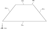
- FIG. 2 is a plan view showing an appearance of an example of the first protective member as viewed from the front side.
- Fig.3 (a) is a plane transparent view which shows the structure seen from the front side of an example of a 1st solar cell part.
- FIG. 3 (b) is a view showing an example of a virtual cut surface portion of the first solar cell unit taken along line IIIb-IIIb of FIG. 3 (a).
- FIG. 4 is a transparent plan view showing a structure of an example of the second solar cell unit as viewed from the front side.
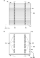
- Fig.5 (a) is a top view which shows the external appearance seen from the front side of an example of a 2nd solar cell element.
- FIG.5 (b) is a top view which shows the external appearance seen from the back surface side of an example of a 2nd solar cell element.
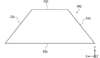
- FIG. 6 is a plan view showing an appearance of an example of the second protective member as viewed from the back side.
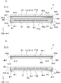
- FIGS. 7 (a) and 7 (b) are virtual cutting plane parts corresponding to the virtual cutting plane part of FIG. 1 (b) in the state in the middle of manufacturing the solar cell apparatus according to the first embodiment, respectively.
- FIG. 8 is a transparent plan view showing the structure of the first solar cell unit of the example of the solar cell device according to the second embodiment as viewed from the front side.
- FIG. 9 is a transparent plan view showing an appearance of a second solar cell portion and a reflection portion in an example of the solar cell device according to the third embodiment, viewed from the front side.
- FIGS. 10 (a) and 10 (b) respectively correspond to virtual cut surfaces along line Ib-Ib in FIG. 1 (a) in an example of the solar cell apparatus according to the fourth embodiment. It is a figure which shows a cut surface part.
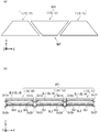
- Fig.11 (a) is a top view which shows the external appearance seen from the front side of an example of the solar cell array which concerns on 5th Embodiment.
- FIG. 11B is a cross-sectional view schematically showing a cross section of an example of the solar cell array according to the fifth embodiment.
- the direction along the eaves of the roof surface as the installation target surface Sp0 in the solar cell device 1 of FIG. 1A is taken as the + X direction.
- the direction orthogonal to the + X direction along the roof surface as the installation target surface Sp0 is the + Y direction.
- the normal direction of the installation target surface Sp0 is the + Z direction.
- an upper surface (also referred to as a roof surface) of a roof is adopted as a surface (also referred to as an installation target surface) Sp0 on which the solar cell device 1 is to be installed.
- a solar cell module having a trapezoidal shape in a plan view will be described by way of example so that the installation target surface Sp ⁇ b> 0 conforms to a trapezoidal roof surface of a dormitory structure.
- the solar cell apparatus 1 mainly includes a light receiving surface (also referred to as a front surface) 1 fs on which light is incident, and a back surface 1 bs opposite to the front surface 1 fs. And.
- the front surface 1 fs is in the state of facing the + Z direction.
- the back surface 1bs is in the state of facing the -Z direction.
- the + Z direction is set to the direction toward the sun that is traveling south.
- the front surface 1 fs and the back surface 1 bs have a trapezoidal shape.
- the solar cell module includes, for example, a solar cell panel PN1 and terminal boxes Bx1 and Bx2.
- the solar cell panel PN1 includes, for example, a first protective member PR1, a first solar cell unit SL1, a second solar cell unit SL2, and a second protective member PR2.
- the solar cell panel PN1 includes, for example, the sealing material F1 and the packing portion Pk0.
- the first protection member PR1 and the second protection member PR2 are positioned to face each other.
- the sealing material F1, the first solar cell unit SL1, the second solar cell unit SL2, and the packing unit Pk0 are located between the first protective member PR1 and the second protective member PR2.
- the sealing material F1 includes a first sealing material F1u and a second sealing material F1b.
- the first protective member PR1, the first solar cell unit SL1, the first sealing material F1u, the second solar cell unit SL2, and the The second sealing member F1b and the second protective member PR2 are positioned in the state of being stacked in this order.
- the packing portion Pk0 is located, for example, along the outer peripheral portion of the region between the first protection member PR1 and the second protection member PR2.
- the packing portion Pk0 has, for example, an outer peripheral portion of a region including the first solar cell unit SL1, the first sealing material F1u, the second solar cell unit SL2, and the second sealing material F1b. It is located to surround.
- the terminal boxes Bx1 and Bx2 are located, for example, on the back surface 1bs.
- the terminal boxes Bx1 and Bx2 are fixed on the back surface 1bs with an adhesive such as a silicone resin, for example.
- the terminal boxes Bx1 and Bx2 are, for example, in a state of being electrically connected to the wirings Wr1 and Wr2 connected to the first solar cell unit SL1 and the second solar cell unit SL2.
- the wiring Wr1 is, for example, in a state in which the first electrodes (positive electrode or negative electrode) of the first solar cell unit SL1 and the second solar cell unit SL2 are electrically connected to the terminals in the terminal box Bx1.
- the wiring Wr1 is drawn from the region between the first protection member PR1 and the second protection member PR2 to the back surface 1bs side of the second protection member PR2 through the through hole H1 of the second protection member PR2.
- the wiring Wr2 electrically connects, for example, the second electrode (negative electrode or positive electrode) opposite to the first electrode of the first solar cell unit SL1 and the second solar cell unit SL2 and the terminal in the terminal box Bx2.
- the wiring Wr2 is drawn from the region between the first protection member PR1 and the second protection member PR2 to the back surface 1bs side of the second protection member PR2 via the through hole H2 of the second protection member PR2.
- the terminal boxes Bx1 and Bx2 can output, for example, the electricity obtained by the power generation in the first solar cell unit SL1 and the second solar cell unit SL2 to the outside through a cable or the like.
- the first protective member PR1 is a member having translucency.
- the first protective member PR1 is, for example, a member constituting the front surface 1 fs of the solar cell panel PN1.
- the first protective member PR1 has, for example, a light transmitting property to light of a specific range of wavelength.
- the wavelength of the specific range for example, the wavelength of light which can be photoelectrically converted by the first solar cell unit SL1 and the second solar cell unit SL2 is adopted. If the wavelength of the light with high irradiation intensity which comprises sunlight is contained in the wavelength of a specific range, the photoelectric conversion efficiency of the solar cell apparatus 1 may improve.
- first protective member PR1 If, for example, a resin such as glass or acrylic or polycarbonate is applied to the material of the first protective member PR1, water shielding and light transmitting property to light of a specific range of wavelength are realized.
- a flat plate having a thickness of about 1 mm to 5 mm is applied to the first protective member PR1.
- the first protective member PR1 having the above configuration can protect the first solar cell unit SL1 and the second solar cell unit SL2 from the front surface 1fs side, for example, by rigidity and water blocking.
- the first protective member PR ⁇ b> 1 has a trapezoidal outer shape in plan view.
- the first protective member PR1 has, for example, a first side E1a and a second side E1b located along the + X direction as the first direction in plan view and located on opposite sides to each other.
- the third side E1c and the third side E1c as the oblique side positioned in a state of being inclined with respect to both the first side E1a and the second side E1b It has four sides E1d.
- the first solar cell unit SL1 is located closer to the first protective member PR1 than the second solar cell unit SL2. As shown in FIGS. 3A and 3B, the first solar cell unit SL1 includes, for example, a plurality of solar cell elements (also referred to as first solar cell elements) C1. In the first solar cell unit SL1, for example, the plurality of first solar cell elements C1 are located in a state of being aligned in a plane. Each first solar cell element C1 includes, for example, a thin film semiconductor (also referred to as a thin film semiconductor).
- arranging in a plane means that the respective first solar cell elements C1 are located and the plurality of first solar cell elements C1 are arranged along a virtual or actual plane.
- the plurality of first solar cell elements C1 are located on the first protective member PR1 acting as a substrate, aligned along the surface of the first protective member PR1.
- the first solar cell unit SL1 includes N (N is a natural number of 2 or more) first solar cell elements C1.
- N is a natural number of 2 or more
- each first solar cell element C1 has an elongated shape having a longitudinal direction along the first direction (+ X direction).
- the width of the first solar cell element C1 in the second direction is about several mm to 1 cm
- the first solar cell portion SL1 has several tens to several hundreds of first solar cell elements C1. It can be positioned side by side. And, for example, it is conceivable that the first direction is the horizontal direction.
- the solar cell device 1 even if a shadow extending along the second direction caused by the telegraph pole and the vertically elongated object such as a tree is formed on the solar cell device 1, the light irradiated to a part of the first solar cell elements C1 Is less likely to occur than the other second solar cell element C1. Therefore, for example, by electrically connecting the plurality of first solar cell elements C1 in series, it is possible to realize a somewhat high output voltage in the first solar cell portion SL1, while the first solar cell portion It is difficult to cause a significant drop in the output current in SL1.
- the first solar cell device 1 when viewed in a plan view, the first solar cell device 1 extends along the first direction (+ X direction) more than the length in the direction (also referred to as the vertical direction) along the second direction (+ Y direction).
- the width in the other direction also referred to as the lateral direction
- the width in the other direction also referred to as the lateral direction
- the output voltage of each first solar cell element C1 of the first solar cell unit SL1 is higher than the output voltage of each second solar cell element C2 described later of the second solar cell unit SL2
- the number of first solar cell elements C1 electrically connected in series in the first solar cell unit SL1 can be easily reduced.
- the output voltage (also referred to as a first output voltage) obtained in the first solar cell unit SL1 can be easily brought close to the output power (also referred to as a second output voltage) obtained in the second solar cell unit SL2.
- the output power also referred to as a second output voltage obtained in the second solar cell unit SL2.
- an electrical loss is less likely to occur, and the photoelectric conversion efficiency in the solar cell device 1 can be reduced. It can be improved.
- the first solar cell unit SL1 when the first solar cell unit SL1 is seen through in plan, if the areas of the plurality of first solar cell elements C1 are set to be constant, photoelectric conversion is performed in each first solar cell element C1. The obtained current tends to be the same. As a result, for example, even if the plurality of first solar cell elements C1 are electrically connected in series in order to improve the output voltage from the first solar cell unit SL1, electrical loss is unlikely to occur.
- Each 1st solar cell element C1 has the 1st electrode layer 1a, the semiconductor layer 1b, and the 2nd electrode layer 1c, as FIG. 3 (b) shows, for example. Further, in the first solar cell unit SL1, for example, as shown in FIG. 3B, the connection portion 4 exists between the adjacent first solar cell elements C1.
- first electrode layer 1a and the second electrode layer 1c have high transparency to light of a wavelength in a specific range than the semiconductor layer 1b, incident light is not transmitted to each first solar cell element C1. It can permeate
- the light which has not been absorbed by the semiconductor layer 1b but has passed through the semiconductor layer 1b passes through the second electrode layer 1c and is directed from the first solar cell unit SL1 to the second solar cell unit SL2. It is emitted.
- the first electrode layer 1a is located, for example, on the surface on the ⁇ Z side of the first protective member PR1.
- the first electrode layer 1a can collect, for example, charges generated by photoelectric conversion in response to light irradiation in the semiconductor layer 1b. If, for example, a transparent conductive oxide (TCO: Transparent Conductive Oxide) having translucency to light of a specific range of wavelength is applied to the material of the first electrode layer 1a, light of a specific range of wavelength is used. The light may pass through the first protective member PR1 and the first electrode layer 1a and be incident on the semiconductor layer 1b.
- the TCO can include, for example, indium tin oxide (ITO), fluorine-doped tin oxide (FTO), zinc oxide (ZnO), and the like.
- the six first electrode layers 1a are positioned on the first protective member PR1 so as to be planarly arranged along the + Y direction.
- the first electrode layer 1a of the m-th first solar cell element C1m (m is a natural number of 1 to 5) and the first electrode layer 1a of the (m + 1) -th first solar cell element C1 (m + 1) are located side by side across a gap (also referred to as a first gap) G1.
- the first electrode layer 1a of the first first solar cell element C11 and the first electrode layer 1a of the second first solar cell element C12 are arranged with a gap (also referred to as a first gap) G1 interposed therebetween.
- Each first gap G1 has a longitudinal direction along the + X direction. Further, there is a first groove P1 having the bottom face of the first protective member PR1 and the two end faces of the two first electrode layers 1a sandwiching the first gap G1 as opposed to each other.
- the semiconductor layer 1b is located between the first electrode layer 1a and the second electrode layer 1c.
- the semiconductor layer 1b of the m-th first solar cell element C1m is the -Y direction of the first electrode layer 1a of the (m + 1) -th first solar cell element C1 (m + 1) in the + Y direction.
- the semiconductor layer 1b of the first first solar cell element C11 extends over the end portion on the -Y direction side of the first electrode layer 1a of the adjacent second first solar cell element C12 in the + Y direction. positioned.
- the semiconductor layer 1 b is made of a thin film semiconductor.
- the thin film semiconductor for example, a compound semiconductor such as a CIS semiconductor, a CIGS semiconductor, a cadmium telluride (CdTe) semiconductor, or a compound having a perovskite structure is applied.
- the CIS semiconductor is a compound semiconductor containing cadmium (Cd), indium (In) and selenium (Se).
- the CIGS semiconductor is a compound semiconductor containing cadmium (Cd), indium (In), gallium (Ga) and selenium (Se).
- the first solar cell element C1 can mainly absorb visible light and use it for photoelectric conversion.
- an amorphous semiconductor such as amorphous silicon or a semiconductor of an organic thin film may be applied.
- the second electrode layer 1c is located on the semiconductor layer 1b.
- the second electrode layer 1c can collect charges generated by photoelectric conversion in response to light irradiation in the semiconductor layer 1b.
- a material of the second electrode layer 1c for example, a material having translucency to light of a wavelength in a specific range is applied as in the material of the first electrode layer 1a.
- a transparent conductive oxide (TCO) having translucency to light of a specific range of wavelength may be employed as a material of the second electrode layer 1c.
- TCO includes, for example, ITO, FTO or ZnO.
- the six second electrode layers 1c are located in a state where they are arranged in a plane along the + Y direction.
- the second electrode layer 1 c of the m-th first solar cell element C 1 m and the second electrode layer 1 c of the (m + 1) -th first solar cell element C 1 (m + 1) are also referred to as gaps (second gaps) )
- gaps (second gaps) ) are positioned side by side across G2.
- the second electrode layer 1c of the first first solar cell element C11 and the second electrode layer 1c of the second first solar cell element C12 are arranged with the gap (second gap) G2 interposed therebetween.
- Each second gap G2 has a longitudinal direction along the + X direction.
- a third groove portion P3 having the first electrode layer 1a as a bottom surface is configured.
- the second electrode layer 1c protrudes in the + Y direction more than the first electrode layer 1a.
- the second gap G2 is located at a position shifted in the second direction (+ Y direction) from the first gap G1.
- connection portion 4 is in a state in which two adjacent first solar cell elements C1 of the plurality of first solar cell elements C1 are electrically connected in series.
- the m-th connection portion 4m is positioned to penetrate the semiconductor layer 1b.
- the m-th connection unit 4m is in a state of electrically connecting the m-th first solar cell element C1m and the (m + 1) -th first solar cell element C1 (m + 1).
- the first connection portion 41 is in a state in which the first first solar cell element C11 and the second first solar cell element C12 are electrically connected.
- the m-th connection portion 4m includes the second electrode layer 1c of the m-th first solar cell element C1m and the (m + 1) -th first solar cell element C1 (m + 1) first electrode layer 1a. And are electrically connected.
- the first connection portion 41 electrically connects the second electrode layer 1c of the first first solar cell element C11 and the first electrode layer 1a of the second first solar cell element C12. In the state. Thereby, the plurality of first solar cell elements C1 can be electrically connected in series.
- the connection portion 4 is present in the second groove P2 with the end face of the semiconductor layer 1b as both side faces and the surface of the first electrode layer 1a in the -Z direction as the bottom face. Each second groove P2 has a longitudinal direction along the + X direction. Then, the connection portion 4 is filled in the second groove portion P2.
- first first solar cell element C11 a portion where the first electrode layer 1a protrudes in the -Y direction more than the semiconductor layer 1b and the second electrode layer 1c (also the first protrusion) Say) 1ae.
- the semiconductor layer 1b and the second electrode layer 1c are positioned so as to protrude in the + Y direction more than the first electrode layer 1a.
- a portion where the second electrode layer 1c protrudes in the + Y direction more than the first electrode layer 1a and the semiconductor layer 1b (a second protruding portion also have 1ce.
- An interconnection W1 for output of the first polarity (also referred to as a first interconnection W1a) is electrically connected on the first protrusion 1ae.
- the first wiring W1a is located along the end of the first first solar cell element C11 on the -Y direction side.
- a wire W1 for output of the second polarity (also referred to as a second wire W1b) is electrically connected on the second protrusion 1ce.
- the second wiring W1b is located along the edge on the + Y direction side of the sixth first solar cell element C16.
- the first polarity is a negative electrode
- the second polarity is a positive electrode.
- the second polarity is negative.
- the second solar cell unit SL2 is located between the first solar cell unit SL1 and the second protective member PR2. As shown in FIG. 4, the second solar cell unit SL2 includes, for example, a plurality of solar cell elements (also referred to as second solar cell elements) C2. In the second solar cell unit SL2, for example, the plurality of second solar cell elements C2 are positioned in a planar arrangement. Each second solar cell element C2 has a semiconductor substrate Su2 as shown in, for example, FIGS. 5 (a) and 5 (b). Further, for example, the plurality of second solar cell elements C2 are in a state of being electrically connected in series by the wiring W2.
- a semiconductor substrate Su2 as shown in, for example, FIGS. 5 (a) and 5 (b).
- the arrangement in a plane means that the respective second solar cell elements C2 are located along the virtual or actual plane and the plurality of second solar cell elements C2 are arranged.
- the plurality of second solar cell elements C2 are located in a line along the surface of the first protection member PR1.
- the second solar cell unit SL2 includes, for example, n (n is a natural number of 2 or more) second solar cell elements C2. In this case, for example, if n second solar cell elements C2 are electrically connected in series, the larger the numerical value n, the larger the output voltage of the second solar cell unit SL2.
- Each second solar cell element C2 can convert incident light energy into electrical energy. As shown in FIGS. 5A and 5B, the second solar cell element C2 is located on the surface (also referred to as a first element surface) Sf1 and on the back side of the first element surface Sf1. And a surface (also referred to as a second element surface) Sf2.
- the first element surface Sf1 of the second solar cell element C2 is mainly used as a light receiving surface to which light is incident
- the second element surface Sf2 of the second solar cell element C2 is mainly not incident to which light is not incident Used as a face.
- each second solar cell element C2 is, for example, the semiconductor substrate Su2, the surface side bus bar electrode EL1, the finger electrode EL2, and the extraction electrode (rear surface side bus bar electrode (Also referred to as “EL3”) and a collector electrode EL4.
- the semiconductor substrate Su2 mainly includes a region having one conductivity type and a reverse conductivity type layer.
- the opposite conductivity type layer is located, for example, on the first element surface Sf1 side on the + Z side of the semiconductor substrate Su2, and has a conductivity type opposite to one conductivity type of the semiconductor substrate Su2.
- an insulating layer as a reflection preventing layer is located in a region where the surface side bus bar electrode EL1 and the finger electrode EL2 are not formed on the opposite conductivity type layer.
- the surface side bus bar electrode EL1 and the finger electrode EL2 are located, for example, on the surface of the semiconductor substrate Su2 on the side of the first element surface Sf1.
- two substantially parallel surface-side bus bar electrodes EL1 are located on the first element surface Sf1 side, and a large number of substantially parallel finger electrodes EL2 are two surface side It is positioned to be substantially orthogonal to the bus bar electrode EL1.
- the back surface side bus bar electrode EL3 and the current collection electrode EL4 are located, for example, on the surface on the second element surface Sf2 side of the semiconductor substrate Su2.
- two rows of back surface side bus bar electrodes EL3 are located along the two substantially parallel imaginary lines on the second element surface Sf2 side.
- the back surface side bus bar electrode EL3 is formed except for the portion where the current collection electrode EL4 is connected by overlapping the back surface side bus bar electrode EL3 and the current collection electrode EL4. It is located on almost the entire surface of the unfilled area.
- Each of the two rows of back surface side bus bar electrodes EL3 is formed of, for example, four electrodes positioned in a line.
- the wiring W2 is, for example, the front side bus bar electrode EL1 of the first second solar cell element C2 and the back side bus bar electrode of the second second solar cell element C2 adjacent to the first second solar cell element C2. It is located in a state where it is electrically connected to EL3. Thereby, for example, the plurality of second solar cell elements C2 included in the second solar cell unit SL2 can be electrically connected in series. In the examples of FIG. 5A and FIG. 5B, the outer edge of the wiring W2 attached to each second solar cell element C2 is virtually drawn by a two-dot chain line.
- the wiring W2 is, for example, a linear or strip conductive metal.
- the wiring W2 for example, one in which a solder is coated on the entire surface of a copper foil having a thickness of about 0.1 mm to 0.5 mm and a width of about 1 mm to 10 mm may be employed.
- the wiring W2 is electrically connected to the front side bus bar electrode EL1 and the back side bus bar electrode EL3 by, for example, soldering.
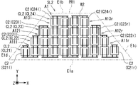
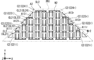
- a plurality of (here, 28) second solar cell elements C2 are arranged along both the + X direction as the first direction and the + Y direction as the second direction. Located in the state.
- 1st protection member PR1 it is located in the state in which the 2nd solar cell element C2 as many as possible is arranged.
- the plurality of second solar cell elements C2 configuring the second solar cell unit SL2 include two or more element rows CL2.
- Each element row CL2 includes, for example, two or more second solar cell elements C2 positioned in a state of being aligned along the + X direction as the first direction.
- the two or more element rows CL2 are positioned, for example, in a state of being aligned in the + Y direction as a second direction intersecting the first direction.
- the two or more element rows CL2 include a first element row CL21, a second element row CL22, a third element row CL23, and a fourth element row CL24.
- the first element row CL21 includes ten second solar cell elements C2 positioned in a line along the + X direction.
- the second element column CL22 includes eight second solar cell elements C2 positioned in a line along the + X direction.
- the third element column CL23 includes six second solar cell elements C2 positioned in a state of being aligned along the + X direction.
- the fourth element column CL24 includes four second solar cell elements C2 positioned in a state of being aligned along the + X direction.
- the end of the first element row CL21 on the + X direction side as the first direction and the end of the second element row CL22 on the side of the + X direction as the first direction deviate from each other In this state, the first element row CL21 and the second element row CL22 are located.
- the end of the second element row CL22 is shifted from the first element row CL21 in the ⁇ X direction as the third direction opposite to the first direction (+ X direction).
- the second solar cell element C2 located at the end on the first direction (+ X direction) side of the first element row CL21 is an end element (also referred to as a first end element) C21r.
- the second solar cell element C2 located at the end on the first direction (+ X direction) side of the second element column CL22 is an end element (also referred to as a second end element) C22r.
- the first end element C21r is located in a state of being deviated in the first direction (+ X direction) from the second end element C22r.
- the first end element C21r and the second end element C22r are the third side E1c of the first protective member PR1.
- the first element row CL21 and the second element row CL22 are positioned in line with each other.
- the end on the side of the third direction ( ⁇ X direction) opposite to the first direction of the first element row CL 21 and the third direction ( ⁇ X direction) of the second element row CL 22 The first element row CL21 and the second element row CL22 are positioned in a state in which they are offset from the end on the side of the first element line CL21.
- the second solar cell element C2 positioned at the end of the first element row CL21 on the side of the third direction (-X direction) is an end element C211
- the third direction of the second element row CL22 The second solar cell element C2 located at the end on the ( ⁇ X direction) side is an end element C221.
- the end element C211 is positioned in a state of being shifted in the third direction (-X direction) relative to the end element C221. Also, for example, when the second solar cell unit SL2 is seen through the front surface 1 fs in plan view, the end element C211 and the end element C221 are arranged along the fourth side E1d of the first protective member PR1. The first element row CL21 and the second element row CL22 are located.
- the end of the second element row CL22 in the first direction (+ X direction) is offset from the end of the third element row CL23 in the first direction (+ X direction).
- the second element row CL22 and the third element row CL23 are located.
- the second solar cell element C2 positioned at the end on the first direction (+ X direction) side of the third element column CL23 is taken as an end element C23r.
- the end element C22r is positioned to be deviated in the first direction (+ X direction) from the end element C23r.
- the end element C22r and the end element C23r are arranged along the third side E1c of the first protection member PR1.
- the second element row CL22 and the third element row CL23 are located.
- the end of the second element row CL22 in the third direction ( ⁇ X direction) and the end of the third element row CL23 in the third direction ( ⁇ X direction) are In the shifted state, the second element row CL22 and the third element row CL23 are located.
- the second solar cell element C2 positioned at the end of the third element row CL23 on the side in the third direction ( ⁇ X direction) is taken as an end element C231.
- the end element C221 is located in a state of being shifted in the third direction (-X direction) from the end element C231.
- the end element C221 and the end element C231 are arranged along the fourth side E1 d of the first protective member PR1.
- the second element row CL22 and the third element row CL23 are located.
- the end of the third element row CL23 in the first direction (+ X direction) is offset from the end of the fourth element row CL24 in the first direction (+ X direction).
- the third element row CL23 and the fourth element row CL24 are located.
- the second solar cell element C2 located at the end on the first direction (+ X direction) side of the fourth element column CL24 is taken as an end element C24r.
- the end element C23r is positioned to be deviated in the first direction (+ X direction) from the end element C24r.
- the end element C23r and the end element C24r are arranged along the third side E1c of the first protective member PR1.
- the third element row CL23 and the fourth element row CL24 are located.
- the end of the third element row CL23 in the third direction ( ⁇ X direction) and the end of the fourth element row CL24 in the third direction ( ⁇ X direction) are In the state of being shifted, the third element row CL23 and the fourth element row CL24 are located.
- the second solar cell element C2 positioned at the end of the fourth element row CL24 on the side in the third direction ( ⁇ X direction) is taken as an end element C24l.
- the end element C 23 l is positioned in a state of being deviated in the third direction ( ⁇ X direction) from the end element C 24 l.
- the end element C23l and the end element C24l are aligned along the fourth side E1d of the first protective member PR1.
- the third element row CL23 and the fourth element row CL24 are located.
- the area A1 includes, for example, areas A11 r, A11 l, A12 r, A12 l, A13 r, and A13 l.
- the area A11r is located on the first direction (+ X direction) side of the second element row CL22 when the first solar cell unit SL1 and the second solar cell unit SL2 are seen through in plan from the front side 1 fs side. This is a first region located between the element row CL21 and the second element row CL22.
- the area A11l is positioned on the side of the third direction (-X direction) with respect to the second element row CL22 when the first solar cell unit SL1 and the second solar cell unit SL2 are seen through in plan from the front side 1fs side.
- the region A12r is located on the first direction (+ X direction) side of the third element row CL23 when the first solar cell unit SL1 and the second solar cell unit SL2 are seen through the plane from the front side 1fs side. This is a region located between the element row CL22 and the third element row CL23.
- the area A12l is located on the side of the third element row CL23 in the third direction (-X direction) when the first solar cell unit SL1 and the second solar cell unit SL2 are seen through in plan from the front side 1fs side. This is a region located between the two-element row CL22 and the third-element row CL23.
- the region A13r is located on the first direction (+ X direction) side of the fourth element row CL24 when the first solar cell unit SL1 and the second solar cell unit SL2 are seen through the front surface 1 fs in plan view. This is a region located between the element row CL23 and the fourth element row CL24.
- the region A13l is located on the side of the fourth element row CL24 in the third direction (-X direction) when the first solar cell unit SL1 and the second solar cell unit SL2 are seen through in plan from the front side 1fs side. This is a region located between the three-element row CL23 and the fourth-element row CL24.
- the first solar cell unit SL1 and the second solar cell unit SL2 are seen through the plane from the front side 1 fs, a state in which a part of the plurality of first solar cell elements C1 is superimposed on the area A1.
- the area A1 as a blank portion where the second solar cell element C2 is not located is covered by the first solar cell element C1 of the first solar cell unit SL1. It is in the state of being
- each area A11 r, A11 l, A12 r, A12 l, A13 r, A13 l as a blank portion where the second solar cell element C2 is not located in the second solar cell unit SL2 is the first solar cell It is in a state of being covered by the element C1.
- the second solar cell unit SL2 for example, the light irradiated to the second solar cell unit SL2 without being absorbed by the first solar cell unit SL1 is used for power generation.
- the photoelectric conversion efficiency of the solar cell device 1 can be improved.
- the shapes of the plurality of second solar cell elements C2 and the like become difficult to see. In other words, for example, the presence of the region A1 as the blank portion of the second solar cell unit SL2 is difficult to see from the outside. For this reason, for example, the beauty of the solar cell device 1 can be improved. Therefore, for example, the photoelectric conversion efficiency and the appearance of the solar cell device 1 can be improved.
- the first solar cell element C1 overlaps in one or more areas A1.
- the photoelectric conversion efficiency of the solar cell device 1 can be improved.
- the first solar cell unit SL1 and the second solar cell unit SL2 are seen through from the front side 1 fs, if the entire area of one or more areas A1 is covered by the first solar cell element C1, The photoelectric conversion efficiency of the solar cell device 1 can be improved.
- the second protective member PR2 is, for example, a member that constitutes the back surface 1bs of the solar cell panel PN1. Therefore, for example, the second protective member PR2 can protect the first solar cell unit SL1 and the second solar cell unit SL2 from the back surface 1bs side.
- the second protective member PR2 is a plate having water shielding properties, the durability of the solar cell device 1 can be improved. If, for example, glass or a resin such as acrylic or polycarbonate is employed as the material of the second protective member PR2, the second protective member PR2 having water shielding is realized. At this time, for example, the second protective member PR2 has translucency to light of a wavelength in a specific range and high rigidity.
- the second protective member PR2 may not have translucency to light of a specific range of wavelengths, for example.
- the second protective member PR2 may be, for example, a back sheet made of resin.
- the second protective member PR2 may be, for example, a plate-like roofing material that constitutes a roof of a house or the like. In this case, the solar cell device 1 can be easily installed on the roof surface as the installation target surface Sp0.
- the second protective member PR2 has a trapezoidal outer shape when viewed in plan.
- the second protective member PR2 has, for example, a first side E1a and a second side E2b located along the + X direction as the first direction in plan view and located on opposite sides to each other.
- the second protection member PR2 has, for example, a third side E2c and a fourth side E2d positioned in a state of being inclined with respect to both the first side E1a and the second side E2b.
- the sealing material F1 is positioned in a state of being filled in a region covering at least the first solar cell unit SL1 and the second solar cell unit SL2 between the first protective member PR1 and the second protective member PR2 There is.
- the sealing material F1 includes, for example, a first sealing material F1 u on the front surface 1 fs side and a second sealing material F1 b on the back surface 1 bs side.
- the first sealing material F1u is located, for example, in a state of covering the entire surface of the first solar cell unit SL1 located on the first protective member PR1 on the second protective member PR2 side. Thereby, the first sealing material F1u can seal, for example, the first solar cell unit SL1. In addition, the first sealing material F1u is located, for example, in a state of covering the second solar cell unit SL2 from the side of the first protective member PR1. If it says from another viewpoint, the 1st sealing material F1 u is located in the state with which it is filled, for example between 1st solar cell part SL1 and 2nd solar cell part SL2.
- the second sealing material F1 b is located, for example, in a state of covering the second solar cell unit SL2 from the second protective member PR2 side. From another viewpoint, for example, the first sealing material F1u and the second sealing material F1b are positioned so as to surround the second solar cell unit SL2. Thereby, the first sealing material F1u and the second sealing material F1b can seal, for example, the second solar cell unit SL2.
- a material of the sealing material F1 for example, an ethylene-vinyl acetate copolymer (EVA) excellent in light transmittance to light of a specific range of wavelength, a polyester resin such as triacetyl cellulose (TAC) or polyethylene naphthalate It can be adopted.
- the sealing material F1 may be made of, for example, two or more types of materials.
- the packing portion Pk0 is located along the outer peripheral portion of the region between the first protective member PR1 and the second protective member PR2. From another point of view, the packing portion Pk0 is a portion of the region between the first protection member PR1 and the second protection member PR2 that is in the state of being annularly opened to the external space. It is located along (also referred to as an opening). The packing portion Pk0 is positioned, for example, to fill an area from the first protective member PR1 to the second protective member PR2. The packing portion Pk0 has higher water impermeability than the sealing material F1.
- the packing part Pk0 can seal the part along the outer peripheral part among the area
- the packing part Pk0 can reduce the penetration
- the long-term reliability of the solar cell device 1 can be enhanced.
- a butyl-based resin, a polyisopropylene-based resin, an acrylic resin, or the like is applied to the material of the packing portion Pk0.
- the first protective member PR1 is prepared.
- a flat glass plate or the like having trapezoidal front and back surfaces is prepared as the first protective member PR1.
- the first solar cell unit SL1 is disposed.
- the first solar cell unit SL1 is formed on one plate surface of the first protective member PR1.
- the first electrode layer 1a, the plurality of first groove portions P1 (first gap G1), the semiconductor layer 1b, the plurality of second groove portions P2, the first electrode layer 1a, the plurality of second groove portions P2, The two-electrode layer 2c, the connection portion 4 and the plurality of third grooves P3 (second gaps G2) are formed in this order of description.
- the first electrode layer 1a can be formed, for example, by film formation such as sputtering or vapor deposition on one surface of the first protective member PR1.
- the plurality of first groove portions P1 may be formed, for example, by separation of the first electrode layer 1a by laser irradiation or the like.
- the semiconductor layer 1b can be formed, for example, by applying a raw material liquid to the first electrode layer 1a and performing heat treatment.
- the plurality of second groove portions P2 may be formed, for example, by separation of the semiconductor layer 1b by scribing or the like.
- the second electrode layer 2c can be formed, for example, by sputtering or vapor deposition on the semiconductor layer 1b.
- the second solar cell unit SL2 formed on a thin transparent substrate may be disposed on one plate surface of the first protective member PR1.
- the wiring W1 is disposed with respect to the first solar cell unit SL1.
- the top of the first protrusion 1ae along the edge on the -Y direction side of the first first solar cell element C11 The first wiring W1a is disposed on the At this time, for example, the first wiring W1a is connected on the first protrusion 1ae by soldering or the like.
- the second protrusion 1ce is formed on the second protrusion 1ce along the edge on the + Y direction side of the sixth first solar cell element C16. 2 Arrange the wiring W1b. At this time, for example, the second wiring W1b is connected on the second protrusion 1ce by soldering or the like.
- the second solar cell unit SL2 is prepared.
- a plurality of second solar cell elements C2 are manufactured.
- the plurality of second solar cell elements C2 are electrically connected in series by the wiring W2.
- the wiring W2 (second wiring) for connecting to the terminal of the terminal box Bx1 to the second solar cell element C2 at the first end of the plurality of second solar cell elements C2 electrically connected in series One wire W2a) is electrically connected.
- the wiring W2 for connecting to the terminal of the terminal box Bx2 to the second solar cell element C2 at the second end of the plurality of second solar cell elements C2 electrically connected in series (Also referred to as a second wiring W2b) is electrically connected.
- the SL2, the annular sheet Spk0, the second sheet Sf1b, and the second protection member PR2 are laminated in this order of description.
- laminated body Sk1 is formed.
- the first wires W1a and W2a are inserted into the through holes H1 of the second protective member PR2 as the wires Wr1.
- the second wires W1 b and W2 b are inserted into the through holes H2 of the second protective member PR2 as the wires Wr1.
- the wiring Wr1 may be inserted into the through hole H1 in the state of one wiring in which the first wiring W1a and the first wiring W2a are connected, for example, or the first wiring W1a and the first wiring W2a And may be inserted into the through hole H1 in the state of two wires arranged in parallel.
- the first sheet Sf1 u is, for example, a sheet made of a resin (such as EVA) which is a component of the first sealing material F1 u.
- the annular sheet Spk0 is, for example, a sheet made of a resin (such as a butyl-based resin) which is a component of the packing portion Pk0.
- the second sheet Sf1 b is, for example, a sheet made of a resin (such as EVA) which is a base of the second sealing material F1 b.
- a resin such as EVA
- the annular sheet Spk0 is formed by directly applying the resin melted or semi-molten by heating on the annular portion along the outer edge portion of the first protection member PR1. Good.
- a lamination process is performed on the layered product Sk1 formed in the fifth step.
- a laminating apparatus (laminator) is used to integrate the laminated body Sk1.
- the laminate Sk1 is placed on a heater board in the chamber, and the laminate Sk1 is heated to about 100 ° C. to about 200 ° C. while the pressure in the chamber is reduced to about 50 Pa to about 150 Pa.
- the first sheet Sf1 u, the second sheet Sf1 b, and the third sheet Spk0 are in a state where they can flow to some extent by heating.
- the laminated body Sk1 is pressed by a diaphragm sheet or the like, and the laminated body Sk1 is integrated.
- the solar cell panel PN1 is formed.
- the terminal boxes Bx1 and Bx2 are attached to the solar cell panel PN1 formed in the sixth step.
- the terminal boxes Bx1 and Bx2 are attached on the back surface 1bs of the second protective member PR2.
- the terminal boxes Bx1 and Bx2 are arranged to cover the through holes H1 and H2.
- a resin such as a silicone sealant is used to back the second protective member PR2.
- the terminal boxes Bx1 and Bx2 are fixed on 1 bs. Thereby, the solar cell device 1 is formed.
- a frame is attached to the solar cell device 1 as needed.
- a frame made of aluminum is attached to the solar cell device 1 along the side surface of the solar cell device 1.
- a sealing material having excellent water shielding properties such as a butyl resin may be filled between the side surface of the solar cell device 1 and the frame.
- the solar cell device 1 for example, when the first solar cell unit SL1 and the second solar cell unit SL2 are seen through in plan view from the front side 1 fs, the second solar cell is used for the first protection member PR1.
- the region A1 is in a state of being covered by the first solar cell element C1 of the first solar cell unit SL1. Therefore, for example, the photoelectric conversion efficiency of the solar cell device 1 can be improved.
- the blank portion of the second solar cell unit SL2 is difficult to see from the outside. For this reason, for example, the beauty of the solar cell device 1 can be improved. Therefore, for example, the photoelectric conversion efficiency and the appearance of the solar cell device 1 can be improved. Further, for example, when a solar cell array is formed in which a plurality of solar cell devices 1 are arranged in a state where the plurality of solar cell devices 1 are arranged with respect to the installation target surface Sp0, photoelectric conversion efficiency and appearance in the solar cell array are improved. be able to.
- the first solar cell unit SL1 has a plurality of areas (also referred to as element areas) Ae1 each including two or more first solar cell elements C1. It may be changed to the first solar cell unit SL1A.
- each element region Ae1 includes two or more first solar cell elements C1 positioned in a state of being electrically connected in series. Further, each of the plurality of element regions Ae1 and the second solar cell unit SL2 are electrically connected in parallel.
- the plurality of element regions Ae1 include a first element region Ae11, a second element region Ae12, and a third element region Ae13.
- Each element region Ae1 includes six first solar cell elements C1.
- the first element region Ae11, the second element region Ae12, and the third element region Ae13 each have the same structure as that of the first solar cell unit SL1 shown in FIG. 3A.
- the first wiring W1a is electrically connected to the electrode of the first polarity
- the second wiring W1b is electrically connected to the electrode of the second polarity.
- the three first wirings W1a are electrically connected, and the three second wirings W1b are electrically connected, so that the plurality of element regions Ae1 are electrically connected in parallel to one another.
- an output voltage according to photoelectric conversion in each element region Ae1 and an output voltage according to photoelectric conversion in the second solar cell unit SL2 are substantially the same.
- an electrical loss hardly occurs, and the photoelectric conversion efficiency of the solar cell device 1 can be improved. it can.
- the wiring W1 may be drawn out of the solar cell device 1.
- downsizing of the configuration of the through holes H1, H2 and the like for passing the wiring W1 in at least one of the first protection member PR1 and the second protection member PR2 can be achieved.
- the durability of the second protective member PR2 can be improved.
- the reliability of the solar cell device 1 can be improved.
- entry of moisture through the configuration of the through holes H1, H2 and the like for passing the wiring W1 can be reduced. Therefore, for example, the reliability of the solar cell device 1 can be improved.
- the reflective portion Mr2 may be located.
- the reflective part Mr2 is positioned to face, for example, the first solar cell part SL1 (SL1A), and can reflect light.
- the reflection part Mr2 is located between the first solar cell part SL1 (SL1A) and the second protection member PR2.
- the reflecting portion Mr2 may be located, for example, on the surface or inside of the second protective member PR2.
- the reflective unit Mr2 corresponds to the first solar cell unit SL1 in the area A1. It may be located between the second protection member PR2 and at least one region of the second protection member PR2.
- a metal plate having a mirror-like surface or a white resin flat plate or sheet may be applied to the reflecting portion Mr2.
- the reflection part Mr2 exists, for example, the light is reflected in the solar cell device 1 and the light is irradiated to the first solar cell part SL1 (SL1A), the second solar cell part SL2, etc. be able to. Therefore, for example, incident light is easily absorbed in the first solar cell unit SL1 (SL1A) and the second solar cell unit SL2. Thereby, for example, light can be effectively used for power generation. As a result, for example, the photoelectric conversion efficiency in the solar cell device 1 can be improved.
- the solar cell device 1 includes the first panel portion PN1a and the second panel portion PN1b. It may be changed to 1C.
- the first panel unit PN1a includes, for example, a first solar cell unit SL1 (SL1A).
- the second panel unit PN1b includes, for example, a second solar cell unit SL2.
- the solar cell device 1C includes, for example, the first light transmitting member PR3, the second light transmitting member PR4, the first sealing member F1aC, and the second sealing member F1bC. Good.
- the first light transmitting member PR3 and the second light transmitting member PR4 are located, for example, between the first solar cell unit SL1 and the second solar cell unit SL2.
- Each of the first light transmitting member PR3 and the second light transmitting member PR4 has, for example, a light transmitting property with respect to light of a specific range of wavelength.
- the first sealing material F1aC is located, for example, in a state of covering the first solar cell unit SL1 (SL1A) between the first protective member PR1 and the first light transmissive member PR3.
- the second sealing material F1bC is located, for example, in a state of covering the second solar cell unit SL2 between the second light transmitting member PR4 and the second protective member PR2.
- the solar cell device 1C includes a first panel portion PN1a having a first solar cell portion SL1 (SL1A), and a second panel portion PN1b having a second solar cell portion SL2. , Are located in a stacked state. Therefore, for example, in the cold season, the second panel portion PN1b having the second solar cell portion SL2 can be removed from the installation target surface Sp0, and infrared rays and the like can be directly taken into a structure such as a house. .
- a holder for separately and detachably holding the first panel portion PN1a and the second panel portion PN1b may be installed on the installation target surface Sp0.
- the first protective member PR1 and the first light transmissive member PR3 are positioned in a state of facing each other.
- the first solar cell unit SL1 is located between the first protective member PR1 and the first light transmissive member PR3.
- the first sealing material F1aC is located so as to cover the first solar cell unit SL1.
- An annular packing member Px0a is located along the outer periphery of the region between the first protective member PR1 and the first light transmissive member PR3.
- the terminal boxes Bx1C and Bx2C are located on the surface on the ⁇ Z direction side of the first light transmissive member PR3.
- the wire Wr1C in a state of being electrically connected to the electrode of the first polarity of the first solar cell unit SL1 (SL1A) passes through the through hole H1C of the first translucent member PR3 to form the terminal box Bx1C.
- the wire Wr2C in a state of being electrically connected to the electrode of the second polarity of the second solar cell unit SL2 is electrically connected to the terminal of the terminal box Bx2C through the through hole H2C of the first light transmissive member PR3. In the state of being connected.
- the first light transmissive member PR3 may have, for example, a sheet-like form having light transmissivity to light of a specific range of wavelength.
- the second light transmitting member PR4 and the second protection member PR2 are positioned in a state of facing each other.
- the second solar cell unit SL2 is located between the second light transmitting member PR4 and the second protective member PR2.
- the second sealing material F1bC is located so as to cover the second solar cell unit SL2.
- An annular packing member Px0b is located along the outer periphery of the region between the first protective member PR1 and the first light transmissive member PR3.
- a material of the second light transmitting member PR4 for example, a material similar to the first protective member PR1 is applied.
- a solar cell array AY1 may be employed in which the plurality of solar cell devices 1 and 1C are positioned on the installation target surface Sp0.
- the first solar cell unit SL1 and the second solar cell unit SL2 are electrically connected. It does not have to be done.
- the first solar cell units SL1 (SL1A) and the second solar cell units SL2 may be separately electrically connected in series over the plurality of solar cell devices 1 and 1C.
- the plurality of solar cell apparatuses 1 and 1C may be located in a state of being aligned in a plane with respect to one installation target surface Sp0.
- the first solar cell device 1f, the second solar cell device 1s, and the third solar cell device 1t as the plurality of solar cell devices 1 and 1C are arranged in a line. It is located in And, the first solar cell unit SL1 (SL1A) of the first solar cell device 1f, the first solar cell portion SL1 (SL1A) of the second solar cell device 1s, and the first solar cell portion of the third solar cell device 1t SL1 (SL1A) is in a state of being electrically connected in series.
- the second solar cell unit SL2 of the first solar cell device 1f, the second solar cell portion SL2 of the second solar cell device 1s, and the second solar cell portion SL2 of the third solar cell device 1t are electrically Connected in series with the
- the first solar cell unit 1 f is electrically connected to the first solar cell unit SL1 (SL1A) through the wiring Cb1 and exposed to the outside through the first terminal portion Cn1 a and the second terminal portion Cn1.
- the terminal portion Cn1 b is present.
- the third terminal Cn1c and the fourth terminal Cn1d are electrically connected to the first solar cell SL1 (SL1A) through the wiring Cb1 and exposed to the outside to the second solar cell device 1s.
- a third terminal Cn1e and a sixth terminal Cn1f are electrically connected to the first solar cell SL1 (SL1A) through the wiring Cb1 and exposed to the outside to the third solar cell device 1t. Exists.
- the first solar cell portion SL1 (SL1A) of the first solar cell device 1 f and the first solar cell of the second solar cell device 1 s The battery unit SL1 (SL1A) is electrically connected in series.
- the first solar cell portion SL1 (SL1A) of the second solar cell device 1s and the first solar cell portion of the third solar cell device 1t SL1 (SL1A) is in a state of being electrically connected in series.
- the first terminal portion Cn2a and the first terminal portion Cn2a which are electrically connected to the second solar cell portion SL2 through the wiring Cb1 and exposed to the outside are provided.
- the second terminal portion Cn2b is present.
- a third terminal portion Cn2c and a fourth terminal portion Cn2d which are electrically connected to the second solar cell portion SL2 via the wiring Cb1 and are exposed to the outside Exists.
- a fifth terminal Cn2e and a sixth terminal Cn2f which are electrically connected to the second solar cell SL2 via the wiring Cb1 and exposed to the outside. Exists.
- the second solar cell portion SL2 of the first solar cell device 1f and the second solar cell portion SL2 of the second solar cell device 1s And are electrically connected in series.
- the fourth terminal portion Cn2d and the fifth terminal portion Cn2e are connected, the second solar cell portion SL2 of the second solar cell device 1s and the second solar cell portion SL2 of the third solar cell device 1t, Are electrically connected in series.
- the same type first solar cell units SL1 (SL1A) are electrically connected in series, the output is taken out, and the same type second solar cell units SL2 are electrically connected in series If a structure for taking out the output is adopted, it is possible to obtain an output that is respectively adapted to different voltage applications.
- applications of different voltages for example, an application as a household power supply and an application as a power supply for charging an electric vehicle etc. can be considered.
- the difference between the output voltages of the first solar cell units SL1 (SL1A) of the same type can be compared with the output voltage between the first solar cell units SL1 (SL1A) and the second solar cell units SL2 of different types. Making it smaller than the difference can be realized relatively easily. Therefore, for example, between the first solar cell unit SL1 (SL1A) and the second solar cell unit SL2 by the series connection of the first solar cell units SL1 (SL1A) and the series connection of the second solar cell units SL2.
- the number of parts such as wiring and converter for matching the output voltage can be reduced.
- the plurality of first solar cell units SL1 (SL1A) are electrically connected in series, and the plurality of second solar cell units SL2 are electrically connected in series, and then the plurality of first solar cell units SL1 (SL1A)
- the solar cell unit SL1 (SL1A) and the plurality of second solar cell units SL2 may be electrically connected in parallel.
- a converter for matching the output voltage from the plurality of first solar cell units SL1 (SL1A) and the output voltage from the plurality of second solar cell units SL2 is appropriately provided around the inverter It may be positioned.
- the configuration of the solar cell array AY1 can be simplified, electrical loss is unlikely to occur. Therefore, for example, with regard to the solar cell array AY1 in which the plurality of solar cell devices 1 and 1C are arranged, the photoelectric conversion efficiency and the appearance can be improved.
- the front surface 1 fs and the back surface 1 bs may have a shape other than a trapezoidal shape such as a parallelogram.
- the first protection member PR1 when viewed in a plan view, one of the third side E1c and the fourth side E1d is perpendicular to both the first side E1a and the second side E1b, etc. It may not be inclined with respect to the first side E1a and the second side E1b.
- any one of the third side E2c and the fourth side E2d is perpendicular to both the first side E2a and the second side E2b. For example, it may not be inclined with respect to the first side E2a and the second side E2b.
- the amount of deviation between the end portions in the + X direction between the adjacent element rows CL2 corresponds to the pitch (arrangement interval) at which the second solar cell elements C2 are aligned in the element row CL2. It may be an amount, may be less than or greater than the pitch. From another point of view, for example, when the second solar cell unit SL2 is seen through in plan, the plurality of second solar cell elements C2 are positioned stepwise in the end in the + X direction of the adjacent element row CL2 Just do it.
- the shape of the second solar cell element C2 is not limited to a rectangular shape, and a triangular shape or a rectangular shape with chamfered corner portions
- other shapes may be used.
- the first direction may be a direction shifted from the horizontal direction.
- the through holes H1 and H2 may be located in at least one of the first protection member PR1 and the second protection member PR2.
- the wires Wr1, Wr1C, Wr2, Wr2C, etc. may be drawn out from the side surfaces of the solar cell devices 1 and 1C.
Landscapes
- Photovoltaic Devices (AREA)
Abstract
太陽電池装置は、透光性を有する第1部材、第2部材、第1太陽電池部および第2太陽電池部を備える。第1太陽電池部は、第1部材と第2部材との間に位置し、それぞれが薄膜半導体を有する複数の第1太陽電池素子を含む。第2太陽電池部は、第1太陽電池部と第2部材との間に位置し、それぞれが半導体基板を有する複数の第2太陽電池素子を含む。複数の第2太陽電池素子は、それぞれが第1方向に沿って並んだ状態で位置している複数の第2太陽電池素子を含み且つ第1方向と交差する第2方向に並んだ状態で位置している複数の素子列を含む。複数の素子列は、第1素子列と、端部が第1素子列よりも第1方向とは逆の第3方向にずれている状態で位置している第2素子列とを有する。平面透視した場合に、第2素子列よりも第1方向の側で第1素子列と第2素子列との間の第1領域に、複数の第1太陽電池素子の一部が重畳している状態で位置している。
Description
本開示は、太陽電池装置および太陽電池アレイに関する。
屋根などの設置対象面に複数の太陽電池モジュールが配置された太陽電池アレイが知られている(例えば、特許第3410315号の記載を参照)。ただし、例えば、寄棟造の屋根における設置対象面には、台形状あるいは三角形状の部分がある。このため、例えば、設置対象面の形状に合わせて三角形状の太陽電池モジュールなどを配置することで、設置対象面において太陽電池モジュールが配置されていない空白部を減少させ、光電変換効率および美観を向上させる技術が考えられている。
太陽電池装置および太陽電池アレイが開示される。
太陽電池装置の一態様は、透光性を有する第1保護部材と、第2保護部材と、第1太陽電池部と、第2太陽電池部と、を備えている。前記第1太陽電池部は、前記第1保護部材と前記第2保護部材との間に位置しており、それぞれが薄膜半導体を有する複数の第1太陽電池素子を含む。前記第2太陽電池部は、前記第1太陽電池部と前記第2保護部材との間に位置しており、それぞれが半導体基板を有する複数の第2太陽電池素子を含む。前記複数の第2太陽電池素子は、それぞれが第1方向に沿って並んだ状態で位置している複数の第2太陽電池素子を含んでおり、且つ前記第1方向と交差する第2方向に並んだ状態で位置している、複数の素子列を含む。前記複数の素子列は、第1素子列と、端部が前記第1素子列よりも前記第1方向とは逆の第3方向にずれている状態で位置している第2素子列と、を有する。前記第1太陽電池部および前記第2太陽電池部を平面透視した場合に、前記第2素子列よりも前記第1方向の側に位置し、且つ前記第1素子列と前記第2素子列との間に位置している第1領域に、前記複数の第1太陽電池素子の一部が重畳している状態で位置している。
太陽電池アレイの一態様は、複数の前記一態様に係る太陽電池装置、を備えている。該複数の太陽電池装置にわたって、前記第1太陽電池部同士と前記第2太陽電池部同士とが別々に電気的に直列に接続されている状態にある。
以下、各種実施形態を図面に基づいて説明する。図面においては同様な構成および機能を有する部分に同じ符号が付されており、下記説明では重複説明が省略される。図面は模式的に示されたものである。図1(a)から図11(b)には、右手系のXYZ座標系が付されている。このXYZ座標系では、図1(a)の太陽電池装置1のうちの設置対象面Sp0としての屋根面の軒に沿った方向が+X方向とされている。設置対象面Sp0としての屋根面に沿った、+X方向に直交する方向が+Y方向とされている。設置対象面Sp0の法線方向が+Z方向とされている。
<1.第1実施形態>
<1-1.太陽電池装置>
第1実施形態に係る太陽電池装置1の構成を、図1(a)から図6に基づいて説明する。ここでは、太陽電池装置1を設置する対象となる面(設置対象面ともいう)Sp0としては、例えば、屋根の上面(屋根面ともいう)が採用される。太陽電池装置1の一例として、設置対象面Sp0が寄棟造の台形状の屋根面に対して適合するように、平面視した場合の形状が台形状である太陽電池モジュールを挙げて説明する。
<1-1.太陽電池装置>
第1実施形態に係る太陽電池装置1の構成を、図1(a)から図6に基づいて説明する。ここでは、太陽電池装置1を設置する対象となる面(設置対象面ともいう)Sp0としては、例えば、屋根の上面(屋根面ともいう)が採用される。太陽電池装置1の一例として、設置対象面Sp0が寄棟造の台形状の屋根面に対して適合するように、平面視した場合の形状が台形状である太陽電池モジュールを挙げて説明する。
図1(a)および図1(b)で示されるように、太陽電池装置1は、主に光が入射する受光面(前面ともいう)1fsと、この前面1fsの逆側に位置する裏面1bsと、を有する。第1実施形態では、前面1fsが、+Z方向を向いている状態にある。裏面1bsが、-Z方向を向いている状態にある。例えば、+Z方向は、南中している太陽に向いた方向に設定される。図1(a)の例では、前面1fsおよび裏面1bsが、台形状の形状を有する。
図1(a)および図1(b)で示されるように、太陽電池モジュールは、例えば、太陽電池パネルPN1と、端子ボックスBx1,Bx2と、を備えている。
太陽電池パネルPN1は、例えば、第1保護部材PR1と、第1太陽電池部SL1と、第2太陽電池部SL2と、第2保護部材PR2と、を備えている。また、第1実施形態では、太陽電池パネルPN1は、例えば、封止材F1およびパッキング部Pk0を有する。ここでは、例えば、第1保護部材PR1と第2保護部材PR2とが対向するように位置している。第1保護部材PR1と第2保護部材PR2との間には、例えば、封止材F1と、第1太陽電池部SL1と、第2太陽電池部SL2と、パッキング部Pk0と、が位置している。封止材F1は、第1封止材F1uと、第2封止材F1bと、を含む。
図1(b)の例では、前面1fsから裏面1bsに向けて、第1保護部材PR1と、第1太陽電池部SL1と、第1封止材F1uと、第2太陽電池部SL2と、第2封止材F1bと、第2保護部材PR2とが、この記載の順に積層されている状態で位置している。パッキング部Pk0は、例えば、第1保護部材PR1と第2保護部材PR2との間の領域の外周部分に沿って位置している。換言すれば、パッキング部Pk0は、例えば、第1太陽電池部SL1と、第1封止材F1uと、第2太陽電池部SL2と、第2封止材F1bと、を含む領域の外周部分を囲むように位置している。
端子ボックスBx1,Bx2は、例えば、裏面1bs上に位置している。端子ボックスBx1,Bx2は、例えば、シリコーン系の樹脂などの接着剤で裏面1bs上に固定されている。端子ボックスBx1,Bx2は、例えば、第1太陽電池部SL1および第2太陽電池部SL2に接続された配線Wr1,Wr2に電気的に接続されている状態にある。配線Wr1は、例えば、第1太陽電池部SL1および第2太陽電池部SL2の第1電極(正極あるいは負極)と端子ボックスBx1内の端子とを電気的に接続している状態にある。この配線Wr1は、例えば、第1保護部材PR1と第2保護部材PR2との間の領域から、第2保護部材PR2の貫通孔H1を介して、第2保護部材PR2の裏面1bs側まで引き出されている状態で位置している。配線Wr2は、例えば、第1太陽電池部SL1および第2太陽電池部SL2の第1電極とは逆の第2電極(負極あるいは正極)と端子ボックスBx2内の端子とを電気的に接続している状態にある。この配線Wr2は、例えば、第1保護部材PR1と第2保護部材PR2との間の領域から、第2保護部材PR2の貫通孔H2を介して、第2保護部材PR2の裏面1bs側まで引き出されている状態で位置している。そして、端子ボックスBx1,Bx2は、例えば、第1太陽電池部SL1および第2太陽電池部SL2における発電で得られた電気をケーブルなどで外部に出力することができる。
<1-1-1.第1保護部材>
第1保護部材PR1は、透光性を有する部材である。第1保護部材PR1は、例えば、太陽電池パネルPN1の前面1fsを構成する部材である。この第1保護部材PR1は、例えば、特定範囲の波長の光に対する透光性を有する。特定範囲の波長としては、例えば、第1太陽電池部SL1および第2太陽電池部SL2が光電変換し得る光の波長が採用される。特定範囲の波長に、太陽光を構成する照射強度の高い光の波長が含まれれば、太陽電池装置1の光電変換効率が向上し得る。第1保護部材PR1の素材に、例えば、ガラスあるいはアクリルまたはポリカーボネートなどの樹脂が適用されれば、遮水性と特定範囲の波長の光に対する透光性とが実現される。第1保護部材PR1には、例えば、厚さが1mmから5mm程度の平板状のものが適用される。上記構成を有する第1保護部材PR1は、例えば、剛性と遮水性とによって、第1太陽電池部SL1および第2太陽電池部SL2を前面1fs側から保護することができる。
第1保護部材PR1は、透光性を有する部材である。第1保護部材PR1は、例えば、太陽電池パネルPN1の前面1fsを構成する部材である。この第1保護部材PR1は、例えば、特定範囲の波長の光に対する透光性を有する。特定範囲の波長としては、例えば、第1太陽電池部SL1および第2太陽電池部SL2が光電変換し得る光の波長が採用される。特定範囲の波長に、太陽光を構成する照射強度の高い光の波長が含まれれば、太陽電池装置1の光電変換効率が向上し得る。第1保護部材PR1の素材に、例えば、ガラスあるいはアクリルまたはポリカーボネートなどの樹脂が適用されれば、遮水性と特定範囲の波長の光に対する透光性とが実現される。第1保護部材PR1には、例えば、厚さが1mmから5mm程度の平板状のものが適用される。上記構成を有する第1保護部材PR1は、例えば、剛性と遮水性とによって、第1太陽電池部SL1および第2太陽電池部SL2を前面1fs側から保護することができる。
図1(a)および図2の例では、第1保護部材PR1は、平面視した場合に、台形状の外形を有する。ここで、第1保護部材PR1は、例えば、平面視した場合に、第1方向としての+X方向に沿って位置し、互いに逆側に位置している第1辺E1aおよび第2辺E1bを有する。また、第1保護部材PR1は、例えば、平面視した場合に、第1辺E1aおよび第2辺E1bの双方に対して傾斜している状態で位置している斜辺としての第3辺E1cおよび第4辺E1dを有する。
<1-1-2.第1太陽電池部>
第1太陽電池部SL1は、第2太陽電池部SL2よりも第1保護部材PR1側に位置している。図3(a)および図3(b)で示されるように、第1太陽電池部SL1は、例えば、複数の太陽電池素子(第1太陽電池素子ともいう)C1を有する。第1太陽電池部SL1では、例えば、複数の第1太陽電池素子C1が平面的に並んでいる状態で位置している。各第1太陽電池素子C1は、例えば、薄膜状の半導体(薄膜半導体ともいう)を有する。ここで、平面的に並ぶとは、仮想あるいは実際の平面に沿って、各第1太陽電池素子C1が位置しており且つ複数の第1太陽電池素子C1が並んでいることを意味する。第1実施形態では、複数の第1太陽電池素子C1は、基板として働く第1保護部材PR1上において第1保護部材PR1の表面に沿って並んでいる状態で位置している。ここで、例えば、第1太陽電池部SL1が、N個(Nは2以上の自然数)の第1太陽電池素子C1を含む場合を想定する。この場合、例えば、N個の第1太陽電池素子C1が電気的に直列に接続されれば、数値Nが大きければ大きい程、第1太陽電池部SL1の出力電圧が大きくなり得る。
第1太陽電池部SL1は、第2太陽電池部SL2よりも第1保護部材PR1側に位置している。図3(a)および図3(b)で示されるように、第1太陽電池部SL1は、例えば、複数の太陽電池素子(第1太陽電池素子ともいう)C1を有する。第1太陽電池部SL1では、例えば、複数の第1太陽電池素子C1が平面的に並んでいる状態で位置している。各第1太陽電池素子C1は、例えば、薄膜状の半導体(薄膜半導体ともいう)を有する。ここで、平面的に並ぶとは、仮想あるいは実際の平面に沿って、各第1太陽電池素子C1が位置しており且つ複数の第1太陽電池素子C1が並んでいることを意味する。第1実施形態では、複数の第1太陽電池素子C1は、基板として働く第1保護部材PR1上において第1保護部材PR1の表面に沿って並んでいる状態で位置している。ここで、例えば、第1太陽電池部SL1が、N個(Nは2以上の自然数)の第1太陽電池素子C1を含む場合を想定する。この場合、例えば、N個の第1太陽電池素子C1が電気的に直列に接続されれば、数値Nが大きければ大きい程、第1太陽電池部SL1の出力電圧が大きくなり得る。
図3(a)および図3(b)には、第2方向としての+Y方向に沿って複数個(ここでは6個)の第1太陽電池素子C1が並んでいる状態で位置している例が示されている。ここでは、例えば、各第1太陽電池素子C1が、第1方向(+X方向)に沿った長手方向を有する細長い形状を有する。この場合、例えば、第1太陽電池素子C1の第2方向における幅が数mmから1cm程度であれば、第1太陽電池部SL1には数十個から数百個の第1太陽電池素子C1が並んでいる状態で位置し得る。そして、例えば、第1方向が水平方向である場合が考えられる。この場合には、電信柱および樹木などの縦長の物体によって生じる第2方向に沿って延びる影が太陽電池装置1上に形成されても、一部の第1太陽電池素子C1に照射される光の量が他の第2太陽電池素子C1よりも著しく低下する不具合が生じにくい。このため、例えば、複数の第1太陽電池素子C1を電気的に直列に接続することで、第1太陽電池部SL1におけるある程度高い出力電圧を実現することが可能でありながら、第1太陽電池部SL1における出力電流の著しい低下が生じにくい。
ここで、例えば、平面視したときに、第1太陽電池装置1が、第2方向(+Y方向)に沿った方向(縦方向ともいう)の長さよりも、第1方向(+X方向)に沿った方向(横方向ともいう)の幅の方が長い形状(横長の形状ともいう)を有する場合を想定する。この場合には、例えば、第1太陽電池部SL1の各第1太陽電池素子C1の出力電圧が、第2太陽電池部SL2の後述する各第2太陽電池素子C2よりも出力電圧が高くても、第1太陽電池部SL1において電気的に直列接続される第1太陽電池素子C1の数を容易に少なくすることができる。これにより、例えば、第1太陽電池部SL1で得られる出力電圧(第1出力電圧ともいう)を、第2太陽電池部SL2で得られる出力電力(第2出力電圧ともいう)に容易に近づけることができる。その結果、例えば、第1太陽電池部SL1と第2太陽電池部SL2とを電気的に並列に接続する場合であっても、電気的なロスが生じにくく、太陽電池装置1における光電変換効率を向上させることができる。
また、ここで、例えば、第1太陽電池部SL1を平面透視した場合に、複数の第1太陽電池素子C1の面積が一定に設定されていれば、各第1太陽電池素子C1において光電変換で得られる電流が同一となりやすい。その結果、例えば、第1太陽電池部SL1からの出力電圧を向上させるために、複数の第1太陽電池素子C1を電気的に直列に接続しても、電気的なロスが生じにくい。
各第1太陽電池素子C1は、例えば、図3(b)で示されるように、第1電極層1aと、半導体層1bと、第2電極層1cと、を有する。また、第1太陽電池部SL1には、例えば、図3(b)で示されるように、隣り合う第1太陽電池素子C1の間に、接続部4が存在している。
ここでは、例えば、第1電極層1aおよび第2電極層1cが、半導体層1bよりも特定範囲の波長の光に対する透光性が高ければ、各第1太陽電池素子C1において、入射光が第1電極層1aおよび第2電極層1cを透過し得る。このような構成が採用されれば、例えば、第1保護部材PR1を透過した入射光が、第1電極層1aを透過して半導体層1bに照射され得る。このとき、例えば、入射光の一部が半導体層1bで吸収され得る。ここで、入射光のうちの半導体層1bで吸収されずに半導体層1bを通過した光は、第2電極層1cを透過し、第1太陽電池部SL1から第2太陽電池部SL2に向けて出射される。
第1電極層1aは、例えば、第1保護部材PR1の-Z側の面上に位置している。第1電極層1aは、例えば、半導体層1bにおける光の照射に応じた光電変換で生じた電荷を集めることができる。第1電極層1aの素材に、例えば、特定範囲の波長の光に対して透光性を有する透明導電性酸化物(TCO:Transparent Conductive Oxide)が適用されれば、特定範囲の波長の光が第1保護部材PR1と第1電極層1aとを透過して半導体層1bに入射され得る。TCOには、例えば、酸化インジウムスズ(ITO:Indium Tin Oxide)、フッ素ドープ酸化スズ(FTO:Fluorine-doped tin oxide)または酸化亜鉛(ZnO)などが含まれ得る。
図3(b)の例では、第1保護部材PR1の上において、6つの第1電極層1aが、+Y方向に沿って平面的に並んでいる状態で位置している。ここで、第mの第1太陽電池素子C1m(mは1から5の自然数)の第1電極層1aと、第(m+1)の第1太陽電池素子C1(m+1)の第1電極層1aとが、間隙(第1間隙ともいう)G1を挟んで並んでいる状態で位置している。例えば、第1の第1太陽電池素子C11の第1電極層1aと、第2の第1太陽電池素子C12の第1電極層1aとが、間隙(第1間隙ともいう)G1を挟んで並んでいる状態で位置している。各第1間隙G1は、+X方向に沿った長手方向を有する。また、第1保護部材PR1を底面とし、第1間隙G1を挟む2つの第1電極層1aの互いに対向する2つの端面を側面とする第1溝部P1が存在している。
半導体層1bは、第1電極層1aと第2電極層1cとの間に位置している。ここでは、第mの第1太陽電池素子C1mの半導体層1bは、+Y方向における隣の第(m+1)の第1太陽電池素子C1(m+1)のうちの第1電極層1aの-Y方向の側の端部上にかけて位置している。例えば、第1の第1太陽電池素子C11の半導体層1bは、+Y方向における隣の第2の第1太陽電池素子C12のうちの第1電極層1aの-Y方向の側の端部上にかけて位置している。半導体層1bは、薄膜半導体によって構成されている。ここで、薄膜半導体には、例えば、CIS半導体、CIGS半導体、カドミウムテルル(CdTe)半導体またはペロブスカイト構造を有する化合物などの化合物半導体が適用される。CIS半導体は、カドミウム(Cd)、インジウム(In)およびセレン(Se)を含む化合物半導体である。CIGS半導体は、カドミウム(Cd)、インジウム(In)、ガリウム(Ga)およびセレン(Se)を含む化合物半導体である。このとき、第1太陽電池素子C1は、主に可視光を吸収して光電変換に利用することができる。また、薄膜半導体には、例えば、アモルファスシリコンなどの非晶質の半導体または有機薄膜の半導体などが適用されてもよい。
第2電極層1cは、半導体層1bの上に位置している。第2電極層1cは、半導体層1bにおける光の照射に応じた光電変換で生じた電荷を集めることができる。第2電極層1cの素材には、例えば、第1電極層1aの素材と同様に、特定範囲の波長の光に対して透光性を有する素材が適用される。具体的には、第2電極層1cの素材として、例えば、特定範囲の波長の光に対して透光性を有する透明導電性酸化物(TCO)が採用され得る。TCOには、例えば、ITO、FTOまたはZnOなどが含まれる。
図3(b)の例では、6つの第2電極層1cが、+Y方向に沿って平面的に並んでいる状態で位置している。ここでは、第mの第1太陽電池素子C1mの第2電極層1cと、第(m+1)の第1太陽電池素子C1(m+1)の第2電極層1cとが、間隙(第2間隙ともいう)G2を挟んで並んでいる状態で位置している。例えば、第1の第1太陽電池素子C11の第2電極層1cと、第2の第1太陽電池素子C12の第2電極層1cとが、間隙(第2間隙)G2を挟んで並んでいる状態で位置している。各第2間隙G2は、+X方向に沿った長手方向を有する。また、第1電極層1aを底面とする第3溝部P3を構成している。各第1太陽電池素子C1において、第1電極層1aよりも第2電極層1cの方が+Y方向に飛び出している状態にある。別の観点から言えば、第2間隙G2は、第1間隙G1よりも第2方向(+Y方向)にずれた位置に存在している。
接続部4は、複数の第1太陽電池素子C1のうちの隣り合う2つの第1太陽電池素子C1を電気的に直列に接続している状態にある。図3(b)の例では、第mの接続部4mは、半導体層1bを貫通するように位置している。そして、第mの接続部4mは、第mの第1太陽電池素子C1mと第(m+1)の第1太陽電池素子C1(m+1)とを電気的に接続している状態にある。例えば、第1の接続部41が、第1の第1太陽電池素子C11と第2の第1太陽電池素子C12とを電気的に接続している状態にある。より具体的には、第mの接続部4mは、第mの第1太陽電池素子C1mの第2電極層1cと第(m+1)の第1太陽電池素子C1(m+1)の第1電極層1aとを電気的に接続している状態にある。例えば、第1の接続部41は、第1の第1太陽電池素子C11の第2電極層1cと第2の第1太陽電池素子C12の第1電極層1aとを電気的に接続している状態にある。これにより、複数の第1太陽電池素子C1が電気的に直列に接続され得る。また、接続部4は、半導体層1bの端面を両側面とし、第1電極層1aの-Z方向の面を底面とする第2溝部P2内に存在している。各第2溝部P2は、+X方向に沿った長手方向を有する。そして、この第2溝部P2に接続部4が充填されている状態にある。
第1の第1太陽電池素子C11では、第1電極層1aが、半導体層1bおよび第2電極層1cよりも、-Y方向に突出している状態で位置している部分(第1突出部ともいう)1aeを有する。第6の第1太陽電池素子C16では、半導体層1bおよび第2電極層1cは、第1電極層1aよりも+Y方向に突出している状態で位置している。そして、第6の第1太陽電池素子C16では、第2電極層1cが、第1電極層1aおよび半導体層1bよりも、+Y方向に突出している状態で位置している部分(第2突出部ともいう)1ceを有する。第1突出部1ae上には、第1の極性の出力用の配線W1(第1配線W1aともいう)が電気的に接続されている状態にある。このとき、例えば、第1の第1太陽電池素子C11の-Y方向の側の端辺に沿って、第1配線W1aが位置している。第2突出部1ce上には、第2の極性の出力用の配線W1(第2配線W1bともいう)が電気的に接続されている状態にある。このとき、例えば、第6の第1太陽電池素子C16の+Y方向の側の端辺に沿って、第2配線W1bが位置している。ここで、例えば、第1の極性が負極であれば、第2の極性が正極となる。例えば、第1の極性が正極であれば、第2の極性が負極となる。
<1-1-3.第2太陽電池部>
第2太陽電池部SL2は、第1太陽電池部SL1と第2保護部材PR2との間に位置している。図4で示されるように、第2太陽電池部SL2は、例えば、複数の太陽電池素子(第2太陽電池素子ともいう)C2を有する。第2太陽電池部SL2では、例えば、複数の第2太陽電池素子C2が平面的に配列された状態で位置している。各第2太陽電池素子C2は、例えば、図5(a)および図5(b)で示されるように、半導体基板Su2を有する。また、例えば、複数の第2太陽電池素子C2は、配線W2によって電気的に直列に接続されている状態にある。ここで、平面的に配列とは、仮想あるいは実際の平面に沿って、各第2太陽電池素子C2が位置しており且つ複数の第2太陽電池素子C2が配列していることを意味する。第1実施形態では、複数の第2太陽電池素子C2は、第1保護部材PR1の表面に沿って並んでいる状態で位置している。また、第2太陽電池部SL2が、例えば、n個(nは2以上の自然数)の第2太陽電池素子C2を含む場合を想定する。この場合、例えば、n個の第2太陽電池素子C2が電気的に直列に接続されれば、数値nが大きければ大きい程、第2太陽電池部SL2の出力電圧が大きくなり得る。
第2太陽電池部SL2は、第1太陽電池部SL1と第2保護部材PR2との間に位置している。図4で示されるように、第2太陽電池部SL2は、例えば、複数の太陽電池素子(第2太陽電池素子ともいう)C2を有する。第2太陽電池部SL2では、例えば、複数の第2太陽電池素子C2が平面的に配列された状態で位置している。各第2太陽電池素子C2は、例えば、図5(a)および図5(b)で示されるように、半導体基板Su2を有する。また、例えば、複数の第2太陽電池素子C2は、配線W2によって電気的に直列に接続されている状態にある。ここで、平面的に配列とは、仮想あるいは実際の平面に沿って、各第2太陽電池素子C2が位置しており且つ複数の第2太陽電池素子C2が配列していることを意味する。第1実施形態では、複数の第2太陽電池素子C2は、第1保護部材PR1の表面に沿って並んでいる状態で位置している。また、第2太陽電池部SL2が、例えば、n個(nは2以上の自然数)の第2太陽電池素子C2を含む場合を想定する。この場合、例えば、n個の第2太陽電池素子C2が電気的に直列に接続されれば、数値nが大きければ大きい程、第2太陽電池部SL2の出力電圧が大きくなり得る。
各第2太陽電池素子C2は、入射される光エネルギーを電気エネルギーに変換することができる。図5(a)および図5(b)で示されるように、第2太陽電池素子C2は、面(第1素子面ともいう)Sf1と、この第1素子面Sf1の裏側に位置している面(第2素子面ともいう)Sf2と、を有する。ここでは、例えば、第2太陽電池素子C2の第1素子面Sf1が主として光が入射される受光面として使用され、第2太陽電池素子C2の第2素子面Sf2が主として光が入射されない非受光面として使用される。
図5(a)および図5(b)の例では、各第2太陽電池素子C2は、例えば、半導体基板Su2と、表面側バスバー電極EL1と、フィンガー電極EL2と、取出電極(裏面側バスバー電極ともいう)EL3と、集電電極EL4と、を有する。
半導体基板Su2には、例えば、結晶シリコンなどの結晶系の半導体などが適用され得る。具体的には、半導体基板Su2は、主として一導電型を有する領域と、逆導電型層と、を備えている。逆導電型層は、例えば、半導体基板Su2の+Z側の第1素子面Sf1側に位置しており且つ該半導体基板Su2の一導電型とは逆の導電型を有する。例えば、逆導電型層上のうち、表面側バスバー電極EL1およびフィンガー電極EL2が形成されていない領域には、反射防止層としての絶縁層が位置している。
表面側バスバー電極EL1およびフィンガー電極EL2は、例えば、半導体基板Su2のうちの第1素子面Sf1側の面上に位置している。図5(a)の例では、第1素子面Sf1側に、略平行な2本の表面側バスバー電極EL1が位置しており、略平行な多数本のフィンガー電極EL2が、2本の表面側バスバー電極EL1に略直交するように位置している。
裏面側バスバー電極EL3および集電電極EL4は、例えば、半導体基板Su2のうちの第2素子面Sf2側の面上に位置している。図5(b)の例では、第2素子面Sf2側に、略平行な2本の仮想線に沿って2列の裏面側バスバー電極EL3が位置している。また、集電電極EL4が、第2素子面Sf2側において、裏面側バスバー電極EL3と集電電極EL4とが重畳することで接続されている状態にある部分を除き、裏面側バスバー電極EL3が形成されていない領域の略全面に位置している。2列の裏面側バスバー電極EL3のそれぞれは、例えば、一列に並んでいる状態で位置している4つの電極によって構成される。
配線W2は、例えば、第1の第2太陽電池素子C2の表面側バスバー電極EL1と、この第1の第2太陽電池素子C2に隣接する第2の第2太陽電池素子C2の裏面側バスバー電極EL3とを電気的に接続している状態で位置している。これにより、例えば、第2太陽電池部SL2に含まれる複数の第2太陽電池素子C2が電気的に直列に接続され得る。図5(a)および図5(b)の例では、各第2太陽電池素子C2に対して取り付けられる配線W2の外縁が仮想的に二点鎖線で描かれている。配線W2は、例えば、線状あるいは帯状の導電性金属である。この配線W2としては、例えば、厚さが0.1mmから0.5mm程度であり且つ幅が1mmから10mm程度である銅箔の全面にはんだが被覆されたものが採用され得る。配線W2は、例えば、はんだ付けによって、表面側バスバー電極EL1および裏面側バスバー電極EL3に電気的に接続される。
図4で示されるように、例えば、第1方向としての+X方向および第2方向としての+Y方向の双方に沿って複数個(ここでは28個)の第2太陽電池素子C2が配列している状態で位置している。ここでは、第1保護部材PR1の形状に合わせて、できるだけ多くの数の第2太陽電池素子C2が配列されている状態で位置している。
具体的には、例えば、第2太陽電池部SL2を構成する複数の第2太陽電池素子C2は、2つ以上の素子列CL2を含む。各素子列CL2は、例えば、第1方向としての+X方向に沿って並んでいる状態で位置している2つ以上の第2太陽電池素子C2を含む。また、2つ以上の素子列CL2は、例えば、第1方向に交差する第2方向としての+Y方向に並んでいる状態で位置している。図4の例では、2つ以上の素子列CL2は、第1素子列CL21、第2素子列CL22、第3素子列CL23および第4素子列CL24を含む。第1素子列CL21は、+X方向に沿って並んでいる状態で位置している10個の第2太陽電池素子C2を含む。第2素子列CL22は、+X方向に沿って並んでいる状態で位置している8個の第2太陽電池素子C2を含む。第3素子列CL23は、+X方向に沿って並んでいる状態で位置している6個の第2太陽電池素子C2を含む。第4素子列CL24は、+X方向に沿って並んでいる状態で位置している4個の第2太陽電池素子C2を含む。
別の観点から言えば、例えば、第1素子列CL21の第1方向としての+X方向の側における端部と、第2素子列CL22の第1方向としての+X方向の側における端部とがずれている状態で、第1素子列CL21と第2素子列CL22とが位置している。換言すれば、例えば、第2素子列CL22の端部が、第1素子列CL21よりも第1方向(+X方向)とは逆の第3方向としての-X方向にずれている状態にある。ここで、例えば、第1素子列CL21のうちの第1方向(+X方向)の側の端に位置する第2太陽電池素子C2を端部素子(第1端部素子ともいう)C21rとする。第2素子列CL22のうちの第1方向(+X方向)の側の端に位置する第2太陽電池素子C2を端部素子(第2端部素子ともいう)C22rとする。この場合、第1端部素子C21rが、第2端部素子C22rよりも第1方向(+X方向)にずれている状態で位置している。
また、図4の例では、前面1fs側から第2太陽電池部SL2を平面透視した場合に、第1端部素子C21rと第2端部素子C22rとが第1保護部材PR1の第3辺E1cに沿って並んでいる状態で、第1素子列CL21と第2素子列CL22とが位置している。このような複数の第2太陽電池素子C2の配置により、第1保護部材PR1の形状に合わせて、できるだけ多くの数の第2太陽電池素子C2が配列され得る。
また、図4の例では、第1素子列CL21の第1方向とは逆の第3方向(-X方向)の側における端部と、第2素子列CL22の第3方向(-X方向)の側における端部とがずれている状態で、第1素子列CL21と第2素子列CL22とが位置している。ここで、第1素子列CL21のうちの第3方向(-X方向)の側の端に位置する第2太陽電池素子C2を端部素子C21lとし、第2素子列CL22のうちの第3方向(-X方向)の側の端に位置する第2太陽電池素子C2を端部素子C22lとする。この場合、端部素子C21lが、端部素子C22lよりも第3方向(-X方向)にずれている状態で位置している。また、例えば、前面1fs側から第2太陽電池部SL2を平面透視した場合に、端部素子C21lと端部素子C22lとが第1保護部材PR1の第4辺E1dに沿って並んでいる状態で、第1素子列CL21と第2素子列CL22とが位置している。
また、図4の例では、第2素子列CL22の第1方向(+X方向)の側における端部と、第3素子列CL23の第1方向(+X方向)の側における端部とがずれている状態で、第2素子列CL22と第3素子列CL23とが位置している。ここで、例えば、第3素子列CL23のうちの第1方向(+X方向)の側の端に位置する第2太陽電池素子C2を端部素子C23rとする。この場合、端部素子C22rが、端部素子C23rよりも第1方向(+X方向)にずれている状態で位置している。また、例えば、前面1fs側から第2太陽電池部SL2を平面透視した場合に、端部素子C22rと端部素子C23rとが第1保護部材PR1の第3辺E1cに沿って並んでいる状態で、第2素子列CL22と第3素子列CL23とが位置している。
また、図4の例では、第2素子列CL22の第3方向(-X方向)の側における端部と、第3素子列CL23の第3方向(-X方向)の側における端部とがずれている状態で、第2素子列CL22と第3素子列CL23とが位置している。ここで、例えば、第3素子列CL23のうちの第3方向(-X方向)の側の端に位置する第2太陽電池素子C2を端部素子C23lとする。この場合、端部素子C22lが、端部素子C23lよりも第3方向(-X方向)にずれている状態で位置している。また、例えば、前面1fs側から第2太陽電池部SL2を平面透視した場合に、端部素子C22lと端部素子C23lとが第1保護部材PR1の第4辺E1dに沿って並んでいる状態で、第2素子列CL22と第3素子列CL23とが位置している。
また、図4の例では、第3素子列CL23の第1方向(+X方向)の側における端部と、第4素子列CL24の第1方向(+X方向)の側における端部とがずれている状態で、第3素子列CL23と第4素子列CL24とが位置している。ここで、例えば、第4素子列CL24のうちの第1方向(+X方向)の側の端に位置する第2太陽電池素子C2を端部素子C24rとする。この場合、端部素子C23rが、端部素子C24rよりも第1方向(+X方向)にずれている状態で位置している。また、例えば、前面1fs側から第2太陽電池部SL2を平面透視した場合に、端部素子C23rと端部素子C24rとが第1保護部材PR1の第3辺E1cに沿って並んでいる状態で、第3素子列CL23と第4素子列CL24とが位置している。
また、図4の例では、第3素子列CL23の第3方向(-X方向)の側における端部と、第4素子列CL24の第3方向(-X方向)の側における端部とがずれている状態で、第3素子列CL23と第4素子列CL24とが位置している。ここで、例えば、第4素子列CL24のうちの第3方向(-X方向)の側の端に位置する第2太陽電池素子C2を端部素子C24lとする。この場合、端部素子C23lが、端部素子C24lよりも第3方向(-X方向)にずれている状態で位置している。また、例えば、前面1fs側から第2太陽電池部SL2を平面透視した場合に、端部素子C23lと端部素子C24lとが第1保護部材PR1の第4辺E1dに沿って並んでいる状態で、第3素子列CL23と第4素子列CL24とが位置している。
ところで、例えば、第1太陽電池部SL1および第2太陽電池部SL2を前面1fs側から平面透視した場合に、第1保護部材PR1に対して、第2太陽電池素子C2が重畳していない領域A1がある。
図4の例では、領域A1は、例えば、領域A11r,A11l,A12r,A12l,A13r,A13lを含む。領域A11rは、第1太陽電池部SL1および第2太陽電池部SL2を前面1fs側から平面透視した場合に、第2素子列CL22よりも第1方向(+X方向)の側に位置し且つ第1素子列CL21と第2素子列CL22との間に位置している第1領域である。領域A11lは、第1太陽電池部SL1および第2太陽電池部SL2を前面1fs側から平面透視した場合に、第2素子列CL22よりも第3方向(-X方向)の側に位置し且つ第1素子列CL21と第2素子列CL22との間に位置している領域である。領域A12rは、第1太陽電池部SL1および第2太陽電池部SL2を前面1fs側から平面透視した場合に、第3素子列CL23よりも第1方向(+X方向)の側に位置し且つ第2素子列CL22と第3素子列CL23との間に位置している領域である。領域A12lは、第1太陽電池部SL1および第2太陽電池部SL2を前面1fs側から平面透視した場合に、第3素子列CL23よりも第3方向(-X方向)の側に位置し且つ第2素子列CL22と第3素子列CL23との間に位置している領域である。領域A13rは、第1太陽電池部SL1および第2太陽電池部SL2を前面1fs側から平面透視した場合に、第4素子列CL24よりも第1方向(+X方向)の側に位置し且つ第3素子列CL23と第4素子列CL24との間に位置している領域である。領域A13lは、第1太陽電池部SL1および第2太陽電池部SL2を前面1fs側から平面透視した場合に、第4素子列CL24よりも第3方向(-X方向)の側に位置し且つ第3素子列CL23と第4素子列CL24との間に位置している領域である。
ここで、例えば、第1太陽電池部SL1および第2太陽電池部SL2を前面1fs側から平面透視した場合に、領域A1に、複数の第1太陽電池素子C1の一部が重畳している状態で位置している。換言すれば、ここでは、例えば、第2太陽電池部SL2において第2太陽電池素子C2が位置していない空白部としての領域A1が、第1太陽電池部SL1の第1太陽電池素子C1によってカバーされている状態にある。
図4の例では、第1太陽電池部SL1および第2太陽電池部SL2を前面1fs側から平面透視した場合に、領域A11rに、複数の第1太陽電池素子C1の一部が重畳している状態で位置している。また、図4の例では、第1太陽電池部SL1および第2太陽電池部SL2を前面1fs側から平面透視した場合に、領域A11lに、複数の第1太陽電池素子C1の一部が重畳している状態で位置している。また、図4の例では、第1太陽電池部SL1および第2太陽電池部SL2を前面1fs側から平面透視した場合に、領域A12rに、複数の第1太陽電池素子C1の一部が重畳している状態で位置している。また、図4の例では、第1太陽電池部SL1および第2太陽電池部SL2を前面1fs側から平面透視した場合に、領域A12lに、複数の第1太陽電池素子C1の一部が重畳している状態で位置している。また、図4の例では、第1太陽電池部SL1および第2太陽電池部SL2を前面1fs側から平面透視した場合に、領域A13rに、複数の第1太陽電池素子C1の一部が重畳している状態で位置している。また、図4の例では、第1太陽電池部SL1および第2太陽電池部SL2を前面1fs側から平面透視した場合に、領域A13lに、複数の第1太陽電池素子C1の一部が重畳している状態で位置している。換言すれば、ここでは、例えば、第2太陽電池部SL2において第2太陽電池素子C2が位置していない空白部としての各領域A11r,A11l,A12r,A12l,A13r,A13lが、第1太陽電池素子C1でカバーされている状態にある。
このような構成が採用されれば、第2太陽電池部SL2では、例えば、第1太陽電池部SL1で吸収されずに第2太陽電池部SL2に照射された光が発電に利用される。これにより、例えば、太陽電池装置1の光電変換効率が向上し得る。さらに、例えば、第1太陽電池部SL1が第2太陽電池部SL2よりも前面1fs側に位置していれば、複数の第2太陽電池素子C2の形状などが見えにくくなる。換言すれば、例えば、第2太陽電池部SL2の空白部としての領域A1の存在が外部から見えにくくなる。このため、例えば、太陽電池装置1の美観を向上させることができる。したがって、例えば、太陽電池装置1の光電変換効率および美観を向上させることができる。
ここで、さらに、例えば、第1太陽電池部SL1および第2太陽電池部SL2を前面1fs側から平面透視した場合に、1つ以上の領域A1において、第1太陽電池素子C1が重畳している状態にある領域の面積が大きければ大きい程、太陽電池装置1の光電変換効率が向上し得る。さらに、例えば、第1太陽電池部SL1および第2太陽電池部SL2を前面1fs側から平面透視した場合に、1つ以上の領域A1の全域が第1太陽電池素子C1によってカバーされていれば、太陽電池装置1の光電変換効率が向上し得る。
<1-1-4.第2保護部材>
第2保護部材PR2は、例えば、太陽電池パネルPN1の裏面1bsを構成する部材である。このため、第2保護部材PR2は、例えば、第1太陽電池部SL1および第2太陽電池部SL2を裏面1bs側から保護することができる。ここで、例えば、第2保護部材PR2が、遮水性を有する板材であれば、太陽電池装置1の耐久性が向上し得る。第2保護部材PR2の素材として、例えば、ガラスあるいはアクリルまたはポリカーボネートなどの樹脂が採用されれば、遮水性を有する第2保護部材PR2が実現される。このとき、例えば、第2保護部材PR2は、特定範囲の波長の光に対する透光性と高い剛性とを有する。第2保護部材PR2としては、例えば、厚さが1mmから5mm程度の平板状のものが採用される。第2保護部材PR2は、例えば、特定範囲の波長の光に対する透光性を有していなくてもよい。第2保護部材PR2は、例えば、樹脂製のバックシートであってもよい。第2保護部材PR2は、例えば、家屋などの屋根を構成するプレート状の屋根材であってもよい。この場合には、設置対象面Sp0としての屋根面に太陽電池装置1を容易に設置することができる。
第2保護部材PR2は、例えば、太陽電池パネルPN1の裏面1bsを構成する部材である。このため、第2保護部材PR2は、例えば、第1太陽電池部SL1および第2太陽電池部SL2を裏面1bs側から保護することができる。ここで、例えば、第2保護部材PR2が、遮水性を有する板材であれば、太陽電池装置1の耐久性が向上し得る。第2保護部材PR2の素材として、例えば、ガラスあるいはアクリルまたはポリカーボネートなどの樹脂が採用されれば、遮水性を有する第2保護部材PR2が実現される。このとき、例えば、第2保護部材PR2は、特定範囲の波長の光に対する透光性と高い剛性とを有する。第2保護部材PR2としては、例えば、厚さが1mmから5mm程度の平板状のものが採用される。第2保護部材PR2は、例えば、特定範囲の波長の光に対する透光性を有していなくてもよい。第2保護部材PR2は、例えば、樹脂製のバックシートであってもよい。第2保護部材PR2は、例えば、家屋などの屋根を構成するプレート状の屋根材であってもよい。この場合には、設置対象面Sp0としての屋根面に太陽電池装置1を容易に設置することができる。
また、図6の例では、第2保護部材PR2は、例えば、平面視した場合に、台形状の外形を有する。ここで、第2保護部材PR2は、例えば、平面視した場合に、第1方向としての+X方向に沿って位置し、互いに逆側に位置している第1辺E1aおよび第2辺E2bを有する。また、この場合、第2保護部材PR2は、例えば、第1辺E1aおよび第2辺E2bの双方に対して傾斜している状態で位置している第3辺E2cおよび第4辺E2dを有する。
<1-1-5.封止材>
封止材F1は、第1保護部材PR1と第2保護部材PR2との間のうちの少なくとも第1太陽電池部SL1および第2太陽電池部SL2を覆う領域に充填されている状態で位置している。封止材F1は、例えば、前面1fs側の第1封止材F1uと裏面1bs側の第2封止材F1bとを含む。
封止材F1は、第1保護部材PR1と第2保護部材PR2との間のうちの少なくとも第1太陽電池部SL1および第2太陽電池部SL2を覆う領域に充填されている状態で位置している。封止材F1は、例えば、前面1fs側の第1封止材F1uと裏面1bs側の第2封止材F1bとを含む。
第1封止材F1uは、例えば、第1保護部材PR1上に位置している第1太陽電池部SL1の第2保護部材PR2側の全面を覆っている状態で位置している。これにより、第1封止材F1uは、例えば、第1太陽電池部SL1を封止することができる。また、第1封止材F1uは、例えば、第2太陽電池部SL2を第1保護部材PR1側から覆っている状態で位置している。別の観点から言えば、第1封止材F1uは、例えば、第1太陽電池部SL1と第2太陽電池部SL2との間に充填されている状態で位置している。第2封止材F1bは、例えば、第2太陽電池部SL2を第2保護部材PR2側から覆っている状態で位置している。別の観点から言えば、例えば、第1封止材F1uと第2封止材F1bとが第2太陽電池部SL2を囲むように位置している。これにより、第1封止材F1uと第2封止材F1bとが、例えば、第2太陽電池部SL2を封止することができる。封止材F1の素材としては、例えば、特定範囲の波長の光に対する透光性が優れたエチレン酢酸ビニル共重合体(EVA)、トリアセチルセルロース(TAC)あるいはポリエチレンナフタレートなどのポリエステル樹脂などが採用され得る。封止材F1は、例えば、2種類以上の素材によって構成されていてもよい。
<1-1-6.パッキング部>
パッキング部Pk0は、第1保護部材PR1と第2保護部材PR2との間の領域のうちの外周部に沿って位置している。別の観点から言えば、パッキング部Pk0は、第1保護部材PR1と第2保護部材PR2との間の領域のうち、外部空間に対して開口している環状に位置している状態にある部分(開口部分ともいう)に沿って位置している。パッキング部Pk0は、例えば、第1保護部材PR1から第2保護部材PR2に至る領域を埋めるように位置している。パッキング部Pk0は、封止材F1よりも高い遮水性を有する。このため、パッキング部Pk0は、例えば、第1保護部材PR1と第2保護部材PR2との間の領域のうちの外周部に沿った部分を封止することができる。これにより、パッキング部Pk0は、例えば、太陽電池装置1の外部から第1太陽電池部SL1および第2太陽電池部SL2に向けた水分などの侵入を低減することができる。その結果、例えば、太陽電池装置1における長期間の信頼性を高めることができる。パッキング部Pk0の素材には、例えば、ブチル系の樹脂、ポリイソプロピレン系の樹脂またはアクリル系の樹脂などが適用される。
パッキング部Pk0は、第1保護部材PR1と第2保護部材PR2との間の領域のうちの外周部に沿って位置している。別の観点から言えば、パッキング部Pk0は、第1保護部材PR1と第2保護部材PR2との間の領域のうち、外部空間に対して開口している環状に位置している状態にある部分(開口部分ともいう)に沿って位置している。パッキング部Pk0は、例えば、第1保護部材PR1から第2保護部材PR2に至る領域を埋めるように位置している。パッキング部Pk0は、封止材F1よりも高い遮水性を有する。このため、パッキング部Pk0は、例えば、第1保護部材PR1と第2保護部材PR2との間の領域のうちの外周部に沿った部分を封止することができる。これにより、パッキング部Pk0は、例えば、太陽電池装置1の外部から第1太陽電池部SL1および第2太陽電池部SL2に向けた水分などの侵入を低減することができる。その結果、例えば、太陽電池装置1における長期間の信頼性を高めることができる。パッキング部Pk0の素材には、例えば、ブチル系の樹脂、ポリイソプロピレン系の樹脂またはアクリル系の樹脂などが適用される。
<1-2.太陽電池装置の製造方法>
太陽電池装置1の製造方法の一例について、図7(a)および図7(b)に基づいて説明する。ここでは、例えば、第1工程から第8工程を順に実施することで、太陽電池装置1を製造することができる。
太陽電池装置1の製造方法の一例について、図7(a)および図7(b)に基づいて説明する。ここでは、例えば、第1工程から第8工程を順に実施することで、太陽電池装置1を製造することができる。
第1工程では、例えば、第1保護部材PR1を準備する。ここでは、例えば、第1保護部材PR1として、台形状の表裏面を有する平板状のガラス板などが準備される。
第2工程では、例えば、第1太陽電池部SL1を配置する。ここでは、例えば、第1保護部材PR1の一方の盤面上に第1太陽電池部SL1が形成される。具体的には、例えば、第1保護部材PR1の一方の盤面上に、第1電極層1a、複数の第1溝部P1(第1間隙G1)、半導体層1b、複数の第2溝部P2、第2電極層2cおよび接続部4ならびに複数の第3溝部P3(第2間隙G2)がこの記載順に形成される。第1電極層1aは、例えば、第1保護部材PR1の一方の盤面上に対するスパッタリングまたは蒸着などの成膜によって形成され得る。複数の第1溝部P1は、例えば、レーザーの照射などによる第1電極層1aの分離で形成され得る。半導体層1bは、例えば、第1電極層1a上に対する原料液の塗布および熱処理などで形成され得る。複数の第2溝部P2は、例えば、スクライビングなどによる半導体層1bの分離で形成され得る。第2電極層2cは、例えば、半導体層1b上に対するスパッタリングまたは蒸着などによって形成され得る。第2工程では、例えば、薄い透明基板上に形成された第2太陽電池部SL2が第1保護部材PR1の一方の盤面上に配置されてもよい。
第3工程では、例えば、第1太陽電池部SL1に対して配線W1を配置する。ここでは、例えば、図3(a)および図3(b)で示されたように、第1の第1太陽電池素子C11の-Y方向の側の端辺に沿った第1突出部1ae上に第1配線W1aを配置する。このとき、例えば、第1突出部1ae上に第1配線W1aがはんだ付けなどで接続される。また、例えば、図3(a)および図3(b)で示されたように、第6の第1太陽電池素子C16の+Y方向の側の端辺に沿った第2突出部1ce上に第2配線W1bを配置する。このとき、例えば、第2突出部1ce上に第2配線W1bがはんだ付けなどで接続される。
第4工程では、例えば、第2太陽電池部SL2を準備する。ここでは、例えば、まず、複数の第2太陽電池素子C2を作製する。次に、例えば、複数の第2太陽電池素子C2を平面的に配列しつつ、複数の第2太陽電池素子C2を配線W2によって電気的に直列に接続する。このとき、例えば、電気的に直列に接続された複数の第2太陽電池素子C2のうちの第1端の第2太陽電池素子C2に、端子ボックスBx1の端子に接続するための配線W2(第1配線W2aともいう)が電気的に接続される。また、このとき、例えば、電気的に直列に接続された複数の第2太陽電池素子C2のうちの第2端の第2太陽電池素子C2に、端子ボックスBx2の端子に接続するための配線W2(第2配線W2bともいう)が電気的に接続される。
第5工程では、例えば、図7(a)および図7(b)に示されるように、第1太陽電池部SL1が形成された第1保護部材PR1、第1シートSf1u、第2太陽電池部SL2、環状シートSpk0、第2シートSf1bおよび第2保護部材PR2をこの記載順に積層する。これにより、積層体Sk1が形成される。このとき、図7(b)で示されるように、例えば、第1配線W1a,W2aが、配線Wr1として、第2保護部材PR2の貫通孔H1に挿通される。また、例えば、第2配線W1b,W2bが、配線Wr1として、第2保護部材PR2の貫通孔H2に挿通される。ここで、配線Wr1は、例えば、第1配線W1aと第1配線W2aとが接続された1本の配線の状態で貫通孔H1に挿通されてもよいし、第1配線W1aと第1配線W2aとが並列して並べられた2本の配線の状態で貫通孔H1に挿通されてもよい。ここで、第1シートSf1uは、例えば、第1封止材F1uの素になる樹脂(EVAなど)製のシートである。環状シートSpk0は、例えば、パッキング部Pk0の素になる樹脂(ブチル系の樹脂など)製のシートである。第2シートSf1bは、例えば、第2封止材F1bの素になる樹脂(EVAなど)製のシートである。ここで、例えば、第1保護部材PR1の外縁部に沿った環状の部分の上に、加熱によって溶融または半溶融の状態とされた樹脂が直接塗布されることで環状シートSpk0が形成されてもよい。
第6工程では、例えば、第5工程で形成された積層体Sk1を対象としたラミネート処理を行う。ここでは、例えば、ラミネート装置(ラミネータ)が用いられて、積層体Sk1が一体化される。例えば、ラミネータでは、チャンバー内のヒーター盤上に積層体Sk1が載置され、チャンバー内が50Paから150Pa程度まで減圧されつつ、積層体Sk1が100℃から200℃程度まで加熱される。このとき、第1シートSf1u、第2シートSf1bおよび第3シートSpk0が加熱によってある程度流動可能な状態となる。この状態で、チャンバー内において、積層体Sk1が、ダイヤフラムシートなどで押圧され、積層体Sk1が一体化した状態となる。これにより、太陽電池パネルPN1が形成される。
第7工程では、例えば、第6工程で形成された太陽電池パネルPN1に端子ボックスBx1,Bx2を取り付ける。ここでは、例えば、図1(b)で示されるように、第2保護部材PR2の裏面1bs上に端子ボックスBx1,Bx2が取り付けられる。このとき、例えば、貫通孔H1,H2を覆うように、端子ボックスBx1,Bx2が配置される。そして、例えば、配線Wr1が端子ボックスBx1内の端子に接続され、配線Wr2が端子ボックスBx2内の端子に接続された状態で、シリコーンシーラントなどの樹脂が用いられて、第2保護部材PR2の裏面1bs上に端子ボックスBx1,Bx2が固定される。これにより、太陽電池装置1が形成される。
第8工程では、例えば、必要に応じて太陽電池装置1にフレームを取り付ける。ここでは、例えば、太陽電池装置1の側面に沿って、太陽電池装置1にアルミニウム製のフレームが取り付けられる。このとき、例えば、太陽電池装置1の側面と、フレームとの間にブチル系の樹脂などの遮水性の優れた封止材が充填されてもよい。
<1-3.第1実施形態のまとめ>
第1実施形態に係る太陽電池装置1では、例えば、第1太陽電池部SL1および第2太陽電池部SL2を前面1fs側から平面透視した場合に、第1保護部材PR1に対して、第2太陽電池素子C2が重畳していない空白部としての領域A1が存在している。ここで、例えば、領域A1が、第1太陽電池部SL1の第1太陽電池素子C1によってカバーされている状態にある。このため、例えば、太陽電池装置1の光電変換効率を向上させることができる。さらに、例えば、薄膜系の第1太陽電池部SL1を第2太陽電池部SL2よりも前面1fs側に配置することで、第2太陽電池部SL2の空白部が外部から見えにくくなる。このため、例えば、太陽電池装置1の美観を向上させることができる。したがって、例えば、太陽電池装置1の光電変換効率および美観を向上させることができる。また、例えば、仮に設置対象面Sp0に対して複数の太陽電池装置1が配列された状態で位置している太陽電池アレイが形成された場合において、太陽電池アレイにおける光電変換効率および美観を向上させることができる。
第1実施形態に係る太陽電池装置1では、例えば、第1太陽電池部SL1および第2太陽電池部SL2を前面1fs側から平面透視した場合に、第1保護部材PR1に対して、第2太陽電池素子C2が重畳していない空白部としての領域A1が存在している。ここで、例えば、領域A1が、第1太陽電池部SL1の第1太陽電池素子C1によってカバーされている状態にある。このため、例えば、太陽電池装置1の光電変換効率を向上させることができる。さらに、例えば、薄膜系の第1太陽電池部SL1を第2太陽電池部SL2よりも前面1fs側に配置することで、第2太陽電池部SL2の空白部が外部から見えにくくなる。このため、例えば、太陽電池装置1の美観を向上させることができる。したがって、例えば、太陽電池装置1の光電変換効率および美観を向上させることができる。また、例えば、仮に設置対象面Sp0に対して複数の太陽電池装置1が配列された状態で位置している太陽電池アレイが形成された場合において、太陽電池アレイにおける光電変換効率および美観を向上させることができる。
<2.他の実施形態>
本開示は上述の第1実施形態に限定されるものではなく、本開示の要旨を逸脱しない範囲において種々の変更、改良などが可能である。
本開示は上述の第1実施形態に限定されるものではなく、本開示の要旨を逸脱しない範囲において種々の変更、改良などが可能である。
<2-1.第2実施形態>
上記第1実施形態において、例えば、第1太陽電池部SL1が、図8で示されるように、2以上の第1太陽電池素子C1をそれぞれ含む、複数の領域(素子領域ともいう)Ae1を有する第1太陽電池部SL1Aに変更されてもよい。ここでは、例えば、各素子領域Ae1は、電気的に直列に接続されている状態で位置している、2つ以上の第1太陽電池素子C1を含む。また、複数の素子領域Ae1のそれぞれと、第2太陽電池部SL2とは電気的に並列に接続されている状態にある。
上記第1実施形態において、例えば、第1太陽電池部SL1が、図8で示されるように、2以上の第1太陽電池素子C1をそれぞれ含む、複数の領域(素子領域ともいう)Ae1を有する第1太陽電池部SL1Aに変更されてもよい。ここでは、例えば、各素子領域Ae1は、電気的に直列に接続されている状態で位置している、2つ以上の第1太陽電池素子C1を含む。また、複数の素子領域Ae1のそれぞれと、第2太陽電池部SL2とは電気的に並列に接続されている状態にある。
図8の例では、複数の素子領域Ae1は、第1素子領域Ae11、第2素子領域Ae12および第3素子領域Ae13を含む。各素子領域Ae1は、6つの第1太陽電池素子C1を含む。第1素子領域Ae11、第2素子領域Ae12および第3素子領域Ae13は、それぞれ図3(a)で示された第1太陽電池部SL1と同様な構造を有する。各素子領域Ae1においては、第1の極性の電極に第1配線W1aが電気的に接続され、第2の極性の電極に第2配線W1bが電気的に接続されている状態にある。そして、3本の第1配線W1aが電気的に接続され、3本の第2配線W1bが電気的に接続されていることで、複数の素子領域Ae1が相互に電気的に並列に接続されている状態にある。ここで、例えば、各素子領域Ae1における光電変換に応じた出力電圧と、第2太陽電池部SL2における光電変換に応じた出力電圧とが、ほぼ同一である場合を想定する。この場合には、各素子領域Ae1と、第2太陽電池部SL2と、を電気的に並列に接続すれば、電気的なロスが生じにくく、太陽電池装置1の光電変換効率を向上させることができる。
ここで、例えば、第1太陽電池部SL1Aと第2太陽電池部SL2とを配線W1によって電気的に並列に接続した後に、配線W1を太陽電池装置1の外に引き出してもよい。これにより、例えば、第1保護部材PR1および第2保護部材PR2の少なくとも一方における配線W1を通すための貫通孔H1,H2などの構成の小型化が図られ得る。これにより、例えば、第2保護部材PR2の耐久性が改善され得る。その結果、太陽電池装置1の信頼性の向上が図られ得る。また、例えば、配線W1を通すための貫通孔H1,H2などの構成を介した水分の侵入が低減され得る。したがって、例えば、太陽電池装置1の信頼性を向上させることができる。
<2-2.第3実施形態>
上記各実施形態において、例えば、図9で示されるように、第1太陽電池部SL1(SL1A)および第2太陽電池部SL2を前面1fs側から平面透視した場合に、空白部としての領域A1に、反射部Mr2が位置していてもよい。反射部Mr2は、例えば、第1太陽電池部SL1(SL1A)に対向するように位置し、光を反射することができる。図9の例では、反射部Mr2は、第1太陽電池部SL1(SL1A)と第2保護部材PR2との間に位置している。ここでは、反射部Mr2は、例えば、第2保護部材PR2の表面あるいは内部に位置していてもよい。換言すれば、例えば、第1太陽電池部SL1(SL1A)および第2太陽電池部SL2を前面1fs側から平面透視した場合に、反射部Mr2は、領域A1のうち、第1太陽電池部SL1と第2保護部材PR2との間および第2保護部材PR2の少なくとも1つの領域に位置していてもよい。反射部Mr2には、例えば、鏡面状の表面を有する金属板あるいは白い樹脂製の平板またはシートなどが適用され得る。
上記各実施形態において、例えば、図9で示されるように、第1太陽電池部SL1(SL1A)および第2太陽電池部SL2を前面1fs側から平面透視した場合に、空白部としての領域A1に、反射部Mr2が位置していてもよい。反射部Mr2は、例えば、第1太陽電池部SL1(SL1A)に対向するように位置し、光を反射することができる。図9の例では、反射部Mr2は、第1太陽電池部SL1(SL1A)と第2保護部材PR2との間に位置している。ここでは、反射部Mr2は、例えば、第2保護部材PR2の表面あるいは内部に位置していてもよい。換言すれば、例えば、第1太陽電池部SL1(SL1A)および第2太陽電池部SL2を前面1fs側から平面透視した場合に、反射部Mr2は、領域A1のうち、第1太陽電池部SL1と第2保護部材PR2との間および第2保護部材PR2の少なくとも1つの領域に位置していてもよい。反射部Mr2には、例えば、鏡面状の表面を有する金属板あるいは白い樹脂製の平板またはシートなどが適用され得る。
このように、反射部Mr2が存在していれば、例えば、太陽電池装置1内で光を反射させて、第1太陽電池部SL1(SL1A)および第2太陽電池部SL2などに光を照射することができる。このため、例えば、第1太陽電池部SL1(SL1A)および第2太陽電池部SL2において、入射光が吸収されやすくなる。これにより、例えば、光を発電に有効利用することができる。その結果、例えば、太陽電池装置1における光電変換効率の向上が図られ得る。
<2-3.第4実施形態>
上記各実施形態において、例えば、図10(a)および図10(b)で示されるように、太陽電池装置1が、第1パネル部PN1aと、第2パネル部PN1bと、を有する太陽電池装置1Cに変更されてもよい。第1パネル部PN1aは、例えば、第1太陽電池部SL1(SL1A)を含む。第2パネル部PN1bは、例えば、第2太陽電池部SL2を含む。ここでは、太陽電池装置1Cは、例えば、第1透光性部材PR3と、第2透光性部材PR4と、第1封止材F1aCと、第2封止材F1bCと、を備えていてもよい。第1透光性部材PR3および第2透光性部材PR4は、例えば、第1太陽電池部SL1と第2太陽電池部SL2との間に位置している。第1透光性部材PR3および第2透光性部材PR4は、例えば、それぞれ特定範囲の波長の光に対する透光性を有する。第1封止材F1aCは、例えば、第1保護部材PR1と第1透光性部材PR3との間において第1太陽電池部SL1(SL1A)を覆っている状態で位置している。第2封止材F1bCは、例えば、第2透光性部材PR4と第2保護部材PR2との間において第2太陽電池部SL2を覆っている状態で位置している。
上記各実施形態において、例えば、図10(a)および図10(b)で示されるように、太陽電池装置1が、第1パネル部PN1aと、第2パネル部PN1bと、を有する太陽電池装置1Cに変更されてもよい。第1パネル部PN1aは、例えば、第1太陽電池部SL1(SL1A)を含む。第2パネル部PN1bは、例えば、第2太陽電池部SL2を含む。ここでは、太陽電池装置1Cは、例えば、第1透光性部材PR3と、第2透光性部材PR4と、第1封止材F1aCと、第2封止材F1bCと、を備えていてもよい。第1透光性部材PR3および第2透光性部材PR4は、例えば、第1太陽電池部SL1と第2太陽電池部SL2との間に位置している。第1透光性部材PR3および第2透光性部材PR4は、例えば、それぞれ特定範囲の波長の光に対する透光性を有する。第1封止材F1aCは、例えば、第1保護部材PR1と第1透光性部材PR3との間において第1太陽電池部SL1(SL1A)を覆っている状態で位置している。第2封止材F1bCは、例えば、第2透光性部材PR4と第2保護部材PR2との間において第2太陽電池部SL2を覆っている状態で位置している。
このような構成が採用されれば、例えば、太陽電池装置1Cは、第1太陽電池部SL1(SL1A)を有する第1パネル部PN1aと、第2太陽電池部SL2を有する第2パネル部PN1bと、が重ねられた状態で位置している。このため、例えば、寒い季節には、第2太陽電池部SL2を有する第2パネル部PN1bを設置対象面Sp0上から取り外して、赤外線などを直接に住宅などの構造体の中に取り込むことができる。この場合には、例えば、設置対象面Sp0には、第1パネル部PN1aおよび第2パネル部PN1bを個別に着脱可能に保持する保持具が設置されればよい。
図10(a)および図10(b)の例では、第1パネル部PN1aにおいて、第1保護部材PR1と第1透光性部材PR3とが相互に対向している状態で位置している。第1保護部材PR1と第1透光性部材PR3との間に第1太陽電池部SL1が位置している。第1保護部材PR1と第1透光性部材PR3との間の領域において、第1太陽電池部SL1を覆うように第1封止材F1aCが充填されている状態で位置している。第1保護部材PR1と第1透光性部材PR3との間の領域の外周部に沿って、環状のパッキング部材Px0aが位置している。第1透光性部材PR3の-Z方向の側の面上には、端子ボックスBx1C,Bx2Cが位置している。第1太陽電池部SL1(SL1A)の第1の極性の電極に電気的に接続されている状態にある配線Wr1Cが、第1透光性部材PR3の貫通孔H1Cを介して、端子ボックスBx1Cの端子に電気的に接続されている状態にある。第2太陽電池部SL2の第2の極性の電極に電気的に接続されている状態にある配線Wr2Cが、第1透光性部材PR3の貫通孔H2Cを介して、端子ボックスBx2Cの端子に電気的に接続されている状態にある。ここで、第1透光性部材PR3の素材には、例えば、第1保護部材PR1と同様な素材などが適用される。第1透光性部材PR3は、例えば、特定範囲の波長の光に対する透光性を有するシート状の形態を有するものであってもよい。
また、図10(a)および図10(b)の例では、第2パネル部PN1bにおいて、第2透光性部材PR4と第2保護部材PR2とが相互に対向している状態で位置している。第2透光性部材PR4と第2保護部材PR2との間に第2太陽電池部SL2が位置している。第2透光性部材PR4と第2保護部材PR2との間の領域において、第2太陽電池部SL2を覆うように第2封止材F1bCが充填されている状態で位置している。第1保護部材PR1と第1透光性部材PR3との間の領域の外周部に沿って、環状のパッキング部材Px0bが位置している。ここで、第2透光性部材PR4の素材には、例えば、第1保護部材PR1と同様な素材などが適用される。
<2-4.第5実施形態>
上記各実施形態において、例えば、図11(a)で示されるように、設置対象面Sp0上に複数の太陽電池装置1,1Cが位置している太陽電池アレイAY1が採用されてもよい。ここで、例えば、図11(b)で示されるように、太陽電池アレイAY1が含む各太陽電池装置1,1Cにおいて、第1太陽電池部SL1と第2太陽電池部SL2とが電気的に接続されていなくてもよい。そして、ここで、例えば、複数の太陽電池装置1,1Cにわたって、第1太陽電池部SL1(SL1A)同士および第2太陽電池部SL2同士が、別々に電気的に直列に接続されていてもよい。また、ここでは、例えば、複数の太陽電池装置1,1Cは、1つの設置対象面Sp0に対して平面的に並んでいる状態で位置していてもよい。
上記各実施形態において、例えば、図11(a)で示されるように、設置対象面Sp0上に複数の太陽電池装置1,1Cが位置している太陽電池アレイAY1が採用されてもよい。ここで、例えば、図11(b)で示されるように、太陽電池アレイAY1が含む各太陽電池装置1,1Cにおいて、第1太陽電池部SL1と第2太陽電池部SL2とが電気的に接続されていなくてもよい。そして、ここで、例えば、複数の太陽電池装置1,1Cにわたって、第1太陽電池部SL1(SL1A)同士および第2太陽電池部SL2同士が、別々に電気的に直列に接続されていてもよい。また、ここでは、例えば、複数の太陽電池装置1,1Cは、1つの設置対象面Sp0に対して平面的に並んでいる状態で位置していてもよい。
図11(a)および図11(b)の例では、複数の太陽電池装置1,1Cとしての第1太陽電池装置1f、第2太陽電池装置1sおよび第3太陽電池装置1tが、一列に並んでいる状態で位置している。そして、第1太陽電池装置1fの第1太陽電池部SL1(SL1A)と、第2太陽電池装置1sの第1太陽電池部SL1(SL1A)と、第3太陽電池装置1tの第1太陽電池部SL1(SL1A)と、が電気的に直列に接続されている状態にある。また、第1太陽電池装置1fの第2太陽電池部SL2と、第2太陽電池装置1sの第2太陽電池部SL2と、第3太陽電池装置1tの第2太陽電池部SL2と、が電気的に直列に接続されている状態にある。
ここでは、第1太陽電池装置1fには、配線Cb1を介して第1太陽電池部SL1(SL1A)と電気的に接続され且つ外部に露出している状態にある第1端子部Cn1aおよび第2端子部Cn1bが存在している。第2太陽電池装置1sには、配線Cb1を介して第1太陽電池部SL1(SL1A)に電気的に接続され且つ外部に露出している状態にある第3端子部Cn1cおよび第4端子部Cn1dが存在している。第3太陽電池装置1tには、配線Cb1を介して第1太陽電池部SL1(SL1A)に電気的に接続され且つ外部に露出している状態にある第5端子部Cn1eおよび第6端子部Cn1fが存在している。そして、第2端子部Cn1bと第3端子部Cn1cとが接続されている状態で、第1太陽電池装置1fの第1太陽電池部SL1(SL1A)と、第2太陽電池装置1sの第1太陽電池部SL1(SL1A)と、が電気的に直列に接続されている状態にある。第4端子部Cn1dと第5端子部Cn1eとが接続されている状態で、第2太陽電池装置1sの第1太陽電池部SL1(SL1A)と、第3太陽電池装置1tの第1太陽電池部SL1(SL1A)と、が電気的に直列に接続されている状態にある。
また、ここでは、第1太陽電池装置1fには、配線Cb1を介して第2太陽電池部SL2に電気的に接続され且つ外部に露出している状態で位置している第1端子部Cn2aおよび第2端子部Cn2bが存在している。第2太陽電池装置1sには、配線Cb1を介して第2太陽電池部SL2に電気的に接続され且つ外部に露出している状態で位置している第3端子部Cn2cおよび第4端子部Cn2dが存在している。第3太陽電池装置1tには、配線Cb1を介して第2太陽電池部SL2に電気的に接続され且つ外部に露出している状態で位置している第5端子部Cn2eおよび第6端子部Cn2fが存在している。そして、第2端子部Cn2bと第3端子部Cn2cとが接続されている状態で、第1太陽電池装置1fの第2太陽電池部SL2と、第2太陽電池装置1sの第2太陽電池部SL2と、が電気的に直列に接続されている状態にある。第4端子部Cn2dと第5端子部Cn2eとが接続されている状態で、第2太陽電池装置1sの第2太陽電池部SL2と、第3太陽電池装置1tの第2太陽電池部SL2と、が電気的に直列に接続されている状態にある。
このようにして、例えば、同種の第1太陽電池部SL1(SL1A)同士を電気的に直列に接続して出力を取り出し、同種の第2太陽電池部SL2同士を電気的に直列に接続して出力を取り出す構造が採用されれば、異なる電圧の用途にそれぞれ適合する出力を得ることができる。異なる電圧の用途としては、例えば、家庭用の電源としての用途、および電気自動車などに充電を行うための電源としての用途などが考えられる。
ところで、例えば、同種の第1太陽電池部SL1(SL1A)同士の間における出力電圧の差を、異なる種類の第1太陽電池部SL1(SL1A)と第2太陽電池部SL2との間における出力電圧の差よりも小さくすることは比較的容易に実現され得る。このため、例えば、第1太陽電池部SL1(SL1A)同士の直列接続ならびに第2太陽電池部SL2同士の直列接続により、第1太陽電池部SL1(SL1A)と第2太陽電池部SL2との間で出力電圧を整合させるための配線およびコンバータなどの部品点数が削減され得る。ここで、例えば、仮に、複数の第1太陽電池部SL1(SL1A)を電気的に直列に接続し、複数の第2太陽電池部SL2を電気的に直列に接続した上で、複数の第1太陽電池部SL1(SL1A)と複数の第2太陽電池部SL2とを電気的に並列に接続してもよい。この場合には、例えば、複数の第1太陽電池部SL1(SL1A)からの出力電圧と、複数の第2太陽電池部SL2からの出力電圧と、を整合させるためのコンバータをインバータの周辺に適宜位置させてもよい。
このように、例えば、太陽電池アレイAY1における構成の簡略化が図られ得るため、電気的なロスが生じにくい。したがって、例えば、複数の太陽電池装置1,1Cが配列された状態で位置している太陽電池アレイAY1についても、光電変換効率および美観を向上させることができる。
<3.その他>
上記各実施形態では、例えば、前面1fsおよび裏面1bsが、平行四辺形などの台形状以外の形状を有していてもよい。また、例えば、第1保護部材PR1は、平面視した場合に、第3辺E1cおよび第4辺E1dのうちの何れか一方が、第1辺E1aおよび第2辺E1bの双方に垂直であるなど、第1辺E1aおよび第2辺E1bに対して傾斜していなくてもよい。この場合、例えば、第2保護部材PR2は、平面視した場合に、第3辺E2cおよび第4辺E2dのうちの何れか一方が、第1辺E2aおよび第2辺E2bの双方に垂直であるなど、第1辺E2aおよび第2辺E2bに対して傾斜していなくてもよい。
上記各実施形態では、例えば、前面1fsおよび裏面1bsが、平行四辺形などの台形状以外の形状を有していてもよい。また、例えば、第1保護部材PR1は、平面視した場合に、第3辺E1cおよび第4辺E1dのうちの何れか一方が、第1辺E1aおよび第2辺E1bの双方に垂直であるなど、第1辺E1aおよび第2辺E1bに対して傾斜していなくてもよい。この場合、例えば、第2保護部材PR2は、平面視した場合に、第3辺E2cおよび第4辺E2dのうちの何れか一方が、第1辺E2aおよび第2辺E2bの双方に垂直であるなど、第1辺E2aおよび第2辺E2bに対して傾斜していなくてもよい。
上記各実施形態では、例えば、隣り合う素子列CL2の間における、+X方向における端部同士のずれ量は、素子列CL2において第2太陽電池素子C2が並んでいるピッチ(配列間隔)に対応する量であってもよいし、そのピッチ未満またはそのピッチよりも大きくてもよい。別の観点から言えば、例えば、第2太陽電池部SL2を平面透視した場合に、隣り合う素子列CL2の+X方向における端部において、複数の第2太陽電池素子C2が階段状に位置していればよい。
上記各実施形態では、例えば、第2太陽電池素子C2を平面視した場合に、第2太陽電池素子C2の形状は、矩形状のものに限られず、三角形状あるいは角部が面取りされた矩形状など、その他の形状であってもよい。
上記各実施形態では、例えば、第1方向は、水平方向からずれた方向であってもよい。
上記各実施形態では、例えば、貫通孔H1,H2は、第1保護部材PR1および第2保護部材PR2の少なくとも一方に位置していてもよい。また、例えば、貫通孔H1,H2が設けられる代わりに、各太陽電池装置1,1Cの側面から各配線Wr1,Wr1C,Wr2,Wr2Cなどが引き出された状態とされてもよい。
上記各実施形態および各種変形例をそれぞれ構成する全部または一部を、適宜、矛盾しない範囲で組み合わせ可能であることは、言うまでもない。
1,1C 太陽電池装置
1b 半導体層
1f 第1太陽電池装置
1s 第2太陽電池装置
1t 第3太陽電池装置
A1,A11r,A11l,A12r,A12l,A13r,A13l 領域
AY1 太陽電池アレイ
Ae1 素子領域
Ae11 第1素子領域
Ae12 第2素子領域
Ae13 第3素子領域
C1 第1太陽電池素子
C2 第2太陽電池素子
C21l,C21r,C22l,C22r,C23l,C23r,C24l,C24r 端部素子
CL2 素子列
CL21 第1素子列
CL22 第2素子列
CL23 第3素子列
CL24 第4素子列
E1a,E2a 第1辺
E1b,E2b 第2辺
E1c,E2c 第3辺
E1d,E2d 第4辺
F1 封止材
F1aC,F1u 第1封止材
F1b,F1bC 第2封止材
H1,H1C,H2,H2C 貫通孔
Mr2 反射部
PN1 太陽電池パネル
PN1a 第1パネル部
PN1b 第2パネル部
PR1 第1保護部材
PR2 第2保護部材
PR3 第1透光性部材
PR4 第2透光性部材
Px0a,Px0b パッキング部材
SL1,SL1A 第1太陽電池部
SL2 第2太陽電池部
Sp0 設置対象面
Su2 半導体基板
1b 半導体層
1f 第1太陽電池装置
1s 第2太陽電池装置
1t 第3太陽電池装置
A1,A11r,A11l,A12r,A12l,A13r,A13l 領域
AY1 太陽電池アレイ
Ae1 素子領域
Ae11 第1素子領域
Ae12 第2素子領域
Ae13 第3素子領域
C1 第1太陽電池素子
C2 第2太陽電池素子
C21l,C21r,C22l,C22r,C23l,C23r,C24l,C24r 端部素子
CL2 素子列
CL21 第1素子列
CL22 第2素子列
CL23 第3素子列
CL24 第4素子列
E1a,E2a 第1辺
E1b,E2b 第2辺
E1c,E2c 第3辺
E1d,E2d 第4辺
F1 封止材
F1aC,F1u 第1封止材
F1b,F1bC 第2封止材
H1,H1C,H2,H2C 貫通孔
Mr2 反射部
PN1 太陽電池パネル
PN1a 第1パネル部
PN1b 第2パネル部
PR1 第1保護部材
PR2 第2保護部材
PR3 第1透光性部材
PR4 第2透光性部材
Px0a,Px0b パッキング部材
SL1,SL1A 第1太陽電池部
SL2 第2太陽電池部
Sp0 設置対象面
Su2 半導体基板
Claims (9)
- 透光性を有する第1保護部材と、
第2保護部材と、
前記第1保護部材と前記第2保護部材との間に位置しており、それぞれが薄膜半導体を有する複数の第1太陽電池素子を含んだ、第1太陽電池部と、
前記第1太陽電池部と前記第2保護部材との間に位置しており、それぞれが半導体基板を有する複数の第2太陽電池素子を含んだ、第2太陽電池部と、を備え、
前記複数の第2太陽電池素子は、それぞれが第1方向に沿って並んだ状態で位置している複数の第2太陽電池素子を含んでおり、且つ前記第1方向と交差する第2方向に並んだ状態で位置している、複数の素子列を含み、
前記複数の素子列は、第1素子列と、端部が前記第1素子列よりも前記第1方向とは逆の第3方向にずれている状態で位置している第2素子列と、を有し、
前記第1太陽電池部および前記第2太陽電池部を平面透視した場合に、前記第2素子列よりも前記第1方向の側に位置し、且つ前記第1素子列と前記第2素子列との間に位置している第1領域に、前記複数の第1太陽電池素子の一部が重畳している状態で位置している、太陽電池装置。 - 請求項1に記載の太陽電池装置であって、
前記第1保護部材および前記第2保護部材を平面透視した場合に、前記第1保護部材および前記第2保護部材は、それぞれ、前記第1方向に沿って位置しかつ互いに逆側に位置している第1辺および第2辺と、前記第1辺および前記第2辺の双方に対して傾斜している状態で位置している第3辺と、を有し、
前記第1素子列は、前記第1素子列のうちの前記第1方向の端に位置する第1端部素子を有し、
前記第2素子列は、前記第2素子列のうちの前記第1方向の端に位置する第2端部素子を有し、
前記第1端部素子と前記第2端部素子とが前記第3辺に沿って並んでいる状態で、前記第1素子列と前記第2素子列とが位置している、太陽電池装置。 - 請求項1または請求項2に記載の太陽電池装置であって、
前記第1方向は、水平方向を含み、
前記複数の第1太陽電池素子は、前記第1方向に沿った長手方向を有する細長い形状をそれぞれ有し、前記第2方向に沿って並んでいる状態で位置している、太陽電池装置。 - 請求項1から請求項3の何れか1つの請求項に記載の太陽電池装置であって、
前記第1太陽電池部を平面透視した場合に、前記複数の第1太陽電池素子は、面積が一定となるように位置している、太陽電池装置。 - 請求項1から請求項4の何れか1つの請求項に記載の太陽電池装置であって、
前記第1太陽電池部は、電気的に直列に接続されている状態で位置している2以上の第1太陽電池素子をそれぞれ含む、複数の素子領域、を有し、
前記複数の素子領域のそれぞれと、前記第2太陽電池部と、が電気的に並列に接続されている状態にある、太陽電池装置。 - 請求項1から請求項5の何れか1つの請求項に記載の太陽電池装置であって、
前記第1太陽電池部および前記第2太陽電池部を平面透視した場合に、前記第1領域のうちの前記第1太陽電池部と前記第2保護部材との間および前記第2保護部材の少なくとも1つの領域に位置し、前記第1太陽電池部に対向し且つ光を反射する反射部、をさらに備えている、太陽電池装置。 - 請求項1から請求項6の何れか1つの請求項に記載の太陽電池装置であって、
前記第1太陽電池部と前記第2太陽電池部との間に、透光性をそれぞれ有する、第1透光性部材および第2透光性部材と、
前記第1保護部材と前記第1透光性部材との間において前記第1太陽電池部を覆っている状態で位置している第1封止材と、
前記第2透光性部材と前記第2保護部材との間において前記第2太陽電池部を覆っている状態で位置している第2封止材と、をさらに備える、太陽電池装置。 - 請求項1から請求項7の何れか1つの請求項にそれぞれ記載された複数の太陽電池装置、を備え、
該複数の太陽電池装置にわたって、前記第1太陽電池部同士および前記第2太陽電池部同士が別々に電気的に直列に接続されている状態にある、太陽電池アレイ。 - 請求項8に記載の太陽電池アレイであって、
前記複数の太陽電池装置が、1つの設置対象面に対して、平面的に並んでいる状態で位置している、太陽電池アレイ。
Applications Claiming Priority (2)
| Application Number | Priority Date | Filing Date | Title |
|---|---|---|---|
| JP2017-167091 | 2017-08-31 | ||
| JP2017167091 | 2017-08-31 |
Publications (1)
| Publication Number | Publication Date |
|---|---|
| WO2019044580A1 true WO2019044580A1 (ja) | 2019-03-07 |
Family
ID=65527388
Family Applications (1)
| Application Number | Title | Priority Date | Filing Date |
|---|---|---|---|
| PCT/JP2018/030771 Ceased WO2019044580A1 (ja) | 2017-08-31 | 2018-08-21 | 太陽電池装置および太陽電池アレイ |
Country Status (1)
| Country | Link |
|---|---|
| WO (1) | WO2019044580A1 (ja) |
Citations (6)
| Publication number | Priority date | Publication date | Assignee | Title |
|---|---|---|---|---|
| JP2001203380A (ja) * | 2000-01-21 | 2001-07-27 | Misawa Homes Co Ltd | 太陽電池モジュール及び太陽電池アレイ |
| CN1450664A (zh) * | 2003-05-15 | 2003-10-22 | 武汉日新科技有限公司 | 复合太阳能电池组 |
| JP2007157980A (ja) * | 2005-12-05 | 2007-06-21 | Toyota Motor Corp | 太陽電池モジュール |
| JP2014207305A (ja) * | 2013-04-12 | 2014-10-30 | 三洋電機株式会社 | 太陽電池モジュール |
| US20150340528A1 (en) * | 2012-12-10 | 2015-11-26 | Alliance For Sustainable Energy, Llc | Monolithic tandem voltage-matched multijuntion solar cells |
| WO2016135827A1 (ja) * | 2015-02-23 | 2016-09-01 | 三菱電機株式会社 | 太陽電池パネル |
-
2018
- 2018-08-21 WO PCT/JP2018/030771 patent/WO2019044580A1/ja not_active Ceased
Patent Citations (6)
| Publication number | Priority date | Publication date | Assignee | Title |
|---|---|---|---|---|
| JP2001203380A (ja) * | 2000-01-21 | 2001-07-27 | Misawa Homes Co Ltd | 太陽電池モジュール及び太陽電池アレイ |
| CN1450664A (zh) * | 2003-05-15 | 2003-10-22 | 武汉日新科技有限公司 | 复合太阳能电池组 |
| JP2007157980A (ja) * | 2005-12-05 | 2007-06-21 | Toyota Motor Corp | 太陽電池モジュール |
| US20150340528A1 (en) * | 2012-12-10 | 2015-11-26 | Alliance For Sustainable Energy, Llc | Monolithic tandem voltage-matched multijuntion solar cells |
| JP2014207305A (ja) * | 2013-04-12 | 2014-10-30 | 三洋電機株式会社 | 太陽電池モジュール |
| WO2016135827A1 (ja) * | 2015-02-23 | 2016-09-01 | 三菱電機株式会社 | 太陽電池パネル |
Similar Documents
| Publication | Publication Date | Title |
|---|---|---|
| JP6925434B2 (ja) | 太陽電池モジュール | |
| JP2019102620A (ja) | 太陽電池モジュール | |
| JP6624418B2 (ja) | 太陽電池モジュール | |
| US20190123229A1 (en) | Solar cell module | |
| JP2008235603A (ja) | 太陽電池モジュール | |
| EP3067937B1 (en) | Solar cell module | |
| TW201349529A (zh) | 背接觸型太陽能電池模組 | |
| KR20120047894A (ko) | 다수의 접합 및 다수의 전극을 갖는 광기전력 전지들을 제조하기 위한 방법 | |
| CN108701734B (zh) | 太阳能电池组件 | |
| US10454409B2 (en) | Non-flat solar roof tiles | |
| JPWO2020184301A1 (ja) | 太陽電池デバイスおよび太陽電池モジュール、並びに太陽電池デバイスの製造方法 | |
| JPWO2020054130A1 (ja) | 太陽電池モジュール | |
| TWI669828B (zh) | Solar battery module, solar battery module manufacturing method and wire | |
| JP5430326B2 (ja) | 太陽電池モジュール | |
| WO2010010821A1 (ja) | 太陽電池モジュール及びその作成方法 | |
| WO2018079811A1 (ja) | 太陽電池モジュール | |
| US10629763B2 (en) | Solar cell module | |
| WO2019044580A1 (ja) | 太陽電池装置および太陽電池アレイ | |
| EP3200239B1 (en) | Solar cell module and method for manufacturing solar cell module | |
| JP7810647B2 (ja) | 少なくとも第1のカプセル及び第2のカプセルを含む、オプトエレクトロニックコンポーネントのためのカプセル系及びこの種のカプセル系を含むオプトエレクトロニックコンポーネント | |
| JP2019169611A (ja) | 太陽電池モジュール | |
| JP7645175B2 (ja) | 太陽電池モジュールおよび太陽電池モジュールの製造方法 | |
| US20110017260A1 (en) | Solar cell module | |
| JP7717269B2 (ja) | 太陽電池モジュール | |
| JP7619968B2 (ja) | 太陽電池モジュール製造方法および太陽電池モジュール |
Legal Events
| Date | Code | Title | Description |
|---|---|---|---|
| 121 | Ep: the epo has been informed by wipo that ep was designated in this application |
Ref document number: 18851534 Country of ref document: EP Kind code of ref document: A1 |
|
| NENP | Non-entry into the national phase |
Ref country code: DE |
|
| 122 | Ep: pct application non-entry in european phase |
Ref document number: 18851534 Country of ref document: EP Kind code of ref document: A1 |
|
| NENP | Non-entry into the national phase |
Ref country code: JP |