WO2019013293A1 - レジスト下層膜形成組成物、レジスト下層膜、レジストパターンの形成方法及び半導体装置の製造方法 - Google Patents
レジスト下層膜形成組成物、レジスト下層膜、レジストパターンの形成方法及び半導体装置の製造方法 Download PDFInfo
- Publication number
- WO2019013293A1 WO2019013293A1 PCT/JP2018/026361 JP2018026361W WO2019013293A1 WO 2019013293 A1 WO2019013293 A1 WO 2019013293A1 JP 2018026361 W JP2018026361 W JP 2018026361W WO 2019013293 A1 WO2019013293 A1 WO 2019013293A1
- Authority
- WO
- WIPO (PCT)
- Prior art keywords
- group
- acid
- integer
- underlayer film
- resist underlayer
- Prior art date
Links
- 239000000203 mixture Substances 0.000 title claims abstract description 105
- 239000004065 semiconductor Substances 0.000 title claims description 32
- 238000000034 method Methods 0.000 title claims description 31
- 238000004519 manufacturing process Methods 0.000 title claims description 15
- 150000001875 compounds Chemical class 0.000 claims abstract description 122
- 125000004432 carbon atom Chemical group C* 0.000 claims abstract description 74
- 125000003118 aryl group Chemical group 0.000 claims abstract description 32
- 125000002887 hydroxy group Chemical group [H]O* 0.000 claims abstract description 22
- 125000000217 alkyl group Chemical group 0.000 claims abstract description 17
- 125000003396 thiol group Chemical group [H]S* 0.000 claims abstract description 16
- 125000003342 alkenyl group Chemical group 0.000 claims abstract description 11
- 125000002496 methyl group Chemical group [H]C([H])([H])* 0.000 claims abstract description 9
- 125000006165 cyclic alkyl group Chemical group 0.000 claims abstract description 8
- 125000000962 organic group Chemical group 0.000 claims abstract description 8
- 125000003545 alkoxy group Chemical group 0.000 claims abstract description 5
- 125000004435 hydrogen atom Chemical group [H]* 0.000 claims abstract description 5
- -1 isocyanate compounds Chemical class 0.000 claims description 140
- 239000000758 substrate Substances 0.000 claims description 37
- 239000003054 catalyst Substances 0.000 claims description 31
- 238000004132 cross linking Methods 0.000 claims description 28
- 239000002253 acid Substances 0.000 claims description 24
- 238000010894 electron beam technology Methods 0.000 claims description 21
- KRKNYBCHXYNGOX-UHFFFAOYSA-N citric acid Chemical compound OC(=O)CC(O)(C(O)=O)CC(O)=O KRKNYBCHXYNGOX-UHFFFAOYSA-N 0.000 claims description 18
- 239000000126 substance Substances 0.000 claims description 17
- 238000005530 etching Methods 0.000 claims description 16
- ITMCEJHCFYSIIV-UHFFFAOYSA-N triflic acid Chemical compound OS(=O)(=O)C(F)(F)F ITMCEJHCFYSIIV-UHFFFAOYSA-N 0.000 claims description 14
- YCPXWRQRBFJBPZ-UHFFFAOYSA-N 5-sulfosalicylic acid Chemical compound OC(=O)C1=CC(S(O)(=O)=O)=CC=C1O YCPXWRQRBFJBPZ-UHFFFAOYSA-N 0.000 claims description 12
- 238000011161 development Methods 0.000 claims description 12
- JUJWROOIHBZHMG-UHFFFAOYSA-O pyridinium Chemical compound C1=CC=[NH+]C=C1 JUJWROOIHBZHMG-UHFFFAOYSA-O 0.000 claims description 12
- ZDYVRSLAEXCVBX-UHFFFAOYSA-N pyridinium p-toluenesulfonate Chemical compound C1=CC=[NH+]C=C1.CC1=CC=C(S([O-])(=O)=O)C=C1 ZDYVRSLAEXCVBX-UHFFFAOYSA-N 0.000 claims description 12
- JOXIMZWYDAKGHI-UHFFFAOYSA-N toluene-4-sulfonic acid Chemical compound CC1=CC=C(S(O)(=O)=O)C=C1 JOXIMZWYDAKGHI-UHFFFAOYSA-N 0.000 claims description 12
- DIZBQMTZXOUFTD-UHFFFAOYSA-N 2-(furan-2-yl)-3h-benzimidazole-5-carboxylic acid Chemical compound N1C2=CC(C(=O)O)=CC=C2N=C1C1=CC=CO1 DIZBQMTZXOUFTD-UHFFFAOYSA-N 0.000 claims description 11
- 238000012545 processing Methods 0.000 claims description 11
- WPYMKLBDIGXBTP-UHFFFAOYSA-N benzoic acid Chemical compound OC(=O)C1=CC=CC=C1 WPYMKLBDIGXBTP-UHFFFAOYSA-N 0.000 claims description 10
- YGSDEFSMJLZEOE-UHFFFAOYSA-N salicylic acid Chemical compound OC(=O)C1=CC=CC=C1O YGSDEFSMJLZEOE-UHFFFAOYSA-N 0.000 claims description 10
- RWSOTUBLDIXVET-UHFFFAOYSA-O sulfonium Chemical compound [SH3+] RWSOTUBLDIXVET-UHFFFAOYSA-O 0.000 claims description 9
- 238000000576 coating method Methods 0.000 claims description 8
- 239000011248 coating agent Substances 0.000 claims description 7
- YWVYZMVYXAVAKS-UHFFFAOYSA-N pyridin-1-ium;trifluoromethanesulfonate Chemical compound C1=CC=[NH+]C=C1.[O-]S(=O)(=O)C(F)(F)F YWVYZMVYXAVAKS-UHFFFAOYSA-N 0.000 claims description 7
- VZXTWGWHSMCWGA-UHFFFAOYSA-N 1,3,5-triazine-2,4-diamine Chemical class NC1=NC=NC(N)=N1 VZXTWGWHSMCWGA-UHFFFAOYSA-N 0.000 claims description 6
- FJKROLUGYXJWQN-UHFFFAOYSA-N papa-hydroxy-benzoic acid Natural products OC(=O)C1=CC=C(O)C=C1 FJKROLUGYXJWQN-UHFFFAOYSA-N 0.000 claims description 6
- DLDWUFCUUXXYTB-UHFFFAOYSA-N (2-oxo-1,2-diphenylethyl) 4-methylbenzenesulfonate Chemical compound C1=CC(C)=CC=C1S(=O)(=O)OC(C=1C=CC=CC=1)C(=O)C1=CC=CC=C1 DLDWUFCUUXXYTB-UHFFFAOYSA-N 0.000 claims description 5
- MIOPJNTWMNEORI-GMSGAONNSA-N (S)-camphorsulfonic acid Chemical compound C1C[C@@]2(CS(O)(=O)=O)C(=O)C[C@@H]1C2(C)C MIOPJNTWMNEORI-GMSGAONNSA-N 0.000 claims description 5
- LNETULKMXZVUST-UHFFFAOYSA-N 1-naphthoic acid Chemical compound C1=CC=C2C(C(=O)O)=CC=CC2=C1 LNETULKMXZVUST-UHFFFAOYSA-N 0.000 claims description 5
- RJWBTWIBUIGANW-UHFFFAOYSA-N 4-chlorobenzenesulfonic acid Chemical compound OS(=O)(=O)C1=CC=C(Cl)C=C1 RJWBTWIBUIGANW-UHFFFAOYSA-N 0.000 claims description 5
- 239000005711 Benzoic acid Substances 0.000 claims description 5
- 150000001412 amines Chemical class 0.000 claims description 5
- 235000010233 benzoic acid Nutrition 0.000 claims description 5
- 230000015572 biosynthetic process Effects 0.000 claims description 5
- PSZYNBSKGUBXEH-UHFFFAOYSA-N naphthalene-1-sulfonic acid Chemical compound C1=CC=C2C(S(=O)(=O)O)=CC=CC2=C1 PSZYNBSKGUBXEH-UHFFFAOYSA-N 0.000 claims description 5
- 229960004889 salicylic acid Drugs 0.000 claims description 5
- MCVVDMSWCQUKEV-UHFFFAOYSA-N (2-nitrophenyl)methyl 4-methylbenzenesulfonate Chemical compound C1=CC(C)=CC=C1S(=O)(=O)OCC1=CC=CC=C1[N+]([O-])=O MCVVDMSWCQUKEV-UHFFFAOYSA-N 0.000 claims description 4
- WBIQQQGBSDOWNP-UHFFFAOYSA-N 2-dodecylbenzenesulfonic acid Chemical compound CCCCCCCCCCCCC1=CC=CC=C1S(O)(=O)=O WBIQQQGBSDOWNP-UHFFFAOYSA-N 0.000 claims description 4
- FEPBITJSIHRMRT-UHFFFAOYSA-N 4-hydroxybenzenesulfonic acid Chemical compound OC1=CC=C(S(O)(=O)=O)C=C1 FEPBITJSIHRMRT-UHFFFAOYSA-N 0.000 claims description 4
- 239000004593 Epoxy Substances 0.000 claims description 4
- 125000004122 cyclic group Chemical group 0.000 claims description 4
- 229940060296 dodecylbenzenesulfonic acid Drugs 0.000 claims description 4
- 150000003672 ureas Chemical class 0.000 claims description 4
- NJQJGRGGIUNVAB-UHFFFAOYSA-N 2,4,4,6-tetrabromocyclohexa-2,5-dien-1-one Chemical compound BrC1=CC(Br)(Br)C=C(Br)C1=O NJQJGRGGIUNVAB-UHFFFAOYSA-N 0.000 claims description 3
- 239000012948 isocyanate Substances 0.000 claims description 3
- 150000007974 melamines Chemical class 0.000 claims description 3
- 238000007740 vapor deposition Methods 0.000 claims description 3
- 125000001046 glycoluril group Chemical class [H]C12N(*)C(=O)N(*)C1([H])N(*)C(=O)N2* 0.000 claims 1
- 125000005068 thioepoxy group Chemical group S(O*)* 0.000 claims 1
- 239000010408 film Substances 0.000 description 163
- 239000003431 cross linking reagent Substances 0.000 description 36
- 239000004094 surface-active agent Substances 0.000 description 26
- OKKJLVBELUTLKV-UHFFFAOYSA-N Methanol Chemical compound OC OKKJLVBELUTLKV-UHFFFAOYSA-N 0.000 description 16
- 238000006243 chemical reaction Methods 0.000 description 15
- 229920002120 photoresistant polymer Polymers 0.000 description 15
- RTZKZFJDLAIYFH-UHFFFAOYSA-N ether Substances CCOCC RTZKZFJDLAIYFH-UHFFFAOYSA-N 0.000 description 14
- 230000008569 process Effects 0.000 description 14
- 239000002904 solvent Substances 0.000 description 14
- ARXJGSRGQADJSQ-UHFFFAOYSA-N 1-methoxypropan-2-ol Chemical compound COCC(C)O ARXJGSRGQADJSQ-UHFFFAOYSA-N 0.000 description 13
- 229920005989 resin Polymers 0.000 description 13
- 239000011347 resin Substances 0.000 description 13
- 239000000047 product Substances 0.000 description 12
- LFQSCWFLJHTTHZ-UHFFFAOYSA-N Ethanol Chemical compound CCO LFQSCWFLJHTTHZ-UHFFFAOYSA-N 0.000 description 11
- XSQUKJJJFZCRTK-UHFFFAOYSA-N Urea Natural products NC(N)=O XSQUKJJJFZCRTK-UHFFFAOYSA-N 0.000 description 11
- 239000004202 carbamide Substances 0.000 description 10
- LLHKCFNBLRBOGN-UHFFFAOYSA-N propylene glycol methyl ether acetate Chemical compound COCC(C)OC(C)=O LLHKCFNBLRBOGN-UHFFFAOYSA-N 0.000 description 10
- 239000007787 solid Substances 0.000 description 10
- 238000000859 sublimation Methods 0.000 description 9
- 230000008022 sublimation Effects 0.000 description 9
- XGQJGMGAMHFMAO-UHFFFAOYSA-N 1,3,4,6-tetrakis(methoxymethyl)-3a,6a-dihydroimidazo[4,5-d]imidazole-2,5-dione Chemical compound COCN1C(=O)N(COC)C2C1N(COC)C(=O)N2COC XGQJGMGAMHFMAO-UHFFFAOYSA-N 0.000 description 8
- XUIMIQQOPSSXEZ-UHFFFAOYSA-N Silicon Chemical compound [Si] XUIMIQQOPSSXEZ-UHFFFAOYSA-N 0.000 description 8
- 239000003377 acid catalyst Substances 0.000 description 8
- JHIVVAPYMSGYDF-UHFFFAOYSA-N cyclohexanone Chemical compound O=C1CCCCC1 JHIVVAPYMSGYDF-UHFFFAOYSA-N 0.000 description 8
- 239000002994 raw material Substances 0.000 description 8
- 239000010703 silicon Substances 0.000 description 8
- VYPSYNLAJGMNEJ-UHFFFAOYSA-N Silicium dioxide Chemical compound O=[Si]=O VYPSYNLAJGMNEJ-UHFFFAOYSA-N 0.000 description 7
- 230000003667 anti-reflective effect Effects 0.000 description 7
- 238000005259 measurement Methods 0.000 description 7
- 229910052710 silicon Inorganic materials 0.000 description 7
- ZWEHNKRNPOVVGH-UHFFFAOYSA-N 2-Butanone Chemical compound CCC(C)=O ZWEHNKRNPOVVGH-UHFFFAOYSA-N 0.000 description 6
- 0 CC*C1C(C)C(CC)C(C)C(C)*1 Chemical compound CC*C1C(C)C(CC)C(C)C(C)*1 0.000 description 6
- AFVFQIVMOAPDHO-UHFFFAOYSA-N Methanesulfonic acid Chemical compound CS(O)(=O)=O AFVFQIVMOAPDHO-UHFFFAOYSA-N 0.000 description 6
- 229920003171 Poly (ethylene oxide) Polymers 0.000 description 6
- 150000001299 aldehydes Chemical class 0.000 description 6
- 239000003513 alkali Substances 0.000 description 6
- BGTOWKSIORTVQH-UHFFFAOYSA-N cyclopentanone Chemical compound O=C1CCCC1 BGTOWKSIORTVQH-UHFFFAOYSA-N 0.000 description 6
- 238000001312 dry etching Methods 0.000 description 6
- LZCLXQDLBQLTDK-UHFFFAOYSA-N ethyl 2-hydroxypropanoate Chemical compound CCOC(=O)C(C)O LZCLXQDLBQLTDK-UHFFFAOYSA-N 0.000 description 6
- VPVSTMAPERLKKM-UHFFFAOYSA-N glycoluril Chemical class N1C(=O)NC2NC(=O)NC21 VPVSTMAPERLKKM-UHFFFAOYSA-N 0.000 description 6
- 150000002430 hydrocarbons Chemical group 0.000 description 6
- 150000002576 ketones Chemical class 0.000 description 6
- 239000000463 material Substances 0.000 description 6
- 235000012239 silicon dioxide Nutrition 0.000 description 6
- 102100033806 Alpha-protein kinase 3 Human genes 0.000 description 5
- 101710082399 Alpha-protein kinase 3 Proteins 0.000 description 5
- 230000000694 effects Effects 0.000 description 5
- 230000001965 increasing effect Effects 0.000 description 5
- 238000001459 lithography Methods 0.000 description 5
- 239000010453 quartz Substances 0.000 description 5
- 238000003380 quartz crystal microbalance Methods 0.000 description 5
- UUGLSEIATNSHRI-UHFFFAOYSA-N 1,3,4,6-tetrakis(hydroxymethyl)-3a,6a-dihydroimidazo[4,5-d]imidazole-2,5-dione Chemical compound OCN1C(=O)N(CO)C2C1N(CO)C(=O)N2CO UUGLSEIATNSHRI-UHFFFAOYSA-N 0.000 description 4
- FJKROLUGYXJWQN-UHFFFAOYSA-M 4-hydroxybenzoate Chemical compound OC1=CC=C(C([O-])=O)C=C1 FJKROLUGYXJWQN-UHFFFAOYSA-M 0.000 description 4
- VEXZGXHMUGYJMC-UHFFFAOYSA-N Hydrochloric acid Chemical compound Cl VEXZGXHMUGYJMC-UHFFFAOYSA-N 0.000 description 4
- 229920000877 Melamine resin Polymers 0.000 description 4
- LRHPLDYGYMQRHN-UHFFFAOYSA-N N-Butanol Chemical compound CCCCO LRHPLDYGYMQRHN-UHFFFAOYSA-N 0.000 description 4
- NBIIXXVUZAFLBC-UHFFFAOYSA-N Phosphoric acid Chemical compound OP(O)(O)=O NBIIXXVUZAFLBC-UHFFFAOYSA-N 0.000 description 4
- QAOWNCQODCNURD-UHFFFAOYSA-N Sulfuric acid Chemical compound OS(O)(=O)=O QAOWNCQODCNURD-UHFFFAOYSA-N 0.000 description 4
- 239000006096 absorbing agent Substances 0.000 description 4
- MIAUJDCQDVWHEV-UHFFFAOYSA-N benzene-1,2-disulfonic acid Chemical compound OS(=O)(=O)C1=CC=CC=C1S(O)(=O)=O MIAUJDCQDVWHEV-UHFFFAOYSA-N 0.000 description 4
- 230000000052 comparative effect Effects 0.000 description 4
- 238000004090 dissolution Methods 0.000 description 4
- MBAKFIZHTUAVJN-UHFFFAOYSA-I hexafluoroantimony(1-);hydron Chemical compound F.F[Sb](F)(F)(F)F MBAKFIZHTUAVJN-UHFFFAOYSA-I 0.000 description 4
- 235000005985 organic acids Nutrition 0.000 description 4
- 238000006068 polycondensation reaction Methods 0.000 description 4
- 229920000642 polymer Polymers 0.000 description 4
- 230000003405 preventing effect Effects 0.000 description 4
- BDERNNFJNOPAEC-UHFFFAOYSA-N propan-1-ol Chemical compound CCCO BDERNNFJNOPAEC-UHFFFAOYSA-N 0.000 description 4
- WGTYBPLFGIVFAS-UHFFFAOYSA-M tetramethylammonium hydroxide Chemical compound [OH-].C[N+](C)(C)C WGTYBPLFGIVFAS-UHFFFAOYSA-M 0.000 description 4
- WZKZYRSMAQLVTF-UHFFFAOYSA-N (2-butylphenyl)-phenyliodanium Chemical group C(CCC)C1=C(C=CC=C1)[I+]C1=CC=CC=C1 WZKZYRSMAQLVTF-UHFFFAOYSA-N 0.000 description 3
- NWUYHJFMYQTDRP-UHFFFAOYSA-N 1,2-bis(ethenyl)benzene;1-ethenyl-2-ethylbenzene;styrene Chemical compound C=CC1=CC=CC=C1.CCC1=CC=CC=C1C=C.C=CC1=CC=CC=C1C=C NWUYHJFMYQTDRP-UHFFFAOYSA-N 0.000 description 3
- XNWFRZJHXBZDAG-UHFFFAOYSA-N 2-METHOXYETHANOL Chemical compound COCCO XNWFRZJHXBZDAG-UHFFFAOYSA-N 0.000 description 3
- CSCPPACGZOOCGX-UHFFFAOYSA-N Acetone Chemical compound CC(C)=O CSCPPACGZOOCGX-UHFFFAOYSA-N 0.000 description 3
- LSNNMFCWUKXFEE-UHFFFAOYSA-M Bisulfite Chemical compound OS([O-])=O LSNNMFCWUKXFEE-UHFFFAOYSA-M 0.000 description 3
- XEKOWRVHYACXOJ-UHFFFAOYSA-N Ethyl acetate Chemical compound CCOC(C)=O XEKOWRVHYACXOJ-UHFFFAOYSA-N 0.000 description 3
- YCKRFDGAMUMZLT-UHFFFAOYSA-N Fluorine atom Chemical compound [F] YCKRFDGAMUMZLT-UHFFFAOYSA-N 0.000 description 3
- KFZMGEQAYNKOFK-UHFFFAOYSA-N Isopropanol Chemical compound CC(C)O KFZMGEQAYNKOFK-UHFFFAOYSA-N 0.000 description 3
- OFOBLEOULBTSOW-UHFFFAOYSA-N Malonic acid Chemical compound OC(=O)CC(O)=O OFOBLEOULBTSOW-UHFFFAOYSA-N 0.000 description 3
- MUBZPKHOEPUJKR-UHFFFAOYSA-N Oxalic acid Chemical compound OC(=O)C(O)=O MUBZPKHOEPUJKR-UHFFFAOYSA-N 0.000 description 3
- KWYUFKZDYYNOTN-UHFFFAOYSA-M Potassium hydroxide Chemical compound [OH-].[K+] KWYUFKZDYYNOTN-UHFFFAOYSA-M 0.000 description 3
- HEMHJVSKTPXQMS-UHFFFAOYSA-M Sodium hydroxide Chemical compound [OH-].[Na+] HEMHJVSKTPXQMS-UHFFFAOYSA-M 0.000 description 3
- YXFVVABEGXRONW-UHFFFAOYSA-N Toluene Chemical compound CC1=CC=CC=C1 YXFVVABEGXRONW-UHFFFAOYSA-N 0.000 description 3
- ZMANZCXQSJIPKH-UHFFFAOYSA-N Triethylamine Chemical compound CCN(CC)CC ZMANZCXQSJIPKH-UHFFFAOYSA-N 0.000 description 3
- YGCOKJWKWLYHTG-UHFFFAOYSA-N [[4,6-bis[bis(hydroxymethyl)amino]-1,3,5-triazin-2-yl]-(hydroxymethyl)amino]methanol Chemical compound OCN(CO)C1=NC(N(CO)CO)=NC(N(CO)CO)=N1 YGCOKJWKWLYHTG-UHFFFAOYSA-N 0.000 description 3
- IYKFYARMMIESOX-SPJNRGJMSA-N adamantanone Chemical compound C([C@H](C1)C2)[C@H]3C[C@@H]1C(=O)[C@@H]2C3 IYKFYARMMIESOX-SPJNRGJMSA-N 0.000 description 3
- 239000011230 binding agent Substances 0.000 description 3
- 229910052799 carbon Inorganic materials 0.000 description 3
- 239000007810 chemical reaction solvent Substances 0.000 description 3
- 239000003795 chemical substances by application Substances 0.000 description 3
- 239000013078 crystal Substances 0.000 description 3
- 238000001035 drying Methods 0.000 description 3
- 239000011737 fluorine Substances 0.000 description 3
- 229910052731 fluorine Inorganic materials 0.000 description 3
- 239000007789 gas Substances 0.000 description 3
- 229910052736 halogen Inorganic materials 0.000 description 3
- 150000002367 halogens Chemical class 0.000 description 3
- RAXXELZNTBOGNW-UHFFFAOYSA-N imidazole Natural products C1=CNC=N1 RAXXELZNTBOGNW-UHFFFAOYSA-N 0.000 description 3
- 239000003456 ion exchange resin Substances 0.000 description 3
- 229920003303 ion-exchange polymer Polymers 0.000 description 3
- 150000007522 mineralic acids Chemical class 0.000 description 3
- 150000007524 organic acids Chemical class 0.000 description 3
- 239000006254 rheological additive Substances 0.000 description 3
- 150000003839 salts Chemical class 0.000 description 3
- 150000003585 thioureas Chemical class 0.000 description 3
- YXIWHUQXZSMYRE-UHFFFAOYSA-N 1,3-benzothiazole-2-thiol Chemical compound C1=CC=C2SC(S)=NC2=C1 YXIWHUQXZSMYRE-UHFFFAOYSA-N 0.000 description 2
- MWZJGRDWJVHRDV-UHFFFAOYSA-N 1,4-bis(ethenoxy)butane Chemical compound C=COCCCCOC=C MWZJGRDWJVHRDV-UHFFFAOYSA-N 0.000 description 2
- CZAVRNDQSIORTH-UHFFFAOYSA-N 1-ethenoxy-2,2-bis(ethenoxymethyl)butane Chemical compound C=COCC(CC)(COC=C)COC=C CZAVRNDQSIORTH-UHFFFAOYSA-N 0.000 description 2
- JOLQKTGDSGKSKJ-UHFFFAOYSA-N 1-ethoxypropan-2-ol Chemical compound CCOCC(C)O JOLQKTGDSGKSKJ-UHFFFAOYSA-N 0.000 description 2
- DVWQNBIUTWDZMW-UHFFFAOYSA-N 1-naphthalen-1-ylnaphthalen-2-ol Chemical compound C1=CC=C2C(C3=C4C=CC=CC4=CC=C3O)=CC=CC2=C1 DVWQNBIUTWDZMW-UHFFFAOYSA-N 0.000 description 2
- SFNWXOPQLKYXHN-UHFFFAOYSA-N 2-cyclohexylbenzaldehyde Chemical compound O=CC1=CC=CC=C1C1CCCCC1 SFNWXOPQLKYXHN-UHFFFAOYSA-N 0.000 description 2
- ZNQVEEAIQZEUHB-UHFFFAOYSA-N 2-ethoxyethanol Chemical compound CCOCCO ZNQVEEAIQZEUHB-UHFFFAOYSA-N 0.000 description 2
- XLLIQLLCWZCATF-UHFFFAOYSA-N 2-methoxyethyl acetate Chemical compound COCCOC(C)=O XLLIQLLCWZCATF-UHFFFAOYSA-N 0.000 description 2
- JBXIOAKUBCTDES-UHFFFAOYSA-N 2h-acenaphthylen-1-one Chemical compound C1=CC(C(=O)C2)=C3C2=CC=CC3=C1 JBXIOAKUBCTDES-UHFFFAOYSA-N 0.000 description 2
- QTBSBXVTEAMEQO-UHFFFAOYSA-M Acetate Chemical compound CC([O-])=O QTBSBXVTEAMEQO-UHFFFAOYSA-M 0.000 description 2
- MRABAEUHTLLEML-UHFFFAOYSA-N Butyl lactate Chemical compound CCCCOC(=O)C(C)O MRABAEUHTLLEML-UHFFFAOYSA-N 0.000 description 2
- ZTQSAGDEMFDKMZ-UHFFFAOYSA-N Butyraldehyde Chemical compound CCCC=O ZTQSAGDEMFDKMZ-UHFFFAOYSA-N 0.000 description 2
- FBPFZTCFMRRESA-FSIIMWSLSA-N D-Glucitol Natural products OC[C@H](O)[C@H](O)[C@@H](O)[C@H](O)CO FBPFZTCFMRRESA-FSIIMWSLSA-N 0.000 description 2
- FBPFZTCFMRRESA-JGWLITMVSA-N D-glucitol Chemical compound OC[C@H](O)[C@@H](O)[C@H](O)[C@H](O)CO FBPFZTCFMRRESA-JGWLITMVSA-N 0.000 description 2
- KCXZNSGUUQJJTR-UHFFFAOYSA-N Di-n-hexyl phthalate Chemical compound CCCCCCOC(=O)C1=CC=CC=C1C(=O)OCCCCCC KCXZNSGUUQJJTR-UHFFFAOYSA-N 0.000 description 2
- XTHFKEDIFFGKHM-UHFFFAOYSA-N Dimethoxyethane Chemical compound COCCOC XTHFKEDIFFGKHM-UHFFFAOYSA-N 0.000 description 2
- NIQCNGHVCWTJSM-UHFFFAOYSA-N Dimethyl phthalate Chemical compound COC(=O)C1=CC=CC=C1C(=O)OC NIQCNGHVCWTJSM-UHFFFAOYSA-N 0.000 description 2
- QUSNBJAOOMFDIB-UHFFFAOYSA-N Ethylamine Chemical compound CCN QUSNBJAOOMFDIB-UHFFFAOYSA-N 0.000 description 2
- LYCAIKOWRPUZTN-UHFFFAOYSA-N Ethylene glycol Chemical compound OCCO LYCAIKOWRPUZTN-UHFFFAOYSA-N 0.000 description 2
- KRHYYFGTRYWZRS-UHFFFAOYSA-N Fluorane Chemical compound F KRHYYFGTRYWZRS-UHFFFAOYSA-N 0.000 description 2
- VZCYOOQTPOCHFL-OWOJBTEDSA-N Fumaric acid Chemical compound OC(=O)\C=C\C(O)=O VZCYOOQTPOCHFL-OWOJBTEDSA-N 0.000 description 2
- NQRYJNQNLNOLGT-UHFFFAOYSA-N Piperidine Chemical compound C1CCNCC1 NQRYJNQNLNOLGT-UHFFFAOYSA-N 0.000 description 2
- 229920001214 Polysorbate 60 Polymers 0.000 description 2
- KAESVJOAVNADME-UHFFFAOYSA-N Pyrrole Chemical compound C=1C=CNC=1 KAESVJOAVNADME-UHFFFAOYSA-N 0.000 description 2
- CDBYLPFSWZWCQE-UHFFFAOYSA-L Sodium Carbonate Chemical compound [Na+].[Na+].[O-]C([O-])=O CDBYLPFSWZWCQE-UHFFFAOYSA-L 0.000 description 2
- 239000004115 Sodium Silicate Substances 0.000 description 2
- 239000004147 Sorbitan trioleate Substances 0.000 description 2
- PRXRUNOAOLTIEF-ADSICKODSA-N Sorbitan trioleate Chemical compound CCCCCCCC\C=C/CCCCCCCC(=O)OC[C@@H](OC(=O)CCCCCCC\C=C/CCCCCCCC)[C@H]1OC[C@H](O)[C@H]1OC(=O)CCCCCCC\C=C/CCCCCCCC PRXRUNOAOLTIEF-ADSICKODSA-N 0.000 description 2
- WYURNTSHIVDZCO-UHFFFAOYSA-N Tetrahydrofuran Chemical compound C1CCOC1 WYURNTSHIVDZCO-UHFFFAOYSA-N 0.000 description 2
- DTQVDTLACAAQTR-UHFFFAOYSA-N Trifluoroacetic acid Chemical compound OC(=O)C(F)(F)F DTQVDTLACAAQTR-UHFFFAOYSA-N 0.000 description 2
- AFPRJLBZLPBTPZ-UHFFFAOYSA-N acenaphthoquinone Chemical compound C1=CC(C(C2=O)=O)=C3C2=CC=CC3=C1 AFPRJLBZLPBTPZ-UHFFFAOYSA-N 0.000 description 2
- 239000000654 additive Substances 0.000 description 2
- WNLRTRBMVRJNCN-UHFFFAOYSA-N adipic acid Chemical compound OC(=O)CCCCC(O)=O WNLRTRBMVRJNCN-UHFFFAOYSA-N 0.000 description 2
- 125000002947 alkylene group Chemical group 0.000 description 2
- 229910000147 aluminium phosphate Inorganic materials 0.000 description 2
- VSCWAEJMTAWNJL-UHFFFAOYSA-K aluminium trichloride Chemical compound Cl[Al](Cl)Cl VSCWAEJMTAWNJL-UHFFFAOYSA-K 0.000 description 2
- PYKYMHQGRFAEBM-UHFFFAOYSA-N anthraquinone Natural products CCC(=O)c1c(O)c2C(=O)C3C(C=CC=C3O)C(=O)c2cc1CC(=O)OC PYKYMHQGRFAEBM-UHFFFAOYSA-N 0.000 description 2
- 150000004056 anthraquinones Chemical class 0.000 description 2
- 239000007864 aqueous solution Substances 0.000 description 2
- QVGXLLKOCUKJST-UHFFFAOYSA-N atomic oxygen Chemical compound [O] QVGXLLKOCUKJST-UHFFFAOYSA-N 0.000 description 2
- HUMNYLRZRPPJDN-UHFFFAOYSA-N benzaldehyde Chemical compound O=CC1=CC=CC=C1 HUMNYLRZRPPJDN-UHFFFAOYSA-N 0.000 description 2
- WVXMLBXFHITUIT-UHFFFAOYSA-N benzo[a]fluoren-1-one Chemical compound C1=CC=CC2=CC3=C4C(=O)C=CC=C4C=CC3=C21 WVXMLBXFHITUIT-UHFFFAOYSA-N 0.000 description 2
- WTEOIRVLGSZEPR-UHFFFAOYSA-N boron trifluoride Chemical compound FB(F)F WTEOIRVLGSZEPR-UHFFFAOYSA-N 0.000 description 2
- 239000001191 butyl (2R)-2-hydroxypropanoate Substances 0.000 description 2
- 230000008859 change Effects 0.000 description 2
- IJOOHPMOJXWVHK-UHFFFAOYSA-N chlorotrimethylsilane Chemical compound C[Si](C)(C)Cl IJOOHPMOJXWVHK-UHFFFAOYSA-N 0.000 description 2
- OEYIOHPDSNJKLS-UHFFFAOYSA-N choline Chemical compound C[N+](C)(C)CCO OEYIOHPDSNJKLS-UHFFFAOYSA-N 0.000 description 2
- 229960001231 choline Drugs 0.000 description 2
- KSMVZQYAVGTKIV-UHFFFAOYSA-N decanal Chemical compound CCCCCCCCCC=O KSMVZQYAVGTKIV-UHFFFAOYSA-N 0.000 description 2
- 230000006866 deterioration Effects 0.000 description 2
- JXTHNDFMNIQAHM-UHFFFAOYSA-N dichloroacetic acid Chemical compound OC(=O)C(Cl)Cl JXTHNDFMNIQAHM-UHFFFAOYSA-N 0.000 description 2
- 235000014113 dietary fatty acids Nutrition 0.000 description 2
- FLKPEMZONWLCSK-UHFFFAOYSA-N diethyl phthalate Chemical compound CCOC(=O)C1=CC=CC=C1C(=O)OCC FLKPEMZONWLCSK-UHFFFAOYSA-N 0.000 description 2
- MGWAVDBGNNKXQV-UHFFFAOYSA-N diisobutyl phthalate Chemical compound CC(C)COC(=O)C1=CC=CC=C1C(=O)OCC(C)C MGWAVDBGNNKXQV-UHFFFAOYSA-N 0.000 description 2
- 239000000975 dye Substances 0.000 description 2
- 238000005516 engineering process Methods 0.000 description 2
- 125000001033 ether group Chemical group 0.000 description 2
- 229940116333 ethyl lactate Drugs 0.000 description 2
- 239000000194 fatty acid Substances 0.000 description 2
- 229930195729 fatty acid Natural products 0.000 description 2
- 238000001914 filtration Methods 0.000 description 2
- YLQWCDOCJODRMT-UHFFFAOYSA-N fluoren-9-one Chemical compound C1=CC=C2C(=O)C3=CC=CC=C3C2=C1 YLQWCDOCJODRMT-UHFFFAOYSA-N 0.000 description 2
- HYBBIBNJHNGZAN-UHFFFAOYSA-N furfural Chemical compound O=CC1=CC=CO1 HYBBIBNJHNGZAN-UHFFFAOYSA-N 0.000 description 2
- LEQAOMBKQFMDFZ-UHFFFAOYSA-N glyoxal Chemical compound O=CC=O LEQAOMBKQFMDFZ-UHFFFAOYSA-N 0.000 description 2
- FFUAGWLWBBFQJT-UHFFFAOYSA-N hexamethyldisilazane Chemical compound C[Si](C)(C)N[Si](C)(C)C FFUAGWLWBBFQJT-UHFFFAOYSA-N 0.000 description 2
- JARKCYVAAOWBJS-UHFFFAOYSA-N hexanal Chemical compound CCCCCC=O JARKCYVAAOWBJS-UHFFFAOYSA-N 0.000 description 2
- ZXEKIIBDNHEJCQ-UHFFFAOYSA-N isobutanol Chemical compound CC(C)CO ZXEKIIBDNHEJCQ-UHFFFAOYSA-N 0.000 description 2
- 230000031700 light absorption Effects 0.000 description 2
- 229940098779 methanesulfonic acid Drugs 0.000 description 2
- BDAGIHXWWSANSR-UHFFFAOYSA-N methanoic acid Natural products OC=O BDAGIHXWWSANSR-UHFFFAOYSA-N 0.000 description 2
- DNIAPMSPPWPWGF-UHFFFAOYSA-N monopropylene glycol Natural products CC(O)CO DNIAPMSPPWPWGF-UHFFFAOYSA-N 0.000 description 2
- 239000002736 nonionic surfactant Substances 0.000 description 2
- KPMKEVXVVHNIEY-UHFFFAOYSA-N norcamphor Chemical compound C1CC2C(=O)CC1C2 KPMKEVXVVHNIEY-UHFFFAOYSA-N 0.000 description 2
- QIQXTHQIDYTFRH-UHFFFAOYSA-N octadecanoic acid Chemical compound CCCCCCCCCCCCCCCCCC(O)=O QIQXTHQIDYTFRH-UHFFFAOYSA-N 0.000 description 2
- 239000001301 oxygen Substances 0.000 description 2
- 229910052760 oxygen Inorganic materials 0.000 description 2
- 238000000059 patterning Methods 0.000 description 2
- DTUQWGWMVIHBKE-UHFFFAOYSA-N phenylacetaldehyde Chemical compound O=CCC1=CC=CC=C1 DTUQWGWMVIHBKE-UHFFFAOYSA-N 0.000 description 2
- 239000000049 pigment Substances 0.000 description 2
- 238000001020 plasma etching Methods 0.000 description 2
- WGYKZJWCGVVSQN-UHFFFAOYSA-N propylamine Chemical compound CCCN WGYKZJWCGVVSQN-UHFFFAOYSA-N 0.000 description 2
- QQONPFPTGQHPMA-UHFFFAOYSA-N propylene Natural products CC=C QQONPFPTGQHPMA-UHFFFAOYSA-N 0.000 description 2
- 125000004805 propylene group Chemical group [H]C([H])([H])C([H])([*:1])C([H])([H])[*:2] 0.000 description 2
- CXMXRPHRNRROMY-UHFFFAOYSA-N sebacic acid Chemical compound OC(=O)CCCCCCCCC(O)=O CXMXRPHRNRROMY-UHFFFAOYSA-N 0.000 description 2
- NTHWMYGWWRZVTN-UHFFFAOYSA-N sodium silicate Chemical compound [Na+].[Na+].[O-][Si]([O-])=O NTHWMYGWWRZVTN-UHFFFAOYSA-N 0.000 description 2
- 229910052911 sodium silicate Inorganic materials 0.000 description 2
- 239000011973 solid acid Substances 0.000 description 2
- 239000000243 solution Substances 0.000 description 2
- 235000019337 sorbitan trioleate Nutrition 0.000 description 2
- 229960000391 sorbitan trioleate Drugs 0.000 description 2
- 239000000600 sorbitol Substances 0.000 description 2
- 230000006641 stabilisation Effects 0.000 description 2
- 238000011105 stabilization Methods 0.000 description 2
- 125000001424 substituent group Chemical group 0.000 description 2
- 238000001308 synthesis method Methods 0.000 description 2
- 238000003786 synthesis reaction Methods 0.000 description 2
- VZCYOOQTPOCHFL-UHFFFAOYSA-N trans-butenedioic acid Natural products OC(=O)C=CC(O)=O VZCYOOQTPOCHFL-UHFFFAOYSA-N 0.000 description 2
- YNJBWRMUSHSURL-UHFFFAOYSA-N trichloroacetic acid Chemical compound OC(=O)C(Cl)(Cl)Cl YNJBWRMUSHSURL-UHFFFAOYSA-N 0.000 description 2
- KMPQYAYAQWNLME-UHFFFAOYSA-N undecanal Chemical compound CCCCCCCCCCC=O KMPQYAYAQWNLME-UHFFFAOYSA-N 0.000 description 2
- XLYOFNOQVPJJNP-UHFFFAOYSA-N water Substances O XLYOFNOQVPJJNP-UHFFFAOYSA-N 0.000 description 2
- JIAARYAFYJHUJI-UHFFFAOYSA-L zinc dichloride Chemical compound [Cl-].[Cl-].[Zn+2] JIAARYAFYJHUJI-UHFFFAOYSA-L 0.000 description 2
- HFFPLWNOVAYJQN-UHFFFAOYSA-N (2,3-ditert-butylphenyl)-phenyliodanium Chemical compound C(C)(C)(C)C=1C(=C(C=CC=1)[I+]C1=CC=CC=C1)C(C)(C)C HFFPLWNOVAYJQN-UHFFFAOYSA-N 0.000 description 1
- WHOZNOZYMBRCBL-OUKQBFOZSA-N (2E)-2-Tetradecenal Chemical compound CCCCCCCCCCC\C=C\C=O WHOZNOZYMBRCBL-OUKQBFOZSA-N 0.000 description 1
- WYTZZXDRDKSJID-UHFFFAOYSA-N (3-aminopropyl)triethoxysilane Chemical compound CCO[Si](OCC)(OCC)CCCN WYTZZXDRDKSJID-UHFFFAOYSA-N 0.000 description 1
- FFJCNSLCJOQHKM-CLFAGFIQSA-N (z)-1-[(z)-octadec-9-enoxy]octadec-9-ene Chemical compound CCCCCCCC\C=C/CCCCCCCCOCCCCCCCC\C=C/CCCCCCCC FFJCNSLCJOQHKM-CLFAGFIQSA-N 0.000 description 1
- AKTDWFLTNDPLCH-UHFFFAOYSA-N 1,1,3,3-tetrakis(hydroxymethyl)urea Chemical compound OCN(CO)C(=O)N(CO)CO AKTDWFLTNDPLCH-UHFFFAOYSA-N 0.000 description 1
- GPHWXFINOWXMDN-UHFFFAOYSA-N 1,1-bis(ethenoxy)hexane Chemical compound CCCCCC(OC=C)OC=C GPHWXFINOWXMDN-UHFFFAOYSA-N 0.000 description 1
- ZORQXIQZAOLNGE-UHFFFAOYSA-N 1,1-difluorocyclohexane Chemical compound FC1(F)CCCCC1 ZORQXIQZAOLNGE-UHFFFAOYSA-N 0.000 description 1
- YBBLOADPFWKNGS-UHFFFAOYSA-N 1,1-dimethylurea Chemical compound CN(C)C(N)=O YBBLOADPFWKNGS-UHFFFAOYSA-N 0.000 description 1
- QMMJWQMCMRUYTG-UHFFFAOYSA-N 1,2,4,5-tetrachloro-3-(trifluoromethyl)benzene Chemical compound FC(F)(F)C1=C(Cl)C(Cl)=CC(Cl)=C1Cl QMMJWQMCMRUYTG-UHFFFAOYSA-N 0.000 description 1
- UDATXMIGEVPXTR-UHFFFAOYSA-N 1,2,4-triazolidine-3,5-dione Chemical compound O=C1NNC(=O)N1 UDATXMIGEVPXTR-UHFFFAOYSA-N 0.000 description 1
- CYIGRWUIQAVBFG-UHFFFAOYSA-N 1,2-bis(2-ethenoxyethoxy)ethane Chemical compound C=COCCOCCOCCOC=C CYIGRWUIQAVBFG-UHFFFAOYSA-N 0.000 description 1
- ZXHDVRATSGZISC-UHFFFAOYSA-N 1,2-bis(ethenoxy)ethane Chemical compound C=COCCOC=C ZXHDVRATSGZISC-UHFFFAOYSA-N 0.000 description 1
- LXSVCBDMOGLGFA-UHFFFAOYSA-N 1,2-bis(ethenoxy)propane Chemical compound C=COC(C)COC=C LXSVCBDMOGLGFA-UHFFFAOYSA-N 0.000 description 1
- LZDKZFUFMNSQCJ-UHFFFAOYSA-N 1,2-diethoxyethane Chemical compound CCOCCOCC LZDKZFUFMNSQCJ-UHFFFAOYSA-N 0.000 description 1
- BGJSXRVXTHVRSN-UHFFFAOYSA-N 1,3,5-trioxane Chemical compound C1OCOCO1 BGJSXRVXTHVRSN-UHFFFAOYSA-N 0.000 description 1
- OUPZKGBUJRBPGC-UHFFFAOYSA-N 1,3,5-tris(oxiran-2-ylmethyl)-1,3,5-triazinane-2,4,6-trione Chemical compound O=C1N(CC2OC2)C(=O)N(CC2OC2)C(=O)N1CC1CO1 OUPZKGBUJRBPGC-UHFFFAOYSA-N 0.000 description 1
- YJTKZCDBKVTVBY-UHFFFAOYSA-N 1,3-Diphenylbenzene Chemical group C1=CC=CC=C1C1=CC=CC(C=2C=CC=CC=2)=C1 YJTKZCDBKVTVBY-UHFFFAOYSA-N 0.000 description 1
- XDWRKTULOHXYGN-UHFFFAOYSA-N 1,3-bis(ethenoxy)-2,2-bis(ethenoxymethyl)propane Chemical compound C=COCC(COC=C)(COC=C)COC=C XDWRKTULOHXYGN-UHFFFAOYSA-N 0.000 description 1
- AITKNDQVEUUYHE-UHFFFAOYSA-N 1,3-bis(ethenoxy)-2,2-dimethylpropane Chemical compound C=COCC(C)(C)COC=C AITKNDQVEUUYHE-UHFFFAOYSA-N 0.000 description 1
- MASDFXZJIDNRTR-UHFFFAOYSA-N 1,3-bis(trimethylsilyl)urea Chemical compound C[Si](C)(C)NC(=O)N[Si](C)(C)C MASDFXZJIDNRTR-UHFFFAOYSA-N 0.000 description 1
- YHMYGUUIMTVXNW-UHFFFAOYSA-N 1,3-dihydrobenzimidazole-2-thione Chemical compound C1=CC=C2NC(S)=NC2=C1 YHMYGUUIMTVXNW-UHFFFAOYSA-N 0.000 description 1
- OXFSTTJBVAAALW-UHFFFAOYSA-N 1,3-dihydroimidazole-2-thione Chemical compound SC1=NC=CN1 OXFSTTJBVAAALW-UHFFFAOYSA-N 0.000 description 1
- 229940057054 1,3-dimethylurea Drugs 0.000 description 1
- RYHBNJHYFVUHQT-UHFFFAOYSA-N 1,4-Dioxane Chemical compound C1COCCO1 RYHBNJHYFVUHQT-UHFFFAOYSA-N 0.000 description 1
- CGHMMUAOPPRRMX-UHFFFAOYSA-N 1,4-bis(ethenoxy)cyclohexane Chemical compound C=COC1CCC(OC=C)CC1 CGHMMUAOPPRRMX-UHFFFAOYSA-N 0.000 description 1
- RWNUSVWFHDHRCJ-UHFFFAOYSA-N 1-butoxypropan-2-ol Chemical compound CCCCOCC(C)O RWNUSVWFHDHRCJ-UHFFFAOYSA-N 0.000 description 1
- FUWDFGKRNIDKAE-UHFFFAOYSA-N 1-butoxypropan-2-yl acetate Chemical compound CCCCOCC(C)OC(C)=O FUWDFGKRNIDKAE-UHFFFAOYSA-N 0.000 description 1
- LIPRQQHINVWJCH-UHFFFAOYSA-N 1-ethoxypropan-2-yl acetate Chemical compound CCOCC(C)OC(C)=O LIPRQQHINVWJCH-UHFFFAOYSA-N 0.000 description 1
- 125000006433 1-ethyl cyclopropyl group Chemical group [H]C([H])([H])C([H])([H])C1(*)C([H])([H])C1([H])[H] 0.000 description 1
- QPAWHGVDCJWYRJ-UHFFFAOYSA-N 1-hydroxypyrrolidine-2,5-dione;trifluoromethanesulfonic acid Chemical compound ON1C(=O)CCC1=O.OS(=O)(=O)C(F)(F)F QPAWHGVDCJWYRJ-UHFFFAOYSA-N 0.000 description 1
- 125000006438 1-i-propyl cyclopropyl group Chemical group [H]C([H])([H])C([H])(C([H])([H])[H])C1(*)C([H])([H])C1([H])[H] 0.000 description 1
- JYBGJPRSDFGMQU-UHFFFAOYSA-N 1-methoxypropan-2-ol;propane-1,2-diol Chemical compound CC(O)CO.COCC(C)O JYBGJPRSDFGMQU-UHFFFAOYSA-N 0.000 description 1
- 125000006432 1-methyl cyclopropyl group Chemical group [H]C([H])([H])C1(*)C([H])([H])C1([H])[H] 0.000 description 1
- VBICKXHEKHSIBG-UHFFFAOYSA-N 1-monostearoylglycerol Chemical compound CCCCCCCCCCCCCCCCCC(=O)OCC(O)CO VBICKXHEKHSIBG-UHFFFAOYSA-N 0.000 description 1
- 125000006439 1-n-propyl cyclopropyl group Chemical group [H]C([H])([H])C([H])([H])C([H])([H])C1(*)C([H])([H])C1([H])[H] 0.000 description 1
- IOVNHINTOHPELQ-UHFFFAOYSA-N 1-o-butyl 2-o-(8-methylnonyl) benzene-1,2-dicarboxylate Chemical compound CCCCOC(=O)C1=CC=CC=C1C(=O)OCCCCCCCC(C)C IOVNHINTOHPELQ-UHFFFAOYSA-N 0.000 description 1
- DMFAHCVITRDZQB-UHFFFAOYSA-N 1-propoxypropan-2-yl acetate Chemical compound CCCOCC(C)OC(C)=O DMFAHCVITRDZQB-UHFFFAOYSA-N 0.000 description 1
- BAXOFTOLAUCFNW-UHFFFAOYSA-N 1H-indazole Chemical compound C1=CC=C2C=NNC2=C1 BAXOFTOLAUCFNW-UHFFFAOYSA-N 0.000 description 1
- UIFVCPMLQXKEEU-UHFFFAOYSA-N 2,3-dimethylbenzaldehyde Chemical compound CC1=CC=CC(C=O)=C1C UIFVCPMLQXKEEU-UHFFFAOYSA-N 0.000 description 1
- SBASXUCJHJRPEV-UHFFFAOYSA-N 2-(2-methoxyethoxy)ethanol Chemical compound COCCOCCO SBASXUCJHJRPEV-UHFFFAOYSA-N 0.000 description 1
- SFRDXVJWXWOTEW-UHFFFAOYSA-N 2-(hydroxymethyl)propane-1,3-diol Chemical compound OCC(CO)CO SFRDXVJWXWOTEW-UHFFFAOYSA-N 0.000 description 1
- 229940093475 2-ethoxyethanol Drugs 0.000 description 1
- SVONRAPFKPVNKG-UHFFFAOYSA-N 2-ethoxyethyl acetate Chemical compound CCOCCOC(C)=O SVONRAPFKPVNKG-UHFFFAOYSA-N 0.000 description 1
- NTWBHJYRDKBGBR-UHFFFAOYSA-N 2-ethylbenzaldehyde Chemical compound CCC1=CC=CC=C1C=O NTWBHJYRDKBGBR-UHFFFAOYSA-N 0.000 description 1
- BEKXVQRVZUYDLK-UHFFFAOYSA-N 2-hydroxyethyl 2-methylpropanoate Chemical compound CC(C)C(=O)OCCO BEKXVQRVZUYDLK-UHFFFAOYSA-N 0.000 description 1
- FLFWJIBUZQARMD-UHFFFAOYSA-N 2-mercapto-1,3-benzoxazole Chemical compound C1=CC=C2OC(S)=NC2=C1 FLFWJIBUZQARMD-UHFFFAOYSA-N 0.000 description 1
- IHCDQQHNHQCALV-UHFFFAOYSA-N 2-methoxyethylurea Chemical compound COCCNC(N)=O IHCDQQHNHQCALV-UHFFFAOYSA-N 0.000 description 1
- BNCADMBVWNPPIZ-UHFFFAOYSA-N 2-n,2-n,4-n,4-n,6-n,6-n-hexakis(methoxymethyl)-1,3,5-triazine-2,4,6-triamine Chemical compound COCN(COC)C1=NC(N(COC)COC)=NC(N(COC)COC)=N1 BNCADMBVWNPPIZ-UHFFFAOYSA-N 0.000 description 1
- HAZQZUFYRLFOLC-UHFFFAOYSA-N 2-phenyl-4,6-bis(trichloromethyl)-1,3,5-triazine Chemical compound ClC(Cl)(Cl)C1=NC(C(Cl)(Cl)Cl)=NC(C=2C=CC=CC=2)=N1 HAZQZUFYRLFOLC-UHFFFAOYSA-N 0.000 description 1
- LCRCBXLHWTVPEQ-UHFFFAOYSA-N 2-phenylbenzaldehyde Chemical compound O=CC1=CC=CC=C1C1=CC=CC=C1 LCRCBXLHWTVPEQ-UHFFFAOYSA-N 0.000 description 1
- MWZLEHUCHYHXOV-UHFFFAOYSA-N 2-propylbenzaldehyde Chemical compound CCCC1=CC=CC=C1C=O MWZLEHUCHYHXOV-UHFFFAOYSA-N 0.000 description 1
- YAGUNSVKOCLEJZ-UHFFFAOYSA-N 3-[(2,3-diformylphenyl)methyl]phthalaldehyde Chemical compound O=CC1=CC=CC(CC=2C(=C(C=O)C=CC=2)C=O)=C1C=O YAGUNSVKOCLEJZ-UHFFFAOYSA-N 0.000 description 1
- LGUJDYMEKWVFOX-UHFFFAOYSA-N 3-[2-(2,3-diformylphenyl)propan-2-yl]phthalaldehyde Chemical compound C(=O)C=1C(=C(C=CC=1)C(C)(C)C1=C(C(=CC=C1)C=O)C=O)C=O LGUJDYMEKWVFOX-UHFFFAOYSA-N 0.000 description 1
- BMYNFMYTOJXKLE-UHFFFAOYSA-N 3-azaniumyl-2-hydroxypropanoate Chemical compound NCC(O)C(O)=O BMYNFMYTOJXKLE-UHFFFAOYSA-N 0.000 description 1
- OXYZDRAJMHGSMW-UHFFFAOYSA-N 3-chloropropyl(trimethoxy)silane Chemical compound CO[Si](OC)(OC)CCCCl OXYZDRAJMHGSMW-UHFFFAOYSA-N 0.000 description 1
- ILRVMZXWYVQUMN-UHFFFAOYSA-N 3-ethenoxy-2,2-bis(ethenoxymethyl)propan-1-ol Chemical compound C=COCC(CO)(COC=C)COC=C ILRVMZXWYVQUMN-UHFFFAOYSA-N 0.000 description 1
- CZSOUHCUPOPPRC-UHFFFAOYSA-N 3-phenylphthalaldehyde Chemical compound O=CC1=CC=CC(C=2C=CC=CC=2)=C1C=O CZSOUHCUPOPPRC-UHFFFAOYSA-N 0.000 description 1
- YGCZTXZTJXYWCO-UHFFFAOYSA-N 3-phenylpropanal Chemical compound O=CCCC1=CC=CC=C1 YGCZTXZTJXYWCO-UHFFFAOYSA-N 0.000 description 1
- MECNWXGGNCJFQJ-UHFFFAOYSA-N 3-piperidin-1-ylpropane-1,2-diol Chemical compound OCC(O)CN1CCCCC1 MECNWXGGNCJFQJ-UHFFFAOYSA-N 0.000 description 1
- BCPQALWAROJVLE-UHFFFAOYSA-N 4-(2,4-dinitroanilino)phenol Chemical compound C1=CC(O)=CC=C1NC1=CC=C([N+]([O-])=O)C=C1[N+]([O-])=O BCPQALWAROJVLE-UHFFFAOYSA-N 0.000 description 1
- OSWFIVFLDKOXQC-UHFFFAOYSA-N 4-(3-methoxyphenyl)aniline Chemical compound COC1=CC=CC(C=2C=CC(N)=CC=2)=C1 OSWFIVFLDKOXQC-UHFFFAOYSA-N 0.000 description 1
- YFVXLROHJBSEDW-UHFFFAOYSA-N 4-[(4-nitrophenyl)diazenyl]-n-phenylaniline Chemical compound C1=CC([N+](=O)[O-])=CC=C1N=NC(C=C1)=CC=C1NC1=CC=CC=C1 YFVXLROHJBSEDW-UHFFFAOYSA-N 0.000 description 1
- ARIREUPIXAKDAY-UHFFFAOYSA-N 4-butylbenzaldehyde Chemical compound CCCCC1=CC=C(C=O)C=C1 ARIREUPIXAKDAY-UHFFFAOYSA-N 0.000 description 1
- FUGYGGDSWSUORM-UHFFFAOYSA-N 4-hydroxystyrene Chemical compound OC1=CC=C(C=C)C=C1 FUGYGGDSWSUORM-UHFFFAOYSA-N 0.000 description 1
- 125000004172 4-methoxyphenyl group Chemical group [H]C1=C([H])C(OC([H])([H])[H])=C([H])C([H])=C1* 0.000 description 1
- ZBSKZKPSSKTLNE-UHFFFAOYSA-N 4-methylpent-3-enoxysilane Chemical compound CC(=CCCO[SiH3])C ZBSKZKPSSKTLNE-UHFFFAOYSA-N 0.000 description 1
- CNGYZEMWVAWWOB-VAWYXSNFSA-N 5-[[4-anilino-6-[bis(2-hydroxyethyl)amino]-1,3,5-triazin-2-yl]amino]-2-[(e)-2-[4-[[4-anilino-6-[bis(2-hydroxyethyl)amino]-1,3,5-triazin-2-yl]amino]-2-sulfophenyl]ethenyl]benzenesulfonic acid Chemical compound N=1C(NC=2C=C(C(\C=C\C=3C(=CC(NC=4N=C(N=C(NC=5C=CC=CC=5)N=4)N(CCO)CCO)=CC=3)S(O)(=O)=O)=CC=2)S(O)(=O)=O)=NC(N(CCO)CCO)=NC=1NC1=CC=CC=C1 CNGYZEMWVAWWOB-VAWYXSNFSA-N 0.000 description 1
- RNMDNPCBIKJCQP-UHFFFAOYSA-N 5-nonyl-7-oxabicyclo[4.1.0]hepta-1,3,5-trien-2-ol Chemical compound C(CCCCCCCC)C1=C2C(=C(C=C1)O)O2 RNMDNPCBIKJCQP-UHFFFAOYSA-N 0.000 description 1
- XZIIFPSPUDAGJM-UHFFFAOYSA-N 6-chloro-2-n,2-n-diethylpyrimidine-2,4-diamine Chemical compound CCN(CC)C1=NC(N)=CC(Cl)=N1 XZIIFPSPUDAGJM-UHFFFAOYSA-N 0.000 description 1
- NWSGBTCJMJADLE-UHFFFAOYSA-N 6-o-decyl 1-o-octyl hexanedioate Chemical compound CCCCCCCCCCOC(=O)CCCCC(=O)OCCCCCCCC NWSGBTCJMJADLE-UHFFFAOYSA-N 0.000 description 1
- 229910000789 Aluminium-silicon alloy Inorganic materials 0.000 description 1
- VHUUQVKOLVNVRT-UHFFFAOYSA-N Ammonium hydroxide Chemical compound [NH4+].[OH-] VHUUQVKOLVNVRT-UHFFFAOYSA-N 0.000 description 1
- 229910015900 BF3 Inorganic materials 0.000 description 1
- DKPFZGUDAPQIHT-UHFFFAOYSA-N Butyl acetate Natural products CCCCOC(C)=O DKPFZGUDAPQIHT-UHFFFAOYSA-N 0.000 description 1
- PZWVRLQNJUKLAI-UHFFFAOYSA-N C(F)(F)F.N1=CC=CC=C1 Chemical class C(F)(F)F.N1=CC=CC=C1 PZWVRLQNJUKLAI-UHFFFAOYSA-N 0.000 description 1
- XDNPKNHOXORZMR-UHFFFAOYSA-N CC1=C(C(=C2C=C3C=CC=CC3=CC2=C1)C1=CC=CC2=CC3=CC=CC=C3C=C12)O Chemical compound CC1=C(C(=C2C=C3C=CC=CC3=CC2=C1)C1=CC=CC2=CC3=CC=CC=C3C=C12)O XDNPKNHOXORZMR-UHFFFAOYSA-N 0.000 description 1
- ZDWZFRZFVLBZTP-UHFFFAOYSA-N COC1=C(C(=C2C=C3C=CC=CC3=CC2=C1)C1=CC=CC2=CC3=CC=CC=C3C=C12)O Chemical compound COC1=C(C(=C2C=C3C=CC=CC3=CC2=C1)C1=CC=CC2=CC3=CC=CC=C3C=C12)O ZDWZFRZFVLBZTP-UHFFFAOYSA-N 0.000 description 1
- 239000005046 Chlorosilane Substances 0.000 description 1
- 239000004971 Cross linker Substances 0.000 description 1
- AHJKRLASYNVKDZ-UHFFFAOYSA-N DDD Chemical compound C=1C=C(Cl)C=CC=1C(C(Cl)Cl)C1=CC=C(Cl)C=C1 AHJKRLASYNVKDZ-UHFFFAOYSA-N 0.000 description 1
- YVGGHNCTFXOJCH-UHFFFAOYSA-N DDT Chemical compound C1=CC(Cl)=CC=C1C(C(Cl)(Cl)Cl)C1=CC=C(Cl)C=C1 YVGGHNCTFXOJCH-UHFFFAOYSA-N 0.000 description 1
- XTJFFFGAUHQWII-UHFFFAOYSA-N Dibutyl adipate Chemical compound CCCCOC(=O)CCCCC(=O)OCCCC XTJFFFGAUHQWII-UHFFFAOYSA-N 0.000 description 1
- RDOFJDLLWVCMRU-UHFFFAOYSA-N Diisobutyl adipate Chemical compound CC(C)COC(=O)CCCCC(=O)OCC(C)C RDOFJDLLWVCMRU-UHFFFAOYSA-N 0.000 description 1
- MYMOFIZGZYHOMD-UHFFFAOYSA-N Dioxygen Chemical compound O=O MYMOFIZGZYHOMD-UHFFFAOYSA-N 0.000 description 1
- FOQABOMYTOFLPZ-ISLYRVAYSA-N Disperse Red 1 Chemical compound C1=CC(N(CCO)CC)=CC=C1\N=N\C1=CC=C([N+]([O-])=O)C=C1 FOQABOMYTOFLPZ-ISLYRVAYSA-N 0.000 description 1
- OTMSDBZUPAUEDD-UHFFFAOYSA-N Ethane Chemical compound CC OTMSDBZUPAUEDD-UHFFFAOYSA-N 0.000 description 1
- XXRCUYVCPSWGCC-UHFFFAOYSA-N Ethyl pyruvate Chemical compound CCOC(=O)C(C)=O XXRCUYVCPSWGCC-UHFFFAOYSA-N 0.000 description 1
- SXRSQZLOMIGNAQ-UHFFFAOYSA-N Glutaraldehyde Chemical compound O=CCCCC=O SXRSQZLOMIGNAQ-UHFFFAOYSA-N 0.000 description 1
- UFHFLCQGNIYNRP-UHFFFAOYSA-N Hydrogen Chemical compound [H][H] UFHFLCQGNIYNRP-UHFFFAOYSA-N 0.000 description 1
- 239000002841 Lewis acid Substances 0.000 description 1
- MGJKQDOBUOMPEZ-UHFFFAOYSA-N N,N'-dimethylurea Chemical compound CNC(=O)NC MGJKQDOBUOMPEZ-UHFFFAOYSA-N 0.000 description 1
- JQVDAXLFBXTEQA-UHFFFAOYSA-N N-butyl-butylamine Natural products CCCCNCCCC JQVDAXLFBXTEQA-UHFFFAOYSA-N 0.000 description 1
- UEEJHVSXFDXPFK-UHFFFAOYSA-N N-dimethylaminoethanol Chemical compound CN(C)CCO UEEJHVSXFDXPFK-UHFFFAOYSA-N 0.000 description 1
- YKFRUJSEPGHZFJ-UHFFFAOYSA-N N-trimethylsilylimidazole Chemical compound C[Si](C)(C)N1C=CN=C1 YKFRUJSEPGHZFJ-UHFFFAOYSA-N 0.000 description 1
- CTQNGGLPUBDAKN-UHFFFAOYSA-N O-Xylene Chemical compound CC1=CC=CC=C1C CTQNGGLPUBDAKN-UHFFFAOYSA-N 0.000 description 1
- 229930040373 Paraformaldehyde Natural products 0.000 description 1
- 229920001213 Polysorbate 20 Polymers 0.000 description 1
- 239000004793 Polystyrene Substances 0.000 description 1
- NBBJYMSMWIIQGU-UHFFFAOYSA-N Propionic aldehyde Chemical compound CCC=O NBBJYMSMWIIQGU-UHFFFAOYSA-N 0.000 description 1
- 229910008045 Si-Si Inorganic materials 0.000 description 1
- 229910052581 Si3N4 Inorganic materials 0.000 description 1
- 229910006411 Si—Si Inorganic materials 0.000 description 1
- IYFATESGLOUGBX-YVNJGZBMSA-N Sorbitan monopalmitate Chemical compound CCCCCCCCCCCCCCCC(=O)OC[C@@H](O)[C@H]1OC[C@H](O)[C@H]1O IYFATESGLOUGBX-YVNJGZBMSA-N 0.000 description 1
- HVUMOYIDDBPOLL-XWVZOOPGSA-N Sorbitan monostearate Chemical compound CCCCCCCCCCCCCCCCCC(=O)OC[C@@H](O)[C@H]1OC[C@H](O)[C@H]1O HVUMOYIDDBPOLL-XWVZOOPGSA-N 0.000 description 1
- KDYFGRWQOYBRFD-UHFFFAOYSA-N Succinic acid Natural products OC(=O)CCC(O)=O KDYFGRWQOYBRFD-UHFFFAOYSA-N 0.000 description 1
- NVJPBZCLWGTJKD-UHFFFAOYSA-N [bis(4-tert-butylphenyl)-lambda3-iodanyl] trifluoromethanesulfonate Chemical compound CC(C)(C)c1ccc(cc1)[I](OS(=O)(=O)C(F)(F)F)c1ccc(cc1)C(C)(C)C NVJPBZCLWGTJKD-UHFFFAOYSA-N 0.000 description 1
- XQBQVMYWVQLMHW-UHFFFAOYSA-N [dinitro(phenyl)methyl] 4-methylbenzenesulfonate Chemical compound C1=CC(C)=CC=C1S(=O)(=O)OC([N+]([O-])=O)([N+]([O-])=O)C1=CC=CC=C1 XQBQVMYWVQLMHW-UHFFFAOYSA-N 0.000 description 1
- STOLYTNTPGXYRW-UHFFFAOYSA-N [nitro(phenyl)methyl] 4-methylbenzenesulfonate Chemical compound C1=CC(C)=CC=C1S(=O)(=O)OC([N+]([O-])=O)C1=CC=CC=C1 STOLYTNTPGXYRW-UHFFFAOYSA-N 0.000 description 1
- IKHGUXGNUITLKF-XPULMUKRSA-N acetaldehyde Chemical compound [14CH]([14CH3])=O IKHGUXGNUITLKF-XPULMUKRSA-N 0.000 description 1
- TUVYSBJZBYRDHP-UHFFFAOYSA-N acetic acid;methoxymethane Chemical compound COC.CC(O)=O TUVYSBJZBYRDHP-UHFFFAOYSA-N 0.000 description 1
- 238000007171 acid catalysis Methods 0.000 description 1
- 125000005042 acyloxymethyl group Chemical group 0.000 description 1
- 230000001070 adhesive effect Effects 0.000 description 1
- 239000001361 adipic acid Substances 0.000 description 1
- 235000011037 adipic acid Nutrition 0.000 description 1
- 150000001278 adipic acid derivatives Chemical class 0.000 description 1
- 239000002671 adjuvant Substances 0.000 description 1
- 230000002411 adverse Effects 0.000 description 1
- 125000004849 alkoxymethyl group Chemical group 0.000 description 1
- 150000005215 alkyl ethers Chemical class 0.000 description 1
- XAGFODPZIPBFFR-UHFFFAOYSA-N aluminium Chemical compound [Al] XAGFODPZIPBFFR-UHFFFAOYSA-N 0.000 description 1
- 229910052782 aluminium Inorganic materials 0.000 description 1
- QGZKDVFQNNGYKY-UHFFFAOYSA-N ammonia Natural products N QGZKDVFQNNGYKY-UHFFFAOYSA-N 0.000 description 1
- 230000003321 amplification Effects 0.000 description 1
- SESSRFZDDUZRQV-UHFFFAOYSA-N anthracene-1,2-dicarbaldehyde Chemical compound C1=CC=CC2=CC3=C(C=O)C(C=O)=CC=C3C=C21 SESSRFZDDUZRQV-UHFFFAOYSA-N 0.000 description 1
- XJDFBLQCLSBCGQ-UHFFFAOYSA-N anthracene-1-carbaldehyde Chemical compound C1=CC=C2C=C3C(C=O)=CC=CC3=CC2=C1 XJDFBLQCLSBCGQ-UHFFFAOYSA-N 0.000 description 1
- 125000005428 anthryl group Chemical group [H]C1=C([H])C([H])=C2C([H])=C3C(*)=C([H])C([H])=C([H])C3=C([H])C2=C1[H] 0.000 description 1
- 239000006117 anti-reflective coating Substances 0.000 description 1
- 125000004429 atom Chemical group 0.000 description 1
- HULHOBUIBFPLGZ-UHFFFAOYSA-N benzene-1,2,3-tricarbaldehyde Chemical compound O=CC1=CC=CC(C=O)=C1C=O HULHOBUIBFPLGZ-UHFFFAOYSA-N 0.000 description 1
- SRSXLGNVWSONIS-UHFFFAOYSA-N benzenesulfonic acid Chemical compound OS(=O)(=O)C1=CC=CC=C1 SRSXLGNVWSONIS-UHFFFAOYSA-N 0.000 description 1
- 229940092714 benzenesulfonic acid Drugs 0.000 description 1
- QRUDEWIWKLJBPS-UHFFFAOYSA-N benzotriazole Chemical compound C1=CC=C2N[N][N]C2=C1 QRUDEWIWKLJBPS-UHFFFAOYSA-N 0.000 description 1
- 239000012964 benzotriazole Substances 0.000 description 1
- CJFLBOQMPJCWLR-UHFFFAOYSA-N bis(6-methylheptyl) hexanedioate Chemical compound CC(C)CCCCCOC(=O)CCCCC(=O)OCCCCCC(C)C CJFLBOQMPJCWLR-UHFFFAOYSA-N 0.000 description 1
- 229920001400 block copolymer Polymers 0.000 description 1
- 238000009835 boiling Methods 0.000 description 1
- KDYFGRWQOYBRFD-NUQCWPJISA-N butanedioic acid Chemical compound O[14C](=O)CC[14C](O)=O KDYFGRWQOYBRFD-NUQCWPJISA-N 0.000 description 1
- 229940043232 butyl acetate Drugs 0.000 description 1
- UTOVMEACOLCUCK-PLNGDYQASA-N butyl maleate Chemical compound CCCCOC(=O)\C=C/C(O)=O UTOVMEACOLCUCK-PLNGDYQASA-N 0.000 description 1
- 239000006227 byproduct Substances 0.000 description 1
- BQFCCCIRTOLPEF-UHFFFAOYSA-N chembl1976978 Chemical compound CC1=CC=CC=C1N=NC1=C(O)C=CC2=CC=CC=C12 BQFCCCIRTOLPEF-UHFFFAOYSA-N 0.000 description 1
- ALLOLPOYFRLCCX-UHFFFAOYSA-N chembl1986529 Chemical compound COC1=CC=CC=C1N=NC1=C(O)C=CC2=CC=CC=C12 ALLOLPOYFRLCCX-UHFFFAOYSA-N 0.000 description 1
- 239000007795 chemical reaction product Substances 0.000 description 1
- 238000005229 chemical vapour deposition Methods 0.000 description 1
- ITKVLPYNJQOCPW-UHFFFAOYSA-N chloro-(chloromethyl)-dimethylsilane Chemical compound C[Si](C)(Cl)CCl ITKVLPYNJQOCPW-UHFFFAOYSA-N 0.000 description 1
- XSDCTSITJJJDPY-UHFFFAOYSA-N chloro-ethenyl-dimethylsilane Chemical compound C[Si](C)(Cl)C=C XSDCTSITJJJDPY-UHFFFAOYSA-N 0.000 description 1
- OJZNZOXALZKPEA-UHFFFAOYSA-N chloro-methyl-diphenylsilane Chemical compound C=1C=CC=CC=1[Si](Cl)(C)C1=CC=CC=C1 OJZNZOXALZKPEA-UHFFFAOYSA-N 0.000 description 1
- KOPOQZFJUQMUML-UHFFFAOYSA-N chlorosilane Chemical class Cl[SiH3] KOPOQZFJUQMUML-UHFFFAOYSA-N 0.000 description 1
- 238000004440 column chromatography Methods 0.000 description 1
- 239000007859 condensation product Substances 0.000 description 1
- 238000011109 contamination Methods 0.000 description 1
- 238000007796 conventional method Methods 0.000 description 1
- 238000001816 cooling Methods 0.000 description 1
- SHQSVMDWKBRBGB-UHFFFAOYSA-N cyclobutanone Chemical compound O=C1CCC1 SHQSVMDWKBRBGB-UHFFFAOYSA-N 0.000 description 1
- 125000001995 cyclobutyl group Chemical group [H]C1([H])C([H])([H])C([H])(*)C1([H])[H] 0.000 description 1
- 125000000113 cyclohexyl group Chemical group [H]C1([H])C([H])([H])C([H])([H])C([H])(*)C([H])([H])C1([H])[H] 0.000 description 1
- 125000001511 cyclopentyl group Chemical group [H]C1([H])C([H])([H])C([H])([H])C([H])(*)C1([H])[H] 0.000 description 1
- 125000001559 cyclopropyl group Chemical group [H]C1([H])C([H])([H])C1([H])* 0.000 description 1
- 229960002887 deanol Drugs 0.000 description 1
- 238000000354 decomposition reaction Methods 0.000 description 1
- 230000007423 decrease Effects 0.000 description 1
- 238000001514 detection method Methods 0.000 description 1
- 229960005215 dichloroacetic acid Drugs 0.000 description 1
- VKNUORWMCINMRB-UHFFFAOYSA-N diethyl malate Chemical compound CCOC(=O)CC(O)C(=O)OCC VKNUORWMCINMRB-UHFFFAOYSA-N 0.000 description 1
- HPNMFZURTQLUMO-UHFFFAOYSA-N diethylamine Chemical compound CCNCC HPNMFZURTQLUMO-UHFFFAOYSA-N 0.000 description 1
- XXJWXESWEXIICW-UHFFFAOYSA-N diethylene glycol monoethyl ether Chemical compound CCOCCOCCO XXJWXESWEXIICW-UHFFFAOYSA-N 0.000 description 1
- 229940075557 diethylene glycol monoethyl ether Drugs 0.000 description 1
- 229940031769 diisobutyl adipate Drugs 0.000 description 1
- AHUXYBVKTIBBJW-UHFFFAOYSA-N dimethoxy(diphenyl)silane Chemical compound C=1C=CC=CC=1[Si](OC)(OC)C1=CC=CC=C1 AHUXYBVKTIBBJW-UHFFFAOYSA-N 0.000 description 1
- PKTOVQRKCNPVKY-UHFFFAOYSA-N dimethoxy(methyl)silicon Chemical compound CO[Si](C)OC PKTOVQRKCNPVKY-UHFFFAOYSA-N 0.000 description 1
- FBSAITBEAPNWJG-UHFFFAOYSA-N dimethyl phthalate Natural products CC(=O)OC1=CC=CC=C1OC(C)=O FBSAITBEAPNWJG-UHFFFAOYSA-N 0.000 description 1
- YYLGKUPAFFKGRQ-UHFFFAOYSA-N dimethyldiethoxysilane Chemical compound CCO[Si](C)(C)OCC YYLGKUPAFFKGRQ-UHFFFAOYSA-N 0.000 description 1
- 239000012972 dimethylethanolamine Substances 0.000 description 1
- 229960001826 dimethylphthalate Drugs 0.000 description 1
- 229910001882 dioxygen Inorganic materials 0.000 description 1
- OZLBDYMWFAHSOQ-UHFFFAOYSA-N diphenyliodanium Chemical class C=1C=CC=CC=1[I+]C1=CC=CC=C1 OZLBDYMWFAHSOQ-UHFFFAOYSA-N 0.000 description 1
- KWKXNDCHNDYVRT-UHFFFAOYSA-N dodecylbenzene Chemical compound CCCCCCCCCCCCC1=CC=CC=C1 KWKXNDCHNDYVRT-UHFFFAOYSA-N 0.000 description 1
- QYDYPVFESGNLHU-UHFFFAOYSA-N elaidic acid methyl ester Natural products CCCCCCCCC=CCCCCCCCC(=O)OC QYDYPVFESGNLHU-UHFFFAOYSA-N 0.000 description 1
- 230000002708 enhancing effect Effects 0.000 description 1
- 229940052303 ethers for general anesthesia Drugs 0.000 description 1
- LRMHFDNWKCSEQU-UHFFFAOYSA-N ethoxyethane;phenol Chemical compound CCOCC.OC1=CC=CC=C1 LRMHFDNWKCSEQU-UHFFFAOYSA-N 0.000 description 1
- CKSRFHWWBKRUKA-UHFFFAOYSA-N ethyl 2-ethoxyacetate Chemical compound CCOCC(=O)OCC CKSRFHWWBKRUKA-UHFFFAOYSA-N 0.000 description 1
- ZANNOFHADGWOLI-UHFFFAOYSA-N ethyl 2-hydroxyacetate Chemical compound CCOC(=O)CO ZANNOFHADGWOLI-UHFFFAOYSA-N 0.000 description 1
- BHXIWUJLHYHGSJ-UHFFFAOYSA-N ethyl 3-ethoxypropanoate Chemical compound CCOCCC(=O)OCC BHXIWUJLHYHGSJ-UHFFFAOYSA-N 0.000 description 1
- IJUHLFUALMUWOM-UHFFFAOYSA-N ethyl 3-methoxypropanoate Chemical compound CCOC(=O)CCOC IJUHLFUALMUWOM-UHFFFAOYSA-N 0.000 description 1
- 229940093499 ethyl acetate Drugs 0.000 description 1
- 125000001495 ethyl group Chemical group [H]C([H])([H])C([H])([H])* 0.000 description 1
- 229940117360 ethyl pyruvate Drugs 0.000 description 1
- 238000001704 evaporation Methods 0.000 description 1
- 238000001900 extreme ultraviolet lithography Methods 0.000 description 1
- 238000011049 filling Methods 0.000 description 1
- XPBBUZJBQWWFFJ-UHFFFAOYSA-N fluorosilane Chemical compound [SiH3]F XPBBUZJBQWWFFJ-UHFFFAOYSA-N 0.000 description 1
- 235000019253 formic acid Nutrition 0.000 description 1
- 239000001530 fumaric acid Substances 0.000 description 1
- 238000007429 general method Methods 0.000 description 1
- 239000011521 glass Substances 0.000 description 1
- 229940075529 glyceryl stearate Drugs 0.000 description 1
- 229940015043 glyoxal Drugs 0.000 description 1
- 238000010438 heat treatment Methods 0.000 description 1
- 125000005842 heteroatom Chemical group 0.000 description 1
- FUZZWVXGSFPDMH-UHFFFAOYSA-M hexanoate Chemical compound CCCCCC([O-])=O FUZZWVXGSFPDMH-UHFFFAOYSA-M 0.000 description 1
- WGCNASOHLSPBMP-UHFFFAOYSA-N hydroxyacetaldehyde Natural products OCC=O WGCNASOHLSPBMP-UHFFFAOYSA-N 0.000 description 1
- 229910010272 inorganic material Inorganic materials 0.000 description 1
- 239000011147 inorganic material Substances 0.000 description 1
- 230000010354 integration Effects 0.000 description 1
- 230000003993 interaction Effects 0.000 description 1
- 238000011835 investigation Methods 0.000 description 1
- FBAFATDZDUQKNH-UHFFFAOYSA-M iron chloride Chemical compound [Cl-].[Fe] FBAFATDZDUQKNH-UHFFFAOYSA-M 0.000 description 1
- 125000000959 isobutyl group Chemical group [H]C([H])([H])C([H])(C([H])([H])[H])C([H])([H])* 0.000 description 1
- 238000002955 isolation Methods 0.000 description 1
- 125000001449 isopropyl group Chemical group [H]C([H])([H])C([H])(*)C([H])([H])[H] 0.000 description 1
- 150000007517 lewis acids Chemical class 0.000 description 1
- 229940049920 malate Drugs 0.000 description 1
- BJEPYKJPYRNKOW-UHFFFAOYSA-L malate(2-) Chemical compound [O-]C(=O)C(O)CC([O-])=O BJEPYKJPYRNKOW-UHFFFAOYSA-L 0.000 description 1
- VZCYOOQTPOCHFL-UPHRSURJSA-N maleic acid Chemical compound OC(=O)\C=C/C(O)=O VZCYOOQTPOCHFL-UPHRSURJSA-N 0.000 description 1
- 239000011976 maleic acid Substances 0.000 description 1
- 150000002688 maleic acid derivatives Chemical class 0.000 description 1
- JDSHMPZPIAZGSV-UHFFFAOYSA-N melamine Chemical compound NC1=NC(N)=NC(N)=N1 JDSHMPZPIAZGSV-UHFFFAOYSA-N 0.000 description 1
- 239000012528 membrane Substances 0.000 description 1
- VNWKTOKETHGBQD-UHFFFAOYSA-N methane Natural products C VNWKTOKETHGBQD-UHFFFAOYSA-N 0.000 description 1
- WSFSSNUMVMOOMR-NJFSPNSNSA-N methanone Chemical compound O=[14CH2] WSFSSNUMVMOOMR-NJFSPNSNSA-N 0.000 description 1
- 125000000956 methoxy group Chemical group [H]C([H])([H])O* 0.000 description 1
- POPACFLNWGUDSR-UHFFFAOYSA-N methoxy(trimethyl)silane Chemical compound CO[Si](C)(C)C POPACFLNWGUDSR-UHFFFAOYSA-N 0.000 description 1
- YSGBMDFJWFIEDF-UHFFFAOYSA-N methyl 2-hydroxy-3-methylbutanoate Chemical compound COC(=O)C(O)C(C)C YSGBMDFJWFIEDF-UHFFFAOYSA-N 0.000 description 1
- BDJSOPWXYLFTNW-UHFFFAOYSA-N methyl 3-methoxypropanoate Chemical compound COCCC(=O)OC BDJSOPWXYLFTNW-UHFFFAOYSA-N 0.000 description 1
- QYDYPVFESGNLHU-KHPPLWFESA-N methyl oleate Chemical compound CCCCCCCC\C=C/CCCCCCCC(=O)OC QYDYPVFESGNLHU-KHPPLWFESA-N 0.000 description 1
- 229940073769 methyl oleate Drugs 0.000 description 1
- CWKLZLBVOJRSOM-UHFFFAOYSA-N methyl pyruvate Chemical compound COC(=O)C(C)=O CWKLZLBVOJRSOM-UHFFFAOYSA-N 0.000 description 1
- 239000012046 mixed solvent Substances 0.000 description 1
- 125000004108 n-butyl group Chemical group [H]C([H])([H])C([H])([H])C([H])([H])C([H])([H])* 0.000 description 1
- WIBFFTLQMKKBLZ-SEYXRHQNSA-N n-butyl oleate Chemical compound CCCCCCCC\C=C/CCCCCCCC(=O)OCCCC WIBFFTLQMKKBLZ-SEYXRHQNSA-N 0.000 description 1
- GNVRJGIVDSQCOP-UHFFFAOYSA-N n-ethyl-n-methylethanamine Chemical compound CCN(C)CC GNVRJGIVDSQCOP-UHFFFAOYSA-N 0.000 description 1
- 125000001298 n-hexoxy group Chemical group [H]C([H])([H])C([H])([H])C([H])([H])C([H])([H])C([H])([H])C([H])([H])O* 0.000 description 1
- 125000001280 n-hexyl group Chemical group C(CCCCC)* 0.000 description 1
- KAHVZNKZQFSBFW-UHFFFAOYSA-N n-methyl-n-trimethylsilylmethanamine Chemical compound CN(C)[Si](C)(C)C KAHVZNKZQFSBFW-UHFFFAOYSA-N 0.000 description 1
- 125000003935 n-pentoxy group Chemical group [H]C([H])([H])C([H])([H])C([H])([H])C([H])([H])C([H])([H])O* 0.000 description 1
- 125000000740 n-pentyl group Chemical group [H]C([H])([H])C([H])([H])C([H])([H])C([H])([H])C([H])([H])* 0.000 description 1
- 125000004123 n-propyl group Chemical group [H]C([H])([H])C([H])([H])C([H])([H])* 0.000 description 1
- 150000004002 naphthaldehydes Chemical class 0.000 description 1
- YZMHQCWXYHARLS-UHFFFAOYSA-N naphthalene-1,2-disulfonic acid Chemical compound C1=CC=CC2=C(S(O)(=O)=O)C(S(=O)(=O)O)=CC=C21 YZMHQCWXYHARLS-UHFFFAOYSA-N 0.000 description 1
- YAELIZGEEWGECG-UHFFFAOYSA-N naphthalene-1,5-dicarbaldehyde Chemical compound C1=CC=C2C(C=O)=CC=CC2=C1C=O YAELIZGEEWGECG-UHFFFAOYSA-N 0.000 description 1
- 125000001624 naphthyl group Chemical group 0.000 description 1
- DCUJJWWUNKIJPH-UHFFFAOYSA-N nitrapyrin Chemical compound ClC1=CC=CC(C(Cl)(Cl)Cl)=N1 DCUJJWWUNKIJPH-UHFFFAOYSA-N 0.000 description 1
- 229920003986 novolac Polymers 0.000 description 1
- 238000003199 nucleic acid amplification method Methods 0.000 description 1
- BTFQKIATRPGRBS-UHFFFAOYSA-N o-tolualdehyde Chemical compound CC1=CC=CC=C1C=O BTFQKIATRPGRBS-UHFFFAOYSA-N 0.000 description 1
- 150000002888 oleic acid derivatives Chemical class 0.000 description 1
- 150000002896 organic halogen compounds Chemical class 0.000 description 1
- 125000005375 organosiloxane group Chemical group 0.000 description 1
- 235000006408 oxalic acid Nutrition 0.000 description 1
- QNGNSVIICDLXHT-UHFFFAOYSA-N para-ethylbenzaldehyde Natural products CCC1=CC=C(C=O)C=C1 QNGNSVIICDLXHT-UHFFFAOYSA-N 0.000 description 1
- 229920002866 paraformaldehyde Polymers 0.000 description 1
- RGHWXPPXQQVOKA-UHFFFAOYSA-N phenanthrene-1-carbaldehyde Chemical compound C1=CC2=CC=CC=C2C2=C1C(C=O)=CC=C2 RGHWXPPXQQVOKA-UHFFFAOYSA-N 0.000 description 1
- 229940044654 phenolsulfonic acid Drugs 0.000 description 1
- 125000001997 phenyl group Chemical group [H]C1=C([H])C([H])=C(*)C([H])=C1[H] 0.000 description 1
- 229940100595 phenylacetaldehyde Drugs 0.000 description 1
- DHRLEVQXOMLTIM-UHFFFAOYSA-N phosphoric acid;trioxomolybdenum Chemical compound O=[Mo](=O)=O.O=[Mo](=O)=O.O=[Mo](=O)=O.O=[Mo](=O)=O.O=[Mo](=O)=O.O=[Mo](=O)=O.O=[Mo](=O)=O.O=[Mo](=O)=O.O=[Mo](=O)=O.O=[Mo](=O)=O.O=[Mo](=O)=O.O=[Mo](=O)=O.OP(O)(O)=O DHRLEVQXOMLTIM-UHFFFAOYSA-N 0.000 description 1
- IYDGMDWEHDFVQI-UHFFFAOYSA-N phosphoric acid;trioxotungsten Chemical compound O=[W](=O)=O.O=[W](=O)=O.O=[W](=O)=O.O=[W](=O)=O.O=[W](=O)=O.O=[W](=O)=O.O=[W](=O)=O.O=[W](=O)=O.O=[W](=O)=O.O=[W](=O)=O.O=[W](=O)=O.O=[W](=O)=O.OP(O)(O)=O IYDGMDWEHDFVQI-UHFFFAOYSA-N 0.000 description 1
- ZWLUXSQADUDCSB-UHFFFAOYSA-N phthalaldehyde Chemical compound O=CC1=CC=CC=C1C=O ZWLUXSQADUDCSB-UHFFFAOYSA-N 0.000 description 1
- 150000003021 phthalic acid derivatives Chemical class 0.000 description 1
- 229920000259 polyoxyethylene lauryl ether Polymers 0.000 description 1
- 239000000256 polyoxyethylene sorbitan monolaurate Substances 0.000 description 1
- 235000010486 polyoxyethylene sorbitan monolaurate Nutrition 0.000 description 1
- 239000001818 polyoxyethylene sorbitan monostearate Substances 0.000 description 1
- 235000010989 polyoxyethylene sorbitan monostearate Nutrition 0.000 description 1
- 239000001816 polyoxyethylene sorbitan tristearate Substances 0.000 description 1
- 235000010988 polyoxyethylene sorbitan tristearate Nutrition 0.000 description 1
- 229920001451 polypropylene glycol Polymers 0.000 description 1
- 229920002223 polystyrene Polymers 0.000 description 1
- 230000002265 prevention Effects 0.000 description 1
- 150000003141 primary amines Chemical class 0.000 description 1
- 238000003672 processing method Methods 0.000 description 1
- 125000002572 propoxy group Chemical group [*]OC([H])([H])C(C([H])([H])[H])([H])[H] 0.000 description 1
- 235000013772 propylene glycol Nutrition 0.000 description 1
- 230000001681 protective effect Effects 0.000 description 1
- RCYFOPUXRMOLQM-UHFFFAOYSA-N pyrene-1-carbaldehyde Chemical compound C1=C2C(C=O)=CC=C(C=C3)C2=C2C3=CC=CC2=C1 RCYFOPUXRMOLQM-UHFFFAOYSA-N 0.000 description 1
- HBCQSNAFLVXVAY-UHFFFAOYSA-N pyrimidine-2-thiol Chemical compound SC1=NC=CC=N1 HBCQSNAFLVXVAY-UHFFFAOYSA-N 0.000 description 1
- 150000003242 quaternary ammonium salts Chemical class 0.000 description 1
- 230000005855 radiation Effects 0.000 description 1
- 230000009257 reactivity Effects 0.000 description 1
- 125000002914 sec-butyl group Chemical group [H]C([H])([H])C([H])([H])C([H])(*)C([H])([H])[H] 0.000 description 1
- 150000003335 secondary amines Chemical class 0.000 description 1
- CGFYHILWFSGVJS-UHFFFAOYSA-N silicic acid;trioxotungsten Chemical compound O[Si](O)(O)O.O=[W]1(=O)O[W](=O)(=O)O[W](=O)(=O)O1.O=[W]1(=O)O[W](=O)(=O)O[W](=O)(=O)O1.O=[W]1(=O)O[W](=O)(=O)O[W](=O)(=O)O1.O=[W]1(=O)O[W](=O)(=O)O[W](=O)(=O)O1 CGFYHILWFSGVJS-UHFFFAOYSA-N 0.000 description 1
- 239000000377 silicon dioxide Substances 0.000 description 1
- HQVNEWCFYHHQES-UHFFFAOYSA-N silicon nitride Chemical compound N12[Si]34N5[Si]62N3[Si]51N64 HQVNEWCFYHHQES-UHFFFAOYSA-N 0.000 description 1
- 229910052814 silicon oxide Inorganic materials 0.000 description 1
- 150000003384 small molecules Chemical class 0.000 description 1
- 229910000029 sodium carbonate Inorganic materials 0.000 description 1
- 235000019795 sodium metasilicate Nutrition 0.000 description 1
- 229940100515 sorbitan Drugs 0.000 description 1
- 229940035044 sorbitan monolaurate Drugs 0.000 description 1
- 239000001593 sorbitan monooleate Substances 0.000 description 1
- 235000011069 sorbitan monooleate Nutrition 0.000 description 1
- 229940035049 sorbitan monooleate Drugs 0.000 description 1
- 239000001570 sorbitan monopalmitate Substances 0.000 description 1
- 235000011071 sorbitan monopalmitate Nutrition 0.000 description 1
- 229940031953 sorbitan monopalmitate Drugs 0.000 description 1
- 239000001587 sorbitan monostearate Substances 0.000 description 1
- 235000011076 sorbitan monostearate Nutrition 0.000 description 1
- 229940035048 sorbitan monostearate Drugs 0.000 description 1
- 238000004528 spin coating Methods 0.000 description 1
- LYPVBFXTKUJYDL-UHFFFAOYSA-N sulfanium;trifluoromethanesulfonate Chemical compound [SH3+].[O-]S(=O)(=O)C(F)(F)F LYPVBFXTKUJYDL-UHFFFAOYSA-N 0.000 description 1
- 150000003459 sulfonic acid esters Chemical class 0.000 description 1
- 125000000999 tert-butyl group Chemical group [H]C([H])([H])C(*)(C([H])([H])[H])C([H])([H])[H] 0.000 description 1
- 229940073455 tetraethylammonium hydroxide Drugs 0.000 description 1
- LRGJRHZIDJQFCL-UHFFFAOYSA-M tetraethylazanium;hydroxide Chemical compound [OH-].CC[N+](CC)(CC)CC LRGJRHZIDJQFCL-UHFFFAOYSA-M 0.000 description 1
- YLQBMQCUIZJEEH-UHFFFAOYSA-N tetrahydrofuran Natural products C=1C=COC=1 YLQBMQCUIZJEEH-UHFFFAOYSA-N 0.000 description 1
- 239000010409 thin film Substances 0.000 description 1
- ZEMGGZBWXRYJHK-UHFFFAOYSA-N thiouracil Chemical compound O=C1C=CNC(=S)N1 ZEMGGZBWXRYJHK-UHFFFAOYSA-N 0.000 description 1
- 229950000329 thiouracil Drugs 0.000 description 1
- GQIUQDDJKHLHTB-UHFFFAOYSA-N trichloro(ethenyl)silane Chemical compound Cl[Si](Cl)(Cl)C=C GQIUQDDJKHLHTB-UHFFFAOYSA-N 0.000 description 1
- BPSIOYPQMFLKFR-UHFFFAOYSA-N trimethoxy-[3-(oxiran-2-ylmethoxy)propyl]silane Chemical compound CO[Si](OC)(OC)CCCOCC1CO1 BPSIOYPQMFLKFR-UHFFFAOYSA-N 0.000 description 1
- 239000005051 trimethylchlorosilane Substances 0.000 description 1
- WLOQLWBIJZDHET-UHFFFAOYSA-N triphenylsulfonium Chemical class C1=CC=CC=C1[S+](C=1C=CC=CC=1)C1=CC=CC=C1 WLOQLWBIJZDHET-UHFFFAOYSA-N 0.000 description 1
- HGBOYTHUEUWSSQ-UHFFFAOYSA-N valeric aldehyde Natural products CCCCC=O HGBOYTHUEUWSSQ-UHFFFAOYSA-N 0.000 description 1
- 239000005050 vinyl trichlorosilane Substances 0.000 description 1
- 239000008096 xylene Substances 0.000 description 1
- 239000011592 zinc chloride Substances 0.000 description 1
- 235000005074 zinc chloride Nutrition 0.000 description 1
Classifications
-
- G—PHYSICS
- G03—PHOTOGRAPHY; CINEMATOGRAPHY; ANALOGOUS TECHNIQUES USING WAVES OTHER THAN OPTICAL WAVES; ELECTROGRAPHY; HOLOGRAPHY
- G03F—PHOTOMECHANICAL PRODUCTION OF TEXTURED OR PATTERNED SURFACES, e.g. FOR PRINTING, FOR PROCESSING OF SEMICONDUCTOR DEVICES; MATERIALS THEREFOR; ORIGINALS THEREFOR; APPARATUS SPECIALLY ADAPTED THEREFOR
- G03F7/00—Photomechanical, e.g. photolithographic, production of textured or patterned surfaces, e.g. printing surfaces; Materials therefor, e.g. comprising photoresists; Apparatus specially adapted therefor
- G03F7/004—Photosensitive materials
- G03F7/09—Photosensitive materials characterised by structural details, e.g. supports, auxiliary layers
- G03F7/11—Photosensitive materials characterised by structural details, e.g. supports, auxiliary layers having cover layers or intermediate layers, e.g. subbing layers
-
- G—PHYSICS
- G03—PHOTOGRAPHY; CINEMATOGRAPHY; ANALOGOUS TECHNIQUES USING WAVES OTHER THAN OPTICAL WAVES; ELECTROGRAPHY; HOLOGRAPHY
- G03F—PHOTOMECHANICAL PRODUCTION OF TEXTURED OR PATTERNED SURFACES, e.g. FOR PRINTING, FOR PROCESSING OF SEMICONDUCTOR DEVICES; MATERIALS THEREFOR; ORIGINALS THEREFOR; APPARATUS SPECIALLY ADAPTED THEREFOR
- G03F7/00—Photomechanical, e.g. photolithographic, production of textured or patterned surfaces, e.g. printing surfaces; Materials therefor, e.g. comprising photoresists; Apparatus specially adapted therefor
- G03F7/004—Photosensitive materials
- G03F7/09—Photosensitive materials characterised by structural details, e.g. supports, auxiliary layers
- G03F7/094—Multilayer resist systems, e.g. planarising layers
-
- C—CHEMISTRY; METALLURGY
- C08—ORGANIC MACROMOLECULAR COMPOUNDS; THEIR PREPARATION OR CHEMICAL WORKING-UP; COMPOSITIONS BASED THEREON
- C08G—MACROMOLECULAR COMPOUNDS OBTAINED OTHERWISE THAN BY REACTIONS ONLY INVOLVING UNSATURATED CARBON-TO-CARBON BONDS
- C08G8/00—Condensation polymers of aldehydes or ketones with phenols only
- C08G8/04—Condensation polymers of aldehydes or ketones with phenols only of aldehydes
- C08G8/08—Condensation polymers of aldehydes or ketones with phenols only of aldehydes of formaldehyde, e.g. of formaldehyde formed in situ
- C08G8/20—Condensation polymers of aldehydes or ketones with phenols only of aldehydes of formaldehyde, e.g. of formaldehyde formed in situ with polyhydric phenols
-
- C—CHEMISTRY; METALLURGY
- C09—DYES; PAINTS; POLISHES; NATURAL RESINS; ADHESIVES; COMPOSITIONS NOT OTHERWISE PROVIDED FOR; APPLICATIONS OF MATERIALS NOT OTHERWISE PROVIDED FOR
- C09D—COATING COMPOSITIONS, e.g. PAINTS, VARNISHES OR LACQUERS; FILLING PASTES; CHEMICAL PAINT OR INK REMOVERS; INKS; CORRECTING FLUIDS; WOODSTAINS; PASTES OR SOLIDS FOR COLOURING OR PRINTING; USE OF MATERIALS THEREFOR
- C09D161/00—Coating compositions based on condensation polymers of aldehydes or ketones; Coating compositions based on derivatives of such polymers
- C09D161/04—Condensation polymers of aldehydes or ketones with phenols only
- C09D161/06—Condensation polymers of aldehydes or ketones with phenols only of aldehydes with phenols
- C09D161/12—Condensation polymers of aldehydes or ketones with phenols only of aldehydes with phenols with polyhydric phenols
-
- G—PHYSICS
- G03—PHOTOGRAPHY; CINEMATOGRAPHY; ANALOGOUS TECHNIQUES USING WAVES OTHER THAN OPTICAL WAVES; ELECTROGRAPHY; HOLOGRAPHY
- G03F—PHOTOMECHANICAL PRODUCTION OF TEXTURED OR PATTERNED SURFACES, e.g. FOR PRINTING, FOR PROCESSING OF SEMICONDUCTOR DEVICES; MATERIALS THEREFOR; ORIGINALS THEREFOR; APPARATUS SPECIALLY ADAPTED THEREFOR
- G03F7/00—Photomechanical, e.g. photolithographic, production of textured or patterned surfaces, e.g. printing surfaces; Materials therefor, e.g. comprising photoresists; Apparatus specially adapted therefor
- G03F7/20—Exposure; Apparatus therefor
-
- G—PHYSICS
- G03—PHOTOGRAPHY; CINEMATOGRAPHY; ANALOGOUS TECHNIQUES USING WAVES OTHER THAN OPTICAL WAVES; ELECTROGRAPHY; HOLOGRAPHY
- G03F—PHOTOMECHANICAL PRODUCTION OF TEXTURED OR PATTERNED SURFACES, e.g. FOR PRINTING, FOR PROCESSING OF SEMICONDUCTOR DEVICES; MATERIALS THEREFOR; ORIGINALS THEREFOR; APPARATUS SPECIALLY ADAPTED THEREFOR
- G03F7/00—Photomechanical, e.g. photolithographic, production of textured or patterned surfaces, e.g. printing surfaces; Materials therefor, e.g. comprising photoresists; Apparatus specially adapted therefor
- G03F7/26—Processing photosensitive materials; Apparatus therefor
-
- H—ELECTRICITY
- H01—ELECTRIC ELEMENTS
- H01L—SEMICONDUCTOR DEVICES NOT COVERED BY CLASS H10
- H01L21/00—Processes or apparatus adapted for the manufacture or treatment of semiconductor or solid state devices or of parts thereof
- H01L21/02—Manufacture or treatment of semiconductor devices or of parts thereof
- H01L21/027—Making masks on semiconductor bodies for further photolithographic processing not provided for in group H01L21/18 or H01L21/34
- H01L21/0271—Making masks on semiconductor bodies for further photolithographic processing not provided for in group H01L21/18 or H01L21/34 comprising organic layers
- H01L21/0273—Making masks on semiconductor bodies for further photolithographic processing not provided for in group H01L21/18 or H01L21/34 comprising organic layers characterised by the treatment of photoresist layers
- H01L21/0274—Photolithographic processes
-
- H—ELECTRICITY
- H01—ELECTRIC ELEMENTS
- H01L—SEMICONDUCTOR DEVICES NOT COVERED BY CLASS H10
- H01L21/00—Processes or apparatus adapted for the manufacture or treatment of semiconductor or solid state devices or of parts thereof
- H01L21/02—Manufacture or treatment of semiconductor devices or of parts thereof
- H01L21/027—Making masks on semiconductor bodies for further photolithographic processing not provided for in group H01L21/18 or H01L21/34
- H01L21/0271—Making masks on semiconductor bodies for further photolithographic processing not provided for in group H01L21/18 or H01L21/34 comprising organic layers
- H01L21/0273—Making masks on semiconductor bodies for further photolithographic processing not provided for in group H01L21/18 or H01L21/34 comprising organic layers characterised by the treatment of photoresist layers
- H01L21/0277—Electrolithographic processes
-
- H—ELECTRICITY
- H01—ELECTRIC ELEMENTS
- H01L—SEMICONDUCTOR DEVICES NOT COVERED BY CLASS H10
- H01L21/00—Processes or apparatus adapted for the manufacture or treatment of semiconductor or solid state devices or of parts thereof
- H01L21/02—Manufacture or treatment of semiconductor devices or of parts thereof
- H01L21/027—Making masks on semiconductor bodies for further photolithographic processing not provided for in group H01L21/18 or H01L21/34
- H01L21/033—Making masks on semiconductor bodies for further photolithographic processing not provided for in group H01L21/18 or H01L21/34 comprising inorganic layers
- H01L21/0332—Making masks on semiconductor bodies for further photolithographic processing not provided for in group H01L21/18 or H01L21/34 comprising inorganic layers characterised by their composition, e.g. multilayer masks, materials
-
- H—ELECTRICITY
- H01—ELECTRIC ELEMENTS
- H01L—SEMICONDUCTOR DEVICES NOT COVERED BY CLASS H10
- H01L21/00—Processes or apparatus adapted for the manufacture or treatment of semiconductor or solid state devices or of parts thereof
- H01L21/02—Manufacture or treatment of semiconductor devices or of parts thereof
- H01L21/027—Making masks on semiconductor bodies for further photolithographic processing not provided for in group H01L21/18 or H01L21/34
- H01L21/033—Making masks on semiconductor bodies for further photolithographic processing not provided for in group H01L21/18 or H01L21/34 comprising inorganic layers
- H01L21/0334—Making masks on semiconductor bodies for further photolithographic processing not provided for in group H01L21/18 or H01L21/34 comprising inorganic layers characterised by their size, orientation, disposition, behaviour, shape, in horizontal or vertical plane
- H01L21/0337—Making masks on semiconductor bodies for further photolithographic processing not provided for in group H01L21/18 or H01L21/34 comprising inorganic layers characterised by their size, orientation, disposition, behaviour, shape, in horizontal or vertical plane characterised by the process involved to create the mask, e.g. lift-off masks, sidewalls, or to modify the mask, e.g. pre-treatment, post-treatment
-
- H—ELECTRICITY
- H01—ELECTRIC ELEMENTS
- H01L—SEMICONDUCTOR DEVICES NOT COVERED BY CLASS H10
- H01L21/00—Processes or apparatus adapted for the manufacture or treatment of semiconductor or solid state devices or of parts thereof
- H01L21/02—Manufacture or treatment of semiconductor devices or of parts thereof
- H01L21/04—Manufacture or treatment of semiconductor devices or of parts thereof the devices having potential barriers, e.g. a PN junction, depletion layer or carrier concentration layer
- H01L21/18—Manufacture or treatment of semiconductor devices or of parts thereof the devices having potential barriers, e.g. a PN junction, depletion layer or carrier concentration layer the devices having semiconductor bodies comprising elements of Group IV of the Periodic Table or AIIIBV compounds with or without impurities, e.g. doping materials
- H01L21/30—Treatment of semiconductor bodies using processes or apparatus not provided for in groups H01L21/20 - H01L21/26
- H01L21/302—Treatment of semiconductor bodies using processes or apparatus not provided for in groups H01L21/20 - H01L21/26 to change their surface-physical characteristics or shape, e.g. etching, polishing, cutting
- H01L21/306—Chemical or electrical treatment, e.g. electrolytic etching
- H01L21/308—Chemical or electrical treatment, e.g. electrolytic etching using masks
- H01L21/3081—Chemical or electrical treatment, e.g. electrolytic etching using masks characterised by their composition, e.g. multilayer masks, materials
-
- H—ELECTRICITY
- H01—ELECTRIC ELEMENTS
- H01L—SEMICONDUCTOR DEVICES NOT COVERED BY CLASS H10
- H01L21/00—Processes or apparatus adapted for the manufacture or treatment of semiconductor or solid state devices or of parts thereof
- H01L21/02—Manufacture or treatment of semiconductor devices or of parts thereof
- H01L21/04—Manufacture or treatment of semiconductor devices or of parts thereof the devices having potential barriers, e.g. a PN junction, depletion layer or carrier concentration layer
- H01L21/18—Manufacture or treatment of semiconductor devices or of parts thereof the devices having potential barriers, e.g. a PN junction, depletion layer or carrier concentration layer the devices having semiconductor bodies comprising elements of Group IV of the Periodic Table or AIIIBV compounds with or without impurities, e.g. doping materials
- H01L21/30—Treatment of semiconductor bodies using processes or apparatus not provided for in groups H01L21/20 - H01L21/26
- H01L21/302—Treatment of semiconductor bodies using processes or apparatus not provided for in groups H01L21/20 - H01L21/26 to change their surface-physical characteristics or shape, e.g. etching, polishing, cutting
- H01L21/306—Chemical or electrical treatment, e.g. electrolytic etching
- H01L21/308—Chemical or electrical treatment, e.g. electrolytic etching using masks
- H01L21/3083—Chemical or electrical treatment, e.g. electrolytic etching using masks characterised by their size, orientation, disposition, behaviour, shape, in horizontal or vertical plane
- H01L21/3086—Chemical or electrical treatment, e.g. electrolytic etching using masks characterised by their size, orientation, disposition, behaviour, shape, in horizontal or vertical plane characterised by the process involved to create the mask, e.g. lift-off masks, sidewalls, or to modify the mask, e.g. pre-treatment, post-treatment
-
- H—ELECTRICITY
- H01—ELECTRIC ELEMENTS
- H01L—SEMICONDUCTOR DEVICES NOT COVERED BY CLASS H10
- H01L21/00—Processes or apparatus adapted for the manufacture or treatment of semiconductor or solid state devices or of parts thereof
- H01L21/02—Manufacture or treatment of semiconductor devices or of parts thereof
- H01L21/04—Manufacture or treatment of semiconductor devices or of parts thereof the devices having potential barriers, e.g. a PN junction, depletion layer or carrier concentration layer
- H01L21/18—Manufacture or treatment of semiconductor devices or of parts thereof the devices having potential barriers, e.g. a PN junction, depletion layer or carrier concentration layer the devices having semiconductor bodies comprising elements of Group IV of the Periodic Table or AIIIBV compounds with or without impurities, e.g. doping materials
- H01L21/30—Treatment of semiconductor bodies using processes or apparatus not provided for in groups H01L21/20 - H01L21/26
- H01L21/31—Treatment of semiconductor bodies using processes or apparatus not provided for in groups H01L21/20 - H01L21/26 to form insulating layers thereon, e.g. for masking or by using photolithographic techniques; After treatment of these layers; Selection of materials for these layers
- H01L21/3105—After-treatment
- H01L21/311—Etching the insulating layers by chemical or physical means
- H01L21/31127—Etching organic layers
- H01L21/31133—Etching organic layers by chemical means
-
- H—ELECTRICITY
- H01—ELECTRIC ELEMENTS
- H01L—SEMICONDUCTOR DEVICES NOT COVERED BY CLASS H10
- H01L21/00—Processes or apparatus adapted for the manufacture or treatment of semiconductor or solid state devices or of parts thereof
- H01L21/02—Manufacture or treatment of semiconductor devices or of parts thereof
- H01L21/04—Manufacture or treatment of semiconductor devices or of parts thereof the devices having potential barriers, e.g. a PN junction, depletion layer or carrier concentration layer
- H01L21/18—Manufacture or treatment of semiconductor devices or of parts thereof the devices having potential barriers, e.g. a PN junction, depletion layer or carrier concentration layer the devices having semiconductor bodies comprising elements of Group IV of the Periodic Table or AIIIBV compounds with or without impurities, e.g. doping materials
- H01L21/30—Treatment of semiconductor bodies using processes or apparatus not provided for in groups H01L21/20 - H01L21/26
- H01L21/31—Treatment of semiconductor bodies using processes or apparatus not provided for in groups H01L21/20 - H01L21/26 to form insulating layers thereon, e.g. for masking or by using photolithographic techniques; After treatment of these layers; Selection of materials for these layers
- H01L21/32—Treatment of semiconductor bodies using processes or apparatus not provided for in groups H01L21/20 - H01L21/26 to form insulating layers thereon, e.g. for masking or by using photolithographic techniques; After treatment of these layers; Selection of materials for these layers using masks
-
- G—PHYSICS
- G03—PHOTOGRAPHY; CINEMATOGRAPHY; ANALOGOUS TECHNIQUES USING WAVES OTHER THAN OPTICAL WAVES; ELECTROGRAPHY; HOLOGRAPHY
- G03F—PHOTOMECHANICAL PRODUCTION OF TEXTURED OR PATTERNED SURFACES, e.g. FOR PRINTING, FOR PROCESSING OF SEMICONDUCTOR DEVICES; MATERIALS THEREFOR; ORIGINALS THEREFOR; APPARATUS SPECIALLY ADAPTED THEREFOR
- G03F7/00—Photomechanical, e.g. photolithographic, production of textured or patterned surfaces, e.g. printing surfaces; Materials therefor, e.g. comprising photoresists; Apparatus specially adapted therefor
- G03F7/16—Coating processes; Apparatus therefor
- G03F7/162—Coating on a rotating support, e.g. using a whirler or a spinner
-
- G—PHYSICS
- G03—PHOTOGRAPHY; CINEMATOGRAPHY; ANALOGOUS TECHNIQUES USING WAVES OTHER THAN OPTICAL WAVES; ELECTROGRAPHY; HOLOGRAPHY
- G03F—PHOTOMECHANICAL PRODUCTION OF TEXTURED OR PATTERNED SURFACES, e.g. FOR PRINTING, FOR PROCESSING OF SEMICONDUCTOR DEVICES; MATERIALS THEREFOR; ORIGINALS THEREFOR; APPARATUS SPECIALLY ADAPTED THEREFOR
- G03F7/00—Photomechanical, e.g. photolithographic, production of textured or patterned surfaces, e.g. printing surfaces; Materials therefor, e.g. comprising photoresists; Apparatus specially adapted therefor
- G03F7/16—Coating processes; Apparatus therefor
- G03F7/168—Finishing the coated layer, e.g. drying, baking, soaking
-
- G—PHYSICS
- G03—PHOTOGRAPHY; CINEMATOGRAPHY; ANALOGOUS TECHNIQUES USING WAVES OTHER THAN OPTICAL WAVES; ELECTROGRAPHY; HOLOGRAPHY
- G03F—PHOTOMECHANICAL PRODUCTION OF TEXTURED OR PATTERNED SURFACES, e.g. FOR PRINTING, FOR PROCESSING OF SEMICONDUCTOR DEVICES; MATERIALS THEREFOR; ORIGINALS THEREFOR; APPARATUS SPECIALLY ADAPTED THEREFOR
- G03F7/00—Photomechanical, e.g. photolithographic, production of textured or patterned surfaces, e.g. printing surfaces; Materials therefor, e.g. comprising photoresists; Apparatus specially adapted therefor
- G03F7/20—Exposure; Apparatus therefor
- G03F7/2002—Exposure; Apparatus therefor with visible light or UV light, through an original having an opaque pattern on a transparent support, e.g. film printing, projection printing; by reflection of visible or UV light from an original such as a printed image
-
- G—PHYSICS
- G03—PHOTOGRAPHY; CINEMATOGRAPHY; ANALOGOUS TECHNIQUES USING WAVES OTHER THAN OPTICAL WAVES; ELECTROGRAPHY; HOLOGRAPHY
- G03F—PHOTOMECHANICAL PRODUCTION OF TEXTURED OR PATTERNED SURFACES, e.g. FOR PRINTING, FOR PROCESSING OF SEMICONDUCTOR DEVICES; MATERIALS THEREFOR; ORIGINALS THEREFOR; APPARATUS SPECIALLY ADAPTED THEREFOR
- G03F7/00—Photomechanical, e.g. photolithographic, production of textured or patterned surfaces, e.g. printing surfaces; Materials therefor, e.g. comprising photoresists; Apparatus specially adapted therefor
- G03F7/20—Exposure; Apparatus therefor
- G03F7/2037—Exposure with X-ray radiation or corpuscular radiation, through a mask with a pattern opaque to that radiation
Definitions
- the present invention relates to a resist underlayer film forming composition, a resist underlayer film, a method of forming a resist pattern, and a method of manufacturing a semiconductor device.
- the fine processing forms a thin film of a photoresist composition on a substrate to be processed such as a silicon wafer, and emits active light such as ultraviolet light through a mask pattern on which a pattern of a semiconductor device is drawn. And a processing method in which a substrate to be processed such as a silicon wafer is etched using the obtained photoresist pattern as a protective film.
- the degree of integration of semiconductor devices has been increased, and the active ray used has also been shortened from the KrF excimer laser (248 nm) to the ArF excimer laser (193 nm).
- BARC Bottom Anti-Reflective Coating
- EUV extreme ultraviolet
- EB electron beam
- a material for forming a resist underlayer film formed between such a photoresist and a substrate to be processed for example, a material for forming an underlayer film for lithography which is excellent in heat resistance and etching resistance is disclosed (for example, patent documents 1).
- a material for forming an underlayer film for lithography which is excellent in heat resistance and etching resistance is disclosed (for example, patent documents 1).
- the demand for heat resistance is further increasing, and a composition for forming a resist underlayer film with further improved heat resistance is highly desired.
- the present invention has been made in view of the above circumstances, and it is an object of the present invention to provide a resist underlayer film forming composition, a resist underlayer film, a method of forming a resist pattern, and a method of manufacturing a semiconductor device having improved heat resistance. To aim.
- a resist underlayer film using a compound having a specific structure in combination with a specific crosslinking agent is used to bake a coated film comprising a resist underlayer film forming composition as compared with the prior art. It has been found that the amount of sublimate generated when forming a resist underlayer film is reduced, and the present invention is completed.
- the first aspect of the present invention for achieving the above object comprises (A) a compound represented by the following formula (1), and (B) a table represented by the following formula (2-1) or the following formula (2-2) A resist underlayer film forming composition characterized in that the composition contains a crosslinkable compound.
- R 1 is each independently a divalent group having 1 to 30 carbon atoms
- R 2 to R 7 are each independently a linear or branched having 1 to 10 carbon atoms.
- m 2 or m 3 and m 6 are each independently an integer of 0 to 9
- m 4 and m 7 are each independently an integer of 0 to 8 and m 5 is an integer of 1 to 9
- p 2 to p 7 are each independently an integer of 0 to 2.
- Q 1 represents a single bond or an m 12- valent organic group
- R 12 and R 15 each independently represent an alkyl having 2 to 10 carbon atoms Group or an alkyl group having 2 to 10 carbon atoms and having an alkoxy group having 1 to 10 carbon atoms
- R 13 and R 16 each independently represent a hydrogen atom or a methyl group
- R 14 and R 17 each represent Each independently an alkyl group having 1 to 10 carbon atoms or an aryl group having 6 to 40 carbon atoms
- n 12 is an integer of 1 to 3
- n 13 is an integer of 2 to 5
- n 14 is
- And n 15 is an integer of 0 to 3, and these have a relationship of 3 ⁇ (n 12 + n 13 + n 14 + n 15 ) ⁇ 6.
- n 16 is 1 to 3 an integer
- n 17 is an integer of 1 ⁇ 4
- n 18 is an integer of 0 ⁇ 3
- n 19 is Is an integer of 0 to 3 which are, .m 12 with 2 ⁇ (n 16 + n 17 + n 18 + n 19) ⁇ 5 relationship is an integer of 2-10.)
- the second aspect of the present invention for achieving the above object comprises (A) a compound represented by the following formula (1), (C) a crosslinkable compound, a melamine compound, a guanamine compound, a glycoluril compound, a urea compound, an epoxy One or more compounds selected from a compound, a thioepoxy compound, an isocyanate compound and an azide compound, and (D) a crosslinking catalyst such as p-toluenesulfonic acid, trifluoromethanesulfonic acid, pyridinium p-toluenesulfonic acid, salicylic acid , 5-sulfosalicylic acid, 4-phenolsulfonic acid, camphorsulfonic acid, 4-chlorobenzenesulfonic acid, benzenedisulfonic acid, 1-naphthalenesulfonic acid, pyridinium trifluoromethanesulfonic acid, pyridinium p-phenolsulf
- R 1 is each independently a divalent group having 1 to 30 carbon atoms
- R 2 to R 7 are each independently a linear or branched having 1 to 10 carbon atoms.
- m 2 or m 3 and m 6 are each independently an integer of 0 to 9
- m 4 and m 7 are each independently an integer of 0 to 8 and m 5 is an integer of 1 to 9
- p 2 to p 7 are each independently an integer of 0 to 2.
- a third aspect of the present invention for achieving the above object is the resist underlayer film forming composition according to the first aspect, which further comprises (E) a crosslinking catalyst.
- a fourth aspect of the present invention for achieving the above object is a baked product of a coated film comprising the composition for forming a resist lower layer film according to any one of the first to third aspects. It is in.
- the resist underlayer film forming composition according to any one of the first to third aspects is coated on a semiconductor substrate and fired to form a resist underlayer film. And a method of forming a resist pattern characterized in that it is used in the manufacture of a semiconductor.
- a step of forming a resist underlayer film from the resist underlayer film forming composition according to any one of the first to third aspects on a semiconductor substrate A step of forming a resist film on the film, a step of forming a resist pattern by irradiation with light or electron beam and development, a step of etching the resist underlayer film with the formed resist pattern, and patterning And D. processing the semiconductor substrate with the resist lower layer film.
- a step of forming a resist underlayer film from the resist underlayer film forming composition according to any one of the first to third aspects on a semiconductor substrate A process of forming a hard mask on a film, a process of forming a resist film on the hard mask, a process of forming a resist pattern by irradiation with light or an electron beam and development, and the formed resist pattern Etching the hard mask; etching the resist underlayer film with the patterned hard mask; and processing a semiconductor substrate with the patterned resist underlayer film.
- An eighth aspect of the present invention for achieving the above object is a method of manufacturing a semiconductor device according to the seventh aspect, wherein the hard mask is formed by coating of an inorganic substance or vapor deposition of the inorganic substance.
- a resist underlayer film forming composition a resist underlayer film, a method of forming a resist pattern, and a method of manufacturing a semiconductor device, which have improved heat resistance.
- the resist underlayer film forming composition of the present embodiment contains (A) a compound having a specific structure and (B) a crosslinkable compound having a specific structure.
- the compound having a specific structure (A) contained in the resist underlayer film forming composition is a compound represented by the following formula (1) (hereinafter, referred to as “compound (A)”).
- each R 1 is independently a divalent group having 1 to 30 carbon atoms.
- the compound (A) has a structure in which each aromatic ring is linked via this R 1 .
- R 2 to R 7 each independently represent a linear, branched or cyclic alkyl group having 1 to 10 carbon atoms, an aryl group having 6 to 10 carbon atoms, an alkenyl group having 2 to 10 carbon atoms, and a thiol group Or at least one of R 5 is a hydroxyl group or a thiol group.
- n is an integer of 0 to 4
- p 2 to p 7 are each independently an integer of 0 to 2.
- the divalent group is not particularly limited, and examples thereof include an alkylene group having 1 to 30 carbon atoms.
- Examples of the alkylene group having 1 to 30 carbon atoms include those having a linear hydrocarbon group and a branched hydrocarbon group.
- the divalent group may have an aromatic group having 6 to 30 carbon atoms.
- the divalent group may have a double bond or may have a hetero atom.
- the structure of the divalent group does not affect the desired effect of the resist underlayer film forming composition containing the compound (A), and the compound (A) has a structure as long as it has the structure of the above formula (1).
- a wet process is applicable to the resist underlayer film forming composition containing C.), and the effect that heat resistance and etching resistance are excellent is obtained.
- the compound (A) has relatively low molecular weight but high heat resistance due to the rigidity of its structure, it can also be used under high temperature bake conditions. In addition, since it has a relatively low molecular weight and low viscosity, even in the case of a substrate having a level difference (in particular, a fine space, a hole pattern, etc.), it is easy to uniformly fill the corners of the level difference. . As a result, a resist underlayer film forming composition using this can have the embedding characteristics relatively advantageously enhanced. In addition, the flatness of the resist underlayer film to be formed is also excellent. Furthermore, high etch resistance is also provided.
- the molecular weight of the compound (A) of the present embodiment is preferably 500 to 5,000, and more preferably 500 to 2,000.
- At least one of R 6 is preferably a hydroxyl group or a thiol group from the viewpoint of easiness of crosslinking and solubility in a solvent. From the same viewpoint, at least one of R 2 and / or at least one of R 3 is more preferably a hydroxyl group and / or a thiol group, and most preferably a hydroxyl group.
- the compound (A) is more preferably a compound represented by the following formula (1-A) from the viewpoint of the supplyability of the raw material.
- R 1 to R 7 and n are as defined in the above formula (1).
- m 2 ′ , m 3 ′ and m 6 ′ are each independently an integer of 0 to 5
- m 4 ′ and m 7 ′ are each independently an integer of 0 to 4
- m 5 ′ is , Is an integer of 1 to 5.
- the compound represented by the above formula (1-A) is more preferably a compound represented by the following formula (1-B) from the viewpoint of solubility in a solvent.
- R 1 to R 4 , R 7 and n are as defined in the above formula (1).
- m 2 ′ to m 4 ′ and m 7 ′ are as defined in the above formula (1-A).
- the compound represented by the above formula (1-B) is more preferably a compound represented by the following formula (1-C) from the viewpoint of solubility in a further solvent.
- R 1 , R 4 , R 7 and n are as defined in the above formula (1).
- m 4 ′ and m 7 ′ are as defined in the above formula (1-A).
- the compound represented by the above formula (1-C) is more preferably a compound represented by the following formula (1-D) from the viewpoint of easiness of synthesis.
- R 1 , R 4 and R 7 are as defined in the above formula (1).
- m 4 ′ and m 7 ′ are as defined in the above formula (1-A).
- the compound represented by the above formula (1-D) is more preferably a compound represented by the following formula (1-E) from the viewpoint of the feedability of the raw material.
- R 4 and R 7 are as defined in the above formula (1), and R 8 is a linear, branched or cyclic alkyl having 1 to 10 carbon atoms A group, an aryl group having 6 to 10 carbon atoms, or an alkenyl group having 2 to 10 carbon atoms.
- m 4 ′ and m 7 ′ are as defined in the above formula (1-A).
- the compound represented by the above formula (1-E) is particularly preferably a compound represented by the following formula (1-F) from the viewpoint of solubility in a further solvent.
- the compound represented by the above formula (1-C) is particularly preferably a compound represented by the following formula (1-G) from the viewpoint of the solubility in a further solvent.
- Compound groups A to Q are shown below as specific examples of the compound (A), but are not limited thereto.
- R 4 to R 7 and m 4 to m 7 are as defined in the above-mentioned formula (1).
- n ′ is an integer of 0 to 3
- n ′ ′ is an integer of 1 to 4.
- the arrangement of each repeating unit is arbitrary.
- R 8 to R 11 each independently have 1 to 10 carbon atoms A linear, branched or cyclic alkyl group, an aryl group having 6 to 10 carbon atoms, an alkenyl group having 2 to 10 carbon atoms, a thiol group or a hydroxyl group, m 8 to m 11 each independently represent 0 It is an integer of ⁇ 6.
- R 2 to R 7 and n are as defined in the above-mentioned formula (1).
- m 2 ′ to m 7 ′ are as defined in the above formula (1-A).
- R 4 to R 7 are as defined in the above formula (1).
- m 4 ′ to m 7 ′ have the same meaning as described in the above formula (1-A).
- n ′ is an integer of 0 to 3
- n ′ ′ is an integer of 1 to 4.
- the arrangement of each repeating unit is arbitrary.
- R 8 to R 11 each independently have 1 to 10 carbon atoms
- m 8 ′ to m 11 ′ are each independently Is an integer of 0-4.
- n is as defined in the above formula (1).
- n ′ is an integer of 0 to 3
- n ′ ′ is an integer of 1 to 4.
- the arrangement of each repeating unit is arbitrary.
- these compounds (A) may be used alone or in combination of two or more.
- the compound (A) can be appropriately synthesized by applying a known method, and the synthesis method is not particularly limited.
- the compound (A) can be obtained by subjecting biphenols, bithiophenols, binaphthols, bithionaphthols, or bianthracenes to a corresponding aldehyde or ketone under a normal pressure, under acid catalysis. A) can be obtained. Moreover, it can also carry out under pressure as needed.
- biphenols include, but are not limited to, biphenol, methyl biphenol and the like. These can be used singly or in combination of two or more. Among these, it is preferable to use biphenol from the viewpoint of stable supply of raw materials.
- bithiophenols include, but are not limited to, bithiophenol, methyl bithiophenol, methoxy bithiophenol and the like. These can be used singly or in combination of two or more. Among these, it is preferable to use bithiophenol from the viewpoint of stable supply of raw materials.
- binaphthols include, but are not limited to, binaphthol, methyl binaphthol, methoxy binaphthol and the like. These can be used singly or in combination of two or more. Among these, it is preferable to use binaphthol from the viewpoint of increasing the carbon atom concentration and improving the heat resistance.
- bithionaphthols include, but not limited to, bithionaphthol, methylbithionaphthol, methoxybithionaphthol and the like. These can be used singly or in combination of two or more. Among these, it is preferable to use bithionaphthol from the viewpoint of increasing the carbon atom concentration and improving the heat resistance.
- bianthraceneols examples include, but are not particularly limited to, bianthraceneol, methylbianthraceneol, and methoxybianthraceneol. These can be used singly or in combination of two or more. Among these, it is more preferable to use bianthraceneol in that the carbon atom concentration is increased to improve the heat resistance.
- Aldehydes are not particularly limited, and examples thereof include formaldehyde, trioxane, paraformaldehyde, acetaldehyde, propylaldehyde, butyraldehyde, hexyl aldehyde, decyl aldehyde, undecyl aldehyde, phenylacetaldehyde, phenylpropyl aldehyde, furfural, benzaldehyde, hydroxybenzaldehyde Fluorobenzaldehyde chlorobenzaldehyde nitrobenzaldehyde methyl benzaldehyde dimethyl benzaldehyde ethyl benzaldehyde propyl benzaldehyde butyl benzaldehyde cyclohexyl benzaldehyde benzaldehyde hydroxy benzaldehyde fluoro benzaldehyde chloro benzaldeh
- ketones include acetone, methyl ethyl ketone, cyclobutanone, cyclopentanone, cyclohexanone, norbornanone, tricyclohexanone, tricyclodecanone, adamantanone, fluorenone, benzofluorenone, acenaphthenequinone, acenaphthenone, anthraquinone and the like. It is not limited to these. These can be used singly or in combination of two or more.
- cyclopentanone, cyclohexanone, norbornanone, tricyclohexanone, tricyclodecanone, adamantanone, adamantanone, fluorenone, benzofluorenone, acenaphthenquinone, acenaphthenone and anthraquinone are preferably used from the viewpoint of giving high heat resistance.
- the acid catalyst used for the polycondensation reaction in the synthesis of the compound (A) can be appropriately selected from known ones, and is not particularly limited.
- inorganic acids and organic acids are widely known.
- inorganic acids such as hydrochloric acid, sulfuric acid, phosphoric acid, hydrobromic acid, hydrofluoric acid, etc., oxalic acid, malonic acid, succinic acid , Adipic acid, sebacic acid, citric acid, fumaric acid, maleic acid, formic acid, p-toluenesulfonic acid, methanesulfonic acid, trifluoroacetic acid, dichloroacetic acid, trichloroacetic acid, trichloroacetic acid, trifluoromethanesulfonic acid, benzenesulfonic acid, naphthalenesulfonic acid
- Organic acids such as naphthalenedisulfonic acid, Lewis acids such as zinc chloride, aluminum chloride, iron chloride and
- organic acids and solid acids are preferable from the viewpoint of production, and it is more preferable to use hydrochloric acid or sulfuric acid from the viewpoint of production such as availability and handling.
- the acid catalyst one type can be used alone, or two or more types can be used in combination.
- the amount of the acid catalyst used can be appropriately set according to the type of raw material used and the type of catalyst used, as well as the reaction conditions, etc., and is not particularly limited. It is preferable that it is a mass part.
- a reaction solvent may be used.
- the reaction solvent is not particularly limited as long as the reaction between the aldehydes or ketones to be used and the biphenols, bithiophenols, binaphthols, bithionaphthols or bianthracenes proceeds, and is not particularly limited. It can select suitably from the things of, and can use. For example, water, methanol, ethanol, propanol, butanol, tetrahydrofuran, dioxane, ethylene glycol dimethyl ether, ethylene glycol diethyl ether, a mixed solvent thereof, and the like are exemplified.
- a solvent can be used individually by 1 type or in combination of 2 or more types.
- the use amount of the reaction solvent can be appropriately set according to the type of raw material used and the type of catalyst used, and further, the reaction conditions, etc., and is not particularly limited. Is preferred.
- the reaction temperature in the polycondensation reaction can be appropriately selected depending on the reactivity of the reaction raw material, and is not particularly limited, but it is usually in the range of 10 ° C to 200 ° C.
- the reaction temperature for obtaining the compound (A) is preferably high, and specifically, the range of 60 ° C. to 200 ° C. is preferable.
- the reaction method may be appropriately selected from known methods, and is not particularly limited. For example, biphenols, bithiophenols, binaphthols, bithionaphthols or bianthracenes, and aldehydes Alternatively, a method in which ketones and a catalyst are charged at once, or biphenols, bithiophenols, binaphthols, bithionaphthols or bianthracenes, and aldehydes or ketones are dropped in the presence of a catalyst There is a way.
- isolation of the obtained compound can be carried out according to a conventional method and is not particularly limited.
- the temperature of the reaction kettle is raised to 130 ° C. to 230 ° C., and a general method such as removing volatile components at about 1 mmHg to 50 mmHg is used.
- the compound (A) which is an object can be obtained.
- Preferred reaction conditions are: 1.0 mol to excess amount of biphenols, bithiophenols, binaphthols, bithionaphthols or bianthracenes, and 0 acid catalyst per 1 mol of aldehydes or ketones.
- the reaction proceeds by reacting at about 50 minutes to about 150 ° C. for about 20 minutes to about 100 hours under normal pressure.
- the desired product can be isolated by a known method.
- the reaction solution is concentrated, pure water is added to precipitate a reaction product, and after cooling to room temperature, filtration is performed to separate, and the obtained solid is filtered and dried, and then column chromatography is performed.
- the compound (A) can be obtained by separating and purifying the by-product, evaporating the solvent, filtering and drying.
- crosslinkable compound having the (B) specific structure contained in the resist underlayer film forming composition is a compound represented by the following formula (2-1) or the following formula (2-2) (hereinafter, “crosslinker ( B) ").
- Q 1 is a single bond or a m 12 monovalent organic group
- R 13 and R 16 are each independently a hydrogen atom or a methyl group
- R 14 and R 17, Each of them is independently an alkyl group having 1 to 10 carbon atoms or an aryl group having 6 to 40 carbon atoms.
- n 12 is an integer of 1 to 3; n 13 is an integer of 2 to 5; n 14 is an integer of 0 to 3; n 15 is an integer of 0 to 3; 3 ⁇ (n 12 + n 13 + n 14 + n 15 ) ⁇ 6.
- m 12 is an integer of 2 to 10.
- Q 1 is a single bond or an m 12- valent organic group selected from a linear hydrocarbon group having 1 to 10 carbon atoms, an aromatic group having 6 to 40 carbon atoms, or a combination thereof It can be based.
- the chain hydrocarbon group may include an alkyl group described later.
- the aromatic group can include an aryl group described later.
- alkyl group having 2 to 10 carbon atoms examples include ethyl group, n-propyl group, i-propyl group, cyclopropyl group, n-butyl group, i-butyl group, s-butyl group, t-butyl group, cyclobutyl group Group, 1-methyl-cyclopropyl group, 2-methyl-cyclopropyl group, n-pentyl group, 1-methyl-n-butyl group, 2-methyl-n-butyl group, 3-methyl-n-butyl group, 1,1-dimethyl-n-propyl group, 1,2-dimethyl-n-propyl group, 2,2-dimethyl-n-propyl group, 1-ethyl-n-propyl group, cyclopentyl group, 1-methyl-cyclobutyl Group, 2-methyl-cyclobutyl group, 3-methyl-cyclobutyl group, 1,2-dimethyl-cyclopropyl group, 2,3-di
- the alkyl group having 1 to 10 carbon atoms is further exemplified by the above-mentioned alkyl group having 2 to 10 carbon atoms and a methyl group.
- alkoxy group having 1 to 10 carbon atoms examples include methoxy, ethoxy, n-propoxy, i-propoxy, n-butoxy, i-butoxy, s-butoxy, t-butoxy and n- Pentoxy group, 1-methyl-n-butoxy group, 2-methyl-n-butoxy group, 3-methyl-n-butoxy group, 1,1-dimethyl-n-propoxy group, 1,2-dimethyl-n-propoxy group Group, 2,2-dimethyl-n-propoxy group, 1-ethyl-n-propoxy group, n-hexyloxy group, 1-methyl-n-pentyloxy group, 2-methyl-n-pentyloxy group, 3- Methyl-n-pentyloxy group, 4-methyl-n-pentyloxy group, 1,1-dimethyl-n-butoxy group, 1,2-dimethyl-n-butoxy group, 1,3-dimethyl-n-butoxy group 2,2-dimethyl-n-butoxy group
- Examples of the aryl group having 6 to 40 carbon atoms include phenyl group, naphthyl group and anthryl group.
- these crosslinking agents (B) may be used alone or in combination of two or more.
- the crosslinking agent (B) can be appropriately synthesized by applying a known method, and the synthesis method is not particularly limited.
- the synthesis method is not particularly limited.
- it can be obtained by the reaction of a compound represented by the following formula (2'-1) or the following formula (2'-2) with a hydroxyl group-containing ether compound or an alcohol having 2 to 10 carbon atoms.
- a hydroxyl group-containing ether compound or an alcohol having 2 to 10 carbon atoms was substituted by 1 mole in 1 mole of a compound represented by the following formula (2′-1) or the following formula (2′-2)
- Cross-linking agent in which the cross-linking agent (B) is mono-substituted, in a similar manner 2 mol-substituted cross-linking agent (B) is di-substituted, in a similar manner 3 mol-substituted cross-linking agent (B) Let (B) be a tetra-substituted form.
- Q 1 ′ is a single bond or an m 12′- valent organic group. That is, Q 1 ′ is a single bond or an m 12 ′ valent selected from a linear hydrocarbon group having 1 to 10 carbon atoms, an aromatic group having 6 to 40 carbon atoms, or a combination thereof It can be an organic group.
- the chain hydrocarbon group can include the above-mentioned alkyl group.
- the aromatic group can include the above-mentioned aryl group.
- R 12 ′ , R 13 ′ , R 15 ′ and R 16 ′ each independently represent a hydrogen atom or a methyl group, and R 14 ′ and R 17 ′ each independently have 1 to 10 carbon atoms Or an aryl group having 6 to 40 carbon atoms.
- n 12 ′ is an integer of 1 to 3;
- n 13 ′ is an integer of 2 to 5;
- n 14 ′ is an integer of 0 to 3;
- n 15 ′ is an integer of 0 to 3 They have a relationship of 3 ⁇ (n 12 ′ + n 13 ′ + n 14 ′ + n 15 ′ ) ⁇ 6.
- n 16 ' is an integer of 1 to 3; n 17' is an integer of 1 to 4; n 18 ' is an integer of 0 to 3; n 19' is an integer of 0 to 3 They have a relationship of 2 ⁇ (n 16 ′ + n 17 ′ + n 18 ′ + n 19 ′ ) ⁇ 5.
- m 12 ′ is an integer of 2 to 10.
- the crosslinking agent (B) is a compound represented by the above formula (2'-1) or the above formula (2'-2), a hydroxyl group-containing ether compound or an alcohol having 2 to 10 carbon atoms. And C. in the presence of an acid catalyst.
- the acid catalyst can be appropriately selected from known ones and used, and is not particularly limited.
- an acid catalyst the above-mentioned inorganic acids and organic acids can be used.
- a catalyst ion exchange resin can be used.
- a catalyst ion exchange resin for example, a sulfonic acid type strong acid ion exchange resin can be used.
- Examples of the hydroxyl group-containing ether compound include propylene glycol monomethyl ether and propylene glycol monoethyl ether. Further, examples of the alcohol having 2 to 10 carbon atoms include ethanol, 1-propanol, 2-methyl-1-propanol, butanol, 2-methoxyethanol and 2-ethoxyethanol.
- the solid content of the resist underlayer film forming composition is 0.1% by mass to 70% by mass, preferably 0.1% by mass to 60% by mass.
- the solid content is the content ratio of all components excluding the solvent from the resist underlayer film forming composition.
- the composition for forming a resist lower layer film contains 1% by mass to 99.9% by mass, preferably 50% by mass to 99.9% by mass, particularly preferably 50% by mass to 95% by mass of the compound (A) in solid content. Most preferably, it can be contained in a proportion of 50% by mass to 90% by mass.
- the solid content contains the crosslinking agent (B) in a proportion of 0.01% by mass to 50% by mass, preferably 0.01% by mass to 40% by mass, particularly preferably 0.1% by mass to 30% by mass can do.
- crosslinking agents other than a crosslinking agent (B) can be used for a resist lower layer film formation composition as needed.
- the crosslinking agent thereof melamine based, substituted urea based, or polymer based thereof and the like can be mentioned.
- it is a crosslinking agent having at least two crosslinking substituents, and is methoxymethylated glycoluril, butoxymethylated glycoluril, methoxymethylated melamine, butoxymethylated melamine, methoxymethylated benzogguanamine, butoxymethylated benzogguanamine, Compounds such as methoxymethylated urea, butoxymethylated urea, methoxymethylated thiourea, or methoxymethylated thiourea. In addition, condensation products of these compounds can also be used.
- ethylene glycol monomethyl ether ethylene glycol monoethyl ether, methyl cellosolve acetate, ethyl cellosolve acetate, diethylene glycol monomethyl ether, diethylene glycol monoethyl ether, propylene glycol Propylene glycol monomethyl ether, propylene glycol monomethyl ether acetate, propylene glycol monoethyl ether, propylene glycol monoethyl ether acetate, propylene glycol propyl ether acetate, toluene, xylene, methyl ethyl ketone, cyclopentanone, cyclohexanone, ethyl 2-hydroxypropionate, 2-hydroxy Ethyl 2-methylpropionate, ethyl ethoxyacetate, ethyl hydroxyacetate, methyl 2-hydroxy-3-methylbutanoate,
- solvents can be used alone or in combination of two or more.
- high boiling point solvents such as propylene glycol monobutyl ether and propylene glycol monobutyl ether acetate may be mixed and used.
- propylene glycol monomethyl ether, propylene glycol monomethyl ether acetate, ethyl lactate, butyl lactate, cyclohexanone etc. singly or in combination of two or more.
- a crosslinking catalyst such as a crosslinking catalyst, a surfactant, a light absorber, a rheology modifier, an adhesion aiding agent and the like can be used.
- Examples of the crosslinking catalyst (E) for accelerating the crosslinking reaction of the compound (A) with the crosslinking agent (B) include p-toluenesulfonic acid, trifluoromethanesulfonic acid, salicylic acid, 5-sulfosalicylic acid (5 -SSA), pyridinium p-phenolsulfonic acid (PyPSA), pyridinium p-toluenesulfonic acid (PyPTS), pyridinium trifluoromethanesulfonic acid (PyTFMS), pyridinium p-phenolsulfonic acid (PyPSA), pyridinium p-toluenesulfonic acid (PyPSA) Acid compounds such as PyPTS), 4-phenolsulfonic acid, camphorsulfonic acid, 4-chlorobenzenesulfonic acid, benzenedisulfonic acid, 1-naphthalenesulfonic acid, citric acid, benzo
- di-tert-butyldiphenyliodonium nonafluoromethanesulfonate for example, trade name: DTDPI, manufactured by Midori Chemical Co., Ltd.
- DTDPI di-tert-butyldiphenyliodonium nonafluoromethanesulfonate
- 5-sulfosalicylic acid 5-SSA
- pyridinium p-phenolsulfonic acid PyPSA
- pyridinium p-toluenesulfonic acid PyPTS
- pyridinium trifluoromethanesulfonic acid PyTFMS
- trifluoromethanesulfonic acid partially or entirely blocked with quaternary elements (eg, K-PURE TAG-2689 (King It is preferable to use Industries).
- the content of the crosslinking catalyst is 0.0001% to 20% by mass, preferably 0.0005% to 10% by mass, and more preferably 0.01% to 3% by mass, based on
- the composition for forming a resist underlayer film can be blended with a surfactant in order to further improve the coating property against surface unevenness without the occurrence of pinholes, striations and the like.
- a surfactant for example, polyoxyethylene alkyl ethers such as polyoxyethylene lauryl ether, polyoxyethylene stearyl ether, polyoxyethylene cetyl ether, polyoxyethylene oleyl ether, etc .; polyoxyethylene octyl phenol ether, polyoxyethylene Polyoxyethylene alkyl allyl ethers such as nonyl phenol ether; polyoxyethylene / polyoxypropylene block copolymers; sorbitan monolaurate, sorbitan monopalmitate, sorbitan monostearate, sorbitan monooleate, sorbitan trioleate, sorbitan triol Sorbitan fatty acid esters such as stearate; polyoxyethylene sorbitan monolaurate, polyoxyethylene so Nonionic surfact
- Fluorine surfactants such as Asahi Guard AG710, Surflon S-382, SC101, SC102, SC103, SC104, SC105 (trade name, manufactured by Asahi Glass Co., Ltd.), etc .; organosiloxane polymer KP 341 Chemical Industries Co., Ltd.), and the like. These surfactants may be used alone or in combination of two or more.
- the content ratio of the surfactant is usually 2.0% by mass or less, preferably 1.0% by mass or less, based on the total solid content of the resist underlayer film forming composition.
- the light absorber used in the resist underlayer film forming composition for example, commercially available light absorbers described in “Technology and market of industrial dyes” (CMC publication) and “Handbook of dyes” (edited by Synthetic Organic Chemistry Association), for example, C. I. Disperse Yellow 1, 3, 4, 5, 7, 8, 13, 13, 23, 31, 49, 50, 51, 54, 60, 64, 66, 68, 79, 82, 88, 90, 93, 102, 114 and 124; C. I. Disperse Orange 1, 5, 13, 25, 29, 30, 31, 44, 57, 72 and 73; I.
- the content ratio of these light absorbing agents is usually 10% by mass or less, preferably 5% by mass or less, based on the total solid content of the resist underlayer film forming composition.
- the rheology modifier mainly improves the flowability of the resist underlayer film forming composition, and particularly in the baking step, improves the uniformity of the film thickness of the resist underlayer film and the filling property of the resist underlayer film forming composition into the inside of the hole. It is added for the purpose of enhancing.
- phthalic acid derivatives such as dimethyl phthalate, diethyl phthalate, diisobutyl phthalate, dihexyl phthalate and butyl isodecyl phthalate; adipic acid derivatives such as dinormal butyl adipate, diisobutyl adipate, diisooctyl adipate and octyl decyl adipate; Maleic acid derivatives such as normal butyl maleate, diethyl malate, dinonyl malate; oleic acid derivatives such as methyl oleate, butyl oleate, tetrahydrofurfurylate etc; stearic acid derivatives such as normal butyl stearate, glyceryl stearate etc. it can.
- the content ratio of these rheology modifiers is usually less than 30% by mass with respect to the total solid content of the resist underlayer film forming composition.
- the adhesion aiding agent is added mainly for the purpose of improving the adhesion between the substrate or resist and the resist underlayer film forming composition, and in particular, preventing the resist from peeling off during development.
- Specific examples thereof include chlorosilanes such as trimethyl chlorosilane, dimethyl vinyl chlorosilane, methyl diphenyl chlorosilane and chloromethyl dimethyl chlorosilane; trimethylmethoxysilane, dimethyldiethoxysilane, methyldimethoxysilane, dimethylvinylethoxysilane, diphenyldimethoxysilane, fluorosilane Alkoxysilanes such as enyltriethoxysilane; Hexamethyldisilazane, N, N'-bis (trimethylsilyl) urea, dimethyltrimethylsilylamine, silazanes such as trimethylsilylimidazole; Vinyltrichlorosilane, ⁇ -chloropropyltrime
- the resist underlayer film forming composition of the present embodiment uses a crosslinking compound (hereinafter referred to as "crosslinking agent (C)") in place of the crosslinking agent (B), and a crosslinking catalyst (described later) as a crosslinking catalyst D) may be used.
- crosslinking agent (C) a crosslinking compound
- crosslinking catalyst D a crosslinking catalyst
- crosslinking agent (C) contained in the resist underlayer film forming composition a double bond such as a melamine compound, a guanamine compound, a glycoluril compound, a urea compound, an epoxy compound, a thioepoxy compound, an isocyanate compound, an azide compound or an alkenyl ether group
- a compound having a bond, which has at least one group selected from a methylol group, an alkoxymethyl group and an acyloxymethyl group as a substituent (crosslinkable group) can be mentioned.
- These crosslinking agents (C) may be used alone or in combination of two or more.
- melamine compound examples include, but are not limited to, hexamethylolmelamine, hexamethoxymethylmelamine, a compound in which 1 to 6 methylol groups of methoxymethylol group of hexamethylolmelamine are methoxymethylated, or a mixture thereof, hexamethoxyethylmelamine.
- hexaacyloxymethylmelamine compounds in which 1 to 6 methylol groups of hexamethylolmelamine are acyloxymethylated, or a mixture thereof.
- epoxy compound examples include, for example, tris (2,3-epoxypropyl) isocyanurate, trimethylolmethane triglycidyl ether, trimethylolpropane triglycidyl ether, triethylol ethane triglycidyl ether and the like.
- the guanamine compound include, but are not limited to, tetramethylol guanamine, tetramethoxymethyl guanamine, a compound in which 1 to 4 methylol groups of tetramethylol guanamine are methoxymethylated, or a mixture thereof, tetramethoxyethyl guanamine, Examples thereof include tetraacyloxyguanamine, a compound in which 1 to 4 methylol groups of tetramethylol guanamine are acyloxymethylated, or a mixture thereof.
- glycoluril compounds include, for example, tetramethylol glycoluril, tetramethoxy glycoluril, tetramethoxymethyl glycoluril, a compound in which 1 to 4 methylol groups of methoxyethyl glycoluril are methoxymethylated or a mixture thereof, tetra Methylol Glycol A compound in which 1 to 4 methylol groups of the methylol group are acyloxymethylated or a mixture thereof can be mentioned.
- urea compound examples include, for example, tetramethylolurea, tetramethoxymethylurea, a compound in which 1 to 4 methylol groups of methoxyethylurea are methoxymethylated or a mixture thereof, tetramethoxyethylurea and the like.
- the compound containing an alkenyl ether group include, but are not limited to, ethylene glycol divinyl ether, triethylene glycol divinyl ether, 1,2-propanediol divinyl ether, 1,4-butanediol divinyl ether, tetramethylene Glycol divinyl ether, neopentyl glycol divinyl ether, trimethylolpropane trivinyl ether, hexanediol divinyl ether, 1,4-cyclohexanediol divinyl ether, pentaerythritol trivinyl ether, pentaerythritol tetravinyl ether, sorbitol tetravinyl ether, sorbitol pentavinyl ether, trimethylol Propane trivinyl ether etc. are mentioned.
- glycoluril compounds are preferable, and specifically, compounds in which 1 to 4 of methylol groups of tetramethylol glycoluril, tetramethoxy glycoluril, tetramethoxymethyl glycoluril, tetramethylol glycoluril are methoxymethylated, or a compound thereof A mixture, a compound in which 1 to 4 of methylol groups of tetramethylol glycoluril is acyloxymethylated, or a mixture thereof is preferable, and tetramethoxymethyl glycoluril is preferable.
- crosslinking catalyst (D) contained in the resist underlayer film forming composition p-toluenesulfonic acid, trifluoromethanesulfonic acid, pyridinium p-toluenesulfonic acid, salicylic acid, 5-sulfosalicylic acid, 4-phenolsulfonic acid Camphorsulfonic acid, 4-chlorobenzenesulfonic acid, benzenedisulfonic acid, 1-naphthalenesulfonic acid, pyridinium trifluoromethanesulfonic acid, pyridinium p-phenolsulfonic acid, citric acid, benzoic acid, hydroxybenzoic acid, naphthalenecarboxylic acid, 2, 4,4,6-Tetrabromocyclohexadienone, benzoin tosylate, 2-nitrobenzyl tosylate, pyridinium p-phenolsulfonic acid, pyridinium p-
- 5-sulfosalicylic acid pyridinium trifluoromethanesulfonic acid, pyridinium p-phenolsulfonic acid, trifluoromethanesulfonic acid, pyridinium p-toluenesulfonic acid, trifluoromethanesulfone partially or wholly blocked with a quaternary element Acid, hexafluoroantimonic acid partially or wholly blocked with quaternary element, dodecyl benzene sulfonic acid partially or fully blocked with amine, hexafluorophosphate of aromatic sulfonium, and hexafluoro aromatic sulfonium Antimonic acid salts are preferred, and particularly from the viewpoint of high heat resistance, 5-sulfosalicylic acid (5-SSA), pyridinium p-phenolsulfonic acid (PyPSA), pyridinium p-toluenesulfonic acid (P
- hexafluoroantimonic acid partially or wholly blocked by a quaternary element include K-PURE (registered trademark) CXC-1612 and CXC-1733, and trifluoro partially or entirely blocked by a quaternary element
- lomethanesulfonic acid include K-PURE (registered trademark) CXC-1614, TAG-2678, TAG-2689
- specific examples of dodecylbenzenesulfonic acid partially or entirely blocked with an amine include the same TAG
- Specific examples of hexafluoroantimonate of aromatic sulfonium include SI-45, SI-60, SI-80, SI-100, and SI-150 (see above). More than Sanshin Chemical Industry Co., Ltd., hexafluorophosphorous aromatic sulfonium Specific examples of the salt, SI-110 (manufactured by Sanshin Chemical Industry Co.) and the like.
- crosslinking catalysts (D) may be used alone or in combination of two or more.
- the resist underlayer film forming composition of the present embodiment is configured to include the compound (A) having a specific structure, so that a wet process can be applied when forming the photoresist underlayer film, and the heat resistance and Excellent etching resistance. It also has high solvent solubility. Therefore, by using these compounds, deterioration of the film at the time of high temperature baking can be suppressed, and a lower layer film excellent in etching resistance to oxygen plasma etching and the like can be formed. Furthermore, since the adhesive property with the resist layer is also excellent, an excellent resist pattern can be formed.
- the resist underlayer film forming composition is configured to include the crosslinking agent (B) having a specific structure, the light absorbing site is taken into the skeleton when the effect as the antireflective film is considered. Therefore, there is no diffusive substance in the resist at the time of heat drying, and the light absorption site has a sufficiently large light absorption performance, so that the reflected light preventing effect is high.
- the thermal stability is high, the contamination of the upper layer film due to the decomposition product at the time of baking can be prevented, and the temperature margin at the time of baking can be provided.
- the function of preventing light reflection, and further, the prevention of the interaction between the substrate and the resist, or the adverse effect to the substrate of the material used for the resist or the substance generated upon exposure to the resist It can be used as a membrane having a preventing function.
- the composition for forming a resist lower layer film is a composition using a crosslinking agent (C) instead of the crosslinking agent (B), the effect of the compound (A) having a specific structure can be obtained. That is, when a resist underlayer film is formed, a wet process is applicable, and since heat resistance and etching resistance are excellent, deterioration of the film at the time of high temperature baking is suppressed and etching resistance to oxygen plasma etching etc. is also excellent.
- the lower layer film can be formed, and the adhesion with the resist layer is also excellent, so that an excellent resist pattern can be formed.
- the resist used in the present embodiment is a photoresist or an electron beam resist.
- the resist underlayer film in the present embodiment is for lithography in a semiconductor manufacturing process.
- a photoresist applied on the upper portion of the resist underlayer film either a negative type or a positive type can be used, and a positive type photoresist composed of novolak resin and 1,2-naphthoquinone diazide sulfonic acid ester;
- the electron beam resist applied to the upper portion of the resist underlayer film includes, for example, a resin containing an Si-Si bond in the main chain and an aromatic ring at the end, and an acid generator generating an acid upon irradiation with an electron beam.
- a composition a composition comprising a poly (p-hydroxystyrene) whose hydroxyl group is substituted by an organic group containing N-carboxamine and an acid generator which generates an acid upon irradiation with an electron beam can be mentioned.
- the acid generated from the acid generator by electron beam irradiation reacts with the N-carboxyaminoxy group of the polymer side chain, and the polymer side chain is decomposed into a hydroxyl group to exhibit alkali solubility and alkaline development It is dissolved in a solution to form a resist pattern.
- 1,1-bis [p-chlorophenyl] -2,2,2-trichloroethane, 1,1-bis [p-methoxyphenyl] -2,2 Halogenated organic compounds such as 2-trichloroethane, 1,1-bis [p-chlorophenyl] -2,2-dichloroethane and 2-chloro-6- (trichloromethyl) pyridine; triphenylsulfonium salts, diphenyl iodonium salts Onium salts, etc .; and sulfonic acid esters such as nitrobenzyl tosylate, dinitrobenzyl tosylate and the like.
- inorganic alkalis such as sodium hydroxide, potassium hydroxide, sodium carbonate, sodium silicate, sodium metasilicate, aqueous ammonia and the like; Primary amines such as ethylamine and n-propylamine; Secondary amines such as diethylamine and di-n-butylamine Tertiary amines such as triethylamine and methyl diethylamine Alcoholamines such as dimethylethanolamine and triethanolamine Quaternary ammonium salts such as tetramethyl ammonium hydroxide, tetraethyl ammonium hydroxide, and choline; and aqueous solutions of alkalis such as cyclic amines such as pyrrole and piperidine can be used.
- Primary amines such as ethylamine and n-propylamine
- Secondary amines such as diethylamine and di-n-butylamine Tertiary amines such as triethylamine
- an appropriate amount of an alcohol such as isopropyl alcohol and a surfactant such as nonionic surfactant is also possible to add an appropriate amount of an alcohol such as isopropyl alcohol and a surfactant such as nonionic surfactant to an aqueous solution of an alkali.
- preferred developers are quaternary ammonium salts, and more preferred are tetramethyl ammonium hydroxide and choline.
- the resist underlayer film forming composition is coated on a substrate (for example, a silicon / silicon dioxide coating, a glass substrate, a transparent substrate such as an ITO substrate) used for manufacturing precision integrated circuit devices by a suitable coating method such as spinner or coater. Then, a coated film is formed, and then baked and cured to form a resist underlayer film (baked product).
- a substrate for example, a silicon / silicon dioxide coating, a glass substrate, a transparent substrate such as an ITO substrate
- a suitable coating method such as spinner or coater.
- a coated film is formed, and then baked and cured to form a resist underlayer film (baked product).
- the film thickness of the resist underlayer film is preferably 0.01 ⁇ m to 3.0 ⁇ m.
- the conditions for baking after coating are 80 to 350 ° C. for 0.5 to 120 minutes.
- a resist is applied directly onto the resist underlayer film, or, if necessary, a resist underlayer film forming composition of one to several layers is formed on the first resist underlayer film and then a resist is applied.
- Irradiation with light or an electron beam through a predetermined mask, development, rinsing and drying can provide a good resist pattern.
- heating PEB: Post Exposure Bake
- the resist underlayer film of the part in which the resist was developed and removed can be removed by dry etching, and a desired pattern can be formed on a board
- the exposure light in the exposure of the resist is actinic radiation such as near ultraviolet light, far ultraviolet light, extreme ultraviolet light (for example, EUV, wavelength 13.5 nm), and for example 248 nm (KrF laser light), 193 nm (ArF laser light), 157 nm
- Light of a wavelength such as F2 laser light is used.
- any method capable of generating an acid from a photoacid generator can be used without particular limitation, preferably 1 mJ / cm 2 to 2000 mJ / cm 2 , more preferably 10 mJ / cm 2 to
- the exposure dose is 1500 mJ / cm 2 , particularly preferably 50 mJ / cm 2 to 1000 mJ / cm 2 .
- irradiation of the electron beam with respect to an electron beam resist can be irradiated, for example using an electron beam irradiation apparatus.
- the step of forming a resist underlayer film with the resist underlayer film forming composition of the embodiment on a semiconductor substrate, the step of forming a resist film on the resist underlayer film, the resist by light or electron beam irradiation and development A semiconductor device can be manufactured through a process of forming a pattern, a process of etching a resist underlayer film by the formed resist pattern, and a process of processing a semiconductor substrate by a patterned resist underlayer film.
- a resist underlayer film having a selectivity of dry etching rate close to that of the resist selection of a dry etching rate smaller than that of the resist
- a resist underlayer film having a ratio and a resist underlayer film having a selection ratio of a dry etching rate smaller than that of a semiconductor substrate have been required.
- such a resist underlayer film can be provided with an antireflective function, and can have the function of a conventional antireflective film.
- a process of making the resist pattern and the resist underlayer film thinner than the pattern width at the time of resist development has also been used during dry etching of the resist underlayer film.
- a resist underlayer film for such a process unlike the conventional high etch rate antireflective film, a resist underlayer film having a dry etching rate selectivity close to that of the resist has been required.
- such a resist underlayer film can be provided with an antireflective function, and can have the function of a conventional antireflective film.
- the resist after forming the resist underlayer film of the present embodiment on the substrate, the resist can be applied directly on the resist underlayer film, or, if necessary, one to several resist underlayer films
- the resist can be applied after the formation composition is formed on the first resist underlayer film.
- the pattern width of the resist becomes narrow, and even when the resist is thinly coated to prevent pattern collapse, the substrate can be processed by selecting an appropriate etching gas.
- Example 2 3.33 g of a resin (NeoFARIT7177C-30A) for a resist underlayer film forming composition as a compound (A) represented by the above formula (5), a crosslinking agent (B) (trade name: PGME-BIP-A, Finechem (stock) ) 0.10 g, ditertiary butyldiphenyliodononium nonafluoromethanesulfonate (trade name: DTDPI, manufactured by Midori Kagaku Co., Ltd.) 0.01 g as a crosslinking catalyst, and a fluorosurfactant (trade name as a surfactant)
- a resist underlayer film forming composition was prepared by dissolving 0.001 g of R-30N, product name: Megafuck, manufactured by DIC Corporation, in 6.67 g of propylene glycol monomethyl ether and 15.55 g of propylene glycol monomethyl ether acetate.
- PGME-BIP-A used as the crosslinking agent (B) is mainly represented by the following formula (3-36), the following formula (3-33), the following formula (3-34) and the following It is a mixture of compounds represented by the formula (3-35).
- Example 3 3.33 g of a resin (NeoFARIT7177C-30A) for a resist underlayer film forming composition as a compound (A) represented by the above formula (5), 3,3 ', 5,5'-tetramethoxy as a crosslinking agent (B) 0.14 g of methyl-4,4'-bisphenol (trade name: TMOM-BP, manufactured by Honshu Chemical Industry Co., Ltd.), 0.01 g of 5-sulfosalicylic acid as a crosslinking catalyst, and a fluorine-based surfactant (a surfactant) Trade name: R-30N, trade name: Megafuck, manufactured by DIC Corp. 0.001 g is dissolved in 6.67 g of propylene glycol monomethyl ether and 15.55 g of propylene glycol monomethyl ether acetate to form a resist underlayer film forming composition Prepared.
- Example 4 3.33 g of a resin (NeoFARIT7177C-30A) for a resist underlayer film forming composition as a compound (A) represented by the above formula (5), 3,3 ', 5,5'-tetramethoxy as a crosslinking agent (B) 0.14 g of methyl-4,4'-bisphenol (trade name: TMOM-BP, manufactured by Honshu Chemical Industry Co., Ltd.), 0.01 g of pyridinium trifluoromethane sulfonic acid as a crosslinking catalyst, and a fluorosurfactant as a surfactant (Brand name: R-30N, trade name: Megafuck, manufactured by DIC Corporation) 0.001 g is dissolved in 6.67 g of propylene glycol monomethyl ether and 15.55 g of propylene glycol monomethyl ether acetate to form a resist underlayer film forming composition Was prepared.
- Example 5 3.33 g of a resin (NeoFARIT7177C-30A) for a resist underlayer film forming composition as a compound (A) represented by the above formula (5), 3,3 ', 5,5'-tetramethoxy as a crosslinking agent (B) 0.14 g of methyl-4,4'-bisphenol (trade name: TMOM-BP, manufactured by Honshu Chemical Industry Co., Ltd.), 0.01 g of pyridinium p-phenolsulfonic acid as a crosslinking catalyst, and fluorine-based surfactant as a surfactant Agent (trade name: R-30N, trade name: Megafuck, manufactured by DIC Corporation) 0.001 g is dissolved in 6.67 g of propylene glycol monomethyl ether and 15.55 g of propylene glycol monomethyl ether acetate to form a resist underlayer film forming composition Prepared.
- TMOM-BP methyl-4,4'-bisphenol
- fluorine-based surfactant as
- Example 6 3.33 g of a resin (NeoFARIT7177C-30A) for a resist underlayer film forming composition as a compound (A) represented by the above formula (5), 3,3 ', 5,5'-tetramethoxy as a crosslinking agent (B) 0.14 g of methyl-4,4'-bisphenol (trade name: TMOM-BP, manufactured by Honshu Chemical Industry Co., Ltd.), trifluoromethanesulfonic acid partially or wholly blocked by a quaternary element as a crosslinking catalyst (trade name) : 0.01 g of K-PURE TAG-2689, manufactured by King Industries, and 0.001 g of a fluorinated surfactant (trade name: R-30N, trade name: Megafuck, manufactured by DIC Corporation) as a surfactant Dissolved in 6.67 g of propylene glycol monomethyl ether and 15.55 g of propylene glycol monomethyl ether acetate,
- the resist underlayer film 3.
- Crosslinking agent having, as a basic skeleton, 3.33 g of a resin (NeoFARIT7177C-30A) for a resist underlayer film forming composition as the compound (A) represented by the above formula (5) and a urea compound represented by the following formula (6) 0.10 g of 1,3,4,6-tetrakis (methoxymethyl) glycoluril (trade name: Nicalac MX-270, Sanwa Chemical Co., Ltd.
- Example 8 3.33 g of a resin (NeoFARIT7177C-30A) for a resist underlayer film forming composition as the compound (A) represented by the above formula (5), and a crosslinking agent having a urea compound represented by the above formula (6) as a basic skeleton 0.10 g of 1,3,4,6-tetrakis (methoxymethyl) glycoluril (trade name: Nicarak MX-270, Sanwa Chemical Co., Ltd.
- Example 9 3.33 g of a resin (NeoFARIT7177C-30A) for a resist underlayer film forming composition as the compound (A) represented by the above formula (5), and a crosslinking agent having a urea compound represented by the above formula (6) as a basic skeleton 0.10 g of 1,3,4,6-tetrakis (methoxymethyl) glycoluril (trade name: Nicarak MX-270, Sanwa Chemical Co., Ltd.
- Example 10 3.33 g of a resin (NeoFARIT7177C-30A) for a resist underlayer film forming composition as the compound (A) represented by the above formula (5), and a crosslinking agent having a urea compound represented by the above formula (6) as a basic skeleton 0.10 g of 1,3,4,6-tetrakis (methoxymethyl) glycoluril (trade name: Nicarak MX-270, Sanwa Chemical Co., Ltd.
- the measurement of the amount of sublimate was performed using the amount measurement apparatus of sublimate described in WO2007 / 111147.
- the resist underlayer film forming composition prepared in Examples 1 to 10 and Comparative Example 1 was applied to a silicon wafer substrate having a diameter of 4 inches so as to have a film thickness of 50 nm by a spin coater.
- the wafer on which the resist underlayer film is applied is set in the apparatus for measuring the amount of sublimation integrated with a hot plate, baked for 120 seconds, and the sublimation is used as a quartz crystal microbalance (QCM) sensor, that is, a quartz oscillator on which an electrode is formed. I collected it.
- the QCM sensor can measure a very small amount of mass change using the property that the frequency of the crystal unit changes (decreases) according to the mass when the sublimate adheres to the surface (electrode) of the crystal unit. .
- the detailed measurement procedure is as follows.
- the temperature of the hot plate of the sublimate measuring apparatus was raised to the measurement temperature described in Table 1, the pump flow rate was set to 1 m 3 / s, and the first 60 seconds were left for device stabilization.
- the wafer coated with the resist underlayer film was immediately placed on the hot plate from the slide opening, and the sublimation material was collected for a point of 180 seconds (120 seconds) from the point of 60 seconds.
- the flow attachment (detection part) that connects the QCM sensor and the collection funnel part of the sublimation measurement device is used without a nozzle, so a chamber with a distance of 30 mm to the sensor (quartz crystal resonator) is used.
- a material (AlSi) containing silicon and aluminum as main components is used as an electrode, the diameter (sensor diameter) of the quartz oscillator is 14 mm, the electrode diameter of the quartz oscillator surface is 5 mm, and the resonance frequency is 9 MHz.
- the obtained frequency change was converted to a gram from the characteristic value of the quartz oscillator used for the measurement, and the relationship between the amount of sublimate and the baking temperature of one wafer on which the resist underlayer film was applied was clarified.
- the first 60 seconds is the time zone left for device stabilization (the wafer is not set), and the measured value from 60 seconds to 180 seconds after the wafer was placed on the hot plate is the wafer.
- the measured value regarding the amount of sublimate of The sublimate amount of the resist underlayer film quantified from the device is shown in Table 1 below as a sublimate amount ratio.
- the ratio of the amount of sublimation is represented by a value normalized with the amount of sublimation generated from the resist underlayer film of Comparative Example 1 as 1.00.
- the sublimation amount ratio of the resist underlayer film obtained from the resist underlayer film composition prepared in Example 1 to 10 is smaller than the sublimation amount ratio generated from the resist underlayer film forming composition of Comparative Example 1. That is, the crosslinking agent and the crosslinking catalyst applied in Examples 1 to 10 can effectively suppress the generation amount of the sublimate.
- the present invention is industrially useful because it provides a resist underlayer film forming composition which gives a resist underlayer film having good coatability and excellent etching resistance and heat resistance.
Landscapes
- Engineering & Computer Science (AREA)
- General Physics & Mathematics (AREA)
- Physics & Mathematics (AREA)
- Chemical & Material Sciences (AREA)
- Microelectronics & Electronic Packaging (AREA)
- Condensed Matter Physics & Semiconductors (AREA)
- Power Engineering (AREA)
- Computer Hardware Design (AREA)
- Manufacturing & Machinery (AREA)
- Organic Chemistry (AREA)
- Structural Engineering (AREA)
- Architecture (AREA)
- Chemical Kinetics & Catalysis (AREA)
- Medicinal Chemistry (AREA)
- Polymers & Plastics (AREA)
- Health & Medical Sciences (AREA)
- Inorganic Chemistry (AREA)
- Wood Science & Technology (AREA)
- Materials Engineering (AREA)
- Life Sciences & Earth Sciences (AREA)
- General Chemical & Material Sciences (AREA)
- Materials For Photolithography (AREA)
- Exposure Of Semiconductors, Excluding Electron Or Ion Beam Exposure (AREA)
- Exposure And Positioning Against Photoresist Photosensitive Materials (AREA)
- Photosensitive Polymer And Photoresist Processing (AREA)
Abstract
Description


本実施形態のレジスト下層膜形成組成物は、(A)特定構造を有する化合物と、(B)特定構造を有する架橋性化合物とを含むものである。

本願の化合物(A)は、n=0の化合物を50%以上、好ましくは60%以上含む。


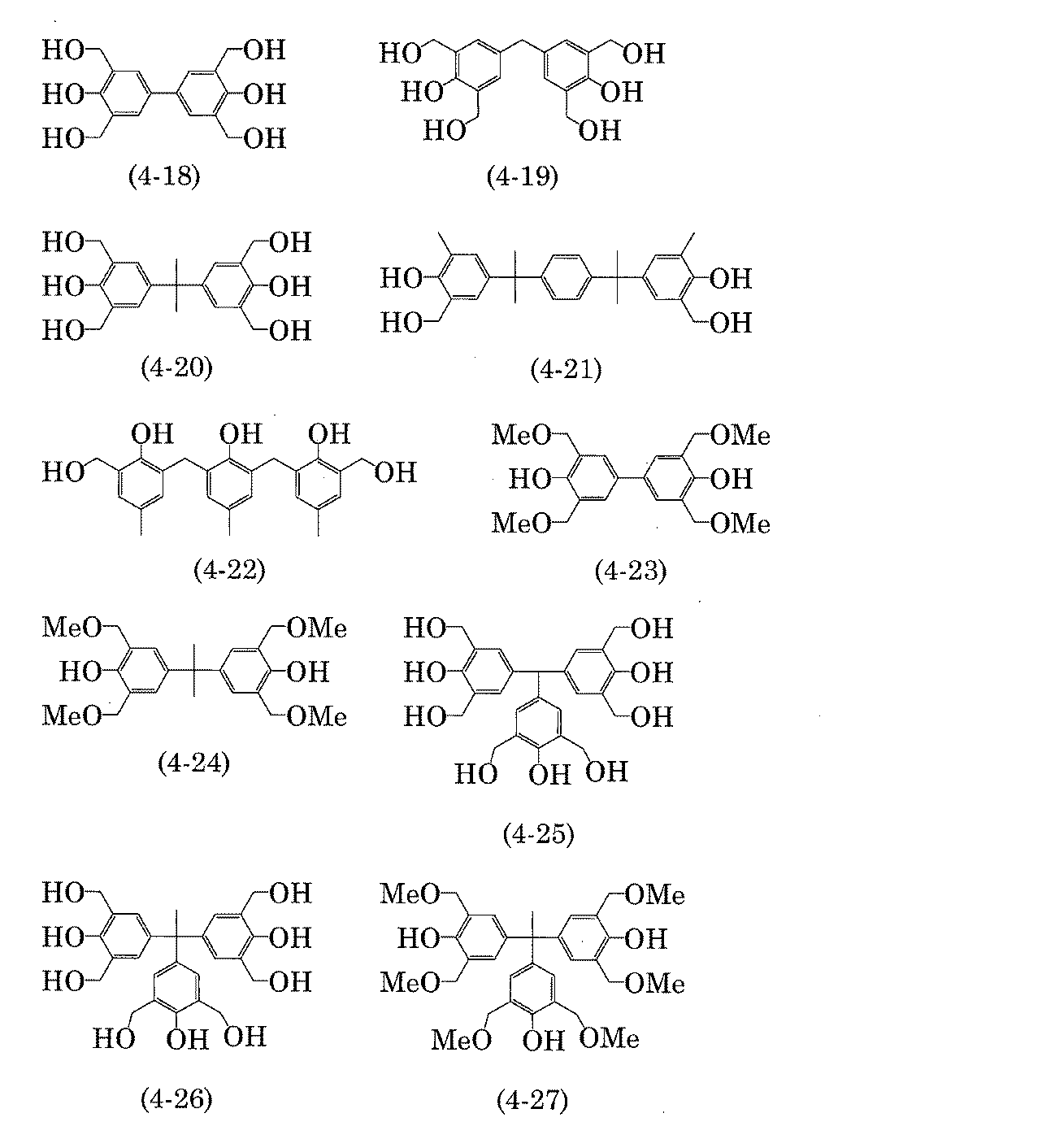
4級元素とは、例えば第四級アンモニウムカチオンが挙げられる。
本実施形態で用いられるレジストとは、フォトレジストや電子線レジストである。
次に、本実施形態のレジストパターンの形成方法について説明する。精密集積回路素子の製造に使用される基板(例えばシリコン/二酸化シリコン被覆、ガラス基板、ITO基板等の透明基板)上に、スピナー、コーター等の適当な塗布方法によりレジスト下層膜形成組成物を塗布して塗布膜を形成した後、ベークして硬化させレジスト下層膜(焼成物)を形成する。ここで、レジスト下層膜の膜厚としては、0.01μm~3.0μmが好ましい。また、塗布後にベークする条件としては、80℃~350℃で0.5分~120分間である。
本実施形態では、半導体基板上に本実施形態のレジスト下層膜形成組成物によりレジスト下層膜を形成する工程、レジスト下層膜の上にレジスト膜を形成する工程、光又は電子線照射と現像によりレジストパターンを形成する工程、形成されたレジストパターンによりレジスト下層膜をエッチングする工程、及びパターン化されたレジスト下層膜により半導体基板を加工する工程を経て半導体装置を製造することができる。
下記式(5)で表される化合物(A)としてレジスト下層膜形成組成物用の樹脂(NeoFARIT7177C-30A)(GPC(標準物質:ポリスチレン)で測定した混合割合:n=0(61%)、n=1(25%)、n=2(9%)、n=4(5%)の混合物)3.33g、下記式(4-23)で表される架橋剤(B)として3,3’,5,5’-テトラメトキシメチル-4,4’-ビスフェノール(商品名:TMOM-BP、本州化学工業(株)製)0.10g、架橋触媒としてジターシャリーブチルジフェニルヨードニウムノナフルオロメタンスルホナート(商品名:DTDPI、みどり化学(株)製)0.01g、及び界面活性剤としてフッ素系界面活性剤(商品名:R-30N、品名:メガファック、DIC(株)製)0.001gを、プロピレングリコールモノメチルエーテル6.67g及びプロピレングリコールモノメチルエーテルアセテート15.55gに溶解させ、レジスト下層膜形成組成物を調製した。


上記式(5)で表される化合物(A)としてレジスト下層膜形成組成物用の樹脂(NeoFARIT7177C-30A)3.33g、架橋剤(B)(商品名:PGME-BIP-A、ファインケム(株)製)0.10g、架橋触媒としてジターシャリーブチルジフェニルヨードニウムノナフルオロメタンスルホナート(商品名:DTDPI、みどり化学(株)製)0.01g、及び界面活性剤としてフッ素系界面活性剤(商品名:R-30N、品名:メガファック、DIC(株)製)0.001gを、プロピレングリコールモノメチルエーテル6.67g及びプロピレングリコールモノメチルエーテルアセテート15.55gに溶解させ、レジスト下層膜形成組成物を調製した。なお、架橋剤(B)として用いたPGME-BIP-Aは、下記式(3-36)で表される化合物を中心に、下記式(3-33)、下記式(3-34)及び下記式(3-35)でそれぞれ表される化合物が混合されたものである。

上記式(5)で表される化合物(A)としてレジスト下層膜形成組成物用の樹脂(NeoFARIT7177C-30A)3.33g、架橋剤(B)として3,3’,5,5’-テトラメトキシメチルー4,4’-ビスフェノール(商品名:TMOM-BP、本州化学工業(株)製)0.10g、架橋触媒として5-スルホサリチル酸0.01g、及び界面活性剤としてフッ素系界面活性剤(商品名:R-30N、品名:メガファック、DIC(株)製)0.001gを、プロピレングリコールモノメチルエーテル6.67g及びプロピレングリコールモノメチルエーテルアセテート15.55gに溶解させ、レジスト下層膜形成組成物を調製した。
上記式(5)で表される化合物(A)としてレジスト下層膜形成組成物用の樹脂(NeoFARIT7177C-30A)3.33g、架橋剤(B)として3,3’,5,5’-テトラメトキシメチルー4,4’-ビスフェノール(商品名:TMOM-BP、本州化学工業(株)製)0.10g、架橋触媒としてピリジニウムトリフルオロメタンスルホン酸0.01g、及び界面活性剤としてフッ素系界面活性剤(商品名:R-30N、品名:メガファック、DIC(株)製)0.001gを、プロピレングリコールモノメチルエーテル6.67g及びプロピレングリコールモノメチルエーテルアセテート15.55gに溶解させ、レジスト下層膜形成組成物を調製した。
上記式(5)で表される化合物(A)としてレジスト下層膜形成組成物用の樹脂(NeoFARIT7177C-30A)3.33g、架橋剤(B)として3,3’,5,5’-テトラメトキシメチルー4,4’-ビスフェノール(商品名:TMOM-BP、本州化学工業(株)製)0.10g、架橋触媒としてピリジニウムp-フェノールスルホン酸0.01g、及び界面活性剤としてフッ素系界面活性剤(商品名:R-30N、品名:メガファック、DIC(株)製)0.001gを、プロピレングリコールモノメチルエーテル6.67g及びプロピレングリコールモノメチルエーテルアセテート15.55gに溶解させ、レジスト下層膜形成組成物を調製した。
上記式(5)で表される化合物(A)としてレジスト下層膜形成組成物用の樹脂(NeoFARIT7177C-30A)3.33g、架橋剤(B)として3,3’,5,5’-テトラメトキシメチルー4,4’-ビスフェノール(商品名:TMOM-BP、本州化学工業(株)製)0.10g、架橋触媒として4級元素で一部又は全部がブロックされたトリフルオロメタンスルホン酸(商品名:K-PURE TAG-2689、King Industries社製)0.01g、及び界面活性剤としてフッ素系界面活性剤(商品名:R-30N、品名:メガファック、DIC(株)製)0.001gを、プロピレングリコールモノメチルエーテル6.67g及びプロピレングリコールモノメチルエーテルアセテート15.55gに溶解させ、レジスト下層膜形成組成物を調製した。
上記式(5)で表される化合物(A)としてレジスト下層膜形成組成物用の樹脂(NeoFARIT7177C-30A)3.33g、下記式(6)で表されるウレア化合物を基本骨格とする架橋剤(C)として1,3,4,6-テトラキス(メトキシメチル)グリコールウリル(商品名:ニカラック MX-270、三和ケミカル(株)製)0.10g、架橋触媒(D)として5-スルホサリチル酸0.01g、及び界面活性剤としてフッ素系界面活性剤(商品名:R-30N、品名:メガファック、DIC(株)製)0.001gを、プロピレングリコールモノメチルエーテル6.67g及びプロピレングリコールモノメチルエーテルアセテート15.55gに溶解させ、レジスト下層膜形成組成物を調製した。

上記式(5)で表される化合物(A)としてレジスト下層膜形成組成物用の樹脂(NeoFARIT7177C-30A)3.33g、上記式(6)で表されるウレア化合物を基本骨格とする架橋剤(C)として1,3,4,6-テトラキス(メトキシメチル)グリコールウリル(商品名:ニカラック MX-270、三和ケミカル(株)製)0.10g、架橋触媒(D)としてピリジニウムトリフルオロメタンスルホン酸0.01g、及び界面活性剤としてフッ素系界面活性剤(商品名:R-30N、品名:メガファック、DIC(株)製)0.001gを、プロピレングリコールモノメチルエーテル6.67g及びプロピレングリコールモノメチルエーテルアセテート15.55gに溶解させ、レジスト下層膜形成組成物を調製した。
上記式(5)で表される化合物(A)としてレジスト下層膜形成組成物用の樹脂(NeoFARIT7177C-30A)3.33g、上記式(6)で表されるウレア化合物を基本骨格とする架橋剤(C)として1,3,4,6-テトラキス(メトキシメチル)グリコールウリル(商品名:ニカラック MX-270、三和ケミカル(株)製)0.10g、架橋触媒(D)として下記式(7)で表されるピリジニウムp-フェノールスルホン酸0.01g、及び界面活性剤としてフッ素系界面活性剤(商品名:R-30N、品名:メガファック、DIC(株)製)0.001gを、プロピレングリコールモノメチルエーテル6.67g及びプロピレングリコールモノメチルエーテルアセテート15.55gに溶解させ、レジスト下層膜形成組成物を調製した。

上記式(5)で表される化合物(A)としてレジスト下層膜形成組成物用の樹脂(NeoFARIT7177C-30A)3.33g、上記式(6)で表されるウレア化合物を基本骨格とする架橋剤(C)として1,3,4,6-テトラキス(メトキシメチル)グリコールウリル(商品名:ニカラック MX-270、三和ケミカル(株)製)0.10g、架橋触媒(D)として4級元素で一部又は全部がブロックされたトリフルオロメタンスルホン酸(商品名:K-PURE TAG-2689、King Industries社製)0.01g、及び界面活性剤としてフッ素系界面活性剤(商品名:R-30N、品名:メガファック、DIC(株)製)0.001gを、プロピレングリコールモノメチルエーテル6.67g及びプロピレングリコールモノメチルエーテルアセテート15.55gに溶解させ、レジスト下層膜形成組成物を調製した。
上記式(5)で表される化合物(A)としてレジスト下層膜形成組成物用の樹脂(NeoFARIT7177C-30A)3.33g、上記式(6)で表されるウレア化合物を基本骨格とする架橋剤(C)として1,3,4,6-テトラキス(メトキシメチル)グリコールウリル(商品名:ニカラック MX-270、三和ケミカル(株)製)0.10g、架橋触媒としてジターシャリーブチルジフェニルヨードニウムノナフルオロメタンスルホナート(商品名:DTDPI、みどり化学(株)製)0.01g、界面活性剤としてフッ素系界面活性剤(商品名:R-30N、品名:メガファック、DIC(株)製)0.001gを、プロピレングリコールモノメチルエーテル6.67g及びプロピレングリコールモノメチルエーテルアセテート15.55gに溶解させ、レジスト下層膜形成組成物を調製した。
昇華物量の測定は国際公開第2007/111147号パンフレットに記載されている昇華物量測定装置を用いて実施した。まず、直径4インチのシリコンウェハー基板に、実施例1~実施例10、比較例1で調製したレジスト下層膜形成組成物をスピンコーターにて、膜厚50nmとなるように塗布した。レジスト下層膜が塗布されたウェハーをホットプレートが一体化した前記昇華物量測定装置にセットし、120秒間ベークし、昇華物をQCM(Quartz Crystal Microbalance)センサー、すなわち電極が形成された水晶振動子に捕集した。QCMセンサーは、水晶振動子の表面(電極)に昇華物が付着するとその質量に応じて水晶振動子の周波数が変化する(下がる)性質を利用して、微量の質量変化を測定することができる。

結果、実施例1~実施例10で調製したレジスト下層膜組成物から得られたレジスト下層膜の昇華物量比は、比較例1のレジスト下層膜形成組成物から発生する昇華物量比よりも少ない。即ち、実施例1~実施例10で適用した架橋剤や架橋触媒は、昇華物の発生量を効果的に抑制することが可能である。
Claims (8)
- (A)下記式(1)で表される化合物、及び、(B)下記式(2-1)又は下記式(2-2)で表される架橋性化合物を含むことを特徴とするレジスト下層膜形成組成物。


- (A)下記式(1)で表される化合物、
(C)架橋性化合物として、メラミン化合物、グアナミン化合物、グリコールウリル化合物、ウレア化合物、エポキシ化合物、チオエポキシ化合物、イソシアネート化合物及びアジド化合物の中から選ばれる1又は2以上の化合物、及び、
(D)架橋触媒として、p-トルエンスルホン酸、トリフルオロメタンスルホン酸、ピリジニウムp-トルエンスルホン酸、サリチル酸、5-スルホサリチル酸、4-フェノールスルホン酸、カンファースルホン酸、4-クロロベンゼンスルホン酸、ベンゼンジスルホン酸、1-ナフタレンスルホン酸、ピリジニウムトリフルオロメタンスルホン酸、ピリジニウムp-フェノールスルホン酸、クエン酸、安息香酸、ヒドロキシ安息香酸、ナフタレンカルボン酸、2,4,4,6-テトラブロモシクロヘキサジエノン、ベンゾイントシレート、2-ニトロベンジルトシレート、ピリジニウムp-トルエンスルホン酸、4級元素で一部又は全部がブロックされたトリフルオロメタンスルホン酸、4級元素で一部又は全部がブロックされたヘキサフルオロアンチモン酸、アミンで一部又は全部がブロックされたドデシルベンゼンスルホン酸、芳香族スルホニウムのヘキサフルオロリン酸塩及び芳香族スルホニウムのヘキサフルオロアンチモン酸塩の中から選ばれる1又は2以上の化合物を含むことを特徴とするレジスト下層膜形成組成物。

- さらに(E)架橋触媒を含むことを特徴とする請求項1に記載のレジスト下層膜形成組成物。
- 請求項1から請求項3の何れか1項に記載のレジスト下層膜形成組成物からなる塗布膜の焼成物であることを特徴とするレジスト下層膜。
- 請求項1から請求項3の何れか1項に記載のレジスト下層膜形成組成物を半導体基板上に塗布し焼成してレジスト下層膜を形成する工程を含み、半導体の製造に用いることを特徴とするレジストパターンの形成方法。
- 半導体基板上に請求項1から請求項3の何れか1項に記載のレジスト下層膜形成組成物によりレジスト下層膜を形成する工程と、
前記レジスト下層膜の上にレジスト膜を形成する工程と、
光又は電子線の照射と現像によりレジストパターンを形成する工程と、
形成された前記レジストパターンにより前記レジスト下層膜をエッチングする工程と、
パターン化された前記レジスト下層膜により半導体基板を加工する工程と、を含むことを特徴とする半導体装置の製造方法。 - 半導体基板上に請求項1から請求項3の何れか1項に記載のレジスト下層膜形成組成物によりレジスト下層膜を形成する工程と、
前記レジスト下層膜の上にハードマスクを形成する工程と、
前記ハードマスクの上にレジスト膜を形成する工程と、
光又は電子線の照射と現像によりレジストパターンを形成する工程と、
形成された前記レジストパターンにより前記ハードマスクをエッチングする工程と、
パターン化された前記ハードマスクにより前記レジスト下層膜をエッチングする工程と、
パターン化された前記レジスト下層膜により半導体基板を加工する工程と、を含むことを特徴とする半導体装置の製造方法。 - 前記ハードマスクは、無機物の塗布又は無機物の蒸着により形成されたものであることを特徴とする請求項7に記載の半導体装置の製造方法。
Priority Applications (6)
| Application Number | Priority Date | Filing Date | Title |
|---|---|---|---|
| KR1020207003740A KR102612701B1 (ko) | 2017-07-14 | 2018-07-12 | 레지스트 하층막 형성 조성물, 레지스트 하층막, 레지스트 패턴의 형성방법 및 반도체장치의 제조방법 |
| CN201880045397.2A CN110832397B (zh) | 2017-07-14 | 2018-07-12 | 抗蚀剂下层膜形成用组合物、抗蚀剂下层膜、及抗蚀剂图案的形成方法 |
| JP2019529787A JP7368791B2 (ja) | 2017-07-14 | 2018-07-12 | レジスト下層膜形成組成物、レジスト下層膜、レジストパターンの形成方法及び半導体装置の製造方法 |
| US16/631,011 US11169441B2 (en) | 2017-07-14 | 2018-07-12 | Composition for forming resist underlayer film, resist underlayer film, method for forming resist pattern and method for producing semiconductor device |
| JP2023173912A JP2024001186A (ja) | 2017-07-14 | 2023-10-05 | レジスト下層膜形成組成物、レジスト下層膜、レジストパターンの形成方法及び半導体装置の製造方法 |
| JP2023173911A JP2024001185A (ja) | 2017-07-14 | 2023-10-05 | レジスト下層膜形成組成物、レジスト下層膜、レジストパターンの形成方法及び半導体装置の製造方法 |
Applications Claiming Priority (2)
| Application Number | Priority Date | Filing Date | Title |
|---|---|---|---|
| JP2017-138499 | 2017-07-14 | ||
| JP2017138499 | 2017-07-14 |
Publications (1)
| Publication Number | Publication Date |
|---|---|
| WO2019013293A1 true WO2019013293A1 (ja) | 2019-01-17 |
Family
ID=65002456
Family Applications (1)
| Application Number | Title | Priority Date | Filing Date |
|---|---|---|---|
| PCT/JP2018/026361 WO2019013293A1 (ja) | 2017-07-14 | 2018-07-12 | レジスト下層膜形成組成物、レジスト下層膜、レジストパターンの形成方法及び半導体装置の製造方法 |
Country Status (6)
| Country | Link |
|---|---|
| US (1) | US11169441B2 (ja) |
| JP (3) | JP7368791B2 (ja) |
| KR (1) | KR102612701B1 (ja) |
| CN (1) | CN110832397B (ja) |
| TW (1) | TWI817950B (ja) |
| WO (1) | WO2019013293A1 (ja) |
Cited By (4)
| Publication number | Priority date | Publication date | Assignee | Title |
|---|---|---|---|---|
| KR20210113909A (ko) * | 2020-03-09 | 2021-09-17 | 삼성에스디아이 주식회사 | 하드마스크 조성물 및 패턴 형성 방법 |
| JPWO2021241680A1 (ja) * | 2020-05-27 | 2021-12-02 | ||
| WO2022065374A1 (ja) * | 2020-09-28 | 2022-03-31 | 日産化学株式会社 | フルオロアルキル基を有する有機酸またはその塩を含むレジスト下層膜形成組成物 |
| WO2022176571A1 (ja) * | 2021-02-16 | 2022-08-25 | 三菱瓦斯化学株式会社 | 樹脂、組成物、レジストパターン形成方法、回路パターン形成方法及び樹脂の精製方法 |
Families Citing this family (1)
| Publication number | Priority date | Publication date | Assignee | Title |
|---|---|---|---|---|
| JP7445583B2 (ja) * | 2020-11-25 | 2024-03-07 | 信越化学工業株式会社 | レジスト下層膜材料、パターン形成方法、及びレジスト下層膜形成方法 |
Citations (8)
| Publication number | Priority date | Publication date | Assignee | Title |
|---|---|---|---|---|
| JP2008546009A (ja) * | 2005-05-27 | 2008-12-18 | チェイル インダストリーズ インコーポレイテッド | 反射防止ハードマスク組成物およびその使用方法 |
| JP2012214720A (ja) * | 2011-03-28 | 2012-11-08 | Shin-Etsu Chemical Co Ltd | ビフェニル誘導体、レジスト下層膜材料、レジスト下層膜形成方法及びパターン形成方法 |
| WO2014208542A1 (ja) * | 2013-06-26 | 2014-12-31 | 日産化学工業株式会社 | 置換された架橋性化合物を含むレジスト下層膜形成組成物 |
| WO2016072316A1 (ja) * | 2014-11-04 | 2016-05-12 | 日産化学工業株式会社 | アリーレン基を有するポリマーを含むレジスト下層膜形成組成物 |
| WO2016147989A1 (ja) * | 2015-03-13 | 2016-09-22 | 三菱瓦斯化学株式会社 | 化合物、樹脂、リソグラフィー用下層膜形成材料、リソグラフィー用下層膜形成用組成物、リソグラフィー用下層膜、パターン形成方法、及び、化合物又は樹脂の精製方法 |
| WO2016158457A1 (ja) * | 2015-03-30 | 2016-10-06 | 三菱瓦斯化学株式会社 | 化合物、樹脂、及びそれらの精製方法、リソグラフィー用の下層膜形成材料、下層膜形成用組成物、及び下層膜、並びに、レジストパターン形成方法、及び回路パターン形成方法 |
| JP2016206676A (ja) * | 2015-04-24 | 2016-12-08 | Jsr株式会社 | レジスト下層膜形成方法及びパターン形成方法 |
| WO2017069063A1 (ja) * | 2015-10-19 | 2017-04-27 | 日産化学工業株式会社 | 長鎖アルキル基含有ノボラックを含むレジスト下層膜形成組成物 |
Family Cites Families (2)
| Publication number | Priority date | Publication date | Assignee | Title |
|---|---|---|---|---|
| WO2014024836A1 (ja) * | 2012-08-10 | 2014-02-13 | 日産化学工業株式会社 | レジスト下層膜形成組成物 |
| SG11201706524WA (en) * | 2015-03-06 | 2017-09-28 | Mitsubishi Gas Chemical Co | Compound, resin, material for forming underlayer film for lithography, underlayer film for lithography, pattern forming method, and method for purifying compound or resin |
-
2018
- 2018-07-12 CN CN201880045397.2A patent/CN110832397B/zh active Active
- 2018-07-12 KR KR1020207003740A patent/KR102612701B1/ko active IP Right Grant
- 2018-07-12 WO PCT/JP2018/026361 patent/WO2019013293A1/ja active Application Filing
- 2018-07-12 JP JP2019529787A patent/JP7368791B2/ja active Active
- 2018-07-12 US US16/631,011 patent/US11169441B2/en active Active
- 2018-07-13 TW TW107124218A patent/TWI817950B/zh active
-
2023
- 2023-10-05 JP JP2023173911A patent/JP2024001185A/ja active Pending
- 2023-10-05 JP JP2023173912A patent/JP2024001186A/ja active Pending
Patent Citations (8)
| Publication number | Priority date | Publication date | Assignee | Title |
|---|---|---|---|---|
| JP2008546009A (ja) * | 2005-05-27 | 2008-12-18 | チェイル インダストリーズ インコーポレイテッド | 反射防止ハードマスク組成物およびその使用方法 |
| JP2012214720A (ja) * | 2011-03-28 | 2012-11-08 | Shin-Etsu Chemical Co Ltd | ビフェニル誘導体、レジスト下層膜材料、レジスト下層膜形成方法及びパターン形成方法 |
| WO2014208542A1 (ja) * | 2013-06-26 | 2014-12-31 | 日産化学工業株式会社 | 置換された架橋性化合物を含むレジスト下層膜形成組成物 |
| WO2016072316A1 (ja) * | 2014-11-04 | 2016-05-12 | 日産化学工業株式会社 | アリーレン基を有するポリマーを含むレジスト下層膜形成組成物 |
| WO2016147989A1 (ja) * | 2015-03-13 | 2016-09-22 | 三菱瓦斯化学株式会社 | 化合物、樹脂、リソグラフィー用下層膜形成材料、リソグラフィー用下層膜形成用組成物、リソグラフィー用下層膜、パターン形成方法、及び、化合物又は樹脂の精製方法 |
| WO2016158457A1 (ja) * | 2015-03-30 | 2016-10-06 | 三菱瓦斯化学株式会社 | 化合物、樹脂、及びそれらの精製方法、リソグラフィー用の下層膜形成材料、下層膜形成用組成物、及び下層膜、並びに、レジストパターン形成方法、及び回路パターン形成方法 |
| JP2016206676A (ja) * | 2015-04-24 | 2016-12-08 | Jsr株式会社 | レジスト下層膜形成方法及びパターン形成方法 |
| WO2017069063A1 (ja) * | 2015-10-19 | 2017-04-27 | 日産化学工業株式会社 | 長鎖アルキル基含有ノボラックを含むレジスト下層膜形成組成物 |
Cited By (7)
| Publication number | Priority date | Publication date | Assignee | Title |
|---|---|---|---|---|
| KR20210113909A (ko) * | 2020-03-09 | 2021-09-17 | 삼성에스디아이 주식회사 | 하드마스크 조성물 및 패턴 형성 방법 |
| KR102456164B1 (ko) | 2020-03-09 | 2022-10-17 | 삼성에스디아이 주식회사 | 하드마스크 조성물 및 패턴 형성 방법 |
| JPWO2021241680A1 (ja) * | 2020-05-27 | 2021-12-02 | ||
| WO2021241680A1 (ja) * | 2020-05-27 | 2021-12-02 | 国立大学法人 東京大学 | 熱硬化性樹脂の超薄膜 |
| JP7473993B2 (ja) | 2020-05-27 | 2024-04-24 | 国立大学法人 東京大学 | 熱硬化性樹脂の超薄膜 |
| WO2022065374A1 (ja) * | 2020-09-28 | 2022-03-31 | 日産化学株式会社 | フルオロアルキル基を有する有機酸またはその塩を含むレジスト下層膜形成組成物 |
| WO2022176571A1 (ja) * | 2021-02-16 | 2022-08-25 | 三菱瓦斯化学株式会社 | 樹脂、組成物、レジストパターン形成方法、回路パターン形成方法及び樹脂の精製方法 |
Also Published As
| Publication number | Publication date |
|---|---|
| JPWO2019013293A1 (ja) | 2020-05-07 |
| TW201908273A (zh) | 2019-03-01 |
| TWI817950B (zh) | 2023-10-11 |
| US11169441B2 (en) | 2021-11-09 |
| KR102612701B1 (ko) | 2023-12-12 |
| JP2024001186A (ja) | 2024-01-09 |
| US20200142310A1 (en) | 2020-05-07 |
| CN110832397B (zh) | 2023-12-15 |
| JP2024001185A (ja) | 2024-01-09 |
| CN110832397A (zh) | 2020-02-21 |
| KR20200030080A (ko) | 2020-03-19 |
| JP7368791B2 (ja) | 2023-10-25 |
Similar Documents
| Publication | Publication Date | Title |
|---|---|---|
| JP6593616B2 (ja) | 置換された架橋性化合物を含むレジスト下層膜形成組成物 | |
| US11720024B2 (en) | Resist underlayer film-forming composition containing indolocarbazole novolak resin | |
| JP6974799B2 (ja) | 膜密度が向上したレジスト下層膜を形成するための組成物 | |
| JP7368791B2 (ja) | レジスト下層膜形成組成物、レジスト下層膜、レジストパターンの形成方法及び半導体装置の製造方法 | |
| JP6124025B2 (ja) | 多核フェノール類を有するノボラック樹脂を含むレジスト下層膜形成組成物 | |
| US11300879B2 (en) | Resist underlayer film forming composition containing triaryldiamine-containing novolac resin | |
| JP2021157184A (ja) | 長鎖アルキル基含有ノボラックを含むレジスト下層膜形成組成物 | |
| JP7265225B2 (ja) | 芳香族ビニル化合物が付加したトリアリールジアミン含有ノボラック樹脂を含むレジスト下層膜形成組成物 |
Legal Events
| Date | Code | Title | Description |
|---|---|---|---|
| 121 | Ep: the epo has been informed by wipo that ep was designated in this application |
Ref document number: 18832271 Country of ref document: EP Kind code of ref document: A1 |
|
| ENP | Entry into the national phase |
Ref document number: 2019529787 Country of ref document: JP Kind code of ref document: A |
|
| NENP | Non-entry into the national phase |
Ref country code: DE |
|
| ENP | Entry into the national phase |
Ref document number: 20207003740 Country of ref document: KR Kind code of ref document: A |
|
| 122 | Ep: pct application non-entry in european phase |
Ref document number: 18832271 Country of ref document: EP Kind code of ref document: A1 |