WO2019013166A1 - 撮像素子、電子機器および撮像素子の製造方法 - Google Patents
撮像素子、電子機器および撮像素子の製造方法 Download PDFInfo
- Publication number
- WO2019013166A1 WO2019013166A1 PCT/JP2018/025890 JP2018025890W WO2019013166A1 WO 2019013166 A1 WO2019013166 A1 WO 2019013166A1 JP 2018025890 W JP2018025890 W JP 2018025890W WO 2019013166 A1 WO2019013166 A1 WO 2019013166A1
- Authority
- WO
- WIPO (PCT)
- Prior art keywords
- light
- light emitting
- light receiving
- substrate
- imaging device
- Prior art date
- Legal status (The legal status is an assumption and is not a legal conclusion. Google has not performed a legal analysis and makes no representation as to the accuracy of the status listed.)
- Ceased
Links
Images





Classifications
-
- G—PHYSICS
- G06—COMPUTING OR CALCULATING; COUNTING
- G06T—IMAGE DATA PROCESSING OR GENERATION, IN GENERAL
- G06T1/00—General purpose image data processing
-
- H—ELECTRICITY
- H04—ELECTRIC COMMUNICATION TECHNIQUE
- H04N—PICTORIAL COMMUNICATION, e.g. TELEVISION
- H04N1/00—Scanning, transmission or reproduction of documents or the like, e.g. facsimile transmission; Details thereof
- H04N1/024—Details of scanning heads ; Means for illuminating the original
- H04N1/028—Details of scanning heads ; Means for illuminating the original for picture information pick-up
-
- H—ELECTRICITY
- H04—ELECTRIC COMMUNICATION TECHNIQUE
- H04N—PICTORIAL COMMUNICATION, e.g. TELEVISION
- H04N25/00—Circuitry of solid-state image sensors [SSIS]; Control thereof
- H04N25/70—SSIS architectures; Circuits associated therewith
-
- H—ELECTRICITY
- H04—ELECTRIC COMMUNICATION TECHNIQUE
- H04N—PICTORIAL COMMUNICATION, e.g. TELEVISION
- H04N25/00—Circuitry of solid-state image sensors [SSIS]; Control thereof
- H04N25/70—SSIS architectures; Circuits associated therewith
- H04N25/76—Addressed sensors, e.g. MOS or CMOS sensors
- H04N25/77—Pixel circuitry, e.g. memories, A/D converters, pixel amplifiers, shared circuits or shared components
-
- H—ELECTRICITY
- H10—SEMICONDUCTOR DEVICES; ELECTRIC SOLID-STATE DEVICES NOT OTHERWISE PROVIDED FOR
- H10F—INORGANIC SEMICONDUCTOR DEVICES SENSITIVE TO INFRARED RADIATION, LIGHT, ELECTROMAGNETIC RADIATION OF SHORTER WAVELENGTH OR CORPUSCULAR RADIATION
- H10F39/00—Integrated devices, or assemblies of multiple devices, comprising at least one element covered by group H10F30/00, e.g. radiation detectors comprising photodiode arrays
- H10F39/10—Integrated devices
- H10F39/12—Image sensors
-
- H—ELECTRICITY
- H10—SEMICONDUCTOR DEVICES; ELECTRIC SOLID-STATE DEVICES NOT OTHERWISE PROVIDED FOR
- H10F—INORGANIC SEMICONDUCTOR DEVICES SENSITIVE TO INFRARED RADIATION, LIGHT, ELECTROMAGNETIC RADIATION OF SHORTER WAVELENGTH OR CORPUSCULAR RADIATION
- H10F55/00—Radiation-sensitive semiconductor devices covered by groups H10F10/00, H10F19/00 or H10F30/00 being structurally associated with electric light sources and electrically or optically coupled thereto
-
- H—ELECTRICITY
- H10—SEMICONDUCTOR DEVICES; ELECTRIC SOLID-STATE DEVICES NOT OTHERWISE PROVIDED FOR
- H10H—INORGANIC LIGHT-EMITTING SEMICONDUCTOR DEVICES HAVING POTENTIAL BARRIERS
- H10H29/00—Integrated devices, or assemblies of multiple devices, comprising at least one light-emitting semiconductor element covered by group H10H20/00
- H10H29/10—Integrated devices comprising at least one light-emitting semiconductor component covered by group H10H20/00
Definitions
- the present invention relates to an imaging device, an electronic device, and a method of manufacturing an imaging device used for biometric authentication and the like.
- the imaging device includes a light receiving unit in which a plurality of light receiving elements for receiving light from an object are arranged in a first direction on a substrate and a second direction intersecting the first direction.
- a light emitting element for emitting light between the light receiving element of the light receiving unit and the light receiving element is provided on the light emitting unit where a plurality of light emitting units are arranged in the second direction on the substrate and each light emitting element of the light emitting unit And a light guiding member for guiding light from the light emitting unit to the object.
- An electronic device includes the imaging device of the first aspect.
- a plurality of light receiving elements are provided in a predetermined area of a substrate, and a wiring layer is formed on the substrate provided with the light receiving elements. And exposing the upper surface of the light receiving element of the substrate after the substrate and the wiring layer are turned upside down, and providing the light emitting element between the light receiving element and the light receiving element of the substrate. Forming a light transmitting member on the substrate provided with the light receiving element and the light emitting element; and forming a micro lens and a light guiding member on the light transmitting member.
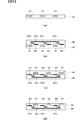
- FIG. 6 (a) to 6 (d) are diagrams for explaining an example of the manufacturing procedure of the imaging device.
- FIGS. 7A to 7D are diagrams for explaining an example of the manufacturing procedure of the imaging device. It is a schematic diagram which shows the cross section of the image pick-up element by 2nd Embodiment. It is the schematic diagram which looked at the image pick-up element diagonally. It is a schematic diagram which shows the cross section of the image pick-up element by 3rd Embodiment.
- FIG. 1 is a diagram illustrating a biometric authentication apparatus 10 for imaging a fingerprint for biometric authentication.
- the biometric authentication device 10 may be incorporated into the ATM, the mobile device, etc., or connected to the ATM, the mobile device, etc.
- the cover glass 500 of the imaging device 1 (FIG. 2), which will be described in detail later, is exposed at the position of the sensor window 20 of the biometric device 10.
- the user touches the sensor window 20 with a finger 30 to receive fingerprint authentication. Since the biometric authentication technology is known, the description of the biometric authentication technology is omitted, and the configuration of the imaging device 1 built in the biometric authentication device 10 will be mainly described.
- the biometric authentication device 10 of a size suitable for capturing a fingerprint is illustrated in FIG. 1, the biometric authentication device 10 having an imaging element 1 of a size suitable for palm print authentication, vein pattern authentication, etc. You may
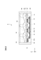
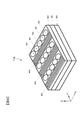
- FIG. 2 is a schematic view showing a cross section of the imaging device 1 incorporated in the biometric device 10.
- FIG. 3 is a block diagram for explaining a schematic configuration of the imaging device 1 of FIG.
- XYZ axes constituting a right-handed coordinate system orthogonal to one another are defined, and in the following several drawings, the orientations of the respective drawings are illustrated with reference to the XYZ axes of FIG. In the case of FIG.
- the front side of the sheet is the X axis plus direction
- the right side of the sheet orthogonal to the X axis is the Y axis plus direction
- the sheet upper direction orthogonal to the X axis and the Y axis is the Z axis plus direction.
- the imaging device 1 is a so-called contact type two-dimensional image sensor.
- the imaging device 1 includes, for example, a substrate 100 which is a semiconductor substrate of single crystal silicon, a wiring layer 200 formed on the back surface (Z-axis minus direction), and a transparent electrode formed on the surface (Z-axis plus direction) of the substrate 100 300 and a transparent layer 400 formed on the surface of the transparent electrode 300 (Z-axis plus direction), and hermetically sealed by a cover glass 500 and a sealing body 600.
- a plurality of photodiodes 101 and a plurality of light emitting elements 102 are formed in the substrate 100.
- the plurality of photodiodes 101 are two-dimensionally arranged in the X-axis direction (row direction) and the Y-axis direction (column direction) as shown in FIG.
- a plurality of (for example, four) photodiodes 101 are arranged discretely in the X-axis direction (row direction) of the substrate 100 (FIG. 2) and are discretely arranged.
- a plurality of sets (for example, four sets) of photodiodes 101 are arranged in the Y-axis direction (column direction) of the substrate 100 (FIG. 2).
- the light emitting elements 102 are extended in a rectangular shape long in the X axis direction (row direction) of the substrate 100, and the discretely arranged photodiodes 101 and the discretely arranged photodiodes 101 are arranged.
- the discretely arranged photodiodes 101 and the discretely arranged photodiodes 101 are arranged.
- CMOS Complementary Metal Oxide Semiconductor
- Each light emitting element 102 is connected to the light emitting element control circuit 107. This connection is made via the electrode 202 and the wiring 201c (FIG. 3) provided in the wiring layer 200 of FIG.
- the light emitting element 102 is controlled to be turned on and off by the light emitting element control circuit 107 in each X-axis direction (row direction) of the substrate 100.
- Each pixel of the imaging device 1 is configured by several semiconductor elements as referred to as known four transistors or three transistors. Briefly describing the case of four transistors per pixel, each pixel includes a transfer transistor that transfers the charge generated by the photodiode 101 to the floating diffusion, and a reset transistor for resetting the charge of the photodiode 101 and the floating diffusion. And an amplification transistor for amplifying a signal based on the charge, and a row selection transistor for connecting an output of the amplification transistor to a corresponding wiring 201a. In the example of FIG. 3, only the semiconductor switch 103a functioning as a row selection transistor in each pixel is illustrated, and the other semiconductor elements are not illustrated. In the case of three transistors, the transfer transistor among the four transistors is omitted.
- the wiring 201 d corresponds to the horizontal read signal line connected to the output terminal 108.
- the wirings 201a in each column corresponding to the vertical read signal line are connected to the wiring 201d through the semiconductor switch 103b functioning as a column selection transistor.
- the transparent electrode 300 formed on the surface (Z-axis plus direction) of the substrate 100 in FIG. 2 is formed of, for example, indium tin oxide (ITO), and functions as a common electrode of the light emitting element 102. Further, in the wiring layer 200, the individual electrodes 202 are formed for the respective light emitting elements 102.
- the aforementioned light emitting element control circuit 107 (FIG. 3) controls the light emission of each light emitting element 102 through the corresponding individual electrode 202.
- a transparent layer 400 is formed on the upper surface (Z-axis plus direction) of the transparent electrode 300.
- the transparent layer 400 is formed of, for example, a transparent resin.
- the microlens 401 and the inclined surface 402 are formed by processing the shape of the transparent layer 400.
- Microlenses 401 are formed on the transparent layer 400 at positions above the respective photodiodes 101.
- the micro lens 401 forms a real image of an object (a fingerprint of the finger 30 in the example of FIG. 1) located on the upper surface (Z-axis plus direction) of the cover glass 500 on the light receiving surface of the photodiode 101. That is, the shape and refractive index of the micro lens 401 are adjusted so that a real image of the contact surface of the object in contact with the upper surface of the cover glass 500 is formed on the light receiving surface of the photodiode 101.
- light from each portion of the contact surface of the object in contact with the cover glass 500 is appropriately condensed and received by the corresponding photodiode 101.
- each photodiode 101 receives light from a portion of the object in contact with the cover glass 500 above (the Z-axis plus direction) the photodiode 101.
- a slope 402 is provided on the transparent layer 400 on the light emitting element 102 in FIG.
- the light beam output from the light emitting element 102 is refracted by the slope 402 so that the light emitting element 102 illuminates the portion of the cover glass 500 above the photodiode 101 disposed next to the light emitting element 102. That is, the inclination angle and the refractive index of the slope 402 are adjusted to illuminate the portion of the cover glass 500 above the photodiode 101 disposed next to the light emitting element 102.
- the imaging device 1 described above is hermetically sealed by the sealing body 600 and the cover glass 500 by a known method.
- FIG. 4 is a schematic view of the imaging device 1 as viewed obliquely.
- FIG. 4 mainly illustrates the configuration of the transparent layer 400, and the cover glass 500, the sealing body 600, and the like of FIG. 2 are omitted.
- a plurality of microlenses are provided at positions on a plurality of photodiodes 101 (FIG. 2) constituting pixels.
- 401 is formed.
- slopes 402 are formed between the rows of the plurality of microlenses 401.
- the slope 402 is inclined such that the height in the Z-axis direction decreases as it goes in the negative Y-axis direction.
- the inclined surface 402 directs light from the light emitting element 102 (FIG. 2) to the cover glass 500 (FIG. 2) on the photodiode 101 (FIG. 2) disposed next to the light emitting element 102. That is, the inclined surface 402 bends a light beam output from the light emitting element 102 (FIG. 2) and traveling in the Z-axis plus direction toward the photodiode 101 (FIG. 2) disposed next to the light emitting element 102.
- the operation of the imaging device 1 will be briefly described.
- the object to be imaged the fingerprint of the finger 30 in the example of FIG. 1 contacts the upper surface (the Z-axis plus direction) of the cover glass 500. Since the area of the cover glass 500 in contact with the object is shielded, the amount of light incident on the light receiving surface of the photodiode 101 from the outside of the imaging device 1 through the cover glass 500 is reduced.
- the imaging device 1 is configured to start an imaging operation, for example, when the amount of light received by the plurality of photodiodes 101 becomes lower than a predetermined value.
- the light emitting element control circuit 107 (FIG. 3) causes the plurality of light emitting elements 102 to sequentially emit light.
- the light emitted from each light emitting element 102 is refracted by the slope 402 (FIG. 2) on each light emitting element 102, and a cover glass 500 on a plurality of photodiodes 101 arranged in a row next to each light emitting element 102. It illuminates the part of the object located on the upper surface (Z-axis plus direction) of
- the light reflected by the illuminated part of the object passes through the cover glass 500 and enters the imaging element 1 again.
- the light entering the imaging element 1 is received by the photodiode 101 below the microlens 401 via the microlens 401.
- the image pickup device 1 picks up a real image at the same magnification of the object to be picked up in contact with the upper surface of the cover glass 500.
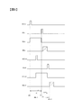
- FIG. 5 is a diagram for explaining the timing of the imaging operation by the imaging device 1. Since the imaging device 1 is a CMOS image sensor, an exposure operation and a readout operation are performed for each row of the photodiodes 101 (arrangement in the X-axis direction in FIG. 3) that constitute a pixel.
- the timing chart of FIG. 5 shows operations of the photodiodes 101 in the n-th row and the n + 1-th row, and the light emitting element 102 corresponding to the n-th row and the n + 1-th row.
- the row control circuit 104 (FIG. 3) supplies the row selection pulse for the nth row to the row selection transistor (semiconductor switch 103a) via the wiring 201b to turn on the row selection transistor (semiconductor switch 103a).
- the row control circuit 104 (FIG. 3) supplies the reset pulse RSTn for each photodiode 101 in the n-th row to the reset transistor (not shown) via the wiring 201b.
- the reset transistor is turned on to reset the charges accumulated in the n-th photodiodes 101 and the corresponding floating diffusions.
- the light emitting element control circuit 107 changes the light emitting element control signal ILLn for the light emitting element 102 in the nth row to the H level via the wiring 201c.
- the light emitting element 102 in the nth row is turned on.
- the illumination light from the n-th row of light emitting elements 102 is refracted by the slope 402 of the transparent layer 400 (FIG. 2) described above, and the portion of the object on the cover glass 500 above the n-th row of photodiodes Light up.
- the light reflected from the illuminated part of the object is incident on the photodiode 101 through the microlens 401.
- the row control circuit 104 (FIG. 3) supplies the transfer pulse TRn for the pixel in the nth row to the transfer transistor (not shown) via the wiring 201b.
- the transfer pulse TRn for the pixel in the nth row to the transfer transistor (not shown) via the wiring 201b.
- the light-emitting element control circuit 107 sets the light-emitting element control signal ILLn for the n-th light emitting element 102 to the L level through the wiring 201c. As a result, the light emitting element 102 in the nth row is extinguished.
- the time Tn from the time t0n to the time t1n at which the light emitting element 102 in the nth row is lit is the exposure time of the photodiode 101 in the nth row. That is, the control of the exposure time of the photodiode 101 in the nth row can be performed by the control of the lighting time of the light emitting element 102 in the nth row.
- the column control circuit 105 (FIG. 3) sequentially supplies the read pulse ROn to the semiconductor switches 103 b (column select transistors) in each column at time t2n.
- an amplification signal based on the charge transferred to the floating diffusion in the n-th row is sequentially read out from the output terminal 108 through the wiring 201 a and the wiring 201 d of the column selected by the semiconductor switch 103 b.
- the image data of the object can be obtained by repeating the same operation and performing the exposure operation and the reading operation for all the rows of the imaging device 1.
- the supply of the row selection pulse to the (n + 1) th row, the supply of the reset pulse RSTn + 1, the supply of the transfer pulse TRn + 1, and the control timing of the light emitting element control signal ILLn + 1 to the light emitting element 102 are also shifted backward by the readout time by the readout pulse ROn. It becomes a thing. This is so-called rolling readout in which the subsequent readout is also sequentially shifted.
- the exposure time Tn + 1 may basically be the same as Tn, the exposure time Tn + 1 may be changed row by row in consideration of variations in the characteristics of the light emitting element 102 and the like.
- FIG. 6A for example, at predetermined positions of a silicon substrate 100, peripheral elements such as a photodiode 101 forming each pixel, a floating diffusion, and a transistor are formed using a known method. In FIGS. 6 and 7, the floating diffusion, the transistor, and the like are not shown.
- the wiring layer 200 is formed on the silicon substrate 100 using a known method.
- wirings 201a, 201b, 201c, and 201d for inputting and outputting control signals for driving the imaging device 1 and signals generated by the imaging device 1 are formed in multiple layers.
- an electrode 202 for the light emitting element 102 described later is formed in the lowermost layer of the wiring layer 200.
- the wirings 201 c and 201 d are not shown.
- the upper and lower sides of the silicon substrate 100 are reversed.
- the electrode 202 is located in the upper layer of the wiring layer 200 by reversing the upper limit.
- the silicon substrate 100 is scraped from the upper surface of the silicon substrate 100 by a method such as chemical etching until the light receiving surface of the photodiode 101 appears on the surface.
- the region of the silicon substrate 100 corresponding to the electrode 202 for the light emitting element 102 is selectively removed by using a method such as photolithography to expose the light emitting electrode 202.
- the light emitting element 102 is formed in the region from which the silicon substrate 100 is removed. Since the electrode 202 is provided in advance, post-processing can be simplified.
- the light emitting element 102 is, for example, a light emitting diode (LED) using a compound semiconductor or an organic EL (electroluminescence).
- LED light emitting diode
- organic EL electroluminescence
- crystal growth using evaporation, evaporation, sputtering, printing, or the like can be used as appropriate.
- the imaging element 1 can be thinner compared to the case where the light emitting layer is stacked on the photodiode 101. It can be configured.
- the transparent electrode 300 is formed on the silicon substrate 100 and the light emitting element 102.
- the transparent electrode 300 uses indium tin oxide (ITO) or the like as described above. As described above, the transparent electrode 300 is used as a common electrode of the light emitting element 102 in this embodiment.
- ITO indium tin oxide
- the transparent layer 400 is formed on the transparent electrode 300. Furthermore, in the transparent layer 400, the microlenses 401 are formed on the plurality of photodiodes 101 that constitute a pixel. Further, a slope 402 is formed over the light emitting element 102.
- the micro lenses 401 and the slopes 402 may be formed by forming the transparent layer 400 and then molding the resultant by embossing, or bonding the transparent layer 400 formed by casting polymerization or the like in advance to the upper surface of the transparent electrode 300. May be.
- the photodiode 101 receiving light from an object to be imaged (the finger 30 in the above example) is in the X-axis direction (row direction) and the Y-axis direction (column direction) on the substrate 100
- a plurality of light receiving portions (generally referred to as a plurality of photodiodes 101) respectively arranged in plural, and a light emitting element 102 emitting light between the photodiodes 101 and the photodiodes 101 of the light receiving portion
- a plurality of light emitting units (generally referred to as a plurality of light emitting elements 102) arranged in the column direction), and slopes 402 provided on the light emitting elements 102 of the light emitting units and guiding light from the light emitting units to an object are provided.
- the imaging device 1 can be thinner than in the case where the light receiving unit and the light emitting unit are stacked.
- the finger 30 is appropriately illuminated, and the light reflected by the finger 30 is received by the photodiode 101 of the light receiving unit. it can.
- the imaging device 1 can appropriately capture an image of the finger 30 (fingerprint).
- each light emitting element 102 of the light emitting unit is extended in a rectangular shape long in the X axis direction (row direction) on the substrate 100
- the plurality of photodiodes 101 arranged in the (direction) and the light emitting elements 102 of the light emitting portion are alternately arranged in the Y axis direction (the column direction) on the substrate 100. Since the light emitting elements 102 of the light emitting portion are formed in a rectangular shape long in the X-axis direction (row direction) on the substrate 100, the light emitting portions can be divided into rows and lighting and extinguishing can be controlled. With this configuration, for example, the light emitting elements 102 can be lighted in order according to the timing of imaging by the plurality of photodiodes 101 arranged in the X axis direction (row direction) of the light receiving unit.
- the slope 402 bends the light emitted from the light emitting element 102 toward the photodiode 101 disposed next to the light emitting element 102.
- the light emitted from the light emitting element 102 of the light emitting unit is placed in the X axis direction (row direction) next to the light emitting element 102 of the photodiodes 101 in the light receiving unit. It can be properly guided to the finger 30 to be imaged.
- each photodiode 101 of the light receiving unit receives light reflected by different portions of the finger 30, the imaging device 1 is a finger 30 (fingerprint Can be properly captured.
- the microlens 401 is provided in each of the photodiodes 101 of the light receiving unit and condenses the reflected light of the object onto the photodiode 101.
- the image can be bright and high quality as compared with.
- the transparent layer 400 is provided on the top surface of the light receiving unit and the light emitting unit, and the slope 402 and the micro lens 401 are formed on the transparent layer 400.
- the manufacturing becomes easier, and the manufacturing cost can be reduced.
- the light receiving unit captures an equal-magnification image of an object in contact with the cover glass 500 provided closer to the object than the transparent layer 400. Since it comprised in this way, the image pick-up element 1 suitable for biometric authentication, such as a fingerprint, can be obtained.
- the method of manufacturing the imaging device 1 includes the steps of providing a plurality of photodiodes 101 in a predetermined region of the substrate 100, forming the wiring layer 200 on the substrate 100 provided with the photodiodes 101, the substrate 100 and the wiring layer An etching process for exposing the upper surface of the photodiode 101 of the substrate 100 after turning upside down 200, a process of providing the light emitting element 102 between the photodiode 101 and the photodiode 101 of the substrate 100, a photodiode 101 and a light emitting element 102 And the step of forming the microlenses 401 and the sloped surface 402 on the light transmitting member 400. Since it comprised in this way, since a light receiving part and a light emission part can be arrange
- the step of forming the wiring layer 200 is performed by forming the wiring layer 200 including the electrode 202 in the lowermost layer between the photodiode 101 and the photodiode 101 of the substrate 100 on the substrate 100.
- the light emitting elements 102 are provided on the electrodes 202 of the substrate 100, respectively. Since this configuration is adopted, the manufacturing can be facilitated and the manufacturing cost can be reduced as compared with the case where the electrode 202 is provided later.
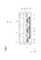
- FIG. 8 is a schematic view showing a cross section of the imaging device 1A according to the second embodiment.
- FIG. 9 is a schematic view of the imaging device 1A of FIG. 8 as viewed obliquely.
- the cover glass 500 and the sealing body 600 of FIG. 2 are omitted.
- positions on the plurality of photodiodes 101 (FIG. 8) that constitute pixels are respectively provided.
- a plurality of microlenses 401 are formed.
- the prism group 403 formed on the transparent layer 400 has a saw-like cross section like a linear Fresnel lens by forming a plurality of grooves in a straight line parallel to the X axis.
- the prism group 403 is configured of a plurality of prisms extended in the X-axis direction.
- the light beam output from the light emitting element 102 is refracted by the prism group 403 so that the light emitting element 102 illuminates the portion of the cover glass 500 on the photodiode 101 disposed next to the light emitting element 102. Be done. That is, the angles and refractive indexes of the plurality of prisms constituting the prism group 403 are adjusted to illuminate the portion of the cover glass 500 on the photodiode 101 disposed next to the light emitting element 102.
- the light reflected by the illuminated part of the object passes through the cover glass 500 and enters the imaging element 1A again.
- the light entering the imaging element 1A is received by the photodiode 101 under the microlens 401 via the microlens 401, respectively.
- a real image of an object to be imaged which contacts the upper surface of the cover glass 500 is imaged by the imaging element 1A.
- the prism group 403 bends the light emitted from the light emitting element 102 toward the photodiode 101 disposed next to the light emitting element 102.
- the light emitted from the light emitting element 102 of the light emitting unit is placed in the X axis direction (row direction) next to the light emitting element 102 of the photodiodes 101 in the light receiving unit. It can be properly guided to the finger 30 to be imaged.
- the refractive index of the transparent layer 400 may be gradually changed according to the position in the Y-axis direction of FIG. .
- the refractive index at the position of the transparent layer 400 in the Y-axis direction is adjusted to illuminate the portion of the cover glass 500 above the photodiode 101 disposed next to the light emitting element 102.
- the light emitting element 102 can appropriately illuminate the portion of the cover glass 500 above the photodiode 101 disposed next to the light emitting element 102.
- FIG. 10 is a schematic view showing a cross section of the imaging device 1B according to the third embodiment.
- the difference from the imaging device 1 according to the first embodiment is that a band-like reflection is formed by filling the space between the transparent layer 400 and the cover glass 500 with a transparent substance 450 such as a resin and extending in the X axis direction.
- the surface 451 and the semitransparent mirror 452 are formed. That is, the reflecting surface 451 and the semitransparent mirror 452 have a shape in which the direction perpendicular to the paper surface of FIG. 10 is the longitudinal direction.
- the refractive index of the transparent material 450 is set to be lower than the refractive index of the transparent layer 400.
- the light beam output from the light emitting element 102 is reflected by the reflecting surface 451 and further reflected by the semitransparent mirror 452 to illuminate a portion of the object located on the upper surface (Z-axis plus direction) of the cover glass 500.
- the light reflected by the illuminated part of the object passes through the cover glass 500 and enters the imaging element 1B again.
- the light entering the imaging element 1 B is received by the photodiode 101 under the microlens 401 through the semitransparent mirror 452 and the microlens 401.
- a real image of an object to be imaged which contacts the upper surface of the cover glass 500 is imaged by the imaging element 1B.
- the reflective surface 451 and the semitransparent mirror 452 in the imaging device 1B there is a method of insert molding a transparent substrate 450 on another thin substrate previously formed by a method such as vapor deposition or plating.
- transparent material 450 is obliquely cut to expose the surface on which reflective surface 451 and semitransparent mirror 452 are to be formed, and after reflective surface 451 and semitransparent mirror 452 are formed on the exposed surface by a method such as evaporation.
- the transparent material 450 may be bonded on the cut surface again.
- the same effects as those of the first embodiment can be obtained.
- the reflecting surface 451 and the semitransparent mirror 452 bend the light emitted from the light emitting element 102 toward the photodiode 101 disposed next to the light emitting element 102.
- the light emitted from the light emitting element 102 of the light emitting unit is placed in the X axis direction (row direction) next to the light emitting element 102 of the photodiodes 101 in the light receiving unit. It can be properly guided to the finger 30 to be imaged.
- the light emitting element 102 is disposed by one light emitting element 102 disposed between the rows in which the plurality of photodiodes 101 are arranged in the X axis direction and extending in a rectangular shape long in the X axis direction. Illuminate the portions of the cover glass 500 above the plurality of photodiodes 101 arranged in a row next to.
- the light emitting elements 102 and the rows in which the photodiodes 101 are arranged do not necessarily have to correspond one to one.
- one light emitting element 102 extended in the X-axis direction may illuminate a portion of the cover glass 500 on the plurality of photodiodes 101 arranged in a plurality of rows adjacent to the light emitting elements 102.
- Modification 2 a plurality of light emitting elements 102 extended in a rectangular shape long in the X-axis direction are disposed between the rows in which the plurality of photodiodes 101 are arranged in the X-axis direction.
- the light emitting element 102 may illuminate a portion of the cover glass 500 above the plurality of photodiodes 101 arranged in a row next to the light emitting elements 102.
- the light emitting elements 102 instead of the light emitting elements 102 extended in a rectangular shape long in the X axis direction, a plurality of light emitting elements arranged in the X axis direction may be referred to as the light emitting elements 102. That is, the light emitting element 102 is configured by arranging a plurality of light emitting elements in the X axis direction between rows in which the plurality of photodiodes 101 are arranged in the X axis direction.
- One light emitting element constituting the light emitting element 102 of the third modification and one photodiode 101 do not necessarily have to correspond one to one.
- one light emitting element constituting the light emitting element 102 may illuminate a portion of the cover glass 500 on two photodiodes 101 arranged in one row next to the light emitting element 102.
- the two light emitting elements to be configured may illuminate a portion of the cover glass 500 on one photodiode 101 arranged in a row next to the light emitting elements 102.
- one of the measures for reducing the burden of the lighting control of the light emitting element 102 by the light emitting element control circuit 107 is to increase the number of simultaneously turning on and simultaneously turning off the light emitting elements constituting the light emitting element 102. is there.
- the burden of lighting control on the light emitting element 102 can be reduced.
- a partition wall is formed between a plurality of photodiodes 101 aligned in the X axis direction and one light emitting element 102 extended in a rectangular shape long in the X axis direction. May be provided. By providing the partition wall, light leakage from the light emitting element 102 to the photodiode 101 in the substrate 100 can be prevented.
- an interference film filter for transmitting near infrared light may be provided on the transparent layer 400.
- the reason for this is to make it easier to obtain image information from near infrared light by utilizing the property that infrared light is more likely to transmit through the skin than visible light and the property that reduced hemoglobin in blood absorbs near infrared light. is there.
Landscapes
- Engineering & Computer Science (AREA)
- Multimedia (AREA)
- Signal Processing (AREA)
- Physics & Mathematics (AREA)
- General Physics & Mathematics (AREA)
- Theoretical Computer Science (AREA)
- Transforming Light Signals Into Electric Signals (AREA)
- Solid State Image Pick-Up Elements (AREA)
- Image Input (AREA)
- Facsimile Heads (AREA)
- Led Device Packages (AREA)
Abstract
撮像素子は、物体からの光を受光する受光素子が、基板上の第1方向および第1方向と交差する第2方向にそれぞれ複数配置されている受光部と、受光部の受光素子と受光素子との間で光を発する発光素子が、基板上の第2方向に複数配置されている発光部と、発光部の各発光素子の上に設けられ、発光部による光を物体へ導く導光部材と、を備える。
Description
本発明は、生体認証等に用いる撮像素子、電子機器および撮像素子の製造方法に関する。
身体の一部、例えば指や手のひらなどの指紋、掌紋、静脈パターン等を撮像し、生体認証に用いる撮像素子が知られている(特許文献1参照)。
しかしながら、従来の技術では、マイクロレンズと受光素子との間に発光層が存在するため、薄型化が難しいという問題があった。
しかしながら、従来の技術では、マイクロレンズと受光素子との間に発光層が存在するため、薄型化が難しいという問題があった。
本発明の第1の態様による撮像素子は、物体からの光を受光する受光素子が、基板上の第1方向および前記第1方向と交差する第2方向にそれぞれ複数配置されている受光部と、前記受光部の受光素子と受光素子との間で光を発する発光素子が、前記基板上の前記第2方向に複数配置されている発光部と、前記発光部の各発光素子の上に設けられ、前記発光部による光を前記物体へ導く導光部材と、を備える。
本発明の第2の態様による電子機器は、第1の態様の撮像素子を備える。
本発明の第3の態様による、上記第1の態様による撮像素子の製造方法は、基板の所定領域に前記受光素子を複数設ける工程と、前記受光素子を設けた前記基板上に配線層を形成する工程と、前記基板および前記配線層を上下反転後に、前記基板の前記受光素子の上面を露出させる工程と、前記基板の前記受光素子と前記受光素子との間に前記発光素子を設ける工程と、前記受光素子および前記発光素子を設けた前記基板上に透光部材を形成する工程と、前記透光部材にマイクロレンズおよび導光部材を形成する工程と、を含む。
本発明の第2の態様による電子機器は、第1の態様の撮像素子を備える。
本発明の第3の態様による、上記第1の態様による撮像素子の製造方法は、基板の所定領域に前記受光素子を複数設ける工程と、前記受光素子を設けた前記基板上に配線層を形成する工程と、前記基板および前記配線層を上下反転後に、前記基板の前記受光素子の上面を露出させる工程と、前記基板の前記受光素子と前記受光素子との間に前記発光素子を設ける工程と、前記受光素子および前記発光素子を設けた前記基板上に透光部材を形成する工程と、前記透光部材にマイクロレンズおよび導光部材を形成する工程と、を含む。
(第1の実施の形態)
発明の第1の実施の形態による撮像素子は、例えば現金自動預け払い機(Automated Teller Machine)、スマートフォン、ウェアラブル機器等の電子機器における生体認証用のイメージセンサとして用いられる。図1は、生体認証用の指紋を撮像する生体認証装置10を例示する図である。生体認証装置10は、上記ATMやモバイル機器等に組み込む他、上記ATMやモバイル機器等と接続して用いてもよい。
発明の第1の実施の形態による撮像素子は、例えば現金自動預け払い機(Automated Teller Machine)、スマートフォン、ウェアラブル機器等の電子機器における生体認証用のイメージセンサとして用いられる。図1は、生体認証用の指紋を撮像する生体認証装置10を例示する図である。生体認証装置10は、上記ATMやモバイル機器等に組み込む他、上記ATMやモバイル機器等と接続して用いてもよい。
図1において、生体認証装置10のセンサ窓20の位置に、後に詳述する撮像素子1(図2)のカバーグラス500が露出する。ユーザは、センサ窓20を指30で触れて指紋認証を受ける。生体認証技術は公知であるので、生体認証技術の説明については省略し、生体認証装置10に内蔵される撮像素子1の構成を中心に説明する。
なお、図1には指紋の撮像に適したサイズの生体認証装置10を例示したが、掌紋認証や静脈パターン認証等、それぞれに適したサイズの撮像素子1を備えた生体認証装置10として構成してよい。
なお、図1には指紋の撮像に適したサイズの生体認証装置10を例示したが、掌紋認証や静脈パターン認証等、それぞれに適したサイズの撮像素子1を備えた生体認証装置10として構成してよい。
<撮像素子1の構造>
図2は、生体認証装置10に内蔵される撮像素子1の断面を示す模式図である。また、図3は、図2の撮像素子1の概略構成を説明するブロック図である。図2において、互いに直交する右手座標系を構成するXYZ軸を規定し、以降のいくつかの図においては図2のXYZ軸を基準として、それぞれの図の向きがわかるように図示する。図2の場合、紙面手前方向がX軸プラス方向であり、X軸に直交する紙面右方向がY軸プラス方向であり、X軸およびY軸に直交する紙面上方向がZ軸プラス方向である。
図2は、生体認証装置10に内蔵される撮像素子1の断面を示す模式図である。また、図3は、図2の撮像素子1の概略構成を説明するブロック図である。図2において、互いに直交する右手座標系を構成するXYZ軸を規定し、以降のいくつかの図においては図2のXYZ軸を基準として、それぞれの図の向きがわかるように図示する。図2の場合、紙面手前方向がX軸プラス方向であり、X軸に直交する紙面右方向がY軸プラス方向であり、X軸およびY軸に直交する紙面上方向がZ軸プラス方向である。
撮像素子1は、いわゆる密着型の二次元イメージセンサである。撮像素子1は、例えば、単結晶シリコンの半導体基板である基板100、その裏面(Z軸マイナス方向)に形成された配線層200、基板100の表面(Z軸プラス方向)に形成された透明電極300、および透明電極300の表面(Z軸プラス方向)に形成された透明層400によって構成され、カバーグラス500と封止体600とにより気密封止されている。
基板100には、複数のフォトダイオード101と複数の発光素子102とが形成されている。複数のフォトダイオード101は、図3に示すようにX軸方向(行方向)およびY軸方向(列方向)に二次元的に配置され、撮像素子1の画素を構成している。
図3の例では、フォトダイオード101は、基板100(図2)のX軸方向(行方向)に複数個(例えば4個)が並べて離散的に配置されるとともに、上記離散的に配置されたフォトダイオード101の組が、基板100(図2)のY軸方向(列方向)に複数組(例えば4組)配置される。
また、発光素子102は、基板100のX軸方向(行方向)に長い矩形状に延設され、上記離散的に配置されたフォトダイオード101の組と、上記離散的に配置されたフォトダイオード101の別の組との間にそれぞれ配置される。
なお、撮像素子1の実際の画素数は、図示されている数よりもはるかに多い。
また、発光素子102は、基板100のX軸方向(行方向)に長い矩形状に延設され、上記離散的に配置されたフォトダイオード101の組と、上記離散的に配置されたフォトダイオード101の別の組との間にそれぞれ配置される。
なお、撮像素子1の実際の画素数は、図示されている数よりもはるかに多い。
基板100にはさらに、図3の半導体スイッチ103aおよび103b、行制御回路104、列制御回路105、および発光素子制御回路107が、同じチップ上に形成される。そして、配線層200(図2)に形成されている配線201a~配線201d等と共に、公知のCMOS(Complementary Metal Oxide Semiconductor)イメージセンサを構成している。
各発光素子102は、発光素子制御回路107に接続されている。なお、この接続は図2の配線層200に設けられた電極202および配線201c(図3)を介して行われる。発光素子102は、発光素子制御回路107によって基板100のX軸方向(行方向)ごとに点灯、消灯が制御される。
撮像素子1の各画素は、公知の4トランジスタまたは3トランジスタと称されるように、いくつかの半導体素子によって構成される。画素当たり4トランジスタの場合を簡単に説明すると、各画素は、フォトダイオード101によって生成された電荷をフローティングディフュージョンへ転送する転送トランジスタと、フォトダイオード101およびフローティングディフュージョンの電荷をリセットするためのリセットトランジスタと、電荷に基づく信号を増幅する増幅トランジスタと、増幅トランジスタの出力を対応する配線201aに接続する行選択トランジスタとを含む。図3の例では、各画素において行選択トランジスタとして機能する半導体スイッチ103aのみを図示し、他の半導体素子の図示を省略している。
なお、3トランジスタの場合は、上記4トランジスタのうちの転送トランジスタが省略される。
なお、3トランジスタの場合は、上記4トランジスタのうちの転送トランジスタが省略される。
配線201dは、出力端子108へつながる水平読み出し信号線に対応する。そして、垂直読み出し信号線に対応する各列の配線201aは、列選択トランジスタとして機能する半導体スイッチ103bを介して配線201dと接続されている。
図2の基板100の表面(Z軸プラス方向)に形成される透明電極300は、例えば、酸化インジウムスズ(ITO)によって形成されており、発光素子102の共通電極として機能する。また、配線層200には、各発光素子102に対してそれぞれ個別電極202が形成される。前述の発光素子制御回路107(図3)は、各発光素子102の発光を、対応する個別電極202を介して制御する。
透明電極300の上面(Z軸プラス方向)には、透明層400が形成されている。透明層400は、例えば透明樹脂によって形成される。本実施の形態において、透明層400の形状を加工することにより、マイクロレンズ401や斜面402を形成する。
透明層400には、各フォトダイオード101の上の位置に、それぞれマイクロレンズ401が形成される。このマイクロレンズ401は、カバーグラス500の上面(Z軸プラス方向)に位置する物体(図1の例では指30の指紋)の実像をフォトダイオード101の受光面に結像する。すなわち、マイクロレンズ401の形状や屈折率は、カバーグラス500の上面に接触している物体の接触面の実像をフォトダイオード101の受光面に結像するように調整されている。このように構成することにより、カバーグラス500に接している物体の接触面の各部位からの光が適切に集光され、対応するフォトダイオード101によってそれぞれ受光される。換言すると、各フォトダイオード101は、カバーグラス500に接している物体の、各フォトダイオード101の上(Z軸プラス方向)の部位からの光を受光する。
また、図2の発光素子102の上の透明層400には、斜面402が設けられている。発光素子102から出力された光線が斜面402で屈折することにより、発光素子102の隣に配置されているフォトダイオード101の上のカバーグラス500の部分が、発光素子102によって照明される。すなわち、斜面402の傾斜角度や屈折率は、発光素子102の隣に配置されているフォトダイオード101の上のカバーグラス500の部分を照明するように調整されている。
以上説明した撮像素子1は、上述のように、公知の方法で封止体600およびカバーグラス500によって気密封止されている。
以上説明した撮像素子1は、上述のように、公知の方法で封止体600およびカバーグラス500によって気密封止されている。
図4は、撮像素子1を斜めに見た模式図である。図4は、主として透明層400の構成を例示するものであり、図2のカバーグラス500や封止体600などは省略されている。図4によれば、基板100の上面(Z軸プラス方向)に設けられた透明層400のうち、画素を構成する複数のフォトダイオード101(図2)の上の位置に、それぞれ複数のマイクロレンズ401が形成される。また、複数のマイクロレンズ401の行と行の間に、斜面402が形成される。
斜面402は、Y軸マイナス方向に向かうほどZ軸方向の高さが低くなるように傾斜している。この斜面402により、発光素子102(図2)からの光が、発光素子102の隣に配置されているフォトダイオード101(図2)の上のカバーグラス500(図2)に向かう。すなわち、斜面402は、発光素子102(図2)から出力されZ軸プラス方向へ進む光線を、発光素子102の隣に配置されているフォトダイオード101(図2)側へ折り曲げる。
<撮像素子1の動作>
次に、撮像素子1の動作を簡単に説明する。上述したように、カバーグラス500の上面(Z軸プラス方向)に、撮像対象の物体(図1の例では指30の指紋)が接触する。カバーグラス500の物体が接触した領域が遮光されるので、撮像素子1の外部からカバーグラス500を通してフォトダイオード101の受光面に入射する光量が減少する。
次に、撮像素子1の動作を簡単に説明する。上述したように、カバーグラス500の上面(Z軸プラス方向)に、撮像対象の物体(図1の例では指30の指紋)が接触する。カバーグラス500の物体が接触した領域が遮光されるので、撮像素子1の外部からカバーグラス500を通してフォトダイオード101の受光面に入射する光量が減少する。
撮像素子1は、例えば、複数のフォトダイオード101で受光された光量が予め定めた値より低くなった場合に、撮像動作を開始するように構成される。撮像動作を開始すると、先ず発光素子制御回路107(図3)が、複数の発光素子102を順次発光させる。各発光素子102が発した光は、各発光素子102の上の斜面402(図2)によって屈折され、各発光素子102の隣の行に配置された複数のフォトダイオード101の上のカバーグラス500の上面(Z軸プラス方向)に位置する物体の部分を照明する。
物体の照明された部位で反射された光は、カバーグラス500を透過して再び撮像素子1に進入する。撮像素子1に進入した光は、マイクロレンズ401を介してマイクロレンズ401の下のフォトダイオード101でそれぞれ受光される。このようにして、カバーグラス500の上面に接触する撮像対象の物体の等倍の実像が、撮像素子1によって撮像される。
<撮像タイミング動作>
図5は、撮像素子1による撮像動作のタイミングを説明する図である。撮像素子1はCMOSイメージセンサであるため、画素を構成するフォトダイオード101の行(図3におけるX軸方向の並び)ごとに、露光動作と読み出し動作とを行う。
図5は、撮像素子1による撮像動作のタイミングを説明する図である。撮像素子1はCMOSイメージセンサであるため、画素を構成するフォトダイオード101の行(図3におけるX軸方向の並び)ごとに、露光動作と読み出し動作とを行う。
図5のタイミングチャートは、n行目およびn+1行目のフォトダイオード101と、n行およびn+1行に対応する発光素子102の動作を示している。まず、行制御回路104(図3)が、配線201bを介してn行目に対する行選択パルスを行選択トランジスタ(半導体スイッチ103a)へ供給して行選択トランジスタ(半導体スイッチ103a)をオンさせる。そして、時刻t0nにおいて、行制御回路104(図3)が、配線201bを介してn行目の各フォトダイオード101に対するリセットパルスRSTnを不図示のリセットトランジスタへ供給する。これにより、リセットトランジスタがオンしてn行目の各フォトダイオード101および対応するフローティングディフュージョンに蓄積されている電荷がリセットされる。
同時に、時刻t0nにおいて、発光素子制御回路107(図3)が、配線201cを介してn行目の発光素子102に対する発光素子制御信号ILLnをHレベルにする。これによってn行目の発光素子102が点灯する。その結果、n行目の発光素子102からの照明光が前述の透明層400(図2)の斜面402で屈折され、n行目のフォトダイオード101の上のカバーグラス500上の物体の部分を照明する。物体の照明された部位で反射された光は、マイクロレンズ401を介してフォトダイオード101に入射する。
次に、時刻t1nにおいて、行制御回路104(図3)が、配線201bを介してn行目の画素に対する転送パルスTRnを不図示の転送トランジスタに供給する。これにより、入射した光によって各フォトダイオード101で生成された電荷が、対応するフローティングディフュージョンに転送される。
同時に、時刻t1nにおいて、発光素子制御回路107が、配線201cを介してn行目の発光素子102に対する発光素子制御信号ILLnをLレベルにする。これによってn行目の発光素子102が消灯する。n行目の発光素子102が点灯している時刻t0nから時刻t1nまでの時間Tnが、n行目のフォトダイオード101の露光時間となる。すなわち、n行目のフォトダイオード101の露光時間の制御をn行目の発光素子102の点灯時間の制御によって行うことができる。
n行目のフォトダイオード101から電荷の転送が終了すると、時刻t2nにおいて、列制御回路105(図3)が、各列の半導体スイッチ103b(列選択トランジスタ)へ読み出しパルスROnを順次供給する。これにより、n行目のフローティングディフュージョンに転送された電荷に基づく増幅信号が、半導体スイッチ103bによって選択された列の配線201aおよび配線201dを介して順次出力端子108から読み出される。以上により、n行目の画素を構成する複数のフォトダイオード101における露光動作と読み出し動作が終了する。
n行目と同様にして、n+1行目についても露光動作と読み出し動作とを行う。以下同様のことを繰り返し、撮像素子1の全ての行について露光動作と読み出し動作とを行うことによって、物体の画像情報が得られる。
なお、CMOSイメージセンサの特性として、1行分の読み出しが終わらないと次の行の読み出しを開始することができない。したがって、n+1行目に対する行選択パルスの供給、リセットパルスRSTn+1の供給、転送パルスTRn+1の供給、および発光素子102に対する発光素子制御信号ILLn+1の制御タイミングも、読み出しパルスROnによる読み出し時間だけ後ろにシフトしたものになる。その後の読み出しも順次シフトして行う、いわゆるローリング読み出しである。
なお、露光時間Tn+1は基本的にはTnと同じでよいが、発光素子102の特性のばらつきなどを考慮して、行ごとに変えてもよい。
<製造方法>
図6および図7を参照して、撮像素子1の製造手順の一例を説明する。図6(a)において、例えばシリコン基板100の所定の位置に、各画素を形成するフォトダイオード101、フローティングディフュージョン、およびトランジスタ等の周辺の素子を、公知の手法を用いて形成する。
なお、図6および図7においては、フローティングディフュージョンやトランジスタ等の図示を省略するものとする。
図6および図7を参照して、撮像素子1の製造手順の一例を説明する。図6(a)において、例えばシリコン基板100の所定の位置に、各画素を形成するフォトダイオード101、フローティングディフュージョン、およびトランジスタ等の周辺の素子を、公知の手法を用いて形成する。
なお、図6および図7においては、フローティングディフュージョンやトランジスタ等の図示を省略するものとする。
図6(b)において、シリコン基板100上に配線層200を公知の手法を用いて形成する。配線層200には、撮像素子1を駆動する制御信号や、撮像素子1で生成された信号を入出力するための配線201a、201b、201c、201dを多層に形成する。このとき、後述する発光素子102用の電極202を、配線層200の最下層に形成しておく。
なお、図6および図7においては、配線201c、201dの図示を省略している。
なお、図6および図7においては、配線201c、201dの図示を省略している。
図6(c)において、シリコン基板100の上下を反転する。上限反転したことによって上記電極202が配線層200の上層に位置する。図6(d)において、シリコン基板100の上面より、フォトダイオード101の受光面が表面に現れるまでシリコン基板100を、例えばケミカルエッチングなどの方法で削り込む。
図7(a)において、発光素子102用の電極202に対応するシリコン基板100の領域を、例えばフォトリソグラフィなどの手法を用いることによって選択的に除去し、発光電極202を露出する。
図7(b)において、シリコン基板100を除去した領域に発光素子102を形成する。予め電極202を設けてあるので、後工程を簡単にすることができる。発光素子102は、例えば化合物半導体を用いた発光ダイオード(LED)あるいは有機EL(エレクトロルミネッセンス)などである。発光素子102を形成する方法としては、フォトリソグラフィを利用した結晶成長、蒸着、スパッタリング、印刷等を適宜用いることができる。
図7(b)によれば、フォトダイオード101と発光素子102とを略同じ平面上に形成できるので、例えばフォトダイオード101に対して発光層を積層する場合と比べて、撮像素子1を薄型に構成することができる。
次に図7(c)に示すように、シリコン基板100および発光素子102の上に透明電極300を形成する。透明電極300は、前述のように酸化インジウムスズ(ITO)等を用いる。上述した通り、本実施の形態では透明電極300を発光素子102の共通電極として用いる。
そして、図7(d)に示すように、透明電極300の上に透明層400を形成する。さらに、透明層400には、画素を構成する複数のフォトダイオード101の上に、それぞれマイクロレンズ401を形成する。また、発光素子102の上に、斜面402を形成する。これらマイクロレンズ401や斜面402の形成方法は、透明層400を形成した後に型押しにより成形する方法でもよいし、予め注型重合などで成形した透明層400を透明電極300の上面に接着する方法でもよい。
以上説明した第1の実施の形態によれば、次の作用効果が得られる。
(1)撮像素子1は、撮像対象とする物体(上記例では指30)からの光を受光するフォトダイオード101が、基板100上のX軸方向(行方向)およびY軸方向(列方向)にそれぞれ複数配置されている受光部(複数のフォトダイオード101の総称)と、受光部のフォトダイオード101とフォトダイオード101との間で光を発する発光素子102が、基板100上のY軸方向(列方向)に複数配置されている発光部(複数の発光素子102の総称)と、発光部の各発光素子102の上に設けられ、発光部による光を物体へ導く斜面402とを備える。
同じ基板100上に受光部と発光部を配置したことで、受光部と発光部とを積層させる場合よりも撮像素子1を薄型に構成することができる。また、発光部の発光素子102が発した光を斜面402により指30へ導いたので、指30を適切に照明し、指30で反射された光を受光部のフォトダイオード101によって受光することができる。このように構成したことによって、撮像素子1は、指30(指紋)の像を適切に撮像することができる。
(1)撮像素子1は、撮像対象とする物体(上記例では指30)からの光を受光するフォトダイオード101が、基板100上のX軸方向(行方向)およびY軸方向(列方向)にそれぞれ複数配置されている受光部(複数のフォトダイオード101の総称)と、受光部のフォトダイオード101とフォトダイオード101との間で光を発する発光素子102が、基板100上のY軸方向(列方向)に複数配置されている発光部(複数の発光素子102の総称)と、発光部の各発光素子102の上に設けられ、発光部による光を物体へ導く斜面402とを備える。
同じ基板100上に受光部と発光部を配置したことで、受光部と発光部とを積層させる場合よりも撮像素子1を薄型に構成することができる。また、発光部の発光素子102が発した光を斜面402により指30へ導いたので、指30を適切に照明し、指30で反射された光を受光部のフォトダイオード101によって受光することができる。このように構成したことによって、撮像素子1は、指30(指紋)の像を適切に撮像することができる。
(2)上記(1)の撮像素子1において、発光部の各発光素子102は、基板100上のX軸方向(行方向)に長い矩形状に延設され、受光部のX軸方向(行方向)に配置されている複数のフォトダイオード101と、発光部の発光素子102とを、基板100上のY軸方向(列方向)に交互に配置した。
発光部の発光素子102を基板100上のX軸方向(行方向)に長い矩形状に構成したので、発光部を行ごとに分けて点灯、消灯を制御することができる。このように構成したことによって、例えば、受光部のX軸方向(行方向)に配置されている複数のフォトダイオード101で撮像するタイミングに合わせて、発光素子102を順番に点灯させることができる。
発光部の発光素子102を基板100上のX軸方向(行方向)に長い矩形状に構成したので、発光部を行ごとに分けて点灯、消灯を制御することができる。このように構成したことによって、例えば、受光部のX軸方向(行方向)に配置されている複数のフォトダイオード101で撮像するタイミングに合わせて、発光素子102を順番に点灯させることができる。
(3)上記(1)または(2)に記載の撮像素子1において、斜面402は、発光素子102が発した光を発光素子102の隣に配置されているフォトダイオード101側へ折り曲げる。このように構成したので、発光部の発光素子102が発した光を、受光部のフォトダイオード101のうちの発光素子102の隣にX軸方向(行方向)に配置されているフォトダイオード101が撮像する指30へと適切に導くことができる。
(4)上記(1)から(3)の撮像素子1において、受光部の各フォトダイオード101は、指30の異なる部位で反射された光を受光するので、撮像素子1は、指30(指紋)の像を適切に撮像することができる。
(5)上記(4)の撮像素子1において、受光部の各フォトダイオード101に設けられ、物体の反射光をフォトダイオード101に集光するマイクロレンズ401を備えるので、マイクロレンズ401を設けない場合に比べて、明るく高品位に撮像することができる。
(6)上記(5)の撮像素子1において、受光部および発光部の上面に透明層400を備え、斜面402およびマイクロレンズ401は、透明層400に形成した。斜面402およびマイクロレンズ401を異なる材質で形成する場合に比べて製造が容易になり、製造コストを低減することができる。
(7)上記(6)の撮像素子1において、受光部は、透明層400より物体側に設けられるカバーガラス500に接している物体の等倍像を撮像する。このように構成したので、指紋等の生体認証に適した撮像素子1を得ることができる。
(8)撮像素子1の製造方法は、基板100の所定領域にフォトダイオード101を複数設ける工程と、フォトダイオード101を設けた基板100上に配線層200を形成する工程と、基板100および配線層200を上下反転後に、基板100のフォトダイオード101の上面を露出させるエッチング工程と、基板100のフォトダイオード101とフォトダイオード101との間に発光素子102を設ける工程と、フォトダイオード101および発光素子102を設けた基板100上に透光部材400を形成する工程と、透光部材400にマイクロレンズ401および斜面402を形成する工程と、を含む。
このように構成したので、同じ基板100上に受光部と発光部を配置できるため、受光部と発光部とを積層させる場合よりも薄型の撮像素子1を製造することができる。
このように構成したので、同じ基板100上に受光部と発光部を配置できるため、受光部と発光部とを積層させる場合よりも薄型の撮像素子1を製造することができる。
(9)上記(8)の製造方法において、配線層200を形成する工程は、基板100のフォトダイオード101とフォトダイオード101との間にそれぞれ電極202を最下層に含む配線層200を基板100上に形成し、発光素子102を設ける工程は、基板100の電極202の上にそれぞれ発光素子102を設ける。このように構成したので、後から電極202を設ける場合に比べて、製造が容易になり、製造コストを低減することができる。
(第2の実施の形態)
第1の実施の形態による撮像素子1の透明層400に形成された斜面402に代えて、ストライプ状の複数のプリズムで構成されるプリズム群403を透明層400に形成してもよい。図8は、第2の実施の形態による撮像素子1Aの断面を示す模式図である。
第1の実施の形態による撮像素子1の透明層400に形成された斜面402に代えて、ストライプ状の複数のプリズムで構成されるプリズム群403を透明層400に形成してもよい。図8は、第2の実施の形態による撮像素子1Aの断面を示す模式図である。
図9は、図8の撮像素子1Aを斜めに見た模式図である。図9において、図2のカバーグラス500や封止体600などは省略されている。また、図4の場合と同様に、基板100の上面(Z軸プラス方向)に設けられた透明層400のうち、画素を構成する複数のフォトダイオード101(図8)の上の位置に、それぞれ複数のマイクロレンズ401が形成されている。
透明層400に形成されたプリズム群403は、X軸と平行な直線状に複数の溝が形成されることにより、リニアフレネルレンズのようなのこぎり状の断面を有する。換言すると、プリズム群403は、X軸方向に長く延設した複数のプリズムによって構成される。
図8において、発光素子102から出力された光線がプリズム群403で屈折することにより、発光素子102の隣に配置されているフォトダイオード101の上のカバーグラス500の部分が、発光素子102によって照明される。すなわち、プリズム群403を構成する複数のプリズムの角度や屈折率は、発光素子102の隣に配置されているフォトダイオード101の上のカバーグラス500の部分を照明するように調整されている。
物体の照明された部位で反射された光は、カバーグラス500を透過して再び撮像素子1Aに進入する。撮像素子1Aに進入した光は、マイクロレンズ401を介してマイクロレンズ401の下のフォトダイオード101でそれぞれ受光される。このようにして、カバーグラス500の上面に接触する撮像対象の物体の実像が、撮像素子1Aによって撮像される。
第2の実施の形態によれば、第1の実施の形態と同様の作用効果が得られる。
とくに、撮像素子1Aにおいて、プリズム群403は、発光素子102が発した光を発光素子102の隣に配置されているフォトダイオード101側へ折り曲げる。このように構成したので、発光部の発光素子102が発した光を、受光部のフォトダイオード101のうちの発光素子102の隣にX軸方向(行方向)に配置されているフォトダイオード101が撮像する指30へと適切に導くことができる。
とくに、撮像素子1Aにおいて、プリズム群403は、発光素子102が発した光を発光素子102の隣に配置されているフォトダイオード101側へ折り曲げる。このように構成したので、発光部の発光素子102が発した光を、受光部のフォトダイオード101のうちの発光素子102の隣にX軸方向(行方向)に配置されているフォトダイオード101が撮像する指30へと適切に導くことができる。
なお、第2の実施の形態の変形例として、プリズム群403を設ける代わりに、透明層400の屈折率を図2のY軸方向の位置に応じて徐々に変化させるように構成してもよい。透明層400の屈折率をY軸方向の位置に応じて徐々に変化させることによって、発光素子102から出力された光線が、透明層400で屈折する。透明層400のY軸方向の位置における屈折率は、発光素子102の隣に配置されているフォトダイオード101の上のカバーグラス500の部分を照明するように調整される。
このように構成することによっても、発光素子102の隣に配置されているフォトダイオード101の上のカバーグラス500の部分を、発光素子102によって適切に照明することができる。
このように構成することによっても、発光素子102の隣に配置されているフォトダイオード101の上のカバーグラス500の部分を、発光素子102によって適切に照明することができる。
(第3の実施の形態)
図10は、第3の実施の形態による撮像素子1Bの断面を示す模式図である。第1の実施の形態による撮像素子1と相違する点は、透明層400とカバーグラス500との間を樹脂等の透明物質450で充填し、そこにX軸方向に長く延設した帯状の反射面451および半透鏡面452を形成したことである。すなわち、反射面451および半透鏡面452は、図10の紙面に垂直な方向を長手方向とする形状を有している。
図10は、第3の実施の形態による撮像素子1Bの断面を示す模式図である。第1の実施の形態による撮像素子1と相違する点は、透明層400とカバーグラス500との間を樹脂等の透明物質450で充填し、そこにX軸方向に長く延設した帯状の反射面451および半透鏡面452を形成したことである。すなわち、反射面451および半透鏡面452は、図10の紙面に垂直な方向を長手方向とする形状を有している。
図10において、透明物質450の屈折率は、透明層400の屈折率より低く設定される。発光素子102から出力された光線は、反射面451で反射され、さらに半透鏡面452で反射されてカバーグラス500の上面(Z軸プラス方向)に位置する物体の部分を照明する。
物体の照明された部位で反射された光は、カバーグラス500を透過して再び撮像素子1Bに進入する。撮像素子1Bに進入した光は、半透鏡452およびマイクロレンズ401を介してマイクロレンズ401の下のフォトダイオード101でそれぞれ受光される。このようにして、カバーグラス500の上面に接触する撮像対象の物体の実像が、撮像素子1Bによって撮像される。
撮像素子1Bにおける反射面451および半透鏡面452の形成方法としては、例えば、予め別の薄い基板に蒸着やメッキ等の方法で形成されたものを、透明物質450にインサートモールドする方法がある。
あるいは、透明物質450を斜めにカットして反射面451および半透鏡面452を形成すべき面を露出させ、露出された面に蒸着などの方法で反射面451および半透鏡面452を形成した後に、再び透明物質450をカットした面で接着するようにしてもよい。
以上説明したように、第3の実施の形態によれば、第1の実施の形態と同様の作用効果が得られる。
とくに、撮像素子1Bにおいて、反射面451および半透鏡面452は、発光素子102が発した光を発光素子102の隣に配置されているフォトダイオード101側へ折り曲げる。このように構成したので、発光部の発光素子102が発した光を、受光部のフォトダイオード101のうちの発光素子102の隣にX軸方向(行方向)に配置されているフォトダイオード101が撮像する指30へと適切に導くことができる。
とくに、撮像素子1Bにおいて、反射面451および半透鏡面452は、発光素子102が発した光を発光素子102の隣に配置されているフォトダイオード101側へ折り曲げる。このように構成したので、発光部の発光素子102が発した光を、受光部のフォトダイオード101のうちの発光素子102の隣にX軸方向(行方向)に配置されているフォトダイオード101が撮像する指30へと適切に導くことができる。
次のような変形も本発明の範囲内であり、変形例の一つ、もしくは複数を上述の実施形態と組み合わせることも可能である。
(変形例1)
上述した各実施の形態では、X軸方向に複数のフォトダイオード101が並ぶ行と行の間に配置され、X軸方向に長い矩形状に延設された一つの発光素子102によって、発光素子102の隣の1行に配置された複数のフォトダイオード101の上のカバーグラス500の部分を照明した。発光素子102と、フォトダイオード101が並ぶ行とは、必ずしも1対1に対応させなくてもよい。例えば、X軸方向に延設された一つの発光素子102によって、発光素子102の隣の複数行に配置された複数のフォトダイオード101の上のカバーグラス500の部分を照明してもよい。
(変形例1)
上述した各実施の形態では、X軸方向に複数のフォトダイオード101が並ぶ行と行の間に配置され、X軸方向に長い矩形状に延設された一つの発光素子102によって、発光素子102の隣の1行に配置された複数のフォトダイオード101の上のカバーグラス500の部分を照明した。発光素子102と、フォトダイオード101が並ぶ行とは、必ずしも1対1に対応させなくてもよい。例えば、X軸方向に延設された一つの発光素子102によって、発光素子102の隣の複数行に配置された複数のフォトダイオード101の上のカバーグラス500の部分を照明してもよい。
(変形例2)
また、変形例1とは反対に、X軸方向に複数のフォトダイオード101が並ぶ行と行との間に、X軸方向に長い矩形状に延設された発光素子102を複数配置し、複数の発光素子102によって、これら発光素子102の隣の1行に配置された複数のフォトダイオード101の上のカバーグラス500の部分を照明してもよい。
また、変形例1とは反対に、X軸方向に複数のフォトダイオード101が並ぶ行と行との間に、X軸方向に長い矩形状に延設された発光素子102を複数配置し、複数の発光素子102によって、これら発光素子102の隣の1行に配置された複数のフォトダイオード101の上のカバーグラス500の部分を照明してもよい。
(変形例3)
さらにまた、X軸方向に長い矩形状に延設された発光素子102に代えて、X軸方向に並べた複数の発光素子を、発光素子102と称してもよい。すなわち、X軸方向に複数のフォトダイオード101が並ぶ行と行の間に、X軸方向に複数の発光素子を並べて、発光素子102を構成する。
さらにまた、X軸方向に長い矩形状に延設された発光素子102に代えて、X軸方向に並べた複数の発光素子を、発光素子102と称してもよい。すなわち、X軸方向に複数のフォトダイオード101が並ぶ行と行の間に、X軸方向に複数の発光素子を並べて、発光素子102を構成する。
変形例3の発光素子102を構成する一つの発光素子と、一つのフォトダイオード101とは、必ずしも1対1に対応させなくてもよい。例えば、発光素子102を構成する一つの発光素子で、発光素子102の隣の1行に配置された二つのフォトダイオード101の上のカバーグラス500の部分を照明してもよく、発光素子102を構成する二つの発光素子で、発光素子102の隣の1行に配置された一つのフォトダイオード101の上のカバーグラス500の部分を照明してもよい。
なお、発光素子制御回路107による発光素子102の点灯制御の負担を軽減するための方策の一つは、発光素子102を構成する発光素子の中で同時に点灯し、同時に消灯する数を増やすことである。極端な例では、撮像素子1に設けられる全ての発光素子102を同時に点灯し、全ての発光素子102を同時に消灯すると、発光素子102を異なるタイミングで個別に点灯し、消灯する場合と比べて、発光素子102に対する点灯制御の負担を軽減することができる。
(変形例4)
上述した撮像素子1(1A、1B)の基板100において、X軸方向に並んだ複数のフォトダイオード101と、X軸方向に長い矩形状に延設された一つの発光素子102との間に隔壁を設けてもよい。隔壁を設けることにより、基板100における発光素子102からフォトダイオード101への漏光を防止することができる。
上述した撮像素子1(1A、1B)の基板100において、X軸方向に並んだ複数のフォトダイオード101と、X軸方向に長い矩形状に延設された一つの発光素子102との間に隔壁を設けてもよい。隔壁を設けることにより、基板100における発光素子102からフォトダイオード101への漏光を防止することができる。
(変形例5)
なお、生体認証装置10によって静脈パターンを撮像する場合は、近赤外光を透過させるための干渉膜フィルタを透明層400に設けるとよい。この理由は、赤外線が可視光より皮膚を透過しやすい性質と、血液中の還元ヘモグロビンが近赤外光を吸収する性質とを利用して、近赤外光による画像情報を得やすくするためである。
なお、生体認証装置10によって静脈パターンを撮像する場合は、近赤外光を透過させるための干渉膜フィルタを透明層400に設けるとよい。この理由は、赤外線が可視光より皮膚を透過しやすい性質と、血液中の還元ヘモグロビンが近赤外光を吸収する性質とを利用して、近赤外光による画像情報を得やすくするためである。
(変形例6)
以上の説明では、撮像素子1を生体認証装置10に用いる例を説明したが、撮像素子1を、QRコード(登録商標)を撮像する装置に用いてもよい。また、撮像素子1を、例えば紙幣の真偽判定用として紙幣の一部を撮像するスキャナ装置に用いてもよい。
以上の説明では、撮像素子1を生体認証装置10に用いる例を説明したが、撮像素子1を、QRコード(登録商標)を撮像する装置に用いてもよい。また、撮像素子1を、例えば紙幣の真偽判定用として紙幣の一部を撮像するスキャナ装置に用いてもよい。
上記では、種々の実施の形態および変形例を説明したが、本発明はこれらの内容に限定されるものではない。本発明の技術的思想の範囲内で考えられるその他の態様も本発明の範囲内に含まれる。
次の優先権基礎出願の開示内容は引用文としてここに組み込まれる。
日本国特許出願2017年第138051号(2017年7月14日出願)
日本国特許出願2017年第138051号(2017年7月14日出願)
1、1A、1B…撮像素子
30…指(物体)
100…基板
101…フォトダイオード
102…発光素子
200…配線層
202…電極
300…透明電極
400…透明層
401…マイクロレンズ
402…斜面
403…プリズム群
500…カバーガラス
30…指(物体)
100…基板
101…フォトダイオード
102…発光素子
200…配線層
202…電極
300…透明電極
400…透明層
401…マイクロレンズ
402…斜面
403…プリズム群
500…カバーガラス
Claims (12)
- 物体からの光を受光する受光素子が、基板上の第1方向および前記第1方向と交差する第2方向にそれぞれ複数配置されている受光部と、
前記受光部の受光素子と受光素子との間で光を発する発光素子が、前記基板上の前記第2方向に複数配置されている発光部と、
前記発光部の各発光素子の上に設けられ、前記発光部による光を前記物体へ導く導光部材と、
を備える撮像素子。 - 請求項1に記載の撮像素子において、
前記発光部の各発光素子は、前記基板上の前記第1方向に延設され、
前記受光部の前記第1方向に配置されている複数の受光素子と、前記発光部の発光素子とが、前記基板上の前記第2方向に交互に配置される撮像素子。 - 請求項1または請求項2に記載の撮像素子において、
前記導光部材は、前記発光素子が発した光を隣に配置されている前記受光素子側へ折り曲げる撮像素子。 - 請求項1から請求項3までのいずれか一項に記載の撮像素子において、
前記受光部の各受光素子は、前記物体の異なる部位で反射された光を受光する撮像素子。 - 請求項4に記載の撮像素子において、
前記受光部の各受光素子に設けられ、前記物体の反射光を前記受光素子に集光するマイクロレンズを備える撮像素子。 - 請求項5に記載の撮像素子において、
前記受光部および前記発光部の上面に透明層を備え、
前記導光部材および前記マイクロレンズは、前記透明層に形成される撮像素子。 - 請求項6に記載の撮像素子において、
前記受光部は、前記透明層より前記物体側に設けられるカバーガラスに接している前記物体の等倍像を撮像する撮像素子。 - 物体へ光を照射する発光素子が基板の第1ライン上に設けられたライン状の発光部と、
前記物体からの光を受光する受光素子が前記基板の前記第1ラインとは異なる第2ライン上に離散的に設けられた複数の受光部と、
前記発光素子の上に設けられ、前記発光部による光を前記物体へ導く導光部材と、
を備える撮像素子。 - 前記複数の受光部上にそれぞれに設けられ、前記物体からの光を前記受光素子に集光させる複数の集光部を備えた請求項8に記載の撮像素子。
- 請求項1から請求項9までのいずれか一項に記載の撮像素子を備える電子機器。
- 請求項1から請求項9までのいずれか一項に記載の撮像素子の製造方法において、
基板の所定領域に前記受光素子を複数設ける工程と、
前記受光素子を設けた前記基板上に配線層を形成する工程と、
前記基板および前記配線層を上下反転後に、前記基板の前記受光素子の上面を露出させる工程と、
前記基板の前記受光素子と前記受光素子との間に前記発光素子を設ける工程と、
前記受光素子および前記発光素子を設けた前記基板上に透光部材を形成する工程と、
前記透光部材にマイクロレンズおよび導光部材を形成する工程と、
を含む撮像素子の製造方法。 - 請求項11に記載の撮像素子の製造方法において、
前記配線層を形成する工程は、前記基板の前記受光素子と前記受光素子との間にそれぞれ電極を最下層に含む配線層を、前記配線層として前記基板上に形成し、
前記発光素子を設ける工程は、前記基板の前記電極の上にそれぞれ前記発光素子を設ける撮像素子の製造方法。
Applications Claiming Priority (2)
| Application Number | Priority Date | Filing Date | Title |
|---|---|---|---|
| JP2017-138051 | 2017-07-14 | ||
| JP2017138051A JP2020155426A (ja) | 2017-07-14 | 2017-07-14 | 撮像素子、電子機器および撮像素子の製造方法 |
Publications (1)
| Publication Number | Publication Date |
|---|---|
| WO2019013166A1 true WO2019013166A1 (ja) | 2019-01-17 |
Family
ID=65002598
Family Applications (1)
| Application Number | Title | Priority Date | Filing Date |
|---|---|---|---|
| PCT/JP2018/025890 Ceased WO2019013166A1 (ja) | 2017-07-14 | 2018-07-09 | 撮像素子、電子機器および撮像素子の製造方法 |
Country Status (2)
| Country | Link |
|---|---|
| JP (1) | JP2020155426A (ja) |
| WO (1) | WO2019013166A1 (ja) |
Cited By (2)
| Publication number | Priority date | Publication date | Assignee | Title |
|---|---|---|---|---|
| JPWO2020004056A1 (ja) * | 2018-06-28 | 2020-07-09 | Dic株式会社 | 粘着テープ及び物品 |
| US11105745B2 (en) | 2019-10-10 | 2021-08-31 | Visera Technologies Company Limited | Biosensor |
Citations (5)
| Publication number | Priority date | Publication date | Assignee | Title |
|---|---|---|---|---|
| JP2004134514A (ja) * | 2002-10-09 | 2004-04-30 | Canon Inc | 裏面入射型撮像センサ |
| JP2005110896A (ja) * | 2003-10-07 | 2005-04-28 | Canon Inc | 指センサ |
| JP2009003821A (ja) * | 2007-06-25 | 2009-01-08 | Hitachi Ltd | 撮像装置及びこれを搭載した装置 |
| JP2012221083A (ja) * | 2011-04-06 | 2012-11-12 | Seiko Epson Corp | センシング装置および電子機器 |
| JP2017107309A (ja) * | 2015-12-08 | 2017-06-15 | 株式会社日立製作所 | 指静脈認証装置 |
-
2017
- 2017-07-14 JP JP2017138051A patent/JP2020155426A/ja active Pending
-
2018
- 2018-07-09 WO PCT/JP2018/025890 patent/WO2019013166A1/ja not_active Ceased
Patent Citations (5)
| Publication number | Priority date | Publication date | Assignee | Title |
|---|---|---|---|---|
| JP2004134514A (ja) * | 2002-10-09 | 2004-04-30 | Canon Inc | 裏面入射型撮像センサ |
| JP2005110896A (ja) * | 2003-10-07 | 2005-04-28 | Canon Inc | 指センサ |
| JP2009003821A (ja) * | 2007-06-25 | 2009-01-08 | Hitachi Ltd | 撮像装置及びこれを搭載した装置 |
| JP2012221083A (ja) * | 2011-04-06 | 2012-11-12 | Seiko Epson Corp | センシング装置および電子機器 |
| JP2017107309A (ja) * | 2015-12-08 | 2017-06-15 | 株式会社日立製作所 | 指静脈認証装置 |
Cited By (3)
| Publication number | Priority date | Publication date | Assignee | Title |
|---|---|---|---|---|
| JPWO2020004056A1 (ja) * | 2018-06-28 | 2020-07-09 | Dic株式会社 | 粘着テープ及び物品 |
| US11105745B2 (en) | 2019-10-10 | 2021-08-31 | Visera Technologies Company Limited | Biosensor |
| TWI796556B (zh) * | 2019-10-10 | 2023-03-21 | 采鈺科技股份有限公司 | 生物感測器 |
Also Published As
| Publication number | Publication date |
|---|---|
| JP2020155426A (ja) | 2020-09-24 |
Similar Documents
| Publication | Publication Date | Title |
|---|---|---|
| CN110047872B (zh) | 显示装置 | |
| CN108629269B (zh) | 光学成像设备 | |
| CN108734073B (zh) | 一种检测装置及终端设备 | |
| US20210342566A1 (en) | Under-display-type fingerprint authentication sensor module and under-display-type fingerprint authentication device | |
| US7408135B2 (en) | Imaging device having dual opening with open/close unit and electronic equipment incorporated therein the same | |
| CN110062931A (zh) | 指纹识别装置、指纹识别方法和电子设备 | |
| US8306287B2 (en) | Biometrics authentication system | |
| TWI387902B (zh) | 光學導向裝置及光學導向方法 | |
| US20200184246A1 (en) | Optical fingerprint sensing module | |
| JP2010539562A (ja) | 光ナビゲーションデバイス | |
| CN113206208B (zh) | 显示面板及显示设备 | |
| CN101447018A (zh) | 摄像设备及其方法 | |
| US20170221960A1 (en) | Contact image sensor | |
| JP7780273B2 (ja) | 表示装置、光電変換装置、電子機器、照明装置、移動体、および、ウェアラブルデバイス | |
| US11068684B2 (en) | Fingerprint authentication sensor module and fingerprint authentication device | |
| KR20180135584A (ko) | 지문인식 기능을 구비한 디스플레이 | |
| CN111133442B (zh) | 指纹检测的装置和电子设备 | |
| WO2019013166A1 (ja) | 撮像素子、電子機器および撮像素子の製造方法 | |
| US11881047B2 (en) | Optical sensor | |
| KR102886418B1 (ko) | 화상 표시 장치 및 전자 기기 | |
| US11848306B2 (en) | Tiled image sensor | |
| JP5687564B2 (ja) | 撮像システムおよび撮像システム用の固体撮像装置の製造方法 | |
| US11942489B2 (en) | Image reading device | |
| TW202026832A (zh) | 指紋辨識裝置 | |
| TWI886905B (zh) | 顯示裝置 |
Legal Events
| Date | Code | Title | Description |
|---|---|---|---|
| 121 | Ep: the epo has been informed by wipo that ep was designated in this application |
Ref document number: 18831552 Country of ref document: EP Kind code of ref document: A1 |
|
| NENP | Non-entry into the national phase |
Ref country code: DE |
|
| 122 | Ep: pct application non-entry in european phase |
Ref document number: 18831552 Country of ref document: EP Kind code of ref document: A1 |
|
| NENP | Non-entry into the national phase |
Ref country code: JP |