WO2018235847A1 - Liquid crystal panel - Google Patents
Liquid crystal panel Download PDFInfo
- Publication number
- WO2018235847A1 WO2018235847A1 PCT/JP2018/023385 JP2018023385W WO2018235847A1 WO 2018235847 A1 WO2018235847 A1 WO 2018235847A1 JP 2018023385 W JP2018023385 W JP 2018023385W WO 2018235847 A1 WO2018235847 A1 WO 2018235847A1
- Authority
- WO
- WIPO (PCT)
- Prior art keywords
- liquid crystal
- polarizing plate
- reflection
- crystal panel
- state
- Prior art date
Links
Images


Classifications
-
- G—PHYSICS
- G02—OPTICS
- G02F—OPTICAL DEVICES OR ARRANGEMENTS FOR THE CONTROL OF LIGHT BY MODIFICATION OF THE OPTICAL PROPERTIES OF THE MEDIA OF THE ELEMENTS INVOLVED THEREIN; NON-LINEAR OPTICS; FREQUENCY-CHANGING OF LIGHT; OPTICAL LOGIC ELEMENTS; OPTICAL ANALOGUE/DIGITAL CONVERTERS
- G02F1/00—Devices or arrangements for the control of the intensity, colour, phase, polarisation or direction of light arriving from an independent light source, e.g. switching, gating or modulating; Non-linear optics
- G02F1/01—Devices or arrangements for the control of the intensity, colour, phase, polarisation or direction of light arriving from an independent light source, e.g. switching, gating or modulating; Non-linear optics for the control of the intensity, phase, polarisation or colour
- G02F1/13—Devices or arrangements for the control of the intensity, colour, phase, polarisation or direction of light arriving from an independent light source, e.g. switching, gating or modulating; Non-linear optics for the control of the intensity, phase, polarisation or colour based on liquid crystals, e.g. single liquid crystal display cells
- G02F1/133—Constructional arrangements; Operation of liquid crystal cells; Circuit arrangements
- G02F1/1333—Constructional arrangements; Manufacturing methods
- G02F1/1335—Structural association of cells with optical devices, e.g. polarisers or reflectors
- G02F1/133553—Reflecting elements
-
- G—PHYSICS
- G02—OPTICS
- G02F—OPTICAL DEVICES OR ARRANGEMENTS FOR THE CONTROL OF LIGHT BY MODIFICATION OF THE OPTICAL PROPERTIES OF THE MEDIA OF THE ELEMENTS INVOLVED THEREIN; NON-LINEAR OPTICS; FREQUENCY-CHANGING OF LIGHT; OPTICAL LOGIC ELEMENTS; OPTICAL ANALOGUE/DIGITAL CONVERTERS
- G02F1/00—Devices or arrangements for the control of the intensity, colour, phase, polarisation or direction of light arriving from an independent light source, e.g. switching, gating or modulating; Non-linear optics
- G02F1/01—Devices or arrangements for the control of the intensity, colour, phase, polarisation or direction of light arriving from an independent light source, e.g. switching, gating or modulating; Non-linear optics for the control of the intensity, phase, polarisation or colour
- G02F1/13—Devices or arrangements for the control of the intensity, colour, phase, polarisation or direction of light arriving from an independent light source, e.g. switching, gating or modulating; Non-linear optics for the control of the intensity, phase, polarisation or colour based on liquid crystals, e.g. single liquid crystal display cells
- G02F1/133—Constructional arrangements; Operation of liquid crystal cells; Circuit arrangements
- G02F1/1333—Constructional arrangements; Manufacturing methods
- G02F1/1335—Structural association of cells with optical devices, e.g. polarisers or reflectors
- G02F1/133528—Polarisers
-
- G—PHYSICS
- G02—OPTICS
- G02F—OPTICAL DEVICES OR ARRANGEMENTS FOR THE CONTROL OF LIGHT BY MODIFICATION OF THE OPTICAL PROPERTIES OF THE MEDIA OF THE ELEMENTS INVOLVED THEREIN; NON-LINEAR OPTICS; FREQUENCY-CHANGING OF LIGHT; OPTICAL LOGIC ELEMENTS; OPTICAL ANALOGUE/DIGITAL CONVERTERS
- G02F1/00—Devices or arrangements for the control of the intensity, colour, phase, polarisation or direction of light arriving from an independent light source, e.g. switching, gating or modulating; Non-linear optics
- G02F1/01—Devices or arrangements for the control of the intensity, colour, phase, polarisation or direction of light arriving from an independent light source, e.g. switching, gating or modulating; Non-linear optics for the control of the intensity, phase, polarisation or colour
- G02F1/13—Devices or arrangements for the control of the intensity, colour, phase, polarisation or direction of light arriving from an independent light source, e.g. switching, gating or modulating; Non-linear optics for the control of the intensity, phase, polarisation or colour based on liquid crystals, e.g. single liquid crystal display cells
- G02F1/133—Constructional arrangements; Operation of liquid crystal cells; Circuit arrangements
- G02F1/1333—Constructional arrangements; Manufacturing methods
- G02F1/1347—Arrangement of liquid crystal layers or cells in which the final condition of one light beam is achieved by the addition of the effects of two or more layers or cells
-
- G—PHYSICS
- G02—OPTICS
- G02F—OPTICAL DEVICES OR ARRANGEMENTS FOR THE CONTROL OF LIGHT BY MODIFICATION OF THE OPTICAL PROPERTIES OF THE MEDIA OF THE ELEMENTS INVOLVED THEREIN; NON-LINEAR OPTICS; FREQUENCY-CHANGING OF LIGHT; OPTICAL LOGIC ELEMENTS; OPTICAL ANALOGUE/DIGITAL CONVERTERS
- G02F1/00—Devices or arrangements for the control of the intensity, colour, phase, polarisation or direction of light arriving from an independent light source, e.g. switching, gating or modulating; Non-linear optics
- G02F1/01—Devices or arrangements for the control of the intensity, colour, phase, polarisation or direction of light arriving from an independent light source, e.g. switching, gating or modulating; Non-linear optics for the control of the intensity, phase, polarisation or colour
- G02F1/13—Devices or arrangements for the control of the intensity, colour, phase, polarisation or direction of light arriving from an independent light source, e.g. switching, gating or modulating; Non-linear optics for the control of the intensity, phase, polarisation or colour based on liquid crystals, e.g. single liquid crystal display cells
- G02F1/133—Constructional arrangements; Operation of liquid crystal cells; Circuit arrangements
- G02F1/1333—Constructional arrangements; Manufacturing methods
- G02F1/1335—Structural association of cells with optical devices, e.g. polarisers or reflectors
- G02F1/133528—Polarisers
- G02F1/133536—Reflective polarizers
Definitions
- the present invention relates to a liquid crystal panel.
- Patent Document 1 includes a liquid crystal layer enclosed between a pair of substrates, and an absorption-type polarizing plate and a reflection-type polarizing plate positioned so as to sandwich the pair of substrates, in a transmission state and a mirror state (reflection state). Switchable liquid crystal panels are disclosed.
- the liquid crystal panel of Patent Document 1 makes it possible to visually recognize an object (image display unit in the same document) located behind in the transmission state.
- the total light reflectance is high in view of the function as a mirror in the reflection state, and it is preferable that the total light reflectance is low in view of the visibility on the back side in the transmission state. There is a problem in having both sides compatible.
- the present invention has been made in view of the above-described circumstances, and an object of the present invention is to provide a liquid crystal panel in which a suitable reflectance in a reflection state and a suitable reflectance in a transmission state are compatible.
- a liquid crystal panel is a liquid crystal panel that switches between a transmission state and a reflection state according to application of a voltage,
- a liquid crystal element including a liquid crystal layer, and a transparent electrode for applying the voltage to the liquid crystal layer;
- An absorption polarizing plate provided on one side of the liquid crystal element;
- a reflective polarizing plate provided on the other side of the liquid crystal element and facing the absorption polarizing plate with the liquid crystal element interposed therebetween.
- the absorption polarizing plate has an average degree of polarization of 60% to 80% at a wavelength of 450 nm to 650 nm. It is characterized by
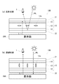
- FIG. 1 It is a schematic sectional drawing of the liquid crystal panel which concerns on one Embodiment of this invention.
- (A) is a figure for demonstrating a reflective state
- (b) is a figure for demonstrating a transmissive state.
- (A) It is a figure which shows the polarization degree of the absorption type polarizing plate of liquid crystal panels AE, the reflectance in a reflection state, and the reflectance in a permeation
- the liquid crystal panel 100 is a twisted nematic (TN (Twisted Nematic)) type liquid crystal panel, and is configured as shown in FIG. 1 in a schematic cross-sectional view.
- the liquid crystal panel 100 is configured to be switchable between a transmissive state and a reflective state.
- the liquid crystal panel 100 in the transmission state causes the viewer 1 to visually recognize the display image of the display unit 200 disposed behind the display panel 200 as it is.
- the liquid crystal panel 100 in the reflection state functions as a mirror for reflecting the external light NL and the like toward the observer 1 as shown in FIG. 2A.
- FIGS. 1 and 2 (a) and 2 (b) hatching indicating a cross section is omitted as appropriate in FIGS. 1 and 2 (a) and 2 (b). Further, in FIGS. 2A and 2B for describing the function of the liquid crystal panel 100, appropriate members are omitted.
- the liquid crystal panel 100 includes a liquid crystal element 10, an absorption type polarizing plate 21 located on the front side of the liquid crystal element 10, and a reflection type polarizing plate 22 located on the back side of the liquid crystal element 10.
- the liquid crystal panel 100 in a plan view has, for example, a substantially rectangular shape.
- the liquid crystal element 10 includes a first substrate 11, a second substrate 12, and a liquid crystal layer 13 as shown in FIG.
- the first substrate 11 and the second substrate 12 are a pair of transparent substrates facing each other, and are made of, for example, glass, plastic or the like.
- the first substrate 11 and the second substrate 12 are disposed so as to face each other with the liquid crystal layer 13 interposed therebetween, and such that the main surfaces (opposing surfaces) of the first substrate 11 and the second substrate 12 are parallel to each other.
- the first substrate 11 is located on the front side of the liquid crystal layer 13.
- a transparent electrode 11 a is provided on the liquid crystal layer 13 side of the first substrate 11.
- a transparent electrode 12 a is provided on the liquid crystal layer 13 side of the second substrate 12.
- the transparent electrodes 11a and 12a are formed by known methods such as sputtering, vapor deposition, and etching. In this embodiment, the transparent electrodes 11a and 12a are each formed solid on the corresponding substrate surface, and have a substantially rectangular shape in plan view.
- the transparent electrodes 11a and 12a are made of an ITO (Indium Tin Oxide) film or the like mainly composed of indium oxide.
- the application of the voltage to the liquid crystal layer 13 via the transparent electrodes 11a and 12a may be either a passive or active drive method.
- an insulating film and an alignment film are formed on each of the first substrate 11 and the second substrate 12.
- the insulating film is made of a silicon-based insulating film, and is formed so as to cover each of the transparent electrodes 11 a and 12 a from the liquid crystal layer 13 side.
- an alignment film is formed between the insulating film and the liquid crystal layer 13. That is, the transparent electrode 11 a, the insulating film, and the alignment film are stacked on the first substrate 11.
- a transparent electrode 12a, an insulating film, and an alignment film are laminated.
- the alignment film is in contact with the liquid crystal layer 13 and is for defining the alignment state of the liquid crystal molecules 13a (representatively shown in FIG. 2A and FIG. 2B) included in the liquid crystal layer 13. It is formed by a known method (for example, flexo printing).
- the alignment film is rubbed.
- the rubbing direction of the alignment film on the front side that is, the alignment film formed on the first substrate 11
- the rubbing direction of the back side that is, the alignment film formed on the second substrate 12
- they are substantially orthogonal (including exactly orthogonal).
- the alignment of the liquid crystal molecules 13a is regulated by the two alignment films subjected to the rubbing process as described above.
- the alignment treatment applied to the alignment film is not limited to the rubbing treatment, but may be another known treatment such as a photo alignment treatment or a projection alignment treatment.
- the liquid crystal layer 13 is formed by sealing a liquid crystal material in a sealed space formed by a sealing material (not shown) for bonding the first substrate 11 and the second substrate 12 and the two substrates.
- the thickness (cell gap) of the liquid crystal layer 13 is defined by a spacer (not shown) provided between the first substrate 11 and the second substrate 12.
- the orientation of the major axis of the liquid crystal molecules 13a of the liquid crystal layer 13 is twisted by 90 ° between the end of the liquid crystal layer 13 on the first substrate 11 side and the end of the liquid crystal layer 13 on the second substrate 12 side With a twist angle of 90 °), it is oriented so that it gradually rotates (turns) from one substrate side to the other substrate side (chiral structure).
- the liquid crystal layer 13 at the time of no voltage application has chirality.
- the absorption polarizing plate 21 has a transmission axis (hereinafter also referred to as a first transmission axis) and an absorption axis orthogonal to the first transmission axis.
- the absorption type polarizing plate 21 transmits light of the polarization direction parallel to the first transmission axis among the incident light.
- the reflective polarizing plate 22 has a transmission axis (hereinafter also referred to as a second transmission axis) and a reflection axis orthogonal to the second transmission axis.
- the reflective polarizing plate 22 transmits light of a polarization direction parallel to the second transmission axis among incident light, and reflects light of a polarization direction parallel to the reflection axis.
- the first transmission axis of the absorption polarizing plate 21 and the second transmission axis of the reflection polarizing plate 22 are substantially parallel to each other as viewed in the normal direction of the substrate. Both polarizing plates are arranged (parallel Nicol arrangement). Further, the rubbing direction of the alignment film on the front side (that is, the alignment film formed on the first substrate 11) and the direction along which the absorption axis of the absorption type polarizing plate 21 is parallel are set.
- the absorption polarizing plate 21 is attached to the front surface of the first substrate 11 via the first transparent adhesive film 31.
- the reflective polarizing plate 22 is attached to the rear surface of the second substrate 12 via the second transparent adhesive film 32.
- an optical element such as a retardation plate may be provided between the liquid crystal element 10 and each polarizing plate.
- the polarizing plate may be attached to an optical element located between the liquid crystal element 10 and the polarizing plate.
- the first transparent adhesive film 31 and the second transparent adhesive film 32 are each made of, for example, an acrylic transparent adhesive (acrylic polymer) or the like.
- the first transparent adhesive film 31 is formed by applying a transparent adhesive on the surface of the absorptive polarizing plate 21 to be attached to the first substrate 11.
- the second transparent adhesive film 32 is formed by applying a transparent adhesive on the surface of the reflective polarizing plate 22 to be attached to the second substrate 12.
- the liquid crystal panel 100 having the above configuration transmits the display light L (light representing a display image) of the display unit 200 as shown in FIG. 2B.
- the display unit 200 located on the back side of the liquid crystal panel 100 includes, for example, a liquid crystal display having a backlight and an organic electro luminescence (EL) display, and displays an image toward the liquid crystal panel 100.
- the target to be viewed through the liquid crystal panel 100 in the transmissive state is not limited to the display unit 200 that displays an image, and may be a dial, a sign, or a landscape.
- liquid crystal panel 100 can be switched between the reflection state and the transmission state as follows.
- the liquid crystal panel 100 functions as a mirror in the reflection state.
- a portion functioning as a mirror is referred to as an active area.
- the display light L when the display light L is incident from the back side of the liquid crystal panel 100, it passes through the reflective polarizing plate 22 and becomes linearly polarized light parallel to the second transmission axis, and when it passes through the liquid crystal layer 13, the 90 ° polarization direction is converted. Since the light is linearly polarized along the absorption axis of the absorption polarizing plate 21, it can not transmit through the absorption polarizing plate 21. As described above, since the display light L does not travel to the front side of the liquid crystal panel 100, even if the display light L is incident on the liquid crystal panel 100, the display image of the display unit 200 is not visually recognized by the observer 1. When the display light L exits the display unit 200, the display light L may be linearly polarized light parallel to the second transmission axis.
- the light passes through the absorbing polarizing plate 21 and passes through the liquid crystal layer 13 as linearly polarized light parallel to the first transmission axis, so that it is parallel to the first transmission axis.
- the light is transmitted through the reflective polarizing plate 22 having the second transmission axis and is not reflected by the reflective polarizing plate 22 (except for the reflection due to leaked light).
- the inventors of the present application paid attention to the fact that the reflectance of the liquid crystal display panel 100 changes with the degree of polarization of the absorption type polarizing plate 21, and in order to find suitable conditions for the degree of polarization, samples of five types of liquid crystal panels ( Liquid crystal panels A to E) shown in FIG. 3 (a) were produced.
- the liquid crystal panels A to E have the same configuration as the liquid crystal panel 100, but differ in the average degree of polarization of the absorption polarizing plate 21 at a wavelength of 450 nm to 650 nm.
- the “polarization degree” in FIG. 3 is an average polarization degree at a wavelength of 450 nm to 650 nm, more specifically, each wavelength of every 5 nm (450, 455,..., 645, 650) in a range of 450 nm to 650 nm. Indicates the average value of the degree of polarization of Hereinafter, the average degree of polarization at a wavelength of 450 nm to 650 nm is simply referred to as “degree of polarization”.
- each sample is created using the following materials.
- First substrate 11 and second substrate 12 thickness 1.1 mm glass substrate: made by Nippon Sheet Glass Co., Ltd.
- liquid crystal material made by AGC Seimi Chemical Co., Ltd.
- first transparent adhesive film 31 constituting liquid crystal layer 13
- second transparent adhesive Film 32 film thickness 25 ⁇ m: manufactured by Polatechno Co., Ltd.
- absorption polarizing plate 21 Patent Application Laidum (Poratechno Co.
- reflection polarizing plate 22 manufactured by 3M Co., DBEF.
- liquid crystal panel A has a degree of polarization of 57.7%
- liquid crystal panel B has a degree of polarization of 64.6%
- liquid crystal panel C has a degree of polarization of The degree of polarization is 72.5%
- the degree of polarization is 85.1% for the liquid crystal panel D
- the degree of polarization is 99.9% for the liquid crystal panel E.
- the total light reflectance of five types of samples (liquid crystal panels A to E) thus prepared was measured.
- the total light reflectance (hereinafter, also simply referred to as reflectance) is a ratio of light emitted again from the front side to all light incident from the front side (the absorption polarizing plate 21 side) of the liquid crystal panel.
- the reflectance was measured by an ultraviolet visible near infrared spectrophotometer U-4100 (manufactured by Hitachi High-Tech Science Co., Ltd.).
- the liquid crystal panel A has a reflectance of 45.4% in the reflection state and a reflectance of 12.5% in the transmission state. there were.
- the liquid crystal panel B had a reflectance of 45.3% in the reflective state and a reflectance of 10.6% in the transmissive state.
- the liquid crystal panel C had a reflectance of 42.5% in the reflection state and a reflectance of 8.6% in the transmission state.
- the liquid crystal panel D had a reflectance of 38.0% in the reflection state and a reflectance of 7.5% in the transmission state.
- the liquid crystal panel E had a reflectance of 34.7% in the reflection state and a 6.9% reflectance in the transmission state.
- the reflectance of the liquid crystal panel 100 in the reflection state is preferably 40% or more. This is to obtain a reflection image of sufficient brightness as a mirror.
- the reflectance is set to 35% or more.
- the reflectance of the liquid crystal panel 100 in the transmission state is preferably 12% or less, and more preferably 10% or less.
- the liquid crystal panel 100 has an average polarization degree of the absorption polarizing plate 21 at a wavelength of 450 nm to 650 nm.
- the reflectance in the reflection state is preferably 40% or more.
- the reflectance in the transmission state is 12% or less, which is a suitable reflectance.
- the reflectance in the transmission state is more preferably 10% or less. That is, the liquid crystal panel 100 has an average degree of polarization of 60% or more at a wavelength of 450 nm to 650 nm of the absorption type polarizing plate 21 in order to achieve both a suitable reflectance in the reflection state and a suitable reflectance in the transmission state. 80% or less is desirable, and 67% or more and 80% or less is more desirable.
- liquid crystal panel 100 by setting the average polarization degree of the absorption polarizing plate 21 at a wavelength of 450 nm to 650 nm to 60% or more and 80% or less, preferable total light reflectance in a reflection state And a suitable total light reflectance in the transmission state can be compatible.
- the liquid crystal panel 100 can obtain a more preferable total light reflectance in the transmission state by setting the average polarization degree of the absorption polarizing plate 21 at a wavelength of 450 nm to 650 nm to 67% or more. .
- the first transmission axis of the absorption polarizing plate 21 and the second transmission axis of the reflection polarizing plate 22 are set in parallel, and the liquid crystal panel 100 is in the reflection state when the drive voltage is not applied.
- the first transmission axis of the absorption polarizing plate 21 and the second transmission axis of the reflection polarizing plate 22 are set substantially orthogonal to each other so as to be in the reflection state when the drive voltage is applied, and the transmission state in the state where the drive voltage is not applied.
- the liquid crystal panel 100 may be configured to be (normally transmitted). In the example of normally transmission, the liquid crystal panel 100 can be switched between the reflection state and the transmission state as follows.
- This reflected light passes through the liquid crystal layer 13 again as it is, and passes through the absorbing polarizing plate 21 having a first transmission axis substantially orthogonal to the reflection axis.
- the liquid crystal panel 100 functions as a mirror in the reflection state.
- the display light L when the display light L is incident from the back side of the liquid crystal panel 100, it passes through the reflective polarizing plate 22 to become linearly polarized light parallel to the second transmission axis and passes through the liquid crystal layer 13 as it is. Can not be transmitted through the absorption type polarizing plate 21 having the following absorption axis.
- the display image of the display unit 200 is not visually recognized by the observer 1.
- the liquid crystal panel 100 transmits the display light L and causes the display image of the display unit 200 to be viewed through the water.
- the external light NL is incident from the front side of the liquid crystal panel 100, it passes through the absorbing polarizing plate 21 to be linearly polarized light parallel to the first transmission axis, and when it passes through the liquid crystal layer 13, 90 ° according to the chirality of the liquid crystal layer 13.
- the polarization direction is converted into linearly polarized light along a second transmission axis substantially orthogonal to the reflection axis of the reflection type polarizing plate 22 parallel to the first transmission axis, and transmitted through the reflection type polarizing plate 22 having the second transmission axis. , And not reflected by the reflection type polarizing plate 22 (except for reflection by leaked light).
- the application of the liquid crystal panel 100 is also arbitrary.
- Watch or portable terminal for example, information display is performed by the display unit 200 on the back side of the liquid crystal panel 100 in the transmission state, functions as a mirror in the reflection state
- transmission / reflection control of a predetermined window for example, the view in the transmission state Window, which functions as a mirror in the reflection state, and various side mirrors and rearview mirrors of the car (for example, vehicle information and camera images are displayed by the display unit 200 on the back side of the liquid crystal panel 100 in the transmission state) It is applicable to the use.
- liquid crystal panel 100 when viewed from the substrate normal direction is substantially rectangular in the above description, it may be circular, polygonal or the like, and the shape is arbitrary according to the application. Similarly, the shape of the transparent electrodes 11a and 12a when viewed from the substrate normal direction is also arbitrary.
- the liquid crystal element 10 is a TN liquid crystal having a twist angle of 90 °
- the twist angle may be less than 90 ° or greater than 90 ° as long as the reflection state and the transmission state described above can be realized according to the application of a voltage to the liquid crystal layer 13.
- the liquid crystal element 10 may be of the STN (Super Twisted Nematic) type.
- the first transmission axis of the absorptive polarizer 21 and the second transmission axis of the reflective polarizer 22 are The relationship between the optical axis and the rubbing direction of the alignment film may not be parallel or orthogonal. It is also possible to shift each optical axis appropriately in consideration of the viewing angle characteristics in the transmission state and the reflection characteristics in the reflection state.
- liquid crystal panel 10 liquid crystal element 11 first substrate 11a transparent electrode 12 second substrate 12a transparent electrode 13 liquid crystal layer 13a liquid crystal molecule 21 absorption type polarizing plate 22 reflection type polarizing plate 31: first transparent adhesive film 32: second transparent adhesive film
Abstract
Description
液晶層と、前記液晶層に前記電圧を印加するための透明電極とを含む液晶素子と、
前記液晶素子の一方側に設けられた吸収型偏光板と、
前記液晶素子の他方側に設けられ、前記吸収型偏光板と前記液晶素子を挟んで対向する反射型偏光板と、を備え、
前記反射状態においては、前記吸収型偏光板側から入射して前記液晶素子を透過した光が、前記反射型偏光板の反射軸に沿う偏光軸の光となり、前記反射型偏光板で反射され、
前記透過状態においては、前記吸収型偏光板側から入射して前記液晶素子を透過した光が、前記反射型偏光板の反射軸と交差する透過軸に沿う偏光軸の光となり、前記反射型偏光板を透過し、
前記吸収型偏光板は、450nm~650nmの波長での平均偏光度が60%以上かつ80%以下である、
ことを特徴とする。 In order to achieve the above object, a liquid crystal panel according to a first aspect of the present invention is a liquid crystal panel that switches between a transmission state and a reflection state according to application of a voltage,
A liquid crystal element including a liquid crystal layer, and a transparent electrode for applying the voltage to the liquid crystal layer;
An absorption polarizing plate provided on one side of the liquid crystal element;
And a reflective polarizing plate provided on the other side of the liquid crystal element and facing the absorption polarizing plate with the liquid crystal element interposed therebetween.
In the reflection state, light incident from the absorption type polarizing plate side and transmitted through the liquid crystal element becomes light of a polarization axis along a reflection axis of the reflection type polarization plate, and is reflected by the reflection type polarization plate,
In the transmission state, light incident from the absorption polarizing plate side and transmitted through the liquid crystal element becomes light of a polarization axis along a transmission axis intersecting the reflection axis of the reflection polarizing plate, and the reflection polarization Permeate the plate,
The absorption polarizing plate has an average degree of polarization of 60% to 80% at a wavelength of 450 nm to 650 nm.
It is characterized by
駆動電圧が印加されていない状態では、液晶表示素子100では、図2(a)に示すように、液晶分子13aが実質的に基板面と平行であり、液晶層13はカイラリティを有したままである。この状態で、外光NLが液晶パネル100の表側から入射すると、吸収型偏光板21を透過して第1透過軸と平行な直線偏光となり、液晶層13を透過すると、液晶層13のカイラリティにより90°偏光方向が変換されて、反射型偏光板22の反射軸に沿う直線偏光となるため、反射型偏光板22で反射される。この反射光は、液晶層13を透過して、再び偏光方向が90°変換されるため、吸収型偏光板21を透過する。このようにして、液晶パネル100は、反射状態においては鏡として機能する。以下では、反射状態の液晶パネル100のうち、鏡として機能する部分をアクティブエリアと呼ぶ。 (Reflection state)
When no driving voltage is applied, in the liquid
駆動電圧の印加時においては、液晶パネル100では、図2(b)に示すように、液晶分子13aは、電圧の印加方向(基板法線方向)に沿うように配向し、そのカイラリティが失われる。この状態で、表示光Lが液晶パネル100の裏側から入射すると、反射型偏光板22を透過して第2透過軸と平行な直線偏光となるが、液晶層13を透過しても偏光方向は変換されないため、第2透過軸と平行な第1透過軸を有する吸収型偏光板21を透過する。このようにして、液晶パネル100は、表示光Lを透過させ、表示部200の表示画像を透かして視認させる。
なお、外光NLが液晶パネル100の表側から入射すると、吸収型偏光板21を透過して第1透過軸と平行な直線偏光のまま液晶層13を透過するため、第1透過軸と平行な第2透過軸を有する反射型偏光板22を透過し、反射型偏光板22では反射しない(漏れ光による反射は除く)。 (Transparent state)
At the time of application of the drive voltage, as shown in FIG. 2B, in the
When the external light NL is incident from the front side of the
(2)また、液晶パネル100は、吸収型偏光板21の450nm~650nmの波長での平均偏光度を67%以上とすることにより、透過状態における更に好適な全光反射率を得ることができる。 (1) In the
(2) Further, the
駆動電圧の印加時においては、液晶パネル100では、前述のように、液晶分子13aは、電圧の印加方向(基板法線方向)に沿うように配向し、そのカイラリティが失われる。この状態で、外光NLが液晶パネル100の表側から入射すると、吸収型偏光板21を透過して第1透過軸と平行な直線偏光のまま液晶層13を透過するため、第1透過軸と平行な反射型偏光板22の反射軸に沿う直線偏光となり、反射型偏光板22で反射される。この反射光は、そのまま再び液晶層13を透過して、反射軸と略直交する第1透過軸を有する吸収型偏光板21を透過する。このようにして、液晶パネル100は、反射状態においては鏡として機能する。
一方、表示光Lが液晶パネル100の裏側から入射すると、反射型偏光板22を透過して第2透過軸と平行な直線偏光となり、そのまま液晶層13を透過するため、第2透過軸と平行な吸収軸を有する吸収型偏光板21を透過できない。このように、表示光Lは液晶パネル100の表側には進めないため、仮に表示光Lが液晶パネル100に入射したとしても表示部200の表示画像は観察者1に視認されない。 (Reflection state)
When the drive voltage is applied, as described above, in the
On the other hand, when the display light L is incident from the back side of the
駆動電圧が印加されていない状態では、液晶パネル100では、前述のように、液晶分子13aが実質的に基板面と平行であり、液晶層13はカイラリティを有したままである。この状態で、表示光Lが液晶パネル100の裏側から入射すると、反射型偏光板22を透過して第2透過軸と平行な直線偏光となり、液晶層13を透過すると、液晶層13のカイラリティにより90°偏光方向が変換されて、第2透過軸と略直交する第1透過軸を有する吸収型偏光板21を透過する。このようにして、液晶パネル100は、表示光Lを透過させ、表示部200の表示画像を透かして視認させる。
なお、外光NLが液晶パネル100の表側から入射すると、吸収型偏光板21を透過して第1透過軸と平行な直線偏光となり、液晶層13を透過すると、液晶層13のカイラリティにより90°偏光方向が変換されて、第1透過軸と平行な反射型偏光板22の反射軸と略直交する第2透過軸に沿う直線偏光となり、第2透過軸を有する反射型偏光板22を透過し、反射型偏光板22では反射しない(漏れ光による反射は除く)。 (Transparent state)
In the state where the drive voltage is not applied, in the
When the external light NL is incident from the front side of the
10…液晶素子
11…第1基板、11a…透明電極、12…第2基板、12a…透明電極
13…液晶層、13a…液晶分子
21…吸収型偏光板
22…反射型偏光板
31…第1透明粘着膜
32…第2透明粘着膜 100
Claims (2)
- 電圧の印加に応じて透過状態と反射状態とに切り替わる液晶パネルであって、
液晶層と、前記液晶層に前記電圧を印加するための透明電極とを含む液晶素子と、
前記液晶素子の一方側に設けられた吸収型偏光板と、
前記液晶素子の他方側に設けられ、前記吸収型偏光板と前記液晶素子を挟んで対向する反射型偏光板と、を備え、
前記反射状態においては、前記吸収型偏光板側から入射して前記液晶素子を透過した光が、前記反射型偏光板の反射軸に沿う偏光軸の光となり、前記反射型偏光板で反射され、
前記透過状態においては、前記吸収型偏光板側から入射して前記液晶素子を透過した光が、前記反射型偏光板の反射軸と交差する透過軸に沿う偏光軸の光となり、前記反射型偏光板を透過し、
前記吸収型偏光板は、450nm~650nmの波長での平均偏光度が60%以上かつ80%以下である、
ことを特徴とする液晶パネル。 A liquid crystal panel that switches between a transmissive state and a reflective state according to the application of a voltage,
A liquid crystal element including a liquid crystal layer, and a transparent electrode for applying the voltage to the liquid crystal layer;
An absorption polarizing plate provided on one side of the liquid crystal element;
And a reflective polarizing plate provided on the other side of the liquid crystal element and facing the absorption polarizing plate with the liquid crystal element interposed therebetween.
In the reflection state, light incident from the absorption type polarizing plate side and transmitted through the liquid crystal element becomes light of a polarization axis along a reflection axis of the reflection type polarization plate, and is reflected by the reflection type polarization plate,
In the transmission state, light incident from the absorption polarizing plate side and transmitted through the liquid crystal element becomes light of a polarization axis along a transmission axis intersecting the reflection axis of the reflection polarizing plate, and the reflection polarization Permeate the plate,
The absorption polarizing plate has an average degree of polarization of 60% to 80% at a wavelength of 450 nm to 650 nm.
A liquid crystal panel characterized by - 前記吸収型偏光板は、450nm~650nmの波長での平均偏光度が67%以上である、
ことを特徴とする請求項1に記載の液晶パネル。 The absorption polarizing plate has an average degree of polarization of 67% or more at a wavelength of 450 nm to 650 nm.
The liquid crystal panel according to claim 1,
Priority Applications (4)
| Application Number | Priority Date | Filing Date | Title |
|---|---|---|---|
| US16/623,631 US10782555B2 (en) | 2017-06-23 | 2018-06-20 | Liquid crystal panel |
| JP2019525651A JPWO2018235847A1 (en) | 2017-06-23 | 2018-06-20 | LCD panel |
| EP18820835.9A EP3644112A4 (en) | 2017-06-23 | 2018-06-20 | Liquid crystal panel |
| CN201880040892.4A CN110770642B (en) | 2017-06-23 | 2018-06-20 | Liquid crystal panel |
Applications Claiming Priority (2)
| Application Number | Priority Date | Filing Date | Title |
|---|---|---|---|
| JP2017122841 | 2017-06-23 | ||
| JP2017-122841 | 2017-06-23 |
Publications (1)
| Publication Number | Publication Date |
|---|---|
| WO2018235847A1 true WO2018235847A1 (en) | 2018-12-27 |
Family
ID=64735622
Family Applications (1)
| Application Number | Title | Priority Date | Filing Date |
|---|---|---|---|
| PCT/JP2018/023385 WO2018235847A1 (en) | 2017-06-23 | 2018-06-20 | Liquid crystal panel |
Country Status (5)
| Country | Link |
|---|---|
| US (1) | US10782555B2 (en) |
| EP (1) | EP3644112A4 (en) |
| JP (1) | JPWO2018235847A1 (en) |
| CN (1) | CN110770642B (en) |
| WO (1) | WO2018235847A1 (en) |
Citations (3)
| Publication number | Priority date | Publication date | Assignee | Title |
|---|---|---|---|---|
| JP2001318374A (en) * | 2000-02-29 | 2001-11-16 | Hitachi Ltd | Device which can be switched between image display state and mirror state and apparatus equipped with the same |
| US20150049283A1 (en) * | 2013-08-19 | 2015-02-19 | Samsung Electronics Co., Ltd. | Display apparatus and control method thereof |
| WO2017073498A1 (en) * | 2015-10-30 | 2017-05-04 | シャープ株式会社 | Switching mirror panel and switching mirror device |
Family Cites Families (10)
| Publication number | Priority date | Publication date | Assignee | Title |
|---|---|---|---|---|
| JP3186070B2 (en) * | 1997-07-30 | 2001-07-11 | シチズン時計株式会社 | Liquid crystal display |
| JP3580124B2 (en) * | 1998-03-05 | 2004-10-20 | 日東電工株式会社 | Optical element, lighting device and liquid crystal display device |
| JPH11316372A (en) * | 1998-04-30 | 1999-11-16 | Seiko Epson Corp | Liquid crystal device and electronic equipment |
| US7495719B2 (en) * | 2001-02-28 | 2009-02-24 | Hitachi Displays, Ltd. | Device capable of switching between an image display status and a mirror status, and an instrument disposed therewith |
| US7894019B2 (en) * | 2005-10-17 | 2011-02-22 | Asahi Kasei Kabushiki Kaisha | Wire grid polarizer and liquid crystal display device using the same |
| JP4275692B2 (en) * | 2005-10-17 | 2009-06-10 | 旭化成株式会社 | Wire grid polarizer and liquid crystal display using the same |
| TW201009401A (en) * | 2008-07-04 | 2010-03-01 | Mitsui Chemicals Inc | Polarizing diffuser film and fabricating method thereof and liquid crystal display device including polarizing diffuser film |
| US9519090B2 (en) * | 2012-09-24 | 2016-12-13 | Teijin Limited | Uniaxially stretched multi-layer laminate film, polarizing plate comprising same, optical member for liquid crystal display device, and liquid crystal display device |
| EP3121627A4 (en) * | 2014-03-19 | 2017-04-12 | Teijin Limited | Reflective polarizing film for liquid-crystal-display polarizer, liquid-crystal-display polarizer comprising same, liquid-crystal-display optical element, and liquid-crystal display |
| JP6815249B2 (en) * | 2017-03-29 | 2021-01-20 | 株式会社ジャパンディスプレイ | Display device |
-
2018
- 2018-06-20 EP EP18820835.9A patent/EP3644112A4/en not_active Withdrawn
- 2018-06-20 US US16/623,631 patent/US10782555B2/en active Active
- 2018-06-20 CN CN201880040892.4A patent/CN110770642B/en active Active
- 2018-06-20 JP JP2019525651A patent/JPWO2018235847A1/en active Pending
- 2018-06-20 WO PCT/JP2018/023385 patent/WO2018235847A1/en active Application Filing
Patent Citations (4)
| Publication number | Priority date | Publication date | Assignee | Title |
|---|---|---|---|---|
| JP2001318374A (en) * | 2000-02-29 | 2001-11-16 | Hitachi Ltd | Device which can be switched between image display state and mirror state and apparatus equipped with the same |
| JP3419766B2 (en) | 2000-02-29 | 2003-06-23 | 株式会社日立製作所 | Apparatus that can switch between image display state and mirror state, and equipment equipped with this |
| US20150049283A1 (en) * | 2013-08-19 | 2015-02-19 | Samsung Electronics Co., Ltd. | Display apparatus and control method thereof |
| WO2017073498A1 (en) * | 2015-10-30 | 2017-05-04 | シャープ株式会社 | Switching mirror panel and switching mirror device |
Non-Patent Citations (1)
| Title |
|---|
| See also references of EP3644112A4 |
Also Published As
| Publication number | Publication date |
|---|---|
| JPWO2018235847A1 (en) | 2020-04-23 |
| EP3644112A1 (en) | 2020-04-29 |
| CN110770642A (en) | 2020-02-07 |
| US10782555B2 (en) | 2020-09-22 |
| US20200192155A1 (en) | 2020-06-18 |
| CN110770642B (en) | 2022-06-14 |
| EP3644112A4 (en) | 2021-02-24 |
Similar Documents
| Publication | Publication Date | Title |
|---|---|---|
| US10023123B2 (en) | Image display mirror for a vehicle | |
| JP6571935B2 (en) | Video display mirror for vehicles | |
| WO2002006863A1 (en) | Circular polarization plate and liquid crystal display device | |
| JP4125876B2 (en) | Transflective liquid crystal display device | |
| US10207645B2 (en) | Vehicle including mirror with image display apparatus | |
| JP2005352068A (en) | Liquid crystal display device | |
| US9868400B2 (en) | Image display mirror for a vehicle | |
| JP5203557B2 (en) | Liquid crystal display | |
| WO2018116895A1 (en) | Liquid crystal panel | |
| JPH11231303A (en) | Liquid crystal display device | |
| WO2018235847A1 (en) | Liquid crystal panel | |
| JP2796212B2 (en) | Liquid crystal display | |
| JP3760656B2 (en) | Liquid crystal device and electronic device | |
| JP2005164957A (en) | Circularly polarizing plate and liquid crystal display element | |
| JP2018180471A (en) | Liquid crystal panel | |
| JP2018180470A (en) | Liquid crystal panel | |
| JP2021036281A (en) | Liquid crystal panel | |
| JP2004061765A (en) | Liquid crystal display | |
| JP2000258773A (en) | Reflection type liquid crystal display device | |
| JP2005241802A (en) | Liquid crystal display device | |
| JP2001318378A (en) | Reflection liquid crystal display element | |
| JPH01188831A (en) | Liquid crystal display device | |
| JP2010044145A (en) | Liquid crystal device |
Legal Events
| Date | Code | Title | Description |
|---|---|---|---|
| 121 | Ep: the epo has been informed by wipo that ep was designated in this application |
Ref document number: 18820835 Country of ref document: EP Kind code of ref document: A1 |
|
| ENP | Entry into the national phase |
Ref document number: 2019525651 Country of ref document: JP Kind code of ref document: A |
|
| NENP | Non-entry into the national phase |
Ref country code: DE |
|
| WWE | Wipo information: entry into national phase |
Ref document number: 2018820835 Country of ref document: EP |
|
| ENP | Entry into the national phase |
Ref document number: 2018820835 Country of ref document: EP Effective date: 20200123 |