WO2018221351A1 - Light emitting device, projector, and a light emitting device manufacturing method - Google Patents
Light emitting device, projector, and a light emitting device manufacturing method Download PDFInfo
- Publication number
- WO2018221351A1 WO2018221351A1 PCT/JP2018/019841 JP2018019841W WO2018221351A1 WO 2018221351 A1 WO2018221351 A1 WO 2018221351A1 JP 2018019841 W JP2018019841 W JP 2018019841W WO 2018221351 A1 WO2018221351 A1 WO 2018221351A1
- Authority
- WO
- WIPO (PCT)
- Prior art keywords
- light emitting
- emitting device
- base
- electrode
- light
- Prior art date
Links
Images


Classifications
-
- H—ELECTRICITY
- H01—ELECTRIC ELEMENTS
- H01L—SEMICONDUCTOR DEVICES NOT COVERED BY CLASS H10
- H01L33/00—Semiconductor devices with at least one potential-jump barrier or surface barrier specially adapted for light emission; Processes or apparatus specially adapted for the manufacture or treatment thereof or of parts thereof; Details thereof
- H01L33/02—Semiconductor devices with at least one potential-jump barrier or surface barrier specially adapted for light emission; Processes or apparatus specially adapted for the manufacture or treatment thereof or of parts thereof; Details thereof characterised by the semiconductor bodies
- H01L33/20—Semiconductor devices with at least one potential-jump barrier or surface barrier specially adapted for light emission; Processes or apparatus specially adapted for the manufacture or treatment thereof or of parts thereof; Details thereof characterised by the semiconductor bodies with a particular shape, e.g. curved or truncated substrate
- H01L33/24—Semiconductor devices with at least one potential-jump barrier or surface barrier specially adapted for light emission; Processes or apparatus specially adapted for the manufacture or treatment thereof or of parts thereof; Details thereof characterised by the semiconductor bodies with a particular shape, e.g. curved or truncated substrate of the light emitting region, e.g. non-planar junction
-
- H—ELECTRICITY
- H01—ELECTRIC ELEMENTS
- H01L—SEMICONDUCTOR DEVICES NOT COVERED BY CLASS H10
- H01L33/00—Semiconductor devices with at least one potential-jump barrier or surface barrier specially adapted for light emission; Processes or apparatus specially adapted for the manufacture or treatment thereof or of parts thereof; Details thereof
- H01L33/005—Processes
- H01L33/0095—Post-treatment of devices, e.g. annealing, recrystallisation or short-circuit elimination
-
- H—ELECTRICITY
- H01—ELECTRIC ELEMENTS
- H01L—SEMICONDUCTOR DEVICES NOT COVERED BY CLASS H10
- H01L33/00—Semiconductor devices with at least one potential-jump barrier or surface barrier specially adapted for light emission; Processes or apparatus specially adapted for the manufacture or treatment thereof or of parts thereof; Details thereof
- H01L33/02—Semiconductor devices with at least one potential-jump barrier or surface barrier specially adapted for light emission; Processes or apparatus specially adapted for the manufacture or treatment thereof or of parts thereof; Details thereof characterised by the semiconductor bodies
- H01L33/08—Semiconductor devices with at least one potential-jump barrier or surface barrier specially adapted for light emission; Processes or apparatus specially adapted for the manufacture or treatment thereof or of parts thereof; Details thereof characterised by the semiconductor bodies with a plurality of light emitting regions, e.g. laterally discontinuous light emitting layer or photoluminescent region integrated within the semiconductor body
-
- H—ELECTRICITY
- H01—ELECTRIC ELEMENTS
- H01L—SEMICONDUCTOR DEVICES NOT COVERED BY CLASS H10
- H01L33/00—Semiconductor devices with at least one potential-jump barrier or surface barrier specially adapted for light emission; Processes or apparatus specially adapted for the manufacture or treatment thereof or of parts thereof; Details thereof
- H01L33/36—Semiconductor devices with at least one potential-jump barrier or surface barrier specially adapted for light emission; Processes or apparatus specially adapted for the manufacture or treatment thereof or of parts thereof; Details thereof characterised by the electrodes
- H01L33/38—Semiconductor devices with at least one potential-jump barrier or surface barrier specially adapted for light emission; Processes or apparatus specially adapted for the manufacture or treatment thereof or of parts thereof; Details thereof characterised by the electrodes with a particular shape
-
- H—ELECTRICITY
- H01—ELECTRIC ELEMENTS
- H01L—SEMICONDUCTOR DEVICES NOT COVERED BY CLASS H10
- H01L33/00—Semiconductor devices with at least one potential-jump barrier or surface barrier specially adapted for light emission; Processes or apparatus specially adapted for the manufacture or treatment thereof or of parts thereof; Details thereof
- H01L33/48—Semiconductor devices with at least one potential-jump barrier or surface barrier specially adapted for light emission; Processes or apparatus specially adapted for the manufacture or treatment thereof or of parts thereof; Details thereof characterised by the semiconductor body packages
- H01L33/62—Arrangements for conducting electric current to or from the semiconductor body, e.g. lead-frames, wire-bonds or solder balls
-
- H—ELECTRICITY
- H01—ELECTRIC ELEMENTS
- H01L—SEMICONDUCTOR DEVICES NOT COVERED BY CLASS H10
- H01L33/00—Semiconductor devices with at least one potential-jump barrier or surface barrier specially adapted for light emission; Processes or apparatus specially adapted for the manufacture or treatment thereof or of parts thereof; Details thereof
- H01L33/48—Semiconductor devices with at least one potential-jump barrier or surface barrier specially adapted for light emission; Processes or apparatus specially adapted for the manufacture or treatment thereof or of parts thereof; Details thereof characterised by the semiconductor body packages
- H01L33/64—Heat extraction or cooling elements
- H01L33/647—Heat extraction or cooling elements the elements conducting electric current to or from the semiconductor body
-
- H—ELECTRICITY
- H01—ELECTRIC ELEMENTS
- H01L—SEMICONDUCTOR DEVICES NOT COVERED BY CLASS H10
- H01L2933/00—Details relating to devices covered by the group H01L33/00 but not provided for in its subgroups
- H01L2933/0008—Processes
- H01L2933/0033—Processes relating to semiconductor body packages
Definitions
- the present invention relates to a light emitting device, a projector, and a method for manufacturing the light emitting device.
- junction-down mounting is known as a mounting method for light emitting elements such as semiconductor lasers and light emitting diodes. By junction-down mounting the light emitting element, heat generated in the light emitting element can be efficiently dissipated.
- Patent Document 1 discloses a light-emitting element in which a surface electrode of a laser chip is bonded to a mount serving as a heat sink with a solder material and junction-down mounted.
- the laser chip is provided on the substrate, the active layer formed on the substrate including the lower cladding layer, the quantum well layer, and the upper cladding layer, the surface electrode formed on the active layer, and the back surface of the substrate And a back electrode.
- the light emitting device is A light emitting device including a first substrate provided with a laminate; A second substrate provided with the light emitting element; A first member provided between the first base and the second base,
- the laminate includes a light emitting unit, The light emitting unit A first semiconductor layer; A second semiconductor layer having a conductivity type different from that of the first semiconductor layer; A light emitting layer provided between the first semiconductor layer and the second semiconductor layer and capable of emitting light when a current is injected;
- the first member has one end connected to the first base and the other end connected to the second base.
- the laminate is connected to the second base on the side opposite to the first base.
- such a light emitting device includes a first member having one end connected to the first base and the other end connected to the second base, the stack is connected to the second base in the manufacturing process (that is, the stack).
- the force applied to the light-emitting element including the light-emitting element when mounted on the second substrate is dispersed in the laminate and the first member. Therefore, in such a light emitting device, it is possible to reduce the pressure applied to the light emitting unit (laminated body) during mounting. As a result, it is possible to reduce the possibility of stress and distortion occurring in the light emitting portion (laminated body), and to realize a highly reliable light emitting device having stable light emitting characteristics.
- the first member may be provided so as to surround the periphery of the stacked body.
- the laminate may be hermetically sealed with the first member, the first base, and the second base.
- the device can be reduced in size and the manufacturing process can be simplified as compared with a case where the light emitting element is hermetically sealed with a package such as a ceramic package or a CAN package.
- the first member may be conductive and electrically connected to the first semiconductor layer.
- the first member can also function as an electrode for injecting current into the first semiconductor layer.
- the second member may have one end connected to the first base and the other end connected to the second base.
- the force applied during mounting is distributed to the stacked body, the first member, and the second member, so that the pressure applied to the light-emitting portion (laminated body) during mounting can be further reduced.
- the second member may surround the first member and the laminate.
- the second substrate may be provided with a penetrating electrode that penetrates the second substrate.
- the laminate (light-emitting portion) hermetically sealed by the first member, the first base, and the second base can be electrically connected to the external power supply device.
- the second semiconductor layer may be electrically connected to the through electrode.
- the first member, the first base, and the second semiconductor layer included in the stacked body (light emitting portion) hermetically sealed by the second base are electrically connected to the external power supply device. Can be connected to.
- the laminate has a plurality of columnar parts
- the light emitting unit may be composed of the plurality of columnar parts.
- Such a light emitting device In such a light emitting device, dislocations and defects generated in the first semiconductor layer, the light emitting layer, and the second semiconductor layer can be reduced, and high quality crystals can be obtained. Therefore, such a light emitting device can have excellent light emission characteristics.
- the first member may be connected to the second base via a bonding member.
- the first member can be reliably connected (joined) to the second base.
- the projector according to the present invention includes the light emitting device according to the present invention.
- Such a projector can include the light emitting device according to the present invention.
- a method for manufacturing a light emitting device includes: Forming a laminate including a light emitting portion on the first substrate; Forming a first member on the first base; Connecting the laminate formed on the first base and the first member to a second base, and The light emitting unit A first semiconductor layer; A second semiconductor layer having a conductivity type different from that of the first semiconductor layer; A light emitting layer provided between the first semiconductor layer and the second semiconductor layer and capable of emitting light when a current is injected.
- the force applied during mounting is laminated. Dispersed in the body and the first member. Therefore, the pressure applied to the light emitting part (laminated body) at the time of mounting can be reduced. As a result, the possibility of stress and distortion occurring in the light emitting portion (laminated body) can be reduced, and a highly reliable light emitting device having stable light emitting characteristics can be manufactured.
- Sectional drawing which shows typically the light-emitting device which concerns on 1st Embodiment.
- the top view which shows typically the light-emitting device which concerns on 1st Embodiment.
- 5 is a flowchart showing an example of a method for manufacturing the light emitting device according to the first embodiment.
- Sectional drawing which shows typically the manufacturing process of the light-emitting device which concerns on 2nd Embodiment. Sectional drawing which shows typically the manufacturing process of the light-emitting device which concerns on 2nd Embodiment. Sectional drawing which shows typically the manufacturing process of the light-emitting device which concerns on 2nd Embodiment. Sectional drawing which shows typically the manufacturing process of the light-emitting device which concerns on the modification of 2nd Embodiment. Sectional drawing which shows typically the light-emitting device which concerns on 3rd Embodiment. The top view which shows typically the light-emitting device which concerns on 3rd Embodiment. 9 is a flowchart illustrating an example of a method for manufacturing a light emitting device according to a third embodiment.
- FIG. 10 schematically illustrates a projector according to a sixth embodiment.
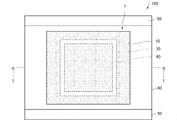
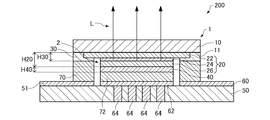
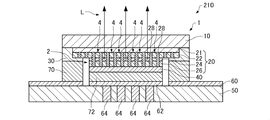
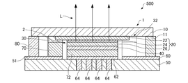
- FIG. 1 is a cross-sectional view schematically showing a light emitting device 100 according to the first embodiment.
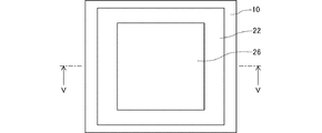
- FIG. 2 is a plan view schematically showing the light emitting device 100 according to the first embodiment.
- 1 is a cross-sectional view taken along the line II of FIG.
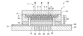
- the light emitting device 100 includes a light emitting element 1 having a first base 10, a laminate 20, a first electrode 30 (first member), and a second electrode 40, and a second base 50. Including.
- the first base 10, the stacked body 20, the first electrode 30, and the second electrode 40 constitute the light emitting element 1, and the light emitting element 1 is junction-down mounted on the second base 50 (mounting substrate). Yes.
- the first base 10 has, for example, a plate shape.
- the first base 10 is, for example, a sapphire substrate.
- the first substrate 10 is transparent to the light L generated in the light emitting layer 24. Therefore, the light L generated in the light emitting layer 24 passes through the first base 10 and is emitted to the outside. That is, the light emitting device 100 emits light L from the first base 10 side.
- substrate 10 is not limited to a sapphire substrate, Other ceramic substrates, a glass substrate, etc. can be used.
- the laminate 20 is provided on the first base 10.
- the stacked body 20 is provided on the main surface 11 of the first base 10.
- the stacked body 20 is located between the first base 10 and the second base 50.
- the stacked body 20 is composed of a plurality of layers stacked on the main surface 11 of the first base 10.
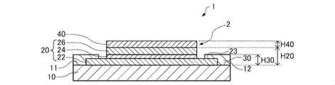
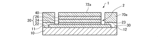
- the stacked body 20 includes the light emitting unit 2.
- the light emitting unit 2 includes a first semiconductor layer 22, a light emitting layer 24, and a second semiconductor layer 26.
- the light emitting element 1 is mounted on the second base 50 in a junction-down manner. That is, in the light emitting device 100, the stacked body 20 is connected to the second base 50 on the opposite side of the first base 10. The stacked body 20 is connected to the second base body 50 (second wiring 62) via the second electrode 40 and the bonding member 72.
- connection means, for example, “a specific thing (hereinafter referred to as“ A ”) is connected to another specific thing (hereinafter referred to as“ B ”)”.
- A is connected to B directly (A and B are in contact), and A is connected to B through another And the word “connection” is used.
- the word “provide” means, for example, “a specific thing (hereinafter referred to as“ C ”) is provided in another specific thing (hereinafter referred to as“ D ”)”.
- C is provided directly to D (C and D are in contact with each other), and C is provided to D via another And the word “provide” is used.
- the first semiconductor layer 22 is provided on the first base 10.
- the first semiconductor layer 22 is provided between the first base 10 and the light emitting layer 24.
- the first semiconductor layer 22 is, for example, a first conductivity type (for example, n-type) GaN layer (specifically, a GaN layer doped with Si).
- a buffer layer may be provided between the first semiconductor layer 22 and the first base 10.
- the buffer layer is, for example, an undoped GaN layer.
- the light emitting layer 24 is provided between the first semiconductor layer 22 and the second semiconductor layer 26.
- the light emitting layer 24 is a layer capable of emitting light when current is injected.
- the light emitting layer 24 has, for example, a quantum well structure composed of a GaN layer and an InGaN layer.
- the number of GaN layers and InGaN layers constituting the light emitting layer 24 is not particularly limited.
- the second semiconductor layer 26 is provided between the light emitting layer 24 and the second electrode 40.
- the second semiconductor layer 26 is a layer having a different conductivity type from the first semiconductor layer 22.
- the second semiconductor layer 26 is, for example, a second conductivity type (for example, p-type) GaN layer (specifically, a GaN layer doped with Mg).
- a pin diode is formed by the p-type second semiconductor layer 26, the light emitting layer 24 not doped with impurities, and the n-type first semiconductor layer 22.
- Each of the first semiconductor layer 22 and the second semiconductor layer 26 is a layer having a band gap larger than that of the light emitting layer 24.
- the light L generated in the light emitting layer 24 passes through the first base 10 and is emitted in the stacking direction of the stacked body 20 (hereinafter also simply referred to as “stacking direction”).
- the light emitting element 1 is a light emitting diode (LED).
- the first electrode 30 is provided between the first base 10 and the second base 50.
- the first electrode 30 has one end connected to the first base 10 and the other end connected to the second base 50.
- the first electrode 30 and the first base 10 remove the first semiconductor layer 22 provided on the first base 10 and form the first electrode 30 directly on the first base 10. Connected by that.
- One end of the first electrode 30 is further connected to the first semiconductor layer 22.
- the first electrode 30 and the second base body 50 are joined via a joining member 70.
- the first electrode 30 and the second substrate 50 are connected by bonding the first electrode 30 to the first wiring 60 provided on the second substrate 50 with a bonding member 70.
- the first electrode 30 is electrically connected to the first semiconductor layer 22.
- the first electrode 30 is electrically connected to the first wiring 60.
- the first electrode 30 is one electrode for injecting current into the light emitting layer 24.
- a metal layer such as an Au layer or an Ag layer, or a layer in which a Cr layer, a Ni layer, and an Au layer are stacked in this order from the first base 10 and the first semiconductor layer 22 side is used.
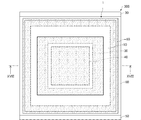
- the first electrode 30 surrounds the periphery of the stacked body 20 in a plan view (viewed from the stacking direction).
- the first electrode 30 is provided along the outer edge of the stacked body 20 in plan view. In plan view, a part of the first electrode 30 overlaps the outer edge portion of the first semiconductor layer 22.
- the first electrode 30 has a rectangular tube shape.
- a space for accommodating the stacked body 20 in an airtight manner is formed. That is, the stacked body 20 is hermetically sealed by the first electrode 30, the first base 10, and the second base 50.
- the space in which the stacked body 20 is accommodated is, for example, an inert gas atmosphere.
- the second electrode 40 is provided on the opposite side of the laminate 20 from the first base 10 side.
- the second electrode 40 is provided between the stacked body 20 and the second wiring 62 (second base body 50).
- the second electrode 40 is electrically connected to the second semiconductor layer 26.
- the second electrode 40 is electrically connected to the second wiring 62. Therefore, the second semiconductor layer 26 is electrically connected to the through electrode 64 via the second electrode 40 and the second wiring 62.
- the second electrode 40 is the other electrode for injecting current into the light emitting layer 24.
- a metal layer such as an Au layer or an Ag layer, or a layer in which a Pd layer, a Pt layer, and an Au layer are stacked in this order from the second semiconductor layer 26 side is used.
- the material of the first electrode 30 and the material of the second electrode 40 may be the same or different.
- a contact layer may be provided between the second electrode 40 and the second semiconductor layer 26.
- the contact layer may be in ohmic contact with the second electrode 40.
- the contact layer is, for example, a p-type GaN layer.
- the height H30 of the first electrode 30 is equal to the height (H20 + H40) obtained by adding the height H40 of the second electrode 40 to the height H20 of the stacked body 20.
- the height refers to the size in the stacking direction. That is, the distance between the main surface 11 of the first substrate 10 and the surface of the first electrode 30 on the second substrate 50 side, and the distance between the main surface 11 of the first substrate 10 and the second electrode 40 on the second substrate 50 side. The distance to the surface is equal.
- the height H30 of the first electrode 30 may be different from the height (H20 + H40) obtained by adding the height H40 of the second electrode 40 to the height H20 of the stacked body 20.
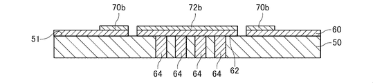
- the second base 50 has, for example, a plate shape.
- the second base 50 is a mounting substrate for mounting the light emitting element 1.
- the first wiring 60 electrically connected to the first electrode 30 and the second electrode electrically connected to the second electrode 40.
- a wiring 62 is provided.
- the second substrate 50 is provided with a through electrode 64 that penetrates the second substrate 50.
- the through electrode 64 is electrically connected to the second electrode 40 via the second wiring 62.
- the second substrate 50 for example, a semiconductor substrate such as a SiC substrate, a ceramic substrate such as an AlN substrate, or the like is used. Semiconductor materials such as SiC and ceramic materials such as AlN have high thermal conductivity and high electrical insulation. Therefore, by using these substrates as the second base 50, the heat dissipation of the light emitting unit 2 can be improved, and the first wiring 60, the second wiring 62, and the through electrode 64 can be easily insulated.
- a metal substrate such as a CuW substrate or a CuMo substrate may be used as the second substrate 50. In this case, when forming the first wiring 60, the second wiring 62, and the through electrode 64, it is necessary to provide an insulating layer or the like between the second base 50 and the wirings 60, 62 and the through electrode 64.
- the thermal expansion coefficient of the second base 50 is preferably close to the thermal expansion coefficient of the first base 10. Thereby, the curvature of the 1st base
- the thermal conductivity of the second substrate 50 is preferably higher than the thermal conductivity of the stacked body 20, for example, and more preferably higher than the thermal conductivity of the first substrate 10.
- the heat capacity of the second base 50 is preferably larger than the heat capacity of the first base 10. Thereby, the heat dissipation of the light emission part 2 (laminated body 20) can be improved.
- the method for measuring the thermal conductivity of the first base 10, the laminate 20, and the second base 50 is not particularly limited.
- the thermal conductivity of the first substrate 10, the laminate 20, and the second substrate 50 may be obtained by, for example, a steady method, or the specific heat capacity and thermal diffusivity obtained by an unsteady method such as a flash method. It may be obtained from Further, when the measurement object is a ceramic substrate or the like, the thermal conductivity may be measured according to JIS R1611.
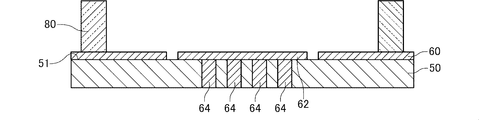
- the first wiring 60 is provided on the main surface 51 of the second base body 50.
- the first wiring 60 is provided in a region overlapping the first electrode 30 in plan view.
- the first wiring 60 is a wiring for electrically connecting the first electrode 30 and an external power supply device (not shown).
- the second wiring 62 is provided on the main surface 51 of the second base 50.
- the second wiring 62 is provided in a region overlapping the second electrode 40 in plan view.
- the second wiring 62 is electrically connected to the through electrode 64.
- the penetrating electrode 64 penetrates the second substrate 50.
- the through electrode 64 is provided in a region overlapping the second wiring 62 in plan view. In the illustrated example, a plurality of through electrodes 64 are provided. The number of through electrodes 64 is not particularly limited.
- the second wiring 62 and the through electrode 64 are wirings for electrically connecting the second electrode 40 and an external power supply device. Power can be supplied to the stacked body 20 (light emitting unit 2) hermetically sealed by the through electrode 64.
- the joining member 70 electrically and mechanically connects the first electrode 30 and the first wiring 60.
- the joining member 70 connects the first electrode 30 and the first wiring 60 so as to ensure airtightness of the space in which the stacked body 20 is accommodated.
- the joining member 72 electrically and mechanically connects the second electrode 40 and the second wiring 62.
- the joining member 70 and the joining member 72 are, for example, Au solder such as AuSn.
- the light emitting device 100 has the following features, for example.
- the stacked body 20 including the light emitting unit 2 is connected to the second base 50 on the side opposite to the first base 10. That is, in the light emitting device 100, the light emitting element 1 is mounted on the second base body 50 in a junction down manner. Thereby, the heat dissipation of the light emission part 2 can be improved. In addition, since the first electrode 30 is connected to the second base body 50, the heat dissipation of the light emitting element 1 can be enhanced.
- the first electrode 30 has one end connected to the first base 10 and the other end connected to the second base 50. Therefore, in the light emitting device 100, the force applied when the light emitting element 1 is mounted on the second substrate 50 in the manufacturing process is distributed to the stacked body 20 and the first electrode 30. Therefore, in the light emitting device 100, it is possible to reduce the pressure applied to the stacked body 20 (light emitting unit 2) during mounting. As a result, it is possible to reduce the possibility of stress and distortion occurring in the light emitting unit 2 (laminated body 20), and to realize a highly reliable light emitting device having stable light emitting characteristics.
- the first electrode 30 that is electrically connected to the first semiconductor layer 22 and has electrical conductivity functions as a member (first member) for reducing the pressure applied to the light emitting unit 2 during mounting. Therefore, in the light emitting device 100, the pressure applied to the light emitting unit 2 during mounting can be reduced without increasing the number of components.
- the first electrode 30 is provided so as to surround the periphery of the stacked body 20. Therefore, in the light-emitting device 100, it can prevent that the force applied at the time of mounting concentrates on the laminated body 20, and can reduce the pressure added to the light emission part 2 at the time of mounting. For example, when the first electrode 30 does not surround the stack 20, the force applied at the time of mounting may be concentrated on the stack 20 rather than the first electrode 30. On the other hand, in the light emitting device 100, since the first electrode 30 surrounds the periphery of the stacked body 20, it is possible to prevent the force applied at the time of mounting from being concentrated on the stacked body 20.
- the stacked body 20 is hermetically sealed by the first electrode 30, the first base 10, and the second base 50. Therefore, in the light emitting device 100, the size of the device can be reduced, the manufacturing process can be simplified, and the cost can be reduced.
- the light emitting element 1 when the light emitting element 1 is sealed with resin or the like, sufficient airtightness cannot be ensured. Further, when the light emitting element 1 is accommodated in a ceramic package using a glass lid, a CAN package, or the like, airtightness can be secured, but there are problems such as an increase in size of the apparatus and cost.
- the stacked body 20 can be hermetically sealed by providing the first electrode 30 so as to surround the stacked body 20, the device can be downsized and the manufacturing process can be simplified. be able to.
- the second substrate 50 is provided with a through electrode 64.
- the second semiconductor layer 26 is electrically connected to the through electrode 64. Therefore, in the light emitting device 100, the second semiconductor layer 26 hermetically sealed by the first electrode 30, the first base 10, and the second base 50 and the external power supply device (not shown) are electrically connected. Can be connected to.
- the first electrode 30 is connected to the second base body 50 via the bonding member 70. Therefore, in the light emitting device 100, the first electrode 30 and the second base body 50 can be more reliably connected.
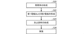
- FIG. 3 is a flowchart showing an example of a method for manufacturing the light emitting device 100 according to the first embodiment.
- 4 to 8 are diagrams schematically showing a manufacturing process of the light emitting device 100 according to the first embodiment.
- 5 is a cross-sectional view taken along line VV in FIG. 6, and
- FIG. 7 is a cross-sectional view taken along line VII-VII in FIG.
- a stacked body 20 including the light emitting unit 2 is formed on the main surface 11 of the first base 10.
- the first semiconductor layer 22, the light emitting layer 24, and the second semiconductor layer 26 are epitaxially grown in this order on the main surface 11 of the first base 10.
- the epitaxial growth method include a MOCVD (Metal Organic Chemical Deposition) method, an MBE (Molecular Beam Epitaxy) method, and the like.
- the first semiconductor layer 22, the light emitting layer 24, and the second semiconductor layer 26 are epitaxially grown in this order on the buffer layer. You may let them.
- the second semiconductor layer 26, the light emitting layer 24, and the first semiconductor layer 22 are patterned.
- the patterning is performed by, for example, photolithography and etching.
- a region 12 where the first base 10 is exposed is formed on the main surface 11 of the first base 10 so as to surround the periphery of the stacked body 20 in plan view.
- a region 23 where the first semiconductor layer 22 is exposed is formed so as to surround the light emitting layer 24 and the second semiconductor layer 26 in plan view.
- the laminated body 20 can be formed by the above process.
- first electrode 30 is formed on the first substrate 10 (region 12) and the first semiconductor layer 22 (region 23), and on the stacked body 20 (on the second semiconductor layer 26). ) To form the second electrode 40.
- the first electrode 30 and the second electrode 40 are formed by, for example, a vacuum deposition method, a lift-off method, or the like.
- the 1st electrode 30 is formed so that the circumference
- the first electrode 30 and the second electrode 30 are set so that the height H30 of the first electrode 30 is equal to the height (H20 + H40) obtained by adding the height H40 of the second electrode 40 to the height H20 of the stacked body 20.
- An electrode 40 is formed. Accordingly, the first electrode 30 and the second base 50 (first wiring 60), and the second electrode 40 and the second base 50 (second wiring 62) can be reliably connected in a mounting step (S14) described later. it can.
- the light-emitting element 1 can be formed.
- the formation order of the 1st electrode 30 and the 2nd electrode 40 is not specifically limited.
- the stacked body 20 is mounted so that the side opposite to the first base 10 is connected to the second base 50 (junction down mounting).
- first electrode 30 and the first wiring 60 are connected by the bonding member 70, and the second electrode 40 and the second wiring 62 are connected by the bonding member 72.
- a first wiring 60, a second wiring 62, and a through electrode 64 are formed on the second base 50 in advance.
- the joining member 70 and the joining member 72 are solders, and the first electrode 30 and the first wiring 60, and the second electrode 40 and the second wiring 62 are soldered, respectively.
- the first electrode 30 is in contact with the joining member 70
- the second electrode 40 is in the joining member 72.
- Heating is performed in a state where the light emitting element 1 is disposed on the second substrate 50 so as to be in contact with the substrate. Accordingly, the first electrode 30 and the first wiring 60 are connected (bonded), and the second electrode 40 and the second wiring 62 are connected (bonded).
- the space for accommodating the stacked body 20 can be made an inert gas atmosphere.
- the laminate 20 formed on the first substrate 10 is pressed against the second substrate 50, so that pressure is applied to the laminate 20.
- the first electrode 30 is formed on the first base 10 in addition to the stacked body 20, the force applied at the time of mounting is distributed to the stacked body 20 and the first electrode 30, and the stacked body The pressure applied to 20 (light emitting unit 2) can be reduced.
- the light emitting element 1 is mounted on the second base 50 and the stacked body 20 is hermetically sealed by the first electrode 30, the first base 10, and the second base 50.
- the light emitting device 100 can be manufactured through the above steps.
- the manufacturing method of the light emitting device 100 according to the present embodiment has the following features, for example.
- the step of forming the stacked body 20 including the light emitting unit 2 on the first base 10 the step of forming the first electrode 30 on the first base 10, Connecting the laminate 20 and the first electrode 30 formed on the base body 10 to the second base body 50 (mounting process). Therefore, as described above, the pressure applied to the stacked body 20 (light emitting unit 2) can be reduced in the mounting process. Therefore, it is possible to reduce the possibility of stress and distortion occurring in the light emitting unit 2 (laminated body 20), and it is possible to manufacture a highly reliable light emitting device having stable light emitting characteristics.
- the first electrode 30 is formed so as to surround the periphery of the multilayer body 20. Therefore, the stacked body 20 can be hermetically sealed by the first electrode 30, the first base 10, and the second base 50 in the mounting process. Therefore, the manufacturing process can be simplified as compared with the case where the light emitting element 1 is hermetically sealed using a ceramic package or a CAN package.
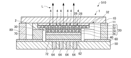
- FIG. 9 is a cross-sectional view schematically showing a light emitting device 110 according to a modification of the first embodiment.
- the planar shape of the light emitting device 110 according to the modification of the first embodiment is the same as the planar shape of the light emitting device 100 shown in FIG.
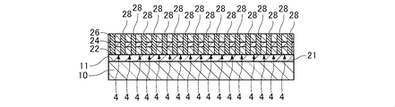
- the light emitting device 110 is different from the light emitting device 100 described above in that the stacked body 20 includes a plurality of columnar portions 4 and the light emitting portion 2 includes a plurality of columnar portions 4.
- the light emitting element 1 is, for example, a semiconductor laser to which a nanostructure is applied.
- the laminate 20 has a buffer layer 21.
- the buffer layer 21 is provided on the main surface 11 of the first base 10.
- the buffer layer 21 is provided between the first semiconductor layer 22 and the first base 10.
- the buffer layer 21 is, for example, an undoped GaN layer.
- the columnar part 4 is provided in the buffer layer 21.
- a plurality of columnar portions 4 are provided.
- the cross-sectional shape of the columnar part 4 (cross-sectional shape in a direction orthogonal to the stacking direction) is, for example, a circle, a polygon (for example, a hexagon), or the like.
- the diameter of the columnar part 4 (inscribed circle diameter in the case of a polygon) is, for example, on the order of nm, and specifically 10 nm or more and 500 nm or less.
- the columnar part 4 is also called, for example, a nanocolumn, nanowire, nanorod, or nanopillar.
- the size of the columnar portions 4 in the stacking direction is, for example, not less than 0.1 ⁇ m and not more than 5 ⁇ m.
- the plurality of columnar portions 4 are separated from each other.
- the interval between the adjacent columnar portions 4 is, for example, not less than 1 nm and not more than 500 nm.
- the columnar portion 4 includes a first semiconductor layer 22, a light emitting layer 24, and a second semiconductor layer 26.
- the plurality of columnar portions 4 are arranged at a predetermined pitch in a predetermined direction in plan view.
- the light generated in the light emitting layer 24 propagates in the direction orthogonal to the stacking direction by the semiconductor layers 22 and 26, and forms a standing wave in the direction orthogonal to the stacking direction in the columnar part 4.
- the layer 24 receives the gain and oscillates. Then, the + 1st order diffracted light and the ⁇ 1st order diffracted light (light L) travel in the stacking direction and are transmitted through the first base 10 and emitted.
- connecting members 28 connected to each of the adjacent columnar portions 4 are provided between the adjacent columnar portions 4.
- the connecting member 28 is continuous between the adjacent columnar parts 4.
- the connection member 28 is a buried layer that is buried between adjacent columnar portions 4. In the illustrated example, the entire space between the adjacent columnar portions 4 is embedded with the connection member 28.
- the connection member 28 connects the adjacent columnar portions 4 or the connection member 28 is connected to each of the adjacent columnar portions 4. This is an expression including a state in which the connection member 28 is embedded.
- connection member 28 between the adjacent columnar portions 4 By providing the connection member 28 between the adjacent columnar portions 4, the strength of the columnar portions 4 can be improved. Therefore, when the light emitting element 1 is mounted on the second base body 50, stress or strain is generated in the columnar portion 4 due to the pressure applied to the columnar portion 4, and defects or dislocations are generated in the columnar portion 4, resulting in unstable light emission characteristics. It is possible to reduce the possibility that the columnar part 4 will be destroyed. Further, even after mounting, when the environmental temperature changes, the stress generated in the columnar portion 4 due to the difference in the thermal expansion coefficient, that is, the second base 50, the first electrode 30, the second electrode 40, which occurs due to the environmental temperature change, for example.
- connection member 28 may include a gap.
- the connection member 28 is provided in the entire space between the adjacent columnar portions 4, but the connection member 28 is provided in a part of the space between the adjacent columnar portions 4. Also good. That is, it is only necessary that a part of the space between the adjacent columnar portions 4 is embedded with the connection member 28. Even in such a case, the strength of the columnar portion 4 can be improved as compared with the case where the connection member 28 is not provided (when the gap between adjacent columnar portions 4 is a gap).
- the connection member 28 is transparent to the light generated in the light emitting layer 24 and can propagate the light generated in the light emitting layer 24.
- the refractive index of the connection member 28 is closer to the refractive index of the light emitting layer 24 than the refractive index of air (gap), for example. That is, the difference between the refractive index of the light emitting layer 24 and the refractive index of the connection member 28 is smaller than the difference between the refractive index of the connection member 28 and the refractive index of air.
- the refractive index of the connection member 28 is lower than the refractive indexes of the semiconductor layers 22 and 26 and the light emitting layer 24, for example.
- the connecting member 28 is made of, for example, an insulating material.
- the material of the connecting member 28 is, for example, GaN, InGaN, TiO2, SiO2, or SiON. Further, polyimide may be used as the connection member 28.
- the connecting member 28 may be composed of a plurality of layers. For example, a portion of the connecting member 28 that contacts the columnar portion 4 is an insulating layer, and a portion that is not in contact with the columnar portion 4 (a region insulated from the columnar portion 4 by the insulating layer) is a conductive layer or a semiconductor made of p-type GaN or the like. It is good also as a layer.
- the light emitting element 1 was a semiconductor laser using a nanostructure
- the light emitting element 1 is a superluminescent diode using a nanostructure or an LED using a nanostructure. It may be.
- the light emitting device 110 can obtain the same effects as the light emitting device 100 described above.
- the stacked body 20 has a plurality of columnar parts 4, and the light emitting part 2 is composed of a plurality of columnar parts 4. Therefore, in the light emitting device 110, dislocations and defects generated in the light emitting layer 24 and the semiconductor layers 22 and 26 can be reduced, and high quality crystals can be obtained. Therefore, the light emitting device 110 can have excellent light emission characteristics.
- 10 to 12 are cross-sectional views schematically showing manufacturing steps of the light emitting device 110 according to the modification of the first embodiment.
- the manufacturing method of the light emitting device 110 is the same as the manufacturing method of the light emitting device 100 shown in FIG. 3, the step of forming the stacked body 20 (S10), and the step of forming the first electrode 30 and the second electrode 40 (S12). And a mounting step (S14).
- the buffer layer 21 is epitaxially grown on the main surface 11 of the first base 10.
- a mask layer (not shown) is formed on the buffer layer 21.
- the mask layer is, for example, a silicon oxide layer, a silicon oxynitride layer, an aluminum oxide layer, a hafnium oxide layer, a titanium layer, a titanium oxide layer, a zirconium oxide layer, a silicon nitride layer, or a laminated film thereof.
- the mask layer is formed by, for example, film formation by sputtering or vapor deposition, and patterning by photolithography and etching.
- the first semiconductor layer 22, the light emitting layer 24, and the second semiconductor layer 26 are epitaxially grown in this order on the buffer layer 21 by MOCVD, MBE, or the like. Thereby, the some columnar part 4 can be formed.
- the connecting member 28 is formed between the adjacent columnar parts 4.
- the connecting member 28 is embedded between the adjacent columnar portions 4.
- the connecting member 28 is SOG (Spin on Glass), polyimide, or the like
- the connecting member 28 is formed by a spin coating method or the like
- the connecting member 28 is an oxide such as TiO 2
- the connecting member 28 is ALD (Atomic Layer). (Deposition) method or the like.
- the connection member 28 is a semiconductor layer such as GaN or InGaN
- the connection member 28 is formed by MOCVD or the like.
- the columnar section 4, the buffer layer 21, and the connecting member 28 are patterned. At this time, a region 12 where the first base 10 is exposed is formed on the main surface 11 of the first base 10. Further, the first semiconductor layer 22 is formed with a region 23 where the first semiconductor layer 22 is exposed.
- the laminated body 20 can be formed by the above process.
- first electrode 30 is formed on the first base 10 (region 12) and the first semiconductor layer 22 (region 23), and on the stacked body 20 (on the second semiconductor layer 26).
- second electrode 40 is formed in the same manner as the step (S12) of forming the first electrode 30 and the second electrode 40 in the method for manufacturing the light emitting device 100 described above. Through the above steps, the light-emitting element 1 can be formed.
- the light emitting device 110 can be manufactured.
- the method for manufacturing the light emitting device 110 according to the present embodiment can achieve the same effects as the method for manufacturing the light emitting device 100 described above.
- FIG. 13 is a cross-sectional view schematically showing the light emitting device 200 according to the second embodiment. Note that the planar shape of the light emitting device 200 according to the second embodiment is the same as the planar shape of the light emitting device 100 shown in FIG.
- the joining member 70 and the joining member 72 shown in FIG. 1 were solder.
- the joining member 70 and the joining member 72 are conductive pastes.
- the conductive paste used as the joining member 70 and the joining member 72 is, for example, a silver paste.
- the silver paste is a paste containing nano-sized silver particles. Note that as the bonding member 70 and the bonding member 72, a paste containing metal particles other than silver particles may be used.
- the height H30 of the first electrode 30 is equal to the height (H20 + H40) obtained by adding the height H20 of the second electrode 40 to the height H20 of the stacked body 20.
- the height H30 of the first electrode 30 is not particularly limited. In the illustrated example, the height H30 of the first electrode 30 is smaller than the height (H20 + H40) obtained by adding the height H40 of the second electrode 40 to the height H20 of the stacked body 20.
- the light emitting device 200 can achieve the same effects as the light emitting device 100 described above.
- 14 to 16 are cross-sectional views schematically showing manufacturing steps of the light emitting device 200 according to the second embodiment.
- the manufacturing method of the light emitting device 200 is the same as the manufacturing method of the light emitting device 100 shown in FIG. 3, the step of forming the stacked body 20 (S10), and the step of forming the first electrode 30 and the second electrode 40 (S12). And a mounting step (S14).
- the stacked body 20 including the light emitting unit 2 is formed on the main surface 11 of the first base 10. This step is performed in the same manner as the step (S10) of forming the stacked body 20 in the method for manufacturing the light emitting device 100 described above.
- first electrode 30 is formed on the first base 10 (region 12) and the first semiconductor layer 22 (region 23), and on the stacked body 20 (on the second semiconductor layer 26). ) To form the second electrode 40.
- the height H30 of the first electrode 30 is smaller than the height (H20 + H40) formed by adding the height H20 of the second electrode 40 to the height H20 of the stacked body 20 except for the above point.
- This is performed in the same manner as the step (S12) of forming the first electrode 30 and the second electrode 40 in the method for manufacturing the light emitting device 100.
- the light-emitting element 1 can be formed.
- the stacked body 20 is mounted so that the side opposite to the first base 10 is connected to the second base 50 (junction down).
- a conductive paste is screen-printed on the first electrode 30 and the second electrode 40 and then baked to form bumps 70a and bumps 72a.
- the bump 70a and the bump 72a are cut out by grinding or cutting to flatten the surface, and the height of the bump 70a and the height of the stacked body 20 plus the height of the second electrode 40 and the bump 72a are obtained. , Make them equal. Accordingly, the first electrode 30 and the second base 50 (first wiring 60), and the second electrode 40 and the second base 50 (second wiring 62) can be reliably connected (joined).
- the first wiring 60, the second wiring 62, and the through electrode 64 are formed on the main surface 51 of the second base 50.
- the conductive paste 70 b and the conductive paste 72 b are screen-printed or applied on the first wiring 60 and the second wiring 62.
- the bump 70a is positioned on the first wiring 60 via the conductive paste 70b
- the bump 72a is positioned on the second wiring 62 via the conductive paste 72b.
- the conductive pastes 70b and 72b are baked. Accordingly, the first electrode 30 and the first wiring 60 are connected (bonded) by the bonding member 70, and the second electrode 40 and the second wiring 62 are connected (bonded) by the bonding member 72.
- the bump 70 a and the conductive paste 70 b form the bonding member 70
- the bump 72 a and the conductive paste 72 b form the bonding member 72.
- the force applied when the light emitting element 1 is mounted on the second substrate 50 is distributed to the stacked body 20 and the first electrode 30, so that the pressure applied to the stacked body 20 (light emitting unit 2) during mounting. Can be reduced.
- the light emitting element 1 is mounted on the second base 50 and the stacked body 20 is hermetically sealed by the first electrode 30, the first base 10, and the second base 50.
- the light emitting device 200 can be manufactured through the above steps.
- the method for manufacturing the light emitting device 200 according to the present embodiment can achieve the same effects as the method for manufacturing the light emitting device 100 described above.
- FIG. 17 is a cross-sectional view schematically showing a light emitting device 210 according to a modification of the second embodiment.
- the planar shape of the light emitting device 210 according to the modification of the second embodiment is the same as the planar shape of the light emitting device 100 shown in FIG.
- the stacked body 20 has a plurality of columnar portions 4, and the light emitting portion 2 is different from the above-described light emitting device 200 in that the light emitting portion 2 is configured by a plurality of columnar portions 4.
- the light emitting element 1 is, for example, a semiconductor laser to which a nanostructure is applied.
- the configuration of the stacked body 20 is the same as the configuration of the stacked body 20 (see FIG. 9) of the light emitting device 110 described above.
- the light emitting device 210 can achieve the same effects as the light emitting device 200 described above. Further, the light emitting device 210 can have excellent light emission characteristics, similar to the light emitting device 110 described above.
- the manufacturing method of the light emitting device 210 is the same as the manufacturing method of the light emitting device 100 shown in FIG. 3, the step of forming the stacked body 20 (S10) and the step of forming the first electrode 30 and the second electrode 40 (S12). And a mounting step (S14).
- the process (S10) of forming the laminated body 20 is performed similarly to the process (S10) of forming the laminated body 20 in the method for manufacturing the light emitting device 110 described above.
- the step (S12) and the mounting step (S14) of forming the first electrode 30 and the second electrode 40 include the step of forming the first electrode 30 and the second electrode 40 in the method for manufacturing the light emitting device 200 described above (S12). ) And the mounting step (S14).
- the method for manufacturing the light emitting device 210 according to the present modification can achieve the same effects as the method for manufacturing the light emitting device 200 described above.
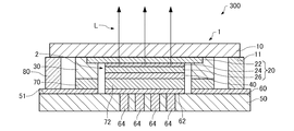
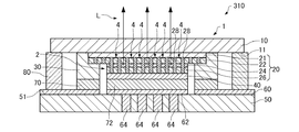
- FIG. 18 is a cross-sectional view schematically showing a light emitting device 300 according to the third embodiment.
- FIG. 19 is a plan view schematically showing the light emitting device 300 according to the third embodiment.
- 18 is a cross-sectional view taken along line XVIII-XVIII in FIG.
- the light-emitting device 300 is provided between the first base 10 and the second base 50, and includes a sealing member 80 ( It differs from the light-emitting device 100 mentioned above by the point comprised including the 2nd member.
- the sealing member 80 has one end connected to the first base 10 and the other end connected to the second base 50.
- the sealing member 80 and the first base 10 are connected to the first base 10 by joining the sealing member 80 directly.
- the sealing member 80 and the second base body 50 are connected by joining the sealing member 80 to the first wiring 60 provided on the second base body 50.
- the sealing member 80 is, for example, low melting point glass.
- the sealing member 80 surrounds the first electrode 30 and the stacked body 20 in a plan view.
- a space for accommodating the first electrode 30 and the stacked body 20 in an airtight manner is formed by the two base bodies 50. That is, the first electrode 30 and the stacked body 20 are hermetically sealed by the sealing member 80, the first base 10, and the second base 50.
- the laminate 20 is surrounded by the first electrode 30, and the first electrode 30 is surrounded by the sealing member 80. That is, the stacked body 20 is doubly surrounded by the first electrode 30 and the sealing member 80 and is double-sealed. Therefore, in the light emitting device 300, the airtightness of the space in which the stacked body 20 is accommodated can be further increased.
- the light emitting device 300 can achieve the same effects as the light emitting device 100 described above.
- the sealing member 80 is provided between the first base 10 and the second base 50, one end of the sealing member 80 is connected to the first base 10, and the other end of the sealing member 80 Is connected to the second base 50. Therefore, in the light emitting device 300, the force applied when the light emitting element 1 is mounted on the second substrate 50 is dispersed in the stacked body 20, the first electrode 30, and the sealing member 80. Therefore, in the light emitting device 300, it is possible to further reduce the pressure applied to the stacked body 20 (light emitting unit 2) during mounting. As a result, it is possible to reduce the possibility of stress and distortion occurring in the light emitting unit 2 (laminated body 20), and to realize a highly reliable light emitting device having stable light emitting characteristics.
- the sealing member 80 is provided so as to surround the first electrode 30 and the stacked body 20. Therefore, in the light emitting device 300, it is possible to prevent the force applied at the time of mounting from being concentrated on the stacked body 20, and the pressure applied to the light emitting unit 2 at the time of mounting can be reduced.
- the first electrode 30 and the stacked body 20 are hermetically sealed by the sealing member 80, the first base 10, and the second base 50. That is, in the light emitting device 300, the stacked body 20 is double-sealed. Therefore, in the light emitting device 300, the airtightness of the space in which the stacked body 20 is accommodated can be further increased.
- the sealing member 80 for sealing the first electrode 30 and the stacked body 20 functions as a member (second member) for reducing the pressure applied to the light emitting unit 2 during mounting. Therefore, in the light emitting device 300, the pressure applied to the light emitting unit 2 during mounting can be reduced without increasing the number of components.
- FIG. 20 is a flowchart illustrating an example of a method for manufacturing the light emitting device 300 according to the third embodiment.
- FIG. 21 is a cross-sectional view schematically showing a manufacturing process of the light emitting device 300 according to the third embodiment.
- the stacked body 20 including the light emitting unit 2 is formed on the main surface 11 of the first base 10. This step is performed in the same manner as the step (S10) of forming the stacked body 20 in the method for manufacturing the light emitting device 100 described above.
- first electrode 30 is formed on the first substrate 10 (region 12) and the first semiconductor layer 22 (region 23), and the second electrode 40 is formed on the stacked body 20 (on the second semiconductor layer 26).
- This step is performed in the same manner as the step (S12) of forming the first electrode 30 and the second electrode 40 in the method for manufacturing the light emitting device 100 described above. Through the above steps, the light-emitting element 1 can be formed (see FIG. 7).
- a sealing member 80 is formed on the main surface 51 of the second base 50.
- the sealing member 80 is formed by applying glass frit to the main surface 51 of the second substrate 50 and firing the glass frit. In this way, by firing the glass frit in advance, the solvent in the glass frit can be blown off and the solvent remaining in the space sealed by the sealing member 80 can be prevented.
- a first wiring 60, a second wiring 62, and a through electrode 64 are formed on the second base 50 in advance.
- first, the first electrode 30 and the first wiring 60 are connected (solder bonding) by the bonding member 70, and the second electrode 40 and the second wiring 62 are connected by the bonding member 72 (solder bonding). .
- the sealing member 80 is irradiated with laser, one end of the sealing member 80 is fused to the first base 10, and the other end of the sealing member 80 is fused to the second base 50. Thereby, one end of the sealing member 80 is connected (bonded) to the first base 10, and the other end of the sealing member 80 is connected (bonded) to the second base 50.
- the space for accommodating the first electrode 30 and the stacked body 20 can be made an inert gas atmosphere.
- the stacked body 20 formed on the first substrate 10 is pressed against the second substrate 50, so that pressure is applied to the stacked body 20.
- the first electrode 30 is formed on the first base 10
- the sealing member 80 is formed on the second base 50. Therefore, the force applied at the time of mounting is distributed to the stacked body 20, the first electrode 30, and the sealing member 80, and the pressure applied to the stacked body 20 (light emitting unit 2) can be reduced.
- the light-emitting element 1 is mounted on the second base 50 and the first electrode 30 and the stacked body 20 are hermetically sealed by the sealing member 80, the first base 10, and the second base 50.
- connection (bonding) between the first electrode 30 and the first wiring 60, the connection (bonding) between the second electrode 40 and the second wiring 62, and the connection (fusion) between the sealing member 80 and the bases 10 and 50. ) May be performed simultaneously. That is, the joining members 70 and 72 (for example, AuSn solder) and the sealing member 80 (low melting point glass) may be heated at the same time, and the respective connections (joining and fusion) may be performed simultaneously.
- the light emitting device 300 can be manufactured through the above steps.
- the method for manufacturing the light emitting device 300 according to the present embodiment can achieve the same effects as the method for manufacturing the light emitting device 100 described above.
- the pressure applied to the stacked body 20 (light emitting unit 2) by the first electrode 30 and the sealing member 80 in the mounting process can be reduced. Therefore, it is possible to reduce the possibility that stress or distortion occurs in the light emitting unit 2 (laminated body 20), and it is possible to manufacture a highly reliable light emitting device having stable light emitting characteristics.
- the sealing member 80 is formed so as to surround the first electrode 30. Therefore, the stacked body 20 can be double-sealed by the sealing member 80 and the first electrode 30 by performing junction down mounting of the light emitting element 1 on the second base 50. Thereby, the airtightness of the space in which the stacked body 20 is accommodated can be further enhanced.
- FIG. 22 is a cross-sectional view schematically showing a light emitting device 310 according to a modification of the third embodiment.
- the planar shape of the light emitting device 310 according to the modification of the third embodiment is the same as the planar shape of the light emitting device 300 shown in FIG.
- the stacked body 20 has a plurality of columnar portions 4, and the light emitting portion 2 is different from the above-described light emitting device 300 in that it is composed of a plurality of columnar portions 4.
- the light emitting element 1 is, for example, a semiconductor laser to which a nanostructure is applied.
- the configuration of the light-emitting device 310 is the same as that of the light-emitting device 300 except that the light-emitting element 1 is the light-emitting element 1 (see FIG. 9) of the light-emitting device 110 described above.
- the light emitting device 310 can achieve the same effects as the light emitting device 300 described above. Furthermore, the light emitting device 310 can have excellent light emission characteristics, similar to the light emitting device 110 described above.
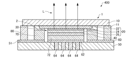
- FIG. 23 is a cross-sectional view schematically showing a light emitting device 400 according to the fourth embodiment.
- the planar shape of the light emitting device 400 according to the fourth embodiment is the same as the planar shape of the light emitting device 300 shown in FIG.
- the light emitting device 400 is provided between the first base 10 and the second base 50, and includes a sealing member 80 (second member) surrounding the first electrode 30 and the stacked body 20. ) Is different from the light-emitting device 200 described above.
- the configuration of the light emitting device 400 is the same as the configuration of the light emitting device 300 (see FIG. 18) except that the configuration of the light emitting element 1 is the same as the configuration of the light emitting element 1 (see FIG. 13) of the light emitting device 200 described above. The description is omitted.
- the light emitting device 400 can achieve the same effects as the light emitting device 300 described above.
- the manufacturing method of the light emitting device 400 according to the fourth embodiment can be manufactured by combining the manufacturing method of the light emitting device 200 according to the second embodiment and the manufacturing method of the light emitting device 300 according to the third embodiment. .
- the manufacturing method of the light emitting device 400 can achieve the same effects as the manufacturing method of the light emitting devices 200 and 300 described above.
- FIG. 24 is a cross-sectional view schematically showing a light emitting device 410 according to a modification of the fourth embodiment.
- the planar shape of the light-emitting device 410 which concerns on the modification of 4th Embodiment is the same as the planar shape of the light-emitting device 300 shown in FIG. 19, and abbreviate
- the stacked body 20 has a plurality of columnar portions 4, and the light emitting portion 2 is different from the above-described light emitting device 400 in that it is composed of a plurality of columnar portions 4.
- the light emitting element 1 is, for example, a semiconductor laser to which a nanostructure is applied.
- the configuration of the light-emitting device 410 is the same as that of the light-emitting device 400 except that the light-emitting element 1 is the light-emitting element 1 (see FIG. 17) of the light-emitting device 210 described above, and a description thereof is omitted.
- the light emitting device 410 can achieve the same effects as the light emitting device 400 described above.
- the light emitting device 410 can have excellent light emission characteristics, similar to the light emitting device 210 described above.
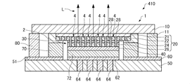
- FIG. 25 is a cross-sectional view schematically showing a light emitting device 500 according to the fifth embodiment.
- FIG. 26 is a plan view schematically showing a light emitting device 500 according to the fifth embodiment.
- FIG. 25 is a sectional view taken along line XXV-XXV in FIG.
- the first electrode 30 includes a space in which the stacked body 20 inside the first electrode 30 is accommodated, and the first electrode 30 and the sealing member 80. It differs from the light emitting device 400 in that a slit portion 32 that communicates with the space between the light emitting devices 400 is provided. That is, in the light emitting device 500, the stacked body 20 is not sealed by the first electrode 30 and is hermetically sealed only by the sealing member 80.
- the first electrode 30 Since the slit portion 32 is formed in the first electrode 30, the first electrode 30 does not surround the laminate 20.
- the first electrode 30 has a shape in which a part of the side wall of the rectangular tube is cut out.
- the pressure applied to the laminated body 20 (light emitting part 2) at the time of mounting can be reduced.
- the light emitting device 500 according to the fifth embodiment can achieve the same effects as the light emitting device 400 described above.
- the manufacturing method of the light emitting device 500 according to the fifth embodiment is that the slit portion 32 is provided in the first electrode 30 and the gas is exhausted through the slit portion 32 in the light emitting device 400 according to the fourth embodiment described above. Different from the manufacturing method. Hereinafter, this difference will be described.
- the slit portion 32 is formed in the first electrode 30 in the step of forming the first electrode 30 and the second electrode 40.
- the space inside the first electrode 30 is exhausted through the slit portion 32 and replaced with an inert gas.
- the first electrode 30 and the first wiring 60 are joined by the joining member 70 (conductive paste), and the second electrode 40 and the second wiring 62 are joined by the joining member 72 (conductive paste). Join.
- gas is generated from the joining members 70 and 72 by baking the conductive paste.
- the gas is exhausted from the space inside the first electrode 30 through the slit portion 32 and replaced with an inert gas.
- the sealing member 80 is irradiated with a laser so that one end of the sealing member 80 is fused to the first base 10 and the other end of the sealing member 80 is fused to the second base 50. Thereby, the stacked body 20 and the first electrode 30 can be hermetically sealed.
- the solvent is vaporized from the conductive paste to generate gas.
- the stack 20 (light emitting unit 2) may be contaminated by this gas.
- the slit portion 32 is not provided in the first electrode 30, the space in which the stacked body 20 is accommodated is hermetically sealed by firing the conductive paste, and gas generated from the conductive paste is sealed in this space. It will remain.
- the gas generated from the conductive paste can be removed by providing the slit portion 32 in the first electrode 30. As a result, contamination of the stacked body 20 by gas can be reduced.
- the method for manufacturing the light emitting device 500 according to the fifth embodiment can achieve the same effects as the method for manufacturing the light emitting device 400 according to the fourth embodiment.
- the gas generated from the joining members 70 and 72 can be removed through the slit portion 32 in the mounting process. Therefore, contamination of the stacked body 20 (light emitting unit 2) due to the gas generated from the joining members 70 and 72 during mounting can be reduced.
- FIG. 27 is a cross-sectional view schematically showing a light emitting device 510 according to a modification of the fifth embodiment.
- the planar shape of the light emitting device 510 according to the modification of the fifth embodiment is the same as the planar shape of the light emitting device 500 shown in FIG.
- the stacked body 20 has a plurality of columnar portions 4, and the light emitting portion 2 is different from the light emitting device 500 described above in that it is composed of a plurality of columnar portions 4.
- the light emitting element 1 is, for example, a semiconductor laser to which a nanostructure is applied.
- the configuration of the light-emitting device 510 is the same as that of the light-emitting device 500 except that the light-emitting element 1 is the light-emitting element 1 (see FIG. 17) of the light-emitting device 210 described above.
- the light emitting device 510 can achieve the same effects as the light emitting device 500 described above. Further, the light emitting device 510 can have excellent light emission characteristics, similar to the light emitting device 210 described above.
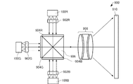
- FIG. 28 is a diagram schematically showing a projector 900 according to the sixth embodiment.
- the projector according to the present invention includes the light emitting device according to the present invention.
- a projector 900 including the light emitting device 100 as the light emitting device according to the present invention will be described.
- the projector 900 includes a housing (not shown), and a red light source 100R, a green light source 100G, and a blue light source 100B that emit red light, green light, and blue light provided in the housing.
- Each of the red light source 100R, the green light source 100G, and the blue light source 100B includes, for example, a plurality of light emitting devices 100 arranged in an array in a direction orthogonal to the stacking direction, and the second substrate 50 is used as a common substrate in the plurality of light emitting devices 100. It is what.
- the number of the light emitting devices 100 constituting each of the light sources 100R, 100G, and 100B is not particularly limited. For the sake of convenience, in FIG. 28, the casing that constitutes the projector 900 is omitted, and the light sources 100R, 100G, and 100B are simplified.
- the projector 900 further includes lens arrays 902R, 902G, and 902B, transmissive liquid crystal light valves (light modulation devices) 904R, 904G, and 904B and a projection lens (projection device) 908 provided in the housing.
- lens arrays 902R, 902G, and 902B transmissive liquid crystal light valves (light modulation devices) 904R, 904G, and 904B and a projection lens (projection device) 908 provided in the housing.
- the light emitted from the light sources 100R, 100G, and 100B is incident on the lens arrays 902R, 902G, and 902B.
- Light emitted from the light sources 100R, 100G, and 100B is collected by the lens arrays 902R, 902G, and 902B, and can be superimposed (partially superimposed), for example.
- the liquid crystal light valves 904R, 904G, and 904B can be irradiated with good uniformity.
- the light condensed by the lens arrays 902R, 902G, and 902B is incident on the liquid crystal light valves 904R, 904G, and 904B.
- Each of the liquid crystal light valves 904R, 904G, and 904B modulates incident light according to image information.
- the projection lens 908 enlarges and projects an image (image) formed by the liquid crystal light valves 904R, 904G, and 904B onto a screen (display surface) 910.
- the projector 900 can include a cross dichroic prism (color light combining means) 906 that combines the light emitted from the liquid crystal light valves 904R, 904G, and 904B and guides the light to the projection lens 908.
- a cross dichroic prism color light combining means
- the three color lights modulated by the liquid crystal light valves 904R, 904G, and 904B are incident on the cross dichroic prism 906.
- This prism is formed by bonding four right-angle prisms, and a dielectric multilayer film that reflects red light and a dielectric multilayer film that reflects blue light are arranged in a cross shape on the inner surface thereof.
- These dielectric multilayer films combine the three color lights to form light representing a color image.
- the synthesized light is projected onto the screen 910 by the projection lens 908 which is a projection optical system, and an enlarged image is displayed.
- the light sources 100R, 100G, and 100B control the liquid crystal light valves 904R, 904G, and 904B by controlling (modulating) the light emitting devices 100 constituting the light sources 100R, 100G, and 100B as image pixels according to image information. You may form an image
- the projection lens 908 may enlarge and project the image formed by the light sources 100R, 100G, and 100B onto the screen 910.
- a transmissive liquid crystal light valve is used as the light modulation device, but a light valve other than liquid crystal may be used, or a reflective light valve may be used. Examples of such a light valve include a reflective liquid crystal light valve and a digital micromirror device (Digital Micromirror Device). Further, the configuration of the projection optical system is appropriately changed depending on the type of light valve used.
- the light source 100R, 100G, 100B has scanning means that is an image forming apparatus that displays an image of a desired size on the display surface by causing the light from the light source 100R, 100G, 100B to scan on the screen.
- the present invention can also be applied to a light source device of a simple scanning image display device (projector).
- the light-emitting element 1 is junction-down mounted by bonding the second electrode 40 to the second base 50 (second wiring 62).
- the body 20 is provided with a member (metal layer or the like) for transferring the heat generated in the light emitting unit 2 to the second base 50, and the light emitting element 1 is junction-down mounted by joining the member to the second base 50. May be.
- the second electrode 40 may not be bonded to the second substrate 50. This modification can also be applied to the second to fifth embodiments described above.
- the first electrode 30 is connected (bonded) to the second base body 50 by the bonding member 70 to hermetically seal the stacked body 20.
- the pressure applied to the laminated body 20 during the mounting was reduced, but it was a member separate from the first electrode 30 and having one end connected to the first base 10 and the other end connected to the second base 50.
- First member may be provided to reduce the pressure applied to the stacked body 20 during mounting.
- the member does not necessarily have to be bonded (adhered) to the second base 50 and may be in contact with the second base 50 as long as the pressure applied to the stacked body 20 at the time of mounting can be reduced.
- the member may be an insulating member. This modification can also be applied to the second to fifth embodiments described above.
- Apps of the light-emitting device according to the present invention are not limited to the above-described embodiments, but besides projectors, indoor / outdoor lighting, display backlights, laser printers, scanners, in-vehicle lights, sensing devices using light, communication It can also be used as a light source for equipment and the like.
- the present invention includes substantially the same configuration (for example, a configuration having the same function, method, and result, or a configuration having the same purpose and effect) as the configuration described in the embodiment.
- the invention includes a configuration in which a non-essential part of the configuration described in the embodiment is replaced.
- the present invention includes a configuration that exhibits the same operational effects as the configuration described in the embodiment or a configuration that can achieve the same object.
- the invention includes a configuration in which a known technique is added to the configuration described in the embodiment.
Abstract
A light emitting device is provided which enables reducing the pressure applied to a light emitting unit during mounting. This light-emitting device is provided with: a light emitting element which comprises a first base body on which a laminate body is provided; a second base body on which the light-emitting element is provided; the laminate body which is provided on the first base body; and a first member which is provided between the first base body and the second base body. The laminate body includes a light-emitting unit. The light-emitting unit comprises a first semiconductor layer, a second semiconductor layer having a conductivity type different from that of the first semiconductor layer, and a light emitting layer which is provided between the first semiconductor layer and the second semiconductor layer and can emit light through the injection of current. The first member is connected at one end to the first base body and is connected at the other end to the second base body, and the laminate body is connected to the second base body on the side opposite of the first base body.
Description
本発明は、発光装置、プロジェクター、および発光装置の製造方法に関する。
The present invention relates to a light emitting device, a projector, and a method for manufacturing the light emitting device.
半導体レーザーや、発光ダイオードなどの発光素子の実装方法としてジャンクションダウン実装が知られている。発光素子をジャンクションダウン実装することで、発光素子で発生した熱を効率よく放熱できる。
Junction-down mounting is known as a mounting method for light emitting elements such as semiconductor lasers and light emitting diodes. By junction-down mounting the light emitting element, heat generated in the light emitting element can be efficiently dissipated.
例えば特許文献1には、レーザーチップの表面電極をヒートシンクとなるマウントに半田材によって接着してジャンクションダウン実装した発光素子が開示されている。レーザーチップは、基板と、基板上に形成された、下部クラッド層、量子井戸層、および上部クラッド層を含む能動層と、能動層上に形成された表面電極と、基板の裏面に設けられた裏面電極と、で構成されている。
For example, Patent Document 1 discloses a light-emitting element in which a surface electrode of a laser chip is bonded to a mount serving as a heat sink with a solder material and junction-down mounted. The laser chip is provided on the substrate, the active layer formed on the substrate including the lower cladding layer, the quantum well layer, and the upper cladding layer, the surface electrode formed on the active layer, and the back surface of the substrate And a back electrode.
しかしながら、特許文献1の発光素子では、製造工程においてマウントにレーザーチップの表面電極を接合して発光素子をマウントに実装する際に、能動層に大きな圧力が加わり、能動層(発光部)に応力や歪みが生じてしまう。この結果、能動層に欠陥や転位が生じて発光特性が不安定になったり、能動層が破壊されてしまったりする可能性がある。
However, in the light-emitting element of Patent Document 1, when the surface electrode of the laser chip is bonded to the mount and the light-emitting element is mounted on the mount in the manufacturing process, a large pressure is applied to the active layer, and stress is applied to the active layer (light-emitting portion). And distortion will occur. As a result, defects or dislocations may occur in the active layer, resulting in instability of light emission characteristics or destruction of the active layer.
本発明のいくつかの態様に係る目的の1つは、実装時に発光部に加わる圧力を低減できる発光装置を提供することにある。また、本発明のいくつかの態様に係る目的の1つは、上記発光装置を含むプロジェクターを提供することにある。また、本発明のいくつかの態様に係る目的の1つは、実装時に発光部に加わる圧力を低減できる発光装置の製造方法を提供することにある。
One of the objects according to some aspects of the present invention is to provide a light-emitting device that can reduce the pressure applied to the light-emitting portion during mounting. Another object of some embodiments of the present invention is to provide a projector including the light-emitting device. Another object of some aspects of the present invention is to provide a method for manufacturing a light-emitting device that can reduce the pressure applied to the light-emitting portion during mounting.
本発明に係る発光装置は、
積層体が設けられている第1基体を含む発光素子と、
前記発光素子が設けられている第2基体と、
前記第1基体と前記第2基体との間に設けられている第1部材と、を含み、
前記積層体は、発光部を含み、
前記発光部は、
第1半導体層と、
前記第1半導体層と導電型の異なる第2半導体層と、
前記第1半導体層と前記第2半導体層との間に設けられ、電流が注入されることで光を発することが可能な発光層と、を有し、
前記第1部材は、一端が前記第1基体に接続され、他端が前記第2基体に接続され、
前記積層体は、前記第1基体と反対側において、前記第2基体に接続されている。 The light emitting device according to the present invention is
A light emitting device including a first substrate provided with a laminate;
A second substrate provided with the light emitting element;
A first member provided between the first base and the second base,
The laminate includes a light emitting unit,
The light emitting unit
A first semiconductor layer;
A second semiconductor layer having a conductivity type different from that of the first semiconductor layer;
A light emitting layer provided between the first semiconductor layer and the second semiconductor layer and capable of emitting light when a current is injected;
The first member has one end connected to the first base and the other end connected to the second base.
The laminate is connected to the second base on the side opposite to the first base.
このような発光装置では、一端が第1基体に接続され他端が第2基体に接続されている第1部材を含むため、製造工程において積層体を第2基体に接続する際(すなわち積層体を含む発光素子を第2基体に実装する際)に加えられる力が、積層体と第1部材とに分散される。したがって、このような発光装置では、実装時に、発光部(積層体)に加わる圧力を低減できる。この結果、発光部(積層体)に応力や歪みが生じる可能性を低減でき、安定した発光特性を有する信頼性の高い発光装置を実現できる。
Since such a light emitting device includes a first member having one end connected to the first base and the other end connected to the second base, the stack is connected to the second base in the manufacturing process (that is, the stack). The force applied to the light-emitting element including the light-emitting element when mounted on the second substrate is dispersed in the laminate and the first member. Therefore, in such a light emitting device, it is possible to reduce the pressure applied to the light emitting unit (laminated body) during mounting. As a result, it is possible to reduce the possibility of stress and distortion occurring in the light emitting portion (laminated body), and to realize a highly reliable light emitting device having stable light emitting characteristics.
本発明に係る発光装置において、
前記第1部材は、前記積層体の周囲を囲って設けられていてもよい。 In the light emitting device according to the present invention,
The first member may be provided so as to surround the periphery of the stacked body.
前記第1部材は、前記積層体の周囲を囲って設けられていてもよい。 In the light emitting device according to the present invention,
The first member may be provided so as to surround the periphery of the stacked body.
このような発光装置では、実装時に加えられる力が積層体に集中することを防ぐことができ、実装時に発光部(積層体)に加わる圧力を低減できる。
In such a light emitting device, it is possible to prevent the force applied at the time of mounting from being concentrated on the laminated body, and to reduce the pressure applied to the light emitting part (laminated body) at the time of mounting.
本発明に係る発光装置において、
前記積層体は、前記第1部材、前記第1基体、および前記第2基体によって気密に封止されていてもよい。 In the light emitting device according to the present invention,
The laminate may be hermetically sealed with the first member, the first base, and the second base.
前記積層体は、前記第1部材、前記第1基体、および前記第2基体によって気密に封止されていてもよい。 In the light emitting device according to the present invention,
The laminate may be hermetically sealed with the first member, the first base, and the second base.
このような発光装置では、例えば発光素子をセラミックパッケージやCANパッケージなどのパッケージによって気密に封止する場合と比べて、装置の小型化、製造工程の簡略化を図ることができる。
In such a light emitting device, for example, the device can be reduced in size and the manufacturing process can be simplified as compared with a case where the light emitting element is hermetically sealed with a package such as a ceramic package or a CAN package.
本発明に係る発光装置において、
前記第1部材は導電性を有し、前記第1半導体層に電気的に接続されていてもよい。 In the light emitting device according to the present invention,
The first member may be conductive and electrically connected to the first semiconductor layer.
前記第1部材は導電性を有し、前記第1半導体層に電気的に接続されていてもよい。 In the light emitting device according to the present invention,
The first member may be conductive and electrically connected to the first semiconductor layer.
このような発光装置では、第1部材を第1半導体層に電流を注入する電極としても機能させることができる。
In such a light emitting device, the first member can also function as an electrode for injecting current into the first semiconductor layer.
本発明に係る発光装置において、
前記第1基体と前記第2基体との間に設けられている第2部材を含み、
前記第2部材は、一端が前記第1基体に接続され、他端が前記第2基体に接続されていてもよい。 In the light emitting device according to the present invention,
Including a second member provided between the first base and the second base;
The second member may have one end connected to the first base and the other end connected to the second base.
このような発光装置では、実装時に加えられる力が、積層体と、第1部材と、第2部材と、に分散されるため、実装時に発光部(積層体)に加わる圧力をより低減できる。
In such a light-emitting device, the force applied during mounting is distributed to the stacked body, the first member, and the second member, so that the pressure applied to the light-emitting portion (laminated body) during mounting can be further reduced.
本発明に係る発光装置において、
前記第2部材は、前記第1部材および前記積層体の周囲を囲っていてもよい。 In the light emitting device according to the present invention,
The second member may surround the first member and the laminate.
前記第2部材は、前記第1部材および前記積層体の周囲を囲っていてもよい。 In the light emitting device according to the present invention,
The second member may surround the first member and the laminate.
このような発光装置では、実装時に加えられる力が積層体に集中することを防ぐことができ、実装時に発光部(積層体)に加わる圧力を低減できる。
In such a light emitting device, it is possible to prevent the force applied at the time of mounting from being concentrated on the laminated body, and to reduce the pressure applied to the light emitting part (laminated body) at the time of mounting.
本発明に係る発光装置において、
前記第2基体には、前記第2基体を貫通する貫通電極が設けられていてもよい。 In the light emitting device according to the present invention,
The second substrate may be provided with a penetrating electrode that penetrates the second substrate.
前記第2基体には、前記第2基体を貫通する貫通電極が設けられていてもよい。 In the light emitting device according to the present invention,
The second substrate may be provided with a penetrating electrode that penetrates the second substrate.
このような発光装置では、第1部材、第1基体、および第2基体によって気密に封止された積層体(発光部)と、外部の電源装置と、を電気的に接続することができる。
In such a light-emitting device, the laminate (light-emitting portion) hermetically sealed by the first member, the first base, and the second base can be electrically connected to the external power supply device.
本発明に係る発光装置において、
前記第2半導体層は、前記貫通電極に電気的に接続されていてもよい。 In the light emitting device according to the present invention,
The second semiconductor layer may be electrically connected to the through electrode.
前記第2半導体層は、前記貫通電極に電気的に接続されていてもよい。 In the light emitting device according to the present invention,
The second semiconductor layer may be electrically connected to the through electrode.
このような発光装置では、第1部材、第1基体、および第2基体によって気密に封止された積層体(発光部)に含まれる第2半導体層と、外部の電源装置と、を電気的に接続することができる。
In such a light emitting device, the first member, the first base, and the second semiconductor layer included in the stacked body (light emitting portion) hermetically sealed by the second base are electrically connected to the external power supply device. Can be connected to.
本発明に係る発光装置において、
前記積層体は、複数の柱状部を有し、
前記発光部は、前記複数の柱状部で構成されていてもよい。 In the light emitting device according to the present invention,
The laminate has a plurality of columnar parts,
The light emitting unit may be composed of the plurality of columnar parts.
前記積層体は、複数の柱状部を有し、
前記発光部は、前記複数の柱状部で構成されていてもよい。 In the light emitting device according to the present invention,
The laminate has a plurality of columnar parts,
The light emitting unit may be composed of the plurality of columnar parts.
このような発光装置では、第1半導体層、発光層、および第2半導体層に発生する転位や欠陥を低減することができ、高い品質の結晶を得ることができる。したがって、このような発光装置では、優れた発光特性を有することができる。
In such a light emitting device, dislocations and defects generated in the first semiconductor layer, the light emitting layer, and the second semiconductor layer can be reduced, and high quality crystals can be obtained. Therefore, such a light emitting device can have excellent light emission characteristics.
本発明に係る発光装置において、
前記第1部材は、接合部材を介して前記第2基体に接続されていてもよい。 In the light emitting device according to the present invention,
The first member may be connected to the second base via a bonding member.
前記第1部材は、接合部材を介して前記第2基体に接続されていてもよい。 In the light emitting device according to the present invention,
The first member may be connected to the second base via a bonding member.
このような発光装置では、第1部材を第2基体に確実に接続(接合)することができる。
In such a light emitting device, the first member can be reliably connected (joined) to the second base.
本発明に係るプロジェクターは、本発明に係る発光装置を含む。
The projector according to the present invention includes the light emitting device according to the present invention.
このようなプロジェクターでは、本発明に係る発光装置を含むことができる。
Such a projector can include the light emitting device according to the present invention.
本発明に係る発光装置の製造方法は、
第1基体に、発光部を含む積層体を形成する工程と、
前記第1基体に、第1部材を形成する工程と、
前記第1基体に形成された前記積層体および前記第1部材を、第2基体に接続する工程と、を含み、
前記発光部は、
第1半導体層と、
前記第1半導体層と導電型の異なる第2半導体層と、
前記第1半導体層と前記第2半導体層との間に設けられ、電流が注入されることで光を発することが可能な発光層と、を有している。 A method for manufacturing a light emitting device according to the present invention includes:
Forming a laminate including a light emitting portion on the first substrate;
Forming a first member on the first base;
Connecting the laminate formed on the first base and the first member to a second base, and
The light emitting unit
A first semiconductor layer;
A second semiconductor layer having a conductivity type different from that of the first semiconductor layer;
A light emitting layer provided between the first semiconductor layer and the second semiconductor layer and capable of emitting light when a current is injected.
このような発光装置の製造方法では、積層体および第1部材を第2基体に接続する工程(実装工程)において、実装時(積層体を第2基体に接続する際)に加えられる力が積層体と第1部材とに分散される。したがって、実装時に、発光部(積層体)に加わる圧力を低減できる。この結果、発光部(積層体)に応力や歪みが生じる可能性を低減でき、安定した発光特性を有する信頼性の高い発光装置を製造できる。
In such a method for manufacturing a light emitting device, in the step of connecting the laminate and the first member to the second substrate (mounting step), the force applied during mounting (when the laminate is connected to the second substrate) is laminated. Dispersed in the body and the first member. Therefore, the pressure applied to the light emitting part (laminated body) at the time of mounting can be reduced. As a result, the possibility of stress and distortion occurring in the light emitting portion (laminated body) can be reduced, and a highly reliable light emitting device having stable light emitting characteristics can be manufactured.
以下、本発明の好適な実施形態について図面を用いて詳細に説明する。なお、以下に説明する実施形態は、特許請求の範囲に記載された本発明の内容を不当に限定するものではない。また、以下で説明される構成の全てが本発明の必須構成要件であるとは限らない。
Hereinafter, preferred embodiments of the present invention will be described in detail with reference to the drawings. The embodiments described below do not unduly limit the contents of the present invention described in the claims. In addition, not all of the configurations described below are essential constituent requirements of the present invention.
1. 第1実施形態
1.1. 発光装置
まず、第1実施形態に係る発光装置について図面を参照しながら説明する。図1は、第1実施形態に係る発光装置100を模式的に示す断面図である。図2は、第1実施形態に係る発光装置100を模式的に示す平面図である。なお、図1は、図2のI-I線断面図である。 1. 1. First embodiment 1.1. First, the light emitting device according to the first embodiment will be described with reference to the drawings. FIG. 1 is a cross-sectional view schematically showing alight emitting device 100 according to the first embodiment. FIG. 2 is a plan view schematically showing the light emitting device 100 according to the first embodiment. 1 is a cross-sectional view taken along the line II of FIG.
1.1. 発光装置
まず、第1実施形態に係る発光装置について図面を参照しながら説明する。図1は、第1実施形態に係る発光装置100を模式的に示す断面図である。図2は、第1実施形態に係る発光装置100を模式的に示す平面図である。なお、図1は、図2のI-I線断面図である。 1. 1. First embodiment 1.1. First, the light emitting device according to the first embodiment will be described with reference to the drawings. FIG. 1 is a cross-sectional view schematically showing a
発光装置100は、図1に示すように、第1基体10、積層体20、第1電極30(第1部材)、および第2電極40を有する発光素子1と、第2基体50と、を含む。
As shown in FIG. 1, the light emitting device 100 includes a light emitting element 1 having a first base 10, a laminate 20, a first electrode 30 (first member), and a second electrode 40, and a second base 50. Including.
発光装置100では、第1基体10、積層体20、第1電極30、および第2電極40が発光素子1を構成し、発光素子1が第2基体50(実装基板)にジャンクションダウン実装されている。
In the light emitting device 100, the first base 10, the stacked body 20, the first electrode 30, and the second electrode 40 constitute the light emitting element 1, and the light emitting element 1 is junction-down mounted on the second base 50 (mounting substrate). Yes.
第1基体10は、例えば、板状の形状を有している。第1基体10は、例えば、サファイア基板である。第1基体10は、発光層24で発生した光Lに対して透明である。そのため、発光層24で発生した光Lは、第1基体10を透過して外部に出射される。すなわち、発光装置100は、第1基体10側から光Lを出射する。なお、第1基体10は、サファイア基板に限定されず、その他のセラミックス基板やガラス基板などを用いることができる。
The first base 10 has, for example, a plate shape. The first base 10 is, for example, a sapphire substrate. The first substrate 10 is transparent to the light L generated in the light emitting layer 24. Therefore, the light L generated in the light emitting layer 24 passes through the first base 10 and is emitted to the outside. That is, the light emitting device 100 emits light L from the first base 10 side. In addition, the 1st base | substrate 10 is not limited to a sapphire substrate, Other ceramic substrates, a glass substrate, etc. can be used.
積層体20は、第1基体10に設けられている。積層体20は、第1基体10の主面11に設けられている。積層体20は、第1基体10と第2基体50との間に位置している。積層体20は、第1基体10の主面11に積層された複数の層で構成されている。積層体20は、発光部2を含む。発光部2は、第1半導体層22と、発光層24と、第2半導体層26と、を有している。
The laminate 20 is provided on the first base 10. The stacked body 20 is provided on the main surface 11 of the first base 10. The stacked body 20 is located between the first base 10 and the second base 50. The stacked body 20 is composed of a plurality of layers stacked on the main surface 11 of the first base 10. The stacked body 20 includes the light emitting unit 2. The light emitting unit 2 includes a first semiconductor layer 22, a light emitting layer 24, and a second semiconductor layer 26.
上述したように、発光装置100では、発光素子1は第2基体50にジャンクションダウン実装されている。すなわち、発光装置100では、積層体20が第1基体10の反対側において第2基体50に接続されている。積層体20は、第2電極40および接合部材72を介して、第2基体50(第2配線62)に接続されている。
As described above, in the light emitting device 100, the light emitting element 1 is mounted on the second base 50 in a junction-down manner. That is, in the light emitting device 100, the stacked body 20 is connected to the second base 50 on the opposite side of the first base 10. The stacked body 20 is connected to the second base body 50 (second wiring 62) via the second electrode 40 and the bonding member 72.
なお、本発明に係る記載では、「接続」という文言を、例えば、「特定のもの(以下、「A」という)が他の特定のもの(以下、「B」という)に接続されている」などと用いる場合に、AがBに、直接、接続されているような(AとBが接しているような)場合と、Aが他のものを介してBに接続されているような場合と、が含まれるものとして、「接続」という文言を用いている。また、本発明に係る記載では、「設ける」という文言を、例えば、「特定のもの(以下、「C」という)が他の特定のもの(以下、「D」という)に設けられている」などと用いる場合に、CがDに、直接、設けられているような(CとDが接しているような)場合と、Cが他のものを介してDに設けられているような場合と、が含まれるものとして、「設ける」という文言を用いている。
In the description according to the present invention, the term “connection” means, for example, “a specific thing (hereinafter referred to as“ A ”) is connected to another specific thing (hereinafter referred to as“ B ”)”. When A is connected to B directly (A and B are in contact), and A is connected to B through another And the word “connection” is used. Further, in the description according to the present invention, the word “provide” means, for example, “a specific thing (hereinafter referred to as“ C ”) is provided in another specific thing (hereinafter referred to as“ D ”)”. When C is provided directly to D (C and D are in contact with each other), and C is provided to D via another And the word “provide” is used.
第1半導体層22は、第1基体10に設けられている。第1半導体層22は、第1基体10と発光層24との間に設けられている。第1半導体層22は、例えば、第1導電型(例えばn型)のGaN層(具体的にはSiがドープされたGaN層)である。図示はしないが、第1半導体層22と第1基体10との間にバッファー層が設けられていてもよい。バッファー層は、例えば、アンドープのGaN層である。
The first semiconductor layer 22 is provided on the first base 10. The first semiconductor layer 22 is provided between the first base 10 and the light emitting layer 24. The first semiconductor layer 22 is, for example, a first conductivity type (for example, n-type) GaN layer (specifically, a GaN layer doped with Si). Although not shown, a buffer layer may be provided between the first semiconductor layer 22 and the first base 10. The buffer layer is, for example, an undoped GaN layer.
発光層24は、第1半導体層22と第2半導体層26との間に設けられている。発光層24は、電流が注入されることで光を発することが可能な層である。発光層24は、例えば、GaN層とInGaN層とから構成された量子井戸構造を有している。発光層24を構成するGaN層およびInGaN層の数は、特に限定されない。
The light emitting layer 24 is provided between the first semiconductor layer 22 and the second semiconductor layer 26. The light emitting layer 24 is a layer capable of emitting light when current is injected. The light emitting layer 24 has, for example, a quantum well structure composed of a GaN layer and an InGaN layer. The number of GaN layers and InGaN layers constituting the light emitting layer 24 is not particularly limited.
第2半導体層26は、発光層24と第2電極40との間に設けられている。第2半導体層26は、第1半導体層22と導電型の異なる層である。第2半導体層26は、例えば、第2導電型(例えばp型)のGaN層(具体的にはMgがドープされたGaN層)である。
The second semiconductor layer 26 is provided between the light emitting layer 24 and the second electrode 40. The second semiconductor layer 26 is a layer having a different conductivity type from the first semiconductor layer 22. The second semiconductor layer 26 is, for example, a second conductivity type (for example, p-type) GaN layer (specifically, a GaN layer doped with Mg).
発光素子1では、p型の第2半導体層26、不純物がドーピングされていない発光層24、およびn型の第1半導体層22により、pinダイオードが形成される。第1半導体層22および第2半導体層26の各々は、発光層24よりもバンドギャップが大きい層である。発光素子1では、第1電極30と第2電極40との間に、pinダイオードの順バイアス電圧を印加すると(電流を注入すると)、発光層24において電子と正孔との再結合が起こる。この再結合により発光が生じる。発光層24において生じた光Lは、第1基体10を透過して積層体20の積層方向(以下単に「積層方向」ともいう)に出射される。このように、発光素子1は、発光ダイオード(light emitting diode、LED)である。
In the light emitting element 1, a pin diode is formed by the p-type second semiconductor layer 26, the light emitting layer 24 not doped with impurities, and the n-type first semiconductor layer 22. Each of the first semiconductor layer 22 and the second semiconductor layer 26 is a layer having a band gap larger than that of the light emitting layer 24. In the light emitting element 1, when a forward bias voltage of a pin diode is applied between the first electrode 30 and the second electrode 40 (current is injected), recombination of electrons and holes occurs in the light emitting layer 24. This recombination causes light emission. The light L generated in the light emitting layer 24 passes through the first base 10 and is emitted in the stacking direction of the stacked body 20 (hereinafter also simply referred to as “stacking direction”). Thus, the light emitting element 1 is a light emitting diode (LED).
第1電極30は、第1基体10と第2基体50との間に設けられている。第1電極30は、一端が第1基体10に接続され、他端が第2基体50に接続されている。具体的には、第1電極30と第1基体10とは、第1基体10に設けられた第1半導体層22を除去して、第1基体10に、直接、第1電極30を形成することで接続されている。第1電極30の一端は、さらに、第1半導体層22に接続されている。また、第1電極30と第2基体50とは、接合部材70を介して接合されている。図示の例では、第1電極30と第2基体50とは、第1電極30を第2基体50に設けられた第1配線60に接合部材70で接合することにより、接続されている。
The first electrode 30 is provided between the first base 10 and the second base 50. The first electrode 30 has one end connected to the first base 10 and the other end connected to the second base 50. Specifically, the first electrode 30 and the first base 10 remove the first semiconductor layer 22 provided on the first base 10 and form the first electrode 30 directly on the first base 10. Connected by that. One end of the first electrode 30 is further connected to the first semiconductor layer 22. Further, the first electrode 30 and the second base body 50 are joined via a joining member 70. In the illustrated example, the first electrode 30 and the second substrate 50 are connected by bonding the first electrode 30 to the first wiring 60 provided on the second substrate 50 with a bonding member 70.
第1電極30は、第1半導体層22に電気的に接続されている。また、第1電極30は、第1配線60に電気的に接続されている。第1電極30は、発光層24に電流を注入するための一方の電極である。第1電極30としては、例えば、Au層、Ag層などの金属層や、第1基体10および第1半導体層22側からCr層、Ni層、Au層の順で積層したもの等を用いる。
The first electrode 30 is electrically connected to the first semiconductor layer 22. The first electrode 30 is electrically connected to the first wiring 60. The first electrode 30 is one electrode for injecting current into the light emitting layer 24. As the first electrode 30, for example, a metal layer such as an Au layer or an Ag layer, or a layer in which a Cr layer, a Ni layer, and an Au layer are stacked in this order from the first base 10 and the first semiconductor layer 22 side is used.
第1電極30は、図2に示すように、平面視において(積層方向から見て)、積層体20の周囲を囲っている。第1電極30は、平面視において積層体20の外縁に沿って設けられている。平面視において、第1電極30の一部は、第1半導体層22の外縁部に重なっている。図示の例では、第1電極30は、角筒状である。
As shown in FIG. 2, the first electrode 30 surrounds the periphery of the stacked body 20 in a plan view (viewed from the stacking direction). The first electrode 30 is provided along the outer edge of the stacked body 20 in plan view. In plan view, a part of the first electrode 30 overlaps the outer edge portion of the first semiconductor layer 22. In the illustrated example, the first electrode 30 has a rectangular tube shape.
発光装置100では、積層体20の周囲を囲む第1電極30、第1電極30の一端に接続されている第1基体10、第1電極30の他端に接続されている第2基体50によって、積層体20を気密に収容する空間が形成されている。すなわち、積層体20は、第1電極30、第1基体10、および第2基体50によって気密に封止されている。積層体20が収容される空間は、例えば、不活性ガス雰囲気である。
In the light emitting device 100, the first electrode 30 surrounding the stack 20, the first base 10 connected to one end of the first electrode 30, and the second base 50 connected to the other end of the first electrode 30. A space for accommodating the stacked body 20 in an airtight manner is formed. That is, the stacked body 20 is hermetically sealed by the first electrode 30, the first base 10, and the second base 50. The space in which the stacked body 20 is accommodated is, for example, an inert gas atmosphere.
第2電極40は、積層体20の第1基体10側とは反対側に設けられている。第2電極40は、積層体20と第2配線62(第2基体50)との間に設けられている。第2電極40は、第2半導体層26に電気的に接続されている。また、第2電極40は、第2配線62に電気的に接続されている。そのため、第2半導体層26は、第2電極40、第2配線62を介して貫通電極64に電気的に接続されている。第2電極40は、発光層24に電流を注入するための他方の電極である。第2電極40としては、例えば、Au層、Ag層などの金属層や、第2半導体層26側からPd層、Pt層、Au層の順で積層したもの等を用いる。第1電極30の材質と第2電極40の材質とは、同じであってもよいし、異なっていてもよい。
The second electrode 40 is provided on the opposite side of the laminate 20 from the first base 10 side. The second electrode 40 is provided between the stacked body 20 and the second wiring 62 (second base body 50). The second electrode 40 is electrically connected to the second semiconductor layer 26. The second electrode 40 is electrically connected to the second wiring 62. Therefore, the second semiconductor layer 26 is electrically connected to the through electrode 64 via the second electrode 40 and the second wiring 62. The second electrode 40 is the other electrode for injecting current into the light emitting layer 24. As the second electrode 40, for example, a metal layer such as an Au layer or an Ag layer, or a layer in which a Pd layer, a Pt layer, and an Au layer are stacked in this order from the second semiconductor layer 26 side is used. The material of the first electrode 30 and the material of the second electrode 40 may be the same or different.
なお、図示はしないが、第2電極40と第2半導体層26との間にコンタクト層が設けられていてもよい。コンタクト層は、第2電極40とオーミックコンタクトしていてもよい。コンタクト層は、例えば、p型のGaN層である。
Although not shown, a contact layer may be provided between the second electrode 40 and the second semiconductor layer 26. The contact layer may be in ohmic contact with the second electrode 40. The contact layer is, for example, a p-type GaN layer.
第1電極30の高さH30は、積層体20の高さH20に第2電極40の高さH40を足した高さ(H20+H40)と等しい。なお、高さとは、積層方向の大きさをいう。すなわち、第1基体10の主面11と第1電極30の第2基体50側の面との間の距離と、第1基体10の主面11と第2電極40の第2基体50側の面との間の距離とは、等しい。これにより、発光素子1を第2基体50に実装する際に、第1電極30と第2基体50(第1配線60)、第2電極40と第2基体50(第2配線62)を、確実に接続することができる。
The height H30 of the first electrode 30 is equal to the height (H20 + H40) obtained by adding the height H40 of the second electrode 40 to the height H20 of the stacked body 20. Note that the height refers to the size in the stacking direction. That is, the distance between the main surface 11 of the first substrate 10 and the surface of the first electrode 30 on the second substrate 50 side, and the distance between the main surface 11 of the first substrate 10 and the second electrode 40 on the second substrate 50 side. The distance to the surface is equal. Thereby, when the light emitting element 1 is mounted on the second base 50, the first electrode 30 and the second base 50 (first wiring 60), the second electrode 40 and the second base 50 (second wiring 62), It can be securely connected.
なお、図示はしないが、第1電極30の高さH30が、積層体20の高さH20に第2電極40の高さH40を足した高さ(H20+H40)と異なっていてもよい。
Although not shown, the height H30 of the first electrode 30 may be different from the height (H20 + H40) obtained by adding the height H40 of the second electrode 40 to the height H20 of the stacked body 20.
第2基体50は、例えば、板状の形状を有している。第2基体50は、発光素子1を実装するための実装基板である。第2基体50の主面51(発光素子1が実装される面)には、第1電極30に電気的に接続される第1配線60、第2電極40に電気的に接続される第2配線62が設けられている。また、第2基体50には、第2基体50を貫通する貫通電極64が設けられている。貫通電極64は、第2配線62を介して第2電極40に電気的に接続されている。
The second base 50 has, for example, a plate shape. The second base 50 is a mounting substrate for mounting the light emitting element 1. On the main surface 51 (surface on which the light emitting element 1 is mounted) of the second substrate 50, the first wiring 60 electrically connected to the first electrode 30 and the second electrode electrically connected to the second electrode 40. A wiring 62 is provided. The second substrate 50 is provided with a through electrode 64 that penetrates the second substrate 50. The through electrode 64 is electrically connected to the second electrode 40 via the second wiring 62.
第2基体50としては、例えば、SiC基板などの半導体基板、AlN基板などのセラミックス基板などを用いる。SiCなどの半導体材料、AlNなどのセラミックス材料は、熱伝導率が高く、かつ、電気絶縁性が高い。そのため、第2基体50として、これらの基板を用いることにより、発光部2の放熱性を高めることができるとともに、第1配線60、第2配線62、および貫通電極64の絶縁が容易である。なお、第2基体50として、CuW基板、CuMo基板などの金属基板を用いてもよい。この場合、第1配線60、第2配線62、貫通電極64を形成する際に、第2基体50と、配線60,62および貫通電極64と、の間に絶縁層などを設ける必要がある。
As the second substrate 50, for example, a semiconductor substrate such as a SiC substrate, a ceramic substrate such as an AlN substrate, or the like is used. Semiconductor materials such as SiC and ceramic materials such as AlN have high thermal conductivity and high electrical insulation. Therefore, by using these substrates as the second base 50, the heat dissipation of the light emitting unit 2 can be improved, and the first wiring 60, the second wiring 62, and the through electrode 64 can be easily insulated. Note that a metal substrate such as a CuW substrate or a CuMo substrate may be used as the second substrate 50. In this case, when forming the first wiring 60, the second wiring 62, and the through electrode 64, it is necessary to provide an insulating layer or the like between the second base 50 and the wirings 60, 62 and the through electrode 64.
第2基体50の熱膨張係数は、第1基体10の熱膨張係数に近いことが好ましい。これにより、発光素子1を第2基体50に実装する際の熱や駆動時の発熱によって発生する、第1基体10の反りを低減でき、発光部2に加わる応力を低減できる。また、第2基体50の熱伝導率は、例えば積層体20の熱伝導率よりも高いことが好ましく、第1基体10の熱伝導率よりも高いことがさらに好ましい。また、第2基体50の熱容量は、第1基体10の熱容量よりも大きいことが好ましい。これにより、発光部2(積層体20)の放熱性を高めることができる。
The thermal expansion coefficient of the second base 50 is preferably close to the thermal expansion coefficient of the first base 10. Thereby, the curvature of the 1st base | substrate 10 generated by the heat | fever at the time of mounting the light emitting element 1 in the 2nd base | substrate 50 and the heat_generation | fever at the time of a drive can be reduced, and the stress added to the light emission part 2 can be reduced. Further, the thermal conductivity of the second substrate 50 is preferably higher than the thermal conductivity of the stacked body 20, for example, and more preferably higher than the thermal conductivity of the first substrate 10. The heat capacity of the second base 50 is preferably larger than the heat capacity of the first base 10. Thereby, the heat dissipation of the light emission part 2 (laminated body 20) can be improved.
第1基体10、積層体20、第2基体50の熱伝導率の測定方法は、特に限定されない。第1基体10、積層体20、第2基体50の熱伝導率は、例えば定常法により得られたものであってもよいし、フラッシュ法などの非定常法により得られる比熱容量、熱拡散率から求めたものであってもよい。また、測定対象物がセラミックス基板などの場合には、JISR1611に準拠して熱伝導率を測定してもよい。
The method for measuring the thermal conductivity of the first base 10, the laminate 20, and the second base 50 is not particularly limited. The thermal conductivity of the first substrate 10, the laminate 20, and the second substrate 50 may be obtained by, for example, a steady method, or the specific heat capacity and thermal diffusivity obtained by an unsteady method such as a flash method. It may be obtained from Further, when the measurement object is a ceramic substrate or the like, the thermal conductivity may be measured according to JIS R1611.
第1配線60は、第2基体50の主面51に設けられている。第1配線60は、平面視において第1電極30と重なる領域に設けられている。第1配線60は、第1電極30と外部の電源装置(図示せず)とを電気的に接続するための配線である。
The first wiring 60 is provided on the main surface 51 of the second base body 50. The first wiring 60 is provided in a region overlapping the first electrode 30 in plan view. The first wiring 60 is a wiring for electrically connecting the first electrode 30 and an external power supply device (not shown).
第2配線62は、第2基体50の主面51に設けられている。第2配線62は、平面視において第2電極40と重なる領域に設けられている。第2配線62は、貫通電極64に電気的に接続されている。
The second wiring 62 is provided on the main surface 51 of the second base 50. The second wiring 62 is provided in a region overlapping the second electrode 40 in plan view. The second wiring 62 is electrically connected to the through electrode 64.
貫通電極64は、第2基体50を貫通している。貫通電極64は、平面視において第2配線62と重なる領域に設けられている。図示の例では、貫通電極64は、複数設けられている。なお、貫通電極64の数は特に限定されない。第2配線62および貫通電極64は、第2電極40と外部の電源装置とを電気的に接続するための配線である。貫通電極64によって、気密に封止された積層体20(発光部2)に電源を供給することができる。
The penetrating electrode 64 penetrates the second substrate 50. The through electrode 64 is provided in a region overlapping the second wiring 62 in plan view. In the illustrated example, a plurality of through electrodes 64 are provided. The number of through electrodes 64 is not particularly limited. The second wiring 62 and the through electrode 64 are wirings for electrically connecting the second electrode 40 and an external power supply device. Power can be supplied to the stacked body 20 (light emitting unit 2) hermetically sealed by the through electrode 64.
接合部材70は、第1電極30と第1配線60とを、電気的および機械的に接続している。また、接合部材70は、第1電極30と第1配線60とを、積層体20が収容される空間の気密が確保されるように接続している。接合部材72は、第2電極40と第2配線62とを、電気的および機械的に接続している。接合部材70および接合部材72は、例えば、AuSnなどのAu系のハンダである。
The joining member 70 electrically and mechanically connects the first electrode 30 and the first wiring 60. In addition, the joining member 70 connects the first electrode 30 and the first wiring 60 so as to ensure airtightness of the space in which the stacked body 20 is accommodated. The joining member 72 electrically and mechanically connects the second electrode 40 and the second wiring 62. The joining member 70 and the joining member 72 are, for example, Au solder such as AuSn.
発光装置100は、例えば、以下の特徴を有する。
The light emitting device 100 has the following features, for example.
発光装置100では、発光部2を含む積層体20は、第1基体10と反対側において、第2基体50に接続されている。すなわち、発光装置100では、発光素子1は第2基体50にジャンクションダウン実装されている。これにより、発光部2の放熱性を高めることができる。また、第1電極30が第2基体50に接続されていることにより、発光素子1の放熱性を高めることができる。
In the light emitting device 100, the stacked body 20 including the light emitting unit 2 is connected to the second base 50 on the side opposite to the first base 10. That is, in the light emitting device 100, the light emitting element 1 is mounted on the second base body 50 in a junction down manner. Thereby, the heat dissipation of the light emission part 2 can be improved. In addition, since the first electrode 30 is connected to the second base body 50, the heat dissipation of the light emitting element 1 can be enhanced.
さらに、発光装置100では、第1電極30は、一端が第1基体10に接続され他端が第2基体50に接続されている。そのため、発光装置100では、製造工程において発光素子1を第2基体50に実装する際に加えられる力が、積層体20と第1電極30とに分散される。したがって、発光装置100では、実装時に、積層体20(発光部2)に加わる圧力を低減できる。この結果、発光部2(積層体20)に応力や歪みが生じる可能性を低減でき、安定した発光特性を有する信頼性の高い発光装置を実現できる。
Furthermore, in the light emitting device 100, the first electrode 30 has one end connected to the first base 10 and the other end connected to the second base 50. Therefore, in the light emitting device 100, the force applied when the light emitting element 1 is mounted on the second substrate 50 in the manufacturing process is distributed to the stacked body 20 and the first electrode 30. Therefore, in the light emitting device 100, it is possible to reduce the pressure applied to the stacked body 20 (light emitting unit 2) during mounting. As a result, it is possible to reduce the possibility of stress and distortion occurring in the light emitting unit 2 (laminated body 20), and to realize a highly reliable light emitting device having stable light emitting characteristics.
発光装置100では、第1半導体層22に電気的に接続され、導電性を有する第1電極30が、実装時に発光部2に加わる圧力を低減させるための部材(第1部材)として機能する。そのため、発光装置100では、部品点数を増やすことなく、実装時に発光部2に加わる圧力を低減できる。
In the light emitting device 100, the first electrode 30 that is electrically connected to the first semiconductor layer 22 and has electrical conductivity functions as a member (first member) for reducing the pressure applied to the light emitting unit 2 during mounting. Therefore, in the light emitting device 100, the pressure applied to the light emitting unit 2 during mounting can be reduced without increasing the number of components.
発光装置100では、第1電極30は、積層体20の周囲を囲って設けられている。そのため、発光装置100では、実装時に加えられる力が積層体20に集中することを防ぐことができ、実装時に発光部2に加わる圧力を低減できる。例えば、第1電極30が積層体20の周囲を囲っていない場合、実装時に加えられる力が、第1電極30よりも積層体20に集中してしまう可能性がある。これに対して、発光装置100では、第1電極30が積層体20の周囲を囲っているため、実装時に加えられる力が積層体20に集中してしまうことを防ぐことができる。
In the light emitting device 100, the first electrode 30 is provided so as to surround the periphery of the stacked body 20. Therefore, in the light-emitting device 100, it can prevent that the force applied at the time of mounting concentrates on the laminated body 20, and can reduce the pressure added to the light emission part 2 at the time of mounting. For example, when the first electrode 30 does not surround the stack 20, the force applied at the time of mounting may be concentrated on the stack 20 rather than the first electrode 30. On the other hand, in the light emitting device 100, since the first electrode 30 surrounds the periphery of the stacked body 20, it is possible to prevent the force applied at the time of mounting from being concentrated on the stacked body 20.
発光装置100では、第1電極30、第1基体10、および第2基体50によって積層体20が気密に封止されている。そのため、発光装置100では、装置の小型化、製造工程の簡略化を図ることができ、コストを低減できる。
In the light emitting device 100, the stacked body 20 is hermetically sealed by the first electrode 30, the first base 10, and the second base 50. Therefore, in the light emitting device 100, the size of the device can be reduced, the manufacturing process can be simplified, and the cost can be reduced.
例えば、発光素子1を樹脂などで封止する場合、十分な気密性を確保できない。また、発光素子1を、ガラスリッドを用いたセラミックパッケージや、CANパッケージなどに収容した場合、気密性は確保できるが、装置が大型化してしまう、コストがかかってしまう等の問題がある。これに対して、発光装置100では、第1電極30を積層体20の周囲を囲むように設けることで積層体20を気密に封止できるため、装置の小型化、製造工程の簡略化を図ることができる。
For example, when the light emitting element 1 is sealed with resin or the like, sufficient airtightness cannot be ensured. Further, when the light emitting element 1 is accommodated in a ceramic package using a glass lid, a CAN package, or the like, airtightness can be secured, but there are problems such as an increase in size of the apparatus and cost. On the other hand, in the light emitting device 100, since the stacked body 20 can be hermetically sealed by providing the first electrode 30 so as to surround the stacked body 20, the device can be downsized and the manufacturing process can be simplified. be able to.
発光装置100では、第2基体50には、貫通電極64が設けられている。また、第2半導体層26は、貫通電極64に電気的に接続されている。そのため、発光装置100では、第1電極30、第1基体10、および第2基体50によって気密に封止された第2半導体層26と、外部の電源装置(図示せず)と、を電気的に接続することができる。
In the light emitting device 100, the second substrate 50 is provided with a through electrode 64. The second semiconductor layer 26 is electrically connected to the through electrode 64. Therefore, in the light emitting device 100, the second semiconductor layer 26 hermetically sealed by the first electrode 30, the first base 10, and the second base 50 and the external power supply device (not shown) are electrically connected. Can be connected to.
発光装置100では、第1電極30は、接合部材70を介して第2基体50に接続されている。そのため、発光装置100では、第1電極30と第2基体50とを、より確実に接続することができる。
In the light emitting device 100, the first electrode 30 is connected to the second base body 50 via the bonding member 70. Therefore, in the light emitting device 100, the first electrode 30 and the second base body 50 can be more reliably connected.
1.2. 発光装置の製造方法
次に、第1実施形態に係る発光装置100の製造方法について、図面を参照しながら説明する。図3は、第1実施形態に係る発光装置100の製造方法の一例を示すフローチャートである。図4~図8は、第1実施形態に係る発光装置100の製造工程を模式的に示す図である。なお、図5は、図6のV-V線断面図であり、図7は、図8のVII-VII線断面図である。 1.2. Method for Manufacturing Light-Emitting Device Next, a method for manufacturing the light-emittingdevice 100 according to the first embodiment will be described with reference to the drawings. FIG. 3 is a flowchart showing an example of a method for manufacturing the light emitting device 100 according to the first embodiment. 4 to 8 are diagrams schematically showing a manufacturing process of the light emitting device 100 according to the first embodiment. 5 is a cross-sectional view taken along line VV in FIG. 6, and FIG. 7 is a cross-sectional view taken along line VII-VII in FIG.
次に、第1実施形態に係る発光装置100の製造方法について、図面を参照しながら説明する。図3は、第1実施形態に係る発光装置100の製造方法の一例を示すフローチャートである。図4~図8は、第1実施形態に係る発光装置100の製造工程を模式的に示す図である。なお、図5は、図6のV-V線断面図であり、図7は、図8のVII-VII線断面図である。 1.2. Method for Manufacturing Light-Emitting Device Next, a method for manufacturing the light-emitting
(1)積層体の形成(S10)
第1基体10の主面11に、発光部2を含む積層体20を形成する。 (1) Formation of laminate (S10)
Astacked body 20 including the light emitting unit 2 is formed on the main surface 11 of the first base 10.
第1基体10の主面11に、発光部2を含む積層体20を形成する。 (1) Formation of laminate (S10)
A
本工程では、まず、図4に示すように、第1基体10の主面11に、第1半導体層22、発光層24、第2半導体層26、をこの順でエピタキシャル成長させる。エピタキシャル成長させる方法としては、例えば、MOCVD(Metal Organic Chemical Vapor Deposition)法、MBE(Molecular Beam Epitaxy)法などが挙げられる。
In this step, first, as shown in FIG. 4, the first semiconductor layer 22, the light emitting layer 24, and the second semiconductor layer 26 are epitaxially grown in this order on the main surface 11 of the first base 10. Examples of the epitaxial growth method include a MOCVD (Metal Organic Chemical Deposition) method, an MBE (Molecular Beam Epitaxy) method, and the like.
なお、第1基体10の主面11に、バッファー層(図示せず)を形成した後に、バッファー層上に、第1半導体層22、発光層24、第2半導体層26、をこの順でエピタキシャル成長させてもよい。
In addition, after forming a buffer layer (not shown) on the main surface 11 of the first substrate 10, the first semiconductor layer 22, the light emitting layer 24, and the second semiconductor layer 26 are epitaxially grown in this order on the buffer layer. You may let them.
図5および図6に示すように、第2半導体層26、発光層24、および第1半導体層22をパターニングする。パターニングは、例えば、フォトリソグラフィーおよびエッチングによって行われる。このとき、第1基体10の主面11には、平面視において積層体20の周囲を囲むように、第1基体10が露出した領域12が形成される。また、第1半導体層22には、平面視において発光層24および第2半導体層26を囲むように、第1半導体層22が露出した領域23が形成される。以上の工程により、積層体20を形成することができる。
As shown in FIGS. 5 and 6, the second semiconductor layer 26, the light emitting layer 24, and the first semiconductor layer 22 are patterned. The patterning is performed by, for example, photolithography and etching. At this time, a region 12 where the first base 10 is exposed is formed on the main surface 11 of the first base 10 so as to surround the periphery of the stacked body 20 in plan view. In the first semiconductor layer 22, a region 23 where the first semiconductor layer 22 is exposed is formed so as to surround the light emitting layer 24 and the second semiconductor layer 26 in plan view. The laminated body 20 can be formed by the above process.
(2)第1電極および第2電極の形成(S12)
図7および図8に示すように、第1基体10上(領域12)および第1半導体層22上(領域23)に第1電極30を形成し、積層体20上(第2半導体層26上)に第2電極40を形成する。 (2) Formation of first electrode and second electrode (S12)
As shown in FIGS. 7 and 8, thefirst electrode 30 is formed on the first substrate 10 (region 12) and the first semiconductor layer 22 (region 23), and on the stacked body 20 (on the second semiconductor layer 26). ) To form the second electrode 40.
図7および図8に示すように、第1基体10上(領域12)および第1半導体層22上(領域23)に第1電極30を形成し、積層体20上(第2半導体層26上)に第2電極40を形成する。 (2) Formation of first electrode and second electrode (S12)
As shown in FIGS. 7 and 8, the
第1電極30および第2電極40は、例えば、真空蒸着法、リフトオフ法などにより形成される。第1電極30は、平面視において積層体20の周囲を囲むように形成される。
The first electrode 30 and the second electrode 40 are formed by, for example, a vacuum deposition method, a lift-off method, or the like. The 1st electrode 30 is formed so that the circumference | surroundings of the laminated body 20 may be enclosed in planar view.
本工程において、第1電極30の高さH30が、積層体20の高さH20に第2電極40の高さH40を足した高さ(H20+H40)と等しくなるように第1電極30および第2電極40が形成される。これにより、後述する実装工程(S14)において、第1電極30と第2基体50(第1配線60)、第2電極40と第2基体50(第2配線62)を確実に接続することができる。以上の工程により、発光素子1を形成することができる。なお、第1電極30および第2電極40の形成順序は特に限定されない。
In this step, the first electrode 30 and the second electrode 30 are set so that the height H30 of the first electrode 30 is equal to the height (H20 + H40) obtained by adding the height H40 of the second electrode 40 to the height H20 of the stacked body 20. An electrode 40 is formed. Accordingly, the first electrode 30 and the second base 50 (first wiring 60), and the second electrode 40 and the second base 50 (second wiring 62) can be reliably connected in a mounting step (S14) described later. it can. Through the above steps, the light-emitting element 1 can be formed. In addition, the formation order of the 1st electrode 30 and the 2nd electrode 40 is not specifically limited.
(3)実装(S14)
図1および図2に示すように、第1基体10に形成された積層体20(第2電極40)および第1電極30を第2基体50に接続して、発光素子1を第2基体50に実装する。 (3) Mounting (S14)
As shown in FIGS. 1 and 2, the laminate 20 (second electrode 40) and thefirst electrode 30 formed on the first base 10 are connected to the second base 50, and the light emitting device 1 is connected to the second base 50. To implement.
図1および図2に示すように、第1基体10に形成された積層体20(第2電極40)および第1電極30を第2基体50に接続して、発光素子1を第2基体50に実装する。 (3) Mounting (S14)
As shown in FIGS. 1 and 2, the laminate 20 (second electrode 40) and the
本工程では、積層体20の第1基体10と反対側が第2基体50に接続されるように実装される(ジャンクションダウン実装)。
In this step, the stacked body 20 is mounted so that the side opposite to the first base 10 is connected to the second base 50 (junction down mounting).
具体的には、第1電極30と第1配線60とを接合部材70で接続し、第2電極40と第2配線62とを接合部材72で接続する。なお、第2基体50には、あらかじめ第1配線60、第2配線62、および貫通電極64を形成しておく。
Specifically, the first electrode 30 and the first wiring 60 are connected by the bonding member 70, and the second electrode 40 and the second wiring 62 are connected by the bonding member 72. A first wiring 60, a second wiring 62, and a through electrode 64 are formed on the second base 50 in advance.
接合部材70および接合部材72は、ハンダであり、第1電極30と第1配線60、第2電極40と第2配線62とは、それぞれハンダ接合される。例えば、第1配線60上および第2配線62上にそれぞれスパッタ法等により接合部材70および接合部材72を形成した後、第1電極30が接合部材70に接し、第2電極40が接合部材72に接するように発光素子1を第2基体50上に配置した状態で、加熱する。これにより、第1電極30と第1配線60とが接続(接合)され、第2電極40と第2配線62とが接続(接合)される。この接合を不活性ガス雰囲気中で行うことにより、積層体20を収容する空間を不活性ガス雰囲気にすることができる。
The joining member 70 and the joining member 72 are solders, and the first electrode 30 and the first wiring 60, and the second electrode 40 and the second wiring 62 are soldered, respectively. For example, after forming the joining member 70 and the joining member 72 on the first wiring 60 and the second wiring 62 by sputtering or the like, respectively, the first electrode 30 is in contact with the joining member 70, and the second electrode 40 is in the joining member 72. Heating is performed in a state where the light emitting element 1 is disposed on the second substrate 50 so as to be in contact with the substrate. Accordingly, the first electrode 30 and the first wiring 60 are connected (bonded), and the second electrode 40 and the second wiring 62 are connected (bonded). By performing this bonding in an inert gas atmosphere, the space for accommodating the stacked body 20 can be made an inert gas atmosphere.
発光素子1を第2基体50に実装する際には、第1基体10に形成された積層体20が第2基体50に押しつけられるため、積層体20に圧力が加わる。本実施形態では、第1基体10には、積層体20に加えて第1電極30が形成されているため、実装時に加えられる力が積層体20と第1電極30とに分散され、積層体20(発光部2)に加わる圧力を低減できる。
When mounting the light emitting element 1 on the second substrate 50, the laminate 20 formed on the first substrate 10 is pressed against the second substrate 50, so that pressure is applied to the laminate 20. In this embodiment, since the first electrode 30 is formed on the first base 10 in addition to the stacked body 20, the force applied at the time of mounting is distributed to the stacked body 20 and the first electrode 30, and the stacked body The pressure applied to 20 (light emitting unit 2) can be reduced.
本工程により、発光素子1が第2基体50に実装されるとともに、積層体20が第1電極30、第1基体10、および第2基体50によって気密に封止される。
In this step, the light emitting element 1 is mounted on the second base 50 and the stacked body 20 is hermetically sealed by the first electrode 30, the first base 10, and the second base 50.
以上の工程により、発光装置100を製造することができる。
The light emitting device 100 can be manufactured through the above steps.
本実施形態に係る発光装置100の製造方法は、例えば以下の特徴を有する。
The manufacturing method of the light emitting device 100 according to the present embodiment has the following features, for example.
本実施形態に係る発光装置100の製造方法は、第1基体10に、発光部2を含む積層体20を形成する工程と、第1基体10に第1電極30を形成する工程と、第1基体10に形成された積層体20および第1電極30を、第2基体50に接続する工程(実装工程)と、を含む。そのため、上述したように、実装工程において、積層体20(発光部2)に加わる圧力を低減できる。よって、発光部2(積層体20)に応力や歪みが生じる可能性を低減でき、安定した発光特性を有する信頼性の高い発光装置を製造することができる。
In the method for manufacturing the light emitting device 100 according to the present embodiment, the step of forming the stacked body 20 including the light emitting unit 2 on the first base 10, the step of forming the first electrode 30 on the first base 10, Connecting the laminate 20 and the first electrode 30 formed on the base body 10 to the second base body 50 (mounting process). Therefore, as described above, the pressure applied to the stacked body 20 (light emitting unit 2) can be reduced in the mounting process. Therefore, it is possible to reduce the possibility of stress and distortion occurring in the light emitting unit 2 (laminated body 20), and it is possible to manufacture a highly reliable light emitting device having stable light emitting characteristics.
本実施形態に係る発光装置100の製造方法では、第1電極30が、積層体20の周囲を囲むように形成される。そのため、実装工程において、積層体20を、第1電極30、第1基体10、および第2基体50によって気密に封止することができる。そのため、セラミックパッケージやCANパッケージなどを用いて発光素子1を気密に封止する場合と比べて、製造工程の簡略化を図ることができる。
In the method for manufacturing the light emitting device 100 according to this embodiment, the first electrode 30 is formed so as to surround the periphery of the multilayer body 20. Therefore, the stacked body 20 can be hermetically sealed by the first electrode 30, the first base 10, and the second base 50 in the mounting process. Therefore, the manufacturing process can be simplified as compared with the case where the light emitting element 1 is hermetically sealed using a ceramic package or a CAN package.
1.3. 発光装置の変形例
1.3.1. 発光装置
次に、第1実施形態の変形例に係る発光装置について、図面を参照しながら説明する。図9は、第1実施形態の変形例に係る発光装置110を模式的に示す断面図である。なお、第1実施形態の変形例に係る発光装置110の平面形状は、図2に示す発光装置100の平面形状と同様であり、図示を省略する。 1.3. Modified example of light emitting device 1.3.1. Next, a light-emitting device according to a modification of the first embodiment will be described with reference to the drawings. FIG. 9 is a cross-sectional view schematically showing alight emitting device 110 according to a modification of the first embodiment. The planar shape of the light emitting device 110 according to the modification of the first embodiment is the same as the planar shape of the light emitting device 100 shown in FIG.
1.3.1. 発光装置
次に、第1実施形態の変形例に係る発光装置について、図面を参照しながら説明する。図9は、第1実施形態の変形例に係る発光装置110を模式的に示す断面図である。なお、第1実施形態の変形例に係る発光装置110の平面形状は、図2に示す発光装置100の平面形状と同様であり、図示を省略する。 1.3. Modified example of light emitting device 1.3.1. Next, a light-emitting device according to a modification of the first embodiment will be described with reference to the drawings. FIG. 9 is a cross-sectional view schematically showing a
以下、第1実施形態の変形例に発光装置110において、上述した第1実施形態に係る発光装置100の構成部材と同様の機能を有する部材については同一の符号を付し、その詳細な説明を省略する。
Hereinafter, in the light emitting device 110 according to the modification of the first embodiment, members having the same functions as those of the components of the light emitting device 100 according to the first embodiment described above are denoted by the same reference numerals, and detailed descriptions thereof are given. Omitted.
発光装置110では、図9に示すように、積層体20は複数の柱状部4を有し、発光部2は複数の柱状部4で構成されている点で、上述した発光装置100と異なる。発光装置110では、発光素子1は、例えば、ナノ構造体を適用した半導体レーザーである。
As shown in FIG. 9, the light emitting device 110 is different from the light emitting device 100 described above in that the stacked body 20 includes a plurality of columnar portions 4 and the light emitting portion 2 includes a plurality of columnar portions 4. In the light emitting device 110, the light emitting element 1 is, for example, a semiconductor laser to which a nanostructure is applied.
積層体20は、バッファー層21を有している。バッファー層21は、第1基体10の主面11に設けられている。バッファー層21は、第1半導体層22と第1基体10との間に設けられている。バッファー層21は、例えば、アンドープのGaN層である。
The laminate 20 has a buffer layer 21. The buffer layer 21 is provided on the main surface 11 of the first base 10. The buffer layer 21 is provided between the first semiconductor layer 22 and the first base 10. The buffer layer 21 is, for example, an undoped GaN layer.
柱状部4は、バッファー層21に設けられている。柱状部4は、複数設けられている。柱状部4の断面形状(積層方向と直交する方向における断面形状)は、例えば、円、多角形(例えば六角形)などである。柱状部4の径(多角形の場合は内接円の径)は、例えば、nmオーダーであり、具体的には10nm以上500nm以下である。柱状部4は、例えば、ナノコラム、ナノワイヤー、ナノロッド、ナノピラーとも呼ばれる。柱状部4の積層方向の大きさは、例えば、0.1μm以上5μm以下である。複数の柱状部4は、互いに離間している。隣り合う柱状部4の間隔は、例えば、1nm以上500nm以下である。
The columnar part 4 is provided in the buffer layer 21. A plurality of columnar portions 4 are provided. The cross-sectional shape of the columnar part 4 (cross-sectional shape in a direction orthogonal to the stacking direction) is, for example, a circle, a polygon (for example, a hexagon), or the like. The diameter of the columnar part 4 (inscribed circle diameter in the case of a polygon) is, for example, on the order of nm, and specifically 10 nm or more and 500 nm or less. The columnar part 4 is also called, for example, a nanocolumn, nanowire, nanorod, or nanopillar. The size of the columnar portions 4 in the stacking direction is, for example, not less than 0.1 μm and not more than 5 μm. The plurality of columnar portions 4 are separated from each other. The interval between the adjacent columnar portions 4 is, for example, not less than 1 nm and not more than 500 nm.
柱状部4は、第1半導体層22と、発光層24と、第2半導体層26と、を有している。
The columnar portion 4 includes a first semiconductor layer 22, a light emitting layer 24, and a second semiconductor layer 26.
複数の柱状部4は、平面視において、所定の方向に所定のピッチで配列されている。
The plurality of columnar portions 4 are arranged at a predetermined pitch in a predetermined direction in plan view.
発光素子1では、発光層24において発生した光は、半導体層22,26により積層方向と直交する方向に伝搬し、柱状部4において、積層方向と直交する方向に定在波を形成し、発光層24において利得を受けてレーザー発振する。そして、+1次回折光および-1次回折光(光L)が積層方向に進行し、第1基体10を透過して出射される。
In the light emitting element 1, the light generated in the light emitting layer 24 propagates in the direction orthogonal to the stacking direction by the semiconductor layers 22 and 26, and forms a standing wave in the direction orthogonal to the stacking direction in the columnar part 4. The layer 24 receives the gain and oscillates. Then, the + 1st order diffracted light and the −1st order diffracted light (light L) travel in the stacking direction and are transmitted through the first base 10 and emitted.
隣り合う柱状部4の間には、隣り合う柱状部4のそれぞれに接続されている(隣り合う柱状部4を接続する)接続部材28が設けられている。接続部材28は、隣り合う柱状部4の間で連続している。接続部材28は、隣り合う柱状部4の間に埋め込まれている埋め込み層である。図示の例では、隣り合う柱状部4の間の空間の全部が接続部材28で埋め込まれている。なお、本実施形態において、接続部材28が隣り合う柱状部4を接続する、あるいは、接続部材28が隣り合う柱状部4のそれぞれに接続されている、とは、隣り合う柱状部4の間に接続部材28が埋め込まれている状態を含む表現である。
Between the adjacent columnar portions 4, connecting members 28 connected to each of the adjacent columnar portions 4 (connecting the adjacent columnar portions 4) are provided. The connecting member 28 is continuous between the adjacent columnar parts 4. The connection member 28 is a buried layer that is buried between adjacent columnar portions 4. In the illustrated example, the entire space between the adjacent columnar portions 4 is embedded with the connection member 28. In the present embodiment, the connection member 28 connects the adjacent columnar portions 4 or the connection member 28 is connected to each of the adjacent columnar portions 4. This is an expression including a state in which the connection member 28 is embedded.
隣り合う柱状部4の間に接続部材28を設けることにより、柱状部4の強度を向上できる。そのため、発光素子1を第2基体50に実装する際に、柱状部4に加わる圧力によって柱状部4に応力や歪みが生じて、柱状部4に欠陥や転位が生じて発光特性が不安定になったり、柱状部4が破壊されてしまったりする可能性を低減できる。また、実装後でも、環境温度が変化した場合に熱膨張係数の差により柱状部4に生じる応力、すなわち、例えば環境温度変化により生じる、第2基体50、第1電極30、第2電極40、あるいは接合部材70,72から柱状部4に伝わる応力により、柱状部4に欠陥や転位が生じて発光特性が不安定になったり、柱状部4が破壊されてしまったりする可能性を低減できる。したがって、安定した発光特性を有する信頼性の高い発光装置を実現できる。
By providing the connection member 28 between the adjacent columnar portions 4, the strength of the columnar portions 4 can be improved. Therefore, when the light emitting element 1 is mounted on the second base body 50, stress or strain is generated in the columnar portion 4 due to the pressure applied to the columnar portion 4, and defects or dislocations are generated in the columnar portion 4, resulting in unstable light emission characteristics. It is possible to reduce the possibility that the columnar part 4 will be destroyed. Further, even after mounting, when the environmental temperature changes, the stress generated in the columnar portion 4 due to the difference in the thermal expansion coefficient, that is, the second base 50, the first electrode 30, the second electrode 40, which occurs due to the environmental temperature change, for example. Alternatively, it is possible to reduce the possibility that the stress transmitted from the joining members 70 and 72 to the columnar portion 4 causes defects or dislocations in the columnar portion 4 to make the light emission characteristics unstable or the columnar portion 4 is destroyed. Therefore, a highly reliable light-emitting device having stable light-emitting characteristics can be realized.
なお、図示はしないが、接続部材28に空隙が含まれていてもよい。また、図示の例では、隣り合う柱状部4の間の空間の全部に接続部材28が設けられているが、隣り合う柱状部4の間の空間の一部に接続部材28が設けられていてもよい。すなわち、隣り合う柱状部4の空間の一部が接続部材28で埋め込まれていればよい。このような場合にも、接続部材28が設けられない場合(隣り合う柱状部4の間が空隙である場合)と比べて、柱状部4の強度を向上できる。
Although not shown, the connection member 28 may include a gap. In the illustrated example, the connection member 28 is provided in the entire space between the adjacent columnar portions 4, but the connection member 28 is provided in a part of the space between the adjacent columnar portions 4. Also good. That is, it is only necessary that a part of the space between the adjacent columnar portions 4 is embedded with the connection member 28. Even in such a case, the strength of the columnar portion 4 can be improved as compared with the case where the connection member 28 is not provided (when the gap between adjacent columnar portions 4 is a gap).
接続部材28は、発光層24で発生した光に対して透明であり、発光層24で発生した光を伝搬することができる。接続部材28の屈折率は、例えば、空気(空隙)の屈折率よりも発光層24の屈折率に近い。すなわち、発光層24の屈折率と接続部材28の屈折率との差は、接続部材28の屈折率と空気の屈折率との差よりも小さい。接続部材28の屈折率は、例えば、半導体層22,26および発光層24の屈折率よりも低い。
The connection member 28 is transparent to the light generated in the light emitting layer 24 and can propagate the light generated in the light emitting layer 24. The refractive index of the connection member 28 is closer to the refractive index of the light emitting layer 24 than the refractive index of air (gap), for example. That is, the difference between the refractive index of the light emitting layer 24 and the refractive index of the connection member 28 is smaller than the difference between the refractive index of the connection member 28 and the refractive index of air. The refractive index of the connection member 28 is lower than the refractive indexes of the semiconductor layers 22 and 26 and the light emitting layer 24, for example.
接続部材28は、例えば、絶縁性の材料で構成されている。接続部材28の材質は、例えば、GaN、InGaN、TiO2、SiO2、SiON、などである。また、接続部材28として、ポリイミドを用いてもよい。なお、図示はしないが、接続部材28を複数の層で構成してもよい。例えば、接続部材28の柱状部4に接する部分を絶縁層とし、柱状部4に接しない部分(絶縁層で柱状部4と絶縁された領域)を導電層、またはp型のGaN等からなる半導体層としてもよい。
The connecting member 28 is made of, for example, an insulating material. The material of the connecting member 28 is, for example, GaN, InGaN, TiO2, SiO2, or SiON. Further, polyimide may be used as the connection member 28. Although not shown, the connecting member 28 may be composed of a plurality of layers. For example, a portion of the connecting member 28 that contacts the columnar portion 4 is an insulating layer, and a portion that is not in contact with the columnar portion 4 (a region insulated from the columnar portion 4 by the insulating layer) is a conductive layer or a semiconductor made of p-type GaN or the like. It is good also as a layer.
なお、上記では、発光素子1がナノ構造体を用いた半導体レーザーである場合について説明したが、発光素子1は、ナノ構造体を用いたスーパールミネッセントダイオードや、ナノ構造体を用いたLEDであってもよい。
In addition, although the case where the light emitting element 1 was a semiconductor laser using a nanostructure was described above, the light emitting element 1 is a superluminescent diode using a nanostructure or an LED using a nanostructure. It may be.
発光装置110では、上述した発光装置100と同様の作用効果を得ることができる。
The light emitting device 110 can obtain the same effects as the light emitting device 100 described above.
さらに、発光装置110では、積層体20は複数の柱状部4を有し、発光部2は複数の柱状部4で構成されている。そのため、発光装置110では、発光層24、および半導体層22,26に発生する転位や欠陥を低減することができ、高い品質の結晶を得ることができる。したがって、発光装置110では、優れた発光特性を有することができる。
Furthermore, in the light emitting device 110, the stacked body 20 has a plurality of columnar parts 4, and the light emitting part 2 is composed of a plurality of columnar parts 4. Therefore, in the light emitting device 110, dislocations and defects generated in the light emitting layer 24 and the semiconductor layers 22 and 26 can be reduced, and high quality crystals can be obtained. Therefore, the light emitting device 110 can have excellent light emission characteristics.
1.3.2. 発光装置の製造方法
次に、第1実施形態の変形例に係る発光装置110の製造方法について説明する。図10~図12は、第1実施形態の変形例に係る発光装置110の製造工程を模式的に示す断面図である。 1.3.2. Method for Manufacturing Light-Emitting Device Next, a method for manufacturing the light-emittingdevice 110 according to a modification of the first embodiment will be described. 10 to 12 are cross-sectional views schematically showing manufacturing steps of the light emitting device 110 according to the modification of the first embodiment.
次に、第1実施形態の変形例に係る発光装置110の製造方法について説明する。図10~図12は、第1実施形態の変形例に係る発光装置110の製造工程を模式的に示す断面図である。 1.3.2. Method for Manufacturing Light-Emitting Device Next, a method for manufacturing the light-emitting
発光装置110の製造方法は、図3に示す発光装置100の製造方法と同様に、積層体20を形成する工程(S10)と、第1電極30および第2電極40を形成する工程(S12)と、実装工程(S14)と、を含む。
The manufacturing method of the light emitting device 110 is the same as the manufacturing method of the light emitting device 100 shown in FIG. 3, the step of forming the stacked body 20 (S10), and the step of forming the first electrode 30 and the second electrode 40 (S12). And a mounting step (S14).
(1)積層体の形成(S10)
まず、第1基体10の主面11に、発光部2を含む積層体20を形成する。 (1) Formation of laminate (S10)
First, thestacked body 20 including the light emitting unit 2 is formed on the main surface 11 of the first base 10.
まず、第1基体10の主面11に、発光部2を含む積層体20を形成する。 (1) Formation of laminate (S10)
First, the
具体的には、図10に示すように、まず、第1基体10の主面11に、バッファー層21をエピタキシャル成長させる。次に、バッファー層21上にマスク層(図示せず)を形成する。マスク層は、例えば、酸化シリコン層、酸化窒化シリコン層、酸化アルミニウム層、酸化ハフニウム層、チタン層、酸化チタン層、酸化ジルコニウム層、窒化シリコン層や、これらの積層膜などである。マスク層は、例えば、スパッタや蒸着などによる成膜、ならびにフォトリソグラフィーおよびエッチングによるパターニングによって形成される。
Specifically, as shown in FIG. 10, first, the buffer layer 21 is epitaxially grown on the main surface 11 of the first base 10. Next, a mask layer (not shown) is formed on the buffer layer 21. The mask layer is, for example, a silicon oxide layer, a silicon oxynitride layer, an aluminum oxide layer, a hafnium oxide layer, a titanium layer, a titanium oxide layer, a zirconium oxide layer, a silicon nitride layer, or a laminated film thereof. The mask layer is formed by, for example, film formation by sputtering or vapor deposition, and patterning by photolithography and etching.
次に、マスク層をマスクとして、MOCVD法やMBE法などにより、バッファー層21上に、第1半導体層22、発光層24、および第2半導体層26を、この順でエピタキシャル成長させる。これにより、複数の柱状部4を形成することができる。
Next, using the mask layer as a mask, the first semiconductor layer 22, the light emitting layer 24, and the second semiconductor layer 26 are epitaxially grown in this order on the buffer layer 21 by MOCVD, MBE, or the like. Thereby, the some columnar part 4 can be formed.
次に、隣り合う柱状部4の間に、接続部材28を形成する。接続部材28は、隣り合う柱状部4の間に埋め込まれる。接続部材28がSOG(Spin on Glass)やポリイミド等である場合、接続部材28はスピンコート法などによって形成され、接続部材28がTiO2などの酸化物である場合、接続部材28はALD(Atomic Layer Deposition)法などによって形成される。また、接続部材28がGaNやInGaNなどの半導体層等である場合、接続部材28はMOCVD法などによって形成される。
Next, the connecting member 28 is formed between the adjacent columnar parts 4. The connecting member 28 is embedded between the adjacent columnar portions 4. When the connecting member 28 is SOG (Spin on Glass), polyimide, or the like, the connecting member 28 is formed by a spin coating method or the like, and when the connecting member 28 is an oxide such as TiO 2, the connecting member 28 is ALD (Atomic Layer). (Deposition) method or the like. When the connection member 28 is a semiconductor layer such as GaN or InGaN, the connection member 28 is formed by MOCVD or the like.
次に、図11に示すように、柱状部4、バッファー層21、および接続部材28をパターニングする。このとき、第1基体10の主面11には、第1基体10が露出した領域12が形成される。また、第1半導体層22には、第1半導体層22が露出した領域23が形成される。以上の工程により、積層体20を形成することができる。
Next, as shown in FIG. 11, the columnar section 4, the buffer layer 21, and the connecting member 28 are patterned. At this time, a region 12 where the first base 10 is exposed is formed on the main surface 11 of the first base 10. Further, the first semiconductor layer 22 is formed with a region 23 where the first semiconductor layer 22 is exposed. The laminated body 20 can be formed by the above process.
(2)第1電極および第2電極の形成(S12)
次に、図12に示すように、第1基体10上(領域12)および第1半導体層22上(領域23)に第1電極30を形成し、積層体20上(第2半導体層26上)に第2電極40を形成する。本工程は、上述した発光装置100の製造方法における第1電極30および第2電極40を形成する工程(S12)と同様に行われる。以上の工程により、発光素子1を形成することができる。 (2) Formation of first electrode and second electrode (S12)
Next, as shown in FIG. 12, thefirst electrode 30 is formed on the first base 10 (region 12) and the first semiconductor layer 22 (region 23), and on the stacked body 20 (on the second semiconductor layer 26). ) To form the second electrode 40. This step is performed in the same manner as the step (S12) of forming the first electrode 30 and the second electrode 40 in the method for manufacturing the light emitting device 100 described above. Through the above steps, the light-emitting element 1 can be formed.
次に、図12に示すように、第1基体10上(領域12)および第1半導体層22上(領域23)に第1電極30を形成し、積層体20上(第2半導体層26上)に第2電極40を形成する。本工程は、上述した発光装置100の製造方法における第1電極30および第2電極40を形成する工程(S12)と同様に行われる。以上の工程により、発光素子1を形成することができる。 (2) Formation of first electrode and second electrode (S12)
Next, as shown in FIG. 12, the
(3)実装(S14)
次に、図9に示すように、発光素子1を第2基体50に実装する。本工程は、上述した発光装置100の製造方法における実装工程(S14)と同様に行われる。 (3) Mounting (S14)
Next, as shown in FIG. 9, thelight emitting element 1 is mounted on the second base 50. This step is performed in the same manner as the mounting step (S14) in the method for manufacturing the light emitting device 100 described above.
次に、図9に示すように、発光素子1を第2基体50に実装する。本工程は、上述した発光装置100の製造方法における実装工程(S14)と同様に行われる。 (3) Mounting (S14)
Next, as shown in FIG. 9, the
以上の工程により、発光装置110を製造することができる。
Through the above steps, the light emitting device 110 can be manufactured.
本実施形態に係る発光装置110の製造方法は、上述した発光装置100の製造方法と同様の作用効果を奏することができる。
The method for manufacturing the light emitting device 110 according to the present embodiment can achieve the same effects as the method for manufacturing the light emitting device 100 described above.
2. 第2実施形態
2.1. 発光装置
次に、第2実施形態に係る発光装置について、図面を参照しながら説明する。図13は、第2実施形態に係る発光装置200を模式的に示す断面図である。なお、第2実施形態に係る発光装置200の平面形状は、図2に示す発光装置100の平面形状と同様であり、図示を省略する。 2. Second Embodiment 2.1. Next, a light emitting device according to a second embodiment will be described with reference to the drawings. FIG. 13 is a cross-sectional view schematically showing thelight emitting device 200 according to the second embodiment. Note that the planar shape of the light emitting device 200 according to the second embodiment is the same as the planar shape of the light emitting device 100 shown in FIG.
2.1. 発光装置
次に、第2実施形態に係る発光装置について、図面を参照しながら説明する。図13は、第2実施形態に係る発光装置200を模式的に示す断面図である。なお、第2実施形態に係る発光装置200の平面形状は、図2に示す発光装置100の平面形状と同様であり、図示を省略する。 2. Second Embodiment 2.1. Next, a light emitting device according to a second embodiment will be described with reference to the drawings. FIG. 13 is a cross-sectional view schematically showing the
以下、第2実施形態に係る発光装置200において、上述した第1実施形態に係る発光装置100の構成部材と同様の機能を有する部材については同一の符号を付し、その詳細な説明を省略する。
Hereinafter, in the light emitting device 200 according to the second embodiment, members having the same functions as those of the constituent members of the light emitting device 100 according to the first embodiment described above are denoted by the same reference numerals, and detailed description thereof is omitted. .
上述した発光装置100では、図1に示す接合部材70および接合部材72は、ハンダであった。これに対して、発光装置200では、図13に示すように、接合部材70および接合部材72は、導電性ペーストである。
In the light emitting device 100 described above, the joining member 70 and the joining member 72 shown in FIG. 1 were solder. On the other hand, in the light emitting device 200, as shown in FIG. 13, the joining member 70 and the joining member 72 are conductive pastes.
接合部材70および接合部材72として用いられる導電性ペーストは、例えば、銀ペーストである。銀ペーストは、ナノサイズの銀粒子が含まれているペーストである。なお、接合部材70および接合部材72として、銀粒子以外の金属粒子が含まれたペーストを用いてもよい。
The conductive paste used as the joining member 70 and the joining member 72 is, for example, a silver paste. The silver paste is a paste containing nano-sized silver particles. Note that as the bonding member 70 and the bonding member 72, a paste containing metal particles other than silver particles may be used.
上述した発光装置100では、図1に示すように、第1電極30の高さH30は、積層体20の高さH20に第2電極40の高さH40を足した高さ(H20+H40)と等しかったが、発光装置200では、第1電極30の高さH30は特に限定されない。図示の例では、第1電極30の高さH30は、積層体20の高さH20に第2電極40の高さH40を足した高さ(H20+H40)よりも小さい。
In the light emitting device 100 described above, as shown in FIG. 1, the height H30 of the first electrode 30 is equal to the height (H20 + H40) obtained by adding the height H20 of the second electrode 40 to the height H20 of the stacked body 20. However, in the light emitting device 200, the height H30 of the first electrode 30 is not particularly limited. In the illustrated example, the height H30 of the first electrode 30 is smaller than the height (H20 + H40) obtained by adding the height H40 of the second electrode 40 to the height H20 of the stacked body 20.
発光装置200では、上述した発光装置100と同様の作用効果を奏することができる。
The light emitting device 200 can achieve the same effects as the light emitting device 100 described above.
2.2. 発光装置の製造方法
次に、本実施形態に係る発光装置200の製造方法について説明する。図14~図16は、第2実施形態に係る発光装置200の製造工程を模式的に示す断面図である。 2.2. Method for Manufacturing Light-Emitting Device Next, a method for manufacturing the light-emittingdevice 200 according to the present embodiment will be described. 14 to 16 are cross-sectional views schematically showing manufacturing steps of the light emitting device 200 according to the second embodiment.
次に、本実施形態に係る発光装置200の製造方法について説明する。図14~図16は、第2実施形態に係る発光装置200の製造工程を模式的に示す断面図である。 2.2. Method for Manufacturing Light-Emitting Device Next, a method for manufacturing the light-emitting
発光装置200の製造方法は、図3に示す発光装置100の製造方法と同様に、積層体20を形成する工程(S10)と、第1電極30および第2電極40を形成する工程(S12)と、実装工程(S14)と、を含む。
The manufacturing method of the light emitting device 200 is the same as the manufacturing method of the light emitting device 100 shown in FIG. 3, the step of forming the stacked body 20 (S10), and the step of forming the first electrode 30 and the second electrode 40 (S12). And a mounting step (S14).
(1)積層体の形成(S10)
まず、第1基体10の主面11に、発光部2を含む積層体20を形成する。本工程は、上述した発光装置100の製造方法における積層体20を形成する工程(S10)と同様に行われる。 (1) Formation of laminate (S10)
First, thestacked body 20 including the light emitting unit 2 is formed on the main surface 11 of the first base 10. This step is performed in the same manner as the step (S10) of forming the stacked body 20 in the method for manufacturing the light emitting device 100 described above.
まず、第1基体10の主面11に、発光部2を含む積層体20を形成する。本工程は、上述した発光装置100の製造方法における積層体20を形成する工程(S10)と同様に行われる。 (1) Formation of laminate (S10)
First, the
(2)第1電極および第2電極の形成(S12)
次に、図14に示すように、第1基体10上(領域12)および第1半導体層22上(領域23)に第1電極30を形成し、積層体20上(第2半導体層26上)に第2電極40を形成する。 (2) Formation of first electrode and second electrode (S12)
Next, as shown in FIG. 14, thefirst electrode 30 is formed on the first base 10 (region 12) and the first semiconductor layer 22 (region 23), and on the stacked body 20 (on the second semiconductor layer 26). ) To form the second electrode 40.
次に、図14に示すように、第1基体10上(領域12)および第1半導体層22上(領域23)に第1電極30を形成し、積層体20上(第2半導体層26上)に第2電極40を形成する。 (2) Formation of first electrode and second electrode (S12)
Next, as shown in FIG. 14, the
本工程では、第1電極30の高さH30が、積層体20の高さH20に第2電極40の高さH40を足した高さ(H20+H40)よりも小さく形成される点を除いて、上述した発光装置100の製造方法における第1電極30および第2電極40を形成する工程(S12)と同様に行われる。以上の工程により、発光素子1を形成することができる。
In this step, the height H30 of the first electrode 30 is smaller than the height (H20 + H40) formed by adding the height H20 of the second electrode 40 to the height H20 of the stacked body 20 except for the above point. This is performed in the same manner as the step (S12) of forming the first electrode 30 and the second electrode 40 in the method for manufacturing the light emitting device 100. Through the above steps, the light-emitting element 1 can be formed.
(3)実装(S14)
次に、第1基体10に形成された積層体20(第2電極40)および第1電極30を第2基体50に接続して、発光素子1を第2基体50に実装する。 (3) Mounting (S14)
Next, the stacked body 20 (second electrode 40) and thefirst electrode 30 formed on the first base 10 are connected to the second base 50, and the light emitting element 1 is mounted on the second base 50.
次に、第1基体10に形成された積層体20(第2電極40)および第1電極30を第2基体50に接続して、発光素子1を第2基体50に実装する。 (3) Mounting (S14)
Next, the stacked body 20 (second electrode 40) and the
本工程では、積層体20の第1基体10と反対側が第2基体50に接続されるように実装される(ジャンクションダウン)。
In this step, the stacked body 20 is mounted so that the side opposite to the first base 10 is connected to the second base 50 (junction down).
具体的には、まず、図15に示すように、第1電極30上および第2電極40上に導電性ペーストをスクリーン印刷した後、焼成して、バンプ70aおよびバンプ72aを形成する。次に、バンプ70aおよびバンプ72aを研削やバイトにより削り出して、表面を平坦化し、バンプ70aの高さと、積層体20の高さに第2電極40およびバンプ72aの高さを足した高さと、を等しくする。これにより、第1電極30と第2基体50(第1配線60)、第2電極40と第2基体50(第2配線62)を確実に接続(接合)することができる。
Specifically, as shown in FIG. 15, first, a conductive paste is screen-printed on the first electrode 30 and the second electrode 40 and then baked to form bumps 70a and bumps 72a. Next, the bump 70a and the bump 72a are cut out by grinding or cutting to flatten the surface, and the height of the bump 70a and the height of the stacked body 20 plus the height of the second electrode 40 and the bump 72a are obtained. , Make them equal. Accordingly, the first electrode 30 and the second base 50 (first wiring 60), and the second electrode 40 and the second base 50 (second wiring 62) can be reliably connected (joined).
次に、図16に示すように、第2基体50の主面51に、第1配線60、第2配線62、および貫通電極64を形成する。次に、第1配線60上および第2配線62上に、導電性ペースト70bおよび導電性ペースト72bをスクリーン印刷または塗布する。
Next, as shown in FIG. 16, the first wiring 60, the second wiring 62, and the through electrode 64 are formed on the main surface 51 of the second base 50. Next, the conductive paste 70 b and the conductive paste 72 b are screen-printed or applied on the first wiring 60 and the second wiring 62.
次に、図13に示すように、バンプ70aが導電性ペースト70bを介して第1配線60上に位置し、バンプ72aが導電性ペースト72bを介して第2配線62上に位置するように発光素子1を第2基体50上に配置した状態で、導電性ペースト70b,72bを焼成する。これにより、第1電極30と第1配線60とが接合部材70で接続(接合)され、第2電極40と第2配線62とが接合部材72で接続(接合)される。このとき、バンプ70aと導電性ペースト70bとが接合部材70を形成し、バンプ72aと導電性ペースト72bとが接合部材72を形成する。この接合を不活性ガス雰囲気中で行うことにより、積層体20を収容する空間を不活性ガス雰囲気にすることができる。
Next, as shown in FIG. 13, light is emitted so that the bump 70a is positioned on the first wiring 60 via the conductive paste 70b, and the bump 72a is positioned on the second wiring 62 via the conductive paste 72b. With the element 1 placed on the second substrate 50, the conductive pastes 70b and 72b are baked. Accordingly, the first electrode 30 and the first wiring 60 are connected (bonded) by the bonding member 70, and the second electrode 40 and the second wiring 62 are connected (bonded) by the bonding member 72. At this time, the bump 70 a and the conductive paste 70 b form the bonding member 70, and the bump 72 a and the conductive paste 72 b form the bonding member 72. By performing this bonding in an inert gas atmosphere, the space for accommodating the stacked body 20 can be made an inert gas atmosphere.
本工程において、発光素子1を第2基体50に実装する際に加えられる力は、積層体20と第1電極30とに分散されるため、実装時に積層体20(発光部2)に加わる圧力を低減できる。
In this step, the force applied when the light emitting element 1 is mounted on the second substrate 50 is distributed to the stacked body 20 and the first electrode 30, so that the pressure applied to the stacked body 20 (light emitting unit 2) during mounting. Can be reduced.
本工程により、発光素子1が第2基体50に実装されるとともに、積層体20が第1電極30、第1基体10、および第2基体50によって気密に封止される。
In this step, the light emitting element 1 is mounted on the second base 50 and the stacked body 20 is hermetically sealed by the first electrode 30, the first base 10, and the second base 50.
以上の工程により、発光装置200を製造することができる。
The light emitting device 200 can be manufactured through the above steps.
本実施形態に係る発光装置200の製造方法は、上述した発光装置100の製造方法と同様の作用効果を奏することができる。
The method for manufacturing the light emitting device 200 according to the present embodiment can achieve the same effects as the method for manufacturing the light emitting device 100 described above.
2.3. 発光装置の変形例
2.3.1. 発光装置
次に、第2実施形態の変形例に係る発光装置について、図面を参照しながら説明する。図17は、第2実施形態の変形例に係る発光装置210を模式的に示す断面図である。なお、第2実施形態の変形例に係る発光装置210の平面形状は、図2に示す発光装置100の平面形状と同様であり、図示を省略する。 2.3. Modified example of light emitting device 2.3.1. Light Emitting Device Next, a light emitting device according to a modification of the second embodiment will be described with reference to the drawings. FIG. 17 is a cross-sectional view schematically showing alight emitting device 210 according to a modification of the second embodiment. The planar shape of the light emitting device 210 according to the modification of the second embodiment is the same as the planar shape of the light emitting device 100 shown in FIG.
2.3.1. 発光装置
次に、第2実施形態の変形例に係る発光装置について、図面を参照しながら説明する。図17は、第2実施形態の変形例に係る発光装置210を模式的に示す断面図である。なお、第2実施形態の変形例に係る発光装置210の平面形状は、図2に示す発光装置100の平面形状と同様であり、図示を省略する。 2.3. Modified example of light emitting device 2.3.1. Light Emitting Device Next, a light emitting device according to a modification of the second embodiment will be described with reference to the drawings. FIG. 17 is a cross-sectional view schematically showing a
以下、第2実施形態の変形例に発光装置210において、上述した発光装置110,200の構成部材と同様の機能を有する部材については同一の符号を付し、その詳細な説明を省略する。
Hereinafter, in the light emitting device 210 according to the modification of the second embodiment, members having the same functions as those of the above-described components of the light emitting devices 110 and 200 are denoted by the same reference numerals, and detailed description thereof is omitted.
発光装置210では、図17に示すように、積層体20は複数の柱状部4を有し、発光部2は、複数の柱状部4で構成されている点で、上述した発光装置200と異なる。発光装置210では、発光素子1は、例えば、ナノ構造体を適用した半導体レーザーである。
In the light emitting device 210, as illustrated in FIG. 17, the stacked body 20 has a plurality of columnar portions 4, and the light emitting portion 2 is different from the above-described light emitting device 200 in that the light emitting portion 2 is configured by a plurality of columnar portions 4. . In the light emitting device 210, the light emitting element 1 is, for example, a semiconductor laser to which a nanostructure is applied.
発光装置210において、積層体20の構成は、上述した発光装置110の積層体20(図9参照)の構成と同様である。
In the light emitting device 210, the configuration of the stacked body 20 is the same as the configuration of the stacked body 20 (see FIG. 9) of the light emitting device 110 described above.
発光装置210では、上述した発光装置200と同様の作用効果を奏することができる。さらに、発光装置210では、上述した発光装置110と同様に、優れた発光特性を有することができる。
The light emitting device 210 can achieve the same effects as the light emitting device 200 described above. Further, the light emitting device 210 can have excellent light emission characteristics, similar to the light emitting device 110 described above.
2.3.2. 発光装置の製造方法
次に、本変形例に係る発光装置210の製造方法について説明する。発光装置210の製造方法は、図3に示す発光装置100の製造方法と同様に、積層体20を形成する工程(S10)と、第1電極30および第2電極40を形成する工程(S12)と、実装工程(S14)と、を含む。 2.3.2. Method for Manufacturing Light-Emitting Device Next, a method for manufacturing the light-emittingdevice 210 according to this modification will be described. The manufacturing method of the light emitting device 210 is the same as the manufacturing method of the light emitting device 100 shown in FIG. 3, the step of forming the stacked body 20 (S10) and the step of forming the first electrode 30 and the second electrode 40 (S12). And a mounting step (S14).
次に、本変形例に係る発光装置210の製造方法について説明する。発光装置210の製造方法は、図3に示す発光装置100の製造方法と同様に、積層体20を形成する工程(S10)と、第1電極30および第2電極40を形成する工程(S12)と、実装工程(S14)と、を含む。 2.3.2. Method for Manufacturing Light-Emitting Device Next, a method for manufacturing the light-emitting
なお、積層体20を形成する工程(S10)は、上述した発光装置110の製造方法における積層体20を形成する工程(S10)と同様に行われる。また、第1電極30および第2電極40を形成する工程(S12)および実装工程(S14)は、上述した発光装置200の製造方法における第1電極30および第2電極40を形成する工程(S12)および実装工程(S14)と同様に行われる。
In addition, the process (S10) of forming the laminated body 20 is performed similarly to the process (S10) of forming the laminated body 20 in the method for manufacturing the light emitting device 110 described above. In addition, the step (S12) and the mounting step (S14) of forming the first electrode 30 and the second electrode 40 include the step of forming the first electrode 30 and the second electrode 40 in the method for manufacturing the light emitting device 200 described above (S12). ) And the mounting step (S14).
本変形例に係る発光装置210の製造方法は、上述した発光装置200の製造方法と同様の作用効果を奏することができる。
The method for manufacturing the light emitting device 210 according to the present modification can achieve the same effects as the method for manufacturing the light emitting device 200 described above.
3. 第3実施形態
3.1. 発光装置
次に、第3実施形態に係る発光装置について、図面を参照しながら説明する。図18は、第3実施形態に係る発光装置300を模式的に示す断面図である。図19は、第3実施形態に係る発光装置300を模式的に示す平面図である。なお、図18は、図19のXVIII-XVIII線断面図である。 3. Third Embodiment 3.1. Light Emitting Device Next, a light emitting device according to a third embodiment will be described with reference to the drawings. FIG. 18 is a cross-sectional view schematically showing alight emitting device 300 according to the third embodiment. FIG. 19 is a plan view schematically showing the light emitting device 300 according to the third embodiment. 18 is a cross-sectional view taken along line XVIII-XVIII in FIG.
3.1. 発光装置
次に、第3実施形態に係る発光装置について、図面を参照しながら説明する。図18は、第3実施形態に係る発光装置300を模式的に示す断面図である。図19は、第3実施形態に係る発光装置300を模式的に示す平面図である。なお、図18は、図19のXVIII-XVIII線断面図である。 3. Third Embodiment 3.1. Light Emitting Device Next, a light emitting device according to a third embodiment will be described with reference to the drawings. FIG. 18 is a cross-sectional view schematically showing a
以下、第3実施形態に係る発光装置300において、上述した第1実施形態に係る発光装置100,200の構成部材と同様の機能を有する部材については同一の符号を付し、その詳細な説明を省略する。
Hereinafter, in the light emitting device 300 according to the third embodiment, members having the same functions as those of the constituent members of the light emitting devices 100 and 200 according to the first embodiment described above are denoted by the same reference numerals, and detailed descriptions thereof are given. Omitted.
発光装置300は、図18および図19に示すように、第1基体10と第2基体50との間に設けられ、第1電極30および積層体20の周囲を囲っている封止部材80(第2部材)を含んで構成されている点で、上述した発光装置100と異なる。
As shown in FIGS. 18 and 19, the light-emitting device 300 is provided between the first base 10 and the second base 50, and includes a sealing member 80 ( It differs from the light-emitting device 100 mentioned above by the point comprised including the 2nd member.
封止部材80は、一端が第1基体10に接続され、他端が第2基体50に接続されている。封止部材80と第1基体10とは、第1基体10に、直接、封止部材80が接合されることで接続されている。封止部材80と第2基体50とは、第2基体50に設けられた第1配線60に封止部材80が接合されることで接続されている。封止部材80は、例えば、低融点ガラスである。
The sealing member 80 has one end connected to the first base 10 and the other end connected to the second base 50. The sealing member 80 and the first base 10 are connected to the first base 10 by joining the sealing member 80 directly. The sealing member 80 and the second base body 50 are connected by joining the sealing member 80 to the first wiring 60 provided on the second base body 50. The sealing member 80 is, for example, low melting point glass.
封止部材80は、図19に示すように、平面視において、第1電極30および積層体20の周囲を囲っている。発光装置300では、第1電極30の周囲を囲っている封止部材80、封止部材80の一端に接続されている第1基体10、および封止部材80の他端に接続されている第2基体50によって、第1電極30および積層体20を気密に収容する空間が形成されている。すなわち、第1電極30および積層体20は、封止部材80、第1基体10、第2基体50によって気密に封止されている。
As shown in FIG. 19, the sealing member 80 surrounds the first electrode 30 and the stacked body 20 in a plan view. In the light emitting device 300, the sealing member 80 surrounding the first electrode 30, the first base 10 connected to one end of the sealing member 80, and the first connected to the other end of the sealing member 80. A space for accommodating the first electrode 30 and the stacked body 20 in an airtight manner is formed by the two base bodies 50. That is, the first electrode 30 and the stacked body 20 are hermetically sealed by the sealing member 80, the first base 10, and the second base 50.
発光装置300では、積層体20は、第1電極30によって周囲を囲まれており、第1電極30は、封止部材80によって周囲を囲まれている。すなわち、積層体20は、第1電極30および封止部材80によって二重に囲まれており、二重に封止されている。そのため、発光装置300では、積層体20が収容される空間の気密性をより高めることができる。
In the light emitting device 300, the laminate 20 is surrounded by the first electrode 30, and the first electrode 30 is surrounded by the sealing member 80. That is, the stacked body 20 is doubly surrounded by the first electrode 30 and the sealing member 80 and is double-sealed. Therefore, in the light emitting device 300, the airtightness of the space in which the stacked body 20 is accommodated can be further increased.
発光装置300では、上述した発光装置100と同様の作用効果を奏することができる。
The light emitting device 300 can achieve the same effects as the light emitting device 100 described above.
さらに、発光装置300では、封止部材80が第1基体10と第2基体50との間に設けられ、封止部材80の一端が第1基体10に接続され、封止部材80の他端が第2基体50に接続されている。そのため、発光装置300では、発光素子1を第2基体50に実装する際に加えられる力が、積層体20と、第1電極30と、封止部材80と、に分散される。したがって、発光装置300では、実装時に、積層体20(発光部2)に加わる圧力をより低減できる。この結果、発光部2(積層体20)に応力や歪みが生じる可能性を低減でき、安定した発光特性を有する信頼性の高い発光装置を実現できる。
Further, in the light emitting device 300, the sealing member 80 is provided between the first base 10 and the second base 50, one end of the sealing member 80 is connected to the first base 10, and the other end of the sealing member 80 Is connected to the second base 50. Therefore, in the light emitting device 300, the force applied when the light emitting element 1 is mounted on the second substrate 50 is dispersed in the stacked body 20, the first electrode 30, and the sealing member 80. Therefore, in the light emitting device 300, it is possible to further reduce the pressure applied to the stacked body 20 (light emitting unit 2) during mounting. As a result, it is possible to reduce the possibility of stress and distortion occurring in the light emitting unit 2 (laminated body 20), and to realize a highly reliable light emitting device having stable light emitting characteristics.
また、発光装置300では、封止部材80が、第1電極30および積層体20の周囲を囲って設けられている。そのため、発光装置300では、実装時に加えられる力が積層体20に集中することを防ぐことができ、実装時に発光部2に加わる圧力を低減できる。
In the light emitting device 300, the sealing member 80 is provided so as to surround the first electrode 30 and the stacked body 20. Therefore, in the light emitting device 300, it is possible to prevent the force applied at the time of mounting from being concentrated on the stacked body 20, and the pressure applied to the light emitting unit 2 at the time of mounting can be reduced.
また、発光装置300では、封止部材80、第1基体10、および第2基体50によって第1電極30および積層体20が気密に封止されている。すなわち、発光装置300では、積層体20が二重に封止されている。そのため、発光装置300では、積層体20が収容される空間の気密性をより高めることができる。
In the light emitting device 300, the first electrode 30 and the stacked body 20 are hermetically sealed by the sealing member 80, the first base 10, and the second base 50. That is, in the light emitting device 300, the stacked body 20 is double-sealed. Therefore, in the light emitting device 300, the airtightness of the space in which the stacked body 20 is accommodated can be further increased.
発光装置300では、第1電極30および積層体20を封止するための封止部材80が、実装時に発光部2に加わる圧力を低減させるための部材(第2部材)として機能する。そのため、発光装置300では、部品点数を増やすことなく、実装時に発光部2に加わる圧力を低減できる。
In the light emitting device 300, the sealing member 80 for sealing the first electrode 30 and the stacked body 20 functions as a member (second member) for reducing the pressure applied to the light emitting unit 2 during mounting. Therefore, in the light emitting device 300, the pressure applied to the light emitting unit 2 during mounting can be reduced without increasing the number of components.
3.2. 発光装置の製造方法
次に、第3実施形態に係る発光装置300の製造方法について、図面を参照しながら説明する。図20は、第3実施形態に係る発光装置300の製造方法の一例を示すフローチャートである。図21は、第3実施形態に係る発光装置300の製造工程を模式的に示す断面図である。 3.2. Method for Manufacturing Light Emitting Device Next, a method for manufacturing thelight emitting device 300 according to the third embodiment will be described with reference to the drawings. FIG. 20 is a flowchart illustrating an example of a method for manufacturing the light emitting device 300 according to the third embodiment. FIG. 21 is a cross-sectional view schematically showing a manufacturing process of the light emitting device 300 according to the third embodiment.
次に、第3実施形態に係る発光装置300の製造方法について、図面を参照しながら説明する。図20は、第3実施形態に係る発光装置300の製造方法の一例を示すフローチャートである。図21は、第3実施形態に係る発光装置300の製造工程を模式的に示す断面図である。 3.2. Method for Manufacturing Light Emitting Device Next, a method for manufacturing the
(1)積層体の形成(S20)
まず、第1基体10の主面11に、発光部2を含む積層体20を形成する。本工程は、上述した発光装置100の製造方法における積層体20を形成する工程(S10)と同様に行われる。 (1) Formation of laminated body (S20)
First, thestacked body 20 including the light emitting unit 2 is formed on the main surface 11 of the first base 10. This step is performed in the same manner as the step (S10) of forming the stacked body 20 in the method for manufacturing the light emitting device 100 described above.
まず、第1基体10の主面11に、発光部2を含む積層体20を形成する。本工程は、上述した発光装置100の製造方法における積層体20を形成する工程(S10)と同様に行われる。 (1) Formation of laminated body (S20)
First, the
(2)第1電極および第2電極の形成(S22)
次に、第1基体10上(領域12)および第1半導体層22上(領域23)に第1電極30を形成し、積層体20上(第2半導体層26上)に第2電極40を形成する。本工程は、上述した発光装置100の製造方法における第1電極30および第2電極40を形成する工程(S12)と同様に行われる。以上の工程により、発光素子1を形成することができる(図7参照)。 (2) Formation of first electrode and second electrode (S22)
Next, thefirst electrode 30 is formed on the first substrate 10 (region 12) and the first semiconductor layer 22 (region 23), and the second electrode 40 is formed on the stacked body 20 (on the second semiconductor layer 26). Form. This step is performed in the same manner as the step (S12) of forming the first electrode 30 and the second electrode 40 in the method for manufacturing the light emitting device 100 described above. Through the above steps, the light-emitting element 1 can be formed (see FIG. 7).
次に、第1基体10上(領域12)および第1半導体層22上(領域23)に第1電極30を形成し、積層体20上(第2半導体層26上)に第2電極40を形成する。本工程は、上述した発光装置100の製造方法における第1電極30および第2電極40を形成する工程(S12)と同様に行われる。以上の工程により、発光素子1を形成することができる(図7参照)。 (2) Formation of first electrode and second electrode (S22)
Next, the
(3)封止部材の形成(S24)
次に、図21に示すように、第2基体50の主面51に封止部材80を形成する。具体的には、第2基体50の主面51にガラスフリットを塗布し、当該ガラスフリットを焼成することで、封止部材80を形成する。このように、事前にガラスフリットを焼成することにより、ガラスフリット内の溶媒を飛ばして、封止部材80で封止される空間への溶媒の残留を防ぐことができる。なお、第2基体50には、あらかじめ第1配線60、第2配線62、および貫通電極64を形成しておく。 (3) Formation of sealing member (S24)
Next, as shown in FIG. 21, a sealingmember 80 is formed on the main surface 51 of the second base 50. Specifically, the sealing member 80 is formed by applying glass frit to the main surface 51 of the second substrate 50 and firing the glass frit. In this way, by firing the glass frit in advance, the solvent in the glass frit can be blown off and the solvent remaining in the space sealed by the sealing member 80 can be prevented. A first wiring 60, a second wiring 62, and a through electrode 64 are formed on the second base 50 in advance.
次に、図21に示すように、第2基体50の主面51に封止部材80を形成する。具体的には、第2基体50の主面51にガラスフリットを塗布し、当該ガラスフリットを焼成することで、封止部材80を形成する。このように、事前にガラスフリットを焼成することにより、ガラスフリット内の溶媒を飛ばして、封止部材80で封止される空間への溶媒の残留を防ぐことができる。なお、第2基体50には、あらかじめ第1配線60、第2配線62、および貫通電極64を形成しておく。 (3) Formation of sealing member (S24)
Next, as shown in FIG. 21, a sealing
(4)実装(S26)
次に、図18および図19に示すように、発光素子1を第2基体50に実装する。 (4) Mounting (S26)
Next, as shown in FIGS. 18 and 19, the light-emittingelement 1 is mounted on the second substrate 50.
次に、図18および図19に示すように、発光素子1を第2基体50に実装する。 (4) Mounting (S26)
Next, as shown in FIGS. 18 and 19, the light-emitting
具体的には、まず、第1電極30と第1配線60とを接合部材70で接続(ハンダ接合)し、第2電極40と第2配線62とを接合部材72で接続(ハンダ接合)する。
Specifically, first, the first electrode 30 and the first wiring 60 are connected (solder bonding) by the bonding member 70, and the second electrode 40 and the second wiring 62 are connected by the bonding member 72 (solder bonding). .
次に、封止部材80にレーザーを照射し、封止部材80の一端を第1基体10に融着させ、封止部材80の他端を第2基体50に融着させる。これにより、封止部材80の一端が第1基体10に接続(接合)され、封止部材80の他端が第2基体50に接続(接合)される。この工程を不活性ガス雰囲気中で行うことにより、第1電極30および積層体20を収容する空間を不活性ガス雰囲気にすることができる。
Next, the sealing member 80 is irradiated with laser, one end of the sealing member 80 is fused to the first base 10, and the other end of the sealing member 80 is fused to the second base 50. Thereby, one end of the sealing member 80 is connected (bonded) to the first base 10, and the other end of the sealing member 80 is connected (bonded) to the second base 50. By performing this step in an inert gas atmosphere, the space for accommodating the first electrode 30 and the stacked body 20 can be made an inert gas atmosphere.
本工程において、発光素子1を第2基体50に実装する際には、第1基体10に形成された積層体20が第2基体50に押しつけられるため、積層体20に圧力が加わる。このとき、第1基体10には、積層体20に加えて第1電極30が形成され、第2基体50には封止部材80が形成されている。そのため、実装時に加えられる力が、積層体20と、第1電極30と、封止部材80と、に分散され、積層体20(発光部2)に加わる圧力を低減できる。
In this step, when the light emitting element 1 is mounted on the second substrate 50, the stacked body 20 formed on the first substrate 10 is pressed against the second substrate 50, so that pressure is applied to the stacked body 20. At this time, in addition to the laminate 20, the first electrode 30 is formed on the first base 10, and the sealing member 80 is formed on the second base 50. Therefore, the force applied at the time of mounting is distributed to the stacked body 20, the first electrode 30, and the sealing member 80, and the pressure applied to the stacked body 20 (light emitting unit 2) can be reduced.
本工程により、発光素子1が第2基体50に実装されるとともに、第1電極30および積層体20が封止部材80、第1基体10、および第2基体50によって気密に封止される。
Through this step, the light-emitting element 1 is mounted on the second base 50 and the first electrode 30 and the stacked body 20 are hermetically sealed by the sealing member 80, the first base 10, and the second base 50.
なお、第1電極30と第1配線60との接続(接合)、第2電極40と第2配線62との接続(接合)、および封止部材80と基体10,50との接続(融着)を、同時に行ってもよい。すなわち、接合部材70,72(例えばAuSnハンダ)と、封止部材80(低融点ガラス)と、を同時に加熱して、それぞれの接続(接合や融着)を同時に行ってもよい。
The connection (bonding) between the first electrode 30 and the first wiring 60, the connection (bonding) between the second electrode 40 and the second wiring 62, and the connection (fusion) between the sealing member 80 and the bases 10 and 50. ) May be performed simultaneously. That is, the joining members 70 and 72 (for example, AuSn solder) and the sealing member 80 (low melting point glass) may be heated at the same time, and the respective connections (joining and fusion) may be performed simultaneously.
以上の工程により、発光装置300を製造することができる。
The light emitting device 300 can be manufactured through the above steps.
本実施形態に係る発光装置300の製造方法は、上述した発光装置100の製造方法と同様の作用効果を奏することができる。
The method for manufacturing the light emitting device 300 according to the present embodiment can achieve the same effects as the method for manufacturing the light emitting device 100 described above.
さらに、本実施形態に係る発光装置300の製造方法では、実装工程において、第1電極30および封止部材80によって積層体20(発光部2)に加わる圧力を低減できる。したがって、発光部2(積層体20)に応力や歪みが生じる可能性を低減でき、安定した発光特性を有する信頼性の高い発光装置を製造することができる。
Furthermore, in the method for manufacturing the light emitting device 300 according to the present embodiment, the pressure applied to the stacked body 20 (light emitting unit 2) by the first electrode 30 and the sealing member 80 in the mounting process can be reduced. Therefore, it is possible to reduce the possibility that stress or distortion occurs in the light emitting unit 2 (laminated body 20), and it is possible to manufacture a highly reliable light emitting device having stable light emitting characteristics.
また、本実施形態に係る発光装置300の製造方法では、封止部材80が、第1電極30の周囲を囲むように形成される。そのため、発光素子1を第2基体50にジャンクションダウン実装することにより、積層体20を、封止部材80および第1電極30によって二重に封止することができる。これにより、積層体20が収容される空間の気密性をより高めることができる。
Further, in the method for manufacturing the light emitting device 300 according to this embodiment, the sealing member 80 is formed so as to surround the first electrode 30. Therefore, the stacked body 20 can be double-sealed by the sealing member 80 and the first electrode 30 by performing junction down mounting of the light emitting element 1 on the second base 50. Thereby, the airtightness of the space in which the stacked body 20 is accommodated can be further enhanced.
3.3. 発光装置の変形例
次に、第3実施形態の変形例に係る発光装置について、図面を参照しながら説明する。図22は、第3実施形態の変形例に係る発光装置310を模式的に示す断面図である。なお、第3実施形態の変形例に係る発光装置310の平面形状は、図19に示す発光装置300の平面形状と同様であり、図示を省略する。 3.3. Modification of Light Emitting Device Next, a light emitting device according to a modification of the third embodiment will be described with reference to the drawings. FIG. 22 is a cross-sectional view schematically showing alight emitting device 310 according to a modification of the third embodiment. The planar shape of the light emitting device 310 according to the modification of the third embodiment is the same as the planar shape of the light emitting device 300 shown in FIG.
次に、第3実施形態の変形例に係る発光装置について、図面を参照しながら説明する。図22は、第3実施形態の変形例に係る発光装置310を模式的に示す断面図である。なお、第3実施形態の変形例に係る発光装置310の平面形状は、図19に示す発光装置300の平面形状と同様であり、図示を省略する。 3.3. Modification of Light Emitting Device Next, a light emitting device according to a modification of the third embodiment will be described with reference to the drawings. FIG. 22 is a cross-sectional view schematically showing a
以下、第3実施形態の変形例に発光装置310において、上述した発光装置110,300の構成部材と同様の機能を有する部材については同一の符号を付し、その詳細な説明を省略する。
Hereinafter, in the light emitting device 310 according to the modification of the third embodiment, members having the same functions as those of the constituent members of the light emitting devices 110 and 300 described above are denoted by the same reference numerals, and detailed description thereof is omitted.
発光装置310では、図22に示すように、積層体20は複数の柱状部4を有し、発光部2は、複数の柱状部4で構成されている点で、上述した発光装置300と異なる。発光装置310では、発光素子1は、例えば、ナノ構造体を適用した半導体レーザーである。
In the light emitting device 310, as shown in FIG. 22, the stacked body 20 has a plurality of columnar portions 4, and the light emitting portion 2 is different from the above-described light emitting device 300 in that it is composed of a plurality of columnar portions 4. . In the light emitting device 310, the light emitting element 1 is, for example, a semiconductor laser to which a nanostructure is applied.
なお、発光装置310の構成は、発光素子1を上述した発光装置110の発光素子1(図9参照)とした点を除いて、発光装置300と同じであり、その説明を省略する。
The configuration of the light-emitting device 310 is the same as that of the light-emitting device 300 except that the light-emitting element 1 is the light-emitting element 1 (see FIG. 9) of the light-emitting device 110 described above.
発光装置310は、上述した発光装置300と同様の作用効果を奏することができる。さらに、発光装置310では、上述した発光装置110と同様に、優れた発光特性を有することができる。
The light emitting device 310 can achieve the same effects as the light emitting device 300 described above. Furthermore, the light emitting device 310 can have excellent light emission characteristics, similar to the light emitting device 110 described above.
4. 第4実施形態
4.1. 発光装置
次に、第4実施形態に係る発光装置について、図面を参照しながら説明する。図23は、第4実施形態に係る発光装置400を模式的に示す断面図である。なお、第4実施形態に係る発光装置400の平面形状は、図19に示す発光装置300の平面形状と同様であり、図示を省略する。 4). Fourth embodiment 4.1. Next, a light emitting device according to a fourth embodiment will be described with reference to the drawings. FIG. 23 is a cross-sectional view schematically showing alight emitting device 400 according to the fourth embodiment. The planar shape of the light emitting device 400 according to the fourth embodiment is the same as the planar shape of the light emitting device 300 shown in FIG.
4.1. 発光装置
次に、第4実施形態に係る発光装置について、図面を参照しながら説明する。図23は、第4実施形態に係る発光装置400を模式的に示す断面図である。なお、第4実施形態に係る発光装置400の平面形状は、図19に示す発光装置300の平面形状と同様であり、図示を省略する。 4). Fourth embodiment 4.1. Next, a light emitting device according to a fourth embodiment will be described with reference to the drawings. FIG. 23 is a cross-sectional view schematically showing a
以下、第4実施形態に係る発光装置400において、上述した発光装置100,200,300の構成部材と同様の機能を有する部材については同一の符号を付し、その詳細な説明を省略する。
Hereinafter, in the light emitting device 400 according to the fourth embodiment, members having the same functions as those of the constituent members of the above-described light emitting devices 100, 200, 300 are denoted by the same reference numerals, and detailed description thereof is omitted.
発光装置400は、図23に示すように、第1基体10と第2基体50との間に設けられ、第1電極30および積層体20の周囲を囲っている封止部材80(第2部材)を含んで構成されている点で、上述した発光装置200と異なる。
As shown in FIG. 23, the light emitting device 400 is provided between the first base 10 and the second base 50, and includes a sealing member 80 (second member) surrounding the first electrode 30 and the stacked body 20. ) Is different from the light-emitting device 200 described above.
なお、発光装置400の構成は、発光素子1の構成が上述した発光装置200の発光素子1(図13参照)の構成と同様である点を除いて、発光装置300(図18参照)の構成と同様であり、その説明を省略する。
Note that the configuration of the light emitting device 400 is the same as the configuration of the light emitting device 300 (see FIG. 18) except that the configuration of the light emitting element 1 is the same as the configuration of the light emitting element 1 (see FIG. 13) of the light emitting device 200 described above. The description is omitted.
発光装置400は、上述した発光装置300と同様の作用効果を奏することができる。
The light emitting device 400 can achieve the same effects as the light emitting device 300 described above.
4.2. 発光装置の製造方法
次に、第4実施形態に係る発光装置400の製造方法について説明する。第4実施形態に係る発光装置400の製造方法は、上述した第2実施形態に係る発光装置200の製造方法および第3実施形態に係る発光装置300の製造方法を組み合わせることで製造することができる。 4.2. Method for Manufacturing Light Emitting Device Next, a method for manufacturing thelight emitting device 400 according to the fourth embodiment will be described. The manufacturing method of the light emitting device 400 according to the fourth embodiment can be manufactured by combining the manufacturing method of the light emitting device 200 according to the second embodiment and the manufacturing method of the light emitting device 300 according to the third embodiment. .
次に、第4実施形態に係る発光装置400の製造方法について説明する。第4実施形態に係る発光装置400の製造方法は、上述した第2実施形態に係る発光装置200の製造方法および第3実施形態に係る発光装置300の製造方法を組み合わせることで製造することができる。 4.2. Method for Manufacturing Light Emitting Device Next, a method for manufacturing the
発光装置400の製造方法は、上述した発光装置200,300の製造方法と同様の作用効果を奏することができる。
The manufacturing method of the light emitting device 400 can achieve the same effects as the manufacturing method of the light emitting devices 200 and 300 described above.
4.3. 発光装置の変形例
次に、第4実施形態の変形例に係る発光装置について、図面を参照しながら説明する。図24は、第4実施形態の変形例に係る発光装置410を模式的に示す断面図である。なお、第4実施形態の変形例に係る発光装置410の平面形状は、図19に示す発光装置300の平面形状と同様であり、図示を省略する。 4.3. Modification of Light Emitting Device Next, a light emitting device according to a modification of the fourth embodiment will be described with reference to the drawings. FIG. 24 is a cross-sectional view schematically showing alight emitting device 410 according to a modification of the fourth embodiment. In addition, the planar shape of the light-emitting device 410 which concerns on the modification of 4th Embodiment is the same as the planar shape of the light-emitting device 300 shown in FIG. 19, and abbreviate | omits illustration.
次に、第4実施形態の変形例に係る発光装置について、図面を参照しながら説明する。図24は、第4実施形態の変形例に係る発光装置410を模式的に示す断面図である。なお、第4実施形態の変形例に係る発光装置410の平面形状は、図19に示す発光装置300の平面形状と同様であり、図示を省略する。 4.3. Modification of Light Emitting Device Next, a light emitting device according to a modification of the fourth embodiment will be described with reference to the drawings. FIG. 24 is a cross-sectional view schematically showing a
以下、第4実施形態の変形例に発光装置410において、上述した発光装置210,400の構成部材と同様の機能を有する部材については同一の符号を付し、その詳細な説明を省略する。
Hereinafter, in the light emitting device 410 according to the modification of the fourth embodiment, members having the same functions as the constituent members of the light emitting devices 210 and 400 described above are denoted by the same reference numerals, and detailed description thereof is omitted.
発光装置410では、図24に示すように、積層体20は複数の柱状部4を有し、発光部2は、複数の柱状部4で構成されている点で、上述した発光装置400と異なる。発光装置410では、発光素子1は、例えば、ナノ構造体を適用した半導体レーザーである。
In the light emitting device 410, as shown in FIG. 24, the stacked body 20 has a plurality of columnar portions 4, and the light emitting portion 2 is different from the above-described light emitting device 400 in that it is composed of a plurality of columnar portions 4. . In the light emitting device 410, the light emitting element 1 is, for example, a semiconductor laser to which a nanostructure is applied.
なお、発光装置410の構成は、発光素子1を上述した発光装置210の発光素子1(図17参照)とした点を除いて、発光装置400と同じであり、その説明を省略する。
The configuration of the light-emitting device 410 is the same as that of the light-emitting device 400 except that the light-emitting element 1 is the light-emitting element 1 (see FIG. 17) of the light-emitting device 210 described above, and a description thereof is omitted.
発光装置410は、上述した発光装置400と同様の作用効果を奏することができる。
The light emitting device 410 can achieve the same effects as the light emitting device 400 described above.
さらに、発光装置410では、上述した発光装置210と同様に、優れた発光特性を有することができる。
Furthermore, the light emitting device 410 can have excellent light emission characteristics, similar to the light emitting device 210 described above.
5. 第5実施形態
5.1. 発光装置
次に、第5実施形態に係る発光装置について図面を参照しながら説明する。図25は、第5実施形態に係る発光装置500を模式的に示す断面図である。図26は、第5実施形態に係る発光装置500を模式的に示す平面図である。なお、図25は、図26のXXV-XXV線断面図である。 5). Fifth embodiment 5.1. Light Emitting Device Next, a light emitting device according to a fifth embodiment will be described with reference to the drawings. FIG. 25 is a cross-sectional view schematically showing alight emitting device 500 according to the fifth embodiment. FIG. 26 is a plan view schematically showing a light emitting device 500 according to the fifth embodiment. FIG. 25 is a sectional view taken along line XXV-XXV in FIG.
5.1. 発光装置
次に、第5実施形態に係る発光装置について図面を参照しながら説明する。図25は、第5実施形態に係る発光装置500を模式的に示す断面図である。図26は、第5実施形態に係る発光装置500を模式的に示す平面図である。なお、図25は、図26のXXV-XXV線断面図である。 5). Fifth embodiment 5.1. Light Emitting Device Next, a light emitting device according to a fifth embodiment will be described with reference to the drawings. FIG. 25 is a cross-sectional view schematically showing a
以下、第5実施形態に係る発光装置500において、上述した発光装置100,200,300,400の構成部材と同様の機能を有する部材については同一の符号を付し、その詳細な説明を省略する。
Hereinafter, in the light emitting device 500 according to the fifth embodiment, members having the same functions as the constituent members of the light emitting devices 100, 200, 300, and 400 described above are denoted by the same reference numerals, and detailed description thereof is omitted. .
発光装置500では、図25および図26に示すように、第1電極30には、第1電極30の内側の積層体20が収容される空間と、第1電極30と封止部材80との間の空間と、を連通するスリット部32が設けられている点で、発光装置400と異なる。すなわち、発光装置500では、積層体20は、第1電極30によって封止されておらず、封止部材80のみで気密に封止されている。
In the light emitting device 500, as shown in FIGS. 25 and 26, the first electrode 30 includes a space in which the stacked body 20 inside the first electrode 30 is accommodated, and the first electrode 30 and the sealing member 80. It differs from the light emitting device 400 in that a slit portion 32 that communicates with the space between the light emitting devices 400 is provided. That is, in the light emitting device 500, the stacked body 20 is not sealed by the first electrode 30 and is hermetically sealed only by the sealing member 80.
第1電極30にスリット部32が形成されているため、第1電極30は積層体20の周囲を囲っていない。第1電極30は、角筒の側壁の一部を切り欠いた形状を有している。第1電極30にスリット部32を設けることにより、製造工程において接合部材70,72(導電性ペースト)から発生するガスによる積層体20(発光部2)の汚染を低減できる。
Since the slit portion 32 is formed in the first electrode 30, the first electrode 30 does not surround the laminate 20. The first electrode 30 has a shape in which a part of the side wall of the rectangular tube is cut out. By providing the slit portion 32 in the first electrode 30, contamination of the stacked body 20 (light emitting portion 2) due to gas generated from the joining members 70 and 72 (conductive paste) in the manufacturing process can be reduced.
また、第1電極30にスリット部32が形成されている場合でも、発光素子1を第2基体50に実装する際に加えられる力は第1電極30によって分散される。そのため、本実施形態においても、実装時に積層体20(発光部2)に加わる圧力を低減できる。
In addition, even when the slit portion 32 is formed in the first electrode 30, the force applied when the light emitting element 1 is mounted on the second base 50 is dispersed by the first electrode 30. Therefore, also in this embodiment, the pressure applied to the laminated body 20 (light emitting part 2) at the time of mounting can be reduced.
第5実施形態に係る発光装置500では、上述した発光装置400と同様の作用効果を奏することができる。
The light emitting device 500 according to the fifth embodiment can achieve the same effects as the light emitting device 400 described above.
さらに、第5実施形態に係る発光装置500では、製造工程において接合部材70,72から発生するガスによる積層体20(発光部2)の汚染を低減できる。
Furthermore, in the light emitting device 500 according to the fifth embodiment, contamination of the stacked body 20 (light emitting unit 2) due to gas generated from the joining members 70 and 72 in the manufacturing process can be reduced.
5.2. 発光装置の製造方法
次に、第5実施形態に係る発光装置500の製造方法について説明する。第5実施形態に係る発光装置500の製造方法は、第1電極30にスリット部32を設ける点、スリット部32を通してガスの排気を行う点が、上述した第4実施形態に係る発光装置400の製造方法と異なる。以下、この相違点について説明する。 5.2. Method for Manufacturing Light Emitting Device Next, a method for manufacturing thelight emitting device 500 according to the fifth embodiment will be described. The manufacturing method of the light emitting device 500 according to the fifth embodiment is that the slit portion 32 is provided in the first electrode 30 and the gas is exhausted through the slit portion 32 in the light emitting device 400 according to the fourth embodiment described above. Different from the manufacturing method. Hereinafter, this difference will be described.
次に、第5実施形態に係る発光装置500の製造方法について説明する。第5実施形態に係る発光装置500の製造方法は、第1電極30にスリット部32を設ける点、スリット部32を通してガスの排気を行う点が、上述した第4実施形態に係る発光装置400の製造方法と異なる。以下、この相違点について説明する。 5.2. Method for Manufacturing Light Emitting Device Next, a method for manufacturing the
第5実施形態に係る発光装置500の製造方法では、第1電極30および第2電極40を形成する工程において、第1電極30にスリット部32が形成される。
In the method for manufacturing the light emitting device 500 according to the fifth embodiment, the slit portion 32 is formed in the first electrode 30 in the step of forming the first electrode 30 and the second electrode 40.
また、実装工程において、第1電極30の内側の空間を、スリット部32を通して排気し、不活性ガスに置換する。具体的には、まず、第1電極30と第1配線60とを接合部材70(導電性ペースト)で接合し、第2電極40と第2配線62とを接合部材72(導電性ペースト)で接合する。このとき、導電性ペーストの焼成により接合部材70,72からガスが発生する。次に、スリット部32を通して、第1電極30の内側の空間からガスを排気し、不活性ガスに置換する。次に、封止部材80にレーザーを照射して、封止部材80の一端を第1基体10に融着させ、封止部材80の他端を第2基体50に融着させる。これにより、積層体20および第1電極30を気密に封止することができる。
In the mounting process, the space inside the first electrode 30 is exhausted through the slit portion 32 and replaced with an inert gas. Specifically, first, the first electrode 30 and the first wiring 60 are joined by the joining member 70 (conductive paste), and the second electrode 40 and the second wiring 62 are joined by the joining member 72 (conductive paste). Join. At this time, gas is generated from the joining members 70 and 72 by baking the conductive paste. Next, the gas is exhausted from the space inside the first electrode 30 through the slit portion 32 and replaced with an inert gas. Next, the sealing member 80 is irradiated with a laser so that one end of the sealing member 80 is fused to the first base 10 and the other end of the sealing member 80 is fused to the second base 50. Thereby, the stacked body 20 and the first electrode 30 can be hermetically sealed.
導電性ペーストを焼成する際には、導電性ペーストから溶媒が気化してガスが発生する。このガスにより積層体20(発光部2)が汚染される場合がある。例えば、第1電極30にスリット部32を設けない場合、導電性ペーストの焼成により積層体20が収容される空間が気密に封止されるが、この空間には導電性ペーストから発生したガスが残留してしまう。これに対して、第1電極30にスリット部32を設けることにより、導電性ペーストから発生したガスを除去することができる。この結果、積層体20のガスによる汚染を低減できる。
When firing the conductive paste, the solvent is vaporized from the conductive paste to generate gas. The stack 20 (light emitting unit 2) may be contaminated by this gas. For example, when the slit portion 32 is not provided in the first electrode 30, the space in which the stacked body 20 is accommodated is hermetically sealed by firing the conductive paste, and gas generated from the conductive paste is sealed in this space. It will remain. On the other hand, the gas generated from the conductive paste can be removed by providing the slit portion 32 in the first electrode 30. As a result, contamination of the stacked body 20 by gas can be reduced.
第5実施形態に係る発光装置500の製造方法は、第4実施形態に係る発光装置400の製造方法と同様の作用効果を奏することができる。
The method for manufacturing the light emitting device 500 according to the fifth embodiment can achieve the same effects as the method for manufacturing the light emitting device 400 according to the fourth embodiment.
さらに、第5実施形態に係る発光装置500の製造方法では、上述したように、実装工程においてスリット部32を通して接合部材70,72(導電性ペースト)から発生したガスを除去できる。そのため、実装時に接合部材70,72から発生するガスによる積層体20(発光部2)の汚染を低減できる。
Furthermore, in the method for manufacturing the light emitting device 500 according to the fifth embodiment, as described above, the gas generated from the joining members 70 and 72 (conductive paste) can be removed through the slit portion 32 in the mounting process. Therefore, contamination of the stacked body 20 (light emitting unit 2) due to the gas generated from the joining members 70 and 72 during mounting can be reduced.
5.3. 発光装置の変形例
次に、第5実施形態の変形例に係る発光装置について、図面を参照しながら説明する。図27は、第5実施形態の変形例に係る発光装置510を模式的に示す断面図である。なお、第5実施形態の変形例に係る発光装置510の平面形状は、図26に示す発光装置500の平面形状と同様であり、図示を省略する。 5.3. Next, a light emitting device according to a modified example of the fifth embodiment will be described with reference to the drawings. FIG. 27 is a cross-sectional view schematically showing alight emitting device 510 according to a modification of the fifth embodiment. The planar shape of the light emitting device 510 according to the modification of the fifth embodiment is the same as the planar shape of the light emitting device 500 shown in FIG.
次に、第5実施形態の変形例に係る発光装置について、図面を参照しながら説明する。図27は、第5実施形態の変形例に係る発光装置510を模式的に示す断面図である。なお、第5実施形態の変形例に係る発光装置510の平面形状は、図26に示す発光装置500の平面形状と同様であり、図示を省略する。 5.3. Next, a light emitting device according to a modified example of the fifth embodiment will be described with reference to the drawings. FIG. 27 is a cross-sectional view schematically showing a
以下、第5実施形態の変形例に発光装置510において、上述した発光装置210,500の構成部材と同様の機能を有する部材については同一の符号を付し、その詳細な説明を省略する。
Hereinafter, in the light emitting device 510 according to the modification of the fifth embodiment, members having the same functions as those of the above-described components of the light emitting devices 210 and 500 are denoted by the same reference numerals, and detailed description thereof is omitted.
発光装置510では、図27に示すように、積層体20は複数の柱状部4を有し、発光部2は、複数の柱状部4で構成されている点で、上述した発光装置500と異なる。発光装置510では、発光素子1は、例えば、ナノ構造体を適用した半導体レーザーである。
In the light emitting device 510, as shown in FIG. 27, the stacked body 20 has a plurality of columnar portions 4, and the light emitting portion 2 is different from the light emitting device 500 described above in that it is composed of a plurality of columnar portions 4. . In the light emitting device 510, the light emitting element 1 is, for example, a semiconductor laser to which a nanostructure is applied.
なお、発光装置510の構成は、発光素子1を上述した発光装置210の発光素子1(図17参照)とした点を除いて、発光装置500と同じであり、その説明を省略する。
The configuration of the light-emitting device 510 is the same as that of the light-emitting device 500 except that the light-emitting element 1 is the light-emitting element 1 (see FIG. 17) of the light-emitting device 210 described above.
発光装置510は、上述した発光装置500と同様の作用効果を奏することができる。さらに、発光装置510では、上述した発光装置210と同様に、優れた発光特性を有することができる。
The light emitting device 510 can achieve the same effects as the light emitting device 500 described above. Further, the light emitting device 510 can have excellent light emission characteristics, similar to the light emitting device 210 described above.
6. 第6実施形態
次に、第6実施形態に係るプロジェクターについて、図面を参照しながら説明する。図28は、第6実施形態に係るプロジェクター900を模式的に示す図である。 6). Sixth Embodiment Next, a projector according to a sixth embodiment will be described with reference to the drawings. FIG. 28 is a diagram schematically showing aprojector 900 according to the sixth embodiment.
次に、第6実施形態に係るプロジェクターについて、図面を参照しながら説明する。図28は、第6実施形態に係るプロジェクター900を模式的に示す図である。 6). Sixth Embodiment Next, a projector according to a sixth embodiment will be described with reference to the drawings. FIG. 28 is a diagram schematically showing a
本発明に係るプロジェクターは、本発明に係る発光装置を含む。以下では、本発明に係る発光装置として発光装置100を含むプロジェクター900について説明する。
The projector according to the present invention includes the light emitting device according to the present invention. Hereinafter, a projector 900 including the light emitting device 100 as the light emitting device according to the present invention will be described.
プロジェクター900は、筐体(図示せず)と、筐体内に備えられている赤色光、緑色光、青色光を出射する赤色光源100R、緑色光源100G、青色光源100Bと、を含む。赤色光源100R、緑色光源100G、および青色光源100Bの各々は、例えば、複数の発光装置100を積層方向と直交する方向にアレイ状に配置させ、複数の発光装置100において第2基体50を共通基板としたものである。光源100R,100G,100Bの各々を構成する発光装置100の数は、特に限定されない。なお、便宜上、図28では、プロジェクター900を構成する筐体を省略し、さらに光源100R,100G,100Bを簡略化している。
The projector 900 includes a housing (not shown), and a red light source 100R, a green light source 100G, and a blue light source 100B that emit red light, green light, and blue light provided in the housing. Each of the red light source 100R, the green light source 100G, and the blue light source 100B includes, for example, a plurality of light emitting devices 100 arranged in an array in a direction orthogonal to the stacking direction, and the second substrate 50 is used as a common substrate in the plurality of light emitting devices 100. It is what. The number of the light emitting devices 100 constituting each of the light sources 100R, 100G, and 100B is not particularly limited. For the sake of convenience, in FIG. 28, the casing that constitutes the projector 900 is omitted, and the light sources 100R, 100G, and 100B are simplified.
プロジェクター900は、さらに、筐体内に備えられているレンズアレイ902R,902G,902B、透過型の液晶ライトバルブ(光変調装置)904R,904G,904B、および投射レンズ(投射装置)908を含む。
The projector 900 further includes lens arrays 902R, 902G, and 902B, transmissive liquid crystal light valves (light modulation devices) 904R, 904G, and 904B and a projection lens (projection device) 908 provided in the housing.
光源100R,100G,100Bから出射された光は、各レンズアレイ902R,902G,902Bに入射する。光源100R,100G,100Bから出射された光は、レンズアレイ902R,902G,902Bによって、集光され、例えば重畳(一部重畳)されることができる。これにより、均一性よく液晶ライトバルブ904R,904G,904Bを照射することができる。
The light emitted from the light sources 100R, 100G, and 100B is incident on the lens arrays 902R, 902G, and 902B. Light emitted from the light sources 100R, 100G, and 100B is collected by the lens arrays 902R, 902G, and 902B, and can be superimposed (partially superimposed), for example. Thereby, the liquid crystal light valves 904R, 904G, and 904B can be irradiated with good uniformity.
各レンズアレイ902R,902G,902Bによって集光された光は、各液晶ライトバルブ904R,904G,904Bに入射する。各液晶ライトバルブ904R,904G,904Bは、入射した光をそれぞれ画像情報に応じて変調する。そして、投射レンズ908は、液晶ライトバルブ904R,904G,904Bによって形成された像(画像)を拡大してスクリーン(表示面)910に投射する。
The light condensed by the lens arrays 902R, 902G, and 902B is incident on the liquid crystal light valves 904R, 904G, and 904B. Each of the liquid crystal light valves 904R, 904G, and 904B modulates incident light according to image information. The projection lens 908 enlarges and projects an image (image) formed by the liquid crystal light valves 904R, 904G, and 904B onto a screen (display surface) 910.
また、プロジェクター900は、液晶ライトバルブ904R,904G,904Bから出射された光を合成して投射レンズ908に導くクロスダイクロイックプリズム(色光合成手段)906を、含むことができる。
Also, the projector 900 can include a cross dichroic prism (color light combining means) 906 that combines the light emitted from the liquid crystal light valves 904R, 904G, and 904B and guides the light to the projection lens 908.
各液晶ライトバルブ904R,904G,904Bによって変調された3つの色光は、クロスダイクロイックプリズム906に入射する。このプリズムは、4つの直角プリズムを貼り合わせて形成され、その内面に赤色光を反射する誘電体多層膜と青色光を反射する誘電体多層膜とが十字状に配置されている。これらの誘電体多層膜によって3つの色光が合成され、カラー画像を表す光が形成される。そして、合成された光は、投射光学系である投射レンズ908によりスクリーン910上に投射され、拡大された画像が表示される。
The three color lights modulated by the liquid crystal light valves 904R, 904G, and 904B are incident on the cross dichroic prism 906. This prism is formed by bonding four right-angle prisms, and a dielectric multilayer film that reflects red light and a dielectric multilayer film that reflects blue light are arranged in a cross shape on the inner surface thereof. These dielectric multilayer films combine the three color lights to form light representing a color image. The synthesized light is projected onto the screen 910 by the projection lens 908 which is a projection optical system, and an enlarged image is displayed.
なお、光源100R,100G,100Bは、光源100R,100G,100Bを構成する発光装置100を映像の画素として画像情報に応じて制御する(変調する)ことで、液晶ライトバルブ904R,904G,904Bを用いずに、直接的に映像を形成してもよい。そして、投射レンズ908は、光源100R,100G,100Bによって形成された映像を、拡大してスクリーン910に投射してもよい。
The light sources 100R, 100G, and 100B control the liquid crystal light valves 904R, 904G, and 904B by controlling (modulating) the light emitting devices 100 constituting the light sources 100R, 100G, and 100B as image pixels according to image information. You may form an image | video directly, without using. The projection lens 908 may enlarge and project the image formed by the light sources 100R, 100G, and 100B onto the screen 910.
また、上記の例では、光変調装置として透過型の液晶ライトバルブを用いたが、液晶以外のライトバルブを用いてもよいし、反射型のライトバルブを用いてもよい。このようなライトバルブとしては、例えば、反射型の液晶ライトバルブや、デジタルマイクロミラーデバイス(Digital Micromirror Device)が挙げられる。また、投射光学系の構成は、使用されるライトバルブの種類によって適宜変更される。
In the above example, a transmissive liquid crystal light valve is used as the light modulation device, but a light valve other than liquid crystal may be used, or a reflective light valve may be used. Examples of such a light valve include a reflective liquid crystal light valve and a digital micromirror device (Digital Micromirror Device). Further, the configuration of the projection optical system is appropriately changed depending on the type of light valve used.
また、光源100R,100G,100Bを、光源100R,100G,100Bからの光をスクリーン上で走査させることにより、表示面に所望の大きさの画像を表示させる画像形成装置である走査手段を有するような走査型の画像表示装置(プロジェクター)の光源装置にも適用することが可能である。
Further, the light source 100R, 100G, 100B has scanning means that is an image forming apparatus that displays an image of a desired size on the display surface by causing the light from the light source 100R, 100G, 100B to scan on the screen. The present invention can also be applied to a light source device of a simple scanning image display device (projector).
7. その他
なお、本発明は上述した実施形態に限定されず、本発明の要旨の範囲内で種々の変形実施が可能である。 7). Others The present invention is not limited to the above-described embodiments, and various modifications can be made within the scope of the gist of the present invention.
なお、本発明は上述した実施形態に限定されず、本発明の要旨の範囲内で種々の変形実施が可能である。 7). Others The present invention is not limited to the above-described embodiments, and various modifications can be made within the scope of the gist of the present invention.
例えば、上述した第1実施形態では、図1に示すように、第2電極40を第2基体50(第2配線62)に接合することで発光素子1をジャンクションダウン実装していたが、積層体20に、発光部2で発生した熱を第2基体50に伝達するための部材(金属層等)を設けて、当該部材を第2基体50に接合することで発光素子1をジャンクションダウン実装してもよい。この場合、第2電極40は第2基体50に接合されなくてもよい。この変形例は、上述した第2~第5実施形態にも適用できる。
For example, in the first embodiment described above, as illustrated in FIG. 1, the light-emitting element 1 is junction-down mounted by bonding the second electrode 40 to the second base 50 (second wiring 62). The body 20 is provided with a member (metal layer or the like) for transferring the heat generated in the light emitting unit 2 to the second base 50, and the light emitting element 1 is junction-down mounted by joining the member to the second base 50. May be. In this case, the second electrode 40 may not be bonded to the second substrate 50. This modification can also be applied to the second to fifth embodiments described above.
また、例えば、上述した第1実施形態では、図1に示すように、第1電極30は第2基体50に接合部材70で接続(接合)されて、積層体20を気密に封止するとともに、実装時に積層体20に加わる圧力を低減していたが、第1電極30とは別部材であって、一端が第1基体10に接続され、他端が第2基体50に接続された部材(第1部材)を設けて、実装時に積層体20に加わる圧力を低減させてもよい。このとき、当該部材は、実装時に積層体20に加わる圧力を低減させることができれば、必ずしも第2基体50に接合(接着)されなくてもよく、第2基体50に接していればよい。また、当該部材は、絶縁性の部材であってもよい。この変形例は、上述した第2~第5実施形態にも適用できる。
Further, for example, in the first embodiment described above, as shown in FIG. 1, the first electrode 30 is connected (bonded) to the second base body 50 by the bonding member 70 to hermetically seal the stacked body 20. The pressure applied to the laminated body 20 during the mounting was reduced, but it was a member separate from the first electrode 30 and having one end connected to the first base 10 and the other end connected to the second base 50. (First member) may be provided to reduce the pressure applied to the stacked body 20 during mounting. At this time, the member does not necessarily have to be bonded (adhered) to the second base 50 and may be in contact with the second base 50 as long as the pressure applied to the stacked body 20 at the time of mounting can be reduced. The member may be an insulating member. This modification can also be applied to the second to fifth embodiments described above.
本発明に係る発光装置の用途は、上述した実施形態に限定されず、プロジェクター以外にも、屋内外の照明、ディスプレイのバックライト、レーザープリンター、スキャナー、車載用ライト、光を用いるセンシング機器、通信機器等の光源としても用いることが可能である。
Applications of the light-emitting device according to the present invention are not limited to the above-described embodiments, but besides projectors, indoor / outdoor lighting, display backlights, laser printers, scanners, in-vehicle lights, sensing devices using light, communication It can also be used as a light source for equipment and the like.
また、上述した実施形態及び変形例は一例であって、これらに限定されるわけではない。例えば各実施形態及び各変形例は、適宜組み合わせることが可能である。
Further, the above-described embodiments and modifications are examples, and the present invention is not limited to these. For example, each embodiment and each modification can be combined as appropriate.
本発明は、実施の形態で説明した構成と実質的に同一の構成(例えば、機能、方法および結果が同一の構成、あるいは目的及び効果が同一の構成)を含む。また、本発明は、実施の形態で説明した構成の本質的でない部分を置き換えた構成を含む。また、本発明は、実施の形態で説明した構成と同一の作用効果を奏する構成又は同一の目的を達成することができる構成を含む。また、本発明は、実施の形態で説明した構成に公知技術を付加した構成を含む。
The present invention includes substantially the same configuration (for example, a configuration having the same function, method, and result, or a configuration having the same purpose and effect) as the configuration described in the embodiment. In addition, the invention includes a configuration in which a non-essential part of the configuration described in the embodiment is replaced. In addition, the present invention includes a configuration that exhibits the same operational effects as the configuration described in the embodiment or a configuration that can achieve the same object. Further, the invention includes a configuration in which a known technique is added to the configuration described in the embodiment.
1…発光素子、2…発光部、4…柱状部、10…第1基体、11…主面、12…領域、20…積層体、21…バッファー層、22…第1半導体層、23…領域、24…発光層、26…第2半導体層、28…接続部材、30…第1電極、32…スリット部、40…第2電極、50…第2基体、51…主面、60…第1配線、62…第2配線、64…貫通電極、70…接合部材、70a…バンプ、70b…導電性ペースト、72…接合部材、72a…バンプ、72b…導電性ペースト、80…封止部材、100…発光装置、100R…赤色光源、100G…緑色光源、100B…青色光源、110…発光装置、200…発光装置、210…発光装置、300…発光装置、310…発光装置、400…発光装置、410…発光装置、500…発光装置、510…発光装置、900…プロジェクター、902R…レンズアレイ、902G…レンズアレイ、902B…レンズアレイ、904R…液晶ライトバルブ、904G…液晶ライトバルブ、904B…液晶ライトバルブ、906…クロスダイクロイックプリズム、908…投射レンズ、910…スクリーン
DESCRIPTION OF SYMBOLS 1 ... Light emitting element, 2 ... Light emission part, 4 ... Columnar part, 10 ... 1st base | substrate, 11 ... Main surface, 12 ... Area | region, 20 ... Laminated body, 21 ... Buffer layer, 22 ... 1st semiconductor layer, 23 ... Area | region , 24 ... light emitting layer, 26 ... second semiconductor layer, 28 ... connecting member, 30 ... first electrode, 32 ... slit part, 40 ... second electrode, 50 ... second substrate, 51 ... main surface, 60 ... first. Wiring 62 ... second wiring 64 ... through electrode 70 ... bonding member 70a ... bump 70b ... conductive paste 72 ... bonding member 72a ... bump 72b ... conductive paste 80 ... sealing member 100 ... light emitting device, 100R ... red light source, 100G ... green light source, 100B ... blue light source, 110 ... light emitting device, 200 ... light emitting device, 210 ... light emitting device, 300 ... light emitting device, 310 ... light emitting device, 400 ... light emitting device, 410 ... Light emitting device, 500 ... Light emitting device , 510 ... Light emitting device, 900 ... Projector, 902R ... Lens array, 902G ... Lens array, 902B ... Lens array, 904R ... Liquid crystal light valve, 904G ... Liquid crystal light valve, 904B ... Liquid crystal light valve, 906 ... Cross dichroic prism, 908 ... projection lens, 910 ... screen
Claims (12)
- 積層体が設けられている第1基体を含む発光素子と、
前記発光素子が設けられている第2基体と、
前記第1基体と前記第2基体との間に設けられている第1部材と、を含み、
前記積層体は、発光部を含み、
前記発光部は、
第1半導体層と、
前記第1半導体層と導電型の異なる第2半導体層と、
前記第1半導体層と前記第2半導体層との間に設けられ、電流が注入されることで光を発することが可能な発光層と、を有し、
前記第1部材は、一端が前記第1基体に接続され、他端が前記第2基体に接続され、
前記積層体は、前記第1基体と反対側において、前記第2基体に接続されている、発光装置。 A light emitting device including a first substrate provided with a laminate;
A second substrate provided with the light emitting element;
A first member provided between the first base and the second base,
The laminate includes a light emitting unit,
The light emitting unit
A first semiconductor layer;
A second semiconductor layer having a conductivity type different from that of the first semiconductor layer;
A light emitting layer provided between the first semiconductor layer and the second semiconductor layer and capable of emitting light when a current is injected;
The first member has one end connected to the first base and the other end connected to the second base.
The light emitting device, wherein the laminate is connected to the second base on the side opposite to the first base. - 請求項1において、
前記第1部材は、前記積層体の周囲を囲って設けられている、発光装置。 In claim 1,
The first member is a light-emitting device provided to surround the periphery of the laminate. - 請求項2において、
前記積層体は、前記第1部材、前記第1基体、および前記第2基体によって気密に封止されている、発光装置。 In claim 2,
The light emitting device, wherein the stacked body is hermetically sealed by the first member, the first base, and the second base. - 請求項1ないし3のいずれか1項において、
前記第1部材は導電性を有し、前記第1半導体層に電気的に接続されている、発光装置。 In any one of Claims 1 thru | or 3,
The light emitting device, wherein the first member has conductivity and is electrically connected to the first semiconductor layer. - 請求項1ないし4のいずれか1項において、
前記第1基体と前記第2基体との間に設けられている第2部材を含み、
前記第2部材は、一端が前記第1基体に接続され、他端が前記第2基体に接続されている、発光装置。 In any one of Claims 1 thru | or 4,
Including a second member provided between the first base and the second base;
One end of the second member is connected to the first base, and the other end is connected to the second base. - 請求項5において、
前記第2部材は、前記第1部材および前記積層体の周囲を囲っている、発光装置。 In claim 5,
The light emitting device, wherein the second member surrounds the first member and the laminate. - 請求項1ないし6のいずれか1項において、
前記第2基体には、前記第2基体を貫通する貫通電極が設けられている、発光装置。 In any one of Claims 1 thru | or 6,
The light emitting device, wherein the second base is provided with a through electrode penetrating the second base. - 請求項7において、
前記第2半導体層は、前記貫通電極に電気的に接続されている、発光装置。 In claim 7,
The light emitting device, wherein the second semiconductor layer is electrically connected to the through electrode. - 請求項1ないし8のいずれか1項において、
前記積層体は、複数の柱状部を有し、
前記発光部は、前記複数の柱状部で構成されている、発光装置。 In any one of Claims 1 thru | or 8,
The laminate has a plurality of columnar parts,
The light emitting unit is a light emitting device including the plurality of columnar parts. - 請求項1ないし9のいずれか1項において、
前記第1部材は、接合部材を介して前記第2基体に接続されている、発光装置。 In any one of Claims 1 thru | or 9,
The light emitting device, wherein the first member is connected to the second base via a bonding member. - 請求項1ないし10のいずれか1項に記載の発光装置を含む、プロジェクター。 A projector including the light emitting device according to any one of claims 1 to 10.
- 第1基体に、発光部を含む積層体を形成する工程と、
前記第1基体に、第1部材を形成する工程と、
前記第1基体に形成された前記積層体および前記第1部材を、第2基体に接続する工程と、を含み、
前記発光部は、
第1半導体層と、
前記第1半導体層と導電型の異なる第2半導体層と、
前記第1半導体層と前記第2半導体層との間に設けられ、電流が注入されることで光を発することが可能な発光層と、を有している、発光装置の製造方法。 Forming a laminate including a light emitting portion on the first substrate;
Forming a first member on the first base;
Connecting the laminate formed on the first base and the first member to a second base, and
The light emitting unit
A first semiconductor layer;
A second semiconductor layer having a conductivity type different from that of the first semiconductor layer;
A method for manufacturing a light emitting device, comprising: a light emitting layer provided between the first semiconductor layer and the second semiconductor layer and capable of emitting light when current is injected.
Priority Applications (2)
| Application Number | Priority Date | Filing Date | Title |
|---|---|---|---|
| CN201880034936.2A CN110678991B (en) | 2017-05-31 | 2018-05-23 | Light emitting device, projector, and method for manufacturing light emitting device |
| US16/618,088 US11239390B2 (en) | 2017-05-31 | 2018-05-23 | Light emitting apparatus, projector, method for manufacturing light emitting apparatus |
Applications Claiming Priority (2)
| Application Number | Priority Date | Filing Date | Title |
|---|---|---|---|
| JP2017-108346 | 2017-05-31 | ||
| JP2017108346A JP6972665B2 (en) | 2017-05-31 | 2017-05-31 | Light emitting device, projector, and manufacturing method of light emitting device |
Publications (1)
| Publication Number | Publication Date |
|---|---|
| WO2018221351A1 true WO2018221351A1 (en) | 2018-12-06 |
Family
ID=64455337
Family Applications (1)
| Application Number | Title | Priority Date | Filing Date |
|---|---|---|---|
| PCT/JP2018/019841 WO2018221351A1 (en) | 2017-05-31 | 2018-05-23 | Light emitting device, projector, and a light emitting device manufacturing method |
Country Status (4)
| Country | Link |
|---|---|
| US (1) | US11239390B2 (en) |
| JP (1) | JP6972665B2 (en) |
| CN (1) | CN110678991B (en) |
| WO (1) | WO2018221351A1 (en) |
Families Citing this family (3)
| Publication number | Priority date | Publication date | Assignee | Title |
|---|---|---|---|---|
| JP7147132B2 (en) * | 2017-05-31 | 2022-10-05 | セイコーエプソン株式会社 | Light-emitting device, projector, and method for manufacturing light-emitting device |
| JP6954562B2 (en) * | 2017-09-15 | 2021-10-27 | セイコーエプソン株式会社 | Light emitting device and its manufacturing method, and projector |
| JP2021150373A (en) * | 2020-03-17 | 2021-09-27 | セイコーエプソン株式会社 | Light emitting device, projector, and display |
Citations (6)
| Publication number | Priority date | Publication date | Assignee | Title |
|---|---|---|---|---|
| JP2007235122A (en) * | 2006-02-02 | 2007-09-13 | Matsushita Electric Ind Co Ltd | Semiconductor light-emitting apparatus, and its manufacturing method |
| JP2008227404A (en) * | 2007-03-15 | 2008-09-25 | Fuji Xerox Co Ltd | Semiconductor device and optical arrangement |
| JP2009252777A (en) * | 2008-04-01 | 2009-10-29 | Nippon Telegr & Teleph Corp <Ntt> | Mounting structure of optical semiconductor element |
| JP2010153561A (en) * | 2008-12-25 | 2010-07-08 | Nichia Corp | Light emitting device |
| WO2013161208A1 (en) * | 2012-04-27 | 2013-10-31 | パナソニック株式会社 | Light-emitting element |
| US20150091042A1 (en) * | 2013-09-27 | 2015-04-02 | Seoul Viosys Co., Ltd. | Light emitting diode chip and light emitting device having the same |
Family Cites Families (16)
| Publication number | Priority date | Publication date | Assignee | Title |
|---|---|---|---|---|
| JP2000261088A (en) | 1999-03-05 | 2000-09-22 | Hitachi Ltd | Light emitting element |
| KR100624419B1 (en) * | 2004-04-07 | 2006-09-19 | 삼성전자주식회사 | Nanowire light emitting device and method of fabricating the same |
| US7022550B2 (en) * | 2004-04-07 | 2006-04-04 | Gelcore Llc | Methods for forming aluminum-containing p-contacts for group III-nitride light emitting diodes |
| JP2008047850A (en) | 2006-07-19 | 2008-02-28 | Mitsubishi Cable Ind Ltd | Nitride semiconductor light emitting diode |
| US7786491B2 (en) | 2006-02-02 | 2010-08-31 | Panasonic Corporation | Semiconductor light-emitting device comprising a plurality of semiconductor layers |
| US20100038670A1 (en) * | 2008-08-18 | 2010-02-18 | Luminus Devices, Inc. | Illumination assembly including chip-scale packaged light-emitting device |
| KR101567121B1 (en) * | 2008-09-01 | 2015-11-06 | 가꼬호징 조찌가꾸잉 | Semiconductor optical element array and manufacturing method therefore |
| US20100117070A1 (en) * | 2008-09-18 | 2010-05-13 | Lumenz Llc | Textured semiconductor light-emitting devices |
| CN101859824A (en) * | 2009-04-07 | 2010-10-13 | 山东璨圆光电科技有限公司 | Light-emitting diode chip with dual-loop electrode design |
| JP5679117B2 (en) * | 2011-03-09 | 2015-03-04 | セイコーエプソン株式会社 | Light emitting device, irradiation device, and projector |
| JP2013042079A (en) | 2011-08-19 | 2013-02-28 | Sharp Corp | Semiconductor light emitting device |
| JP2015056652A (en) * | 2013-09-13 | 2015-03-23 | 株式会社東芝 | Nitride semiconductor light-emitting device |
| KR20150035111A (en) * | 2013-09-27 | 2015-04-06 | 서울바이오시스 주식회사 | Light Emitting Diode Chip having edge emitting part |
| US10910350B2 (en) * | 2014-05-24 | 2021-02-02 | Hiphoton Co., Ltd. | Structure of a semiconductor array |
| CN204144306U (en) * | 2014-09-16 | 2015-02-04 | 惠州比亚迪实业有限公司 | Led chip |
| EP3323152B1 (en) * | 2015-07-13 | 2021-10-27 | Crayonano AS | Nanowires/nanopyramids shaped light emitting diodes and photodetectors |
-
2017
- 2017-05-31 JP JP2017108346A patent/JP6972665B2/en active Active
-
2018
- 2018-05-23 CN CN201880034936.2A patent/CN110678991B/en active Active
- 2018-05-23 US US16/618,088 patent/US11239390B2/en active Active
- 2018-05-23 WO PCT/JP2018/019841 patent/WO2018221351A1/en active Application Filing
Patent Citations (6)
| Publication number | Priority date | Publication date | Assignee | Title |
|---|---|---|---|---|
| JP2007235122A (en) * | 2006-02-02 | 2007-09-13 | Matsushita Electric Ind Co Ltd | Semiconductor light-emitting apparatus, and its manufacturing method |
| JP2008227404A (en) * | 2007-03-15 | 2008-09-25 | Fuji Xerox Co Ltd | Semiconductor device and optical arrangement |
| JP2009252777A (en) * | 2008-04-01 | 2009-10-29 | Nippon Telegr & Teleph Corp <Ntt> | Mounting structure of optical semiconductor element |
| JP2010153561A (en) * | 2008-12-25 | 2010-07-08 | Nichia Corp | Light emitting device |
| WO2013161208A1 (en) * | 2012-04-27 | 2013-10-31 | パナソニック株式会社 | Light-emitting element |
| US20150091042A1 (en) * | 2013-09-27 | 2015-04-02 | Seoul Viosys Co., Ltd. | Light emitting diode chip and light emitting device having the same |
Also Published As
| Publication number | Publication date |
|---|---|
| CN110678991B (en) | 2022-12-23 |
| CN110678991A (en) | 2020-01-10 |
| US20200152833A1 (en) | 2020-05-14 |
| JP6972665B2 (en) | 2021-11-24 |
| JP2018206860A (en) | 2018-12-27 |
| US11239390B2 (en) | 2022-02-01 |
Similar Documents
| Publication | Publication Date | Title |
|---|---|---|
| JP7056628B2 (en) | Luminous device and projector | |
| JP6935657B2 (en) | Light emitting device and projector | |
| US8955987B2 (en) | Light emitting device, super-luminescent diode, and projector | |
| JP7136020B2 (en) | Light-emitting device and projector | |
| JP7017761B2 (en) | Luminous device, projector, and display | |
| WO2018221351A1 (en) | Light emitting device, projector, and a light emitting device manufacturing method | |
| JP2017138566A (en) | Light source device, manufacturing method for light source device, and projector | |
| JP2013239614A (en) | Method of manufacturing light-emitting device | |
| JP2019029516A (en) | Light-emitting device and projector | |
| JP2022011468A (en) | Light emitting device and projector | |
| JP2020141048A (en) | Light emitting device and projector | |
| JP2020161621A (en) | Light-emitting device and projector | |
| WO2018221352A1 (en) | Light emitting device, projector, and a light emitting device manufacturing method | |
| JP7188690B2 (en) | projector | |
| JP7320794B2 (en) | Light-emitting devices, projectors, and displays | |
| JP7230901B2 (en) | Light-emitting device and projector | |
| JP2021100048A (en) | Light emitting device and projector | |
| US11803115B2 (en) | Light-emitting device and projector | |
| JP2022011467A (en) | Light emitting device, projector, and method for manufacturing light emitting device | |
| JP2022079897A (en) | Light emitting device, projector, and method for manufacturing light emitting device | |
| JP2023041231A (en) | Light-emitting device, projector, and display | |
| JP2022096932A (en) | Light emitting device and projector | |
| JP2023065944A (en) | Light emitting device and projector |
Legal Events
| Date | Code | Title | Description |
|---|---|---|---|
| 121 | Ep: the epo has been informed by wipo that ep was designated in this application |
Ref document number: 18809874 Country of ref document: EP Kind code of ref document: A1 |
|
| NENP | Non-entry into the national phase |
Ref country code: DE |
|
| 122 | Ep: pct application non-entry in european phase |
Ref document number: 18809874 Country of ref document: EP Kind code of ref document: A1 |