WO2018203554A1 - 磁気素子、磁気装置および磁気素子の製造方法 - Google Patents
磁気素子、磁気装置および磁気素子の製造方法 Download PDFInfo
- Publication number
- WO2018203554A1 WO2018203554A1 PCT/JP2018/017423 JP2018017423W WO2018203554A1 WO 2018203554 A1 WO2018203554 A1 WO 2018203554A1 JP 2018017423 W JP2018017423 W JP 2018017423W WO 2018203554 A1 WO2018203554 A1 WO 2018203554A1
- Authority
- WO
- WIPO (PCT)
- Prior art keywords
- magnetic
- magnetic element
- defect
- plan
- triangular shape
- Prior art date
- Legal status (The legal status is an assumption and is not a legal conclusion. Google has not performed a legal analysis and makes no representation as to the accuracy of the status listed.)
- Ceased
Links
Images







Classifications
-
- H—ELECTRICITY
- H01—ELECTRIC ELEMENTS
- H01F—MAGNETS; INDUCTANCES; TRANSFORMERS; SELECTION OF MATERIALS FOR THEIR MAGNETIC PROPERTIES
- H01F41/00—Apparatus or processes specially adapted for manufacturing or assembling magnets, inductances or transformers; Apparatus or processes specially adapted for manufacturing materials characterised by their magnetic properties
- H01F41/32—Apparatus or processes specially adapted for manufacturing or assembling magnets, inductances or transformers; Apparatus or processes specially adapted for manufacturing materials characterised by their magnetic properties for applying conductive, insulating or magnetic material on a magnetic film, specially adapted for a thin magnetic film
- H01F41/34—Apparatus or processes specially adapted for manufacturing or assembling magnets, inductances or transformers; Apparatus or processes specially adapted for manufacturing materials characterised by their magnetic properties for applying conductive, insulating or magnetic material on a magnetic film, specially adapted for a thin magnetic film in patterns, e.g. by lithography
-
- G—PHYSICS
- G11—INFORMATION STORAGE
- G11C—STATIC STORES
- G11C11/00—Digital stores characterised by the use of particular electric or magnetic storage elements; Storage elements therefor
- G11C11/02—Digital stores characterised by the use of particular electric or magnetic storage elements; Storage elements therefor using magnetic elements
- G11C11/16—Digital stores characterised by the use of particular electric or magnetic storage elements; Storage elements therefor using magnetic elements using elements in which the storage effect is based on magnetic spin effect
-
- H—ELECTRICITY
- H01—ELECTRIC ELEMENTS
- H01F—MAGNETS; INDUCTANCES; TRANSFORMERS; SELECTION OF MATERIALS FOR THEIR MAGNETIC PROPERTIES
- H01F10/00—Thin magnetic films, e.g. of one-domain structure
- H01F10/08—Thin magnetic films, e.g. of one-domain structure characterised by magnetic layers
- H01F10/10—Thin magnetic films, e.g. of one-domain structure characterised by magnetic layers characterised by the composition
- H01F10/12—Thin magnetic films, e.g. of one-domain structure characterised by magnetic layers characterised by the composition being metals or alloys
- H01F10/16—Thin magnetic films, e.g. of one-domain structure characterised by magnetic layers characterised by the composition being metals or alloys containing cobalt
-
- H—ELECTRICITY
- H10—SEMICONDUCTOR DEVICES; ELECTRIC SOLID-STATE DEVICES NOT OTHERWISE PROVIDED FOR
- H10N—ELECTRIC SOLID-STATE DEVICES NOT OTHERWISE PROVIDED FOR
- H10N50/00—Galvanomagnetic devices
- H10N50/01—Manufacture or treatment
-
- H—ELECTRICITY
- H10—SEMICONDUCTOR DEVICES; ELECTRIC SOLID-STATE DEVICES NOT OTHERWISE PROVIDED FOR
- H10N—ELECTRIC SOLID-STATE DEVICES NOT OTHERWISE PROVIDED FOR
- H10N50/00—Galvanomagnetic devices
- H10N50/10—Magnetoresistive devices
-
- G—PHYSICS
- G01—MEASURING; TESTING
- G01R—MEASURING ELECTRIC VARIABLES; MEASURING MAGNETIC VARIABLES
- G01R33/00—Arrangements or instruments for measuring magnetic variables
- G01R33/02—Measuring direction or magnitude of magnetic fields or magnetic flux
- G01R33/06—Measuring direction or magnitude of magnetic fields or magnetic flux using galvano-magnetic devices
- G01R33/09—Magnetoresistive devices
- G01R33/091—Constructional adaptation of the sensor to specific applications
-
- G—PHYSICS
- G11—INFORMATION STORAGE
- G11C—STATIC STORES
- G11C11/00—Digital stores characterised by the use of particular electric or magnetic storage elements; Storage elements therefor
- G11C11/02—Digital stores characterised by the use of particular electric or magnetic storage elements; Storage elements therefor using magnetic elements
- G11C11/16—Digital stores characterised by the use of particular electric or magnetic storage elements; Storage elements therefor using magnetic elements using elements in which the storage effect is based on magnetic spin effect
- G11C11/161—Digital stores characterised by the use of particular electric or magnetic storage elements; Storage elements therefor using magnetic elements using elements in which the storage effect is based on magnetic spin effect details concerning the memory cell structure, e.g. the layers of the ferromagnetic memory cell
Definitions
- the present invention relates to a magnetic element, a magnetic device, and a method for manufacturing a magnetic element, and more particularly, to a magnetic element formed of a magnetic material, a magnetic device including a plurality of such magnetic elements, and a method of manufacturing a magnetic element formed of a magnetic material. .
- Non-Patent Document 1 a magnetic material capable of generating skyrmions at room temperature or a layered magnetic thin film capable of generating skyrmions at room temperature has been proposed (for example, Non-Patent Document 1, 2).
- JP 2017-41580 A Y. Tokunaga, X. Z. Yu, J. S. White, H. M. Ronnow, D. Morikawa, Y. Taguchi and Y. Tokura, A new class of chiral materials hosting magnetic skyrmions beyond room temperatureations Nature Communications . 6, 7638 (2015). W. Legrand, D. Maccariello, N. Reyren, K. Garcia, C. Moutafis, C. Moreau-Luchaire, S. Collin, K. Bouzehouane, V. Cros and A. Fert, Room-Temperature Current-Induced Motion of sub 100 nm Skyrmions, Nano letters Vol. 17, 2703-2712, March 30, 2017.
- Patent Document 1 cannot stably hold the generated skyrmion at a temperature higher than 27K. Further, in the above-described magnetic elements of Non-Patent Documents 1 and 2, skyrmions can be generated at a temperature higher than 27K, but cannot be stably maintained against the influence of thermal fluctuation at a temperature higher than 27K. .
- a magnetic element is mounted on a magnetic device that is used at a temperature higher than 27K (eg, room temperature (293 ⁇ 15K) defined by JIS standards) such as discrete track media, the generated skyrmion is stabilized at a temperature higher than 27K. It is hoped that it will be retained.
- a temperature higher than 27K eg, room temperature (293 ⁇ 15K) defined by JIS standards
- the main object of the present invention is to provide a magnetic element and a magnetic device capable of stably holding the generated skyrmion at a higher temperature.
- the main object of the method for manufacturing a magnetic element of the present invention is to manufacture a magnetic element capable of stably holding the generated skyrmion at a higher temperature.
- the magnetic element, the magnetic device, and the magnetic element manufacturing method of the present invention employ the following means in order to achieve the main object described above.
- the magnetic element of the present invention is A magnetic element made of a magnetic material,
- the magnetic material is a material capable of generating skyrmions, Defects are introduced at positions corresponding to each side of the substantially triangular shape in plan view. This is the gist.
- the magnetic material is a material capable of generating skyrmions, and defects are introduced at positions corresponding to substantially triangular sides in plan view.
- the magnetic element by applying a magnetic field having a direction and intensity at which at least one skyrmion is generated to a region corresponding to the interior of the approximately triangular shape, the skyrmion is generated in the region corresponding to the approximately interior of the triangle. Can do.
- the skyrmion thus generated can be stably held at a higher temperature.
- maintain a skyrmion stably at higher temperature can be provided.
- At least one skyrmion may be generated in a region corresponding to the inside of the substantially triangular shape.
- a plurality of point-like defects in plan view are arranged in a triangular shape as a whole alongside the positions corresponding to the respective sides with an interval shorter than the diameter of the generated skyrmion. It may be. In this case, the above may be formed. In this way, the manufacturing time can be reduced as compared with the case where a plurality of linear defects are formed. Thereby, it is possible to provide a magnetic element with improved throughput at the time of manufacture.
- linear defects in plan view may be arranged in a triangular shape at positions corresponding to the respective sides.
- the defects can be disposed at positions corresponding to the substantially triangular sides in a plan view.
- the defect may be a concave portion or a convex portion formed on one surface, or the defect may be a through hole. If it carries out like this, a defect can be introduce
- the defect may be added to the magnetic material and be a different kind of atom from the atoms constituting the magnetic material.
- the length of each side may be in the range of ⁇ 3 times to 5 times the diameter of the generated skyrmion. In this way, one or three skyrmions can be generated inside the substantially triangular shape.
- the magnetic material may be a ferromagnetic metal, the magnetic material may be a metal exhibiting helical magnetism, or the magnetic material may be an alloy of CoZnMn.
- the magnetic material may be formed so that the crystal orientation is a (111) plane parallel to the one surface. In this way, skyrmions can be held more stably at higher temperatures.
- the magnetic material may be a CoZnMn alloy, and the length of each side may be in the range of 150 nm to 800 nm.
- the magnetic material may be formed so that the crystal orientation is a (111) plane parallel to the one surface. In this way, one or three skyrmions can be held more stably at a higher temperature inside the substantially triangular shape.
- the magnetic device of the present invention comprises: The magnetic element of the present invention according to any one of the aspects described above, for example, a magnetic element formed of a magnetic material, wherein the magnetic material is a material capable of generating skyrmions, and has substantially triangular sides in a plan view.
- the gist of the present invention is to provide a plurality of magnetic elements in which defects are introduced at positions corresponding to.
- the magnetic device of the present invention includes the magnetic element of the present invention according to any one of the aspects described above, the effects of the magnetic element of the present invention, for example, skyrmions can be stably held at a higher temperature. The same effect as that which can provide a magnetic element is produced.
- the plurality of magnetic elements correspond to substantially triangular sides obtained by rotating a substantially triangular shape having each side corresponding to a position where a defect of the adjacent magnetic element is introduced by 180 degrees.
- a defect may be introduced at the position. In this way, more magnetic elements can be arranged within a certain area.
- the magnetic device of the present invention may be a magnetic memory capable of storing information, a magnetic sensor for detecting magnetism, or a discrete track medium.
- the manufacturing method of the magnetic element of the present invention includes: A method of manufacturing a magnetic element formed of a magnetic material capable of generating skyrmions, A defect introduction step for introducing a defect into the magnetic material to introduce a defect at a position corresponding to each side of a substantially triangular shape in plan view; It is a summary to provide.
- the magnetic material is a material capable of generating skyrmions, and it is possible to manufacture a magnetic element in which a defect is introduced at a position corresponding to each side of a substantially triangular shape in plan view.
- the generated skyrmion can be stably held at a higher temperature. Therefore, a magnetic element capable of stably holding the generated skyrmion at a higher temperature can be manufactured.
- the defect introduction step may be a step of introducing a plurality of point-like defects in a plan view into the magnetic material using an electron beam. By doing so, it is possible to improve the throughput as compared with a magnetic material in which linear defects are formed in a plan view.
- FIG. 1 It is a block diagram which shows the outline of a structure of the magnetic apparatus 10 as one Example of this invention. It is the enlarged view to which the part A of FIG. 1 was expanded. It is the enlarged view to which the part B of FIG. 2 was expanded.
- Explanatory drawing which shows an example of the scanning transmission electron microscope (STEM) image by the differential phase contrast (DPC) method of the principal part of the magnetic apparatus 10 when a magnetic field of 20 mT is applied in a direction perpendicular to the surface S at a temperature of 300K. It is. It is an example of a STEM image by the DPC method of the magnetic element 20 when a magnetic field of 20 mT is applied in a direction perpendicular to the surface S at a temperature of 300K.
- FIG. 6 is a schematic diagram schematically showing the STEM image of FIG. 5. It is an example of a STEM image by a DPC method of the magnetic element 20 when a magnetic field of 60 mT is applied in a direction perpendicular to the surface S at a temperature of 300K. It is an example of the STEM image by the DPC method of the magnetic element 20B of the comparative example when a magnetic field of 20 mT is applied in a direction perpendicular to the surface S at a temperature of 300K. It is the schematic diagram which represented typically the STEM image of FIG. It is an example of the STEM image by DPC method of the magnetic element 20B of the comparative example when the temperature is 300K and a magnetic field of 60 mT is applied in the direction perpendicular to the surface S.
- FIG. 1 is a configuration diagram showing an outline of a configuration of a magnetic device 10 as an embodiment of the present invention.
- FIG. 2 is an enlarged view of a portion A in FIG.
- FIG. 3 is an enlarged view of a portion B of FIG.
- the magnetic device 10 is configured as a discrete medium, and a plurality of magnetic elements 20 are concentrically arranged on a bulk polycrystalline substrate of Co 8 Zn 8 Mn 4 having a ⁇ -Mn type crystal structure, and tracks are formed. Forming.
- the plurality of magnetic elements 20 are made of Co 8 Zn 8 Mn 4 having a thickness of 150 nm and a crystal orientation parallel to the surface S and being a (111) plane.
- Co 8 Zn 8 Mn 4 is a magnetic alloy exhibiting helical magnetism.
- the magnetic element 20 has a diameter of 2 nm and a depth of several nm (in a plan view) at a position corresponding to each side of a substantially equilateral triangle having a side of 440 nm in a plan view of the surface S.
- a plurality of defects 22 that are dot-like concave portions of 1 nm, 2 nm, 3 nm, etc.
- the plurality of magnetic elements 20 have defects 22 at positions corresponding to the sides of a substantially equilateral triangle obtained by rotating a substantially equilateral triangle having each side corresponding to the position where the defect 22 of the adjacent magnetic element 20 is introduced by 180 degrees.
- the defects 22 are introduced so that substantially regular triangles and approximately inverted regular triangles are alternately arranged.
- FIG. 4 shows an example of a scanning transmission electron microscope (STEM) image by the differential phase contrast (DPC) method of the main part of the magnetic device 10 when a magnetic field of 20 mT is applied in a direction perpendicular to the surface S at a temperature of 300K. It is explanatory drawing which shows.
- the skyrmion 24 is generated in a substantially circular shape having a radius of 120 nm in plan view.
- the skyrmion 24 disappears when a magnetic field exceeding 80 mT is applied.
- the magnetic field in the direction perpendicular to the surface S is made to correspond to 1-bit information, and a tunneling magnetoresistive (TMR) element is used.
- TMR tunneling magnetoresistive
- the magnetic device 10 can be operated as a memory.
- a scanning transmission electron microscope (STEM) image by the differential phase contrast (DPC) method means that an electron beam is incident on a sample using an electron gun, and the incident electron beam is deflected by a magnetic field inside the sample. Measure the magnetic field at each point on the sample and visualize the measurement result by using the difference in electron beam intensity detected at each position of the split detector opposite to the electron gun across the sample It is a statue.
- STEM scanning transmission electron microscope
- DPC differential phase contrast
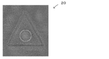
- FIG. 5 is an example of a STEM image by the DPC method of the magnetic element 20 when a magnetic field of 20 mT is applied in a direction perpendicular to the surface S at a temperature of 300K.
- FIG. 6 is a schematic diagram schematically showing the STEM image of FIG.
- FIG. 7 is an example of an STEM image of the magnetic element 20 by the DPC method when a magnetic field of 60 mT is applied in a direction perpendicular to the surface S at a temperature of 300K.
- a schematic diagram schematically showing the STEM image of FIG. 7 is almost the same as FIG. FIG.
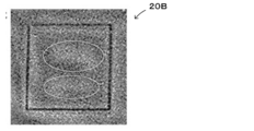
- FIG. 8 is an example of a STEM image by the DPC method of the magnetic element 20B of the comparative example when a magnetic field of 20 mT is applied in a direction perpendicular to the surface S at a temperature of 300K.
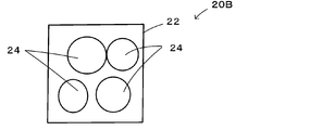
- FIG. 9 is a schematic diagram schematically showing the STEM image of FIG.
- FIG. 10 is an example of a STEM image by the DPC method of the magnetic element 20B of the comparative example when a magnetic field of 60 mT is applied in a direction perpendicular to the surface S at a temperature of 300K.
- FIG. 11 is a schematic diagram schematically showing the STEM image of FIG. FIG.
- FIG. 12 is an example of a STEM image by a DPC method of a magnetic element 20C of a comparative example when a magnetic field of 20 mT is applied in a direction perpendicular to the surface S at a temperature of 300K.
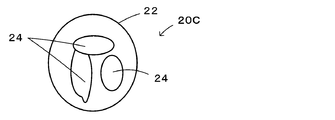
- FIG. 13 is a schematic diagram schematically showing the STEM image of FIG.
- FIG. 14 is an example of a STEM image by a DPC method of a magnetic element 20C of a comparative example when a magnetic field of 60 mT is applied in a direction perpendicular to the surface S at a temperature of 300K.
- FIG. 15 is a schematic diagram schematically showing the STEM image of FIG.
- the magnetic element 20B of the comparative example is an element in which a defect is introduced at a position corresponding to each side of a substantially square in the plan view of the surface S.
- a defect is introduced at a position corresponding to a substantially circular circumference in a plan view of the surface S.
- skyrmions are generated in portions surrounded by white circles.
- the skyrmion is at a higher temperature than the magnetic elements 20B and 20C of the comparative example, particularly at room temperature (such as 293 ⁇ 15 K which is a room temperature defined by JIS standards). It can be held more stably.
- FIG. 16 is a flowchart illustrating an example of a method for manufacturing the magnetic device 10.
- a substrate suitable for crystal growth of Co 8 Zn 8 Mn 4 is prepared (process P100). Silicon (Si) or the like can be used as the substrate.
- Step P110 a Co 8 Zn 8 Mn 4 magnetic thin film is formed on the substrate (process P110).
- a Co 8 Zn 8 Mn 4 magnetic thin film is formed on the substrate by using a technique such as MBE (Molecular Beam Epitaxy) so that the (111) plane is parallel to the surface.
- MBE Molecular Beam Epitaxy
- the electron beam from the Schottky field emission electron gun operating at 200 kV is a point having a diameter of 2 nm in plan view at a position corresponding to each side of a substantially equilateral triangle having one side of 440 nm in plan view of the surface S.
- a plurality of defects 22 that are shaped concave portions are formed with an interval of 10 nm.
- the defect 22 is introduced at a position corresponding to each side of the substantially equilateral triangle rotated by 180 degrees from the substantially equilateral triangle having each side corresponding to the position where the defect 22 of the adjacent magnetic element 20 is introduced.
- a plurality of magnetic elements 20 are sequentially manufactured.
- the formation time of the defect 22 can be shortened as compared with the case where the linear concave portion is formed as the defect 22.
- the throughput at the time of forming the magnetic element 20 can be improved, and the throughput at the time of manufacturing the magnetic device 10 can be improved.
- the generated skyrmion 24 is formed by introducing the defect 22 into the magnetic material capable of generating the skyrmion 24 at a position corresponding to each side of the substantially triangular shape in plan view. Can be stably held at a higher temperature.
- one skyrmion 24 is generated in a region corresponding to a substantially triangular interior in a plan view of the magnetic element 20.
- two or more skyrmions 24 can be generated by changing the length of each side of the substantially triangular shape.
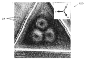
- 17 and 18 are explanatory diagrams showing an example of a STEM image by the DPC method of the magnetic element 120 according to the modification.
- the magnetic element 120 of the modified example has a plurality of defects 22 that are point-like concave portions having a diameter of 5 nm in plan view at positions corresponding to the sides of a substantially equilateral triangle having one side of 800 nm in plan view of the surface S. It is formed with an interval.
- FIG. 17 is an example of a STEM image by the DPC method of the magnetic element 120 of a modified example when a magnetic field of 60 mT is applied in a direction perpendicular to the surface S at a temperature of 295K.
- FIG. 18 is an example of a STEM image by a DPC method of the magnetic element 120 of a modified example when a magnetic field of 20 mT is applied in a direction perpendicular to the surface S at a temperature of 295 K.
- the magnetic element 120 as shown in FIG. 17, when a magnetic field of 60 mT is applied in a direction perpendicular to the surface S, one skyrmion 24 is generated in a region corresponding to the inside of a substantially equilateral triangle.
- the magnetic element 120 As shown in FIG. 18, when a magnetic field of 20 mT is applied in a direction perpendicular to the surface S, three skyrmions are generated in a region corresponding to the inside of a substantially equilateral triangle. In the magnetic element 120, when the applied magnetic field is increased from 20 mT, the number of generated skyrmions is switched from three to one at about 40 mT (40 mT ⁇ 1.0 mT). In the magnetic element 120, when the applied magnetic field exceeds 77 mT, the skyrmion becomes unstable or disappears.
- the modified magnetic device 110 including a plurality of magnetic elements 120 can be operated as a memory.
- the defects 22 which are a plurality of concave portions in a plan view are introduced into the magnetic material.
- a linear defect may be introduced at a position corresponding to each side of the substantially equilateral triangle in a plan view of the magnetic material, or penetrated to a position corresponding to each side of the approximately equilateral triangle in the plan view of the magnetic material. Holes may be formed, or atoms of a different type from the atoms constituting the magnetic material may be introduced at positions corresponding to the sides of the substantially equilateral triangle in plan view of the magnetic material.
- the defect 22 is introduced at a position corresponding to each side of a substantially equilateral triangle having one side of 440 nm in plan view of the surface S of the magnetic element 20.
- the length of each side of the substantially equilateral triangle may be any length as long as it is within a range of ⁇ 3 to 5 times the diameter of the skillion generated in the region corresponding to the interior of the substantially equilateral triangle. Good.
- the defect 22 is introduced at a position corresponding to each side of the substantially equilateral triangle in the plan view of the surface S of the magnetic element 20, but the length of the two sides is changed to the substantially equilateral triangle. It is good also as a substantially isosceles triangle with substantially equal, a substantially triangular shape from which the length of each side differs.
- the magnetic element 20 is formed of Co 8 Zn 8 Mn 4, but any material can be used as long as it can generate skyrmions.
- the magnetic element 20 may be formed of a helical magnetic material having a B20 type crystal structure. Examples of the “helical magnetic material having a B20 crystal structure” include MnSi, MnGe, MnGeFe, FeGe, FeGeSi, FeCoSi, and Cu 2 OSeO 3 .
- the magnetic element 20 may have a laminated structure of a magnetic thin film capable of generating skyrmions and a metal. Examples of the “magnetic thin film” include Fe, Co, Ni, and the like. Examples of “metal” include Pt, Ir, W and the like.
- the magnetic element 20 may be formed of a polar magnetic semiconductor. Examples of the “polar magnetic semiconductor” include GaV 4 S 8 and GaV 4 Se 8 .
- the magnetic element 20 is made of Co 8 Zn 8 Mn 4, but any ferromagnetic metal may be used.
- the magnetic material is formed of Co 8 Zn 8 Mn 4 exhibiting helical magnetism, but any magnetic material capable of generating skyrmions may be used. Different magnetic materials may be used.
- the crystal orientation of the magnetic material is formed to be the (111) plane parallel to the surface S.
- any crystal material orientation may be used as long as it can generate skyrmions. May be formed to be different from the (111) plane in parallel with the surface S.
- the magnetic element 20 is defective at a position corresponding to each side of a substantially triangular shape obtained by rotating a substantially triangular shape having each side corresponding to a position where a defect of an adjacent magnetic element is introduced by 180 degrees. 22 is introduced, but the defect 22 is formed at a position corresponding to each side of the substantially triangular shape without rotating the substantial triangle having each side corresponding to the position where the defect 22 of the adjacent magnetic element is introduced by 180 degrees. It may be introduced.
- the present invention may be applied to any magnetic memory that can store information. Further, the present invention may be applied to a magnetic sensor that detects magnetism.
- the present invention can be used in the manufacturing industry of magnetic elements and magnetic devices.
Landscapes
- Engineering & Computer Science (AREA)
- Power Engineering (AREA)
- Physics & Mathematics (AREA)
- Manufacturing & Machinery (AREA)
- Condensed Matter Physics & Semiconductors (AREA)
- General Physics & Mathematics (AREA)
- Computer Hardware Design (AREA)
- Hall/Mr Elements (AREA)
- Recording Or Reproducing By Magnetic Means (AREA)
- Manufacturing Of Magnetic Record Carriers (AREA)
- Thin Magnetic Films (AREA)
- Magnetic Record Carriers (AREA)
Abstract
磁性材料により形成された磁気素子であって、磁性材料は、スキルミオンを生成可能な材料であり、平面視で略三角形の各辺に相当する位置に欠陥が導入されている。欠陥が導入された磁性材料に対して、略三角形の内部に相当する領域に少なくとも1つのスキルミオンが生成する方向および強さの磁場を印加することにより、略三角形の内部に相当する領域内にスキルミオンを生成することができる。こうして生成したスキルミオンはより高い温度で安定して保持することができる。
Description
本発明は、磁気素子、磁気装置および磁気素子の製造方法に関し、詳しくは、磁性材料により形成された磁気素子、こうした磁気素子を複数備える磁気装置、磁性材料により形成された磁気素子の製造方法に関する。
従来、この種の磁気素子としては、らせん型の磁気構造を有する磁性材料により形成されるものが提案されている(例えば、特許文献1参照)。この磁気素子では、磁性材料は、板状に形成されている。そして、磁性材料に一定の磁場を印加した状態で、磁性体を加熱して29Kより高温とし、その後、磁性体を急冷して27Kより低温とすることにより、スキルミオンを準安定的に生成し保持する。そして、磁性体を加熱して27Kより高温とすることで、スキルミオンを消去している。
さらに、この種の磁気素子としては、スキルミオンを室温で生成可能な磁性材料あるいはスキルミオンを室温で生成可能な積層磁性薄膜により形成されるものが提案されている(例えば、非特許文献1,2など)。
しかしながら、上述の特許文献1の磁気素子では、生成したスキルミオンを27Kより高い温度で安定して保持することができない。また、上述の非特許文献1,2の磁気素子では、27Kより高い温度でスキルミオンを生成可能であるが、27Kより高い温度で熱揺らぎの影響に対抗して安定して保持することができない。磁気素子をディスクリートトラックメディアなど27Kより高い温度(例えば、JIS規格で定められる室温(293±15K)など)で使用される磁気装置へ搭載する場合、生成したスキルミオンを27Kより高い温度で安定して保持することが望まれている。
本発明は、生成したスキルミオンをより高い温度で安定して保持することが可能な磁気素子、磁気装置を提供することを主目的とする。本発明の磁気素子の製造方法では、生成したスキルミオンをより高い温度で安定して保持することができる磁気素子を製造することを主目的とする。
本発明の磁気素子、磁気装置、磁気素子の製造方法は、上述の主目的を達成するために以下の手段を採った。
本発明の磁気素子は、
磁性材料により形成された磁気素子であって、
前記磁性材料は、スキルミオンを生成可能な材料であり、
平面視で略三角形の各辺に相当する位置に欠陥が導入されている、
ことを要旨とする。
磁性材料により形成された磁気素子であって、
前記磁性材料は、スキルミオンを生成可能な材料であり、
平面視で略三角形の各辺に相当する位置に欠陥が導入されている、
ことを要旨とする。
この本発明の磁気素子では、磁性材料には、スキルミオンを生成可能な材料であり、平面視で略三角形の各辺に相当する位置に欠陥が導入されている。この磁気素子では、略三角形の内部に相当する領域に少なくとも1つのスキルミオンが生成する方向および強さの磁場を印加することにより、略三角形の内部に相当する領域内にスキルミオンを生成することができる。こうして生成したスキルミオンはより高い温度安定して保持することができる。これにより、スキルミオンをより高い温度で安定して保持可能な磁気素子を提供することができる。
こうした本発明の磁気素子において、前記略三角形の内部に相当する領域に少なくとも1つのスキルミオンが生成されていてもよい。
また、本発明の磁気素子において、平面視で点状の複数の欠陥が、生成されるスキルミオンの直径より短い間隔を持って前記各辺に相当する位置に並んで全体として三角形状に配置されていてもよい。この場合において、前記を形成してもよい。こうすれば、線状の複数の欠陥を形成するものに比して、製造時間の短縮を図ることができる。これにより、製造時のスループットが向上された磁気素子を提供することができる。
さらに、本発明の磁気素子において、平面視で線状の欠陥が、前記各辺に相当する位置に三角形状に配置されていてもよい。こうすれば、平面視で線状の欠陥を、各辺に相当する位置に三角形状に配置することにより、平面視で略三角形の各辺に相当する位置に欠陥を配置することができる。
そして、本発明の磁気素子において、前記欠陥は、一面に形成された凹部または凸部としてもよいし、前記欠陥は、貫通孔としてもよい。こうすれば、一面に形成された凹部または凸部や貫通孔により平面視で略三角形の各辺に相当する位置に欠陥を導入することができる。
また、本発明の磁気素子において、前記欠陥は、前記磁性材料に添加され、前記磁性材料を構成する原子と異なる種類の原子としてもよい。
さらに、本発明の磁気素子において、前記各辺の長さは、生成されるスキルミオンの直径の√3倍以上5倍以下の範囲内としてもよい。こうすれば、略三角形状の内部に1つまたは3つのスキルミオンを生成することができる。
そして、本発明の磁気素子において、前記磁性材料は、強磁性金属としたり、前記磁性材料は、らせん磁性を示す金属としたり、前記磁性材料は、CoZnMnの合金としてもよい。この場合において、磁性材料は、結晶方位が前記一面と平行に(111)面となるように形成してもよい。こうすれば、スキルミオンをより高い温度でより安定して保持することができる。
また、本発明の磁気素子において、前記磁性材料は、CoZnMnの合金であり、前記各辺の長さは、一辺の長さが150nm以上800nm以下の範囲内としてもよい。こうすれば、略三角形状の内部に1つまたは3つのスキルミオンを生成することができる。この場合において、前記磁性材料は、結晶方位が前記一面と平行に(111)面となるように形成してもよい。こうすれば、略三角形状の内部に1つまたは3つのスキルミオンをより高い温度でより安定して保持することができる。
本発明の磁気装置は、
上述したいずれかの態様の本発明の磁気素子、例えば、磁性材料により形成された磁気素子であって、前記磁性材料は、スキルミオンを生成可能な材料であり、平面視で略三角形の各辺に相当する位置に欠陥が導入されている、磁気素子を複数備えることを要旨とする。
上述したいずれかの態様の本発明の磁気素子、例えば、磁性材料により形成された磁気素子であって、前記磁性材料は、スキルミオンを生成可能な材料であり、平面視で略三角形の各辺に相当する位置に欠陥が導入されている、磁気素子を複数備えることを要旨とする。
この本発明の磁気装置では、上述したいずれかの態様の本発明の磁気素子を備えているから、本発明の磁気素子が備える効果、例えば、スキルミオンをより高い温度で安定して保持可能な磁気素子を提供することができる効果などと同様の効果を奏する。
こうした本発明の磁気装置において、前記複数の磁気素子は、隣の前記磁気素子の欠陥が導入された位置に相当する各辺を有する略三角形を180度回転させた略三角形の各辺に相当する位置に欠陥が導入されていてもよい。こうすれば、一定面積内により多くの磁気素子を配置することができる。
また、本発明の磁気装置を、情報を記憶可能な磁気メモリまたは磁気を検出する磁気センサとしてもよいし、ディスクリートトラックメディアとしてもよい。
本発明の磁気素子の製造方法は、
スキルミオンを生成可能な磁性材料により形成された磁気素子の製造方法であって、
前記磁性材料に、平面視で略三角形の各辺に相当する位置に欠陥を導入するに欠陥を導入する欠陥導入工程、
を備えることを要旨とする。
スキルミオンを生成可能な磁性材料により形成された磁気素子の製造方法であって、
前記磁性材料に、平面視で略三角形の各辺に相当する位置に欠陥を導入するに欠陥を導入する欠陥導入工程、
を備えることを要旨とする。
この本発明の磁気素子の製造方法では、欠陥導入工程では、磁性材料に、平面視で略三角形の各辺に相当する位置に欠陥を導入する。これにより、磁性材料には、スキルミオンを生成可能な材料であり、平面視で略三角形の各辺に相当する位置に欠陥が導入されている磁気素子を製造することができる。こうした磁気素子では、生成したスキルミオンをより高い温度で安定して保持することができる。よって、生成したスキルミオンをより高い温度で安定して保持することが可能な磁気素子を製造することができる。
こうした本発明の磁気素子の製造方法において、前記欠陥導入工程は、電子線を用いて、前記磁性材料に平面視で点状の複数の前記欠陥を導入する工程としてもよい。こうすれば、磁性材料に平面視で線状の欠陥を形成するものに比して、スループットの向上を図ることができる。
次に、本発明を実施するための形態を実施例を用いて説明する。
図1は、本発明の一実施例としての磁気装置10の構成の概略を示す構成図である。図2は、図1の部分Aを拡大した拡大図である。図3は、図2の部分Bを拡大した拡大図である。磁気装置10は、ディスクリートメディアとして構成されており、β-Mn型結晶構造を有するCo8Zn8Mn4のバルク多結晶の基板上に、複数の磁気素子20が同心円上に配置されてトラックを形成している。
複数の磁気素子20は、厚さが150nmで結晶方位が表面Sと平行に(111)面となるCo8Zn8Mn4により形成されている。Co8Zn8Mn4は、らせん磁性を示す磁性体の合金である。磁気素子20は、図2,図3に示すように、表面Sの平面視で1辺が440nmの略正三角形の各辺に相当する位置に、平面視で直径2nmで深さが数nm(例えば、1nm,2nm,3nmなど)の点状の凹部である複数の欠陥22が10nmの間隔を持って並んで形成されている。複数の磁気素子20は、隣の磁気素子20の欠陥22が導入された位置に相当する各辺を有する略正三角形が180度回転させた略正三角形の各辺に相当する位置に欠陥22が導入されている、すなわち、略正三角形と略逆正三角形とが交互に並ぶように欠陥22が導入されている。
こうして構成された実施例の磁気素子20では、室温(例えば、300K)で表面Sと垂直な方向に(図1~図3において図面の裏から表へ向かう方向に)20mT~80mTの磁場を印加することで、欠陥22で形成された略正三角形の内部に相当する領域内にスキルミオン24が生成される。図4は、温度が300Kで表面Sと垂直な方向に20mTの磁場を印加したときの、磁気装置10の要部の微分位相コントラスト(DPC)法による走査型透過電子顕微鏡(STEM)像の一例を示す説明図である。スキルミオン24は、平面視で半径120nmの略円形状に生成される。このスキルミオン24は、80mTを超える磁場を印加することで消滅する。そして、スキルミオン24が生成されているときと消滅しているときとをそれぞれ1ビットの情報に対応させて、表面Sと垂直な方向の磁場をトンネル磁気抵抗(TMR:Tunneling Magneto Resistance)素子などのセンサで検出することにより磁気装置10をメモリとして動作させることができる。なお、微分位相コントラスト(DPC)法による走査型透過電子顕微鏡(STEM)像とは、電子銃を用いて試料に電子線を入射させ、入射した電子線が試料内部の磁場で偏向されることによって、試料を挟んで電子銃と反対側の分割検出器の各位置で検出される電子線強度に差が生じることを利用して、試料上の各点での磁場を計測し、計測結果を可視化した像である。
図5は、温度が300Kで表面Sと垂直な方向に20mTの磁場を印加したときの磁気素子20のDPC法によるSTEM像の一例である。図6は、図5のSTEM像を模式的に表した模式図である。図7は、温度が300Kで表面Sと垂直な方向に60mTの磁場を印加したときの磁気素子20のDPC法によるSTEM像の一例である。なお、図7のSTEM像を模式的に表した模式図は、図7とほぼ同一の図面となるので記載を省略する。図8は、温度が300Kで表面Sと垂直な方向に20mTの磁場を印加したときの比較例の磁気素子20BのDPC法によるSTEM像の一例である。図9は、図8のSTEM像を模式的に表した模式図である。図10は、温度が300Kで表面Sと垂直な方向に60mTの磁場を印加したときの比較例の磁気素子20BのDPC法によるSTEM像の一例である。図11は、図10のSTEM像を模式的に表した模式図である。図12は、温度が300Kで表面Sと垂直な方向に20mTの磁場を印加したときの比較例の磁気素子20CのDPC法によるSTEM像の一例である。図13は、図12のSTEM像を模式的に表した模式図である。図14は、温度が300Kで表面Sと垂直な方向に60mTの磁場を印加したときの比較例の磁気素子20CのDPC法によるSTEM像の一例である。図15は、図14のSTEM像を模式的に表した模式図である。比較例の磁気素子20Bは、表面Sの平面視で略正方形の各辺に相当する位置に欠陥を導入した素子である。比較例の磁気素子20Cは、表面Sの平面視で略円形の円周に相当する位置に欠陥を導入したものである。図5,図6,図8,図10,図12,図14では、白丸で囲んだ部分にスキルミオンが生成されている。
実施例の磁気素子20では、図5,図6に示すように、印加する磁場が変化しても安定した平面視で略円形状の1つのスキルミオンが平面視で略三角形の内部に相当する領域内に生成されている。比較例の磁気素子20Bでは、印加する磁場が変化すると、平面視で略正方形の内部に相当する領域内に生成されるスキルミオンの形状と個数とが変化している。比較例の磁気素子20Cでは、印加する磁場が変化すると、平面視で略円形の内部に相当する領域内に生成されるスキルミオンの数が変化している。このように、実施例の磁気素子20では、比較例の磁気素子20B,20Cに比して、スキルミオンをより高い温度、特に、室温(JIS規格で定められる室温である293±15Kなど)でより安定して保持することができる。
次に、こうして構成された磁気装置10の製造方法について説明する。図16は、磁気装置10の製造方法の一例を示すフローチャートである。
最初に、Co8Zn8Mn4の結晶成長に適した基板を準備する(工程P100)。基板として、シリコン(Si)などが使用できる。
次に、基板上にCo8Zn8Mn4磁性体薄膜を形成する(工程P110)。工程P110では、表面と平行に(111)面となるようにMBE(モレキュラービームエピタキシー)法などの手法を用いて、基板上にCo8Zn8Mn4磁性体薄膜を形成する。
そして、磁性体薄膜の表面に凹部を形成して、すなわち、欠陥22を導入して(工程P120)、磁気装置10を完成する。工程P120では、200kVで動作するショットキー電界放出電子銃からの電子線で、表面Sの平面視で1辺が440nmの略正三角形の各辺に相当する位置に、平面視で直径2nmの点状の凹部である複数の欠陥22を10nmの間隔を持って形成する。そして、隣の磁気素子20の欠陥22が導入された位置に相当する各辺を有する略正三角形が180度回転させた略正三角形の各辺に相当する位置に欠陥22が導入されるように複数の磁気素子20を順次製造する。ここでは、欠陥22として点状の凹部を形成するから、欠陥22として線状の凹部を形成するときに比して、欠陥22の形成時間を短縮することができる。これにより、磁気素子20を形成する際のスループットの向上を図ることができ、磁気装置10を製造する際のスループットの向上を図ることができる。
以上説明した実施例の磁気装置10によれば、スキルミオン24を生成可能な磁性材料に、平面視で略三角形の各辺に相当する位置に欠陥22を導入することにより、生成したスキルミオン24をより高い温度で安定して保持することができる。
実施例の磁気装置10では、磁気素子20の平面視で略三角形の内部に相当する領域に1つのスキルミオン24が生成されている。しかしながら、略三角形の各辺の長さを変更することにより2つ以上のスキルミオン24を生成することができる。図17,図18は、変形例の磁気素子120のDPC法によるSTEM象の一例を示す説明図である。変形例の磁気素子120は、表面Sの平面視で1辺が800nmの略正三角形の各辺に相当する位置に、平面視で直径5nmの点状の凹部である複数の欠陥22を10nmの間隔を持って形成されている。
図17は、温度が295Kで表面Sと垂直な方向に60mTの磁場を印加したときの変形例の磁気素子120のDPC法によるSTEM像の一例である。図18は、温度が295Kで表面Sと垂直な方向に20mTの磁場を印加したときの変形例の磁気素子120のDPC法によるSTEM像の一例である。磁気素子120では、図17に示すように、表面Sと垂直な方向に60mTの磁場を印加すると、略正三角形の内部に相当する領域内に1つのスキルミオン24が生成される。磁気素子120では、図18に示すように、表面Sと垂直な方向に20mTの磁場を印加すると、略正三角形の内部に相当する領域内に3つのスキルミオンが生成される。磁気素子120では、印加する磁場を20mTから増加させると40mT程度(40mT±1.0mT)で、生成されるスキルミオンの個数が3つから1つへと切り換わる。磁気素子120では、印加する磁場が77mTを超えると、スキルミオンが不安定になったり、消滅したりする。したがって、磁気素子120では、スキルミオン24が1つ生成されている状態と3つ生成されている状態と消滅している状態とをそれぞれ1ビットに対応させて、表面Sと垂直な方向の磁場をトンネルTMR素子などのセンサで検出することにより磁気素子120を複数備える変形例の磁気装置110をメモリとして動作させることができる。
実施例の磁気装置10では、平面視で点状の複数の凹部である欠陥22を磁性材料へ導入している。しかしながら、磁性材料の平面視で略正三角形の各辺に相当する位置に何らかの欠陥を導入すればよいから、点状の複数の凹部に代えて凸部である欠陥を磁性材料へ導入してもよいし、磁性材料の平面視で略正三角形の各辺に相当する位置に線状の欠陥を導入してもよいし、磁性材料の平面視で略正三角形の各辺に相当する位置に貫通孔を形成してもよいし、磁性材料の平面視で略正三角形の各辺に相当する位置に磁性材料を構成する原子と異なる種類の原子を導入してもよい。
実施例の磁気装置10では、磁気素子20の表面Sの平面視で1辺が440nmの略正三角形の各辺に相当する位置に欠陥22が導入されている。しかしながら、略正三角形の各辺の長さは、略正三角形の内部に相当する領域内に生成されるスキルミオンの直径の√3倍以上5倍以下の範囲内であれば如何なる長さとしてもよい。
実施例の磁気装置10では、磁気素子20の表面Sの平面視で略正三角形の各辺に相当する位置に欠陥22が導入されているが、略正三角形に変えて、二辺の長さがほぼ等しい略二等辺三角形や、各辺の長さが異なる略三角形などとしてもよい。
実施例の磁気装置10では、磁気素子20をCo8Zn8Mn4により形成しているが、スキルミオンを生成可能な材料であれば、如何なるものを用いても構わない。また、磁気素子20をB20型結晶構造を有するらせん磁性材料により形成してもよい。「B20型結晶構造を有するらせん磁性材料」としては、MnSi,MnGe,MnGeFe,FeGe,FeGeSi,FeCoSi,Cu2OSeO3などを挙げることができる。さらに、磁気素子20をスキルミオンを生成可能な磁性薄膜と金属との積層構造としてもよい。「磁性薄膜」としては、Fe,Co,Niなどを挙げることができる。「金属」としては、Pt,Ir,Wなどを挙げることができる。そして、磁気素子20を極性磁性半導体により形成してもよい。「極性磁性半導体」としては、GaV4S8,GaV4Se8などを挙げることができる。
実施例の磁気装置10では、磁気素子20をCo8Zn8Mn4により形成しているが、強磁性金属であれば如何なるものを用いても構わない。
実施例の磁気装置10では、磁性材料をらせん磁性を示すCo8Zn8Mn4により形成しているが、スキルミオンを生成可能な磁性材料であれば如何なるものとしてもよいから、らせん磁性とは異なる磁性材料としてもよい。
実施例の磁気装置10では、磁性材料の結晶方位が表面Sと並行に(111)面となるように形成されているが、スキルミオンを生成可能なものであればよく、磁性材料の結晶方位が表面Sと並行に(111)面とな異なる面となるように形成してもよい。
実施例の磁気装置10では、磁気素子20を、隣の磁気素子の欠陥が導入された位置に相当する各辺を有する略三角形を180度回転させた略三角形の各辺に相当する位置に欠陥22を導入しているが、隣の磁気素子の欠陥22が導入された位置に相当する各辺を有する略三角形を180度回転させずにこの略三角形の各辺に相当する位置に欠陥22を導入してもよい。
実施例では、本発明をディスクリートトラックメディアに適用する場合について例示しているが、情報を記憶可能な磁気メモリであれば如何なるものに適用しても構わない。また、本発明を磁気を検出する磁気センサに適用しても構わない。
以上、本発明を実施するための形態について実施例を用いて説明したが、本発明はこうした実施例に何等限定されるものではなく、本発明の要旨を逸脱しない範囲内において、種々なる形態で実施し得ることは勿論である。
本発明は、磁気素子や磁気装置の製造産業などに利用可能である。
Claims (19)
- 磁性材料により形成された磁気素子であって、
前記磁性材料は、スキルミオンを生成可能な材料であり、
平面視で略三角形の各辺に相当する位置に欠陥が導入されている、
磁気素子。 - 請求項1記載の磁気素子であって、
前記略三角形の内部に相当する領域に少なくとも1つのスキルミオンが生成されている、
磁気素子。 - 請求項1または2記載の磁気素子であって、
平面視で複数の点状の欠陥が、生成されるスキルミオンの直径より短い間隔を持って前記各辺に相当する位置に並んで全体として三角形状に配置されている、
磁気素子。 - 請求項1または2記載の磁気素子であって、
平面視で線状の欠陥が、前記各辺に相当する位置に三角形状に配置されている、
磁気素子。 - 請求項1ないし4のいずれか1つの請求項に記載の磁気素子であって、
前記欠陥は、一面に形成された凹部または凸部である、
磁気素子。 - 請求項1ないし4のいずれか1つの請求項に記載の磁気素子であって、
前記欠陥は、貫通孔である、
磁気素子。 - 請求項1ないし4のいずれか1つの請求項に記載の磁気素子であって、
前記欠陥は、前記磁性材料に添加され、前記磁性材料を構成する原子と異なる種類の原子である、
磁気素子。 - 請求項1ないし7のいずれか1つの請求項に記載の磁気素子であって、
前記各辺の長さは、生成されるスキルミオンの直径の√3倍以上5倍以下の範囲内である、
磁気素子。 - 請求項1ないし8のいずれか1つの請求項に記載の磁気素子であって、
前記磁性材料は、強磁性金属である、
磁気素子。 - 請求項1ないし8のいずれか1つの請求項に記載の磁気素子であって、
前記磁性材料は、らせん磁性を示す金属である、
磁気素子。 - 請求項1ないし8のいずれか1つの請求項に記載の磁気素子であって、
前記磁性材料は、CoZnMnの合金である、
磁気素子。 - 請求項1ないし8のいずれか1つの請求項に記載の磁気素子であって、
前記磁性材料は、CoZnMnの合金であり、
前記各辺の長さは、一辺の長さが150nm以上800nm以下の範囲内である、
磁気素子。 - 請求項11または12記載の磁気素子であって、
前記磁性材料は、結晶方位が前記一面と平行に(111)面となるように形成されている、
磁気素子。 - 磁気装置であって、
請求項1ないし13のいずれか1つの請求項に記載の磁気素子を複数備える、
磁気装置。 - 請求項14記載の磁気装置であって、
前記複数の磁気素子は、隣の前記磁気素子の欠陥が導入された位置に相当する各辺を有する略三角形を180度回転させた略三角形の各辺に相当する位置に欠陥が導入されている、
磁気装置。 - 請求項14または15記載の磁気装置は、情報を記憶可能な磁気メモリまたは磁気を検出する磁気センサである、
磁気装置。 - 請求項14または15記載の磁気装置は、ディスクリートトラックメディアである、
磁気装置。 - スキルミオンを生成可能な磁性材料により形成された磁気素子の製造方法であって、
前記磁性材料に、平面視で略三角形の各辺に相当する位置に欠陥を導入する欠陥導入工程、
を備える磁気素子の製造方法。 - 請求項18記載の磁気素子の製造方法であって、
前記欠陥導入工程は、電子線を用いて、前記磁性材料に平面視で点状の複数の前記欠陥を導入する工程である
磁気素子の製造方法。
Priority Applications (2)
| Application Number | Priority Date | Filing Date | Title |
|---|---|---|---|
| JP2019515737A JP7142362B2 (ja) | 2017-05-02 | 2018-05-01 | 磁気素子、磁気装置および磁気素子の製造方法 |
| US16/610,118 US20200243242A1 (en) | 2017-05-02 | 2018-05-01 | Magnetic element, magnetic device, and manufacturing method of magnetic element |
Applications Claiming Priority (2)
| Application Number | Priority Date | Filing Date | Title |
|---|---|---|---|
| US201762500222P | 2017-05-02 | 2017-05-02 | |
| US62/500,222 | 2017-05-02 |
Publications (1)
| Publication Number | Publication Date |
|---|---|
| WO2018203554A1 true WO2018203554A1 (ja) | 2018-11-08 |
Family
ID=64016121
Family Applications (1)
| Application Number | Title | Priority Date | Filing Date |
|---|---|---|---|
| PCT/JP2018/017423 Ceased WO2018203554A1 (ja) | 2017-05-02 | 2018-05-01 | 磁気素子、磁気装置および磁気素子の製造方法 |
Country Status (3)
| Country | Link |
|---|---|
| US (1) | US20200243242A1 (ja) |
| JP (1) | JP7142362B2 (ja) |
| WO (1) | WO2018203554A1 (ja) |
Cited By (3)
| Publication number | Priority date | Publication date | Assignee | Title |
|---|---|---|---|---|
| WO2020059542A1 (ja) * | 2018-09-18 | 2020-03-26 | 国立大学法人大阪大学 | スキルミオン回路及びスキルミオン回路の製造方法 |
| JP2020111810A (ja) * | 2019-01-16 | 2020-07-27 | 株式会社アルバック | CoZnMn膜の形成方法、および、CoZnMnターゲット |
| WO2025043318A1 (pt) * | 2023-08-31 | 2025-03-06 | Centro Nacional De Pesquisa Em Energia E Materiais | Nanoestrutura compreendendo um skyrmion isolado, processo de fabricação da mesma e seu uso em microscopia e sensoriamento |
Families Citing this family (1)
| Publication number | Priority date | Publication date | Assignee | Title |
|---|---|---|---|---|
| KR102258439B1 (ko) * | 2019-08-13 | 2021-05-31 | 한국표준과학연구원 | 도넛 형상의 스커미온을 형성하는 방법 |
Citations (2)
| Publication number | Priority date | Publication date | Assignee | Title |
|---|---|---|---|---|
| WO2016021403A1 (ja) * | 2014-08-07 | 2016-02-11 | 国立研究開発法人理化学研究所 | 記憶媒体、記録装置、データ処理装置、データ記録装置および通信装置 |
| US20160314827A1 (en) * | 2013-08-01 | 2016-10-27 | Thales | A Memory Device, Comprising at Least One Element and Associated Method Spintronics |
-
2018
- 2018-05-01 WO PCT/JP2018/017423 patent/WO2018203554A1/ja not_active Ceased
- 2018-05-01 US US16/610,118 patent/US20200243242A1/en not_active Abandoned
- 2018-05-01 JP JP2019515737A patent/JP7142362B2/ja active Active
Patent Citations (2)
| Publication number | Priority date | Publication date | Assignee | Title |
|---|---|---|---|---|
| US20160314827A1 (en) * | 2013-08-01 | 2016-10-27 | Thales | A Memory Device, Comprising at Least One Element and Associated Method Spintronics |
| WO2016021403A1 (ja) * | 2014-08-07 | 2016-02-11 | 国立研究開発法人理化学研究所 | 記憶媒体、記録装置、データ処理装置、データ記録装置および通信装置 |
Non-Patent Citations (1)
| Title |
|---|
| TOKUNAGA, Y. ET AL.: "A new class of chiral materials hosting magnetic skyrmions beyond room temperature", NATURE COMMUNICATIONS, 2 July 2015 (2015-07-02), XP055277857, Retrieved from the Internet <URL:http://www.nature.com/articles/ncomms8638> [retrieved on 20180711] * |
Cited By (4)
| Publication number | Priority date | Publication date | Assignee | Title |
|---|---|---|---|---|
| WO2020059542A1 (ja) * | 2018-09-18 | 2020-03-26 | 国立大学法人大阪大学 | スキルミオン回路及びスキルミオン回路の製造方法 |
| JP2020111810A (ja) * | 2019-01-16 | 2020-07-27 | 株式会社アルバック | CoZnMn膜の形成方法、および、CoZnMnターゲット |
| JP7149191B2 (ja) | 2019-01-16 | 2022-10-06 | 株式会社アルバック | CoZnMn膜の形成方法、および、CoZnMnターゲット |
| WO2025043318A1 (pt) * | 2023-08-31 | 2025-03-06 | Centro Nacional De Pesquisa Em Energia E Materiais | Nanoestrutura compreendendo um skyrmion isolado, processo de fabricação da mesma e seu uso em microscopia e sensoriamento |
Also Published As
| Publication number | Publication date |
|---|---|
| JP7142362B2 (ja) | 2022-09-27 |
| US20200243242A1 (en) | 2020-07-30 |
| JPWO2018203554A1 (ja) | 2020-03-12 |
Similar Documents
| Publication | Publication Date | Title |
|---|---|---|
| WO2018203554A1 (ja) | 磁気素子、磁気装置および磁気素子の製造方法 | |
| Lavrijsen et al. | Asymmetric magnetic bubble expansion under in-plane field in Pt/Co/Pt: Effect of interface engineering | |
| Takeguchi et al. | Fabrication of magnetic nanostructures using electron beam induced chemical vapour deposition | |
| JP2015154002A (ja) | スキルミオンのサイズと渦の向きの制御方法及びスキルミオン結晶 | |
| US20220196764A1 (en) | Magnetic element having an improved measurement range | |
| Li et al. | Electric-field control of the nucleation and motion of isolated three-fold polar vertices | |
| Moubah et al. | Discrete layer-by-layer magnetic switching in Fe/MgO (001) superlattices | |
| Del-Valle et al. | Imprinting skyrmions in thin films by ferromagnetic and superconducting templates | |
| KR20170126805A (ko) | 수직 자화막 및 이를 포함하는 자기 장치 | |
| Ruiz‐Zepeda et al. | Precession electron diffraction‐assisted crystal phase mapping of metastable c‐GaN films grown on (001) GaAs | |
| Weinert et al. | Structural, chemical, and magnetic investigation of a graphene/cobalt/platinum multilayer system on silicon carbide | |
| Cascales Sandoval et al. | Observation and formation mechanism of 360° domain wall rings in synthetic anti-ferromagnets with interlayer chiral interactions | |
| Kuchuk et al. | Measuring the depth profiles of strain/composition in AlGaN-graded layer by high-resolution x-ray diffraction | |
| Serrano-Ramón et al. | Improvement of domain wall conduit properties in cobalt nanowires by global gallium irradiation | |
| Chen et al. | The basis of organic spintronics: Fabrication of organic spin valves | |
| JP2005217422A (ja) | 磁気抵抗素子 | |
| Gogoi et al. | Field driven evolution of periodic antiferromagnetic skyrmion non-centrosymmetric semiconducting monolayer | |
| Berzins et al. | Characterization of microscopic ferromagnetic defects in thin films using magnetic microscope based on Nitrogen-Vacancy centres | |
| Córdoba et al. | Manipulating the switching in modulated iron nanowires grown by focused electron beam induced deposition | |
| Andrieu et al. | Magnetotransport in MgO-based magnetic tunnel junctions grown by molecular beam epitaxy | |
| Rizwan et al. | Influence of growth temperature on microstructural and electromagnetic properties of nickel thin films | |
| Kurdi | Sustainable heusler and antiferromagnetic thin films for high density data storage | |
| Abes et al. | Effect of nanostructuration on the magnetic properties of CoPt films | |
| Bolotov et al. | Changes in morphology and local conductance of GeTe–Sb2Te3 superlattice films on silicon observed by scanning probe microscopy in a lithography mode | |
| Bull | Development of MTJs and antiferromagnetic materials for spintronic applications |
Legal Events
| Date | Code | Title | Description |
|---|---|---|---|
| 121 | Ep: the epo has been informed by wipo that ep was designated in this application |
Ref document number: 18793966 Country of ref document: EP Kind code of ref document: A1 |
|
| ENP | Entry into the national phase |
Ref document number: 2019515737 Country of ref document: JP Kind code of ref document: A |
|
| NENP | Non-entry into the national phase |
Ref country code: DE |
|
| 122 | Ep: pct application non-entry in european phase |
Ref document number: 18793966 Country of ref document: EP Kind code of ref document: A1 |