WO2018198729A1 - 3次元画像素子および光レーダー装置 - Google Patents
3次元画像素子および光レーダー装置 Download PDFInfo
- Publication number
- WO2018198729A1 WO2018198729A1 PCT/JP2018/014813 JP2018014813W WO2018198729A1 WO 2018198729 A1 WO2018198729 A1 WO 2018198729A1 JP 2018014813 W JP2018014813 W JP 2018014813W WO 2018198729 A1 WO2018198729 A1 WO 2018198729A1
- Authority
- WO
- WIPO (PCT)
- Prior art keywords
- light
- dimensional image
- image element
- signal
- pixel
- Prior art date
- Legal status (The legal status is an assumption and is not a legal conclusion. Google has not performed a legal analysis and makes no representation as to the accuracy of the status listed.)
- Ceased
Links
Images


Classifications
-
- H—ELECTRICITY
- H04—ELECTRIC COMMUNICATION TECHNIQUE
- H04N—PICTORIAL COMMUNICATION, e.g. TELEVISION
- H04N13/00—Stereoscopic video systems; Multi-view video systems; Details thereof
- H04N13/20—Image signal generators
- H04N13/204—Image signal generators using stereoscopic image cameras
- H04N13/254—Image signal generators using stereoscopic image cameras in combination with electromagnetic radiation sources for illuminating objects
-
- G—PHYSICS
- G01—MEASURING; TESTING
- G01C—MEASURING DISTANCES, LEVELS OR BEARINGS; SURVEYING; NAVIGATION; GYROSCOPIC INSTRUMENTS; PHOTOGRAMMETRY OR VIDEOGRAMMETRY
- G01C3/00—Measuring distances in line of sight; Optical rangefinders
- G01C3/02—Details
- G01C3/06—Use of electric means to obtain final indication
-
- G—PHYSICS
- G01—MEASURING; TESTING
- G01S—RADIO DIRECTION-FINDING; RADIO NAVIGATION; DETERMINING DISTANCE OR VELOCITY BY USE OF RADIO WAVES; LOCATING OR PRESENCE-DETECTING BY USE OF THE REFLECTION OR RERADIATION OF RADIO WAVES; ANALOGOUS ARRANGEMENTS USING OTHER WAVES
- G01S17/00—Systems using the reflection or reradiation of electromagnetic waves other than radio waves, e.g. lidar systems
- G01S17/88—Lidar systems specially adapted for specific applications
- G01S17/89—Lidar systems specially adapted for specific applications for mapping or imaging
- G01S17/894—Three-dimensional [3D] imaging with simultaneous measurement of time-of-flight at a two-dimensional [2D] array of receiver pixels, e.g. time-of-flight cameras or flash lidar
-
- G—PHYSICS
- G01—MEASURING; TESTING
- G01S—RADIO DIRECTION-FINDING; RADIO NAVIGATION; DETERMINING DISTANCE OR VELOCITY BY USE OF RADIO WAVES; LOCATING OR PRESENCE-DETECTING BY USE OF THE REFLECTION OR RERADIATION OF RADIO WAVES; ANALOGOUS ARRANGEMENTS USING OTHER WAVES
- G01S7/00—Details of systems according to groups G01S13/00, G01S15/00, G01S17/00
- G01S7/48—Details of systems according to groups G01S13/00, G01S15/00, G01S17/00 of systems according to group G01S17/00
- G01S7/483—Details of pulse systems
- G01S7/486—Receivers
- G01S7/4861—Circuits for detection, sampling, integration or read-out
- G01S7/4863—Detector arrays, e.g. charge-transfer gates
-
- G—PHYSICS
- G01—MEASURING; TESTING
- G01S—RADIO DIRECTION-FINDING; RADIO NAVIGATION; DETERMINING DISTANCE OR VELOCITY BY USE OF RADIO WAVES; LOCATING OR PRESENCE-DETECTING BY USE OF THE REFLECTION OR RERADIATION OF RADIO WAVES; ANALOGOUS ARRANGEMENTS USING OTHER WAVES
- G01S7/00—Details of systems according to groups G01S13/00, G01S15/00, G01S17/00
- G01S7/48—Details of systems according to groups G01S13/00, G01S15/00, G01S17/00 of systems according to group G01S17/00
- G01S7/483—Details of pulse systems
- G01S7/486—Receivers
- G01S7/4865—Time delay measurement, e.g. time-of-flight measurement, time of arrival measurement or determining the exact position of a peak
-
- G—PHYSICS
- G01—MEASURING; TESTING
- G01S—RADIO DIRECTION-FINDING; RADIO NAVIGATION; DETERMINING DISTANCE OR VELOCITY BY USE OF RADIO WAVES; LOCATING OR PRESENCE-DETECTING BY USE OF THE REFLECTION OR RERADIATION OF RADIO WAVES; ANALOGOUS ARRANGEMENTS USING OTHER WAVES
- G01S7/00—Details of systems according to groups G01S13/00, G01S15/00, G01S17/00
- G01S7/48—Details of systems according to groups G01S13/00, G01S15/00, G01S17/00 of systems according to group G01S17/00
- G01S7/483—Details of pulse systems
- G01S7/486—Receivers
- G01S7/487—Extracting wanted echo signals, e.g. pulse detection
-
- H—ELECTRICITY
- H04—ELECTRIC COMMUNICATION TECHNIQUE
- H04N—PICTORIAL COMMUNICATION, e.g. TELEVISION
- H04N13/00—Stereoscopic video systems; Multi-view video systems; Details thereof
- H04N13/20—Image signal generators
- H04N13/271—Image signal generators wherein the generated image signals comprise depth maps or disparity maps
-
- H—ELECTRICITY
- H10—SEMICONDUCTOR DEVICES; ELECTRIC SOLID-STATE DEVICES NOT OTHERWISE PROVIDED FOR
- H10F—INORGANIC SEMICONDUCTOR DEVICES SENSITIVE TO INFRARED RADIATION, LIGHT, ELECTROMAGNETIC RADIATION OF SHORTER WAVELENGTH OR CORPUSCULAR RADIATION
- H10F39/00—Integrated devices, or assemblies of multiple devices, comprising at least one element covered by group H10F30/00, e.g. radiation detectors comprising photodiode arrays
- H10F39/10—Integrated devices
- H10F39/12—Image sensors
- H10F39/18—Complementary metal-oxide-semiconductor [CMOS] image sensors; Photodiode array image sensors
-
- H—ELECTRICITY
- H10—SEMICONDUCTOR DEVICES; ELECTRIC SOLID-STATE DEVICES NOT OTHERWISE PROVIDED FOR
- H10F—INORGANIC SEMICONDUCTOR DEVICES SENSITIVE TO INFRARED RADIATION, LIGHT, ELECTROMAGNETIC RADIATION OF SHORTER WAVELENGTH OR CORPUSCULAR RADIATION
- H10F39/00—Integrated devices, or assemblies of multiple devices, comprising at least one element covered by group H10F30/00, e.g. radiation detectors comprising photodiode arrays
- H10F39/80—Constructional details of image sensors
- H10F39/805—Coatings
- H10F39/8057—Optical shielding
-
- H—ELECTRICITY
- H10—SEMICONDUCTOR DEVICES; ELECTRIC SOLID-STATE DEVICES NOT OTHERWISE PROVIDED FOR
- H10F—INORGANIC SEMICONDUCTOR DEVICES SENSITIVE TO INFRARED RADIATION, LIGHT, ELECTROMAGNETIC RADIATION OF SHORTER WAVELENGTH OR CORPUSCULAR RADIATION
- H10F39/00—Integrated devices, or assemblies of multiple devices, comprising at least one element covered by group H10F30/00, e.g. radiation detectors comprising photodiode arrays
- H10F39/80—Constructional details of image sensors
- H10F39/806—Optical elements or arrangements associated with the image sensors
- H10F39/8063—Microlenses
Definitions
- the present invention relates to a three-dimensional image element that acquires a three-dimensional image composed of a two-dimensional image of a target object and distance information to the target object.
- 3D image is a concept that includes distance information to an object in the field of view in addition to a normal 2D image like a photograph.
- a three-dimensional image sensor for detecting a three-dimensional image has become extremely important as a sensor used for peripheral recognition of automobiles, robots, and the like.
- CCD and CMOS imagers are widely used as two-dimensional image sensors for detecting a two-dimensional image. Both CCD and CMOS imagers convert light intensity into electric signals and image them with silicon photodiodes.
- a method of measuring the time-of-flight until the laser beam is reflected on the object and returned from the object is widely used. I am doing.
- Non-Patent Document 1 As a method of irradiating the entire field of view with a laser beam, there are a scan type in which a laser beam focused in a dot or band shape is scanned by a mirror or the like, and a batch irradiation type in which a laser beam is spread almost uniformly over the entire field of view and irradiated.
- a scan type in which a laser beam focused in a dot or band shape is scanned by a mirror or the like
- a batch irradiation type in which a laser beam is spread almost uniformly over the entire field of view and irradiated.
- the batch irradiation type does not require a mechanical mechanism to scan, it is easy to miniaturize, but the laser light intensity on the object is weaker than the scan type, so when the distance to the object becomes long, The signal strength is weakened and the distance measurement accuracy is lowered.
- time-of-flight measurement in order for time measurement accuracy to be directly linked to distance accuracy, pulse laser light is emitted multiple times, time measurement from light emission to light reception is repeated, and a histogram (horizontal axis: time, vertical axis: frequency) is displayed. There is a way to configure and determine the flight time.
- This method is a method called TCSPC (Time-Correlated-Single-Photon-Counting).
- SPAD Single-Photon-Avalanche-Diode
- this light receiving element is not used in an imager in which large-scale pixels are two-dimensionally arranged because of a large circuit scale per pixel. Used in combination with the scan type.
- the current of the photodiode is measured and compared with the judgment value to determine the flight time.
- the current is sequentially accumulated in capacitors arranged in time series, and the flight time may be determined based on the accumulated amount. Because of this mechanism, a three-dimensional image is formed by a single laser irradiation. Therefore, in the case of a photograph, simultaneity is ensured over the entire field of view as if an image was taken by applying a flash.
- such a batch irradiation type is greatly different from a scan type in which time is different for each point of the visual field, and is described as “flash”.
- the scan type is not preferred because the miniaturization and durability of the device are extremely important.
- the countermeasure against background light becomes a problem.
- the optical radar device In automotive applications, the optical radar device must operate even under intense sunlight at midday just below the equator.
- a silicon type light receiving element In the sensor disclosed in Patent Document 1, in order to minimize the influence of background light during the day, a silicon type light receiving element cannot be used for the convenience of using infrared light having a wavelength of about 1.5 ⁇ m. The compound semiconductor must be used.
- the silicon LSI performs signal processing. For this reason, since the InGaAs photodiode and the silicon LSI have to be stacked, the sensor becomes a very expensive device due to increased costs in terms of materials and manufacturing processes.
- An object of one embodiment of the present invention is to realize an inexpensive three-dimensional image element having a wide measurement range.
- a three-dimensional image element includes an avalanche photodiode that detects photons of incident light including reflected light from an object to be detected in a Geiger mode.
- a light receiving unit having a plurality of pixels and a pulse signal provided as a one-to-one correspondence with the pixels, and outputting a pulse signal output from the pixels as a photon detection result for each series of time intervals arranged in time series.
- a calculation unit that calculates distance information about the distance between the light receiving unit and the object for each pixel using a series of integrated value groups arranged in a time series integrated by the integration unit. It has.
- (A) is a timing chart which shows the drive timing of the said pixel memory element
- (b) is a wave form diagram which expands and shows reflected pulsed light. It is a flowchart which shows the procedure of the signal processing by the signal processing circuit of the said three-dimensional image element. It is a flowchart which shows the procedure of the signal processing by the signal processing circuit in the three-dimensional image element of the optical radar apparatus which concerns on Embodiment 2 of this invention. It is a block diagram which shows the structure of the three-dimensional image element which comprises the optical radar apparatus which concerns on Embodiment 3 of this invention.
- Embodiment 1 The first embodiment of the present invention will be described with reference to FIGS. 1 to 9 as follows.
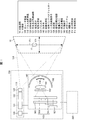
- FIG. 1 is a schematic diagram showing a configuration of an optical radar device 100 according to the present embodiment.
- the optical radar device 100 includes a pulsed light illumination system 110 that irradiates a target visual field 10 with pulsed light 124, and a light receiving system 140 that receives light from at least a part of the target visual field 10. Yes.
- the pulsed light illumination system 110 includes an illumination system power supply 120, a light emitting element driving circuit 121, a diffusion optical system 123, and a light emitting element 122.
- the diffusion optical system 123 collectively irradiates the entire target visual field 10 with the pulsed light 124 emitted from the light emitting element 122.
- the light emitting element driving circuit 121 is a circuit that drives the light emitting element 122 in pulses.
- the illumination system power source 120 is a power source that supplies power to the light emitting element driving circuit 121.
- the pulsed light illumination system 110 and the light receiving system 140 are provided close to each other. However, a structure in which the pulsed light 124 emitted from the pulsed light illumination system 110 does not leak into the light receiving system 140 except for the reflected light from the target object 11 to be detected in the target visual field 10 is preferable.
- the light receiving system 140 includes an imaging optical system 151, an optical band pass filter 152, a three-dimensional image element 153, a control element 160, and a light receiving system power supply 157.
- the three-dimensional image element 153 includes a light receiving unit 154 and a signal storage processing unit 155.
- the imaging optical system 151 forms an image of the reflected light from the target visual field 10 on the light receiving unit 154 of the three-dimensional image element 153.
- the control element 160 controls the three-dimensional image element 153 and the pulsed light illumination system 110 and communicates with the external system 300.
- the light receiving system power source 157 is a power source that supplies power to each unit of the light receiving system 140.
- the target visual field 10 is generally a rectangle characterized by a horizontal irradiation angle ⁇ h and a vertical irradiation angle ⁇ v, but is not limited to a rectangle and may be an elliptical shape.
- the pulsed light 124 is uniform in the target visual field 10, since the detection sensitivity of the place where the light intensity is strong becomes high, if there is a place that particularly needs to be watched in the target visual field 10, It is also possible to obtain a light intensity distribution with enhanced intensity in the vicinity.
- the diffusion optical system 123 is an optical system that irradiates and emits light from the light emitting element 122 into the target visual field 10, and includes a diffusion plate, a diffraction grating, a cylindrical lens, and the like.
- the light emitting element 122 is a light source capable of emitting pulses such as a laser and an LED, and preferably emits infrared light having a wavelength of about 700 nm to 1000 nm.
- an infrared laser is suitably used from the viewpoint that the light emission wavelength band is narrow and the temperature fluctuation of the light emission peak wavelength is preferably small.
- VCSEL Very / Cavity / Surface / Emitting / Laser
- a temperature control element that controls the temperature of the light emitting element 122 may be added to the pulsed light illumination system 110 in order to suppress temperature fluctuation of the emission peak wavelength.
- the light emitting element driving circuit 121 causes the light emitting element 122 to emit light in a pulsed manner by causing a predetermined current to flow through the light emitting element 122 at a predetermined timing.
- the light emission timing is determined by a signal from the control element 160.
- the amount of current of the light emitting element 122 may be variable or may be controlled by the control element 160. The same applies to the time change of the current that determines the emission time of the pulsed light 124.
- the half width (time) of the pulsed light 124 is about 1 nsec to several hundred nsec.
- the optical radar device 100 requires high-power pulsed light 124 of several tens to several hundreds W.
- the light emitting element driving circuit 121 generally discharges the charges to the light emitting element 122 at once after accumulating charges in the capacitor so as to form short pulse light. Therefore, the condenser and the switching element may be combined with the light emitting element 122 to be modularized.
- the illumination system power supply 120 has a normal logic circuit low voltage DC power supply and a high voltage DC power supply of several tens of volts for charging the capacitor. By controlling the output voltage of the high-voltage DC power supply or the charging time for the capacitor, the pulse emission power can be controlled. Further, the pulse width can be controlled by controlling the switching speed of the switching element. These controls can be performed by the control element 160.
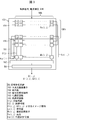
- FIG. 3 is a block diagram showing the configuration of the three-dimensional image element 153.
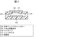
- FIG. 2 is a cross-sectional view of the package of the three-dimensional image element 153 constituting the optical radar device 100 according to the present embodiment.
- the imaging optical system 151 is generally a lens.
- the focal length and the F number can be selected depending on the size of the light receiving unit 154 and the viewing angle (FOV). It is preferable that the transmittance is high and the aberration is small at the center wavelength of the optical bandpass filter 152 described later.
- a lens is shown in FIG. 1, a reflective optical system other than a lens may be used instead of the lens.
- the optical bandpass filter 152 has a transmission band in a band with a constant width centering on the wavelength peak of pulsed light.
- the width of the transmission band (half width of the wavelength distribution of transmittance) is several nm to several tens of nm, and preferably about 10 nm to 20 nm.
- the peak temperature of the pulsed light changes with temperature due to the widening of the operating temperature range, so the pulsed light distribution needs to be within the transmission band at least in the operating temperature range. .
- the temperature shift of the peak wavelength is about 0.07 nm / degree
- the half width of the emission peak is about 1 nm
- the temperature shift of the transmission band center wavelength of the optical bandpass filter is 0.025 nm / degree. .
- the relative wavelength shift between the peak wavelength and the center wavelength of the transmission band is about 5.6 nm
- the optical bandpass filter has a transmission band of about 10 nm. 152 can be used.
- the flat interference filter When a flat interference filter generally used as the optical bandpass filter 152 is used, when the incident angle at which the reflected light is incident on the filter surface increases from 0 degree, the center wavelength of the transmission band shifts to the short wavelength side. Therefore, when the viewing angle is wide, the flat transmission filter may not be able to ensure the same transmission wavelength band in the entire target field 10.
- the flat interference filter is preferably shielded from the outside air because it may deteriorate and deteriorate over time when exposed to moisture or oxygen for a long time.
- a resin-made hemispherical dome transparent to infrared rays is provided as a protective cover 156 on the front surface of the imaging optical system 151 to protect the light receiving system 140 from the outside air.
- the protective cover 156 is provided, for example, the optical bandpass filter 152 can be provided on the surface of the imaging optical system 151 or the inner surface or inside of the protective cover 156.
- the optical bandpass filter 152 is provided on the protective cover 156, the hemispherical diameter of the protective cover 156 is set according to the diameter of the imaging optical system 151, so that each direction in the target visual field 10 can be set. A substantially constant transmission band can be secured for the reflected light.
- the diameter of the hemisphere As the diameter of the hemisphere is larger, the transmission band shift with respect to light condensed on each pixel Px (i, j) described later can be reduced. For this reason, the actual size of the diameter of the hemisphere can be determined by a trade-off between the outer shape of the optical radar device 100 and the reduction of the transmission band shift. In a practical range, the diameter of the hemisphere is preferably 5 times or more, more preferably 10 times or more the diameter of the imaging optical system 151.
- the optical bandpass filter 152 can be added inside the lid glass 171 as shown in FIG.
- the lid glass 171 constitutes an optical window of the package 170 that seals the three-dimensional image element 153.
- the sealed atmosphere 172 inside the package 170 preferably removes moisture and further preferably removes oxygen. This is to prevent the optical band pass filter 152 from aging. Therefore, the atmosphere 172 is preferably at least dry air, and more preferably nitrogen or argon, helium, or the like. Although omitted in FIG. 2, it is preferable to use a silicone resin with little oxygen and moisture permeation for bonding the lid glass 171 to the package 170.
- the optical band pass filter 152 may be incorporated in the imaging optical system 151. Although one optical bandpass filter 152 is shown in FIGS. 1 and 2, a plurality of optical bandpass filters 152 may be used.
- the first optical bandpass filter may be disposed on the front surface or the rear surface of the imaging optical system 151, and the second optical bandpass filter may be disposed on the inner surface of the lid glass 171 as described above. By providing the first optical bandpass filter, the light energy incident on the package 170 can be reduced, and an effect of suppressing a temperature rise can be obtained.
- the transmission band of the first optical bandpass filter is preferably wider than the transmission band of the second optical bandpass filter.
- the light receiving unit 154 and the signal storage processing unit 155 (integration unit and calculation unit) of the three-dimensional image element 153 can be formed on a silicon substrate.
- the light receiving unit 154 and the signal storage processing unit 155 are formed as separate chips, and may be combined using vertical via holes, bumps, and the like, and the respective chips may be stacked.
- the monolithic may be formed on the same silicon substrate. Preferably it is comprised.
- the light receiving unit 154 and the signal storage processing unit 155 are arranged in the upper and lower stages in the drawing. However, this is for the sake of convenience, and the light receiving unit 154 may be disposed in the center. However, it is not preferable that the light receiving unit 154 and the signal storage processing unit 155 are mixed. This is because the range in which the light receiving unit 154 exists is widened and the size of the imaging optical system 151 and the lid glass 171 is increased, resulting in an increase in cost.
- pixels Px (i, j) are arranged in a two-dimensional matrix of M rows and N columns.
- the pixel Px (i, j) has a function of detecting a photon by SPAD and outputting a pulse signal (pixel signal) as a photon detection result, as will be described later. All the pixels Px (i, j) are configured identically.
- the signal storage processing unit 155 includes a plurality of pixel storage elements Mx (i, j) (integrating units) corresponding to the respective pixels Px (i, j) arranged at least in a matrix.
- the pixel memory element Mx (i, j) is connected to each pixel Px (i, j) on a one-to-one basis by a signal line Lx (i, j).
- a photon (photon) is received by the pixel Px (i, j)
- a pixel signal (pulse signal) output as a photon detection result from the pixel Px (i, j) passes through the signal line Lx (i, j). Sent to the pixel storage element Mx (i, j) and stored therein.
- the signal storage processing unit 155 includes at least a row selection circuit 161 and a column selection circuit 162 (switching circuit) for selecting a specific pixel storage element Mx (i, j), and a signal processing circuit DS (calculation unit). Including.
- the signal processing circuit DS uses the distance information D (i, j) as an output signal based on the information stored in the specific pixel storage element Mx (i, j) selected by the row selection circuit 161 and the column selection circuit 162. ) And two-dimensional image information G1 (i, j), G2 (i, j) (two-dimensional image information) are calculated and output.
- the two-dimensional image information G1 (i, j), G2 (i, j) is the light intensity of the incident light (reflected light of the pulsed light) from the object 11 incident on each pixel Px (i, j). Is light intensity information for specifying a two-dimensional image of the object 11 based on each light intensity in the detection range.
- the difference between the two-dimensional image information G1 (i, j) and G2 (i, j) will be described later.
- the signal storage processing unit 155 is configured as follows.
- the row selection signal line R ⁇ (i) extends from, for example, the row selection circuit 161 to the pixel storage element Mx (i, j) in the i row.
- an ⁇ portion (a binary counter BC ⁇ described later) of the pixel storage element Mx (i, j) in the row i is selected.
- the column selection circuit 162 selects a specific column signal line C (j).
- the signal of the pixel storage element Mx (i, j) is read into the signal processing circuit DS, and the distance information D (i, j) and the two-dimensional image information G1 (i, j), G2 ( i, j) is output.
- the two-dimensional image information G1 (i, j) is two-dimensional image information (second light intensity information) of the object 11 with background light that does not include the reflected light of the pulsed light.
- the two-dimensional image information G2 (i, j) is two-dimensional image information (first light intensity information) of the object 11 by the reflected light of the pulsed light, but is not limited thereto.
- reading of the output signal from the pixel storage element Mx (i, j) is performed in parallel with the integration of the number of pulses of the pixel signal to the pixel storage element Mx (i, j). It can be carried out. As a result, a pixel with a strong signal intensity can be detected early.
- the pixel Px (i, j) having a high signal intensity captures a nearby object 11 and can detect the object 11 close to the three-dimensional image element at an early stage and issue an alarm. .
- the signal storage processing unit 155 stores the readout order of signals from the pixel storage element Mx (i, j), and can arbitrarily select the readout order. Thereby, the accumulated photons from the pixel storage element Mx (i, j) obtained by integrating the number of photons obtained from the pixel Px (i, j) from which the reflected light from the object 11 close to the three-dimensional image element is detected. The number can be read out early.
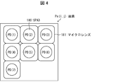
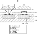
- FIG. 4 is a plan view showing the configuration of the pixel Px (i, j) of the three-dimensional image element 153.
- FIG. 5 is a cross-sectional view showing the configuration of the pixel Px (i, j).
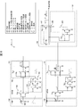
- FIG. 6 is a circuit diagram showing the configuration of the pixel Px (i, j) of the three-dimensional image element 153.
- the light receiving unit 154 has a plurality of pixels Px (i, j) arranged in a two-dimensional matrix of M rows and N columns.
- the light receiving unit 154 is supplied with a control signal, a power supply voltage, a clock CLK, and the like.
- the pixel Px (i, j) is composed of one or a plurality of SPAD (Single-Photon-Avalanche-diode) 180 (avalanche photodiode).
- the SPAD 180 is a photodiode that detects photons of incident light in a Geiger mode.
- Each SPAD 180 has a microlens 181 as shown in FIG.
- the structure of the SPAD 180 can take various forms, but will not be described in detail here.
- the SPAD 180 is configured by forming a P + diffusion layer 184 on the surface of an N-type diffusion layer 185 formed on the silicon substrate 183.
- the surface of the silicon substrate 183 is covered with a metal shield 182 at a predetermined interval.
- the metal shield 182 has an opening 182 a formed so as to expose a part of the P + diffusion layer 184.
- the opening 182 a forms an effective light receiving region, and allows light incident through the microlens 181 to pass to the P + diffusion layer 184.
- each SPAD 180 is arranged at substantially the same distance except for the lower right of the pixel portion where the circuit such as the output circuit is arranged. This is because the microlens 181 is used to collect as much light as possible to increase detection sensitivity. However, if the sensitivity is sufficient and the pixel area can be reduced on the circuit layout, each SPAD 180 may be arranged in a concentrated range.
- the optimum value of the SPAD total number Nspad varies depending on the number of photons Md received by one pixel during the dead time Td of the SPAD 180 to be used.
- Deadtime Td is the time required for one SPAD to detect the next photon after detecting one photon, and literally the length of time that SPAD does not function as a sensor. Generally, the length is about several nsec to 100 nsec.
- Md ⁇ 1 the total SPAD Nspad may be small or one. However, in the case where the number of photons Md can exceed 1, the number of photons that can be counted is 1 because one SPAD 180 cannot measure the period of the next Td at the stage of counting the first one.
- the SPAD total number Nspad must be increased. If the fill factor (ratio of the total area of the effective light receiving region to the pixel area) is the same, the detection sensitivity improves as the SPAD total number Nspad increases.
- the pixel Px (i, j) includes a SPAD control unit 190 and a photon detection signal generation unit 191 as a part attached to each SPAD 180.
- FIG. 6 shows waveforms of signals output from the SPAD control unit 190 and the units of the photon detection signal generation unit 191, respectively.
- the SPAD control unit 190 is a circuit that applies the power supply voltage VSPAD to the SPAD 180, quenches when a photon is detected in the pixel Px (i, j), and returns to the measurement state after Deadtime Td.
- the SPAD control unit 190 is simply illustrated as a circuit to which one resistor R is added except for the SPAD 180, assuming an inactive quench, but an active quench circuit may be used.
- Various circuits such as a circuit for controlling the activation of the SPAD 180 can also be added.
- the photon detection signal generator 191 is a circuit that detects an increase in the terminal voltage of the SPAD 180 and outputs one pulse having a certain width when the SPAD 180 detects a photon.
- FIG. 6 shows an example in which the photon detection signal generator 191 includes a first inverter 192, a second inverter 193, a delay circuit 194, and a NOR circuit 195.
- the delay circuit 194 is shown in FIG. 6 as an example composed of two stages of inverters, it may be composed of four or more stages of even stages of inverters, or may be a delay circuit of another configuration.
- the delay time of the delay circuit 194 determines the pulse width. The delay time is preferably about 0.1 nsec to several nsec.
- the NOR circuit 195 outputs a logical sum negation of the output of the first inverter 192 and the output of the second inverter 193.
- the pixel Px (i, j) has a pixel signal output circuit 196 that is common to the photon detection signal generators 191.
- the pixel signal output circuit 196 is a circuit that receives the photon detection signals from the respective SPADs 180 in parallel and sends out a pulse having substantially the same length as the photon detection signal to the signal line Lx (i, j). If a plurality of SPADs 180 emit photon detection signals almost simultaneously, they cannot be distinguished. In order to minimize such a case, the pulse width of the signal passing through the signal line Lx (i, j) can be made as short as possible.
- 6 illustrates an example in which the pixel signal output circuit 196 includes a signal line drive circuit 197, a signal line reset circuit 198, and a delay circuit 199.
- the present invention is not limited to this.
- the signal line drive circuit 197 is a circuit that receives a photon detection signal, supplies a current to the signal line Lx (i, j), raises the potential of the signal line Lx (i, j), and outputs a pixel signal. It operates completely in parallel for each photon detection signal.
- the pixel signal is a pulse signal corresponding to the photon detection signal.
- the signal line drive circuit 197 has a configuration in which NMOS transistors having gates that receive outputs from the photon detection signal generation units 191 are connected in parallel, but other configurations may be used.
- the signal line drive circuit 197 may be configured to receive an output from each photon detection signal generation unit 191 by an AND circuit and turn on one NMOS transistor having a large driving capability by the output of the AND circuit.
- the signal line drive circuit 197 has a capability of driving the signal delay time in the signal line Lx (i, j) in a short time, and must transmit a signal to the pixel storage element Mx (i, j). This delay time is determined by the driving capability of the transistor provided in the signal line drive circuit 197 with respect to the parasitic capacitance of the signal line Lx (i, j). This delay time is preferably at least equal to or less than the pulse width generated by the photon detection signal generator 191.
- the signal delay time in the signal line Lx (i, j) is preferably short, and the signal line Lx (i, j) is short. Is preferred.
- the signal line reset circuit 198 is a circuit that restores the potential of the signal line Lx (i, j) after being raised by the signal line drive circuit 197.
- the signal line reset circuit 198 includes the delay circuit 199 that delays the signal of the signal line Lx (i, j) and the signal line pull-down circuit 200.
- the delay circuit 199 is shown as a two-stage inverter chain, it may be an even-numbered inverter chain of four or more stages, or may be another delay circuit.
- the photon detection signal is a pulse that rises from the ground level to the Vcc level, but the same function can be realized even if it is a pulse that falls from the Vcc level to the ground level.
- the pulse width of the pixel signal passing through the signal line Lx (i, j) is substantially determined by the photon detection signal generator 191, but is determined by the pixel signal output circuit 196. It is also possible to use a configuration.
- the signal line Lx (i, j) is shown as a single wiring, but a plurality of signal lines may be used.
- the signal line Lx (i, j) is a circuit configuration in which the pixel signal output circuit 196 generates a potential difference between the two lines based on the photon detection signal with two lines as a pair. It may be a signal line for transmission. Further, when the SPAD total number Nspad is large, the pixel signal output circuit 196 may be divided into a plurality of circuits, and a signal line may be provided for each of them.
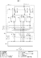
- FIG. 7 is a circuit diagram illustrating configurations of the pixel storage element Mx (i, j), the column selection circuit 162, and the signal processing circuit DS in the signal storage processing unit 155.
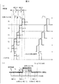
- FIG. 8A is a timing chart showing the drive timing of the pixel storage element Mx (i, j)
- FIG. 8B is a waveform diagram showing the reflected pulse light in an enlarged manner.
- the pixel storage element Mx (i, j) has a plurality of binary counters BC1 to BC ⁇ , a time switch 210, and an output switch 211.
- the binary counters BC1 to BC ⁇ are described as a representative, they are referred to as a binary counter BC ⁇ .
- the time switch 210 is a circuit including switches S1 to S ⁇ that selectively connect the signal line Lx (i, j) to the binary counters BC1 to BC ⁇ .
- the switches S1 to S ⁇ are composed of NMOS transistors. In the following description, when the switches S1 to S ⁇ are described as a representative, they are referred to as a switch S ⁇ .
- Binary counters BC1 to BC ⁇ are counters that count the pulse of the pixel signal from the pixel Px (i, j) input via the switches S1 to S ⁇ , respectively.
- the above pulses are input to the clock terminals of the binary counters BC1 to BC ⁇ .
- the reset signal Rf is input to the reset terminals R of the binary counters BC1 to BC ⁇ .
- the binary counters BC1 to BC ⁇ have output terminals of g1 bit, g2 bit,..., G ⁇ bit, respectively.
- the output switch 211 outputs the output of the binary counter BC ⁇ as a column signal when selected by the row selection signal line R ⁇ (j) (row selection signal lines R1 (j), R2 (j),..., R ⁇ 2 (j)).
- the output switch 211 is configured by an NMOS transistor having a gate connected to the row selection signal line R ⁇ (j), but is not limited thereto.
- One terminal of each NMOS transistor of the output switch 211 is connected to the output terminal of each bit of the binary counter BC ⁇ , and the other terminal is connected to the column signal line C (j).
- the binary counter BC ⁇ is connected to the signal line Lx (i, j) and accumulates the number of pulses transmitted from the pixel Px (i, j) for the time width ⁇ T ⁇ during which the switch S ⁇ is on.
- the output bit number g ⁇ of the binary counter BC ⁇ is determined by the maximum value of the number of photons to be measured.
- the column selection circuit 162 is a circuit that connects the column signal line C (j) to the signal processing circuit DS when selected by the column selection signal line CS (j).
- the NMOS transistor has a gate connected to the column selection signal line CS (j), but the present invention is not limited to this.
- the column selection circuit 162 connects column signal lines C (j + 1), C (j ⁇ 1) and the like arranged in parallel to the signal processing circuit DS.
- the reading order of the above-described integrated value of the number of photons from the pixel storage element Mx (i, j) is determined by selecting the output switch 211 by the row selection signal line R ⁇ (j) and each column signal line C by the column selection circuit 162. It is defined by the connection order of (j).
- the signal processing circuit DS can read the output of the binary counter BC ⁇ through the output switch 211 and the column signal line C (j) of the column selection circuit 162 even during integration by the binary counter BC ⁇ .
- the signals T1 to T ⁇ for driving the time switch 210 are signals for sequentially turning on the switches S1 to S ⁇ in time series as shown in FIG.
- the time widths ⁇ T1 to ⁇ T ⁇ for turning on the switches S1 to S ⁇ are equal to the half-value width ⁇ T of the pulsed light.
- the binary counters BC1 to BC ⁇ respectively count pulses and integrate the number of photons for each time period determined by the time widths ⁇ T1 to ⁇ T ⁇ .
- the binary counter BC1 measures the background light intensity. Therefore, the time width ⁇ T1 during which the switch S1 is turned on does not have to be the same as the on time ⁇ T ⁇ of the other switches S ⁇ .
- the noise level of the binary counter BC1 can be reduced by setting the length of the switch multiple times as long as the other switches S ⁇ are turned on. In that case, in the signal processing circuit DS, only the output value of the binary counter BC1 is divided by a multiple obtained by dividing the ON time length with respect to the other switch S ⁇ , and converted to data with the same time length as the other binary counter BC ⁇ . The trouble to do increases.
- the time widths ⁇ T2 to ⁇ T ⁇ are preferably equal to or less than the half-value width ⁇ T. Thereby, the influence of background light can be weakened and the signal-to-noise ratio of the signal can be improved.
- the time widths ⁇ T2 to ⁇ T ⁇ are longer than the half-value width ⁇ T, the influence of background light becomes strong, and the signal-to-noise ratio of the signal decreases.
- the time widths ⁇ T2 to ⁇ T ⁇ are twice as long as the half-value width ⁇ T, the background light measurement time is doubled with respect to the time during which the reflected light of the pulse light may be detected.
- the intensity ratio of the reflected pulse light to the background light is 1 ⁇ 2 compared to when the time width ⁇ T2 to ⁇ T ⁇ is substantially the same as the half-value width ⁇ T. Therefore, the detection sensitivity is deteriorated with respect to the far object 11 whose reflected light of the pulsed light is weaker than the background light.
- the binary counter BC2 receives the pulsed light reflected in an extremely short time as a light reception signal. That is, when the object 11 is located very close to the three-dimensional image element 153, the count number of the binary counter BC2 increases with respect to the count number of the binary counter BC1. With respect to the distance L between the object 11 and the three-dimensional image element 153, the reflected light of the pulsed light reaches the three-dimensional image element 153 after 2L / c (c: speed of light). A light reception signal having an intensity higher than that of the background light is input to the binary counter (the binary counters BC3 and BC4 in the example of FIG. 8A).
- the above integration is executed for a plurality of pulsed light emitted during one frame (for example, 1/30 sec). That is, a series of integrated values arranged in a time series acquired by the three-dimensional image element every time a plurality of times of pulsed light irradiation are integrated with each other.
- the data stored in each binary counter BC ⁇ is read out to the signal processing circuit DS, and then activated by the reset signal Rf, the count number up to that point is cleared, and the next frame is cleared. Ready to start measuring.
- the binary counter total number ⁇ has the following relationship with respect to the maximum measurement distance Dmax and the half-value width ⁇ T.
- the distance measurement accuracy can be improved by reducing the half-value width ⁇ T and increasing the total number of binary counters ⁇ .
- the binary counter total number ⁇ increases, the area of the pixel storage element Mx (i, j) increases, leading to an increase in the area of the chip constituting the three-dimensional image element 153 and an increase in the cost of the optical radar device 100. .
- the pixel storage element Mx (i, j) and the signal processing circuit DS are basically logic circuits, the area can be reduced by adopting a silicon LSI manufacturing process that has been miniaturized. Since the manufacturing cost of such a miniaturization process is decreasing year by year, the total number of binary counters ⁇ can be increased from tens to hundreds in the future.
- the signals T1 to T ⁇ do not overlap each other in principle and cover the time zone to be measured without omission, but in FIG. Since the processing can be simplified, the pulse widths to be activated are made equal to each other. However, the pulse widths to be activated are not necessarily limited to the case where they are equal to each other. For example, in order to improve the distance measurement accuracy for a short distance, the pulse width can be shortened at the first part of the lapse of time, and gradually increased with the lapse of time, or can be changed in a plurality of stages.
- the signals T1 to T ⁇ must be distributed to all the pixel storage elements Mx (i, j), there is a possibility that a slight error may occur in the wiring delay due to the variation in the delay between the wirings. Since the error in the pulse width for activating the signals T1 to T ⁇ is directly related to the accuracy of the distance measurement value, it is necessary to adopt a circuit configuration and wiring arrangement with high time accuracy according to the accuracy required for the optical radar device 100. There is.
- the switches S1 to S ⁇ constituting the time switch 210 are directly turned on / off by the signals T1 to T ⁇ in the example shown in FIG. 7, but may be configured by other circuits.
- a configuration in which each output of a simple shift register (the number of bits; ⁇ ) is connected to the switches S1 to S ⁇ and the ON state is sequentially shifted by a clock signal may be employed.
- the number of signals can be reduced, and only one of the switches S1 to S ⁇ can be reliably turned on. Therefore, for the switch S ⁇ and the switch S ( ⁇ + 1) that are adjacent to each other in the ON time zone, the counting error can be reduced by preventing the opening of the ON time zone or the occurrence of overlap.
- the time switch 210 may have any configuration as long as it is a circuit in which the opening time or overlap between adjacent switches is small.
- the binary counter BC ⁇ is used as a circuit for counting the pulse signal generated when the light receiving unit 154 detects photons in time series. This is because the binary counter BC ⁇ can be configured with a relatively simple circuit, and when configured as an integrated circuit, a function of counting and integrating with a small area can be realized. Another reason is that since the binary counter BC ⁇ is a simple logic circuit, it is easy to obtain a wide operation margin and the design is easy.
- the binary counter BC ⁇ has such advantages, but the pixel storage element Mx (i, j) does not necessarily need to be configured by a plurality of binary counters BC1 to BC ⁇ .
- any other configuration may be used as long as it is a circuit that integrates and stores the number of detected photons for each of a series of time intervals arranged almost continuously in time series in combination with the time switch 210. Further, it is preferable that the integration result during the integration can be read without greatly affecting the integration operation.
- the count number NC ⁇ (t) of pulses by each binary counter BC ⁇ at a certain time t is a count number NC1 (t), NC2 (T) and NC5 (t) are substantially equal values except for noise, and both represent the background light intensity.
- the count numbers NC3 (t) and NC4 (t) include the reflected light of the pulse light and are significantly larger than the count numbers NC1 (t), NC2 (t), and NC5 (t). Accordingly, the distance between the light receiving unit 154 and the object 11 is calculated by the following equation.
- the integer 8B it is “1”. However, the above number is an integer greater than or equal to 0. If the object is at a long distance, the integer increases, and decreases at a short distance.
- A is an integrated value of the reflected pulse light intensity measured during the timing T3
- B is an integrated value of the reflected pulse light intensity measured during the timing T4. Since the pulse width of the pulsed light and the time length to be measured are the same, as shown in FIG. 8B, the reflected light is detected only in at most two adjacent sections. Therefore, the length of the period Tb is similarly calculated from the intensity of the reflected light of the pulse light regardless of the distance of the object. Also, the above equation is divided by 2 because light travels back and forth between the object 11 and the object Ta 11 in a period that combines the period Ta and the period Tb, so that the distance to the object 11 is divided by 2. It is necessary.
- the signal processing circuit DS can output D (t) as the distance signal D (i, j) to each pixel Px (i, j).
- the signal processing circuit DS can output the following information as the two-dimensional image information G1 (i, j), G2 (i, j).
- G1 (i, j) NC1 (t)
- an integrated value larger than the noise level is obtained from the pulse count number NC ⁇ (t)
- a pair of the obtained integrated value and the integrated value temporally adjacent to each other is obtained, and the count number is obtained.
- the distance to the object can be calculated with an accuracy shorter than the time interval.
- the flight time with an accuracy of c ⁇ ⁇ T / 2 or less is obtained. It becomes possible to determine (the part other than the integer in [] of D (t)), and the distance measurement accuracy to the object can be improved.
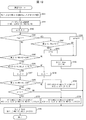
- FIG. 9 is a flowchart showing a procedure of signal processing by the signal processing circuit DS.
- the signal processing circuit DS may serially process the output signal of each pixel Px (i, j), or may have a plurality of arithmetic circuits and process the output signal of each pixel Px (i, j) in parallel. You may do it.
- the signal processing circuit DS reads the count numbers NC1 (t) to NC ⁇ (t) from the pixel storage element Mx (i, j), and stores them in the memory in the signal processing circuit DS (step S221).
- the signal processing circuit DS determines the noise level ⁇ N (t) (step S222).
- there are various noises such as dark current noise, 1 / f noise, thermal noise, etc., but the largest noise in the photon quantity measurement is shot noise.
- shot noise proportional to ⁇ N is attached to the number of detected photons N (average value).
- the count number NC ⁇ (t) must be considered to have noise proportional to ⁇ NC ⁇ (t).
- a ⁇ N (t) A ⁇ ⁇ NC1 (t) + B (B is a constant)
- A is preferably 3 or more, and more preferably 4 or more.
- B is a noise component other than shot noise, such as dark current noise.
- the count number NC1 (t) that does not include the reflected light of the pulse light and includes only the background light signal is used.
- the noise level ⁇ N (t) is determined by other methods. You may decide. For example, the count number NC ⁇ (t) is measured from the count number NC2 (t) without measuring the count number NC1 (t), and the average value Ave (NC ⁇ ) of the count number NC ⁇ (t) from the count number NC2 (t) Based on (t)), the calculation may be performed based on the following equation.
- ⁇ N (t) A ⁇ ⁇ Ave (NC ⁇ (t)) + B
- Ave (NC ⁇ (t)) is very close to the average value of background light.
- Ave (NC ⁇ (t)) decreases.
- NC ⁇ (t) In calculating the average value of NC ⁇ (t), some average values may be used instead of all the average values from NC2 to NC ⁇ . Further, when obtaining ⁇ N (t) using Ave (NC ⁇ (t)), BC1 for obtaining NC1 (t) can be omitted.
- the circuit scale increases and the calculation time becomes long. Therefore, an approximate value can be used instead.
- the noise level ⁇ N (t) when the most significant bit of the count number NC1 (t) is in the k-th digit, the number having the most significant bit in the k / 2 digit (rounded up when k is an odd number) is defined as the noise level ⁇ N (t).
- an approximation method is used such that a noise level ⁇ N (t) is a number having the most significant bit in the k / 2 digit (rounded up when k is an odd number) and the lower order bit is 1. It is also possible.
- step S223 a loop process for searching for an item significantly larger than the count number NC1 (t) from the count number NC2 (t) to the count number NC ⁇ (t) is executed (steps S223 to S226).
- the signal processing circuit DS sets the initial value of ⁇ to, for example, 2 at the beginning of this loop processing (step S223), and then determines whether ⁇ is equal to or less than the total binary counter ⁇ (step S224).
- step S224 when the signal processing circuit DS determines that ⁇ is equal to or smaller than the binary counter total number ⁇ (YES in step S224), the signal processing circuit DS determines whether or not the condition represented by the following equation is satisfied for ⁇ (step S224). Step S225).
- step S224 when the signal processing circuit DS determines that the condition represented by the above expression is satisfied for the above ⁇ (YES in step S225), ⁇ at that time is set to ⁇ (step S226). On the other hand, when the signal processing circuit DS determines in step S224 that the condition represented by the above expression is not satisfied for the above ⁇ (NO in step S225), 1 is added to ⁇ at that time (step S225). S227) The process returns to step S224.
- the count number NC ⁇ (t) is an integrated value larger than the noise level, and the count number NC ( ⁇ + 1) (t) is an integrated value that is temporally adjacent. A pair of count number NC ⁇ (t) and count number NC ( ⁇ + 1) (t) is extracted.
- the signal processing circuit DS calculates the measurement result according to the following equation when ⁇ is determined (step S228).
- IC (t) NC ⁇ (t) + NC ( ⁇ + 1) (t) ⁇ 2 ⁇ NC1 (t)
- D (t) c ⁇ ⁇ T ⁇ [( ⁇ 2) + ⁇ NC ( ⁇ + 1) (t) ⁇ NC1 (t) ⁇ / IC (t)] / 2
- the signal processing circuit DS obtains the next distance information D (i, j) and two-dimensional image information G1 (i, j), G2 (i, j) based on the result of the above calculation (step S229).
- the signal processing circuit DS stores the calculated distance information D (i, j) and the two-dimensional image information G1 (i, j), G2 (i, j) in a memory and outputs them to the external system 300 as appropriate.
- the signal processing circuit DS calculates and stores the distance information D (i, j) and the two-dimensional image information G1 (i, j), G2 (i, j) and stores them in the external system 300. Output.
- the specific calculation method of the distance information D (i, j) and the two-dimensional image information G1 (i, j), G2 (i, j) by the signal processing circuit DS is not limited to this, and various algorithms are adopted. Is possible.
- the SNR can be improved and the distance information can be obtained by integrating the measurement results (number of photons) of many laser pulse lights by the binary counter BC ⁇ .
- the intensity of the background light is 100
- the intensity of the reflected light of the pulsed light is 10
- the intensity of the reflected light is almost the same as the noise of the background light and cannot be reliably detected by one measurement.
- the measurement results of 100 times are integrated, the intensity of the background light is 10,000 and the shot noise is on the order of 100.
- the intensity of the reflected light of the pulsed light is 1000, which is an order of magnitude larger than the noise of the background light, and is a value that can be reliably detected.
- a mechanism for performing this integration digitally and in parallel for all the pixels Px (i, j) can be realized with silicon. Therefore, even in an environment with strong background light, the optical radar device 100 that extends the distance measurement range can be provided at a low cost.
- the pixel storage element Mx (i, j) of the present embodiment has a function in which the binary counter BC ⁇ counts the number of photons detected as electric pulses by the pixel Px (i, j), and the signal processing circuit DS The function of reading the count result can be executed in parallel. As a result, the measurement result cannot be taken out until one frame is completed, and the measurement result can be taken out even in the middle of one frame.
- the frame frequency is 30 Hz
- 1/30 (second) time can be used to acquire one frame of data
- the object 11 is located at a short distance, data may be obtained even with one pulse emission.
- the far object 11 cannot obtain data unless a large number of pulse emission data are accumulated.
- information on the object 11 close to the optical radar device 100 can be output earlier by obtaining an intermediate measurement result.
- collisions can be prevented by detecting an object closest to a car or robot on which the optical radar device 100 is mounted as early as 1/30 (second) and issuing an alarm to a control system of the car, robot, or the like.
- the relative speed with the object 11 in a short distance of several meters reaches 100 km / h. If the speed is 30 km / h, the distance moved in 1/30 (second) is about 30 cm, and the time is short. However, the possibility of avoiding a collision can be increased.
- the two-dimensional image information G1 (i, j) is information based on background light and is useful for recognizing the shape and the like of the object 11. It is. In particular, when information from a normal image sensor is used together, the information is compared with the two-dimensional image information G1 (i, j), and the object 11 common to both is specified. Recognition of the object 11 and acquisition of the distance between the object 11 and the light receiving unit 154 can be performed. Furthermore, when it is difficult to specify the distance due to a large error, the approach of the object 11 can be determined by capturing the time passage of the two-dimensional image information G2 (i, j).
- the two-dimensional image information G2 (i, j) may be compared between consecutive frames or between distant frames, or may be compared for each of a plurality or a single pulse emission.
- the signal processing circuit DS reads the count number of the number of photons for the pixel Px (i, j) of M rows and N columns in any order, and the distance information D (i, j) and two-dimensional based on the count number You may control the procedure of calculating image information G1 (i, j), G2 (i, j). Further, the signal processing circuit DS may have a memory used for the control. Further, the signal processing circuit DS may control the timing for counting the photon detection signal of the pixel Px (i, j). This control is, for example, a control in which the activation time of the signal T1 shown in FIG. 8 is made several times the activation time of the other signal T ⁇ in order to measure the background light signal with high accuracy.
- the signal processing circuit DS may control the timing for generating the pulsed light, or may control the timing for activating the pixel Px (i, j). For example, the signal processing circuit DS activates the pixel Px (i, j) to measure the above-described background light, stores the count number in BC1 during the time width ⁇ T1, and the time of the time width ⁇ T1 has elapsed. At that time, a signal is emitted to the pulsed light illumination system 110 via the control element 160 so that the pulsed light is emitted. Thus, the signal T2 is activated when the time width ⁇ T1 has elapsed.
- the signal storage processing unit 155 or the control element 160 has a memory for storing at least distance information D (i, j) and two-dimensional image information G1 (i, j) and G2 (i, j) information of all pixels. May be.
- the signal processing circuit DS may sequentially store the obtained information in this memory, and may output the information to the external system 300 via the control element 160 in response to a request from the external system 300. Further, when the signal processing circuit DS has memories for a plurality of frames, the signal processing circuit DS may further output the results of comparison and calculation between the frames.
- ⁇ Effect verification> A prototype was produced based on the above embodiment, and its characteristics were evaluated.
- the pulsed light illumination system 110 three VCSELs having a peak wavelength of 945 nm were used as the light emitting elements 122, and each pulse peak output was set to 25 W, and the pulsed light illumination system 110 was driven to emit light with a pulse half width of 100 nsec.
- the irradiation intensity at the center of the irradiation region was the highest at 12 ⁇ W / cm 2, the irradiation intensity at the four corners was the lowest, and the minimum was 10.6 ⁇ W / cm 2.
- the maximum and minimum values were within ⁇ 10% of the average value.
- the repetition emission frequency of the laser pulse was set to 19 kHz in consideration of class 1 conditions. Assuming image acquisition at 30 frames per second, data can be stored for a maximum of 633 laser pulse emissions per frame.
- the imaging optical system 151 of the light receiving system 140 a lens having a focal length of 4.5 mm, an F number of 1.8, and an effective diameter of 2.5 mm was used.
- the optical bandpass filter 152 an interference filter was used in which the center wavelength was selected so that the peak wavelength of the laser coincided with the center value of the transmission band at room temperature.
- the interference filter was coated on the inside of a lid glass 171 that hermetically seals a package 170 that houses the three-dimensional image element 153. Nitrogen having a low dew point was used as the atmosphere 172 in the package.
- the half band width of the transmission band of the interference filter was 10 nm, and the average transmittance was 55%. Since the temperature dependency of the emission peak wavelength of VCSEL is 0.07 nm / K and the center value of the transmission band of the interference filter is 0.025 nm / K, the relative value of the laser peak wavelength and the center value of the interference filter transmission band is The deviation was ⁇ 2.8 nm between 85 ° C. and ⁇ 40 ° C. This deviation is within the transmission band width of 10 nm even when the half-value width of 1 nm of the laser emission peak is included, and the VCSEL can be used without any temperature control. It is important to match the emission peak wavelength of the light emitting element 122 with the transmission band center value of the optical bandpass filter 152 near the temperature located in the center of the temperature band to be used.
- the light receiving unit 154 of the three-dimensional image element 153 50 ⁇ m square pixels Px (i, j) are arranged such that 180 effective pixels in the horizontal direction and 40 effective pixels in the vertical direction are arranged. It was composed of a total of 7.2k effective pixels.
- each SPAD 180 is provided with a microlens 181 having a base size of 15 ⁇ m.
- the height of the microlens was about 10 ⁇ m.
- the fill factor of this pixel Px (i, j) was 22%.
- Each SPAD 180 was operated with a deadtime Td of 20 nsec.
- the effective quantum efficiency of SPAD180 having this microlens 181 was 10%.
- the number of photons received by the background light measured on a white plate with a reflectance of 50% with respect to 945 nm infrared light at noon in fine weather was 0.29 per SPAn180 and 100 nsec on average. Therefore, the average number of photons detected from the background light of all seven SPADs was 1.9 per 100 nsec.
- counting with a pulse of a 1.0 nsec width pixel signal a plurality of photons are detected almost simultaneously, and there is a possibility of undercounting about 2%, but this is not a numerical value that greatly affects the count result.
- the signal storage processing unit 155 when the signal storage processing unit 155 is arranged on one side of the light receiving unit 154, it is necessary to arrange at least 40 wires in a width of 50 ⁇ m. If the wiring is arranged at a pitch of 1 ⁇ m, a single-layer wiring can be realized. However, since a power supply line and other wirings are also necessary, the signal line Lx (i, j) is configured by two layers of the upper-layer wiring.
- the wiring delay time becomes the drive capability rate limiting of the signal line drive circuit 197 that charges the parasitic capacitance of the signal line Lx (i, j).
- the area that can be used for the signal line drive circuit 197 is limited, and a delay time of about several hundred psec occurs. Therefore, the delay time of the delay circuit 194 of the photon detection signal generator 191 shown in FIG. 6 is set to 500 psec. On the other hand, the delay time of the delay circuit 199 of the pixel signal output circuit 196 is set to 700 psec.
- the image storage element Mx (i, j) shown in FIG. 7 has four binary counters BC1 to BC4.
- the binary counters BC1 and BC4 are 12-bit binary counters
- the binary counter BC2 is a 16-bit binary counter
- the binary counter BC3 is a 13-bit binary counter.
- the number of bits is increased because there is a possibility that the count number may be increased by receiving strong laser pulse reflected light from the object 11 with a short distance from the three-dimensional image element 153.
- the row selection circuit 161 sequentially selects the row selection signal lines R1 (i), R2 (i), R3 (i), and R4 (i) for each row.
- the output switch 211 outputs the output data of the corresponding binary counters BC1, BC2, BC3, and BC4, respectively.
- the signal processing circuit DS has only one arithmetic circuit in order to reduce the circuit scale.
- the signal processing circuit DS is composed of a memory for temporarily storing data of the binary counters BC1 to BC4, a 16-bit microcomputer for executing a distance calculation, and the like.
- the algorithm used for distance extraction can be changed by using a microcomputer.
- a microcomputer with a bit number (in this case, 16 bits) that is greater than or equal to the maximum number of bits of the binary counters BC1 to BC4
- the speed of distance extraction can be improved, and the time between pulse emission (about 50 ⁇ sec) Distance extraction for all pixels is possible.
- the design period is shortened, but the area of the signal processing circuit DS is increased and the cost is increased.
- a dedicated circuit can be designed.
- the signal processing circuit DS can program in what order the pixel storage elements Mx (i, j) are processed using the function of the microcomputer.
- the pixel storage elements Mx (i, j) are processed using the function of the microcomputer.
- the optical radar device 100 used for monitoring the surroundings of an automobile, normally there is a higher possibility that an obstacle appears at the lower end than at the upper end of the field of view. In this case, it is preferable to process from the lower part of the visual field to the upper part.
- an obstacle can be detected earlier by checking from the left end of the field of view when the vehicle moves backward.
- the vicinity of the person can be intensively checked.
- the signal processing circuit DS has a memory (230 kb) having a capacity of 32 bits for each pixel Px (i, j). This memory accumulates the two-dimensional image information G2 (i, J) between frames, thereby improving the accuracy of distance information, storing the integrated value, and comparing it with another measured value or integrated value. By doing so, it is possible to detect approach and departure.
- the signal processing circuit DS When the signal processing circuit DS is laid out by a process of 0.13 ⁇ m, the area of the signal processing circuit DS is 2 mm ⁇ 2 mm, and the area of the pixel storage element Mx (i, j) is 50 ⁇ m ⁇ 20 ⁇ m. The size of 153 was 10 mm ⁇ 5.5 mm.
- the signal processing circuit DS also includes a non-volatile memory for storing operation conditions such as a distance extraction algorithm and a scanning order of the pixel storage element Mx (i, j).
- a white plate having a reflectance of 50% with respect to 945 nm infrared light was used as the object 11, and pulsed light was examined in a measurable range under three conditions: clear sky, cloudy, and nighttime.
- the average count values of binary counters BC1, BC2, BC3, and BC4 obtained by one-time pulse light irradiation are 1.9, 7.5, and 2.0 at a distance of 2 m, respectively. 1.9, and it was possible to capture the presence of the object 11 in the vicinity. As a result, the object 11 up to 3.5 m could be detected. Therefore, it is possible to capture where the nearest object 11 is in this way from the measurement result of one pulsed light, and transmit the result to the external system 300.
- the difference between the binary counter BC3 and the binary counter BC1 is an error range in one measurement, and the distance between the light receiving unit 154 and the object 11 cannot be specified.
- the distance increases when the count number of the binary counter BC2 corresponding to the same pixel Px (i, j) increases. It can be judged that it is approaching and is moving away when it decreases. Based on such determination, it is useful to output the pulsed light reflection intensity for each frame.
- the three-dimensional image element 153 of this embodiment can collect the surrounding three-dimensional information including distance information. it can.
- Embodiment 2 The following describes Embodiment 2 of the present invention with reference to FIG.
- FIG. 10 is a flowchart showing a signal processing procedure by the signal processing circuit DS in the three-dimensional image element 153 of the optical radar device 100 according to the present embodiment.
- the optical radar device 100 according to the present embodiment is the same as that of the first embodiment except that the distance extraction algorithm of the signal processing circuit DS is different from that of the first embodiment.
- the distance extraction algorithm of the first embodiment is simple, but the difference between the count number NC ⁇ (t) and the count number NC1 (t) is small, or the difference between NC ( ⁇ + 1) (t) and NC1 (t) is If it is small, it is susceptible to measurement errors. The algorithm described below improves this point.
- FIG. 10 is a schematic diagram showing a procedure of signal processing by the signal processing circuit DS in the three-dimensional image element 153 of the optical radar device 100 according to the present embodiment.
- the signal processing circuit DS first performs the processes of steps S221 and S222 shown in FIG. 9, and then executes a loop process for searching for the maximum value of NC ⁇ (t) (steps S240 to S243). .
- the signal processing circuit DS sets the initial value of ⁇ to 2, for example, and sets the initial value of ⁇ to 1 (step S240).
- ⁇ is equal to or less than the total number of binary counters ⁇ . Whether or not (step S241).
- step S241 when the signal processing circuit DS determines that ⁇ is equal to or smaller than the total number of binary counters ⁇ (YES in step S241), it is determined whether or not ⁇ and ⁇ satisfy the condition represented by the following expression. Determination is made (step S242).
- step S242 when the signal processing circuit DS determines that the above-described conditions for ⁇ and ⁇ are satisfied (YES in step S242), ⁇ at that time is set to ⁇ (step S243). . On the other hand, when the signal processing circuit DS determines in step S242 that the above-described conditions for ⁇ and ⁇ are not satisfied (NO in step S242), the value of ⁇ is not changed. In either case (YES and NO in step S242), 1 is added to ⁇ at that time (step S244), and the process returns to step S241.
- step S241 when the signal processing circuit DS determines that ⁇ exceeds the binary counter total number ⁇ (NO in step S241), the maximum value of NC ⁇ (t) is determined and the value of ⁇ is also determined. .
- the signal processing circuit DS determines whether or not ⁇ satisfies the condition expressed by the following equation, that is, the difference between the count number NC ⁇ (t) and the count number NC1 (t) is a noise level ⁇ N. It is determined whether it is larger (step S245).
- step S245 when the signal processing circuit DS determines that the above ⁇ satisfies the condition expressed by the above equation (YES in step S245), the count number NC ⁇ (t) is significantly greater than the count number NC1 ( It can be said that it is larger than t). In this case, the signal processing circuit DS further determines whether or not the above ⁇ satisfies the condition expressed by the following equation (step S246).
- step S246 when the signal processing circuit DS determines that the condition represented by the above expression is satisfied for the above ⁇ (YES in step S246), ⁇ is set to ⁇ + 1 (step S247). In step S246, when the signal processing circuit DS determines that the condition represented by the above equation is not satisfied with respect to ⁇ (NO in step S246), ⁇ is set to ⁇ 1 (step S248).
- the signal processing circuit DS determines whether or not the condition represented by the following equation is satisfied with respect to ⁇ , that is, the difference between the count number NC ⁇ (t) and the count number NC1 (t). Is greater than the noise level ⁇ N (step S249).
- step S249 if the signal processing circuit DS determines that the above ⁇ does not satisfy the condition expressed by the above equation (NO in step S245), the count number NC ⁇ (t) is significantly greater than the count number NC1 ( It cannot be said that it is larger than t). In this case, when ⁇ and ⁇ are determined, the signal processing circuit DS calculates the measurement result according to the following equation (step S250).
- the signal processing circuit DS obtains the next distance information D (i, j) and two-dimensional image information G1 (i, j), G2 (i, j) based on the result of the above calculation (step S251).
- the signal processing circuit DS stores the calculated distance information D (i, j) and the two-dimensional image information G1 (i, j), G2 (i, j) in a memory and outputs them to the external system 300 as appropriate.
- step S249 if the signal processing circuit DS determines that the above condition is satisfied (YES in step S249), it can be said that the count number NC ⁇ (t) is significantly larger than the count number NC1 (t). In this case, the signal processing circuit DS determines whether or not ⁇ is smaller than ⁇ (step S252).
- step S252 when the signal processing circuit DS determines that ⁇ is smaller than ⁇ , the signal processing circuit DS calculates the measurement result according to the following equation (step S253), and the process proceeds to step S251.
- step S252 NC ⁇ (t) + NC ⁇ (t) ⁇ 2 ⁇ NC1 (t)
- D (t) c ⁇ ⁇ T ⁇ [( ⁇ 2) + ⁇ NC ⁇ (t) ⁇ NC1 (t) ⁇ / IC (t)] / 2 If the signal processing circuit DS determines in step S252 that ⁇ is not smaller than ⁇ ( ⁇ is greater than or equal to ⁇ ), the signal processing circuit DS calculates the measurement result according to the following equation (step S254), and the process proceeds to step S251. To do.
- the signal processing circuit DS calculates and stores the distance information D (i, j) and the two-dimensional image information G1 (i, j), G2 (i, j) and stores them in the external system 300. Output.
- the distance and the like are calculated by the equations of steps S253 and S254, respectively, according to the magnitude relationship between ⁇ and ⁇ (step S252). Thereby, the distance with the highest accuracy can be obtained.
- FIG. 11 is a block diagram showing a configuration of the three-dimensional image element 153 constituting the optical radar device 100 according to the present embodiment.
- the essential difference between the present embodiment and the first embodiment is that the maximum number of binary counters BC ⁇ constituting the pixel memory element Mx (i, j) is increased to 21.
- the algorithm of Embodiment 2 was used for the distance estimation algorithm. The details will be described below.
- the three-dimensional image element 153 includes divided signal storage processing units 155a and 155b.
- the signal storage processing units 155a and 155b are arranged on both sides of the light receiving unit 154, the signal storage processing unit 155a is arranged on the lower side in the drawing, and the signal storage processing unit 155b is arranged on the upper side in the drawing.
- the light receiving unit 154 is not essentially changed from the light receiving unit 154 in the first embodiment.
- the signal storage processing unit 155a performs signal processing of 20 rows of pixels Px (i, j) located in the half of the signal storage processing unit 155a side in the light receiving unit 154.
- the signal storage processing unit 155b performs signal processing of 20 rows of pixels Px (i, j) located in the half of the signal storage processing unit 155b side in the light receiving unit 154.
- the number of bits of the binary counter BC ⁇ is changed for each binary counter from 16 bits to 12 bits in consideration of the maximum signal value that can be counted by each binary counter BC ⁇ .
- the numbers of bits of the binary counters BC1, BC2, BC3, BC4, and BC5 are 16 bits, 17 bits, 15 bits, 14 bits, and 13 bits, respectively.
- the number of bits of the binary counters BC6 to BC22 is 12 bits.
- the number of binary counters BC1 to BC21 increases greatly, the number of transistors constituting the time switch 210 connected to the signal line Lx (i, j) increases. As a result, the load on the signal line Lx (i, j) increases and the signal delay may increase, so a buffer is added at the forefront of the time switch 210. This is because the area of the pixel memory element Mx (i, j) is increased, and thus the wiring length of the signal line Lx (i, j) is increased.
- the signal storage processing units 155a and 155b have row selection circuits 161a and 161b, column selection circuits 162a and 162b, column signal lines Ca (j) and Cb (j), and signal processing circuits DSa and DSb, respectively. is doing.
- the signal processing circuits DSa and DSb each have the same capability for data processing because the amount of data to be handled increases. Therefore, the signal storage processing units 155a and 155b can perform data processing of the respective areas in parallel.
- the signal processing circuits DSa and DSb each have one arithmetic circuit. However, laser light emission timing control, pixel Px (i, j) activation timing control, signal readout from pixels Px (i, j) of M rows and N columns (array), calculation procedure control, memory Only the signal processing circuit DSa has functions such as management and output control.
- the three-dimensional image device 153 identified the object 11 up to 19 m under the maximum integration condition of a 1/30 sec frame period in the daytime in fine weather.
- the maximum measurement error at a distance in the range of more than 6 m and 19 m or less was 1 m.
- the maximum measurement error at a distance in the range of 6 m or less and 1 m or more was 0.31 m. For distance measurement exceeding 9 m, it was difficult in Embodiment 1 to refer to the time change of IC (t), but in this embodiment, it can be measured up to 19 m although there is an error.
- the measurement accuracy by the three-dimensional image element 153 of the present embodiment is improved even in cloudy weather and at night.
- the three-dimensional image element 153 recognizes the object 11 that is separated up to 30 m, and the maximum distance measurement error up to 30 m is 0.5 m.
- the three-dimensional image element 153 recognizes the object 11 separated to a distance of 30 m, and the maximum measurement error is 0.3 m.
- the object 11 up to 3 m was captured by accumulating 10 pulsed emissions, and the distance could be measured with a maximum error of 0.5 m.
- accumulation of signals in the pixel storage element Mx (i, j) by 100 pulses could be measured with a maximum error of 0.27 m within a distance of 3 m.
- the distance measurement is difficult, but in the present embodiment, it is improved so that the distance can be measured in a short time while being rough.
- Embodiment 4 The following describes Embodiment 4 of the present invention.
- This embodiment is different from the third embodiment in the following points, but other than that is basically unchanged from the third embodiment.
- the number of bits of the binary counter BC ⁇ constituting the pixel storage element Mx (i, j) is unified to 12 bits for all the binary counters BC ⁇ to facilitate the design.
- the memory (230 kb) having a capacity of 32 bits for each pixel Px (i, j) included in the signal processing circuit DS described in the first embodiment may be diverted to the present embodiment or newly added to each pixel.
- a memory (86 kb) having a capacity of 12 bits may be added.
- 12 bits is a sufficient number of bits to describe a distance of up to 30 m as a 2-bit integer in centimeters.
- the function of the signal processing circuit DS shown in FIG. 3 and the signal processing circuits DSa and DSb shown in FIG. 11 may be realized by a logic circuit (hardware) formed in an integrated circuit (IC chip) or the like. As described above, the function may be realized by software using a microcomputer.
- the signal processing circuits DS, DSa, DSb can be read by a CPU (Central Processing Unit) that executes instructions of a program that is software that implements each function, and the program and various data can be read by a computer (or CPU). It includes a recorded ROM (Read Only Memory) or a storage device (these are referred to as “recording media”), a RAM (Random Access Memory) for expanding the program, and the like. And the objective of this invention is achieved when a computer (or CPU) reads the said program from the said recording medium and runs it.
- ROM Read Only Memory
- storage device these are referred to as “recording media”
- RAM Random Access Memory
- a “non-temporary tangible medium” such as a tape, a disk, a card, a semiconductor memory, a programmable logic circuit, or the like can be used.
- the program may be supplied to the computer via an arbitrary transmission medium (such as a communication network or a broadcast wave) that can transmit the program.
- an arbitrary transmission medium such as a communication network or a broadcast wave
- one embodiment of the present invention can also be realized in the form of a data signal embedded in a carrier wave, in which the program is embodied by electronic transmission.
- the three-dimensional image element includes a pixel Px (i, i, which includes an avalanche photodiode (SPAD180) that detects photons of incident light including reflected light from the object 11 to be detected in a Geiger mode. j) and a plurality of light receiving units 154 corresponding to the pixels Px (i, j) and output from the pixels Px (i, j) as photon detection results.
- a pixel Px i, i, which includes an avalanche photodiode (SPAD180) that detects photons of incident light including reflected light from the object 11 to be detected in a Geiger mode.
- a plurality of light receiving units 154 corresponding to the pixels Px (i, j) and output from the pixels Px (i, j) as photon detection results.
- a plurality of integration units (pixel storage elements Mx (i, j)) that integrate in a series of time intervals (time widths ⁇ T1 to ⁇ T ⁇ ) continuously arranged in the series, and the time series integrated by the integration unit
- a calculation unit that calculates distance information D (i, j) related to the distance between the light receiving unit 154 and the object 11 for each pixel Px (i, j) using a series of integrated value groups (count number NC ⁇ ). (Signal processing Is provided with a road-DS), the.
- the SN ratio can be improved and distance information can be obtained.
- the intensity of the reflected light from the object 11 is 10
- the pulse signals detected in 100 measurements are integrated, the intensity of the background light becomes 10,000 and the shot noise becomes 100.
- the intensity of the reflected light is 1000, which is one digit larger than the background light noise, and is a value that can be reliably detected.
- a three-dimensional image element is the aspect 1, wherein the calculation unit determines a noise level of the integrated value group based on the integrated value group, and the integrated value group includes the function A function for extracting an integrated value greater than the noise level, extracting a pair of integrated values that are temporally adjacent to the calculated integrated value, and determining the flight time of light from the extracted pair with an accuracy shorter than the time interval. It may have a function.
- the calculation unit reads out the integrated value from the integrating unit in parallel with the integration of the number of photons by the integrating unit. May be.
- the integrated value can be taken out even during the integration. Thereby, the distance information regarding the object close to the three-dimensional image element can be output earlier.
- the light receiving unit 154, the integrating unit, and the calculating unit may be formed monolithically on a silicon substrate.
- the three-dimensional image element can be provided at a lower cost.
- the pixel Px (i, j) may include a plurality of the avalanche photodiodes.
- the detection accuracy can be further increased.
- the three-dimensional image element according to Aspect 6 of the present invention is the Aspect 6 according to any one of Aspects 1 to 5, wherein the integration unit has a plurality of binary counters BC ⁇ for integrating the previous pulse signal for each time interval. It may be.
- the three-dimensional image element according to aspect 7 of the present invention is the switching circuit (column selection circuit 162) according to aspect 6, wherein the integrated value group from each binary counter BC ⁇ is switched for each binary counter BC ⁇ and output to the calculation unit.
- the number of signal lines that output the integrated value group from the switching circuit to the calculation unit may be equal to or greater than the maximum number of output bits of each binary counter BC ⁇ .
- the number of signal lines for outputting the integrated value is at least the maximum number of output bits of each binary counter. Just do it.
- the wiring structure of a binary counter and a calculation part can be simplified.
- the calculation unit reads out the integration value group from the integration unit according to a readout order stored in advance. May be.
- the integrated value can be read at an early stage from the integrating unit that integrates the number of photons obtained from the pixels that have detected the reflected light from the object close to the three-dimensional image element.
- the calculation unit may further calculate light intensity information representing the intensity of incident light using the integrated value group. good.
- the two-dimensional image of the object can be specified by the light intensity information.
- a three-dimensional image can be obtained by combining the light intensity information and the distance information.
- An optical radar device includes the light emitting element 122 that irradiates the target object to be detected with the pulsed light, and the three-dimensional image element 153 according to any one of the aspects 1 to 9, and the 3
- the avalanche photodiode in the dimensional image element 153 detects photons of the reflected light of the pulsed light with respect to the object 11.
- an inexpensive optical radar device with a wide measurement range can be provided.
- the optical radar device is the optical radar apparatus according to aspect 10, wherein the light emitting element emits pulsed light a plurality of times, and the integration unit of the three-dimensional image element performs irradiation of the pulsed light a plurality of times.
- a series of integrated value groups arranged in a time series acquired by the three-dimensional image element may be integrated with each other.
- the optical radar device is the optical radar device according to aspect 10 or 11, wherein the three-dimensional image element 153 includes the distance information regarding the distance to the object and the pulsed light emitted to the object 11.
- First light intensity information (two-dimensional image information G2 (i, j)) indicating the intensity of reflected light from the object 11, and second light intensity information not including the reflected light from the object 11 of the pulsed light. (Two-dimensional image information G1 (i, j)) may be output.
- the second light intensity information is information based on background light, and is useful for recognizing the shape of the object. Further, when it is difficult to specify the distance due to a large error, it is possible to determine the approach of the object by capturing the passage of time of the first light intensity information. For example, if the value of the first light intensity information increases significantly, the object approaches the pixel, and if the value of the first light intensity information decreases, the object moves away from the pixel. ing.
- the length of the time interval may be equal to or less than the half-value width of the pulsed light.
- An optical radar apparatus includes a light emitting element 122 that irradiates a target object to be detected with pulsed light, and the three-dimensional image element 153 according to aspect 6 or 7, and the three-dimensional image element.
- the avalanche photodiode at 153 detects photons of the reflected light of the pulsed light with respect to the object 11, and the binary counter BC ⁇ of a part of each integrating unit emits pulsed light that irradiates the object 11. Before, the number of photons of the incident light may be integrated.
- the calculation unit can obtain distance information in which the influence of the background light is suppressed by using the intensity of the background light.
Landscapes
- Engineering & Computer Science (AREA)
- Physics & Mathematics (AREA)
- General Physics & Mathematics (AREA)
- Radar, Positioning & Navigation (AREA)
- Remote Sensing (AREA)
- Computer Networks & Wireless Communication (AREA)
- Electromagnetism (AREA)
- Multimedia (AREA)
- Signal Processing (AREA)
- Optical Radar Systems And Details Thereof (AREA)
Abstract
【課題】広い測定範囲を有する安価な3次元画像素子を実現する。3次元画像素子(153)は、検出の対象となる対象物からの反射光を含む入射光のフォトンをガイガーモードで検出するSPAD(単光子雪崩増倍フォトダイオード)を含む画素(Px(i,j))を複数有する受光部(154)と、画素(Px(i,j))と一対一に対応して設けられ、画素(Px(i,j))からフォトンの検出結果として出力されるパルス状の画素信号を、時系列に連続して並んだ一連の時間区間毎に積算する複数の画素記憶素子(Mx(i,j))と、画素記憶素子(Mx(i,j))によって積算された時系列に並ぶ一連の積算値群を用いて、受光部(154)と対象物との距離に関する距離情報を画素毎(Px(i,j))に算出する信号処理回路(DS)とを備える。
Description
本発明は、対象物の2次元画像と対象物までの距離情報とからなる3次元画像を取得する3次元画像素子に関する。
3次元イメージは、通常の写真の様な2次元イメージに加えて、視野内の対象物までの距離情報も含めた概念である。近年、このような3次元イメージを検出する3次元イメージセンサは、自動車やロボット等の周辺認識に用いられるセンサとして極めて重要となっている。2次元イメージを検出する2次元イメージセンサとしては、CCDおよびCMOSイメージャが普及している。CCDおよびCMOSイメージャ、何れもシリコン製フォトダイオードによって光強度を電気信号に変換して画像化している。また、高精度の距離情報の計測は、レーザ光を対象物に照射して、対象物からレーザ光が反射して戻って来るまでの飛行時間(Time-of-flight)を計測する方法が普及しつつある。
視野全体にレーザ光を照射する方法としては、点状または帯状に絞ったレーザビームを、ミラー等によってスキャンするスキャンタイプと、視野全体にほぼ均一にレーザビームを広げて照射する一括照射タイプとが有る。このうち、非特許文献1に開示されているように、対象物上で強いビーム強度が得易いスキャンタイプが多く開発されている。スキャンタイプは、ビームを振る為の機械的な機構が必要となる為、高価で装置が大きくなる。一方、一括照射タイプは、スキャンする機械的な機構が必要無い為、小型化し易いが、対象物上でのレーザ光強度がスキャンタイプに比べて弱くなる為、対象物までの距離が長くなると、信号強度が弱くなって、距離測定精度が落ちる。
飛行時間計測に関しては、時間測定精度が距離精度に直結する為に、パルスレーザ光を複数回発射し、発光から受光までの時間測定を繰り返し、ヒストグラム(横軸:時間、縦軸:頻度)を構成し、飛行時間を決定する方法が有る。この手法は、TCSPC(Time-Correlated-Single-Photon-Counting:時間相関単光子数計測)と呼ばれる手法である。
受光素子としては、SPAD(Single-Photon-Avalanche-Diode:単光子雪崩増倍フォトダイオード)が用いられる。この受光素子は、例えば、特許文献2および非特許文献1に記載されているように、画素当たりの回路規模が大きい為、大規模な画素を2次元配列したイメージャでは用いられておらず、主にスキャンタイプと組合せて用いられている。
一方、一括照射タイプは、フォトダイオードの電流を計測し、判定値と比較して飛行時間を決定している。また、一括照射タイプでは、時系列に並べたキャパシタに順次、前記電流を蓄積し、その蓄積量で飛行時間を判定する場合も有る。この仕組みから、1回のレーザ照射で3次元イメージを構成することとなる為、写真で言えばフラッシュを当てて画像を撮った様に、視野全体に渡って同時性が確保される。このような一括照射タイプは、例えば、特許文献1および3に開示されているように、視野の各点毎に、時刻が異なるスキャンタイプとは大きく異なり、「フラッシュ」と形容されている。
Cristiano Niclass, Member, IEEE, Mineki Soga, Hiroyuki Matsubara, Masaru Ogawa, and Manabu Kagami, Member, IEEE, IEEE JOURNAL OF SOLID-STATECIRCUITS, VOL. 49, NO. 1, JANUARY 2014, P315-330 "A 0.18-μm CMOS SoC for a 100-m-Range 10-Frame/s 200×96-Pixel Time-of-Flight Depth Sensor."
しかしながら、上述した従来の技術では、以下の課題がある。
民生用の自動車、ロボット等に使用する為には、装置の小型化および耐久性が極めて重要であることから、スキャンタイプは好ましく無い。一方、一括照射タイプでは、背景光対策が問題となる。自動車用途では、光レーダー装置が赤道直下の真昼の強烈な太陽光の下でも動作せねばならない。特許文献1に開示されたセンサでは、日中の背景光の影響を最小限にする為、波長1.5μm程度の赤外光を使う都合上、シリコン型の受光素子を使用できず、InGaAs等の化合物半導体を使用しなければならない。一方、当該センサでは、シリコンLSIが信号処理を行う。この為、当該センサは、InGaAs製のフォトダイオードとシリコンLSIとを積層しなければならないので、材料および製造工程の面でコストが嵩むことにより非常に高価な装置となる。
そこで、受光から信号処理までの機能を同じシリコンチップに搭載し、安価で測定範囲が広い3次元画像素子と、これを用いた一括照射タイプの光レーダー装置が求められている。
本発明の一態様は、広い測定範囲を有する安価な3次元画像素子を実現することを目的とする。
上記の課題を解決するために、本発明の一態様に係る3次元画像素子は、検出の対象となる対象物からの反射光を含む入射光のフォトンをガイガーモードで検出するアバランシェフォトダイオードを含む画素を複数有する受光部と、前記画素と一対一に対応して設けられ、前記画素からフォトンの検出結果として出力されるパルス信号を、時系列に連続して並んだ一連の時間区間毎に積算する複数の積算部と、前記積算部によって積算された時系列に並ぶ一連の積算値群を用いて、前記受光部と前記対象物との距離に関する距離情報を前記画素毎に算出する算出部とを備えている。
本発明の一態様によれば、広い測定範囲を有する安価な3次元画像素子を実現することができるという効果を奏する。
本発明の実施形態について図1~図11に基づいて説明する。以下、説明の便宜上、特定の実施形態にて説明した構成要素と同一の機能を有する構成要素については、同一の符号を付記し、その説明を省略する場合がある。
〔実施形態1〕
本発明の実施形態1について図1~図9に基づいて説明すれば、以下の通りである。
本発明の実施形態1について図1~図9に基づいて説明すれば、以下の通りである。
図1は、本実施形態に係る光レーダー装置100の構成を示す模式図である。
〈光レーダー装置100の構成〉
図1に示す様に、光レーダー装置100は、対象視野10にパルス光124を照射するパルス光照明系110と、対象視野10の少なくとも一部からの光を受光する受光系140とを備えている。
図1に示す様に、光レーダー装置100は、対象視野10にパルス光124を照射するパルス光照明系110と、対象視野10の少なくとも一部からの光を受光する受光系140とを備えている。
パルス光照明系110は、照明系電源120と、発光素子駆動回路121と、拡散光学系123と、発光素子122とを有している。拡散光学系123は、発光素子122が発するパルス光124を対象視野10の全体に一括照射する。発光素子駆動回路121は、発光素子122をパルス駆動する回路である。照明系電源120は、発光素子駆動回路121に電力を供給する電源である。パルス光照明系110と受光系140とは近接して設けられる。ただし、対象視野10に有る、検出の対象となる対象物11からの反射光を除き、パルス光照明系110が発するパルス光124が受光系140に漏れ出ない構造が好ましい。
受光系140は、結像光学系151と、光学バンドパスフィルター152と、3次元画像素子153と、制御素子160と、受光系電源157とを有している。3次元画像素子153は、受光部154および信号記憶処理部155を含んでいる。結像光学系151は、対象視野10からの反射光を3次元画像素子153の受光部154に結像する。制御素子160は、3次元画像素子153およびパルス光照明系110を制御し、外部システム300と相互に通信する。受光系電源157は、受光系140の各部に電力を供給する電源である。
(パルス光照明系110)
対象視野10は、一般に水平照射角θhと垂直照射角θvとで特長付けられる矩形であるが、矩形に限定されることは無く、楕円形状であっても構わない。パルス光124は、対象視野10内において均一であることが好ましいが、光強度が強い場所の検出感度が高くなる為、対象視野10内において、特に注視する必要が有る場所がある場合は、その付近の強度を強化した光強度分布とすることも可能である。
対象視野10は、一般に水平照射角θhと垂直照射角θvとで特長付けられる矩形であるが、矩形に限定されることは無く、楕円形状であっても構わない。パルス光124は、対象視野10内において均一であることが好ましいが、光強度が強い場所の検出感度が高くなる為、対象視野10内において、特に注視する必要が有る場所がある場合は、その付近の強度を強化した光強度分布とすることも可能である。
拡散光学系123は、発光素子122からの光を、対象視野10内に、広げて照射する光学系であり、拡散板、回折格子、シリンドリカルレンズ等により構成される。
発光素子122は、レーザおよびLEDの様にパルス発光が可能な光源であり、波長700nmから1000nm程度の赤外線を出射することが好ましい。また、発光素子122は、発光波長帯域が狭く、かつ発光ピーク波長の温度変動が少ないことが好ましい観点から、赤外線レーザが好適に用いられる。特に、VCSEL(Vertical Cavity Surface Emitting LASER:垂直共振器面発光レーザ)は、発光波長帯域が狭く、かつ発光ピーク波長の温度変動が少ないので、発光素子122として好ましい。図1には示さないが、発光ピーク波長の温度変動を抑制する為に、発光素子122の温度を制御する温度制御素子をパルス光照明系110に加えても良い。
発光素子駆動回路121は、発光素子122に、所定のタイミングで所定の電流を流すことにより、発光素子122をパルス発光させる。発光タイミングは、制御素子160からの信号によって決定される。発光素子122の電流量は、可変であっても良く、制御素子160によって制御されても良い。パルス光124の発光時間を決定する電流の時間変化も同様である。
ここで、パルス光124の半値幅(時間)は1nsecから数百nsec程度である。光レーダー装置100には、数十Wから数百Wの大パワーのパルス光124が必要である。この為、一般に発光素子駆動回路121は、短パルス光を形成するように、コンデンサに電荷を蓄積した後に、その電荷を一気に発光素子122に放出する。従って、コンデナンサおよびスイッチング素子を発光素子122と組み合わせて、モジュール化しても良い。
照明系電源120は、通常の論理回路用低圧DC電源と、前記コンデンサに充電する為の、数十Vの高圧DC電源とを有している。高圧DC電源の出力電圧または前記コンデンサへの充電時間を制御することで、パルス発光パワーを制御することができる。また、スイッチング素子のスイッチングスピードを制御することで、パルス幅を制御することができる。これらの制御は、制御素子160によって行うことができる。
(受光系140)
図3は、3次元画像素子153の構成を示すブロック図である。図2は、本実施形態に係る光レーダー装置100を構成する3次元画像素子153のパッケージの断面図である。
図3は、3次元画像素子153の構成を示すブロック図である。図2は、本実施形態に係る光レーダー装置100を構成する3次元画像素子153のパッケージの断面図である。
結像光学系151は、一般的にはレンズである。受光部154の大きさ、および視野角(FOV)によって、焦点距離およびFナンバーを選択できる。後述の光学バンドパスフィルター152の中心波長に於いて、透過率が高く、収差が少ないことが好ましい。図1には、レンズを示したが、レンズに代えてレンズ以外の反射光学系を用いても構わない。
光学バンドパスフィルター152は、パルス光の波長ピークを中心に、一定幅の帯域に透過帯を有する。透過帯の幅(透過率の波長分布の半値幅)は、数nmから数十nmであり、10nmから20nm程度が好ましい。一般に、屋外での動作では、動作温度範囲が広くなることで、パルス光のピーク波長が温度と共に変化する為、少なくとも動作温度範囲では、パルス光の分布が前記透過帯に納まっている必要が有る。VCSELの場合、ピーク波長の温度シフトが0.07nm/度程度であり、発光ピークの半値幅が1nm程度であり、光学バンドパスフィルターの透過帯中心波長の温度シフトが0.025nm/度である。この為、85℃から-40℃の温度帯を考慮しても、ピーク波長と透過帯中心波長との相対的な波長シフトは5.6nm程度であり、10nm程度の透過帯域の光学バンドパスフィルター152を使用することができる。
光学バンドパスフィルター152として一般に用いられる平板状の干渉フィルターを用いる場合、反射光がフィルター表面に入射する入射角度が0度から大きくなると、透過帯の中心波長が短波長側にシフトする。従って、視野角が広い場合には、平板状の干渉フィルターでは、対象視野10の全体で同じ透過波長帯を確保できなくなることが有る。また、平板状の干渉フィルターは、水分や酸素に長時間触れると、変質し、経時劣化する場合がある為、外気から遮断する事が好ましい。
図1に示す受光系140では、結像光学系151の前面に、赤外線に対して透明な樹脂製の半球状ドームが保護カバー156として設けられており、受光系140を外気から保護している。保護カバー156が有る場合には、例えば、結像光学系151の表面や、保護カバー156の内面又は内部に光学バンドパスフィルター152を設ける事もできる。保護カバー156に光学バンドパスフィルター152を設ける場合には、保護カバー156の半球の径は、結像光学系151の径に応じて大きさを設定することで、対象視野10内の各方向からの反射光に対して、ほぼ一定の透過帯を確保できる。半球の径が、大きい程、後述する各画素Px(i,j)に集光する光に対する透過帯シフトを低減できるが、その反面、光レーダー装置100の外形が大きくなる。この為、光レーダー装置100の外形と透過帯シフトの低減とのトレードオフによって、半球の径の実際のサイズを決定できる。実用的な範囲では、半球の径は結像光学系151の径に対して5倍以上であることが好ましく、10倍以上であることが更に好ましい。
上記の様な透過帯シフトがそれ程問題にならない様な視野角が狭い場合、図2に示す様に、光学バンドパスフィルター152は、リッドガラス171の内側に付加することもできる。リッドガラス171は、3次元画像素子153を封止するパッケージ170の光学窓を構成する。パッケージ170の内部の封止された雰囲気172は、水分を除くことが好ましく、更に酸素も除くことが好ましい。これは、光学バンドパスフィルター152の経年劣化を防ぐ為である。従って、雰囲気172は、少なくともドライエアであることが好ましく、窒素乃至はアルゴン、ヘリウム等であることが更に好ましい。図2では省略したが、リッドガラス171のパッケージ170への接着は酸素や水分の透過が少ないシリコーン樹脂を用いることが好ましい。
光学バンドパスフィルター152は、結像光学系151の内部に組み込まれても良い。光学バンドパスフィルター152は、図1および図2では1個として示しているが、複数でも構わない。結像光学系151の前面または後面に第1の光学バンドパスフィルターを配置し、前述の様に、リッドガラス171の内面に第2の光学バンドパスフィルターを配置しても良い。第1の光学バンドパスフィルターを設けることで、パッケージ170に入射する光エネルギーを低減でき、温度上昇を抑制する効果が有る。第1の光学バンドパスフィルターの透過帯を第2の光学バンドパスフィルターの透過帯より広くすることが好ましい。
3次元画像素子153の受光部154と信号記憶処理部155(積算部と算出部)は、シリコン基板上に形成することができる。受光部154と信号記憶処理部155とは、それぞれ別々のチップとして形成されており、垂直ビアホール、バンプ等を用いて結合され、それぞれのチップが積層されても良いが、同一シリコン基板上にモノリシックに構成されることが好ましい。受光部154と信号記憶処理部155をモノリシックに構成することで、3次元画像素子153の製造コストを低減できる。
図3に示す様に、受光部154および信号記憶処理部155が図中の上下段に並ぶように配置されている。ただし、これは便宜上であって、受光部154が中心部に配置されても構わない。但し、受光部154と信号記憶処理部155とが混在するのは好ましく無い。これは、受光部154の存在する範囲が広がり、結像光学系151やリッドガラス171の大きさを大きくすることとなり、コストアップ要因となるからである。
受光部154には、M行N列の2次元マトリクス状に画素Px(i,j)が配置されている。画素Px(i,j)は、後述する様に、SPADによってフォトンを検出し、フォトンの検出結果としてパルス信号(画素信号)を出力する機能を有している。全ての画素Px(i,j)は同一に構成されている。
(信号記憶処理部155)
信号記憶処理部155は、少なくともマトリクス状に配置された各画素Px(i,j)に対応する複数の画素記憶素子Mx(i,j)(積算部)を含んでいる。画素記憶素子Mx(i,j)は、各画素Px(i,j)と、信号線Lx(i,j)によって一対一に接続されている。画素Px(i,j)でフォトン(光子)を受ける毎に、画素Px(i,j)からフォトンの検出結果として出力された画素信号(パルス信号)が信号線Lx(i,j)を通って画素記憶素子Mx(i,j)に送られて記憶される。
信号記憶処理部155は、少なくともマトリクス状に配置された各画素Px(i,j)に対応する複数の画素記憶素子Mx(i,j)(積算部)を含んでいる。画素記憶素子Mx(i,j)は、各画素Px(i,j)と、信号線Lx(i,j)によって一対一に接続されている。画素Px(i,j)でフォトン(光子)を受ける毎に、画素Px(i,j)からフォトンの検出結果として出力された画素信号(パルス信号)が信号線Lx(i,j)を通って画素記憶素子Mx(i,j)に送られて記憶される。
信号記憶処理部155は、少なくとも、特定の画素記憶素子Mx(i,j)を選択する為の行選択回路161および列選択回路162(切替回路)と、信号処理回路DS(算出部)とを含む。信号処理回路DSは、行選択回路161および列選択回路162によって選択された特定の画素記憶素子Mx(i,j)の記憶している情報に基づき、出力信号として、距離情報D(i,j)および2次元イメージ情報G1(i,j),G2(i,j)(2次元画像情報)を少なくとも算出して出力する。
2次元イメージ情報G1(i,j),G2(i,j)は、各画素Px(i,j)へ入射する対象物11からの反射光の入射光(パルス光の反射光)の光強度についての光強度情報であり、検出範囲におけるそれぞれの光強度に基づいて対象物11の2次元イメージを特定する光強度情報である。なお、2次元イメージ情報G1(i,j),G2(i,j)の相違点については後述する。
信号記憶処理部155は、より具体的には、以下の様に構成される。信号記憶処理部155に於いて、行選択信号線Rα(i)は、例えば行選択回路161からi行にある画素記憶素子Mx(i,j)に伸びている。特定の行選択信号線Rα(i)が活性化することで、行iの画素記憶素子Mx(i,j)のα部分(後述するバイナリカウンタBCα)が選択される。選択された行に属する画素記憶素子Mx(i,j)が出力信号を列信号線C(j)に出力すると、列選択回路162は特定の列信号線C(j)を選択する。これにより、画素記憶素子Mx(i,j)の信号が信号処理回路DSに読み込まれ、信号処理回路DSから距離情報D(i,j)および2次元イメージ情報G1(i,j),G2(i,j)が出力される。
2次元イメージ情報G1(i,j)は、パルス光の反射光を含まない背景光による対象物11の2次元のイメージ情報(第2光強度情報)である。2次元イメージ情報G2(i,j)は、パルス光の反射光による対象物11の2次元のイメージ情報(第1光強度情報)であるが、それらに限定されない。
また、信号記憶処理部155内では、画素記憶素子Mx(i,j)からの出力信号の読み出しは、画素記憶素子Mx(i,j)への画素信号のパルス数の積算と、並行して行うことができる。その結果、信号強度の強い画素を早期に検出することができる。一般的には、信号強度の強い画素Px(i,j)は、より近傍の対象物11を捕えており、3次元画像素子に近い対象物11を早期に検出し、アラームを発することができる。
また、信号記憶処理部155は、画素記憶素子Mx(i,j)からの信号の読み出し順序を記憶しており、当該読み出し順序を任意に選択できる。これにより、3次元画像素子に近い対象物11からの反射光を検出した画素Px(i,j)から得られたフォトン数を積算した画素記憶素子Mx(i,j)から、積算されたフォトン数を早期に読み出すことができる。
(受光部154)
図4は、3次元画像素子153の画素Px(i,j)の構成を示す平面図である。図5は、画素Px(i,j)の構成を示す断面図である。図6は、3次元画像素子153の画素Px(i,j)の構成を示す回路図である。
図4は、3次元画像素子153の画素Px(i,j)の構成を示す平面図である。図5は、画素Px(i,j)の構成を示す断面図である。図6は、3次元画像素子153の画素Px(i,j)の構成を示す回路図である。
受光部154は、M行N列の2次元マトリックス状に配置された画素Px(i,j)を複数有している。受光部154には、制御信号、電源電圧、クロックCLK等が与えられている。
図4に示す様に、画素Px(i,j)は、単数または複数のSPAD(Single-Photon-Avalanche-diode)180(アバランシェフォトダイオード)から構成されている。SPAD180は、入射光のフォトンをガイガーモードで検出するフォトダイオードである。各SPAD180は、図5に示す様に、マイクロレンズ181を有している。SPAD180の構造は、様々な形態を採ることが可能であるが、ここでは詳述しない。
SPAD180は、シリコン基板183上に形成されたN型拡散層185の表面にP+拡散層184が形成されることで構成されている。シリコン基板183の表面は、所定の間隔をおいてメタルシールド182に覆われている。メタルシールド182は、P+拡散層184の一部を露出させるように形成された開口部182aを有している。開口部182aは、有効受光領域を形成しており、マイクロレンズ181を介して入射した光をP+拡散層184へと通過させる。
ここで、各SPAD180をPD(a)(a=1~Nspad、Nspad:1画素に属するSPAD180の総数)と記載する。図4では、出力回路等の回路を配置する画素部の右下を除いて、各SPAD180は、ほぼ等距離で配置されている。これは、マイクロレンズ181を使って、できるだけ広範囲の光を集光し、検出感度を上げる為である。しかし、感度が十分であり、回路レイアウト上、画素面積を縮小できるなら、各SPAD180を一定範囲に集中して配置しても良い。
SPAD総数Nspadは、使用するSPAD180のDeadtime Tdの間に1画素が受光するフォトン数Mdによって最適値が変わる。Deadtime Tdは、1個のSPADがフォトンを検出した後、次のフォトンを検出できる様になるまでに要する時間であり、文字通りSPADがセンサとして機能しない時間の長さである。一般に、数nsecから100nsec程度の長さである。Md≪1個である場合は、SPAD総数Nspadは小さくても良いし、1であっても良い。しかし、フォトン数Mdが1を超える様なことが起きうる場合には、1個のSPAD180では最初の1個をカウントした段階で、次のTdの期間は計測できない為、カウントできるフォトン数は1が上限となってしまい、フォトン数Mdの受光数を正しく測定できない。従って、フォトン数Mdが1に近づく場合や、1より大きい場合には、SPAD総数Nspadを大きくしなければならない。フィルファクター(画素面積に対する有効受光領域の総面積の比率)が同じなら、SPAD総数Nspadが大きい程、検出感度は向上する。
図6に示す様に、画素Px(i,j)は、各SPAD180に付属する部分として、SPAD制御部190と、フォトン検出信号発生部191とを有している。図6には、SPAD制御部190と、フォトン検出信号発生部191の各部とがそれぞれ出力する信号の波形を添えて示している。
SPAD制御部190は、SPAD180に電源電圧VSPADを印加し、画素Px(i,j)においてフォトンが検出された場合には、クエンチングし、DeadtimeTdの後に、測定状態に復帰させる回路である。図6では、SPAD制御部190を、SPAD180以外には、非能動クエンチを想定して、1個の抵抗Rを付加した回路で簡易的に示したが、能動クエンチ回路を使用しても良い。また、SPAD180の活性化を制御する回路など、種々の回路を付加することも可能である。
フォトン検出信号発生部191は、SPAD180がフォトンを検出した際に、SPAD180の端子電圧の上昇を検知して、一定の幅を持ったパルスを1個出力する回路である。図6では、フォトン検出信号発生部191が、第1インバータ192と、第2インバータ193と、遅延回路194と、NOR回路195とで構成される例を示している。遅延回路194は、図6では、2段のインバータで構成される例として示されているが、4段以上の偶数段のインバータで構成されても良く、他の構成の遅延回路でも良い。この遅延回路194の遅延時間がパルス幅を決定する。遅延時間は0.1nsec程度から数nsec程度が好ましい。NOR回路195は、第1インバータ192の出力と、第2インバータ193の出力との論理和否定を出力する。
画素Px(i,j)は、各フォトン検出信号発生部191に共通する画素信号出力回路196を有する。画素信号出力回路196は、各SPAD180からのフォトン検出信号を並列して受けて、フォトン検出信号とほぼ同じ長さのパルスを信号線Lx(i,j)へ送りだす回路である。複数のSPAD180がほぼ同時にフォトン検出信号を発した場合には、それらを区別することはできない。その様なケースを最小限に抑える為に、信号線Lx(i,j)を通過する信号のパルス幅はできるだけ短くすることができる。図6では、画素信号出力回路196が、信号線ドライブ回路197と、信号線リセット回路198と、遅延回路199とで構成される例を示しているが、これに限定されるものでは無い。
信号線ドライブ回路197は、フォトン検出信号を受けて、信号線Lx(i,j)に電流を供給し、信号線Lx(i,j)の電位を上げて画素信号を出力する回路であり、各フォトン検出信号に対して、完全に並列に動作する。画素信号は、フォトン検出信号に対応したパルス状の信号である。
図6では、信号線ドライブ回路197が、各フォトン検出信号発生部191からの出力を受けるゲートを有するNMOSトランジスタが並列に接続される構成としたが、他の構成でも構わない。例えば、信号線ドライブ回路197は、各フォトン検出信号発生部191からの出力をAND回路で受け、AND回路の出力で、駆動能力の大きな1個のNMOSトランジスタをオンする構成でも良い。
信号線ドライブ回路197は、信号線Lx(i,j)での信号遅延時間を短時間で駆動する能力を有し、画素記憶素子Mx(i,j)に信号を伝達しなければならない。この遅延時間は、信号線Lx(i,j)の寄生容量に対する信号線ドライブ回路197に設けられるトランジスタの駆動能力で決まる。この遅延時間は、少なくともフォトン検出信号発生部191が発生するパルス幅と同程度以下であることが好ましい。
信号線Lx(i,j)を通過する電気パルス幅はできるだけ短くする為に、信号線Lx(i,j)での信号遅延時間は短いことが好ましく、信号線Lx(i,j)は短い方が好ましい。信号記憶処理部155を受光部154の少なくとも両端に分割して配置することで、信号線Lx(i,j)を短くすることができる。
信号線リセット回路198は、信号線ドライブ回路197によって、信号線Lx(i,j)の電位が引き上げられた後、これを元に戻す回路である。ここでは、信号線リセット回路198は、信号線Lx(i,j)の信号を遅延させる遅延回路199と、信号線プルダウン回路200とによって構成されているが、他の構成でも構わない。信号線Lx(i,j)の電位が上昇し、画像記憶素子Mx(i,j)が反応した後は、速やかに電位を下げる為、遅延回路199の遅延時間後には、信号線プルダウン回路200が信号線Lx(i,j)を、グランドレベルを有するグランド配線に接続し、電位を降下させる。遅延回路199は、2段のインバータチェーンで示したが、4段以上の偶数段のインバータチェーンでも良く、また、他の遅延回路であっても良い。
図6では、フォトン検出信号は、グランドレベルからVccレベルへ上昇するパルスであったが、Vccレベルからグランドレベルへ降下するパルスであっても、同様の機能を実現できる。また、図6に示す構成では、信号線Lx(i,j)を通過する画素信号のパルス幅は、フォトン検出信号発生部191によって、ほぼ決定されているが、画素信号出力回路196によって決定される構成でも良い。図6では、信号線Lx(i,j)は、一本の配線で示したが、複数本であっても構わない。例えば、信号線Lx(i,j)は、2本の配線をペアとして、フォトン検出信号によって、画素信号出力回路196が両者の間に電位差を発生させる回路構成にして、ペア配線間の電位差を伝達する信号線であっても構わない。また、SPAD総数Nspadが大きい場合には、画素信号出力回路196を複数の回路に分割して、それぞれに信号線を設けても構わない。
(画素記憶素子Mx(i,j))
図7は、信号記憶処理部155における、画素記憶素子Mx(i,j)、列選択回路162および信号処理回路DSの構成を示す回路図である。図8の(a)は、画素記憶素子Mx(i,j)の駆動タイミングを示すタイミングチャートであり、図8の(b)は反射パルス光を拡大して示す波形図である。
図7は、信号記憶処理部155における、画素記憶素子Mx(i,j)、列選択回路162および信号処理回路DSの構成を示す回路図である。図8の(a)は、画素記憶素子Mx(i,j)の駆動タイミングを示すタイミングチャートであり、図8の(b)は反射パルス光を拡大して示す波形図である。
図7に示す様に、画素記憶素子Mx(i,j)は、複数のバイナリカウンタBC1~BCγと、時間スイッチ210と、出力スイッチ211とを有している。以降の説明では、バイナリカウンタBC1~BCγを代表して説明する場合には、バイナリカウンタBCαと称する。
時間スイッチ210は、信号線Lx(i,j)を各バイナリカウンタBC1~BCγへ選択的に接続するスイッチS1~Sγを含む回路である。スイッチS1~Sγは、図7では、NMOSトランジスタで構成されている。以降の説明では、スイッチS1~Sγを代表して説明する場合には、スイッチSαと称する。
バイナリカウンタBC1~BCγは、それぞれ、スイッチS1~Sγを介して入力された、画素Px(i,j)からの画素信号のパルスをカウントするカウンタである。バイナリカウンタBC1~BCγのクロック端子には、それぞれ、上記のパルスが入力される。また、バイナリカウンタBC1~BCγのリセット端子Rには、リセット信号Rfが入力される。更に、バイナリカウンタBC1~BCγは、それぞれ、g1ビット,g2ビット,…,gγビットの出力端子を有している。
出力スイッチ211は、行選択信号線Rα(j)(行選択信号線R1(j),R2(j),…,Rγ2(j))によって選択された場合に、バイナリカウンタBCαの出力を列信号線C(j)に接続する回路である。出力スイッチ211は、図7では、行選択信号線Rα(j)に接続されるゲートを有するNMOSトランジスタで構成されているが、これには限らない。出力スイッチ211の各NMOSトランジスタの一方の端子は、バイナリカウンタBCαの各ビットの出力端子に接続されており、他方の端子は列信号線C(j)に接続されている。バイナリカウンタBCαは、スイッチSαがオンしている時間幅ΔTαだけ、信号線Lx(i,j)と繋がり、画素Px(i,j)から送られてくるパルス数を積算する。バイナリカウンタBCαの出力ビット数gαは、計測するフォトン数の最大値によって決定される。
列選択回路162は、列選択信号線CS(j)によって選択された場合に、列信号線C(j)を信号処理回路DSに接続する回路である。図7では、列選択信号線CS(j)に接続されるゲートを有するNMOSトランジスタで構成されているが、これには限らない。また、列選択回路162は、並列に配置された列信号線C(j+1),C(j-1)等を信号処理回路DSに接続する。画素記憶素子Mx(i,j)からの、上述したフォトン数の積算値の読み出し順序は、行選択信号線Rα(j)による出力スイッチ211の選択と、列選択回路162による各列信号線C(j)の接続順序で規定される。
信号処理回路DSは、バイナリカウンタBCαによる積算中にも、出力スイッチ211と、列選択回路162の列信号線C(j)とを介して、バイナリカウンタBCαの出力を読み出すことができる。
時間スイッチ210を駆動する信号T1~Tγは、図8の(a)に示す様に、スイッチS1~Sγを時系列で順次オンさせる信号となっている。図8の(a)では、スイッチS1~Sγをオンする時間幅ΔT1~ΔTγ(時系列に連続して並んだ一連の時間区間)は、パルス光の半値幅ΔTと等しくしているが、それに限らない。バイナリカウンタBC1~BCγは、それぞれ、時間幅ΔT1~ΔTγで決まる時間帯毎にパルスをカウントしてフォトン数を積算する。
ここで、スイッチS1はパルス光が発する前にオンする為、バイナリカウンタBC1は背景光強度を測定することとなる。従って、スイッチS1がオンする時間幅ΔT1は、他のスイッチSαのオン時間ΔTαと同じである必要は無い。例えば、他のスイッチSαがオンする時間の複数倍の長さにすることで、バイナリカウンタBC1のノイズレベルを低減することができる。その場合、信号処理回路DSにおいて、バイナリカウンタBC1の出力値だけ、オン時間長を他のスイッチSαに対して長くした倍数で除して、他のバイナリカウンタBCαと同じ時間長でのデータに換算する手間が増える。
時間幅ΔT2~ΔTγは半値幅ΔT以下であることが好ましい。これにより、背景光の影響を弱めて、信号のSN比を向上させることができる。逆に、時間幅ΔT2~ΔTγが半値幅ΔTより長いと、背景光の影響が強くなり、信号のSN比が低下する。例えば、時間幅ΔT2~ΔTγが半値幅ΔTの2倍の長さを有する場合、パルス光の反射光を検出する可能性がある時間に対して、背景光測定時間が2倍となる為、検出したいパルス光の反射光の背景光に対する強度比は、時間幅ΔT2~ΔTγが半値幅ΔTとほぼ同じ場合に比べ、1/2となる。従って、背景光に対して、パルス光の反射光が弱い遠方の対象物11に対しては、検出感度が悪化する。
後に述べるスイッチS2はパルス光の発光と同時にオンする為、バイナリカウンタBC2は極めて短時間で反射してくるパルス光を受光信号が入力される。つまり、対象物11が3次元画像素子153の非常に近くに位置されている場合には、バイナリカウンタBC2のカウント数がバイナリカウンタBC1のカウント数に対して増加することとなる。対象物11と3次元画像素子153との距離Lに対し、パルス光の反射光は2L/c(c:光速)の後に3次元画像素子153に到達する為、該当する1個または2個のバイナリカウンタ(図8の(a)の例ではバイナリカウンタBC3,BC4)には、背景光より高い強度の受光信号が入力される。
以上の積算は、1フレームの間(例えば1/30 sec)に発する複数のパルス光に対して実行される。即ち、複数回のパルス光照射毎に前記3次元画像素子によって取得される時系列に並ぶ一連の積算値が、互いに積算される。1フレームが終了した時点で、各バイナリカウンタBCαに蓄えられたデータは信号処理回路DSに読み出され、次いでリセット信号Rfによって活性化され、それまでのカウント数がクリアされ、次のフレームに対して、測定を始める準備が整う。
ここで、バイナリカウンタ総数γは、最大測定距離Dmaxおよび半値幅ΔTに対して、以下の関係にある。
Dmax<(γ―2)・c・ΔT/2
ここで、上記式が等号で無い理由は次の例で説明する。Dmax=30m、ΔT=100nsec、γ=4の場合を考える。30mの距離にある対象物11からの反射パルスは、バイナリカウンタBC4でカウントされる。しかし、そのカウント数がバイナリカウンタBC1のカウント数より有意に大きかったとしても、バイナリカウンタBC5のカウント数がバイナリカウンタBC1のカウント数とほぼ等しくないと、30mと判断はできない為、30mの測定結果は出せない。一方30m未満の場合には、BC3がBC1に対して有意に大きく、BC3とBC4から距離測定が可能な場合が有る為、測定可能である。
ここで、上記式が等号で無い理由は次の例で説明する。Dmax=30m、ΔT=100nsec、γ=4の場合を考える。30mの距離にある対象物11からの反射パルスは、バイナリカウンタBC4でカウントされる。しかし、そのカウント数がバイナリカウンタBC1のカウント数より有意に大きかったとしても、バイナリカウンタBC5のカウント数がバイナリカウンタBC1のカウント数とほぼ等しくないと、30mと判断はできない為、30mの測定結果は出せない。一方30m未満の場合には、BC3がBC1に対して有意に大きく、BC3とBC4から距離測定が可能な場合が有る為、測定可能である。
半値幅ΔTを小さくし、バイナリカウンタ総数γを多くすることで、距離測定精度を向上することができる。特に、複数のピークを検出することで、多重反射を検出したり、光透過性の物体とその奥に位置する対象物11とを同時に検出したりする可能性が有る。一方でバイナリカウンタ総数γが増加すると、画素記憶素子Mx(i,j)の面積が増加し、3次元画像素子153を構成するチップの面積の増加と、光レーダー装置100のコストアップとに繋がる。しかし、画素記憶素子Mx(i,j)および信号処理回路DSは、基本的にロジック回路である為、微細化の進んだシリコンLSI製造プロセスを採用することで、面積を縮小できる。年々、こう言った微細化プロセスの製造コストが下がっていることから、将来的にバイナリカウンタ総数γを数十から数百へ増加することも可能である。
信号T1~Tγは、図8の(a)に示す様に、原理的には互いに重複せず、且つ、測定する時間帯を漏れなくカバーすれば良いが、図8の(a)では、信号処理が単純化出来る為、活性化するパルス幅を互いに等しくしている。但し、活性化するパルス幅は、必ずしも互いに等しい場合に限定される訳ではない。例えば、短距離の距離測定精度を高める為に、時間経過の最初の部分はパルス幅を短くし、時間経過とともに徐々に長くすることも出来るし、複数段階で変える事も出来る。信号T1~Tγは全ての画素記憶素子Mx(i,j)に配分されなければならない為、配線遅延等は配線間の遅延のバラツキ等により、僅かながら誤差が生じる恐れが有る。信号T1~Tγの活性化するパルス幅の誤差は、距離測定値の精度に直結する為、光レーダー装置100に要求される精度に応じて、時間精度の高い回路構成および配線の配置を採る必要がある。
時間スイッチ210を構成するスイッチS1~Sγは、図7に示す例では、信号T1~Tγで直接オン/オフしていたが、他の回路でも構成できる。例えば、単純なシフトレジスタ(ビット数;γ)の各出力をスイッチS1~Sγへ接続し、クロック信号でオン状態を順次シフトさせて行く構成でも良い。これにより、信号数を減らすことができる上、スイッチS1~Sγの1個だけを確実にオンすることができる。それゆえ、オンする時間帯が隣接するスイッチSαとスイッチS(α+1)とについて、オンする時間帯の開きまたはオーバラップの発生を防ぐことで、計数誤差を低減することができる。この様な、隣接するスイッチ間のオン時間の開きまたはオーバラップが少ない回路であれば、時間スイッチ210はどの様な構成でも構わない。
上記説明に於いて、受光部154がフォトンを検出することで発するパルス信号を時系列で計数する回路としてバイナリカウンタBCαを用いた。その理由は、バイナリカウンタBCαが比較的単純な回路で構成でき、集積回路として構成した際に、少ない面積で、計数し積算する機能を実現できるからである。また、もう一つの理由は、バイナリカウンタBCαが、単純なロジック回路である為、広い動作マージンが得易く、設計が容易であるからである。バイナリカウンタBCαにはこの様な利点があるが、必ずしも画素記憶素子Mx(i,j)は、複数のバイナリカウンタBC1~BCγによって構成する必要は無い。時間スイッチ210と組合せて、時系列にほぼ連続して並んだ一連の時間区間毎に、検出されたフォトン数を積算し、記憶する回路であれば他の構成でも良い。また、積算中に途中積算結果を、積算作業に大きな影響を与えずに、読み出しができることが好ましい。
(信号処理回路DS)
図8の(a)の例を基に、信号処理回路DSの機能を説明する。ある時間tでの各バイナリカウンタBCαによるパルスのカウント数NCα(t)(時系列に並ぶ一連の積算値群)は、図8の(a)に示す例では、カウント数NC1(t),NC2(t),NC5(t)は、ノイズを除けば、ほぼ等しい値を示し、共に、背景光強度を表している。これらに対して、カウント数NC3(t),NC4(t)は、パルス光の反射光を含み、カウント数NC1(t),NC2(t),NC5(t)よりは有意に大きい。これより、受光部154と対象物11との距離は、以下の式で起算される。
図8の(a)の例を基に、信号処理回路DSの機能を説明する。ある時間tでの各バイナリカウンタBCαによるパルスのカウント数NCα(t)(時系列に並ぶ一連の積算値群)は、図8の(a)に示す例では、カウント数NC1(t),NC2(t),NC5(t)は、ノイズを除けば、ほぼ等しい値を示し、共に、背景光強度を表している。これらに対して、カウント数NC3(t),NC4(t)は、パルス光の反射光を含み、カウント数NC1(t),NC2(t),NC5(t)よりは有意に大きい。これより、受光部154と対象物11との距離は、以下の式で起算される。
D(t)=c・ΔT・[1+{NC4(t)-NC1(t)}/{NC3(t)+NC4(t)-2・NC1(t)}]/2
ここで、上記の式の意味を図8の(b)を基に説明する。[ ]内の「1」は、パルス光の反射光が入射するまでの時間のうち、期間Taをパルス光の半値幅ΔTで割った数字である。即ち、当該数字は、パルス光照射開始から、その反射光が入射するまでの時間の内、半値幅ΔTの整数倍に対応する部分を表しており(時間区間と同じ長さの精度)、図8の(b)に示す例では「1」である。但し、上記の数字は、0以上の整数であり、対象物が遠距離にあれば、この整数は増加するし、短距離にあれば減少する。[ ]内の整数以外の部分は期間Tbに対応している(時間区間より短い精度)。即ち、期間Tbを半値幅ΔTで割った値は、図中のB(=NC4(t)-NC1(t))をA(=NC3(t)-NC1(t))およびBの和で割った値に等しい。従って、期間Tbの長さはΔT・B/(A+B))となる。AはタイミングT3の間に測定された反射パルス光強度の積分値であり、BはタイミングT4の間に測定された反射パルス光強度の積分値である。パルス光のパルス幅と測定する時間長とが同じである為、図8の(b)に示す様に、反射光は多くても2個の隣接する区間でしか検出されない。従って、対象物の距離に依らず、期間Tbの長さは、パルス光の反射光の強度から同様に計算される。また、上記式を2で割っているのは、期間Taおよび期間Tbを合わせた期間に、光は対象物11との間を往復する為、対象物11までの距離を求めるのに2で割る必要があるからである。
ここで、上記の式の意味を図8の(b)を基に説明する。[ ]内の「1」は、パルス光の反射光が入射するまでの時間のうち、期間Taをパルス光の半値幅ΔTで割った数字である。即ち、当該数字は、パルス光照射開始から、その反射光が入射するまでの時間の内、半値幅ΔTの整数倍に対応する部分を表しており(時間区間と同じ長さの精度)、図8の(b)に示す例では「1」である。但し、上記の数字は、0以上の整数であり、対象物が遠距離にあれば、この整数は増加するし、短距離にあれば減少する。[ ]内の整数以外の部分は期間Tbに対応している(時間区間より短い精度)。即ち、期間Tbを半値幅ΔTで割った値は、図中のB(=NC4(t)-NC1(t))をA(=NC3(t)-NC1(t))およびBの和で割った値に等しい。従って、期間Tbの長さはΔT・B/(A+B))となる。AはタイミングT3の間に測定された反射パルス光強度の積分値であり、BはタイミングT4の間に測定された反射パルス光強度の積分値である。パルス光のパルス幅と測定する時間長とが同じである為、図8の(b)に示す様に、反射光は多くても2個の隣接する区間でしか検出されない。従って、対象物の距離に依らず、期間Tbの長さは、パルス光の反射光の強度から同様に計算される。また、上記式を2で割っているのは、期間Taおよび期間Tbを合わせた期間に、光は対象物11との間を往復する為、対象物11までの距離を求めるのに2で割る必要があるからである。
信号処理回路DSは、各画素Px(i,j)に対して、距離信号D(i,j)として、D(t)を出力することができる。また、信号処理回路DSは、2次元イメージ情報G1(i,j),G2(i,j)として、下記の情報を出力することができる。
背景光信号:G1(i,j)=NC1(t)
パルス光反射光信号:G2(i,j)=IC(t)=NC3(t)+NC4(t)-2・NC1(t)
この様に、本実施形態では、パルスのカウント数NCα(t)の内、ノイズレベルより大きい積算値を求め、求めた大きい積算値と時間的に隣接する積算値のペアを求め、そのカウント数から、対象物までの距離を、時間区間より短い精度で算出する事が出来る。TCSPCの様に、単純に、NCα(t)の最大値を示す時間帯から飛行時間を決定する方法では、c・ΔT/2の精度でしか光の飛行時間を決定できない(D(t)の[ ]内の整数部分)。従って、TCSPCの様な方式の場合には、飛行時間測定の精度を上げる為には、ΔTを小さくし、NCα(t)の個数を増やす必要が有る。このようにすれば、回路規模を増大させる為、信号記憶処理部155の面積を増やし、コストを上昇させてしまう。しかし、本実施形態では、ΔTを小さくしてNCα(t)の個数を増やすこと無く、時間的に隣接する複数のNCα(t)を用いることで、c・ΔT/2以下の精度の飛行時間決定が可能となり(D(t)の[ ]内の整数以外の部分)、対象物までの距離測定精度を高めることが出来る。
パルス光反射光信号:G2(i,j)=IC(t)=NC3(t)+NC4(t)-2・NC1(t)
この様に、本実施形態では、パルスのカウント数NCα(t)の内、ノイズレベルより大きい積算値を求め、求めた大きい積算値と時間的に隣接する積算値のペアを求め、そのカウント数から、対象物までの距離を、時間区間より短い精度で算出する事が出来る。TCSPCの様に、単純に、NCα(t)の最大値を示す時間帯から飛行時間を決定する方法では、c・ΔT/2の精度でしか光の飛行時間を決定できない(D(t)の[ ]内の整数部分)。従って、TCSPCの様な方式の場合には、飛行時間測定の精度を上げる為には、ΔTを小さくし、NCα(t)の個数を増やす必要が有る。このようにすれば、回路規模を増大させる為、信号記憶処理部155の面積を増やし、コストを上昇させてしまう。しかし、本実施形態では、ΔTを小さくしてNCα(t)の個数を増やすこと無く、時間的に隣接する複数のNCα(t)を用いることで、c・ΔT/2以下の精度の飛行時間決定が可能となり(D(t)の[ ]内の整数以外の部分)、対象物までの距離測定精度を高めることが出来る。
〈信号処理回路DSによる信号処理〉
基本的には、上記の様な考えに沿って出力信号を測定するが、実際のカウント値はノイズを含む為、より注意深い判断が必要である。図9は、信号処理回路DSによる信号処理の手順を示すフローチャートである。
基本的には、上記の様な考えに沿って出力信号を測定するが、実際のカウント値はノイズを含む為、より注意深い判断が必要である。図9は、信号処理回路DSによる信号処理の手順を示すフローチャートである。
ここでは、画素Px(i,j)の測定について述べる。信号処理回路DSは、各画素Px(i,j)の出力信号をシリアルに処理しても良いし、複数の演算回路を有し、各画素Px(i,j)の出力信号を並列に処理しても良い。
まず、信号処理回路DSは、画素記憶素子Mx(i,j)からカウント数NC1(t)~NCγ(t)を読み出し、信号処理回路DS内のメモリに記憶する(ステップS221)。カウント数NCα(t)は、少ない場合、ノイズを無視できない為、ノイズレベルΔN(t)以下の差を有意と見做すことはできない。そこで、信号処理回路DSは、ノイズレベルΔN(t)を決定する(ステップS222)
通常、暗電流ノイズ、1/fノイズ、熱雑音等、種々のノイズが存在するが、フォトンの数量計測に於いて、最も大きなノイズはショットノイズである。通常、検出フォトン数N(平均値)に対して、√Nに比例するショットノイズが付随する。従って、基本的にカウント数NCα(t)は√NCα(t)に比例するノイズを有していると考えなければならない。特に背景光に対して有意に大きな信号を見出す必要がある場合には、カウント数NC1(t)より、ノイズレベルΔN(t)=A・√NC1(t)(Aは定数)だけ大きな信号でなければ、有意に大きな信号と見做せない。
通常、暗電流ノイズ、1/fノイズ、熱雑音等、種々のノイズが存在するが、フォトンの数量計測に於いて、最も大きなノイズはショットノイズである。通常、検出フォトン数N(平均値)に対して、√Nに比例するショットノイズが付随する。従って、基本的にカウント数NCα(t)は√NCα(t)に比例するノイズを有していると考えなければならない。特に背景光に対して有意に大きな信号を見出す必要がある場合には、カウント数NC1(t)より、ノイズレベルΔN(t)=A・√NC1(t)(Aは定数)だけ大きな信号でなければ、有意に大きな信号と見做せない。
より厳しい条件として、次式に示すようにしてもよい。
ΔN(t)=A・√NC1(t)+B(Bは定数)
上式において、A≧1,B≧0である。Aを大きくすることで、ショットノイズによる信号を対象物と見誤る誤検出を低減できる。この様な誤検出を無視できるレベルに低減する為には、Aを3以上とすることが好ましく、4以上が更に好ましい。Bは暗電流ノイズ等の、ショットノイズ以外のノイズ成分である。
上式において、A≧1,B≧0である。Aを大きくすることで、ショットノイズによる信号を対象物と見誤る誤検出を低減できる。この様な誤検出を無視できるレベルに低減する為には、Aを3以上とすることが好ましく、4以上が更に好ましい。Bは暗電流ノイズ等の、ショットノイズ以外のノイズ成分である。
上記では、ノイズレベルΔN(t)の決定に当たって、パルス光の反射光を含まず、背景光信号のみを含むカウント数NC1(t)を用いたが、他の方法でノイズレベルΔN(t)を決定しても良い。例えば、カウント数NC1(t)を計測せずに、カウント数NC2(t)からカウント数NCγ(t)を計測し、カウント数NC2(t)からカウント数NCγ(t)の平均値Ave(NCα(t))を基に、次の式に基づいて計算しても良い。
ΔN(t)=A・√Ave(NCα(t))+B
多くの場合、カウント数NC2(t)から計測したカウント数NCγ(t)の中で、パルス光の反射光信号を含むカウント数は、1個乃至は2個であり、多くのカウント数は背景光信号のみを含む。従って、Ave(NCα(t))は背景光の平均値に極めて近い。γが大きい程、背景光信号の平均値とAve(NCα(t))の差は小さくなる。また、見方を変えれば、上式はノイズレベルΔN(t)を大き目に評価している為、ノイズレベルΔN(t)を大き目に見積もることとなり、誤検出を減らすことが出来る。尚、NCα(t)の平均値を求める際には、NC2からNCγまでの全ての平均ではなく、一部の平均値を用いても良い。また、Ave(NCα(t))を用いて、ΔN(t)を求める場合には、NC1(t)を求める為のBC1は省略することが出来る。
多くの場合、カウント数NC2(t)から計測したカウント数NCγ(t)の中で、パルス光の反射光信号を含むカウント数は、1個乃至は2個であり、多くのカウント数は背景光信号のみを含む。従って、Ave(NCα(t))は背景光の平均値に極めて近い。γが大きい程、背景光信号の平均値とAve(NCα(t))の差は小さくなる。また、見方を変えれば、上式はノイズレベルΔN(t)を大き目に評価している為、ノイズレベルΔN(t)を大き目に見積もることとなり、誤検出を減らすことが出来る。尚、NCα(t)の平均値を求める際には、NC2からNCγまでの全ての平均ではなく、一部の平均値を用いても良い。また、Ave(NCα(t))を用いて、ΔN(t)を求める場合には、NC1(t)を求める為のBC1は省略することが出来る。
但し、厳密に2乗根を求めると回路規模が増え、計算時間が長くなる為、近似値で代替えすることも可能である。例えば、カウント数NC1(t)の最上位ビットがk桁目にある場合、k/2桁目(kが奇数の場合は切り上げる)に最上位ビットを有する数をノイズレベルΔN(t)とするか、或いは、k/2桁目(kが奇数の場合は切り上げる)に最上位ビットを有し、その下位ビットも1である数をノイズレベルΔN(t)とする等の、近似法を用いることも可能である。
次に、カウント数NC2(t)からカウント数NCγ(t)までの中から、カウント数NC1(t)より有意に大きい物を探すループ処理を実行する(ステップS223~S226)。信号処理回路DSは、このループ処理の最初で、αの初期値を例えば2に設定し(ステップS223)、次に、αがバイナリカウンタ総数γ以下である否かを判定する(ステップS224)。ステップS224において、信号処理回路DSは、αがバイナリカウンタ総数γ以下であると判定すると(ステップS224のYES)、このαについて、次式で表される条件を満たしているか否かを判定する(ステップS225)。
NCα(t)>NC1(t)+ΔN
ステップS224において、信号処理回路DSは、上記のαについて、上式で表される条件を満たしていると判定すると(ステップS225のYES)、そのときのαをβとする(ステップS226)。一方、ステップS224において、信号処理回路DSは、上記のαについて、上式で表される条件を満たしていないと判定すると(ステップS225のNO)、そのときのαに1を加算して(ステップS227)、処理をステップS224に戻す。カウント数NCβ(t)がノイズレベルより大きい積算値であり、カウント数NC(β+1)(t)がその時間的に隣接する積算値である。カウント数NCβ(t)とカウント数NC(β+1)(t)とのペアが抽出される。
ステップS224において、信号処理回路DSは、上記のαについて、上式で表される条件を満たしていると判定すると(ステップS225のYES)、そのときのαをβとする(ステップS226)。一方、ステップS224において、信号処理回路DSは、上記のαについて、上式で表される条件を満たしていないと判定すると(ステップS225のNO)、そのときのαに1を加算して(ステップS227)、処理をステップS224に戻す。カウント数NCβ(t)がノイズレベルより大きい積算値であり、カウント数NC(β+1)(t)がその時間的に隣接する積算値である。カウント数NCβ(t)とカウント数NC(β+1)(t)とのペアが抽出される。
信号処理回路DSは、βが定まれば、次式に従って、測定結果を演算する(ステップS228)。
IC(t)=NCβ(t)+NC(β+1)(t)-2・NC1(t)
D(t)=c・ΔT・[(β-2)+{NC(β+1)(t)-NC1(t)}/IC(t)]/2
信号処理回路DSは、上記の演算の結果により、次の距離情報D(i,j)および2次元イメージ情報G1(i,j),G2(i,j)を得る(ステップS229)。信号処理回路DSは、算出した、距離情報D(i,j)および2次元イメージ情報G1(i,j),G2(i,j)をメモリに蓄えて、適宜、外部システム300に出力する。
D(t)=c・ΔT・[(β-2)+{NC(β+1)(t)-NC1(t)}/IC(t)]/2
信号処理回路DSは、上記の演算の結果により、次の距離情報D(i,j)および2次元イメージ情報G1(i,j),G2(i,j)を得る(ステップS229)。信号処理回路DSは、算出した、距離情報D(i,j)および2次元イメージ情報G1(i,j),G2(i,j)をメモリに蓄えて、適宜、外部システム300に出力する。
また、ステップS224において、信号処理回路DSは、αがバイナリカウンタ総数γを超えると判定すると(ステップS224のNO)、測定可能範囲に対象物11が無いと判断し、D(t)=DmaxおよびIC(t)=0という結果を出して(ステップS230)、処理をステップS229に移行する。
信号処理回路DSは、この様にして、距離情報D(i,j)および2次元イメージ情報G1(i,j),G2(i,j)を算出し、記憶し、且つ、外部システム300に出力する。信号処理回路DSによる、距離情報D(i,j)および2次元イメージ情報G1(i,j),G2(i,j)の具体的な算出方法はこれに限定されず、様々なアルゴリズムを採用することが可能である。
〈本実施形態の効果〉
本実施形態では、3次元画像素子153に於いて、バイナリカウンタBCαによって、多数のレーザパルス光の測定結果(フォトン数)を積算することで、SN比を改善し、距離情報を得ることができる。例えば、背景光の強度が100である場合、背景光のショットノイズは√100=10のオーダーとなる。パルス光の反射光の強度が10である場合、反射光の強度が背景光のノイズと同程度となり、1回の測定では、確実に検出できない。しかし、100回の測定結果を積算すれば、背景光の強度は10000となり、ショットノイズは100のオーダーとなる。一方、パルス光の反射光の強度は1000となり、背景光のノイズより1桁大きくなり、確実に検出できる値となる。本実施形態では、全ての画素Px(i,j)に対して、この積算をデジタルで、並列的に実行する仕組みを、シリコンで実現することができる。従って、背景光が強い環境でも、距離測定範囲を広げる光レーダー装置100を安価に提供することができる。
本実施形態では、3次元画像素子153に於いて、バイナリカウンタBCαによって、多数のレーザパルス光の測定結果(フォトン数)を積算することで、SN比を改善し、距離情報を得ることができる。例えば、背景光の強度が100である場合、背景光のショットノイズは√100=10のオーダーとなる。パルス光の反射光の強度が10である場合、反射光の強度が背景光のノイズと同程度となり、1回の測定では、確実に検出できない。しかし、100回の測定結果を積算すれば、背景光の強度は10000となり、ショットノイズは100のオーダーとなる。一方、パルス光の反射光の強度は1000となり、背景光のノイズより1桁大きくなり、確実に検出できる値となる。本実施形態では、全ての画素Px(i,j)に対して、この積算をデジタルで、並列的に実行する仕組みを、シリコンで実現することができる。従って、背景光が強い環境でも、距離測定範囲を広げる光レーダー装置100を安価に提供することができる。
また、本実施形態の画素記憶素子Mx(i,j)は、バイナリカウンタBCαが、画素Px(i,j)によって電気パルスとして検出されたフォトン数をカウントする機能と、信号処理回路DSが上記のカウントの結果を読み出す機能とを、並行して実行できる。これにより、1フレームが終わるまで、測定結果が取り出せないと言うことが無く、1フレームの途中であっても、測定結果を取り出すことができる。
例えば、フレーム周波数が30Hzの場合、1フレームのデータ取得に1/30(秒)の時間を使用することができ、パルス発光周期が18kHzの場合、1フレームのデータを得る為に、600(=1/30×18,000)発のパルス発光を積算することができる。対象物11が短距離に位置している場合、1発のパルス発光でもデータを得ることができる場合が有る。他方で、遠方の対象物11は、多数のパルス発光データを積算しないと、データが得られない。
従って、途中の測定結果が得られることで、光レーダー装置100に近い対象物11に関する情報を、より早く出力することができる。例えば、光レーダー装置100が搭載された自動車やロボットの直近の物体を1/30(秒)でも早く検出し、自動車、ロボット等の制御系にアラームを発することで、衝突を防止することができる。数mの短距離にある対象物11との相対速度が、時速100kmに達する様な状況は考え難く、時速30kmであれば、1/30(秒)に動く距離は30cm程度で有り、短い時間では有るが、衝突を回避する可能性を高めることができる。
2次元イメージ情報G1(i,j),G2(i,j)の内、2次元イメージ情報G1(i,j)は背景光による情報であり、対象物11の形状等を認識する上で有用である。特に、通常のイメージセンサからの情報を合わせて用いる場合には、当該情報と、2次元イメージ情報G1(i,j)とを比較して、双方に共通する対象物11を特定することで、対象物11の認識と、その対象物11と受光部154との距離の取得とを行うことができる。更に、誤差が大きい為に距離の特定が難しい場合では、2次元イメージ情報G2(i,j)の時間経過を捉えることで、対象物11の接近を判定することができる。具体的には、2次元イメージ情報G2(i,j)の値が有意に増加すれば、画素Px(i,j)に対して対象物11が接近しているし、2次元イメージ情報G2(i,j)の値が減少していれば画素Px(i,j)に対して対象物11が遠ざかっている。連続したフレーム間または離れたフレーム間で、2次元イメージ情報G2(i,j)を比較しても良いし、複数または単数のパルス発光毎に比較しても良い。
信号処理回路DSは、M行N列の画素Px(i,j)について、フォトン数のカウント数をどの様な順で読み出して、カウント数に基づいて距離情報D(i,j)および2次元イメージ情報G1(i,j),G2(i,j)を演算するかの手順を制御しても良い。また、信号処理回路DSは、その制御に利用するメモリを有していても良い。更に、信号処理回路DSは、画素Px(i,j)のフォトン検出信号をカウントするタイミングを制御しても良い。この制御は、例えば、背景光の信号を高精度に計測する為に、図8に示す信号T1の活性化時間を他の信号Tαの活性化時間の数倍にすると言った制御である。
また、信号処理回路DSは、パルス光を発生するタイミングを制御しても良いし、画素Px(i,j)を活性化するタイミングを制御しても良い。例えば、信号処理回路DSは、前述の背景光を測定する為に、画素Px(i,j)を活性化し、時間幅ΔT1の間にカウント数をBC1に蓄え、時間幅ΔT1の時間が経過した時点で、パルス発光する様に、制御素子160を介してパルス光照明系110へ信号を発する。これにより、時間幅ΔT1の時間が経過した時点で信号T2が活性化する。
信号記憶処理部155または制御素子160は、少なくとも全画素の距離情報D(i,j)および2次元イメージ情報G1(i,j),G2(i,j)情報を蓄積するメモリを有していても良い。信号処理回路DSは、求めたこれらの情報をこのメモリに順次蓄積し、外部システム300の要求に応じて、制御素子160を介して、外部システム300へ出力しても良い。また、信号処理回路DSは、複数フレーム分もメモリを有している場合には、更に各フレーム間の比較、演算の結果を出力しても良い。
〈効果検証〉
上記実施形態に基づいて試作機を作製し、その特性を評価した。パルス光照明系110としては、ピーク波長945nmを有する3個のVCSELを発光素子122として用い、それぞれパルスピーク出力を25Wとし、パルス半値幅100nsecで発光する様に駆動した。拡散光学系123としては、各レーザ素子の光路に拡散板を設けることで、水平照射角θh=90度と垂直照射角θv=20度との範囲で、ほぼ均一な照射を実現した。パルス光照明系110から30mの距離で、照射領域の中心での照射強度が12μW/cm2と最も高く、四隅が最も照射強度が低く、最少で10.6μW/cm2であった。最大および最小値は、平均値に対して±10%の範囲に納まっていた。レーザパルスの繰り返し発光周波数は、クラス1条件を考慮して、19kHzとした。毎秒30フレームの画像取得を想定し、1フレームは最大633発のレーザパルス発光に対して、データを蓄積できる様にした。
上記実施形態に基づいて試作機を作製し、その特性を評価した。パルス光照明系110としては、ピーク波長945nmを有する3個のVCSELを発光素子122として用い、それぞれパルスピーク出力を25Wとし、パルス半値幅100nsecで発光する様に駆動した。拡散光学系123としては、各レーザ素子の光路に拡散板を設けることで、水平照射角θh=90度と垂直照射角θv=20度との範囲で、ほぼ均一な照射を実現した。パルス光照明系110から30mの距離で、照射領域の中心での照射強度が12μW/cm2と最も高く、四隅が最も照射強度が低く、最少で10.6μW/cm2であった。最大および最小値は、平均値に対して±10%の範囲に納まっていた。レーザパルスの繰り返し発光周波数は、クラス1条件を考慮して、19kHzとした。毎秒30フレームの画像取得を想定し、1フレームは最大633発のレーザパルス発光に対して、データを蓄積できる様にした。
受光系140の結像光学系151としては、焦点距離が4.5mmであり、Fナンバーが1.8であり、有効径が2.5mmであるレンズを用いた。光学バンドパスフィルター152としては、室温においてレーザのピーク波長と透過帯のセンター値とが一致する様にセンター波長を選んだ、干渉フィルターを用いた。干渉フィルターは、図2に示す様に、3次元画像素子153を収納するパッケージ170を密閉するリッドガラス171の内側にコーティングした。パッケージ内の雰囲気172として、低露点の窒素を用いた。
上記干渉フィルターの透過帯の半値幅は10nm、平均透過率は55%であった。VCSELの発光ピーク波長の温度依存性が0.07nm/Kであり、干渉フィルターの透過帯のセンター値の0.025nm/Kである為、レーザピーク波長と干渉フィルター透過帯センター値との相対的なずれは、85℃~-40℃の間で、±2.8nmであった。このずれは、レーザの発光ピークの半値幅1nmを含めても、透過帯幅10nmの中に納まっており、VCSELを温度制御無しでも問題無く使用できた。使用する温度帯の中央に位置する温度付近で、発光素子122の発光ピーク波長と、光学バンドパスフィルター152の透過帯センター値とを合致させることが重要である。
3次元画像素子153の受光部154には、50μm四角の画素Px(i,j)を、水平方向に180の有効画素数と、垂直方向に40の有効画素数とが並ぶ様に配置し、計7.2kの有効画素より構成した。受光部154の有効部分の面積は、9mm×2mm=18mm2である。
画素Px(i,j)には、図4に示す様に、有効検出領域が直径10μmの円形のSPAD180を7個配置した。各SPAD180には、底辺サイズが15μmのマイクロレンズ181を設けている。マイクロレンズの高さは、約10μmであった。この画素Px(i,j)のフィルファクターは22%であった。各SPAD180を、20nsecのDeadtime Tdで動作させた。このマイクロレンズ181を有するSPAD180の実効的量子効率は10%であった。
晴天真昼に945nmの赤外光に対する反射率が50%の白板を置いて、測定した背景光による受光フォトン数は、SPAD180の1個、100nsec当たり平均0.29個であった。従って、7個のSPAD全体の背景光よりのフォトン検出数は、100nsec当たり平均で1.9個であった。1.0nsec幅の画素信号のパルスでカウントする場合に、ほぼ同時に複数個のフォトンが検出され、アンダーカウントする可能性は2%程度あるが、カウント結果に大きな影響を及ぼす数値では無い。
3次元画像素子153の受光部154と信号記憶処理部155との間には、各画素Px(i,j)と対応する画素記憶素子Mx(i,j)を結ぶ信号線Lx(i,j)を配置している。図3に示す様に、受光部154の一方の辺側に信号記憶処理部155を配置すると、少なくとも40本の配線を50μm幅の中に配置させる必要が有る。配線を1μmピッチで配置すれば、1層配線でも実現できるが、電源線や他の配線も必要であることから、上層配線の2層分で信号線Lx(i,j)を構成した。その長さは2.5mm程度であり、配線遅延時間は、信号線Lx(i,j)の寄生容量を充電する信号線ドライブ回路197のドライブ能力律速となる。信号線ドライブ回路197に使用できる面積には限界が有り、数100psec程度の遅延時間が発生する。そこで、図6に示すフォトン検出信号発生部191の遅延回路194の遅延時間を500psecとした。一方、画素信号出力回路196の遅延回路199の遅延時間を700psecとした。
図7に示す画像記憶素子Mx(i,j)は、4個のバイナリカウンタBC1~BC4を有している。バイナリカウンタBC1,BC4は12ビットのバイナリカウンタであり、バイナリカウンタBC2は16ビットのバイナリカウンタであり、バイナリカウンタBC3は13ビットのバイナリカウンタである。バイナリカウンタBC2,BC3については、3次元画像素子153からの距離が短い対象物11からの強いレーザパルス反射光を受けて、カウント数が大きくなる可能性が有る為、ビット数を増やした。
バイナリカウンタBC1~BC4の出力ビット数(g1~g4)が計53(=12+16+13+12)有る為、列信号線C(j)を53本の並列配線で構成するのは難しい。この為、列信号線C(j)を構成する信号線の数が、バイナリカウンタBC1~BC4のうちの最大の出力ビット数以上であることが必要となる。この為、列信号線C(j)を、最大の出力ビット数であるバイナリカウンタBC2の16ビットに対応する様に、16本の信号線で構成し、バイナリカウンタ毎にデータを読む出す必要が有る。従って、行選択回路161は、各行について、行選択信号線R1(i),R2(i),R3(i),R4(i)を順次選択する。出力スイッチ211は、行選択信号線R1(i),R2(i),R3(i),R4(i)が活性化されるに従い、それぞれ該当するバイナリカウンタBC1,BC2,BC3,BC4の出力データを列信号線C(j)に順次送り出す。
信号処理回路DSは、回路規模を縮小する為に、演算回路を一系統のみとした。また、信号処理回路DSを、各バイナリカウンタBC1~BC4のデータを一時記憶するメモリ、距離演算等を実行する為の16ビットマイクロコンピュータ等により構成した。マイクロコンピュータを用いることで、距離抽出に用いるアルゴリズムを変更することができる。バイナリカウンタBC1~BC4のビット数の最大値以上のビット数(この場合、16ビット)のマイクロコンピュータを用いることで、距離抽出の速度を向上でき、パルス発光の間の時間(約50μsec)で、全画素の距離抽出が可能である。既存のマイクロコンピュータを用いることで、設計期間は短縮されるが、信号処理回路DSの面積が増加し、コストが上昇する。そこで、信号処理回路DSの面積を縮小し、低コスト化する為には、専用回路を設計することもできる。
信号処理回路DSは、上記マイクロコンピュータの機能を使って、画素記憶素子Mx(i,j)をどの様な順に処理するかをプログラムすることができる。例えば、自動車の周囲監視に用いる光レーダー装置100の場合、通常は、視野の上端よりも、下端に障害物が現れる可能性が高い。この場合、視野下部から上部に向かって処理することが好ましい。また、自動車の後部左角に配置される光レーダー装置100では、後退時には視野左端部からチェックすれば、より早く障害物を検出できる。また、前方に子供や老人を発見した場合に、その人物付近を集中的にチェックすることもできる。
信号処理回路DSは、各画素Px(i,j)当たり32ビットの容量のメモリ(230kb)を有している。このメモリは、2次元イメージ情報G2(i,J)をフレーム間で蓄積することで、距離情報の精度を向上したり、その積算値を記憶し、且つ、別の計測値または積算値と比較することで、接近や離脱を検出したりすることができる。
信号処理回路DSを0.13μmのプロセスでレイアウトした場合、信号処理回路DSの面積は、2mm×2mm、画素記憶素子Mx(i,j)の面積は、50μm×20μmであり、3次元画像素子153の大きさは、10mm×5.5mmであった。また、信号処理回路DSは、距離抽出のアルゴリズム、画素記憶素子Mx(i,j)の走査順序、等の動作条件を記憶する為の、不揮発性メモリも内蔵している。
光レーダー装置100を用いて、945nmの赤外光に対する反射率が50%の白板を対象物11として、晴天、曇天、夜間の3条件で、測定可能範囲でパルス光を調べた。晴天の昼間では、1回のパルス光照射によって得られたバイナリカウンタBC1,BC2,BC3,BC4のカウント数の平均値は、2mの距離では、それぞれ、1.9、7.5、2.0、1.9であり、近傍に対象物11が存在することを捕えることができた。この結果、3.5mまでの対象物11を検出することができた。従って、1回のパルス光の測定結果によって、この様に、直近の対象物11が何処に在るか捕え、その結果を外部システム300へ伝えることができる。
一方、バイナリカウンタBC3とバイナリカウンタBC1との相違は、1回の測定では誤差の範囲であり、受光部154と対象物11との距離は特定できなかった。しかし、この様な測定を繰り返し、バイナリカウンタBC2のカウント数の時間的な変化を追うことで、同じ画素Px(i,j)に対応するバイナリカウンタBC2のカウント数が増加する際には距離が近づいており、減少する際には遠ざかっていると判断できる。この様な判断に基づいて、フレーム毎にパルス光反射強度を出力することは有用である。
パルス光を最大数633(=1/30×19,000)まで積算した場合、距離が19m以下では、対象物11を捕えられたが、距離を推定できたのは9mまでであった。従って、9mから19mまでは、2次元イメージ情報G2(i,j)の値の変化を追う必要がある。
曇天では、パルス光を最大数633まで積算した場合、距離が30m以下では、対象物11を捕えられたが、距離を推定できたのは23mまでであった。同様に夜間では、30m超まで対象物11を捕えることができ、25.5mまで距離を推定できた。夜間等、周囲が暗く、通常のカメラ映像によって、周囲を監視でき難い場合でも、本実施形態の3次元画像素子153によれば、距離情報も含めて、周囲の3次元情報を収集することができる。
〔実施形態2〕
本発明の実施形態2について図10に基づいて説明すれば、以下の通りである。
本発明の実施形態2について図10に基づいて説明すれば、以下の通りである。
図10は、本実施形態に係る光レーダー装置100の3次元画像素子153における信号処理回路DSによる信号処理の手順を示すフローチャートである。
本実施形態に係る光レーダー装置100は、信号処理回路DSの距離抽出アルゴリズムが実施形態1と異なる以外は、実施形態1と同じである。実施形態1の距離抽出アルゴリズムは、単純であるが、カウント数NCβ(t)とカウント数NC1(t)との差が小さい場合や、NC(β+1)(t)とNC1(t)の差が小さい場合、測定誤差の影響を受け易い。この点を改善したのが、以下に説明するアルゴリズムである。図10は、本実施形態に係る光レーダー装置100の3次元画像素子153における信号処理回路DSによる信号処理の手順を示す模式図である。
図10に示すように、信号処理回路DSは、まず、図9に示すステップS221,S222の処理を行った後、NCα(t)の最大値を探すループ処理を実行する(ステップS240~S243)。信号処理回路DSは、このループ処理の最初で、αの初期値を例えば2に設定し、βの初期値を1に設定する(ステップS240)、次に、αがバイナリカウンタ総数γ以下であるか否かを判定する(ステップS241)。ステップS241において、信号処理回路DSは、αがバイナリカウンタ総数γ以下であると判定すると(ステップS241のYES)、上記のαおよびβについて、次式で表される条件を満たしているか否かを判定する(ステップS242)。
NCα(t)>NCβ(t)
ステップS242において、信号処理回路DSは、上記のαおよびβについて、上式で表される条件を満たしていると判定すると(ステップS242のYES)、そのときのαをβとする(ステップS243)。一方、ステップS242において、信号処理回路DSは、上記のαおよびβについて、上式で表される条件を満たしていないと判定すると(ステップS242のNO)、βの値は変えない。いずれの場合も(ステップS242のYESおよびNO)、そのときのαに1を加算して(ステップS244)、処理をステップS241に戻す。
ステップS242において、信号処理回路DSは、上記のαおよびβについて、上式で表される条件を満たしていると判定すると(ステップS242のYES)、そのときのαをβとする(ステップS243)。一方、ステップS242において、信号処理回路DSは、上記のαおよびβについて、上式で表される条件を満たしていないと判定すると(ステップS242のNO)、βの値は変えない。いずれの場合も(ステップS242のYESおよびNO)、そのときのαに1を加算して(ステップS244)、処理をステップS241に戻す。
また、ステップS241において、信号処理回路DSは、αがバイナリカウンタ総数γを超えると判定すると(ステップS241のNO)、NCα(t)の最大値が決定されると共に、βの値も決定される。
次いで、信号処理回路DSは、上記のβについて、次式で表される条件を満たしているか否か、即ち、カウント数NCβ(t)とカウント数NC1(t)との差が、ノイズレベルΔNより大きいか否かを判定する(ステップS245)。
NCβ(t)>NC1(t)+ΔN
ステップS245において、信号処理回路DSは、上記のβについて、上式で表される条件を満たしていると判定した場合(ステップS245のYES)、カウント数NCβ(t)が有意にカウント数NC1(t)より大きいと言える。この場合、信号処理回路DSは、上記のβについて、更に次式で表される条件を満たしているか否かを判定する(ステップS246)。
ステップS245において、信号処理回路DSは、上記のβについて、上式で表される条件を満たしていると判定した場合(ステップS245のYES)、カウント数NCβ(t)が有意にカウント数NC1(t)より大きいと言える。この場合、信号処理回路DSは、上記のβについて、更に次式で表される条件を満たしているか否かを判定する(ステップS246)。
NC(β+1)(t)>NC(β-1)(t)
ステップS246において、信号処理回路DSは、上記のβについて、上式で表される条件を満たしていると判定すると(ステップS246のYES)、ηをβ+1とする(ステップS247)。ステップS246において、信号処理回路DSは、上記のβについて、上式で表される条件を満たしていないと判定すると(ステップS246のNO)、ηをβ-1とする(ステップS248)。
ステップS246において、信号処理回路DSは、上記のβについて、上式で表される条件を満たしていると判定すると(ステップS246のYES)、ηをβ+1とする(ステップS247)。ステップS246において、信号処理回路DSは、上記のβについて、上式で表される条件を満たしていないと判定すると(ステップS246のNO)、ηをβ-1とする(ステップS248)。
信号処理回路DSは、ステップS247,S248の後、上記のηについて、次式で表される条件を満たしているか否か、即ち、カウント数NCη(t)とカウント数NC1(t)との差が、ノイズレベルΔNより大きいか否かを判定する(ステップS249)。
NCη(t)>NC1(t)+ΔN
ステップS249において、信号処理回路DSは、上記のβについて、上式で表される条件を満たしていないと判定した場合(ステップS245のNO)、カウント数NCη(t)が有意にカウント数NC1(t)より大きいと言えない。この場合、信号処理回路DSは、βおよびηが定まれば、次式に従って、測定結果を演算する(ステップS250)。
ステップS249において、信号処理回路DSは、上記のβについて、上式で表される条件を満たしていないと判定した場合(ステップS245のNO)、カウント数NCη(t)が有意にカウント数NC1(t)より大きいと言えない。この場合、信号処理回路DSは、βおよびηが定まれば、次式に従って、測定結果を演算する(ステップS250)。
IC(t)=NCβ(t)+NCη(t)-2・NC1(t)
D(t)=c・ΔT・(β-2)/2
信号処理回路DSは、上記の演算の結果により、次の距離情報D(i,j)および2次元イメージ情報G1(i,j),G2(i,j)を得る(ステップS251)。信号処理回路DSは、算出した、距離情報D(i,j)および2次元イメージ情報G1(i,j),G2(i,j)をメモリに蓄えて、適宜、外部システム300に出力する。
D(t)=c・ΔT・(β-2)/2
信号処理回路DSは、上記の演算の結果により、次の距離情報D(i,j)および2次元イメージ情報G1(i,j),G2(i,j)を得る(ステップS251)。信号処理回路DSは、算出した、距離情報D(i,j)および2次元イメージ情報G1(i,j),G2(i,j)をメモリに蓄えて、適宜、外部システム300に出力する。
また、ステップS249において、信号処理回路DSは、上記の条件を満たしていると判定した場合(ステップS249のYES)、カウント数NCη(t)がカウント数NC1(t)より有意に大きいと言える。この場合、信号処理回路DSは、βがηより小さいか否かを判定する(ステップS252)。
ステップS252において、信号処理回路DSは、βがηより小さいと判定すると、次式に従って測定結果を演算して(ステップS253)、処理をステップS251に移行する。
IC(t)=NCβ(t)+NCη(t)-2・NC1(t)
D(t)=c・ΔT・[(β-2)+{NCη(t)-NC1(t)}/IC(t)]/2
また、ステップS252において、信号処理回路DSは、βがηより小さくない(βがη以上である)と判定すると、次式に従って測定結果を演算して(ステップS254)、処理をステップS251に移行する。
D(t)=c・ΔT・[(β-2)+{NCη(t)-NC1(t)}/IC(t)]/2
また、ステップS252において、信号処理回路DSは、βがηより小さくない(βがη以上である)と判定すると、次式に従って測定結果を演算して(ステップS254)、処理をステップS251に移行する。
IC(t)=NCβ(t)+NCη(t)-2・NC1(t)
D(t)=c・ΔT・[(β-2)-{NCη(t)-NC1(t)}/IC(t)]/2
そして、ステップS245において、信号処理回路DSは、上記のβについて、上記の条件を満たしていないと判定した場合(ステップS245のNO)、測定可能範囲に対象物11が無いと判断し、D(t)=DmaxおよびIC(t)=0という結果を出して(ステップS256)、処理をステップS251に移行する。
D(t)=c・ΔT・[(β-2)-{NCη(t)-NC1(t)}/IC(t)]/2
そして、ステップS245において、信号処理回路DSは、上記のβについて、上記の条件を満たしていないと判定した場合(ステップS245のNO)、測定可能範囲に対象物11が無いと判断し、D(t)=DmaxおよびIC(t)=0という結果を出して(ステップS256)、処理をステップS251に移行する。
信号処理回路DSは、この様にして、距離情報D(i,j)および2次元イメージ情報G1(i,j),G2(i,j)を算出し、記憶し、且つ、外部システム300に出力する。上記のアルゴリズムでは、βとηとの大小関係に応じて(ステップS252)、それぞれステップS253,S254の式で距離等が計算される。これにより、最も確度の高い距離を得ることができる。
〔実施形態3〕
本発明の実施形態3について図11に基づいて説明すれば、以下の通りである。
本発明の実施形態3について図11に基づいて説明すれば、以下の通りである。
図11は、本実施形態に係る光レーダー装置100を構成する3次元画像素子153の構成を示すブロック図である。
本実施形態と実施形態1との本質的な相違は、画素記憶素子Mx(i,j)を構成するバイナリカウンタBCαの最大数を21個に増やした点にある。距離測定精度を向上させる為に、パルス光の半値幅ΔTを、実施形態1の1/10になる様に、ΔT=10nsecまで小さくした。また、距離推定アルゴリズムは実施形態2のアルゴリズムを用いた。以下に、その詳細を説明する。
ΔT=ΔTα=10nsec(α>1)とすることで、時間分解能を向上できるが、バイナリカウンタBCαが21個に増える為、画素記憶素子Mx(i,j)の面積が増大する。そこで、図11に示す様に、3次元画像素子153は、分割された信号記憶処理部155a,155bを有している。信号記憶処理部155a,155bは、受光部154の両側に配置されており、信号記憶処理部155aは図中下側に配置され、信号記憶処理部155bは図中上側に配置されている。
受光部154は、実施形態1における受光部154から本質的には変更されていない。信号記憶処理部155aは、受光部154に於ける、信号記憶処理部155a側の半分に位置する20行の画素Px(i,j)の信号処理を行う。信号記憶処理部155bは、受光部154に於ける、信号記憶処理部155b側の半分に位置する20行の画素Px(i,j)の信号処理を行う。
また、バイナリカウンタBCαのビット数は、各バイナリカウンタBCαが計数し得る最大信号値を考慮して、16ビットから12ビットまでバイナリカウンタ毎に変更した。バイナリカウンタBC1,BC2,BC3,BC4,BC5のビット数を、それぞれ、16ビット、17ビット、15ビット、14ビット、13ビットとした。また、バイナリカウンタBC6~BC22のビット数を12ビットとした。
バイナリカウンタBC1~BC21の数が大きく増えたことで、信号線Lx(i,j)に繋がる、時間スイッチ210を構成するトランジスタの数が増加する。その結果、信号線Lx(i,j)の負荷が増え、信号遅延が大きくなる恐れがある為、時間スイッチ210の最前段にバッファを追加した。これは、画素記憶素子Mx(i,j)の面積が大きくなったことによって、信号線Lx(i,j)の配線長が長くなる部分が生じるが、これによる配線遅延対策ともなっている。
信号記憶処理部155a,155bは、それぞれ、行選択回路161a,161bと、列選択回路162a,162bと、列信号線Ca(j),Cb(j)と、信号処理回路DSa,DSbとを有している。信号処理回路DSa,DSbは、扱うデータ量が増える為、データ処理に関しては同じ能力をそれぞれ備えている。従って、信号記憶処理部155a,155bは、それぞれの領域のデータ処理を平行して行うことができる。
信号処理回路DSa,DSbは、演算回路をそれぞれ一系統ずつ有している。但し、レーザ発光タイミングの制御、画素Px(i,j)の活性化タイミング制御、M行N列(アレイ状)の画素Px(i,j)からの信号の読み出し、演算手順の制御、メモリの管理、出力制御、等の機能については、信号処理回路DSaのみが備えている。
本実施形態では、レーザパルスの半値幅を10nsecと短くした為、繰り返し周波数を190kHzまで増加した。従って、フレーム間隔が1/30secの場合、最大6333(=1/30×190,000)発のパルスに対して、データを蓄積できる。平均的なパルス光の発光間隔が約5μsecとなる為、1回のパルス発光毎にデータを処理することは難しいが、画素記憶素子Mx(i,j)へのデータの蓄積と並行して、画素記憶素子Mx(i,j)からのデータ読み出しができる為、読み出しは任意のタイミング実行できる。
本実施形態の3次元画像素子153は、大きさが10mm×9mm=90mm2であり、実施形態1の3次元画像素子153に比べて拡大されている。しかし、以下に示す様に、本実施形態の3次元画像素子153の距離測定精度は、実施形態1の3次元画像素子153に比べて向上した。3次元画像素子153は、晴天の昼間に於いて、1/30secのフレーム周期という最大積算条件で、19mまで対象物11を識別した。また、6mを超え、且つ、19m以下の範囲の距離での最大測定誤差は1mで有った。6m以下、且つ、1m以上の範囲の距離での最大測定誤差は0.31mで有った。9mを超える距離測定については、実施形態1では、IC(t)の時間変化を参照する以外には難しかったが、本実施形態では、誤差は有るものの、19mまで測定できている。
同様に、曇天および夜間でも、本実施形態の3次元画像素子153による測定精度は向上している。曇天では、3次元画像素子153は、30mまで離れた対象物11を認識しており、30mまでの最大距離測定誤差が0.5mであった。また、夜間では、3次元画像素子153は、30mの距離まで離れた対象物11を認識しており、最大測定誤差は0.3mであった。
短時間の測定に関しても改善が見られる。晴天の昼間の場合、10発のパルス発光の蓄積で、3mまでの対象物11を捕え、距離は最大誤差0.5mで測定できた。また、100発のパルスによる画素記憶素子Mx(i,j)への信号の蓄積では、3m以内の距離で、0.27mの最大誤差で測定できた。実施形態1では、距離測定は難しかったが、本実施形態では、ラフながら短時間で距離まで測定できる様に改善されている。
〔実施形態4〕
本発明の実施形態4について説明すれば、以下の通りである。
本発明の実施形態4について説明すれば、以下の通りである。
本実施形態は、実施形態3と次の点で異なるが、それ以外は実施形態3から基本的には変更されていない。本実施形態では、画素記憶素子Mx(i,j)を構成するバイナリカウンタBCαのビット数を、全てのバイナリカウンタBCαについて、設計を容易にする為に12ビットに統一した。
測定中に、受光部154と対象物11との距離が短い画素Px(i,j)においては、バイナリカウンタBC2,BC3等のバイナリカウンタがオーバーフローを生じる場合が有る。しかし、その様な画素Px(i,j)においては、バイナリカウンタがオーバーフローするまでに、既に十分な精度で距離測定ができる為、オーバーフローする前に測定結果を確定し、結果をメモリに蓄えて置くことで、実質的に問題は生じない。
実施形態1で説明した、信号処理回路DSが有する、各画素Px(i,j)当たり32ビットの容量のメモリ(230kb)を、本実施形態にも転用しても良いし、新たに各画素当たり12ビットの容量のメモリ(86kb)を加えても良い。因みに、12ビットは、30mまでの距離をcm単位で2ビット整数で記述するのに十分なビット数である。
図10に示す距離決定するフローチャートに於いて、ステップS240~S243のループで決定されたNCβ(t)が一定値(例えば211=2048)を越えた時点で、該当する画素記憶素子Mx(i,j)の読み出しを停止すれば良い。同時に、ステップS251で得られた距離情報D(i,j)を、前述の86kbのメモリに蓄積する。また、2次元イメージ情報G1(i,j),G2(i,j)に関しては、190kHzのレーザパルス発光について積算した画素と対応させる為に、測定時のパルス数をNIとすると、何れも(6333/NI)倍して230kbのメモリに蓄積しなければならない。
〔ソフトウェアによる実現例〕
図3に示す信号処理回路DSおよび図11に示す信号処理回路DSa,DSbは、集積回路(ICチップ)等に形成された論理回路(ハードウェア)によって機能を実現してもよいし、上述のように、マイクロコンピュータを用いてソフトウェアによって機能を実現してもよい。
図3に示す信号処理回路DSおよび図11に示す信号処理回路DSa,DSbは、集積回路(ICチップ)等に形成された論理回路(ハードウェア)によって機能を実現してもよいし、上述のように、マイクロコンピュータを用いてソフトウェアによって機能を実現してもよい。
後者の場合、信号処理回路DS,DSa,DSbは、各機能を実現するソフトウェアであるプログラムの命令を実行するCPU(Central Processing Unit)、上記プログラムおよび各種データがコンピュータ(またはCPU)で読み取り可能に記録されたROM(Read Only Memory)または記憶装置(これらを「記録媒体」と称する)、上記プログラムを展開するRAM(Random Access Memory)などを備えている。そして、コンピュータ(またはCPU)が上記プログラムを上記記録媒体から読み取って実行することにより、本発明の目的が達成される。
上記記録媒体としては、「一時的でない有形の媒体」、例えば、テープ、ディスク、カード、半導体メモリ、プログラマブルな論理回路などを用いることができる。また、上記プログラムは、該プログラムを伝送可能な任意の伝送媒体(通信ネットワークや放送波等)を介して上記コンピュータに供給されてもよい。なお、本発明の一態様は、上記プログラムが電子的な伝送によって具現化された、搬送波に埋め込まれたデータ信号の形態でも実現され得る。
〔まとめ〕
本発明の態様1に係る3次元画像素子は、検出の対象となる対象物11からの反射光を含む入射光のフォトンをガイガーモードで検出するアバランシェフォトダイオード(SPAD180)を含む画素Px(i,j)を複数有する受光部154と、前記画素Px(i,j)と一対一に対応して設けられ、前記画素Px(i,j)からフォトンの検出結果として出力されるパルス信号を、時系列に連続して並んだ一連の時間区間(時間幅ΔT1~ΔTγ)毎に積算する複数の積算部(画素記憶素子Mx(i,j))と、前記積算部によって積算された時系列に並ぶ一連の積算値群(カウント数NCα)を用いて、前記受光部154と前記対象物11との距離に関する距離情報D(i,j)を前記画素Px(i,j)毎に算出する算出部(信号処理回路DS)と、を備えている。
本発明の態様1に係る3次元画像素子は、検出の対象となる対象物11からの反射光を含む入射光のフォトンをガイガーモードで検出するアバランシェフォトダイオード(SPAD180)を含む画素Px(i,j)を複数有する受光部154と、前記画素Px(i,j)と一対一に対応して設けられ、前記画素Px(i,j)からフォトンの検出結果として出力されるパルス信号を、時系列に連続して並んだ一連の時間区間(時間幅ΔT1~ΔTγ)毎に積算する複数の積算部(画素記憶素子Mx(i,j))と、前記積算部によって積算された時系列に並ぶ一連の積算値群(カウント数NCα)を用いて、前記受光部154と前記対象物11との距離に関する距離情報D(i,j)を前記画素Px(i,j)毎に算出する算出部(信号処理回路DS)と、を備えている。
上記の構成によれば、パルス信号を複数回の測定に渡って積算することで、SN比を改善し、距離情報を得ることができる。例えば、1回の測定で背景光の強度が100である場合、背景光のショットノイズは√100=10程度となる。対象物11からの反射光の強度が10である場合、100回の測定で検出されたパルス信号を積算すれば、背景光の強度は10000となり、ショットノイズは100となる。一方、反射光の強度は1000となり、背景光のノイズより1桁大きくなり、確実に検出できる値となる。
これにより、従来技術のように、日中の背景光の影響を最小限にする為に波長1.5μm程度の赤外光を使う必要がなくなるので、シリコン型の受光素子(シリコン型のアンバランシェフォトダイオード)を用いることができる。従って、背景光が強い環境でも、距離測定範囲を広げる光レーダー装置を安価に提供することができる。
本発明の態様2に係る3次元画像素子は、上記態様1において、前記算出部が、前記積算値群を基に、前記積算値群のノイズレベルを決定する機能と、前記積算値群において前記ノイズレベルより大きい積算値を求め、求めた当該積算値と時間的に隣接する積算値のペアを抽出する機能と、抽出した前記ペアから、前記時間区間より短い精度で光の飛行時間を決定する機能とを有していても良い。
本発明の態様3に係る3次元画像素子は、上記態様1または2において、前記算出部が、前記積算部からの前記積算値の読み出しを、前記積算部によるフォトン数の積算と並行して行っても良い。
上記の構成によれば、積算の途中であっても、積算値を取り出すことができる。これにより、3次元画像素子に近い対象物に関する距離情報を、より早く出力することができる。
本発明の態様4に係る3次元画像素子は、上記態様1から3のいずれかにおいて、前記受光部154、前記積算部および前記算出部が、シリコン基板上にモノリシックに形成されていても良い。
上記の構成によれば、製造プロセスが簡素化されるので、3次元画像素子をより安価に提供することができる。
本発明の態様5に係る3次元画像素子は、上記態様1から4のいずれかにおいて、前記画素Px(i,j)が複数の前記アバランシェフォトダイオードを有していても良い。
上記の構成によれば、より検出精度を高めることができる。
本発明の態様6に係る3次元画像素子は、上記態様1から5のいずれかにおいて、前記積算部が、前記時間区間毎に、前パルス信号を積算する為の複数のバイナリカウンタBCαを有していてもよい。
本発明の態様7に係る3次元画像素子は、上記態様6において、各バイナリカウンタBCαからの前記積算値群を前記バイナリカウンタBCα毎に切り替えて前記算出部へ出力する切替回路(列選択回路162)と、を有し、前記切替回路から前記算出部に前記積算値群を出力する信号線の数が、各バイナリカウンタBCαの最大の出力ビット数以上であっても良い。
上記の構成によれば、各バイナリカウンタからの積算値をバイナリカウンタ毎に切り替えて算出部へ出力するので、積算値を出力する信号線の数は、少なくとも各バイナリカウンタの最大の出力ビット数有れば良い。これにより、バイナリカウンタと算出部との配線構造を簡素化することができる。
本発明の態様8に係る3次元画像素子は、上記態様1から7のいずれかにおいて、前記算出部が、前記積算部からの前記積算値群の読み出しを、予め記憶している読み出し順序に従って行っても良い。
上記の構成によれば、3次元画像素子に近い対象物からの反射光を検出した画素から得られたフォトン数を積算した積算部から、積算値を早期に読み出すことができる。
本発明の態様9に係る3次元画像素子は、上記態様1から8のいずれかにおいて、前記算出部が、積算値群を用いて、入射光の強度を表す光強度情報を更に算出しても良い。
上記の構成では、光強度情報によって、対象物の2次元画像を特定することができる。そして、光強度情報と距離情報とを組み合わせることによって、3次元画像を得ることができる。
本発明の態様10に係る光レーダー装置は、検出の対象となる対象物にパルス光を照射する発光素子122と、態様1から9のいずれかの3次元画像素子153と、を備え、前記3次元画像素子153における前記アバランシェフォトダイオードが、前記対象物11に対する前記パルス光の反射光のフォトンを検出する。
上記の構成によれば、測定範囲の広い安価な光レーダー装置を提供することができる。
本発明の態様11に係る光レーダー装置は、上記態様10において、前記発光素子がパルス光を複数回照射し、前記3次元画像素子の前記積算部が、複数回の前記パルス光の照射毎に前記3次元画像素子が取得する時系列に並ぶ一連の積算値群を、互いに積算しても良い。
本発明の態様12に係る光レーダー装置は、上記態様10または11において、前記3次元画像素子153が、前記対象物との距離に関する距離情報と、前記対象物11に照射されるパルス光の前記対象物11からの反射光の強度を表す第1光強度情報(2次元イメージ情報G2(i,j))と、前記パルス光の前記対象物11からの反射光を含まない第2光強度情報(2次元イメージ情報G1(i,j))とを出力しても良い。
上記の構成によれば、第2光強度情報は、背景光による情報であり、対象物の形状等を認識する上で有用である。また、誤差が大きい為に距離の特定が難しい場合では、第1光強度情報の時間経過を捉えることで、対象物の接近を判定することができる。例えば、第1光強度情報の値が有意に増加すれば、画素に対して対象物が接近しているし、第1光強度情報の値が減少していれば画素に対して対象物が遠ざかっている。
本発明の態様13に係る光レーダー装置は、上記態様10から13のいずれかにおいて、前記時間区間の長さは、前記パルス光の半値幅以下であってもよい。
本発明の態様14に係る光レーダー装置は、検出の対象となる対象物にパルス光を照射する発光素子122と、態様6または7の3次元画像素子153と、を備え、前記3次元画像素子153における前記アバランシェフォトダイオードが、前記対象物11に対する前記パルス光の反射光のフォトンを検出し、各積算部の一部の前記バイナリカウンタBCαが、前記対象物11に照射されるパルス光が発する前に、前記入射光の前記フォトン数を積算しても良い。
上記の構成によれば、パルス光の発光前の入射光は背景光のみであるので、一部のバイナリカウンタが、背景光のフォトン数を積算することになる。これにより、背景光の強度を得ることができる。従って、算出部は、この背景光の強度を用いることで、背景光の影響が抑えられた距離情報を得ることができる。
〔付記事項〕
上述した実施形態はすべての点で例示であって制限的なものではないと考えられるべきである。また、本発明は上述した各実施形態に限定されるものではなく、請求項に示した範囲で種々の変更が可能であり、異なる実施形態にそれぞれ開示された技術的手段を適宜組み合わせて得られる実施形態についても本発明の技術的範囲に含まれる。更に、各実施形態にそれぞれ開示された技術的手段を組み合わせることにより、新しい技術的特徴を形成することができる。
上述した実施形態はすべての点で例示であって制限的なものではないと考えられるべきである。また、本発明は上述した各実施形態に限定されるものではなく、請求項に示した範囲で種々の変更が可能であり、異なる実施形態にそれぞれ開示された技術的手段を適宜組み合わせて得られる実施形態についても本発明の技術的範囲に含まれる。更に、各実施形態にそれぞれ開示された技術的手段を組み合わせることにより、新しい技術的特徴を形成することができる。
11 対象物
100 光レーダー装置
122 発光素子
124 パルス光
153 3次元画像素子
154 受光部
162 列選択回路(切替回路)
180 SPAD(アバランシェフォトダイオード)
Px(i,j) 画素
Mx(i,j) 画素記憶素子(積算部)
Lx(i,j) 信号線
C(j),Ca(j),Cb(j) 列信号線(信号線)
CS(j)列選択信号線
DS,DSa,DSb 信号処理回路(算出部)
BC1,BC2~BCγ バイナリカウンタ
G1(i,j) 2次元イメージ情報(第2光強度情報)
G2(i,j) 2次元イメージ情報(第1光強度情報)
g1、g2、~gγ 出力ビット数
100 光レーダー装置
122 発光素子
124 パルス光
153 3次元画像素子
154 受光部
162 列選択回路(切替回路)
180 SPAD(アバランシェフォトダイオード)
Px(i,j) 画素
Mx(i,j) 画素記憶素子(積算部)
Lx(i,j) 信号線
C(j),Ca(j),Cb(j) 列信号線(信号線)
CS(j)列選択信号線
DS,DSa,DSb 信号処理回路(算出部)
BC1,BC2~BCγ バイナリカウンタ
G1(i,j) 2次元イメージ情報(第2光強度情報)
G2(i,j) 2次元イメージ情報(第1光強度情報)
g1、g2、~gγ 出力ビット数
Claims (14)
- 検出の対象となる対象物からの反射光を含む入射光のフォトンをガイガーモードで検出するアバランシェフォトダイオードを含む画素を複数有する受光部と、
前記画素と一対一に対応して設けられ、前記画素からフォトンの検出結果として出力されるパルス信号を、時系列に連続して並んだ一連の時間区間毎に積算する複数の積算部と、
前記積算部によって積算された積算値が時系列に並ぶ一連の積算値群を用いて、前記受光部と前記対象物との距離に関する距離情報を前記画素毎に算出する算出部と、を備えていることを特徴とする3次元画像素子。 - 前記算出部は、前記積算値群を基に、前記積算値群のノイズレベルを決定する機能と、前記積算値群において前記ノイズレベルより大きい積算値を求め、求めた当該積算値と時間的に隣接する積算値のペアを抽出する機能と、抽出した前記ペアから、前記時間区間より短い精度で光の飛行時間を決定する機能とを有することを特徴とする請求項1に記載の3次元画像素子。
- 前記算出部は、前記積算部からの前記積算値群の読み出しを、前記積算部によるパルス信号の積算と並行して行うことを特徴とする請求項1または2に記載の3次元画像素子。
- 前記受光部、前記積算部および前記算出部は、シリコン基板上にモノリシックに形成されていることを特徴とする請求項1から3のいずれか1項に記載の3次元画像素子。
- 前記画素は複数の前記アバランシェフォトダイオードを有することを特徴とする特許請求項1から4のいずれか1項に記載の3次元画像素子。
- 前記積算部は、
前記時間区間毎に、前パルス信号を積算する為の複数のバイナリカウンタを有することを特徴とする請求項1~5のいずれか1項に記載の3次元画像素子。 - 前記積算部は、
各バイナリカウンタからの前記積算値群を前記バイナリカウンタ毎に切り替えて前記算出部へ出力する切替回路と、を有し、
前記切替回路から前記算出部に前記積算値群を出力する信号線の数は、各バイナリカウンタの最大の出力ビット数以上であることを特徴とする請求項6のいずれか1項に記載の3次元画像素子。 - 前記算出部は、前記積算部からの前記積算値群の読み出しを、予め記憶している読み出し順序に従って行うことを特徴とする請求項1~7のいずれか1項に記載の3次元画像素子。
- 前記算出部は、前記積算値群を用いて、前記入射光の強度を表す光強度情報を更に算出することを特徴とする請求項1~8のいずれか1項に記載の3次元画像素子。
- 検出の対象となる対象物にパルス光を照射する発光素子と、
請求項1から9のいずれか1項に記載の3次元画像素子と、を備え、
前記3次元画像素子における前記アバランシェフォトダイオードは、前記対象物に対する前記パルス光の反射光のフォトンを検出することを特徴とする光レーダー装置。 - 前記発光素子はパルス光を複数回照射し、
前記3次元画像素子の前記積算部は、複数回の前記パルス光の照射毎に前記3次元画像素子が取得する時系列に並ぶ一連の積算値群を、互いに積算することを特徴とする請求項10に記載の光レーダー装置。 - 前記3次元画像素子は、前記対象物との距離に関する距離情報と、前記対象物に照射されるパルス光の前記対象物からの反射光の強度を表す第1光強度情報と、前記パルス光の前記対象物からの反射光を含まない第2光強度情報とを出力することを特徴とする請求項10または11に記載の光レーダー装置。
- 前記時間区間の長さは、前記パルス光の半値幅以下であることを特徴とする請求項10から12のいずれか1項に記載の光レーダー装置。
- 検出の対象となる対象物にパルス光を照射する発光素子と、
請求項6または7に記載の3次元画像素子と、を備え、
前記3次元画像素子における前記アバランシェフォトダイオードは、前記対象物に対する前記パルス光の反射光のフォトンを検出し、
各積算部の一部の前記バイナリカウンタは、前記対象物に照射されるパルス光が発する前に、前記入射光のフォトン数を積算することを特徴とする光レーダー装置。
Priority Applications (1)
| Application Number | Priority Date | Filing Date | Title |
|---|---|---|---|
| US16/607,349 US10873740B2 (en) | 2017-04-28 | 2018-04-06 | Three-dimensional image sensor, optical radar apparatus, and processing apparatus |
Applications Claiming Priority (2)
| Application Number | Priority Date | Filing Date | Title |
|---|---|---|---|
| JP2017090480 | 2017-04-28 | ||
| JP2017-090480 | 2017-04-28 |
Publications (1)
| Publication Number | Publication Date |
|---|---|
| WO2018198729A1 true WO2018198729A1 (ja) | 2018-11-01 |
Family
ID=63918314
Family Applications (1)
| Application Number | Title | Priority Date | Filing Date |
|---|---|---|---|
| PCT/JP2018/014813 Ceased WO2018198729A1 (ja) | 2017-04-28 | 2018-04-06 | 3次元画像素子および光レーダー装置 |
Country Status (2)
| Country | Link |
|---|---|
| US (1) | US10873740B2 (ja) |
| WO (1) | WO2018198729A1 (ja) |
Cited By (4)
| Publication number | Priority date | Publication date | Assignee | Title |
|---|---|---|---|---|
| WO2020196513A1 (ja) * | 2019-03-28 | 2020-10-01 | 株式会社デンソー | 物体検出装置 |
| CN112213737A (zh) * | 2019-06-24 | 2021-01-12 | 南京理工大学 | 远距离光子计数三维激光雷达成像系统及其方法 |
| CN113646660A (zh) * | 2019-03-28 | 2021-11-12 | 株式会社电装 | 测距装置 |
| CN114019478A (zh) * | 2021-09-22 | 2022-02-08 | 深圳阜时科技有限公司 | 光学检测装置及电子设备 |
Families Citing this family (14)
| Publication number | Priority date | Publication date | Assignee | Title |
|---|---|---|---|---|
| JP7218193B2 (ja) * | 2019-01-31 | 2023-02-06 | キヤノン株式会社 | 撮像装置 |
| CN112114322A (zh) * | 2019-06-21 | 2020-12-22 | 广州印芯半导体技术有限公司 | 飞时测距装置及飞时测距方法 |
| JP7379000B2 (ja) * | 2019-07-29 | 2023-11-14 | キヤノン株式会社 | 光電変換装置、光電変換システム、および移動体 |
| WO2021069407A1 (en) * | 2019-10-08 | 2021-04-15 | Sony Semiconductor Solutions Corporation | Time-of-flight circuitry and time-of-flight method |
| CN114600000A (zh) * | 2019-11-15 | 2022-06-07 | 松下知识产权经营株式会社 | 感测设备及信息处理装置 |
| DE102020120920B4 (de) | 2020-08-07 | 2026-01-08 | Sick Ag | Verfahren zur Bestimmung einer Entfernung |
| CN114200479B (zh) * | 2020-08-31 | 2025-07-04 | 华为技术有限公司 | 一种dTOF传感模组、终端设备及测距方法 |
| US12566275B2 (en) | 2020-11-24 | 2026-03-03 | Waymo Llc | Methods of using background images from a light detection and ranging (LIDAR) device |
| US11700361B2 (en) * | 2021-05-03 | 2023-07-11 | Microsoft Technology Licensing, Llc | Systems and methods for ground truth generation using single photon avalanche diodes |
| CN113379636B (zh) * | 2021-06-21 | 2024-05-03 | 苏州睿新微系统技术有限公司 | 一种红外图像非均匀性校正方法、装置、设备及存储介质 |
| CN113534191B (zh) * | 2021-07-26 | 2022-11-29 | 重庆连芯光电技术研究院有限公司 | 单光子激光雷达的3d图像扫描和修复方法、装置和设备 |
| CN113655499A (zh) * | 2021-08-16 | 2021-11-16 | 合肥芯福传感器技术有限公司 | 基于单光子图像传感器的自动驾驶方法及系统 |
| JP7757107B2 (ja) * | 2021-09-24 | 2025-10-21 | キヤノン株式会社 | 光電変換装置、撮像装置、制御方法、及びコンピュータプログラム |
| US12579671B2 (en) * | 2022-03-30 | 2026-03-17 | Analog Devices, Inc. | Miniaturized phase calibration apparatus for time-of-flight depth camera |
Citations (4)
| Publication number | Priority date | Publication date | Assignee | Title |
|---|---|---|---|---|
| US20070182949A1 (en) * | 2005-12-21 | 2007-08-09 | Cristiano Niclass | Method and arrangement for measuring the distance to an object |
| WO2015157341A1 (en) * | 2014-04-07 | 2015-10-15 | Samsung Electronics Co., Ltd. | High resolution, high frame rate, low power image sensor |
| US20160268331A1 (en) * | 2015-03-10 | 2016-09-15 | Stmicroelectronics (Research & Development) Limited | Circuit for generating direct timing histogram data in response to photon detection |
| WO2016208214A1 (ja) * | 2015-06-24 | 2016-12-29 | 株式会社村田製作所 | 距離センサ |
Family Cites Families (3)
| Publication number | Priority date | Publication date | Assignee | Title |
|---|---|---|---|---|
| US5446529A (en) | 1992-03-23 | 1995-08-29 | Advanced Scientific Concepts, Inc. | 3D imaging underwater laser radar |
| US5892575A (en) | 1996-05-10 | 1999-04-06 | Massachusetts Institute Of Technology | Method and apparatus for imaging a scene using a light detector operating in non-linear geiger-mode |
| KR101321303B1 (ko) | 2005-12-08 | 2013-10-25 | 어드밴스트 사이언티픽 컨셉츠 인크. | 3d 초점면을 사용하는 레이저 범위측정과 추적 및 지정 |
-
2018
- 2018-04-06 WO PCT/JP2018/014813 patent/WO2018198729A1/ja not_active Ceased
- 2018-04-06 US US16/607,349 patent/US10873740B2/en active Active
Patent Citations (4)
| Publication number | Priority date | Publication date | Assignee | Title |
|---|---|---|---|---|
| US20070182949A1 (en) * | 2005-12-21 | 2007-08-09 | Cristiano Niclass | Method and arrangement for measuring the distance to an object |
| WO2015157341A1 (en) * | 2014-04-07 | 2015-10-15 | Samsung Electronics Co., Ltd. | High resolution, high frame rate, low power image sensor |
| US20160268331A1 (en) * | 2015-03-10 | 2016-09-15 | Stmicroelectronics (Research & Development) Limited | Circuit for generating direct timing histogram data in response to photon detection |
| WO2016208214A1 (ja) * | 2015-06-24 | 2016-12-29 | 株式会社村田製作所 | 距離センサ |
Non-Patent Citations (2)
| Title |
|---|
| NICLASS C., ET AL.: "A 0. 18-µm CMOS SoC for a 100-m- Range 10-Frame/s 200 X 96-Pixel Time-of-Flight Depth Sensor", IEEE JOURNAL OF SOLID-STATE CIRCUITS, vol. 49, no. 1, January 2014 (2014-01-01), pages 315 - 330, XP011534932, ISSN: 0018-9200 * |
| NICLASS C., ET AL.: "Single-Photon Synchronous Detection", IEEE JOURNAL OF SOLID-STATE CIRCUITS, vol. 44, no. 7, 23 June 2009 (2009-06-23), pages 1977 - 1989, XP011263252, ISSN: 0018-9200 * |
Cited By (10)
| Publication number | Priority date | Publication date | Assignee | Title |
|---|---|---|---|---|
| WO2020196513A1 (ja) * | 2019-03-28 | 2020-10-01 | 株式会社デンソー | 物体検出装置 |
| JP2020165679A (ja) * | 2019-03-28 | 2020-10-08 | 株式会社デンソー | 物体検出装置 |
| CN113646804A (zh) * | 2019-03-28 | 2021-11-12 | 株式会社电装 | 物体检测装置 |
| CN113646660A (zh) * | 2019-03-28 | 2021-11-12 | 株式会社电装 | 测距装置 |
| US20220012505A1 (en) * | 2019-03-28 | 2022-01-13 | Denso Corporation | Object detection device |
| JP7095640B2 (ja) | 2019-03-28 | 2022-07-05 | 株式会社デンソー | 物体検出装置 |
| US11961306B2 (en) | 2019-03-28 | 2024-04-16 | Denso Corporation | Object detection device |
| CN113646804B (zh) * | 2019-03-28 | 2024-10-29 | 株式会社电装 | 物体检测装置 |
| CN112213737A (zh) * | 2019-06-24 | 2021-01-12 | 南京理工大学 | 远距离光子计数三维激光雷达成像系统及其方法 |
| CN114019478A (zh) * | 2021-09-22 | 2022-02-08 | 深圳阜时科技有限公司 | 光学检测装置及电子设备 |
Also Published As
| Publication number | Publication date |
|---|---|
| US10873740B2 (en) | 2020-12-22 |
| US20200137373A1 (en) | 2020-04-30 |
Similar Documents
| Publication | Publication Date | Title |
|---|---|---|
| WO2018198729A1 (ja) | 3次元画像素子および光レーダー装置 | |
| US11520050B2 (en) | Three-dimensional image element and optical radar device comprising an optical conversion unit to convert scanned pulse light into fan-like pulse light | |
| US12140709B2 (en) | Methods and systems for SPAD optimization | |
| CN111487637B (zh) | 一种基于时间延时的距离测量系统及方法 | |
| US11543496B2 (en) | Apparatus for and method of range sensor based on direct time-of-flight and triangulation | |
| JP6938472B2 (ja) | 物体までの距離を測定するためのシステムおよび方法 | |
| EP3625589B1 (en) | System and method for determining a distance to an object | |
| CN111487638B (zh) | 一种基于时间延时的距离测量系统及方法 | |
| US9810777B2 (en) | Asynchronous LADAR and imaging array | |
| US20180246214A1 (en) | Solid-state imaging device, distance measurement device, and distance measurement method | |
| JP2018531374A6 (ja) | 物体までの距離を測定するためのシステムおよび方法 | |
| US20210063575A1 (en) | Distance measuring device, distance measuring method, and speed measuring device | |
| CN107300705B (zh) | 基于载波调制的激光雷达测距系统及测距方法 | |
| US8558473B2 (en) | Light emitting device, light receiving system and image pickup system | |
| EP2469301A1 (en) | Methods and devices for generating a representation of a 3D scene at very high speed | |
| KR20190055238A (ko) | 물체까지의 거리를 결정하기 위한 시스템 및 방법 | |
| EP3550329A1 (en) | System and method for determining a distance to an object | |
| Pasquinelli et al. | Single-photon detectors modeling and selection criteria for high-background LiDAR | |
| Li et al. | Optimization of system design and calibration algorithm for SPAD-based LiDAR imager | |
| US20210026012A1 (en) | Distance measuring device, and distance measuring method | |
| US12566274B2 (en) | Guided flash LiDAR | |
| CN114545375A (zh) | 一种基于spad的激光雷达测试方法 | |
| EP4573392A2 (en) | Lidar system with fly's eye lens arrays | |
| WO2023189910A1 (ja) | 距離測定システム | |
| US20250123375A1 (en) | Distance measuring device and equipment |
Legal Events
| Date | Code | Title | Description |
|---|---|---|---|
| 121 | Ep: the epo has been informed by wipo that ep was designated in this application |
Ref document number: 18792304 Country of ref document: EP Kind code of ref document: A1 |
|
| DPE1 | Request for preliminary examination filed after expiration of 19th month from priority date (pct application filed from 20040101) | ||
| NENP | Non-entry into the national phase |
Ref country code: DE |
|
| 122 | Ep: pct application non-entry in european phase |
Ref document number: 18792304 Country of ref document: EP Kind code of ref document: A1 |
|
| NENP | Non-entry into the national phase |
Ref country code: JP |