WO2018196266A1 - 一种基于puf的照相机图像存储系统 - Google Patents
一种基于puf的照相机图像存储系统 Download PDFInfo
- Publication number
- WO2018196266A1 WO2018196266A1 PCT/CN2017/102556 CN2017102556W WO2018196266A1 WO 2018196266 A1 WO2018196266 A1 WO 2018196266A1 CN 2017102556 W CN2017102556 W CN 2017102556W WO 2018196266 A1 WO2018196266 A1 WO 2018196266A1
- Authority
- WO
- WIPO (PCT)
- Prior art keywords
- puf
- fingerprint
- memory
- module
- information
- Prior art date
- Legal status (The legal status is an assumption and is not a legal conclusion. Google has not performed a legal analysis and makes no representation as to the accuracy of the status listed.)
- Ceased
Links
Images

Classifications
-
- H—ELECTRICITY
- H04—ELECTRIC COMMUNICATION TECHNIQUE
- H04L—TRANSMISSION OF DIGITAL INFORMATION, e.g. TELEGRAPHIC COMMUNICATION
- H04L9/00—Cryptographic mechanisms or cryptographic arrangements for secret or secure communications; Network security protocols
- H04L9/32—Cryptographic mechanisms or cryptographic arrangements for secret or secure communications; Network security protocols including means for verifying the identity or authority of a user of the system or for message authentication, e.g. authorization, entity authentication, data integrity or data verification, non-repudiation, key authentication or verification of credentials
- H04L9/3271—Cryptographic mechanisms or cryptographic arrangements for secret or secure communications; Network security protocols including means for verifying the identity or authority of a user of the system or for message authentication, e.g. authorization, entity authentication, data integrity or data verification, non-repudiation, key authentication or verification of credentials using challenge-response
- H04L9/3278—Cryptographic mechanisms or cryptographic arrangements for secret or secure communications; Network security protocols including means for verifying the identity or authority of a user of the system or for message authentication, e.g. authorization, entity authentication, data integrity or data verification, non-repudiation, key authentication or verification of credentials using challenge-response using physically unclonable functions [PUF]
-
- G—PHYSICS
- G06—COMPUTING OR CALCULATING; COUNTING
- G06T—IMAGE DATA PROCESSING OR GENERATION, IN GENERAL
- G06T1/00—General purpose image data processing
- G06T1/0021—Image watermarking
-
- H—ELECTRICITY
- H04—ELECTRIC COMMUNICATION TECHNIQUE
- H04L—TRANSMISSION OF DIGITAL INFORMATION, e.g. TELEGRAPHIC COMMUNICATION
- H04L2209/00—Additional information or applications relating to cryptographic mechanisms or cryptographic arrangements for secret or secure communication H04L9/00
- H04L2209/60—Digital content management, e.g. content distribution
- H04L2209/608—Watermarking
Definitions
- the invention relates to a camera image data storage system based on a physical unclonable function (PUF), and belongs to the technical field of data encryption storage.
- PEF physical unclonable function
- PUF Physical Unclonable Function
- a mobile phone headset based on PUF identity verification and information encryption disclosed in Chinese patent document CN103888268A is provided with a PUF fingerprint module between the earphone audio interface and the earphone speaker and embedded in the mobile phone earphone, and the PUF fingerprint module includes an energy harvester.
- the duplex communicator, the static memory, the error correction decoder and the encryption circuit, the energy harvester and the duplex communicator are connected with the earphone audio interface, and the energy harvester obtains the voltage and current through the audio interface and processes the other modules.
- the power supply, duplex communication device communicates with the mobile phone through the earphone audio interface, the duplex communication device is also connected with the static memory and the encryption circuit, the static memory is connected with the error correction decoder, and the error correction decoder is connected with the encryption circuit.
- the encryption circuit is also connected to the earphone speaker.
- Image watermarking has always been an important issue in image processing.
- the image watermarking method has embedded watermark information into the image through software, and the watermark is embedded by logic circuit. These methods all obtain watermark information through a series of algorithms by setting a key, and some algorithm processes are very Complex, but the results are regular. Once the key and algorithm are compromised, the security of the image cannot be guaranteed.
- the present invention provides a high-reliability data encryption and more concealed PUF-based camera image storage system, which utilizes the non-uniformity of the process of storing information in a memory cell array in a memory.
- the inability to copy features allows images to be stored in the storage system to form a one-to-one unique association that effectively prevents image infringement.
- the system comprises an image sensor, an A/D converter, a digital signal processor and a memory connected in sequence.
- the memory comprises a processing module, a PUF fingerprint module and a storage module, and the optical signal enters the camera and is optically processed by the image sensor to enter the A/D.
- the converter converts the analog signal into a digital signal, and then saves the image pixel information to the memory through the processing of the digital signal processor, and the processing module receives the processed information of the digital signal processor for processing, and performs pixel operation information of the logical operation operation.
- the number and the value generated by the receiving PUF fingerprint module are logically operated.
- the processing module of the memory selects any number of bits of the stored pixel information, but must The lowest bit of the pixel information is included, and the selected bit is logically operated with the value of the PUF fingerprint module selected by the user control PUF fingerprint module, and the calculated value replaces the lowest bit of the pixel information, and the other pixel information
- the bits are saved together to the memory module of the memory.
- the associating the lowest bit of the pixel information to be stored with the PUF fingerprint module is to XOR each bit of the pixel information with a value generated by the selected PUF fingerprint module, and returning the result to the pixel information after the XOR The lowest bit, so that the watermark is embedded in the image information.
- the method for extracting the chip fingerprint in the PUF fingerprint module is: for a PUF fingerprint module that uses a sector as a chip fingerprint exclusive area, according to the sector extraction, the user selects the extracted sector at the time of extraction; In the area, the word line (Word Line) is designated as the PUF fingerprint module of the exclusive area of the chip fingerprint, and is extracted according to the selection of the word line, and the user selects the order of the word lines at the time of extraction.
- the memory is connected to the wireless communication module to achieve timeliness and convenience of storage to the PC.
- the chip fingerprint area of the memory is selected: for a single memory chip, a sector is used as a chip fingerprint exclusive area; for a specific sector, a word line is designated as a chip fingerprint exclusive area, and fingerprint information acquired by the fingerprint exclusive area is derived. As a chip fingerprint for data encryption.
- the invention is completely based on the physical information of the non-replicable memory chip, and the encrypted data has non-reproducibility and unbreakability, so that the purpose of high reliability data encryption can be achieved, and the embedded watermark information is more concealed and realized to be stored.
- the timeliness and convenience of the PC can make the image stored in the storage system form a one-to-one unique association, effectively preventing image infringement.
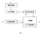
- FIG. 1 is a schematic diagram showing the structure of a camera storage system based on a physical unclonable function according to the present invention.
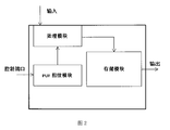
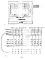
- Fig. 2 is a block diagram showing the structure of a memory portion in the present invention.
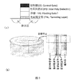
- FIG. 3 is a schematic diagram of two different configurations of non-volatile NAND flash memory cells.
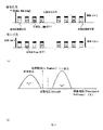
- FIG. 4 is a schematic diagram of non-uniform characteristics of information stored in a NAND memory cell array of a planar floating gate structure.
- Figure 5 is a schematic diagram of generating a memory fingerprint.
- Figure 6 is a schematic illustration of a fingerprint extraction space in a memory.
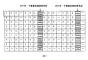
- Figure 7 is a schematic illustration of the present invention in an image storage application.
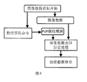
- Figure 8 is an embodiment of the application and image storage of the present invention.
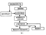
- Figure 9 is another embodiment of the application and portrait storage of the present invention.
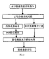
- Figure 10 is an embodiment of the present invention applied to the reading of encrypted portraits.
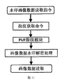
- Figure 11 is another embodiment of the present invention applied to the reading of encrypted portraits.
- the invention is based on a physical unclonable function camera storage system, as shown in FIG. 1 , including image transmissions connected in sequence Sensor, A/D converter, digital signal processor, memory and wireless communication module.
- the memory includes a processing module, a PUF fingerprint module, and a storage module.
- the processing module can select the number of bits of pixel information for performing the logical operation, and can also receive the value generated by the PUF fingerprint module for logical operation.
- the use of the PUF fingerprint module is not static, it can be selected by artificial settings, and the value generated by a certain part of the PUF fingerprint module is selected.
- the optical signal enters the camera, passes through the optical processing of the image sensor, enters the A/D converter, turns the analog signal into a digital signal, and then passes through the digital signal processor.
- the process saves the image pixel information to the memory.
- the storage portion of the image pixel information of the present invention is different from the prior art in that, when the information is saved, the lowest bit of the pixel information to be stored is associated with the PUF fingerprint module to achieve the purpose of embedding the watermark.
- the processing module of the memory selects any number of bits of the stored pixel information, but must include the lowest bit of the pixel information, and logically operates the selected bit with the value of the PUF fingerprint module selected by the user to control the PUF fingerprint module.
- the lowest value of the calculated value instead of the pixel information is stored in the memory module of the memory together with the other bits of the pixel information.
- the method for extracting chip fingerprints in the PUF fingerprint module is various.
- the user can select the extracted sector; for a specific sector, The PUF fingerprint module designated as the chip fingerprint exclusive area by the word line is extracted according to the selection of the word line. When extracting, the user can select the order of the word lines.
- each bit of the pixel information is XORed with the value generated by the selected PUF module, and the result of the XOR is returned to The lowest bit of the pixel information, so that the watermark is embedded in the image information. If each bit of the pixel information is XORed with the value generated by the selected PUF fingerprint module, the process is somewhat cumbersome, so the pixel information can be selected. The bit is XORed with the PUF fingerprint module. Note that the selected bits must include the lowest bit of the pixel information, so as to ensure that the original information of the image is restored when the image is decrypted.
- the present invention provides one more wireless communication device than the conventional camera storage system, which uses M2M technology to establish communication with the PC.
- the image information to be saved can be transmitted to the established PC end and saved by the M2M technology through the wireless communication module of the system.
- the image After the camera takes a picture, the image automatically adds the information of the watermark through hardware.
- the watermark information is added by hardware. According to the uniqueness of the PUF, the process of adding the watermark information cannot be speculated or copied. Also, if you want to get the original image, you must base it on the original memory and system environment.
- the PUF fingerprint module can be selected through a control port, that is, the watermark information added by storing the picture can be realized by selecting the PUF fingerprint information, and the user can select which part of the PUF fingerprint information to use by setting. Make the embedded watermark information more concealed. The user can also choose to use the fixed part of the PUF fingerprint information, so that the captured image has the same watermark information and becomes the exclusive mark of the photographer.
- the present invention utilizes the non-uniformity and distribution characteristics of the physical information stored by the memory, such as the number of electrons written in the floating gate of the two-dimensional NAND flash memory, the number of electrons trapped in the charge trapping layer of the three-dimensional NAND flash memory, and the ReRAM memrist memory.
- the thickness of the conductive filaments, etc. is obtained by system parameter design to obtain the PUF (Physical Unclonable Function) fingerprint information of the memory and the non-reproducible PUF (Physical Unclonable Function) fingerprint information, and the data information to be stored is associated with the PUF fingerprint information, for example, logical operation, associated Data is saved as encrypted data to local storage or transmitted via network data Save and save to the cloud storage system.
- Figure 3 shows two different configurations of non-volatile NAND flash memory cells.
- (a) is a planar floating gate structure NAND memory cell comprising: a control gate, a charge blocking layer, a floating gate layer, a charge tunneling layer, a substrate channel layer, and a source-drain doping region;
- (b) is a three-dimensional
- the NAND memory cell of the stereoscopic vertical ring channel structure comprises: a control gate, a charge blocking layer, a charge trapping layer, a charge buffer layer and a polysilicon ring channel layer.
- the NAND memory cell of the planar floating gate structure realizes the information storage function by storing electrons in the floating gate layer, and the NAND memory cell of the three-dimensional vertical annular channel structure captures electrons through defects existing in the charge trapping layer. Information storage function.
- Figure 4 shows the non-uniformity of the information stored in the NAND memory cell array of the planar floating gate structure.
- the fingerprint generation of the memory is shown in Figure 5.
- the memory cell array is put into the write state according to a special charge writing mode, and the specific values of VL (distributed left end) and VR (distributed right end) are derived, and VPUF (fingerprint read voltage) is determined by a simple algorithm.
- VPUF (VL+VR)/2 when completely uniformly distributed.
- VPUF values need to be fine-tuned left and right during non-uniform distribution to satisfy the same number of memory cells between VL and VPUF and the number of memory cells between VPUF and VR. , thereby distinguishing between the low threshold region "1" and the high threshold region "0".
- the bit information of the memory cell array can be read out by reading the voltage through the VPUF fingerprint. Even if the device process and the system design are identical between the chip and the chip, the number of stored electrons corresponding to each memory cell is completely uncontrollable and cannot be copied, so it has very high security.
- Figure 6 shows the chip fingerprint extraction space (the way in which the chip fingerprint area is selected) in the chip structure of the memory.
- Fingerprint information acquired by the fingerprint-specific area (bit information of "0" and "1") can be derived as a chip fingerprint for data encryption.
- Figure 7 shows the application of the present invention to image storage.
- the information in the box (1 Byte) represents a pixel information, and so on, each pixel information has a lowest bit, called the least significant bit.
- the pixel information of a certain number of bits can be selected to perform a logical operation operation with the value generated by the selected PUF fingerprint module, and the obtained value is brought to the lowest position of the pixel information. Due to the unintelligibility of the chip fingerprint, the lowest bit of the pixel information is finally It is also unknown that gray is used instead.
- Figure 8 shows an embodiment of the invention applied to image storage.
- the fingerprint acquisition command is excited on the one hand, and then the chip fingerprint information is read into the PUF fingerprint module according to the instruction; on the other hand, the image original data is acquired in the cache.
- the image data is associated with the chip fingerprint by a logical operation or the like, that is, the image data is subjected to watermark encryption processing, and the encrypted data is stored in the local storage system. This will allow you to see the image even if you can Unable to decrypt the chip fingerprint to ensure that the exclusive rights of the image are not violated.
- Fig. 9 shows another embodiment of the present invention applied to image storage.
- the fingerprint acquisition command is excited on the one hand, and then the chip fingerprint information is read into the PUF fingerprint module according to the instruction; on the other hand, the image original data is acquired in the cache.
- the image data is associated with the chip fingerprint through a logical operation or the like, that is, the image data is subjected to watermark encryption processing, and the processed data is connected to the cloud storage system, and the data is sent to the cloud storage system instead of being stored locally.
- the system saves.
- FIG 10 shows an embodiment of the invention applied to the reading of encrypted portraits.
- the cloud storage system is connected, the fingerprint reading command is obtained to read the chip fingerprint information of the PUF fingerprint module, and the encrypted data is simultaneously downloaded; thereafter, the image data is watermarked by the associated instruction designed by the chip system.
- the decryption process is performed, and finally the image raw data can be obtained.
- the image decryption must be performed in the memory chip system for image data acquisition. That is, the storage system where the image information is decrypted must be completely consistent with the storage system in which the image information is encrypted to implement the watermark decryption.
- Figure 11 shows another embodiment of the present invention applied to the reading of encrypted portraits.
- an image data reading instruction is issued to the local storage system
- a fingerprint reading command is obtained to read the chip fingerprint information of the PUF fingerprint module
- the image data watermark is decrypted by an associated instruction designed by the chip system, and finally the image is obtained.
- Raw data the storage system in which the image information is encrypted must be exactly the same as the storage system in which the image information is decrypted in order to implement the watermark decryption, so that copying the watermark encrypted data to another storage system cannot perform the decryption operation.
Landscapes
- Engineering & Computer Science (AREA)
- Computer Security & Cryptography (AREA)
- Computer Networks & Wireless Communication (AREA)
- Signal Processing (AREA)
- Physics & Mathematics (AREA)
- General Physics & Mathematics (AREA)
- Theoretical Computer Science (AREA)
- Storage Device Security (AREA)
- Studio Devices (AREA)
- Collating Specific Patterns (AREA)
- Image Processing (AREA)
Abstract
一种基于PUF的照相机图像存储系统;包括依次连接的图像传感器、A/D转换器、数字信号处理器和存储器,存储器包括处理模块、PUF指纹模块和存储模块,光信号进入相机,经过图像传感器光学处理后进入A/D转换器,将模拟信号变为数字信号,再经过数字信号处理器的处理将图像像素信息保存到存储器,处理模块接收到数字信号处理器处理后的信息进行处理,选择进行逻辑运算操作的像素信息位数以及接收PUF指纹模块生成的值进行逻辑运算。该系统完全基于不可复制的存储芯片的物理信息,加密后的数据具有不可复制性和不可破解性,从而可以达到高可靠性数据加密的目的,使得嵌入的水印信息更具有隐蔽性,实现存储到PC端的及时性与方便性。
Description
本发明涉及一种基于物理不可克隆函数(PUF)的照相机图像数据存储系统,属于数据加密存储技术领域。
物理不可克隆函数(Physical Unclonable Function,PUF)是指对一个物理实体输入一个激励,利用其不可避免的内在物理构造的随机差异输出一个不可预测的响应。PUF的最基本应用就是利用实体的唯一标识来实现认证。如中国专利文献CN103888268A公开的一种基于PUF身份验证和信息加密的手机耳机,是在耳机音频接口和耳机扬声器之间设有PUF指纹模块并嵌装在手机耳机内,PUF指纹模块包括能量采集器、双工通讯器、静态存储器、纠错解码器和加密电路,能量采集器、双工通讯器与耳机音频接口相连接,该能量采集器通过音频接口获取电压及电流并进行处理后为其他模块供电,双工通讯器通过耳机音频接口与手机进行双向通讯,该双工通讯器还与静态存储器、加密电路相连接,静态存储器与纠错解码器相连接,纠错解码器与加密电路相连接,该加密电路还与耳机扬声器相连接。采用PUF技术,通过硬件加密突破了现有加密算法存在的安全性问题。
在云存储和大数据高速发展的今天,信息存储安全性显得尤为重要。无法复制的存储芯片指纹、逻辑电路芯片指纹以及大数据系统指纹的研究开发是非常必要的。
图像水印的方法一直是图像处理中的一个重要的课题。目前存在的图像水印方法有通过软件将水印信息嵌入到图像中,还有通过逻辑电路实现水印的嵌入,这些方法都是通过设置密钥,经过一系列算法获得水印信息的,有的算法过程非常复杂,但结果是有规律可循的。一旦密钥和算法泄露,图像的安全性就不能得到保障。
发明内容
本发明针对现有图像处理技术存在的不足,提供一种高可靠性数据加密、更具有隐蔽性的基于PUF的照相机图像存储系统,该系统利用存储器中存储单元阵列存储信息过程的非均一性和无法复制特性,可以使图像存储于存储系统形成一对一的唯一关联性,有效防止图像的侵权使用。
本发明的基于PUF的照相机图像存储系统,采用以下技术方案:
该系统,包括依次连接的图像传感器、A/D转换器、数字信号处理器和存储器,存储器包括处理模块、PUF指纹模块和存储模块,光信号进入相机,经过图像传感器光学处理后进入A/D转换器,将模拟信号变为数字信号,再经过数字信号处理器的处理将图像像素信息保存到存储器,处理模块接收到数字信号处理器处理后的信息进行处理,进行逻辑运算操作的像素信息位数以及接收PUF指纹模块生成的值进行逻辑运算。
所述存储器在保存信息时,存储器的处理模块选择所存入像素信息的任意位数,但必须
包含像素信息的最低位,并将选择出来的位与通过使用者控制PUF指纹模块选择出来的PUF指纹模块的值进行逻辑运算,将运算所得的值替代像素信息的最低位,同像素信息的其他位一起保存到存储器的存储模块。所述将所要存储的像素信息的最低位与PUF指纹模块建立关联,是将像素信息的每一位与所选择的PUF指纹模块生成的值进行异或,异或后的结果返回到像素信息的最低位,这样就在图像信息中嵌入了水印。
所述PUF指纹模块中芯片指纹的提取方式为:对于以扇区(Block)作为芯片指纹专属区域的PUF指纹模块,按照扇区提取,提取时使用者自行选择提取的扇区;对于在特定扇区内,以字线(Word Line)指定为芯片指纹专属区域的PUF指纹模块,按照字线的选取提取,提取时使用者自行选择字线的顺序。
所述存储器与无线通信模块连接,以实现存储到PC端的及时性与方便性。
所述存储器的指纹生成过程,首先在擦除状态下使存储单元阵列进入写入状态,同时导出分布左端VL和分布右端VR的具体数值,确定指纹读取电压VPUF,在完全均一分布的时候VPUF=(VL+VR)/2,在非均一分布的时候VPUF数值需要左右微调以满足VL与VPUF之间的存储单元数目与VPUF与VR之间的存储单元数目相同,从而区分低阈值区“1”和高阈值区“0”;通过指纹读取电压VPUF将存储单元阵列的比特信息读出。
所述存储器的芯片指纹区域的选取是:对于单一存储芯片,以扇区作为芯片指纹专属区域;对于一个特定扇区,以字线指定为芯片指纹专属区域,指纹专属区域获取的指纹信息导出以作为数据加密用的芯片指纹。
本发明完全基于不可复制的存储芯片的物理信息,加密后的数据具有不可复制性和不可破解性,从而可以达到高可靠性数据加密的目的,使得嵌入的水印信息更具有隐蔽性,实现存储到PC端的及时性与方便性,可以使图像存储于存储系统形成一对一的唯一关联性,有效防止图像的侵权使用。
图1是本发明基于物理不可克隆函数的照相机存储系统的结构原理示意图。
图2是本发明中存储器部分的结构框图。
图3是两种不同构造的非挥发NAND闪存存储单元示意图。
图4是平面浮栅结构的NAND存储单元阵列存储信息非均一特性的示意图。
图5是生成存储器指纹的示意图。
图6是存储器中指纹提取空间的示意图。
图7是本发明在画像存储应用的一个示意图。
图8是本发明应用与画像存储的一个实施例。
图9是本发明应用与画像存储的另一个实施例。
图10是本发明应用于加密画像读取的一个实施例。
图11是本发明应用于加密画像读取的另一个实施例。
本发明基于物理不可克隆函数的照相机存储系统,如图1所示,包括依次连接的图像传
感器、A/D转换器、数字信号处理器、存储器和无线通信模块。如图2所示,存储器包括处理模块、PUF指纹模块和存储模块,处理模块可选择进行逻辑运算操作的像素信息位数,也能够接收PUF指纹模块生成的值进行逻辑运算。PUF指纹模块的利用不是一成不变的,它可通过人为设定进行选择,选择出PUF指纹模块某一部分生成的值。
与传统照相机存储系统的设计相同的是,在照相机使用的过程中,光信号进入相机,经过图像传感器光学处理后进入A/D转换器,将模拟信号变为数字信号,再经过数字信号处理器的处理将图像像素信息保存到存储器。
本发明在存储图像像素信息的存储部分与现有技术的不同之处是,在保存信息时,其中将所要存储的像素信息的最低位与PUF指纹模块建立关联,以达到嵌入水印的目的。存储器的处理模块选择所存入像素信息的任意位数,但必须包含像素信息的最低位,并将选择出来的位与通过使用者控制PUF指纹模块选择出来的PUF指纹模块的值进行逻辑运算,将运算所得的值替代像素信息的最低位同像素信息的其他位一起存入存储器的存储模块。其中PUF指纹模块中芯片指纹提取的方式多样,对于以扇区作为芯片指纹专属区域的PUF指纹模块,按照扇区提取,提取时,使用者可选择提取的扇区;对于在特定扇区内,以字线指定为芯片指纹专属区域的PUF指纹模块,按照字线的选取提取,提取时,使用者可自行选择字线的顺序。
所要存储的像素信息的最低位与PUF指纹模块建立关联的逻辑运算方法有很多,比如,将像素信息的每一位与所选择的PUF模块生成的值进行异或,异或后的结果返回到像素信息的最低位,这样就在图像信息中嵌入了水印,若将像素信息的每一位与所选择的PUF指纹模块生成的值进行异或,过程有些繁琐,所以可选择将像素信息的几位与PUF指纹模块进行异或,注意的是,所选择的几位必须包括像素信息的最低位,这样才能保证图像解密时将图像的原始信息还原出来。
另外,本发明比传统的照相机存储系统多了一个无线通信的装置,该装置采用M2M技术与PC端建立通信。在网络状态良好的情况下,存入像素信息的同时,可通过系统的无线通信模块,利用M2M技术将所要保存的图像信息发送到已建立连接的PC端并保存下来。
经过照相机拍照后,图像通过硬件自动加入了水印的信息,这种水印信息是硬件加入的,根据PUF的唯一性,水印信息的加入过程是不可能被推测或者复制出来。并且,若想获得原始的图像,必须基于原始存储器和系统环境。另外,利用PUF指纹模块可通过一个控制端口来选择,就是说每次存储图片加入的水印信息可通过选择PUF指纹信息来实现,使用者可通过自己设定来选择利用哪部分PUF指纹信息,这使得嵌入的水印信息更具有隐蔽性。使用者也可选择使用固定部分的PUF指纹信息,让拍摄出来的图像具有相同的水印信息,成为拍摄者的专属标记。
本发明利用存储器所存储的物理信息的非均一性和分布特性,例如二维NAND闪存存储器浮栅里写入的电子数目、三维NAND闪存存储器电荷俘获层中俘获的电子数目以及ReRAM忆阻存储器中导电细丝的粗细等,通过系统参数设计来获取上述存储器特殊的且不可复制的PUF(Physical Unclonable Function)指纹信息,将所要存储的数据信息与PUF指纹信息建立关联,例如逻辑运算,关联后的数据作为加密数据保存到本地存储器或者通过网络数据传
输保存到云存储系统。
图3给出了两种不同构造的非挥发NAND闪存存储单元。其中,(a)是平面浮栅结构的NAND存储单元,包括:控制栅、电荷阻挡层、浮栅层、电荷隧穿层、衬底沟道层和源漏掺杂区域;(b)是三维立体垂直环形沟道结构的NAND存储单元,包括:控制栅、电荷阻挡层、电荷俘获层、电荷隋婵层和多晶硅环形沟道层。平面浮栅结构的NAND存储单元实通过在浮栅层中存储电子来实现信息存储功能的,而三维立体垂直环形沟道结构的NAND存储单元则是通过电荷俘获层中存在的缺陷来俘获电子实现信息存储功能的。
图4给出了平面浮栅结构的NAND存储单元阵列存储信息非均一特性。(a)在擦除状态下,浮栅层中存在的是空穴,由于每个器件物理结构(包括材料组分、薄膜厚度和杂质分布等)上不可能完全相同,即使在同一环境和同一系统参数设计下,存储单元阵列里每个存储单元里存储的空穴数目也是多少不一;同样,通过外加栅压注入电子进行数据写入后,在写入状态下,存储单元阵列里每个存储单元里存储的电子数目也是多少不一的。(b)上述存储信息的非均一性表现在阈值电压(Threshold Voltage)分布上,在可以理解在擦除状态下和写入状态下存储信息虽然可以通过数据读取电压(Vread)简单区分为“0”和“1”,但存储单元阵列的所有存储单元的阈值电压实际上是一个比较宽的分布。
存储器的指纹生成如图5所示。首先在擦除状态下按特殊的电荷写入方式使存储单元阵列进入写入状态,同时导出VL(分布左端)和VR(分布右端)的具体数值,通过简单算法确定VPUF(指纹读取电压),在完全均一分布的时候VPUF=(VL+VR)/2,在非均一分布的时候VPUF数值需要左右微调以满足VL与VPUF之间的存储单元数目与VPUF与VR之间的存储单元数目相同,从而区分低阈值区“1”和高阈值区“0”。通过VPUF指纹读取电压则可以将存储单元阵列的比特信息读出。芯片和芯片之间即使从器件工艺到系统设计完全相同,对应到每一个存储单元存储电子数目的多少是完全不可控的,也是不可复制的,因此具有非常高的安全性。
图6给出了存储器的芯片结构中芯片指纹提取空间(芯片指纹区域的选取方式)。(a)对于单一的一个存储芯片,其中有很多扇区(Block),可以选择其中一个或几个扇区作为芯片指纹专属区域;(b)对于某个特定扇区,其中部分字线(Word Line)也可以指定为芯片指纹专属区域。指纹专属区域获取的指纹信息(“0”和“1”的比特信息)则可以导出以作为数据加密用的芯片指纹。
图7给出了本发明在画像存储的应用。其中框内(1个Byte)的信息代表一个像素信息,以此类推,每一个像素信息都有一个最低位,称为最低有效位。可以选择出某几位的像素信息与选择出的PUF指纹模块生成的值进行逻辑运算操作,将所得的值带入到像素信息最低位,由于芯片指纹的不可获知性,像素信息的最低位最后也不可得知,这里用灰色来替代。
图8给出了本发明应用于画像存储的一个实施例。在图像数据获取开始的同时,一方面激发指纹获取命令,然后根据指令到PUF指纹模块中读取芯片指纹信息;另一方面在缓存中获取图像原始数据。然后,通过逻辑运算等关联方式把图像数据和芯片指纹关联,即对画像数据进行水印加密处理,把加密后的数据保存在本地存储系统。这样可以即使能看到图像也
无法解密其芯片指纹,即可保证图片专属权的不被侵犯。
图9给出了本发明应用于画像存储的另一个实施例。在图像数据获取开始的同时,一方面激发指纹获取命令,然后根据指令到PUF指纹模块中读取芯片指纹信息;另一方面在缓存中获取图像原始数据。然后,通过逻辑运算等关联方式把图像数据和芯片指纹关联,即对画像数据进行水印加密处理,处理后的数据则是通过与云端存储系统连接,把数据发送到云端存储系统而不再本地存储系统保存。
图10给出了本发明应用于加密画像读取的一个实施例。在发出图像数据读取指令时,与云端存储系统连接,获得指纹读取命令以读取PUF指纹模块的芯片指纹信息,同时下载加密数据;其后,通过芯片系统设计的关联指令对图像数据水印进行解密处理,最后可获得图像原始数据。图像解密必须在图像数据获取的存储芯片系统里才能进行,即图像信息解密时所在的存储系统必须和图像信息加密时所在的存储系统必须完全一致才能实施水印解密。
图11给出了本发明应用于加密画像读取的另一个实施例。在对本地存储系统发出图像数据读取指令时,获得指纹读取命令以读取PUF指纹模块的芯片指纹信息,其后通过芯片系统设计的关联指令对图像数据水印进行解密处理,最后可获得图像原始数据。与前述一样,图像信息加密时所在的存储系统必须和图像信息解密时所在的存储系统必须完全一致才能实施水印解密,这样把水印加密数据复制到另外的存储系统中是无法实施解密操作的。
Claims (7)
- 一种基于PUF的照相机图像存储系统,包括依次连接的图像传感器、A/D转换器、数字信号处理器和存储器,其特征是:存储器包括处理模块、PUF指纹模块和存储模块,光信号进入相机,经过图像传感器光学处理后进入A/D转换器,将模拟信号变为数字信号,再经过数字信号处理器的处理将图像像素信息保存到存储器,处理模块接收到数字信号处理器处理后的信息进行处理,选择进行逻辑运算操作的像素信息位数以及接收PUF指纹模块生成的值进行逻辑运算。
- 根据权利要求1所述的基于PUF的照相机图像存储系统,其特征是:所述存储器在保存信息时,存储器的处理模块选择所存入像素信息的任意位数,但必须包含像素信息的最低位,并将选择出来的位与通过使用者控制PUF指纹模块选择出来的PUF指纹模块的值进行逻辑运算,将运算所得的值替代像素信息的最低位,同像素信息的其他位一起保存到存储器的存储模块。
- 根据权利要求2所述的基于PUF的照相机图像存储系统,其特征是:所述逻辑运算,是将选择出来的像素信息位与所选择的PUF指纹模块生成的值进行异或,异或后的结果返回到像素信息的最低位,这样就在图像信息中嵌入了水印。
- 根据权利要求1所述的基于PUF的照相机图像存储系统,其特征是:所述PUF指纹模块中芯片指纹的提取方式为:对于以扇区作为芯片指纹专属区域的PUF指纹模块,按照扇区提取,提取时使用者自行选择提取的扇区;对于在特定扇区内,以字线指定为芯片指纹专属区域的PUF指纹模块,按照字线的选取提取,提取时使用者自行选择字线的顺序。
- 根据权利要求1所述的基于PUF的照相机图像存储系统,其特征是:所述存储器与无线通信模块连接。
- 根据权利要求1所述的基于PUF的照相机图像存储系统,其特征是:所述存储器的指纹生成过程,首先在擦除状态下使存储单元阵列进入写入状态,同时导出分布左端VL和分布右端VR的具体数值,确定指纹读取电压VPUF,在完全均一分布的时候VPUF=(VL+VR)/2,在非均一分布的时候VPUF数值需要左右微调以满足VL与VPUF之间的存储单元数目与VPUF与VR之间的存储单元数目相同,从而区分低阈值区“1”和高阈值区“0”;通过指纹读取电压VPUF将存储单元阵列的比特信息读出。
- 根据权利要求1所述的基于PUF的照相机图像存储系统,其特征是:所述存储器的芯片指纹区域的选取是:对于单一存储芯片,以扇区作为芯片指纹专属区域;对于一个特定扇区,以字线指定为芯片指纹专属区域,指纹专属区域获取的指纹信息导出以作为数据加密用的芯片指纹。
Applications Claiming Priority (2)
| Application Number | Priority Date | Filing Date | Title |
|---|---|---|---|
| CN201710292680.2A CN106972934A (zh) | 2017-04-28 | 2017-04-28 | 一种基于puf的照相机图像存储系统 |
| CN201710292680.2 | 2017-04-28 |
Publications (1)
| Publication Number | Publication Date |
|---|---|
| WO2018196266A1 true WO2018196266A1 (zh) | 2018-11-01 |
Family
ID=59330307
Family Applications (1)
| Application Number | Title | Priority Date | Filing Date |
|---|---|---|---|
| PCT/CN2017/102556 Ceased WO2018196266A1 (zh) | 2017-04-28 | 2017-09-21 | 一种基于puf的照相机图像存储系统 |
Country Status (2)
| Country | Link |
|---|---|
| CN (1) | CN106972934A (zh) |
| WO (1) | WO2018196266A1 (zh) |
Cited By (2)
| Publication number | Priority date | Publication date | Assignee | Title |
|---|---|---|---|---|
| US20240396724A1 (en) * | 2023-05-23 | 2024-11-28 | Carnegie Mellon University | Method for key generation using physically unclonable functions |
| EP4586545A1 (en) * | 2024-01-15 | 2025-07-16 | ICTK Co., Ltd. | Device and method for generating watermarked media |
Families Citing this family (5)
| Publication number | Priority date | Publication date | Assignee | Title |
|---|---|---|---|---|
| CN106972934A (zh) * | 2017-04-28 | 2017-07-21 | 山东大学 | 一种基于puf的照相机图像存储系统 |
| EP3920165B1 (en) | 2019-01-30 | 2024-09-11 | Sony Group Corporation | Sensor device and encryption method |
| CN111783919A (zh) * | 2019-04-04 | 2020-10-16 | 利盟国际有限公司 | 在银行卡或身份证中的用于安全性的物理不可克隆功能 |
| IT201900007290A1 (it) * | 2019-05-27 | 2020-11-27 | Torino Politecnico | Apparato d'utente e metodo di protezione di dati riservati |
| CN110598488B (zh) * | 2019-09-17 | 2022-12-27 | 山东大学 | 半导体单元器件、半导体芯片系统及puf信息处理系统 |
Citations (7)
| Publication number | Priority date | Publication date | Assignee | Title |
|---|---|---|---|---|
| CN102656588A (zh) * | 2009-08-14 | 2012-09-05 | 本质Id有限责任公司 | 具有防篡改和抗老化系统的物理不可克隆函数 |
| EP2626816A1 (en) * | 2012-02-08 | 2013-08-14 | Gemalto SA | Method of authenticating a device |
| CN104810062A (zh) * | 2015-05-12 | 2015-07-29 | 东南大学 | 一种sram芯片的puf特性测试方法及装置 |
| CN205987083U (zh) * | 2016-07-28 | 2017-02-22 | 河源市新天彩科技有限公司 | 一种照相机系统 |
| CN106503721A (zh) * | 2016-10-27 | 2017-03-15 | 河海大学常州校区 | 基于cmos图像传感器puf的哈希算法及认证方法 |
| US20170103791A1 (en) * | 2015-10-09 | 2017-04-13 | Lexmark International, Inc. | Rotating Magnetic Measurements of Physical Unclonable Functions |
| CN106972934A (zh) * | 2017-04-28 | 2017-07-21 | 山东大学 | 一种基于puf的照相机图像存储系统 |
Family Cites Families (3)
| Publication number | Priority date | Publication date | Assignee | Title |
|---|---|---|---|---|
| DE102010041447A1 (de) * | 2010-09-27 | 2012-03-29 | Robert Bosch Gmbh | Verfahren zum Authentifizieren eines ladungsgekoppelten Bauteils (CCD) |
| CN104794673B (zh) * | 2015-03-30 | 2017-12-08 | 北京交通大学 | 利用最高有效位的加密域可逆数字水印实现方法 |
| CN105978889B (zh) * | 2016-06-20 | 2019-06-11 | 北京集创北方科技股份有限公司 | 生物特征加密方法及装置 |
-
2017
- 2017-04-28 CN CN201710292680.2A patent/CN106972934A/zh active Pending
- 2017-09-21 WO PCT/CN2017/102556 patent/WO2018196266A1/zh not_active Ceased
Patent Citations (7)
| Publication number | Priority date | Publication date | Assignee | Title |
|---|---|---|---|---|
| CN102656588A (zh) * | 2009-08-14 | 2012-09-05 | 本质Id有限责任公司 | 具有防篡改和抗老化系统的物理不可克隆函数 |
| EP2626816A1 (en) * | 2012-02-08 | 2013-08-14 | Gemalto SA | Method of authenticating a device |
| CN104810062A (zh) * | 2015-05-12 | 2015-07-29 | 东南大学 | 一种sram芯片的puf特性测试方法及装置 |
| US20170103791A1 (en) * | 2015-10-09 | 2017-04-13 | Lexmark International, Inc. | Rotating Magnetic Measurements of Physical Unclonable Functions |
| CN205987083U (zh) * | 2016-07-28 | 2017-02-22 | 河源市新天彩科技有限公司 | 一种照相机系统 |
| CN106503721A (zh) * | 2016-10-27 | 2017-03-15 | 河海大学常州校区 | 基于cmos图像传感器puf的哈希算法及认证方法 |
| CN106972934A (zh) * | 2017-04-28 | 2017-07-21 | 山东大学 | 一种基于puf的照相机图像存储系统 |
Cited By (2)
| Publication number | Priority date | Publication date | Assignee | Title |
|---|---|---|---|---|
| US20240396724A1 (en) * | 2023-05-23 | 2024-11-28 | Carnegie Mellon University | Method for key generation using physically unclonable functions |
| EP4586545A1 (en) * | 2024-01-15 | 2025-07-16 | ICTK Co., Ltd. | Device and method for generating watermarked media |
Also Published As
| Publication number | Publication date |
|---|---|
| CN106972934A (zh) | 2017-07-21 |
Similar Documents
| Publication | Publication Date | Title |
|---|---|---|
| WO2018196266A1 (zh) | 一种基于puf的照相机图像存储系统 | |
| US10097348B2 (en) | Device bound encrypted data | |
| JP5662037B2 (ja) | 不揮発性メモリに対してデータの読み出しおよび書き込みを行うためのデータホワイトニング | |
| CN103427979B (zh) | 一种基于混沌加密的互联网图片透明安全传输方法 | |
| US10044703B2 (en) | User device performing password based authentication and password registration and authentication methods thereof | |
| CN110753226B (zh) | 一种高容量密文域图像可逆数据隐藏方法 | |
| CN104851070B (zh) | 一种基于前景和背景分离的图像加密和解密方法 | |
| CN104881374A (zh) | 自加密驱动器和包括自加密驱动器的用户装置 | |
| US10809925B2 (en) | Configurable security memory region | |
| JP2013243667A (ja) | 記憶装置の識別子を基盤とするコンテンツの暗復号化装置及び方法 | |
| CN104145274A (zh) | 基于生物测定数据的媒体加密 | |
| WO2017215148A1 (zh) | 文件保护方法及装置 | |
| US11706382B2 (en) | Methods and apparatus for encrypting camera media | |
| US20170104593A1 (en) | Key storage methods | |
| US20220309194A1 (en) | Key based partial data restriction in storage systems | |
| CN115017556A (zh) | 具有加密功能的存储设备 | |
| WO2019184741A1 (zh) | 应用程序信息的存储、处理方法及装置 | |
| CN111131130A (zh) | 密钥管理方法及系统 | |
| US11824977B2 (en) | Data processing system and method | |
| US20200272748A1 (en) | Methods and apparatus for validating media content | |
| CN109829322B (zh) | 基于授权信息的数媒文件实时加解密方法与系统 | |
| CN103873227A (zh) | 一种fpga加密数据流的解密电路及解密方法 | |
| CN114465779A (zh) | 一种可逆可分离的密文域信息隐藏方法及系统 | |
| CN118158343A (zh) | 视频数据加解密方法、计算设备以及计算机可读存储介质 | |
| US11321323B2 (en) | Method and system for searching for at least a specific datum in a user unit |
Legal Events
| Date | Code | Title | Description |
|---|---|---|---|
| 121 | Ep: the epo has been informed by wipo that ep was designated in this application |
Ref document number: 17907906 Country of ref document: EP Kind code of ref document: A1 |
|
| NENP | Non-entry into the national phase |
Ref country code: DE |
|
| 122 | Ep: pct application non-entry in european phase |
Ref document number: 17907906 Country of ref document: EP Kind code of ref document: A1 |