WO2018179115A1 - 荷電粒子線装置 - Google Patents
荷電粒子線装置 Download PDFInfo
- Publication number
- WO2018179115A1 WO2018179115A1 PCT/JP2017/012782 JP2017012782W WO2018179115A1 WO 2018179115 A1 WO2018179115 A1 WO 2018179115A1 JP 2017012782 W JP2017012782 W JP 2017012782W WO 2018179115 A1 WO2018179115 A1 WO 2018179115A1
- Authority
- WO
- WIPO (PCT)
- Prior art keywords
- charged particle
- sample
- pole piece
- particle beam
- magnetic pole
- Prior art date
- Legal status (The legal status is an assumption and is not a legal conclusion. Google has not performed a legal analysis and makes no representation as to the accuracy of the status listed.)
- Ceased
Links
Images



Classifications
-
- H—ELECTRICITY
- H01—ELECTRIC ELEMENTS
- H01J—ELECTRIC DISCHARGE TUBES OR DISCHARGE LAMPS
- H01J37/00—Discharge tubes with provision for introducing objects or material to be exposed to the discharge, e.g. for the purpose of examination or processing thereof
- H01J37/02—Details
- H01J37/04—Arrangements of electrodes and associated parts for generating or controlling the discharge, e.g. electron-optical arrangement or ion-optical arrangement
-
- H—ELECTRICITY
- H01—ELECTRIC ELEMENTS
- H01J—ELECTRIC DISCHARGE TUBES OR DISCHARGE LAMPS
- H01J37/00—Discharge tubes with provision for introducing objects or material to be exposed to the discharge, e.g. for the purpose of examination or processing thereof
- H01J37/26—Electron or ion microscopes; Electron or ion diffraction tubes
- H01J37/28—Electron or ion microscopes; Electron or ion diffraction tubes with scanning beams
-
- H—ELECTRICITY
- H01—ELECTRIC ELEMENTS
- H01J—ELECTRIC DISCHARGE TUBES OR DISCHARGE LAMPS
- H01J37/00—Discharge tubes with provision for introducing objects or material to be exposed to the discharge, e.g. for the purpose of examination or processing thereof
- H01J37/02—Details
- H01J37/04—Arrangements of electrodes and associated parts for generating or controlling the discharge, e.g. electron-optical arrangement or ion-optical arrangement
- H01J37/10—Lenses
- H01J37/12—Lenses electrostatic
-
- H—ELECTRICITY
- H01—ELECTRIC ELEMENTS
- H01J—ELECTRIC DISCHARGE TUBES OR DISCHARGE LAMPS
- H01J37/00—Discharge tubes with provision for introducing objects or material to be exposed to the discharge, e.g. for the purpose of examination or processing thereof
- H01J37/02—Details
- H01J37/04—Arrangements of electrodes and associated parts for generating or controlling the discharge, e.g. electron-optical arrangement or ion-optical arrangement
- H01J37/10—Lenses
- H01J37/14—Lenses magnetic
- H01J37/141—Electromagnetic lenses
-
- H—ELECTRICITY
- H01—ELECTRIC ELEMENTS
- H01J—ELECTRIC DISCHARGE TUBES OR DISCHARGE LAMPS
- H01J37/00—Discharge tubes with provision for introducing objects or material to be exposed to the discharge, e.g. for the purpose of examination or processing thereof
- H01J37/02—Details
- H01J37/04—Arrangements of electrodes and associated parts for generating or controlling the discharge, e.g. electron-optical arrangement or ion-optical arrangement
- H01J37/10—Lenses
- H01J37/145—Combinations of electrostatic and magnetic lenses
-
- H—ELECTRICITY
- H01—ELECTRIC ELEMENTS
- H01J—ELECTRIC DISCHARGE TUBES OR DISCHARGE LAMPS
- H01J37/00—Discharge tubes with provision for introducing objects or material to be exposed to the discharge, e.g. for the purpose of examination or processing thereof
- H01J37/02—Details
- H01J37/04—Arrangements of electrodes and associated parts for generating or controlling the discharge, e.g. electron-optical arrangement or ion-optical arrangement
- H01J37/153—Electron-optical or ion-optical arrangements for the correction of image defects, e.g. stigmators
-
- H—ELECTRICITY
- H01—ELECTRIC ELEMENTS
- H01J—ELECTRIC DISCHARGE TUBES OR DISCHARGE LAMPS
- H01J2237/00—Discharge tubes exposing object to beam, e.g. for analysis treatment, etching, imaging
- H01J2237/04—Means for controlling the discharge
- H01J2237/047—Changing particle velocity
- H01J2237/0473—Changing particle velocity accelerating
- H01J2237/04735—Changing particle velocity accelerating with electrostatic means
-
- H—ELECTRICITY
- H01—ELECTRIC ELEMENTS
- H01J—ELECTRIC DISCHARGE TUBES OR DISCHARGE LAMPS
- H01J2237/00—Discharge tubes exposing object to beam, e.g. for analysis treatment, etching, imaging
- H01J2237/04—Means for controlling the discharge
- H01J2237/047—Changing particle velocity
- H01J2237/0475—Changing particle velocity decelerating
- H01J2237/04756—Changing particle velocity decelerating with electrostatic means
-
- H—ELECTRICITY
- H01—ELECTRIC ELEMENTS
- H01J—ELECTRIC DISCHARGE TUBES OR DISCHARGE LAMPS
- H01J2237/00—Discharge tubes exposing object to beam, e.g. for analysis treatment, etching, imaging
- H01J2237/04—Means for controlling the discharge
- H01J2237/049—Focusing means
- H01J2237/0492—Lens systems
- H01J2237/04926—Lens systems combined
-
- H—ELECTRICITY
- H01—ELECTRIC ELEMENTS
- H01J—ELECTRIC DISCHARGE TUBES OR DISCHARGE LAMPS
- H01J2237/00—Discharge tubes exposing object to beam, e.g. for analysis treatment, etching, imaging
- H01J2237/10—Lenses
- H01J2237/14—Lenses magnetic
- H01J2237/1405—Constructional details
-
- H—ELECTRICITY
- H01—ELECTRIC ELEMENTS
- H01J—ELECTRIC DISCHARGE TUBES OR DISCHARGE LAMPS
- H01J2237/00—Discharge tubes exposing object to beam, e.g. for analysis treatment, etching, imaging
- H01J2237/10—Lenses
- H01J2237/14—Lenses magnetic
- H01J2237/1405—Constructional details
- H01J2237/141—Coils
Definitions
- the present invention relates to a charged particle beam apparatus.
- Patent Document 1 In a charged particle beam apparatus, a technique using a boosting magnetic field lens in which an electric field lens is superimposed is disclosed (see Patent Document 1).
- the advantage of the objective lens of Patent Document 1 is, for example, high resolution in low energy observation by a decelerating electrostatic field.
- Patent Document 1 there is a problem that the resolution may deteriorate depending on the condition of the sample. For example, when the surface of the sample has irregularities, or when the sample is inclined with respect to the optical axis through which the charged particle beam passes, the electric field lens formed on the sample is distorted, and the performance of the objective lens deteriorates.
- an object of the present invention is to provide a charged particle beam apparatus that can realize high-resolution observation by suppressing distortion of an electric field lens.
- a charged particle beam apparatus is disposed between a charged particle source that emits a charged particle beam and the charged particle source and the sample, and forms a passage for the charged particle beam.
- a first lens coil that is disposed outside the second magnetic pole piece and disposed inside the second magnetic pole piece to form a first lens, and is disposed outside the second magnetic pole piece to form a second lens.
- the second lens coil to be formed, and the electric field formed between the tip of the first magnetic pole piece and the tip of the second magnetic pole piece is controlled between the sample and the tip of the second magnetic pole piece.
- a control electrode is disposed between a charged particle source that emits a charged particle beam and the charged particle source and the sample, and forms a passage for the charged particle beam.
- the present invention it is possible to provide a charged particle beam apparatus capable of realizing high resolution observation by suppressing distortion of an electric field lens.
- a scanning electron microscope hereinafter referred to as SEM
- SEM scanning electron microscope
- FIB-SEM focused ion beam-scanning electron microscope combined apparatus
- STEM scanning transmission electron microscope
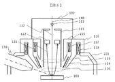
- FIG. 1 is a schematic diagram of an SEM.
- the SEM includes a SEM casing 102 that irradiates a sample 103 with a primary charged particle beam (here, a primary electron beam), a sample chamber 101 that mounts the casing 102 and accommodates a sample during observation, and a sample chamber 101.
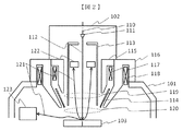
- FIG. 2 is a detailed view of the SEM.
- the SEM casing 102 includes an electron source 111 that emits a primary electron beam 112, an objective lens that focuses the primary electron beam 112 on the sample 103, and accelerates the primary electron beam 112 from directly below the electron source 110 to the tip of the objective lens.
- a boosting electrode 113 and a control electrode 114 for passing the objective lens in a high energy state, and detectors 122 and 123 for detecting signal electrons 121 generated from the sample 103 by irradiation of the primary electron beam 112 are provided.
- the primary electron beam 112 is accelerated by the boosting electrode 113 and the control electrode 114, the energy of the primary electron beam 112 when receiving the focusing action by the objective lens is increased, so that the lens aberration is reduced and the resolution is improved.
- the objective lens is an electric field superposition type magnetic lens and has two modes.
- One is a non-immersion type magnetic lens 119 (non-immersion mode) with no leakage of the magnetic field on the sample
- the other is an immersion type magnetic lens 120 (immersion mode) that forms a magnetic field on the sample.
- the former is suitable for analysis without magnetic field effects and observation of magnetic samples because there is no magnetic field leakage onto the sample, and the latter is suitable for high-resolution observations by forming a magnetic field on the sample and reducing the lens focal length. ing. In this way, a wide range of analysis is possible by properly using the lens mode of the magnetic lens according to the application.
- the non-immersion type magnetic lens 119 (first lens) is configured to flow current through a first lens coil 117 disposed outside the first magnetic pole piece 115 and inside the second magnetic pole piece 116. , Formed between the first pole piece 115 and the second pole piece 116.
- the immersion type magnetic lens 120 (second lens) causes the second magnetic pole piece 116 and the sample 103 to flow by passing a current through the second lens coil 118 disposed outside the second magnetic pole piece 116. Formed between.
- the first magnetic pole piece 115 and the second magnetic pole piece 116 have an axisymmetric hollow conical shape and are made of a soft magnetic material such as pure iron or permendur. Further, the opening on the sample side of the second magnetic pole piece 116 is smaller than the opening on the sample side of the first magnetic pole piece 115.
- the first magnetic pole piece 115 and the second magnetic pole piece 116 are arranged between the electron source 111 and the sample 103, and the second magnetic pole piece 116 is arranged outside the first magnetic pole piece 115.
- the sample-side tip of the second magnetic pole piece 116 is disposed closer to the sample than the sample-side tip of the first magnetic pole piece.
- Detectors that detect signal electrons include an in-housing detector 122 mounted in the SEM housing 102 and a sample chamber detector 123 mounted in the sample chamber 101.
- a detector using a scintillator A detector using a semiconductor is used.
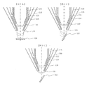
- FIG. 3 is a schematic diagram of a deceleration electric field, where A is a second deceleration electric field formed on the sample, B is a second deceleration electric field when the sample is tilted, and C is a suppressed second deceleration electric field. .
- the boosting electrode 113 has a hollow cylindrical shape that is axisymmetric with respect to the optical axis 110, is disposed inside the first magnetic pole piece 115, and directly below the electron source from the tip of the first magnetic pole piece 115 on the sample side. Arranged to the bottom.
- the control electrode 114 has a hollow conical shape that is axisymmetric with respect to the optical axis 110, and is disposed between the boosting electrode 113 and the second magnetic pole piece 116.
- a positive voltage is applied to the boosting electrode 113, and a voltage lower than that of the boosting electrode 113 and higher than that of the sample 103 is applied to the control electrode 114.
- a first deceleration electric field 130 that decelerates the primary electron beam 112 is formed by the potential difference, and the potential difference between the control electrode 114, the second magnetic pole piece 116, and the sample 103.
- a second deceleration electric field 131 that decelerates the primary electron beam 112 is formed.
- the distance between the tip of the second magnetic pole piece 116 and the sample 103 and the voltage applied to the control electrode 114 are set to appropriate values.
- the second deceleration electric field 131 is mainly formed by the potential difference between the control electrode 114 and the second magnetic pole piece 116, and electric field leakage onto the sample 103 can be suppressed.
- the boosting electrode 113, the control electrode 114, the second magnetic pole piece 116, and the sample 103 are arranged electrically independently from each other, the voltage applied to the sample 103 is Vs, and the voltage applied to the control electrode 114. Is defined as Vc, and the voltage applied to the boosting electrode 113 is defined as Vb, Vs ⁇ Vc ⁇ Vb is satisfied.
- the distance between the tip of the second magnetic pole piece 116 and the sample 103 is 4 mm
- the voltage value of the control electrode 114 is about 100 V with respect to the grounded sample
- the electric field leakage on the sample Can be suppressed.
- the voltage values of the boosting electrode 113 and the control electrode 114 can be arbitrarily changed by a GUI (display unit 104) for operating the SEM. Therefore, the voltage value of the electrode can be easily changed depending on the observation conditions.
- the voltage of the boosting electrode 113 is set to a constant value, and only the voltage value of the control electrode is changed, so that the optical condition does not change with the change of the voltage value of the boosting electrode 113.
- An objective lens can be used.
- the primary electron beam 112 emitted from the electron source 111 travels in the cylinder of the boosting electrode 113 at a high speed.
- the primary electron beam 112 is focused by the non-immersion type magnetic lens 119, and then decelerated by the first deceleration electric field 130 and the second deceleration electric field 131 and irradiated on the sample 103.
- the primary electron beam 112 is decelerated by the first decelerating electric field 130, then receives a focusing action by the immersion type magnetic lens 120, and then the second decelerating electric field formed on the sample 103.
- the sample 103 is decelerated by 131 and irradiated onto the sample 103.
- the primary electron beam 112 is subjected to the focusing action by the magnetic lens with high energy, so that aberration generated when passing through the magnetic lens can be reduced.
- the primary electron beam 112 focused by the lens action scans the sample by the deflection action of the scanning coil.
- signal electrons 121 are emitted.
- the signal electrons 121 are detected by the in-casing detector 122 or the sample chamber detector 123.
- the deceleration action of the first deceleration electric field 130 and the second deceleration electric field 131 can be controlled.
- the potential of the control electrode 114 is set to the sample potential. Control may be performed so as to be close to.
- the voltage value of the control electrode 114 is set high in order to increase the second deceleration electric field 131.
- the voltage value of the control electrode 114 is set to the second value in order to weaken the second deceleration electric field 131. It is set to be close to the potential of the pole piece and the sample.
- control electrode 114 can suppress the distortion of the deceleration electric field on the sample, which is a problem in boosting the objective lens.
- the signal electrons 121 are secondary electrons having a low energy of about 50 eV, they are sucked into the SEM casing 102 by the second deceleration electric field 131.
- backscattered electrons having relatively high energy compared to the secondary electrons are not focused by the second deceleration electric field 131 and go straight. Therefore, it is possible to discriminate secondary electrons and backscattered electrons according to the intensity of the first and second deceleration electric fields 131 and the arrangement of the detectors.
- FIG. 4 is a cross-sectional view of the division unit 141 of various components forming the objective lens.
- A shows how the division unit 141 is divided from the SEM.
- the B splitting unit 141 includes a sample-side tip of the boosting electrode, a control electrode, a sample-side tip of the first magnetic pole piece, and a sample-side tip of the second magnetic pole piece.
- C shows an example in which the sample-side tip of the first magnetic pole piece is not included in the division unit 141.
- various components can be structured to be detachable from the SEM as required. This facilitates repair when the electrodes and pole pieces for forming the objective lens are contaminated by adhesion of impurities, adsorption of gas, or the like or damaged by interferences, thereby improving maintainability.
- FIG. 5 is a cross-sectional view of the in-housing detector 22 mounted on the divided portion.
- a deflector for deflecting an electron beam and a throttle hole for differential exhaust can be mounted at the divided portion.
- the division unit 141 has an advantage that it is easy to insert other components into the division part.
- the insulating member 140 (resin material, ceramic material, etc.) It is fixed using.
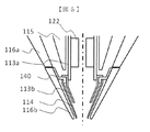
- FIGS. 6A and 6B are schematic views of the fixing method of the divided unit, in which A is a method of fixing directly on the second magnetic pole piece 116a with a screw, and B is a second magnetic pole directly on the screw cut on the second magnetic pole piece 116a.
- C and D indicate a method of fixing the lower half 116b, and C and D indicate a method of fixing using an insulator such as a resin material or a ceramic material.
- C is fixed on the second magnetic pole piece, and D is fixed on the first magnetic pole piece. In either case, it is assumed that the end face on the second magnetic pole piece and the end face under the second magnetic pole piece are joined without a gap.
- fixing by resin fitting or fixing using magnetic attraction is possible.
- the assembling accuracy of the first and second magnetic pole pieces forming the magnetic lens, the boosting electrode forming the electric field lens, and the control electrode position is important.
- these parts that require assembling accuracy are grouped as a divided unit, thereby providing an advantage that the assemblability can be improved as a result of downsizing and the divided unit can be provided as a consumable.
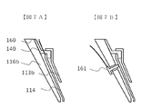
- FIG. 7 is a schematic diagram of a method for introducing a voltage to the control electrode, where A is a method of introducing from a divided portion of the second magnetic pole piece, and B is a method of introducing from a hole formed in the side surface of the second magnetic pole piece. Show. It is preferable to provide 2 to 4 holes symmetrically.
- the method for introducing the voltage to the lower boosting electrode 113b may be a method for joining the upper boosting electrode 113a at the divided portion or a method for introducing the voltage from the outside of the second magnetic pole piece in the same manner as the control electrode. As a joining method, joining using a spring, joining using a cable, and the like are possible.
- Example 1 by adding a control electrode in addition to a boosting electrode for accelerating a charged particle beam, high-resolution observation by electric field superposition can be realized regardless of the mode of the objective lens.
- a charged particle beam apparatus that achieves both high-resolution observation and electromagnetic field-free observation on a sample.
- functions can be stably provided by improving assemblability and maintenance.
- FIG. 8 is a schematic diagram of an FIB-SEM (Focused Ion Beam; also referred to as a composite charged particle beam apparatus).
- FIB-SEM Fluorous Ion Beam
- the FIB casing 170 is mounted toward the sample, and the sample is processed by the FIB.
- the sample is tilted so as to be orthogonal to the central axis of the FIB casing 170, and processing is performed by an ion beam.
- FIB-SEM SEM objective lens it is effective as a FIB-SEM SEM objective lens to use the tip of the objective lens as a split unit.
- sputtered particles atoms / molecules
- the sputtered particles adhere to the tip of the objective lens, which may cause problems such as a discharge due to a deterioration in performance of the in-housing detector and a deterioration in insulation performance between the electrodes.
- the structure in which the pole piece and the tip of the electrode on the sample side are detachable can be easily replaced when a defect in the detector in the housing or the electrode occurs.
- SYMBOLS 100 Base, 101 ... Sample chamber, 102 ... SEM housing, 103 ... Sample, 104 ... Monitor, 105 ... Control part, 110 ... Optical axis, 111 ... Electron source, 112 ... Primary electron beam, 113 ... Boosting electrode, 113a ... on boosting electrode, 113b ... under boosting electrode, 114 ... control electrode, 115 ... first magnetic pole piece, 116 ... second magnetic pole piece, 116a ... on second magnetic pole piece, 116b ...
Landscapes
- Chemical & Material Sciences (AREA)
- Analytical Chemistry (AREA)
- Physics & Mathematics (AREA)
- Electromagnetism (AREA)
- Analysing Materials By The Use Of Radiation (AREA)
Abstract
Description
Claims (12)
- 荷電粒子線を放出する荷電粒子源と、
前記荷電粒子源と前記試料との間に配置され、前記荷電粒子線の通路を形成すると共に、該記荷電粒子線を加減速するブースティング電極と、
前記ブースティング電極を覆うように形成される第一の磁極片と、
前記第一の磁極片を覆うように形成される第二の磁極片と、
前記第一の磁極片の外側に配置されると共に前記第二の磁極片の内側に配置され、第一のレンズを形成する第一のレンズコイルと、
前記第二の磁極片の外側に配置され、第二のレンズを形成する第二のレンズコイルと、
前記第一の磁極片の先端部と前記第二の磁極片の先端部との間に形成され、前記試料と前記第二の磁極片の先端部の間に形成させる電界を制御する制御電極と、を備える、
荷電粒子線装置。 - 前記第一のレンズとは非浸漬型レンズであり、前記第二のレンズとは浸漬型のレンズである、請求項1記載の荷電粒子線装置。
- 前記荷電粒子線装置に着脱可能に形成される分割ユニットを備え、
前記分割ユニットは、前記第二の磁極片の前記試料側の先端部を含む、請求項1記載の荷電粒子線装置。 - 前記分割ユニットは、更に、前記制御電極と、前記ブースティング電極の前記試料側の先端部を含む、請求項3記載の荷電粒子線装置。
- 前記分割ユニットと前記荷電粒子線装置との分割箇所から、該荷電粒子線装置内へ部品を挿入可能に形成される、請求項3記載の荷電粒子線装置。
- 前記部品とは、前記試料から発生した荷電粒子を検出する検出器である、請求項5記載の荷電粒子線装置。
- 前記部品とは、真空差動排気用の絞り穴である、請求項5記載の荷電粒子線装置。
- 前記部品とは、荷電粒子線を偏向するための偏向器である、請求項5記載の荷電粒子線装置。
- 前記第二の磁極片は、その側面に軸対称に、前記制御電圧への電圧を導入するための2乃至4つの貫通穴を備える、請求項1記載の荷電粒子線装置。
- 前記ブースティング電極、前記制御電極、前記第二の磁極片、及び、前記試料が、互いに電気的に独立して配置され、前記試料への印加電圧をVs、前記制御電極への印加電圧をVc、前記ブースティング電極への印加電圧をVbと定義すると、Vs≦Vc≦Vbを満たす、請求項1記載の荷電粒子線装置。
- 前記第一及び第二の磁極片の試料側の先端部、並びに、前記ブースティング電極及び前記制御電極の試料側の先端部は、軸対称な中空円錐形状であり、
前記ブースティング電極の試料側の先端部は、前記第一の磁極片の試料側の先端部及び前記第二の磁極片の試料側の先端部との間に位置し、
前記制御電極の試料側の先端部は、前記ブースティング電極の試料側の先端部と前記第二の磁極片の試料側の先端部との間に位置する、請求項1記載の荷電粒子線装置。 - 第一のレンズコイルを励起する時に前記ブースティング電極に印加される電圧と、第二のレンズコイルを励磁する時に前記ブースティング電極に印加される電圧が同一電位に設定される、請求項1記載の荷電粒子線装置。
Priority Applications (5)
| Application Number | Priority Date | Filing Date | Title |
|---|---|---|---|
| CN201780088310.5A CN110431649B (zh) | 2017-03-29 | 2017-03-29 | 带电粒子束装置 |
| DE112017007063.5T DE112017007063B4 (de) | 2017-03-29 | 2017-03-29 | Ladungsträgerstrahlvorrichtung |
| US16/494,595 US10886101B2 (en) | 2017-03-29 | 2017-03-29 | Charged particle beam device |
| JP2019508407A JP6814282B2 (ja) | 2017-03-29 | 2017-03-29 | 荷電粒子線装置 |
| PCT/JP2017/012782 WO2018179115A1 (ja) | 2017-03-29 | 2017-03-29 | 荷電粒子線装置 |
Applications Claiming Priority (1)
| Application Number | Priority Date | Filing Date | Title |
|---|---|---|---|
| PCT/JP2017/012782 WO2018179115A1 (ja) | 2017-03-29 | 2017-03-29 | 荷電粒子線装置 |
Publications (1)
| Publication Number | Publication Date |
|---|---|
| WO2018179115A1 true WO2018179115A1 (ja) | 2018-10-04 |
Family
ID=63677467
Family Applications (1)
| Application Number | Title | Priority Date | Filing Date |
|---|---|---|---|
| PCT/JP2017/012782 Ceased WO2018179115A1 (ja) | 2017-03-29 | 2017-03-29 | 荷電粒子線装置 |
Country Status (5)
| Country | Link |
|---|---|
| US (1) | US10886101B2 (ja) |
| JP (1) | JP6814282B2 (ja) |
| CN (1) | CN110431649B (ja) |
| DE (1) | DE112017007063B4 (ja) |
| WO (1) | WO2018179115A1 (ja) |
Cited By (4)
| Publication number | Priority date | Publication date | Assignee | Title |
|---|---|---|---|---|
| CN112868081A (zh) * | 2018-10-15 | 2021-05-28 | 应用材料以色列公司 | 物镜排列 |
| JP2022052698A (ja) * | 2020-09-23 | 2022-04-04 | 日本電子株式会社 | 対物レンズ、電子顕微鏡、対物レンズのクリーニング方法、および治具 |
| US11430630B2 (en) * | 2017-09-04 | 2022-08-30 | Hitachi High-Technologies Corporation | Charged particle beam apparatus |
| JPWO2024100828A1 (ja) * | 2022-11-10 | 2024-05-16 |
Families Citing this family (5)
| Publication number | Priority date | Publication date | Assignee | Title |
|---|---|---|---|---|
| WO2019224896A1 (ja) * | 2018-05-22 | 2019-11-28 | 株式会社日立ハイテクノロジーズ | 荷電粒子線装置及び荷電粒子線装置の検出器位置調整方法 |
| US20240212968A1 (en) * | 2022-12-23 | 2024-06-27 | ICT Integrated Circuit Testing Gesellschaft für Halbleiterprüftechnik mbH | Lens for a charged particle beam apparatus, charged particle beam apparatus, and method of focusing a charged particle beam |
| KR20250166833A (ko) | 2024-04-23 | 2025-11-28 | 씨아이큐텍 컴퍼니 리미티드 | 전자 검출장치 및 주사전자현미경 |
| CN118098914B (zh) * | 2024-04-23 | 2024-08-27 | 国仪量子技术(合肥)股份有限公司 | 电子探测装置和扫描电镜 |
| DE102024128202A1 (de) | 2024-09-30 | 2026-04-02 | Carl Zeiss Multisem Gmbh | Verfahren zur passiven Justage einer teilchenoptischen Komponente für eine Funktionseinheit eines Teilchenstrahlsystems, insbesondere eines Polschuhs für eine Magnetlinse, Verfahren zum Ausrüsten eines Teilchenstrahlsystems mit der Funktionseinheit, insbesondere einer Magnetlinse, sowie Teilchenstrahlsystem |
Citations (3)
| Publication number | Priority date | Publication date | Assignee | Title |
|---|---|---|---|---|
| JPS57118357A (en) * | 1981-01-14 | 1982-07-23 | Jeol Ltd | Objective lens for scan type electron microscope |
| JPS63117049U (ja) * | 1987-01-21 | 1988-07-28 | ||
| JP2014082140A (ja) * | 2012-10-18 | 2014-05-08 | Hitachi High-Technologies Corp | 荷電粒子線装置内の異物除去方法、及び荷電粒子線装置 |
Family Cites Families (9)
| Publication number | Priority date | Publication date | Assignee | Title |
|---|---|---|---|---|
| JPS57118357U (ja) * | 1981-01-16 | 1982-07-22 | ||
| US4926054A (en) | 1988-03-17 | 1990-05-15 | Ict Integrated Circuit Testing Gesellschaft Fur Halbleiterpruftechnik Mbh | Objective lens for focusing charged particles in an electron microscope |
| US6580074B1 (en) * | 1996-09-24 | 2003-06-17 | Hitachi, Ltd. | Charged particle beam emitting device |
| EP1120809B1 (en) * | 2000-01-27 | 2012-02-22 | ICT Integrated Circuit Testing Gesellschaft für Halbleiterprüftechnik mbH | Objective lens for a charged particle beam device |
| US6392231B1 (en) * | 2000-02-25 | 2002-05-21 | Hermes-Microvision, Inc. | Swinging objective retarding immersion lens electron optics focusing, deflection and signal collection system and method |
| CN102103966B (zh) | 2005-11-28 | 2013-02-06 | 卡尔蔡司Smt有限责任公司 | 粒子光学组件 |
| JP5227643B2 (ja) * | 2008-04-14 | 2013-07-03 | 株式会社日立ハイテクノロジーズ | 高分解能でかつ高コントラストな観察が可能な電子線応用装置 |
| JP2014041734A (ja) | 2012-08-22 | 2014-03-06 | Hitachi High-Technologies Corp | 複合荷電粒子線装置 |
| JP6138454B2 (ja) * | 2012-10-29 | 2017-05-31 | 株式会社日立ハイテクノロジーズ | 荷電粒子線装置 |
-
2017
- 2017-03-29 JP JP2019508407A patent/JP6814282B2/ja active Active
- 2017-03-29 US US16/494,595 patent/US10886101B2/en active Active
- 2017-03-29 CN CN201780088310.5A patent/CN110431649B/zh active Active
- 2017-03-29 WO PCT/JP2017/012782 patent/WO2018179115A1/ja not_active Ceased
- 2017-03-29 DE DE112017007063.5T patent/DE112017007063B4/de active Active
Patent Citations (3)
| Publication number | Priority date | Publication date | Assignee | Title |
|---|---|---|---|---|
| JPS57118357A (en) * | 1981-01-14 | 1982-07-23 | Jeol Ltd | Objective lens for scan type electron microscope |
| JPS63117049U (ja) * | 1987-01-21 | 1988-07-28 | ||
| JP2014082140A (ja) * | 2012-10-18 | 2014-05-08 | Hitachi High-Technologies Corp | 荷電粒子線装置内の異物除去方法、及び荷電粒子線装置 |
Cited By (12)
| Publication number | Priority date | Publication date | Assignee | Title |
|---|---|---|---|---|
| US11430630B2 (en) * | 2017-09-04 | 2022-08-30 | Hitachi High-Technologies Corporation | Charged particle beam apparatus |
| CN112868081A (zh) * | 2018-10-15 | 2021-05-28 | 应用材料以色列公司 | 物镜排列 |
| KR20210062709A (ko) * | 2018-10-15 | 2021-05-31 | 어플라이드 머티리얼즈 이스라엘 리미티드 | 대물 렌즈 배열부 |
| JP2022508755A (ja) * | 2018-10-15 | 2022-01-19 | アプライド マテリアルズ イスラエル リミテッド | 対物レンズ装置 |
| CN112868081B (zh) * | 2018-10-15 | 2024-07-02 | 应用材料以色列公司 | 物镜排列 |
| JP7522747B2 (ja) | 2018-10-15 | 2024-07-25 | アプライド マテリアルズ イスラエル リミテッド | 対物レンズ装置 |
| KR102831429B1 (ko) * | 2018-10-15 | 2025-07-09 | 어플라이드 머티리얼즈 이스라엘 리미티드 | 대물 렌즈 배열부 |
| JP2022052698A (ja) * | 2020-09-23 | 2022-04-04 | 日本電子株式会社 | 対物レンズ、電子顕微鏡、対物レンズのクリーニング方法、および治具 |
| JP7538069B2 (ja) | 2020-09-23 | 2024-08-21 | 日本電子株式会社 | 対物レンズ、電子顕微鏡、対物レンズのクリーニング方法、および治具 |
| JPWO2024100828A1 (ja) * | 2022-11-10 | 2024-05-16 | ||
| WO2024100828A1 (ja) * | 2022-11-10 | 2024-05-16 | 株式会社日立ハイテク | 荷電粒子線装置、および荷電粒子線装置の制御方法 |
| JP7789952B2 (ja) | 2022-11-10 | 2025-12-22 | 株式会社日立ハイテク | 荷電粒子線装置、および荷電粒子線装置の制御方法 |
Also Published As
| Publication number | Publication date |
|---|---|
| DE112017007063B4 (de) | 2026-03-26 |
| DE112017007063T5 (de) | 2019-10-31 |
| JPWO2018179115A1 (ja) | 2020-01-16 |
| US20200090903A1 (en) | 2020-03-19 |
| JP6814282B2 (ja) | 2021-01-13 |
| CN110431649A (zh) | 2019-11-08 |
| CN110431649B (zh) | 2022-12-20 |
| US10886101B2 (en) | 2021-01-05 |
Similar Documents
| Publication | Publication Date | Title |
|---|---|---|
| JP6814282B2 (ja) | 荷電粒子線装置 | |
| JP7302916B2 (ja) | 荷電粒子線装置 | |
| US6825475B2 (en) | Deflection method and system for use in a charged particle beam column | |
| US6674075B2 (en) | Charged particle beam apparatus and method for inspecting samples | |
| JP5053359B2 (ja) | 荷電粒子ビーム器具用の改善された検出器 | |
| JP6177817B2 (ja) | 荷電粒子線装置及び走査電子顕微鏡 | |
| US8785879B1 (en) | Electron beam wafer inspection system and method of operation thereof | |
| CN112189248B (zh) | 带电粒子束装置及其轴调整方法 | |
| KR101737495B1 (ko) | 단순화된 입자 이미터 및 상기 입자 이미터의 동작 방법 | |
| JP6389569B2 (ja) | モノクロメーターおよびこれを備えた荷電粒子線装置 | |
| JP6404736B2 (ja) | 複合荷電粒子線装置 | |
| US7034297B2 (en) | Method and system for use in the monitoring of samples with a charged particle beam | |
| US10269531B2 (en) | Scanning electron microscope | |
| WO2003100815A2 (en) | Charged particle beam column and method for directing a charged particle beam | |
| TWI773081B (zh) | 用於操作帶電粒子槍的方法、帶電粒子槍,及帶電粒子束裝置 | |
| US10665423B2 (en) | Analyzing energy of charged particles | |
| WO2019207707A1 (ja) | 荷電粒子線装置 | |
| WO2021001935A1 (ja) | 荷電粒子線装置 | |
| JP6462729B2 (ja) | 荷電粒子線装置及び走査電子顕微鏡 | |
| JP6204388B2 (ja) | 荷電粒子線装置及び走査電子顕微鏡 | |
| JP7604603B1 (ja) | 対物レンズ及びそれを含む荷電粒子線装置 | |
| JP2008117690A (ja) | ガス増幅形検出器およびそれを用いた電子線応用装置 | |
| JP2024504861A (ja) | 荷電粒子ビーム装置、走査電子顕微鏡および荷電粒子ビーム装置を動作させる方法 |
Legal Events
| Date | Code | Title | Description |
|---|---|---|---|
| 121 | Ep: the epo has been informed by wipo that ep was designated in this application |
Ref document number: 17902730 Country of ref document: EP Kind code of ref document: A1 |
|
| ENP | Entry into the national phase |
Ref document number: 2019508407 Country of ref document: JP Kind code of ref document: A |
|
| WWE | Wipo information: entry into national phase |
Ref document number: 112017007063 Country of ref document: DE |
|
| 122 | Ep: pct application non-entry in european phase |
Ref document number: 17902730 Country of ref document: EP Kind code of ref document: A1 |
|
| WWG | Wipo information: grant in national office |
Ref document number: 112017007063 Country of ref document: DE |