WO2018165101A1 - Dispiro-oxepine derivatives for optoelectronic semiconductors - Google Patents
Dispiro-oxepine derivatives for optoelectronic semiconductors Download PDFInfo
- Publication number
- WO2018165101A1 WO2018165101A1 PCT/US2018/021058 US2018021058W WO2018165101A1 WO 2018165101 A1 WO2018165101 A1 WO 2018165101A1 US 2018021058 W US2018021058 W US 2018021058W WO 2018165101 A1 WO2018165101 A1 WO 2018165101A1
- Authority
- WO
- WIPO (PCT)
- Prior art keywords
- layer
- optoelectronic
- dispiro
- semiconductors
- sensitizer
- Prior art date
Links
- 230000005693 optoelectronics Effects 0.000 title claims abstract description 59
- 239000004065 semiconductor Substances 0.000 title claims abstract description 47
- 239000000463 material Substances 0.000 claims abstract description 51
- 150000001875 compounds Chemical class 0.000 claims abstract description 35
- 239000011248 coating agent Substances 0.000 claims abstract description 10
- 238000000576 coating method Methods 0.000 claims abstract description 10
- 239000011358 absorbing material Substances 0.000 claims abstract description 8
- 125000006702 (C1-C18) alkyl group Chemical group 0.000 claims abstract description 5
- 239000001257 hydrogen Substances 0.000 claims abstract description 5
- 229910052739 hydrogen Inorganic materials 0.000 claims abstract description 5
- 125000004435 hydrogen atom Chemical group [H]* 0.000 claims abstract description 5
- 125000005010 perfluoroalkyl group Chemical group 0.000 claims abstract description 5
- 230000000903 blocking effect Effects 0.000 claims description 8
- 229920000642 polymer Polymers 0.000 claims description 6
- 125000001997 phenyl group Chemical group [H]C1=C([H])C([H])=C(*)C([H])=C1[H] 0.000 abstract 1
- 239000010410 layer Substances 0.000 description 55
- -1 poly(3,4- ethylenedioxythiophene) Polymers 0.000 description 12
- 239000000049 pigment Substances 0.000 description 11
- 238000006243 chemical reaction Methods 0.000 description 10
- XDXWNHPWWKGTKO-UHFFFAOYSA-N 207739-72-8 Chemical compound C1=CC(OC)=CC=C1N(C=1C=C2C3(C4=CC(=CC=C4C2=CC=1)N(C=1C=CC(OC)=CC=1)C=1C=CC(OC)=CC=1)C1=CC(=CC=C1C1=CC=C(C=C13)N(C=1C=CC(OC)=CC=1)C=1C=CC(OC)=CC=1)N(C=1C=CC(OC)=CC=1)C=1C=CC(OC)=CC=1)C1=CC=C(OC)C=C1 XDXWNHPWWKGTKO-UHFFFAOYSA-N 0.000 description 9
- 229910052751 metal Inorganic materials 0.000 description 7
- 239000002184 metal Substances 0.000 description 7
- 239000007787 solid Substances 0.000 description 7
- OKKJLVBELUTLKV-UHFFFAOYSA-N Methanol Chemical compound OC OKKJLVBELUTLKV-UHFFFAOYSA-N 0.000 description 6
- YXFVVABEGXRONW-UHFFFAOYSA-N Toluene Chemical compound CC1=CC=CC=C1 YXFVVABEGXRONW-UHFFFAOYSA-N 0.000 description 6
- 150000001768 cations Chemical class 0.000 description 6
- 239000004020 conductor Substances 0.000 description 6
- 230000005525 hole transport Effects 0.000 description 6
- VLKZOEOYAKHREP-UHFFFAOYSA-N n-Hexane Chemical compound CCCCCC VLKZOEOYAKHREP-UHFFFAOYSA-N 0.000 description 6
- 238000004770 highest occupied molecular orbital Methods 0.000 description 5
- 238000004519 manufacturing process Methods 0.000 description 5
- 239000000203 mixture Substances 0.000 description 5
- XOLBLPGZBRYERU-UHFFFAOYSA-N tin dioxide Chemical compound O=[Sn]=O XOLBLPGZBRYERU-UHFFFAOYSA-N 0.000 description 5
- IJGRMHOSHXDMSA-UHFFFAOYSA-N Atomic nitrogen Chemical compound N#N IJGRMHOSHXDMSA-UHFFFAOYSA-N 0.000 description 4
- 229920000144 PEDOT:PSS Polymers 0.000 description 4
- 229920001609 Poly(3,4-ethylenedioxythiophene) Polymers 0.000 description 4
- XLOMVQKBTHCTTD-UHFFFAOYSA-N Zinc monoxide Chemical compound [Zn]=O XLOMVQKBTHCTTD-UHFFFAOYSA-N 0.000 description 4
- 229940125782 compound 2 Drugs 0.000 description 4
- 239000003792 electrolyte Substances 0.000 description 4
- 239000011521 glass Substances 0.000 description 4
- 229910052943 magnesium sulfate Inorganic materials 0.000 description 4
- 229920003023 plastic Polymers 0.000 description 4
- 239000004033 plastic Substances 0.000 description 4
- 229910001887 tin oxide Inorganic materials 0.000 description 4
- QTBSBXVTEAMEQO-UHFFFAOYSA-N Acetic acid Chemical compound CC(O)=O QTBSBXVTEAMEQO-UHFFFAOYSA-N 0.000 description 3
- 230000006870 function Effects 0.000 description 3
- 239000001023 inorganic pigment Substances 0.000 description 3
- 230000033001 locomotion Effects 0.000 description 3
- 229910044991 metal oxide Inorganic materials 0.000 description 3
- 150000004706 metal oxides Chemical class 0.000 description 3
- 125000002524 organometallic group Chemical group 0.000 description 3
- 229920003227 poly(N-vinyl carbazole) Polymers 0.000 description 3
- 239000005020 polyethylene terephthalate Substances 0.000 description 3
- 230000001235 sensitizing effect Effects 0.000 description 3
- OKTJSMMVPCPJKN-UHFFFAOYSA-N Carbon Chemical compound [C] OKTJSMMVPCPJKN-UHFFFAOYSA-N 0.000 description 2
- RTZKZFJDLAIYFH-UHFFFAOYSA-N Diethyl ether Chemical compound CCOCC RTZKZFJDLAIYFH-UHFFFAOYSA-N 0.000 description 2
- LFQSCWFLJHTTHZ-UHFFFAOYSA-N Ethanol Chemical compound CCO LFQSCWFLJHTTHZ-UHFFFAOYSA-N 0.000 description 2
- VEXZGXHMUGYJMC-UHFFFAOYSA-N Hydrochloric acid Chemical compound Cl VEXZGXHMUGYJMC-UHFFFAOYSA-N 0.000 description 2
- XEEYBQQBJWHFJM-UHFFFAOYSA-N Iron Chemical compound [Fe] XEEYBQQBJWHFJM-UHFFFAOYSA-N 0.000 description 2
- KDLHZDBZIXYQEI-UHFFFAOYSA-N Palladium Chemical compound [Pd] KDLHZDBZIXYQEI-UHFFFAOYSA-N 0.000 description 2
- 239000004697 Polyetherimide Substances 0.000 description 2
- 239000004642 Polyimide Substances 0.000 description 2
- 239000004734 Polyphenylene sulfide Substances 0.000 description 2
- 229920010524 Syndiotactic polystyrene Polymers 0.000 description 2
- 150000001450 anions Chemical class 0.000 description 2
- 125000004429 atom Chemical group 0.000 description 2
- 230000005540 biological transmission Effects 0.000 description 2
- 230000015572 biosynthetic process Effects 0.000 description 2
- 229940125904 compound 1 Drugs 0.000 description 2
- 229920001940 conductive polymer Polymers 0.000 description 2
- 238000001514 detection method Methods 0.000 description 2
- 239000002019 doping agent Substances 0.000 description 2
- 239000000975 dye Substances 0.000 description 2
- 238000011049 filling Methods 0.000 description 2
- 238000003818 flash chromatography Methods 0.000 description 2
- 229910021389 graphene Inorganic materials 0.000 description 2
- DLEDOFVPSDKWEF-UHFFFAOYSA-N lithium butane Chemical compound [Li+].CCC[CH2-] DLEDOFVPSDKWEF-UHFFFAOYSA-N 0.000 description 2
- 238000000034 method Methods 0.000 description 2
- MZRVEZGGRBJDDB-UHFFFAOYSA-N n-Butyllithium Substances [Li]CCCC MZRVEZGGRBJDDB-UHFFFAOYSA-N 0.000 description 2
- 239000002114 nanocomposite Substances 0.000 description 2
- 229910052757 nitrogen Inorganic materials 0.000 description 2
- 239000012074 organic phase Substances 0.000 description 2
- 239000012860 organic pigment Substances 0.000 description 2
- 238000002161 passivation Methods 0.000 description 2
- 229920000636 poly(norbornene) polymer Polymers 0.000 description 2
- 229920001467 poly(styrenesulfonates) Polymers 0.000 description 2
- 229920002492 poly(sulfone) Polymers 0.000 description 2
- 229920001230 polyarylate Polymers 0.000 description 2
- 229920001601 polyetherimide Polymers 0.000 description 2
- 239000011112 polyethylene naphthalate Substances 0.000 description 2
- 229920001721 polyimide Polymers 0.000 description 2
- 229920006254 polymer film Polymers 0.000 description 2
- 238000000746 purification Methods 0.000 description 2
- FYNROBRQIVCIQF-UHFFFAOYSA-N pyrrolo[3,2-b]pyrrole-5,6-dione Chemical compound C1=CN=C2C(=O)C(=O)N=C21 FYNROBRQIVCIQF-UHFFFAOYSA-N 0.000 description 2
- 239000000243 solution Substances 0.000 description 2
- 239000002904 solvent Substances 0.000 description 2
- 238000003786 synthesis reaction Methods 0.000 description 2
- 239000010409 thin film Substances 0.000 description 2
- XLYOFNOQVPJJNP-UHFFFAOYSA-N water Substances O XLYOFNOQVPJJNP-UHFFFAOYSA-N 0.000 description 2
- 239000011787 zinc oxide Substances 0.000 description 2
- CYPYTURSJDMMMP-WVCUSYJESA-N (1e,4e)-1,5-diphenylpenta-1,4-dien-3-one;palladium Chemical compound [Pd].[Pd].C=1C=CC=CC=1\C=C\C(=O)\C=C\C1=CC=CC=C1.C=1C=CC=CC=1\C=C\C(=O)\C=C\C1=CC=CC=C1.C=1C=CC=CC=1\C=C\C(=O)\C=C\C1=CC=CC=C1 CYPYTURSJDMMMP-WVCUSYJESA-N 0.000 description 1
- FYEFHYMUEWRCRF-UHFFFAOYSA-N 2,7-dibromofluoren-1-one Chemical compound BrC1=CC=C2C3=CC=C(Br)C(=O)C3=CC2=C1 FYEFHYMUEWRCRF-UHFFFAOYSA-N 0.000 description 1
- VCOONNWIINSFBA-UHFFFAOYSA-N 4-methoxy-n-(4-methoxyphenyl)aniline Chemical compound C1=CC(OC)=CC=C1NC1=CC=C(OC)C=C1 VCOONNWIINSFBA-UHFFFAOYSA-N 0.000 description 1
- 229910052684 Cerium Inorganic materials 0.000 description 1
- 229910001218 Gallium arsenide Inorganic materials 0.000 description 1
- 239000004793 Polystyrene Substances 0.000 description 1
- XUIMIQQOPSSXEZ-UHFFFAOYSA-N Silicon Chemical compound [Si] XUIMIQQOPSSXEZ-UHFFFAOYSA-N 0.000 description 1
- YTPLMLYBLZKORZ-UHFFFAOYSA-N Thiophene Chemical group C=1C=CSC=1 YTPLMLYBLZKORZ-UHFFFAOYSA-N 0.000 description 1
- ATJFFYVFTNAWJD-UHFFFAOYSA-N Tin Chemical compound [Sn] ATJFFYVFTNAWJD-UHFFFAOYSA-N 0.000 description 1
- RTAQQCXQSZGOHL-UHFFFAOYSA-N Titanium Chemical compound [Ti] RTAQQCXQSZGOHL-UHFFFAOYSA-N 0.000 description 1
- HCHKCACWOHOZIP-UHFFFAOYSA-N Zinc Chemical compound [Zn] HCHKCACWOHOZIP-UHFFFAOYSA-N 0.000 description 1
- QCWXUUIWCKQGHC-UHFFFAOYSA-N Zirconium Chemical compound [Zr] QCWXUUIWCKQGHC-UHFFFAOYSA-N 0.000 description 1
- HSFWRNGVRCDJHI-UHFFFAOYSA-N alpha-acetylene Natural products C#C HSFWRNGVRCDJHI-UHFFFAOYSA-N 0.000 description 1
- 238000013459 approach Methods 0.000 description 1
- 239000012300 argon atmosphere Substances 0.000 description 1
- 238000009835 boiling Methods 0.000 description 1
- 229910052792 caesium Inorganic materials 0.000 description 1
- TVFDJXOCXUVLDH-UHFFFAOYSA-N caesium atom Chemical compound [Cs] TVFDJXOCXUVLDH-UHFFFAOYSA-N 0.000 description 1
- AOWKSNWVBZGMTJ-UHFFFAOYSA-N calcium titanate Chemical compound [Ca+2].[O-][Ti]([O-])=O AOWKSNWVBZGMTJ-UHFFFAOYSA-N 0.000 description 1
- 239000003054 catalyst Substances 0.000 description 1
- 229920002678 cellulose Polymers 0.000 description 1
- 239000001913 cellulose Substances 0.000 description 1
- ZMIGMASIKSOYAM-UHFFFAOYSA-N cerium Chemical compound [Ce][Ce][Ce][Ce][Ce][Ce][Ce][Ce][Ce][Ce][Ce][Ce][Ce][Ce][Ce][Ce][Ce][Ce][Ce][Ce][Ce][Ce][Ce][Ce][Ce][Ce][Ce][Ce][Ce][Ce][Ce][Ce][Ce][Ce][Ce][Ce][Ce][Ce] ZMIGMASIKSOYAM-UHFFFAOYSA-N 0.000 description 1
- 239000002800 charge carrier Substances 0.000 description 1
- KWTSZCJMWHGPOS-UHFFFAOYSA-M chloro(trimethyl)stannane Chemical compound C[Sn](C)(C)Cl KWTSZCJMWHGPOS-UHFFFAOYSA-M 0.000 description 1
- 238000004440 column chromatography Methods 0.000 description 1
- 229940126214 compound 3 Drugs 0.000 description 1
- 239000012043 crude product Substances 0.000 description 1
- 239000013078 crystal Substances 0.000 description 1
- 238000011161 development Methods 0.000 description 1
- 238000009792 diffusion process Methods 0.000 description 1
- 230000005611 electricity Effects 0.000 description 1
- 238000000605 extraction Methods 0.000 description 1
- 230000005669 field effect Effects 0.000 description 1
- 239000010408 film Substances 0.000 description 1
- 238000001914 filtration Methods 0.000 description 1
- 239000011888 foil Substances 0.000 description 1
- 229910052735 hafnium Inorganic materials 0.000 description 1
- VBJZVLUMGGDVMO-UHFFFAOYSA-N hafnium atom Chemical compound [Hf] VBJZVLUMGGDVMO-UHFFFAOYSA-N 0.000 description 1
- 229910052738 indium Inorganic materials 0.000 description 1
- APFVFJFRJDLVQX-UHFFFAOYSA-N indium atom Chemical compound [In] APFVFJFRJDLVQX-UHFFFAOYSA-N 0.000 description 1
- 238000002347 injection Methods 0.000 description 1
- 239000007924 injection Substances 0.000 description 1
- 229910052500 inorganic mineral Inorganic materials 0.000 description 1
- 230000003993 interaction Effects 0.000 description 1
- 229910052742 iron Inorganic materials 0.000 description 1
- 229910052746 lanthanum Inorganic materials 0.000 description 1
- FZLIPJUXYLNCLC-UHFFFAOYSA-N lanthanum atom Chemical compound [La] FZLIPJUXYLNCLC-UHFFFAOYSA-N 0.000 description 1
- 239000011707 mineral Substances 0.000 description 1
- 238000007040 multi-step synthesis reaction Methods 0.000 description 1
- 229910052758 niobium Inorganic materials 0.000 description 1
- 239000010955 niobium Substances 0.000 description 1
- GUCVJGMIXFAOAE-UHFFFAOYSA-N niobium atom Chemical compound [Nb] GUCVJGMIXFAOAE-UHFFFAOYSA-N 0.000 description 1
- 150000002892 organic cations Chemical group 0.000 description 1
- 150000002894 organic compounds Chemical class 0.000 description 1
- 238000013086 organic photovoltaic Methods 0.000 description 1
- 230000003647 oxidation Effects 0.000 description 1
- 238000007254 oxidation reaction Methods 0.000 description 1
- 125000004430 oxygen atom Chemical group O* 0.000 description 1
- 125000000951 phenoxy group Chemical group [H]C1=C([H])C([H])=C(O*)C([H])=C1[H] 0.000 description 1
- 239000013034 phenoxy resin Substances 0.000 description 1
- 229920006287 phenoxy resin Polymers 0.000 description 1
- 238000013082 photovoltaic technology Methods 0.000 description 1
- IEQIEDJGQAUEQZ-UHFFFAOYSA-N phthalocyanine Chemical compound N1C(N=C2C3=CC=CC=C3C(N=C3C4=CC=CC=C4C(=N4)N3)=N2)=C(C=CC=C2)C2=C1N=C1C2=CC=CC=C2C4=N1 IEQIEDJGQAUEQZ-UHFFFAOYSA-N 0.000 description 1
- 229920003207 poly(ethylene-2,6-naphthalate) Polymers 0.000 description 1
- 229920003050 poly-cycloolefin Polymers 0.000 description 1
- 229920001197 polyacetylene Polymers 0.000 description 1
- 229920000767 polyaniline Polymers 0.000 description 1
- 239000004417 polycarbonate Substances 0.000 description 1
- 229920000515 polycarbonate Polymers 0.000 description 1
- 229920000128 polypyrrole Polymers 0.000 description 1
- 229920000123 polythiophene Polymers 0.000 description 1
- 239000011148 porous material Substances 0.000 description 1
- 239000002244 precipitate Substances 0.000 description 1
- 239000002243 precursor Substances 0.000 description 1
- 239000011241 protective layer Substances 0.000 description 1
- 239000002096 quantum dot Substances 0.000 description 1
- 230000005855 radiation Effects 0.000 description 1
- 230000006798 recombination Effects 0.000 description 1
- 238000005215 recombination Methods 0.000 description 1
- 238000010992 reflux Methods 0.000 description 1
- 230000001172 regenerating effect Effects 0.000 description 1
- 238000009877 rendering Methods 0.000 description 1
- 238000012552 review Methods 0.000 description 1
- 150000003839 salts Chemical class 0.000 description 1
- 238000000926 separation method Methods 0.000 description 1
- 229910052710 silicon Inorganic materials 0.000 description 1
- 239000010703 silicon Substances 0.000 description 1
- 150000003384 small molecules Chemical class 0.000 description 1
- MFRIHAYPQRLWNB-UHFFFAOYSA-N sodium tert-butoxide Chemical compound [Na+].CC(C)(C)[O-] MFRIHAYPQRLWNB-UHFFFAOYSA-N 0.000 description 1
- 125000003003 spiro group Chemical group 0.000 description 1
- 229910052959 stibnite Inorganic materials 0.000 description 1
- 238000003756 stirring Methods 0.000 description 1
- 229910052712 strontium Inorganic materials 0.000 description 1
- CIOAGBVUUVVLOB-UHFFFAOYSA-N strontium atom Chemical compound [Sr] CIOAGBVUUVVLOB-UHFFFAOYSA-N 0.000 description 1
- 238000000859 sublimation Methods 0.000 description 1
- 230000008022 sublimation Effects 0.000 description 1
- 239000000758 substrate Substances 0.000 description 1
- YPMOSINXXHVZIL-UHFFFAOYSA-N sulfanylideneantimony Chemical compound [Sb]=S YPMOSINXXHVZIL-UHFFFAOYSA-N 0.000 description 1
- 229910052715 tantalum Inorganic materials 0.000 description 1
- GUVRBAGPIYLISA-UHFFFAOYSA-N tantalum atom Chemical compound [Ta] GUVRBAGPIYLISA-UHFFFAOYSA-N 0.000 description 1
- 229910052718 tin Inorganic materials 0.000 description 1
- 239000011135 tin Substances 0.000 description 1
- 229910052719 titanium Inorganic materials 0.000 description 1
- 239000010936 titanium Substances 0.000 description 1
- 238000012546 transfer Methods 0.000 description 1
- WFKWXMTUELFFGS-UHFFFAOYSA-N tungsten Chemical compound [W] WFKWXMTUELFFGS-UHFFFAOYSA-N 0.000 description 1
- 229910052721 tungsten Inorganic materials 0.000 description 1
- 239000010937 tungsten Substances 0.000 description 1
- 229910052720 vanadium Inorganic materials 0.000 description 1
- GPPXJZIENCGNKB-UHFFFAOYSA-N vanadium Chemical compound [V]#[V] GPPXJZIENCGNKB-UHFFFAOYSA-N 0.000 description 1
- UGOMMVLRQDMAQQ-UHFFFAOYSA-N xphos Chemical compound CC(C)C1=CC(C(C)C)=CC(C(C)C)=C1C1=CC=CC=C1P(C1CCCCC1)C1CCCCC1 UGOMMVLRQDMAQQ-UHFFFAOYSA-N 0.000 description 1
- 229910052727 yttrium Inorganic materials 0.000 description 1
- VWQVUPCCIRVNHF-UHFFFAOYSA-N yttrium atom Chemical compound [Y] VWQVUPCCIRVNHF-UHFFFAOYSA-N 0.000 description 1
- 229910052725 zinc Inorganic materials 0.000 description 1
- 239000011701 zinc Substances 0.000 description 1
- BNEMLSQAJOPTGK-UHFFFAOYSA-N zinc;dioxido(oxo)tin Chemical compound [Zn+2].[O-][Sn]([O-])=O BNEMLSQAJOPTGK-UHFFFAOYSA-N 0.000 description 1
- 229910052726 zirconium Inorganic materials 0.000 description 1
Classifications
-
- H—ELECTRICITY
- H10—SEMICONDUCTOR DEVICES; ELECTRIC SOLID-STATE DEVICES NOT OTHERWISE PROVIDED FOR
- H10K—ORGANIC ELECTRIC SOLID-STATE DEVICES
- H10K85/00—Organic materials used in the body or electrodes of devices covered by this subclass
- H10K85/60—Organic compounds having low molecular weight
- H10K85/649—Aromatic compounds comprising a hetero atom
- H10K85/655—Aromatic compounds comprising a hetero atom comprising only sulfur as heteroatom
-
- H—ELECTRICITY
- H10—SEMICONDUCTOR DEVICES; ELECTRIC SOLID-STATE DEVICES NOT OTHERWISE PROVIDED FOR
- H10K—ORGANIC ELECTRIC SOLID-STATE DEVICES
- H10K85/00—Organic materials used in the body or electrodes of devices covered by this subclass
- H10K85/60—Organic compounds having low molecular weight
- H10K85/649—Aromatic compounds comprising a hetero atom
- H10K85/657—Polycyclic condensed heteroaromatic hydrocarbons
-
- H—ELECTRICITY
- H10—SEMICONDUCTOR DEVICES; ELECTRIC SOLID-STATE DEVICES NOT OTHERWISE PROVIDED FOR
- H10K—ORGANIC ELECTRIC SOLID-STATE DEVICES
- H10K30/00—Organic devices sensitive to infrared radiation, light, electromagnetic radiation of shorter wavelength or corpuscular radiation
- H10K30/10—Organic devices sensitive to infrared radiation, light, electromagnetic radiation of shorter wavelength or corpuscular radiation comprising heterojunctions between organic semiconductors and inorganic semiconductors
-
- H—ELECTRICITY
- H10—SEMICONDUCTOR DEVICES; ELECTRIC SOLID-STATE DEVICES NOT OTHERWISE PROVIDED FOR
- H10K—ORGANIC ELECTRIC SOLID-STATE DEVICES
- H10K30/00—Organic devices sensitive to infrared radiation, light, electromagnetic radiation of shorter wavelength or corpuscular radiation
- H10K30/50—Photovoltaic [PV] devices
-
- Y—GENERAL TAGGING OF NEW TECHNOLOGICAL DEVELOPMENTS; GENERAL TAGGING OF CROSS-SECTIONAL TECHNOLOGIES SPANNING OVER SEVERAL SECTIONS OF THE IPC; TECHNICAL SUBJECTS COVERED BY FORMER USPC CROSS-REFERENCE ART COLLECTIONS [XRACs] AND DIGESTS
- Y02—TECHNOLOGIES OR APPLICATIONS FOR MITIGATION OR ADAPTATION AGAINST CLIMATE CHANGE
- Y02E—REDUCTION OF GREENHOUSE GAS [GHG] EMISSIONS, RELATED TO ENERGY GENERATION, TRANSMISSION OR DISTRIBUTION
- Y02E10/00—Energy generation through renewable energy sources
- Y02E10/50—Photovoltaic [PV] energy
- Y02E10/549—Organic PV cells
Definitions
- the disclosure of the present patent application relates to optoelectronic semiconductors, and particularly to dispiro-oxepine derivatives for optoelectronic semiconductors that serve as an efficient hole transporting material when applied as a coating on an electron transporting material infiltrated with a perovskite absorbing material to form semiconductors for perovskite solar cells and other optoelectronic devices.
- PV photovoltaics
- PSCs perovskite-based solar cells
- ETM electron transporting material
- HTM hole transporting material
- Perovskite-based and other types of solid state solar cells generally contain an organic HTM layer for transporting holes created by charge separation at the light harvester to the counter electrode and/or cathode for filling up with incoming electrons, thereby closing the electric circuit and rendering the devices regenerative.
- Spiro-based organic semiconductors have attracted considerable attention, more precisely, 2,2' ,7,7'-tetrakis-(N,N-di-4-methoxyphenylamine)-9,9'-spirobifluorene (spiro- OMeTAD) has been selected as the benchmark HTM for PSC.
- spiro- OMeTAD 2,2' ,7,7'-tetrakis-(N,N-di-4-methoxyphenylamine)-9,9'-spirobifluorene
- spiro-OMeTAD as a hole transporting material may trigger instability in such solid-state solar cells. Because spiro-OMeTAD has two oxidation potentials that are close, this HTM in the oxidized form is able to form a di-cation, which, in turn, can dismutate and might cause device instability. Further, since spiro-OMeTAD is present in a semi-crystalline form, there is the risk that it will (re)crystallize in the processed form in the solar cell. In addition, solubility in customary process solvents is relatively low, which leads to a correspondingly low degree of pore filling. Along with stability issues, the high cost due to a complicated synthetic route and the high purity that is required (sublimation grade) in order to have good performance have been the main drawbacks for commercial applications of solid-state solar cells.
- a dispiro-oxepine derivative for optoelectronic semiconductors includes a compound of formula (I):
- R is hydrogen, perfluoroalkyl, or
- a dispiro-oxepine derivative for optoelectronic semiconductors includes a polymeric compound of formula (II):
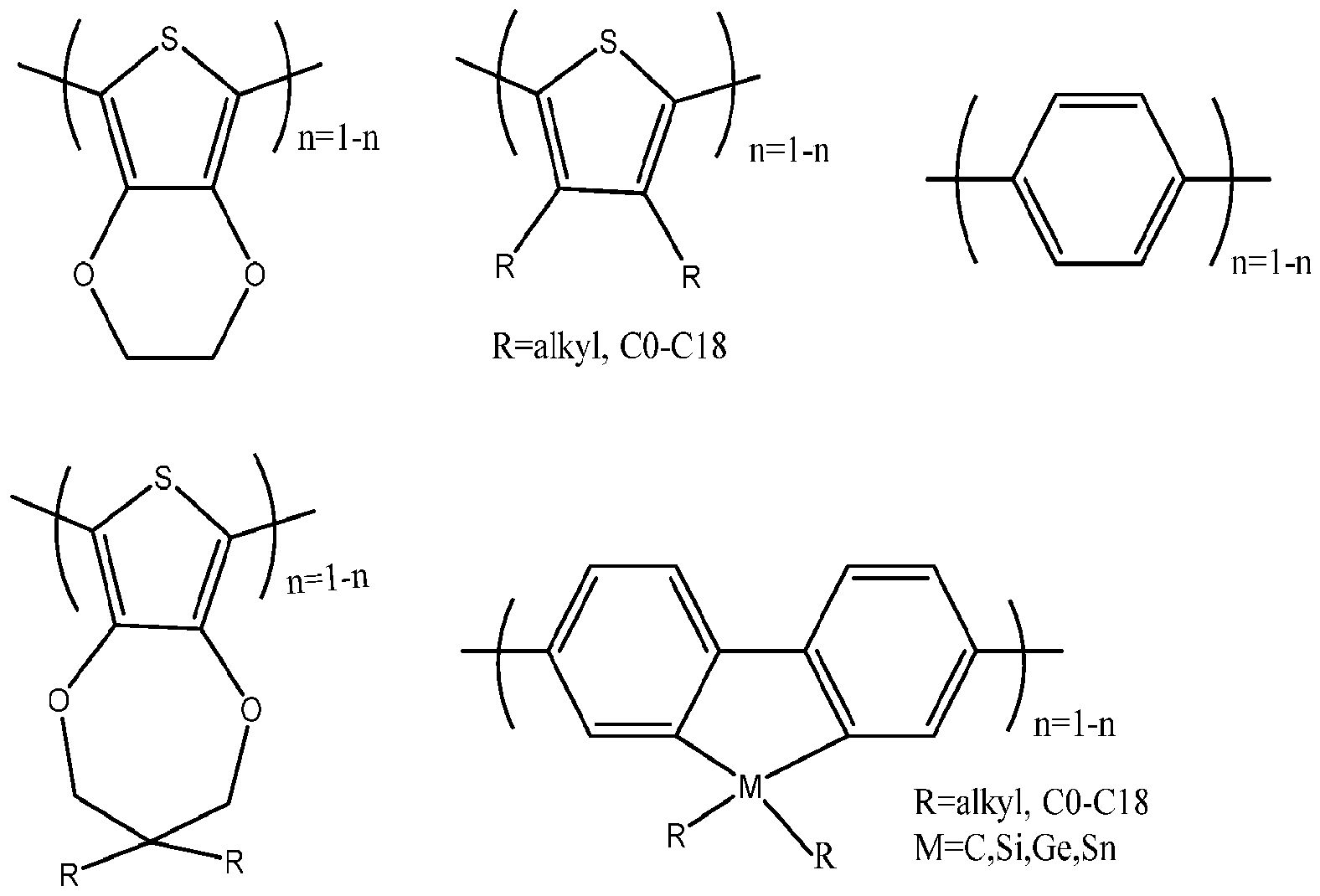
- X is selected from one of the following polymeric compounds: where Ar is
- An optoelectronic semiconductor can include an electron transporting material (ETM) infiltrated with a perovskite absorbing material and a coating of the dispiro-oxepine derivative according to the present subject matter disposed on the ETM.
- ETM electron transporting material
- Fig. 1 is a reaction scheme for the synthesis of dispiro-oxepine derivatives as a single molecule or monomeric form for optoelectronic semiconductors, also referred to herein as DTDOF.
- Fig. 2 is an alternative reaction scheme for the synthesis of dispiro-oxepine derivatives as a polymeric form for optoelectronic semiconductors, also referred to herein as Poly-DTDOF.
- the dispiro-oxepine derivatives for optoelectronic semiconductors provide compounds that serve as an efficient hole transporting material when applied as a coating on an electron transporting material infiltrated with a perovskite absorbing material to form semiconductors for perovskite solar cells and other optoelectronic devices.
- the dispiro- oxepine derivatives also referred to as "DTDOF” and “poly-DTDOF” herein, can include a dispiro-tri-dithienoe-oxepine-flourene (DTDOF) moiety.
- the dispiro-oxepine derivatives include a compound of Formula I (DTDOF), Formula II (Poly-DTDOF), and Formula III (DDOF), shown below:
- R is hydrogen, C1-C18 alkyl, C1-C18 perfluoroalkyl, or
- a dispiro-oxepine derivative for optoelectronic semiconductors includes a polymeric compound of formula (II):
- X is selected from one of the following polymeric compounds:
- a dispiro-oxepine derivative for optoelectronic semiconductors includes a compound of formula (III):
- Hole transport material refers to any material or composition wherein charges are transported by electron or hole movement (electronic motion) across the material or composition.
- the “hole transport material” is thus an electrically conductive material.
- Such hole transport materials, etc. are different from electrolytes, as charges are transported by diffusion of molecules in electrolytes.
- perovskite refers to the “perovskite structure” and not specifically to the perovskite material, CaTi0 3 .
- perovskite encompasses and preferably relates to any material that has the same type of crystal structure as calcium titanium oxide and other materials in which the bivalent cation is replaced by two separate monovalent cations.
- the dispiro-oxepine derivatives for optoelectronic semiconductors provide a hole transporting material comprising at least one compound selected from the group consisting of a compound according to Formula I, a compound according to Formula II, and a compound according to Formula III.
- the dispiro-oxepine derivatives for optoelectronic semiconductors may be used to make an optoelectronic and/or photoelectrochemical device.
- the optoelectronic and/or photoelectrochemical device may be an organic photovoltaic device, a lasing device, a light emitting device, a photo detection device, a photovoltaic solid state device, a p-n heterojunction, silicon tandem solar cell, an organic solar cell, a dye sensitized solar cell, a solid state solar cell, a phototransistor, or an OLED.
- the optoelectronic and/or photoelectrochemical device may be a solid-state solar cell comprising an organic-inorganic perovskite as sensitizer under the form of a layer.
- the dispiro-oxepine derivatives for optoelectronic semiconductors can be used as a tuner of a HOMO level based on the presence of thiophene groups.
- the dispiro-oxepine derivatives with and without dopant can provide both effective charge extraction (HTM function) and photocurrent enhancement (passivation of the perovskite layer, good electron transmission performance and cavity transmission performance) in a solid-state photovoltaic device and improve the PCE of optoelectronic and/or photoelectrochemical devices, particularly optoelectronic and/or photoelectrochemical devices comprising perovskite pigment as a sensitizer.
- HTM function effective charge extraction
- photocurrent enhancement passivation of the perovskite layer, good electron transmission performance and cavity transmission performance
- the optoelectronic and/or photoelectrochemical device may have a conducting support layer, a surface-increasing scaffold structure, an n-type semiconductor, a light- harvester layer or a sensitizer layer, a hole transporting layer, and a counter electrode and/or metal layer.
- the metal layer may be doped, as well as the n-type semiconductor.
- a conductive layer comprising a conductive material may be present between the hole transporting layer and the counter electrode and/or metal layer.
- the hole transporting layer may be provided on the sensitizer layer and is between the sensitizer layer and the conducting current providing layer, if present, or the counter electrode and/or metal layer. Further layers may be present.
- the optoelectronic and/or photoelectrochemical device may comprise a combination of two or more compounds of the dispiro-oxepine derivatives for optoelectronic semiconductors as hole transporting material.
- the hole transporting layer may comprise the combination of two or more compounds.
- the optoelectronic and/or photoelectrochemical device may comprise a hole collector layer, a conductive layer, an electron blocking layer, a sensitizer layer and a current collector layer, wherein the hole collector layer is coated by the conductive layer; and wherein the electron blocking layer is between the conductive layer and the sensitizer layer, which is in contact with the current collector layer.
- the hole collector layer comprises a hole transporting material comprising at least one compound of the dispiro-oxepine derivatives for optoelectronic semiconductors according to Formula I, Formula II , and/or Formula III.
- the conductive material may be selected from one or more conductive polymers or one or more hole transporting materials.
- examples of such materials may include poly(3,4- ethylenedioxythiophene) :poly(styrenesulfonate) (PEDOT:PS S) , poly(3 ,4- ethylenedioxythiophene):poly(styrenesulfonate):grapheme nanocomposite (PEDOT:PSS:graphene), poly(N-vinylcarbazole) (PVK) and sulfonated poly(diphenylamine) (SPDPA), preferably PEDOT:PSS, PEDOT:PSS:graphene and PVK, more preferably PEDOT:PSS.
- PEDOT:PS S poly(3,4- ethylenedioxythiophene) :poly(styrenesulfonate)
- PVK poly(N-vinylcarbazole)
- SPDPA sulfonated poly(
- Suitable conductive polymers may include polyaniline, polypyrrole, polythiophene, polybenzene, polyethylenedioxythiophene, polypropylenedioxy-thiophene, polyacetylene, and combinations of two or more of the aforementioned, for example.
- a transparent polymer film may be used, such as tetraacetyl cellulose (TAC), polyethylene tereph-thalate (PET), polyethylene naphthalate (PEN), syndiotactic polystyrene (SPS), polyphe-nylenesulfide (PPS), polycarbonate (PC), polyarylate (PAr), polysulfone (PSF), polyestersulfone (PES), polyimide (PI), polyetherimide (PEI), polycycloolefin such as polynorbornene, or brominated phenoxy resin.
- TAC tetraacetyl cellulose
- PET polyethylene tereph-thalate
- PEN polyethylene naphthalate
- SPS syndiotactic polystyrene
- PPS polyphe-nylenesulfide
- PC polycarbonate
- PAr polyarylate
- PSF polysulfone
- PSF polyestersulfone
- Transparent means transparent to at least a part, preferably a major part, of the visible light.
- the conducting support layer is substantially transparent to all wavelengths or types of visible light.
- the conducting support layer may be transparent to non-visible light, such as UV and IR radiation.
- the conducting support layer may provide the support layer of a photovoltaic solid- state device.
- the optoelectronic and/or electrochemical device is built on the support layer.
- the support of the device may be also provided on the side of the counter electrode.
- the conductive support layer does not necessarily provide the support of the device, but may simply be or comprise a current collector, for example, a metal foil.
- the conducting support layer preferably functions and/or comprises a current collector, collecting the current obtained from the device.
- the conducting support layer may comprise a material selected from indium-doped tin oxide (ITO), fluorine-doped tin oxide (FTO), ZnO-Ga 2 (3 ⁇ 4, ⁇ - ⁇ 2 ⁇ 3 , tin oxide, antimony-doped tin oxide (ATO), SrGe0 3 and zinc oxide, preferably coated on a transparent substrate, such as plastic or glass.
- the plastic or glass provides the support structure of the layer, and the cited conducting material provides the conductivity.
- Such support layers are generally known as conductive glass and conductive plastic, respectively, which are thus preferred conducting support layers.
- the conducting support layer comprises a conducting transparent layer, which may be selected from conducting glass and from conducting plastic.
- Suitable inorganic electron-transport materials are semi-conductive metal oxides, including oxides of titanium, tin, zinc, iron, tungsten, zirconium, hafnium, strontium, indium, cerium, yttrium, lanthanum, vanadium, cesium, niobium or tantalum. Furthermore, oxide- based semiconductors, such as may be used, wherein M and M are,
- a metal atom independently of each other, a metal atom, O is an oxygen atom, and x, y, and z are numbers (including 0). Examples are
- These semiconducting metal oxides can act as a scaffold structure in the solar cell.
- the surface-increasing scaffold structure is provided on the conducting support structure or on a protective layer that may be provided on the scaffold structure.
- the surface- increasing scaffold structure is nanostructured and/or mesoporous.
- the scaffold structure is made from and/or comprises a metal oxide.
- the material of the scaffold structure is selected from semiconducting materials, such as Si, Ti0 2 , GaP, InP, GaAs, CuInS 2 , CuInSe 2 , and combinations thereof.
- Preferred semiconductor materials are Si, Ti0 2 , Sn0 2 , ZnO, W0 3 , Nb 2 0 5 , and SrTi0 3 , for example.
- intermediate layers between the scaffold structure and the conductive support.
- Such intermediate layers if present, would preferably be conducting and/or semiconducting.
- the sensitizer layer of the optoelectronic and/or photoelectrochemical device comprises at least one pigment, which may be organic, inorganic, organometallic and organic-inorganic pigments, or a combination thereof.
- the sensitizer is preferably a light absorbing compound or material.
- the sensitizer is a pigment, and most preferably the sensitizer is an organic-inorganic pigment.
- the sensitizer layer or light-harvester layer may comprise one or more pigments of the group consisting of organometallic sensitizing compounds (phthalocyanine derived compounds, porphyrine derived compounds), metal-free organic sensitizing compounds (diketopyrrolopyrrole (DPP)-based sensitizer), inorganic sensitizing compounds such as quantum dots, Sb 2 S 3 (Antimony sulfide, for example in the form of thin films), aggregates of organic pigments, nanocomposites, in particular, organic-inorganic perovskites, and combinations of the aforementioned.
- organometallic sensitizing compounds phthalocyanine derived compounds, porphyrine derived compounds
- metal-free organic sensitizing compounds diketopyrrolopyrrole (DPP)-based sensitizer
- inorganic sensitizing compounds such as quantum dots, Sb 2 S 3 (Antimony sulfide, for example in the form of thin films), aggregates of organic pigments, nanocomposites, in particular, organic-in
- the optoelectronic and/or photoelectrochemical device may be selected from a photovoltaic solid-state device or a solar cell comprising an organic-inorganic perovskite as sensitizer under the form of a layer.
- the perovskite structure has the general stoichiometry WMX 3 , where "W” and “M” are cations, and "X" is an anion.
- the "W” and "M” cations can have a variety of charges, and in the original Perovskite mineral (CaTi0 3 ), the W cation is divalent and the M cation is tetravalent.
- the light-harvester layer or the sensitizer layer may comprise, or consist of, or be made of an organic-inorganic perovskite.
- the organic-inorganic perovskite is provided under a film of one perovskite pigment or mixed perovskite pigments or perovskite pigments mixed with further dyes or sensitizers.
- the sensitizer layer may comprise a further pigment in addition to the organic-inorganic perovskite pigment, the further pigment selected from an organic pigment, an organometallic pigment, or an inorganic pigment.
- the perovskite formulae may include structures having three (3) or four (4) anions, which may be the same or different, and/or one or two (2) organic cations, and/or metal atoms carrying two or three positive charges, in accordance with the formulae presented elsewhere herein.
- Photovoltaic technology is one of the most effective approaches to utilize solar energy, which directly converts sunlight into electricity.
- the dispiro-oxepine derivatives for optoelectronic semiconductors also provide a new hole transporting material allowing tuning of the HOMO level and having a positive impact on the sensitizer through its passivation to improve and provide higher PCE to photovoltaic devices comprising perovskite, as well as to other optoelectronic devices, for example, Organic Light Emitting Diodes (OLED) and Field Effect Transistors (FET).
- OLED Organic Light Emitting Diodes
- FET Field Effect Transistors
- the dispiro-oxepine derivatives for optoelectronic semiconductors provide an efficient solar cell, which can be rapidly prepared in an efficient way, using readily available or low-cost materials, such as conductive material, and using a short manufacturing procedure based on industrially known manufacturing steps, keeping the material costs and the material impact on the environment very low.
- the dispiro-oxepine derivatives for optoelectronic semiconductors relate to certain organic compounds, as well as their use as hole transport materials with and without dopant.
- these compounds may be used to tune HOMO levels in optoelectronic and/or electrochemical devices, such as lasing, light emitting devices, and can be used for photo detection, particularly in solar cells and solid-state solar cells, including tandem cell applications comprising these compounds.
- the dispiro-oxepine derivatives for optoelectronic semiconductors may be used as hole transporting material and may function as hole injection materials to bring holes extracted from a sensitizer to the hole collector of a photovoltaic device, e.g., a solid solar cell.
- the dispiro-oxepine derivatives for optoelectronic semiconductors are able to passivate the sensitizer or the sensitizer layer and to improve the performance and the efficiency of such a device, and in particular an optoelectronic and/or photoelectrochemical device comprising an organic-inorganic perovskite as sensitizer.
- dispiro-oxepine derivatives for optoelectronic semiconductors of Formula I, Formula ⁇ , and Formula III can be synthesized using the synthetic routes depicted Figs. 1 and 2.
- Perovskite solar cells including one or more of the dispiro-oxepine derivatives of Formula I, Formula II, and Formula III can provide a power conversion efficiency (PCE) value of greater than about 20%, and a stability of greater than about 500 hours, e.g., over 1000 hours.
- PCE power conversion efficiency
- the dispiro-oxepine derivatives for optoelectronic semiconductors of Formula I, Formula II, and Formula III can be a low cost HTM and a suitable replacement for spiro-OMeTAD.
- the HTM materials were prepared in accordance with the reaction scheme provided in Fig. 2.
- Compound 1 was dissolved in dry THF under nitrogen and n-BuLi was added dropwise at -78 °C. After 30 minutes of stirring, trimethyl tin chloride was added slowly at - 78 °C, then warmed to room temperature, extracted with ether, and dried in MgS0 4 to obtain compound 2.
- Compound 2, without purification, was used for the next reaction.
- Compounds 2 and 3, and Pd catalyst in dry toluene were degassed and refluxed under nitrogen for 1 day, then warmed, extracted, and dried over MgS0 4 . The obtained compound 4 was further purified by column chromatography, Yield 60%.
- dispiro-oxepine derivatives for optoelectronic semiconductors are not limited to the specific embodiments described above, but encompasses any and all embodiments within the scope of the generic language of the following claims enabled by the embodiments described herein, or otherwise shown in the drawings or described above in terms sufficient to enable one of ordinary skill in the art to make and use the claimed dispiro-oxepine derivatives for optoelectronic semiconductors.
Landscapes
- Physics & Mathematics (AREA)
- Spectroscopy & Molecular Physics (AREA)
- Chemical & Material Sciences (AREA)
- Engineering & Computer Science (AREA)
- Materials Engineering (AREA)
- Photovoltaic Devices (AREA)
Abstract
The dispiro-oxepine derivative for optoelectronic semiconductors includes compounds having the formula (I): where R is hydrogen, C1-C18 alkyl, C1-C18 perfluoroalkyl, or (CH2) n -(CF2) n -F where n=1-18; and where Ar is p-MeOC6H4, p-MeSC6H4, phenyl, p-C6H13OC6H4, p-C6H13SC6H4, p-MeC6H4, or p-PhC6H4. Compounds of the above formula serve as efficient hole transporting materials when applied as a coating on an electron transporting material infiltrated with a perovskite absorbing material to form semiconductors for perovskite solar cells and other optoelectronic devices.
Description
DISPIRO-OXEPINE DERIVATIVES FOR
OPTOELECTRONIC SEMICONDUCTORS
TECHNICAL FIELD
The disclosure of the present patent application relates to optoelectronic semiconductors, and particularly to dispiro-oxepine derivatives for optoelectronic semiconductors that serve as an efficient hole transporting material when applied as a coating on an electron transporting material infiltrated with a perovskite absorbing material to form semiconductors for perovskite solar cells and other optoelectronic devices.
BACKGROUND ART The conversion of solar energy to electrical current using thin film third generation photovoltaics (PV) has been widely explored for the last two decades. The sandwich/monolithic-type PV devices, consisting of a mesoporous photoanode with an organic/inorganic light harvester, redox electrolyte/solid- state hole conductor, and counter electrode, have attracted significant interest due to the ease of their fabrication, their flexibility in the selection of materials, and their low cost effective production.
In recent years, perovskite-based solar cells (PSCs) have become particularly appealing in the photovoltaics field, since they have inexpensive precursors, simple fabrication methods, and remarkably high power conversion efficiency (PCE) values. A typical PSC configuration is composed of an electron transporting material (ETM), which is infiltrated with the perovskite absorbing material and coated with a hole transporting material (HTM), which plays an important role to facilitate the movement of holes from perovskite to the counter electrode.
Perovskite-based and other types of solid state solar cells generally contain an organic HTM layer for transporting holes created by charge separation at the light harvester to the counter electrode and/or cathode for filling up with incoming electrons, thereby closing the electric circuit and rendering the devices regenerative.
Spiro-based organic semiconductors have attracted considerable attention, more precisely, 2,2' ,7,7'-tetrakis-(N,N-di-4-methoxyphenylamine)-9,9'-spirobifluorene (spiro- OMeTAD) has been selected as the benchmark HTM for PSC. Currently, most performing solid-state devices use doped spiro-OMeTAD as a HTM. The relatively low PCE of solid- state devices was often ascribed to the low hole mobility in spiro-OMeTAD, which causes interfacial recombination losses by two orders of magnitude higher than in electrolyte-based,
dye-sensitized solar cells (DSCCs).
Further, the use of spiro-OMeTAD as a hole transporting material may trigger instability in such solid-state solar cells. Because spiro-OMeTAD has two oxidation potentials that are close, this HTM in the oxidized form is able to form a di-cation, which, in turn, can dismutate and might cause device instability. Further, since spiro-OMeTAD is present in a semi-crystalline form, there is the risk that it will (re)crystallize in the processed form in the solar cell. In addition, solubility in customary process solvents is relatively low, which leads to a correspondingly low degree of pore filling. Along with stability issues, the high cost due to a complicated synthetic route and the high purity that is required (sublimation grade) in order to have good performance have been the main drawbacks for commercial applications of solid-state solar cells.
Due to the tedious multi-step synthesis of spiro-OMeTAD, which makes it prohibitively expensive and cost-ineffective, as well as the necessary high-purity sublimation-grade spiro-OMeTAD required to obtain high-performance devices, there is a huge interest in development of novel small-molecule organic semiconductors.
As such, there have been attempts to find an alternate organic HTM having higher charge carrier mobility and matching HOMO (highest occupied molecular orbital) level to replace spiro-OMeTAD. So far, although a large number and different types of HTMs were reported reaching efficiency of 16-19%, only very few candidates have showed PCE values over 19%, mainly because of the additional interaction associated with improving the hole transfer at the HTM/perovskite interface.
Thus, dispiro-oxepine/dispiro-thiamine derivatives for optoelectronic semiconductors solving the aforementioned problems are desired.
DISCLOSURE OF INVENTION According to an embodiment, a dispiro-oxepine derivative for optoelectronic semiconductors includes a compound of formula (I):


where «=1-18; and wher
According to an embodiment, a dispiro-oxepine derivative for optoelectronic semiconductors includes a polymeric compound of formula (II):

where X is selected from one of the following polymeric compounds:
 where Ar is
An optoelectronic semiconductor can include an electron transporting material (ETM) infiltrated with a perovskite absorbing material and a coating of the dispiro-oxepine derivative according to the present subject matter disposed on the ETM.
These and other features of the present disclosure will become readily apparent upon further review of the following specification and drawings.
BRIEF DESCRIPTION OF THE DRAWINGS
Fig. 1 is a reaction scheme for the synthesis of dispiro-oxepine derivatives as a single molecule or monomeric form for optoelectronic semiconductors, also referred to herein as DTDOF.
Fig. 2 is an alternative reaction scheme for the synthesis of dispiro-oxepine derivatives as a polymeric form for optoelectronic semiconductors, also referred to herein as Poly-DTDOF. BEST MODE(S) FOR CARRYING OUT THE INVENTION
The dispiro-oxepine derivatives for optoelectronic semiconductors provide compounds that serve as an efficient hole transporting material when applied as a coating on an electron transporting material infiltrated with a perovskite absorbing material to form semiconductors for perovskite solar cells and other optoelectronic devices. The dispiro- oxepine derivatives, also referred to as "DTDOF" and "poly-DTDOF" herein, can include a dispiro-tri-dithienoe-oxepine-flourene (DTDOF) moiety. The dispiro-oxepine derivatives include a compound of Formula I (DTDOF), Formula II (Poly-DTDOF), and Formula III (DDOF), shown below:

where «=1-18; and where Ar i

According to an embodiment, a dispiro-oxepine derivative for optoelectronic semiconductors includes a polymeric compound of formula (II):

where X is selected from one of the following polymeric compounds:

According to an embodiment, a dispiro-oxepine derivative for optoelectronic semiconductors includes a compound of formula (III):

Formula III
where Ar is

"Hole transport material", "hole transporting material", "charge transporting material", "organic hole transport material", "inorganic hole transport material", and the like as used herein, refer to any material or composition wherein charges are transported by electron or hole movement (electronic motion) across the material or composition. The "hole transport material" is thus an electrically conductive material. Such hole transport materials, etc., are different from electrolytes, as charges are transported by diffusion of molecules in electrolytes.
The term "perovskite", as used herein, refers to the "perovskite structure" and not specifically to the perovskite material, CaTi03. As used herein, "perovskite" encompasses and preferably relates to any material that has the same type of crystal structure as calcium titanium oxide and other materials in which the bivalent cation is replaced by two separate monovalent cations.
The dispiro-oxepine derivatives for optoelectronic semiconductors provide a hole transporting material comprising at least one compound selected from the group consisting of a compound according to Formula I, a compound according to Formula II, and a compound according to Formula III. The dispiro-oxepine derivatives for optoelectronic semiconductors may be used to make an optoelectronic and/or photoelectrochemical device. The optoelectronic and/or photoelectrochemical device may be an organic photovoltaic device, a lasing device, a light emitting device, a photo detection device, a photovoltaic solid state device, a p-n heterojunction, silicon tandem solar cell, an organic solar cell, a dye sensitized solar cell, a solid state solar cell, a phototransistor, or an OLED. The optoelectronic and/or photoelectrochemical device may be a solid-state solar cell comprising an organic-inorganic perovskite as sensitizer under the form of a layer. The dispiro-oxepine derivatives for optoelectronic semiconductors can be used as a tuner of a HOMO level based on the presence of thiophene groups.
The dispiro-oxepine derivatives with and without dopant can provide both effective charge extraction (HTM function) and photocurrent enhancement (passivation of the perovskite layer, good electron transmission performance and cavity transmission performance) in a solid-state photovoltaic device and improve the PCE of optoelectronic and/or photoelectrochemical devices, particularly optoelectronic and/or photoelectrochemical devices comprising perovskite pigment as a sensitizer.
The optoelectronic and/or photoelectrochemical device may have a conducting
support layer, a surface-increasing scaffold structure, an n-type semiconductor, a light- harvester layer or a sensitizer layer, a hole transporting layer, and a counter electrode and/or metal layer. The metal layer may be doped, as well as the n-type semiconductor. A conductive layer comprising a conductive material may be present between the hole transporting layer and the counter electrode and/or metal layer. The hole transporting layer may be provided on the sensitizer layer and is between the sensitizer layer and the conducting current providing layer, if present, or the counter electrode and/or metal layer. Further layers may be present.
The optoelectronic and/or photoelectrochemical device may comprise a combination of two or more compounds of the dispiro-oxepine derivatives for optoelectronic semiconductors as hole transporting material. The hole transporting layer may comprise the combination of two or more compounds.
The optoelectronic and/or photoelectrochemical device may comprise a hole collector layer, a conductive layer, an electron blocking layer, a sensitizer layer and a current collector layer, wherein the hole collector layer is coated by the conductive layer; and wherein the electron blocking layer is between the conductive layer and the sensitizer layer, which is in contact with the current collector layer. The hole collector layer comprises a hole transporting material comprising at least one compound of the dispiro-oxepine derivatives for optoelectronic semiconductors according to Formula I, Formula II , and/or Formula III.
The conductive material may be selected from one or more conductive polymers or one or more hole transporting materials. Examples of such materials may include poly(3,4- ethylenedioxythiophene) :poly(styrenesulfonate) (PEDOT:PS S) , poly(3 ,4- ethylenedioxythiophene):poly(styrenesulfonate):grapheme nanocomposite (PEDOT:PSS:graphene), poly(N-vinylcarbazole) (PVK) and sulfonated poly(diphenylamine) (SPDPA), preferably PEDOT:PSS, PEDOT:PSS:graphene and PVK, more preferably PEDOT:PSS. Other suitable conductive polymers may include polyaniline, polypyrrole, polythiophene, polybenzene, polyethylenedioxythiophene, polypropylenedioxy-thiophene, polyacetylene, and combinations of two or more of the aforementioned, for example. Alternatively, a transparent polymer film may be used, such as tetraacetyl cellulose (TAC), polyethylene tereph-thalate (PET), polyethylene naphthalate (PEN), syndiotactic polystyrene (SPS), polyphe-nylenesulfide (PPS), polycarbonate (PC), polyarylate (PAr), polysulfone (PSF), polyestersulfone (PES), polyimide (PI), polyetherimide (PEI), polycycloolefin such as polynorbornene, or brominated phenoxy resin. Polymer films are preferred, in particular PET, PEN, and polynorbornene.
The conducting support layer is preferably substantially transparent. "Transparent" means transparent to at least a part, preferably a major part, of the visible light. Preferably, the conducting support layer is substantially transparent to all wavelengths or types of visible light. Furthermore, the conducting support layer may be transparent to non-visible light, such as UV and IR radiation.
The conducting support layer may provide the support layer of a photovoltaic solid- state device. Preferably, the optoelectronic and/or electrochemical device is built on the support layer. The support of the device may be also provided on the side of the counter electrode. In this case, the conductive support layer does not necessarily provide the support of the device, but may simply be or comprise a current collector, for example, a metal foil.
The conducting support layer preferably functions and/or comprises a current collector, collecting the current obtained from the device. The conducting support layer may comprise a material selected from indium-doped tin oxide (ITO), fluorine-doped tin oxide (FTO), ZnO-Ga2(¾, ΖηΟ-Αΐ2θ3, tin oxide, antimony-doped tin oxide (ATO), SrGe03 and zinc oxide, preferably coated on a transparent substrate, such as plastic or glass. In this case, the plastic or glass provides the support structure of the layer, and the cited conducting material provides the conductivity. Such support layers are generally known as conductive glass and conductive plastic, respectively, which are thus preferred conducting support layers. The conducting support layer comprises a conducting transparent layer, which may be selected from conducting glass and from conducting plastic.
Suitable inorganic electron-transport materials are semi-conductive metal oxides, including oxides of titanium, tin, zinc, iron, tungsten, zirconium, hafnium, strontium, indium, cerium, yttrium, lanthanum, vanadium, cesium, niobium or tantalum. Furthermore, oxide- based semiconductors, such as may be used, wherein M and M are,

independently of each other, a metal atom, O is an oxygen atom, and x, y, and z are numbers (including 0). Examples are
and zinc stannate. These semiconducting metal oxides can act as a scaffold structure in the solar cell.
The surface-increasing scaffold structure is provided on the conducting support structure or on a protective layer that may be provided on the scaffold structure. The surface- increasing scaffold structure is nanostructured and/or mesoporous.
The scaffold structure is made from and/or comprises a metal oxide. For example, the material of the scaffold structure is selected from semiconducting materials, such as Si, Ti02,
 GaP, InP, GaAs, CuInS2, CuInSe2, and combinations thereof. Preferred semiconductor materials are Si, Ti02, Sn02, ZnO, W03, Nb205, and SrTi03, for example.
There may be one or more intermediate layers between the scaffold structure and the conductive support. Such intermediate layers, if present, would preferably be conducting and/or semiconducting.
The sensitizer layer of the optoelectronic and/or photoelectrochemical device comprises at least one pigment, which may be organic, inorganic, organometallic and organic-inorganic pigments, or a combination thereof. The sensitizer is preferably a light absorbing compound or material. Preferably, the sensitizer is a pigment, and most preferably the sensitizer is an organic-inorganic pigment.
The sensitizer layer or light-harvester layer may comprise one or more pigments of the group consisting of organometallic sensitizing compounds (phthalocyanine derived compounds, porphyrine derived compounds), metal-free organic sensitizing compounds (diketopyrrolopyrrole (DPP)-based sensitizer), inorganic sensitizing compounds such as quantum dots, Sb2S3 (Antimony sulfide, for example in the form of thin films), aggregates of organic pigments, nanocomposites, in particular, organic-inorganic perovskites, and combinations of the aforementioned.
The optoelectronic and/or photoelectrochemical device may be selected from a photovoltaic solid-state device or a solar cell comprising an organic-inorganic perovskite as sensitizer under the form of a layer. The perovskite structure has the general stoichiometry WMX3, where "W" and "M" are cations, and "X" is an anion. The "W" and "M" cations can have a variety of charges, and in the original Perovskite mineral (CaTi03), the W cation is divalent and the M cation is tetravalent.
The light-harvester layer or the sensitizer layer may comprise, or consist of, or be made of an organic-inorganic perovskite. The organic-inorganic perovskite is provided under a film of one perovskite pigment or mixed perovskite pigments or perovskite pigments mixed with further dyes or sensitizers. The sensitizer layer may comprise a further pigment in addition to the organic-inorganic perovskite pigment, the further pigment selected from an organic pigment, an organometallic pigment, or an inorganic pigment. The perovskite formulae may include structures having three (3) or four (4) anions, which may be the same or different, and/or one or two (2) organic cations, and/or metal atoms carrying two or three positive charges, in accordance with the formulae presented elsewhere herein.
Photovoltaic technology is one of the most effective approaches to utilize solar energy, which directly converts sunlight into electricity. The dispiro-oxepine derivatives for
optoelectronic semiconductors also provide a new hole transporting material allowing tuning of the HOMO level and having a positive impact on the sensitizer through its passivation to improve and provide higher PCE to photovoltaic devices comprising perovskite, as well as to other optoelectronic devices, for example, Organic Light Emitting Diodes (OLED) and Field Effect Transistors (FET).
The dispiro-oxepine derivatives for optoelectronic semiconductors provide an efficient solar cell, which can be rapidly prepared in an efficient way, using readily available or low-cost materials, such as conductive material, and using a short manufacturing procedure based on industrially known manufacturing steps, keeping the material costs and the material impact on the environment very low.
The dispiro-oxepine derivatives for optoelectronic semiconductors relate to certain organic compounds, as well as their use as hole transport materials with and without dopant. In this regard, these compounds may be used to tune HOMO levels in optoelectronic and/or electrochemical devices, such as lasing, light emitting devices, and can be used for photo detection, particularly in solar cells and solid-state solar cells, including tandem cell applications comprising these compounds. The dispiro-oxepine derivatives for optoelectronic semiconductors may be used as hole transporting material and may function as hole injection materials to bring holes extracted from a sensitizer to the hole collector of a photovoltaic device, e.g., a solid solar cell. The dispiro-oxepine derivatives for optoelectronic semiconductors are able to passivate the sensitizer or the sensitizer layer and to improve the performance and the efficiency of such a device, and in particular an optoelectronic and/or photoelectrochemical device comprising an organic-inorganic perovskite as sensitizer.
The dispiro-oxepine derivatives for optoelectronic semiconductors of Formula I, Formula Π, and Formula III can be synthesized using the synthetic routes depicted Figs. 1 and 2.
Perovskite solar cells including one or more of the dispiro-oxepine derivatives of Formula I, Formula II, and Formula III can provide a power conversion efficiency (PCE) value of greater than about 20%, and a stability of greater than about 500 hours, e.g., over 1000 hours. For example, compounds of Formula I (where R=H) can provide a PCE that is greater than 20%. Compounds of Formula I (where R=C1-C18) can have a stability that is greater than 500 hours. The dispiro-oxepine derivatives for optoelectronic semiconductors of Formula I, Formula II, and Formula III can be a low cost HTM and a suitable replacement for spiro-OMeTAD.
The dispiro-oxepine derivatives for optoelectronic semiconductors will now be
illustrated by the following example, which do not limit the scope defined by the appended claims.
Example 1
Synthetic route for preparing dispiro-oxepine derivatives (Compound DTDOF) The dispiro-oxepine derivatives were prepared in accordance with the reaction scheme provided in Fig. 1. To a solution of compound 1 l(equiv) in 50 mL of dry THF at - 78 °C under argon atmosphere, n-BuLi (2.1 equiv) was added dropwise. After 2 hours at the same temperature, 2,7-dibromofluorenone ( 2.5 equiv) in THF (50 mL) was added to the mixture dropwise, and the solution was warmed to room temperature and stirred overnight. The mixture was washed with water, extracted with DCM, and the combined organic phases were dried over MgSCU. The solvent was evaporated and the crude product was precipitated in ethanol to afford a white solid which was used in the next step without further purification. The obtained solid was dissolved in boiling acetic acid (100 mL), and 1 mL of concentrated hydrochloric acid were added. After refluxing for 2 hours, the mixture was washed with water and extracted with DCM, and the combined organic phases were dried over MgS04. This crude residue was purified by flash chromatography with pure 20 % DCM in hexane to afford compound 2 (1.4 g, 41%).
In a 50 mL Schlenk-tube, 400 mg of compound 2 (1 equiv), 560 mg commercially available 4,4'-dimethoxydiphenylamine (5 equiv), and 280 mg t-BuONa (6 equiv) were dissolved in 20 mL dry toluene and degassed for 20 minutes with N2. After the addition of 70 mg Pd2dba3 (0.075 mmol, 15%) and 70 mg Xphos (0.15 mmol, 30%), the reaction was refluxed overnight. The reaction was then diluted with DCM and flashed through a plug of MgS04 to remove inorganic salts and metallic palladium. This crude residue was purified by flash chromatography with 30% THF in hexane. Isolated compound was dissolved in THF and dropped into MeOH. The precipitate was collected by filtration, washed with MeOH and dried. 420 mg (60 % yield) of pale yellow solid was obtained to afford compound 3.
Example 2
Synthetic route for preparing Poly-DTDOF HTM materials
The HTM materials were prepared in accordance with the reaction scheme provided in Fig. 2. Compound 1 was dissolved in dry THF under nitrogen and n-BuLi was added dropwise at -78 °C. After 30 minutes of stirring, trimethyl tin chloride was added slowly at -
78 °C, then warmed to room temperature, extracted with ether, and dried in MgS04 to obtain compound 2. Compound 2, without purification, was used for the next reaction. Compounds 2 and 3, and Pd catalyst in dry toluene were degassed and refluxed under nitrogen for 1 day, then warmed, extracted, and dried over MgS04. The obtained compound 4 was further purified by column chromatography, Yield 60%.
It is to be understood that the dispiro-oxepine derivatives for optoelectronic semiconductors are not limited to the specific embodiments described above, but encompasses any and all embodiments within the scope of the generic language of the following claims enabled by the embodiments described herein, or otherwise shown in the drawings or described above in terms sufficient to enable one of ordinary skill in the art to make and use the claimed dispiro-oxepine derivatives for optoelectronic semiconductors.
Claims
1. A dispiro-oxepine derivative for optoelectronic semiconductors, comprising a compound of the formula:

where R is hydrogen, C1-C18 alkyl, C1-C18 perfluoroalkyl, or where

where Ar
2. The dispiro-oxepine derivative for optoelectronic semiconductors, according to claim 1, wherein
3. The dispiro-oxepine derivative for optoelectronic semiconductors, according to claim 1, wherein R= H.
4. A semiconductor material for optoelectronic devices, comprising:
an electron transporting material (ETM) infiltrated with a perovskite absorbing material; and
a coating disposed on the ETM material, the coating including the compound according to claim 1.
5. An optoelectronic device, comprising:
a hole collector layer;
a conductive layer;
an electron blocking layer;
a sensitizer layer; and
a current collector layer, wherein
the hole collector layer is coated by the conductive layer,
the electron blocking layer is between the conductive layer and the sensitizer layer, and
the hole collector layer includes at least one compound of the formula:


6. The optoelectronic device according to claim 5, wherein R= C1-C18 alkyl.
7. The optoelectronic device according to claim 5, wherein R= H.
8. A dispiro-oxepine derivative for optoelectronic semiconductors, comprising a polymeric compound of the formula:

where X is selected from one of the following polymeric compounds:

9. A semiconductor material for optoelectronic devices, comprising: an electron transporting material (ETM) infiltrated with a perovskite absorbing material; and
a coating disposed on the ETM material, the coating including the compound according to claim 8.
10. An optoelectronic device, comprising:
a hole collector layer;
a conductive layer;
an electron blocking layer;
a sensitizer layer; and
a current collector layer, wherein
the hole collector layer is coated by the conductive layer,
the electron blocking layer is between the conductive layer and the sensitizer layer, and
the hole collector layer includes at least one compound according to Claim 8.
11. A dispiro-oxepine derivative for optoelectronic semiconductors, comprising a compound of the formula:

12. A semiconductor material for optoelectronic devices, comprising:
an electron transporting material (ETM) infiltrated with a perovskite absorbing material; and
a coating disposed on the ETM material, the coating including the compound according to claim 11.
13. An optoelectronic device, comprising:
a hole collector layer;
a conductive layer;
an electron blocking layer;
a sensitizer layer; and
a current collector layer, wherein
the hole collector layer is coated by the conductive layer,
the electron blocking layer is between the conductive layer and the sensitizer layi the hole collector layer includes at least one compound according to Claim 11.
Applications Claiming Priority (2)
| Application Number | Priority Date | Filing Date | Title |
|---|---|---|---|
| US201762467781P | 2017-03-06 | 2017-03-06 | |
| US62/467,781 | 2017-03-06 |
Publications (1)
| Publication Number | Publication Date |
|---|---|
| WO2018165101A1 true WO2018165101A1 (en) | 2018-09-13 |
Family
ID=63449143
Family Applications (1)
| Application Number | Title | Priority Date | Filing Date |
|---|---|---|---|
| PCT/US2018/021058 WO2018165101A1 (en) | 2017-03-06 | 2018-03-06 | Dispiro-oxepine derivatives for optoelectronic semiconductors |
Country Status (1)
| Country | Link |
|---|---|
| WO (1) | WO2018165101A1 (en) |
Citations (2)
| Publication number | Priority date | Publication date | Assignee | Title |
|---|---|---|---|---|
| WO2004058911A2 (en) * | 2002-12-23 | 2004-07-15 | Covion Organic Semiconductors Gmbh | Organic electroluminescent element |
| WO2018009771A1 (en) * | 2016-07-07 | 2018-01-11 | Qatar Foundation For Education, Science And Community Development | Dispiro-oxepine/thiapine derivatives for optoelectronic semiconductors |
-
2018
- 2018-03-06 WO PCT/US2018/021058 patent/WO2018165101A1/en active Application Filing
Patent Citations (2)
| Publication number | Priority date | Publication date | Assignee | Title |
|---|---|---|---|---|
| WO2004058911A2 (en) * | 2002-12-23 | 2004-07-15 | Covion Organic Semiconductors Gmbh | Organic electroluminescent element |
| WO2018009771A1 (en) * | 2016-07-07 | 2018-01-11 | Qatar Foundation For Education, Science And Community Development | Dispiro-oxepine/thiapine derivatives for optoelectronic semiconductors |
Non-Patent Citations (3)
| Title |
|---|
| JEUX, V. ET AL.: "Synthesis of Spiro[cyclopenta[1,2-b:5,4-b']DiThiophene-4, 9'-Fluorenes] SDTF dissymmetrically functionalized", TETRAHEDRON LETTERS, vol. 56, 2015, pages 1383 - 1387, XP055235028 * |
| RAKSTYS, K. ET AL.: "A highly hindered bithiophene-functionalized dispiro- oxepine derivative as an efficient hole transporting material for perovskite solar cells", J. MATER. CHEM., vol. 4, 21 October 2016 (2016-10-21), pages 18259 - 18264, XP055450680 * |
| WANG, Y.-K. ET AL.: "Dopant-Free Spiro-Triphenylamine/Fluorene as Hole- Transporting Material for Perovskite Solar Cells with Enhanced Efficiency and Stability", ADVANCED FUNCTIONAL MATERIALS, vol. 26, no. 9, 2016, pages 1375 - 1381, XP055310441 * |
Similar Documents
| Publication | Publication Date | Title |
|---|---|---|
| Hamed et al. | Mixed halide perovskite solar cells: progress and challenges | |
| EP3044817B1 (en) | Inverted solar cell and process for producing the same | |
| KR101906017B1 (en) | Mixed halide perovskite compound, preparing method thereof, and solar cell comprising the same | |
| US20150200377A1 (en) | Organo metal halide perovskite heterojunction solar cell and fabrication thereof | |
| EP3094688B1 (en) | Hole transporting and light absorbing material for solid state solar cells | |
| US10038150B2 (en) | Metal complexes for use as dopants and other uses | |
| EP2903047A1 (en) | Hole transporting and light absorbing material for solid state solar cells | |
| KR102046110B1 (en) | An organic-inorganic hybrid perovskite, method for preparation thereof, and solar cell comprising the same | |
| Meng et al. | Configurable organic charge carriers toward stable perovskite photovoltaics | |
| CN107438597B (en) | Small molecule hole transport materials for optoelectronic and photoelectrochemical devices | |
| US10727414B2 (en) | Functional hole transport materials for optoelectronic and/or electrochemical devices | |
| US9908857B2 (en) | Method of producing benzo[1,2-B:4,5-B′]dithiophene and benzothiadiazole-based molecular complexes | |
| WO2017098455A1 (en) | Charge transporting material for optoelectronic and/or photoelectrochemical devices | |
| EP2682996A1 (en) | Thin film solar cell | |
| KR20210050288A (en) | Conjugated polymer for perovskite solar cell and perovskite solar cell comprising the same | |
| KR102121756B1 (en) | Perovskite solar cell, polymer for perovskite solar cell and method for manufacturing the same | |
| US20190334092A1 (en) | Dispiro-oxepine/thiapine derivatives for optoelectronic semiconductors | |
| WO2018165101A1 (en) | Dispiro-oxepine derivatives for optoelectronic semiconductors | |
| JP7172655B2 (en) | Photoelectric conversion elements, devices, and power supply modules | |
| KR101833215B1 (en) | Organic semiconducting compounds, manufacturing method thereof, and organic electronic device containing the same | |
| KR102319359B1 (en) | Inorganic-organic hybrid solar cell | |
| KR101799929B1 (en) | polymerized polymer from monomer of particular ratio and manufacturing method thereof and organic semiconductor device comprising the polymer | |
| KR102022688B1 (en) | A compound having 3-picoliniumylammonium as an absorber, method for preparation thereof, and solar cell comprising the same | |
| KR20160141541A (en) | Hole transfer material, method for preparation thereof, and solar cell comprising the same |
Legal Events
| Date | Code | Title | Description |
|---|---|---|---|
| 121 | Ep: the epo has been informed by wipo that ep was designated in this application |
Ref document number: 18763982 Country of ref document: EP Kind code of ref document: A1 |
|
| NENP | Non-entry into the national phase |
Ref country code: DE |
|
| 122 | Ep: pct application non-entry in european phase |
Ref document number: 18763982 Country of ref document: EP Kind code of ref document: A1 |