EP3044817B1 - Inverted solar cell and process for producing the same - Google Patents
Inverted solar cell and process for producing the same Download PDFInfo
- Publication number
- EP3044817B1 EP3044817B1 EP14767143.2A EP14767143A EP3044817B1 EP 3044817 B1 EP3044817 B1 EP 3044817B1 EP 14767143 A EP14767143 A EP 14767143A EP 3044817 B1 EP3044817 B1 EP 3044817B1
- Authority
- EP
- European Patent Office
- Prior art keywords
- layer
- organic
- deposition
- perovskite
- sensitizer
- Prior art date
- Legal status (The legal status is an assumption and is not a legal conclusion. Google has not performed a legal analysis and makes no representation as to the accuracy of the status listed.)
- Active
Links
- 238000000034 method Methods 0.000 title claims description 65
- 230000008569 process Effects 0.000 title description 14
- 230000000903 blocking effect Effects 0.000 claims description 87
- 229910052751 metal Inorganic materials 0.000 claims description 65
- 239000002184 metal Substances 0.000 claims description 65
- 239000000463 material Substances 0.000 claims description 64
- -1 Ge2+ Chemical compound 0.000 claims description 48
- 239000004020 conductor Substances 0.000 claims description 47
- 238000000151 deposition Methods 0.000 claims description 47
- 150000003839 salts Chemical class 0.000 claims description 47
- 125000005842 heteroatom Chemical group 0.000 claims description 39
- 150000001768 cations Chemical class 0.000 claims description 35
- 239000007787 solid Substances 0.000 claims description 30
- 230000008021 deposition Effects 0.000 claims description 25
- 125000004122 cyclic group Chemical group 0.000 claims description 23
- LGDCSNDMFFFSHY-UHFFFAOYSA-N 4-butyl-n,n-diphenylaniline Polymers C1=CC(CCCC)=CC=C1N(C=1C=CC=CC=1)C1=CC=CC=C1 LGDCSNDMFFFSHY-UHFFFAOYSA-N 0.000 claims description 22
- 238000004519 manufacturing process Methods 0.000 claims description 18
- XOLBLPGZBRYERU-UHFFFAOYSA-N tin dioxide Chemical compound O=[Sn]=O XOLBLPGZBRYERU-UHFFFAOYSA-N 0.000 claims description 18
- 229920000144 PEDOT:PSS Polymers 0.000 claims description 17
- 229910052757 nitrogen Inorganic materials 0.000 claims description 17
- MCEWYIDBDVPMES-UHFFFAOYSA-N [60]pcbm Chemical compound C123C(C4=C5C6=C7C8=C9C%10=C%11C%12=C%13C%14=C%15C%16=C%17C%18=C(C=%19C=%20C%18=C%18C%16=C%13C%13=C%11C9=C9C7=C(C=%20C9=C%13%18)C(C7=%19)=C96)C6=C%11C%17=C%15C%13=C%15C%14=C%12C%12=C%10C%10=C85)=C9C7=C6C2=C%11C%13=C2C%15=C%12C%10=C4C23C1(CCCC(=O)OC)C1=CC=CC=C1 MCEWYIDBDVPMES-UHFFFAOYSA-N 0.000 claims description 15
- 125000004433 nitrogen atom Chemical group N* 0.000 claims description 15
- 229910001887 tin oxide Inorganic materials 0.000 claims description 14
- XLOMVQKBTHCTTD-UHFFFAOYSA-N Zinc monoxide Chemical compound [Zn]=O XLOMVQKBTHCTTD-UHFFFAOYSA-N 0.000 claims description 12
- 150000003863 ammonium salts Chemical class 0.000 claims description 11
- 238000000859 sublimation Methods 0.000 claims description 11
- 230000008022 sublimation Effects 0.000 claims description 11
- 229920001609 Poly(3,4-ethylenedioxythiophene) Polymers 0.000 claims description 10
- 150000003867 organic ammonium compounds Chemical group 0.000 claims description 10
- 238000002207 thermal evaporation Methods 0.000 claims description 10
- 238000005240 physical vapour deposition Methods 0.000 claims description 8
- 229920003227 poly(N-vinyl carbazole) Polymers 0.000 claims description 8
- OKTJSMMVPCPJKN-UHFFFAOYSA-N Carbon Chemical compound [C] OKTJSMMVPCPJKN-UHFFFAOYSA-N 0.000 claims description 7
- 239000011248 coating agent Substances 0.000 claims description 7
- 238000000576 coating method Methods 0.000 claims description 7
- 239000011521 glass Substances 0.000 claims description 7
- 229920003023 plastic Polymers 0.000 claims description 7
- 239000004033 plastic Substances 0.000 claims description 7
- 229920001467 poly(styrenesulfonates) Polymers 0.000 claims description 7
- UJOBWOGCFQCDNV-UHFFFAOYSA-N 9H-carbazole Chemical compound C1=CC=C2C3=CC=CC=C3NC2=C1 UJOBWOGCFQCDNV-UHFFFAOYSA-N 0.000 claims description 6
- XMWRBQBLMFGWIX-UHFFFAOYSA-N C60 fullerene Chemical compound C12=C3C(C4=C56)=C7C8=C5C5=C9C%10=C6C6=C4C1=C1C4=C6C6=C%10C%10=C9C9=C%11C5=C8C5=C8C7=C3C3=C7C2=C1C1=C2C4=C6C4=C%10C6=C9C9=C%11C5=C5C8=C3C3=C7C1=C1C2=C4C6=C2C9=C5C3=C12 XMWRBQBLMFGWIX-UHFFFAOYSA-N 0.000 claims description 6
- 238000005229 chemical vapour deposition Methods 0.000 claims description 6
- 229910052731 fluorine Inorganic materials 0.000 claims description 6
- 229910021389 graphene Inorganic materials 0.000 claims description 6
- 229910052738 indium Inorganic materials 0.000 claims description 6
- 238000005092 sublimation method Methods 0.000 claims description 6
- 239000011787 zinc oxide Substances 0.000 claims description 6
- 238000010438 heat treatment Methods 0.000 claims description 5
- 229910044991 metal oxide Inorganic materials 0.000 claims description 5
- 150000004706 metal oxides Chemical class 0.000 claims description 5
- DCZNSJVFOQPSRV-UHFFFAOYSA-N n,n-diphenyl-4-[4-(n-phenylanilino)phenyl]aniline Chemical compound C1=CC=CC=C1N(C=1C=CC(=CC=1)C=1C=CC(=CC=1)N(C=1C=CC=CC=1)C=1C=CC=CC=1)C1=CC=CC=C1 DCZNSJVFOQPSRV-UHFFFAOYSA-N 0.000 claims description 5
- YCKRFDGAMUMZLT-UHFFFAOYSA-N Fluorine atom Chemical compound [F] YCKRFDGAMUMZLT-UHFFFAOYSA-N 0.000 claims description 4
- 229910007470 ZnO—Al2O3 Inorganic materials 0.000 claims description 4
- 229910007674 ZnO—Ga2O3 Inorganic materials 0.000 claims description 4
- 229910052787 antimony Inorganic materials 0.000 claims description 4
- WATWJIUSRGPENY-UHFFFAOYSA-N antimony atom Chemical compound [Sb] WATWJIUSRGPENY-UHFFFAOYSA-N 0.000 claims description 4
- DKHNGUNXLDCATP-UHFFFAOYSA-N dipyrazino[2,3-f:2',3'-h]quinoxaline-2,3,6,7,10,11-hexacarbonitrile Chemical compound C12=NC(C#N)=C(C#N)N=C2C2=NC(C#N)=C(C#N)N=C2C2=C1N=C(C#N)C(C#N)=N2 DKHNGUNXLDCATP-UHFFFAOYSA-N 0.000 claims description 4
- 239000011737 fluorine Substances 0.000 claims description 4
- APFVFJFRJDLVQX-UHFFFAOYSA-N indium atom Chemical compound [In] APFVFJFRJDLVQX-UHFFFAOYSA-N 0.000 claims description 4
- 238000004544 sputter deposition Methods 0.000 claims description 4
- XDXWNHPWWKGTKO-UHFFFAOYSA-N 207739-72-8 Chemical compound C1=CC(OC)=CC=C1N(C=1C=C2C3(C4=CC(=CC=C4C2=CC=1)N(C=1C=CC(OC)=CC=1)C=1C=CC(OC)=CC=1)C1=CC(=CC=C1C1=CC=C(C=C13)N(C=1C=CC(OC)=CC=1)C=1C=CC(OC)=CC=1)N(C=1C=CC(OC)=CC=1)C=1C=CC(OC)=CC=1)C1=CC=C(OC)C=C1 XDXWNHPWWKGTKO-UHFFFAOYSA-N 0.000 claims description 3
- AZSFNTBGCTUQFX-UHFFFAOYSA-N C12=C3C(C4=C5C=6C7=C8C9=C(C%10=6)C6=C%11C=%12C%13=C%14C%11=C9C9=C8C8=C%11C%15=C%16C=%17C(C=%18C%19=C4C7=C8C%15=%18)=C4C7=C8C%15=C%18C%20=C(C=%178)C%16=C8C%11=C9C%14=C8C%20=C%13C%18=C8C9=%12)=C%19C4=C2C7=C2C%15=C8C=4C2=C1C12C3=C5C%10=C3C6=C9C=4C32C1(CCCC(=O)OC)C1=CC=CC=C1 Chemical compound C12=C3C(C4=C5C=6C7=C8C9=C(C%10=6)C6=C%11C=%12C%13=C%14C%11=C9C9=C8C8=C%11C%15=C%16C=%17C(C=%18C%19=C4C7=C8C%15=%18)=C4C7=C8C%15=C%18C%20=C(C=%178)C%16=C8C%11=C9C%14=C8C%20=C%13C%18=C8C9=%12)=C%19C4=C2C7=C2C%15=C8C=4C2=C1C12C3=C5C%10=C3C6=C9C=4C32C1(CCCC(=O)OC)C1=CC=CC=C1 AZSFNTBGCTUQFX-UHFFFAOYSA-N 0.000 claims description 3
- 150000004982 aromatic amines Chemical class 0.000 claims description 3
- 235000010290 biphenyl Nutrition 0.000 claims description 3
- 239000004305 biphenyl Substances 0.000 claims description 3
- 125000006267 biphenyl group Chemical group 0.000 claims description 3
- 238000000541 cathodic arc deposition Methods 0.000 claims description 3
- 238000005328 electron beam physical vapour deposition Methods 0.000 claims description 3
- 229910003472 fullerene Inorganic materials 0.000 claims description 3
- JGOAZQAXRONCCI-SDNWHVSQSA-N n-[(e)-benzylideneamino]aniline Chemical group C=1C=CC=CC=1N\N=C\C1=CC=CC=C1 JGOAZQAXRONCCI-SDNWHVSQSA-N 0.000 claims description 3
- 239000002114 nanocomposite Substances 0.000 claims description 3
- ZUOUZKKEUPVFJK-UHFFFAOYSA-N phenylbenzene Natural products C1=CC=CC=C1C1=CC=CC=C1 ZUOUZKKEUPVFJK-UHFFFAOYSA-N 0.000 claims description 3
- ODHXBMXNKOYIBV-UHFFFAOYSA-N triphenylamine Chemical compound C1=CC=CC=C1N(C=1C=CC=CC=1)C1=CC=CC=C1 ODHXBMXNKOYIBV-UHFFFAOYSA-N 0.000 claims description 3
- 239000010410 layer Substances 0.000 description 282
- 125000001424 substituent group Chemical group 0.000 description 31
- 229910052736 halogen Inorganic materials 0.000 description 22
- 150000002367 halogens Chemical class 0.000 description 22
- 150000001875 compounds Chemical class 0.000 description 21
- 239000000243 solution Substances 0.000 description 21
- 125000004435 hydrogen atom Chemical group [H]* 0.000 description 19
- 239000010408 film Substances 0.000 description 17
- 229910052717 sulfur Inorganic materials 0.000 description 15
- 125000003118 aryl group Chemical group 0.000 description 14
- GWEVSGVZZGPLCZ-UHFFFAOYSA-N Titan oxide Chemical compound O=[Ti]=O GWEVSGVZZGPLCZ-UHFFFAOYSA-N 0.000 description 12
- 125000000304 alkynyl group Chemical group 0.000 description 12
- 125000003342 alkenyl group Chemical group 0.000 description 11
- 125000000217 alkyl group Chemical group 0.000 description 11
- 238000006243 chemical reaction Methods 0.000 description 10
- 125000001072 heteroaryl group Chemical group 0.000 description 10
- 238000004528 spin coating Methods 0.000 description 10
- 150000001450 anions Chemical class 0.000 description 9
- 229920001940 conductive polymer Polymers 0.000 description 9
- 239000000049 pigment Substances 0.000 description 9
- 230000005499 meniscus Effects 0.000 description 8
- 229910052760 oxygen Inorganic materials 0.000 description 8
- 125000001931 aliphatic group Chemical group 0.000 description 7
- 239000013078 crystal Substances 0.000 description 7
- 238000004770 highest occupied molecular orbital Methods 0.000 description 7
- 230000005525 hole transport Effects 0.000 description 7
- 238000004768 lowest unoccupied molecular orbital Methods 0.000 description 7
- NAWXUBYGYWOOIX-SFHVURJKSA-N (2s)-2-[[4-[2-(2,4-diaminoquinazolin-6-yl)ethyl]benzoyl]amino]-4-methylidenepentanedioic acid Chemical compound C1=CC2=NC(N)=NC(N)=C2C=C1CCC1=CC=C(C(=O)N[C@@H](CC(=C)C(O)=O)C(O)=O)C=C1 NAWXUBYGYWOOIX-SFHVURJKSA-N 0.000 description 6
- 239000000975 dye Substances 0.000 description 6
- 230000014509 gene expression Effects 0.000 description 6
- 150000002892 organic cations Chemical group 0.000 description 6
- 239000000758 substrate Substances 0.000 description 6
- QGZKDVFQNNGYKY-UHFFFAOYSA-O Ammonium Chemical compound [NH4+] QGZKDVFQNNGYKY-UHFFFAOYSA-O 0.000 description 5
- ZMXDDKWLCZADIW-UHFFFAOYSA-N N,N-Dimethylformamide Chemical compound CN(C)C=O ZMXDDKWLCZADIW-UHFFFAOYSA-N 0.000 description 5
- 239000012071 phase Substances 0.000 description 5
- 239000002243 precursor Substances 0.000 description 5
- 239000004065 semiconductor Substances 0.000 description 5
- 239000010409 thin film Substances 0.000 description 5
- 238000004630 atomic force microscopy Methods 0.000 description 4
- 238000005266 casting Methods 0.000 description 4
- 229910052801 chlorine Inorganic materials 0.000 description 4
- MVPPADPHJFYWMZ-UHFFFAOYSA-N chlorobenzene Chemical compound ClC1=CC=CC=C1 MVPPADPHJFYWMZ-UHFFFAOYSA-N 0.000 description 4
- 238000007766 curtain coating Methods 0.000 description 4
- 238000003618 dip coating Methods 0.000 description 4
- 238000001704 evaporation Methods 0.000 description 4
- 230000008020 evaporation Effects 0.000 description 4
- 238000007641 inkjet printing Methods 0.000 description 4
- 229910052740 iodine Inorganic materials 0.000 description 4
- 239000000203 mixture Substances 0.000 description 4
- 239000002904 solvent Substances 0.000 description 4
- 238000001228 spectrum Methods 0.000 description 4
- 238000005507 spraying Methods 0.000 description 4
- 230000007704 transition Effects 0.000 description 4
- RTZKZFJDLAIYFH-UHFFFAOYSA-N Diethyl ether Chemical compound CCOCC RTZKZFJDLAIYFH-UHFFFAOYSA-N 0.000 description 3
- 238000000137 annealing Methods 0.000 description 3
- 229910052794 bromium Inorganic materials 0.000 description 3
- 125000004432 carbon atom Chemical group C* 0.000 description 3
- 229910052802 copper Inorganic materials 0.000 description 3
- 239000006185 dispersion Substances 0.000 description 3
- 238000000605 extraction Methods 0.000 description 3
- 239000007789 gas Substances 0.000 description 3
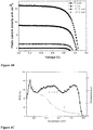
- 238000002190 incident photon conversion efficiency spectrum Methods 0.000 description 3
- RQQRAHKHDFPBMC-UHFFFAOYSA-L lead(ii) iodide Chemical compound I[Pb]I RQQRAHKHDFPBMC-UHFFFAOYSA-L 0.000 description 3
- 239000007791 liquid phase Substances 0.000 description 3
- 229910052759 nickel Inorganic materials 0.000 description 3
- ZKATWMILCYLAPD-UHFFFAOYSA-N niobium pentoxide Chemical compound O=[Nb](=O)O[Nb](=O)=O ZKATWMILCYLAPD-UHFFFAOYSA-N 0.000 description 3
- 229920000642 polymer Polymers 0.000 description 3
- 229910052718 tin Inorganic materials 0.000 description 3
- XLYOFNOQVPJJNP-UHFFFAOYSA-N water Substances O XLYOFNOQVPJJNP-UHFFFAOYSA-N 0.000 description 3
- 229910052724 xenon Inorganic materials 0.000 description 3
- FHNFHKCVQCLJFQ-UHFFFAOYSA-N xenon atom Chemical compound [Xe] FHNFHKCVQCLJFQ-UHFFFAOYSA-N 0.000 description 3
- 125000003184 C60 fullerene group Chemical group 0.000 description 2
- LFQSCWFLJHTTHZ-UHFFFAOYSA-N Ethanol Chemical compound CCO LFQSCWFLJHTTHZ-UHFFFAOYSA-N 0.000 description 2
- 229910018965 MCl2 Inorganic materials 0.000 description 2
- BAVYZALUXZFZLV-UHFFFAOYSA-N Methylamine Chemical compound NC BAVYZALUXZFZLV-UHFFFAOYSA-N 0.000 description 2
- 229910002370 SrTiO3 Inorganic materials 0.000 description 2
- 238000002835 absorbance Methods 0.000 description 2
- HSFWRNGVRCDJHI-UHFFFAOYSA-N alpha-acetylene Natural products C#C HSFWRNGVRCDJHI-UHFFFAOYSA-N 0.000 description 2
- PNEYBMLMFCGWSK-UHFFFAOYSA-N aluminium oxide Inorganic materials [O-2].[O-2].[O-2].[Al+3].[Al+3] PNEYBMLMFCGWSK-UHFFFAOYSA-N 0.000 description 2
- 125000004429 atom Chemical group 0.000 description 2
- 238000000231 atomic layer deposition Methods 0.000 description 2
- 229910052799 carbon Inorganic materials 0.000 description 2
- 150000001721 carbon Chemical group 0.000 description 2
- 229910052593 corundum Inorganic materials 0.000 description 2
- 239000003792 electrolyte Substances 0.000 description 2
- 238000005516 engineering process Methods 0.000 description 2
- 239000000284 extract Substances 0.000 description 2
- 229910052737 gold Inorganic materials 0.000 description 2
- 150000004820 halides Chemical class 0.000 description 2
- 238000011065 in-situ storage Methods 0.000 description 2
- 229910052741 iridium Inorganic materials 0.000 description 2
- 239000011244 liquid electrolyte Substances 0.000 description 2
- 230000033001 locomotion Effects 0.000 description 2
- 238000005259 measurement Methods 0.000 description 2
- 229910001507 metal halide Inorganic materials 0.000 description 2
- 150000005309 metal halides Chemical group 0.000 description 2
- 150000002739 metals Chemical class 0.000 description 2
- 125000002524 organometallic group Chemical group 0.000 description 2
- 229910052763 palladium Inorganic materials 0.000 description 2
- 229910052697 platinum Inorganic materials 0.000 description 2
- 229920001197 polyacetylene Polymers 0.000 description 2
- 229920000767 polyaniline Polymers 0.000 description 2
- 229920000128 polypyrrole Polymers 0.000 description 2
- 229920000123 polythiophene Polymers 0.000 description 2
- 230000005855 radiation Effects 0.000 description 2
- 229910052703 rhodium Inorganic materials 0.000 description 2
- 229910052707 ruthenium Inorganic materials 0.000 description 2
- 229910052709 silver Inorganic materials 0.000 description 2
- 239000007790 solid phase Substances 0.000 description 2
- 239000000126 substance Substances 0.000 description 2
- 229910052719 titanium Inorganic materials 0.000 description 2
- 239000010936 titanium Substances 0.000 description 2
- ZNOKGRXACCSDPY-UHFFFAOYSA-N tungsten(VI) oxide Inorganic materials O=[W](=O)=O ZNOKGRXACCSDPY-UHFFFAOYSA-N 0.000 description 2
- 229910001845 yogo sapphire Inorganic materials 0.000 description 2
- 125000000008 (C1-C10) alkyl group Chemical group 0.000 description 1
- STTGYIUESPWXOW-UHFFFAOYSA-N 2,9-dimethyl-4,7-diphenyl-1,10-phenanthroline Chemical compound C=12C=CC3=C(C=4C=CC=CC=4)C=C(C)N=C3C2=NC(C)=CC=1C1=CC=CC=C1 STTGYIUESPWXOW-UHFFFAOYSA-N 0.000 description 1
- GEQBRULPNIVQPP-UHFFFAOYSA-N 2-[3,5-bis(1-phenylbenzimidazol-2-yl)phenyl]-1-phenylbenzimidazole Chemical compound C1=CC=CC=C1N1C2=CC=CC=C2N=C1C1=CC(C=2N(C3=CC=CC=C3N=2)C=2C=CC=CC=2)=CC(C=2N(C3=CC=CC=C3N=2)C=2C=CC=CC=2)=C1 GEQBRULPNIVQPP-UHFFFAOYSA-N 0.000 description 1
- DIOURSRLPLXSNY-UHFFFAOYSA-N 2-[3,5-bis(4-phenyl-1h-benzimidazol-2-yl)phenyl]-4-phenyl-1h-benzimidazole Chemical compound C1=CC=CC=C1C1=CC=CC2=C1NC(C=1C=C(C=C(C=1)C=1NC3=C(C=4C=CC=CC=4)C=CC=C3N=1)C=1NC3=C(C=4C=CC=CC=4)C=CC=C3N=1)=N2 DIOURSRLPLXSNY-UHFFFAOYSA-N 0.000 description 1
- YEJRWHAVMIAJKC-UHFFFAOYSA-N 4-Butyrolactone Chemical compound O=C1CCCO1 YEJRWHAVMIAJKC-UHFFFAOYSA-N 0.000 description 1
- 125000000882 C2-C6 alkenyl group Chemical group 0.000 description 1
- 229910004613 CdTe Inorganic materials 0.000 description 1
- 239000004593 Epoxy Substances 0.000 description 1
- 229910005540 GaP Inorganic materials 0.000 description 1
- 229910001218 Gallium arsenide Inorganic materials 0.000 description 1
- 239000004793 Polystyrene Substances 0.000 description 1
- ATJFFYVFTNAWJD-UHFFFAOYSA-N Tin Chemical compound [Sn] ATJFFYVFTNAWJD-UHFFFAOYSA-N 0.000 description 1
- 238000002679 ablation Methods 0.000 description 1
- 238000011481 absorbance measurement Methods 0.000 description 1
- 238000010521 absorption reaction Methods 0.000 description 1
- 238000000862 absorption spectrum Methods 0.000 description 1
- 239000011149 active material Substances 0.000 description 1
- 239000000654 additive Substances 0.000 description 1
- 229910052782 aluminium Inorganic materials 0.000 description 1
- 229910052980 cadmium sulfide Inorganic materials 0.000 description 1
- UHYPYGJEEGLRJD-UHFFFAOYSA-N cadmium(2+);selenium(2-) Chemical compound [Se-2].[Cd+2] UHYPYGJEEGLRJD-UHFFFAOYSA-N 0.000 description 1
- 229910052792 caesium Inorganic materials 0.000 description 1
- AOWKSNWVBZGMTJ-UHFFFAOYSA-N calcium titanate Chemical compound [Ca+2].[O-][Ti]([O-])=O AOWKSNWVBZGMTJ-UHFFFAOYSA-N 0.000 description 1
- 239000002041 carbon nanotube Substances 0.000 description 1
- 229910021393 carbon nanotube Inorganic materials 0.000 description 1
- 239000002800 charge carrier Substances 0.000 description 1
- 229910052804 chromium Inorganic materials 0.000 description 1
- 239000002131 composite material Substances 0.000 description 1
- 230000007797 corrosion Effects 0.000 description 1
- 238000005260 corrosion Methods 0.000 description 1
- 230000008878 coupling Effects 0.000 description 1
- 238000010168 coupling process Methods 0.000 description 1
- 238000005859 coupling reaction Methods 0.000 description 1
- 238000004132 cross linking Methods 0.000 description 1
- 230000001419 dependent effect Effects 0.000 description 1
- 238000013461 design Methods 0.000 description 1
- 238000009792 diffusion process Methods 0.000 description 1
- 238000007598 dipping method Methods 0.000 description 1
- 238000010494 dissociation reaction Methods 0.000 description 1
- 230000005593 dissociations Effects 0.000 description 1
- 238000004090 dissolution Methods 0.000 description 1
- 239000002019 doping agent Substances 0.000 description 1
- 230000005670 electromagnetic radiation Effects 0.000 description 1
- 238000000295 emission spectrum Methods 0.000 description 1
- 230000005284 excitation Effects 0.000 description 1
- 230000001747 exhibiting effect Effects 0.000 description 1
- 230000002349 favourable effect Effects 0.000 description 1
- 230000004907 flux Effects 0.000 description 1
- 239000003574 free electron Substances 0.000 description 1
- 229910052949 galena Inorganic materials 0.000 description 1
- 238000003306 harvesting Methods 0.000 description 1
- 125000004051 hexyl group Chemical group [H]C([H])([H])C([H])([H])C([H])([H])C([H])([H])C([H])([H])C([H])([H])* 0.000 description 1
- XMBWDFGMSWQBCA-UHFFFAOYSA-N hydrogen iodide Chemical compound I XMBWDFGMSWQBCA-UHFFFAOYSA-N 0.000 description 1
- 229940071870 hydroiodic acid Drugs 0.000 description 1
- 230000006872 improvement Effects 0.000 description 1
- 238000002347 injection Methods 0.000 description 1
- 239000007924 injection Substances 0.000 description 1
- 229910010272 inorganic material Inorganic materials 0.000 description 1
- 239000011147 inorganic material Substances 0.000 description 1
- 229910052500 inorganic mineral Inorganic materials 0.000 description 1
- 239000001023 inorganic pigment Substances 0.000 description 1
- 239000011810 insulating material Substances 0.000 description 1
- 230000003993 interaction Effects 0.000 description 1
- 150000008040 ionic compounds Chemical class 0.000 description 1
- 229910052742 iron Inorganic materials 0.000 description 1
- JEIPFZHSYJVQDO-UHFFFAOYSA-N iron(III) oxide Inorganic materials O=[Fe]O[Fe]=O JEIPFZHSYJVQDO-UHFFFAOYSA-N 0.000 description 1
- 230000007774 longterm Effects 0.000 description 1
- 229910052749 magnesium Inorganic materials 0.000 description 1
- 229910052748 manganese Inorganic materials 0.000 description 1
- 125000002496 methyl group Chemical group [H]C([H])([H])* 0.000 description 1
- LLWRXQXPJMPHLR-UHFFFAOYSA-N methylazanium;iodide Chemical compound [I-].[NH3+]C LLWRXQXPJMPHLR-UHFFFAOYSA-N 0.000 description 1
- 239000011707 mineral Substances 0.000 description 1
- 238000002156 mixing Methods 0.000 description 1
- 239000002105 nanoparticle Substances 0.000 description 1
- 229910052758 niobium Inorganic materials 0.000 description 1
- QJGQUHMNIGDVPM-UHFFFAOYSA-N nitrogen group Chemical group [N] QJGQUHMNIGDVPM-UHFFFAOYSA-N 0.000 description 1
- 125000002347 octyl group Chemical group [H]C([*])([H])C([H])([H])C([H])([H])C([H])([H])C([H])([H])C([H])([H])C([H])([H])C([H])([H])[H] 0.000 description 1
- 230000005693 optoelectronics Effects 0.000 description 1
- 239000012044 organic layer Substances 0.000 description 1
- 239000011368 organic material Substances 0.000 description 1
- 238000013086 organic photovoltaic Methods 0.000 description 1
- 239000012860 organic pigment Substances 0.000 description 1
- 229910052762 osmium Inorganic materials 0.000 description 1
- 238000013082 photovoltaic technology Methods 0.000 description 1
- 229920000172 poly(styrenesulfonic acid) Polymers 0.000 description 1
- 239000002244 precipitate Substances 0.000 description 1
- 239000000047 product Substances 0.000 description 1
- 239000010453 quartz Substances 0.000 description 1
- 230000006798 recombination Effects 0.000 description 1
- 238000005215 recombination Methods 0.000 description 1
- 238000011160 research Methods 0.000 description 1
- 239000000565 sealant Substances 0.000 description 1
- 238000001338 self-assembly Methods 0.000 description 1
- 238000000926 separation method Methods 0.000 description 1
- 229910052710 silicon Inorganic materials 0.000 description 1
- VYPSYNLAJGMNEJ-UHFFFAOYSA-N silicon dioxide Inorganic materials O=[Si]=O VYPSYNLAJGMNEJ-UHFFFAOYSA-N 0.000 description 1
- 230000003381 solubilizing effect Effects 0.000 description 1
- 238000010129 solution processing Methods 0.000 description 1
- 229910052950 sphalerite Inorganic materials 0.000 description 1
- 238000003756 stirring Methods 0.000 description 1
- 238000006467 substitution reaction Methods 0.000 description 1
- 239000012780 transparent material Substances 0.000 description 1
- 229910052721 tungsten Inorganic materials 0.000 description 1
- 238000002061 vacuum sublimation Methods 0.000 description 1
- 239000012808 vapor phase Substances 0.000 description 1
- 238000001429 visible spectrum Methods 0.000 description 1
- 229910052725 zinc Inorganic materials 0.000 description 1
- 239000011701 zinc Substances 0.000 description 1
- 229910052984 zinc sulfide Inorganic materials 0.000 description 1
- 229910052726 zirconium Inorganic materials 0.000 description 1
Images

Classifications
-
- H—ELECTRICITY
- H10—SEMICONDUCTOR DEVICES; ELECTRIC SOLID-STATE DEVICES NOT OTHERWISE PROVIDED FOR
- H10K—ORGANIC ELECTRIC SOLID-STATE DEVICES
- H10K30/00—Organic devices sensitive to infrared radiation, light, electromagnetic radiation of shorter wavelength or corpuscular radiation
- H10K30/10—Organic devices sensitive to infrared radiation, light, electromagnetic radiation of shorter wavelength or corpuscular radiation comprising heterojunctions between organic semiconductors and inorganic semiconductors
-
- H—ELECTRICITY
- H10—SEMICONDUCTOR DEVICES; ELECTRIC SOLID-STATE DEVICES NOT OTHERWISE PROVIDED FOR
- H10K—ORGANIC ELECTRIC SOLID-STATE DEVICES
- H10K30/00—Organic devices sensitive to infrared radiation, light, electromagnetic radiation of shorter wavelength or corpuscular radiation
- H10K30/20—Organic devices sensitive to infrared radiation, light, electromagnetic radiation of shorter wavelength or corpuscular radiation comprising organic-organic junctions, e.g. donor-acceptor junctions
- H10K30/211—Organic devices sensitive to infrared radiation, light, electromagnetic radiation of shorter wavelength or corpuscular radiation comprising organic-organic junctions, e.g. donor-acceptor junctions comprising multiple junctions, e.g. double heterojunctions
-
- H—ELECTRICITY
- H10—SEMICONDUCTOR DEVICES; ELECTRIC SOLID-STATE DEVICES NOT OTHERWISE PROVIDED FOR
- H10K—ORGANIC ELECTRIC SOLID-STATE DEVICES
- H10K30/00—Organic devices sensitive to infrared radiation, light, electromagnetic radiation of shorter wavelength or corpuscular radiation
- H10K30/40—Organic devices sensitive to infrared radiation, light, electromagnetic radiation of shorter wavelength or corpuscular radiation comprising a p-i-n structure, e.g. having a perovskite absorber between p-type and n-type charge transport layers
-
- H—ELECTRICITY
- H10—SEMICONDUCTOR DEVICES; ELECTRIC SOLID-STATE DEVICES NOT OTHERWISE PROVIDED FOR
- H10K—ORGANIC ELECTRIC SOLID-STATE DEVICES
- H10K30/00—Organic devices sensitive to infrared radiation, light, electromagnetic radiation of shorter wavelength or corpuscular radiation
- H10K30/80—Constructional details
- H10K30/81—Electrodes
- H10K30/82—Transparent electrodes, e.g. indium tin oxide [ITO] electrodes
-
- H—ELECTRICITY
- H10—SEMICONDUCTOR DEVICES; ELECTRIC SOLID-STATE DEVICES NOT OTHERWISE PROVIDED FOR
- H10K—ORGANIC ELECTRIC SOLID-STATE DEVICES
- H10K85/00—Organic materials used in the body or electrodes of devices covered by this subclass
- H10K85/50—Organic perovskites; Hybrid organic-inorganic perovskites [HOIP], e.g. CH3NH3PbI3
-
- H—ELECTRICITY
- H10—SEMICONDUCTOR DEVICES; ELECTRIC SOLID-STATE DEVICES NOT OTHERWISE PROVIDED FOR
- H10K—ORGANIC ELECTRIC SOLID-STATE DEVICES
- H10K30/00—Organic devices sensitive to infrared radiation, light, electromagnetic radiation of shorter wavelength or corpuscular radiation
- H10K30/50—Photovoltaic [PV] devices
-
- H—ELECTRICITY
- H10—SEMICONDUCTOR DEVICES; ELECTRIC SOLID-STATE DEVICES NOT OTHERWISE PROVIDED FOR
- H10K—ORGANIC ELECTRIC SOLID-STATE DEVICES
- H10K30/00—Organic devices sensitive to infrared radiation, light, electromagnetic radiation of shorter wavelength or corpuscular radiation
- H10K30/80—Constructional details
- H10K30/87—Light-trapping means
-
- H—ELECTRICITY
- H10—SEMICONDUCTOR DEVICES; ELECTRIC SOLID-STATE DEVICES NOT OTHERWISE PROVIDED FOR
- H10K—ORGANIC ELECTRIC SOLID-STATE DEVICES
- H10K85/00—Organic materials used in the body or electrodes of devices covered by this subclass
- H10K85/10—Organic polymers or oligomers
- H10K85/111—Organic polymers or oligomers comprising aromatic, heteroaromatic, or aryl chains, e.g. polyaniline, polyphenylene or polyphenylene vinylene
- H10K85/113—Heteroaromatic compounds comprising sulfur or selene, e.g. polythiophene
- H10K85/1135—Polyethylene dioxythiophene [PEDOT]; Derivatives thereof
-
- H—ELECTRICITY
- H10—SEMICONDUCTOR DEVICES; ELECTRIC SOLID-STATE DEVICES NOT OTHERWISE PROVIDED FOR
- H10K—ORGANIC ELECTRIC SOLID-STATE DEVICES
- H10K85/00—Organic materials used in the body or electrodes of devices covered by this subclass
- H10K85/10—Organic polymers or oligomers
- H10K85/151—Copolymers
-
- H—ELECTRICITY
- H10—SEMICONDUCTOR DEVICES; ELECTRIC SOLID-STATE DEVICES NOT OTHERWISE PROVIDED FOR
- H10K—ORGANIC ELECTRIC SOLID-STATE DEVICES
- H10K85/00—Organic materials used in the body or electrodes of devices covered by this subclass
- H10K85/20—Carbon compounds, e.g. carbon nanotubes or fullerenes
- H10K85/211—Fullerenes, e.g. C60
- H10K85/215—Fullerenes, e.g. C60 comprising substituents, e.g. PCBM
-
- H—ELECTRICITY
- H10—SEMICONDUCTOR DEVICES; ELECTRIC SOLID-STATE DEVICES NOT OTHERWISE PROVIDED FOR
- H10K—ORGANIC ELECTRIC SOLID-STATE DEVICES
- H10K85/00—Organic materials used in the body or electrodes of devices covered by this subclass
- H10K85/30—Coordination compounds
-
- Y—GENERAL TAGGING OF NEW TECHNOLOGICAL DEVELOPMENTS; GENERAL TAGGING OF CROSS-SECTIONAL TECHNOLOGIES SPANNING OVER SEVERAL SECTIONS OF THE IPC; TECHNICAL SUBJECTS COVERED BY FORMER USPC CROSS-REFERENCE ART COLLECTIONS [XRACs] AND DIGESTS
- Y02—TECHNOLOGIES OR APPLICATIONS FOR MITIGATION OR ADAPTATION AGAINST CLIMATE CHANGE
- Y02E—REDUCTION OF GREENHOUSE GAS [GHG] EMISSIONS, RELATED TO ENERGY GENERATION, TRANSMISSION OR DISTRIBUTION
- Y02E10/00—Energy generation through renewable energy sources
- Y02E10/50—Photovoltaic [PV] energy
- Y02E10/549—Organic PV cells
Definitions
- the present invention relates to inverted organic-inorganic perovskite solar cells and methods for producing the same.
- PV photovoltaics
- the sandwich/monolithic-type PV devices consisting of a mesoporous photoanode with an organic/inorganic light harvester, redox electrolyte/solid-state hole conductor, and counter electrode, have gained significant interest due to the ease of fabrication, flexibility in the selection of materials and cost effective production ( Grätzel, M. Acc. Chem. Res. 2009, 42, 1788-1798 ).
- organometallic halide perovskite based on tin (CsSnX 3 ) or lead (CH 3 NH 3 PbX 3 ) Etgar, L.
- a common solvent i.e. N,N-dimethylformamide (DMF) or y-butyrolactone (GBL).
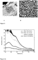
- the annealing process results in a crystalline CH 3 NH 3 PbX 3 (Noh et al cited above). From experience, the morphology of the perovskite crystals formed during this kind of solution processing cannot be well controlled and is one of the reasons for the poor reproducibility of PV cell performance.
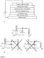
- solid-state solar cells or devices involve a conventional device architecture, in which the charge flow, namely the electrons and holes flow, is the following: a photoanode, mesoporous photoanode or current collector, collects the electrons. Holes are collected by a counter collector and/or metal layer.
- WO 2011/141706 A2 describes inverted and conventional device architectures.
- the anode comprising a hole collecting layer is on the top of the device stack and the electron collecting layer may be deposited on the transparent conductor.
- the hole collecting layer may be deposited onto the transparent conductor and the cathode comprising the electron collecting layer is on the top of the stack.
- These devices further comprise a photoactive layer as active layer comprising an organic dye. Modifying the surface of the adjacent layers to the photoactive layer by dipping their surface into the organic dye solution increases the current density in a device with an inverted architecture.
- US 2011/0079273 A1 also describes a kind of inverted photovoltaic device architectures comprising an organic sensitizer, in which the presence of a cascade layers reduces the recombination of the charges (holes and electron) and increases the efficiency.
- Lee et al. discloses solid state solar cells comprising an organic-inorganic perovskite as sensitizer, instead of an organic dye, on a mesostructured insulating scaffold from TiO 2 or Al 2 O 3 . These solar cells are solution processable and the organic-inorganic perovskite is spin-coated.
- US 6,117,498 describes a method for forming a film of organic-inorganic hybrid material, in particular organic-inorganic perovskite, said method being based on single source thermal ablation (SSTA) technique.
- SSTA single source thermal ablation
- the present invention addresses the disadvantage of the conventional architecture of solid state photovoltaic device regarding the air-stability of the top electrode (metal layer) of such a device, the poor long-term stability and life-time of the dcvicc, the cfficicncy and conductivity (separation of the charges) of such a device.
- the conventional architecture provides a limited number of possibilities to configure such devices to be optimized.
- the invention addresses the problems of corrosion and air-stability of the counter electrode and/or metal layer and of the contact between different organic layers to generate better ohmic contact and photon harvesting in order to improve the conductivity without providing heterostructure to facilitate efficient charge carrier generation. Inverting the charges flow in such a device is an efficient way to improve the efficiency as well as stability in PV device and in particular in solid state solar cell.
- the invention also addresses the use of organic-inorganic perovskite, which does not need to be in solution for their application or deposition to form a layer and to avoid the use of solvents, the step of annealing in the fabrication of the PV cells and the dissolution of the underneath layer of the perovskite layer during the application of this latter.
- the invention pursues to provide an efficient solar cell, which can be rapidly prepared in an efficient way, using readily available or low cost materials such as conductive material or hole transporting material, for example, using a short manufacturing procedure based on industrially known manufacturing step, using low temperatures manufacturing process, and using thin layer of electron and/or hole blocking material, keeping the material costs and the material impact on the environment very low.
- readily available or low cost materials such as conductive material or hole transporting material, for example, using a short manufacturing procedure based on industrially known manufacturing step, using low temperatures manufacturing process, and using thin layer of electron and/or hole blocking material, keeping the material costs and the material impact on the environment very low.
- the present invention addresses the problems depicted above.
- the present inventors have found that an organic-inorganic perovskite layer sandwiched between a thin electron blocking layer and/or hole transporting layer that blocks electrons and a thin hole blocking layer and/or electron transporting layer that blocks holes leads to very efficient solar cells.
- the present invention provides a method for producing a solid state solar cell with an inverted architecture and comprising an organic-inorganic perovskite film and/or organic-inorganic perovskite layer as the sensitizer layer according to claim 1.
- This method allows the application of the sensitizer layer having a thickness from 250 nm to 350 nm and consisting of organic-inorganic perovskite by co-deposition of sublimated components of the sensitizer perovskite components without heating the other layers of the partially assembled solar cell during the fabrication of said solar cell, keeping them at comparatively low-temperatures manufacturing process, which are compatible with the use of flexible substrates for the support layer of solar cell.
- Said method also allows the deposition of the different components of the sensitizer layer consisting of organic-inorganic perovskite in one step and without solubilizing the sensitizer layer consisting of organic-inorganic perovskite allowing the time- and cost-saving production of a sensitizer layer comprising organic-inorganic perovskite in situ without previously mixing the different components for obtaining the sensitizer layer consisting of organic-inorganic perovskite before its application, without using any solvent to liquefy the components before applying the sensitizer layer consisting of organic-inorganic perovskite.
- the present invention provides a solid state solar cell having an inverted architecture with an organic -inorganic perovskite layer of a thickness from 250 nm to 350 nm applied on an electron blocking layer according to claim 6.
- Said solar cell having an inverted architecture further comprises a hole blocking layer applied onto the perovskite layer, this latter being sandwiched between an electron blocking layer and a hole blocking layer.
- the present invention thus provides a solid solar cell with, the hole collector being on the side of the transparent front contact (namely an inverted architecture with respect to dye sensitized solar cell) according to claim 6.
- the present invention concerns a new method for producing solid solar cells and solar cells having a non-conventional design and architecture.
- the invention also concerns new solid solar cells with an inverted architecture, namely having the transparent front on the side of the hole collector.
- the method for producing a solid state solar cell comprises the steps of providing a hole collector layer; applying a conductive layer onto the hole collector layer; applying an electron blocking layer onto the conductive layer; applying a sensitizer layer onto the electron blocking layer; and providing a current collector and/or a metal layer or a conductor layer. This latter layer is in electric contact with the sensitizer layer.
- the method for producing a solid state solar cell further comprises a step of applying a hole blocking layer onto the sensitizer layer.
- the current collector and/or the metal layer or the conductor layer is in electric contact with the hole blocking layer.
- the method of invention comprises the steps of providing a hole collector layer; applying a conductive layer onto the hole collector layer; applying an electron blocking layer onto the conductive layer; applying a sensitizer layer onto the electron blocking layer; applying a hole blocking layer onto the sensitizer layer and providing a current collector and/or a metal layer or a conductor layer onto the hole blocking layer.
- the expression “in electric contact with” means that electrons or holes can get from one layer to the other layer with which it is in electric contact, at least in one direction.
- layers through which electrons and/or holes are flowing are considered to be in electric contact.
- the expression “in electric contact with” does not necessarily mean, and preferably does not mean, that electrons and/or holes can freely move in any direction between the layers.
- the method of the invention provides a sensitizer layer having a thickness from 250 nm to 350 nm and consisting of an organic-inorganic perovskite.
- the sensitizer layer comprises a further pigment in addition to the organic-inorganic perovskite pigment, said further pigment selected from organic pigment, organometallic pigment or inorganic pigment.
- Organometallic sensitizers are disclosed, for example, in EP0613466 , EP0758337 , EP 0983282 , EP 1622178 , WO2006/038823 , WO2009/107100 , WO2010/055471 and WO2011/039715 .
- Exemplary organic dyes are those disclosed in WO2009/098643 , EP1990373 , WO2007/100033 for example.
- An organic dye was also used in European patent application no. EP11161954.0 . and in PCT/IB2011/054628 .
- Metal free organic sensitizers such as DPP based compounds are disclosed, for example, in PCT/IB2013/056648 and in European patent application no. EP12182817.2 .
- perovskite refers to the “perovskite structure” and not specifically to the perovskite material, CaTiO3.
- perovskite encompasses and preferably relates to any material that has the same type of crystal structure as calcium titanium oxide and of materials in which the bivalent cation is replaced by two separate monovalent cations.
- the perovskite structure has the general stoichiometry AMX 3 , where "A" and "M” are cations and "X" is an anion.
- the "A” and “M” cations can have a variety of charges and in the original Perovskite mineral (CaTiO 3 ), the A cation is divalent and the M cation is tetravalent.
- the perovskite formulae includes structures having three (3) or four (4) anions, which may be the same or different, and/or one or two (2) organic cations, and/or metal atoms carrying two or three positive charges, in accordance with the formulae presented elsewhere in this specification.
- Organic-inorganic perovskites are hybrid materials exhibiting combined properties of organic composites and inorganic crystalline.
- the inorganic component forms a framework bound by covalent and ionic interactions, which provide high carrier mobility.
- the organic component helps in the self-assembly process of those materials, it also enables the hybrid materials to be deposited by low-cost technique as other organic materials. Additional important property of the organic component is to tailor the electronic properties of the organic-inorganic material by reducing its dimensionality and the electronic coupling between the inorganic sheets.
- the method of the invention provides the step of applying the sensitizer layer being performed at a vacuum from 10 -2 to 10 -10 mbar, 10 -2 to 10 -7 mbar, preferably at 10 -6 mbar.
- the step of applying the sensitizer layer consisting of the organic-inorganic perovskite is performed by deposition by sublimation process, wherein the sensitizer layer comprising an organic-inorganic perovskite is obtained by co-deposition of one or more sublimated divalent metal salts or sublimated trivalent metal salts and of one or more sublimated organic ammonium salts.
- Said deposition may be defined as co-deposition or deposition by sublimation process.
- sublimation means that this is the transition from the solid phase of a material (crystal for example) to the gas phase of said material (or vapor phase) without passing through an intermediate liquid phase at very low pressure, such as high vacuum.
- sublimation temperature corresponds to the term “heat of sublimation” being the temperature at which the phase transition from solid to gas without passing through the liquid phase is performed at a defined pressure. Said temperature depends on the type of the material, substance as well as the pressure in which this phase transition is performed.
- the relative expression “sublimated” or “sublimed” qualifies or defines the material (e.g. crystal of chemical compounds, of salts, of halide salts, of metallic salts, of organic salts), which has undergone a phase transition from the solid phase to the gas phase without passing through an intermediate liquid phase.
- the step of applying the sensitizer layer comprises heating the one or more divalent or trivalent salts and the ammonium salts up to their respective sublimation temperature to obtain a vapor of each salt, depositing said vapors onto the preceding layer and forming the inorganic-organic perovskite.
- This step or the process of fabrication the device may be performed without heating said device.
- the preceding layer is the electron blocking layer and/or the hole transporting layer of the partially assembled solar cell.
- Said step of depositing may be performed in a one step process as described above or in a multiple-steps process, wherein each salt forming the organic-inorganic perovskite is sublimated separately and deposited separately in several steps onto the preceding layer for forming the organic-inorganic perovskite layer.
- said one or more divalent metal salts or said one or more trivalent metal salts, which are heated to their respective sublimation temperature, are selected from salts of formula MX 2 or of formula NX 3 , respectively, wherein: M is a divalent metal cation selected from the group consisting of Cu 2+ , Ni 2+ , Co 2+ , Fe 2+ , Mn 2+ , Cr 2+ , Pd 2+ , Cd 2+ , Ge 2+ , Sn 2+ , Pb 2+ , Eu 2+ , or Yb 2+ ; N is selected from the group of Bi3+ and Sb3+; any X is independently selected from Cl - , Br - , I - , NCS - , CN - , and NCO - .
- said metal salt is MX 2 .
- said metal salt is a metal halide.
- these are different metal halides.
- said organic ammonium is selected from AX and BX 2 , A being an organic, monovalent cation selected from primary, secondary, tertiary or quaternary organic ammonium compounds, including N-containing heterorings and ring systems, A having from 1 to 60 carbons and 1 to 20 heteroatoms; and B being an organic, bivalent cation selected from primary, secondary, tertiary or quaternary organic ammonium compounds having from 1 to 60 carbons and 2 to 20 heteroatoms and having two positively charged nitrogen atoms.
- said organic ammonium is selected from AX.
- the divalent metal salts are of formula MX 2 and the trivalent metal salts are of formula NX 3 ,
- M being a divalent metal cation selected from the group consisting of Cu 2+ , Ni 2+ , Co 2+ , Fe 2+ , Mn 2+ , Cr 2+ , Pd 2+ , Cd 2+ , Ge 2+ , Sn 2+ , Pb 2+ , Eu 2+ , or Yb 2+ , N being selected from the group of Bi 3+ and Sb 3+ , and, X being independently selected from Cl - , Br - , I - , NCS - , CN - , and NCO - ; and the organic ammonium salts being selected from AX, AA' X 2 , and BX 2 , A and A' being independently selected from organic, monovalent cations selected from primary, secondary, tertiary or quaternary organic ammonium compounds, including N-containing heterorings and
- the two different salts are sublimated and applied by co-deposition at the same time or in two-steps.
- the crystal may contain different metal salts, which have been recrystallized together or the deposition may be performed from different crystals from different divalent salts, being sublimated at different temperature according to their respective sublimation temperature.
- Said different metals salts preferably differ with respect to the anion.
- the method of the invention comprises the steps of applying the sensitizer layer by co-deposition of two or more sublimated divalent salts selected from MX i 2 MX ii 2 and MX iii 2 , wherein X i , X ii and X ii i (charge not shown) are each different anions selected from I - , Cl - , Br - , I - , NCS - , CN - , and NCO - , preferably from I - , Cl - , and Br - .
- a mixed perovskite is obtained if the sublimated metal salt, in the state of vapor, comprising MX i 2 and MX ii 2 , or MX i 2 , MX i i2 and MX iii 2 , for example, may be co-deposited and/or combined with a sublimated organic ammonium salt, namely in the state of vapor, in accordance with the invention, which may be selected, independently from any one of AX i , AX ii and AX iii , under high vacuum, namely from 10 -2 to 10 -10 mbar, 10 -2 to 10 -7 mbar, preferably at or at least at 10 -6 mbar.
- the organic ammonium salt is selected from salts comprising one of the anions contained in the sublimated metal salt, for example from AX i or AX ii .
- the method of the invention comprises the step of applying the sensitizer layer, wherein said step is performed by co-deposition of two sublimated divalent metal salts, one said salt being MI 2 and the further being selected from MCl 2 and MBr 2 and of the sublimated ammonium organic salt AX, X being I - and A defined as above or below.
- M is Pb and/or A is CH 3 NH 3 + .
- the method of the invention comprises the step of applying the sensitizer layer, wherein said step is performed by co-deposition of two sublimated divalent metal salts, one said salt being MCl 2 and the further being selected from MI 2 and MBr 2 and of the sublimated ammonium organic salt AX, X being I - and A defined as above or below.
- M is Pb and/or A is CH 3 NH 3 + .
- the co-deposition of the one or more sublimated organic ammonium salts with the one or more sublimated divalent or trivalent metal salts concerns the co-deposition of one single and/or one structurally defined organic ammonium salt.
- a mixture of different sublimated organic salts is co-deposited. This is preferably valid irrespective from whether a mixture of different sublimated metal salts or if a single type of sublimated metal salts was co-deposited in the method of the invention.
- the method of the invention comprises the step of applying the sensitizer layer, wherein said step is performed by co-deposition of sublimated M i X 2 with sublimated M ii X or sublimated M iii X 3 , and of one or more sublimated ammonium organic salts as defined herein.
- Mii and Miii represent monovalent or trivalent cations, which would constitute a doping with a monovalent or trivalent metal salt, respectively.
- n-type or p-type doped metal salts and eventually perovskites can be obtained.
- said two different metal salts may be applied, differing with respect to the metal, but having, for example, identical anions.
- metals carrying different charges are preferably applied, resulting in doped perovskite or doped perovskite pigments.
- the step of applying the sensitizer layer is performed by one or more methods selected from physical vapor deposition methods group and/or from chemical vapor deposition.
- the physical vapor deposition methods group consists of deposition by sublimation process, cathodic arc deposition, electron beam physical vapor deposition, thermal evaporation, evaporative deposition, pulse laser deposition, sputter deposition.
- the sensitizer layer comprising an organic-inorganic perovskite may be applied in a first step: under the form of a film of the one or more divalent or trivalent metal salt, which is applied and/or deposited by a deposition method selected from thermal evaporation, deposition by sputtering, atomic-layer-deposition (ALD), and in a second step, under the application or deposition by anyone of the method as described above of the organic ammonium salt, thereby forming in situ the organic-inorganic perovskite layer.
- the steps of said two-step deposition method may be performed in any order.
- the sensitizer being an organic-inorganic perovskite may be also applied in one-step process.
- the application or deposition of the hole blocking layer is performed by a deposition method from a solution selected from drop casting, spin-coating, dip-coating, curtain coating, spray-coating, and ink- jet printing, meniscus, preferably by meniscus coating.
- the solution to be applied may comprise one or more hole blocking materials or two or more solutions may be mixed and applied either in a one-step process or in a two or more sequential steps process to form a film onto the sensitizer layer comprising or consisting of the organic-inorganic sensitizer.
- the step of applying the hole blocking layer is performed by one or more of the method of deposition as defined above, preferably by one or more physical vapor deposition methods, by chemical vapor deposition, by sublimation or deposition of sublimated hole blocking material, by deposition method from a solution (as defined above), meniscus coating.
- the hole blocking material functions as electron transporting material and extracts electrons from the sensitizer layer by preventing the transport of the holes.
- the hole blocking material is any material having HOMO energy level lower than HOMO energy level of the sensitizer layer or the organic-inorganic perovskite.
- the hole blocking layer has a LUMO energy level close to the conduction band of the perovskite.
- the hole blocking layer comprises one or more hole blocking material being selected from [6,6]-phenyl-C 61 -butyric acid methyl ester (PCBM), 1,4,5,8,9,11-hexazatriphenylene-hexacarbonitrile (HAT-CN), (C 60 -I h )[5,6]fullerene (C60), (C70-D5h)[5,6]fullerene (C70), [6,6]-Phenyl C 71 butyric acid methyl ester (PC70BM), 2,9-dimethyl-4,7-diphenyl-1,10-phenanthroline (BCP), 1,3,5-tri(phenyl-2-benzimi-dazolyl)-benzene (TPBI), preferably PCBM, HAT-CN, C60, C70, PC70BM, and metal oxide.
- PCBM hole blocking material being selected from [6,6]-phenyl-C 61 -butyric acid methyl ester
- HAT-CN 1,4,5,8,
- the metal oxide is an oxide of a metal selected from a group of metal consisting of Ti, Sn, Cs, Fe, Zn, W, Nb, SrTi, Si, Ti, Al, Cr, Sn, Mg, Mn, Zr, Ni, and Cu.
- a thin hole blocking layer onto the organic-inorganic perovskite layer, which is sandwiched between a thin electron blocking layer and said thin hole blocking layer, surprisingly enhances the open-circuit potential of a device, an optoelectronic device, an electrochemical device or a solar cell having such heterojunction, namely a perovskite layer sandwiched between a thin electron blocking layer and a thin hole blocking layer.
- the hole blocking layer has a thickness being ⁇ 10 nm, ⁇ 20 nm, ⁇ 50 nm, preferably ⁇ 10 nm.
- the step of providing the current collector and/or the metal layer or the conductor layer is performed by a method selected from the physical vapor deposition methods group as defined above, preferably by thermal evaporation onto the sensitizer layer or onto the perovskite layer or onto the sensitizer layer comprising a perovskite layer.
- Said step may be performed under vacuum, at a pressure from 10 -2 to 10 -10 mbar, 10 -2 to 10 -7 mbar, preferably of 2 ⁇ 10 -6 mbar.
- the current collector comprises or is a metal layer deposited by thermal evaporation.
- the step of providing the current collector and/or the metal layer or the conductor layer is performed by a deposition method from a solution as defined above, namely being selected from drop casting, spin-coating, dip-coating, curtain coating, spray-coating, and ink- jet printing, meniscus coating.
- the current collector and/or a metal layer or the conductor layer has a thickness being ⁇ 30 nm, ⁇ 50 nm, ⁇ 70 nm, ⁇ 90 nm, or ⁇ 110 nm, preferably ⁇ 70 nm. Accordingly, the step of providing the current collector and/or a metal layer or the conductor layer lasts up to that said current collector and/or metal layer or conductor layer has reached the desired thickness defined above.
- the step of applying the conductive layer is performed by a deposition method from one or more solutions of one or more conductive materials, said method selected from drop casting, spin-coating, dip-coating, curtain coating, spray-coating, and inkjet printing, preferably by spin-coating.
- the solution may comprise one or more conductive materials or two or more solutions may be mixed and applied in a one-step process to form a film onto the hole collector or applied in a process comprising two or more sequential steps.
- the step of applying the conductive layer is performed by a method selected from physical vapor deposition method group and/or from chemical vapor deposition as defined herein.
- the conductive material is selected from one or more conductive polymers or one or more hole transporting materials, which may be selected from poly(3,4-ethylenedioxythiophene):poly(styrenesulfonate) (PEDOT:PSS), poly(3,4-ethylenedioxythiophene):poly(styrenesulfonate):grapheme nanocomposite (PEDOT:PSS:graphene), poly(N-vinylcarbazole) (PVK) and sulfonated poly(diphenylamine) (SPDPA), preferably from PEDOT:PSS, PEDOT:PSS:graphene and PVK, more preferably from PEDOT:PSS.
- PEDOT:PSS poly(3,4-ethylenedioxythiophene):poly(styrenesulfonate)
- PVK poly(N-vinylcarbazole)
- SPDPA sulfonated poly(diphenylamine)
- Conductive polymers may also be selected from polymers comprising polyaniline, polypyrrole, polythiophene, polybenzene, polyethylenedioxythiophene, polypropylenedioxy-thiophene, polyacetylene, and combinations of two or more of the aforementioned, for example.
- the conductive polymer of the invention is preferably selected from the above polymer in a watery dispersion.
- hole transport material By “hole transport material”, “hole transporting material”, “charge transporting material”, “organic hole transport material” and “inorganic hole transport material”, and the like, is meant any material or composition wherein charges are transported by electron or hole movement (electronic motion) across said material or composition.
- the “hole transport material” is thus an electrically conductive material.
- Such hole transport materials, etc. are different from electrolytes. In this latter, charges are transported by diffusion of molecules.
- the conductive material functions as a hole transporting material and as a hole injection material to bring holes extracted from the sensitizer layer to the hole collector of the solid solar cell, in particular of the inverted solid solar cell of the invention, wherein the hole collector is on the side of the transparent electrode or front contact. Accordingly, said conductive material enhances the extraction of holes.
- the conductive material layer allows to smooth and to uniform the nanoporous semiconductor being the hole collector.
- the step of applying the conductive layer is performed by spin-coating a solution of a conductive polymer selected from poly(3,4-ethylenedioxythiophene):poly(styrenesulfonate) (PEDOT:PSS), poly(3,4-ethylenedioxythiophene):poly(styrenesulfonate):grapheme nanocomposite (PEDOT:PSS:graphene), poly(N-vinylcarbazole) (PVK) and sulfonated poly(diphenylamine) (SPDPA), preferably from PEDOT:PSS, PEDOT:PSS:graphene and PVK, more preferably from PEDOT:PSS.
- a conductive polymer selected from poly(3,4-ethylenedioxythiophene):poly(styrenesulfonate) (PEDOT:PSS), poly(3,4-ethylenedioxythiophene):poly(styrenesulfonate):graphe
- the conductive layer is applied and/or deposited by spin-coating a solution comprising one or more conductive materials or defined as conductive at 1'000 rpm or more, 1'200 rpm or more, 2'000 rpm or more, 3'000 rpm or more, preferably at 1'200 rpm or more.
- the spin-coating takes place for 1 s (second) to 10 minutes, preferably 2 s to 30 s.
- the conductive layer has a thickness being ⁇ 30 nm, ⁇ 50 nm, ⁇ 70 nm, ⁇ 90 nm, or ⁇ 110 nm, preferably ⁇ 70 nm. Accordingly, the step of applying the conductive layer lasts up to that said conductive layer has reached the desired thickness defined above.
- the application or deposition of the electron blocking layer is performed by a deposition method from solution selected from drop casting, spin-coating, dip-coating, curtain coating, spray-coating, and ink- jet printing, meniscus, preferably by meniscus coating.
- the solution may comprise one or more electron blocking material or two or more solutions may mixed and applied in a one-step process to form a film onto the hole collector or applied in a process comprising two or more sequential steps.
- the application or deposition of the electron blocking layer may be performed by a physical vapor deposition method, a chemical vapor deposition method or a deposition by sublimation, namely sublimation.
- the electron blocking material functions as hole transporting material and extracts holes from the sensitizer layer by preventing the transport of the electron.
- the electron blocking material is any material having LUMO energy level higher than the sensitizer layer or the organic-inorganic perovskite LUMO energy level.
- the HOMO energy level of an electron blocking layer is closed to the valence band of the perovskite.
- the electron blocking layer and/or hole transporting layer comprises an electron blocking material being selected from aromatic amine derivatives selected from triphenylamine, carbazole, N,N,(diphenyl)-N',N'di-(alkylphenyl)-4,4'-biphenyldiamine, (pTPDs), diphenylhydrazone, poly [N,N'-bis(4-butylphenyl)-N,N'-bis(phenyl)benzidine] (polyTPD), polyTPD substituted by electron donor groups and/or acceptor groups, poly(9,9-dioctylfluorene-alt-N-(4-butylphenyl)-diphenylamine (TFB), 2,2',7,7'-tetrakis-N,N-di-p-methoxyphenylamine-9,9'-spirobifluorene) (spiro-OMeTAD), N,
- the electron blocking layer has a thickness being ⁇ 5, ⁇ 10 nm, ⁇ 20 nm, ⁇ 50 nm, preferably from 4 to 50 nm, from 5 to 20 nm.
- organic in expressions "organic hole transport material”, “organic hole transport layer”, “organic charge transport material” “electron blocking layer” and the like does not exclude the presence of further components.
- Further components may be selected from (a) one or more dopants, (b) one or more solvents, (c) one or more other additives such as ionic compounds, and (c) combinations of the aforementioned components, for example.
- such further components may be present in amounts of 0-30wt.%, 0-20wt.%, 0-10wt.%, most preferably 0-5wt.%.
- the step of providing a hole collector layer comprises a step of providing a conducting layer being transparent and a step of applying a conducting material onto the conducting layer.
- the hole collector layer may comprise a conducting layer being transparent and a conducting material.
- Said conducting layer is selected from conducting glass or conducting plastic.
- the conducting material is selected from indium doped thin oxide (ITO), fluorine doped tin oxide (FTO), ZnO-Ga 2 O 3 , ZnO-Al 2 O 3 , tin-oxide, antimony doped tin oxide (ATO), SrGeO 3 and zinc oxide.
- the hole collector may comprise or may consist of a conducting layer and a conductive material.
- the step of providing a hole collector layer comprises a further step of providing a surface-increasing scaffold structure between the conducting layer and the conducting material layer.
- the hole collector layer may comprise a conducting layer, a surface-increasing scaffold structure and a conducting material layer.
- the method of invention comprises a further step of providing a support layer on the external side of the hole collector.
- Said support layer may be the hole collector or the conducting layer of the hole collector, or comprises the hole collector or is provided before the conducting layer of the hole collector, namely to the external side of the hole collector.
- the method of invention comprises a further step of providing a support layer on the side of the current collector and/or metal layer or conductor layer, preferably on the top of the current collector and/or metal layer or conductor layer.
- the invention also provides a solid state solar cell obtainable by the method of the invention.
- the solid state solar cell comprising a hole collector layer under a conductive layer, an electron blocking layer, a sensitizer layer having a thickness of 150 nm to 350 nm and consisting of an organic-inorganic perovskite being coated by a hole blocking layer and a current collector layer, wherein the hole collector layer is coated by the conductive layer; wherein the electron blocking layer is between the conductive layer and the sensitizer layer, which is in contact with the current collector layer being a metal or a conductor.
- the invention also provides, the invention provides a solid state solar cell comprising a hole collector layer, a conductive polymer layer, an electron blocking layer, a sensitizer layer consisting of an organic-inorganic perovskite having a thickness from 250 nm to 350 nm, a hole blocking layer and a current collector layer, wherein the hole collector layer is coated by the conductive polymer layer; wherein the electron blocking layer is between the conductive polymer layer and the perovskite layer coated by the hole blocking layer, which is in contact with the current collector layer being a metal or a conductor.
- the hole collector layer of the solid state solar cell is on the side exposed to the light.
- the hole collector is preferably arranged to collect and conduct the holes generated in the sensitizer layer. Therefore, the current collector is preferably in electric contact with the photocathode.
- the solar cell of the invention preferably comprises one or more support layers.
- the support layer preferably provides physical support of the device.
- the support layer preferably provides a protection with respect to physical damage and thus delimits the solar cell with respect to the outside, for example on at least one of the two sides of the solar cell, the one exposed to the light (support layer) or to the opposite side remaining in the dark (current support layer).
- the solar cell may be constructed by applying the different layers in a sequence of steps, one after the other, onto the support layer.
- the support layer may thus also serve as a starting support for the fabrication of the solar cell.
- Support layers may be provided on only one or on both opposing sides of the solar cell.
- the support layer if present, is preferably transparent, so as to let light pass through the solar cell.
- the support layer if the support layer is provided on the side of the solar cell that is not directly exposed to light to be converted to electrical energy, the support does not necessarily have to be transparent.
- any support layer provided on the side that is designed and/or adapted to be exposed to light for the purpose of energy conversion is preferably transparent.
- Transparent means transparent to at least a part, preferably a major part of the visible light.
- the support layer is substantially transparent to all wavelengths or types of visible light.
- the support layer may be transparent to non-visible light, such as UV and IR radiation, for example.
- a support layer is provided, said support layer serving as support as described above as well as the conducting layer of the hole collector.
- the support layer thus replaces or contains the conducting layer.
- the support layer is preferably transparent.
- support layers are conducting glass or conducting plastic, which are commercially available.
- the support layer comprises a material selected from indium doped tin oxide (ITO), fluorine doped tin oxide (FTO), ZnO-Ga 2 O 3 , ZnO-Al 2 O 3 , tin oxide, antimony doped tin oxide (ATO), SrGeO 3 and zinc oxide, coated on a transparent substrate, such as plastic or glass.
- the surface-increasing scaffold structure when a surface-increasing scaffold structure is provided between the conducting layer and the conducting material of the holes conductor, the surface-increasing scaffold structure is nanostructured and/or nanoporous.
- the scaffold structure is thus preferably structured on a nanoscale.
- the structures of said scaffold structure increase the effective surface compared to the surface of the conducting layer.
- the surface-increasing scaffold structure of the solar cell of the invention comprises, consists essentially of or is made from one selected from the group consisting of a semiconductor material, a conducting material, a non-conducting material and combinations of two or more of the aforementioned.
- said scaffold structure is made from and/or comprises a metal oxide.
- the material of the scaffold structure is selected from semiconducting materials, such as Si, TiO 2 , SnO 2 , Fe 2 O 3 , ZnO, WO 3 , Nb 2 O 5 , CdS, ZnS, PbS, Bi 2 S 3 , CdSe, CdTe, SrTiO 3 , GaP, InP, GaAs, CuInS 2 , CuInSe 2 , and combinations thereof, for example.
- Preferred semiconductor materials are Si, TiO 2 , SnO 2 , ZnO, WO 3 , Nb 2 O 5 and SrTiO 3 .
- the material of the scaffold structure does not need to be semiconducting or conducting, but could actually be made from a non-conducting and/or insulating material.
- the scaffold structure could be made from plastics, for example from plastic nanoparticles, which are in any way assembled on the support and are fixed thereon, for example by heating and/or cross-linking.
- Polystyrene (PS) spheres of sub-25 micrometer size deposited on a conducting substrate can be cited as an example of a non-conducting scaffold structure.
- the organic-inorganic perovskite material that is used and/or obtained in the one or more perovskite layer preferably comprises a perovskite-structure of any one of formulae (I), (II) , (III), (IV), (V) and/or (VI) below: AA'MX 4 (I) AMX 3 (II) AA'N 2/3 X 4 (III) AN 2/3 X 3 (IV) BN 2/3 X 4 (V) BMX 4 (VI) wherein,
- AMX 3 (formula II) may be expressed as formula (II') below: AMX i X ii X iii (II') wherein X i , X ii , X iii are independently selected from Cl - , Br - , I - , NCS - , CN - , and NCO - , preferably from halides (Cl - , Br - , I - ), and A and M are as defined elsewhere in this specification.
- X i , X ii , X iii may thus be the same or different in this case.
- formula (I') applies: AA'M X i X ii X iii X iv (I') wherein X i , X ii , X iii are independently selected from Cl - , Br - , I - , NCS - , CN - , and NCO - , preferably from halides (Cl - , Br - , I - ).
- X i , X ii , X iii in formulae (II) and (IV) or X i , X ii , X iii , X iv in formulae (I), (III), (V) or (VI) comprise different anions X, there are not more than two different anions.
- X i and X ii being the same with X iii being an anion that is different from X i and X ii .
- the perovskite material has the structure selected from one or more of formulae (I) to (III), preferably (II) or (II').
- said organic-inorganic perovskite layer comprises a perovskite-structure of any one of the formulae (VIII) to (XIV): APbX 3 (VIII) ASnX 3 (IX) ABiX 4 (X) AA'PbX 4 (XI) AA'SnX 4 (XII) BPbX 4 (XIII) BSnX 4 (XIV) wherein A, A', B and X are as defined elsewhere in this specification.
- X is preferably selected from Cl - , Br - and I - , most preferably X is I - .
- said organic-inorganic perovskite layer comprises a perovskite-structure of the formulae (VIII) to (XII), more preferably (VIII) and/or (IX) above.
- a and A' for example in AX and/or in any one of formulae (I) to (IV), and (VIII) to (XII), are monovalent cations selected independently from any one of the compounds of formulae (1) to (8) below: wherein, any one of R 1 , R 2 , R 3 and R 4 is independently selected from C1-C15 organic substituents comprising from 0 to 15 heteroatoms.
- any one, several or all hydrogens in said substituent may be replaced by halogen and said organic substituent may comprise up to fifteen (15) N, S or O heteroatoms, and wherein, in any one of the compounds (2) to (8), the two or more of substituents present (R 1 , R 2 , R 3 and R 4 , as applicable) may be covalently connected to each other to form a substituted or unsubstituted ring or ring system.
- any heteroatom is connected to at least one carbon atom.
- neighboring heteroatoms are absent and/or heteroatom-heteroatom bonds are absent in said C1-C15 organic substituent comprising from 0 to 15 heteroatoms.
- any one of R 1 , R 2 , R 3 and R 4 is independently selected from C1 to C15 aliphatic and C4 to C15 aromatic or heteroaromatic substituents, wherein any one, several or all hydrogens in said substituent may be replaced by halogen and wherein, in any one of the compounds (2) to (8), the two or more of the substituents present may be covalently connected to each other to form a substituted or unsubstituted ring or ring system.
- B is a bivalent cation selected from any one of the compounds of formulae (9) and (10) below: wherein,
- the number of heteroatoms is smaller than the number of carbons.
- the number of ring heteroatoms is smaller than the number of carbon atoms.
- L is an aliphatic, aromatic or heteroaromatic linker structure having from 1 to 10 carbons.
- the dotted line in substituents (20) to (25) represents a carbon-nitrogen bond, connecting the nitrogen atom shown in the substituent to a carbon atom of the linker.
- L is an organic linker structure having 1 to 8 carbons and from 0 to 4 N, S and/or O heteroatoms, wherein any one, several or all hydrogens in said L may be replaced by halogen.
- L is an aliphatic, aromatic or heteroaromatic linker structure having 1 to 8 carbons, wherein any one, several or all hydrogens in said L may be replaced by halogen.
- L is an organic linker structure having 1 to 6 carbons and from 0 to 3 N, S and/or O heteroatoms, wherein any one, several or all hydrogens in said L may be replaced by halogen.
- L is an aliphatic, aromatic or heteroaromatic linker structure having 1 to 6 carbons, wherein any one, several or all hydrogens in said L may be replaced by halogen.
- said linker L is free of any O or S heteroatoms. According to an embodiment, L is free of N, O and/or S heteroatoms.
- the circle containing said two positively charged nitrogen atoms represents a substituted or unsubstituted aromatic ring or ring system comprising 4 to 10 carbon atoms and 2 to 5 heteroatoms (including said two ring N-atoms).
- said ring or ring system in the compound of formula (10) is free of any O or S heteroatoms. According to an embodiment, said ring or ring system in the compound of formula (10) is free of any further N, O and/or S heteroatoms, besides said two N-ring atoms. This does not preclude the possibility of hydrogens being substituted by halogens.
- an aromatic linker, compound, substituent or ring comprises 4 carbons, it comprises at least 1 ring heteroatom, so as to provide an aromatic moiety.
- any one of R 1 , R 2 , R 3 and R 4 is independently selected from C1 to C8 organic substituents comprising, from 0 to 4 N, S and/or O heteroatom, wherein, independently of said N, S or O heteroatoms, any one, several or all hydrogens in said substituent may be replaced by halogen, and wherein two or more of substituents present on the same cation may be covalently connected to each other to form a substituted or unsubstituted ring or ring system.
- any one of R 1 , R 2 , R 3 and R 4 is independently selected from C1 to C8 aliphatic, C4 to C8 heteroaromatic and C6 to C8 aromatic substituents, wherein said heteroaromatic and aromatic substituents may be further substituted.
- any one of R 1 , R 2 , R 3 and R 4 is independently selected from C1 to C6 organic substituents comprising, from 0 to 3 N, S and/or O heteroatom, wherein, independently of said N, S or O heteroatoms, any one, several or all hydrogens in said substituent may be replaced by halogen, and wherein two or more of substituents present on the same cation may be covalently connected to each other to form a substituted or unsubstituted ring or ring system.
- any one of R 1 , R 2 , R 3 and R 4 is independently selected from C1 to C6 aliphatic, C4 to C6 heteroaromatic and C6 to C6 aromatic substituents, wherein said heteroaromatic and aromatic substituents may be further substituted.
- any one of R 1 , R 2 , R 3 and R 4 is independently selected from C1 to C4, preferably C1 to C3 and most preferably C1 to C2 aliphatic substituents wherein any one, several or all hydrogens in said substituent may be replaced by halogen and wherein two or more of substituents present on the same cation may be covalently connected to each other to form a substituted or unsubstituted ring or ring system.
- any one of R 1 , R 2 , R 3 and R 4 is independently selected from C1 to C10 alkyl, C2 to C10 alkenyl, C2 to C10 alkynyl, C4 to C10 heteroaryl and C6 to C10 aryl, wherein said alkyl, alkenyl, and alkynyl, if they comprise 3 or more carbons, may be linear, branched or cyclic, wherein said heteroaryl and aryl may be substituted or unsubstituted, and wherein several or all hydrogens in R 1 -R 4 may be replaced by halogen.
- any one of R 1 , R 2 , R 3 and R 4 is independently selected from C1 to C8 alkyl, C2 to C8 alkenyl, C2 to C8 alkynyl, C4 to C8 heteroaryl and C6 to C8 aryl, wherein said alkyl, alkenyl, and alkynyl, if they comprise 3 or more carbons, may be linear, branched or cyclic, wherein said heteroaryl and aryl may be substituted or unsubstituted, and wherein several or all hydrogens in R 1 -R 4 may be replaced by halogen.
- any one of R 1 , R 2 , R 3 and R 4 is independently selected from C1 to C6 alkyl, C2 to C6 alkenyl, C2 to C6 alkynyl, C4 to C6 heteroaryl and C6 aryl, wherein said alkyl, alkenyl, and alkynyl, if they comprise 3 or more carbons, may be linear, branched or cyclic, wherein said heteroaryl and aryl may be substituted or unsubstituted, and wherein several or all hydrogens in R 1 -R 4 may be replaced by halogen.
- any one of R 1 , R 2 , R 3 and R 4 is independently selected from C1 to C4 alkyl, C2 to C4 alkenyl and C2 to C4 alkynyl, wherein said alkyl, alkenyl and alkynyl, if they comprise 3 or more carbons, may be linear, branched or cyclic, and wherein several or all hydrogens in in R 1 -R 4 may be replaced by halogen.
- any one of R 1 , R 2 , R 3 and R 4 is independently selected from C1 to C3, preferably C1 to C2 alkyl, C2 to C3, preferably C2 alkenyl and C2 to C3, preferably C2 alkynyl, wherein said alkyl, alkenyl and alkynyl, if they comprise 3 or more carbons, may be linear, branched or cyclic, and wherein several or all hydrogens in R 1 -R 4 may be replaced by halogen.
- any one of R 1 , R 2 , R 3 and R 4 is independently selected from C1 to C4, more preferably C1 to C3 and even more preferably C1 to C2 alkyl. Most preferably, any one of R 1 , R 2 , R 3 and R 4 are methyl. Again, said alkyl may be completely or partially halogenated.
- A, A' and B are monovalent (A, A') and bivalent (B) cations, respectively, selected from substituted and unsubstituted C5 to C6 rings comprising one, two or more nitrogen heteroatoms, wherein one (for A and A') or two (for B) of said nitrogen atoms is/are positively charged.
- Substituents of such rings may be selected from halogen and from C1 to C4 alkyls, C2 to C4 alkenyls and C2 to C4 alkynyls as defined above, preferably from C1 to C3 alkyls, C3 alkenyls and C3 alkynyls as defined above.
- Said ring may comprise further heteroatoms, which may be selected from O, N and S.
- Bivalent organic cations B comprising two positively charged ring N-atoms are exemplified, for example, by the compound of formula (10) above.
- Such rings may be aromatic or aliphatic, for example.
- A, A' and B may also comprise a ring system comprising two or more rings, at least one of which being from substituted and unsubstituted C5 to C6 ring as defined as above.
- the elliptically drawn circle in the compound of formulae (10) may also represent a ring system comprising, for example, two or more rings, but preferably two rings. Also if A and/or A' comprises two rings, further ring heteroatoms may be present, which are preferably not charged, for example.
- the organic cations A, A' and B comprise one (for A, A'), two (for B) or more nitrogen atom(s) but are free of any O or S or any other heteroatom, with the exception of halogens, which may substitute one or more hydrogen atoms in cation A and/or B.
- a and A' preferably comprise one positively charged nitrogen atom.
- B preferably comprises two positively charged nitrogen atoms.
- A, A' and B may be selected from the exemplary rings or ring systems of formulae (30) and (31) (for A) and from (32) to (34) (for B) below: in which R 1 and R 2 are, independently, as defined above, and R 3 , R 4 , R 5 , R 6 , R 7 , R 8 , R 9 and R 10 are independently selected from H, halogen and substituents as defined above for R 1 to R 4 .
- R 3 -R 10 are selected from H and halogen, most preferably H.
- hydrogens may be substituted by halogens, such as F, Cl, I, and Br, preferably F or Cl.
- halogens such as F, Cl, I, and Br, preferably F or Cl.
- a and A' are independently selected from organic cations of formula (1).
- R 1 in the cation of formula (1) is selected from C1 to C8 organic substituents comprising, from 0 to 4 N, S and/or O heteroatom. More preferably, R 1 is selected from C1 to C4, preferably C1 to C3 and most preferably C1 to C2 aliphatic substituents.
- the metal M is selected from Sn 2+ and Pb 2+ , preferably Pb 2+ .
- N is Sb 3+ .
- the three or four X are independently selected from Cl - , Br - , and I - .
- the organic-inorganic perovskite material has the formula of formulae (XV) to (XIX) below: AMI 3 (XV) AMI 2 Br (XVI) AMI 2 Cl (XVII) AMBr 3 (XVII) AMCl 3 (XIX) wherein A and M are as defined elsewhere in this specification, including the preferred embodiments of A and M, such as those defined below.
- M is selected from Sn 2+ and Pb 2+ .
- A is selected from organic cations of formula (1).
- R 1 in the cation of formula (1) is selected from C1 to C8 organic substituents comprising, from 0 to 4 N, S and/or O heteroatom. More preferably, R 1 is selected from C1 to C4, preferably C1 to C3 and most preferably C1 to C2 aliphatic substituents.
- the organic-inorganic perovskite is a compound of formula (VII) (AMX i X ii X iii ), wherein A is a monovalent cation of formula (1) as defined above, M is as defined elsewhere in this specification, and X i , X ii , X iii are independently selected from Cl - , Br - , I - .
- R 1 in the cation of formula (1) is selected from C1 to C4, preferably C1 to C3 and most preferably C1 to C2 aliphatic substituents.
- the organic-inorganic perovskite is a compound of formula (VII) (AMX i X ii X iii ), wherein A is a monovalent cation of formula (1) as defined above, M is Sn 2+ or Pb 2+ , and X i , X ii , X iii are independently selected from Cl - , Br - , I - .
- R 1 in the cation of formula (1) is selected from C1 to C4, preferably C1 to C3 and most preferably C1 to C2 aliphatic substituents.
- X i ⁇ X iii are identical.
- the sensitizer layer having a thickness from 250 nm to 350 nm consists of an organic-inorganic perovskite layer.
- the current collector of the solar cell of the invention is on the dark side.
- the current collector is preferably arranged to collect and conduct the electron generated in the perovskite layer.
- the current collector faces the sensitizer layer towards the inside of the solar cell.
- the current collector is the outmost layer and thus the one of the outer surfaces of the cell. It is also possible that a support layer is present on one side of the current collector.
- the current collector comprises or consists of or is a metal or a conductor, which is in in direct contact with the preceding layer being the sensitizer layer or the hole blocking layer, if said hole blocking layer is present.
- the current collector comprises or consists of or is a conductor, which may be in direct contact with the sensitizer layer and/or not separated by any further layer or medium from said sensitizer layer.
- the current collector comprises a catalytically active material, suitable to provide electrons and/or fill holes towards the inside of the device.
- the current collector may comprise a metal or a conductor or may be a metal layer or a conductor layer.
- the current collector may comprise one or more materials being metals selected from Pt, Au, Ni, Cu, Ag, In, Ru, Pd, Rh, Ir, Os, C or conductors selected from carbon nanotubes, graphene and grapheme oxides, conductive polymer and a combination of two or more of the aforementioned.
- Conductive polymers may be selected from polymers comprising polyaniline, polypyrrole, polythiophene, polybenzene, polyethylenedioxythiophene, polypropylenedioxythiophene, polyacetylene, and combinations of two or more of the aforementioned.
- the current collector comprises a metal selected from Pt, Au, Ni, Cu, Ag, In, Ru, Pd, Rh, Ir, Os, preferably Au.
- the current collector may comprise a conductor being transparent material selected from indium doped tin oxide (ITO), fluorine doped tin oxide (FTO), ZnO-Ga 2 O 3 , ZnO-Al 2 O 3 , tin oxide, antimony doped tin oxide (ATO), SrGeO 3 and zinc oxide.
- ITO indium doped tin oxide
- FTO fluorine doped tin oxide
- ZnO-Ga 2 O 3 ZnO-Al 2 O 3
- tin oxide antimony doped tin oxide
- ATO antimony doped tin oxide
- SrGeO 3 zinc oxide
- the current collector is connected to the external circuit.
- a conductive support such as conductive glass or plastic may be electrically connected to the counter electrode on the second side.
- solar cell according to an embodiment of the invention exhibits a power conversion efficiency (PCE) of ⁇ 4%, preferably ⁇ 5%, more preferably ⁇ 6%, and most preferably ⁇ 7%, measured in standard air mass 1.5 global (AM1.5G) sunlight conditions, corresponding to a solar zenith angle of 48.2°, a solar light intensity of 100 mW cm 2 and a cell temperature of 25°C.
- PCE power conversion efficiency
- Example 1 Fabrication of a solid solar of the invention having a sensitizer sandwiched between an electron blocking layer and a hole blocking layer.
- Photolithographically patterned ITO covered glass substrates were purchased from NaranjoSubstrates.
- Aqueous dispersions of poly(3,4-ethylenedioxythiophene) doped with poly(styrenesulfonate) (PEDOT:PSS, CLEVIOS P VP Al 4083) were obtained from Heraeus Holding GmbH and used as received.
- poly[N,N'-bis(4-butylphenyl)-N,N'-bis(phenyl)benzidine] (poly-TPD) was purchased from ADS Dyesource.
- CH 3 NH 3 I was prepared similar to a previously published method, in brief: CH 3 NH 3 I, was synthesized by reacting 21.6 ml methylamine (40%wt in water, Aldrich) and 30 ml hydroiodic acid (57 wt% in water,Aldrich) in a 250 ml roundbottomed flask at 0°C for 2 h with stirring. The white precipitate was recovered by evaporation at 50°C for 1 h. The product, methylammonium iodide (CH 3 NH 3 I), was dissolved in ethanol, filtered and recrystallized from diethyl ether, and dried at 60°C in a vacuum oven for 24 h.
- CH 3 NH 3 I methylammonium iodide
- Devices were prepared on cleaned ITO substrates, by spin-coating a thin layer of PEDOT:PSS from the commercial aqueous dispersion (1200rpm 30sec result in 70 nm thickness).
- a thin film ( ⁇ 10 nm) of polyTPD functioning as the electron blocking layer was deposited from a chlorobenzene solution (10 mg.ml ⁇ 1 ) using a meniscus coater and a coating speed of 2.5 mm/s.
- the substrates were transferred to a vacuum chamber integrated into an inert glovebox (MBraun, ⁇ 0.1 ppm O 2 and ⁇ 0.1 ppm H 2 O) and evacuated to a pressure of 1 ⁇ 10 -6 mbar.
- the film thickness was controlled by the PbI 2 evaporation at a rate of evaporation of 0.5 Angstrom per second.
- the perovskite layer thickness is of 350 nm.
- the PCBM layer functioning as the hole blocking layer was deposited as a thin layer ( ⁇ 10nm) using a chlorobenzene solution of 10 mg.ml ⁇ 1 in ambient conditions using a meniscus coater and a coating speed of 2.5 mm/s.
- the device was completed by the thermal evaporation of the top metal (Au) electrode under a base pressure of 2 ⁇ 10 -6 mbar to a thickness of 100 nm.
- the solar cells active area of 0.09 and 0.98 mm 2 ) were than encapsulated with a glass cover using a UV curable epoxy sealant.
- IPCE Incident photon-to-current conversion efficiency
- the roughness of the CH 3 NH 3 PbI 3 film was evaluated using Atomic Force Microscopy (AFM) and an image of a typical scan is depicted in Figure 3B , demonstrating a smooth film with a rms roughness of 5 nm.
- the photograph of a 60 nm thick film is shown in Figure 3A .
- the absorbance of the CH 3 NH 3 PbI 3 film co-deposited by sublimation is increases with increasing layer thickness ( Figures 4A and 4C ). The absorption extends over the complete visible spectrum up to 800 nm, with a local maximum around 500 nm.
- the CH 3 NH 3 PbI 3 layer is prepared via vacuum sublimation it can be easily implemented in different device architectures which are not claimed.
- a simple device structure was chosen. In this structure which is typical for organic-photovoltaic and light-emitting devices a transparent conductor was used as the positive charge collecting contact.
- the structure of the device is shown in Figures 1A and 2A , and consists of a 70 nm poly(3,4-ethylenedioxythiophene):poly(styrenesulfonic acid) (PEDOT:PSS) layer and a thin layer ( ⁇ 10 nm) of poly[N,N'-bis(4-butylphenyl)-N,N'-bis(phenyl)benzidine] (polyTPD) ( Figures 2A and B ), as the electron blocking layer.
- PEDOT:PSS poly(styrenesulfonic acid)
- polyTPD poly[N,N'-bis(4-butylphenyl)-N,N'-bis(phenyl)benzidine]
- excitons are generated in the CH 3 NH 3 PbI 3 perovskite layer. It was reported that excitons in CH 3 NH 3 PbI 3 perovskites are of Wannier-Mott type implying that they may dissociate in the bulk of the perovskite layer. Due to the use of ITO/PEDOT:PSS as the hole collecting contact and Au as the electron collecting electrode the build-in voltage of this device is small. Hence, to direct the flow of electrons and holes, thin hole blocking and electron blocking layers are incorporated adjacent to the perovskite layer.
- PolyTPD and PCBM were selected for this role as their HOMO and LUMO levels, respectively, match well with the VB and CB of the perovskite, allowing for a good transport of holes towards the polyTPD and of electrons to the PCBM layer.
- the LUMO of polyTPD is significantly closer to vacuum compared with the CB of the perovskite, polyTPD efficiently blocks the flow of electrons.
- the opposite process, the blocking of holes occurs at the perovskite-PCBM interface due to the lower HOMO of PCBM compared with the VB of the perovskite.
- Figure 4B shows the current-voltage (J-V) characteristics of the perovskite solar cells measured in the dark, and under light intensities of 100, 50 and 10 mW cm-2.
- the short-circuit current density (J SC ), open-circuit voltage (V OC ) and fill factor (FF), respectively, are 16.37 mA cm ⁇ 2 , 1.05 mV and 0.68, leading to power conversion efficiency of 12.3 % measured at 100 mW cm ⁇ 2 .
- the device at 50 and 10 mW cm -2 exhibited slightly higher efficiencies, 12.5 and 12.4 %, respectively, mostly due to an slight improvement in the fill factor.
- the high open circuit potential indicates that there are negligible surface and sub band-gap states in the perovskite film.
- the device performance under 100 mW cm ⁇ 2 is remarkable in view of the very thin perovskite film 350 nm.
- IPCE incident photon-to-current conversion efficiency
- Integrating the overlap of the IPCE spectrum with the AM1.5G solar photon flux yields a current density of 15.6 mA cm ⁇ 2 , which is in excellent agreement with the measured photocurrent density 16.37 mA cm -2 at the standard solar AM 1.5 intensity of 100 mW cm -2 confirming that the mismatch between the simulated sunlight and the AM1.5G standard is negligible.
- An efficient solid state thin film solar cell was obtained by sandwiching a sublimated CH 3 NH 3 PbI 3 perovskite layer in between two thin organic charge transporting layers that function as hole and electron blocker and contacting it via an ITO/PEDOT:PSS as the hole extraction and an Au electron extraction contact.
- the simple device architecture which is n-type oxide and scaffold free, coupled with easy room temperature fabrication, high efficiency and reproducibility using economically favorable material rivals strongly with established thin film photovoltaic technologies.
- the device power conversion efficiency of 12.3 % at 100 mW cm -2 is remarkable in view of the very thin 350 nm perovskite film.
Description
- The present invention relates to inverted organic-inorganic perovskite solar cells and methods for producing the same.
- The conversion of solar energy to electrical current using thin film third generation photovoltaics (PV) is being widely explored for the last two decades. The sandwich/monolithic-type PV devices, consisting of a mesoporous photoanode with an organic/inorganic light harvester, redox electrolyte/solid-state hole conductor, and counter electrode, have gained significant interest due to the ease of fabrication, flexibility in the selection of materials and cost effective production (Grätzel, M. Acc. Chem. Res. 2009, 42, 1788-1798). Recently, the organometallic halide perovskite based on tin (CsSnX3) or lead (CH3NH3PbX3) (Etgar, L. et al.; J. Am. Chem. Soc. 2012, 134, 17396-17399), have been introduced as light harvester to replace traditional metal-organic complex or organic molecules. The lead perovskite shows a power conversion efficiency (PCE) of 6.54% in liquid electrolyte based devices, while 12.3% in solid state devices (Noh, J. H. et al.; Nano Lett. 2013, dx. doi, org/10.1021). Unpublished European patent application
EP 12179323.6 EP 13166720.6 WO2014180789 A1 is a family member, an efficient and reproducible method for the application of the light harvester layer of perovskite pigment on the nanoporous layer of the current collector. The two precursors of the organic-inorganic perovskite being in solution are separately applied on the nanoporous layer of the current collector in a two-step deposition, namely a first step for forming a film on the nanoporous layer with the first precursor and a second step for applying a film of the second precursor, to obtain a layer comprising the organic-inorganic perovskite pigment. - These above mentioned solid-state solar cells or devices involve a conventional device architecture, in which the charge flow, namely the electrons and holes flow, is the following: a photoanode, mesoporous photoanode or current collector, collects the electrons. Holes are collected by a counter collector and/or metal layer.
-
WO 2011/141706 A2 describes inverted and conventional device architectures. In the inverted device architecture, the anode comprising a hole collecting layer is on the top of the device stack and the electron collecting layer may be deposited on the transparent conductor. In the conventional device architecture, the hole collecting layer may be deposited onto the transparent conductor and the cathode comprising the electron collecting layer is on the top of the stack. These devices further comprise a photoactive layer as active layer comprising an organic dye. Modifying the surface of the adjacent layers to the photoactive layer by dipping their surface into the organic dye solution increases the current density in a device with an inverted architecture.US 2011/0079273 A1 also describes a kind of inverted photovoltaic device architectures comprising an organic sensitizer, in which the presence of a cascade layers reduces the recombination of the charges (holes and electron) and increases the efficiency. Lee et al. (Science, (2012), vol. 338, no. 6107, pp. 643-647) discloses solid state solar cells comprising an organic-inorganic perovskite as sensitizer, instead of an organic dye, on a mesostructured insulating scaffold from TiO2 or Al2O3. These solar cells are solution processable and the organic-inorganic perovskite is spin-coated.US 6,117,498 describes a method for forming a film of organic-inorganic hybrid material, in particular organic-inorganic perovskite, said method being based on single source thermal ablation (SSTA) technique. - The present invention addresses the disadvantage of the conventional architecture of solid state photovoltaic device regarding the air-stability of the top electrode (metal layer) of such a device, the poor long-term stability and life-time of the dcvicc, the cfficicncy and conductivity (separation of the charges) of such a device. The conventional architecture provides a limited number of possibilities to configure such devices to be optimized. Thus the invention addresses the problems of corrosion and air-stability of the counter electrode and/or metal layer and of the contact between different organic layers to generate better ohmic contact and photon harvesting in order to improve the conductivity without providing heterostructure to facilitate efficient charge carrier generation. Inverting the charges flow in such a device is an efficient way to improve the efficiency as well as stability in PV device and in particular in solid state solar cell.
- The invention also addresses the use of organic-inorganic perovskite, which does not need to be in solution for their application or deposition to form a layer and to avoid the use of solvents, the step of annealing in the fabrication of the PV cells and the dissolution of the underneath layer of the perovskite layer during the application of this latter.
- The invention pursues to provide an efficient solar cell, which can be rapidly prepared in an efficient way, using readily available or low cost materials such as conductive material or hole transporting material, for example, using a short manufacturing procedure based on industrially known manufacturing step, using low temperatures manufacturing process, and using thin layer of electron and/or hole blocking material, keeping the material costs and the material impact on the environment very low.
- The present invention addresses the problems depicted above.
- Remarkably, in some aspects, the present inventors have found that an organic-inorganic perovskite layer sandwiched between a thin electron blocking layer and/or hole transporting layer that blocks electrons and a thin hole blocking layer and/or electron transporting layer that blocks holes leads to very efficient solar cells.
- The present invention provides a method for producing a solid state solar cell with an inverted architecture and comprising an organic-inorganic perovskite film and/or organic-inorganic perovskite layer as the sensitizer layer according to claim 1.
- This method allows the application of the sensitizer layer having a thickness from 250 nm to 350 nm and consisting of organic-inorganic perovskite by co-deposition of sublimated components of the sensitizer perovskite components without heating the other layers of the partially assembled solar cell during the fabrication of said solar cell, keeping them at comparatively low-temperatures manufacturing process, which are compatible with the use of flexible substrates for the support layer of solar cell. Said method also allows the deposition of the different components of the sensitizer layer consisting of organic-inorganic perovskite in one step and without solubilizing the sensitizer layer consisting of organic-inorganic perovskite allowing the time- and cost-saving production of a sensitizer layer comprising organic-inorganic perovskite in situ without previously mixing the different components for obtaining the sensitizer layer consisting of organic-inorganic perovskite before its application, without using any solvent to liquefy the components before applying the sensitizer layer consisting of organic-inorganic perovskite.
- The present invention provides a solid state solar cell having an inverted architecture with an organic -inorganic perovskite layer of a thickness from 250 nm to 350 nm applied on an electron blocking layer according to claim 6.
- Said solar cell having an inverted architecture further comprises a hole blocking layer applied onto the perovskite layer, this latter being sandwiched between an electron blocking layer and a hole blocking layer.
- The present invention thus provides a solid solar cell with, the hole collector being on the side of the transparent front contact (namely an inverted architecture with respect to dye sensitized solar cell) according to claim 6.
- Further aspects are detailed herein below. Preferred embodiments of the invention are defined in the appended dependent claims.
-
-
Figure 1A shows shows the sketched configuration of the layout of an inverted solar cell of the invention having a sensitizer layer consisting of organic-inorganic perovskite sandwiched between an electron blocking layer (EBL/HTL) and a hole blocking layer (HBL/ETL), the current collector being the top electrode and the hole collector being the transparent electrode on the side exposed to the light.Figure 1B shows schemes of the Energy levels of the different materials used respectively for the hole collector, the conductive layer, the electron blocking layer or hole transporting layer (EBL/HTL), the sensitizer (organic-inorganic perovskite) the hole blocking layer or electron transporting layer (HBL/ETL) and the current collector of the solar cell (top scheme). In the scheme of bottom left, HBL/ETL blocks electrons due to the difference in LUMO with respect to conduction band of perovskite layer. In the scheme of bottom right, EBL/HTL blocks holes due to difference in HOMO with respect to conduction band of perovskite layer. -
Figure 2A shows shows the sketched configuration of the layout of an exemplified solid state solar cell of the invention.Figure 2B shows the schematic of the relative energy levels of each layer.Figure 2C shows the chemical structures of a polyarylamine derivative (polyTPD) and PCBM. -
Figure 3A shows a photograph of an organic-inorganic perovskite layer (60 nm) obtained through co-deposition of the sublimated component salts of the perovskite (CH3NH3PbI3) andFigure 3B shows an AFM (Atomic Force Microscopy) image of the same. -
Figure 4A shows absorption spectra of perovskite (CH3NH3PbI3) layer having different thickness from the bottom curve to the top curve: 20 nm, 60 nm, 250 nm, 350 nm.Figure 4B shows Typical J-V shows J-V curves of a solar cell of the invention at 100 (dark circle - top curve), 50 (triangle - second curve from the top) and 10 mW cm-2 (triangle - second curve from the bottom) and in the dark (square - bottom curve).Figure 4C shows IPCE spectrum (square) and absorbance (open circle) of a 350 nm thick perovskite layer. - The present invention concerns a new method for producing solid solar cells and solar cells having a non-conventional design and architecture. The invention also concerns new solid solar cells with an inverted architecture, namely having the transparent front on the side of the hole collector.
- The method for producing a solid state solar cell comprises the steps of providing a hole collector layer; applying a conductive layer onto the hole collector layer; applying an electron blocking layer onto the conductive layer; applying a sensitizer layer onto the electron blocking layer; and providing a current collector and/or a metal layer or a conductor layer. This latter layer is in electric contact with the sensitizer layer.
- The method for producing a solid state solar cell further comprises a step of applying a hole blocking layer onto the sensitizer layer. In this configuration the current collector and/or the metal layer or the conductor layer is in electric contact with the hole blocking layer. The method of invention comprises the steps of providing a hole collector layer; applying a conductive layer onto the hole collector layer; applying an electron blocking layer onto the conductive layer; applying a sensitizer layer onto the electron blocking layer; applying a hole blocking layer onto the sensitizer layer and providing a current collector and/or a metal layer or a conductor layer onto the hole blocking layer.
- For the purpose of the present specification, the expression "in electric contact with" means that electrons or holes can get from one layer to the other layer with which it is in electric contact, at least in one direction. In particular, considering the electron flow in the operating device exposed to electromagnetic radiation, layers through which electrons and/or holes are flowing are considered to be in electric contact. The expression "in electric contact with" does not necessarily mean, and preferably does not mean, that electrons and/or holes can freely move in any direction between the layers.
- The method of the invention provides a sensitizer layer having a thickness from 250 nm to 350 nm and consisting of an organic-inorganic perovskite.
- Not forming part of the invention, the sensitizer layer comprises a further pigment in addition to the organic-inorganic perovskite pigment, said further pigment selected from organic pigment, organometallic pigment or inorganic pigment.
- Organometallic sensitizers are disclosed, for example, in
EP0613466 ,EP0758337 ,EP 0983282 ,EP 1622178 ,WO2006/038823 ,WO2009/107100 ,WO2010/055471 andWO2011/039715 . Exemplary organic dyes are those disclosed inWO2009/098643 ,EP1990373 ,WO2007/100033 for example. An organic dye was also used in European patent application no.EP11161954.0 PCT/IB2011/054628 PCT/IB2013/056648 EP12182817.2 - The term "perovskite", for the purpose of this specification, refers to the "perovskite structure" and not specifically to the perovskite material, CaTiO3. For the purpose of this specification, "perovskite" encompasses and preferably relates to any material that has the same type of crystal structure as calcium titanium oxide and of materials in which the bivalent cation is replaced by two separate monovalent cations. The perovskite structure has the general stoichiometry AMX3, where "A" and "M" are cations and "X" is an anion. The "A" and "M" cations can have a variety of charges and in the original Perovskite mineral (CaTiO3), the A cation is divalent and the M cation is tetravalent. For the purpose of this invention, the perovskite formulae includes structures having three (3) or four (4) anions, which may be the same or different, and/or one or two (2) organic cations, and/or metal atoms carrying two or three positive charges, in accordance with the formulae presented elsewhere in this specification.
- Organic-inorganic perovskites are hybrid materials exhibiting combined properties of organic composites and inorganic crystalline. The inorganic component forms a framework bound by covalent and ionic interactions, which provide high carrier mobility. The organic component helps in the self-assembly process of those materials, it also enables the hybrid materials to be deposited by low-cost technique as other organic materials. Additional important property of the organic component is to tailor the electronic properties of the organic-inorganic material by reducing its dimensionality and the electronic coupling between the inorganic sheets.
- According to an embodiment, the method of the invention provides the step of applying the sensitizer layer being performed at a vacuum from 10-2 to 10-10 mbar, 10-2 to 10-7mbar, preferably at 10-6 mbar.
- According to the method of the invention, the step of applying the sensitizer layer consisting of the organic-inorganic perovskite is performed by deposition by sublimation process, wherein the sensitizer layer comprising an organic-inorganic perovskite is obtained by co-deposition of one or more sublimated divalent metal salts or sublimated trivalent metal salts and of one or more sublimated organic ammonium salts. Said deposition may be defined as co-deposition or deposition by sublimation process. For the purpose of the present specification, the expression "sublimation" means that this is the transition from the solid phase of a material (crystal for example) to the gas phase of said material (or vapor phase) without passing through an intermediate liquid phase at very low pressure, such as high vacuum. The relative expressions "sublimation temperature" corresponds to the term "heat of sublimation" being the temperature at which the phase transition from solid to gas without passing through the liquid phase is performed at a defined pressure. Said temperature depends on the type of the material, substance as well as the pressure in which this phase transition is performed. The relative expression "sublimated" or "sublimed" qualifies or defines the material (e.g. crystal of chemical compounds, of salts, of halide salts, of metallic salts, of organic salts), which has undergone a phase transition from the solid phase to the gas phase without passing through an intermediate liquid phase.
- In an embodiment, the step of applying the sensitizer layer comprises heating the one or more divalent or trivalent salts and the ammonium salts up to their respective sublimation temperature to obtain a vapor of each salt, depositing said vapors onto the preceding layer and forming the inorganic-organic perovskite. This step or the process of fabrication the device may be performed without heating said device. Actually, the preceding layer is the electron blocking layer and/or the hole transporting layer of the partially assembled solar cell. Said step of depositing may be performed in a one step process as described above or in a multiple-steps process, wherein each salt forming the organic-inorganic perovskite is sublimated separately and deposited separately in several steps onto the preceding layer for forming the organic-inorganic perovskite layer.
- According to an embodiment, said one or more divalent metal salts or said one or more trivalent metal salts, which are heated to their respective sublimation temperature, are selected from salts of formula MX2 or of formula NX3, respectively, wherein: M is a divalent metal cation selected from the group consisting of Cu2+, Ni2+, Co2+, Fe2+, Mn2+, Cr2+, Pd2+, Cd2+, Ge2+, Sn2+, Pb2+, Eu2+, or Yb2+; N is selected from the group of Bi3+ and Sb3+; any X is independently selected from Cl-, Br-, I-, NCS-, CN-, and NCO-. Preferably, said metal salt is MX2.
- According to a preferred embodiment, said metal salt is a metal halide. Preferably, in case two or more different metal salts are used, these are different metal halides.
- According to an embodiment, said organic ammonium is selected from AX and BX2, A being an organic, monovalent cation selected from primary, secondary, tertiary or quaternary organic ammonium compounds, including N-containing heterorings and ring systems, A having from 1 to 60 carbons and 1 to 20 heteroatoms; and B being an organic, bivalent cation selected from primary, secondary, tertiary or quaternary organic ammonium compounds having from 1 to 60 carbons and 2 to 20 heteroatoms and having two positively charged nitrogen atoms. Preferably, said organic ammonium is selected from AX.
- Preferred embodiments for A, B, M, N and X are disclosed elsewhere in this specification.
- In a preferred embodiment, the divalent metal salts are of formula MX2 and the trivalent metal salts are of formula NX3, M being a divalent metal cation selected from the group consisting of Cu2+, Ni2+, Co2+, Fe2+, Mn2+, Cr2+, Pd2+, Cd2+, Ge2+, Sn2+, Pb2+, Eu2+, or Yb2+, N being selected from the group of Bi3+ and Sb3+, and, X being independently selected from Cl-, Br-, I-, NCS-, CN-, and NCO-; and the organic ammonium salts being selected from AX, AA' X2, and BX2, A and A' being independently selected from organic, monovalent cations selected from primary, secondary, tertiary or quaternary organic ammonium compounds, including N-containing heterorings and ring systems, A and A' having from 1 to 60 carbons and 1 to 20 heteroatoms; and B being an organic, bivalent cation selected from primary, secondary, tertiary or quaternary organic ammonium compounds having from 1 to 60 carbons and 2 to 20 heteroatoms and having two positively charged nitrogen atoms, and, X being independently selected from Cl-, Br-, I-, NCS-, CN-, and NCO-.
- When more than one divalent metal salt is applied and/or deposited, the two different salts are sublimated and applied by co-deposition at the same time or in two-steps. For example, in case of deposition from a crystal, the crystal may contain different metal salts, which have been recrystallized together or the deposition may be performed from different crystals from different divalent salts, being sublimated at different temperature according to their respective sublimation temperature. Said different metals salts preferably differ with respect to the anion.
- According to an embodiment, the method of the invention comprises the steps of applying the sensitizer layer by co-deposition of two or more sublimated divalent salts selected from MXi 2 MXii 2 and MXiii 2, wherein Xi, Xii and Xiii (charge not shown) are each different anions selected from I-, Cl-, Br-, I-, NCS-, CN-, and NCO-, preferably from I-, Cl-, and Br-.
- A mixed perovskite is obtained if the sublimated metal salt, in the state of vapor, comprising MXi 2 and MXii 2, or MXi 2, MXi i2 and MXiii 2, for example, may be co-deposited and/or combined with a sublimated organic ammonium salt, namely in the state of vapor, in accordance with the invention, which may be selected, independently from any one of AXi, AXii and AXiii, under high vacuum, namely from 10-2 to 10-10 mbar, 10-2 to 10-7 mbar, preferably at or at least at 10-6mbar.
- Preferably, if the sublimated metal salt comprises MXi 2 and MXii 2, the organic ammonium salt is selected from salts comprising one of the anions contained in the sublimated metal salt, for example from AXi or AXii.
- According to an embodiment, the method of the invention comprises the step of applying the sensitizer layer, wherein said step is performed by co-deposition of two sublimated divalent metal salts, one said salt being MI2 and the further being selected from MCl2 and MBr2 and of the sublimated ammonium organic salt AX, X being I- and A defined as above or below. Preferably, M is Pb and/or A is CH3NH3 +.
- According to an embodiment, the method of the invention comprises the step of applying the sensitizer layer, wherein said step is performed by co-deposition of two sublimated divalent metal salts, one said salt being MCl2 and the further being selected from MI2 and MBr2 and of the sublimated ammonium organic salt AX, X being I- and A defined as above or below. Preferably, M is Pb and/or A is CH3NH3 +.
- According to a preferred embodiment, the co-deposition of the one or more sublimated organic ammonium salts with the one or more sublimated divalent or trivalent metal salts concerns the co-deposition of one single and/or one structurally defined organic ammonium salt. Preferably, not a mixture of different sublimated organic salts is co-deposited. This is preferably valid irrespective from whether a mixture of different sublimated metal salts or if a single type of sublimated metal salts was co-deposited in the method of the invention.
- In a further embodiment, the method of the invention comprises the step of applying the sensitizer layer, wherein said step is performed by co-deposition of sublimated MiX2 with sublimated MiiX or sublimated MiiiX3, and of one or more sublimated ammonium organic salts as defined herein. In this case Mii and Miii represent monovalent or trivalent cations, which would constitute a doping with a monovalent or trivalent metal salt, respectively. In the result, n-type or p-type doped metal salts and eventually perovskites can be obtained.
- In accordance with the above said two different metal salts may be applied, differing with respect to the metal, but having, for example, identical anions. In this case, metals carrying different charges are preferably applied, resulting in doped perovskite or doped perovskite pigments.
- In the inventive method, the step of applying the sensitizer layer is performed by one or more methods selected from physical vapor deposition methods group and/or from chemical vapor deposition. The physical vapor deposition methods group consists of deposition by sublimation process, cathodic arc deposition, electron beam physical vapor deposition, thermal evaporation, evaporative deposition, pulse laser deposition, sputter deposition.
- According to another embodiment, the sensitizer layer comprising an organic-inorganic perovskite may be applied in a first step: under the form of a film of the one or more divalent or trivalent metal salt, which is applied and/or deposited by a deposition method selected from thermal evaporation, deposition by sputtering, atomic-layer-deposition (ALD), and in a second step, under the application or deposition by anyone of the method as described above of the organic ammonium salt, thereby forming in situ the organic-inorganic perovskite layer. The steps of said two-step deposition method may be performed in any order. The sensitizer being an organic-inorganic perovskite may be also applied in one-step process.
- In an embodiment of the method of the invention, the application or deposition of the hole blocking layer is performed by a deposition method from a solution selected from drop casting, spin-coating, dip-coating, curtain coating, spray-coating, and ink- jet printing, meniscus, preferably by meniscus coating. The solution to be applied may comprise one or more hole blocking materials or two or more solutions may be mixed and applied either in a one-step process or in a two or more sequential steps process to form a film onto the sensitizer layer comprising or consisting of the organic-inorganic sensitizer.
- In another embodiment of the method of the invention, the step of applying the hole blocking layer is performed by one or more of the method of deposition as defined above, preferably by one or more physical vapor deposition methods, by chemical vapor deposition, by sublimation or deposition of sublimated hole blocking material, by deposition method from a solution (as defined above), meniscus coating.
- For the purpose of the invention, the hole blocking material functions as electron transporting material and extracts electrons from the sensitizer layer by preventing the transport of the holes. The hole blocking material is any material having HOMO energy level lower than HOMO energy level of the sensitizer layer or the organic-inorganic perovskite. Thus the hole blocking layer has a LUMO energy level close to the conduction band of the perovskite.
- In the inventive method and in the inventive solar cell, the hole blocking layer comprises one or more hole blocking material being selected from [6,6]-phenyl-C61-butyric acid methyl ester (PCBM), 1,4,5,8,9,11-hexazatriphenylene-hexacarbonitrile (HAT-CN), (C60-Ih)[5,6]fullerene (C60), (C70-D5h)[5,6]fullerene (C70), [6,6]-Phenyl C71 butyric acid methyl ester (PC70BM), 2,9-dimethyl-4,7-diphenyl-1,10-phenanthroline (BCP), 1,3,5-tri(phenyl-2-benzimi-dazolyl)-benzene (TPBI), preferably PCBM, HAT-CN, C60, C70, PC70BM, and metal oxide. The metal oxide is an oxide of a metal selected from a group of metal consisting of Ti, Sn, Cs, Fe, Zn, W, Nb, SrTi, Si, Ti, Al, Cr, Sn, Mg, Mn, Zr, Ni, and Cu.
- The deposition of a thin hole blocking layer onto the organic-inorganic perovskite layer, which is sandwiched between a thin electron blocking layer and said thin hole blocking layer, surprisingly enhances the open-circuit potential of a device, an optoelectronic device, an electrochemical device or a solar cell having such heterojunction, namely a perovskite layer sandwiched between a thin electron blocking layer and a thin hole blocking layer.
- According to another embodiment, the hole blocking layer has a thickness being ≤ 10 nm, ≤ 20 nm, ≤ 50 nm, preferably ≤ 10 nm.
- In another embodiment, the step of providing the current collector and/or the metal layer or the conductor layer is performed by a method selected from the physical vapor deposition methods group as defined above, preferably by thermal evaporation onto the sensitizer layer or onto the perovskite layer or onto the sensitizer layer comprising a perovskite layer. Said step may be performed under vacuum, at a pressure from 10-2 to 10-10 mbar, 10-2 to 10-7 mbar, preferably of 2 × 10⁻⁶ mbar.
- In a further embodiment, the current collector comprises or is a metal layer deposited by thermal evaporation.
- In a further embodiment, the step of providing the current collector and/or the metal layer or the conductor layer is performed by a deposition method from a solution as defined above, namely being selected from drop casting, spin-coating, dip-coating, curtain coating, spray-coating, and ink- jet printing, meniscus coating.
- According to another embodiment, the current collector and/or a metal layer or the conductor layer has a thickness being ≤ 30 nm, ≤ 50 nm, ≤ 70 nm, ≤ 90 nm, or ≤ 110 nm, preferably ≤ 70 nm. Accordingly, the step of providing the current collector and/or a metal layer or the conductor layer lasts up to that said current collector and/or metal layer or conductor layer has reached the desired thickness defined above.
- In an embodiment, the step of applying the conductive layer is performed by a deposition method from one or more solutions of one or more conductive materials, said method selected from drop casting, spin-coating, dip-coating, curtain coating, spray-coating, and inkjet printing, preferably by spin-coating. The solution may comprise one or more conductive materials or two or more solutions may be mixed and applied in a one-step process to form a film onto the hole collector or applied in a process comprising two or more sequential steps.
- In another embodiment, the step of applying the conductive layer is performed by a method selected from physical vapor deposition method group and/or from chemical vapor deposition as defined herein.
- According to a further embodiment, the conductive material is selected from one or more conductive polymers or one or more hole transporting materials, which may be selected from poly(3,4-ethylenedioxythiophene):poly(styrenesulfonate) (PEDOT:PSS), poly(3,4-ethylenedioxythiophene):poly(styrenesulfonate):grapheme nanocomposite (PEDOT:PSS:graphene), poly(N-vinylcarbazole) (PVK) and sulfonated poly(diphenylamine) (SPDPA), preferably from PEDOT:PSS, PEDOT:PSS:graphene and PVK, more preferably from PEDOT:PSS. Conductive polymers may also be selected from polymers comprising polyaniline, polypyrrole, polythiophene, polybenzene, polyethylenedioxythiophene, polypropylenedioxy-thiophene, polyacetylene, and combinations of two or more of the aforementioned, for example. The conductive polymer of the invention is preferably selected from the above polymer in a watery dispersion.
- By "hole transport material", "hole transporting material", "charge transporting material", "organic hole transport material" and "inorganic hole transport material", and the like, is meant any material or composition wherein charges are transported by electron or hole movement (electronic motion) across said material or composition. The "hole transport material" is thus an electrically conductive material. Such hole transport materials, etc., are different from electrolytes. In this latter, charges are transported by diffusion of molecules.
- For the purpose of the invention, the conductive material functions as a hole transporting material and as a hole injection material to bring holes extracted from the sensitizer layer to the hole collector of the solid solar cell, in particular of the inverted solid solar cell of the invention, wherein the hole collector is on the side of the transparent electrode or front contact. Accordingly, said conductive material enhances the extraction of holes. The conductive material layer allows to smooth and to uniform the nanoporous semiconductor being the hole collector.
- In an embodiment, the step of applying the conductive layer is performed by spin-coating a solution of a conductive polymer selected from poly(3,4-ethylenedioxythiophene):poly(styrenesulfonate) (PEDOT:PSS), poly(3,4-ethylenedioxythiophene):poly(styrenesulfonate):grapheme nanocomposite (PEDOT:PSS:graphene), poly(N-vinylcarbazole) (PVK) and sulfonated poly(diphenylamine) (SPDPA), preferably from PEDOT:PSS, PEDOT:PSS:graphene and PVK, more preferably from PEDOT:PSS.
- According to an embodiment, the conductive layer is applied and/or deposited by spin-coating a solution comprising one or more conductive materials or defined as conductive at 1'000 rpm or more, 1'200 rpm or more, 2'000 rpm or more, 3'000 rpm or more, preferably at 1'200 rpm or more. Preferably, the spin-coating takes place for 1 s (second) to 10 minutes, preferably 2 s to 30 s.
- According to another embodiment, the conductive layer has a thickness being ≤ 30 nm, ≤ 50 nm, ≤ 70 nm, ≤ 90 nm, or ≤ 110 nm, preferably ≤ 70 nm. Accordingly, the step of applying the conductive layer lasts up to that said conductive layer has reached the desired thickness defined above.
- In an embodiment of the method of the invention, the application or deposition of the electron blocking layer is performed by a deposition method from solution selected from drop casting, spin-coating, dip-coating, curtain coating, spray-coating, and ink- jet printing, meniscus, preferably by meniscus coating. The solution may comprise one or more electron blocking material or two or more solutions may mixed and applied in a one-step process to form a film onto the hole collector or applied in a process comprising two or more sequential steps.
- In another embodiment, the application or deposition of the electron blocking layer may be performed by a physical vapor deposition method, a chemical vapor deposition method or a deposition by sublimation, namely sublimation.
- According to an embodiment, the electron blocking material functions as hole transporting material and extracts holes from the sensitizer layer by preventing the transport of the electron. The electron blocking material is any material having LUMO energy level higher than the sensitizer layer or the organic-inorganic perovskite LUMO energy level. Thus the HOMO energy level of an electron blocking layer is closed to the valence band of the perovskite.
- In the inventive method and in the inventive solar cell, the electron blocking layer and/or hole transporting layer comprises an electron blocking material being selected from aromatic amine derivatives selected from triphenylamine, carbazole, N,N,(diphenyl)-N',N'di-(alkylphenyl)-4,4'-biphenyldiamine, (pTPDs), diphenylhydrazone, poly [N,N'-bis(4-butylphenyl)-N,N'-bis(phenyl)benzidine] (polyTPD), polyTPD substituted by electron donor groups and/or acceptor groups, poly(9,9-dioctylfluorene-alt-N-(4-butylphenyl)-diphenylamine (TFB), 2,2',7,7'-tetrakis-N,N-di-p-methoxyphenylamine-9,9'-spirobifluorene) (spiro-OMeTAD), N,N,N',N'-tetraphenylbenzidine (TPD), preferably from polyTPD and/or polyTPD substituted by electron donor groups and/or acceptor groups. Electron blocking material are molecules able to transport holes.
- According to another embodiment, the electron blocking layer has a thickness being ≤5, ≤ 10 nm, ≤ 20 nm, ≤ 50 nm, preferably from 4 to 50 nm, from 5 to 20 nm.
- It is noted that the term "organic" in expressions "organic hole transport material", "organic hole transport layer", "organic charge transport material" "electron blocking layer" and the like does not exclude the presence of further components. Further components may be selected from (a) one or more dopants, (b) one or more solvents, (c) one or more other additives such as ionic compounds, and (c) combinations of the aforementioned components, for example. In the organic charge transport material, such further components may be present in amounts of 0-30wt.%, 0-20wt.%, 0-10wt.%, most preferably 0-5wt.%.
- In an embodiment, the step of providing a hole collector layer comprises a step of providing a conducting layer being transparent and a step of applying a conducting material onto the conducting layer. Namely the hole collector layer may comprise a conducting layer being transparent and a conducting material. Said conducting layer is selected from conducting glass or conducting plastic. The conducting material is selected from indium doped thin oxide (ITO), fluorine doped tin oxide (FTO), ZnO-Ga2O3, ZnO-Al2O3, tin-oxide, antimony doped tin oxide (ATO), SrGeO3 and zinc oxide. Accordingly, the hole collector may comprise or may consist of a conducting layer and a conductive material.
- In another embodiment, the step of providing a hole collector layer comprises a further step of providing a surface-increasing scaffold structure between the conducting layer and the conducting material layer. Accordingly, the hole collector layer may comprise a conducting layer, a surface-increasing scaffold structure and a conducting material layer.
- According to another embodiment, the method of invention comprises a further step of providing a support layer on the external side of the hole collector. Said support layer may be the hole collector or the conducting layer of the hole collector, or comprises the hole collector or is provided before the conducting layer of the hole collector, namely to the external side of the hole collector.
- In a further embodiment, the method of invention comprises a further step of providing a support layer on the side of the current collector and/or metal layer or conductor layer, preferably on the top of the current collector and/or metal layer or conductor layer.
- The invention also provides a solid state solar cell obtainable by the method of the invention.
- The solid state solar cell comprising a hole collector layer under a conductive layer, an electron blocking layer, a sensitizer layer having a thickness of 150 nm to 350 nm and consisting of an organic-inorganic perovskite being coated by a hole blocking layer and a current collector layer, wherein the hole collector layer is coated by the conductive layer; wherein the electron blocking layer is between the conductive layer and the sensitizer layer, which is in contact with the current collector layer being a metal or a conductor.
- Said hole blocking layer coats the sensitizer layer, which consists of the organic-inorganic perovskite, and said hole blocking layer is in electric contact with the current collector layer being a metal or conductor. Accordingly, the invention also provides, the invention provides a solid state solar cell comprising a hole collector layer, a conductive polymer layer, an electron blocking layer, a sensitizer layer consisting of an organic-inorganic perovskite having a thickness from 250 nm to 350 nm, a hole blocking layer and a current collector layer, wherein the hole collector layer is coated by the conductive polymer layer; wherein the electron blocking layer is between the conductive polymer layer and the perovskite layer coated by the hole blocking layer, which is in contact with the current collector layer being a metal or a conductor.
- In an embodiment, the hole collector layer of the solid state solar cell is on the side exposed to the light.
- The hole collector is preferably arranged to collect and conduct the holes generated in the sensitizer layer. Therefore, the current collector is preferably in electric contact with the photocathode.
- According to an embodiment, the solar cell of the invention preferably comprises one or more support layers. The support layer preferably provides physical support of the device. Furthermore, the support layer preferably provides a protection with respect to physical damage and thus delimits the solar cell with respect to the outside, for example on at least one of the two sides of the solar cell, the one exposed to the light (support layer) or to the opposite side remaining in the dark (current support layer). According to an embodiment, the solar cell may be constructed by applying the different layers in a sequence of steps, one after the other, onto the support layer. The support layer may thus also serve as a starting support for the fabrication of the solar cell. Support layers may be provided on only one or on both opposing sides of the solar cell.
- The support layer, if present, is preferably transparent, so as to let light pass through the solar cell. Of course, if the support layer is provided on the side of the solar cell that is not directly exposed to light to be converted to electrical energy, the support does not necessarily have to be transparent. However, any support layer provided on the side that is designed and/or adapted to be exposed to light for the purpose of energy conversion is preferably transparent. "Transparent" means transparent to at least a part, preferably a major part of the visible light. Preferably, the support layer is substantially transparent to all wavelengths or types of visible light. Furthermore, the support layer may be transparent to non-visible light, such as UV and IR radiation, for example.
- In a preferred embodiment of the invention, a support layer is provided, said support layer serving as support as described above as well as the conducting layer of the hole collector. The support layer thus replaces or contains the conducting layer. The support layer is preferably transparent. Examples of support layers are conducting glass or conducting plastic, which are commercially available. For example, the support layer comprises a material selected from indium doped tin oxide (ITO), fluorine doped tin oxide (FTO), ZnO-Ga2O3, ZnO-Al2O3, tin oxide, antimony doped tin oxide (ATO), SrGeO3 and zinc oxide, coated on a transparent substrate, such as plastic or glass.
- In accordance with an embodiment of the method of the invention, when a surface-increasing scaffold structure is provided between the conducting layer and the conducting material of the holes conductor, the surface-increasing scaffold structure is nanostructured and/or nanoporous. The scaffold structure is thus preferably structured on a nanoscale. The structures of said scaffold structure increase the effective surface compared to the surface of the conducting layer.
- According to an embodiment, the surface-increasing scaffold structure of the solar cell of the invention comprises, consists essentially of or is made from one selected from the group consisting of a semiconductor material, a conducting material, a non-conducting material and combinations of two or more of the aforementioned.
- According to an embodiment, said scaffold structure is made from and/or comprises a metal oxide. For example, the material of the scaffold structure is selected from semiconducting materials, such as Si, TiO2, SnO2, Fe2O3, ZnO, WO3, Nb2O5, CdS, ZnS, PbS, Bi2S3, CdSe, CdTe, SrTiO3, GaP, InP, GaAs, CuInS2, CuInSe2, and combinations thereof, for example. Preferred semiconductor materials are Si, TiO2, SnO2, ZnO, WO3, Nb2O5and SrTiO3.
- However, the material of the scaffold structure does not need to be semiconducting or conducting, but could actually be made from a non-conducting and/or insulating material. As described in PCT/IB2013/056080, for example, the scaffold structure could be made from plastics, for example from plastic nanoparticles, which are in any way assembled on the support and are fixed thereon, for example by heating and/or cross-linking. Polystyrene (PS) spheres of sub-25 micrometer size deposited on a conducting substrate can be cited as an example of a non-conducting scaffold structure.
- According to an embodiment, the organic-inorganic perovskite material that is used and/or obtained in the one or more perovskite layer preferably comprises a perovskite-structure of any one of formulae (I), (II) , (III), (IV), (V) and/or (VI) below:
AA'MX4 (I)
AMX3 (II)
AA'N2/3X4 (III)
AN2/3X3 (IV)
BN2/3X4 (V)
BMX4 (VI)
wherein, - A and A' are organic, monovalent cations that are independently selected from primary, secondary, tertiary or quaternary organic ammonium compounds, including N-containing heterorings and ring systems, A and A' having independently from 1 to 60 carbons and 1 to 20 heteroatoms;
- B is an organic, bivalent cation selected from primary, secondary, tertiary or quaternary organic ammonium compounds having from 1 to 60 carbons and 2-20 heteroatoms and having two positively charged nitrogen atoms;
- M is a divalent metal cation selected from the group consisting of Cu2+, Ni2+, Co2+, Fe2+, Mn2+, Cr2+, Pd2+, Cd2+, Ge2+, Sn2+, Pb2+, Eu2+, or Yb2+;
- N is selected from the group of Bi3+ and Sb3+; and,
- the three or four X are independently selected from Cl-, Br-, I-, NCS-, CN-, and NCO-.
- In particular, the three or four X may be the same or different. For example, in AMX3 (formula II) may be expressed as formula (II') below:
AMXiXiiXiii (II')
wherein Xi, Xii , Xiii are independently selected from Cl-, Br-, I-, NCS-, CN-, and NCO-, preferably from halides (Cl-, Br-, I-), and A and M are as defined elsewhere in this specification. Xi, Xii , Xiii may thus be the same or different in this case. The same principle applies to the perovskites of formulae (I) and (III)-(VI) and the more specific embodiments of formulae (VIII) to (XIV) below. In case of AA'MX4 (formula I), for example, formula (I') applies:
AA'M XiXiiXiii Xiv (I')
wherein Xi, Xii , Xiii are independently selected from Cl-, Br-, I-, NCS-, CN-, and NCO-, preferably from halides (Cl-, Br-, I-). - Preferably, if Xi, Xii, Xiii in formulae (II) and (IV) or Xi, Xii , Xiii, Xiv in formulae (I), (III), (V) or (VI) comprise different anions X, there are not more than two different anions. For example, Xi and Xii being the same with Xiii being an anion that is different from Xi and Xii.
- According to a preferred embodiment, the perovskite material has the structure selected from one or more of formulae (I) to (III), preferably (II) or (II').
- According to a preferred embodiment, said organic-inorganic perovskite layer comprises a perovskite-structure of any one of the formulae (VIII) to (XIV):
APbX3 (VIII)
ASnX3 (IX)
ABiX4 (X)
AA'PbX4 (XI)
AA'SnX4 (XII)
BPbX4 (XIII)
BSnX4 (XIV)
wherein A, A', B and X are as defined elsewhere in this specification. Preferably, X is preferably selected from Cl-, Br- and I-, most preferably X is I-. - According to a preferred embodiment, said organic-inorganic perovskite layer comprises a perovskite-structure of the formulae (VIII) to (XII), more preferably (VIII) and/or (IX) above.
- According to an embodiment, A and A', for example in AX and/or in any one of formulae (I) to (IV), and (VIII) to (XII), are monovalent cations selected independently from any one of the compounds of formulae (1) to (8) below:


any one of R1, R2, R3 and R4 is independently selected from C1-C15 organic substituents comprising from 0 to 15 heteroatoms. - According to an embodiment of said C1-C15 organic substituent any one, several or all hydrogens in said substituent may be replaced by halogen and said organic substituent may comprise up to fifteen (15) N, S or O heteroatoms, and wherein, in any one of the compounds (2) to (8), the two or more of substituents present (R1, R2, R3 and R4, as applicable) may be covalently connected to each other to form a substituted or unsubstituted ring or ring system. Preferably, in a chain of atoms of said C1-C15 organic substituent, any heteroatom is connected to at least one carbon atom. Preferably, neighboring heteroatoms are absent and/or heteroatom-heteroatom bonds are absent in said C1-C15 organic substituent comprising from 0 to 15 heteroatoms.
- According to an embodiment any one of R1, R2, R3 and R4 is independently selected from C1 to C15 aliphatic and C4 to C15 aromatic or heteroaromatic substituents, wherein any one, several or all hydrogens in said substituent may be replaced by halogen and wherein, in any one of the compounds (2) to (8), the two or more of the substituents present may be covalently connected to each other to form a substituted or unsubstituted ring or ring system.
- According to an embodiment, B is a bivalent cation selected from any one of the compounds of formulae (9) and (10) below:

- in the compound of formula (9), L is an organic linker structure having 1 to 10 carbons and 0 to 5 heteroatoms selected from N, S, and/or O, wherein any one, several or all hydrogens in said L may be replaced by halogen;
- wherein any one of R1 and R2 is independently selected from any one of the substituents (20) to (25) below:


- wherein the dotted line in the substituents (20) to (25) represents the bond by which said substituent is connected to the linker structure L;
- wherein R1, R2, and R3 are independently as defined above with respect to the compounds of formulae (1) to (8);
- wherein R1 and R2, if they are both different from substituent (20), may be covalently connected to each other by way of their substituents R1, R2, and/or R3, as applicable, and wherein any one of R1, R2, and R3, if present, may be covalently connected to L or the ring structure of compound (10), independently from whether said substituent is present on R1 or R2;
- and wherein, in the compound of formula (10), the circle containing said two positively charged nitrogen atoms represents a substituted or unsubstituted aromatic ring or ring system comprising 4 to 15 carbon atoms and 2 to 7 heteroatoms, wherein said nitrogen atoms are ring heteroatoms of said ring or ring system, and wherein the remaining of said heteroatoms may be selected independently from N, O and S and wherein R5 and R6 are independently selected from H and from substituents as R1 to R4. Halogens substituting hydrogens totally or partially may also be present in addition to and/or independently of said 2 to 7 heteroatoms.
- Preferably, if the number of carbons is in L is impair, the number of heteroatoms is smaller than the number of carbons. Preferably, in the ring structure of formula (10), the number of ring heteroatoms is smaller than the number of carbon atoms.
- According to an embodiment, L is an aliphatic, aromatic or heteroaromatic linker structure having from 1 to 10 carbons.
- Preferably, the dotted line in substituents (20) to (25) represents a carbon-nitrogen bond, connecting the nitrogen atom shown in the substituent to a carbon atom of the linker.
- According to an embodiment, in the compound of formula (9), L is an organic linker structure having 1 to 8 carbons and from 0 to 4 N, S and/or O heteroatoms, wherein any one, several or all hydrogens in said L may be replaced by halogen. Preferably, L is an aliphatic, aromatic or heteroaromatic linker structure having 1 to 8 carbons, wherein any one, several or all hydrogens in said L may be replaced by halogen.
- According to an embodiment, in the compound of formula (9), L is an organic linker structure having 1 to 6 carbons and from 0 to 3 N, S and/or O heteroatoms, wherein any one, several or all hydrogens in said L may be replaced by halogen. Preferably, L is an aliphatic, aromatic or heteroaromatic linker structure having 1 to 6 carbons, wherein any one, several or all hydrogens in said L may be replaced by halogen.
- According to an embodiment, in the compound of formula (9), said linker L is free of any O or S heteroatoms. According to an embodiment, L is free of N, O and/or S heteroatoms.
- According to an embodiment, in the compound of formula (10), the circle containing said two positively charged nitrogen atoms represents a substituted or unsubstituted aromatic ring or ring system comprising 4 to 10 carbon atoms and 2 to 5 heteroatoms (including said two ring N-atoms).
- According to an embodiment, said ring or ring system in the compound of formula (10) is free of any O or S heteroatoms. According to an embodiment, said ring or ring system in the compound of formula (10) is free of any further N, O and/or S heteroatoms, besides said two N-ring atoms. This does not preclude the possibility of hydrogens being substituted by halogens.
- As the skilled person will understand, if an aromatic linker, compound, substituent or ring comprises 4 carbons, it comprises at least 1 ring heteroatom, so as to provide an aromatic moiety.
- According to an embodiment, any one of R1, R2, R3 and R4 is independently selected from C1 to C8 organic substituents comprising, from 0 to 4 N, S and/or O heteroatom, wherein, independently of said N, S or O heteroatoms, any one, several or all hydrogens in said substituent may be replaced by halogen, and wherein two or more of substituents present on the same cation may be covalently connected to each other to form a substituted or unsubstituted ring or ring system. Preferably, any one of R1, R2, R3 and R4 is independently selected from C1 to C8 aliphatic, C4 to C8 heteroaromatic and C6 to C8 aromatic substituents, wherein said heteroaromatic and aromatic substituents may be further substituted.
- According to an embodiment, any one of R1, R2, R3 and R4 is independently selected from C1 to C6 organic substituents comprising, from 0 to 3 N, S and/or O heteroatom, wherein, independently of said N, S or O heteroatoms, any one, several or all hydrogens in said substituent may be replaced by halogen, and wherein two or more of substituents present on the same cation may be covalently connected to each other to form a substituted or unsubstituted ring or ring system. Preferably, any one of R1, R2, R3 and R4 is independently selected from C1 to C6 aliphatic, C4 to C6 heteroaromatic and C6 to C6 aromatic substituents, wherein said heteroaromatic and aromatic substituents may be further substituted.
- According to an embodiment, any one of R1, R2, R3 and R4 is independently selected from C1 to C4, preferably C1 to C3 and most preferably C1 to C2 aliphatic substituents wherein any one, several or all hydrogens in said substituent may be replaced by halogen and wherein two or more of substituents present on the same cation may be covalently connected to each other to form a substituted or unsubstituted ring or ring system.
- According to an embodiment, any one of R1, R2, R3 and R4 is independently selected from C1 to C10 alkyl, C2 to C10 alkenyl, C2 to C10 alkynyl, C4 to C10 heteroaryl and C6 to C10 aryl, wherein said alkyl, alkenyl, and alkynyl, if they comprise 3 or more carbons, may be linear, branched or cyclic, wherein said heteroaryl and aryl may be substituted or unsubstituted, and wherein several or all hydrogens in R1-R4 may be replaced by halogen.
- According to an embodiment, any one of R1, R2, R3 and R4 is independently selected from C1 to C8 alkyl, C2 to C8 alkenyl, C2 to C8 alkynyl, C4 to C8 heteroaryl and C6 to C8 aryl, wherein said alkyl, alkenyl, and alkynyl, if they comprise 3 or more carbons, may be linear, branched or cyclic, wherein said heteroaryl and aryl may be substituted or unsubstituted, and wherein several or all hydrogens in R1-R4 may be replaced by halogen.
- According to an embodiment, any one of R1, R2, R3 and R4 is independently selected from C1 to C6 alkyl, C2 to C6 alkenyl, C2 to C6 alkynyl, C4 to C6 heteroaryl and C6 aryl, wherein said alkyl, alkenyl, and alkynyl, if they comprise 3 or more carbons, may be linear, branched or cyclic, wherein said heteroaryl and aryl may be substituted or unsubstituted, and wherein several or all hydrogens in R1-R4 may be replaced by halogen.
- According to an embodiment, any one of R1, R2, R3 and R4 is independently selected from C1 to C4 alkyl, C2 to C4 alkenyl and C2 to C4 alkynyl, wherein said alkyl, alkenyl and alkynyl, if they comprise 3 or more carbons, may be linear, branched or cyclic, and wherein several or all hydrogens in in R1-R4 may be replaced by halogen.
- According to an embodiment, any one of R1, R2, R3 and R4 is independently selected from C1 to C3, preferably C1 to C2 alkyl, C2 to C3, preferably C2 alkenyl and C2 to C3, preferably C2 alkynyl, wherein said alkyl, alkenyl and alkynyl, if they comprise 3 or more carbons, may be linear, branched or cyclic, and wherein several or all hydrogens in R1-R4 may be replaced by halogen.
- According to an embodiment, any one of R1, R2, R3 and R4 is independently selected from C1 to C4, more preferably C1 to C3 and even more preferably C1 to C2 alkyl. Most preferably, any one of R1, R2, R3 and R4 are methyl. Again, said alkyl may be completely or partially halogenated.
- According to an embodiment, A, A' and B are monovalent (A, A') and bivalent (B) cations, respectively, selected from substituted and unsubstituted C5 to C6 rings comprising one, two or more nitrogen heteroatoms, wherein one (for A and A') or two (for B) of said nitrogen atoms is/are positively charged. Substituents of such rings may be selected from halogen and from C1 to C4 alkyls, C2 to C4 alkenyls and C2 to C4 alkynyls as defined above, preferably from C1 to C3 alkyls, C3 alkenyls and C3 alkynyls as defined above. Said ring may comprise further heteroatoms, which may be selected from O, N and S. Bivalent organic cations B comprising two positively charged ring N-atoms are exemplified, for example, by the compound of formula (10) above. Such rings may be aromatic or aliphatic, for example.
- A, A' and B may also comprise a ring system comprising two or more rings, at least one of which being from substituted and unsubstituted C5 to C6 ring as defined as above. The elliptically drawn circle in the compound of formulae (10) may also represent a ring system comprising, for example, two or more rings, but preferably two rings. Also if A and/or A' comprises two rings, further ring heteroatoms may be present, which are preferably not charged, for example.
- According to an embodiment, however, the organic cations A, A' and B comprise one (for A, A'), two (for B) or more nitrogen atom(s) but are free of any O or S or any other heteroatom, with the exception of halogens, which may substitute one or more hydrogen atoms in cation A and/or B.
- A and A' preferably comprise one positively charged nitrogen atom. B preferably comprises two positively charged nitrogen atoms.
- A, A' and B may be selected from the exemplary rings or ring systems of formulae (30) and (31) (for A) and from (32) to (34) (for B) below:


- In the organic cations A, A' and B, hydrogens may be substituted by halogens, such as F, Cl, I, and Br, preferably F or Cl. Such a substitution is expected to reduce the hygroscopic properties of the perovskite layer or layers and may thus provide a useful option for the purpose of the present specification.
- According to a preferred embodiment, A and A' are independently selected from organic cations of formula (1). Preferably, R1 in the cation of formula (1) is selected from C1 to C8 organic substituents comprising, from 0 to 4 N, S and/or O heteroatom. More preferably, R1 is selected from C1 to C4, preferably C1 to C3 and most preferably C1 to C2 aliphatic substituents.
- According to a preferred embodiment, the metal M is selected from Sn2+ and Pb2+, preferably Pb2+. According to a preferred embodiment, N is Sb3+.
- According to a preferred embodiment, the three or four X are independently selected from Cl-, Br-, and I-.
- According to a preferred embodiment, the organic-inorganic perovskite material has the formula of formulae (XV) to (XIX) below:
AMI3 (XV)
AMI2Br (XVI)
AMI2Cl (XVII)
AMBr3 (XVII)
AMCl3 (XIX)
wherein A and M are as defined elsewhere in this specification, including the preferred embodiments of A and M, such as those defined below. Preferably, M is selected from Sn2+ and Pb2+. Preferably, A is selected from organic cations of formula (1). Preferably, R1 in the cation of formula (1) is selected from C1 to C8 organic substituents comprising, from 0 to 4 N, S and/or O heteroatom. More preferably, R1 is selected from C1 to C4, preferably C1 to C3 and most preferably C1 to C2 aliphatic substituents. - According to a preferred embodiment, the organic-inorganic perovskite is a compound of formula (VII) (AMXiXiiXiii), wherein A is a monovalent cation of formula (1) as defined above, M is as defined elsewhere in this specification, and Xi, Xii , Xiii are independently selected from Cl-, Br-, I-. Preferably, R1 in the cation of formula (1) is selected from C1 to C4, preferably C1 to C3 and most preferably C1 to C2 aliphatic substituents.
- According to a preferred embodiment, the organic-inorganic perovskite is a compound of formula (VII) (AMXiXiiXiii), wherein A is a monovalent cation of formula (1) as defined above, M is Sn2+ or Pb2+, and Xi, Xii , Xiii are independently selected from Cl-, Br-, I-. Preferably, R1 in the cation of formula (1) is selected from C1 to C4, preferably C1 to C3 and most preferably C1 to C2 aliphatic substituents. Preferably, Xi―Xiii are identical.
- In the methods disclosed herein, if the sensitizer layer having a thickness from 250 nm to 350 nm consists of an organic-inorganic perovskite layer.
- According to another embodiment of the solar cell of the invention, the current collector of the solar cell of the invention is on the dark side. The current collector is preferably arranged to collect and conduct the electron generated in the perovskite layer. The current collector faces the sensitizer layer towards the inside of the solar cell. The current collector is the outmost layer and thus the one of the outer surfaces of the cell. It is also possible that a support layer is present on one side of the current collector.
- In a further embodiment, the current collector comprises or consists of or is a metal or a conductor, which is in in direct contact with the preceding layer being the sensitizer layer or the hole blocking layer, if said hole blocking layer is present.
- In a further embodiment, the current collector comprises or consists of or is a conductor, which may be in direct contact with the sensitizer layer and/or not separated by any further layer or medium from said sensitizer layer.
- According to another embodiment, the current collector comprises a catalytically active material, suitable to provide electrons and/or fill holes towards the inside of the device. The current collector may comprise a metal or a conductor or may be a metal layer or a conductor layer. The current collector may comprise one or more materials being metals selected from Pt, Au, Ni, Cu, Ag, In, Ru, Pd, Rh, Ir, Os, C or conductors selected from carbon nanotubes, graphene and grapheme oxides, conductive polymer and a combination of two or more of the aforementioned. Conductive polymers may be selected from polymers comprising polyaniline, polypyrrole, polythiophene, polybenzene, polyethylenedioxythiophene, polypropylenedioxythiophene, polyacetylene, and combinations of two or more of the aforementioned. Prefearably the current collector comprises a metal selected from Pt, Au, Ni, Cu, Ag, In, Ru, Pd, Rh, Ir, Os, preferably Au. The current collector may comprise a conductor being transparent material selected from indium doped tin oxide (ITO), fluorine doped tin oxide (FTO), ZnO-Ga2O3, ZnO-Al2O3, tin oxide, antimony doped tin oxide (ATO), SrGeO3 and zinc oxide.
- The current collector is connected to the external circuit. With respect to the first side of the device, a conductive support such as conductive glass or plastic may be electrically connected to the counter electrode on the second side.
- According to an embodiment, solar cell according to an embodiment of the invention exhibits a power conversion efficiency (PCE) of ≥ 4%, preferably ≥ 5%, more preferably ≥ 6%, and most preferably ≥ 7%, measured in standard air mass 1.5 global (AM1.5G) sunlight conditions, corresponding to a solar zenith angle of 48.2°, a solar light intensity of 100 mW cm2 and a cell temperature of 25°C.
- The present invention will now be illustrated by way of examples. These examples do not limit the scope of this invention, which is defined by the appended claims.
- Example 1: Fabrication of a solid solar of the invention having a sensitizer sandwiched between an electron blocking layer and a hole blocking layer.
- Photolithographically patterned ITO covered glass substrates were purchased from NaranjoSubstrates. Aqueous dispersions of poly(3,4-ethylenedioxythiophene) doped with poly(styrenesulfonate) (PEDOT:PSS, CLEVIOS P VP Al 4083) were obtained from Heraeus Holding GmbH and used as received. poly[N,N'-bis(4-butylphenyl)-N,N'-bis(phenyl)benzidine] (poly-TPD) was purchased from ADS Dyesource. PbI2 was purchased from Aldrich and used as is, CH3NH3I was prepared similar to a previously published method, in brief: CH3NH3I, was synthesized by reacting 21.6 ml methylamine (40%wt in water, Aldrich) and 30 ml hydroiodic acid (57 wt% in water,Aldrich) in a 250 ml roundbottomed flask at 0°C for 2 h with stirring. The white precipitate was recovered by evaporation at 50°C for 1 h. The product, methylammonium iodide (CH3NH3I), was dissolved in ethanol, filtered and recrystallized from diethyl ether, and dried at 60°C in a vacuum oven for 24 h.
- Devices were prepared on cleaned ITO substrates, by spin-coating a thin layer of PEDOT:PSS from the commercial aqueous dispersion (1200rpm 30sec result in 70 nm thickness). On top of this layer a thin film (≤10 nm) of polyTPD functioning as the electron blocking layer was deposited from a chlorobenzene solution (10 mg.ml―1) using a meniscus coater and a coating speed of 2.5 mm/s. Than the substrates were transferred to a vacuum chamber integrated into an inert glovebox (MBraun, <0.1 ppm O2 and <0.1 ppm H2O) and evacuated to a pressure of 1 × 10⁻⁶ mbar. Two quartz crucibles were filed with CH3NH3I and PbI2 which were heated to 70 and 250°C, respectively. The film thickness was controlled by the PbI2 evaporation at a rate of evaporation of 0.5 Angstrom per second. The perovskite layer thickness is of 350 nm. The PCBM layer functioning as the hole blocking layer was deposited as a thin layer (≤10nm) using a chlorobenzene solution of 10 mg.ml―1 in ambient conditions using a meniscus coater and a coating speed of 2.5 mm/s. The device was completed by the thermal evaporation of the top metal (Au) electrode under a base pressure of 2 × 10⁻⁶ mbar to a thickness of 100 nm. The solar cells (active area of 0.09 and 0.98 mm2) were than encapsulated with a glass cover using a UV curable epoxy sealant.
- Current-voltage characteristics were recorded by applying an external potential bias to the cell while recording the generated photocurrent with a digital source meter (Keithley Model 2400). The light source was a 450-W xenon lamp (Oriel) equipped with a Schott K113 Tempax sunlight filter (Praezisions Glas & Optik GmbH) to match the emission spectrum of the lamp to the AM1.5G standard. A black mask of 5×5cm2 was used in the photovoltaic studies. Before each measurement, the exact light intensity was determined using a calibrated Si reference diode equipped with an infrared cut-off filter (KG-3, Schott). Incident photon-to-current conversion efficiency (IPCE) measurements were determined using a 300 W xenon light source (ILC Technology, USA). A Gemini-180 double monochromator Jobin Yvon Ltd. (UK) was used to select and increment the wavelength of the radiation impinging on the cells. The monochromatic incident light was passed through a chopper running at 1 Hz frequency, and the on/off ratio was measured by an operational amplifier. IPCE spectra were recorded as functions of wavelength under a constant white light bias of approximately 5 mW cm-2 supplied by an array of white light-emitting diodes. The excitation beam coming from a 300-W xenon lamp (ILC Technology) was focused through a Gemini-180 double monochromator (Jobin Yvon Ltd) and chopped at approximately 2 Hz. The signal was record-ed using a Model SR830 DSP Lock-In Amplifier (Stanford Research Systems). Said measured characteristics and the estimated power conversion efficiency (PCE) are reported in Table 1 below.
Table 1. Photovoltaic characteristics of three solar cells of the invention as described in Example 1 Voc [mV] Jsc [mA/cm2] FF [%] PCE[%] Solar cell 1 1049 17.04 67 11.97 Solar cell 21045 15.16 68 10.77 Solar cell 31054 16.96 65 11.61 - The roughness of the CH3NH3PbI3 film was evaluated using Atomic Force Microscopy (AFM) and an image of a typical scan is depicted in
Figure 3B , demonstrating a smooth film with a rms roughness of 5 nm. The photograph of a 60 nm thick film is shown inFigure 3A . The absorbance of the CH3NH3PbI3 film co-deposited by sublimation is increases with increasing layer thickness (Figures 4A and4C ). The absorption extends over the complete visible spectrum up to 800 nm, with a local maximum around 500 nm. - As in this work the CH3NH3PbI3 layer is prepared via vacuum sublimation it can be easily implemented in different device architectures which are not claimed. To demonstrate that the CH3NH3PbI3 is capable of performing most of the roles required to obtain an efficient solar cell according to the invention and to minimize the use of costly organic semiconductors a simple device structure was chosen. In this structure which is typical for organic-photovoltaic and light-emitting devices a transparent conductor was used as the positive charge collecting contact. The structure of the device is shown in
Figures 1A and2A , and consists of a 70 nm poly(3,4-ethylenedioxythiophene):poly(styrenesulfonic acid) (PEDOT:PSS) layer and a thin layer (≤10 nm) of poly[N,N'-bis(4-butylphenyl)-N,N'-bis(phenyl)benzidine] (polyTPD) (Figures 2A and B ), as the electron blocking layer. On top of this the CH3NH3PbI3 was thermally evaporated to a maximum thickness of 350 nm followed by a thin layer (<10 nm) of [6,6]-phenyl C61-butyric acid methylester (PCBM) as the hole blocking layer. The device was completed by the evaporation of an Au top electrode (100 nm). The thickness of the layers was established using absorbance measurements. The relevant energy levels of the materials used to prepare the solar cell are depicted inFigure 2B . The valence band (VB) and conduction band (CB) of the CH3NH3PbI3 perovskite are -5.4 and -3.9 eV, versus vacuum respectively. Upon illuminating the device excitons are generated in the CH3NH3PbI3 perovskite layer. It was reported that excitons in CH3NH3PbI3 perovskites are of Wannier-Mott type implying that they may dissociate in the bulk of the perovskite layer. Due to the use of ITO/PEDOT:PSS as the hole collecting contact and Au as the electron collecting electrode the build-in voltage of this device is small. Hence, to direct the flow of electrons and holes, thin hole blocking and electron blocking layers are incorporated adjacent to the perovskite layer. PolyTPD and PCBM were selected for this role as their HOMO and LUMO levels, respectively, match well with the VB and CB of the perovskite, allowing for a good transport of holes towards the polyTPD and of electrons to the PCBM layer. As the LUMO of polyTPD is significantly closer to vacuum compared with the CB of the perovskite, polyTPD efficiently blocks the flow of electrons. The opposite process, the blocking of holes, occurs at the perovskite-PCBM interface due to the lower HOMO of PCBM compared with the VB of the perovskite. Whereas exciton dissociation may also occur at the perovskite-polyTPD and perovskite-PCBM interfaces it does not seem likely in our configuration due to low build-in voltage and the small difference in HOMO and LUMO levels between the perovskite and those of poly-TPD and PCBM, respectively. -
Figure 4B shows the current-voltage (J-V) characteristics of the perovskite solar cells measured in the dark, and under light intensities of 100, 50 and 10 mW cm-2. The short-circuit current density (JSC), open-circuit voltage (VOC) and fill factor (FF), respectively, are 16.37 mA cm―2, 1.05 mV and 0.68, leading to power conversion efficiency of 12.3 % measured at 100 mW cm―2. The device at 50 and 10 mW cm-2 exhibited slightly higher efficiencies, 12.5 and 12.4 %, respectively, mostly due to an slight improvement in the fill factor. The high open circuit potential indicates that there are negligible surface and sub band-gap states in the perovskite film. The device performance under 100 mW cm―2 is remarkable in view of the very thin perovskite film 350 nm. - The incident photon-to-current conversion efficiency (IPCE) spectra exhibit 68% (
Figure 4C ) where the generation of photocurrent started at 790 nm in agreement with the band gap of the CH3NH3PbI3. It is interesting to note that the IPCE spectra show a very steep onset, contrary to the IPCE spectra reported for TiO2 and Al2O3 mesoscopic based perovskite cells. The IPCE spectrum is almost flat except for a dip at 630 nm, which could be due to the oxidized polyTPD, acting as a filter. Integrating the overlap of the IPCE spectrum with the AM1.5G solar photon flux yields a current density of 15.6 mA cm―2, which is in excellent agreement with the measured photocurrent density 16.37 mA cm-2 at the standard solar AM 1.5 intensity of 100 mW cm-2 confirming that the mismatch between the simulated sunlight and the AM1.5G standard is negligible. - These excellent device performances obtained in an architecture with a very small build-in voltage are indicative that the excitons formed are not strongly bound. That is, the excitons dissociate into free electrons and holes in the bulk of the perovskite which are rapidly transported to the appropriate contacts due to the presence of the hole and electron blocking (rectifying) layers.
- An efficient solid state thin film solar cell was obtained by sandwiching a sublimated CH3NH3PbI3 perovskite layer in between two thin organic charge transporting layers that function as hole and electron blocker and contacting it via an ITO/PEDOT:PSS as the hole extraction and an Au electron extraction contact. The simple device architecture, which is n-type oxide and scaffold free, coupled with easy room temperature fabrication, high efficiency and reproducibility using economically favorable material rivals strongly with established thin film photovoltaic technologies. The device power conversion efficiency of 12.3 % at 100 mW cm-2 is remarkable in view of the very thin 350 nm perovskite film. The high short circuit current of 16.4 mA cm―2 and the open circuit potential of 1.05 volt reveal that very few electrons and holes recombine demonstrating the effectiveness of the hole and electron blocking layer. The data obtained corroborate the hypothesis that the excitons dissociate in the bulk of the material rather than at the interface with the hole and electron blocking layer. This new class of perovskite solar cell, which is neither "Dye-Sensitized" nor "Mesoscopic" will find wide spread applications to competitor thin film-based photovoltaic solar cells.
Claims (11)
- A method for producing a solid state solar cell, the method comprising the steps of:providing a hole collector layer;applying a conductive layer onto the hole collector layer;applying an electron blocking layer onto the conductive layer;applying a sensitizer layer in direct contact with and onto the electron blocking layer;coating a hole blocking layer onto the sensitizer layer; andproviding a current collector and/or a metal layer or a conductor, which is in direct contact with the hole blocking layer,characterized in that the sensitizer layer having a thickness from 250 nm to 350 nm consists of an organic-inorganic perovskite being provided by one or more methods selected from physical vapor deposition methods group consisting of deposition by sublimation process, cathodic arc deposition, electron beam physical vapor deposition, thermal evaporation, evaporative deposition, pulse laser deposition, sputter deposition or from chemical vapor deposition; in that the electron blocking layer comprises an electron blocking material being selected from aromatic amine derivatives being selected from triphenylamine, carbazole, N,N,(diphenyl)-N',N'di-(alkylphenyl)-4,4'-biphenyldiamine, (pTPDs), diphenylhydrazone, poly [N,N'-bis(4-butylphenyl)-N,N'-bis(phenyl)benzidine] (polyTPD), polyTPD substituted by electron donor groups and/or acceptor groups, poly(9,9-dioctylfluorene-alt-N-(4-butylphenyl)-diphenylamine (TFB), 2,2',7,7'-tetrakis-N,N-di-p-methoxyphenylamine-9,9'-spirobifluorene) (spiro-OMeTAD), N,N,N',N'-tetraphenylbenzidine (TPD); and in that said hole blocking layer comprises one hole blocking material being selected from [6,6]-phenyl-C61-butyric acid methyl ester (PCBM), 1,4,5,8,9,11-hexazatriphenylene-hexacarbonitrile (HAT-CN), (C60-Ih)[5,6]fullerene (C60), (C70-D5h)[5,6]fullerene (C70), [6,6]-Phenyl C71 butyric acid methyl ester (PC70BM), and metal oxides.
- The method of claim 1, wherein the step of applying the sensitizer layer is performed at a vacuum of from 10-2 to 10-10mbar.
- The method of any one of the preceding claims, wherein the step of applying the sensitizer layer is performed by deposition by sublimation process, wherein the sensitizer layer consisting of an organic-inorganic perovskite is provided by co-deposition of one or more sublimated divalent metal salts or sublimated trivalent metal salts and of one or more sublimated organic ammonium salts.
- The method of claim 3, wherein the divalent metal salts are of formula MX2 and the trivalent metal salts are of formula NX3; whereinM is a divalent metal cation selected from the group consisting of Cu2+, Ni2+, Co2+, Fe2+, Mn2+, Cr2+, Pd2+, Cd2+, Ge2+, Sn2+, Pb2+, Eu2+, or Yb2+;N is selected from the group of Bi3+ and Sb3+; andX is independently selected from Cl-, Br-, I-, NCS-, CN-, and NCO-; and wherein the organic ammonium salts are selected from AX, AA' X2, and BX2; whereinA and A' are independently selected from organic, monovalent cations selected from primary, secondary, tertiary or quaternary organic ammonium compounds, including N-containing heterorings and ring systems, A and A' having from 1 to 60 carbons and 1 to 20 heteroatoms;B is an organic, bivalent cation selected from primary, secondary, tertiary or quaternary organic ammonium compounds having from 1 to 60 carbons and 2 to 20 heteroatoms and having two positively charged nitrogen atoms; andX is independently selected from Cl-, Br-, I-, NCS-, CN-, and NCO-.
- The method of anyone of the preceding claims, wherein the step of applying the sensitizer layer comprises heating the one or more divalent or trivalent salts and the ammonium salts up to their respective sublimation temperature to obtain a vapor of each salt; depositing said vapors onto the preceding layer; and forming the inorganic-organic perovskite.
- A solid state solar cell comprising a hole collector layer under a conductive layer, an electron blocking layer, a sensitizer layer coated by a hole blocking layer and a current collector layer, wherein the electron blocking layer is between the conductive layer and the sensitizer layer being in direct contact with said electron blocking layer and the hole blocking layer is in direct contact with the current collector layer being a metal or a conductor, characterized in that the sensitizer layer having a thickness from 250 nm to 350 nm consists of an organic-inorganic perovskite being provided by one or more methods selected from physical vapor deposition methods group consisting of deposition by sublimation process, cathodic arc deposition, electron beam physical vapor deposition, thermal evaporation, evaporative deposition, pulse laser deposition, sputter deposition or from chemical vapor deposition; in that the electron blocking layer comprises an electron blocking material being selected from aromatic amine derivatives being selected from triphenylamine, carbazole, N,N,(diphenyl)-N',N'di-(alkylphenyl)-4,4'-biphenyldiamine, (pTPDs), diphenylhydrazone, poly [N,N'-bis(4-butylphenyl)-N,N'-bis(phenyl)benzidine] (polyTPD), polyTPD substituted by electron donor groups and/or acceptor groups, poly(9,9-dioctylfluorene-alt-N-(4-butylphenyl)-diphenylamine (TFB), 2,2',7,7'-tetrakis-N,N-di-p-methoxyphenylamine-9,9'-spirobifluorene) (spiro-OMeTAD), N,N,N',N'-tetraphenylbenzidine (TPD); and in that the hole blocking layer comprises one hole blocking material being selected from [6,6]-phenyl-C61-butyric acid methyl ester (PCBM), 1,4,5,8,9,11-hexazatriphenylene-hexacarbonitrile (HAT-CN), (C60-Ih)[5,6]fullerene (C60), (C70-D5h)[5,6]fullerene (C70), [6,6]-Phenyl C71 butyric acid methyl ester (PC70BM), and metal oxides.
- The solid state solar cell of claim 6, wherein the hole collector is the transparent electrode on the side exposed to the light.
- The solid state solar cell of any one of claims 6 to 7, wherein the hole blocking layer has a thickness of ≤ 50 nm.
- The solid state solar cell of any one of claims 6 to 8, wherein the conductive layer is comprises one or more conductive material selected from poly(3,4-ethylenedioxythiophene):poly(styrenesulfonate) (PEDOT:PSS), poly(3,4-ethylenedioxythiophene):poly(styrenesulfonate):grapheme nanocomposite (PEDOT:PSS:graphene), poly(N-vinylcarbazole) (PVK) and sulfonated poly(diphenylamine) (SPDPA).
- The solid state solar cell of any one of the preceding claims 6 to 9, wherein the hole collector comprises a conducting layer being selected from conducting glass or conducting plastic and a conducting material being selected from indium doped thin oxide (ITO), fluorine doped tin oxide (FTO), ZnO-Ga2O3, ZnO-Al2O3, tin-oxide, antimony doped tin oxide (ATO), SrGeO3 and zinc oxide.
- The solid state solar cell of any one of the preceding claims 6 to 10, wherein the organic-inorganic perovskite comprises a perovskite-structure of any one of formulae (I), (II) , (III), (IV), (V) or (VI) below:
AA'MX4 (I)
AMX3 (II)
AA'N2/3X4 (III)
AN2/3X3 (IV)
BN2/3X4 (V)
BMX4 (VI)
wherein,A and A' are independently selected from organic, monovalent cations selected from primary, secondary, tertiary or quaternary organic ammonium compounds, including N-containing heterorings and ring systems, A and A' having independently from 1 to 60 carbons and 1 to 20 heteroatoms;B is an organic, bivalent cation selected from primary, secondary, tertiary or quaternary organic ammonium compounds having from 1 to 60 carbons and 2-20 heteroatoms and having two positively charged nitrogen atoms;
M is a divalent metal cation selected from the group consisting of Cu2+, Ni2+, Co2+, Fe2+, Mn2+, Cr2+, Pd2+, Cd2+, Ge2+, Sn2+, Pb2+, Eu2+, or Yb2+;N is selected from the group of Bi3+ and Sb3+; and,X are independently selected from Cl-, Br-, I-, NCS-, CN-, and NCO-.
Priority Applications (1)
| Application Number | Priority Date | Filing Date | Title |
|---|---|---|---|
| PL14767143T PL3044817T3 (en) | 2013-09-10 | 2014-09-05 | Inverted solar cell and process for producing the same |
Applications Claiming Priority (2)
| Application Number | Priority Date | Filing Date | Title |
|---|---|---|---|
| EP13183813.8A EP2846371A1 (en) | 2013-09-10 | 2013-09-10 | Inverted solar cell and process for producing the same |
| PCT/IB2014/064276 WO2015036905A1 (en) | 2013-09-10 | 2014-09-05 | Inverted solar cell and process for producing the same |
Publications (3)
| Publication Number | Publication Date |
|---|---|
| EP3044817A1 EP3044817A1 (en) | 2016-07-20 |
| EP3044817B1 true EP3044817B1 (en) | 2021-12-15 |
| EP3044817B9 EP3044817B9 (en) | 2022-03-02 |
Family
ID=49123762
Family Applications (2)
| Application Number | Title | Priority Date | Filing Date |
|---|---|---|---|
| EP13183813.8A Withdrawn EP2846371A1 (en) | 2013-09-10 | 2013-09-10 | Inverted solar cell and process for producing the same |
| EP14767143.2A Active EP3044817B9 (en) | 2013-09-10 | 2014-09-05 | Inverted solar cell and process for producing the same |
Family Applications Before (1)
| Application Number | Title | Priority Date | Filing Date |
|---|---|---|---|
| EP13183813.8A Withdrawn EP2846371A1 (en) | 2013-09-10 | 2013-09-10 | Inverted solar cell and process for producing the same |
Country Status (8)
| Country | Link |
|---|---|
| US (1) | US10665800B2 (en) |
| EP (2) | EP2846371A1 (en) |
| JP (1) | JP6526013B2 (en) |
| CN (1) | CN105900255B (en) |
| DK (1) | DK3044817T3 (en) |
| ES (1) | ES2907076T3 (en) |
| PL (1) | PL3044817T3 (en) |
| WO (1) | WO2015036905A1 (en) |
Families Citing this family (38)
| Publication number | Priority date | Publication date | Assignee | Title |
|---|---|---|---|---|
| EP3149765B1 (en) | 2014-05-28 | 2019-03-13 | Alliance for Sustainable Energy, LLC | Methods for producing perovskite materials |
| KR101921638B1 (en) * | 2014-07-22 | 2018-11-26 | 주식회사 엘지화학 | Solar cell |
| US9701696B2 (en) | 2015-02-27 | 2017-07-11 | Alliance For Sustainable Energy, Llc | Methods for producing single crystal mixed halide perovskites |
| CN107431135A (en) * | 2015-03-30 | 2017-12-01 | 住友化学株式会社 | Photo-electric conversion element |
| CN104779352B (en) * | 2015-04-24 | 2017-05-10 | 苏州大学 | Light detector based on graphene and nano-structure perovskite material and manufacturing method |
| CN105006522B (en) * | 2015-06-19 | 2018-08-31 | 苏州大学 | A kind of inversion thin-film solar cells and preparation method thereof based on perovskite |
| US9711760B2 (en) * | 2015-06-30 | 2017-07-18 | Nanyang Technological University | Light-emitting device, method of forming and operating the same |
| WO2017009688A1 (en) * | 2015-07-13 | 2017-01-19 | Tubitak | Perovskite thin film production method and optoelectronic device |
| WO2017031373A1 (en) * | 2015-08-18 | 2017-02-23 | Massachusetts Institute Of Technology | Planar mixed-metal perovskite for optoelectronic applications |
| CN108026639A (en) | 2015-08-20 | 2018-05-11 | 香港科技大学 | It is prepared by the close spaced sublimation of organic and inorganic perovskite material and its photoelectric device |
| CN105304820A (en) * | 2015-11-24 | 2016-02-03 | 杨秋香 | Perovskite solar cell with enhanced graphene and preparation method thereof |
| KR20170092471A (en) * | 2016-02-03 | 2017-08-11 | 주식회사 엘지화학 | Organic-inorganic hybrid perovskite solar cell |
| WO2018021966A2 (en) * | 2016-07-27 | 2018-02-01 | Nanyang Technological University | Hot-carrier solar cell, and method to form the same |
| EP3518302A4 (en) * | 2016-09-21 | 2020-04-08 | Sekisui Chemical Co., Ltd. | Solar cell |
| KR20180033074A (en) * | 2016-09-23 | 2018-04-02 | 주식회사 엘지화학 | Organic-inorganic complex solar cell and method for manufacturing same |
| US11251385B2 (en) * | 2017-01-27 | 2022-02-15 | The University Of Toledo | Inexpensive, earth-abundant, tunable hole transport material for CdTe solar cells |
| TWI753124B (en) * | 2017-03-02 | 2022-01-21 | 日商積水化學工業股份有限公司 | Solar cell and solar cell manufacturing method |
| EP3379592B1 (en) | 2017-03-17 | 2023-02-22 | Samsung Electronics Co., Ltd. | Photoelectric conversion device including perovskite compound, method of manufacturing the same, and imaging device including the same |
| CN109427985B (en) * | 2017-08-31 | 2019-12-24 | 昆山国显光电有限公司 | Organic electroluminescent device and display device |
| EP3486960A1 (en) | 2017-11-20 | 2019-05-22 | Universidad De Córdoba | Optoelectronic device comprising guanidinium in the organic-inorganic perovskite |
| CN107994123B (en) * | 2017-12-07 | 2020-11-13 | 暨南大学 | Perovskite type solar cell and preparation method thereof |
| TWI718353B (en) * | 2017-12-13 | 2021-02-11 | 財團法人工業技術研究院 | Perovskite solar cell and tandem solar cell |
| CN108172657B (en) * | 2018-01-02 | 2019-10-22 | 东阳市特意新材料科技有限公司 | A kind of black silicon solar cell and preparation method thereof |
| CN108470833A (en) * | 2018-02-28 | 2018-08-31 | 河南师范大学 | Application of the nanometic zinc oxide rod array of modifying interface as electron transfer layer in preparing perovskite solar cell |
| CN109728171B (en) * | 2019-01-03 | 2022-11-11 | 西安石油大学 | Electronic transmission layer of perovskite solar cell and preparation method thereof |
| JP7244031B2 (en) * | 2019-02-27 | 2023-03-22 | 株式会社カネカ | Photoelectric conversion element and method for manufacturing photoelectric conversion element |
| CN109935695B (en) * | 2019-03-22 | 2022-06-14 | 苏州大学 | SrGeO3Method for preparing perovskite solar cell as electron transport layer |
| GB201908334D0 (en) * | 2019-06-11 | 2019-07-24 | Univ Oxford Innovation Ltd | Optoelectronic device |
| ES2800224B2 (en) * | 2019-06-19 | 2021-05-21 | Univ Valencia | NICKEL OXIDE CATALYTIC SHEET, PROCEDURE FOR OBTAINING ITS AND ITS USES |
| CN110429181B (en) * | 2019-08-02 | 2022-11-01 | 贵州理工学院 | Organic photoelectric device and method for manufacturing same |
| CN111106246A (en) * | 2019-12-03 | 2020-05-05 | 南京大学 | Solar cell based on thiocyanate ion-containing pseudo-halide perovskite |
| TWI744872B (en) * | 2020-04-22 | 2021-11-01 | 位速科技股份有限公司 | Organic photovoltaic element |
| CN113571642B (en) * | 2020-04-29 | 2023-12-12 | 位速科技股份有限公司 | Organic photovoltaic element |
| CN111613727B (en) * | 2020-07-02 | 2022-09-09 | 中国科学技术大学 | Negative electrode buffer layer-containing inverse perovskite solar cell and preparation method thereof |
| CN112599676B (en) * | 2020-09-29 | 2022-11-01 | 湖南大学 | Organic ammonium salt p-type dopant |
| CN112993166B (en) * | 2021-02-04 | 2022-08-30 | 浙江大学 | Low dark current organic near-infrared light detection diode |
| CN113937226A (en) * | 2021-10-15 | 2022-01-14 | 华能新能源股份有限公司 | Preparation method of perovskite material layer and perovskite solar cell |
| WO2023123390A1 (en) * | 2021-12-31 | 2023-07-06 | 宁德时代新能源科技股份有限公司 | Perovskite solar cell and preparation method therefor and electric device |
Citations (1)
| Publication number | Priority date | Publication date | Assignee | Title |
|---|---|---|---|---|
| US6117498A (en) * | 1998-11-13 | 2000-09-12 | International Business Machines Corporation | Single source thermal ablation method for depositing organic-inorganic hybrid films |
Family Cites Families (23)
| Publication number | Priority date | Publication date | Assignee | Title |
|---|---|---|---|---|
| JP2947588B2 (en) * | 1990-04-27 | 1999-09-13 | 積水化学工業株式会社 | Organic solar cells |
| GB9217811D0 (en) | 1992-08-21 | 1992-10-07 | Graetzel Michael | Organic compounds |
| AU697111B2 (en) | 1994-05-02 | 1998-09-24 | Ecole Polytechnique Federale De Lausanne | Phosphonated polypyridyl compounds and their complexes |
| US6344662B1 (en) * | 1997-03-25 | 2002-02-05 | International Business Machines Corporation | Thin-film field-effect transistor with organic-inorganic hybrid semiconductor requiring low operating voltages |
| AU743120B2 (en) | 1997-05-07 | 2002-01-17 | Ecole Polytechnique Federale De Lausanne | Metal complex photosensitizer and photovoltaic cell |
| KR100477394B1 (en) * | 2000-11-01 | 2005-03-17 | 인터내셔널 비지네스 머신즈 코포레이션 | Thin-film field-effect transistor with organic-inorganic hybrid semiconductor requiring low operating voltages |
| WO2004049458A1 (en) * | 2002-11-28 | 2004-06-10 | Nippon Oil Corporation | Photoelectric conversion element |
| EP1622178A1 (en) | 2004-07-29 | 2006-02-01 | Ecole Polytechnique Federale De Lausanne (Epfl) | 2,2 -Bipyridine ligand, sensitizing dye and dye sensitized solar cell |
| WO2006038823A1 (en) | 2004-10-08 | 2006-04-13 | Massey University | Beta-substituted porphyrins |
| EP1990373B1 (en) | 2006-03-02 | 2012-10-03 | Nippon Kayaku Kabushiki Kaisha | Dye-sensitized photoelectric conversion device |
| US8217260B2 (en) * | 2006-06-13 | 2012-07-10 | Plextronics, Inc. | Organic photovoltaic devices comprising fullerenes and derivatives thereof |
| US20110079273A1 (en) * | 2008-01-10 | 2011-04-07 | Massachusetts Institute Of Technology | Photovoltaic devices |
| CN101240117B (en) | 2008-02-04 | 2010-11-10 | 中国科学院长春应用化学研究所 | Pure organic dyestuff and dyestuff sensitization solar energy battery prepared therefrom |
| CN101235214B (en) | 2008-02-27 | 2012-07-04 | 中国科学院长春应用化学研究所 | Organic ruthenium dye and dye sensitization solar battery |
| US8455757B2 (en) * | 2008-08-20 | 2013-06-04 | Honeywell International Inc. | Solar cell with electron inhibiting layer |
| EP2351116A1 (en) | 2008-11-11 | 2011-08-03 | Ecole Polytechnique Fédérale de Lausanne (EPFL) | Novel anchoring ligands for sensitizers of dye-sensitized photovoltaic devices |
| JP5444743B2 (en) * | 2009-02-03 | 2014-03-19 | コニカミノルタ株式会社 | Organic photoelectric conversion element |
| EP2301932A1 (en) | 2009-09-29 | 2011-03-30 | Ecole Polytechnique Fédérale de Lausanne (EPFL) | Novel ligands for sensitizing dyes of dye-sensitized solar cells |
| GB201008144D0 (en) * | 2010-05-14 | 2010-06-30 | Solar Press Uk The Ltd | Surface modified electrode layers in organic photovoltaic cells |
| GB201108865D0 (en) | 2011-05-26 | 2011-07-06 | Ct For Process Innovation The Ltd | Semiconductor compounds |
| GB201108864D0 (en) | 2011-05-26 | 2011-07-06 | Ct For Process Innovation The Ltd | Transistors and methods of making them |
| TWI485154B (en) * | 2013-05-09 | 2015-05-21 | Univ Nat Cheng Kung | Hybrid organic solar cell with perovskite structure as absorption material and manufacturing method thereof |
| US9876184B2 (en) * | 2013-08-28 | 2018-01-23 | Taiwan Semiconductor Manufacturing Company, Ltd. | Organic photosensitive device with an electron-blocking and hole-transport layer |
-
2013
- 2013-09-10 EP EP13183813.8A patent/EP2846371A1/en not_active Withdrawn
-
2014
- 2014-09-05 JP JP2016542411A patent/JP6526013B2/en active Active
- 2014-09-05 DK DK14767143.2T patent/DK3044817T3/en active
- 2014-09-05 US US14/917,852 patent/US10665800B2/en active Active
- 2014-09-05 EP EP14767143.2A patent/EP3044817B9/en active Active
- 2014-09-05 ES ES14767143T patent/ES2907076T3/en active Active
- 2014-09-05 PL PL14767143T patent/PL3044817T3/en unknown
- 2014-09-05 WO PCT/IB2014/064276 patent/WO2015036905A1/en active Application Filing
- 2014-09-05 CN CN201480056211.5A patent/CN105900255B/en active Active
Patent Citations (1)
| Publication number | Priority date | Publication date | Assignee | Title |
|---|---|---|---|---|
| US6117498A (en) * | 1998-11-13 | 2000-09-12 | International Business Machines Corporation | Single source thermal ablation method for depositing organic-inorganic hybrid films |
Non-Patent Citations (3)
| Title |
|---|
| JUN-YUAN JENG ET AL: "CH 3 NH 3 PbI 3 Perovskite/Fullerene Planar-Heterojunction Hybrid Solar Cells", ADVANCED MATERIALS, vol. 25, no. 27, 19 July 2013 (2013-07-19), DE, pages 3727 - 3732, XP055668116, ISSN: 0935-9648, DOI: 10.1002/adma.201301327 * |
| MASANAO ERA ET AL: "Self-Organized Growth of PbI-Based Layered Perovskite Quantum Well by Dual-Source Vapor Deposition", CHEMISTRY OF MATERIALS, vol. 9, no. 1, 1 January 1997 (1997-01-01), pages 8 - 10, XP055429930, ISSN: 0897-4756, DOI: 10.1021/cm960434m * |
| MATSUSHIMA T ET AL: "ELECTROLUMINESCENCE ENHANCEMENT IN DRY-PROCESSED ORGANIC-INORGANIC LAYERED PEROVSKITE FILMS", JAPANESE JOURNAL OF APPLIED PHYSICS, JAPAN SOCIETY OF APPLIED PHYSICS, JP, vol. 44, no. 3, 1 March 2005 (2005-03-01), pages 1457 - 1461, XP001502482, ISSN: 0021-4922, DOI: 10.1143/JJAP.44.1457 * |
Also Published As
| Publication number | Publication date |
|---|---|
| US10665800B2 (en) | 2020-05-26 |
| EP3044817B9 (en) | 2022-03-02 |
| ES2907076T3 (en) | 2022-04-21 |
| JP2016532314A (en) | 2016-10-13 |
| EP3044817A1 (en) | 2016-07-20 |
| WO2015036905A1 (en) | 2015-03-19 |
| DK3044817T3 (en) | 2022-02-28 |
| US20160226011A1 (en) | 2016-08-04 |
| JP6526013B2 (en) | 2019-06-05 |
| EP2846371A1 (en) | 2015-03-11 |
| PL3044817T3 (en) | 2022-05-09 |
| CN105900255A (en) | 2016-08-24 |
| CN105900255B (en) | 2018-09-14 |
Similar Documents
| Publication | Publication Date | Title |
|---|---|---|
| EP3044817B1 (en) | Inverted solar cell and process for producing the same | |
| Zhu et al. | Highly efficient and stable perovskite solar cells enabled by all-crosslinked charge-transporting layers | |
| US11800726B1 (en) | Method of formulating perovskite solar cell materials | |
| JP7245527B2 (en) | optoelectronic device | |
| AU2013298165B2 (en) | Organo metal halide perovskite heterojunction solar cell and fabrication thereof | |
| US20170162811A1 (en) | Template enhanced organic inorganic perovskite heterojunction photovoltaic device | |
| KR102464556B1 (en) | High-efficiency large-area perovskite solar cell and process for manufacturing same | |
| Nagarjuna et al. | CH3NH3PbI3 perovskite sensitized solar cells using a DA copolymer as hole transport material | |
| KR101740654B1 (en) | Organic/inorganic hybrid perovskite compound, preparing method thereof, and solar cell comprising the same | |
| WO2017009688A1 (en) | Perovskite thin film production method and optoelectronic device | |
| EP3489240A1 (en) | In-situ cross-linkable hole transporting triazatruxene monomers for optoelectronic devicestr | |
| EP3518301A1 (en) | Crystal defects mitigating agents for high power conversion efficiency and stability of perovskite photovoltaic devices | |
| EP3178823A1 (en) | Charge transporting material for optoelectronic and/or photoelectrochemical devices | |
| US20220158104A1 (en) | Perovskite precursor composition, method of preparing perovskite film, perovskite film and perovskite solar cell | |
| KR102022688B1 (en) | A compound having 3-picoliniumylammonium as an absorber, method for preparation thereof, and solar cell comprising the same | |
| FUQIANG | Study on defect passivation effects of organic additive for high performance perovskite solar cells | |
| Rodríguez Seco | Low-Molecular Weight Semiconductors for Organic and Perovskite Solar Cells |
Legal Events
| Date | Code | Title | Description |
|---|---|---|---|
| PUAI | Public reference made under article 153(3) epc to a published international application that has entered the european phase |
Free format text: ORIGINAL CODE: 0009012 |
|
| 17P | Request for examination filed |
Effective date: 20160304 |
|
| AK | Designated contracting states |
Kind code of ref document: A1 Designated state(s): AL AT BE BG CH CY CZ DE DK EE ES FI FR GB GR HR HU IE IS IT LI LT LU LV MC MK MT NL NO PL PT RO RS SE SI SK SM TR |
|
| AX | Request for extension of the european patent |
Extension state: BA ME |
|
| DAX | Request for extension of the european patent (deleted) | ||
| STAA | Information on the status of an ep patent application or granted ep patent |
Free format text: STATUS: EXAMINATION IS IN PROGRESS |
|
| 17Q | First examination report despatched |
Effective date: 20190820 |
|
| STAA | Information on the status of an ep patent application or granted ep patent |
Free format text: STATUS: EXAMINATION IS IN PROGRESS |
|
| GRAJ | Information related to disapproval of communication of intention to grant by the applicant or resumption of examination proceedings by the epo deleted |
Free format text: ORIGINAL CODE: EPIDOSDIGR1 |
|
| STAA | Information on the status of an ep patent application or granted ep patent |
Free format text: STATUS: GRANT OF PATENT IS INTENDED |
|
| GRAP | Despatch of communication of intention to grant a patent |
Free format text: ORIGINAL CODE: EPIDOSNIGR1 |
|
| INTG | Intention to grant announced |
Effective date: 20210806 |
|
| RIN1 | Information on inventor provided before grant (corrected) |
Inventor name: NAZEERUDDIN, MOHAMMAD KHAJA Inventor name: GRAETZEL, MICHAEL Inventor name: BOLINK, HENDRIK JAN Inventor name: MALINKIEWICZ, OLGA Inventor name: SORIANO PORTILLO, ALEJANDRA |
|
| GRAS | Grant fee paid |
Free format text: ORIGINAL CODE: EPIDOSNIGR3 |
|
| GRAA | (expected) grant |
Free format text: ORIGINAL CODE: 0009210 |
|
| STAA | Information on the status of an ep patent application or granted ep patent |
Free format text: STATUS: THE PATENT HAS BEEN GRANTED |
|
| RAP3 | Party data changed (applicant data changed or rights of an application transferred) |
Owner name: UNIVERSITAT DE VALENCIA Owner name: ECOLE POLYTECHNIQUE FEDERALE DE LAUSANNE (EPFL) |
|
| AK | Designated contracting states |
Kind code of ref document: B1 Designated state(s): AL AT BE BG CH CY CZ DE DK EE ES FI FR GB GR HR HU IE IS IT LI LT LU LV MC MK MT NL NO PL PT RO RS SE SI SK SM TR |
|
| REG | Reference to a national code |
Ref country code: GB Ref legal event code: FG4D Ref country code: CH Ref legal event code: EP |
|
| REG | Reference to a national code |
Ref country code: IE Ref legal event code: FG4D Ref country code: DE Ref legal event code: R096 Ref document number: 602014081746 Country of ref document: DE |
|
| REG | Reference to a national code |
Ref country code: AT Ref legal event code: REF Ref document number: 1456154 Country of ref document: AT Kind code of ref document: T Effective date: 20220115 |
|
| GRAT | Correction requested after decision to grant or after decision to maintain patent in amended form |
Free format text: ORIGINAL CODE: EPIDOSNCDEC |
|
| REG | Reference to a national code |
Ref country code: CH Ref legal event code: PK Free format text: BERICHTIGUNG B9 |
|
| REG | Reference to a national code |
Ref country code: DK Ref legal event code: T3 Effective date: 20220224 |
|
| REG | Reference to a national code |
Ref country code: SE Ref legal event code: TRGR |
|
| REG | Reference to a national code |
Ref country code: NL Ref legal event code: FP |
|
| REG | Reference to a national code |
Ref country code: LT Ref legal event code: MG9D |
|
| REG | Reference to a national code |
Ref country code: ES Ref legal event code: FG2A Ref document number: 2907076 Country of ref document: ES Kind code of ref document: T3 Effective date: 20220421 |
|
| PG25 | Lapsed in a contracting state [announced via postgrant information from national office to epo] |
Ref country code: RS Free format text: LAPSE BECAUSE OF FAILURE TO SUBMIT A TRANSLATION OF THE DESCRIPTION OR TO PAY THE FEE WITHIN THE PRESCRIBED TIME-LIMIT Effective date: 20211215 Ref country code: LT Free format text: LAPSE BECAUSE OF FAILURE TO SUBMIT A TRANSLATION OF THE DESCRIPTION OR TO PAY THE FEE WITHIN THE PRESCRIBED TIME-LIMIT Effective date: 20211215 Ref country code: FI Free format text: LAPSE BECAUSE OF FAILURE TO SUBMIT A TRANSLATION OF THE DESCRIPTION OR TO PAY THE FEE WITHIN THE PRESCRIBED TIME-LIMIT Effective date: 20211215 Ref country code: BG Free format text: LAPSE BECAUSE OF FAILURE TO SUBMIT A TRANSLATION OF THE DESCRIPTION OR TO PAY THE FEE WITHIN THE PRESCRIBED TIME-LIMIT Effective date: 20220315 |
|
| REG | Reference to a national code |
Ref country code: AT Ref legal event code: MK05 Ref document number: 1456154 Country of ref document: AT Kind code of ref document: T Effective date: 20211215 |
|
| PG25 | Lapsed in a contracting state [announced via postgrant information from national office to epo] |
Ref country code: SK Free format text: LAPSE BECAUSE OF FAILURE TO SUBMIT A TRANSLATION OF THE DESCRIPTION OR TO PAY THE FEE WITHIN THE PRESCRIBED TIME-LIMIT Effective date: 20211215 Ref country code: NO Free format text: LAPSE BECAUSE OF FAILURE TO SUBMIT A TRANSLATION OF THE DESCRIPTION OR TO PAY THE FEE WITHIN THE PRESCRIBED TIME-LIMIT Effective date: 20220315 Ref country code: LV Free format text: LAPSE BECAUSE OF FAILURE TO SUBMIT A TRANSLATION OF THE DESCRIPTION OR TO PAY THE FEE WITHIN THE PRESCRIBED TIME-LIMIT Effective date: 20211215 Ref country code: HR Free format text: LAPSE BECAUSE OF FAILURE TO SUBMIT A TRANSLATION OF THE DESCRIPTION OR TO PAY THE FEE WITHIN THE PRESCRIBED TIME-LIMIT Effective date: 20211215 Ref country code: GR Free format text: LAPSE BECAUSE OF FAILURE TO SUBMIT A TRANSLATION OF THE DESCRIPTION OR TO PAY THE FEE WITHIN THE PRESCRIBED TIME-LIMIT Effective date: 20220316 |
|
| PG25 | Lapsed in a contracting state [announced via postgrant information from national office to epo] |
Ref country code: SM Free format text: LAPSE BECAUSE OF FAILURE TO SUBMIT A TRANSLATION OF THE DESCRIPTION OR TO PAY THE FEE WITHIN THE PRESCRIBED TIME-LIMIT Effective date: 20211215 Ref country code: RO Free format text: LAPSE BECAUSE OF FAILURE TO SUBMIT A TRANSLATION OF THE DESCRIPTION OR TO PAY THE FEE WITHIN THE PRESCRIBED TIME-LIMIT Effective date: 20211215 Ref country code: PT Free format text: LAPSE BECAUSE OF FAILURE TO SUBMIT A TRANSLATION OF THE DESCRIPTION OR TO PAY THE FEE WITHIN THE PRESCRIBED TIME-LIMIT Effective date: 20220418 Ref country code: EE Free format text: LAPSE BECAUSE OF FAILURE TO SUBMIT A TRANSLATION OF THE DESCRIPTION OR TO PAY THE FEE WITHIN THE PRESCRIBED TIME-LIMIT Effective date: 20211215 Ref country code: CZ Free format text: LAPSE BECAUSE OF FAILURE TO SUBMIT A TRANSLATION OF THE DESCRIPTION OR TO PAY THE FEE WITHIN THE PRESCRIBED TIME-LIMIT Effective date: 20211215 |
|
| PG25 | Lapsed in a contracting state [announced via postgrant information from national office to epo] |
Ref country code: AT Free format text: LAPSE BECAUSE OF FAILURE TO SUBMIT A TRANSLATION OF THE DESCRIPTION OR TO PAY THE FEE WITHIN THE PRESCRIBED TIME-LIMIT Effective date: 20211215 |
|
| REG | Reference to a national code |
Ref country code: DE Ref legal event code: R097 Ref document number: 602014081746 Country of ref document: DE |
|
| PG25 | Lapsed in a contracting state [announced via postgrant information from national office to epo] |
Ref country code: IS Free format text: LAPSE BECAUSE OF FAILURE TO SUBMIT A TRANSLATION OF THE DESCRIPTION OR TO PAY THE FEE WITHIN THE PRESCRIBED TIME-LIMIT Effective date: 20220415 |
|
| PLBE | No opposition filed within time limit |
Free format text: ORIGINAL CODE: 0009261 |
|
| STAA | Information on the status of an ep patent application or granted ep patent |
Free format text: STATUS: NO OPPOSITION FILED WITHIN TIME LIMIT |
|
| PG25 | Lapsed in a contracting state [announced via postgrant information from national office to epo] |
Ref country code: AL Free format text: LAPSE BECAUSE OF FAILURE TO SUBMIT A TRANSLATION OF THE DESCRIPTION OR TO PAY THE FEE WITHIN THE PRESCRIBED TIME-LIMIT Effective date: 20211215 |
|
| 26N | No opposition filed |
Effective date: 20220916 |
|
| REG | Reference to a national code |
Ref country code: DE Ref legal event code: R079 Ref document number: 602014081746 Country of ref document: DE Free format text: PREVIOUS MAIN CLASS: H01L0051420000 Ipc: H10K0030000000 |
|
| PG25 | Lapsed in a contracting state [announced via postgrant information from national office to epo] |
Ref country code: SI Free format text: LAPSE BECAUSE OF FAILURE TO SUBMIT A TRANSLATION OF THE DESCRIPTION OR TO PAY THE FEE WITHIN THE PRESCRIBED TIME-LIMIT Effective date: 20211215 |
|
| REG | Reference to a national code |
Ref country code: DE Ref legal event code: R082 Ref document number: 602014081746 Country of ref document: DE Representative=s name: KARAKATSANIS, GEORGIOS, DR., DE |
|
| PG25 | Lapsed in a contracting state [announced via postgrant information from national office to epo] |
Ref country code: MC Free format text: LAPSE BECAUSE OF FAILURE TO SUBMIT A TRANSLATION OF THE DESCRIPTION OR TO PAY THE FEE WITHIN THE PRESCRIBED TIME-LIMIT Effective date: 20211215 |
|
| PG25 | Lapsed in a contracting state [announced via postgrant information from national office to epo] |
Ref country code: LU Free format text: LAPSE BECAUSE OF NON-PAYMENT OF DUE FEES Effective date: 20220905 |
|
| P01 | Opt-out of the competence of the unified patent court (upc) registered |
Effective date: 20230601 |
|
| PG25 | Lapsed in a contracting state [announced via postgrant information from national office to epo] |
Ref country code: IE Free format text: LAPSE BECAUSE OF NON-PAYMENT OF DUE FEES Effective date: 20220905 |
|
| PGFP | Annual fee paid to national office [announced via postgrant information from national office to epo] |
Ref country code: TR Payment date: 20230904 Year of fee payment: 10 Ref country code: NL Payment date: 20230920 Year of fee payment: 10 Ref country code: GB Payment date: 20230920 Year of fee payment: 10 |
|
| PGFP | Annual fee paid to national office [announced via postgrant information from national office to epo] |
Ref country code: SE Payment date: 20230920 Year of fee payment: 10 Ref country code: PL Payment date: 20230828 Year of fee payment: 10 Ref country code: FR Payment date: 20230928 Year of fee payment: 10 Ref country code: DK Payment date: 20230925 Year of fee payment: 10 Ref country code: DE Payment date: 20230920 Year of fee payment: 10 Ref country code: BE Payment date: 20230920 Year of fee payment: 10 |
|
| PGFP | Annual fee paid to national office [announced via postgrant information from national office to epo] |
Ref country code: ES Payment date: 20231124 Year of fee payment: 10 |
|
| PGFP | Annual fee paid to national office [announced via postgrant information from national office to epo] |
Ref country code: IT Payment date: 20230927 Year of fee payment: 10 Ref country code: CH Payment date: 20231005 Year of fee payment: 10 |
|
| PG25 | Lapsed in a contracting state [announced via postgrant information from national office to epo] |
Ref country code: HU Free format text: LAPSE BECAUSE OF FAILURE TO SUBMIT A TRANSLATION OF THE DESCRIPTION OR TO PAY THE FEE WITHIN THE PRESCRIBED TIME-LIMIT; INVALID AB INITIO Effective date: 20140905 |