WO2018154764A1 - 基板搭載ステージ、インクジェット塗布装置、レベリング装置および有機el表示装置の製造方法 - Google Patents
基板搭載ステージ、インクジェット塗布装置、レベリング装置および有機el表示装置の製造方法 Download PDFInfo
- Publication number
- WO2018154764A1 WO2018154764A1 PCT/JP2017/007401 JP2017007401W WO2018154764A1 WO 2018154764 A1 WO2018154764 A1 WO 2018154764A1 JP 2017007401 W JP2017007401 W JP 2017007401W WO 2018154764 A1 WO2018154764 A1 WO 2018154764A1
- Authority
- WO
- WIPO (PCT)
- Prior art keywords
- temperature
- substrate mounting
- substrate
- mounting stage
- organic
- Prior art date
- Legal status (The legal status is an assumption and is not a legal conclusion. Google has not performed a legal analysis and makes no representation as to the accuracy of the status listed.)
- Ceased
Links
Images






Classifications
-
- H—ELECTRICITY
- H10—SEMICONDUCTOR DEVICES; ELECTRIC SOLID-STATE DEVICES NOT OTHERWISE PROVIDED FOR
- H10K—ORGANIC ELECTRIC SOLID-STATE DEVICES
- H10K71/00—Manufacture or treatment specially adapted for the organic devices covered by this subclass
- H10K71/10—Deposition of organic active material
- H10K71/12—Deposition of organic active material using liquid deposition, e.g. spin coating
- H10K71/13—Deposition of organic active material using liquid deposition, e.g. spin coating using printing techniques, e.g. ink-jet printing or screen printing
- H10K71/135—Deposition of organic active material using liquid deposition, e.g. spin coating using printing techniques, e.g. ink-jet printing or screen printing using ink-jet printing
-
- H—ELECTRICITY
- H10—SEMICONDUCTOR DEVICES; ELECTRIC SOLID-STATE DEVICES NOT OTHERWISE PROVIDED FOR
- H10K—ORGANIC ELECTRIC SOLID-STATE DEVICES
- H10K59/00—Integrated devices, or assemblies of multiple devices, comprising at least one organic light-emitting element covered by group H10K50/00
- H10K59/10—OLED displays
- H10K59/12—Active-matrix OLED [AMOLED] displays
- H10K59/122—Pixel-defining structures or layers, e.g. banks
-
- H—ELECTRICITY
- H10—SEMICONDUCTOR DEVICES; ELECTRIC SOLID-STATE DEVICES NOT OTHERWISE PROVIDED FOR
- H10K—ORGANIC ELECTRIC SOLID-STATE DEVICES
- H10K71/00—Manufacture or treatment specially adapted for the organic devices covered by this subclass
-
- H—ELECTRICITY
- H10—SEMICONDUCTOR DEVICES; ELECTRIC SOLID-STATE DEVICES NOT OTHERWISE PROVIDED FOR
- H10K—ORGANIC ELECTRIC SOLID-STATE DEVICES
- H10K71/00—Manufacture or treatment specially adapted for the organic devices covered by this subclass
- H10K71/40—Thermal treatment, e.g. annealing in the presence of a solvent vapour
-
- H—ELECTRICITY
- H10—SEMICONDUCTOR DEVICES; ELECTRIC SOLID-STATE DEVICES NOT OTHERWISE PROVIDED FOR
- H10P—GENERIC PROCESSES OR APPARATUS FOR THE MANUFACTURE OR TREATMENT OF DEVICES COVERED BY CLASS H10
- H10P72/00—Handling or holding of wafers, substrates or devices during manufacture or treatment thereof
- H10P72/04—Apparatus for manufacture or treatment
- H10P72/0448—Apparatus for applying a liquid, a resin, an ink or the like
Definitions
- the present invention relates to a method for manufacturing a substrate mounting stage, an inkjet coating apparatus, a leveling apparatus, and an organic EL display apparatus.
- Patent Document 1 describes a configuration in which a mechanism for heating a mounted substrate is provided on a substrate mounting stage.
- Japanese Patent Publication Japanese Patent Laid-Open No. 2010-131491
- a sealing layer is formed on the entire surface of the pixel formation region in order to seal the organic EL layer of the pixel.
- the sealing layer forms a frame-shaped bank surrounding the pixel formation region in a frame shape, and then applies an ink material to the frame-shaped bank by an inkjet method to cure the ink material.
- the applied ink material is flattened (leveled) before being cured.
- this ink material is leveled, if the temperature in the vicinity of the frame bank is high, the ink tends to spread over the frame bank, and the width of the edge portion of the sealing layer having a non-uniform film thickness is reduced. Because it becomes wider, it cannot be narrowed.
- the present invention has been made in view of the above-mentioned conventional problems, and its purpose is to reduce the width of the edge of the sealing layer.
- a substrate mounting stage is a substrate mounting stage on which a substrate in which organic EL display panel formation regions are arranged in a matrix is mounted, and the organic EL display panel
- the formation region includes a pixel formation region in which pixels are arranged in a matrix, a frame bank surrounding the pixel formation region in a frame shape, and an inkjet method so as to cover the pixel formation region in the frame bank
- the substrate-mounted stage has a temperature-adjusted portion that is temperature-adjusted and arranged in a matrix, and the temperature-adjusting portion is disposed in the frame-shaped bank. It is arranged in a frame shape at a corresponding position and has a low temperature part that is a first temperature equal to or lower than the ambient temperature.
- an organic EL display device manufacturing method includes an organic EL display device that manufactures an organic EL display device from a substrate in which organic EL display panel formation regions are arranged in a matrix.
- a method for manufacturing an apparatus wherein the organic EL display panel formation region includes a pixel formation region in which pixels are arranged in a matrix, a frame bank surrounding the pixel formation region in a frame shape, and a frame bank And an uncured ink material applied by an ink jet method so as to cover the pixel formation region, and after the ink material is applied by the ink jet method, the ink is applied to the frame-shaped bank on the substrate. It includes a temperature adjustment step of adjusting the corresponding position to a first temperature that is equal to or lower than the ambient temperature.
- Embodiment 1 Embodiment 1 of the present invention will be described with reference to FIGS.
- FIG. 1 is a diagram showing a manufacturing process of an organic EL display device according to Embodiment 1 of the present invention.
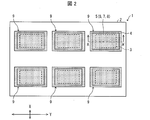
- FIG. 2 is a plan view of the substrate 1 of the organic EL display device according to Embodiment 1 of the present invention.
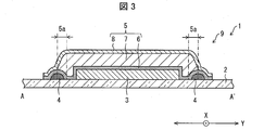
- FIG. 3 is a cross-sectional view of an organic EL display panel formation region of the substrate of FIG. FIG. 2 shows a configuration in which six organic EL display panels are cut from a single mother glass. Note that the number of chamfered organic EL display panels from one mother glass is not limited to six, and may be five or less, or seven or more.
- the substrate 1 has six organic EL display panel forming regions 9 disposed thereon.
- the organic EL display panel forming region 9 is a region that becomes an organic EL display device after being cut into pieces by being cut out from the mother glass.
- the substrate 1 has a TFT substrate 2, a pixel formation region 3, a frame bank 4, and a sealing layer 5.
- the TFT substrate 2 is manufactured in the TFT step S11.
- the TFT substrate 2 is provided with a pixel driving TFT (transistor, driving element), gate wiring and source wiring, and various other wirings on a mother glass by a known method, a passivation film (protective film), and interlayer insulation It is manufactured by forming a film (planarization film) or the like.
- the passivation film protects the TFT by preventing the metal film from peeling off the TFT.
- the passivation film is formed on the mother glass or through another layer, and covers the TFT.
- the passivation film is an inorganic insulating film made of silicon nitride, silicon oxide, or the like.
- the interlayer insulating film flattens the unevenness on the passivation film.
- the interlayer insulating film is formed on the passivation film.
- the interlayer insulating film is an organic insulating film made of a photosensitive resin such as acrylic or polyimide.
- a reflective electrode and an organic EL layer are formed on each pixel of the TFT substrate 2.
- a transparent electrode facing the reflective electrode through the organic EL layer is formed so as to cover the organic EL layer.
- a pixel formation region 3 is formed in which pixels are arranged in a matrix in a region for displaying an image.
- a frame bank 4 surrounding the pixel formation region 3 in a frame shape is also formed on the TFT substrate 2.
- the frame bank 4 is made of a photosensitive resin such as acrylic or polyimide. By forming the frame-like bank 4 from acrylic, the film thickness can be formed as thick as 1.0 ⁇ m or more, for example. Further, the frame-like bank 4 may be covered with an inorganic film such as a nitride film.
- the sealing layer 5 is formed.
- the sealing layer 5 can have a three-layer structure in which an inorganic film, an organic film, and an inorganic film are stacked in this order.
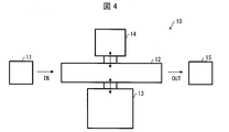
- FIG. 4 is a diagram showing an outline of the sealing system 10 that forms the sealing layer 5.
- the sealing system 10 is an example of a device group for forming the sealing layer 5.
- the sealing system 10 includes a first CVD device 11, a substrate transport robot 12, an inkjet coating device 13, a leveling device 14, and a second CVD device 15.
- the substrate 1 transported from the organic EL step S12 is first subjected to an inorganic film made of silicon nitride, silicon oxide, or the like in the region surrounded by the frame bank 4 including at least the frame bank 4 by the first CVD apparatus 11. A film 6 is formed. Next, the substrate on which the inorganic film 6 is formed is carried into the inkjet coating apparatus 13 via the substrate transport robot 12.
- an ink material containing a photosensitive material such as an acrylic resin, an epoxy resin, or polyimide is applied to the region on the inorganic film 6 and surrounded by the frame-shaped bank 4 by the ink jet coating apparatus 13.
- the frame bank 4 functions as a bank for damming the ink material.
- the substrate on which the ink material is applied is carried into the leveling device 14 via the substrate transport robot 12.
- the substrate on which the ink material is applied is left on the substrate mounting stage for a predetermined time.
- the ink material on the substrate flows and flattens.
- the ink material on the substrate is irradiated with UV light from a UV light source disposed in the leveling device 14. Thereby, the ink material is cured and an organic film 7 is formed on the inorganic film 6.
- the substrate on which the organic film 7 is formed is carried into the second CVD apparatus 15 via the substrate transfer robot 12.
- an inorganic film 8 made of silicon nitride or silicon oxide is formed by the second CVD apparatus 15 so as to cover the organic film 7 and the inorganic film 6.
- the flat sealing layer 5 is formed as shown in FIG.
- the organic EL layer formed in the pixel formation region 3 by the sealing layer 5 is thin-film sealed (TFE: Thin Film Encapsulation), thereby preventing the organic EL layer from being deteriorated by moisture or oxygen entering from the outside.
- TFE Thin Film Encapsulation
- each organic EL display panel forming region 9 is cut into individual pieces. Thereby, an organic EL display device is completed.
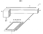
- FIG. 5 is a diagram illustrating a schematic configuration of the inkjet coating apparatus 13.
- the inkjet coating apparatus 13 includes a substrate mounting stage 41 on which the substrate 1 is mounted, an inkjet head 42 that drops an ink material that becomes the organic film 7, and a head support portion 43 that supports the inkjet head 42 movably.
- the substrate mounting stage 41 moves in the Y axis direction.
- the inkjet head 42 moves in the X axis direction orthogonal to the Y axis direction.
- the substrate placement stage 41 moves relative to the inkjet head 42.
- the substrate mounting stage 41 moves in the Y-axis direction. That is, the Y-axis direction is the direction in which the ink material is applied to the substrate 1.
- an ink material is applied from the inkjet head 42 onto the substrate 1 mounted on the substrate mounting stage 41.
- the inkjet head 42 moves a predetermined distance in the X-axis direction, and the substrate mounting stage 41 moves again in the Y-axis direction.
- the ink material is applied to all of the predetermined areas on 1.
- the ink material may be leveled by allowing the substrate 1 to stand on the substrate mounting stage 41 for a predetermined time, and then unloaded from the ink jet coating device 13. You may carry out from the inkjet coating device 13 immediately.
- the substrate mounting stage 41 includes a substrate mounting portion 30 to be described later in a region where the substrate 1 is mounted.
- the substrate mounting stage 41 may include any of the substrate mounting portions 30A to 30C described in the second to fourth embodiments, instead of the substrate mounting portion 30.
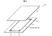
- FIG. 6 is a diagram illustrating a schematic configuration of the leveling device 14.
- the leveling device 14 also serves as an ink curing device that cures the ink material applied by the ink jet method.
- the leveling device 14 includes a substrate mounting stage 21 and a UV light source 22. In the case where an ink curing device is provided separately from the leveling device 14, the leveling device 14 may not have the UV light source 22.
- the substrate 1 coated with the ink material is transported from the substrate transport robot 12 by the ink jet coating device 13, the substrate 1 is mounted on the substrate mounting stage 21. And the board
- substrate 1 is left still only for predetermined time, such as 3 minutes. Thereby, the ink material applied to the substrate 1 is flattened by flowing.
- the UV light source 22 When a predetermined time has elapsed, the UV light source 22 is turned on and the ink material of the substrate 1 is irradiated with UV light. Thereby, the ink material of the substrate 1 is cured and the organic film 7 is formed.
- the substrate 1 when irradiating the substrate 1 with UV light, it is preferable to take a measure for reducing unevenness of curing such as irradiating the substrate 1 with air by floating the substrate 1 with air.
- the substrate 1 After the ink material is cured to form the organic film 7, the substrate 1 is unloaded from the leveling device 14 and is loaded into the second CVD device 15, which is a subsequent process, via the substrate transfer robot 12.
- the substrate mounting stage 21 is preferably provided with a substrate mounting portion 30 to be described later in a region where the substrate 1 is mounted.
- the substrate mounting stage 21 may include any of the substrate mounting portions 30A to 30C described in the second to fourth embodiments instead of the substrate mounting portion 30.
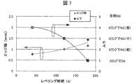
- FIG. 7 is a diagram showing the relationship between the width of the edge of the sealing layer of the organic EL display device manufactured by the conventional manufacturing method, and the unevenness of the display unit and the leveling time.
- the organic EL display device manufactured by a conventional manufacturing method is an organic EL display device in which a sealing layer is formed by an inkjet coating apparatus and a leveling apparatus that do not include the substrate mounting portion 30.
- the edge width shown in FIG. 7 is the width of the edge of the sealing layer. As shown in FIG. 7, when the leveling time of the ink material becomes long, the ink in the display portion is flattened, and display unevenness due to nonuniform ink film thickness becomes difficult to see. However, the edge width becomes large because the shape of the edge portion becomes gentle by leveling. Note that the unevenness shown in FIG. 7 represents the result of visual confirmation by irradiating the substrate with a green lamp.
- the edge portion maintains a steep shape, the edge width becomes small.
- the sealing layer is formed by the inkjet coating device 13 or the leveling device 14 provided with the substrate mounting portion 30, thereby shortening the leveling time and reducing the edge width and reducing the display unevenness. It becomes possible to do.
- the substrate mounting unit 30 may be provided on both the substrate mounting stage 41 of the inkjet coating device 13 and the substrate mounting stage 21 of the leveling device 14, or may be provided on only one of them.
- the substrate mounting unit 30 may be provided on at least one of the substrate mounting stages 21 and 41.
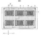
- FIG. 8 is a plan view showing the configuration of the substrate mounting unit 30.
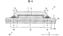
- FIG. 9 is a cross-sectional view of the vicinity of the organic EL display panel forming region 9 before the ink material 7a is cured on the substrate 1 mounted on the substrate mounting portion 30.
- FIG. FIG. 10 is a cross-sectional view of the vicinity of the organic EL display panel forming region 9 after the ink material 7a is cured on the substrate 1 mounted on the substrate mounting portion 30.
- FIG. 8 shows an example in which the substrate mounting unit 30 is provided on the substrate mounting stage 41.
- the direction indicated by the arrow is the scanning direction of the inkjet head (the direction in which the ink material 7a is applied).
- the substrate mounting unit 30 is arranged in a matrix form with the temperature control units 39 arranged in a matrix form spaced apart from each other.
- the substrate mounting unit 30 inquires the look-up table for information on the substrate 1 (panel model number, frame bank position, pixel formation region position, application direction, etc.) and information on the substrate 1. Based on the above, the temperature of the temperature adjustment unit 39 is adjusted.
- the lift pins 37 that lift up the substrate 1 when the substrate 1 is transported are arranged at the four corners of the substrate mounting portion 30.
- temperature adjusting elements 31 are arranged in a matrix on a stage base material 30a made of a metal material.
- the temperature adjusting elements 31 adjacent in the X direction and the Y direction are arranged on the entire surface of the substrate mounting portion 30 which is a region where the substrate 1 is placed. Each temperature adjustment element 31 can be individually adjusted in temperature.
- the temperature adjustment element 31 may be set to various sizes according to the size of the substrate 1. As an example, the temperature adjustment element 31 can be about 1 mm square.
- the temperature adjustment element 31 may be a heat source that can be adjusted and maintained so as to have two different temperatures. In the present embodiment, the temperature adjustment element 31 is a Peltier element.
- the temperature adjusting element 31 in the place where the organic EL display panel forming region 9 of the substrate 1 is arranged is a temperature adjusting portion 39.
- the region where the pixel formation region 3 is arranged in the substrate 1 constitutes a high temperature portion 33 having a temperature higher than the ambient temperature, and the region where the frame bank 4 is arranged is higher than the ambient temperature.
- the low temperature part 34 with low temperature is comprised.
- the substrate mounting unit 30 forms the temperature adjusting unit 39 so as to overlap the organic EL display panel forming region 9.
- the ambient temperature is the temperature around the board mounting portion 30. That is, the temperature around the substrate mounting stage 21 or the substrate mounting stage 41 provided with the substrate mounting unit 30.
- the atmospheric temperature is, for example, a temperature of about 20 ° C. or higher and 25 ° C. or lower.
- the high temperature part 33 is composed of a plurality of temperature adjusting elements 31.
- the temperature adjustment element 31 is about 30 degreeC or more and 60 degrees C or less as an example.
- the low temperature part 34 is composed of a plurality of temperature adjusting elements 31.
- the temperature adjustment element 31 is about 10 degreeC or more and 25 degrees C or less as an example.
- the maximum temperature of the low temperature part 34 may be the ambient temperature.
- the organic EL display panel forming region 9 is arranged in a matrix on the substrate 1 mounted on the substrate mounting unit 30.
- the organic EL display panel forming region 9 includes a pixel forming region 3 in which pixels are arranged in a matrix, a frame bank 4 surrounding the pixel forming region 3 in a frame shape, and a pixel in the frame bank 4.
- An ink material 7a applied by an inkjet application device 13 is disposed so as to cover the formation region 3.
- the substrate mounting unit 30 includes a temperature adjustment unit 39 that is temperature-adjusted and arranged in a matrix. And the temperature adjustment part 39 has the low temperature part 34 and the high temperature part 33 by which temperature adjustment was carried out.
- the low temperature part 34 is arranged in a frame shape at a position corresponding to the frame bank 4 and has a first temperature that is equal to or lower than the ambient temperature. That is, the low temperature part 34 is disposed at a position overlapping the frame bank 4.
- the ink material 7a is dropped from the nozzle of the inkjet head 42 and applied to the substrate 1, the flow of the ink material 7a in the vicinity of the frame bank 4 can be suppressed. As a result, it is possible to prevent the ink from going over the frame-like bank 4 and, as shown in FIG. 10, in the organic layer 7 in which the ink material 7 a is cured, the edge 7 b that is a portion having a different film thickness. The width can be reduced.
- variety of the edge part 5a which is a part from which a film thickness differs can be formed by forming the inorganic layer 8 on the organic layer 7.
- the high-quality sealing layer 5 can be formed by the ink jet method. Further, it is possible to form an organic EL display device in which the width of the frame region around the pixel formation region 3 is small.
- the high temperature portion 33 is disposed in a region corresponding to the pixel formation region 3 in the region surrounded by the low temperature portion 34. That is, the high temperature part 33 is disposed at a position overlapping the pixel formation region 3. And the high temperature part 33 is 2nd temperature higher than atmospheric temperature. That is, the high temperature part 33 is adjusted to be higher in temperature than the low temperature part 34.
- the ink material 7a applied to the substrate 1 heat is applied to a portion covering the pixel formation region 3, whereby flow is promoted and flattening of the ink material 7a is promoted.
- the time concerning the planarization process of the ink material 7a can be shortened. That is, the leveling time of the ink material 7a can be shortened.
- a flat organic film 7 can be formed in a short time.
- the flat sealing layer 5 can be formed by forming the inorganic layer 8 on the organic layer 7.
- the substrate mounting portion 30 is provided with temperature adjusting elements 31 that are arranged in a matrix and can be set to the first temperature and the second temperature.
- the temperature adjustment element 31 is disposed on substantially the entire surface other than the region where the lift pins 37 are disposed.
- a Peltier element can be used as an example of the temperature adjustment element 31, a Peltier element can be used.
- the temperature adjustment element 31 constituting the high-temperature part 33 various heating mechanisms such as a heating mechanism that heats a resistor by flowing current can be used in addition to the Peltier element.
- a Peltier element it is preferable to use a Peltier element as the temperature adjustment element 31. This is because both the temperature adjustment element 31 constituting the high temperature part 33 and the temperature adjustment element 31 constituting the low temperature part 34 can be constituted by Peltier elements, which is efficient.
- the temperature adjusting element 31 at a necessary location can be set to the first temperature or the second temperature, and the low temperature part 34 and the high temperature part 33 can be provided. For this reason, the board
- the substrate mounting unit 30 has been described as having the low temperature part 34 and the high temperature part 33, but the substrate mounting part 30 may have only the low temperature part 34 without the high temperature part 33.
- the lift pins 37 may be arranged not only at the four corners of the substrate 1 in the substrate mounting portion 30 but also at positions that overlap with the area where the ink material 7a is applied. Therefore, when the substrate mounting portion 30 is provided on the substrate mounting stage 21 and the leveling device also serves as the ink curing device, the surface of the lift pin 37 is not changed so that the reflectance of the UV light does not change at the position of the lift pin 37. It is preferable to apply the same plating as the surface of the stage portion or a PI (polyimide) material having a UV reflectance equivalent to the surface of the substrate mounting portion 30 to make the reflectance uniform within the ink material application region.
- PI polyimide
- FIG. 11 is a plan view illustrating a configuration of a substrate mounting portion 30A according to the second embodiment of the present invention.
- FIG. 12 is a cross-sectional view of the vicinity of the organic EL display panel formation region in the substrate 1 mounted on the substrate mounting portion 30A.
- FIG. 14 is a cross-sectional view of the vicinity of the organic EL display panel forming region 9 after the ink material 7a is cured on the substrate 1 mounted on the substrate mounting portion 30A.
- the direction indicated by the arrow (the direction from the right to the left in the drawing) is the scanning direction of the inkjet head (the direction in which the ink material 7a is applied).
- a substrate mounting portion 30A may be provided on at least one of the substrate mounting stage 41 of the inkjet coating device 13 (FIG. 5) and the substrate mounting stage 21 of the leveling device 14 (FIG. 6).
- the substrate mounting portion 30A has a configuration in which a heat insulating portion 32 is arranged between the temperature adjusting elements 31 arranged in a matrix in the substrate mounting portion 30.
- Other configurations of the substrate mounting unit 30A are the same as those of the substrate mounting unit 30.
- the heat insulating portion 32 is provided in a lattice shape around the temperature adjusting element 31.
- the heat insulation part 32 can be comprised from air, water, and another heat insulation material.
- the heat insulating portion 32 may be a groove recessed from the surface of the substrate mounting portion 30A (the mounting surface of the substrate 1).
- the heat insulation part 32 may have a water-cooled heat insulation mechanism.
- FIG. 13 is a diagram showing a schematic configuration of the water-cooled heat insulation part 32.
- the heat insulating part 32 includes an inflow pipe 32 a, a circulation part 32 b, and a discharge pipe 32 c, and the circulation part 32 b surrounds the temperature adjustment element 31.
- the inflow pipe 32a and the discharge pipe 32c are connected to the circulation part 32b.
- the temperature adjustment element 31 and the circulation part 32b are in contact.
- the temperature adjusting element 31 and the circulation part 32b may be separated from each other.
- the water that has flowed into the circulation part 32b from the inflow pipe 32a circulates in the circulation part 32b, goes around the temperature adjusting element 31, and is discharged from the discharge pipe 32c. In this way, it is possible to insulate between the adjacent temperature adjusting elements 31.
- the heat insulating portion 32 is configured by a water-cooling method
- the configuration may be such that water can flow to any location in the lattice-shaped heat insulating portion 32.
- the low temperature part 34 and the high temperature part 33 are insulated by circulating water through the heat insulation part 32 between the low temperature part 34 and the high temperature part 33. Thereby, the low temperature part 34 can be accurately maintained at the first temperature and the high temperature part 33 can be maintained at the second temperature with high accuracy.
- the low temperature portion 34 is disposed at a position overlapping the frame-like bank 4.
- the ink material 7a is dropped from the nozzle of the inkjet head 42 and applied to the substrate 1, the flow of the ink material 7a in the vicinity of the frame bank 4 can be suppressed. As a result, it is possible to prevent the ink from going over the frame-shaped bank 4 and, as shown in FIG. 14, the organic layer 7 having the cured ink material 7a has an edge portion 7b which is a portion having a different film thickness. The width can be reduced.
- variety of the edge part 5a which is a part from which a film thickness differs can be formed by forming the inorganic layer 8 on the organic layer 7.
- the high temperature portion 33 is disposed at a position overlapping the pixel formation region 3. And the high temperature part 33 is 2nd temperature higher than atmospheric temperature.
- the ink material 7a applied to the substrate 1 heat is applied to a portion covering the pixel formation region 3, whereby flow is promoted and flattening of the ink material 7a is promoted. Thereby, the time concerning the planarization process of the ink material 7a can be shortened. As a result, as shown in FIG. 14, the flat organic film 7 can be formed in a short time.
- the flat sealing layer 5 can be formed by forming the inorganic layer 8 on the organic layer 7.
- FIG. 15 is a plan view illustrating a configuration of a substrate mounting portion 30B according to the third embodiment of the present invention.
- FIG. 16 is a cross-sectional view of the vicinity of the organic EL display panel formation region on the substrate mounted on the substrate mounting portion 30B.
- FIG. 17 is a cross-sectional view of the vicinity of the organic EL display panel formation region 9 after the ink material 7a is cured on the substrate 1 mounted on the substrate mounting portion 30B.
- the direction indicated by the arrow (the direction from the right to the left in the drawing) is the scanning direction of the inkjet head (the direction in which the ink material 7a is applied).
- a substrate mounting portion 30B may be provided on at least one of the substrate mounting stage 41 of the inkjet coating device 13 (FIG. 5) and the substrate mounting stage 21 of the leveling device 14 (FIG. 6).
- the substrate mounting portion 30B has temperature adjusting portions 39B that are temperature-adjusted and arranged in a matrix.
- the temperature adjustment unit 39B includes a low temperature part 34B and a high temperature part 33B that are temperature adjusted.
- the stage base material 30a which is the metal material which comprises the board
- the high temperature portion 33B is disposed in a region surrounded by the low temperature portion 34B and corresponding to the pixel formation region 3, and is adjusted to the second temperature.
- the high temperature part 33B has a heating mechanism such as a metal plate and a thermoelectric element for heating the metal plate.
- the low temperature part 34B is arranged in a frame shape at a position corresponding to the frame bank 4 and is adjusted to the first temperature.
- the low temperature part 34B can be comprised from air, water, and another heat insulation material.
- the low temperature part 34B may be a groove recessed from the surface of the substrate mounting part 30B (the mounting surface of the substrate 1).
- FIG. 18 is a diagram showing a schematic configuration of the water cooling type low temperature part 34B.
- the low temperature part 34B includes an inflow pipe 34Ba, a circulation part 34Bb, and a discharge pipe 34Bc.
- the circulation part 34Bb surrounds the high temperature part 33Bc while being separated from the high temperature part 33B.
- the inflow pipe 34Ba and the discharge pipe 34Bc are connected to the circulation portion 34Bb.
- the water that has flowed into the circulation part 34Bb from the inflow pipe 34Ba passes through the circulation part 34Bb, goes around the high temperature part 33B, and is discharged from the discharge pipe 34Bc. In this manner, the vicinity of the frame bank 4 in the substrate 1 can be cooled.
- the ink material 7a is dropped from the nozzle of the inkjet head 42 and applied to the substrate 1, the flow of the ink material 7a in the vicinity of the frame bank 4 can be suppressed.
- the edge 7b which is a portion having a different film thickness, in the organic layer 7 in which the ink material 7a is cured. The width can be reduced.
- variety of the edge part 5a which is a part from which a film thickness differs can be formed by forming the inorganic layer 8 on the organic layer 7.
- FIG. According to this, the high quality sealing layer 5 can be formed by the inkjet method. Further, it is possible to form an organic EL display device in which the width of the frame region around the pixel formation region 3 is small.
- the high temperature portion 33 ⁇ / b> B is disposed at a position overlapping the pixel formation region 3.
- the high temperature part 33B is 2nd temperature higher than atmospheric temperature.
- the ink material 7a applied to the substrate 1 heat is applied to a portion covering the pixel formation region 3, whereby flow is promoted and flattening of the ink material 7a is promoted. Thereby, the time concerning the planarization process of the ink material 7a can be shortened. As a result, as shown in FIG. 17, the flat organic film 7 can be formed in a short time.
- the flat sealing layer 5 can be formed by forming the inorganic layer 8 on the organic layer 7.
- FIG. 19 is a diagram illustrating a substrate mounting portion and a set temperature according to the fourth embodiment of the present invention.
- FIG. 19A is a cross-sectional view illustrating a configuration of a substrate mounting portion 30C according to Embodiment 4 of the present invention
- FIG. 19B is an example of a first temperature gradient in the substrate mounting portion 30C illustrated in FIG. (C) is a figure showing the example of the 2nd temperature gradient of 30 C of board
- a substrate mounting portion 30C may be provided on at least one of the substrate mounting stage 41 of the inkjet coating device 13 (FIG. 5) and the substrate mounting stage 21 of the leveling device 14 (FIG. 6).
- the substrate mounting part 30C has a configuration in which a temperature gradient is given to the high temperature part 33 in the substrate mounting part 30 (FIGS. 8 and 9).
- the direction indicated by the arrow is the scanning direction of the inkjet head (the direction of applying the ink material 7a).
- the ink material 7a applied by the inkjet application device 13 has a height at an application start position 7as and an application end position 7ae immediately after application. Different.
- the height tends to be lower due to the effect of leveling due to the stay.
- the temperature adjustment element 31b and the temperature adjustment are sequentially performed from the side closer to the application start position 7as to the side closer to the application end position 7ae.
- An element 31c, a temperature adjustment element 31d, and a temperature adjustment element 31e are used.
- a temperature adjustment element near the temperature adjustment element 31b is a temperature adjustment element 31a
- a temperature adjustment element near the temperature adjustment element 31e is a temperature adjustment element 31f.
- each temperature adjustment is performed so as to have a temperature gradient from the temperature adjustment element 31b to the temperature adjustment element 31e (that is, in the scan direction of the inkjet head).
- the temperature of the element 31 is adjusted.
- the height of the ink material immediately after the application depends on the viscosity of the ink material, a set value for applying the ink jet application device 13, and the like.
- FIG. 19B shows an example in which a temperature gradient is provided so that the temperature near the application start position 7as is higher than the temperature near the application end position 7ae.
- the leveling speed of the ink material 7a can be improved by adjusting the temperature of the high temperature portion 33 from the application start position 7as to the temperature corresponding to the height of the ink material 7a at the application end position 7ae.
- the temperature ts ⁇ te of the high temperature portion 33 (temperature adjusting elements 31b to 31e) facing the pixel formation region 3 is larger than the ambient temperature, and the low temperature portion 34 facing the frame bank 4 is.
- the temperature tb of the (temperature training elements 31a and 31f) is equal to or lower than the ambient temperature.
- the central temperature tc is relatively increased (for example, the temperature of the temperature adjusting elements 31c and 31d is increased), and the temperature of the edge portion is increased.
- the ts ⁇ te may be set lower than the temperature tc (for example, the temperature of the temperature adjusting elements 31b and 31f is lowered).
- the ink material 7a in the vicinity of the center of the pixel formation region 3 can be flowed and flattened. Further, the flow of the edge portion of the pixel formation region 3 is relatively suppressed as compared to the vicinity of the center, and the flow of ink in the vicinity of the low temperature portion 34 can be easily suppressed. For this reason, it can suppress more reliably that the ink material 7a gets over the frame-shaped bank 4. FIG.
- the temperatures tc, ts, and te of the high temperature portion 33 (temperature adjusting elements 31b to 31e) facing the pixel formation region 3 are larger than the ambient temperature, and the low temperature facing the frame bank 4 is low.
- the temperature tb of the part 34 (temperature training elements 31a and 31f) is equal to or lower than the ambient temperature.
- the substrate mounting portion 30C shown in FIGS. 19A, 19B and 19C also forms the flat organic layer 7 in which the width of the edge portion 7b is narrow, similarly to the organic layer 7 shown in FIG. can do.
- the flat sealing layer 5 having a narrow width of the edge portion 5a can be formed.
- the high temperature portions 33A and 33B may have a temperature gradient according to the height from the application start position 7as to the application end position 7ae of the ink material 7a.
- the substrate mounting stage is a substrate mounting stage on which a substrate in which organic EL display panel formation regions are arranged in a matrix is mounted, and pixels are arranged in a matrix in the organic EL display panel formation region.
- the substrate mounting stage has a temperature-adjusted temperature-adjusted portion arranged in a matrix, and the temperature-adjusted portion is arranged in a frame shape at a position corresponding to the frame-shaped bank. And having a low temperature portion which is a first temperature equal to or lower than the ambient temperature.
- the flow of the ink material in the vicinity of the frame bank can be suppressed after the ink material is applied.
- a high quality film can be formed by the ink jet method.
- the substrate mounting stage according to aspect 2 of the present invention is the substrate mounting stage according to aspect 1, wherein the temperature adjustment unit is disposed in a region surrounded by the low temperature part and corresponding to the pixel formation region, and the ambient temperature You may have the high temperature part which is higher 2nd temperature.
- the flow of the ink material covering the pixel formation region is promoted, and the flattening of the ink material is promoted.
- the time concerning the planarization process of the said ink material can be improved.
- a substrate mounting stage according to aspect 3 of the present invention is arranged in a matrix form in the aspect 2 and includes temperature adjustment elements that are the first temperature, and the low temperature portion is configured by a plurality of the temperature adjustment elements. It may be.
- the low temperature part can be set according to the shape of the frame bank. For this reason, a highly versatile substrate mounting stage can be obtained.
- a substrate mounting stage according to aspect 4 of the present invention is the substrate mounting stage according to aspect 2, which is arranged in a matrix and includes temperature adjusting elements that are the first temperature or the second temperature, and the low temperature part and the high temperature part are: Each may be constituted by a plurality of the temperature adjusting elements.
- the low temperature part and the high temperature part can be set in accordance with the shape of the frame bank and the pixel formation region. For this reason, a highly versatile substrate mounting stage can be obtained.
- a heat insulating part may be disposed between the low temperature part and the high temperature part. According to the above configuration, the low temperature part can be accurately maintained at the first temperature and the high temperature part can be maintained at the second temperature with high accuracy.
- the heat insulating part may be provided in a lattice shape around the temperature adjusting element, and may have a circulating part through which a fluid flows.
- a substrate mounting stage according to aspect 7 of the present invention is the substrate mounting stage according to aspect 5, wherein the heat insulating portion is provided in a lattice shape around the temperature adjusting element, and has a groove shape recessed from the surface of the substrate mounting stage. You may do it.
- the substrate mounting stage according to Aspect 8 of the present invention is the substrate mounting stage according to Aspects 2, 4 to 7, wherein the high temperature portion is temperature-adjusted so as to have a temperature gradient from the ink material application start position to the application end position by the inkjet method. May be.
- the temperature of the high temperature part can be adjusted to a temperature corresponding to the height of the ink material at the application end position from the application start position. Thereby, the time concerning the planarization process of the said ink material can be improved.
- the high temperature part may have a higher temperature in the center of the pixel formation region than in the application start position.
- the temperature of the high temperature portion is higher in the center of the pixel formation region than in the application start position and the application end position. Also good.
- the temperature adjusting element may be composed of a Peltier element.
- the ink jet coating apparatus may include the substrate mounting stage according to the first to eleventh aspects and apply the ink material.
- the leveling coating apparatus may include the substrate mounting stage according to the first to eleventh aspects, and may planarize the ink material.
- a method for manufacturing an organic EL display device is a method for manufacturing an organic EL display device that manufactures an organic EL display device from a substrate in which organic EL display panel formation regions are arranged in a matrix.
- the organic EL display panel formation region includes a pixel formation region in which pixels are arranged in a matrix, a frame bank surrounding the pixel formation region in a frame shape, and the pixel formation region in the frame bank.
- An ink material before curing applied by an inkjet method is arranged to cover, After the ink material is applied by an ink jet method, the method includes a temperature adjustment step of adjusting a position corresponding to the frame-shaped bank on the substrate to a first temperature that is equal to or lower than an ambient temperature.
- a position corresponding to the pixel formation region in the substrate is further set to a second temperature higher than the ambient temperature. It is preferable to adjust to.
Landscapes
- Engineering & Computer Science (AREA)
- Manufacturing & Machinery (AREA)
- Microelectronics & Electronic Packaging (AREA)
- Electroluminescent Light Sources (AREA)
Abstract
基板搭載部30は、基板(1)の画素形成領域(3)を囲む枠状バンク(4)に対応する位置に、雰囲気温度以下に調整された低温部(34)を有することを特徴とする。これにより、封止層の縁の幅を狭める。
Description
本発明は、基板搭載ステージ、インクジェット塗布装置、レベリング装置および有機EL表示装置の製造方法に関する。
特許文献1には、基板搭載ステージに、搭載した基板を加熱する機構を設ける構成が記載されている。
有機EL表示装置において、画素の有機EL層を封止するために、画素形成領域全面に封止層が形成される。封止層は、画素形成領域を枠状に囲む枠状バンクを形成後、当該枠状バンク内にインクジェット法によりインク材を塗布し、当該インク材を硬化させる。このとき、平坦な封止層を形成するために、塗布されたインク材を硬化させる前に平坦化(レベリング)させる。しかしこのインク材をレベリングさせるときに、枠状バンク近傍の温度が高いと、インクが枠状バンクを乗り越えて広がりやすくなり、また、膜厚が不均一な封止層の縁の部分の幅が広くなるため、狭額縁化することができない。
本発明は、上記従来の問題点に鑑みなされたものであって、その目的は、封止層の縁の幅を狭めることである。
上記の課題を解決するために、本発明の一態様に係る基板搭載ステージは、有機EL表示パネル形成領域がマトリクス状に配置された基板を搭載する基板搭載ステージであって、上記有機EL表示パネル形成領域には、画素がマトリクス状に配置された画素形成領域と、当該画素形成領域を枠状に囲む枠状バンクと、当該枠状バンク内であって上記画素形成領域を覆うようにインクジェット法により塗布された硬化前のインク材とが配置されており、上記基板搭載ステージは、温度調整がされマトリクス状に配置された温度調整部を有し、上記温度調整部は、上記枠状バンクに対応する位置に枠状に配置され、雰囲気温度以下の第1温度である低温部を有することを特徴とする。
上記の課題を解決するために、本発明の一態様に係る有機EL表示装置の製造方法は、有機EL表示パネル形成領域がマトリクス状に配置された基板から有機EL表示装置を製造する有機EL表示装置の製造方法であって、上記有機EL表示パネル形成領域には、画素がマトリクス状に配置された画素形成領域と、当該画素形成領域を枠状に囲む枠状バンクと、当該枠状バンク内であって上記画素形成領域を覆うようにインクジェット法により塗布された硬化前のインク材とが配置されており、上記インク材がインクジェット法にて塗布された後、上記基板における上記枠状バンクに対応する位置を、雰囲気温度以下である第1温度に調整する温度調整工程を含むことを特徴とする。
本発明の一態様によれば、封止層の縁の幅を狭めることができるという効果を奏する。
〔実施形態1〕
本発明の実施形態1について、図1~図9に基づいて説明する。
本発明の実施形態1について、図1~図9に基づいて説明する。
(有機EL表示装置の製造方法の概略)
図1は、本発明の実施形態1に係る有機EL表示装置の製造工程を表す図である。図2は本発明の実施形態1に係る有機EL表示装置の基板1の平面図である。図3は図2の基板の有機EL表示パネル形成領域の断面図である。図2では、1枚のマザーガラスから有機EL表示パネルを6面取りする場合の構成を示している。なお、1枚のマザーガラスから有機EL表示パネルを面取りする個数は6つに限らず、5つ以下、または7つ以上であってもよい。
図1は、本発明の実施形態1に係る有機EL表示装置の製造工程を表す図である。図2は本発明の実施形態1に係る有機EL表示装置の基板1の平面図である。図3は図2の基板の有機EL表示パネル形成領域の断面図である。図2では、1枚のマザーガラスから有機EL表示パネルを6面取りする場合の構成を示している。なお、1枚のマザーガラスから有機EL表示パネルを面取りする個数は6つに限らず、5つ以下、または7つ以上であってもよい。
基板1には有機EL表示パネル形成領域9が6つ配置されている。有機EL表示パネル形成領域9は、マザーガラスから切り出されることで個片化された後、有機EL表示装置となる領域である。
基板1は、TFT基板2と、画素形成領域3と、枠状バンク4と、封止層5とを有する。
まず、TFT工程S11においてTFT基板2を作製する。TFT基板2は、マザーガラスに、公知の方法により、画素駆動用のTFT(トランジスタ、駆動素子)、ゲート配線およびソース配線、その他各種の配線が形成され、パッシベーション膜(保護膜)、および層間絶縁膜(平坦化膜)などが形成されることで作製される。
パッシベーション膜はTFTにおける金属膜の剥離を防止し、TFTを保護する。パッシベーション膜はマザーガラス上又は他の層を介して形成されており、TFTを覆っている。パッシベーション膜は、窒化シリコンや酸化シリコンなどからなる無機絶縁性膜である。
層間絶縁膜は、パッシベーション膜上の凹凸を平坦化する。層間絶縁膜はパッシベーション膜上に形成されている。層間絶縁膜はアクリルまたはポリイミドなどの感光性樹脂からなる有機絶縁膜である。
次に、有機EL工程S12において、TFT基板2の各画素に、反射電極、有機EL層を形成する。そして、有機EL層を介して反射電極と対向する透明電極を、有機EL層を覆うように形成する。これにより、画像を表示する領域に画素がマトリクス状に配置された画素形成領域3が形成される。また、この画素形成領域3を形成する際に、当該画素形成領域3を枠状に囲む枠状バンク4もTFT基板2上に形成する。枠状バンク4は、アクリルまたはポリイミドなどの感光性樹脂からなる。枠状バンク4をアクリルから構成することで、膜厚を、例えば、1.0μm以上と厚く形成することができる。また、枠状バンク4上を窒化膜などの無機膜で覆ってもよい。
そして、次に、封止工程S13において、封止層5を形成する。封止層5は、一例として、無機膜、有機膜、および無機膜がこの順に積層された3層構造とすることができる。
図4は、封止層5を形成する封止システム10の概略を表す図である。封止システム10は、封止層5を形成するための装置群の一例である。
封止システム10は、第1CVD装置11と、基板搬送ロボット12と、インクジェット塗布装置13と、レベリング装置14と、第2CVD装置15とを有する。
有機EL工程S12から搬送されてきた基板1に、まず、第1CVD装置11によって、少なくとも枠状バンク4上を含め枠状バンク4で囲まれた領域内に、窒化シリコンまたは酸化シリコンなどからなる無機膜6を成膜する。無機膜6が成膜された基板は、次に、基板搬送ロボット12を介して、インクジェット塗布装置13に搬入される。
そして、インクジェット塗布装置13によって、無機膜6上であって枠状バンク4で囲まれた領域内に、アクリル樹脂、エポキシ樹脂またはポリイミド等の感光性材料を含むインク材を塗布する。枠状バンク4は、このインク材を堰き止める土手として機能する。次に、インク材が塗布された基板は、基板搬送ロボット12を介して、レベリング装置14に搬入される。
そして、レベリング装置14において、インク材が塗布された基板は、所定時間、基板搭載ステージ上に静置する。これにより、基板上のインク材が流動し平坦化する。そして、所定時間経過後、レベリング装置14に配置されているUV光源からUV光を、基板上のインク材に照射する。これにより、インク材が硬化し無機膜6上に有機膜7が成膜される。
次に、有機膜7が成膜された基板は、基板搬送ロボット12を介して、第2CVD装置15へ搬入される。そして、第2CVD装置15によって、有機膜7および無機膜6を覆うように、窒化シリコンまたは酸化シリコンなどからなる無機膜8を成膜する。これにより、図3に示すように平坦な封止層5が形成される。
封止層5によって画素形成領域3に形成された有機EL層を薄膜封止(TFE:Thin Film Encapsulation)することで、外部から浸入した水分や酸素によって有機EL層が劣化するのを防止する。
この封止層5を形成した後、フレキシブル工程S14を設けてもよい。フレキシブル工程S14では、基板のガラスを剥離して支持体となるフィルムなどを貼る。
そして、各有機EL表示パネル形成領域9が切り出されることで個片化される。これにより有機EL表示装置が完成する。
(インクジェット塗布装置13)
図5は、インクジェット塗布装置13の概略構成を表す図である。インクジェット塗布装置13は、基板1を搭載する基板搭載ステージ41と、有機膜7となるインク材を滴下するインクジェットヘッド42と、インクジェットヘッド42を移動可能に支持するヘッド支持部43とを有する。
図5は、インクジェット塗布装置13の概略構成を表す図である。インクジェット塗布装置13は、基板1を搭載する基板搭載ステージ41と、有機膜7となるインク材を滴下するインクジェットヘッド42と、インクジェットヘッド42を移動可能に支持するヘッド支持部43とを有する。
基板載置ステージ41は、Y軸方向に移動する。インクジェットヘッド42はY軸方向と直交するX軸方向に移動する。
基板1が基板載置ステージ41に載置されると、インクジェットヘッド42に対して基板搭載ステージ41が相対移動する。本実施形態では基板搭載ステージ41はY軸方向に移動する。すなわち、Y軸方向が基板1に対するインク材の塗布方向である。
そして、インクジェットヘッド42から基板搭載ステージ41に搭載された基板1上にインク材が塗布される。
インクジェットヘッド42の幅と基板1の幅とに応じて、必要な場合は、インクジェットヘッド42がX軸方向に所定距離移動し、再度、基板搭載ステージ41がY軸方向に移動することで、基板1上の所定領域の全てにインク材が塗布される。
インク材の塗布が完了すると、基板搭載ステージ41上に基板1を所定時間静置することでインク材をレベリングした後、インクジェット塗布装置13から搬出してもよいし、インク材の塗布が完了したらすぐに、インクジェット塗布装置13から搬出してもよい。
基板搭載ステージ41は、基板1を搭載する領域に、後述する基板搭載部30を備えていることが好ましい。または、基板搭載ステージ41は、基板搭載部30に換えて、実施形態2~4において説明する基板搭載部30A~30Cの何れかを備えていてもよい。
(レベリング装置14)
図6は、レベリング装置14の概略構成を表す図である。本実施形態においては、レベリング装置14は、インクジェット法により塗布したインク材を硬化させるインク硬化装置も兼ねているものとする。
図6は、レベリング装置14の概略構成を表す図である。本実施形態においては、レベリング装置14は、インクジェット法により塗布したインク材を硬化させるインク硬化装置も兼ねているものとする。
レベリング装置14は、基板搭載ステージ21と、UV光源22とを有する。なお、レベリング装置14以外に別途、インク硬化装置を設ける場合は、レベリング装置14はUV光源22を有していなくてもよい。
基板搬送ロボット12から、インクジェット塗布装置13によってインク材が塗布された基板1が搬送されてくると、当該基板1は、基板搭載ステージ21に搭載される。そして、例えば3分など、所定時間だけ基板1は静置される。これにより、基板1に塗布されたインク材は流動することで平坦化される。
所定時間が経過したら、UV光源22を点灯させ、UV光を基板1のインク材に照射する。これにより、基板1のインク材が硬化し有機膜7が成膜される。なお、UV光を基板1に照射する際、エアーによって基板1を浮かび上がらせてUV光を基板1に照射するなどの硬化ムラ低減策を施すことが好ましい。インク材を硬化させて有機膜7を成膜後、基板1はレベリング装置14から搬出されて、基板搬送ロボット12を介して後工程である第2CVD装置15へ搬入される。
基板搭載ステージ21は、基板1を搭載する領域に、後述する基板搭載部30を備えていることが好ましい。または、基板搭載ステージ21は、基板搭載部30に換えて、実施形態2~4において説明する基板搭載部30A~30Cの何れかを備えていてもよい。
(封止層の縁の膜厚ムラ)
図7を用いて、本実施形態に係る基板搭載部30が解決しようとする課題について具体的に説明する。
図7を用いて、本実施形態に係る基板搭載部30が解決しようとする課題について具体的に説明する。
図7は、従来の製造方法によって製造した有機EL表示装置の封止層の縁の幅、および、表示部のムラとレベリング時間との関係を表す図である。従来の製造方法によって製造した有機EL表示装置とは、基板搭載部30を備えないインクジェット塗布装置およびレベリング装置によって封止層を形成した有機EL表示装置である。
図7に示すエッジ幅は、封止層の縁の幅である。図7に示すように、インク材のレベリング時間が長くなると表示部のインクが平坦化され、インク膜厚の不均一による表示ムラが目視され難くなる。しかしレベリングによりエッジ部の形状がなだらかになるため、エッジ幅は大きくなる。なお、図7に示すムラは、Greenランプを基板に照射して目視確認をした結果を表している。
一方、インク材のレベリング時間が短くなると表示部のインクが十分に平坦化されず、インク膜厚の不均一による表示ムラが目視で確認されやすくなる。しかしエッジ部は急峻な形状が保たれるため、エッジ幅は小さくなる。
そこで、後述するように、基板搭載部30を備えた、インクジェット塗布装置13またはレベリング装置14によって封止層を形成することで、レベリング時間を短縮してエッジ幅を小さく抑えつつ、表示ムラを低減することが可能になる。
(基板搭載部30の構成)
次に、図8~図10を用いて、インクジェット塗布装置13およびレベリング装置14のうち少なくとも一方が備える基板搭載部30の構成について説明する。
次に、図8~図10を用いて、インクジェット塗布装置13およびレベリング装置14のうち少なくとも一方が備える基板搭載部30の構成について説明する。
基板搭載部30は、インクジェット塗布装置13の基板搭載ステージ41と、レベリング装置14の基板搭載ステージ21の両方に設けられてもよいし、何れか一方にだけ設けられていてもよい。基板搭載部30は、基板搭載ステージ21・41のうち、少なくとも一方に設けられていればよい。基板搭載部30を基板搭載ステージ21・41の両方に設けることで、何れか一方にだけ設ける場合と比べてタクト短縮の効果を得ることができる。なお、実施形態2~4にて説明する基板搭載部30・30A~30Cにおいても同様である。
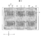
図8は、基板搭載部30の構成を表す平面図である。図9は、基板搭載部30に搭載された基板1におけるインク材7a硬化前の有機EL表示パネル形成領域9近傍の断面図である。図10は、基板搭載部30に搭載された基板1におけるインク材7a硬化後の有機EL表示パネル形成領域9近傍の断面図である。
なお、図8では、基板搭載部30が基板搭載ステージ41に設けられている例を示している。また、図9では、矢印に示す方向(紙面右から左へ向かう方向)がインクジェットヘッドのスキャン方向(インク材7aの塗布方向)である。
図8に示すように基板搭載部30は、マトリクス状に配置された温度調節部39が互いに離間しつつマトリクス状に配置されている。
基板搭載部30は、基板1の搭載前に、ルックアップテーブルに基板1の情報(パネルの型番、枠状バンクの位置、画素形成領域の位置、塗布方向など)を問い合わせ、その基板1の情報をもとに、温度調整部39の温度を調整する。
基板搭載部30の4隅には、基板1の搬送時に基板1をリフトアップするリフトピン37が配置されている。基板搭載部30には、金属材料からなるステージ基材30a上に、マトリクス状に温度調整素子31が配置されている。本実施形態では、X方向およびY方向に隣接する温度調整素子31同士が接触するように、基板1が載置される領域である基板搭載部30の全面に配置されている。各温度調整素子31は個別に温度調整が可能となっている。
温度調整素子31は、基板1のサイズに応じて種々のサイズに設定すればよい。一例として温度調整素子31は1mm角程度とすることができる。温度調整素子31は、2種類の異なる温度となるように調整し維持可能な熱源であればよい。本実施形態においては、温度調整素子31はペルチェ素子であるものとする。
図8および図9に示すように、基板搭載部30では、基板1の有機EL表示パネル形成領域9が配置される箇所の温度調整素子31が温度調節された温度調節部39となっている。温度調節部39は、基板1における画素形成領域3が配置される領域は、雰囲気温度よりも温度が高い高温部33を構成しており、枠状バンク4が配置される領域は雰囲気温度よりも温度が低い低温部34を構成している。
すなわち、基板搭載部30は、有機EL表示パネル形成領域9と重なるように温度調節部39を形成する。
なお、雰囲気温度とは基板搭載部30の周囲の温度である。すなわち、基板搭載部30が備えられている基板搭載ステージ21または基板搭載ステージ41の周囲の温度である。雰囲気温度とは、例えば、20℃以上25℃以下程度の温度である。
高温部33は複数の温度調整素子31によって構成されている。高温部33では温度調整素子31は、一例として、30℃以上60℃以下程度である。
低温部34は複数の温度調整素子31によって構成されている。低温部34では温度調整素子31は、一例として、10℃以上25℃以下程度である。なお、低温部34の最高温度は雰囲気温度であってもよい。
基板搭載部30に搭載される基板1にはマトリクス状に有機EL表示パネル形成領域9が配置されている。そして、有機EL表示パネル形成領域9には、画素がマトリクス状に配置された画素形成領域3と、画素形成領域3を枠状に囲む枠状バンク4と、枠状バンク4内であって画素形成領域3を覆うようにインクジェット塗布装置13により塗布されたインク材7aとが配置されている。
基板搭載部30は、温度調整がされマトリクス状に配置された温度調整部39を有する。そして、温度調整部39は、温度調整がされている低温部34および高温部33を有する。
低温部34は、枠状バンク4に対応する位置に枠状に配置され、雰囲気温度以下である第1温度となっている。すなわち、低温部34は、枠状バンク4と重なる位置に配置されている。
このため、インクジェットヘッド42のノズルから滴下されてインク材7aが基板1に塗布された後、枠状バンク4近傍でのインク材7aの流動を抑制することができる。これにより、インクが枠状バンク4を乗り越えることを抑制することができると共に、図10に示すように、インク材7aが硬化した有機層7のうち、膜厚が異なる部分である縁部7bの幅を狭くすることができる。
そして、図3に示したように、有機層7上に無機層8を形成することで、膜厚が異なる部分である縁部5aの幅が狭い封止層5を形成することができる。
これによると、インクジェット法により高品質な封止層5を形成することができる。また、画素形成領域3の周囲の額縁領域の幅が小さい有機EL表示装置を形成することができる。
さらに、図8および図9に示すように、高温部33は、低温部34に囲まれた領域内であって画素形成領域3に対応する位置に配置されている。すなわち、高温部33は画素形成領域3と重なる位置に配置されている。そして高温部33は、雰囲気温度より高い第2温度となっている。すなわち、高温部33は低温部34よりも高い温度となるよう調整されている。
このため、基板1に塗布されたインク材7aのうち、画素形成領域3を覆う部分に熱が加わることで流動が促進され、インク材7aの平坦化が促進される。これにより、インク材7aの平坦化処理に係る時間を短縮させることができる。すなわち、インク材7aのレベリング時間を短縮することができる。
この結果、図10に示すように、短時間で平坦な有機膜7を形成することができる。
そして、図3に示したように、有機層7上に無機層8を形成することで、平坦な封止層5を形成することができる。
また、図8および図9に示すように、基板搭載部30には、マトリクス状に配置され、第1温度および第2温度に設定可能な温度調整素子31が配置されている。特に、本実施形態においては、基板搭載部30においては、リフトピン37が配置されている領域以外の領域の略全面に、温度調整素子31が配置されている。温度調整素子31の一例としては、ペルチェ素子を用いることができる。
高温部33を構成する温度調整素子31としては、ペルチェ素子以外にも、抵抗に電流を流して加熱する加熱機構など種々の加熱機構を用いることができる。但し、温度調整素子31としてペルチェ素子を用いることが好ましい。これは、高温部33を構成する温度調整素子31と、低温部34を構成する温度調整素子31との両方ともペルチェ素子により構成することができるため効率がよいためである。
そして、低温部34および高温部33は、それぞれ、複数の温度調整素子31によって構成されている。
これにより、枠状バンク4および画素形成領域3の形状に合わせて、必要な箇所の温度調整素子31を第1温度または第2温度とし、低温部34および高温部33を設けることができる。このため、汎用性が高い基板搭載部30を得ることができる。
なお、本実施形態においては、基板搭載部30は、低温部34と、高温部33とを有するものとして説明したが、高温部33を有さず低温部34だけを有する構成としてもよい。
また、リフトピン37は、基板搭載部30のうち、基板1の4隅にだけでなく、インク材7aが塗布される領域と重なる位置に配置される場合もある。このため、基板搭載部30を基板搭載ステージ21に設ける場合であって、レベリング装置がインク硬化装置も兼ねる場合、リフトピン37の位置でUV光の反射率が変わらないように、リフトピン37の表面にステージ部表面と同じめっきや、基板搭載部30表面と同等のUV反射率を有するPI(ポリイミド)材料などを塗って反射率を、インク材の塗布領域内で均一にすることが好ましい。
〔実施形態2〕
本発明の実施形態2について、図11~図14に基づいて説明する。図11は、本発明の実施形態2に係る基板搭載部30Aの構成を表す平面図である。図12は上記基板搭載部30Aに搭載された基板1における有機EL表示パネル形成領域近傍の断面図である。図14は、基板搭載部30Aに搭載された基板1におけるインク材7a硬化後の有機EL表示パネル形成領域9近傍の断面図である。なお、図12では、矢印に示す方向(紙面右から左へ向かう方向)がインクジェットヘッドのスキャン方向(インク材7aの塗布方向)である。
本発明の実施形態2について、図11~図14に基づいて説明する。図11は、本発明の実施形態2に係る基板搭載部30Aの構成を表す平面図である。図12は上記基板搭載部30Aに搭載された基板1における有機EL表示パネル形成領域近傍の断面図である。図14は、基板搭載部30Aに搭載された基板1におけるインク材7a硬化後の有機EL表示パネル形成領域9近傍の断面図である。なお、図12では、矢印に示す方向(紙面右から左へ向かう方向)がインクジェットヘッドのスキャン方向(インク材7aの塗布方向)である。
インクジェット塗布装置13(図5)の基板搭載ステージ41と、レベリング装置14(図6)の基板搭載ステージ21との少なくとも一方に、基板搭載部30Aが設けられていてもよい。
図11および図12に示すように、基板搭載部30Aは、基板搭載部30においてマトリクス状に配置されていた温度調整素子31同士の間に断熱部32が配置された構成である。基板搭載部30Aの他の構成は、基板搭載部30と同様である。
断熱部32は温度調整素子31の周囲に格子状に設けられている。断熱部32は、空気、水、その他断熱材料から構成することができる。断熱部32を空気から構成する場合、断熱部32は基板搭載部30Aの表面(基板1の搭載面)から凹んだ溝とすればよい。
また、断熱部32は水冷式の断熱機構を有していてもよい、図13は水冷式の断熱部32の概略構成を表す図である。図13において断熱部32は、流入管32aと、循環部32bと、排出管32cとを備えている、循環部32bは、温度調整素子31を囲っている。流入管32aおよび排出管32cは、循環部32bと接続されている。温度調整素子31と循環部32bとは接触している。なお、温度調整素子31と循環部32bとは離間していてもよい。
図13の矢印に示すように、流入管32aから循環部32bに流入した水は循環部32b内を循環し、温度調整素子31の周囲を回って、排出管32cから排出される。このようにして隣接する温度調整素子31間を断熱させることができる。断熱部32を水冷式にて構成する場合、格子状の断熱部32のうち、任意の箇所に水を流せる構成とすればよい。特に、低温部34と高温部33との間の断熱部32に水を循環させることで、低温部34と高温部33とが断熱する。これにより、精度よく、低温部34を第1温度で維持し、高温部33を第2温度で維持させることができる。
図11および図12に示すように、基板搭載部30Aにおいて、低温部34は、枠状バンク4と重なる位置に配置されている。
このため、インクジェットヘッド42のノズルから滴下されてインク材7aが基板1に塗布された後、枠状バンク4近傍でのインク材7aの流動を抑制することができる。これにより、インクが枠状バンク4を乗り越えることを抑制することができと共に、図14に示すように、インク材7aが硬化した有機層7のうち、膜厚が異なる部分である縁部7bの幅を狭くすることができる。
そして、図3に示したように、有機層7上に無機層8を形成することで、膜厚が異なる部分である縁部5aの幅が狭い封止層5を形成することができる。
図11および図12に示すように、基板搭載部30Aにおいて、高温部33は、画素形成領域3と重なる位置に配置されている。そして高温部33は、雰囲気温度より高い第2温度となっている。
このため、基板1に塗布されたインク材7aのうち、画素形成領域3を覆う部分に熱が加わることで流動が促進され、インク材7aの平坦化が促進される。これにより、インク材7aの平坦化処理に係る時間を短縮させることができる。この結果、図14に示すように、短時間で平坦な有機膜7を形成することができる。
そして、図3に示したように、有機層7上に無機層8を形成することで、平坦な封止層5を形成することができる。
〔実施形態3〕
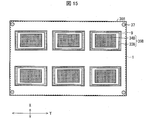
本発明の実施形態3について、図15~図18に基づいて説明する。図15は、本発明の実施形態3に係る基板搭載部30Bの構成を表す平面図である。図16は基板搭載部30Bに搭載された基板における有機EL表示パネル形成領域近傍の断面図である。図17は、基板搭載部30Bに搭載された基板1におけるインク材7a硬化後の有機EL表示パネル形成領域9近傍の断面図である。なお、図16では、矢印に示す方向(紙面右から左への方向)がインクジェットヘッドのスキャン方向(インク材7aの塗布方向)である。
本発明の実施形態3について、図15~図18に基づいて説明する。図15は、本発明の実施形態3に係る基板搭載部30Bの構成を表す平面図である。図16は基板搭載部30Bに搭載された基板における有機EL表示パネル形成領域近傍の断面図である。図17は、基板搭載部30Bに搭載された基板1におけるインク材7a硬化後の有機EL表示パネル形成領域9近傍の断面図である。なお、図16では、矢印に示す方向(紙面右から左への方向)がインクジェットヘッドのスキャン方向(インク材7aの塗布方向)である。
インクジェット塗布装置13(図5)の基板搭載ステージ41と、レベリング装置14(図6)の基板搭載ステージ21との少なくとも一方に、基板搭載部30Bが設けられていてもよい。
図15および図16に示すように、基板搭載部30Bは、温度調整がされマトリクス状に配置された温度調整部39Bを有する。温度調整部39Bは、温度調整がされている低温部34Bおよび高温部33Bを有する。
温度調整部39B間は、基板搭載ステージ41または基板搭載ステージ21を構成する金属材料であるステージ基材30aが配されており、熱源は配置されていない。
高温部33Bは、低温部34Bに囲まれた領域内であって画素形成領域3に対応する位置に配置されており、第2温度に調整されている。高温部33Bは金属板と当該金属板を加熱する熱電素子などの加熱機構を有する。
基板1において画素形成領域3の位置に高温部33Bが接触すると、基板1に塗布されたインク材7aのうち、画素形成領域3を覆う部分に熱が加わることでインク材7aの流動が促進され、インク材7aの平坦化が促進される。これにより、インク材7aの平坦化処理に係る時間を向上させることができる。
低温部34Bは、枠状バンク4に対応する位置に枠状に配置され、第1温度に調整されている。低温部34Bは、空気、水、その他断熱材料から構成することができる。低温部34Bを空気から構成する場合、低温部34Bは基板搭載部30Bの表面(基板1の搭載面)から凹んだ溝とすればよい。
また、低温部34Bは水冷式の断熱機構を有していてもよい、図18は水冷式の低温部34Bの概略構成を表す図である。図18において低温部34Bは、流入管34Baと、循環部34Bbと、排出管34Bcとを備えている、循環部34Bbは、高温部33Bと離間しつつ高温部33Bcを囲っている。流入管34Baおよび排出管34Bcは、循環部34Bbと接続されている。図18の矢印に示すように、流入管34Baから循環部34Bbに流入した水は循環部34Bb内を通り、高温部33Bの周囲を回って、排出管34Bcから排出される。このようにして基板1のうち枠状バンク4近傍を冷却することができる。
これによると、インクジェットヘッド42のノズルから滴下されてインク材7aが基板1に塗布された後、枠状バンク4近傍でのインク材7aの流動を抑制することができる。これにより、インクが枠状バンク4を乗り越えることを抑制することができると共に、図17に示すように、インク材7aが硬化した有機層7のうち、膜厚が異なる部分である縁部7bの幅を狭くすることができる。
そして、図3に示したように、有機層7上に無機層8を形成することで、膜厚が異なる部分である縁部5aの幅が狭い封止層5を形成することができる。これによると、インクジェット法により高品質な封止層5を形成することができる。また、画素形成領域3の周囲の額縁領域の幅が小さい有機EL表示装置を形成することができる。
図15および図16に示すように、基板搭載部30Bにおいて、高温部33Bは、画素形成領域3と重なる位置に配置されている。そして高温部33Bは、雰囲気温度より高い第2温度となっている。
このため、基板1に塗布されたインク材7aのうち、画素形成領域3を覆う部分に熱が加わることで流動が促進され、インク材7aの平坦化が促進される。これにより、インク材7aの平坦化処理に係る時間を短縮させることができる。この結果、図17に示すように、短時間で平坦な有機膜7を形成することができる。
そして、図3に示したように、有機層7上に無機層8を形成することで、平坦な封止層5を形成することができる。
〔実施形態4〕
本発明の実施形態4について、図19に基づいて説明する。図19は、本発明の実施形態4に係る基板搭載部と設定温度とを表す図である。図19の(a)は本発明の実施形態4に係る基板搭載部30Cの構成を表す断面図であり、(b)は(a)に示す基板搭載部30Cにおける第1の温度勾配の例を表す図であり、(c)は(a)に示す基板搭載部30Cの第2の温度勾配の例を表す図である。
本発明の実施形態4について、図19に基づいて説明する。図19は、本発明の実施形態4に係る基板搭載部と設定温度とを表す図である。図19の(a)は本発明の実施形態4に係る基板搭載部30Cの構成を表す断面図であり、(b)は(a)に示す基板搭載部30Cにおける第1の温度勾配の例を表す図であり、(c)は(a)に示す基板搭載部30Cの第2の温度勾配の例を表す図である。
インクジェット塗布装置13(図5)の基板搭載ステージ41と、レベリング装置14(図6)の基板搭載ステージ21との少なくとも一方に、基板搭載部30Cが設けられていてもよい。
基板搭載部30Cは、基板搭載部30(図8、図9)において、高温部33に温度勾配を持たせた構成である。図19の(a)では、矢印に示す方向(紙面左から右へ向かう方向)がインクジェットヘッドのスキャン方向(インク材7aの塗布方向)である。
図19の(a)に示すように、インクジェット塗布装置13(図5)にて塗布されたインク材7aは、塗布された直後は、塗布開始位置7asと、塗布終了位置7aeとで高さが異なる。
例えば、塗布開始位置7asの方が塗布終了位置7aeよりも基板上に滞留する時間が長いため、その滞留によるレベリングの効果から高さが低くなる傾向にある。
ここで、基板搭載部30Cの断面において、高温部33を構成する温度調整素子31のうち、塗布開始位置7asに近い側から塗布終了位置7aeに近い側にかけて、順に、温度調整素子31b、温度調整素子31c、温度調整素子31d、温度調整素子31eとする。また、高温部33を挟む低温部34のうち、温度調整素子31b近傍の温度調整素子を温度調整素子31aとし、温度調整素子31e近傍の温度調整素子を温度調整素子31fとする。
図19の(a)(b)に示すようにすると、高温部33においては、温度調整素子31bから温度調整素子31eにかけて(すなわちインクジェットヘッドのスキャン方向に)温度勾配を有するように、各温度調整素子31の温度を調整する。
この塗布された直後のインク材の高さは、インク材の粘度、インクジェット塗布装置13の塗布するための設定値等による。図19の(b)では、塗布開始位置7as近傍の方が、塗布終了位置7ae近傍の温度よりも高くなるように温度勾配を設けている例を示している。
図19の(a)に示したように、塗布開始位置7asよりも塗布終了位置7aeのインク材7aの高さが高い場合、図19の(b)に示すように、高温部33のうち、塗布開始位置7as近傍の温度tsよりも塗布終了位置7ae近傍の温度teの方が高くなるように、高温部33の温度を調整する。これは、インク材の高さを平坦にするためには高さが高いところのインク材の流動性を上げる必要があるためである。
このように、高温部33を、塗布開始位置7asから塗布終了位置7aeでのインク材7aの高さに応じた温度に温度調整することで、インク材7aのレベリング速度を向上させることができる。
なお、図19の(b)においても、画素形成領域3と対向する高温部33(温度調整素子31b~31e)の温度ts・teは雰囲気温度より大きく、枠状バンク4と対向する低温部34(温度養成素子31a・31f)の温度tbは雰囲気温度以下である。
また、図19の(c)に示すように、高温部33のうち、中央の温度tcを相対的に高くし(例えば、温度調整素子31c・31dの温度を高くし)、縁の部分の温度ts・teを温度tcより低くする(例えば、温度調整素子31b・31fの温度を低くする)ようにしてもよい。
これにより、画素形成領域3の中央近傍のインク材7aを流動させて平坦化することができる。そして、画素形成領域3の縁部分の流動は中央近傍よりも相対的に抑えられて、低温部34近傍のインクの流動を抑えやすくすることができる。このため、より確実に、インク材7aが枠状バンク4を乗り越えることを抑制することができる。
なお、図19の(c)においても、画素形成領域3と対向する高温部33(温度調整素子31b~31e)の温度tc・ts・teは雰囲気温度より大きく、枠状バンク4と対向する低温部34(温度養成素子31a・31f)の温度tbは雰囲気温度以下である。
そして、図19の(a)(b)(c)に示した基板搭載部30Cによっても、図10に示した有機層7と同様に、縁部7bの幅が狭く平坦な有機層7を形成することができる。この結果、図3に示したように縁部5aの幅が狭く平坦な封止層5を形成することができる。
なお、基板搭載部30A・30Bにおいても同様に、高温部33A・33Bを、インク材7aの塗布開始位置7asから塗布終了位置7aeまでの高さに応じて温度勾配を持たせてもよい。
〔まとめ〕
本発明の態様1に係る基板搭載ステージは、有機EL表示パネル形成領域がマトリクス状に配置された基板を搭載する基板搭載ステージであって、上記有機EL表示パネル形成領域には、画素がマトリクス状に配置された画素形成領域と、当該画素形成領域を枠状に囲む枠状バンクと、当該枠状バンク内であって上記画素形成領域を覆うようにインクジェット法により塗布された硬化前のインク材とが配置されており、上記基板搭載ステージは、温度調整がされマトリクス状に配置された温度調整部を有し、上記温度調整部は、上記枠状バンクに対応する位置に枠状に配置され、雰囲気温度以下の第1温度である低温部を有することを特徴とする。
本発明の態様1に係る基板搭載ステージは、有機EL表示パネル形成領域がマトリクス状に配置された基板を搭載する基板搭載ステージであって、上記有機EL表示パネル形成領域には、画素がマトリクス状に配置された画素形成領域と、当該画素形成領域を枠状に囲む枠状バンクと、当該枠状バンク内であって上記画素形成領域を覆うようにインクジェット法により塗布された硬化前のインク材とが配置されており、上記基板搭載ステージは、温度調整がされマトリクス状に配置された温度調整部を有し、上記温度調整部は、上記枠状バンクに対応する位置に枠状に配置され、雰囲気温度以下の第1温度である低温部を有することを特徴とする。
上記構成によると、上記インク材が塗布された後、上記枠状バンク近傍での当該インク材の流動を抑制することができる。これにより、インクが枠状バンクを乗り越えることを抑制し、上記インク材が硬化した後、膜厚が異なる部分である縁部の幅を狭くすることができる。これによると、インクジェット法により高品質な膜を形成することができる。また、画素形成領域の周囲の額縁領域の幅が小さい有機EL表示装置を形成することができる。
本発明の態様2に係る基板搭載ステージは、上記態様1において、上記温度調整部は、上記低温部に囲まれた領域内であって上記画素形成領域に対応する位置に配置され、上記雰囲気温度より高い第2温度である高温部を有していてもよい。
上記構成によると、上記画素形成領域を覆う上記インク材の流動が促進され、上記インク材の平坦化が促進される。これにより、上記インク材の平坦化処理に係る時間を向上させることができる。
本発明の態様3に係る基板搭載ステージは、上記態様2において、マトリクス状に配置され、上記第1温度である温度調整素子を有し、上記低温部は、複数の上記温度調整素子によって構成されていてもよい。
上記構成によると、上記枠状バンクの形状に合わせて、上記低温部を設定することができる。このため、汎用性が高い基板搭載ステージを得ることができる。
本発明の態様4に係る基板搭載ステージは、上記態様2において、マトリクス状に配置され、上記第1温度または上記第2温度である温度調整素子を有し、上記低温部および上記高温部は、それぞれ、複数の上記温度調整素子によって構成されていてもよい。
上記構成によると、上記枠状バンクおよび上記画素形成領域の形状に合わせて、上記低温部および上記高温部を設定することができる。このため、汎用性が高い基板搭載ステージを得ることができる。
本発明の態様5に係る基板搭載ステージは、上記態様3または4において、上記低温部と上記高温部との間には、断熱部が配置されていてもよい。上記構成によると、精度よく、上記低温部を上記第1温度で維持し、上記高温部を上記第2温度で維持させることができる。
本発明の態様6に係る基板搭載ステージは、上記態様5において、上記断熱部は、上記温度調整素子の周囲に格子状に設けられており、流体が流れる循環部を有していてもよい。
本発明の態様7に係る基板搭載ステージは、上記態様5において、上記断熱部は、上記温度調整素子の周囲に格子状に設けられており、上記基板搭載ステージの表面から凹んだ溝形状を有していてもよい。
本発明の態様8に係る基板搭載ステージは、上記態様2、4~7において、上記高温部は、上記インクジェット法による上記インク材の塗布開始位置から塗布終了位置にかけて温度勾配を有するように温度調整されていてもよい。
上記構成によると、上記高温部を、上記塗布開始位置から塗布終了位置での上記インク材の高さに応じた温度に温度調整することが可能である。これにより、上記インク材の平坦化処理に係る時間を向上させることができる。
本発明の態様9に係る基板搭載ステージは、上記態様8において、上記高温部は、上記塗布開始位置よりも、上記画素形成領域の中央の方が、温度が高くてもよい。
本発明の態様10に係る基板搭載ステージは、上記態様8または9において、上記高温部は、上記塗布開始位置および上記塗布終了位置よりも、上記画素形成領域の中央の方が、温度が高くてもよい。
本発明の態様11に係る基板搭載ステージは、上記態様3または4において、上記温度調整素子はペルチェ素子によって構成されていてもよい。
本発明の態様12に係るインクジェット塗布装置は、上記態様1~11における上記基板搭載ステージを有し、上記インク材を塗布してもよい。
本発明の態様13に係るレベリング塗布装置は、上記態様1~11における上記基板搭載ステージを有し、上記インク材を平坦化してもよい。
本発明の態様14に係る有機EL表示装置の製造方法は、有機EL表示パネル形成領域がマトリクス状に配置された基板から有機EL表示装置を製造する有機EL表示装置の製造方法であって、
上記有機EL表示パネル形成領域には、画素がマトリクス状に配置された画素形成領域と、当該画素形成領域を枠状に囲む枠状バンクと、当該枠状バンク内であって上記画素形成領域を覆うようにインクジェット法により塗布された硬化前のインク材とが配置されており、
上記インク材がインクジェット法にて塗布された後、上記基板における上記枠状バンクに対応する位置を、雰囲気温度以下である第1温度に調整する温度調整工程を含むことを特徴とする。
上記有機EL表示パネル形成領域には、画素がマトリクス状に配置された画素形成領域と、当該画素形成領域を枠状に囲む枠状バンクと、当該枠状バンク内であって上記画素形成領域を覆うようにインクジェット法により塗布された硬化前のインク材とが配置されており、
上記インク材がインクジェット法にて塗布された後、上記基板における上記枠状バンクに対応する位置を、雰囲気温度以下である第1温度に調整する温度調整工程を含むことを特徴とする。
本発明の態様15に係る有機EL表示装置の製造方法は、上記態様14において、上記温度調整工程では、さらに、上記基板における上記画素形成領域に対応する位置を、上記雰囲気温度より高い第2温度に調整することが好ましい。
本発明は上述した各実施形態に限定されるものではなく、請求項に示した範囲で種々の変更が可能であり、異なる実施形態にそれぞれ開示された技術的手段を適宜組み合わせて得られる実施形態についても本発明の技術的範囲に含まれる。さらに、各実施形態にそれぞれ開示された技術的手段を組み合わせることにより、新しい技術的特徴を形成することができる。
1 基板
2 TFT基板
3 画素形成領域
4 枠状バンク
5 封止層
5a 縁部
6、8 無機膜
7 有機膜
7a インク材
7ae 塗布終了位置
7as 塗布開始位置
9 有機EL表示パネル形成領域
10 封止システム
11 TFT工程S
12 基板搬送ロボット
12 有機EL工程S
13 インクジェット塗布装置
14 レベリング装置
21・41 基板搭載ステージ
22 UV光源
30・30A~30C 基板搭載部
31 温度調整素子
32 断熱部
33・33A・33B 高温部
34・34B 低温部
37 リフトピン
39・39B 温度調整部
42 インクジェットヘッド
43 ヘッド支持部
2 TFT基板
3 画素形成領域
4 枠状バンク
5 封止層
5a 縁部
6、8 無機膜
7 有機膜
7a インク材
7ae 塗布終了位置
7as 塗布開始位置
9 有機EL表示パネル形成領域
10 封止システム
11 TFT工程S
12 基板搬送ロボット
12 有機EL工程S
13 インクジェット塗布装置
14 レベリング装置
21・41 基板搭載ステージ
22 UV光源
30・30A~30C 基板搭載部
31 温度調整素子
32 断熱部
33・33A・33B 高温部
34・34B 低温部
37 リフトピン
39・39B 温度調整部
42 インクジェットヘッド
43 ヘッド支持部
Claims (15)
- 有機EL表示パネル形成領域がマトリクス状に配置された基板を搭載する基板搭載ステージであって、
上記有機EL表示パネル形成領域には、画素がマトリクス状に配置された画素形成領域と、当該画素形成領域を枠状に囲む枠状バンクと、当該枠状バンク内であって上記画素形成領域を覆うようにインクジェット法により塗布された硬化前のインク材とが配置されており、
上記基板搭載ステージは、温度調整がされマトリクス状に配置された温度調整部を有し、
上記温度調整部は、上記枠状バンクに対応する位置に枠状に配置され、雰囲気温度以下の第1温度である低温部を有することを特徴とする基板搭載ステージ。 - 上記温度調整部は、上記低温部に囲まれた領域内であって上記画素形成領域に対応する位置に配置され、上記雰囲気温度より高い第2温度である高温部を有することを特徴とする請求項1に記載の基板搭載ステージ。
- マトリクス状に配置され、上記第1温度である温度調整素子を有し、
上記低温部は、複数の上記温度調整素子によって構成されていることを特徴とする請求項2に記載の基板搭載ステージ。 - マトリクス状に配置され、上記第1温度または上記第2温度である温度調整素子を有し、
上記低温部および上記高温部は、それぞれ、複数の上記温度調整素子によって構成されていることを特徴とする請求項2に記載の基板搭載ステージ。 - 上記低温部と上記高温部との間には、断熱部が配置されていることを特徴とする請求項3または4に記載の基板搭載ステージ。
- 上記断熱部は、上記温度調整素子の周囲に格子状に設けられており、流体が流れる循環部を有することを特徴とする請求項5に記載の基板搭載ステージ。
- 上記断熱部は、上記温度調整素子の周囲に格子状に設けられており、上記基板搭載ステージの表面から凹んだ溝形状を有することを特徴とする請求項5に記載の基板搭載ステージ。
- 上記高温部は、上記インクジェット法による上記インク材の塗布開始位置から塗布終了位置にかけて温度勾配を有するように温度調整されていることを特徴とする請求項2、4~7の何れか1項に記載の基板搭載ステージ。
- 上記高温部は、上記塗布開始位置よりも、上記画素形成領域の中央の方が、温度が高いことを特徴とする請求項8に記載の基板搭載ステージ。
- 上記高温部は、上記塗布開始位置および上記塗布終了位置よりも、上記画素形成領域の中央の方が、温度が高いことを特徴とする請求項8または9に記載の基板搭載ステージ。
- 上記温度調整素子はペルチェ素子によって構成されていることを特徴とする請求項3または4に記載の基板搭載ステージ。
- 請求項1~11の何れか1項に記載の基板搭載ステージを有し、上記インク材を塗布することを特徴とするインクジェット塗布装置。
- 請求項1~11の何れか1項に記載の基板搭載ステージを有し、上記インク材を平坦化することを特徴とするレベリング装置。
- 有機EL表示パネル形成領域がマトリクス状に配置された基板から有機EL表示装置を製造する有機EL表示装置の製造方法であって、
上記有機EL表示パネル形成領域には、画素がマトリクス状に配置された画素形成領域と、当該画素形成領域を枠状に囲む枠状バンクと、当該枠状バンク内であって上記画素形成領域を覆うようにインクジェット法により塗布された硬化前のインク材とが配置されており、
上記インク材がインクジェット法にて塗布された後、上記基板における上記枠状バンクに対応する位置を、雰囲気温度以下である第1温度に調整する温度調整工程を含むことを特徴とする有機EL表示装置の製造方法。 - 上記温度調整工程では、さらに、上記基板における上記画素形成領域に対応する位置を、上記雰囲気温度より高い第2温度に調整することを特徴とする請求項14に記載の有機EL表示装置の製造方法。
Priority Applications (3)
| Application Number | Priority Date | Filing Date | Title |
|---|---|---|---|
| CN201780087171.4A CN110383952A (zh) | 2017-02-27 | 2017-02-27 | 基板装载台、喷墨涂敷装置、流平装置和有机el显示装置的制造方法 |
| PCT/JP2017/007401 WO2018154764A1 (ja) | 2017-02-27 | 2017-02-27 | 基板搭載ステージ、インクジェット塗布装置、レベリング装置および有機el表示装置の製造方法 |
| US16/064,468 US20190363302A1 (en) | 2017-02-27 | 2017-02-27 | Substrate mounting stage, ink-jet applying device, leveling device, and method for manufacturing organic el display device |
Applications Claiming Priority (1)
| Application Number | Priority Date | Filing Date | Title |
|---|---|---|---|
| PCT/JP2017/007401 WO2018154764A1 (ja) | 2017-02-27 | 2017-02-27 | 基板搭載ステージ、インクジェット塗布装置、レベリング装置および有機el表示装置の製造方法 |
Publications (1)
| Publication Number | Publication Date |
|---|---|
| WO2018154764A1 true WO2018154764A1 (ja) | 2018-08-30 |
Family
ID=63252521
Family Applications (1)
| Application Number | Title | Priority Date | Filing Date |
|---|---|---|---|
| PCT/JP2017/007401 Ceased WO2018154764A1 (ja) | 2017-02-27 | 2017-02-27 | 基板搭載ステージ、インクジェット塗布装置、レベリング装置および有機el表示装置の製造方法 |
Country Status (3)
| Country | Link |
|---|---|
| US (1) | US20190363302A1 (ja) |
| CN (1) | CN110383952A (ja) |
| WO (1) | WO2018154764A1 (ja) |
Citations (4)
| Publication number | Priority date | Publication date | Assignee | Title |
|---|---|---|---|---|
| JP2009039674A (ja) * | 2007-08-10 | 2009-02-26 | Seiko Epson Corp | 成膜方法、及び成膜装置 |
| US20150064825A1 (en) * | 2013-08-27 | 2015-03-05 | Samsung Display Co., Ltd. | Display apparatus manufacturing method |
| JP2015204371A (ja) * | 2014-04-14 | 2015-11-16 | 株式会社石井表記 | 塗布膜形成乾燥装置 |
| JP2016018669A (ja) * | 2014-07-08 | 2016-02-01 | 株式会社Joled | 有機発光デバイスの製造方法 |
Family Cites Families (5)
| Publication number | Priority date | Publication date | Assignee | Title |
|---|---|---|---|---|
| JP4440523B2 (ja) * | 2002-09-19 | 2010-03-24 | 大日本印刷株式会社 | インクジェット法による有機el表示装置及びカラーフィルターの製造方法、製造装置 |
| US6908045B2 (en) * | 2003-01-28 | 2005-06-21 | Casio Computer Co., Ltd. | Solution spray apparatus and solution spray method |
| US7584701B2 (en) * | 2004-12-30 | 2009-09-08 | E.I. Du Pont De Nemours And Company | Processes for printing layers for electronic devices and printing apparatuses for performing the processes |
| JP4251329B2 (ja) * | 2005-12-20 | 2009-04-08 | カシオ計算機株式会社 | 表示装置及びその製造方法 |
| KR102163521B1 (ko) * | 2013-05-15 | 2020-10-12 | 삼성디스플레이 주식회사 | 유기 발광 표시 장치의 제조 장치 및 유기 발광 표시 장치의 제조 방법 |
-
2017
- 2017-02-27 US US16/064,468 patent/US20190363302A1/en not_active Abandoned
- 2017-02-27 WO PCT/JP2017/007401 patent/WO2018154764A1/ja not_active Ceased
- 2017-02-27 CN CN201780087171.4A patent/CN110383952A/zh active Pending
Patent Citations (4)
| Publication number | Priority date | Publication date | Assignee | Title |
|---|---|---|---|---|
| JP2009039674A (ja) * | 2007-08-10 | 2009-02-26 | Seiko Epson Corp | 成膜方法、及び成膜装置 |
| US20150064825A1 (en) * | 2013-08-27 | 2015-03-05 | Samsung Display Co., Ltd. | Display apparatus manufacturing method |
| JP2015204371A (ja) * | 2014-04-14 | 2015-11-16 | 株式会社石井表記 | 塗布膜形成乾燥装置 |
| JP2016018669A (ja) * | 2014-07-08 | 2016-02-01 | 株式会社Joled | 有機発光デバイスの製造方法 |
Also Published As
| Publication number | Publication date |
|---|---|
| CN110383952A (zh) | 2019-10-25 |
| US20190363302A1 (en) | 2019-11-28 |
Similar Documents
| Publication | Publication Date | Title |
|---|---|---|
| KR100510003B1 (ko) | 표시용 패널의 제조 방법 | |
| CN101681570A (zh) | 显示元件的制造方法、显示元件的制造装置及显示元件 | |
| JP6591629B2 (ja) | 樹脂フィルムの剥離方法及び装置、電子デバイスの製造方法並びに有機el表示装置の製造方法 | |
| TWI444968B (zh) | Surface light display device | |
| CN101983397A (zh) | 面发光显示装置 | |
| US7282385B2 (en) | Electro-optical device, method of manufacturing electro-optical device, and electronic apparatus | |
| CN107409455A (zh) | 薄膜元件装置的制造方法及其所使用的光照射装置 | |
| JPWO2017010329A1 (ja) | エレクトロルミネッセンス装置 | |
| US6890782B2 (en) | Manufacturing method of electroluminescence display apparatus | |
| JP4630535B2 (ja) | 表示装置の製造方法 | |
| US20170120501A1 (en) | Apparatus and method for manufacturing display apparatus | |
| US20200144303A1 (en) | Thin film transistor substrate and method for producing thin film transistor substrate | |
| US20110290414A1 (en) | Method for manufacturing color electrophoretic display device | |
| JP2017152226A (ja) | 表示装置およびその製造方法 | |
| WO2018154764A1 (ja) | 基板搭載ステージ、インクジェット塗布装置、レベリング装置および有機el表示装置の製造方法 | |
| JP2015201256A (ja) | 有機エレクトロルミネッセンス装置の製造方法および電子機器 | |
| KR101374015B1 (ko) | 합착 장치 및 이를 사용한 유기발광표시장치의 제조 방법 | |
| KR100671197B1 (ko) | 평판표시장치와 이의 제조방법 | |
| US9972781B2 (en) | Method of manufacturing mask and method of manufacturing display device | |
| TW201924107A (zh) | 有機電致發光器件及光列印頭 | |
| CN109546011B (zh) | 膜层的制作方法、显示基板及其制作方法与设备 | |
| US20190360091A1 (en) | Vapor deposition mask, vapor deposition apparatus, and method for producing display device | |
| US10732462B2 (en) | Display device, and method of producing display device | |
| KR20250170157A (ko) | 표시 장치의 제조 방법 및 표시 장치의 제조 방법에 따라 제조된 표시 장치 | |
| US20250281941A1 (en) | Apparatus for fabricating display panel |
Legal Events
| Date | Code | Title | Description |
|---|---|---|---|
| 121 | Ep: the epo has been informed by wipo that ep was designated in this application |
Ref document number: 17897558 Country of ref document: EP Kind code of ref document: A1 |
|
| NENP | Non-entry into the national phase |
Ref country code: DE |
|
| 122 | Ep: pct application non-entry in european phase |
Ref document number: 17897558 Country of ref document: EP Kind code of ref document: A1 |
|
| NENP | Non-entry into the national phase |
Ref country code: JP |