WO2018147274A1 - Image display device - Google Patents
Image display device Download PDFInfo
- Publication number
- WO2018147274A1 WO2018147274A1 PCT/JP2018/004005 JP2018004005W WO2018147274A1 WO 2018147274 A1 WO2018147274 A1 WO 2018147274A1 JP 2018004005 W JP2018004005 W JP 2018004005W WO 2018147274 A1 WO2018147274 A1 WO 2018147274A1
- Authority
- WO
- WIPO (PCT)
- Prior art keywords
- pattern
- section
- image display
- light
- sections
- Prior art date
Links
Images


Classifications
-
- G—PHYSICS
- G02—OPTICS
- G02F—OPTICAL DEVICES OR ARRANGEMENTS FOR THE CONTROL OF LIGHT BY MODIFICATION OF THE OPTICAL PROPERTIES OF THE MEDIA OF THE ELEMENTS INVOLVED THEREIN; NON-LINEAR OPTICS; FREQUENCY-CHANGING OF LIGHT; OPTICAL LOGIC ELEMENTS; OPTICAL ANALOGUE/DIGITAL CONVERTERS
- G02F1/00—Devices or arrangements for the control of the intensity, colour, phase, polarisation or direction of light arriving from an independent light source, e.g. switching, gating or modulating; Non-linear optics
- G02F1/01—Devices or arrangements for the control of the intensity, colour, phase, polarisation or direction of light arriving from an independent light source, e.g. switching, gating or modulating; Non-linear optics for the control of the intensity, phase, polarisation or colour
- G02F1/13—Devices or arrangements for the control of the intensity, colour, phase, polarisation or direction of light arriving from an independent light source, e.g. switching, gating or modulating; Non-linear optics for the control of the intensity, phase, polarisation or colour based on liquid crystals, e.g. single liquid crystal display cells
- G02F1/133—Constructional arrangements; Operation of liquid crystal cells; Circuit arrangements
- G02F1/1333—Constructional arrangements; Manufacturing methods
- G02F1/1335—Structural association of cells with optical devices, e.g. polarisers or reflectors
- G02F1/1336—Illuminating devices
- G02F1/133602—Direct backlight
- G02F1/133611—Direct backlight including means for improving the brightness uniformity
-
- F—MECHANICAL ENGINEERING; LIGHTING; HEATING; WEAPONS; BLASTING
- F21—LIGHTING
- F21S—NON-PORTABLE LIGHTING DEVICES; SYSTEMS THEREOF; VEHICLE LIGHTING DEVICES SPECIALLY ADAPTED FOR VEHICLE EXTERIORS
- F21S2/00—Systems of lighting devices, not provided for in main groups F21S4/00 - F21S10/00 or F21S19/00, e.g. of modular construction
-
- G—PHYSICS
- G02—OPTICS
- G02F—OPTICAL DEVICES OR ARRANGEMENTS FOR THE CONTROL OF LIGHT BY MODIFICATION OF THE OPTICAL PROPERTIES OF THE MEDIA OF THE ELEMENTS INVOLVED THEREIN; NON-LINEAR OPTICS; FREQUENCY-CHANGING OF LIGHT; OPTICAL LOGIC ELEMENTS; OPTICAL ANALOGUE/DIGITAL CONVERTERS
- G02F1/00—Devices or arrangements for the control of the intensity, colour, phase, polarisation or direction of light arriving from an independent light source, e.g. switching, gating or modulating; Non-linear optics
- G02F1/01—Devices or arrangements for the control of the intensity, colour, phase, polarisation or direction of light arriving from an independent light source, e.g. switching, gating or modulating; Non-linear optics for the control of the intensity, phase, polarisation or colour
- G02F1/13—Devices or arrangements for the control of the intensity, colour, phase, polarisation or direction of light arriving from an independent light source, e.g. switching, gating or modulating; Non-linear optics for the control of the intensity, phase, polarisation or colour based on liquid crystals, e.g. single liquid crystal display cells
- G02F1/133—Constructional arrangements; Operation of liquid crystal cells; Circuit arrangements
- G02F1/1333—Constructional arrangements; Manufacturing methods
- G02F1/1335—Structural association of cells with optical devices, e.g. polarisers or reflectors
- G02F1/1336—Illuminating devices
- G02F1/133602—Direct backlight
- G02F1/133605—Direct backlight including specially adapted reflectors
-
- G—PHYSICS
- G02—OPTICS
- G02F—OPTICAL DEVICES OR ARRANGEMENTS FOR THE CONTROL OF LIGHT BY MODIFICATION OF THE OPTICAL PROPERTIES OF THE MEDIA OF THE ELEMENTS INVOLVED THEREIN; NON-LINEAR OPTICS; FREQUENCY-CHANGING OF LIGHT; OPTICAL LOGIC ELEMENTS; OPTICAL ANALOGUE/DIGITAL CONVERTERS
- G02F1/00—Devices or arrangements for the control of the intensity, colour, phase, polarisation or direction of light arriving from an independent light source, e.g. switching, gating or modulating; Non-linear optics
- G02F1/01—Devices or arrangements for the control of the intensity, colour, phase, polarisation or direction of light arriving from an independent light source, e.g. switching, gating or modulating; Non-linear optics for the control of the intensity, phase, polarisation or colour
- G02F1/13—Devices or arrangements for the control of the intensity, colour, phase, polarisation or direction of light arriving from an independent light source, e.g. switching, gating or modulating; Non-linear optics for the control of the intensity, phase, polarisation or colour based on liquid crystals, e.g. single liquid crystal display cells
- G02F1/133—Constructional arrangements; Operation of liquid crystal cells; Circuit arrangements
- G02F1/1333—Constructional arrangements; Manufacturing methods
- G02F1/1335—Structural association of cells with optical devices, e.g. polarisers or reflectors
- G02F1/1336—Illuminating devices
- G02F1/133602—Direct backlight
- G02F1/133608—Direct backlight including particular frames or supporting means
-
- G—PHYSICS
- G09—EDUCATION; CRYPTOGRAPHY; DISPLAY; ADVERTISING; SEALS
- G09F—DISPLAYING; ADVERTISING; SIGNS; LABELS OR NAME-PLATES; SEALS
- G09F9/00—Indicating arrangements for variable information in which the information is built-up on a support by selection or combination of individual elements
-
- G—PHYSICS
- G02—OPTICS
- G02F—OPTICAL DEVICES OR ARRANGEMENTS FOR THE CONTROL OF LIGHT BY MODIFICATION OF THE OPTICAL PROPERTIES OF THE MEDIA OF THE ELEMENTS INVOLVED THEREIN; NON-LINEAR OPTICS; FREQUENCY-CHANGING OF LIGHT; OPTICAL LOGIC ELEMENTS; OPTICAL ANALOGUE/DIGITAL CONVERTERS
- G02F1/00—Devices or arrangements for the control of the intensity, colour, phase, polarisation or direction of light arriving from an independent light source, e.g. switching, gating or modulating; Non-linear optics
- G02F1/01—Devices or arrangements for the control of the intensity, colour, phase, polarisation or direction of light arriving from an independent light source, e.g. switching, gating or modulating; Non-linear optics for the control of the intensity, phase, polarisation or colour
- G02F1/13—Devices or arrangements for the control of the intensity, colour, phase, polarisation or direction of light arriving from an independent light source, e.g. switching, gating or modulating; Non-linear optics for the control of the intensity, phase, polarisation or colour based on liquid crystals, e.g. single liquid crystal display cells
- G02F1/133—Constructional arrangements; Operation of liquid crystal cells; Circuit arrangements
- G02F1/1333—Constructional arrangements; Manufacturing methods
- G02F1/1335—Structural association of cells with optical devices, e.g. polarisers or reflectors
- G02F1/1336—Illuminating devices
- G02F1/133602—Direct backlight
- G02F1/133603—Direct backlight with LEDs
-
- G—PHYSICS
- G02—OPTICS
- G02F—OPTICAL DEVICES OR ARRANGEMENTS FOR THE CONTROL OF LIGHT BY MODIFICATION OF THE OPTICAL PROPERTIES OF THE MEDIA OF THE ELEMENTS INVOLVED THEREIN; NON-LINEAR OPTICS; FREQUENCY-CHANGING OF LIGHT; OPTICAL LOGIC ELEMENTS; OPTICAL ANALOGUE/DIGITAL CONVERTERS
- G02F1/00—Devices or arrangements for the control of the intensity, colour, phase, polarisation or direction of light arriving from an independent light source, e.g. switching, gating or modulating; Non-linear optics
- G02F1/01—Devices or arrangements for the control of the intensity, colour, phase, polarisation or direction of light arriving from an independent light source, e.g. switching, gating or modulating; Non-linear optics for the control of the intensity, phase, polarisation or colour
- G02F1/13—Devices or arrangements for the control of the intensity, colour, phase, polarisation or direction of light arriving from an independent light source, e.g. switching, gating or modulating; Non-linear optics for the control of the intensity, phase, polarisation or colour based on liquid crystals, e.g. single liquid crystal display cells
- G02F1/133—Constructional arrangements; Operation of liquid crystal cells; Circuit arrangements
- G02F1/1333—Constructional arrangements; Manufacturing methods
- G02F1/1335—Structural association of cells with optical devices, e.g. polarisers or reflectors
- G02F1/1336—Illuminating devices
- G02F1/133602—Direct backlight
- G02F1/133606—Direct backlight including a specially adapted diffusing, scattering or light controlling members
-
- G—PHYSICS
- G02—OPTICS
- G02F—OPTICAL DEVICES OR ARRANGEMENTS FOR THE CONTROL OF LIGHT BY MODIFICATION OF THE OPTICAL PROPERTIES OF THE MEDIA OF THE ELEMENTS INVOLVED THEREIN; NON-LINEAR OPTICS; FREQUENCY-CHANGING OF LIGHT; OPTICAL LOGIC ELEMENTS; OPTICAL ANALOGUE/DIGITAL CONVERTERS
- G02F1/00—Devices or arrangements for the control of the intensity, colour, phase, polarisation or direction of light arriving from an independent light source, e.g. switching, gating or modulating; Non-linear optics
- G02F1/01—Devices or arrangements for the control of the intensity, colour, phase, polarisation or direction of light arriving from an independent light source, e.g. switching, gating or modulating; Non-linear optics for the control of the intensity, phase, polarisation or colour
- G02F1/13—Devices or arrangements for the control of the intensity, colour, phase, polarisation or direction of light arriving from an independent light source, e.g. switching, gating or modulating; Non-linear optics for the control of the intensity, phase, polarisation or colour based on liquid crystals, e.g. single liquid crystal display cells
- G02F1/133—Constructional arrangements; Operation of liquid crystal cells; Circuit arrangements
- G02F1/1333—Constructional arrangements; Manufacturing methods
- G02F1/1335—Structural association of cells with optical devices, e.g. polarisers or reflectors
- G02F1/1336—Illuminating devices
- G02F1/133602—Direct backlight
- G02F1/133612—Electrical details
Definitions
- the present disclosure relates to an image display device including a display panel such as a liquid crystal cell.
- Patent Document 1 discloses a display device that uses a surface light source unit including a light-transmitting / reflecting plate for obtaining uniform surface illumination light with less luminance unevenness as a direct backlight.
- the present disclosure provides an image display device capable of displaying with higher uniformity of luminance over the entire screen.
- An image display device includes a display panel, a lower frame including a flat portion having a substantially flat surface facing an effective area of the display panel, a plurality of light sources arranged at substantially equal intervals on the flat portion, A plurality of pillar-shaped support pins arranged at substantially equal intervals in the section are provided with a sheet-like luminance uniform plate supported away from the plurality of light sources, and the luminance uniform plate displays the emitted light of the plurality of light sources.
- the predetermined pattern includes a first pattern that is applied to at least a part of the outer partition that touches the outer periphery of the array, and a partition in which the first pattern is not applied among the plurality of partitions. Less It is also applied to a part, and a different second pattern from the first pattern.
- the image display device of the present disclosure it is possible to display with higher luminance uniformity over the entire screen.
- FIG. 1 is an external perspective view of a liquid crystal television according to an embodiment.
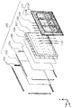
- FIG. 2 is an exploded perspective view of the liquid crystal module according to the embodiment.
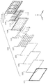
- FIG. 3 is an exploded perspective view of the liquid crystal module according to the embodiment.
- FIG. 4 is a schematic cross-sectional view for explaining a mounting state of support pins in the liquid crystal module.
- FIG. 5 is a schematic cross-sectional view for explaining an example of the configuration of the liquid crystal module.
- FIG. 6 is a schematic diagram showing an example of the opening in the outer compartment located at the corner when the first pattern is applied to all the outer compartments in the liquid crystal module.
- FIG. 7 is a partial cross-sectional view schematically showing a part of the cross section of the liquid crystal module as viewed from the bottom surface direction.
- FIG. 8A is a schematic partial cross-sectional view of a liquid crystal module for explaining a configuration of a uniform luminance plate in a modification of the embodiment.
- FIG. 8B is a schematic partial cross-sectional view of a liquid crystal module for explaining a configuration of a uniform luminance plate in a modification of the embodiment.
- the inventor of the present application has found that the following problems occur with respect to a conventional image display device.
- a display module including a display panel is roughly a thin rectangular parallelepiped on the front and back, but more strictly, the four sides on the back side are relatively large and chamfered. It has such a shape. By adopting such a shape with a small thickness at the end face, an appearance effect is obtained that makes the display module itself appear thin.
- the thickness in the peripheral portion is smaller than the thickness in other portions.
- a display mechanism common to other parts cannot be adopted in the peripheral part of the display panel due to the limitation of the thickness direction of the internal space. Therefore, there is a problem that it is difficult to obtain uniform image quality over the entire screen.
- a section illuminated mainly by a light source on the outermost side of a display panel among a plurality of light sources differs from the other sections in incident light. Has a small amount of light because it includes reflected light from a surface oblique to the incident surface. Further, there is no adjacent section illuminated by the light source in the direction of the edge of the display panel.
- the brightness near the edge of the display panel is as high as other parts. Is difficult to get. That is, luminance unevenness that becomes darker toward the end portion occurs near the end portion of the screen.
- the same luminance unevenness may occur even in a display module having a shape close to a thin rectangular parallelepiped instead of a shape that exhibits the effect of making it look thin as described above.
- it is suppressed to some extent by devising the shape of the lower frame or printing on a reflection sheet or a diffusion plate.
- the lower frame since the lower frame has a shape restriction to make the display module appear thin, the difference in the amount of light entering from the adjacent sections between the sections in the display panel is complicated, and the reflection sheet or the like It is difficult to suppress luminance unevenness due to printing.
- the present disclosure has been made on the basis of such knowledge, and the inventor of the present application has obtained an idea of the structure of an image display device capable of displaying with higher luminance uniformity over the entire screen.
- the vertical direction of the image display device is matched with the y-axis direction
- the front-rear direction is matched with the z-axis direction
- the horizontal direction is matched with the x-axis direction.
- FIG. 1 is an external perspective view of an image display apparatus 10 according to each embodiment.
- 2 and 3 are exploded perspective views of the liquid crystal module 100 according to each embodiment.
- the image display device 10 is, for example, a liquid crystal television, and includes a liquid crystal module 100, a bezel 101, a back cover 103, and a stand 200 as shown in FIG.
- the liquid crystal module 100 is a module for displaying images that can display still images and moving images, and includes a display panel 102.
- the display panel 102 is a so-called liquid crystal cell, and is an element in which liquid crystal is sealed between a plurality of glass plates.
- the display panel 102 is controlled based on the video signal input to the image display device 10 and displays a video.
- the liquid crystal module 100 can be set on a floor or a stand using the stand 200.
- the usage mode of the liquid crystal module 100 is not limited to this.
- the liquid crystal module 100 can be used as the image display device 10 by being hung on a wall or embedded using another fixture, or suspended from the ceiling without using the stand 200. May be.
- the bezel 101 made of resin is divided and formed so as to correspond to each of the four sides of the image display device 10, and is coupled to each other using, for example, screws.
- the bezel 101 sandwiches a plurality of components from a display panel 102 (described later) to a lower frame 111 together with the back cover 103.
- the liquid crystal module 100 having the above configuration further includes a mold frame 104, an optical sheet unit 105, a diffusion plate 106, a luminance uniform plate 107, a reflection sheet 108, and an LED sheet. 109, a relay sheet 110, a lower frame 111, and support pins 112.
- the mold frame 104 supports a plurality of components (so-called backlight units) from the optical sheet unit 105 to the LED sheet 109 and the relay sheet 110 with the lower frame 111 interposed therebetween. In FIG. 3, the mold frame 104 is not shown.
- the optical sheet unit 105 is configured by stacking a plurality of two or three types of sheets having different optical characteristics.
- the optical sheet unit 105 includes a vertical prism sheet, a horizontal prism sheet, and a diffusion sheet.
- the diffusion plate 106 diffuses light incident from a plurality of LEDs (Light-Emitting Diodes) 113 disposed on the LED sheet 109 and serving as a light source of the image display device 10, and emits the light toward the display panel 102.
- LEDs Light-Emitting Diodes
- the luminance uniform plate 107 is a side on which the diffuser 106 and the display panel 102 are provided by increasing the uniformity of the luminance of the light from the plurality of LEDs 113 arranged on the LED sheet 109 (hereinafter also referred to as outgoing light), which varies depending on the location. Make it transparent.
- the uniform brightness plate 107 is a sheet-like member made of a resin such as PET (polyethylene terephthalate) that contains fine bubbles densely and has good light reflectivity.
- the luminance uniform plate 107 has a large number of through-holes formed over substantially the whole. A part of the light emitted from the LED 113 passes through these through holes to the opposite side, that is, the side where the display panel 102 and the diffusion plate 106 are present (in the present disclosure, it is also expressed as “light passes through the luminance uniform plate 107”). is doing).
- the number, size, or distribution of these through holes are adjusted so that the transmission amount per unit area of light from a light source located at a predetermined position apart from each other can be made uniform. That is, all the through holes provided in the luminance uniform plate 107 are not uniformly sized or evenly distributed.
- Such through-holes are arranged in a predetermined pattern applied to each of a plurality of sections that are arranged on the luminance uniform plate 107 and that face each of the LEDs 113.
- the uniform luminance plate 107 is manufactured by, for example, opening through holes arranged in such a pattern using a mold in the resin sheet having a predetermined size.
- the grids on the uniform luminance plate 107 in FIGS. 2 and 3 indicate that there are a plurality of such sections.
- the line dividing the uniform brightness plate 107 into these cells is a virtual line, and such a line is not actually drawn. The same applies to the following drawings.
- the predetermined pattern will be described later in the embodiment.
- the alignment characteristic (hereinafter also referred to as light distribution characteristic) of the light emitted from the LED 113 is smoothed.
- the light from the LED 113 whose light distribution characteristics have been smoothed by the uniform luminance plate 107 is diffused by the diffusion plate 106 so that the luminance unevenness is further suppressed and then emitted toward the display panel 102.
- the reflection sheet 108 is a sheet in which holes having positions and sizes corresponding to the plurality of LEDs 113 arranged on the LED sheet 109 are provided, and reflects light on the entire front surface of the image display device 10. .
- the reflection sheet 108 faces the effective area of the display panel 102, rises from a flat portion having a substantially flat surface smaller than the effective area, and ends of the four sides of the flat portion, and is viewed from the front side of the image display device 10. And a side wall portion that reaches the outer edge of the effective area of the display panel 102, and has a shape that generally follows the lower frame 111 described later.
- the LED sheet 109 is a flexible printed circuit board (hereinafter referred to as FPC (Flexible Printed Circuits)) on which a plurality of LEDs 113 are arranged.
- the LED 113 is disposed on one of the two main surfaces of the sheet-like FPC, and a reflective layer that reflects light is disposed on the main surface on which the FPC LED is disposed, that is, the main surface on the front side of the image display device 10. It is formed.
- the plurality of LEDs 113 on the main surface of the LED sheet 109 are arranged at substantially equal intervals, for example, in a matrix form so that a wide range on the back surface of the display panel 102 can be irradiated with as little unevenness as possible.
- the relay sheet 110 is an FPC in which an electrical path for sending electric power, a control signal, and the like to each LED 113 arranged on the LED sheet 109 is formed. Further, in the relay sheet 110, similarly to the LED sheet 109, a reflective layer is formed on the main surface on the front side of the image display device 10.
- the lower frame 111 is a plate-like member formed of a thin sheet metal and is also referred to as a base plate, and supports the LED sheet 109 and the relay sheet 110.
- the lower frame 111 opposes the effective area of the display panel 102 and rises from a flat portion 111A having a substantially flat surface smaller than the effective area, and from the outer edge of the flat portion 111A, that is, from the ends of the four sides. And a side wall portion 111 ⁇ / b> B reaching the outer edge of the effective area of the display panel 102 when viewed from the front side (side with the display panel 102).
- the liquid crystal module 100 By forming the back cover 103 along the outer shape of the lower frame 111, the liquid crystal module 100 has a shape in which the four sides on the back side are greatly chamfered from the thin rectangular parallelepiped in the front-rear direction (the direction along the z axis). It has the effect of appearance that looks thinner.
- the configurations described in the following embodiments also provide luminance uniformity over the entire effective area of the display panel 102 in a liquid crystal module including a lower frame and a reflective sheet that do not exhibit the above effects. Note that it can be applied to enhance.
- a plurality of LEDs 113 as light sources are arranged on the flat portion 111A of the lower frame 111. More specifically, the LED sheet 109 and the relay sheet 110 in which the plurality of LEDs 113 are arranged at substantially equal intervals are attached to the flat portion 111A. Thereafter, the reflection sheet 108 is further attached so that each LED 113 is exposed from the plurality of holes of the reflection sheet 108. The light emitted from each LED 113 is reflected directly or by the reflection layer and the reflection sheet 108 formed on the FPC, and is incident on the luminance uniform plate 107 on the front side of the image display device 10 with respect to each LED 113.
- the lower frame 111 further supports the backlight unit from the optical sheet unit 105 to the LED sheet 109 and the relay sheet 110 with the mold frame 104 interposed therebetween.
- the lower frame 111 may further have a structure for supporting each structure of the backlight unit.
- the lower frame 111 may have a cut-and-raised part that hangs the optical sheet unit 105 in the vicinity of the upper side when the image display device 10 is put into use.
- the optical sheet unit 105 is provided with, for example, a tab having a hole for hooking it.
- the plurality of support pins 112 shown in FIG. 3 are columnar members.
- Each support pin 112 has a tip end portion 112A which is an end portion on the opposite side to the end portion attached to the lower frame 111, and a flange-like flange portion 112B in the middle of the columnar shape in the longitudinal direction.
- the plurality of support pins 112 are attached to the flat portion 111A of the lower frame 111 through the reflection sheet 108, and support the reflection sheet 108 with the lower frame 111 interposed therebetween.
- FIG. 4 is a schematic diagram for explaining how the support pins 112 attached to the lower frame 111 support the diffusion plate 106 and the luminance uniform plate 107 inside the liquid crystal module 100.
- the configuration of the liquid crystal module 100 that is not necessary for this description is omitted.
- the brightness uniform plate 107 is provided with holes for inserting the support pins 112 at positions corresponding to the plurality of support pins 112 attached to the lower frame 111.
- the brightness uniform plate 107 is attached so that the support pin 112 is inserted into the hole from the tip end portion 112A and supported by the flange portion 112B of the support pin 112 as shown in FIG.
- the support pin 112 may support the luminance uniform plate 107 at a position determined from the design and spaced from the LED 113 on the lower frame 111, and the configuration for this support is limited to the flange-shaped flange portion 112B.
- the support pin 112 may have a base-like portion with a top surface instead of the flange portion 112B, and the luminance uniform plate 107 may be supported by the top surface of this portion.
- the support pin 112 has a portion that becomes thicker from the front to the back of the liquid crystal module 100 when attached, and supports the luminance uniform plate 107 at a place where the diameter of the hole of the luminance uniform plate 107 coincides with this portion. Also good.
- the diffusion plate 106 is supported by the end of the side wall 111B of the lower frame 111 in the periphery, and is erected on the flat portion 111A of the lower frame 111 as shown in FIG. It is supported by the tip 112A of the support pin 112.
- Such support pins 112 are arranged at substantially equal intervals, for example, in a matrix form so as to support the entire diffuser plate 106 and luminance uniform plate 107 in the flat portion 111A. Further, the support pin 112 is arranged at a position away from each LED 113, for example, on a straight line connecting two equidistant points from the two LEDs 113 adjacent in the matrix direction so as not to block the light toward the luminance uniform plate 107 as much as possible.
- the configuration of the liquid crystal module 100 for further improving the uniformity of luminance over the entire screen will be described below.
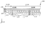
- FIG. 5 is a schematic diagram for explaining the configuration of the liquid crystal module 100 according to the embodiment using an example.
- (a) is an enlarged front view of three sections among a plurality of sections of the uniform brightness plate 107.
- FIG. B is a schematic front view of the entire luminance uniform plate 107. As described above, the boundaries of the grid-like sections that are arranged on the luminance uniform plate 107 are indicated by virtual lines.
- the arrow extending from (b) to (a) indicates the correspondence between the position in the overall view shown in (b) and the position in the enlarged view shown in (a).
- (A) and a plurality of broken rectangles in (b) indicate the positions of the LEDs 113 arranged on the flat portion 111A in a front view. Each section faces one of the LEDs 113 arranged on the flat portion 111A of the lower frame 111.
- (C) is the figure which looked at the cross section parallel to xz plane of the liquid crystal module 100 from the bottom face direction.
- the two dotted lines extending over (b) and (c) indicate positions corresponding to the boundary between the flat portion 111A and the side wall portion 111B of the lower frame 111. This position is indicated by a dotted line having the same appearance in the enlarged view of (a).
- Each of the plurality of circles in FIG. 5A indicates an opening of a through hole formed in the luminance uniform plate 107.
- the openings 107h, 107i, 107j, and 107k are through-hole openings used for examples in the following description. Common reference numerals are assigned to openings of the same size. In addition, in (b), illustration of the opening part of these through-holes is abbreviate
- the through holes are arranged in a predetermined pattern applied to each section.
- the predetermined pattern used in one luminance uniform plate 107 includes a plurality of patterns.
- the pattern applied to each division changes with the position of the said division in the arrangement
- each section included in the left and right columns is referred to as a section 107B, and each section included in a column between them is referred to as a section 107A. That is, the three sections shown in (a) are arranged in the order of section 107B, section 107A, and section 107B from left to right.
- the section 107B is an example of an outer section described later in the present embodiment.
- the opening area farther from the facing LED 113 generally has a larger opening area.
- both of the opening 107h and the opening 107i are larger than the opening of the through hole closer to the LED 113 at the position overlapping the center of the section 107A. Further, when comparing the opening 107h and the opening 107i, the opening 107h of the through hole farther from the LED 113 is larger.
- the light transmittance changes according to the opening area per unit area (hereinafter referred to as the opening ratio).
- the unit area here can be determined to be smaller than the entire area of one section and larger than the maximum opening area of one through hole.
- the transmittance of the emitted light in the section 107A is adjusted to be lower at a location closer to the LED 113 and higher at a location farther away.
- the brightness of the light transmitted through the brightness uniform plate 107 to the display panel 102 side in the partition 107B can be made to be close to a spatially uniform state.
- the opening area is generally larger as the through hole is farther from the facing LED 113.
- the opening 107h of the through hole farther from the LED 113 is larger.
- the opening 107j of the through hole farther from the LED 113 is larger.
- the through hole closer to the outer periphery of the array of sections has a larger opening area than the through hole located farther from the outer periphery even if the distance from the LED 113 is the same. For example, when comparing the opening 107h and the opening 107j, the opening 107j of the through hole farther from the LED 113 is larger. Similarly, when comparing the opening 107i and the opening 107k, the opening 107k of the through hole farther from the LED 113 is larger.
- Such a difference in the area of the opening of the through hole is provided in common to the right and left sections 107B of the luminance uniform plate 107.
- the transmittance of the emitted light in the section 107B is adjusted to be lower at a location closer to the LED 113 and higher at a location farther away, and the brightness of the light transmitted to the display panel 102 side is spatially uniform. Can be close to the state.
- the brightness of the light transmitted through the brightness uniform plate 107 to the display panel 102 side in the section 107B can be brought close to a spatially uniform state.
- arranging a plurality of through holes having different opening areas in one section is an example of arranging the through holes for changing the opening ratio in the section.
- Other examples of the arrangement of the through holes that change the aperture ratio include an arrangement that changes the density of the through holes having the same opening area (distance between the centers of the openings) within the compartment, and both the opening area and the density of the through holes.
- the shape of the opening is not limited to the circular shape as shown in FIG. 5, and may be a slit shape or any other shape such as a polygon.
- the aperture ratio of the luminance uniform plate 107 by the plurality of through holes and the distance from the LED 113 facing the section 107A Has a positive correlation.
- this pattern is also referred to as a second pattern.
- the aperture ratio of the luminance uniform plate 107 by a plurality of through holes and the distance from the LED 113 facing the section 107B have a positive correlation, and the aperture ratio. And the distance from the outer circumference of the array of sections have a negative correlation.
- this pattern is also referred to as a first pattern.
- the first pattern and the second pattern related to the arrangement of the through holes have been described using a part of a plurality of sections arranged on the luminance uniform plate 107 as an example.
- the position or range of the section to which each pattern is applied in this arrangement will be described.
- the luminance uniform plate 107 forms a rectangular array in which a plurality of sections are arranged in a matrix of 3 rows or more and 3 columns or more.
- the first pattern is applied to at least a part of the outer section that is a section in contact with the outer periphery of the array among the plurality of sections.
- the first pattern may be applied to all the sections 107B included in the left and right columns of the array.
- the second pattern may be applied to all sections to which the first pattern is not applied, that is, all of the sections 107A shown in FIG.
- the luminance uniform plate 107 is used by using a mold capable of punching one or more rows. In the step of sequentially feeding the resin-made sheet in the direction along the short side (y-axis direction), it can be manufactured without reducing the efficiency as compared with the conventional case.
- the first pattern may be applied to all the sections included in the top row and the bottom row of the array.
- the sections included in these rows are also outer sections.
- the first pattern is applied to all the sections included in the top row and the lower row of the array
- the second pattern is applied to the sections included in all the rows between these rows, for example, 1
- a mold that can be perforated in units of rows or more, it is a process of feeding the resin sheet that is the basis of the uniform brightness plate 107 in the direction along the long side (x-axis direction), which is more efficient than conventional Can be manufactured without dropping.
- the section to which the first pattern described so far is applied is an outer section in contact with one of a pair of opposing sides on the outer periphery of the rectangular array.
- the first pattern is also applied to the outer section that touches one of the four sides of the rectangle, that is, the first pattern is applied to all outer sections, and the second pattern is applied to all inner sections that are not touching the outer periphery of the array. May be.
- FIG. 6 shows an opening of the through hole in the outer section located at the corner of the array in this case.
- FIG. 6 is a schematic diagram illustrating an example of the opening of the through hole in the outer section located at the lower right corner of the array in front view when the first pattern is applied to all the outer sections. Items indicated by various lines and arrows are the same as those in FIG. In FIG.
- the right and bottom sides of the outer section are in contact with the outer periphery of the array.
- the through-hole openings 107j and 107k closer to the outer periphery have the same distance from the LED 113 and are larger than the through-hole openings 107h and 107i farther from the outer periphery.
- the second pattern may be applied only to a part of the inner section, and the first pattern may be applied to other inner sections.
- the first pattern is also applied to the inner section in contact with the outer section. May be. That is, even in the inner section that is in contact with the outer section, the aperture ratio of the luminance uniform plate 107 by the plurality of through holes and the distance from the LED 113 facing the inner section have a positive correlation, and the aperture ratio is The distance from the outer periphery of the array may have a negative correlation.
- the first pattern may be applied to an inner section farther from the outer periphery of the array as long as the light from a further section has the same influence.
- the first pattern is applied to at least a part of the outer section that is a section in contact with the outer periphery of the array among the plurality of sections. Further, the first pattern may be applied to a part of the inner section in addition to a part or all of the outer section.
- the second pattern is applied to a section to which the first pattern is not applied, and more specifically, is applied to at least a part of the inner section. Further, when the first pattern is applied to only a part of the outer section, the first pattern is also applied to the outer section to which the first pattern is not applied in addition to the inner section.
- the position or range of the sections to which each pattern described so far is applied is a case where a plurality of sections are arranged in a matrix of 3 rows or more and 3 columns or more in the luminance uniform plate 107 to form a rectangular array. Although it is assumed, other sizes or shapes can be applied based on the same idea.
- the first pattern may be applied to all the sections. Further, the first pattern may be applied only to rows or columns at both ends in the longitudinal direction of the array as long as one of the rows or columns is less than 3 and the other is 3 or more.
- each pattern can be applied by considering a section in contact with the outer periphery as an outer section and a section not in contact as an inner section.
- each pattern can be applied in the same way.
- the shape of each section is a rectangle, but for shapes other than the rectangle, such as a section that can be filled with a plane such as a triangle or a hexagon, and an array of shapes that such a section can form.
- the present embodiment can be applied.
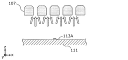
- FIG. 7 is a partial cross-sectional view schematically showing a part of a cross section parallel to the xz plane of the liquid crystal module 100 as viewed from the bottom surface direction.
- the direction of the arrow in the liquid crystal module 100 indicates the light traveling direction, and the length indicates intensity (luminance). Moreover, the difference in the pattern of the arrows indicates that the LEDs 113 that emit light are different. Note that the light that has exceeded the section before entering the luminance uniform plate 107 is not shown for the sake of easy viewing.
- the light transmittance varies depending on the location.
- a description will be given of the difference in transmittance in one compartment that is common to the outer compartment and the inner compartment. Please refer to the solid arrows only.
- the light emitted from the LED 113 is the strongest directly above, and attenuates and weakens as the distance from the LED 113 increases.
- the transmittance of the uniform luminance plate 107 is the lowest in the vicinity of the LED 113 so that the difference in the intensity of light depending on the location becomes smaller after the uniform luminance plate 107 is transmitted, and the length of the arrow indicating the intensity of the light is low. Are greatly different across the brightness uniform plate 107.
- the transmittance is higher in the distance from the LED 113, and the difference in the length of the arrows sandwiching the luminance uniform plate 107 is smaller than the vicinity immediately above the LED 113.
- the transmittance is adjusted so that the difference in the intensity of light after transmission depending on the location is minimized, considering the intensity of light entering from adjacent sections.
- the transmittance is adjusted so that the difference in the intensity of light after transmission depending on the location is minimized, considering the intensity of light entering from adjacent sections.
- the transmittance distribution is compared between the outer section and the inner section to which the second pattern is applied.
- the transmittance changes symmetrically around the vicinity of the LED 113.
- the transmittance changes in the same manner as the inner section in the portion sandwiched between the area immediately above the LED 113 and the adjacent section.
- the change in transmittance across the vicinity of the LED 113 is asymmetric.
- a broken outline arrow indicates light transmitted through the uniform luminance plate 107 in the vicinity of the outer periphery of the array in the second pattern, that is, in the outer section to which the pattern common to the inner section is applied.
- the difference between the dashed outline arrow and the solid outline arrow length is the difference in brightness at this location.
- the incident light is incident.
- the transmittance changes so as to have a negative correlation with the light intensity.
- This change in transmittance is realized by changing the aperture ratio of the through hole provided to transmit light.
- the through holes are arranged in a pattern of partition units facing each light source.
- the production efficiency of the uniform luminance plate may be further taken into consideration.
- the manufacture of the uniform brightness plate 107 can be handled only by changing the mold in the conventional brightness uniform plate manufacturing process.
- the liquid crystal module 100 including the uniform luminance plate 107 In the image display device 10 in which the liquid crystal module 100 including the uniform luminance plate 107 is used, display with higher uniformity of luminance is possible in a continuous region extending from the center to the periphery of the screen.
- the liquid crystal module 100 absorbs the difference in intensity of the light from the direct type backlight depending on the position in the screen, for example, even if the overall thickness is approximately equal, and thereby causes uneven brightness on the entire screen. Can be suppressed.
- Conventionally, such a difference in light intensity has been suppressed by light shielding by ink applied to the diffusion plate in a predetermined pattern by printing, but the uniform luminance plate 107 that can be manufactured with the same efficiency as the conventional one is used.
- the printing process from application of ink to drying can be eliminated from the manufacturing process of the liquid crystal module 100, and the manufacturing cost can be reduced.
- the luminance of the light incident on the luminance uniform plate 107 is more likely to be uneven between the center and the periphery of the screen due to the shape of the lower frame. Also in this case, the brightness uniform plate 107 can suppress uneven brightness on the entire screen by individually adjusting and optimizing the arrangement pattern of the through holes applied to each section.
- the luminance unevenness of the entire screen is suppressed by a device relating to the arrangement pattern of the through holes.
- the luminance unevenness suppressing effect may not be obtained to the same extent by the liquid crystal module. This is due to the fact that the light distribution characteristics of the LED, which is the light source, are different due to differences in the internal structure and the like among the LED models.
- the inventor of the present application absorbs the difference in the light distribution characteristics between the light sources to some extent by taking advantage of the characteristics of the shape of the through-holes opened in the luminance uniform plate 107 using the mold as described above, and is higher.
- the present inventors have found a configuration that obtains an effect of suppressing luminance unevenness. This configuration will be described below with reference to FIGS. 8A and 8B.
- 8A and 8B are schematic partial cross-sectional views of a liquid crystal module for explaining the configuration of the uniform luminance plate 107 in this modification.
- the LED 113A and the LED 113B are arranged on the lower frame 111, respectively.
- the LED 113A and the LED 113B have different light distribution characteristics. More specifically, in the LED 113A, the light traveling in the straight direction (the direction along the z-axis) is strong among the emitted light, and the difference from the light traveling diagonally or laterally is large. In the LED 113B, the light traveling in the straight direction is the strongest, but the difference from the light traveling diagonally or sideways is small.
- the directions of arrows in FIGS. 8A and 8B indicate the traveling direction of typical emitted light, and the length indicates the strength thereof.
- the uniformity of luminance is enhanced by absorbing the difference in the light distribution characteristics by utilizing the sagging generated in the luminance uniform plate 107 by opening a through hole using a mold.
- the sagging surface is directed to the opposite side of the light source. Since the amount of light emitted from the LED 113A is almost straight, there is relatively little light that is blocked by the uniform luminance plate 107 and cannot pass through the through hole in such a configuration. Further, since the light traveling toward the diffusion plate 106 is emitted so as to spread from the sagging surface, it is easy to make the luminance uniform.
- a sagging surface is directed to the light source. That is, relatively strong light emitted from the light source can enter the luminance uniform plate 107 from the wider opening due to the sagging, and is not easily blocked by the luminance uniform plate 107. In other words, more light can be incident and more light can be transmitted as a result than when the uniform luminance plate 107 is used in the configuration shown in FIG. 8A.
- the luminance uniform plate 107 in the above embodiment can be used so as to obtain a higher luminance unevenness suppression effect according to the light distribution characteristics of the light source.
- one type of uniform brightness plate 107 can cope with light sources having different light distribution characteristics, options for light source procurement are expanded.
- the plurality of LEDs 113 are used as light sources, but the above-described embodiment and modification examples can also be applied to a direct backlight type image display apparatus in which a light source other than LEDs is used.
- Examples of the light source other than the LED of the image display device to which each embodiment or modification is applied include a cold cathode tube and a fluorescent tube.
- image display device 10 has been described as a liquid crystal television, for example, other examples include a monitor display for a personal computer and a display for digital signage.
- the present disclosure can be applied to an image display device having an appearance that looks thinner, for example, by suppressing the thickness of the peripheral portion from other portions. More specifically, the present disclosure is applicable to a television receiver, a monitor display, a digital signage display, or the like.
- Image display apparatus 100 Liquid crystal module 101 Bezel 102 Display panel 103 Back cover 104 Mold frame 105 Optical sheet unit 106 Diffuser plate 107 Brightness uniform plate 107A, 107B Partition 107h, 107i, 107j, 107k Opening part 108 Reflective sheet 109 LED sheet 110 Relay Seat 111 Lower frame 111A Flat part 111B Side wall part 112 Support pin 112A Tip part 112B Flange part 113, 113A, 113B LED (light source) 200 stands
Abstract
Provided is an image display device (10) comprising: a display panel (102); a lower frame (111) which includes a flat part (111A) having an approximately flat face; light sources (113) disposed at approximately equal intervals on the flat part (111A); and a luminance equalizing plate (107) separated from the light sources (113) and supported by a plurality of support pins (112). The luminance equalizing plate (107) has a plurality of through-holes which allow emission light of the light sources (113) to pass through to the display panel (102) side. The plurality of through-holes are disposed in a prescribed pattern which is applied to each of sections arranged so as to form arrays on the luminance equalizing plate (107), each section facing one of the light sources (113). The prescribed pattern includes a first pattern which is applied to at least some of the sections in contact with the outer periphery of the array, and a second pattern which is applied to at least some of the sections to which the first pattern is not applied.
Description
本開示は、液晶セル等の表示パネルを備える画像表示装置に関する。
The present disclosure relates to an image display device including a display panel such as a liquid crystal cell.
特許文献1は、輝度ムラが少ない均一な面照明光を得るための光透過反射板を含む面光源ユニットを直下型のバックライトとして用いる表示装置を開示する。
Patent Document 1 discloses a display device that uses a surface light source unit including a light-transmitting / reflecting plate for obtaining uniform surface illumination light with less luminance unevenness as a direct backlight.
本開示は、画面全体で輝度の均一性のより高い表示が可能な画像表示装置を提供する。
The present disclosure provides an image display device capable of displaying with higher uniformity of luminance over the entire screen.
本開示における画像表示装置は、表示パネルと、表示パネルの有効領域と対向する略平坦な面を有する平坦部を含む下フレームと、平坦部に略等間隔で配置される複数の光源と、平坦部に略等間隔で配置される柱状の複数のサポートピンに、複数の光源から離間して支持されるシート状の輝度均一板とを備え、輝度均一板は、複数の光源の出射光を表示パネル側に透過させる複数の貫通孔を有し、複数の貫通孔は、輝度均一板において配列をなす、それぞれが複数の光源のいずれかに対向する複数の区画の各々に適用される所定のパターンで配置され、当該所定のパターンは、複数の区画のうち少なくとも、上記の配列の外周に接する外区画の一部に適用される第一パターンと、複数の区画のうち第一パターンが適用されない区画の少なくとも一部に適用される、第一パターンとは異なる第二パターンとを含む。
An image display device according to the present disclosure includes a display panel, a lower frame including a flat portion having a substantially flat surface facing an effective area of the display panel, a plurality of light sources arranged at substantially equal intervals on the flat portion, A plurality of pillar-shaped support pins arranged at substantially equal intervals in the section are provided with a sheet-like luminance uniform plate supported away from the plurality of light sources, and the luminance uniform plate displays the emitted light of the plurality of light sources. A predetermined pattern applied to each of a plurality of partitions each having a plurality of through-holes to be transmitted to the panel side, each of the plurality of through-holes being arranged in a uniform luminance plate, each facing one of the plurality of light sources. The predetermined pattern includes a first pattern that is applied to at least a part of the outer partition that touches the outer periphery of the array, and a partition in which the first pattern is not applied among the plurality of partitions. Less It is also applied to a part, and a different second pattern from the first pattern.
本開示における画像表示装置によれば、画面全体で輝度の均一性のより高い表示が可能である。
According to the image display device of the present disclosure, it is possible to display with higher luminance uniformity over the entire screen.
本願発明者は、従来の画像表示装置に関し、以下の問題が生じることを見出した。
The inventor of the present application has found that the following problems occur with respect to a conventional image display device.
従来の液晶テレビ等の画像表示装置では、表示パネルを取り囲むように含む表示モジュールは、大まかには前後に薄い直方体であるが、より厳密には、その背面側の四辺が比較的大きく面取りされたような形状を有する。このような端面での厚さの小さい形状とすることで、表示モジュールそのものを薄く見せるという外観上の効果を得ている。
In a conventional image display device such as a liquid crystal television, a display module including a display panel is roughly a thin rectangular parallelepiped on the front and back, but more strictly, the four sides on the back side are relatively large and chamfered. It has such a shape. By adopting such a shape with a small thickness at the end face, an appearance effect is obtained that makes the display module itself appear thin.
このような形状の表示モジュールの内部では、周辺部分における厚さがその他の部分での厚さに比べて小さい。
In the display module having such a shape, the thickness in the peripheral portion is smaller than the thickness in other portions.
ところがこのような画像表示装置では、表示パネルの周辺部分においては内部空間の厚さ方向の制約上、その他の部分と共通の表示機構が採用できない。そのため、画面全体で均一な画質を得るのが困難であるという問題がある。具体例を挙げると、直下型バックライト方式を用いる画像表示装置では、複数の光源のうち表示パネルの最も外側にある光源におもに照らされる区画には、その他の区画とは異なり、入射する光には、入射面に対して斜めの面からの反射光が含まれるため光量が少ない。また、光源に照らされる隣接の区画が表示パネルの端部方向に存在しない。したがってそのような区画では、表示パネルのより内側にあって、全方向にある隣接の区画からも光が入る区画と異なり、表示パネルの端部付近の部分でも他の部分と同程度に高い輝度を得るのが困難である。つまり画面の端部付近で、端部に向かってより暗くなる輝度ムラが生じる。
However, in such an image display device, a display mechanism common to other parts cannot be adopted in the peripheral part of the display panel due to the limitation of the thickness direction of the internal space. Therefore, there is a problem that it is difficult to obtain uniform image quality over the entire screen. To give a specific example, in an image display device using a direct type backlight system, a section illuminated mainly by a light source on the outermost side of a display panel among a plurality of light sources differs from the other sections in incident light. Has a small amount of light because it includes reflected light from a surface oblique to the incident surface. Further, there is no adjacent section illuminated by the light source in the direction of the edge of the display panel. Therefore, in such a section, unlike the section where light enters from the adjacent section in all directions inside the display panel, the brightness near the edge of the display panel is as high as other parts. Is difficult to get. That is, luminance unevenness that becomes darker toward the end portion occurs near the end portion of the screen.
なお、上記のような薄く見せる効果を奏する形状ではなく、薄い直方体に近い形状の表示モジュールでも同様の輝度ムラは生じ得る。このような画像表示装置では、下フレームの形状の工夫、又は反射シート若しくは拡散板への印刷である程度抑えられている。しかしながら上述のように、表示モジュールを薄く見せるための形状の制約が下フレームにあるために、隣接する区画から入る光量の表示パネル内の区画間での違いが複雑であり、反射シート等への印刷による輝度ムラの抑制が困難である。
It should be noted that the same luminance unevenness may occur even in a display module having a shape close to a thin rectangular parallelepiped instead of a shape that exhibits the effect of making it look thin as described above. In such an image display device, it is suppressed to some extent by devising the shape of the lower frame or printing on a reflection sheet or a diffusion plate. However, as described above, since the lower frame has a shape restriction to make the display module appear thin, the difference in the amount of light entering from the adjacent sections between the sections in the display panel is complicated, and the reflection sheet or the like It is difficult to suppress luminance unevenness due to printing.
本開示はこのような知見に基づいてなされたものであり、本願発明者は、画面全体で輝度の均一性のより高い表示が可能な画像表示装置の構造の着想を得た。
The present disclosure has been made on the basis of such knowledge, and the inventor of the present application has obtained an idea of the structure of an image display device capable of displaying with higher luminance uniformity over the entire screen.
以下、適宜図面を参照しながら実施の形態を説明する。ただし、必要以上に詳細な説明は省略する場合がある。例えば、既によく知られた事項の詳細説明や実質的に同一の構成に対する重複説明を省略する場合がある。これは、以下の説明が不必要に冗長になるのを避け、当業者の理解を容易にするためである。
Hereinafter, embodiments will be described with reference to the drawings as appropriate. However, more detailed explanation than necessary may be omitted. For example, detailed descriptions of already well-known matters and repeated descriptions for substantially the same configuration may be omitted. This is to avoid the following description from becoming unnecessarily redundant and to facilitate understanding by those skilled in the art.
なお、本願発明者は、当業者が本開示を十分に理解するために添付図面および以下の説明を提供するのであって、これらによって請求の範囲に記載の主題を限定することを意図するものではない。
In addition, the inventor of the present application provides the accompanying drawings and the following description in order for those skilled in the art to fully understand the present disclosure, and is not intended to limit the subject matter described in the claims. Absent.
以下、液晶テレビを構成する画像表示装置を例に用いて、図を参照して複数の実施の形態について説明するが、それに先立って、実施の形態及びその変形例に共通して関連する画像表示装置の構造の概要について説明する。実施の形態間での差異は後述する。
Hereinafter, a plurality of embodiments will be described with reference to the drawings by using an image display device constituting a liquid crystal television as an example, but prior to that, image display commonly related to the embodiments and modifications thereof will be described. An outline of the structure of the apparatus will be described. Differences between the embodiments will be described later.
また、以下の実施の形態において、説明の便宜上、画像表示装置の上下方向をy軸の方向と一致させ、前後方向をz軸の方向と一致させ、左右方向をx軸の方向と一致させている。ただし、これらの方向の対応付けは、本開示に係る画像表示装置の製造時又は使用時における姿勢を限定するものではない。
In the following embodiments, for convenience of explanation, the vertical direction of the image display device is matched with the y-axis direction, the front-rear direction is matched with the z-axis direction, and the horizontal direction is matched with the x-axis direction. Yes. However, the association of these directions does not limit the posture at the time of manufacturing or using the image display apparatus according to the present disclosure.
(画像表示装置の構成概要)
図1は、各実施の形態に係る画像表示装置10の外観斜視図である。図2及び図3はそれぞれ、各実施の形態に係る液晶モジュール100の分解斜視図である。 (Outline of image display device configuration)
FIG. 1 is an external perspective view of animage display apparatus 10 according to each embodiment. 2 and 3 are exploded perspective views of the liquid crystal module 100 according to each embodiment.
図1は、各実施の形態に係る画像表示装置10の外観斜視図である。図2及び図3はそれぞれ、各実施の形態に係る液晶モジュール100の分解斜視図である。 (Outline of image display device configuration)
FIG. 1 is an external perspective view of an
画像表示装置10は例えば液晶テレビであり、図1に示されるように、液晶モジュール100と、ベゼル101と、バックカバー103と、スタンド200とを備える。
The image display device 10 is, for example, a liquid crystal television, and includes a liquid crystal module 100, a bezel 101, a back cover 103, and a stand 200 as shown in FIG.
液晶モジュール100は静止画及び動画を表示可能な映像表示のためのモジュールであり、表示パネル102を備える。
The liquid crystal module 100 is a module for displaying images that can display still images and moving images, and includes a display panel 102.
表示パネル102は、以下に説明する各実施の形態では、いわゆる液晶セルであり、複数のガラス板の間に液晶が封入された素子である。表示パネル102は、画像表示装置10に入力された映像信号に基づいて制御され、映像を表示する。
In each embodiment described below, the display panel 102 is a so-called liquid crystal cell, and is an element in which liquid crystal is sealed between a plurality of glass plates. The display panel 102 is controlled based on the video signal input to the image display device 10 and displays a video.
また、液晶モジュール100は、スタンド200を用いて、床又は台の上に立てることができる。ただし、液晶モジュール100の使用態様はこれに限定されない。例えば液晶モジュール100は、スタンド200を用いずに、他の取付具を用いて壁に掛けられるか又は埋め込まれたり、天井から吊り下げられたりしての画像表示装置10としての使用が可能であってもよい。
In addition, the liquid crystal module 100 can be set on a floor or a stand using the stand 200. However, the usage mode of the liquid crystal module 100 is not limited to this. For example, the liquid crystal module 100 can be used as the image display device 10 by being hung on a wall or embedded using another fixture, or suspended from the ceiling without using the stand 200. May be.
樹脂で形成されるベゼル101は、画像表示装置10の四辺それぞれに対応するよう分割して形成され、例えばネジを用いて相互に結合される。ベゼル101は、後述の表示パネル102から下フレーム111までの複数の部品を、バックカバー103と共に挟持する。
The bezel 101 made of resin is divided and formed so as to correspond to each of the four sides of the image display device 10, and is coupled to each other using, for example, screws. The bezel 101 sandwiches a plurality of components from a display panel 102 (described later) to a lower frame 111 together with the back cover 103.
上記構成を有する液晶モジュール100はさらに、図2又は図3に示されるように、モールドフレーム104と、光学シートユニット105と、拡散板106と、輝度均一板107と、反射シート108と、LEDシート109と、中継シート110と、下フレーム111と、サポートピン112とを備える。
As shown in FIG. 2 or FIG. 3, the liquid crystal module 100 having the above configuration further includes a mold frame 104, an optical sheet unit 105, a diffusion plate 106, a luminance uniform plate 107, a reflection sheet 108, and an LED sheet. 109, a relay sheet 110, a lower frame 111, and support pins 112.
モールドフレーム104は、光学シートユニット105からLEDシート109及び中継シート110までの複数の部品(いわゆるバックライトユニット)を、下フレーム111と挟んで支持する。なお、図3ではモールドフレーム104の図示を省略している。
The mold frame 104 supports a plurality of components (so-called backlight units) from the optical sheet unit 105 to the LED sheet 109 and the relay sheet 110 with the lower frame 111 interposed therebetween. In FIG. 3, the mold frame 104 is not shown.
光学シートユニット105は、光学特性の異なる2、3種類のシートを複数枚重ねて構成される。例えば、光学シートユニット105には、縦方向のプリズムシート、横方向のプリズムシート及び拡散シートが含まれる。
The optical sheet unit 105 is configured by stacking a plurality of two or three types of sheets having different optical characteristics. For example, the optical sheet unit 105 includes a vertical prism sheet, a horizontal prism sheet, and a diffusion sheet.
拡散板106は、LEDシート109上に配置された、画像表示装置10の光源である複数のLED(Light-Emitting Diode)113から入射する光を拡散して、表示パネル102に向けて出射する。
The diffusion plate 106 diffuses light incident from a plurality of LEDs (Light-Emitting Diodes) 113 disposed on the LED sheet 109 and serving as a light source of the image display device 10, and emits the light toward the display panel 102.
輝度均一板107は、LEDシート109上に配置された複数のLED113からの光(以下、出射光ともいう)を、場所によって異なる輝度の均一度を高めて拡散板106及び表示パネル102がある側に透過させる。輝度均一板107は、例えば微細な気泡を密に含むPET(polyethylene terephthalate)等の樹脂製で、良好な光反射性を有するシート状の部材である。
The luminance uniform plate 107 is a side on which the diffuser 106 and the display panel 102 are provided by increasing the uniformity of the luminance of the light from the plurality of LEDs 113 arranged on the LED sheet 109 (hereinafter also referred to as outgoing light), which varies depending on the location. Make it transparent. The uniform brightness plate 107 is a sheet-like member made of a resin such as PET (polyethylene terephthalate) that contains fine bubbles densely and has good light reflectivity.
輝度均一板107には、略全体にわたって貫通孔が多数形成されている。LED113の出射光は、その一部がこれらの貫通孔を通って反対側、つまり表示パネル102及び拡散板106のある側に抜ける(本開示では「光が輝度均一板107を透過する」とも表現している)。輝度均一板107は、離間した所定の位置にある光源からの光の単位面積当たりの透過量を均一に近づけるようにこれらの貫通孔の個数、大きさ、又は分布が調整されている。つまり、輝度均一板107に設けられる貫通孔のすべてが均一な大きさであったり、又は均等に分布したりするわけではない。このような貫通孔は、輝度均一板107において配列をなしている、それぞれがLED113のいずれかに対向する複数の区画の各々に適用される所定のパターンで配置される。輝度均一板107は、例えば所定の大きさの上記の樹脂製のシートに、金型を用いてこのようなパターンに配置された貫通孔を開けることで製造される。
The luminance uniform plate 107 has a large number of through-holes formed over substantially the whole. A part of the light emitted from the LED 113 passes through these through holes to the opposite side, that is, the side where the display panel 102 and the diffusion plate 106 are present (in the present disclosure, it is also expressed as “light passes through the luminance uniform plate 107”). is doing). In the uniform brightness plate 107, the number, size, or distribution of these through holes are adjusted so that the transmission amount per unit area of light from a light source located at a predetermined position apart from each other can be made uniform. That is, all the through holes provided in the luminance uniform plate 107 are not uniformly sized or evenly distributed. Such through-holes are arranged in a predetermined pattern applied to each of a plurality of sections that are arranged on the luminance uniform plate 107 and that face each of the LEDs 113. The uniform luminance plate 107 is manufactured by, for example, opening through holes arranged in such a pattern using a mold in the resin sheet having a predetermined size.
なお、図2及び図3における輝度均一板107上の桝目は、このような複数の区画があることを示す。ただし、輝度均一板107をこれらの桝目に区切る線は仮想線であり、実際にこのような線が引かれているわけではない。以下の図面においても同様である。所定のパターンについては、実施の形態で後述する。
Note that the grids on the uniform luminance plate 107 in FIGS. 2 and 3 indicate that there are a plurality of such sections. However, the line dividing the uniform brightness plate 107 into these cells is a virtual line, and such a line is not actually drawn. The same applies to the following drawings. The predetermined pattern will be described later in the embodiment.
この構成によって、LED113が出射した光の配向特性(以下、配光特性ともいう)がなだらかにされる。輝度均一板107によって配光特性がなだらかにされたLED113からの光は、拡散板106によって輝度ムラがさらに抑えられるよう拡散されてから表示パネル102に向けて出射される。
With this configuration, the alignment characteristic (hereinafter also referred to as light distribution characteristic) of the light emitted from the LED 113 is smoothed. The light from the LED 113 whose light distribution characteristics have been smoothed by the uniform luminance plate 107 is diffused by the diffusion plate 106 so that the luminance unevenness is further suppressed and then emitted toward the display panel 102.
反射シート108は、LEDシート109上に配置された複数のLED113のそれぞれに対応する位置及び大きさの孔が設けられたシートであり、画像表示装置10の正面側の面全体で光を反射する。反射シート108は、表示パネル102の有効領域と対向し、この有効領域より小さい略平坦な面を有する平坦部と、平坦部の四辺の端部から立ちあがり、画像表示装置10の正面側から見て表示パネル102の有効領域の外縁に達する側壁部とを含み、全体として後述の下フレーム111に概ね沿う形状を有する。
The reflection sheet 108 is a sheet in which holes having positions and sizes corresponding to the plurality of LEDs 113 arranged on the LED sheet 109 are provided, and reflects light on the entire front surface of the image display device 10. . The reflection sheet 108 faces the effective area of the display panel 102, rises from a flat portion having a substantially flat surface smaller than the effective area, and ends of the four sides of the flat portion, and is viewed from the front side of the image display device 10. And a side wall portion that reaches the outer edge of the effective area of the display panel 102, and has a shape that generally follows the lower frame 111 described later.
LEDシート109は、複数のLED113が配置されたフレキシブルプリント基板(以下、FPC(Flexible Printed Circuitsの頭字語)という)である。LED113はシート状のFPCの2つの主面の一方に配置され、FPCのLEDが配置されている主面、つまりは画像表示装置10の正面側の主面には、光を反射する反射層が形成される。また、LEDシート109の主面にある複数のLED113は、表示パネル102の背面の極力広い範囲を、場所によるムラを極力抑えて照射できるよう、略等間隔で、例えば行列状に配置される。
The LED sheet 109 is a flexible printed circuit board (hereinafter referred to as FPC (Flexible Printed Circuits)) on which a plurality of LEDs 113 are arranged. The LED 113 is disposed on one of the two main surfaces of the sheet-like FPC, and a reflective layer that reflects light is disposed on the main surface on which the FPC LED is disposed, that is, the main surface on the front side of the image display device 10. It is formed. In addition, the plurality of LEDs 113 on the main surface of the LED sheet 109 are arranged at substantially equal intervals, for example, in a matrix form so that a wide range on the back surface of the display panel 102 can be irradiated with as little unevenness as possible.
中継シート110は、LEDシート109に配置されている各LED113へ電力及び制御信号などを送るための電気経路が形成されたFPCである。また、中継シート110では、LEDシート109と同様に、画像表示装置10の正面側の主面に反射層が形成される。
The relay sheet 110 is an FPC in which an electrical path for sending electric power, a control signal, and the like to each LED 113 arranged on the LED sheet 109 is formed. Further, in the relay sheet 110, similarly to the LED sheet 109, a reflective layer is formed on the main surface on the front side of the image display device 10.
下フレーム111は薄い板金で形成される板状の部材であってベースプレートとも称され、LEDシート109及び中継シート110を支持する。下フレーム111は、表示パネル102の有効領域と対向し、この有効領域より小さい略平坦な面を有する平坦部111Aと、平坦部111Aの外縁、つまり四辺の端部から立ちあがり、画像表示装置10の正面側(表示パネル102のある側)から見て表示パネル102の有効領域の外縁に達する側壁部111Bとを含む。バックカバー103を下フレーム111の外形に沿った形状にすることで、液晶モジュール100は上述の、前後(z軸に沿う方向)に薄い直方体から背面側の四辺が大きく面取りされたような形状による、より薄く見えるという外観上の効果を奏している。
The lower frame 111 is a plate-like member formed of a thin sheet metal and is also referred to as a base plate, and supports the LED sheet 109 and the relay sheet 110. The lower frame 111 opposes the effective area of the display panel 102 and rises from a flat portion 111A having a substantially flat surface smaller than the effective area, and from the outer edge of the flat portion 111A, that is, from the ends of the four sides. And a side wall portion 111 </ b> B reaching the outer edge of the effective area of the display panel 102 when viewed from the front side (side with the display panel 102). By forming the back cover 103 along the outer shape of the lower frame 111, the liquid crystal module 100 has a shape in which the four sides on the back side are greatly chamfered from the thin rectangular parallelepiped in the front-rear direction (the direction along the z axis). It has the effect of appearance that looks thinner.
なお、以下の各実施の形態で説明される構成は、上記のような効果を奏さない構成の下フレーム及び反射シートを備える液晶モジュールにも、表示パネル102の有効領域全体にわたる輝度の均一性を高めるために適用可能である点に留意されたい。
Note that the configurations described in the following embodiments also provide luminance uniformity over the entire effective area of the display panel 102 in a liquid crystal module including a lower frame and a reflective sheet that do not exhibit the above effects. Note that it can be applied to enhance.
また、下フレーム111の平坦部111Aには、光源である複数のLED113が配置される。より具体的には、複数のLED113が略等間隔で配置されたLEDシート109及び中継シート110が平坦部111Aに取り付けられる。その後、さらに反射シート108が、反射シート108の複数の孔から各LED113が露出するように貼り付けられる。各LED113の出射光は、直接、又はFPCに形成された反射層及び反射シート108によって反射されて、各LED113に対して画像表示装置10の正面側にある輝度均一板107に入射する。下フレーム111はさらに、光学シートユニット105からLEDシート109及び中継シート110までのバックライトユニットを、モールドフレーム104と挟んで支持する。
Further, a plurality of LEDs 113 as light sources are arranged on the flat portion 111A of the lower frame 111. More specifically, the LED sheet 109 and the relay sheet 110 in which the plurality of LEDs 113 are arranged at substantially equal intervals are attached to the flat portion 111A. Thereafter, the reflection sheet 108 is further attached so that each LED 113 is exposed from the plurality of holes of the reflection sheet 108. The light emitted from each LED 113 is reflected directly or by the reflection layer and the reflection sheet 108 formed on the FPC, and is incident on the luminance uniform plate 107 on the front side of the image display device 10 with respect to each LED 113. The lower frame 111 further supports the backlight unit from the optical sheet unit 105 to the LED sheet 109 and the relay sheet 110 with the mold frame 104 interposed therebetween.
下フレーム111はバックライトユニット各構成を支持するための構成をさらに有してもよい。例えば、下フレーム111には、画像表示装置10を使用状態に置いたときに上側となる一辺の近辺に、光学シートユニット105を吊り下げる切り起こしが形成されていてもよい。この場合、光学シートユニット105には、例えばこの切り起こしに引っ掛けるための孔を有するタブが設けられる。
The lower frame 111 may further have a structure for supporting each structure of the backlight unit. For example, the lower frame 111 may have a cut-and-raised part that hangs the optical sheet unit 105 in the vicinity of the upper side when the image display device 10 is put into use. In this case, the optical sheet unit 105 is provided with, for example, a tab having a hole for hooking it.
図3に示される複数のサポートピン112は、柱状の部材である。各サポートピン112は、下フレーム111に取り付けられる端部と反対側の端部である先端部112Aと、柱状の形状の長手方向の途中にある鍔状のフランジ部112Bを有する。
The plurality of support pins 112 shown in FIG. 3 are columnar members. Each support pin 112 has a tip end portion 112A which is an end portion on the opposite side to the end portion attached to the lower frame 111, and a flange-like flange portion 112B in the middle of the columnar shape in the longitudinal direction.
複数のサポートピン112は、反射シート108越しに下フレーム111の平坦部111Aに取り付けられ、反射シート108を下フレーム111と挟んで支持する。
The plurality of support pins 112 are attached to the flat portion 111A of the lower frame 111 through the reflection sheet 108, and support the reflection sheet 108 with the lower frame 111 interposed therebetween.
また、複数のサポートピン112は、拡散板106及び輝度均一板107を支持する。図4は、液晶モジュール100の内部で下フレーム111に取り付けられたサポートピン112が拡散板106及び輝度均一板107を支持する様子を説明するための模式図である。ただし、図4では、液晶モジュール100の構成のうち、この説明に必要ないものは図示を省略している。
Also, the plurality of support pins 112 support the diffusion plate 106 and the luminance uniform plate 107. FIG. 4 is a schematic diagram for explaining how the support pins 112 attached to the lower frame 111 support the diffusion plate 106 and the luminance uniform plate 107 inside the liquid crystal module 100. However, in FIG. 4, the configuration of the liquid crystal module 100 that is not necessary for this description is omitted.
輝度均一板107には、下フレーム111に取り付けられた複数のサポートピン112のそれぞれに対応する位置に、サポートピン112を挿入するための孔が設けられている。輝度均一板107は、この孔にサポートピン112が先端部112Aから挿入されて、図4に示されるように、サポートピン112のフランジ部112Bで支持されるように取り付けられる。
The brightness uniform plate 107 is provided with holes for inserting the support pins 112 at positions corresponding to the plurality of support pins 112 attached to the lower frame 111. The brightness uniform plate 107 is attached so that the support pin 112 is inserted into the hole from the tip end portion 112A and supported by the flange portion 112B of the support pin 112 as shown in FIG.
なお、サポートピン112は、設計上決定される、下フレーム111上のLED113から離間した位置に輝度均一板107を支持すればよく、この支持のための構成は、鍔状のフランジ部112Bに限定されない。例えばサポートピン112は、フランジ部112Bに代えて頂面のある台座のような部分を有し、この部分の頂面で輝度均一板107を支持してもよい。または、サポートピン112は、取付時に液晶モジュール100の正面から背面に向かって太くなる部分を有し、この部分と輝度均一板107の孔の径が一致する場所で輝度均一板107を支持してもよい。
The support pin 112 may support the luminance uniform plate 107 at a position determined from the design and spaced from the LED 113 on the lower frame 111, and the configuration for this support is limited to the flange-shaped flange portion 112B. Not. For example, the support pin 112 may have a base-like portion with a top surface instead of the flange portion 112B, and the luminance uniform plate 107 may be supported by the top surface of this portion. Alternatively, the support pin 112 has a portion that becomes thicker from the front to the back of the liquid crystal module 100 when attached, and supports the luminance uniform plate 107 at a place where the diameter of the hole of the luminance uniform plate 107 coincides with this portion. Also good.
また、拡散板106は、周辺において下フレーム111の側壁部111Bの端部で支持されるとともに、周辺以外の部分では、図4に示されるように、下フレーム111の平坦部111Aに立設するサポートピン112の先端部112Aで支持される。
In addition, the diffusion plate 106 is supported by the end of the side wall 111B of the lower frame 111 in the periphery, and is erected on the flat portion 111A of the lower frame 111 as shown in FIG. It is supported by the tip 112A of the support pin 112.
このようなサポートピン112は、平坦部111Aにおいて、拡散板106及び輝度均一板107の全体を支えられるよう、略等間隔で、例えば行列状に配置される。また、輝度均一板107に向かう光を極力遮らないよう、サポートピン112は、各LED113から離れた位置、例えば、行列方向に隣接する2個のLED113から等距離の点を結ぶ直線上に配置される。
Such support pins 112 are arranged at substantially equal intervals, for example, in a matrix form so as to support the entire diffuser plate 106 and luminance uniform plate 107 in the flat portion 111A. Further, the support pin 112 is arranged at a position away from each LED 113, for example, on a straight line connecting two equidistant points from the two LEDs 113 adjacent in the matrix direction so as not to block the light toward the luminance uniform plate 107 as much as possible. The
このような本開示に係る画像表示装置10において、画面全体で輝度の均一性をより高めるための液晶モジュール100の構成を以下に説明する。
In the image display apparatus 10 according to the present disclosure as described above, the configuration of the liquid crystal module 100 for further improving the uniformity of luminance over the entire screen will be described below.
(実施の形態)
図5は、実施の形態に係る液晶モジュール100の構成を、例を用いて説明するための模式図である。 (Embodiment)
FIG. 5 is a schematic diagram for explaining the configuration of theliquid crystal module 100 according to the embodiment using an example.
図5は、実施の形態に係る液晶モジュール100の構成を、例を用いて説明するための模式図である。 (Embodiment)
FIG. 5 is a schematic diagram for explaining the configuration of the
より具体的には、(a)は、輝度均一板107の複数の区画のうち、3つの区画の拡大正面図である。
More specifically, (a) is an enlarged front view of three sections among a plurality of sections of the uniform brightness plate 107.
(b)は、輝度均一板107全体の模式的な正面図である。上述のとおり、輝度均一板107において配列をなす桝目状の区画の境界が仮想線で示される。(b)から(a)に伸びる矢印は、(b)に示す全体図における位置と(a)に示す拡大図の位置との対応を示す。
(B) is a schematic front view of the entire luminance uniform plate 107. As described above, the boundaries of the grid-like sections that are arranged on the luminance uniform plate 107 are indicated by virtual lines. The arrow extending from (b) to (a) indicates the correspondence between the position in the overall view shown in (b) and the position in the enlarged view shown in (a).
(a)及び(b)に複数ある破線の矩形は、平坦部111Aに配置されているLED113の正面視における位置を示す。各区画は、下フレーム111の平坦部111Aに配置されているLED113のいずれかに対向する。
(A) and a plurality of broken rectangles in (b) indicate the positions of the LEDs 113 arranged on the flat portion 111A in a front view. Each section faces one of the LEDs 113 arranged on the flat portion 111A of the lower frame 111.
(c)は、液晶モジュール100のxz平面に平行な断面を底面方向から見た図である。
(C) is the figure which looked at the cross section parallel to xz plane of the liquid crystal module 100 from the bottom face direction.
(b)及び(c)に跨る2本の点線は、下フレーム111の平坦部111Aと側壁部111Bとの境界に対応する位置を示す。この位置は、(a)の拡大図においても同じ外観の点線で示されている。
The two dotted lines extending over (b) and (c) indicate positions corresponding to the boundary between the flat portion 111A and the side wall portion 111B of the lower frame 111. This position is indicated by a dotted line having the same appearance in the enlarged view of (a).
以下、図5を参照して、輝度均一板107を中心に本実施の形態に係る液晶モジュール100の構成を説明する。
Hereinafter, the configuration of the liquid crystal module 100 according to the present embodiment will be described with reference to FIG.
図5の(a)の複数の円は、輝度均一板107に開けられている貫通孔の開口部をそれぞれ示す。開口部107h、107i、107j、及び107kは、以下の説明で例に用いる貫通孔の開口部である。同じ大きさの開口部には共通の参照符号が付されている。なお、(b)では、これらの貫通孔の開口部は図示が省略されている。
5A. Each of the plurality of circles in FIG. 5A indicates an opening of a through hole formed in the luminance uniform plate 107. The openings 107h, 107i, 107j, and 107k are through-hole openings used for examples in the following description. Common reference numerals are assigned to openings of the same size. In addition, in (b), illustration of the opening part of these through-holes is abbreviate | omitted.
貫通孔は、各区画に適用される所定のパターンで配置される。本実施の形態において、ひとつの輝度均一板107で用いられる所定のパターンには複数のパターンが含まれる。そして各区画に適用されるパターンは、複数の区画がなす配列における当該区画の位置によって異なる。より具体的には、図5に示される例では、区画の配列の左右両端に位置する列に含まれる区画と、その間にある列に含まれる区画とで適用されるパターンが異なる。ここでは、左右両端の列に含まれる各区画を区画107B、その間にある列に含まれる各区画を区画107Aと呼ぶ。つまり、(a)に示す3つの区画は、左から右に向かって区画107B、区画107A、区画107Bの順に並んでいる。区画107Bは、本実施の形態において後述する外区画の例である。
The through holes are arranged in a predetermined pattern applied to each section. In the present embodiment, the predetermined pattern used in one luminance uniform plate 107 includes a plurality of patterns. And the pattern applied to each division changes with the position of the said division in the arrangement | sequence which a some division makes. More specifically, in the example shown in FIG. 5, the pattern applied differs between the sections included in the columns located at the left and right ends of the array of sections and the sections included in the columns in between. Here, each section included in the left and right columns is referred to as a section 107B, and each section included in a column between them is referred to as a section 107A. That is, the three sections shown in (a) are arranged in the order of section 107B, section 107A, and section 107B from left to right. The section 107B is an example of an outer section described later in the present embodiment.
(a)を参照すると、所定のパターンのひとつが適用されている区画107Aでは、対向するLED113から遠い貫通孔ほど概して開口面積が大きい。例えば開口部107h及び開口部107iのいずれも、区画107Aの中央と重なる位置にあるLED113からより近い貫通孔の開口部よりも大きい。また、開口部107hと開口部107iとを比較すると、LED113からより遠い貫通孔の開口部107hの方が大きい。
Referring to (a), in the section 107A to which one of the predetermined patterns is applied, the opening area farther from the facing LED 113 generally has a larger opening area. For example, both of the opening 107h and the opening 107i are larger than the opening of the through hole closer to the LED 113 at the position overlapping the center of the section 107A. Further, when comparing the opening 107h and the opening 107i, the opening 107h of the through hole farther from the LED 113 is larger.
輝度均一板107では、光の透過率は、単位面積当たりの開口面積(以下、開口率という)にしたがって変化する。ここでいう単位面積は、ひとつの区画全体の面積よりは小さく、ひとつの貫通孔の開口面積として最大のものよりは大きく定めることができる。上述のように、ひとつの区画内で複数の貫通孔の開口面積に変化を付けることで、その区画内での開口率に、場所による差が付けることができる。これにより、区画107Aの中での出射光の透過率は、LED113からより近い場所ではより低く、より遠い場所ではより高く調整される。その結果、区画107Bで輝度均一板107を表示パネル102側に透過した光の輝度を空間的に均一な状態に近づけることができる。
In the uniform luminance plate 107, the light transmittance changes according to the opening area per unit area (hereinafter referred to as the opening ratio). The unit area here can be determined to be smaller than the entire area of one section and larger than the maximum opening area of one through hole. As described above, by changing the opening area of the plurality of through holes in one section, it is possible to add a difference in location to the opening ratio in the section. Thereby, the transmittance of the emitted light in the section 107A is adjusted to be lower at a location closer to the LED 113 and higher at a location farther away. As a result, the brightness of the light transmitted through the brightness uniform plate 107 to the display panel 102 side in the partition 107B can be made to be close to a spatially uniform state.
これに対し、所定のパターンの他のひとつが適用されている区画107Bでは、対向するLED113から遠い貫通孔ほど概して開口面積が大きいという傾向がある。例えば、開口部107hと開口部107iとを比較すると、LED113からより遠い貫通孔の開口部107hの方が大きい。同様に、開口部107jと開口部107kとを比較すると、LED113からより遠い貫通孔の開口部107jの方が大きい。
On the other hand, in the section 107B to which another one of the predetermined patterns is applied, there is a tendency that the opening area is generally larger as the through hole is farther from the facing LED 113. For example, when comparing the opening 107h and the opening 107i, the opening 107h of the through hole farther from the LED 113 is larger. Similarly, when comparing the opening 107j and the opening 107k, the opening 107j of the through hole farther from the LED 113 is larger.
また、さらに、区画の配列の外周からより近い貫通孔は、LED113からの距離は同程度であっても、この外周からより遠くにある貫通孔よりも開口面積が大きい。例えば、開口部107hと開口部107jとを比較すると、LED113からより遠い貫通孔の開口部107jの方が大きい。同様に、開口部107iと開口部107kとを比較すると、LED113からより遠い貫通孔の開口部107kの方が大きい。
Further, the through hole closer to the outer periphery of the array of sections has a larger opening area than the through hole located farther from the outer periphery even if the distance from the LED 113 is the same. For example, when comparing the opening 107h and the opening 107j, the opening 107j of the through hole farther from the LED 113 is larger. Similarly, when comparing the opening 107i and the opening 107k, the opening 107k of the through hole farther from the LED 113 is larger.
このような貫通孔の開口部の面積の差は、輝度均一板107の左右にある区画107Bに共通して設けられている。なお、この例では、開口部107hと開口部107j、及び開口部107iと開口部107kとでは径に10%程度の差がある。
Such a difference in the area of the opening of the through hole is provided in common to the right and left sections 107B of the luminance uniform plate 107. In this example, there is a difference of about 10% in diameter between the opening 107h and the opening 107j and between the opening 107i and the opening 107k.
これにより、区画107Bの中での出射光の透過率は、LED113からより近い場所ではより低く、より遠い場所ではより高く調整され、表示パネル102側に透過した光の輝度を空間的に均一な状態に近づけることができる。また、あわせて、隣接する区画に対向するLED113からの光が入らない、表示パネル102の端部からより近い場所では、LED113からの距離が同じであっても表示パネル102の端部からより遠い場所よりも高く調整される。その結果、区画107Bで輝度均一板107を表示パネル102側に透過した光の輝度を、空間的に均一な状態に近づけることができる。
Thereby, the transmittance of the emitted light in the section 107B is adjusted to be lower at a location closer to the LED 113 and higher at a location farther away, and the brightness of the light transmitted to the display panel 102 side is spatially uniform. Can be close to the state. In addition, in a place closer to the end of the display panel 102 where light from the LED 113 facing the adjacent section does not enter, even if the distance from the LED 113 is the same, it is farther from the end of the display panel 102. Adjusted higher than the location. As a result, the brightness of the light transmitted through the brightness uniform plate 107 to the display panel 102 side in the section 107B can be brought close to a spatially uniform state.
なお、ひとつの区画に開口面積の異なる複数の貫通孔を配置するのは、その区画内で開口率を変化させるための貫通孔の配置の一例である。開口率を変化させる貫通孔の配置の他の例としては、開口面積の等しい貫通孔の密度(開口の中心間の距離)を区画内で変化させる配置、及び貫通孔の開口面積及び密度の両方を区画内で変化させる配置が挙げられる。また、開口の形状は図5に示されるような円形に限定されず、スリット状であってもよいし、多角形等その他の任意の形状でもよい。
In addition, arranging a plurality of through holes having different opening areas in one section is an example of arranging the through holes for changing the opening ratio in the section. Other examples of the arrangement of the through holes that change the aperture ratio include an arrangement that changes the density of the through holes having the same opening area (distance between the centers of the openings) within the compartment, and both the opening area and the density of the through holes. There is an arrangement in which the value is changed in the compartment. Further, the shape of the opening is not limited to the circular shape as shown in FIG. 5, and may be a slit shape or any other shape such as a polygon.
貫通孔の配置がこれらのいずれであっても、上記のパターンが適用されている区画107Aでは、複数の貫通孔による輝度均一板107の開口率と、当該区画107Aが対向するLED113からの距離とは正の相関を有する。このパターンを、以下では第二パターンともいう。また、上記のパターンが適用されている区画107Bでは、複数の貫通孔による輝度均一板107の開口率と、当該区画107Bが対向するLED113からの距離とは正の相関を有し、かつ開口率と区画の配列の外周からの距離とが負の相関を有する。このパターンを、以下では第一パターンともいう。
Regardless of the arrangement of the through holes, in the section 107A to which the above pattern is applied, the aperture ratio of the luminance uniform plate 107 by the plurality of through holes and the distance from the LED 113 facing the section 107A Has a positive correlation. Hereinafter, this pattern is also referred to as a second pattern. In the section 107B to which the above pattern is applied, the aperture ratio of the luminance uniform plate 107 by a plurality of through holes and the distance from the LED 113 facing the section 107B have a positive correlation, and the aperture ratio. And the distance from the outer circumference of the array of sections have a negative correlation. Hereinafter, this pattern is also referred to as a first pattern.
ここまで、輝度均一板107で配列をなす複数の区画の一部を例に用いて貫通孔の配置に関する第一パターン及び第二パターンを説明した。次に、この配列における、各パターンが適用される区画の位置又は範囲について説明する。なお、以下の説明では、輝度均一板107において、複数の区画が3行以上かつ3列以上の行列状に並んで矩形の配列をなす場合を想定している。
So far, the first pattern and the second pattern related to the arrangement of the through holes have been described using a part of a plurality of sections arranged on the luminance uniform plate 107 as an example. Next, the position or range of the section to which each pattern is applied in this arrangement will be described. In the following description, it is assumed that the luminance uniform plate 107 forms a rectangular array in which a plurality of sections are arranged in a matrix of 3 rows or more and 3 columns or more.
第一パターンは、複数の区画のうち少なくとも、配列の外周に接する区画である外区画の一部に適用される。例えば、配列の左右両端の列に含まれる区画107Bのすべてに第一パターンが適用されてもよい。あわせて第二パターンは第一パターンが適用されていないすべての区画、つまり図5に示す区画107Aのすべてに適用されてもよい。第一パターン及び第二パターンが複数の区画にこのように適用される場合、輝度均一板107の製造工程では、1行以上の行単位で穴あけが可能な金型を用いて、輝度均一板107の元になる樹脂製のシートを短辺に沿う方向(y軸方向)に順送する工程で、従来に比べ効率を落とすことなく製造することができる。
The first pattern is applied to at least a part of the outer section that is a section in contact with the outer periphery of the array among the plurality of sections. For example, the first pattern may be applied to all the sections 107B included in the left and right columns of the array. In addition, the second pattern may be applied to all sections to which the first pattern is not applied, that is, all of the sections 107A shown in FIG. When the first pattern and the second pattern are applied to a plurality of sections in this way, in the manufacturing process of the luminance uniform plate 107, the luminance uniform plate 107 is used by using a mold capable of punching one or more rows. In the step of sequentially feeding the resin-made sheet in the direction along the short side (y-axis direction), it can be manufactured without reducing the efficiency as compared with the conventional case.
また、画面の端部付近で端部に向かって暗くなる輝度ムラは、画面の上下でも生じる。このような輝度ムラを解消するためには、配列の最上行及び再下行に含まれるすべての区画に第一パターンが適用されてもよい。これらの行に含まれる区画も外区画である。また、配列の最上行及び再下行に含まれるすべての区画に第一パターンが適用され、これらの行の間にあるすべての行に含まれる区画には第二パターンが適用される場合、例えば1列以上の列単位で穴あけが可能な金型を用いて、輝度均一板107の元になる樹脂製のシートを長辺に沿う方向(x軸方向)に順送する工程で、従来に比べ効率を落とすことなく製造することができる。
Also, uneven brightness that darkens toward the edge near the edge of the screen also occurs at the top and bottom of the screen. In order to eliminate such luminance unevenness, the first pattern may be applied to all the sections included in the top row and the bottom row of the array. The sections included in these rows are also outer sections. Further, when the first pattern is applied to all the sections included in the top row and the lower row of the array, and the second pattern is applied to the sections included in all the rows between these rows, for example, 1 Using a mold that can be perforated in units of rows or more, it is a process of feeding the resin sheet that is the basis of the uniform brightness plate 107 in the direction along the long side (x-axis direction), which is more efficient than conventional Can be manufactured without dropping.
ここまでに説明した第一パターンが適用される区画は、配列の矩形の外周において、対向する1組の辺のいずれかに接する外区画であるとも言える。
It can be said that the section to which the first pattern described so far is applied is an outer section in contact with one of a pair of opposing sides on the outer periphery of the rectangular array.
第一パターンはまた、当該矩形の四辺のいずれかに接する外区画、つまりすべての外区画に第一パターンが適用され、配列の外周に接しない区画である内区画のすべてに第二パターンが適用されてもよい。これにより、画面のすべての端部付近において輝度の低下が抑えられる。この場合の、配列の角に位置する外区画における貫通孔の開口部を図6に示す。図6は、すべての外区画に第一パターンが適用されている場合の、正面視で配列の右下角に位置する外区画における貫通孔の開口部の例を示す模式図である。各種の線及び矢印が示す事項は図5の(a)と共通である。図6では、この外区画は図中右側及び下側が配列の外周に接している。そして、これらの外周からより近い貫通孔の開口部107j及び107kが、LED113からの距離は同じで、外周からはより遠い貫通孔の開口部107h、107iよりもそれぞれ大きい。
The first pattern is also applied to the outer section that touches one of the four sides of the rectangle, that is, the first pattern is applied to all outer sections, and the second pattern is applied to all inner sections that are not touching the outer periphery of the array. May be. As a result, a decrease in luminance is suppressed near all edges of the screen. FIG. 6 shows an opening of the through hole in the outer section located at the corner of the array in this case. FIG. 6 is a schematic diagram illustrating an example of the opening of the through hole in the outer section located at the lower right corner of the array in front view when the first pattern is applied to all the outer sections. Items indicated by various lines and arrows are the same as those in FIG. In FIG. 6, the right and bottom sides of the outer section are in contact with the outer periphery of the array. The through- hole openings 107j and 107k closer to the outer periphery have the same distance from the LED 113 and are larger than the through- hole openings 107h and 107i farther from the outer periphery.
また、第二パターンは内区画の一部にのみ適用され、その他の内区画には第一パターンが適用されてもよい。例えば、各区画における輝度の上昇に、間に他の区画を1つ挟む位置にある区画からの光の有意な影響がある場合には、外区画に接する内区画にも第一パターンが適用されてもよい。つまり、外区画に接する内区画であっても、複数の貫通孔による輝度均一板107の開口率と、この内区画が対向するLED113からの距離とが正の相関を有し、かつ開口率と配列の外周からの距離とが負の相関を有してもよい。さらに離れた区画からの光にも同様の影響があれば、配列の外周からさらに遠い内区画でも第一パターンが適用されてもよい。
Further, the second pattern may be applied only to a part of the inner section, and the first pattern may be applied to other inner sections. For example, if there is a significant effect of light from a section located between one other section in the increase in brightness in each section, the first pattern is also applied to the inner section in contact with the outer section. May be. That is, even in the inner section that is in contact with the outer section, the aperture ratio of the luminance uniform plate 107 by the plurality of through holes and the distance from the LED 113 facing the inner section have a positive correlation, and the aperture ratio is The distance from the outer periphery of the array may have a negative correlation. The first pattern may be applied to an inner section farther from the outer periphery of the array as long as the light from a further section has the same influence.
つまり、第一パターンは上述のとおり、複数の区画のうち少なくとも、配列の外周に接する区画である外区画の一部に適用される。また、第一パターンは、外区画の一部又は全部に加えて、内区画の一部にも適用されてもよい。また、第二パターンは、第一パターンが適用されない区画に適用され、より具体的には、内区画の少なくとも一部に適用される。また、第一パターンが外区画の一部のみに適用されている場合は、内区画に加えて、第一パターンが適用されていない外区画にも適用される。
That is, as described above, the first pattern is applied to at least a part of the outer section that is a section in contact with the outer periphery of the array among the plurality of sections. Further, the first pattern may be applied to a part of the inner section in addition to a part or all of the outer section. The second pattern is applied to a section to which the first pattern is not applied, and more specifically, is applied to at least a part of the inner section. Further, when the first pattern is applied to only a part of the outer section, the first pattern is also applied to the outer section to which the first pattern is not applied in addition to the inner section.
なお、ここまでに説明した各パターンが適用される区画の位置又は範囲は、輝度均一板107において、複数の区画が3行以上かつ3列以上の行列状に並んで矩形の配列をなす場合を想定しているが、これ以外の大きさ又は形状であっても同様の考えに基づいて適用することができる。
The position or range of the sections to which each pattern described so far is applied is a case where a plurality of sections are arranged in a matrix of 3 rows or more and 3 columns or more in the luminance uniform plate 107 to form a rectangular array. Although it is assumed, other sizes or shapes can be applied based on the same idea.
例えば、区画の行または列の数が3未満の配列では、すべての区画が配列の外周に接する外区画であり、内区画は存在しない。この場合には、すべての区画に第一パターンが適用されてもよい。また、行又は列の一方が3未満であっても他方が3以上であれば、配列の長手方向の両端にある行又は列にのみ第一パターンが適用されてもよい。
For example, in an array in which the number of rows or columns in the partition is less than 3, all the partitions are outer partitions that touch the outer periphery of the array, and there is no inner partition. In this case, the first pattern may be applied to all the sections. Further, the first pattern may be applied only to rows or columns at both ends in the longitudinal direction of the array as long as one of the rows or columns is less than 3 and the other is 3 or more.
また、例えば配列の外周の形状が矩形ではない場合も、外周に接する区画を外区画、接しない区画を内区画と考えて、各パターンを適用することができる。また、区画が厳密な行列状の配列をなしているとは言えない場合、例えば千鳥配列である場合も同様に考えて各パターンを適用することができる。さらに、図示の例では各区画の形状は矩形であるが、矩形以外の形状、例えば三角形又は六角形等の平面充填が可能な形状の区画及びこのような区画がなしうる形状の配列に対しても、本実施の形態を適用することができる。
For example, even when the shape of the outer periphery of the array is not rectangular, each pattern can be applied by considering a section in contact with the outer periphery as an outer section and a section not in contact as an inner section. In addition, when it cannot be said that the sections have a strict matrix arrangement, for example, when the section is a staggered arrangement, each pattern can be applied in the same way. Further, in the illustrated example, the shape of each section is a rectangle, but for shapes other than the rectangle, such as a section that can be filled with a plane such as a triangle or a hexagon, and an array of shapes that such a section can form. Also, the present embodiment can be applied.
(効果)
ここで、輝度均一板107の外区画に第一パターンが適用されることによる、画面の端部の輝度ムラの抑制の効果について図を用いて説明する。図7は、液晶モジュール100のxz平面に平行な断面の一部を底面方向から見た様子を模式的に示す部分断面図である。 (effect)
Here, the effect of suppressing luminance unevenness at the edge of the screen by applying the first pattern to the outer section of theluminance uniform plate 107 will be described with reference to the drawings. FIG. 7 is a partial cross-sectional view schematically showing a part of a cross section parallel to the xz plane of the liquid crystal module 100 as viewed from the bottom surface direction.
ここで、輝度均一板107の外区画に第一パターンが適用されることによる、画面の端部の輝度ムラの抑制の効果について図を用いて説明する。図7は、液晶モジュール100のxz平面に平行な断面の一部を底面方向から見た様子を模式的に示す部分断面図である。 (effect)
Here, the effect of suppressing luminance unevenness at the edge of the screen by applying the first pattern to the outer section of the
図7において、液晶モジュール100内の矢印の方向は光の進行方向を、長さは強さ(輝度)を示す。また、矢印の模様の違いは、光を出射したLED113が異なることを示す。なお、輝度均一板107に入射する前に区画を超えている光は、見やすさのために図示を省略している。
In FIG. 7, the direction of the arrow in the liquid crystal module 100 indicates the light traveling direction, and the length indicates intensity (luminance). Moreover, the difference in the pattern of the arrows indicates that the LEDs 113 that emit light are different. Note that the light that has exceeded the section before entering the luminance uniform plate 107 is not shown for the sake of easy viewing.
上述のとおり、本実施の形態における輝度均一板107では、場所によって光の透過率が異なる。まず、外区画と内区画とで共通する、ひとつの区画内での透過率の違いについて説明する。輪郭が実線の矢印のみを参照されたい。
As described above, in the uniform luminance plate 107 in the present embodiment, the light transmittance varies depending on the location. First, a description will be given of the difference in transmittance in one compartment that is common to the outer compartment and the inner compartment. Please refer to the solid arrows only.
ひとつの区画において、LED113の出射光は、直上で最も強く、LED113から遠ざかるほど減衰して弱まる。場所によるこのような光の強さの差異が、輝度均一板107透過後には小さくなるよう、輝度均一板107の透過率はLED113の直上付近では最も低く、光の強さを示す矢印の長さは輝度均一板107を挟んで大きく異なる。
In one section, the light emitted from the LED 113 is the strongest directly above, and attenuates and weakens as the distance from the LED 113 increases. The transmittance of the uniform luminance plate 107 is the lowest in the vicinity of the LED 113 so that the difference in the intensity of light depending on the location becomes smaller after the uniform luminance plate 107 is transmitted, and the length of the arrow indicating the intensity of the light is low. Are greatly different across the brightness uniform plate 107.
これに対し、LED113からより遠くでは透過率はより高く、輝度均一板107を挟む矢印の長さの差はLED113の直上付近に比べて小さい。
On the other hand, the transmittance is higher in the distance from the LED 113, and the difference in the length of the arrows sandwiching the luminance uniform plate 107 is smaller than the vicinity immediately above the LED 113.
また、透過率は、隣接する区画から入る光の強さも考慮して、場所による透過後の光の強さの差が極力小さくなるよう調整されている。輝度均一板107より上にある矢印の先端位置の高さ(2つの矢印が上下に並ぶ場合は上の矢印の先端位置の高さ)の差が小さいことによって示されるように、透過後の光の強さの場所による差が抑えられる。
Also, the transmittance is adjusted so that the difference in the intensity of light after transmission depending on the location is minimized, considering the intensity of light entering from adjacent sections. As shown by the small difference in the height of the tip of the arrow above the uniform brightness plate 107 (or the height of the tip of the top arrow when two arrows are lined up and down), the light after transmission The difference in the strength of the location is suppressed.
次に、当該外区画と、第二パターンが適用されている内区画とで透過率の分布を比較する。
Next, the transmittance distribution is compared between the outer section and the inner section to which the second pattern is applied.
内区画では、LED113の直上付近を挟んで透過率は対称に変化する。
In the inner section, the transmittance changes symmetrically around the vicinity of the LED 113.
これに対し、第一パターンが適用されている外区画では、LED113の直上付近と、隣接する区画とに挟まれる部分では、透過率は内区画と同様に変化する。一方、LED113の直上付近と配列の外周とに挟まれる部分では、外周から近い場所ほど透過率が高い。したがって、輝度均一板107に入射する光は外周から近い場所ほど弱いが、輝度均一板107を透過した後の光は、外周から近い場所でもLED113の直上付近との差が小さい。また、LED113の直上付近を挟む透過率の変化は非対称である。
On the other hand, in the outer section to which the first pattern is applied, the transmittance changes in the same manner as the inner section in the portion sandwiched between the area immediately above the LED 113 and the adjacent section. On the other hand, in a portion sandwiched between the vicinity immediately above the LED 113 and the outer periphery of the array, the closer to the outer periphery, the higher the transmittance. Therefore, the light incident on the uniform luminance plate 107 is weaker as it is closer to the outer periphery, but the light after passing through the uniform luminance plate 107 has a small difference from the vicinity immediately above the LED 113 even at a location closer to the outer periphery. Further, the change in transmittance across the vicinity of the LED 113 is asymmetric.
ここで、外区画に第一パターンが適用されている場合の透過率と、第二パターンが適用されている場合の透過率を比較する。破線の輪郭の矢印は、第二パターン、つまり内区画と共通のパターンが適用されている外区画において、配列の外周付近で輝度均一板107を透過した光を示す。破線の輪郭の矢印と実線の輪郭の矢印の長さとの差が、この場所での輝度の差である。
Here, the transmittance when the first pattern is applied to the outer section and the transmittance when the second pattern is applied are compared. A broken outline arrow indicates light transmitted through the uniform luminance plate 107 in the vicinity of the outer periphery of the array in the second pattern, that is, in the outer section to which the pattern common to the inner section is applied. The difference between the dashed outline arrow and the solid outline arrow length is the difference in brightness at this location.
このように、本実施の形態における輝度均一板107では、透過させた光の輝度の均一性をより高めるために、場所によって変化する入射光の強さに応じて、より具体的には、入射光の強さと負の相関を持つように透過率が変化する。この透過率の変化は、光を透過させるために設けられる貫通孔による開口率を変化させることで実現させている。貫通孔は各光源に対向する区画単位のパターンで配置される。また、各場所での入射光の強さのは、光源であるLED113からの距離のみならず、隣接する区画の有無の違いによっても変化するため、輝度均一板107の場所によって一区画内の入射光の強さの分布が異なる。この入射光の強さの分布の違いに対応するために、本実施の形態における輝度均一板107では、各区画に適用する貫通孔の配置のパターンを、区画の配列の外周に接するか否かに応じて変えている。
As described above, in the uniform brightness plate 107 according to the present embodiment, in order to further increase the uniformity of the brightness of the transmitted light, more specifically, according to the intensity of the incident light that varies depending on the location, the incident light is incident. The transmittance changes so as to have a negative correlation with the light intensity. This change in transmittance is realized by changing the aperture ratio of the through hole provided to transmit light. The through holes are arranged in a pattern of partition units facing each light source. In addition, since the intensity of incident light at each location changes depending not only on the distance from the LED 113 that is the light source but also on the presence or absence of adjacent segments, the incident light within one segment depends on the location of the uniform luminance plate 107. The light intensity distribution is different. In order to cope with the difference in the intensity distribution of the incident light, in the luminance uniform plate 107 in the present embodiment, whether or not the pattern of the arrangement of the through holes applied to each section is in contact with the outer periphery of the array of the sections. It changes according to.
また、各区画に適用される貫通孔の配置のパターンの決定には1区画以上挟んで離れる区画に対向するLED113からの光の影響の有無がさらに考慮されてもよい。
Further, in determining the arrangement pattern of the through-holes applied to each section, whether or not there is an influence of light from the LED 113 facing the section that is sandwiched by one or more sections may be further considered.
また、輝度均一板の製造効率がさらに考慮されてもよい。第一パターンを適用する区画の選び方によっては、輝度均一板107の製造は、従来の輝度均一板の製造工程において金型を変えるのみで対応可能である。
Further, the production efficiency of the uniform luminance plate may be further taken into consideration. Depending on how to select the section to which the first pattern is applied, the manufacture of the uniform brightness plate 107 can be handled only by changing the mold in the conventional brightness uniform plate manufacturing process.
輝度均一板107を備える液晶モジュール100が用いられている画像表示装置10では、画面の中心から周辺にわたる連続する領域で、輝度の均一性のより高い表示が可能である。この液晶モジュール100は、例えば全体の厚さが凡そ均等なものであっても、直下型バックライトからの光の、画面内の位置による強さの差を吸収して画面全体での輝度ムラを抑えることができる。従来、このような光の強さの差は、印刷によって所定のパターンで拡散板に塗布するインクによる遮光によって抑えられていたが、従来と同程度の効率で製造可能な輝度均一板107を用いることで、このインクの塗布から乾燥までの印刷工程を液晶モジュール100の製造工程から排除することができ、製造コストの削減が見込める。
In the image display device 10 in which the liquid crystal module 100 including the uniform luminance plate 107 is used, display with higher uniformity of luminance is possible in a continuous region extending from the center to the periphery of the screen. The liquid crystal module 100 absorbs the difference in intensity of the light from the direct type backlight depending on the position in the screen, for example, even if the overall thickness is approximately equal, and thereby causes uneven brightness on the entire screen. Can be suppressed. Conventionally, such a difference in light intensity has been suppressed by light shielding by ink applied to the diffusion plate in a predetermined pattern by printing, but the uniform luminance plate 107 that can be manufactured with the same efficiency as the conventional one is used. Thus, the printing process from application of ink to drying can be eliminated from the manufacturing process of the liquid crystal module 100, and the manufacturing cost can be reduced.
また、端部に近いほど薄い形状の液晶モジュール100では、輝度均一板107に入射する光の輝度は、下フレームの形状の影響で画面内の中心と周辺とでムラがより大きくなりやすい。この場合も、輝度均一板107では、各区画に適用する貫通孔の配置のパターンを個々に調整して最適にすることで、画面全体での輝度ムラを抑制することができる。
Further, in the liquid crystal module 100 having a thinner shape as it is closer to the end, the luminance of the light incident on the luminance uniform plate 107 is more likely to be uneven between the center and the periphery of the screen due to the shape of the lower frame. Also in this case, the brightness uniform plate 107 can suppress uneven brightness on the entire screen by individually adjusting and optimizing the arrangement pattern of the through holes applied to each section.
(実施の形態の変形例)
上述の実施の形態では、貫通孔の配置のパターンに関する工夫で画面全体の輝度ムラを抑制した。しかしながら、貫通孔の配置のパターンの数及び種類が共通の輝度均一板107であっても、液晶モジュールによって輝度ムラの抑制効果を同程度に得られない場合がある。これは、LEDの機種間での内部構造等の差異によって、光源であるLEDの配光特性が異なることに起因する。 (Modification of the embodiment)
In the above-described embodiment, the luminance unevenness of the entire screen is suppressed by a device relating to the arrangement pattern of the through holes. However, even if the number and type of through hole arrangement patterns are the same in theuniform luminance plate 107, the luminance unevenness suppressing effect may not be obtained to the same extent by the liquid crystal module. This is due to the fact that the light distribution characteristics of the LED, which is the light source, are different due to differences in the internal structure and the like among the LED models.
上述の実施の形態では、貫通孔の配置のパターンに関する工夫で画面全体の輝度ムラを抑制した。しかしながら、貫通孔の配置のパターンの数及び種類が共通の輝度均一板107であっても、液晶モジュールによって輝度ムラの抑制効果を同程度に得られない場合がある。これは、LEDの機種間での内部構造等の差異によって、光源であるLEDの配光特性が異なることに起因する。 (Modification of the embodiment)
In the above-described embodiment, the luminance unevenness of the entire screen is suppressed by a device relating to the arrangement pattern of the through holes. However, even if the number and type of through hole arrangement patterns are the same in the
これに対し、本願発明者は、上述のように金型を用いて輝度均一板107に開けられた貫通孔の形状の特性を活かして光源間の配光特性の差異をある程度吸収してより高い輝度ムラの抑制効果を得る構成を見出した。この構成について、図8A及び図8Bを参照して以下に説明する。図8A及び図8Bは、本変形例における輝度均一板107の構成を説明するための、液晶モジュールの模式的な部分断面図である。
On the other hand, the inventor of the present application absorbs the difference in the light distribution characteristics between the light sources to some extent by taking advantage of the characteristics of the shape of the through-holes opened in the luminance uniform plate 107 using the mold as described above, and is higher. The present inventors have found a configuration that obtains an effect of suppressing luminance unevenness. This configuration will be described below with reference to FIGS. 8A and 8B. 8A and 8B are schematic partial cross-sectional views of a liquid crystal module for explaining the configuration of the uniform luminance plate 107 in this modification.
図8A及び図8Bでは、それぞれ下フレーム111にLED113A、LED113Bが配置されている。ただし、LED113AとLED113Bとでは、配光特性が異なる。より具体的には、LED113Aでは、出射光のうち直進方向(z軸に沿う方向)に進む光が強く、斜め又は横に向かう光との差が大きい。LED113Bでは、中では直進方向に進む光が最も強いものの、斜め又は横に向かう光との差が小さい。図8A及び図8Bにおける矢印の方向は、代表的な出射光の進行方向を示し、長さはその強さを示す。
8A and 8B, the LED 113A and the LED 113B are arranged on the lower frame 111, respectively. However, the LED 113A and the LED 113B have different light distribution characteristics. More specifically, in the LED 113A, the light traveling in the straight direction (the direction along the z-axis) is strong among the emitted light, and the difference from the light traveling diagonally or laterally is large. In the LED 113B, the light traveling in the straight direction is the strongest, but the difference from the light traveling diagonally or sideways is small. The directions of arrows in FIGS. 8A and 8B indicate the traveling direction of typical emitted light, and the length indicates the strength thereof.
本変形例においては、金型を用いて貫通孔を開けることで輝度均一板107に生じるダレを利用してこの配光特性の違いを吸収して輝度の均一性を高める。
In this modification, the uniformity of luminance is enhanced by absorbing the difference in the light distribution characteristics by utilizing the sagging generated in the luminance uniform plate 107 by opening a through hole using a mold.
具体的には、LED113Aのような配光特性を持つ光源に対しては、ダレのある面を光源と反対側に向ける。LED113Aの出射光は直進に近い光の量が多いため、このような構成において、輝度均一板107に遮られて貫通孔を透過できない光は比較的少ない。また、拡散板106に向かう光はダレのある面から広がるように出射するため、輝度を均一化させやすい。
Specifically, for a light source having a light distribution characteristic such as LED 113A, the sagging surface is directed to the opposite side of the light source. Since the amount of light emitted from the LED 113A is almost straight, there is relatively little light that is blocked by the uniform luminance plate 107 and cannot pass through the through hole in such a configuration. Further, since the light traveling toward the diffusion plate 106 is emitted so as to spread from the sagging surface, it is easy to make the luminance uniform.
また、LED113Bのような配光特性を持つ光源に対しては、ダレのある面を光源に向ける。つまり光源から広がるように出射される比較的強い光が、ダレがあることでより広い方の開口部から輝度均一板107に入射することができ、輝度均一板107に遮られにくい。つまり、輝度均一板107を図8Aに示すような構成で用いるよりも、より多くの光を入射させ、結果的により多く透過させることができる。
Also, for a light source having a light distribution characteristic such as LED 113B, a sagging surface is directed to the light source. That is, relatively strong light emitted from the light source can enter the luminance uniform plate 107 from the wider opening due to the sagging, and is not easily blocked by the luminance uniform plate 107. In other words, more light can be incident and more light can be transmitted as a result than when the uniform luminance plate 107 is used in the configuration shown in FIG. 8A.
このように、輝度均一板107の表裏を光源の配光特性に合わせて変えることで、輝度均一板107全体の光の透過率を上げることができる。また、本変形例における構成を用いることで、上記の実施の形態における輝度均一板107を、光源の配光特性に応じてより高い輝度ムラの抑制効果が得られるよう使うことができる。
Thus, by changing the front and back of the uniform luminance plate 107 in accordance with the light distribution characteristics of the light source, the light transmittance of the entire uniform luminance plate 107 can be increased. Further, by using the configuration in the present modification, the luminance uniform plate 107 in the above embodiment can be used so as to obtain a higher luminance unevenness suppression effect according to the light distribution characteristics of the light source.
また、このような構成は、1種類の輝度均一板107の表裏を変更するのみで実現できるため、光源の配光特性に合わせて種類の異なる輝度均一板を用意するよりも製造コスト面で有利である。
In addition, since such a configuration can be realized only by changing the front and back of one type of uniform luminance plate 107, it is more advantageous in terms of manufacturing cost than preparing different types of uniform luminance plates according to the light distribution characteristics of the light source. It is.
また、1種類の輝度均一板107で配光特性の異なる光源に対応できるため、光源の調達の選択肢が広がる。
Also, since one type of uniform brightness plate 107 can cope with light sources having different light distribution characteristics, options for light source procurement are expanded.
(他の実施の形態)
以上のように、本出願において開示する技術の例示として、実施の形態を説明した。しかしながら、本開示における技術は、これらに限定されず、適宜、変更、置き換え、付加、省略などを行った実施の形態にも適用可能である。 (Other embodiments)
As described above, the embodiments have been described as examples of the technology disclosed in the present application. However, the technology in the present disclosure is not limited to these, and can also be applied to embodiments in which changes, replacements, additions, omissions, and the like are appropriately performed.
例えば、上記では複数のLED113を光源として説明したが、上記の実施の形態及び変形例は、LED以外の光源が用いられている直下型バックライト方式の画像表示装置にも適用可能である。各実施の形態又は変形例が適用される画像表示装置のLED以外の光源としては、例えば冷陰極管及び蛍光管が挙げられる。
For example, in the above description, the plurality of LEDs 113 are used as light sources, but the above-described embodiment and modification examples can also be applied to a direct backlight type image display apparatus in which a light source other than LEDs is used. Examples of the light source other than the LED of the image display device to which each embodiment or modification is applied include a cold cathode tube and a fluorescent tube.
また、画像表示装置10は例えば液晶テレビであると説明したが、他の例として、パーソナルコンピュータ用のモニタディスプレイ、デジタルサイネージ用のディスプレイが挙げあられる。
Further, although the image display device 10 has been described as a liquid crystal television, for example, other examples include a monitor display for a personal computer and a display for digital signage.
また、上述の実施の形態及びその変形例で説明した各構成要素を組み合わせて、新たな実施の形態とすることも可能である。
In addition, it is possible to combine the components described in the above-described embodiment and its modifications to form a new embodiment.
また、上述の実施の形態及びその変形例は、本開示における技術を例示するためのものであるから、請求の範囲又はその均等の範囲において種々の変更、置き換え、付加、省略などを行うことができる。
Moreover, since the above-mentioned embodiment and its modification are for illustrating the technique in the present disclosure, various modifications, replacements, additions, omissions, etc. may be made within the scope of the claims or an equivalent scope thereof. it can.
本開示は、例えば周辺部分の厚さを他の部分より抑えたことでより薄く見える外観を備える画像表示装置に適用可能である。より具体的には、テレビジョン受像機、モニタディスプレイ、又はデジタルサイネージ用ディスプレイ等に本開示は適用可能である。
The present disclosure can be applied to an image display device having an appearance that looks thinner, for example, by suppressing the thickness of the peripheral portion from other portions. More specifically, the present disclosure is applicable to a television receiver, a monitor display, a digital signage display, or the like.
10 画像表示装置
100 液晶モジュール
101 ベゼル
102 表示パネル
103 バックカバー
104 モールドフレーム
105 光学シートユニット
106 拡散板
107 輝度均一板
107A、107B 区画
107h、107i、107j、107k 開口部
108 反射シート
109 LEDシート
110 中継シート
111 下フレーム
111A 平坦部
111B 側壁部
112 サポートピン
112A 先端部
112B フランジ部
113、113A、113B LED(光源)
200 スタンド DESCRIPTION OFSYMBOLS 10 Image display apparatus 100 Liquid crystal module 101 Bezel 102 Display panel 103 Back cover 104 Mold frame 105 Optical sheet unit 106 Diffuser plate 107 Brightness uniform plate 107A, 107B Partition 107h, 107i, 107j, 107k Opening part 108 Reflective sheet 109 LED sheet 110 Relay Seat 111 Lower frame 111A Flat part 111B Side wall part 112 Support pin 112A Tip part 112B Flange part 113, 113A, 113B LED (light source)
200 stands
100 液晶モジュール
101 ベゼル
102 表示パネル
103 バックカバー
104 モールドフレーム
105 光学シートユニット
106 拡散板
107 輝度均一板
107A、107B 区画
107h、107i、107j、107k 開口部
108 反射シート
109 LEDシート
110 中継シート
111 下フレーム
111A 平坦部
111B 側壁部
112 サポートピン
112A 先端部
112B フランジ部
113、113A、113B LED(光源)
200 スタンド DESCRIPTION OF
200 stands
Claims (6)
- 表示パネルと、
前記表示パネルの有効領域と対向する略平坦な面を有する平坦部を含む下フレームと、
前記平坦部に略等間隔で配置される複数の光源と、
前記平坦部に略等間隔で配置される柱状の複数のサポートピンに、前記複数の光源から離間して支持されるシート状の輝度均一板とを備え、
前記輝度均一板は、前記複数の光源の出射光を前記表示パネル側に透過させる複数の貫通孔を有し、
前記複数の貫通孔は、前記輝度均一板において配列をなす、それぞれが前記複数の光源のいずれかに対向する複数の区画の各々に適用される所定のパターンで配置され、
前記所定のパターンは、前記複数の区画のうち少なくとも、前記配列の外周に接する外区画の一部に適用される第一パターンと、前記複数の区画のうち第一パターンが適用されない区画の少なくとも一部に適用される、前記第一パターンとは異なる第二パターンとを含む
画像表示装置。 A display panel;
A lower frame including a flat portion having a substantially flat surface facing an effective area of the display panel;
A plurality of light sources arranged at substantially equal intervals on the flat part;
A plurality of columnar support pins arranged at substantially equal intervals on the flat part, and a sheet-like brightness uniform plate supported away from the plurality of light sources,
The uniform brightness plate has a plurality of through holes that transmit light emitted from the plurality of light sources to the display panel side,
The plurality of through-holes are arranged in a predetermined pattern applied to each of a plurality of sections facing each of the plurality of light sources.
The predetermined pattern includes at least one of a plurality of sections, a first pattern applied to a part of an outer section in contact with an outer periphery of the array, and a section of the plurality of sections to which the first pattern is not applied. An image display device including a second pattern different from the first pattern, applied to the unit. - 前記第一パターンが適用されている前記外区画においては、前記複数の貫通孔による前記輝度均一板の開口率と、前記複数の光源のうち前記外区画が対向する光源からの距離とが正の相関を有し、かつ前記開口率と前記配列の外周からの距離とが負の相関を有する
請求項1に記載の画像表示装置。 In the outer section to which the first pattern is applied, an aperture ratio of the luminance uniform plate by the plurality of through holes and a distance from a light source facing the outer section among the plurality of light sources are positive. The image display apparatus according to claim 1, wherein the image display apparatus has a correlation, and the aperture ratio and the distance from the outer periphery of the array have a negative correlation. - 前記配列においては、前記複数の区画は3行以上かつ3列以上の行列状に並び、
前記配列の外周は矩形であり、
前記第一パターンは、前記矩形の対向する1組の辺のいずれかに接する前記外区画に適用される
請求項1又は2に記載の画像表示装置。 In the arrangement, the plurality of sections are arranged in a matrix of 3 rows or more and 3 columns or more,
The outer periphery of the array is rectangular;
The image display device according to claim 1, wherein the first pattern is applied to the outer section in contact with one of a pair of opposing sides of the rectangle. - 前記第一パターンは、前記矩形の四辺のいずれかに接する前記外区画に適用される
請求項3に記載の画像表示装置。 The image display device according to claim 3, wherein the first pattern is applied to the outer section in contact with any one of the four sides of the rectangle. - 前記第二パターンは、前記複数の区画のうち、前記配列の外周に接しない内区画の少なくとも一部に適用され、
前記第二パターンが適用されている前記内区画においては、前記複数の貫通孔による前記輝度均一板の開口率と、前記複数の光源のうち当該内区画が対向する光源からの距離とが正の相関を有する
請求項2から4のいずれか1項に記載の画像表示装置。 The second pattern is applied to at least a part of an inner section that does not contact the outer periphery of the array among the plurality of sections.
In the inner section to which the second pattern is applied, an aperture ratio of the luminance uniform plate by the plurality of through holes and a distance from a light source facing the inner section among the plurality of light sources are positive. The image display device according to claim 2, wherein the image display device has a correlation. - 前記複数の貫通孔は、前記複数の区画のそれぞれにおいて、密度及び各々の開口面積の少なくとも一方が変化する
請求項2から5のいずれか1項に記載の画像表示装置。 The image display device according to claim 2, wherein at least one of the density and the opening area of each of the plurality of through holes changes in each of the plurality of sections.
Priority Applications (3)
| Application Number | Priority Date | Filing Date | Title |
|---|---|---|---|
| JP2018533948A JP7018596B2 (en) | 2017-02-09 | 2018-02-06 | Image display device |
| US16/094,379 US10620476B2 (en) | 2017-02-09 | 2018-02-06 | Image display apparatus |
| EP18751881.6A EP3581998B1 (en) | 2017-02-09 | 2018-02-06 | Image display apparatus |
Applications Claiming Priority (4)
| Application Number | Priority Date | Filing Date | Title |
|---|---|---|---|
| US201762456931P | 2017-02-09 | 2017-02-09 | |
| US62/456931 | 2017-02-09 | ||
| JP2017-161505 | 2017-08-24 | ||
| JP2017161505 | 2017-08-24 |
Publications (1)
| Publication Number | Publication Date |
|---|---|
| WO2018147274A1 true WO2018147274A1 (en) | 2018-08-16 |
Family
ID=63107495
Family Applications (1)
| Application Number | Title | Priority Date | Filing Date |
|---|---|---|---|
| PCT/JP2018/004005 WO2018147274A1 (en) | 2017-02-09 | 2018-02-06 | Image display device |
Country Status (3)
| Country | Link |
|---|---|
| EP (1) | EP3581998B1 (en) |
| JP (1) | JP7018596B2 (en) |
| WO (1) | WO2018147274A1 (en) |
Cited By (4)
| Publication number | Priority date | Publication date | Assignee | Title |
|---|---|---|---|---|
| CN110441957A (en) * | 2019-06-10 | 2019-11-12 | 惠科股份有限公司 | A kind of display module and display device |
| CN112241087A (en) * | 2019-07-19 | 2021-01-19 | 船井电机株式会社 | Illumination device and display device |
| CN113641037A (en) * | 2020-05-11 | 2021-11-12 | 船井电机株式会社 | Surface light source device, display device, and optical sheet manufacturing method |
| EP4113201A1 (en) * | 2021-06-28 | 2023-01-04 | Funai Electric Co., Ltd. | Display device and backlight device |
Citations (7)
| Publication number | Priority date | Publication date | Assignee | Title |
|---|---|---|---|---|
| JP2010272448A (en) * | 2009-05-25 | 2010-12-02 | Opt Design:Kk | Lighting system |
| JP2010272245A (en) * | 2009-05-19 | 2010-12-02 | Toshiba Corp | Backlight unit and liquid crystal display equipped with this |
| JP2011053543A (en) * | 2009-09-03 | 2011-03-17 | Victor Co Of Japan Ltd | Light quantity control member, surface light source unit, and display device |
| JP2011151002A (en) | 2009-11-16 | 2011-08-04 | Opt Design:Kk | Surface light source unit, surface lighting system, and liquid crystal display |
| JP2012174634A (en) * | 2011-02-24 | 2012-09-10 | Sharp Corp | Light source module and optical member |
| JP2015176780A (en) * | 2014-03-17 | 2015-10-05 | Nltテクノロジー株式会社 | Surface light-emitting device and liquid crystal display device |
| US20160330838A1 (en) * | 2015-05-08 | 2016-11-10 | Samsung Electronics Co., Ltd. | Display apparatus |
Family Cites Families (2)
| Publication number | Priority date | Publication date | Assignee | Title |
|---|---|---|---|---|
| CN104633521A (en) * | 2013-11-06 | 2015-05-20 | 富泰华精密电子(郑州)有限公司 | Backlight module |
| TWI574085B (en) * | 2014-09-11 | 2017-03-11 | 友達光電股份有限公司 | Backlight module with light uniform design |
-
2018
- 2018-02-06 EP EP18751881.6A patent/EP3581998B1/en active Active
- 2018-02-06 WO PCT/JP2018/004005 patent/WO2018147274A1/en unknown
- 2018-02-06 JP JP2018533948A patent/JP7018596B2/en active Active
Patent Citations (7)
| Publication number | Priority date | Publication date | Assignee | Title |
|---|---|---|---|---|
| JP2010272245A (en) * | 2009-05-19 | 2010-12-02 | Toshiba Corp | Backlight unit and liquid crystal display equipped with this |
| JP2010272448A (en) * | 2009-05-25 | 2010-12-02 | Opt Design:Kk | Lighting system |
| JP2011053543A (en) * | 2009-09-03 | 2011-03-17 | Victor Co Of Japan Ltd | Light quantity control member, surface light source unit, and display device |
| JP2011151002A (en) | 2009-11-16 | 2011-08-04 | Opt Design:Kk | Surface light source unit, surface lighting system, and liquid crystal display |
| JP2012174634A (en) * | 2011-02-24 | 2012-09-10 | Sharp Corp | Light source module and optical member |
| JP2015176780A (en) * | 2014-03-17 | 2015-10-05 | Nltテクノロジー株式会社 | Surface light-emitting device and liquid crystal display device |
| US20160330838A1 (en) * | 2015-05-08 | 2016-11-10 | Samsung Electronics Co., Ltd. | Display apparatus |
Non-Patent Citations (1)
| Title |
|---|
| See also references of EP3581998A4 |
Cited By (7)
| Publication number | Priority date | Publication date | Assignee | Title |
|---|---|---|---|---|
| CN110441957A (en) * | 2019-06-10 | 2019-11-12 | 惠科股份有限公司 | A kind of display module and display device |
| CN112241087A (en) * | 2019-07-19 | 2021-01-19 | 船井电机株式会社 | Illumination device and display device |
| CN112241087B (en) * | 2019-07-19 | 2023-08-11 | 船井电机株式会社 | Lighting device and display device |
| CN113641037A (en) * | 2020-05-11 | 2021-11-12 | 船井电机株式会社 | Surface light source device, display device, and optical sheet manufacturing method |
| CN113641037B (en) * | 2020-05-11 | 2024-03-12 | 船井电机株式会社 | Surface light source device, display device, and method for manufacturing optical sheet |
| EP4113201A1 (en) * | 2021-06-28 | 2023-01-04 | Funai Electric Co., Ltd. | Display device and backlight device |
| US11774646B2 (en) | 2021-06-28 | 2023-10-03 | Funai Electric Co., Ltd. | Display device and backlight device |
Also Published As
| Publication number | Publication date |
|---|---|
| EP3581998A1 (en) | 2019-12-18 |
| EP3581998B1 (en) | 2022-01-19 |
| EP3581998A4 (en) | 2020-01-08 |
| JP7018596B2 (en) | 2022-02-14 |
| JPWO2018147274A1 (en) | 2019-11-21 |
Similar Documents
| Publication | Publication Date | Title |
|---|---|---|
| JP6695035B2 (en) | Backlight device and liquid crystal display device | |
| WO2018147274A1 (en) | Image display device | |
| JP5616988B2 (en) | Support member for backlight unit, backlight unit and video display device including the same | |
| JP6634611B2 (en) | Backlight device and liquid crystal display device | |
| KR102333790B1 (en) | Curved display device | |
| US8579456B2 (en) | Backlight unit | |
| JP6991373B2 (en) | Light emitting device, display device and lighting device | |
| JP5079889B2 (en) | Lighting device, display device, and television receiver | |
| CN102200659A (en) | Display apparatus | |
| US9348085B2 (en) | Light source module | |
| JP7108897B2 (en) | image display device | |
| CN103529595A (en) | Display device | |
| US10620476B2 (en) | Image display apparatus | |
| JPWO2016208484A1 (en) | LIGHT EMITTING DEVICE, DISPLAY DEVICE, AND LIGHTING DEVICE | |
| EP3705934B1 (en) | Backlight device and liquid crystal display device | |
| EP3185070B1 (en) | Display apparatus | |
| KR20080061777A (en) | Backlight unit and liquid crystal display device having the same | |
| US20190187512A1 (en) | Display unit and display apparatus having the same | |
| WO2018147268A1 (en) | Image display device | |
| KR101839335B1 (en) | Back light unit and liquid crystal display device using the same | |
| JP7108484B2 (en) | display device and television receiver | |
| US20160274292A1 (en) | Lighting device, display device and television receiving device | |
| JP2021002443A (en) | Backlight device and display device | |
| JP2014106395A (en) | Liquid crystal display device | |
| JP2023005241A (en) | Display device and backlight device |
Legal Events
| Date | Code | Title | Description |
|---|---|---|---|
| ENP | Entry into the national phase |
Ref document number: 2018533948 Country of ref document: JP Kind code of ref document: A |
|
| 121 | Ep: the epo has been informed by wipo that ep was designated in this application |
Ref document number: 18751881 Country of ref document: EP Kind code of ref document: A1 |
|
| NENP | Non-entry into the national phase |
Ref country code: DE |
|
| ENP | Entry into the national phase |
Ref document number: 2018751881 Country of ref document: EP Effective date: 20190909 |