WO2018119948A1 - 显示装置及显示装置显示分屏的消除方法 - Google Patents
显示装置及显示装置显示分屏的消除方法 Download PDFInfo
- Publication number
- WO2018119948A1 WO2018119948A1 PCT/CN2016/113256 CN2016113256W WO2018119948A1 WO 2018119948 A1 WO2018119948 A1 WO 2018119948A1 CN 2016113256 W CN2016113256 W CN 2016113256W WO 2018119948 A1 WO2018119948 A1 WO 2018119948A1
- Authority
- WO
- WIPO (PCT)
- Prior art keywords
- data
- adjacent
- signal controller
- drivers
- voltage
- Prior art date
- Legal status (The legal status is an assumption and is not a legal conclusion. Google has not performed a legal analysis and makes no representation as to the accuracy of the status listed.)
- Ceased
Links
Images


Classifications
-
- G—PHYSICS
- G09—EDUCATION; CRYPTOGRAPHY; DISPLAY; ADVERTISING; SEALS
- G09G—ARRANGEMENTS OR CIRCUITS FOR CONTROL OF INDICATING DEVICES USING STATIC MEANS TO PRESENT VARIABLE INFORMATION
- G09G3/00—Control arrangements or circuits, of interest only in connection with visual indicators other than cathode-ray tubes
- G09G3/20—Control arrangements or circuits, of interest only in connection with visual indicators other than cathode-ray tubes for presentation of an assembly of a number of characters, e.g. a page, by composing the assembly by combination of individual elements arranged in a matrix no fixed position being assigned to or needed to be assigned to the individual characters or partial characters
-
- G—PHYSICS
- G09—EDUCATION; CRYPTOGRAPHY; DISPLAY; ADVERTISING; SEALS
- G09G—ARRANGEMENTS OR CIRCUITS FOR CONTROL OF INDICATING DEVICES USING STATIC MEANS TO PRESENT VARIABLE INFORMATION
- G09G3/00—Control arrangements or circuits, of interest only in connection with visual indicators other than cathode-ray tubes
- G09G3/20—Control arrangements or circuits, of interest only in connection with visual indicators other than cathode-ray tubes for presentation of an assembly of a number of characters, e.g. a page, by composing the assembly by combination of individual elements arranged in a matrix no fixed position being assigned to or needed to be assigned to the individual characters or partial characters
- G09G3/2007—Display of intermediate tones
-
- G—PHYSICS
- G09—EDUCATION; CRYPTOGRAPHY; DISPLAY; ADVERTISING; SEALS
- G09G—ARRANGEMENTS OR CIRCUITS FOR CONTROL OF INDICATING DEVICES USING STATIC MEANS TO PRESENT VARIABLE INFORMATION
- G09G2310/00—Command of the display device
- G09G2310/02—Addressing, scanning or driving the display screen or processing steps related thereto
- G09G2310/0264—Details of driving circuits
-
- G—PHYSICS
- G09—EDUCATION; CRYPTOGRAPHY; DISPLAY; ADVERTISING; SEALS
- G09G—ARRANGEMENTS OR CIRCUITS FOR CONTROL OF INDICATING DEVICES USING STATIC MEANS TO PRESENT VARIABLE INFORMATION
- G09G2320/00—Control of display operating conditions
- G09G2320/02—Improving the quality of display appearance
- G09G2320/0233—Improving the luminance or brightness uniformity across the screen
-
- G—PHYSICS
- G09—EDUCATION; CRYPTOGRAPHY; DISPLAY; ADVERTISING; SEALS
- G09G—ARRANGEMENTS OR CIRCUITS FOR CONTROL OF INDICATING DEVICES USING STATIC MEANS TO PRESENT VARIABLE INFORMATION
- G09G2330/00—Aspects of power supply; Aspects of display protection and defect management
- G09G2330/02—Details of power systems and of start or stop of display operation
- G09G2330/028—Generation of voltages supplied to electrode drivers in a matrix display other than LCD
Definitions
- the present invention belongs to the field of display technologies, and in particular, to a display device and a display device for displaying a split screen.
- the voltages respectively outputted by the driving chips are different due to the difference in the manufacturing process of the driving chips, thereby causing the display device to generate a display splitting phenomenon.
- an object of the present invention is to provide a display device capable of eliminating a split-screen display phenomenon and a method for eliminating a display split screen of a display device.
- a display device includes: a display panel assembly, a signal controller; the display panel assembly including: a plurality of pixels arranged in an array, at least two data drivers, and connected to each a plurality of data lines on the data driver, the pixels being connected to corresponding data lines; the signal controller is coupled to the data driver, the signal controller is configured to display a single gray scale when the plurality of pixels Obtaining voltage data on one data line of each of the adjacent two data drivers when the color picture is obtained, and adjusting the gamma code in the adjacent two data drivers according to the acquired voltage data until the adjacent The data voltages output by the two data drivers to one data line of each connection are the same.
- one data line connected to each of the two adjacent data drivers is adjacent to each other.
- the signal controller includes: a voltage detection conversion module, configured to detect data on one data line of each of the adjacent two data drivers when the plurality of pixels display a monochrome image of the same gray level a voltage and converting the detected data voltage into a digital signal; a control module configured to adjust a gamma code in the adjacent two data drivers according to the digital signal until the adjacent two data drivers output to The data voltage on one of the data lines of each connection is the same.
- the signal controller further includes: a writing module, configured to separately write the adjusted gamma code into the adjacent two data drivers.
- the voltage detection conversion module is an analog to digital converter.
- the number of data lines connected to each data driver is the same.
- a method for removing a display screen of a display device comprising the steps of: displaying a monochrome image of the same gray level with a plurality of pixels; acquiring two adjacent data drivers by using a signal controller Voltage data of each connected data line; adjusting, by the signal controller, the gamma code in the adjacent two data drivers according to the acquired voltage data until the adjacent two data drivers output to each The data voltage on one of the connected data lines is the same.
- one data line connected to each of the two adjacent data drivers is adjacent to each other;
- the method for implementing the step of “acquiring voltage data of one data line connected to each of two adjacent data drivers by using a signal controller” includes: acquiring a data line connected by each of two adjacent data drivers by using a signal controller Data voltage; the signal voltage is converted into a digital signal by a signal controller.
- the method for implementing the step of “adjusting the gamma code in the adjacent two data drivers according to the acquired voltage data by using the signal controller” includes: comparing the difference of the digital signals by using a signal controller; The gamma code in the adjacent two data drivers is adjusted according to the comparison result by the signal controller.
- step "the signal controller is used to adjust the gamma code in the adjacent two data drivers according to the acquired voltage data until the adjacent two data drivers output to each After the data voltages on one of the connected data lines are the same, the display split screen canceling method further includes the step of: writing the adjusted gamma codes to the adjacent two data drivers by using a signal controller.
- the number of data lines connected to each data driver is the same.
- the present invention eliminates a display splitting phenomenon caused by the use of at least two data drivers in a high resolution display device, thereby improving the display effect of the display device.
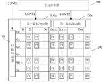
- FIG. 1 is a block diagram of a display device in accordance with an embodiment of the present invention.
- FIG. 2 is a block diagram of a signal controller in accordance with an embodiment of the present invention.
- FIG. 3 is a flow chart of a method of displaying a split screen of a display device in accordance with an embodiment of the present invention.
- FIG. 1 is a block diagram of a display device in accordance with an embodiment of the present invention.
- a display device includes a display panel assembly 100 and a signal controller 200.
- the display panel assembly 100 comprising: a plurality of pixels arranged in an array PX, N scan lines G 1 to G N, M data lines D 1 to D M, a scan driver 110, a first data driver 120a and the second data driver 120b .
- N scan lines G 1 to G N N scan lines
- M data lines D 1 to D M M data lines
- a scan driver 110 a first data driver 120a and the second data driver 120b .
- two data drivers are shown, but the present invention is not limited thereto, and for example, in a higher resolution display device, three or more data drivers may be included.
- Each pixel PX is connected to a corresponding scan line and a corresponding data line.
- Each of the pixels PX may include a switching device (not shown) connected to a corresponding scan line and a corresponding data line; and a light emitting unit (not shown) connected to the switching device.
- the switching device may preferably be a thin film transistor, but the invention is not limited thereto.
- the light emitting unit may be, for example, a liquid crystal light emitting unit or an organic light emitting unit.
- the scan driver 110 is connected to the scan lines G 1 to G N, G 1 is applied to a scanning signal to the scanning line G N, the scan signal is typically a combination of a high level signal and low level signal from.
- the first data driver 120a is connected to the data lines D 1 to D M/2 and applies a data voltage to the data lines D 1 to D M/2 ;
- the second data driver 120b is connected to the data line D (M+2)/2 to D M and apply a data voltage to data lines D (M+2)/2 to D M .
- the scan driver 110, the first data driver 120a, and the second data driver 120b are integrated and included in the liquid crystal panel assembly 100.
- the scan driver 110, the first data driver 120a, and the second data driver 120b may be mounted on a flexible printed film (not shown) and then attached to the liquid crystal panel assembly 100 (at this time, the liquid crystal panel assembly 100 does not include The scan driver 110, the first data driver 120a, and the second data driver 120b).
- the signal controller 200 controls the operations of the scan driver 110, the first data driver 120a, and the second data driver 120b.
- the signal controller 200 is capable of generating a scan control signal CONT1 and a data control signal CONT2.
- the signal controller 200 transmits the scan control signal CONT1 to the scan driver 110 and transmits the data control signal CONT2 to the first data driver 120a and the second data driver 120b, respectively.
- the first data driver 120a and the second data driver 120b CONT2 and generating a data voltage according to the code stored in each gamma are responsive to the data control signal, respectively, and applying a data voltage to the data lines D 1 to D M / 2 And data line D (M+2)/2 to D M .
- the scan driver 110 in response to a high level signal is applied to the scanning signal to the scan lines G 1 to G N of the scan control signal CONT1 turned connected to the scan lines G 1 to G N of the switching device. Then, data voltages respectively applied to the data lines D 1 to D M/2 and the data lines D (M+2)/2 to D M are transmitted to each of the pixels PX through the turned-on switching devices.
- the data voltages respectively output by the first data driver 120a and the second data driver 120b are different, thereby causing the display device to generate a display.
- the split screen phenomenon is most apparent when the display screen is displayed between the data line D M/2 to which the first data driver 120a is connected and the data line D (M+2)/2 to which the second data driver 120b is connected.
- the plurality of pixels PX display a monochrome screen of the same gray level
- the signal controller 200 acquires the data line D i connected to the first data driver 120a and the data line D j connected to the second data driver 120b.
- Voltage data on, and the signal controller 200 adjusts the gamma codes in the first data driver 120a and the second data driver 120b according to the acquired voltage data until the first data driver 120a outputs to the data line D i
- the data voltage is the same as the data voltage outputted to the data line Dj by the second data driver 120b, where 1 ⁇ i ⁇ M/2, (M + 2)/2 ⁇ j ⁇ M.
- the display screen is on the data line D M/2 and the data.
- the split screen phenomenon is most obvious between the lines D (M+2)/2 .
- the plurality of pixels PX display a monochrome picture of the same gray level, and the signal controller 200 can obtain the first picture.
- the data line D M/2 connected to the data driver 120a and the voltage data on the data line D (M+2)/2 connected to the second data driver 120b, and the signal controller 200 pairs the first data driver according to the acquired voltage data.
- the gamma code in the 120a and second data drivers 120b is adjusted until the data voltage output by the first data driver 120a to the data line D M/2 and the second data driver 120b are output to the data line D (M+2) / The data voltage on 2 is the same.
- the signal controller 200 writes the adjusted gamma code into the first data driver 120a and the second data driver 120b, respectively.
- FIG. 2 is a block diagram of a signal controller in accordance with an embodiment of the present invention.
- a signal controller 200 includes a voltage detection conversion module 210, a control module 220, and a write module 230.
- the voltage detection conversion module 210 may be an analog to digital converter (DAC), but the invention is not limited thereto.
- DAC analog to digital converter
- the voltage detection conversion module 210 detects the first data voltage on the data line D i connected to the first data driver 120a and the data line D connected to the second data driver 120b.
- the second data voltage on j converts the first data voltage and the second data voltage into a first digital signal and a second digital signal (i.e., voltage data), respectively.
- the voltage detection conversion module 210 delivers the first digital signal and the second digital signal to the control module 220.
- the control module 220 compares the difference between the first digital signal and the second digital signal, and adjusts the gamma code in the first data driver 120a and the second data driver 120b according to the difference result until the first data driver 120a outputs to the data line D.
- the data voltage on i is the same as the data voltage outputted to the data line Dj by the second data driver 120b.
- the control module 220 may adjust the gamma code in the second data driver 120b with reference to the gamma code in the first data driver 120a; or the control module 220 may be based on the gamma code in the second data driver 120b.
- the gamma code in the first data driver 120a is adjusted; or the control module 220 adjusts the gamma code in the first data driver 120a and the second data driver 120b, respectively, based on a predetermined gamma code.
- the control module 220 delivers the adjusted gamma code to the write module 230.
- the write module 230 writes the adjusted gamma code into the first data driver 120a and the second data driver 120b.
- FIG. 3 is a flow chart of a method of displaying a split screen of a display device in accordance with an embodiment of the present invention.
- a method for displaying a split screen of a display device includes the following steps:
- S310 Simultaneously display a monochrome picture of the same gray level by using a plurality of pixels PX.
- S320 Acquire voltage data on the data line D i connected by the first data driver 120a and the data line D j connected to the second data driver 120b by using the signal controller 200.
- the specific method of implementing step S320 includes: first, detecting, by the voltage detection conversion module 210 of the signal controller 200, the first data voltage and the second data driver 120b on the data line D i connected to the first data driver 120a. a second data voltage on the connected data line D j ; then, the voltage detection conversion module 210 of the signal controller 200 converts the first data voltage and the second data voltage into a first digital signal and a second digital signal, respectively (ie Voltage data).
- S330 The gamma code in the first data driver 120a and the second data driver 120b is adjusted according to the acquired voltage data by using the signal controller 200 until the data voltage and the data voltage on the data line D i are output by the first data driver 120a.
- the data voltages outputted by the second data driver 120b onto the data line Dj are the same.
- the specific method of implementing step S330 includes: first, comparing the difference between the first digital signal and the second digital signal by using the control module 220 of the signal controller 200; then, using the control module 220 of the signal controller 200 according to The difference result adjusts the gamma code in the first data driver 120a and the second data driver 120b until the data voltage outputted by the first data driver 120a to the data line D i and the second data driver 120b are output to the data line D j
- the data voltage is the same.
- control module 220 may adjust the gamma code in the second data driver 120b with reference to the gamma code in the first data driver 120a; or the control module 220 may be based on the gamma code in the second data driver 120b.
- the gamma code in the first data driver 120a is adjusted; or the control module 220 adjusts the gamma code in the first data driver 120a and the second data driver 120b, respectively, based on a predetermined gamma code.
- S340 The adjusted gamma code is written into the first data driver 120a and the second data driver 120b by the signal controller 200, respectively.
- step S340 includes writing the adjusted gamma code to the first data driver 120a and the second data driver 120b by the write module 230 of the signal controller 200, respectively.
- the above method according to the present invention can be implemented as computer code in a computer readable recording medium.
- the computer code can be implemented by those skilled in the art in accordance with the description of the above method.
- the above method of the present invention is implemented when the computer code is executed in a computer.
- each device or module in the display device may be implemented as a hardware component.
- One skilled in the art can implement various devices or modules using, for example, a field programmable gate array (FPGA) or an application specific integrated circuit (ASIC), depending on the processing performed by the various devices or modules defined.
- FPGA field programmable gate array
- ASIC application specific integrated circuit
- the display splitting phenomenon caused by the use of at least two data drivers in the high resolution display device is eliminated, thereby improving the display effect of the display device.
Landscapes
- Engineering & Computer Science (AREA)
- Physics & Mathematics (AREA)
- Computer Hardware Design (AREA)
- General Physics & Mathematics (AREA)
- Theoretical Computer Science (AREA)
- Control Of Indicators Other Than Cathode Ray Tubes (AREA)
- Liquid Crystal Display Device Control (AREA)
Abstract
一种显示装置,包括:显示面板组件(100)、信号控制器(200);显示面板组件(100)包括:阵列排布的多个像素、至少两个数据驱动器(120a,120b)以及连接到每个数据驱动器(120a,120b)上的多条数据线,像素连接到对应的数据线上;信号控制器(200)与数据驱动器(120a,120b)连接,信号控制器(200)用于当多个像素显示同灰阶的单色画面时获取相邻两个数据驱动器(120a,120b)各连接的一条数据线上的电压数据,且根据获取到的电压数据对相邻两个数据驱动器(120a,120b)中的伽马代码进行调整,直至相邻两个数据驱动器(120a,120b)输出到各连接的一条数据线上的数据电压相同。消除了高分辨率显示装置中由于使用至少两个数据驱动器(120a,120b)而引起的显示分屏现象,提高显示装置的显示效果。
Description
本发明属于显示技术领域,具体地讲,涉及一种显示装置及显示装置显示分屏的消除方法。
近年来,用户对显示装置显示效果的追求与日俱增,越来越高分辨率的显示装置广受用户的欢迎。分辨率越高,显示装置显示的图像的损失就越小。显示装置的分辨率提升的速度越来越快,然而芯片(IC)工艺的提升速度却无法追逐显示装置分辨率的提升速度,这样在高分辨率的显示装置中,往往采用两颗或者更多颗驱动芯片来进行显示驱动。
然而,在采用两颗或者更多颗驱动芯片进行显示驱动的显示装置中,由于驱动芯片在制程时产生的差异,这些驱动芯片各自输出的电压不同,从而使显示装置产生显示分屏现象。
发明内容
为了解决上述的技术问题,本发明的目的在于提供一种能够消除分屏显示现象的显示装置及显示装置显示分屏的消除方法。
根据本发明的一方面,提供了一种显示装置,其包括:显示面板组件、信号控制器;所述显示面板组件包括:阵列排布的多个像素、至少两个数据驱动器以及连接到每个数据驱动器上的多条数据线,所述像素连接到对应的数据线上;所述信号控制器与所述数据驱动器连接,所述信号控制器用于当所述多个像素显示同灰阶的单色画面时获取相邻两个数据驱动器各连接的一条数据线上的电压数据,且根据获取到的电压数据对所述相邻两个数据驱动器中的伽马代码进行调整,直至所述相邻两个数据驱动器输出到各连接的一条数据线上的数据电压相同。
进一步地,所述相邻两个数据驱动器各连接的一条数据线彼此相邻。
进一步地,所述信号控制器包括:电压检测转换模块,用于当所述多个像素显示同灰阶的单色画面时检测所述相邻两个数据驱动器各连接的一条数据线上的数据电压,并将检测到的数据电压转换为数字信号;控制模块,用于根据所述数字信号调整所述相邻两个数据驱动器中的伽马代码,直至所述相邻两个数据驱动器输出到各连接的一条数据线上的数据电压相同。
进一步地,所述信号控制器还包括:写入模块,用于将调整后的伽马代码分别写入所述相邻两个数据驱动器中。
进一步地,所述电压检测转换模块为模数转换器。
进一步地,每个数据驱动器连接的数据线的数量相同。
根据本发明的另一方面,还提供了一种显示装置显示分屏的消除方法,其包括步骤:利用多个像素显示同灰阶的单色画面;利用信号控制器获取相邻两个数据驱动器各连接的一条数据线上的电压数据;利用信号控制器根据获取到的电压数据对所述相邻两个数据驱动器中的伽马代码进行调整,直至所述相邻两个数据驱动器输出到各连接的一条数据线上的数据电压相同。
进一步地,所述相邻两个数据驱动器各连接的一条数据线彼此相邻;
进一步地,实现步骤“利用信号控制器获取相邻两个数据驱动器各连接的一条数据线上的电压数据”的方法包括:利用信号控制器获取相邻两个数据驱动器各连接的一条数据线上的数据电压;利用信号控制器将获取到的数据电压转换为数字信号。
进一步地,实现步骤“利用信号控制器根据获取到的电压数据对所述相邻两个数据驱动器中的伽马代码进行调整”的方法包括:利用信号控制器比对所述数字信号的差异;利用信号控制器根据比对结果调整所述相邻两个数据驱动器中的伽马代码。
进一步地,在步骤“利用信号控制器根据获取到的电压数据对所述相邻两个数据驱动器中的伽马代码进行调整,直至所述相邻两个数据驱动器输出到各
连接的一条数据线上的数据电压相同”之后,所述显示分屏消除方法还包括步骤:利用信号控制器将调整后的伽马代码分别写入所述相邻两个数据驱动器中。
进一步地,每个数据驱动器连接的数据线的数量相同。
本发明的有益效果:本发明消除了高分辨率显示装置中由于使用至少两个数据驱动器而引起的显示分屏现象,从而提高显示装置的显示效果。
通过结合附图进行的以下描述,本发明的实施例的上述和其它方面、特点和优点将变得更加清楚,附图中:
图1是根据本发明的实施例的显示装置的架构图;
图2是根据本发明的实施例的信号控制器的模块图;
图3是根据本发明的实施例的显示装置显示分屏的消除方法的流程图。
以下,将参照附图来详细描述本发明的实施例。然而,可以以许多不同的形式来实施本发明,并且本发明不应该被解释为限制于这里阐述的具体实施例。相反,提供这些实施例是为了解释本发明的原理及其实际应用,从而使本领域的其他技术人员能够理解本发明的各种实施例和适合于特定预期应用的各种修改。
图1是根据本发明的实施例的显示装置的架构图。
参照图1,根据本发明的实施例的显示装置包括:显示面板组件100和信号控制器200。
显示面板组件100包括:阵列排布的多个像素PX、N条扫描线G1至GN、M条数据线D1至DM、扫描驱动器110、第一数据驱动器120a和第二数据驱动器120b。在本实施例中,示出了两个数据驱动器,但本发明并不限制于此,例如在更高分辨了的显示装置中,可以包括三个或者更多个数据驱动器。
每个像素PX连接到对应的扫描线和对应的数据线。每个像素PX可以包括:开关器件(未示出),连接到对应的扫描线和对应的数据线;发光单元(未示出),连接到该开关器件。在本实施例中,该开关器件可优选为薄膜晶体管,但本发明并不限制于此。发光单元可例如是液晶发光单元或者有机发光单元。
扫描驱动器110连接到扫描线G1至GN,并向扫描线G1至GN施加扫描信号,该扫描信号通常由高电平信号和低电平信号组合而成。
第一数据驱动器120a连接到数据线D1至DM/2,并向数据线D1至DM/2施加数据电压;第二数据驱动器120b连接到数据线D(M+2)/2至DM,并向数据线D(M+2)/2至DM施加数据电压。
在本实施例中,扫描驱动器110、第一数据驱动器120a和第二数据驱动器120b被集成而包括于液晶面板组件100中。可替换地,扫描驱动器110、第一数据驱动器120a和第二数据驱动器120b可以被安装在柔性印刷薄膜(未示出)上,然后附接到液晶面板组件100(此时液晶面板组件100不包含扫描驱动器110、第一数据驱动器120a和第二数据驱动器120b)。
信号控制器200控制扫描驱动器110、第一数据驱动器120a和第二数据驱动器120b的操作。
信号控制器200能够产生扫描控制信号CONT1和数据控制信号CONT2。信号控制器200将扫描控制信号CONT1传送到扫描驱动器110,并将数据控制信号CONT2分别传送到第一数据驱动器120a和第二数据驱动器120b。
第一数据驱动器120a和第二数据驱动器120b分别响应于数据控制信号CONT2并根据各自存储的伽马代码(Gamma Code)产生数据电压,并分别将数据电压施加到数据线D1至DM/2和数据线D(M+2)/2至DM。
扫描驱动器110响应于扫描控制信号CONT1向扫描线G1至GN施加为高电平信号的扫描信号而导通连接到扫描线G1至GN的开关器件。然后,分别施加到数据线D1至DM/2和数据线D(M+2)/2至DM的数据电压通过导通的开关器件而被传送到每个像素PX。
诚如背景技术中描述,由于第一数据驱动器120a和第二数据驱动器120b
在制程时产生的差异,第一数据驱动器120a和第二数据驱动器120b各自输出的数据电压不同,从而使显示装置产生显示分屏现象,而显示画面在第一数据驱动器120a连接的数据线DM/2和第二数据驱动器120b连接的数据线D(M+2)/2之间出现显示分屏现象最明显。
为了消除上述显示分屏现象,使多个像素PX显示同灰阶的单色画面,信号控制器200获取第一数据驱动器120a连接的数据线Di和第二数据驱动器120b连接的数据线Dj上的电压数据,并且信号控制器200根据获取到的电压数据对第一数据驱动器120a和第二数据驱动器120b中的伽马代码进行调整,直至第一数据驱动器120a输出至数据线Di上的数据电压和第二数据驱动器120b输出至数据线Dj上的数据电压相同,其中,1≤i≤M/2,(M+2)/2≤j≤M。
优选地,由于连接第一数据驱动器120a的数据线DM/2和连接第二数据驱动器120b的数据线D(M+2)/2彼此相邻,显示画面在数据线DM/2和数据线D(M+2)/2之间出现分屏现象最明显,为了更有效地消除上述分屏现象,使多个像素PX显示同灰阶的单色画面,信号控制器200可获取第一数据驱动器120a连接的数据线DM/2和第二数据驱动器120b连接的数据线D(M+2)/2上的电压数据,并且信号控制器200根据获取到的电压数据对第一数据驱动器120a和第二数据驱动器120b中的伽马代码进行调整,直至第一数据驱动器120a输出至数据线DM/2上的数据电压和第二数据驱动器120b输出至数据线D(M+2)/2上的数据电压相同。
进一步地,信号控制器200将调整后的伽马代码分别写入第一数据驱动器120a和第二数据驱动器120b中。
图2是根据本发明的实施例的信号控制器的模块图。
参照图2,根据本发明的实施例的信号控制器200包括:电压检测转换模块210、控制模块220以及写入模块230。
优选地,电压检测转换模块210可为模数转换器(DAC),但本发明并不限制于此。当多个像素PX同时显示同灰阶的单色画面时,电压检测转换模块210检测第一数据驱动器120a连接的数据线Di上的第一数据电压和第二数据驱动器120b连接的数据线Dj上的第二数据电压,并将第一数据电压和第二数
据电压分别转换为第一数字信号和第二数字信号(即电压数据)。
电压检测转换模块210将第一数字信号和第二数字信号输送至控制模块220。控制模块220比对第一数字信号和第二数字信号的差异,并根据差异结果调整第一数据驱动器120a和第二数据驱动器120b中的伽马代码,直至第一数据驱动器120a输出至数据线Di上的数据电压和第二数据驱动器120b输出至数据线Dj上的数据电压相同。这里,控制模块220可以以第一数据驱动器120a中的伽马代码为基准,调整第二数据驱动器120b中的伽马代码;或者控制模块220可以以第二数据驱动器120b中的伽马代码为基准,调整第一数据驱动器120a中的伽马代码;或者控制模块220以一预定的伽马代码为基准,分别调整第一数据驱动器120a和第二数据驱动器120b中的伽马代码。
控制模块220将调整后的伽马代码输送至写入模块230。写入模块230将调整后的伽马代码写入第一数据驱动器120a和第二数据驱动器120b中。
图3是根据本发明的实施例的显示装置显示分屏的消除方法的流程图。
参照图1和图3,根据本发明的实施例的显示装置显示分屏的消除方法包括以下步骤:
S310:利用多个像素PX同时显示同灰阶的单色画面。
S320:利用信号控制器200获取第一数据驱动器120a连接的数据线Di和第二数据驱动器120b连接的数据线Dj上的电压数据。
结合参照图2,实现步骤S320的具体方法包括:首先,利用信号控制器200的电压检测转换模块210检测第一数据驱动器120a连接的数据线Di上的第一数据电压和第二数据驱动器120b连接的数据线Dj上的第二数据电压;接着,利用信号控制器200的电压检测转换模块210将第一数据电压和第二数据电压分别转换为第一数字信号和第二数字信号(即电压数据)。
S330:利用信号控制器200根据获取到的电压数据对第一数据驱动器120a和第二数据驱动器120b中的伽马代码进行调整,直至第一数据驱动器120a输出至数据线Di上的数据电压和第二数据驱动器120b输出至数据线Dj上的数据电压相同。
结合参照图2,实现步骤S330的具体方法包括:首先,利用信号控制器200的控制模块220比对第一数字信号和第二数字信号的差异;接着,利用信号控制器200的控制模块220根据差异结果调整第一数据驱动器120a和第二数据驱动器120b中的伽马代码,直至第一数据驱动器120a输出至数据线Di上的数据电压和第二数据驱动器120b输出至数据线Dj上的数据电压相同。
这里,控制模块220可以以第一数据驱动器120a中的伽马代码为基准,调整第二数据驱动器120b中的伽马代码;或者控制模块220可以以第二数据驱动器120b中的伽马代码为基准,调整第一数据驱动器120a中的伽马代码;或者控制模块220以一预定的伽马代码为基准,分别调整第一数据驱动器120a和第二数据驱动器120b中的伽马代码。
S340:利用信号控制器200将调整后的伽马代码分别写入第一数据驱动器120a和第二数据驱动器120b中。
结合参照图2,实现步骤S340的具体方法包括:利用信号控制器200的写入模块230将调整后的伽马代码分别写入第一数据驱动器120a和第二数据驱动器120b中。
此外,根据本发明的上述方法可以被实现为计算机可读记录介质中的计算机代码。本领域技术人员可以根据对上述方法的描述来实现所述计算机代码。当所述计算机代码在计算机中被执行时实现本发明的上述方法。
此外,根据本发明的实施例的显示装置中的各个器件或模块可被实现为硬件组件。本领域技术人员根据限定的各个器件或模块所执行的处理,可以使用例如现场可编程门阵列(FPGA)或专用集成电路(ASIC)来实现各个器件或模块。
综上所述,根据本发明的实施例,消除了高分辨率显示装置中由于使用至少两个数据驱动器而引起的显示分屏现象,从而提高显示装置的显示效果。
虽然已经参照特定实施例示出并描述了本发明,但是本领域的技术人员将理解:在不脱离由权利要求及其等同物限定的本发明的精神和范围的情况下,可在此进行形式和细节上的各种变化。
Claims (16)
- 一种显示装置,其中,包括:显示面板组件、信号控制器;所述显示面板组件包括:阵列排布的多个像素、至少两个数据驱动器以及连接到每个数据驱动器上的多条数据线,所述像素连接到对应的数据线上;所述信号控制器与所述数据驱动器连接,所述信号控制器用于当所述多个像素显示同灰阶的单色画面时获取相邻两个数据驱动器各连接的一条数据线上的电压数据,且根据获取到的电压数据对所述相邻两个数据驱动器中的伽马代码进行调整,直至所述相邻两个数据驱动器输出到各连接的一条数据线上的数据电压相同。
- 根据权利要求1所述的显示装置,其中,所述相邻两个数据驱动器各连接的一条数据线彼此相邻。
- 根据权利要求1所述的显示装置,其中,所述信号控制器包括:电压检测转换模块,用于当所述多个像素显示同灰阶的单色画面时检测所述相邻两个数据驱动器各连接的一条数据线上的数据电压,并将检测到的数据电压转换为数字信号;控制模块,用于根据所述数字信号调整所述相邻两个数据驱动器中的伽马代码,直至所述相邻两个数据驱动器输出到各连接的一条数据线上的数据电压相同。
- 根据权利要求2所述的显示装置,其中,所述信号控制器包括:电压检测转换模块,用于当所述多个像素显示同灰阶的单色画面时检测所述相邻两个数据驱动器各连接的一条数据线上的数据电压,并将检测到的数据电压转换为数字信号;控制模块,用于根据所述数字信号调整所述相邻两个数据驱动器中的伽马代码,直至所述相邻两个数据驱动器输出到各连接的一条数据线上的数据电压 相同。
- 根据权利要求3所述的显示装置,其中,所述信号控制器还包括:写入模块,用于将调整后的伽马代码分别写入所述相邻两个数据驱动器中。
- 根据权利要求4所述的显示装置,其中,所述信号控制器还包括:写入模块,用于将调整后的伽马代码分别写入所述相邻两个数据驱动器中。
- 根据权利要求3所述的显示装置,其中,所述电压检测转换模块为模数转换器。
- 根据权利要求4所述的显示装置,其中,所述电压检测转换模块为模数转换器。
- 一种显示装置显示分屏的消除方法,其中,包括步骤:利用多个像素显示同灰阶的单色画面;利用信号控制器获取相邻两个数据驱动器各连接的一条数据线上的电压数据;利用信号控制器根据获取到的电压数据对所述相邻两个数据驱动器中的伽马代码进行调整,直至所述相邻两个数据驱动器输出到各连接的一条数据线上的数据电压相同。
- 根据权利要求9所述的消除方法,其中,所述相邻两个数据驱动器各连接的一条数据线彼此相邻。
- 根据权利要求9所述的消除方法,其中,实现步骤“利用信号控制器获取相邻两个数据驱动器各连接的一条数据线上的电压数据”的方法包括:利用信号控制器获取相邻两个数据驱动器各连接的一条数据线上的数据电压;利用信号控制器将获取到的数据电压转换为数字信号。
- 根据权利要求10所述的消除方法,其中,实现步骤“利用信号控制器获取相邻两个数据驱动器各连接的一条数据线上的电压数据”的方法包括:利用信号控制器获取相邻两个数据驱动器各连接的一条数据线上的数据电压;利用信号控制器将获取到的数据电压转换为数字信号。
- 根据权利要求11所述的消除方法,其中,实现步骤“利用信号控制器根据获取到的电压数据对所述相邻两个数据驱动器中的伽马代码进行调整”的方法包括:利用信号控制器比对所述数字信号的差异;利用信号控制器根据比对结果调整所述相邻两个数据驱动器中的伽马代码。
- 根据权利要求12所述的消除方法,其中,实现步骤“利用信号控制器根据获取到的电压数据对所述相邻两个数据驱动器中的伽马代码进行调整”的方法包括:利用信号控制器比对所述数字信号的差异;利用信号控制器根据比对结果调整所述相邻两个数据驱动器中的伽马代码。
- 根据权利要求9所述的消除方法,其中,在步骤“利用信号控制器根据获取到的电压数据对所述相邻两个数据驱动器中的伽马代码进行调整,直至所述相邻两个数据驱动器输出到各连接的一条数据线上的数据电压相同”之后,所述显示分屏消除方法还包括步骤:利用信号控制器将调整后的伽马代码分别写入所述相邻两个数据驱动器中。
- 根据权利要求10所述的消除方法,其中,在步骤“利用信号控制器 根据获取到的电压数据对所述相邻两个数据驱动器中的伽马代码进行调整,直至所述相邻两个数据驱动器输出到各连接的一条数据线上的数据电压相同”之后,所述显示分屏消除方法还包括步骤:利用信号控制器将调整后的伽马代码分别写入所述相邻两个数据驱动器中。
Priority Applications (1)
| Application Number | Priority Date | Filing Date | Title |
|---|---|---|---|
| US15/328,592 US10235922B2 (en) | 2016-12-27 | 2016-12-29 | Display devices and methods of eliminating split screen for display devices |
Applications Claiming Priority (2)
| Application Number | Priority Date | Filing Date | Title |
|---|---|---|---|
| CN201611226988.9A CN106782265B (zh) | 2016-12-27 | 2016-12-27 | 显示装置及显示装置显示分屏的消除方法 |
| CN201611226988.9 | 2016-12-27 |
Related Child Applications (1)
| Application Number | Title | Priority Date | Filing Date |
|---|---|---|---|
| US16/436,086 Continuation US11175668B2 (en) | 2016-12-30 | 2019-06-10 | Navigation method and apparatus, and terminal device |
Publications (1)
| Publication Number | Publication Date |
|---|---|
| WO2018119948A1 true WO2018119948A1 (zh) | 2018-07-05 |
Family
ID=58922062
Family Applications (1)
| Application Number | Title | Priority Date | Filing Date |
|---|---|---|---|
| PCT/CN2016/113256 Ceased WO2018119948A1 (zh) | 2016-12-27 | 2016-12-29 | 显示装置及显示装置显示分屏的消除方法 |
Country Status (3)
| Country | Link |
|---|---|
| US (1) | US10235922B2 (zh) |
| CN (1) | CN106782265B (zh) |
| WO (1) | WO2018119948A1 (zh) |
Families Citing this family (11)
| Publication number | Priority date | Publication date | Assignee | Title |
|---|---|---|---|---|
| CN106875896B (zh) * | 2017-04-28 | 2019-04-05 | 京东方科技集团股份有限公司 | 一种源极驱动ic、显示装置及其驱动方法 |
| CN107290903B (zh) * | 2017-07-28 | 2020-08-07 | 武汉天马微电子有限公司 | 一种阵列基板、显示面板和显示装置 |
| CN108735141A (zh) * | 2018-07-27 | 2018-11-02 | 武汉华星光电技术有限公司 | 驱动电路 |
| US10861377B2 (en) | 2018-10-24 | 2020-12-08 | HKC Corporation Limited | Gamma voltage correction circuit, method and display device |
| CN109243355B (zh) * | 2018-10-24 | 2021-04-06 | 惠科股份有限公司 | 伽马电压校正电路、方法及显示装置 |
| US11783739B2 (en) * | 2020-09-10 | 2023-10-10 | Apple Inc. | On-chip testing architecture for display system |
| US11645957B1 (en) * | 2020-09-10 | 2023-05-09 | Apple Inc. | Defective display source driver screening and repair |
| CN112669783B (zh) | 2020-12-29 | 2023-01-10 | Tcl华星光电技术有限公司 | 一种数据信号调节电路和显示装置 |
| CN113284467B (zh) * | 2021-05-18 | 2022-09-09 | 京东方科技集团股份有限公司 | 源极驱动器及其伽马电压补偿方法、显示模组、显示装置 |
| CN115565487B (zh) * | 2022-09-28 | 2025-09-19 | 京东方科技集团股份有限公司 | 源极芯片的电压配置方法、装置及电子设备 |
| KR20250132676A (ko) * | 2024-02-29 | 2025-09-05 | 엘지디스플레이 주식회사 | 표시 장치 |
Citations (8)
| Publication number | Priority date | Publication date | Assignee | Title |
|---|---|---|---|---|
| US6429841B1 (en) * | 1998-08-11 | 2002-08-06 | Lg. Philips Lcd Co., Ltd. | Active matrix liquid crystal display apparatus and method for flicker compensation |
| US20050128113A1 (en) * | 2003-12-12 | 2005-06-16 | Samsung Electronics Co., Ltd. | Gamma correction D/A converter, source driver integrated circuit and display having the same and D/A converting method using gamma correction |
| CN101110187A (zh) * | 2006-07-20 | 2008-01-23 | 晶门科技有限公司 | 在显示系统中提高列线输出的均匀性的驱动电路、系统以及方法 |
| CN101482664A (zh) * | 2008-01-10 | 2009-07-15 | 精工爱普生株式会社 | 电光装置、电光装置的驱动方法、电子设备 |
| CN103117049A (zh) * | 2013-01-29 | 2013-05-22 | 南京中电熊猫液晶显示科技有限公司 | 一种改善灰阶细纹的驱动方法 |
| CN103903582A (zh) * | 2012-12-26 | 2014-07-02 | 乐金显示有限公司 | 液晶显示器及其制造方法 |
| CN104751762A (zh) * | 2013-12-31 | 2015-07-01 | 乐金显示有限公司 | 显示设备及其驱动方法 |
| CN105741783A (zh) * | 2014-12-24 | 2016-07-06 | 乐金显示有限公司 | 显示装置及其驱动方法 |
-
2016
- 2016-12-27 CN CN201611226988.9A patent/CN106782265B/zh active Active
- 2016-12-29 US US15/328,592 patent/US10235922B2/en active Active
- 2016-12-29 WO PCT/CN2016/113256 patent/WO2018119948A1/zh not_active Ceased
Patent Citations (8)
| Publication number | Priority date | Publication date | Assignee | Title |
|---|---|---|---|---|
| US6429841B1 (en) * | 1998-08-11 | 2002-08-06 | Lg. Philips Lcd Co., Ltd. | Active matrix liquid crystal display apparatus and method for flicker compensation |
| US20050128113A1 (en) * | 2003-12-12 | 2005-06-16 | Samsung Electronics Co., Ltd. | Gamma correction D/A converter, source driver integrated circuit and display having the same and D/A converting method using gamma correction |
| CN101110187A (zh) * | 2006-07-20 | 2008-01-23 | 晶门科技有限公司 | 在显示系统中提高列线输出的均匀性的驱动电路、系统以及方法 |
| CN101482664A (zh) * | 2008-01-10 | 2009-07-15 | 精工爱普生株式会社 | 电光装置、电光装置的驱动方法、电子设备 |
| CN103903582A (zh) * | 2012-12-26 | 2014-07-02 | 乐金显示有限公司 | 液晶显示器及其制造方法 |
| CN103117049A (zh) * | 2013-01-29 | 2013-05-22 | 南京中电熊猫液晶显示科技有限公司 | 一种改善灰阶细纹的驱动方法 |
| CN104751762A (zh) * | 2013-12-31 | 2015-07-01 | 乐金显示有限公司 | 显示设备及其驱动方法 |
| CN105741783A (zh) * | 2014-12-24 | 2016-07-06 | 乐金显示有限公司 | 显示装置及其驱动方法 |
Also Published As
| Publication number | Publication date |
|---|---|
| US20180211581A1 (en) | 2018-07-26 |
| CN106782265A (zh) | 2017-05-31 |
| US10235922B2 (en) | 2019-03-19 |
| CN106782265B (zh) | 2019-01-11 |
Similar Documents
| Publication | Publication Date | Title |
|---|---|---|
| WO2018119948A1 (zh) | 显示装置及显示装置显示分屏的消除方法 | |
| US7893912B2 (en) | Timing controller for liquid crystal display | |
| US9830861B2 (en) | Display device | |
| US10152908B2 (en) | Timing controller, display device, and method of driving the same | |
| US9311839B2 (en) | Method for driving liquid crystal panel, method for testing flicker and liquid crystal display apparatus | |
| CN104732944B (zh) | 源极驱动电路、源极驱动方法及显示装置 | |
| CN109949769B (zh) | 能够灰度扩展的显示装置 | |
| KR102219091B1 (ko) | 표시장치 | |
| US9847053B2 (en) | Display apparatus, gate driver and operation method thereof | |
| US20160005358A1 (en) | Driving method, driving apparatus, and organic light emitting display | |
| CN112216239B (zh) | 源极驱动器和显示装置 | |
| KR20100081760A (ko) | 표시 장치 및 표시 장치의 구동 회로 | |
| US20200057491A1 (en) | Display system, driver integrated circuit applied to the display system, and associated method | |
| US10242638B2 (en) | Display adjusting device, power source circuit, display device and display adjusting method | |
| KR20150078838A (ko) | 얼룩 보상 방법과 이를 이용한 표시장치 | |
| WO2020194493A1 (ja) | 表示装置 | |
| WO2018116337A1 (ja) | ムラ補正システム、ムラ補正装置及びパネル駆動回路 | |
| JP2012189767A (ja) | 液晶表示装置 | |
| KR20070099170A (ko) | 데이터 변환장치 및 변환방법과 이를 이용한 영상표시장치의 구동장치 및 구동방법 | |
| TW201312529A (zh) | 顯示器、時序控制器及其操作方法 | |
| CN102201191B (zh) | 显示装置 | |
| KR101427591B1 (ko) | 데이터 구동회로, 이를 포함하는 디스플레이장치 및 그제어방법 | |
| KR102881827B1 (ko) | 디스플레이 장치, 디스플레이 신호의 노이즈 검출 회로, 및 노이즈 검출 방법 | |
| KR20150098941A (ko) | 고화질 구현용 화질 보상 시스템 | |
| KR102270603B1 (ko) | 액정표시장치 |
Legal Events
| Date | Code | Title | Description |
|---|---|---|---|
| WWE | Wipo information: entry into national phase |
Ref document number: 15328592 Country of ref document: US |
|
| 121 | Ep: the epo has been informed by wipo that ep was designated in this application |
Ref document number: 16925072 Country of ref document: EP Kind code of ref document: A1 |
|
| NENP | Non-entry into the national phase |
Ref country code: DE |
|
| 122 | Ep: pct application non-entry in european phase |
Ref document number: 16925072 Country of ref document: EP Kind code of ref document: A1 |