WO2018110258A1 - Solid-state image pickup element - Google Patents
Solid-state image pickup element Download PDFInfo
- Publication number
- WO2018110258A1 WO2018110258A1 PCT/JP2017/042400 JP2017042400W WO2018110258A1 WO 2018110258 A1 WO2018110258 A1 WO 2018110258A1 JP 2017042400 W JP2017042400 W JP 2017042400W WO 2018110258 A1 WO2018110258 A1 WO 2018110258A1
- Authority
- WO
- WIPO (PCT)
- Prior art keywords
- charge holding
- solid
- light receiving
- unit
- imaging device
- Prior art date
Links
- 238000003384 imaging method Methods 0.000 claims description 60
- 239000012535 impurity Substances 0.000 claims description 42
- 239000000758 substrate Substances 0.000 claims description 32
- 239000004065 semiconductor Substances 0.000 claims description 30
- 238000006243 chemical reaction Methods 0.000 claims description 20
- 230000000903 blocking effect Effects 0.000 abstract 3
- 230000003071 parasitic effect Effects 0.000 description 21
- 238000000034 method Methods 0.000 description 16
- 238000010586 diagram Methods 0.000 description 15
- 206010047571 Visual impairment Diseases 0.000 description 14
- 238000005421 electrostatic potential Methods 0.000 description 11
- 230000004048 modification Effects 0.000 description 8
- 238000012986 modification Methods 0.000 description 8
- 238000005259 measurement Methods 0.000 description 7
- 230000003287 optical effect Effects 0.000 description 7
- 102100036285 25-hydroxyvitamin D-1 alpha hydroxylase, mitochondrial Human genes 0.000 description 6
- 101000875403 Homo sapiens 25-hydroxyvitamin D-1 alpha hydroxylase, mitochondrial Proteins 0.000 description 6
- 230000000694 effects Effects 0.000 description 6
- 229910052751 metal Inorganic materials 0.000 description 4
- 239000002184 metal Substances 0.000 description 4
- 238000009825 accumulation Methods 0.000 description 3
- 230000007423 decrease Effects 0.000 description 3
- 238000004519 manufacturing process Methods 0.000 description 3
- 150000002500 ions Chemical class 0.000 description 2
- 238000002955 isolation Methods 0.000 description 2
- 239000011159 matrix material Substances 0.000 description 2
- WFKWXMTUELFFGS-UHFFFAOYSA-N tungsten Chemical compound [W] WFKWXMTUELFFGS-UHFFFAOYSA-N 0.000 description 2
- 229910052721 tungsten Inorganic materials 0.000 description 2
- 239000010937 tungsten Substances 0.000 description 2
- VYPSYNLAJGMNEJ-UHFFFAOYSA-N Silicium dioxide Chemical compound O=[Si]=O VYPSYNLAJGMNEJ-UHFFFAOYSA-N 0.000 description 1
- XUIMIQQOPSSXEZ-UHFFFAOYSA-N Silicon Chemical compound [Si] XUIMIQQOPSSXEZ-UHFFFAOYSA-N 0.000 description 1
- 230000003247 decreasing effect Effects 0.000 description 1
- 238000009792 diffusion process Methods 0.000 description 1
- 238000005516 engineering process Methods 0.000 description 1
- 238000005468 ion implantation Methods 0.000 description 1
- 230000001678 irradiating effect Effects 0.000 description 1
- 239000000463 material Substances 0.000 description 1
- 229910021420 polycrystalline silicon Inorganic materials 0.000 description 1
- 229920005591 polysilicon Polymers 0.000 description 1
- 238000005096 rolling process Methods 0.000 description 1
- 230000035945 sensitivity Effects 0.000 description 1
- 229910052710 silicon Inorganic materials 0.000 description 1
- 239000010703 silicon Substances 0.000 description 1
- 229910052814 silicon oxide Inorganic materials 0.000 description 1
- 238000004544 sputter deposition Methods 0.000 description 1
- 230000001629 suppression Effects 0.000 description 1
- 238000010408 sweeping Methods 0.000 description 1
Images


Classifications
-
- H—ELECTRICITY
- H01—ELECTRIC ELEMENTS
- H01L—SEMICONDUCTOR DEVICES NOT COVERED BY CLASS H10
- H01L27/00—Devices consisting of a plurality of semiconductor or other solid-state components formed in or on a common substrate
- H01L27/14—Devices consisting of a plurality of semiconductor or other solid-state components formed in or on a common substrate including semiconductor components sensitive to infrared radiation, light, electromagnetic radiation of shorter wavelength or corpuscular radiation and specially adapted either for the conversion of the energy of such radiation into electrical energy or for the control of electrical energy by such radiation
- H01L27/144—Devices controlled by radiation
- H01L27/146—Imager structures
- H01L27/14601—Structural or functional details thereof
- H01L27/14609—Pixel-elements with integrated switching, control, storage or amplification elements
- H01L27/14612—Pixel-elements with integrated switching, control, storage or amplification elements involving a transistor
-
- H—ELECTRICITY
- H04—ELECTRIC COMMUNICATION TECHNIQUE
- H04N—PICTORIAL COMMUNICATION, e.g. TELEVISION
- H04N25/00—Circuitry of solid-state image sensors [SSIS]; Control thereof
- H04N25/50—Control of the SSIS exposure
- H04N25/57—Control of the dynamic range
- H04N25/59—Control of the dynamic range by controlling the amount of charge storable in the pixel, e.g. modification of the charge conversion ratio of the floating node capacitance
-
- H—ELECTRICITY
- H01—ELECTRIC ELEMENTS
- H01L—SEMICONDUCTOR DEVICES NOT COVERED BY CLASS H10
- H01L27/00—Devices consisting of a plurality of semiconductor or other solid-state components formed in or on a common substrate
- H01L27/14—Devices consisting of a plurality of semiconductor or other solid-state components formed in or on a common substrate including semiconductor components sensitive to infrared radiation, light, electromagnetic radiation of shorter wavelength or corpuscular radiation and specially adapted either for the conversion of the energy of such radiation into electrical energy or for the control of electrical energy by such radiation
- H01L27/144—Devices controlled by radiation
- H01L27/146—Imager structures
- H01L27/14601—Structural or functional details thereof
- H01L27/14603—Special geometry or disposition of pixel-elements, address-lines or gate-electrodes
-
- H—ELECTRICITY
- H01—ELECTRIC ELEMENTS
- H01L—SEMICONDUCTOR DEVICES NOT COVERED BY CLASS H10
- H01L27/00—Devices consisting of a plurality of semiconductor or other solid-state components formed in or on a common substrate
- H01L27/14—Devices consisting of a plurality of semiconductor or other solid-state components formed in or on a common substrate including semiconductor components sensitive to infrared radiation, light, electromagnetic radiation of shorter wavelength or corpuscular radiation and specially adapted either for the conversion of the energy of such radiation into electrical energy or for the control of electrical energy by such radiation
- H01L27/144—Devices controlled by radiation
- H01L27/146—Imager structures
- H01L27/14601—Structural or functional details thereof
- H01L27/1462—Coatings
- H01L27/14623—Optical shielding
-
- H—ELECTRICITY
- H01—ELECTRIC ELEMENTS
- H01L—SEMICONDUCTOR DEVICES NOT COVERED BY CLASS H10
- H01L27/00—Devices consisting of a plurality of semiconductor or other solid-state components formed in or on a common substrate
- H01L27/14—Devices consisting of a plurality of semiconductor or other solid-state components formed in or on a common substrate including semiconductor components sensitive to infrared radiation, light, electromagnetic radiation of shorter wavelength or corpuscular radiation and specially adapted either for the conversion of the energy of such radiation into electrical energy or for the control of electrical energy by such radiation
- H01L27/144—Devices controlled by radiation
- H01L27/146—Imager structures
- H01L27/14601—Structural or functional details thereof
- H01L27/1463—Pixel isolation structures
-
- H—ELECTRICITY
- H01—ELECTRIC ELEMENTS
- H01L—SEMICONDUCTOR DEVICES NOT COVERED BY CLASS H10
- H01L27/00—Devices consisting of a plurality of semiconductor or other solid-state components formed in or on a common substrate
- H01L27/14—Devices consisting of a plurality of semiconductor or other solid-state components formed in or on a common substrate including semiconductor components sensitive to infrared radiation, light, electromagnetic radiation of shorter wavelength or corpuscular radiation and specially adapted either for the conversion of the energy of such radiation into electrical energy or for the control of electrical energy by such radiation
- H01L27/144—Devices controlled by radiation
- H01L27/146—Imager structures
- H01L27/14643—Photodiode arrays; MOS imagers
-
- H—ELECTRICITY
- H04—ELECTRIC COMMUNICATION TECHNIQUE
- H04N—PICTORIAL COMMUNICATION, e.g. TELEVISION
- H04N23/00—Cameras or camera modules comprising electronic image sensors; Control thereof
- H04N23/50—Constructional details
- H04N23/55—Optical parts specially adapted for electronic image sensors; Mounting thereof
-
- H—ELECTRICITY
- H04—ELECTRIC COMMUNICATION TECHNIQUE
- H04N—PICTORIAL COMMUNICATION, e.g. TELEVISION
- H04N25/00—Circuitry of solid-state image sensors [SSIS]; Control thereof
- H04N25/40—Extracting pixel data from image sensors by controlling scanning circuits, e.g. by modifying the number of pixels sampled or to be sampled
-
- H—ELECTRICITY
- H04—ELECTRIC COMMUNICATION TECHNIQUE
- H04N—PICTORIAL COMMUNICATION, e.g. TELEVISION
- H04N25/00—Circuitry of solid-state image sensors [SSIS]; Control thereof
- H04N25/60—Noise processing, e.g. detecting, correcting, reducing or removing noise
- H04N25/62—Detection or reduction of noise due to excess charges produced by the exposure, e.g. smear, blooming, ghost image, crosstalk or leakage between pixels
-
- H—ELECTRICITY
- H04—ELECTRIC COMMUNICATION TECHNIQUE
- H04N—PICTORIAL COMMUNICATION, e.g. TELEVISION
- H04N25/00—Circuitry of solid-state image sensors [SSIS]; Control thereof
- H04N25/70—SSIS architectures; Circuits associated therewith
-
- H—ELECTRICITY
- H04—ELECTRIC COMMUNICATION TECHNIQUE
- H04N—PICTORIAL COMMUNICATION, e.g. TELEVISION
- H04N25/00—Circuitry of solid-state image sensors [SSIS]; Control thereof
- H04N25/70—SSIS architectures; Circuits associated therewith
- H04N25/76—Addressed sensors, e.g. MOS or CMOS sensors
Definitions
- the technology described in this specification relates to a solid-state imaging device.
- a global shutter type solid-state imaging device including a charge holding unit
- photoelectric conversion is not performed in the charge holding unit even when light is incident on the pixel region during a period in which the charge is held in the charge holding unit. It is done. Therefore, for example, in order to block incident light from above, a light shielding film made of metal as exemplified in Patent Document 1 is provided above the charge holding portion.
- Patent Document 2 proposes that an insulating film embedded in a trench is provided and incident light is reflected inside the semiconductor substrate due to a difference in refractive index between the semiconductor substrate and the insulating film.
- the technique disclosed in this specification is intended to provide a solid-state imaging device capable of greatly reducing optical crosstalk.
- the solid-state imaging device disclosed in this specification includes an imaging region in which a plurality of pixels are arranged.
- a light receiving portion provided on a semiconductor substrate and generating charges by photoelectric conversion
- a charge holding portion provided on the semiconductor substrate and storing charges generated in the light receiving portion
- the charge holding portion A gate electrode provided on the light-receiving portion for transferring the charge generated in the light-receiving portion to the charge holding portion; and a first electrode formed in a region of the semiconductor substrate between the light-receiving portion and the charge holding portion.
- a first insulating film provided in the first trench, a second trench formed in a region between light receiving portions of adjacent pixels of the semiconductor substrate, and the first trench A second insulating film provided in the trench of 2 and an end of a boundary between the light receiving unit and the charge holding unit provided in contact with the first insulating film, from the light receiving unit to the charge holding unit
- a transfer section serving as a charge transfer path to the Holding portion, and a light shielding film is provided to cover the transfer unit and the gate electrode electrode.
- the distance from the end of the light shielding film to the charge holding unit across the transfer unit in the direction from the light receiving unit to the charge holding unit is the first distance from the end of the light shielding film to the first holding unit. Longer than the distance to the charge holding portion across the trench.
- optical crosstalk can be significantly reduced.
- FIG. 1 is a circuit diagram illustrating a configuration of a pixel circuit of a solid-state imaging device according to an embodiment of the present disclosure.
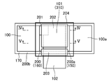
- FIG. 2 is a plan view schematically showing the solid-state imaging device according to the embodiment.
- FIG. 3 is a plan view showing a configuration of a pixel in the solid-state imaging device according to the embodiment.
- 4 is a cross-sectional view showing a cross section taken along line IV-IV of the solid-state imaging device shown in FIG.
- FIG. 5 is a cross-sectional view showing a cross section taken along line VV of the solid-state imaging device shown in FIG.
- FIG. 6A is a cross-sectional view illustrating the method for manufacturing the solid-state imaging device according to the embodiment.
- FIG. 1 is a circuit diagram illustrating a configuration of a pixel circuit of a solid-state imaging device according to an embodiment of the present disclosure.
- FIG. 2 is a plan view schematically showing the solid-state imaging device according to the embodiment.
- FIG. 6B is a cross-sectional view illustrating the method for manufacturing the solid-state imaging device according to the embodiment.
- FIG. 7 is a plan view showing a solid-state imaging device according to a first modification of the embodiment.
- FIG. 8 is a plan view showing a solid-state imaging device according to a second modification of the embodiment.
- FIG. 9 is a plan view showing a solid-state imaging device used for effect measurement.
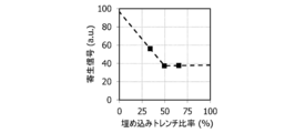
- FIG. 10A is a diagram illustrating a relationship between a buried trench ratio and a parasitic signal.
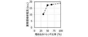
- FIG. 10B is a diagram showing the relationship between the buried trench ratio and the afterimage.
- FIG. 10C is a diagram showing the relationship between the buried trench ratio and the dark current in the accumulation region.
- FIG. 10A is a diagram illustrating a relationship between a buried trench ratio and a parasitic signal.
- FIG. 10B is a diagram showing the relationship between the buried trench ratio and the afterimage.
- FIG. 10C is a diagram showing the
- FIG. 11 is a plan view showing a solid-state imaging device used for effect measurement.
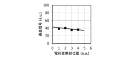
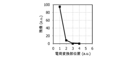
- FIG. 12 is a diagram illustrating the relationship between the position of the charge holding unit 101 and the magnitude of the parasitic signal.
- FIG. 13 is a plan view showing a solid-state imaging device used for effect measurement.
- FIG. 14A is a diagram illustrating the relationship between the position 404 of the protruding portion of the light receiving unit 100 and the parasitic signal.
- FIG. 14B is a diagram illustrating a relationship between the position 404 of the protruding portion of the light receiving unit 100 and the afterimage.
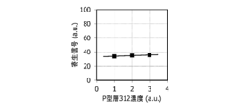
- FIG. 15A is a diagram illustrating changes in parasitic signals when the p-type impurity concentration of the p-type layer 312 of the transfer unit 201 is changed in the solid-state imaging device.
- FIG. 15B is a diagram illustrating a change in the afterimage when the p-type impurity concentration of the p-type layer 312 of the transfer unit 201 is changed in the solid-state
- FIG. 1 is a circuit diagram illustrating a configuration of a pixel circuit of a solid-state imaging device according to an embodiment of the present disclosure.
- FIG. 2 is a plan view schematically showing the solid-state imaging device of the present embodiment.
- FIG. 3 is a plan view showing a configuration of a pixel in the solid-state imaging device of the present embodiment, and
- FIG. 4 is a cross-sectional view showing a cross section taken along line IV-IV of the solid-state imaging device shown in FIG.
- FIG. 5 is a cross-sectional view showing a cross section taken along line VV of the solid-state imaging device shown in FIG.
- members provided under the light shielding film 204 are also shown for easy understanding of the configuration.
- the solid-state imaging device of the present embodiment includes an imaging region (not shown) in which a plurality of pixels are arranged in a matrix, for example.
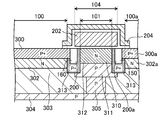
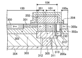
- each pixel includes a light receiving unit 100 that generates charges by photoelectric conversion, a charge holding unit 101 that accumulates charges generated by the light receiving unit 100, and charge holding of charges generated by the light receiving unit 100.
- a first charge transfer transistor 104 that controls transfer to the unit 101 and a second charge transfer transistor 105 that controls transfer of charges accumulated in the charge holding unit 101 are provided.
- Each pixel has a global reset transistor 103 having one end (drain) connected to the first power supply VDD1 and the other end (source) connected to the light receiving unit 100 and the first charge transfer transistor 104, and a gate electrode.
- a reset transistor 106 connected to the charge transfer transistor 105 and an output row select transistor 108 connected to the source of the source follower transistor 107 are provided.
- a third power supply VDD 3 is connected to the drain of the source follower transistor 107.
- a plurality of pixels are arranged in a matrix.
- the gate electrodes of the plurality of global reset transistors 103 provided in the pixels in the same row may be connected to the signal line 113 in common.
- the operation of the first charge transfer transistor 104 is controlled by the signal line 114 corresponding thereto.
- the operation of the second charge transfer transistor 105 is controlled by the signal line 115 corresponding thereto.
- the operation of the reset transistor 106 is controlled by the signal line 116 corresponding thereto.
- the operation of the output row select transistor 108 is controlled by the signal line 118 corresponding thereto.
- the light receiving unit 100 includes, for example, a p-type layer (first and second surface p-type layers 300 and 301) and an n-type layer 310 and stores electrons in the n-type layer 310.
- the structure is not limited as long as it has a function of storing electrons or holes generated by photoelectric conversion.
- the charge holding unit 101 only needs to have a configuration capable of holding a charge, and may be configured by, for example, an n-type layer 310 (floating diffusion layer) containing an n-type impurity of about 1 ⁇ 10 20 / cm 3. .
- the conductivity type of the global reset transistor 103, the reset transistor 106, the first charge transfer transistor 104, and the second charge transfer transistor 105 may be an n-channel type or a p-channel type.
- the voltage of the first power supply VDD1 is about 3.3 V, for example.
- the global reset transistor 103 becomes conductive and the light receiving unit 100 is reset. Is done.
- the voltage of the first power supply VDD1 only needs to be higher than the electrostatic potential when the light receiving unit 100 is depleted.
- a low voltage is applied to the gate electrode of the global reset transistor 103 to control the electrostatic potential between the first power supply VDD1 and the signal charge generated excessively in the light receiving unit 100 to the first power supply.
- An anti-blooming function may be provided that sweeps out to VDD1 and prevents signal charges from overflowing from the light receiving unit 100 to the charge holding unit 101.
- the global reset transistor 103 it is not always necessary to provide the global reset transistor 103 with an anti-blooming function, and the p-type impurity is set so that the electrostatic potential between the light receiving unit 100 and the n-type semiconductor substrate becomes 0V.
- an anti-blooming function by a vertical overflow drain can be provided.
- an electrostatic potential of about ⁇ 0.3 V is formed between the light receiving unit 100 and the charge holding unit 101 while the first charge transfer transistor 104 is off to prevent the transfer of electrons. But you can.
- a high voltage is applied to the gate electrode 202 of the first charge transfer transistor 104, and the electrostatic potential between the light receiving unit 100 and the charge holding unit 101 is changed. It should be higher than the maximum electrostatic potential at the time of depletion.
- the signal line Pixout provided for each column extends in the vertical direction, and the signal line 115 extends in the horizontal direction.
- the signal lines 113 and 114 may be arranged in parallel to the signal line Pixout.
- the direction in which the other signal lines and power supply lines extend can be changed as appropriate according to the layout.
- the power supply lines 121, 122, 123 corresponding to the power supply VDD2 and the third power supply VDD3 may be shared by a plurality of pixels.
- the output row select transistor 108 is not necessary when the power supply wirings 121, 122, and 123 are independent from each other.
- the charge holding unit via the second charge transfer transistor 105 in the selected row A signal is transferred from 101 to the charge-voltage converter 102.
- the output of the source follower transistor 107 in the corresponding row is read out to the signal line Pixout by the output row select transistor 108 in the selected row.
- the process from resetting the charge-voltage converter 102 to reading out the output signal is performed to read out the outputs of all the two-dimensionally arranged pixels.
- a global reset operation is performed by the global reset transistor 103 has been described.
- the global reset transistor 103 Even if the global reset transistor 103 is not provided, a vertical overflow drain is formed, and the first charges of all pixels before photoelectric conversion are performed.
- the gate electrode 202 of the transfer transistor 104 By setting the gate electrode 202 of the transfer transistor 104 to a high voltage, the charge of the light receiving unit 100 can be swept out. In this case, the above-described operation may be performed after the exposure time.
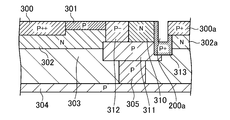
- a p-type layer 304 provided on an n-type substrate region (not shown) and electrically separating the substrate region and the light receiving unit 100, and a p-type layer An n-type layer 303 and a p-type layer 305 over the layer 304 are provided.
- the light receiving unit 100 provided on the semiconductor substrate includes an n-type layer 303, an n-type layer 302 provided on the n-type layer 303, a first surface p-type layer 300 provided on the n-type layer 302, and The second surface p-type layer 301 is constituted.
- the planar shape of the light receiving unit 100 is not particularly limited, but FIG. 3 shows an example of a quadrilateral shape.
- the charge holding unit 101 (that is, the n-type layer 310) is a p-type provided between the p-type layer (first p-type impurity region) 311 provided under the n-type layer 310 and the light receiving unit 100.
- the light receiving unit 100 is electrically separated by the layer.
- the p-type impurity concentration of the first surface p-type layer 300 is about 1 ⁇ 10 18 to 10 20 / cm 3
- the second surface p having a lower impurity concentration than the first surface p-type layer 300 is used.
- the p-type impurity concentration of the mold layer 301 is about 1 ⁇ 10 16 to 10 18 / cm 3 .
- the n-type impurity concentration of the n-type layer 302 is about 1 ⁇ 10 16 to 1 ⁇ 10 18 / cm 3
- the n-type impurity concentration of the n-type layer 303 is 1 ⁇ 10 14 to 1 ⁇ 10 17 / cm 3.
- the p-type impurity concentration of the p-type layer 304 is about 1 ⁇ 10 16 to 1 ⁇ 10 18 / cm 3
- the p-type impurity concentration of the p-type layer 305 is about 1 ⁇ 10 16 to 1 ⁇ 10 18 / cm 3
- the n-type impurity concentration of the n-type layer 310 is about 1 ⁇ 10 16 to 1 ⁇ 10 18 / cm 3 .
- the p-type impurity concentration of the p-type layer 311 is about 1 ⁇ 10 16 to 1 ⁇ 10 18 / cm 3 .
- the impurity concentration of the p-type layer (second p-type impurity region) 312 is lower than the impurity concentration of the p-type layers 301 and 311 and is about 1 ⁇ 10 16 to 1 ⁇ 10 18 / cm 3 .
- the first trench 200 formed in a region between the light receiving unit 100 and the charge holding unit 101 (n-type layer 310) in the semiconductor substrate and the semiconductor substrate out of each other.
- a second trench 200a formed in a region between the light receiving portions 100 and 100a of adjacent pixels is provided.
- the first insulating film 160 is provided.
- a metal layer or the like may be provided in the second insulating film 150.
- the depth of the first trench 200 and the second trench 200a may be about 50 to 300 nm, for example, and the width may be about 100 to 300 nm.
- the depths of the first trench 200 and the second trench 200a may be substantially the same as the depth of the n-type layer 310.
- a third trench 200b that surrounds the outer periphery of the light receiving units 100 and 100a and the charge holding unit 101, and a third insulating film 170 formed in the third trench 200b may be formed.
- an insulating film having a refractive index lower than that of the semiconductor substrate in the third trench 200b oblique light is reflected at the interface between the semiconductor substrate and the insulating film, and light incident on the light receiving unit 100 can be increased. it can.
- oblique light incident on the charge holding unit 101 can be further reduced.
- a transfer unit 201 that is provided in contact with the first insulating film 160 and serves as a charge transfer path from the light receiving unit 100 to the charge holding unit 101 is provided at the end of the boundary between the light receiving unit 100 and the charge holding unit 101. It has been.
- the transfer unit 201 is provided at a corner portion facing the charge holding unit 101. Since the transfer unit 201 is a region where the first trench 200 is not formed, the light shielding property of the charge holding unit 101 against oblique light is inferior to the region where the first trench 200 is provided.
- the amount of photoelectric conversion occurring in the transfer unit 201 can be suppressed, the parasitic signal can be reduced, and the image quality can be reduced. The influence can be suppressed. Further, by reducing the transfer unit 201 that cannot reflect the incident light by the first insulating film 160 from the center of the light receiving unit 100, it is possible to suppress a decrease in the incident light amount.
- the transfer unit 201 may be provided on the side opposite to the side in contact with the charge-voltage conversion unit 102 (position away from the charge-voltage conversion unit 102) when viewed from the center of the charge holding unit 101.
- the width of the portion of the n-type layer 310 adjacent to the transfer unit 201 is narrower than the width of the portion of the n-type layer 310 adjacent to the first trench 200, and the electrostatic potential at the time of depletion is reduced. Even when the voltage becomes low, charge transfer is unlikely to be hindered by being connected to the second charge transfer transistor 105 through a high electrostatic potential portion and a high electrostatic potential portion.
- the gate electrode 202 of the first charge transfer transistor 104 is provided on the charge holding portion 101 with a gate insulating film interposed therebetween.
- a light shielding film 204 is provided on the gate electrode 202 to cover the transfer portion and the gate electrode 202.
- the light shielding film 204 may be made of a metal such as tungsten.
- a gate electrode 203 of the second charge transfer transistor 105 is provided on a region between the charge holding unit 101 and the charge-voltage conversion unit 102 with a gate insulating film interposed therebetween.
- the planar shape of the light shielding film 204 is a quadrilateral, but is not limited to this shape.
- the light shielding film 204 only needs to cover at least the entire upper part of the charge holding unit 101 and the entire upper part of the transfer unit 201.
- the light shielding film 204 can prevent photoelectric conversion from being performed in the charge holding unit 101.
- the transfer unit 201 is moved from the end of the light shielding film 204 in the direction from the light receiving unit 100 to the charge holding unit 101 (the direction from left to right in FIG. 3) in plan view.
- the distance from the end of the light shielding film 204 to the charge holding unit 101 is longer than the distance from the end of the light shielding film 204 to the charge holding unit 101 through the first trench 200.
- the charge holding unit 100 and the charge holding unit are held by an electrostatic potential lower than ⁇ 0.3V, for example.
- the part 101 can be electrically separated.
- the width of the p-type layer 312 in the transfer unit 201 is preferably about 200 nm to 400 nm.
- the concentration of the n-type impurity contained in the portion in contact with the transfer unit 201 may be higher than the concentration of the n-type impurity contained in the other portion of the charge holding unit 101. Good.
- the corner portion of the charge holding unit 101 in contact with the transfer unit 201 has a recessed shape, if the n-type impurity concentration is uniform in the charge holding unit 101, Of these, the portion in contact with the transfer unit 201 has a narrow width, and therefore the amount of charge that can be accumulated is small.
- the electrostatic potential at the time of depletion is made lower than that of the n-type layer 310 adjacent to the first trench 200 by increasing the concentration of the n-type impurity contained in the portion of the charge holding unit 101 in contact with the transfer unit 201.
- the amount of charge that can be held in the charge holding unit 101 can be increased as long as the condition is maintained.
- a p-type layer 313 may be provided so as to surround the first trench 200 and the second trench 200a.
- the p-type layer 313 contains a p-type impurity of, for example, about 1 ⁇ 10 18 to 1 ⁇ 10 19 / cm 3 .
- the p-type impurity concentration included in the p-type layer 312 may be lower than the p-type impurity concentration included in the p-type layers 301 and 311.
- a depletion region formed by the p-type layer 312 and the n-type layer 302 is extended toward the charge holding unit 101, and charges generated by oblique light incident on the p-type layer 312 are moved to the light receiving unit 100.
- the movement of charges to the charge holding unit 101 can be prevented, and electronic crosstalk due to charge movement can be suppressed.
- the p-type impurity concentration of the p-type layer 312 is low, the charge transfer from the light receiving unit 100 to the charge holding unit 101 by the first charge transfer transistor 104 can be facilitated.
- the gate electrode 202 of the first charge transfer transistor 104 covers the upper portion of the charge holding unit 101, but the gate electrode 202 is formed between the light receiving unit 100 and the charge holding unit 101 in the semiconductor substrate. It may be provided above the p-type layer 312. In that case, a gate electrode to which another applied voltage is applied may be disposed above the charge holding portion 101, or the gate electrode may not be provided.
- a p-type layer containing a p-type impurity of about 1 ⁇ 10 16 to 1 ⁇ 10 18 / cm 3 is provided between the n-type layer 310 of the charge holding portion 101 and the gate insulating film below the gate electrode 202. It may be. Thereby, the dark current generated from the gate insulating film can be suppressed.
- FIG. 6A and FIG. 6B are cross-sectional views showing a method for manufacturing the solid-state imaging device of the present embodiment.
- a semiconductor substrate such as silicon containing n-type impurities is prepared.
- a p-type layer 304, a p-type layer 305, and a p-type layer 311 are formed in the semiconductor substrate using a known ion implantation method.
- a portion on the p-type layer 304 where the p-type layer 305 is not provided becomes an n-type layer 303.
- the first surface p-type layer 300, the second surface p-type layer 302, the p-type layers 312, 300a, 313, and the n-type Layers 302, 310, and 302a are formed, respectively. Thereby, the light receiving unit 100 and the charge holding unit 101 are formed.
- the first insulating film 160 is formed in the first trench 200, and the second trench 200a is formed in the second trench 200a.
- the insulating film 150 is embedded in the third trench 200b.
- the first trench 200, the second trench 200a, and the third trench 200b may be formed before the p-type layer and the n-type layer are formed.
- gate electrodes 202 and 203 made of polysilicon or the like are formed on the gate insulating film by a known method.
- a light shielding film 204 made of a metal such as tungsten covering the transfer portion 201 and the charge holding portion 101 is formed on the gate electrode 202 by a known method such as sputtering.
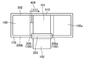
- FIG. 7 is a plan view showing a solid-state imaging device according to a first modification of the present embodiment.
- the gate electrode 202 is not shown.
- the part of the light receiving unit 100 that contacts the transfer unit 201 may protrude from the other part facing the charge holding unit 101.
- the light receiving unit 100 is extended to a region where the first trench 200 is not provided, it is possible to easily make light entering from the end of the light shielding film 204 enter the light receiving unit 100. For this reason, as will be described later, parasitic signals can be reduced. In addition, afterimage generation can be effectively suppressed.
- FIG. 8 is a plan view showing a solid-state imaging device according to a second modification of the present embodiment. As shown in the drawing, a portion of the light shielding film 204 provided above the transfer unit 201 may protrude toward the light receiving unit 100 as compared to a portion provided above the first trench 200. .
- FIG. 9 is a plan view showing a solid-state imaging device used for effect measurement.
- FIG. 10A, FIG. 10B, and FIG. 10C are diagrams showing the relationship between the buried trench ratio, the parasitic signal, the afterimage, and the dark current in the accumulation region, respectively.
- the buried trench ratio is assumed to be a value obtained by (length of the first trench 200) / (length of the light receiving unit 100 in the direction in which the first trench 200 extends).
- the inventors of the present application produced a plurality of solid-state imaging devices in which the length of the first trench 200 was changed, and measured parasitic signals and afterimages.
- the parasitic signal was measured by the following method. First, a high voltage is applied to the gate electrode of the global reset transistor 103, light is irradiated to the light receiving unit 100 without accumulating charges generated by photoelectric conversion, and the first charge transfer transistor 104 is turned off. Then, the charge accumulated in the charge holding portion 101 is output to the signal line 116 by the second charge transfer transistor 105. A parasitic signal photoelectrically converted by the charge holding unit 101 was measured by subtracting a signal that was operated in the same manner without irradiating light from the output signal.
- the afterimage was measured by the following method. First, the light that was photoelectrically converted by the light receiving unit 100 was irradiated so that a certain amount of charge was accumulated, and the signal was read to the signal line by a normal procedure. Next, in a state where light was not irradiated, the signal was read again to the signal line by a normal procedure, and the signal amount detected at this time was used as an afterimage.
- the optimum value of the buried trench ratio is considered to be about 50%.
- FIG. 11 is a plan view showing a solid-state imaging device used for effect measurement.
- FIG. 12 is a diagram illustrating the relationship between the position of the charge holding unit 101 and the magnitude of the parasitic signal.
- FIG. 12 shows the measurement results of the parasitic signals when the end position 403 of the charge holding unit 101 is changed to the positions 1 to 5 shown in FIG.
- FIG. 13 is a plan view showing a solid-state imaging device used for effect measurement.
- 14A is a diagram showing the relationship between the protruding portion position 404 of the light receiving unit (charge converting unit in the drawing) 100 and the parasitic signal
- FIG. 14B shows the relationship between the protruding portion position 404 of the light receiving unit 100 and the afterimage. It is a figure which shows a relationship.
- the protruding portion of the light receiving unit 100 specifically means a protruding portion of the n-type layer 302 to the transfer unit 201.
- FIG. 15A is a diagram illustrating a change in a parasitic signal when the p-type impurity concentration of the p-type layer 312 of the transfer unit 201 is changed in the solid-state image sensor
- FIG. 15B is a diagram illustrating the transfer unit 201 in the solid-state image sensor. It is a figure which shows the change of the afterimage when the p-type impurity density
- the parasitic signal gradually increased as the impurity concentration of the p-type layer 312 increased.
- an afterimage was generated when the impurity concentration of the p-type layer 312 became a predetermined value or more. From the above results, it can be said that the p-type impurity concentration of the p-type layer 312 is preferably low.
- the light incident on the charge holding unit 101 is blocked by the light shielding film 204, the first insulating film 160, and the second insulating film 150. Since charge transfer from the light receiving unit 100 to the charge holding unit 101 is possible, excellent image quality can be realized while taking advantage of the global shutter method.
- the solid-state imaging device disclosed in this specification is used in various imaging devices such as a camera.
- Second insulating film 100, 100a Light receiving unit 101 Charge holding unit 102 Charge voltage converting unit 103 Global reset transistor 104 First charge transfer transistor 105 Second charge transfer transistor 106 Reset transistor 107 Source follower transistor 108 Output row select transistor 113, 114, 116, 118 Signal lines 121, 122, 123 Power supply wiring 150 Second insulating film 160 First insulating film 170 Third insulating film 200 First trench 200a Second trench 200b Third trench 201 Transfer unit 202, 203 Gate Electrode 204 Light shielding film 300 First surface p-type layer 300a, 304, 305, 312, 313 p-type layer 301 Second surface p-type layer 302, 310, 302a, 303, 31 n-type layer
Abstract
This solid-state image pickup element is provided with pixels, each of which is provided with: a light receiving section (100); a charge holding section (101); a gate electrode (202); a first trench (200) formed in a region between the light receiving section and the charge holding section; a first insulating film (160) that is provided in the first trench; a transfer section (201); and a light blocking film (204) covering the charge holding section, transfer section, and gate electrode. In plan view, in the direction toward the charge holding section from the light receiving section, the distance from a light blocking film end to the charge holding section with the transfer section therebetween, is longer than the distance from the light blocking film end to the charge holding section with the first trench therebetween.
Description
本明細書に記載された技術は、固体撮像素子に関するものである。
The technology described in this specification relates to a solid-state imaging device.
画素が2次元状に配置されたMOS型固体撮像素子において、ローリングシャッター方式を用いた場合、高速に動く被写体を撮影する際に画像歪が発生してしまう。そこで、画像歪を無くすために、画素の撮像開始時と終了時を全画素で同時に行うグローバルシャッター方式を用いることが提案されている。
In a MOS type solid-state imaging device in which pixels are two-dimensionally arranged, when the rolling shutter method is used, image distortion occurs when shooting a subject that moves at high speed. Therefore, in order to eliminate image distortion, it has been proposed to use a global shutter system in which the start and end of pixel imaging are simultaneously performed for all pixels.
グローバルシャッター動作のためには、画素内に光電変換を行う光電変換部とは別に、撮像終了時から電荷読み出し時までの間、一時的に電荷を保持しておく電荷保持部が必要となる。光電変換部と電荷保持部のレイアウトとの関係は、例えば特許文献1に提案されている。
For the global shutter operation, apart from the photoelectric conversion unit that performs photoelectric conversion in the pixel, a charge holding unit that temporarily holds charge from the end of imaging to the time of charge reading is required. The relationship between the layout of the photoelectric conversion unit and the charge holding unit is proposed in Patent Document 1, for example.
電荷保持部を備えたグローバルシャッター方式の固体撮像素子においては、電荷保持部に電荷が保持される期間に画素領域に光が入射した場合でも、電荷保持部において光電変換が行われないことが求められる。そこで、例えば、上方からの入射光を遮るために、特許文献1に例示されているような、金属からなる遮光膜が電荷保持部の上方に設けられる。
In a global shutter type solid-state imaging device including a charge holding unit, it is required that photoelectric conversion is not performed in the charge holding unit even when light is incident on the pixel region during a period in which the charge is held in the charge holding unit. It is done. Therefore, for example, in order to block incident light from above, a light shielding film made of metal as exemplified in Patent Document 1 is provided above the charge holding portion.
しかし、電荷保持部の上方に設けられた遮光膜では、斜めに電荷保持部に入射する光を遮ることは難しい。半導体基板内部では光は直進してしまうため、遮光膜によって斜め入射光を遮るためには、電荷保持部の深さに応じて、電荷保持部の上方から光電変換部の上方に向かう方向に遮光膜を広げ、光電変換部の一部まで遮光膜で覆わなくてはならない。さらに、遮光膜端では光が回折するために、半導体基板に垂直に入射された光でも半導体基板中では斜めに進む光成分を持ってしまう。この斜めに進む光が電荷保持部に入射されてしまうことによる寄生信号は、光学的クロストークと呼ばれている。光学的クロストークの抑制はグローバルシャッター素子の画質改善のためには必須である。特許文献2には、トレンチ内に埋め込まれた絶縁膜を設け、半導体基板と絶縁膜との間の屈折率差によって半導体基板内部で入射光を反射させることが提案されている。
However, it is difficult to block light incident on the charge holding portion obliquely with the light shielding film provided above the charge holding portion. Since light travels straight inside the semiconductor substrate, in order to block obliquely incident light by the light-shielding film, light is shielded in a direction from above the charge holding unit to above the photoelectric conversion unit according to the depth of the charge holding unit. The film must be expanded and part of the photoelectric conversion part must be covered with a light-shielding film. Further, since the light is diffracted at the end of the light shielding film, even the light incident perpendicularly to the semiconductor substrate has a light component traveling obliquely in the semiconductor substrate. This parasitic signal caused by the obliquely incident light entering the charge holding portion is called optical crosstalk. Suppression of optical crosstalk is essential for improving the image quality of the global shutter element. Patent Document 2 proposes that an insulating film embedded in a trench is provided and incident light is reflected inside the semiconductor substrate due to a difference in refractive index between the semiconductor substrate and the insulating film.
特許文献1及び特許文献2に記載の技術では、いずれも光学的クロストークを効果的に低減することは難しい。
In the techniques described in Patent Document 1 and Patent Document 2, it is difficult to effectively reduce optical crosstalk.
本明細書に開示された技術は、光学的クロストークを大幅に低減できる固体撮像素子を提供することを目的とする。
The technique disclosed in this specification is intended to provide a solid-state imaging device capable of greatly reducing optical crosstalk.
本明細書に開示された固体撮像素子は、複数の画素が配置された撮像領域を備えている。前記画素の各々には、半導体基板に設けられ、光電変換により電荷を発生させる受光部と、前記半導体基板に設けられ、前記受光部で生じた電荷を蓄積する電荷保持部と、前記電荷保持部上に設けられ、前記受光部で生じた電荷を前記電荷保持部へと転送させるゲート電極と、前記半導体基板のうち、前記受光部と前記電荷保持部との間の領域に形成された第1のトレンチと、前記第1のトレンチ内に設けられた第1の絶縁膜と、前記半導体基板のうち、互いに隣接する画素の受光部の間の領域に形成された第2のトレンチと、前記第2のトレンチ内に設けられた第2の絶縁膜と、前記受光部と前記電荷保持部との境界の端部に前記第1の絶縁膜に接して設けられ、前記受光部から前記電荷保持部への電荷の転送経路となる転送部と、前記電荷保持部、前記転送部及び前記ゲート電極上を覆う遮光膜とが設けられている。平面視において、前記受光部から前記電荷保持部へと向かう方向の、前記遮光膜の端から前記転送部を挟んで前記電荷保持部に至るまでの距離は、前記遮光膜の端から前記第1のトレンチを挟んで前記電荷保持部に至るまでの距離よりも長い。
The solid-state imaging device disclosed in this specification includes an imaging region in which a plurality of pixels are arranged. In each of the pixels, a light receiving portion provided on a semiconductor substrate and generating charges by photoelectric conversion, a charge holding portion provided on the semiconductor substrate and storing charges generated in the light receiving portion, and the charge holding portion A gate electrode provided on the light-receiving portion for transferring the charge generated in the light-receiving portion to the charge holding portion; and a first electrode formed in a region of the semiconductor substrate between the light-receiving portion and the charge holding portion. A first insulating film provided in the first trench, a second trench formed in a region between light receiving portions of adjacent pixels of the semiconductor substrate, and the first trench A second insulating film provided in the trench of 2 and an end of a boundary between the light receiving unit and the charge holding unit provided in contact with the first insulating film, from the light receiving unit to the charge holding unit A transfer section serving as a charge transfer path to the Holding portion, and a light shielding film is provided to cover the transfer unit and the gate electrode electrode. In a plan view, the distance from the end of the light shielding film to the charge holding unit across the transfer unit in the direction from the light receiving unit to the charge holding unit is the first distance from the end of the light shielding film to the first holding unit. Longer than the distance to the charge holding portion across the trench.
本明細書に開示された固体撮像素子によれば、光学的クロストークを大幅に低減しうる。
According to the solid-state imaging device disclosed in this specification, optical crosstalk can be significantly reduced.
以下、本発明の実施形態を図面に基づいて詳細に説明する。
Hereinafter, embodiments of the present invention will be described in detail with reference to the drawings.
(実施形態)
図1は、本開示の実施形態に係る固体撮像素子の画素回路の構成を示す回路図である。図2は、本実施形態の固体撮像素子を模式的に示す平面図である。図3は、本実施形態の固体撮像素子における画素の構成を示す平面図であり、図4は、図3に示す固体撮像素子のIV-IV線での断面を示す断面図であり、図5は、図3に示す固体撮像素子のV-V線での断面を示す断面図である。図3では、構成が理解しやすいように、遮光膜204の下に設けられた部材も示している。 (Embodiment)
FIG. 1 is a circuit diagram illustrating a configuration of a pixel circuit of a solid-state imaging device according to an embodiment of the present disclosure. FIG. 2 is a plan view schematically showing the solid-state imaging device of the present embodiment. FIG. 3 is a plan view showing a configuration of a pixel in the solid-state imaging device of the present embodiment, and FIG. 4 is a cross-sectional view showing a cross section taken along line IV-IV of the solid-state imaging device shown in FIG. FIG. 5 is a cross-sectional view showing a cross section taken along line VV of the solid-state imaging device shown in FIG. In FIG. 3, members provided under thelight shielding film 204 are also shown for easy understanding of the configuration.
図1は、本開示の実施形態に係る固体撮像素子の画素回路の構成を示す回路図である。図2は、本実施形態の固体撮像素子を模式的に示す平面図である。図3は、本実施形態の固体撮像素子における画素の構成を示す平面図であり、図4は、図3に示す固体撮像素子のIV-IV線での断面を示す断面図であり、図5は、図3に示す固体撮像素子のV-V線での断面を示す断面図である。図3では、構成が理解しやすいように、遮光膜204の下に設けられた部材も示している。 (Embodiment)
FIG. 1 is a circuit diagram illustrating a configuration of a pixel circuit of a solid-state imaging device according to an embodiment of the present disclosure. FIG. 2 is a plan view schematically showing the solid-state imaging device of the present embodiment. FIG. 3 is a plan view showing a configuration of a pixel in the solid-state imaging device of the present embodiment, and FIG. 4 is a cross-sectional view showing a cross section taken along line IV-IV of the solid-state imaging device shown in FIG. FIG. 5 is a cross-sectional view showing a cross section taken along line VV of the solid-state imaging device shown in FIG. In FIG. 3, members provided under the
本実施形態の固体撮像素子は、複数の画素が例えば行列状に配置された撮像領域(図示せず)を備えている。各画素には、図1に示すように、光電変換により電荷を発生させる受光部100と、受光部100で生じた電荷を蓄積する電荷保持部101と、受光部100で生じた電荷の電荷保持部101への転送を制御する第1の電荷転送トランジスタ104と、電荷保持部101に蓄積された電荷の転送を制御する第2の電荷転送トランジスタ105とが設けられている。また、各画素には、一端(ドレイン)が第1の電源VDD1に接続され、他端(ソース)が受光部100及び第1の電荷転送トランジスタ104に接続されたグローバルリセットトランジスタ103と、ゲート電極が電荷電圧変換部102を挟んで第2の電荷転送トランジスタ105に接続されたソースフォロワートランジスタ107と、一端が第2の電源VDD2に接続され、他端が電荷電圧変換部102を挟んで第2の電荷転送トランジスタ105に接続されたリセットトランジスタ106と、ソースフォロワートランジスタ107のソースに接続された出力行セレクトトランジスタ108とが設けられている。ソースフォロワートランジスタ107のドレインには、第3の電源VDD3が接続されている。
The solid-state imaging device of the present embodiment includes an imaging region (not shown) in which a plurality of pixels are arranged in a matrix, for example. As shown in FIG. 1, each pixel includes a light receiving unit 100 that generates charges by photoelectric conversion, a charge holding unit 101 that accumulates charges generated by the light receiving unit 100, and charge holding of charges generated by the light receiving unit 100. A first charge transfer transistor 104 that controls transfer to the unit 101 and a second charge transfer transistor 105 that controls transfer of charges accumulated in the charge holding unit 101 are provided. Each pixel has a global reset transistor 103 having one end (drain) connected to the first power supply VDD1 and the other end (source) connected to the light receiving unit 100 and the first charge transfer transistor 104, and a gate electrode. Has a source follower transistor 107 connected to the second charge transfer transistor 105 across the charge voltage converter 102, one end connected to the second power supply VDD2, and the other end connected to the second voltage transfer unit 102 across the charge voltage converter 102. A reset transistor 106 connected to the charge transfer transistor 105 and an output row select transistor 108 connected to the source of the source follower transistor 107 are provided. A third power supply VDD 3 is connected to the drain of the source follower transistor 107.
図2に示すように、複数の画素は行列状に配置されている。同一行の画素内に設けられた複数のグローバルリセットトランジスタ103のゲート電極は、信号線113に共通に接続されていてもよい。第1の電荷転送トランジスタ104の動作は、これに対応する信号線114によって制御される。第2の電荷転送トランジスタ105の動作は、これに対応する信号線115によって制御される。リセットトランジスタ106の動作は、これに対応する信号線116によって制御される。出力行セレクトトランジスタ108の動作は、これに対応する信号線118によって制御される。
As shown in FIG. 2, a plurality of pixels are arranged in a matrix. The gate electrodes of the plurality of global reset transistors 103 provided in the pixels in the same row may be connected to the signal line 113 in common. The operation of the first charge transfer transistor 104 is controlled by the signal line 114 corresponding thereto. The operation of the second charge transfer transistor 105 is controlled by the signal line 115 corresponding thereto. The operation of the reset transistor 106 is controlled by the signal line 116 corresponding thereto. The operation of the output row select transistor 108 is controlled by the signal line 118 corresponding thereto.
図3に示すように、受光部100は、例えばp型層(第1及び第2の表面p型層300、301)とn型層310とで構成され、n型層310に電子を蓄える埋め込み型フォトダイオードであってもよいが、光電変換により生じた電子又はホールを蓄える機能を有していれば、その構成は限定されない。電荷保持部101は、電荷を保持できる構成を有していればよく、例えば1×10²⁰/cm3程度のn型不純物を含むn型層310(フローティング拡散層)により構成されていてもよい。
As shown in FIG. 3, the light receiving unit 100 includes, for example, a p-type layer (first and second surface p-type layers 300 and 301) and an n-type layer 310 and stores electrons in the n-type layer 310. However, the structure is not limited as long as it has a function of storing electrons or holes generated by photoelectric conversion. The charge holding unit 101 only needs to have a configuration capable of holding a charge, and may be configured by, for example, an n-type layer 310 (floating diffusion layer) containing an n-type impurity of about 1 × 10 20 / cm 3. .
グローバルリセットトランジスタ103、リセットトランジスタ106、第1の電荷転送トランジスタ104及び第2の電荷転送トランジスタ105の導電型はnチャネル型であってもよいし、pチャネル型であってもよい。
The conductivity type of the global reset transistor 103, the reset transistor 106, the first charge transfer transistor 104, and the second charge transfer transistor 105 may be an n-channel type or a p-channel type.
グローバルリセットトランジスタ103がnチャネル型の場合、第1の電源VDD1の電圧が例えば3.3V程度であり、ゲート電極に高電圧が印加されるとグローバルリセットトランジスタ103が導通し、受光部100がリセットされる。第1の電源VDD1の電圧は、受光部100の空乏化時の静電ポテンシャルよりも高ければよい。
When the global reset transistor 103 is an n-channel type, the voltage of the first power supply VDD1 is about 3.3 V, for example. When a high voltage is applied to the gate electrode, the global reset transistor 103 becomes conductive and the light receiving unit 100 is reset. Is done. The voltage of the first power supply VDD1 only needs to be higher than the electrostatic potential when the light receiving unit 100 is depleted.
光電変換時にはグローバルリセットトランジスタ103のゲート電極に低い電圧を印加し、第1の電源VDD1との間の静電ポテンシャルを制御することで、受光部100において過剰に発生した信号電荷を第1の電源VDD1へと掃出し、受光部100から電荷保持部101へ信号電荷があふれ出さないようにする、アンチブルーミング機能を持たせてもよい。ただし、n型半導体基板を用いる場合は、必ずしもグローバルリセットトランジスタ103にアンチブルーミング機能を持たせる必要は無く、受光部100とn型半導体基板間の静電ポテンシャルを0Vになるようにp型不純物の濃度を制御することで、縦型オーバーフロードレインによるアンチブルーミング機能を持たせることもできる。
At the time of photoelectric conversion, a low voltage is applied to the gate electrode of the global reset transistor 103 to control the electrostatic potential between the first power supply VDD1 and the signal charge generated excessively in the light receiving unit 100 to the first power supply. An anti-blooming function may be provided that sweeps out to VDD1 and prevents signal charges from overflowing from the light receiving unit 100 to the charge holding unit 101. However, when an n-type semiconductor substrate is used, it is not always necessary to provide the global reset transistor 103 with an anti-blooming function, and the p-type impurity is set so that the electrostatic potential between the light receiving unit 100 and the n-type semiconductor substrate becomes 0V. By controlling the concentration, an anti-blooming function by a vertical overflow drain can be provided.
信号電荷が電子である場合、第1の電荷転送トランジスタ104がオフの期間、受光部100と電荷保持部101との間に-0.3V程度の静電ポテンシャルを形成し、電子の転送を防いでもよい。受光部100から電荷を転送する際には、第1の電荷転送トランジスタ104のゲート電極202に高電圧を印加し、受光部100と電荷保持部101の間の静電ポテンシャルを、受光部100の空乏時の静電ポテンシャルの最大値よりも高くなるようにする。
When the signal charge is an electron, an electrostatic potential of about −0.3 V is formed between the light receiving unit 100 and the charge holding unit 101 while the first charge transfer transistor 104 is off to prevent the transfer of electrons. But you can. When transferring charges from the light receiving unit 100, a high voltage is applied to the gate electrode 202 of the first charge transfer transistor 104, and the electrostatic potential between the light receiving unit 100 and the charge holding unit 101 is changed. It should be higher than the maximum electrostatic potential at the time of depletion.
図2に示すように、列ごとに設けられた信号線Pixoutは縦方向に延びており、信号線115は横方向に延びている。信号線113、114は、信号線Pixoutに対して平行に配置されていてもよい。他の信号線や電源配線の延びる方向は、レイアウトに応じて適宜変更可能である。なお、電荷電圧変換部102、リセットトランジスタ106、ソースフォロワートランジスタ107、出力行セレクトトランジスタ108や、各トランジスタを制御するための信号線113、114、116、118、第1の電源VDD1、第2の電源VDD2、第3の電源VDD3にそれぞれ対応した電源配線121、122、123は、複数の画素で共有されてもよい。出力行セレクトトランジスタ108は、電源配線121、122、123が互いに独立した配線である場合には、不要である。
As shown in FIG. 2, the signal line Pixout provided for each column extends in the vertical direction, and the signal line 115 extends in the horizontal direction. The signal lines 113 and 114 may be arranged in parallel to the signal line Pixout. The direction in which the other signal lines and power supply lines extend can be changed as appropriate according to the layout. The charge-voltage converter 102, the reset transistor 106, the source follower transistor 107, the output row select transistor 108, the signal lines 113, 114, 116, and 118 for controlling each transistor, the first power supply VDD1, the second The power supply lines 121, 122, 123 corresponding to the power supply VDD2 and the third power supply VDD3 may be shared by a plurality of pixels. The output row select transistor 108 is not necessary when the power supply wirings 121, 122, and 123 are independent from each other.
次に、固体撮像素子の動作を説明する。まず、グローバルリセットトランジスタ103のゲート電極に高電圧を印加することにより、受光部100で生じた電荷を全て掃き出す。その後、光電変換を開始する。ある露光時間が過ぎた後、全画素内の第2の電荷転送トランジスタ105とリセットトランジスタ106を導通状態にして電荷保持部101の電荷を全て掃き出す。その後、第2の電荷転送トランジスタ105を非導通状態にして、第1の電荷転送トランジスタ104のゲート電極に高電圧を印加することで、受光部100から電荷保持部101へと信号電荷を転送する。ここで、グローバルリセットトランジスタ103による電荷の掃出しと、第1の電荷転送トランジスタ104による電荷の転送を全ての画素で同時に行うことで、画素の撮像開始時と終了時を全画素で同時に行うグローバルシャッター動作が実現される。
Next, the operation of the solid-state image sensor will be described. First, by applying a high voltage to the gate electrode of the global reset transistor 103, all charges generated in the light receiving unit 100 are swept out. Thereafter, photoelectric conversion is started. After a certain exposure time has passed, the second charge transfer transistor 105 and the reset transistor 106 in all the pixels are turned on to sweep out all charges in the charge holding unit 101. Thereafter, the second charge transfer transistor 105 is turned off and a high voltage is applied to the gate electrode of the first charge transfer transistor 104 to transfer the signal charge from the light receiving unit 100 to the charge holding unit 101. . Here, the global shutter that simultaneously performs the sweeping of charges by the global reset transistor 103 and the transfer of charges by the first charge transfer transistor 104 in all pixels simultaneously at the start and end of pixel imaging. Operation is realized.
次に、特定行のリセットトランジスタ106を介して電荷電圧変換部102の電圧を第2の電源の電圧にリセットした後に、選択された行の第2の電荷転送トランジスタ105を介して、電荷保持部101から電荷電圧変換部102へと信号を転送する。次いで、選択された行の出力行セレクトトランジスタ108により該当行のソースフォロワートランジスタ107の出力のみを信号線Pixoutへと読み出す。行を変えながら、上記の電荷電圧変換部102のリセットから出力信号の読み出しまでを行い、2次元配置されたすべての画素の出力を読み出す。ここでは、グローバルリセットトランジスタ103によりグローバルリセット動作を行う例を説明したが、グローバルリセットトランジスタ103が無くても、縦型オーバーフロードレインを形成し、光電変換を行う前にすべての画素の第1の電荷転送トランジスタ104のゲート電極202を高い電圧にすることで、受光部100の電荷を掃き出すことは可能である。この場合、露光時間後、上述した動作を行えばよい。
Next, after resetting the voltage of the charge-voltage conversion unit 102 to the voltage of the second power supply via the reset transistor 106 in the specific row, the charge holding unit via the second charge transfer transistor 105 in the selected row A signal is transferred from 101 to the charge-voltage converter 102. Next, only the output of the source follower transistor 107 in the corresponding row is read out to the signal line Pixout by the output row select transistor 108 in the selected row. While changing the row, the process from resetting the charge-voltage converter 102 to reading out the output signal is performed to read out the outputs of all the two-dimensionally arranged pixels. Here, an example in which a global reset operation is performed by the global reset transistor 103 has been described. However, even if the global reset transistor 103 is not provided, a vertical overflow drain is formed, and the first charges of all pixels before photoelectric conversion are performed. By setting the gate electrode 202 of the transfer transistor 104 to a high voltage, the charge of the light receiving unit 100 can be swept out. In this case, the above-described operation may be performed after the exposure time.
次に、本実施形態の固体撮像素子のより具体的な構成を説明する。
Next, a more specific configuration of the solid-state imaging device of the present embodiment will be described.
図3~図5に示すように、半導体基板において、n型の基板領域(図示せず)上に設けられ、基板領域と受光部100とを電気的に分離するp型層304と、p型層304上のn型層303及びp型層305が設けられている。
As shown in FIGS. 3 to 5, in a semiconductor substrate, a p-type layer 304 provided on an n-type substrate region (not shown) and electrically separating the substrate region and the light receiving unit 100, and a p-type layer An n-type layer 303 and a p-type layer 305 over the layer 304 are provided.
半導体基板に設けられた受光部100は、n型層303と、n型層303上に設けられたn型層302と、n型層302上に設けられた第1の表面p型層300及び第2の表面p型層301とにより構成されている。受光部100の平面形状は特に限定されないが、図3では、四辺形状である例を示している。
The light receiving unit 100 provided on the semiconductor substrate includes an n-type layer 303, an n-type layer 302 provided on the n-type layer 303, a first surface p-type layer 300 provided on the n-type layer 302, and The second surface p-type layer 301 is constituted. The planar shape of the light receiving unit 100 is not particularly limited, but FIG. 3 shows an example of a quadrilateral shape.
電荷保持部101(すなわちn型層310)は、n型層310の下に設けられたp型層(第1のp型不純物領域)311と、受光部100との間に設けられたp型層とによって、受光部100と電気的に分離されている。なお、第1の表面p型層300のp型不純物濃度は、1×10¹⁸~1020/cm3程度であり、第1の表面p型層300よりも不純物濃度の低い第2の表面p型層301のp型不純物濃度は、1×1016~1018/cm3程度である。n型層302のn型不純物濃度は、1×1016~1×1018/cm3程度であり、n型層303のn型不純物濃度は、1×1014~1×1017/cm3程度である。p型層304のp型不純物濃度は、1×1016~1×1018/cm3程度である。p型層305のp型不純物濃度は、1×1016~1×1018/cm3程度である。n型層310のn型不純物濃度は、1×1016~1×1018/cm3程度である。p型層311のp型不純物濃度は、1×1016~1×1018/cm3程度である。p型層(第2のp型不純物領域)312の不純物濃度はp型層301、311の不純物濃度よりも低く、1×1016~1×1018/cm3程度である。
The charge holding unit 101 (that is, the n-type layer 310) is a p-type provided between the p-type layer (first p-type impurity region) 311 provided under the n-type layer 310 and the light receiving unit 100. The light receiving unit 100 is electrically separated by the layer. The p-type impurity concentration of the first surface p-type layer 300 is about 1 × 10 18 to 10 20 / cm 3 , and the second surface p having a lower impurity concentration than the first surface p-type layer 300 is used. The p-type impurity concentration of the mold layer 301 is about 1 × 10 16 to 10 18 / cm 3 . The n-type impurity concentration of the n-type layer 302 is about 1 × 10 16 to 1 × 10 18 / cm 3 , and the n-type impurity concentration of the n-type layer 303 is 1 × 10 14 to 1 × 10 17 / cm 3. Degree. The p-type impurity concentration of the p-type layer 304 is about 1 × 10 16 to 1 × 10 18 / cm 3 . The p-type impurity concentration of the p-type layer 305 is about 1 × 10 16 to 1 × 10 18 / cm 3 . The n-type impurity concentration of the n-type layer 310 is about 1 × 10 16 to 1 × 10 18 / cm 3 . The p-type impurity concentration of the p-type layer 311 is about 1 × 10 16 to 1 × 10 18 / cm 3 . The impurity concentration of the p-type layer (second p-type impurity region) 312 is lower than the impurity concentration of the p- type layers 301 and 311 and is about 1 × 10 16 to 1 × 10 18 / cm 3 .
本実施形態の固体撮像素子では、半導体基板のうち、受光部100と電荷保持部101(n型層310)との間の領域に形成された第1のトレンチ200と、半導体基板のうち、互いに隣接する画素の受光部100、100aの間の領域に形成された第2のトレンチ200aとが設けられている。第1のトレンチ200内及び第2のトレンチ200a内には、シリコン酸化物等、半導体基板よりも屈折率の低い材料からなる第1の絶縁膜160、第2の絶縁膜150がそれぞれ埋め込まれている。ここで、受光部100と電荷保持部101との間の電気的分離、及び互いに隣接する受光部100と受光部100aとの間の電気的分離が確保されていれば、第1の絶縁膜160及び第2の絶縁膜150内に金属層等が設けられていてもよい。
In the solid-state imaging device of the present embodiment, the first trench 200 formed in a region between the light receiving unit 100 and the charge holding unit 101 (n-type layer 310) in the semiconductor substrate and the semiconductor substrate out of each other. A second trench 200a formed in a region between the light receiving portions 100 and 100a of adjacent pixels is provided. A first insulating film 160 and a second insulating film 150 made of a material having a refractive index lower than that of the semiconductor substrate, such as silicon oxide, are embedded in the first trench 200 and the second trench 200a, respectively. Yes. Here, if electrical isolation between the light receiving unit 100 and the charge holding unit 101 and electrical isolation between the light receiving unit 100 and the light receiving unit 100a adjacent to each other are ensured, the first insulating film 160 is provided. In addition, a metal layer or the like may be provided in the second insulating film 150.
第1のトレンチ200及び第2のトレンチ200aの深さは例えば50~300nm程度であり、幅は100~300nm程度であってもよい。第1のトレンチ200及び第2のトレンチ200aの深さは、n型層310の深さと同程度であってもよい。
The depth of the first trench 200 and the second trench 200a may be about 50 to 300 nm, for example, and the width may be about 100 to 300 nm. The depths of the first trench 200 and the second trench 200a may be substantially the same as the depth of the n-type layer 310.
受光部100、100aと電荷保持部101の外周を囲む第3のトレンチ200bと、第3のトレンチ200b内に形成された第3の絶縁膜170とが形成されていてもよい。第3のトレンチ200b内に半導体基板よりも屈折率の低い絶縁膜を形成することにより、半導体基板と当該絶縁膜との界面で斜め光を反射させ、受光部100に入射する光を増やすことができる。また、電荷保持部101に入射する斜め光をより低減することができる。
A third trench 200b that surrounds the outer periphery of the light receiving units 100 and 100a and the charge holding unit 101, and a third insulating film 170 formed in the third trench 200b may be formed. By forming an insulating film having a refractive index lower than that of the semiconductor substrate in the third trench 200b, oblique light is reflected at the interface between the semiconductor substrate and the insulating film, and light incident on the light receiving unit 100 can be increased. it can. In addition, oblique light incident on the charge holding unit 101 can be further reduced.
受光部100と電荷保持部101との境界の端部には、第1の絶縁膜160に接して設けられ、受光部100から電荷保持部101への電荷の転送経路となる転送部201が設けられている。受光部100の平面形状が四辺形の場合、転送部201は、電荷保持部101に面したコーナー部に設けられることになる。転送部201は第1のトレンチ200が形成されない領域であるので、斜め光に対する電荷保持部101の遮光性が、第1のトレンチ200が設けられる領域に比べて劣る。入射光強度は、受光部100の中心から離れるに従って落ちるので、転送部201を上記位置に配置することにより、転送部201において光電変換が発生する量を抑制し、寄生信号を小さくし、画質に対する影響を抑制することができる。また、第1の絶縁膜160により入射光を反射させることができない転送部201を受光部100の中心から離すことにより、入射光量の減少を抑えることもできる。
A transfer unit 201 that is provided in contact with the first insulating film 160 and serves as a charge transfer path from the light receiving unit 100 to the charge holding unit 101 is provided at the end of the boundary between the light receiving unit 100 and the charge holding unit 101. It has been. When the planar shape of the light receiving unit 100 is a quadrilateral, the transfer unit 201 is provided at a corner portion facing the charge holding unit 101. Since the transfer unit 201 is a region where the first trench 200 is not formed, the light shielding property of the charge holding unit 101 against oblique light is inferior to the region where the first trench 200 is provided. Since the incident light intensity decreases as the distance from the center of the light receiving unit 100 decreases, the amount of photoelectric conversion occurring in the transfer unit 201 can be suppressed, the parasitic signal can be reduced, and the image quality can be reduced. The influence can be suppressed. Further, by reducing the transfer unit 201 that cannot reflect the incident light by the first insulating film 160 from the center of the light receiving unit 100, it is possible to suppress a decrease in the incident light amount.
平面視において、転送部201は、電荷保持部101の中心から見て、電荷電圧変換部102に接する辺と反対側(電荷電圧変換部102から離れた位置)に設けられていてもよい。この構造により、n型層310のうち転送部201に隣接する部分の幅が、n型層310のうち第1のトレンチ200に隣接する部分の幅よりも狭くなり、空乏化時の静電ポテンシャルが低くなる場合でも、静電ポテンシャルが低い部分から高い部分を介して第2の電荷転送トランジスタ105へと接続されることにより、電荷転送が阻害されにくくなる。
In plan view, the transfer unit 201 may be provided on the side opposite to the side in contact with the charge-voltage conversion unit 102 (position away from the charge-voltage conversion unit 102) when viewed from the center of the charge holding unit 101. With this structure, the width of the portion of the n-type layer 310 adjacent to the transfer unit 201 is narrower than the width of the portion of the n-type layer 310 adjacent to the first trench 200, and the electrostatic potential at the time of depletion is reduced. Even when the voltage becomes low, charge transfer is unlikely to be hindered by being connected to the second charge transfer transistor 105 through a high electrostatic potential portion and a high electrostatic potential portion.
また、電荷保持部101上には、ゲート絶縁膜を挟んで第1の電荷転送トランジスタ104のゲート電極202が設けられる。ゲート電極202上には、転送部及びゲート電極202を覆う遮光膜204が設けられている。遮光膜204は、例えばタングステン等の金属により構成されていてもよい。また、電荷保持部101と電荷電圧変換部102との間の領域上には、ゲート絶縁膜を挟んで第2の電荷転送トランジスタ105のゲート電極203が設けられている。
Further, the gate electrode 202 of the first charge transfer transistor 104 is provided on the charge holding portion 101 with a gate insulating film interposed therebetween. A light shielding film 204 is provided on the gate electrode 202 to cover the transfer portion and the gate electrode 202. The light shielding film 204 may be made of a metal such as tungsten. Further, a gate electrode 203 of the second charge transfer transistor 105 is provided on a region between the charge holding unit 101 and the charge-voltage conversion unit 102 with a gate insulating film interposed therebetween.
図3に示す例では、遮光膜204の平面形状は四辺形であるが、この形に限定されない。遮光膜204は少なくとも電荷保持部101の上方全体と転送部201の上方全体を覆っていればよい。遮光膜204により、電荷保持部101で光電変換が行われるのを防ぐことができる。
In the example shown in FIG. 3, the planar shape of the light shielding film 204 is a quadrilateral, but is not limited to this shape. The light shielding film 204 only needs to cover at least the entire upper part of the charge holding unit 101 and the entire upper part of the transfer unit 201. The light shielding film 204 can prevent photoelectric conversion from being performed in the charge holding unit 101.
また、本実施形態の固体撮像素子では、平面視において、受光部100から電荷保持部101へと向かう方向(図3の左から右へ向かう方向)の、遮光膜204の端から転送部201を挟んで電荷保持部101に至るまでの距離は、遮光膜204の端から第1のトレンチ200を挟んで電荷保持部101に至るまでの距離よりも長くなっている。この構成により、遮光膜204の端部から回折によって回り込む光を電荷保持部101に入射させにくくすることができるので、光学的クロストークを生じにくくすることができる。n型層302と電荷保持部101との距離を大きくすることにより、p型層312のp型不純物濃度を低くしても例えば-0.3Vよりも低い静電ポテンシャルによって受光部100と電荷保持部101とを電気的に分離することが可能となる。転送部201におけるp型層312の幅は、200nm以上400nm以下程度であることが好ましい。電荷保持部101のうち、第1のトレンチ200に隣接する部分の幅をできるだけ大きくすることで、電荷保持部101に蓄積できる電荷量を大きくすることができる。
In the solid-state imaging device of the present embodiment, the transfer unit 201 is moved from the end of the light shielding film 204 in the direction from the light receiving unit 100 to the charge holding unit 101 (the direction from left to right in FIG. 3) in plan view. The distance from the end of the light shielding film 204 to the charge holding unit 101 is longer than the distance from the end of the light shielding film 204 to the charge holding unit 101 through the first trench 200. With this configuration, it is possible to make it difficult for light that diffracts from the end of the light shielding film 204 to enter the charge holding unit 101, so that optical crosstalk can be made difficult to occur. By increasing the distance between the n-type layer 302 and the charge holding unit 101, even if the p-type impurity concentration of the p-type layer 312 is decreased, the charge holding unit 100 and the charge holding unit are held by an electrostatic potential lower than −0.3V, for example. The part 101 can be electrically separated. The width of the p-type layer 312 in the transfer unit 201 is preferably about 200 nm to 400 nm. By increasing the width of the portion of the charge holding portion 101 adjacent to the first trench 200 as much as possible, the amount of charge that can be accumulated in the charge holding portion 101 can be increased.
なお、電荷保持部101の平面面積が小さくなると、蓄積できる電荷量が減ってしまうため、遮光膜204の端から第1のトレンチ200を挟んで電荷保持部101に至るまでの距離は、後述のように適切な値にすることが好ましい。
Note that when the planar area of the charge holding portion 101 is reduced, the amount of charge that can be accumulated is reduced. Therefore, the distance from the end of the light shielding film 204 to the charge holding portion 101 across the first trench 200 is described later. Thus, it is preferable to set an appropriate value.
電荷保持部101(n型層310)のうち、転送部201に接する部分に含まれるn型不純物の濃度は、電荷保持部101の他の部分に含まれるn型不純物の濃度よりも高くてもよい。図3に示す例では、転送部201と接する電荷保持部101のコーナー部が凹んだ形状となっているので、電荷保持部101内でn型不純物濃度が均一であると、電荷保持部101のうち転送部201に接する部分は、その幅が狭いため、蓄積できる電荷量が小さくなる。電荷保持部101のうち、転送部201に接する部分に含まれるn型不純物の濃度を高くすることにより、第1のトレンチ200に隣接するn型層310より空乏化時の静電ポテンシャルを低くする条件を保つ範囲で、電荷保持部101に保持可能な電荷量を増やすことができる。
Of the charge holding unit 101 (n-type layer 310), the concentration of the n-type impurity contained in the portion in contact with the transfer unit 201 may be higher than the concentration of the n-type impurity contained in the other portion of the charge holding unit 101. Good. In the example shown in FIG. 3, since the corner portion of the charge holding unit 101 in contact with the transfer unit 201 has a recessed shape, if the n-type impurity concentration is uniform in the charge holding unit 101, Of these, the portion in contact with the transfer unit 201 has a narrow width, and therefore the amount of charge that can be accumulated is small. The electrostatic potential at the time of depletion is made lower than that of the n-type layer 310 adjacent to the first trench 200 by increasing the concentration of the n-type impurity contained in the portion of the charge holding unit 101 in contact with the transfer unit 201. The amount of charge that can be held in the charge holding unit 101 can be increased as long as the condition is maintained.
また、図4、5に示すように、第1のトレンチ200、第2のトレンチ200aを囲むようにp型層313が設けられていてもよい。p型層313には、例えば1×10¹⁸~1×10¹⁹/cm3程度のp型不純物が含まれる。p型層313が設けられることにより、第1のトレンチ200、第2のトレンチ200aにおいて、第1の絶縁膜160と半導体基板との界面、及び第2の絶縁膜150と半導体基板との界面にそれぞれ発生する暗電流を抑制することができる。
4 and 5, a p-type layer 313 may be provided so as to surround the first trench 200 and the second trench 200a. The p-type layer 313 contains a p-type impurity of, for example, about 1 × 10 18 to 1 × 10 19 / cm 3 . By providing the p-type layer 313, in the first trench 200 and the second trench 200a, at the interface between the first insulating film 160 and the semiconductor substrate and at the interface between the second insulating film 150 and the semiconductor substrate. The dark current generated can be suppressed.
転送部201において、p型層312に含まれるp型不純物濃度をp型層301、311に含まれるp型不純物濃度よりも低くしてもよい。この構成により、p型層312とn型層302とにより形成される空乏領域を電荷保持部101の方へ延伸させ、p型層312に入射した斜め光によって生じる電荷を受光部100へと移動しやすくすることができる。これにより、電荷保持部101への電荷の移動を防止し、電荷移動による電子的クロストークを抑制することができる。さらに、p型層312のp型不純物濃度が低いことにより、第1の電荷転送トランジスタ104による受光部100から電荷保持部101への電荷の転送を容易にすることができる。
In the transfer unit 201, the p-type impurity concentration included in the p-type layer 312 may be lower than the p-type impurity concentration included in the p- type layers 301 and 311. With this configuration, a depletion region formed by the p-type layer 312 and the n-type layer 302 is extended toward the charge holding unit 101, and charges generated by oblique light incident on the p-type layer 312 are moved to the light receiving unit 100. Can be easier. As a result, the movement of charges to the charge holding unit 101 can be prevented, and electronic crosstalk due to charge movement can be suppressed. Furthermore, since the p-type impurity concentration of the p-type layer 312 is low, the charge transfer from the light receiving unit 100 to the charge holding unit 101 by the first charge transfer transistor 104 can be facilitated.
なお、本実施形態では、第1の電荷転送トランジスタ104のゲート電極202が電荷保持部101の上方を覆っているが、ゲート電極202は、半導体基板のうち受光部100と電荷保持部101との間であって、p型層312の上方に設けられていてもよい。その場合、電荷保持部101の上方には別の印加電圧を与えられたゲート電極を配置してもよいし、ゲート電極が設けられていなくてもよい。
In this embodiment, the gate electrode 202 of the first charge transfer transistor 104 covers the upper portion of the charge holding unit 101, but the gate electrode 202 is formed between the light receiving unit 100 and the charge holding unit 101 in the semiconductor substrate. It may be provided above the p-type layer 312. In that case, a gate electrode to which another applied voltage is applied may be disposed above the charge holding portion 101, or the gate electrode may not be provided.
なお、電荷保持部101のn型層310とゲート電極202下のゲート絶縁膜との間に、1×10¹⁶~1×10¹⁸/cm3程度のp型不純物を含むp型層が設けられていてもよい。これにより、ゲート絶縁膜から発生する暗電流を抑制することができる。
A p-type layer containing a p-type impurity of about 1 × 10 16 to 1 × 10 18 / cm 3 is provided between the n-type layer 310 of the charge holding portion 101 and the gate insulating film below the gate electrode 202. It may be. Thereby, the dark current generated from the gate insulating film can be suppressed.
図6A、図6Bは、本実施形態の固体撮像素子の製造方法を示す断面図である。
FIG. 6A and FIG. 6B are cross-sectional views showing a method for manufacturing the solid-state imaging device of the present embodiment.
固体撮像素子を作製するには、図6Aに示すように、例えばn型不純物を含むシリコン等の半導体基板を準備する。次いで、公知のイオン注入法を用いて半導体基板内にp型層304、p型層305、p型層311を形成する。p型層304上のp型層305が設けられない部分はn型層303となる。次いで、n型不純物イオン及びp型不純物イオンを適宜半導体基板に注入することで、第1の表面p型層300、第2の表面p型層302、p型層312、300a、313及びn型層302、310、302aをそれぞれ形成する。これにより、受光部100及び電荷保持部101とが形成される。次に、第1のトレンチ200、第2のトレンチ200a、第3のトレンチ200bを形成した後、第1のトレンチ200内に第1の絶縁膜160を、第2のトレンチ200a内に第2の絶縁膜150を、第3のトレンチ200b内に第3の絶縁膜170をそれぞれ埋め込む。なお、第1のトレンチ200、第2のトレンチ200a及び第3のトレンチ200bの形成は、上記p型層やn型層を形成する前に行ってもよい。
To produce a solid-state imaging device, as shown in FIG. 6A, for example, a semiconductor substrate such as silicon containing n-type impurities is prepared. Next, a p-type layer 304, a p-type layer 305, and a p-type layer 311 are formed in the semiconductor substrate using a known ion implantation method. A portion on the p-type layer 304 where the p-type layer 305 is not provided becomes an n-type layer 303. Next, by appropriately implanting n-type impurity ions and p-type impurity ions into the semiconductor substrate, the first surface p-type layer 300, the second surface p-type layer 302, the p- type layers 312, 300a, 313, and the n- type Layers 302, 310, and 302a are formed, respectively. Thereby, the light receiving unit 100 and the charge holding unit 101 are formed. Next, after forming the first trench 200, the second trench 200a, and the third trench 200b, the first insulating film 160 is formed in the first trench 200, and the second trench 200a is formed in the second trench 200a. The insulating film 150 is embedded in the third trench 200b. The first trench 200, the second trench 200a, and the third trench 200b may be formed before the p-type layer and the n-type layer are formed.
次いで、図6Bに示すように、半導体基板上にゲート絶縁膜を形成した後、公知の方法によりゲート絶縁膜上にポリシリコン等からなるゲート電極202、203を形成する。続いて、スパッタリング等の公知の方法により、ゲート電極202上に、転送部201及び電荷保持部101上を覆うタングステン等の金属からなる遮光膜204を形成する。以上の方法により、本実施形態の固体撮像素子が形成できる。
Next, as shown in FIG. 6B, after forming a gate insulating film on the semiconductor substrate, gate electrodes 202 and 203 made of polysilicon or the like are formed on the gate insulating film by a known method. Subsequently, a light shielding film 204 made of a metal such as tungsten covering the transfer portion 201 and the charge holding portion 101 is formed on the gate electrode 202 by a known method such as sputtering. With the above method, the solid-state imaging device of this embodiment can be formed.
図7は、本実施形態の第1の変形例に係る固体撮像素子を示す平面図である。同図では、ゲート電極202の図示は省略している。図7に示すように、受光部100のうち、転送部201に接する部分は、電荷保持部101に面した他の部分から突出していてもよい。
FIG. 7 is a plan view showing a solid-state imaging device according to a first modification of the present embodiment. In the figure, the gate electrode 202 is not shown. As shown in FIG. 7, the part of the light receiving unit 100 that contacts the transfer unit 201 may protrude from the other part facing the charge holding unit 101.
この構成によれば、第1のトレンチ200が設けられない領域に受光部100を広げているので、遮光膜204の端部から回り込む光を受光部100に入射させやすくすることができる。このため、後述するように、寄生信号を低減することができる。また、残像の発生を効果的に抑えることができる。
According to this configuration, since the light receiving unit 100 is extended to a region where the first trench 200 is not provided, it is possible to easily make light entering from the end of the light shielding film 204 enter the light receiving unit 100. For this reason, as will be described later, parasitic signals can be reduced. In addition, afterimage generation can be effectively suppressed.
図8は、本実施形態の第2の変形例に係る固体撮像素子を示す平面図である。同図に示すように、遮光膜204のうち、転送部201の上方に設けられた部分は、第1のトレンチ200の上方に設けられた部分に比べて受光部100側に突出していてもよい。
FIG. 8 is a plan view showing a solid-state imaging device according to a second modification of the present embodiment. As shown in the drawing, a portion of the light shielding film 204 provided above the transfer unit 201 may protrude toward the light receiving unit 100 as compared to a portion provided above the first trench 200. .
第1のトレンチ200が設けられていない転送部201では、斜め光や回折光が入射しやすくなっているが、本変形例では、遮光膜204を突出させることにより、転送部201に光が入射するのを効果的に抑えながら、受光部100に入射する光を遮らないようにしている。このため、本変形例に係る固体撮像素子によれば、感度を落とすことなく光学的クロストークの低減を図ることができる。
In the transfer unit 201 in which the first trench 200 is not provided, oblique light and diffracted light are easily incident. However, in this modification, light is incident on the transfer unit 201 by projecting the light shielding film 204. The light incident on the light receiving unit 100 is not blocked while effectively suppressing this. For this reason, according to the solid-state imaging device according to the present modification, it is possible to reduce the optical crosstalk without reducing the sensitivity.
図9は、効果の測定に用いられる固体撮像素子を示す平面図である。図10A、図10B及び図10Cは、埋め込みトレンチ比率と寄生信号、残像、蓄積領域での暗電流との関係をそれぞれ示す図である。ここで、埋め込みトレンチ比率は、(第1のトレンチ200の長さ)/(第1のトレンチ200が延びる方向の受光部100の長さ)で求められる値であるとする。
FIG. 9 is a plan view showing a solid-state imaging device used for effect measurement. FIG. 10A, FIG. 10B, and FIG. 10C are diagrams showing the relationship between the buried trench ratio, the parasitic signal, the afterimage, and the dark current in the accumulation region, respectively. Here, the buried trench ratio is assumed to be a value obtained by (length of the first trench 200) / (length of the light receiving unit 100 in the direction in which the first trench 200 extends).
本願発明者らは、第1のトレンチ200の長さを変更した複数の固体撮像素子を作製し、寄生信号や残像等を測定した。寄生信号は、次の方法で測定した。まず、グローバルリセットトランジスタ103のゲート電極に高い電圧を印加し、受光部100に光電変換により生じた電荷が蓄積されない状態にしたまま光を照射し、第1の電荷転送トランジスタ104をオフにしたまま、電荷保持部101に蓄積された電荷を第2の電荷転送トランジスタ105により信号線116に出力させる。ここで出力された信号から、光を照射しないで同じ動作をさせた信号を差し引くことにより、電荷保持部101で光電変換される寄生信号を測定した。
The inventors of the present application produced a plurality of solid-state imaging devices in which the length of the first trench 200 was changed, and measured parasitic signals and afterimages. The parasitic signal was measured by the following method. First, a high voltage is applied to the gate electrode of the global reset transistor 103, light is irradiated to the light receiving unit 100 without accumulating charges generated by photoelectric conversion, and the first charge transfer transistor 104 is turned off. Then, the charge accumulated in the charge holding portion 101 is output to the signal line 116 by the second charge transfer transistor 105. A parasitic signal photoelectrically converted by the charge holding unit 101 was measured by subtracting a signal that was operated in the same manner without irradiating light from the output signal.
また、残像は、次の方法で測定した。まず、受光部100にて光電変換された電荷がある一定量蓄積されるような光を照射し、通常の手順で信号を信号線に読み出した。次いで、光を照射しない状態で、再度通常の手順で信号を信号線に読み出し、このときに検出された信号量を残像とした。
Also, the afterimage was measured by the following method. First, the light that was photoelectrically converted by the light receiving unit 100 was irradiated so that a certain amount of charge was accumulated, and the signal was read to the signal line by a normal procedure. Next, in a state where light was not irradiated, the signal was read again to the signal line by a normal procedure, and the signal amount detected at this time was used as an afterimage.
この結果、図10Aに示すように、埋め込みトレンチ比率が50%までは寄生信号が低減していき、埋め込み比率が50%以上では寄生信号が65%程度低減できることが分かった。
As a result, as shown in FIG. 10A, it was found that the parasitic signal was reduced until the buried trench ratio was 50%, and that the parasitic signal could be reduced by about 65% when the buried ratio was 50% or more.
しかし、残像は埋め込みトレンチ比率が50%を超えると発生し、トレンチ比率が大きくなる程大きくなっていた。また、蓄積領域(電荷保持部101)の暗電流は、埋め込みトレンチ比率が30%を超えると発生し、埋め込みトレンチ比率が50%を超えると緩やかに増加していくことが分かった。
However, the afterimage occurred when the buried trench ratio exceeded 50% and became larger as the trench ratio increased. Further, it was found that the dark current in the accumulation region (charge holding portion 101) is generated when the buried trench ratio exceeds 30% and gradually increases when the buried trench ratio exceeds 50%.
以上の結果から、埋め込みトレンチ比率を最適な値にすることで、寄生信号を抑えつつ、残像や暗電流を低いレベルに保つことができることが確認できた。図9に示す固体撮像素子の例では、埋め込みトレンチ比率の最適値は約50%であると考えられる。
From the above results, it was confirmed that by setting the buried trench ratio to an optimum value, the afterimage and the dark current can be kept at a low level while suppressing the parasitic signal. In the example of the solid-state imaging device shown in FIG. 9, the optimum value of the buried trench ratio is considered to be about 50%.
図11は、効果の測定に用いられる固体撮像素子を示す平面図である。図12は、電荷保持部101の位置と寄生信号の大きさとの関係を示す図である。図12は、電荷保持部101の端部位置403を図11に示す1~5の位置に変化させた場合での寄生信号をそれぞれ測定した結果を示す。
FIG. 11 is a plan view showing a solid-state imaging device used for effect measurement. FIG. 12 is a diagram illustrating the relationship between the position of the charge holding unit 101 and the magnitude of the parasitic signal. FIG. 12 shows the measurement results of the parasitic signals when the end position 403 of the charge holding unit 101 is changed to the positions 1 to 5 shown in FIG.
図12に示す結果から、電荷保持部101の端部位置を遮光膜204の端部から遠ざけることにより、寄生信号の生成を低減できることが分かった。
From the results shown in FIG. 12, it was found that the generation of parasitic signals can be reduced by moving the end position of the charge holding unit 101 away from the end of the light shielding film 204.
図13は、効果の測定に用いられる固体撮像素子を示す平面図である。図14Aは、受光部(図中の電荷変換部)100の突出部分の位置404と寄生信号との関係を示す図であり、図14Bは、受光部100の突出部分の位置404と残像との関係を示す図である。なお、受光部100の突出部分は、具体的にはn型層302の転送部201への突出部分を意味する。
FIG. 13 is a plan view showing a solid-state imaging device used for effect measurement. 14A is a diagram showing the relationship between the protruding portion position 404 of the light receiving unit (charge converting unit in the drawing) 100 and the parasitic signal, and FIG. 14B shows the relationship between the protruding portion position 404 of the light receiving unit 100 and the afterimage. It is a figure which shows a relationship. Note that the protruding portion of the light receiving unit 100 specifically means a protruding portion of the n-type layer 302 to the transfer unit 201.
図14A、14Bに示す結果から、受光部100(n型層302)の突出部分を電荷保持部101に近づけることにより、寄生信号が低減されるとともに、残像も低減できることが分かった。
From the results shown in FIGS. 14A and 14B, it was found that by bringing the protruding portion of the light receiving unit 100 (n-type layer 302) closer to the charge holding unit 101, the parasitic signal is reduced and the afterimage can be reduced.
図15Aは、固体撮像素子において、転送部201のp型層312のp型不純物濃度を変化させた場合の寄生信号の変化を示す図であり、図15Bは、固体撮像素子において、転送部201のp型層312のp型不純物濃度を変化させた場合の残像の変化を示す図である。
FIG. 15A is a diagram illustrating a change in a parasitic signal when the p-type impurity concentration of the p-type layer 312 of the transfer unit 201 is changed in the solid-state image sensor, and FIG. 15B is a diagram illustrating the transfer unit 201 in the solid-state image sensor. It is a figure which shows the change of the afterimage when the p-type impurity density | concentration of the p-type layer 312 is changed.
図15Aに示す結果から、p型層312の不純物濃度が高くなるにつれて寄生信号は少しずつ大きくなることが確認できた。また、図15Bに示す結果から、p型層312の不純物濃度が所定値以上になると、残像が発生することが確認できた。以上の結果から、p型層312のp型不純物濃度は低い方が好ましいと言える。
From the result shown in FIG. 15A, it was confirmed that the parasitic signal gradually increased as the impurity concentration of the p-type layer 312 increased. Further, from the result shown in FIG. 15B, it was confirmed that an afterimage was generated when the impurity concentration of the p-type layer 312 became a predetermined value or more. From the above results, it can be said that the p-type impurity concentration of the p-type layer 312 is preferably low.
以上の結果から、本実施形態の固体撮像素子及びその変形例によれば、電荷保持部101に入射される光を遮光膜204、第1の絶縁膜160、第2の絶縁膜150により遮りながら、受光部100から電荷保持部101への電荷の転送が可能となるので、グローバルシャッター方式の長所を活かしつつ、優れた画質を実現することができる。
From the above results, according to the solid-state imaging device of this embodiment and the modification thereof, the light incident on the charge holding unit 101 is blocked by the light shielding film 204, the first insulating film 160, and the second insulating film 150. Since charge transfer from the light receiving unit 100 to the charge holding unit 101 is possible, excellent image quality can be realized while taking advantage of the global shutter method.
なお、以上の実施形態及びその変形例は、本質的に好ましい例示であって、本発明、その適用物、あるいはその用途の範囲を制限することを意図するものではない。
In addition, the above embodiment and its modification are essentially preferable illustrations, and are not intended to limit the scope of the present invention, its application, or its use.
以上説明したように、本明細書に開示された固体撮像素子は、カメラ等種々の撮像装置に用いられる。
As described above, the solid-state imaging device disclosed in this specification is used in various imaging devices such as a camera.
100、100a 受光部
101 電荷保持部
102 電荷電圧変換部
103 グローバルリセットトランジスタ
104 第1の電荷転送トランジスタ
105 第2の電荷転送トランジスタ
106 リセットトランジスタ
107 ソースフォロワートランジスタ
108 出力行セレクトトランジスタ
113、114、116、118 信号線
121、122、123 電源配線
150 第2の絶縁膜
160 第1の絶縁膜
170 第3の絶縁膜
200 第1のトレンチ
200a 第2のトレンチ
200b 第3のトレンチ
201 転送部
202、203 ゲート電極
204 遮光膜
300 第1の表面p型層
300a、304、305、312、313 p型層
301 第2の表面p型層
302、310、302a、303、310 n型層 100, 100aLight receiving unit 101 Charge holding unit 102 Charge voltage converting unit 103 Global reset transistor 104 First charge transfer transistor 105 Second charge transfer transistor 106 Reset transistor 107 Source follower transistor 108 Output row select transistor 113, 114, 116, 118 Signal lines 121, 122, 123 Power supply wiring 150 Second insulating film 160 First insulating film 170 Third insulating film 200 First trench 200a Second trench 200b Third trench 201 Transfer unit 202, 203 Gate Electrode 204 Light shielding film 300 First surface p- type layer 300a, 304, 305, 312, 313 p-type layer 301 Second surface p- type layer 302, 310, 302a, 303, 31 n-type layer
101 電荷保持部
102 電荷電圧変換部
103 グローバルリセットトランジスタ
104 第1の電荷転送トランジスタ
105 第2の電荷転送トランジスタ
106 リセットトランジスタ
107 ソースフォロワートランジスタ
108 出力行セレクトトランジスタ
113、114、116、118 信号線
121、122、123 電源配線
150 第2の絶縁膜
160 第1の絶縁膜
170 第3の絶縁膜
200 第1のトレンチ
200a 第2のトレンチ
200b 第3のトレンチ
201 転送部
202、203 ゲート電極
204 遮光膜
300 第1の表面p型層
300a、304、305、312、313 p型層
301 第2の表面p型層
302、310、302a、303、310 n型層 100, 100a
Claims (6)
- 複数の画素が配置された撮像領域を備えた固体撮像素子であって、
前記画素の各々には、
半導体基板に設けられ、光電変換により電荷を発生させる受光部と、
前記半導体基板に設けられ、前記受光部で生じた電荷を蓄積する電荷保持部と、
前記電荷保持部上に設けられ、前記受光部で生じた電荷を前記電荷保持部へと転送させるゲート電極と、
前記半導体基板のうち、前記受光部と前記電荷保持部との間の領域に形成された第1のトレンチと、
前記第1のトレンチ内に設けられた第1の絶縁膜と、
前記半導体基板のうち、互いに隣接する画素の受光部の間の領域に形成された第2のトレンチと、
前記第2のトレンチ内に設けられた第2の絶縁膜と、
前記受光部と前記電荷保持部との境界の端部に前記第1の絶縁膜に接して設けられ、前記受光部から前記電荷保持部への電荷の転送経路となる転送部と、
前記電荷保持部、前記転送部及び前記ゲート電極上を覆う遮光膜と
が設けられており、
平面視において、前記受光部から前記電荷保持部へと向かう方向の、前記遮光膜の端から前記転送部を挟んで前記電荷保持部に至るまでの距離は、前記遮光膜の端から前記第1のトレンチを挟んで前記電荷保持部に至るまでの距離よりも長い固体撮像素子。 A solid-state imaging device having an imaging region in which a plurality of pixels are arranged,
Each of the pixels includes
A light receiving portion that is provided on the semiconductor substrate and generates charges by photoelectric conversion;
A charge holding unit that is provided on the semiconductor substrate and accumulates charges generated in the light receiving unit;
A gate electrode provided on the charge holding unit and transferring the charge generated in the light receiving unit to the charge holding unit;
A first trench formed in a region of the semiconductor substrate between the light receiving unit and the charge holding unit;
A first insulating film provided in the first trench;
A second trench formed in a region between light receiving portions of adjacent pixels of the semiconductor substrate;
A second insulating film provided in the second trench;
A transfer unit provided in contact with the first insulating film at an end of a boundary between the light receiving unit and the charge holding unit, and serving as a charge transfer path from the light receiving unit to the charge holding unit;
A light-shielding film covering the charge holding unit, the transfer unit, and the gate electrode is provided,
In a plan view, the distance from the end of the light shielding film to the charge holding unit across the transfer unit in the direction from the light receiving unit to the charge holding unit is the first distance from the end of the light shielding film to the first holding unit. A solid-state imaging device that is longer than the distance to the charge holding portion across the trench. - 請求項1に記載の固体撮像素子において、
前記受光部のうち、前記転送部に接する部分は、前記電荷保持部に面した他の部分から突出していることを特徴とする固体撮像素子。 The solid-state imaging device according to claim 1,
A part of the light receiving unit that contacts the transfer unit protrudes from another part facing the charge holding unit. - 請求項1又は2に記載の固体撮像素子において、
前記遮光膜のうち、前記転送部の上方に設けられた部分は、前記第1のトレンチの上方に設けられた部分に比べて前記受光部側に突出していることを特徴とする固体撮像素子。 The solid-state imaging device according to claim 1 or 2,
The solid-state imaging device, wherein a portion of the light shielding film provided above the transfer portion protrudes toward the light receiving portion as compared with a portion provided above the first trench. - 請求項1~3のうちいずれか1つに記載の固体撮像素子において、
前記電荷保持部のうち、前記転送部に接する部分に含まれるn型不純物の濃度は、前記電荷保持部の他の部分に含まれるn型不純物の濃度よりも高いことを特徴とする固体撮像素子。 The solid-state imaging device according to any one of claims 1 to 3,
A solid-state imaging device, wherein a concentration of an n-type impurity contained in a portion of the charge holding portion in contact with the transfer portion is higher than a concentration of an n-type impurity contained in another portion of the charge holding portion. . - 請求項1~4のうちいずれか1つに記載の固体撮像素子において、
前記第1の絶縁膜及び前記第2の絶縁膜の屈折率は、前記半導体基板の屈折率よりも低いことを特徴とする固体撮像素子。 The solid-state imaging device according to any one of claims 1 to 4,
The solid-state imaging device, wherein the first insulating film and the second insulating film have a refractive index lower than that of the semiconductor substrate. - 請求項1~5のうちいずれか1つに記載の固体撮像素子において、
前記電荷保持部は、第1のp型不純物領域上に形成されたn型不純物領域により構成されており、
前記転送部は、前記第1のp型不純物領域よりもp型不純物濃度の低い第2のp型不純物領域により構成されていることを特徴とする固体撮像素子。 The solid-state imaging device according to any one of claims 1 to 5,
The charge holding portion is composed of an n-type impurity region formed on the first p-type impurity region,
The solid-state imaging device, wherein the transfer unit is configured by a second p-type impurity region having a p-type impurity concentration lower than that of the first p-type impurity region.
Priority Applications (4)
| Application Number | Priority Date | Filing Date | Title |
|---|---|---|---|
| JP2018556534A JP6743181B2 (en) | 2016-12-15 | 2017-11-27 | Solid-state image sensor |
| EP17880839.0A EP3557626A4 (en) | 2016-12-15 | 2017-11-27 | Solid-state image pickup element |
| CN201780077327.0A CN110073494A (en) | 2016-12-15 | 2017-11-27 | Solid-state imager |
| US16/441,489 US11012645B2 (en) | 2016-12-15 | 2019-06-14 | Solid-state image sensor |
Applications Claiming Priority (2)
| Application Number | Priority Date | Filing Date | Title |
|---|---|---|---|
| JP2016-243353 | 2016-12-15 | ||
| JP2016243353 | 2016-12-15 |
Related Child Applications (1)
| Application Number | Title | Priority Date | Filing Date |
|---|---|---|---|
| US16/441,489 Continuation US11012645B2 (en) | 2016-12-15 | 2019-06-14 | Solid-state image sensor |
Publications (1)
| Publication Number | Publication Date |
|---|---|
| WO2018110258A1 true WO2018110258A1 (en) | 2018-06-21 |
Family
ID=62558339
Family Applications (1)
| Application Number | Title | Priority Date | Filing Date |
|---|---|---|---|
| PCT/JP2017/042400 WO2018110258A1 (en) | 2016-12-15 | 2017-11-27 | Solid-state image pickup element |
Country Status (5)
| Country | Link |
|---|---|
| US (1) | US11012645B2 (en) |
| EP (1) | EP3557626A4 (en) |
| JP (1) | JP6743181B2 (en) |
| CN (1) | CN110073494A (en) |
| WO (1) | WO2018110258A1 (en) |
Cited By (1)
| Publication number | Priority date | Publication date | Assignee | Title |
|---|---|---|---|---|
| CN113923382A (en) * | 2020-07-07 | 2022-01-11 | 爱思开海力士有限公司 | Image sensing device |
Families Citing this family (2)
| Publication number | Priority date | Publication date | Assignee | Title |
|---|---|---|---|---|
| CN113519068B (en) * | 2019-03-29 | 2023-07-18 | 索尼半导体解决方案公司 | Solid-state image pickup device and electronic apparatus |
| TWI720682B (en) * | 2019-11-08 | 2021-03-01 | 友達光電股份有限公司 | Pixel array substrate |
Citations (8)
| Publication number | Priority date | Publication date | Assignee | Title |
|---|---|---|---|---|
| JP2007294531A (en) * | 2006-04-21 | 2007-11-08 | Nikon Corp | Solid-state imaging device |
| JP2009253149A (en) * | 2008-04-09 | 2009-10-29 | Canon Inc | Photoelectric conversion device and imaging system using same |
| JP2009272374A (en) | 2008-05-01 | 2009-11-19 | Canon Inc | Solid-state imaging device |
| JP2011233589A (en) | 2010-04-23 | 2011-11-17 | Sony Corp | Solid-state image pickup device and electronic equipment |
| JP2012129798A (en) * | 2010-12-15 | 2012-07-05 | Sony Corp | Solid state image sensor, driving method and electronic apparatus |
| JP2014165270A (en) * | 2013-02-22 | 2014-09-08 | Sony Corp | Image sensor and electronic device |
| JP2015023250A (en) * | 2013-07-23 | 2015-02-02 | ソニー株式会社 | Solid-state imaging element, method for driving the same, and electronic device |
| JP2015176969A (en) * | 2014-03-14 | 2015-10-05 | キヤノン株式会社 | Solid-state imaging apparatus and imaging system |
Family Cites Families (11)
| Publication number | Priority date | Publication date | Assignee | Title |
|---|---|---|---|---|
| JP3659122B2 (en) | 2000-03-22 | 2005-06-15 | 日本電気株式会社 | Charge transfer device |
| JP4942283B2 (en) * | 2003-05-07 | 2012-05-30 | ソニー株式会社 | Solid-state imaging device and method for manufacturing solid-state imaging device |
| JP4496753B2 (en) * | 2003-10-20 | 2010-07-07 | ソニー株式会社 | Solid-state imaging device and manufacturing method thereof |
| JP4479759B2 (en) | 2007-07-17 | 2010-06-09 | コニカミノルタビジネステクノロジーズ株式会社 | Image forming apparatus |
| JP5651976B2 (en) * | 2010-03-26 | 2015-01-14 | ソニー株式会社 | Solid-state imaging device, manufacturing method thereof, and electronic device |
| JP5948837B2 (en) * | 2011-03-29 | 2016-07-06 | ソニー株式会社 | Solid-state imaging device and electronic device |
| JP2013016676A (en) * | 2011-07-05 | 2013-01-24 | Sony Corp | Solid state image pickup device, manufacturing method of the same and electronic apparatus |
| JP2014150230A (en) * | 2013-02-04 | 2014-08-21 | Toshiba Corp | Solid state image pickup device manufacturing method and solid state image pickup device |
| JP2015053411A (en) * | 2013-09-09 | 2015-03-19 | ソニー株式会社 | Solid-state imaging device, method for manufacturing solid-state imaging device, and electronic equipment |
| KR102174650B1 (en) * | 2013-10-31 | 2020-11-05 | 삼성전자주식회사 | Image sensor |
| US9484370B2 (en) * | 2014-10-27 | 2016-11-01 | Omnivision Technologies, Inc. | Isolated global shutter pixel storage structure |
-
2017
- 2017-11-27 EP EP17880839.0A patent/EP3557626A4/en not_active Withdrawn
- 2017-11-27 CN CN201780077327.0A patent/CN110073494A/en active Pending
- 2017-11-27 JP JP2018556534A patent/JP6743181B2/en active Active
- 2017-11-27 WO PCT/JP2017/042400 patent/WO2018110258A1/en unknown
-
2019
- 2019-06-14 US US16/441,489 patent/US11012645B2/en active Active
Patent Citations (8)
| Publication number | Priority date | Publication date | Assignee | Title |
|---|---|---|---|---|
| JP2007294531A (en) * | 2006-04-21 | 2007-11-08 | Nikon Corp | Solid-state imaging device |
| JP2009253149A (en) * | 2008-04-09 | 2009-10-29 | Canon Inc | Photoelectric conversion device and imaging system using same |
| JP2009272374A (en) | 2008-05-01 | 2009-11-19 | Canon Inc | Solid-state imaging device |
| JP2011233589A (en) | 2010-04-23 | 2011-11-17 | Sony Corp | Solid-state image pickup device and electronic equipment |
| JP2012129798A (en) * | 2010-12-15 | 2012-07-05 | Sony Corp | Solid state image sensor, driving method and electronic apparatus |
| JP2014165270A (en) * | 2013-02-22 | 2014-09-08 | Sony Corp | Image sensor and electronic device |
| JP2015023250A (en) * | 2013-07-23 | 2015-02-02 | ソニー株式会社 | Solid-state imaging element, method for driving the same, and electronic device |
| JP2015176969A (en) * | 2014-03-14 | 2015-10-05 | キヤノン株式会社 | Solid-state imaging apparatus and imaging system |
Non-Patent Citations (1)
| Title |
|---|
| See also references of EP3557626A4 |
Cited By (1)
| Publication number | Priority date | Publication date | Assignee | Title |
|---|---|---|---|---|
| CN113923382A (en) * | 2020-07-07 | 2022-01-11 | 爱思开海力士有限公司 | Image sensing device |
Also Published As
| Publication number | Publication date |
|---|---|
| JP6743181B2 (en) | 2020-08-19 |
| EP3557626A4 (en) | 2020-04-15 |
| JPWO2018110258A1 (en) | 2019-07-25 |
| US20190297282A1 (en) | 2019-09-26 |
| CN110073494A (en) | 2019-07-30 |
| US11012645B2 (en) | 2021-05-18 |
| EP3557626A1 (en) | 2019-10-23 |
Similar Documents
| Publication | Publication Date | Title |
|---|---|---|
| US8692303B2 (en) | Solid-state imaging device, electronic device, and manufacturing method for solid-state imaging device | |
| TWI479647B (en) | A solid-state imaging device, a manufacturing method of a solid-state imaging device, and an electronic device | |
| TWI479887B (en) | Back illuminated solid-state imaging device and camera | |
| US8395194B2 (en) | Solid-state imaging device | |
| JP5335271B2 (en) | Photoelectric conversion device and imaging system using the same | |
| TWI495095B (en) | Solid-state imaging device | |
| TWI478331B (en) | Backside-illuminated (bsi) image sensor with reduced blooming and electrical shutter | |
| US9466641B2 (en) | Solid-state imaging device | |
| WO2014002361A1 (en) | Solid-state image pick-up device and method for producing same | |
| JP2012084644A (en) | Backside illumination solid-state imaging device | |
| TW201523853A (en) | Solid state imaging device and manufacturing method therefor, and electronic apparatus | |
| TW201314880A (en) | Unit pixel of image sensor and photo detector thereof | |
| TW201312740A (en) | Solid-state imaging element | |
| TWI617014B (en) | Solid-state imaging device, manufacturing method, and electronic device | |
| US11012645B2 (en) | Solid-state image sensor | |
| TWI464867B (en) | Solid-state image pickup device and method for manufacturing same, and image pickup apparatus | |
| TWI525801B (en) | Image sensor with doped transfer gate | |
| KR100833609B1 (en) | Cmos image sensor and method for fabricating the same | |
| TW201537738A (en) | CMOS image sensor and method of manufacturing the same | |
| JP6029698B2 (en) | Photoelectric conversion device and imaging system using the same | |
| JP4247235B2 (en) | Solid-state imaging device and driving method thereof | |
| US8754456B2 (en) | Miniature image sensor | |
| JP5701344B2 (en) | Photoelectric conversion device and imaging system using the same | |
| JP4247205B2 (en) | Driving method of solid-state imaging device | |
| KR20230157334A (en) | Imaging elements and imaging devices |
Legal Events
| Date | Code | Title | Description |
|---|---|---|---|
| 121 | Ep: the epo has been informed by wipo that ep was designated in this application |
Ref document number: 17880839 Country of ref document: EP Kind code of ref document: A1 |
|
| ENP | Entry into the national phase |
Ref document number: 2018556534 Country of ref document: JP Kind code of ref document: A |
|
| NENP | Non-entry into the national phase |
Ref country code: DE |
|
| ENP | Entry into the national phase |
Ref document number: 2017880839 Country of ref document: EP Effective date: 20190715 |