WO2018100975A1 - Combined coil module and magnetic sheet - Google Patents
Combined coil module and magnetic sheet Download PDFInfo
- Publication number
- WO2018100975A1 WO2018100975A1 PCT/JP2017/040028 JP2017040028W WO2018100975A1 WO 2018100975 A1 WO2018100975 A1 WO 2018100975A1 JP 2017040028 W JP2017040028 W JP 2017040028W WO 2018100975 A1 WO2018100975 A1 WO 2018100975A1
- Authority
- WO
- WIPO (PCT)
- Prior art keywords
- magnetic
- path forming
- magnetic sheet
- magnetic path
- sheet
- Prior art date
Links
- 230000035699 permeability Effects 0.000 claims abstract description 51
- 238000004891 communication Methods 0.000 claims abstract description 27
- 230000005540 biological transmission Effects 0.000 claims abstract description 15
- 239000000696 magnetic material Substances 0.000 claims description 51
- 239000002131 composite material Substances 0.000 claims description 47
- 229910000859 α-Fe Inorganic materials 0.000 claims description 27
- 239000002245 particle Substances 0.000 claims description 14
- 239000003822 epoxy resin Substances 0.000 claims description 9
- 229920000647 polyepoxide Polymers 0.000 claims description 9
- 229920002050 silicone resin Polymers 0.000 claims description 6
- 230000015572 biosynthetic process Effects 0.000 abstract description 9
- 239000000758 substrate Substances 0.000 description 18
- 239000000463 material Substances 0.000 description 17
- 238000000034 method Methods 0.000 description 16
- 239000011241 protective layer Substances 0.000 description 16
- 238000004519 manufacturing process Methods 0.000 description 11
- 229920005989 resin Polymers 0.000 description 8
- 239000011347 resin Substances 0.000 description 8
- 230000005674 electromagnetic induction Effects 0.000 description 7
- 238000010304 firing Methods 0.000 description 7
- 229920002799 BoPET Polymers 0.000 description 5
- 229920000139 polyethylene terephthalate Polymers 0.000 description 5
- 239000005020 polyethylene terephthalate Substances 0.000 description 5
- 230000008569 process Effects 0.000 description 5
- 239000012790 adhesive layer Substances 0.000 description 4
- 230000008859 change Effects 0.000 description 4
- 239000004020 conductor Substances 0.000 description 4
- 238000002156 mixing Methods 0.000 description 4
- 238000000465 moulding Methods 0.000 description 3
- -1 polyethylene terephthalate Polymers 0.000 description 3
- 229920001721 polyimide Polymers 0.000 description 3
- 238000012545 processing Methods 0.000 description 3
- 239000002002 slurry Substances 0.000 description 3
- RYGMFSIKBFXOCR-UHFFFAOYSA-N Copper Chemical compound [Cu] RYGMFSIKBFXOCR-UHFFFAOYSA-N 0.000 description 2
- 239000004593 Epoxy Substances 0.000 description 2
- 229910018605 Ni—Zn Inorganic materials 0.000 description 2
- 239000004642 Polyimide Substances 0.000 description 2
- 241000270295 Serpentes Species 0.000 description 2
- 239000000853 adhesive Substances 0.000 description 2
- 230000001070 adhesive effect Effects 0.000 description 2
- 238000005452 bending Methods 0.000 description 2
- 230000008901 benefit Effects 0.000 description 2
- 239000011230 binding agent Substances 0.000 description 2
- 239000011889 copper foil Substances 0.000 description 2
- 230000007423 decrease Effects 0.000 description 2
- 230000000694 effects Effects 0.000 description 2
- 239000011521 glass Substances 0.000 description 2
- 239000002184 metal Substances 0.000 description 2
- 229910052751 metal Inorganic materials 0.000 description 2
- 230000003287 optical effect Effects 0.000 description 2
- 239000003960 organic solvent Substances 0.000 description 2
- 229920001296 polysiloxane Polymers 0.000 description 2
- 229910000679 solder Inorganic materials 0.000 description 2
- 239000002904 solvent Substances 0.000 description 2
- 238000004804 winding Methods 0.000 description 2
- 229910000838 Al alloy Inorganic materials 0.000 description 1
- 229910018651 Mn—Ni Inorganic materials 0.000 description 1
- 229910000831 Steel Inorganic materials 0.000 description 1
- 230000002411 adverse Effects 0.000 description 1
- 229910045601 alloy Inorganic materials 0.000 description 1
- 239000000956 alloy Substances 0.000 description 1
- 238000012790 confirmation Methods 0.000 description 1
- 238000005520 cutting process Methods 0.000 description 1
- 238000004807 desolvation Methods 0.000 description 1
- 238000003795 desorption Methods 0.000 description 1
- 238000001035 drying Methods 0.000 description 1
- 230000005611 electricity Effects 0.000 description 1
- 238000001125 extrusion Methods 0.000 description 1
- 239000011888 foil Substances 0.000 description 1
- 229920006015 heat resistant resin Polymers 0.000 description 1
- 230000001771 impaired effect Effects 0.000 description 1
- XWHPIFXRKKHEKR-UHFFFAOYSA-N iron silicon Chemical compound [Si].[Fe] XWHPIFXRKKHEKR-UHFFFAOYSA-N 0.000 description 1
- 238000010030 laminating Methods 0.000 description 1
- 239000010410 layer Substances 0.000 description 1
- 239000007788 liquid Substances 0.000 description 1
- 239000005300 metallic glass Substances 0.000 description 1
- 230000000149 penetrating effect Effects 0.000 description 1
- 229910000889 permalloy Inorganic materials 0.000 description 1
- 239000002985 plastic film Substances 0.000 description 1
- 229920006255 plastic film Polymers 0.000 description 1
- 239000004014 plasticizer Substances 0.000 description 1
- 238000007747 plating Methods 0.000 description 1
- 229920002037 poly(vinyl butyral) polymer Polymers 0.000 description 1
- 239000000843 powder Substances 0.000 description 1
- 238000003825 pressing Methods 0.000 description 1
- 230000009467 reduction Effects 0.000 description 1
- 229910000702 sendust Inorganic materials 0.000 description 1
- 239000002356 single layer Substances 0.000 description 1
- 239000010959 steel Substances 0.000 description 1
- 239000000126 substance Substances 0.000 description 1
- 229920003051 synthetic elastomer Polymers 0.000 description 1
- 239000005061 synthetic rubber Substances 0.000 description 1
- 229920005992 thermoplastic resin Polymers 0.000 description 1
- 229920001187 thermosetting polymer Polymers 0.000 description 1
- 238000012546 transfer Methods 0.000 description 1
Images


Classifications
-
- H—ELECTRICITY
- H01—ELECTRIC ELEMENTS
- H01F—MAGNETS; INDUCTANCES; TRANSFORMERS; SELECTION OF MATERIALS FOR THEIR MAGNETIC PROPERTIES
- H01F27/00—Details of transformers or inductances, in general
- H01F27/24—Magnetic cores
- H01F27/245—Magnetic cores made from sheets, e.g. grain-oriented
-
- B—PERFORMING OPERATIONS; TRANSPORTING
- B32—LAYERED PRODUCTS
- B32B—LAYERED PRODUCTS, i.e. PRODUCTS BUILT-UP OF STRATA OF FLAT OR NON-FLAT, e.g. CELLULAR OR HONEYCOMB, FORM
- B32B15/00—Layered products comprising a layer of metal
- B32B15/20—Layered products comprising a layer of metal comprising aluminium or copper
-
- B—PERFORMING OPERATIONS; TRANSPORTING
- B32—LAYERED PRODUCTS
- B32B—LAYERED PRODUCTS, i.e. PRODUCTS BUILT-UP OF STRATA OF FLAT OR NON-FLAT, e.g. CELLULAR OR HONEYCOMB, FORM
- B32B15/00—Layered products comprising a layer of metal
- B32B15/04—Layered products comprising a layer of metal comprising metal as the main or only constituent of a layer, which is next to another layer of the same or of a different material
- B32B15/08—Layered products comprising a layer of metal comprising metal as the main or only constituent of a layer, which is next to another layer of the same or of a different material of synthetic resin
- B32B15/09—Layered products comprising a layer of metal comprising metal as the main or only constituent of a layer, which is next to another layer of the same or of a different material of synthetic resin comprising polyesters
-
- B—PERFORMING OPERATIONS; TRANSPORTING
- B32—LAYERED PRODUCTS
- B32B—LAYERED PRODUCTS, i.e. PRODUCTS BUILT-UP OF STRATA OF FLAT OR NON-FLAT, e.g. CELLULAR OR HONEYCOMB, FORM
- B32B15/00—Layered products comprising a layer of metal
- B32B15/04—Layered products comprising a layer of metal comprising metal as the main or only constituent of a layer, which is next to another layer of the same or of a different material
- B32B15/08—Layered products comprising a layer of metal comprising metal as the main or only constituent of a layer, which is next to another layer of the same or of a different material of synthetic resin
- B32B15/092—Layered products comprising a layer of metal comprising metal as the main or only constituent of a layer, which is next to another layer of the same or of a different material of synthetic resin comprising epoxy resins
-
- B—PERFORMING OPERATIONS; TRANSPORTING
- B32—LAYERED PRODUCTS
- B32B—LAYERED PRODUCTS, i.e. PRODUCTS BUILT-UP OF STRATA OF FLAT OR NON-FLAT, e.g. CELLULAR OR HONEYCOMB, FORM
- B32B15/00—Layered products comprising a layer of metal
- B32B15/18—Layered products comprising a layer of metal comprising iron or steel
-
- B—PERFORMING OPERATIONS; TRANSPORTING
- B32—LAYERED PRODUCTS
- B32B—LAYERED PRODUCTS, i.e. PRODUCTS BUILT-UP OF STRATA OF FLAT OR NON-FLAT, e.g. CELLULAR OR HONEYCOMB, FORM
- B32B25/00—Layered products comprising a layer of natural or synthetic rubber
- B32B25/04—Layered products comprising a layer of natural or synthetic rubber comprising rubber as the main or only constituent of a layer, which is next to another layer of the same or of a different material
- B32B25/08—Layered products comprising a layer of natural or synthetic rubber comprising rubber as the main or only constituent of a layer, which is next to another layer of the same or of a different material of synthetic resin
-
- B—PERFORMING OPERATIONS; TRANSPORTING
- B32—LAYERED PRODUCTS
- B32B—LAYERED PRODUCTS, i.e. PRODUCTS BUILT-UP OF STRATA OF FLAT OR NON-FLAT, e.g. CELLULAR OR HONEYCOMB, FORM
- B32B25/00—Layered products comprising a layer of natural or synthetic rubber
- B32B25/20—Layered products comprising a layer of natural or synthetic rubber comprising silicone rubber
-
- B—PERFORMING OPERATIONS; TRANSPORTING
- B32—LAYERED PRODUCTS
- B32B—LAYERED PRODUCTS, i.e. PRODUCTS BUILT-UP OF STRATA OF FLAT OR NON-FLAT, e.g. CELLULAR OR HONEYCOMB, FORM
- B32B27/00—Layered products comprising a layer of synthetic resin
- B32B27/06—Layered products comprising a layer of synthetic resin as the main or only constituent of a layer, which is next to another layer of the same or of a different material
- B32B27/08—Layered products comprising a layer of synthetic resin as the main or only constituent of a layer, which is next to another layer of the same or of a different material of synthetic resin
-
- B—PERFORMING OPERATIONS; TRANSPORTING
- B32—LAYERED PRODUCTS
- B32B—LAYERED PRODUCTS, i.e. PRODUCTS BUILT-UP OF STRATA OF FLAT OR NON-FLAT, e.g. CELLULAR OR HONEYCOMB, FORM
- B32B27/00—Layered products comprising a layer of synthetic resin
- B32B27/14—Layered products comprising a layer of synthetic resin next to a particulate layer
-
- B—PERFORMING OPERATIONS; TRANSPORTING
- B32—LAYERED PRODUCTS
- B32B—LAYERED PRODUCTS, i.e. PRODUCTS BUILT-UP OF STRATA OF FLAT OR NON-FLAT, e.g. CELLULAR OR HONEYCOMB, FORM
- B32B27/00—Layered products comprising a layer of synthetic resin
- B32B27/28—Layered products comprising a layer of synthetic resin comprising synthetic resins not wholly covered by any one of the sub-groups B32B27/30 - B32B27/42
- B32B27/281—Layered products comprising a layer of synthetic resin comprising synthetic resins not wholly covered by any one of the sub-groups B32B27/30 - B32B27/42 comprising polyimides
-
- B—PERFORMING OPERATIONS; TRANSPORTING
- B32—LAYERED PRODUCTS
- B32B—LAYERED PRODUCTS, i.e. PRODUCTS BUILT-UP OF STRATA OF FLAT OR NON-FLAT, e.g. CELLULAR OR HONEYCOMB, FORM
- B32B27/00—Layered products comprising a layer of synthetic resin
- B32B27/36—Layered products comprising a layer of synthetic resin comprising polyesters
-
- B—PERFORMING OPERATIONS; TRANSPORTING
- B32—LAYERED PRODUCTS
- B32B—LAYERED PRODUCTS, i.e. PRODUCTS BUILT-UP OF STRATA OF FLAT OR NON-FLAT, e.g. CELLULAR OR HONEYCOMB, FORM
- B32B3/00—Layered products comprising a layer with external or internal discontinuities or unevennesses, or a layer of non-planar form; Layered products having particular features of form
- B32B3/02—Layered products comprising a layer with external or internal discontinuities or unevennesses, or a layer of non-planar form; Layered products having particular features of form characterised by features of form at particular places, e.g. in edge regions
- B32B3/08—Layered products comprising a layer with external or internal discontinuities or unevennesses, or a layer of non-planar form; Layered products having particular features of form characterised by features of form at particular places, e.g. in edge regions characterised by added members at particular parts
-
- B—PERFORMING OPERATIONS; TRANSPORTING
- B32—LAYERED PRODUCTS
- B32B—LAYERED PRODUCTS, i.e. PRODUCTS BUILT-UP OF STRATA OF FLAT OR NON-FLAT, e.g. CELLULAR OR HONEYCOMB, FORM
- B32B3/00—Layered products comprising a layer with external or internal discontinuities or unevennesses, or a layer of non-planar form; Layered products having particular features of form
- B32B3/26—Layered products comprising a layer with external or internal discontinuities or unevennesses, or a layer of non-planar form; Layered products having particular features of form characterised by a particular shape of the outline of the cross-section of a continuous layer; characterised by a layer with cavities or internal voids ; characterised by an apertured layer
- B32B3/266—Layered products comprising a layer with external or internal discontinuities or unevennesses, or a layer of non-planar form; Layered products having particular features of form characterised by a particular shape of the outline of the cross-section of a continuous layer; characterised by a layer with cavities or internal voids ; characterised by an apertured layer characterised by an apertured layer, the apertures going through the whole thickness of the layer, e.g. expanded metal, perforated layer, slit layer regular cells B32B3/12
-
- B—PERFORMING OPERATIONS; TRANSPORTING
- B32—LAYERED PRODUCTS
- B32B—LAYERED PRODUCTS, i.e. PRODUCTS BUILT-UP OF STRATA OF FLAT OR NON-FLAT, e.g. CELLULAR OR HONEYCOMB, FORM
- B32B5/00—Layered products characterised by the non- homogeneity or physical structure, i.e. comprising a fibrous, filamentary, particulate or foam layer; Layered products characterised by having a layer differing constitutionally or physically in different parts
- B32B5/18—Layered products characterised by the non- homogeneity or physical structure, i.e. comprising a fibrous, filamentary, particulate or foam layer; Layered products characterised by having a layer differing constitutionally or physically in different parts characterised by features of a layer of foamed material
- B32B5/20—Layered products characterised by the non- homogeneity or physical structure, i.e. comprising a fibrous, filamentary, particulate or foam layer; Layered products characterised by having a layer differing constitutionally or physically in different parts characterised by features of a layer of foamed material foamed in situ
-
- B—PERFORMING OPERATIONS; TRANSPORTING
- B32—LAYERED PRODUCTS
- B32B—LAYERED PRODUCTS, i.e. PRODUCTS BUILT-UP OF STRATA OF FLAT OR NON-FLAT, e.g. CELLULAR OR HONEYCOMB, FORM
- B32B7/00—Layered products characterised by the relation between layers; Layered products characterised by the relative orientation of features between layers, or by the relative values of a measurable parameter between layers, i.e. products comprising layers having different physical, chemical or physicochemical properties; Layered products characterised by the interconnection of layers
- B32B7/04—Interconnection of layers
- B32B7/12—Interconnection of layers using interposed adhesives or interposed materials with bonding properties
-
- H—ELECTRICITY
- H01—ELECTRIC ELEMENTS
- H01F—MAGNETS; INDUCTANCES; TRANSFORMERS; SELECTION OF MATERIALS FOR THEIR MAGNETIC PROPERTIES
- H01F1/00—Magnets or magnetic bodies characterised by the magnetic materials therefor; Selection of materials for their magnetic properties
- H01F1/01—Magnets or magnetic bodies characterised by the magnetic materials therefor; Selection of materials for their magnetic properties of inorganic materials
- H01F1/03—Magnets or magnetic bodies characterised by the magnetic materials therefor; Selection of materials for their magnetic properties of inorganic materials characterised by their coercivity
- H01F1/12—Magnets or magnetic bodies characterised by the magnetic materials therefor; Selection of materials for their magnetic properties of inorganic materials characterised by their coercivity of soft-magnetic materials
- H01F1/34—Magnets or magnetic bodies characterised by the magnetic materials therefor; Selection of materials for their magnetic properties of inorganic materials characterised by their coercivity of soft-magnetic materials non-metallic substances, e.g. ferrites
- H01F1/36—Magnets or magnetic bodies characterised by the magnetic materials therefor; Selection of materials for their magnetic properties of inorganic materials characterised by their coercivity of soft-magnetic materials non-metallic substances, e.g. ferrites in the form of particles
- H01F1/37—Magnets or magnetic bodies characterised by the magnetic materials therefor; Selection of materials for their magnetic properties of inorganic materials characterised by their coercivity of soft-magnetic materials non-metallic substances, e.g. ferrites in the form of particles in a bonding agent
- H01F1/375—Flexible bodies
-
- H—ELECTRICITY
- H01—ELECTRIC ELEMENTS
- H01F—MAGNETS; INDUCTANCES; TRANSFORMERS; SELECTION OF MATERIALS FOR THEIR MAGNETIC PROPERTIES
- H01F27/00—Details of transformers or inductances, in general
- H01F27/28—Coils; Windings; Conductive connections
- H01F27/2804—Printed windings
-
- H—ELECTRICITY
- H01—ELECTRIC ELEMENTS
- H01F—MAGNETS; INDUCTANCES; TRANSFORMERS; SELECTION OF MATERIALS FOR THEIR MAGNETIC PROPERTIES
- H01F27/00—Details of transformers or inductances, in general
- H01F27/34—Special means for preventing or reducing unwanted electric or magnetic effects, e.g. no-load losses, reactive currents, harmonics, oscillations, leakage fields
- H01F27/36—Electric or magnetic shields or screens
- H01F27/366—Electric or magnetic shields or screens made of ferromagnetic material
-
- H—ELECTRICITY
- H01—ELECTRIC ELEMENTS
- H01F—MAGNETS; INDUCTANCES; TRANSFORMERS; SELECTION OF MATERIALS FOR THEIR MAGNETIC PROPERTIES
- H01F3/00—Cores, Yokes, or armatures
- H01F3/02—Cores, Yokes, or armatures made from sheets
-
- H—ELECTRICITY
- H01—ELECTRIC ELEMENTS
- H01F—MAGNETS; INDUCTANCES; TRANSFORMERS; SELECTION OF MATERIALS FOR THEIR MAGNETIC PROPERTIES
- H01F38/00—Adaptations of transformers or inductances for specific applications or functions
- H01F38/14—Inductive couplings
-
- H04B5/79—
-
- B—PERFORMING OPERATIONS; TRANSPORTING
- B32—LAYERED PRODUCTS
- B32B—LAYERED PRODUCTS, i.e. PRODUCTS BUILT-UP OF STRATA OF FLAT OR NON-FLAT, e.g. CELLULAR OR HONEYCOMB, FORM
- B32B2250/00—Layers arrangement
- B32B2250/03—3 layers
-
- B—PERFORMING OPERATIONS; TRANSPORTING
- B32—LAYERED PRODUCTS
- B32B—LAYERED PRODUCTS, i.e. PRODUCTS BUILT-UP OF STRATA OF FLAT OR NON-FLAT, e.g. CELLULAR OR HONEYCOMB, FORM
- B32B2260/00—Layered product comprising an impregnated, embedded, or bonded layer wherein the layer comprises an impregnation, embedding, or binder material
- B32B2260/02—Composition of the impregnated, bonded or embedded layer
- B32B2260/025—Particulate layer
-
- B—PERFORMING OPERATIONS; TRANSPORTING
- B32—LAYERED PRODUCTS
- B32B—LAYERED PRODUCTS, i.e. PRODUCTS BUILT-UP OF STRATA OF FLAT OR NON-FLAT, e.g. CELLULAR OR HONEYCOMB, FORM
- B32B2260/00—Layered product comprising an impregnated, embedded, or bonded layer wherein the layer comprises an impregnation, embedding, or binder material
- B32B2260/04—Impregnation, embedding, or binder material
- B32B2260/046—Synthetic resin
-
- B—PERFORMING OPERATIONS; TRANSPORTING
- B32—LAYERED PRODUCTS
- B32B—LAYERED PRODUCTS, i.e. PRODUCTS BUILT-UP OF STRATA OF FLAT OR NON-FLAT, e.g. CELLULAR OR HONEYCOMB, FORM
- B32B2264/00—Composition or properties of particles which form a particulate layer or are present as additives
- B32B2264/10—Inorganic particles
-
- B—PERFORMING OPERATIONS; TRANSPORTING
- B32—LAYERED PRODUCTS
- B32B—LAYERED PRODUCTS, i.e. PRODUCTS BUILT-UP OF STRATA OF FLAT OR NON-FLAT, e.g. CELLULAR OR HONEYCOMB, FORM
- B32B2307/00—Properties of the layers or laminate
- B32B2307/20—Properties of the layers or laminate having particular electrical or magnetic properties, e.g. piezoelectric
- B32B2307/208—Magnetic, paramagnetic
-
- B—PERFORMING OPERATIONS; TRANSPORTING
- B32—LAYERED PRODUCTS
- B32B—LAYERED PRODUCTS, i.e. PRODUCTS BUILT-UP OF STRATA OF FLAT OR NON-FLAT, e.g. CELLULAR OR HONEYCOMB, FORM
- B32B2307/00—Properties of the layers or laminate
- B32B2307/70—Other properties
- B32B2307/732—Dimensional properties
-
- B—PERFORMING OPERATIONS; TRANSPORTING
- B32—LAYERED PRODUCTS
- B32B—LAYERED PRODUCTS, i.e. PRODUCTS BUILT-UP OF STRATA OF FLAT OR NON-FLAT, e.g. CELLULAR OR HONEYCOMB, FORM
- B32B2457/00—Electrical equipment
-
- H—ELECTRICITY
- H01—ELECTRIC ELEMENTS
- H01F—MAGNETS; INDUCTANCES; TRANSFORMERS; SELECTION OF MATERIALS FOR THEIR MAGNETIC PROPERTIES
- H01F27/00—Details of transformers or inductances, in general
- H01F27/28—Coils; Windings; Conductive connections
- H01F27/2804—Printed windings
- H01F2027/2809—Printed windings on stacked layers
-
- H—ELECTRICITY
- H02—GENERATION; CONVERSION OR DISTRIBUTION OF ELECTRIC POWER
- H02J—CIRCUIT ARRANGEMENTS OR SYSTEMS FOR SUPPLYING OR DISTRIBUTING ELECTRIC POWER; SYSTEMS FOR STORING ELECTRIC ENERGY
- H02J50/00—Circuit arrangements or systems for wireless supply or distribution of electric power
- H02J50/10—Circuit arrangements or systems for wireless supply or distribution of electric power using inductive coupling
-
- H—ELECTRICITY
- H02—GENERATION; CONVERSION OR DISTRIBUTION OF ELECTRIC POWER
- H02J—CIRCUIT ARRANGEMENTS OR SYSTEMS FOR SUPPLYING OR DISTRIBUTING ELECTRIC POWER; SYSTEMS FOR STORING ELECTRIC ENERGY
- H02J50/00—Circuit arrangements or systems for wireless supply or distribution of electric power
- H02J50/70—Circuit arrangements or systems for wireless supply or distribution of electric power involving the reduction of electric, magnetic or electromagnetic leakage fields
-
- Y—GENERAL TAGGING OF NEW TECHNOLOGICAL DEVELOPMENTS; GENERAL TAGGING OF CROSS-SECTIONAL TECHNOLOGIES SPANNING OVER SEVERAL SECTIONS OF THE IPC; TECHNICAL SUBJECTS COVERED BY FORMER USPC CROSS-REFERENCE ART COLLECTIONS [XRACs] AND DIGESTS
- Y10—TECHNICAL SUBJECTS COVERED BY FORMER USPC
- Y10T—TECHNICAL SUBJECTS COVERED BY FORMER US CLASSIFICATION
- Y10T428/00—Stock material or miscellaneous articles
- Y10T428/32—Composite [nonstructural laminate] of inorganic material having metal-compound-containing layer and having defined magnetic layer
Definitions
- This disclosure is equipped with wireless charging and non-electricity charging such as Qi, PMA (Power Matters Alliance) and A4WP (Alliance for Wireless Power) formulated by NFC (Near Field Communication) and WPC (Wireless Power Consortium).
- the present invention relates to a composite coil module used for a module.
- the present disclosure also relates to a novel magnetic sheet having portions with different magnetic permeability that are preferably used in the composite coil module and the like.
- RFID Radio Frequency IDentification
- a 13.56 MHz RFID system wireless communication using an IC tag or IC card
- a spiral antenna incorporates an IC chip into a thin resin card and is used for convenience stores, supermarkets, and public transportation. Widely used as cards.
- the movement to install 13.56 MHz band NFC in mobile terminals is accelerating.
- NFC in 13.56 MHz band performs power supply and communication by electromagnetic induction generated between spiral antennas provided in both the reader / writer device and the portable terminal.
- NFC is a short-range wireless communication that performs communication by electromagnetic induction using a frequency of 13.56 MHz band, while non-contact charging performs power transmission by electromagnetic induction of a coil using a frequency of 100 kHz band. is there. Therefore, when the NFC antenna and the non-contact charging coil are configured in the same module, the resonance frequency of the NFC antenna resonance frequency of 13.56 MHz band and the resonance frequency of the non-contact charging coil of 100 kHz band are different.
- Means for improving both NFC communication efficiency and non-contact charging power transmission efficiency by stacking two different types of magnetic materials have been proposed (for example, Patent Document 1).
- the composite coil module according to the present disclosure includes a first planar coil, a second planar coil, and a magnetic sheet on which a magnetic path of the first planar coil and a magnetic path of the second planar coil are formed.
- the first planar coil is used for wireless communication.
- the second planar coil is used for power transmission for contactless charging.
- the magnetic sheet is made of one type of magnetic material.
- the magnetic sheet has a first magnetic path forming part in which the magnetic path of the first planar coil is formed and a second magnetic path forming part in which the magnetic path of the second planar coil is formed.
- the magnetic permeability of the first magnetic path forming part is different from the magnetic permeability of the second magnetic path forming part.
- the magnetic sheet according to the present disclosure is made of one type of magnetic material.
- the magnetic sheet has a first portion having a first magnetic permeability and a second portion having a second magnetic permeability different from the first magnetic permeability.
- the present disclosure it is possible to reduce the size of the composite coil module and simplify the manufacturing process by modularizing the wireless communication coil and the non-contact charging coil with a magnetic sheet made of one kind of magnetic material. It is possible to reduce the cost of the coil module, and it is possible to improve both the communication efficiency of wireless communication and the power transmission efficiency of contactless charging with a magnetic sheet made of one kind of magnetic material. .
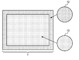
- FIG. 1A is a schematic cross-sectional view (schematic cross-sectional view taken along line 1A-1A in FIG. 1B) showing an example of the composite coil module of the present embodiment.
- FIG. 1B is a schematic plan view showing an example of a composite coil module.
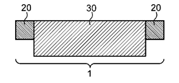
- FIG. 2A is a schematic plan view showing an example of a magnetic sheet used in the composite coil module of the present embodiment.
- FIG. 2B is a schematic cross-sectional view showing an example of a magnetic sheet used for the composite coil module.
- FIG. 3 is a schematic plan view showing an example of the first magnetic path forming portion and the second magnetic path forming portion of the magnetic sheet used in the composite coil module of the present embodiment.
- FIG. 4A is a schematic cross-sectional view showing an example of the shape of a slit provided in the magnetic sheet used in the composite coil module of the present embodiment.
- FIG. 4B is a schematic cross-sectional view showing an example of the shape of a slit provided in the magnetic sheet used in the composite coil module of the present embodiment.
- FIG. 5 is a schematic plan view showing another example of the first magnetic path forming portion and the second magnetic path forming portion of the magnetic sheet used in the composite coil module of the present embodiment.
- FIG. 6 is a schematic plan view showing another example of the first magnetic path forming portion and the second magnetic path forming portion of the magnetic sheet used in the composite coil module of the present embodiment.
- FIG. 7 is a schematic cross-sectional view showing another example of the first magnetic path forming portion and the second magnetic path forming portion of the magnetic sheet used in the composite coil module of the present embodiment.
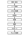
- FIG. 8 is a flowchart showing an example of the manufacturing process of the magnetic sheet in the present embodiment.
- FIG. 9 is a graph showing frequency characteristics of magnetic permeability ( ⁇ ′, ⁇ ′′) in a conventional Mn—Zn ferrite sheet (magnetic sheet).
- FIG. 10 is a graph showing the relationship between the slit pitch and the magnetic permeability of the magnetic sheet in this embodiment.
- FIG. 11 is a graph showing frequency characteristics of the Mn—Zn ferrite sheet (magnetic sheet) in the present embodiment.
- Patent Document 1 it is necessary to stack two types of magnetic sheets having different characteristics between an NFC antenna and a non-contact charging coil. Thereby, the subject that the process of producing a composite coil module becomes complicated arises, and also the subject that cost reduction of a composite coil module becomes difficult occurs.
- the present disclosure can simplify the manufacturing process of a composite coil module by modularizing and downsizing a wireless communication coil and a non-contact charging coil with a magnetic sheet made of one type of magnetic material.
- a composite coil module and a magnetic sheet that can reduce the cost of the module and can improve both the communication efficiency of wireless communication and the power transmission efficiency of non-contact charging with a magnetic sheet made of one kind of magnetic material.
- magnetic material the protective layer, and the antenna module described below are merely examples, and are not limited to the following configurations and materials.
- FIG. 1A and 1B show an example of the composite coil module of the present embodiment.
- FIG. 1A is a schematic cross-sectional view (schematic cross-sectional view taken along line 1A-1A in FIG. 1B) showing an example of the composite coil module
- FIG. 1B is a schematic plan view showing an example of the composite coil module.
- the composite coil module of this embodiment includes a substrate 5 and a magnetic sheet 1.
- substrate 5 has the 1st planar coil 2 of the at least 1 or more types used for short-distance wireless communication wound, and the 2nd planar coil 3 used for the electric power transmission of non-contact charge.
- the second planar coil 3 is used as a charging coil, and the first planar coil 2 disposed so as to surround the charging coil is an antenna for short-range wireless communication.
- the first planar coil 2 and the second planar coil 3 formed on the substrate 5 are joined to the magnetic sheet 1 via the adhesive layer 6.
- the substrate 5 can be formed of a flexible insulating film.
- the insulating film include polyimide, PET (polyethylene terephthalate), glass epoxy (glass epoxy) substrate, and FPC (flexible printed circuit board).
- a thin and flexible antenna module can be manufactured by using polyimide, PET, or the like as a substrate. In the embodiment, for example, it is preferable to use a polyimide film having a thickness of 10 ⁇ m to 200 ⁇ m.
- the first planar coil 2 performs short-range wireless communication, for example, by electromagnetic induction using a specific frequency band called RFID.
- a specific frequency band called RFID for example, in the case of NFC (Near Field Communication), a frequency of 13.56 MHz can be used.
- An NFC antenna is an antenna that performs communication by electromagnetic induction using a frequency of 13.56 MHz, and a sheet antenna is generally used.
- the second planar coil 3 can be contactlessly charged by electromagnetic induction using a frequency of about 100 to 200 kHz according to standards such as WPC (Wireless Power Consortium), PMA (Power Matters Alliance), and A4WP (Alliance for Wireless Power). It is what is called a charging coil that performs the power transmission.
- the charging coil is formed by plating a copper foil having a line width of about 800 ⁇ m and a thickness of about 60 ⁇ m with two terminals at the start and end, and is wound so as to draw a vortex on the surface around the hollow portion. Has been.
- the first planar coil 2 and the second planar coil 3 are usually wound.
- a specific example of how to wind the first planar coil and the second planar coil includes so-called ⁇ winding, but is not limited to this winding method, and is not limited to a substantially rectangular shape, including a substantially rectangular shape, a substantially square shape, an elliptical shape, a polygonal shape, or the like. Any shape is acceptable.
- the number of turns of the first planar coil and the second planar coil is three, but the number of turns is not limited to this. There are no particular restrictions on the material, height and width of the conductors constituting each of the first planar coil 2 and the second planar coil 3 and the gap between adjacent conductors.
- a metal foil such as copper foil can be used as the material of the conductor, and the height of the conductor, that is, the thickness of the first planar coil 2 and the second planar coil 3 is about 70 ⁇ m or more and 80 ⁇ m or less. Good.
- the single substrate has both the first planar coil 2 and the second planar coil 3, it is possible to realize multi-function and downsizing.
- One planar coil of the first planar coil 2 and the second planar coil 3 is provided inside the other planar coil.
- the form in which the first planar coil 2 is provided inside the second planar coil 3 may be used.
- the second planar coil 3 to be performed is provided on the inner side and the first planar coil 2 for performing short-range wireless communication is provided on the outer side. Therefore, the following composite coil module demonstrates the form of the 1st plane coil 2 provided so that the 2nd plane coil 3 might be enclosed.
- the front and back of the substrate 5 are defined as a first surface and a second surface, respectively.
- the substrate 5 is provided with a through hole.
- a second planar coil 3 is provided on the first surface and the second surface of the substrate 5 so as to surround the periphery of the through hole.
- the second planar coil 3 is electrically connected through a plated through hole.
- a protective layer 4 is provided on the first surface and the second surface of the substrate to protect the second planar coil.
- the protective layer include a cured product of a liquid solder resist, a solder resist film, or a coverlay.
- the protective layer 4 may or may not be provided.
- the second planar coil 3 may be provided on both the first surface and the second surface of the substrate 5 (two-layer structure), and is provided on one side of the first surface or the second surface of the substrate. Also good (single layer structure).
- the first planar coil 2 is provided on the second surface of the substrate so as to surround the periphery of the second planar coil 3. If the first planar coil 2 is provided on both sides of the substrate, radio wave interference may occur. Therefore, the first planar coil 2 is preferably provided on one side of the substrate 5. In the composite coil module shown in FIG. 1A, the first planar coil 2 is provided on the second surface of the substrate 5.
- the magnetic sheet 1 which is one of the major features of this embodiment, will be specifically described with reference to FIGS. 2A and 2B.
- the magnetic sheet used for the composite coil module is described.
- the magnetic sheet of the present embodiment is not limited to this and can be widely used for other purposes.
- FIG. 2A is a schematic plan view of a magnetic sheet used in the composite coil module of this embodiment
- FIG. 2B is a schematic cross-sectional view of the magnetic sheet (schematic cross-sectional view taken along line 2B-2B in FIG. 2A).
- the magnetic sheet 1 of the present embodiment is made of one type of magnetic material that forms the magnetic path of the first planar coil and the magnetic path of the second planar coil.
- the magnetic sheet 1 includes a first magnetic path forming portion (first portion) 20 in which the magnetic path of the first planar coil is formed, and a second magnetic path of the second planar coil. And a magnetic path forming part (second part) 30.
- the frequency characteristics are arbitrarily changed in one magnetic sheet made of one type of magnetic material, so that the communication efficiency of the first planar coil and the power transmission efficiency of the non-contact charging in the second planar coil can be improved. Both can be satisfied.
- the first magnetic path forming part (first part) 20 and the second magnetic path forming part (second part) 30 are designed to have different magnetic permeability.
- the magnetic sheet 1 composed of the first magnetic path forming portion 20 and the second magnetic path forming portion 30 may have protective layers 4 on the front side and the back side, respectively.
- the protective layer 4 an ultraviolet curable resin, a visible light curable resin, a thermoplastic resin, a thermosetting resin, a heat resistant resin, a synthetic rubber, a double-sided tape, an adhesive layer, a film, or the like can be used.
- the protective layer 4 may not be provided.
- the magnetic sheet 1 made of one kind of magnetic material examples of means for arbitrarily changing the frequency characteristics between the first magnetic path forming unit 20 and the second magnetic path forming unit 30 are shown in FIGS. 2A and 2B.
- the magnetic sheet has slits or dots, and the distance (roughness) between the slits or dots of the first magnetic path forming unit 20 is the distance between the slits or dots of the second magnetic path forming unit 30. It can be made smaller (coarse) than (roughness).
- the magnetic sheet 1 having a location dependency on the magnetic permeability can be obtained.
- the slit indicates a slit-shaped concave portion
- the dot indicates a dot-shaped concave portion.
- the slit-like recess and the dot-like recess may be collectively referred to as a recess.
- the recess may have a hole shape penetrating from the front surface to the back surface of the magnetic sheet.
- a slit is provided in the first magnetic path forming portion (portion placed on the NFC antenna) 8.
- the magnetic permeability varies depending on the location.
- a sheet can be obtained.
- the magnetic sheet 1 of the first magnetic path forming portion 8 has flexibility
- the magnetic sheet 1 of the second magnetic path forming portion 9 has almost no flexibility, and the magnetic sheet made of one kind of magnetic material. 1, the magnetic permeability can be changed.
- the distance between the slits or dots formed in the second magnetic path forming unit 9 is preferably 100 mm or less.
- the pitch here refers to the interval between the slits formed in the vertical and horizontal directions on the magnetic sheet. This refers to a value measured by, for example, an optical microscope or a laser shape microscope. More specifically, for example, using a VK-X150 manufactured by Keyence as a laser shape microscope, the magnetic sheet is set on the microscope and the magnification is adjusted to measure the interval between the slits formed on the magnetic sheet. Is possible.
- the shape of the array is not limited as long as it has a constant interval (pitch) as described above between a plurality of slits or a plurality of dots.
- the entire surface of the magnetic sheet 1 is uniform.
- the pitch of the slits or dots of the first magnetic path forming unit 8 is more preferably 0.05 mm or more and 5 mm or less, and the pitch of the slits or dots of the second magnetic path forming unit 9 is more preferably 5 mm or more and 20 mm or less. is there.
- the shape of the slit or dot is not particularly limited.
- the slit or the dot may be a cut shape as shown in FIG. 4A or a through-hole, but for the reason of preventing the occurrence of waviness at the edge of the thin magnetic material, FIG. It is preferable that it is a recessed part provided with a bottom part as shown in.
- the depth of the slit or dot in the present embodiment is not particularly limited, but is preferably 5% or more and 30% or less (about 5 ⁇ m or more and 30 ⁇ m or less) with respect to the thickness d1 (about 100 ⁇ m) of the magnetic material. Is preferred). If the slit or the dot has a depth in such a range, there is an advantage that the magnetic material can be easily formed by a break treatment described later and the magnetic material can be formed flat.
- the magnetic sheet 1 is divided into small pieces by a break process described later using the slits or dots.
- the slit or dot processing is generally formed linearly, but may be bent or formed in a curved shape.
- the first magnetic path forming unit 10 is made of the magnetic sheet 1 made of one type of magnetic material as shown in FIG.
- An elastic silicone resin is contained, and the second magnetic path forming unit 11 may contain an epoxy resin.
- an elastic silicone resin is applied to the first magnetic path forming unit 10 on the magnetic sheet 1 (elastic silicone applied part), and the second magnetic path forming unit 11 is applied to the second magnetic path forming unit 11.
- an elastic silicone resin used by this embodiment, A commercially available thing can be used. Preferable specific examples include TSE322-B from Momentive.
- the epoxy resin is not particularly limited, but a preferable epoxy resin includes 2206 manufactured by Three Bond Co., Ltd.
- the first magnetic path forming unit 12 sets the particle size of the magnetic material to less than 5 mm, and the second magnetic path.
- the forming unit 13 changes the magnetic permeability of the magnetic sheet 1 by making the particle size of the magnetic material 5 mm or more, thereby causing a difference in the particle size of the magnetic material in the magnetic sheet 1 made of one kind of magnetic material. be able to.
- the more preferable particle diameter of the magnetic material is about 0.05 mm or more and 5 mm or less in the first magnetic path forming unit 12 and about 5 mm or more and 20 mm or less in the second magnetic path forming unit.
- the particle size of the magnetic material is a small piece of the magnetic material generated by a break process, which will be described later, and is a value measured by an optical microscope, a laser shape microscope, or the like. More specifically, for example, using a VK-X150 manufactured by Keyence Corporation as a laser shape microscope, the particle size can be measured by setting a magnetic material on the microscope and adjusting the magnification.
- the thickness of the magnetic sheet forming the first magnetic path forming portion is made thinner than the thickness of the magnetic sheet forming the second magnetic path forming portion.
- the first magnetic path forming unit 20 sets the thickness of the magnetic sheet to 50 ⁇ m or more and 200 ⁇ m or less, and forms the second magnetic path.
- the part 30 can change the magnetic permeability of the magnetic sheet 1 by adjusting the thickness of the magnetic sheet to 200 ⁇ m or more and 500 ⁇ m or less to cause a difference in the break state in the magnetic sheet 1 made of one kind of magnetic material. it can.
- the method for adjusting the thickness of the magnetic sheet 1 can be performed by a known means without any particular limitation, and examples thereof include a method in which only the first magnetic path forming portion 20 is cut and thinned to have a desired thickness.
- a difference is provided between the firing temperature of the first magnetic path forming unit 20 and the firing temperature of the second magnetic path forming unit 30 at the time of manufacture.
- a magnetic permeability difference between the part placed on the antenna and the part placed on the non-contact charging coil unit can be generated, and the NFC communication efficiency and non-efficiency can be achieved with the magnetic sheet 1 made of one kind of magnetic substance. It is considered that both the power transfer efficiency of contact charging can be satisfied.
- a difference in frequency characteristics can be generated between the first magnetic path forming unit 20 and the second magnetic path forming unit 30 in the magnetic sheet 1 made of one kind of magnetic material.
- the magnetic sheet 1 of the present embodiment has a magnetic permeability (first magnetic permeability) at the first magnetic path forming portion (first portion) 20 and a magnetic permeability at the second magnetic path forming portion (second portion) 30.
- the magnetic sheet 1 of the present embodiment includes a first magnetic path forming part (first portion) 20 in which the magnetic path of the first planar coil is formed, and a second magnet in which the magnetic path of the second planar coil is formed.
- the magnetic permeability (first magnetic permeability) at the first magnetic path forming part (first part) 20 and the magnetic permeability (second magnetic permeability) at the second magnetic path forming part (second part) 30 ) can be designed to have a third magnetic permeability different from that of the third magnetic path forming portion (third portion).
- the magnetic body used in the present embodiment is a ferrite sintered body, specifically, a Mn—Zn ferrite, and depending on the application, a Ni—Zn ferrite, a Mn—Ni ferrite, a Mg—Zn ferrite. Etc. can be used. Further, it may be a magnetic material such as amorphous metal, permalloy, electromagnetic steel, silicon iron, Fe—Al alloy, or Sendust alloy. Furthermore, a magnetic material may be contained in a sheet-like resin material.
- the magnetic body of the present embodiment is in the form of a sheet and preferably has a thickness of about 50 ⁇ m to 1000 ⁇ m.
- the protective layer 4 used in the present embodiment is preferably insulative and has flexibility, for example, a plastic film such as PET (polyethylene terephthalate) having an adhesive layer.
- This protective layer maintains the magnetic material divided into small pieces in a sheet shape so that the magnetic material of the small pieces is not spilled or damaged.
- the upper and lower surfaces of the magnetic sheet may be bonded with a PET film, and at least one surface is protected.
- a protective layer may be formed by applying an elastic silicone resin / epoxy resin as shown in FIG. -UV curable resin can also be used.
- an FPC Flexible Printed Circuits
- the protective layer may be selected in consideration of weather resistance of heat resistance and moisture resistance as well as flexibility for bending and bending of each component constituting the composite coil module.
- FIG. 8 is a manufacturing process flow chart of the magnetic sheet in the present embodiment.
- a manufacturing flow of a ferrite sheet will be described as an example of the magnetic sheet of the present embodiment.
- the magnetic sheet of this embodiment for example, as shown in the flow in FIG. 8, by performing material blending / mixing ⁇ sheet molding ⁇ slit processing ⁇ die cutting ⁇ desorption ⁇ firing ⁇ laminating ⁇ breaking processing, Obtainable. Each step will be described in detail.
- a ferrite powder and a polyvinyl butyral resin or phthalate ester plasticizer as a binder and an organic solvent are blended, and then kneaded in a dedicated mill to produce a slurry.
- the viscosity of the prepared slurry is not particularly limited as long as it is a suitable viscosity for sheet molding. For example, it is preferably about 1500 Pa ⁇ sec to 2500 Pa ⁇ sec at 20 ° C.
- the sheet molding is performed by forming the ferrite slurry prepared as described above using a doctor blade on a support such as a PET film and performing a heat drying treatment in a thermostatic bath. Thereby, a green sheet having a thickness of 50 ⁇ m or more and 350 ⁇ m or less is manufactured.
- green sheets can be formed by an extrusion molding machine.
- a plurality of slits or dots are formed on at least one of the upper and lower surfaces of the green sheet thus produced.
- the magnetic permeability difference of the magnetic body of the part mounted in the NFC antenna and the part mounted in the non-contact charging coil part can be produced on one magnetic sheet.
- this slit process can also be replaced with other means for changing the magnetic permeability described above.
- the formation of the slits or dots is not particularly limited, but can be performed, for example, by rotating a roller in which a plurality of convex portions are regularly arranged at a desired pitch while pressing on the green sheet. As a result, the plurality of convex portions enter the inside of the green sheet, and a plurality of slits or dots are formed on the green sheet.
- the green sheet produced by the above procedure is die-cut into a certain dimensional shape with a laser or pinnacle.
- the green sheet thus punched out removes the solvent as a binder in a temperature pattern under a predetermined condition (desolvation).
- the temperature at which the solvent is removed is not particularly limited, and can be set as appropriate depending on the type and amount of the organic solvent.
- firing is performed at a predetermined temperature in a firing furnace (firing).
- the firing temperature is not particularly limited, and can be appropriately set depending on the type of ferrite.
- the fired magnetic body is coated with a PET film or the like on the upper and lower surfaces of the magnetic body by an automatic machine to form a protective layer.
- a magnetic sheet having protective layers made of PET film formed on the upper and lower surfaces of the magnetic material is pressed from both the vertical and horizontal directions with a cylindrical rigid body (break treatment).
- break treatment a cylindrical rigid body
- the magnetic sheet of this embodiment can be created.
- the relative permeability of the sintered ferrite body is represented by the following complex permeability.
- ⁇ ⁇ ′ ⁇ j ⁇ ′′ ( ⁇ : relative permeability, ⁇ ′: inductance component, ⁇ ′′: resistance component)
- the permeability of the ferrite has a constant value up to a certain frequency, but as the frequency increases, a phase delay occurs and ⁇ ′ (inductance component) decreases and ⁇ ′′ (resistance component) ) Is increasing, and this is called the snake limit.
- the conventional Mn—Zn ferrite material has high magnetic permeability at 100 kHz to 200 kHz and can be used for non-contact charging because of high power transmission efficiency of non-contact charging, but the 13.56 MHz band used for the NFC antenna.
- ⁇ ′ inductance component
- ⁇ ′′ resistance component
- Mn-Zn ferrite is used for the non-contact charging part and Ni-Zn ferrite is used for the NFC antenna part, and two different types of ferrite materials are used. It was inevitable.
- a magnetic sheet in which a slit having a thickness of 80 ⁇ m and a depth of 10% with respect to the thickness d1 of the magnetic material is formed using the Mn—Zn ferrite material by the manufacturing method as described above.
- the permeability was measured by changing the slit pitch, it was found that the graph shown in FIG. 10 was obtained.
- the ferrite material can arbitrarily change ⁇ ′ (inductance component) and ⁇ ′′ (resistance component) of the ferrite material by changing the slit pitch in various ways. Specifically, it has been found that the permeability ( ⁇ ) increases as the slit pitch increases.
- the slit pitch of the magnetic sheet is changed between the part placed on the NFC antenna and the part placed on the non-contact charging coil part in the magnetic sheet made of one kind of magnetic material.
- the distance between the slits it was possible to arbitrarily change the inductance component and the resistance component of the magnetic permeability of the magnetic sheet made of one kind of magnetic material.
- the permeability ( ⁇ ) increases as the slit pitch interval increases (coarse).
- FIG. 11 it was found that a magnetic sheet capable of sufficiently satisfying the characteristics can be obtained in the non-contact charging 100 kHz band and the NFC antenna 13.56 MHz band.
- the NFC antenna and the non-contact charging coil are modularized by a magnetic sheet made of one kind of magnetic material, thereby reducing the size of the composite coil module and simplifying the manufacturing process. Therefore, the cost of the composite coil module can be reduced. In addition, there is an effect that both the NFC communication efficiency and the power transmission efficiency of non-contact charging can be improved with a magnetic sheet made of one kind of magnetic material.
- the magnetic sheet of the present embodiment can be used for various applications such as an antenna device, a mobile phone equipped with a non-contact charging module, a digital camera, a portable terminal such as a notebook PC, a module of a non-contact charging system for electronic devices, and the like. .
- the magnetic sheet of this embodiment can be used for battery charging of an electric vehicle. Normally, when charging the battery of an electric vehicle, the charging performance is significantly impaired by eddy current generated by the metal of the vehicle body, but by using the magnetic sheet of this embodiment, adverse effects such as eddy current loss are suppressed. The advantage that desired charging performance can be realized is exhibited.
- the composite coil module according to the present disclosure is configured by placing a wound charging coil and an NFC antenna disposed so as to surround the charging coil on a magnetic sheet made of one kind of magnetic material, and a non-contact charging coil unit and an NFC By arbitrarily changing the frequency characteristic of the magnetic sheet made of one kind of magnetic material placed on the antenna unit, both the communication efficiency in NFC and the power transmission efficiency of contactless charging can be satisfied. Moreover, the magnetic sheet of this indication can be used for said composite coil module.
- an NFC antenna and a non-contact charging coil with a magnetic sheet made of one type of magnetic material it is possible to reduce the size of the composite coil module and simplify the manufacturing process, and to reduce the cost of the composite coil module. Is possible. Therefore, the present disclosure is extremely useful for various electronic devices such as an antenna device including an NFC antenna and a contactless charging coil, a portable terminal, particularly a smartphone, a portable audio, a personal computer, a digital camera, and a video camera.
- Magnetic sheet 2 First planar coil (NFC antenna) 3 Second planar coil (non-contact charging coil) 4 Protective layer 5 Substrate 6
- Adhesive layer 8 20 First magnetic path forming part (first part) 9, 30 Second magnetic path forming part (second part) 10 1st magnetic path formation part (elastic silicone application part) 11 Second magnetic path forming part (epoxy resin application part) 12 1st magnetic path formation part (part with small ferrite particle size) 13 Second magnetic path forming part (part with large ferrite grain size)
Abstract
Description
μ=μ’-jμ’’(μ:比透磁率、μ’:インダクタンス成分、μ’’:抵抗成分)
図9に示されているように、フェライトの透磁率はある周波数までは一定の値をとるが、周波数が高くなると位相の遅れが生じμ’(インダクタンス成分)が減少し、μ”(抵抗成分)が増加してくる現象があり、これをスネークの限界と呼んでいる。 By the way, as is well known, the relative permeability of the sintered ferrite body is represented by the following complex permeability.
μ = μ′−jμ ″ (μ: relative permeability, μ ′: inductance component, μ ″: resistance component)
As shown in FIG. 9, the permeability of the ferrite has a constant value up to a certain frequency, but as the frequency increases, a phase delay occurs and μ ′ (inductance component) decreases and μ ″ (resistance component) ) Is increasing, and this is called the snake limit.
2 第1平面コイル(NFCアンテナ部)
3 第2平面コイル(非接触充電コイル部)
4 保護層
5 基板
6 接着層
8,20 第1磁路形成部(第1部分)
9,30 第2磁路形成部(第2部分)
10 第1磁路形成部(弾性シリコーン塗布部分)
11 第2磁路形成部(エポキシ樹脂塗布部分)
12 第1磁路形成部(フェライト粒径の小さい部分)
13 第2磁路形成部(フェライト粒径の大きい部分) 1
3 Second planar coil (non-contact charging coil)
4
9, 30 Second magnetic path forming part (second part)
10 1st magnetic path formation part (elastic silicone application part)
11 Second magnetic path forming part (epoxy resin application part)
12 1st magnetic path formation part (part with small ferrite particle size)
13 Second magnetic path forming part (part with large ferrite grain size)
Claims (19)
- 無線通信に用いられる第1平面コイルと、
非接触充電の電力伝送に用いられる第2平面コイルと、
前記第1平面コイルの磁路及び前記第2平面コイルの磁路が形成される1種類の磁性体からなる磁性シートを備え、
前記磁性シートは、前記第1平面コイルの前記磁路が形成される第1磁路形成部と、前記第2平面コイルの前記磁路が形成される第2磁路形成部とを有し、
前記第1磁路形成部の透磁率は、前記第2磁路形成部の透磁率と異なる、複合コイルモジュール。 A first planar coil used for wireless communication;
A second planar coil used for non-contact charging power transmission;
Comprising a magnetic sheet made of one kind of magnetic material on which the magnetic path of the first planar coil and the magnetic path of the second planar coil are formed;
The magnetic sheet has a first magnetic path forming portion in which the magnetic path of the first planar coil is formed, and a second magnetic path forming portion in which the magnetic path of the second planar coil is formed,
The composite coil module, wherein the magnetic permeability of the first magnetic path forming portion is different from the magnetic permeability of the second magnetic path forming portion. - 前記磁性シートは、複数の凹部を有し、
前記第1磁路形成部における前記複数の凹部間の距離が、前記第2磁路形成部における前記複数の凹部間の距離より小さい、請求項1に記載の複合コイルモジュール。 The magnetic sheet has a plurality of recesses,
2. The composite coil module according to claim 1, wherein a distance between the plurality of recesses in the first magnetic path forming portion is smaller than a distance between the plurality of recesses in the second magnetic path forming portion. - 前記第1磁路形成部における前記複数の凹部間の距離が、0mm以上5mm以下のピッチであり、
前記第2磁路形成部における前記複数の凹部間の距離が、20mm以上のピッチである、請求項2に記載の複合コイルモジュール。 The distance between the plurality of recesses in the first magnetic path forming portion is a pitch of 0 mm or more and 5 mm or less,
The composite coil module according to claim 2, wherein a distance between the plurality of recesses in the second magnetic path forming portion is a pitch of 20 mm or more. - 前記第1磁路形成部は、前記第2磁路形成部よりもフレキシブルである、請求項1~3のいずれかに記載の複合コイルモジュール。 The composite coil module according to any one of claims 1 to 3, wherein the first magnetic path forming portion is more flexible than the second magnetic path forming portion.
- 前記第1磁路形成部は、弾性シリコーン系樹脂を含み、
前記第2磁路形成部は、エポキシ系樹脂を含む、請求項1または2に記載の複合コイルモジュール。 The first magnetic path forming portion includes an elastic silicone resin,
The composite coil module according to claim 1, wherein the second magnetic path forming unit includes an epoxy resin. - 前記第1磁路形成部における前記磁性体の粒径は、前記第2磁路形成部における前記磁性体の粒径よりも小さい、請求項1または2に記載の複合コイルモジュール。 The composite coil module according to claim 1 or 2, wherein a particle diameter of the magnetic body in the first magnetic path forming portion is smaller than a particle diameter of the magnetic body in the second magnetic path forming portion.
- 前記第1磁路形成部における前記磁性シートの厚みは、前記第2磁路形成部における前記磁性シートの厚みよりも薄い、請求項1または2に記載の複合コイルモジュール。 The composite coil module according to claim 1 or 2, wherein a thickness of the magnetic sheet in the first magnetic path forming portion is thinner than a thickness of the magnetic sheet in the second magnetic path forming portion.
- 前記磁性体は、Mn-Zn系フェライトである、請求項1~7のいずれかに記載の複合コイルモジュール。 The composite coil module according to any one of claims 1 to 7, wherein the magnetic body is Mn-Zn ferrite.
- 前記複数の凹部は、複数のスリット状の凹部、または、複数のドット状の凹部である、請求項2または3に記載の複合コイルモジュール。 The composite coil module according to claim 2 or 3, wherein the plurality of recesses are a plurality of slit-like recesses or a plurality of dot-like recesses.
- 1種類の磁性体からなる磁性シートであって、第1透磁率を有する第1部分と、前記第1透磁率とは異なる第2透磁率を有する第2部分を有する、磁性シート。 A magnetic sheet made of a single type of magnetic material, having a first portion having a first magnetic permeability and a second portion having a second magnetic permeability different from the first magnetic permeability.
- 複数の凹部を有し、前記第1部分における前記複数の凹部間の距離は、前記第2部分における前記複数の凹部間の距離と異なっている、請求項10に記載の磁性シート。 The magnetic sheet according to claim 10, comprising a plurality of recesses, wherein a distance between the plurality of recesses in the first part is different from a distance between the plurality of recesses in the second part.
- 前記第1部分における前記複数の凹部間の距離が0mm以上5mm以下のピッチであり、
前記第2部分における前記複数の凹部間の距離が20mm以上のピッチである、請求項11に記載の磁性シート。 The distance between the plurality of recesses in the first portion is a pitch of 0 mm or more and 5 mm or less,
The magnetic sheet according to claim 11, wherein a distance between the plurality of recesses in the second portion is a pitch of 20 mm or more. - 前記第1部分は、前記第2部分よりもフレキシブルである、請求項10~12のいずれかに記載の磁性シート。 The magnetic sheet according to any one of claims 10 to 12, wherein the first portion is more flexible than the second portion.
- 前記第1部分は、弾性シリコーン系樹脂を含み、
前記第2部分は、エポキシ系樹脂を含む、請求項10または11に記載の磁性シート。 The first portion includes an elastic silicone resin,
The magnetic sheet according to claim 10 or 11, wherein the second portion includes an epoxy resin. - 前記第1部分における前記磁性体の粒径は、前記第2部分における前記磁性体の粒径よりも小さい、請求項10または11に記載の磁性シート。 The magnetic sheet according to claim 10 or 11, wherein a particle diameter of the magnetic body in the first portion is smaller than a particle diameter of the magnetic body in the second portion.
- 前記第1部分における前記磁性シートの厚みは、前記第2部分における前記磁性シートの厚みよりも薄い、請求項10または11に記載の磁性シート。 The magnetic sheet according to claim 10 or 11, wherein a thickness of the magnetic sheet in the first portion is thinner than a thickness of the magnetic sheet in the second portion.
- 前記磁性体は、Mn-Zn系フェライトである、請求項10~16のいずれかに記載の磁性シート。 The magnetic sheet according to any one of claims 10 to 16, wherein the magnetic body is Mn-Zn ferrite.
- 前記第1透磁率および前記第2透磁率とは異なる第3透磁率を有する第3部分をさらに有する、請求項10~17のいずれかに記載の磁性シート。 The magnetic sheet according to any one of claims 10 to 17, further comprising a third portion having a third magnetic permeability different from the first magnetic permeability and the second magnetic permeability.
- 前記複数の凹部は、複数のスリット状の凹部、または、複数のドット状の凹部である、請求項11または12に記載の磁性シート。 The magnetic sheet according to claim 11 or 12, wherein the plurality of recesses are a plurality of slit-like recesses or a plurality of dot-like recesses.
Priority Applications (4)
| Application Number | Priority Date | Filing Date | Title |
|---|---|---|---|
| JP2018553735A JPWO2018100975A1 (en) | 2016-11-29 | 2017-11-07 | Composite coil module and magnetic sheet |
| US16/461,416 US20190348203A1 (en) | 2016-11-29 | 2017-11-07 | Combined coil module and magnetic sheet |
| CN201780073207.3A CN109997205A (en) | 2016-11-29 | 2017-11-07 | Compound coil module and magnetic piece |
| KR1020197015002A KR20190085941A (en) | 2016-11-29 | 2017-11-07 | Composite coil module and magnetic sheet |
Applications Claiming Priority (4)
| Application Number | Priority Date | Filing Date | Title |
|---|---|---|---|
| JP2016231034 | 2016-11-29 | ||
| JP2016-231034 | 2016-11-29 | ||
| JP2016231029 | 2016-11-29 | ||
| JP2016-231029 | 2016-11-29 |
Publications (1)
| Publication Number | Publication Date |
|---|---|
| WO2018100975A1 true WO2018100975A1 (en) | 2018-06-07 |
Family
ID=62242833
Family Applications (1)
| Application Number | Title | Priority Date | Filing Date |
|---|---|---|---|
| PCT/JP2017/040028 WO2018100975A1 (en) | 2016-11-29 | 2017-11-07 | Combined coil module and magnetic sheet |
Country Status (5)
| Country | Link |
|---|---|
| US (1) | US20190348203A1 (en) |
| JP (1) | JPWO2018100975A1 (en) |
| KR (1) | KR20190085941A (en) |
| CN (1) | CN109997205A (en) |
| WO (1) | WO2018100975A1 (en) |
Cited By (3)
| Publication number | Priority date | Publication date | Assignee | Title |
|---|---|---|---|---|
| WO2020068389A1 (en) * | 2018-09-27 | 2020-04-02 | Apple Inc. | Dual mode wireless power system designs |
| WO2020171619A1 (en) | 2019-02-20 | 2020-08-27 | Samsung Electronics Co., Ltd. | Electronic device including flexible printed circuit board laminated wireless charging coil and near field communication antenna pattern |
| WO2020259660A1 (en) * | 2019-06-28 | 2020-12-30 | 华为技术有限公司 | Touch panel with nfc function, and terminal device |
Families Citing this family (3)
| Publication number | Priority date | Publication date | Assignee | Title |
|---|---|---|---|---|
| US11365691B2 (en) * | 2019-09-05 | 2022-06-21 | Pratt & Whitney Canada Corp. | Blade angle position feedback system with embedded markers |
| JP7428098B2 (en) * | 2020-07-31 | 2024-02-06 | Tdk株式会社 | Inductor parts and DC/DC converters using the same |
| CN112712957B (en) * | 2020-12-24 | 2021-08-17 | 深圳市驭能科技有限公司 | Nanocrystalline magnetic conductive sheet for wireless charging and near field communication and preparation method thereof |
Citations (4)
| Publication number | Priority date | Publication date | Assignee | Title |
|---|---|---|---|---|
| WO2008126690A1 (en) * | 2007-03-29 | 2008-10-23 | Kabushiki Kaisha Asahi Rubber | Electromagnetic shield sheet and rfid plate |
| JP2008296431A (en) * | 2007-05-30 | 2008-12-11 | Kitagawa Ind Co Ltd | Ceramic sheet |
| JP2013121248A (en) * | 2011-12-07 | 2013-06-17 | Panasonic Corp | Non-contact charging module and mobile terminal comprising the same |
| JP2014183469A (en) * | 2013-03-19 | 2014-09-29 | Dexerials Corp | Antenna device and electronic equipment |
Family Cites Families (5)
| Publication number | Priority date | Publication date | Assignee | Title |
|---|---|---|---|---|
| KR101187172B1 (en) * | 2007-03-07 | 2012-09-28 | 도다 고교 가부시끼가이샤 | Ferrite Molded Sheet, Sintered Ferrite Substrate and Antenna Module |
| JP5219975B2 (en) * | 2009-09-30 | 2013-06-26 | パナソニック株式会社 | Coil and transformer |
| US9515492B2 (en) * | 2012-12-06 | 2016-12-06 | Toyota Motor Engineering & Manufacturing North America, Inc. | Wireless power transfer using air gap and metamaterial |
| JP2016181620A (en) * | 2015-03-24 | 2016-10-13 | 三菱電機株式会社 | Magnetic core for current transformer, current transformer and watthour meter |
| US10658847B2 (en) * | 2015-08-07 | 2020-05-19 | Nucurrent, Inc. | Method of providing a single structure multi mode antenna for wireless power transmission using magnetic field coupling |
-
2017
- 2017-11-07 CN CN201780073207.3A patent/CN109997205A/en active Pending
- 2017-11-07 US US16/461,416 patent/US20190348203A1/en not_active Abandoned
- 2017-11-07 JP JP2018553735A patent/JPWO2018100975A1/en active Pending
- 2017-11-07 KR KR1020197015002A patent/KR20190085941A/en unknown
- 2017-11-07 WO PCT/JP2017/040028 patent/WO2018100975A1/en active Application Filing
Patent Citations (4)
| Publication number | Priority date | Publication date | Assignee | Title |
|---|---|---|---|---|
| WO2008126690A1 (en) * | 2007-03-29 | 2008-10-23 | Kabushiki Kaisha Asahi Rubber | Electromagnetic shield sheet and rfid plate |
| JP2008296431A (en) * | 2007-05-30 | 2008-12-11 | Kitagawa Ind Co Ltd | Ceramic sheet |
| JP2013121248A (en) * | 2011-12-07 | 2013-06-17 | Panasonic Corp | Non-contact charging module and mobile terminal comprising the same |
| JP2014183469A (en) * | 2013-03-19 | 2014-09-29 | Dexerials Corp | Antenna device and electronic equipment |
Cited By (10)
| Publication number | Priority date | Publication date | Assignee | Title |
|---|---|---|---|---|
| WO2020068389A1 (en) * | 2018-09-27 | 2020-04-02 | Apple Inc. | Dual mode wireless power system designs |
| US11515083B2 (en) | 2018-09-27 | 2022-11-29 | Apple Inc. | Dual mode wireless power system designs |
| US11887775B2 (en) | 2018-09-27 | 2024-01-30 | Apple Inc. | Dual mode wireless power system designs |
| WO2020171619A1 (en) | 2019-02-20 | 2020-08-27 | Samsung Electronics Co., Ltd. | Electronic device including flexible printed circuit board laminated wireless charging coil and near field communication antenna pattern |
| KR20200101809A (en) * | 2019-02-20 | 2020-08-28 | 삼성전자주식회사 | An electronic device including flexible printed circuit board laminated wireless charging coil and near field communication antenna pattern |
| CN113454653A (en) * | 2019-02-20 | 2021-09-28 | 三星电子株式会社 | Electronic device including flexible printed circuit board laminated with wireless charging coil and near field communication antenna pattern |
| EP3888009A4 (en) * | 2019-02-20 | 2022-01-12 | Samsung Electronics Co., Ltd. | Electronic device including flexible printed circuit board laminated wireless charging coil and near field communication antenna pattern |
| US11665818B2 (en) | 2019-02-20 | 2023-05-30 | Samsung Electronics Co., Ltd. | Electronic device including flexible printed circuit board laminated wireless charging coil and near field communication antenna pattern |
| KR102580699B1 (en) * | 2019-02-20 | 2023-09-20 | 삼성전자주식회사 | An electronic device including flexible printed circuit board laminated wireless charging coil and near field communication antenna pattern |
| WO2020259660A1 (en) * | 2019-06-28 | 2020-12-30 | 华为技术有限公司 | Touch panel with nfc function, and terminal device |
Also Published As
| Publication number | Publication date |
|---|---|
| KR20190085941A (en) | 2019-07-19 |
| CN109997205A (en) | 2019-07-09 |
| JPWO2018100975A1 (en) | 2019-10-17 |
| US20190348203A1 (en) | 2019-11-14 |
Similar Documents
| Publication | Publication Date | Title |
|---|---|---|
| WO2018100975A1 (en) | Combined coil module and magnetic sheet | |
| US10658870B2 (en) | Combo antenna unit and wireless power receiving module comprising same | |
| CN108184333B (en) | Combined antenna module | |
| US10475571B2 (en) | Wireless power reception module | |
| TWI464964B (en) | Magnetic sheet, antenna module, electronic apparatus, and magnetic sheet manufacturing method | |
| KR101942149B1 (en) | Multi-coil module and electronic device | |
| JP5029371B2 (en) | Antenna device and adjustment method thereof | |
| US11087912B2 (en) | Magnetic field shield sheet for wireless power transmission and wireless power receiving module comprising same | |
| US10477743B2 (en) | Magnetic field shielding sheet and wireless power transmitting module including same | |
| CN108292804B (en) | Multifunctional composite module and portable equipment comprising same | |
| KR101795546B1 (en) | Shielding unit for a wireless charging and wireless power transfer module including the same | |
| KR101646492B1 (en) | A wireless charging module and shielding sheet for wireless charging apparatus | |
| EP2752943A1 (en) | Soft magnetic layer, receiving antenna, and wireless power receiving apparatus comprising the same | |
| KR102400391B1 (en) | Shielding unit for combo antenna and wireless charging module having the same | |
| KR102034231B1 (en) | Receiving antennas and wireless power receiving apparatus comprising the same | |
| WO2019111848A1 (en) | Coil module | |
| JP5136710B1 (en) | Manufacturing method of magnetic sheet | |
| JP2013149824A (en) | Manufacturing method of ferrite sheet | |
| JP5206886B1 (en) | Magnetic sheet and antenna device using the same | |
| JP2010147912A (en) | Antenna module, and manufacturing method thereof | |
| JP2013229550A (en) | Magnetic sheet | |
| KR20160097171A (en) | A wireless charging module and shielding sheet for wireless charging apparatus |
Legal Events
| Date | Code | Title | Description |
|---|---|---|---|
| 121 | Ep: the epo has been informed by wipo that ep was designated in this application |
Ref document number: 17876110 Country of ref document: EP Kind code of ref document: A1 |
|
| ENP | Entry into the national phase |
Ref document number: 2018553735 Country of ref document: JP Kind code of ref document: A |
|
| ENP | Entry into the national phase |
Ref document number: 20197015002 Country of ref document: KR Kind code of ref document: A |
|
| NENP | Non-entry into the national phase |
Ref country code: DE |
|
| 122 | Ep: pct application non-entry in european phase |
Ref document number: 17876110 Country of ref document: EP Kind code of ref document: A1 |