WO2018092580A1 - 電流センサ - Google Patents
電流センサ Download PDFInfo
- Publication number
- WO2018092580A1 WO2018092580A1 PCT/JP2017/039307 JP2017039307W WO2018092580A1 WO 2018092580 A1 WO2018092580 A1 WO 2018092580A1 JP 2017039307 W JP2017039307 W JP 2017039307W WO 2018092580 A1 WO2018092580 A1 WO 2018092580A1
- Authority
- WO
- WIPO (PCT)
- Prior art keywords
- magnetic sensor
- current
- conductor
- bridge circuit
- sensor
- Prior art date
- Legal status (The legal status is an assumption and is not a legal conclusion. Google has not performed a legal analysis and makes no representation as to the accuracy of the status listed.)
- Ceased
Links
Images





Classifications
-
- G—PHYSICS
- G01—MEASURING; TESTING
- G01R—MEASURING ELECTRIC VARIABLES; MEASURING MAGNETIC VARIABLES
- G01R15/00—Details of measuring arrangements of the types provided for in groups G01R17/00 - G01R29/00, G01R33/00 - G01R33/26 or G01R35/00
- G01R15/14—Adaptations providing voltage or current isolation, e.g. for high-voltage or high-current networks
- G01R15/20—Adaptations providing voltage or current isolation, e.g. for high-voltage or high-current networks using galvano-magnetic devices, e.g. Hall-effect devices, i.e. measuring a magnetic field via the interaction between a current and a magnetic field, e.g. magneto resistive or Hall effect devices
-
- G—PHYSICS
- G01—MEASURING; TESTING
- G01R—MEASURING ELECTRIC VARIABLES; MEASURING MAGNETIC VARIABLES
- G01R19/00—Arrangements for measuring currents or voltages or for indicating presence or sign thereof
Definitions
- the present invention relates to a current sensor.
- Patent Document 1 JP-A-2014-55839 is a prior document disclosing the configuration of the current detection device.
- the current detection device described in Patent Document 1 is based on a conducting wire through which a current flows, a substrate on which an insertion portion to be inserted in a state in which at least a part of the conducting wire penetrates, and a current that is mounted on the substrate and flows through the conducting wire. And a pair of magnetic detection elements for detecting magnetic flux generated around the conducting wire.
- Patent Document 2 JP-A-6-148301 (Patent Document 2) as a prior document disclosing the configuration of a magnetic sensor.
- the magnetic sensor described in Patent Document 2 includes a bias magnetic field generation unit made of a hard magnetic film and a magnetoresistive element made of a ferromagnetic thin film formed on the same chip.
- the bias magnetic field generation unit the two thin film magnets are spaced apart from each other so that the different polarities face each other.
- the magnetoresistive element is disposed near the center of the magnetic field formed by the two thin film magnets.
- the current sensor cannot be reduced in size.
- the present invention has been made in view of the above problems, and an object thereof is to provide a current sensor that is miniaturized.
- the current sensor according to the present invention includes a conductor, a first magnetic sensor, a second magnetic sensor, and a pair of bias magnets.
- the conductor has a longitudinal direction, one main surface, and the other main surface located on the side opposite to the one main surface.
- the conductor is made of a nonmagnetic material.
- a current to be measured flows through the conductor.
- the first magnetic sensor is disposed on the one main surface.
- the first magnetic sensor detects the strength of the magnetic field generated by the current to be measured flowing through the conductor.
- the second magnetic sensor is disposed on the other main surface so as to face the first magnetic sensor with a conductor interposed therebetween.
- the second magnetic sensor detects the strength of the magnetic field generated by the current to be measured flowing through the conductor.
- the pair of bias magnets are spaced from each other in the longitudinal direction.
- the pair of bias magnets applies a bias magnetic field to the first magnetic sensor and the second magnetic sensor.
- the conductor has a flat portion extending in the longitudinal direction, and a pair of extending portions extending bent from both ends of the flat portion in the longitudinal direction toward the other main surface.
- Each of the first magnetic sensor and the second magnetic sensor is located along the flat portion.
- a flat portion is located between the two, and the center of each of the pair of bias magnets in the height direction perpendicular to the one main surface of the flat portion is the height direction. In FIG. 4, the flat portion is located within a range.
- the center of the flat portion in the height direction is located on an imaginary line connecting the centers of the pair of bias magnets in the height direction.
- each of the first magnetic sensor and the second magnetic sensor includes a plurality of magnetoresistive elements constituting a bridge circuit, and the output voltage of the bridge circuit of the first magnetic sensor and the second magnetic sensor.
- An IC (Integrated Circuit) chip having a calculation unit for calculating the value of the current to be measured by calculating the output voltage of the bridge circuit is included.
- the plurality of magnetoresistive elements are formed on the IC chip.
- the IC chip faces the flat portion in each of the first magnetic sensor and the second magnetic sensor.
- the phase of the output voltage of the bridge circuit of the first magnetic sensor and the phase of the output voltage of the bridge circuit of the second magnetic sensor with respect to the magnetic field generated by the current to be measured flowing through the conductor are in reverse phase.
- the calculation unit is a subtractor or a differential amplifier.
- the phase of the output voltage of the bridge circuit of the first magnetic sensor and the phase of the output voltage of the bridge circuit of the second magnetic sensor with respect to the magnetic field generated by the current to be measured flowing through the conductor. are in phase.
- the calculation unit is an adder or an addition amplifier.
- the conductor, the first magnetic sensor, the second magnetic sensor, and the pair of bias magnets are integrated with a sealing resin.
- the current sensor can be reduced in size.
- FIG. 3 is a cross-sectional view of the current sensor of FIG. 2 as viewed from the direction of arrows III-III. It is a circuit diagram which shows the bridge circuit which the some magnetoresistive element of each of a 1st magnetic sensor and a 2nd magnetic sensor comprises. It is a circuit diagram which shows the circuit structure of the current sensor which concerns on Embodiment 1 of this invention.
- FIG. 6 is a graph showing the relationship between the output voltage ((V +) ⁇ (V ⁇ )) (mV) from each bridge circuit of the first magnetic sensor and the second magnetic sensor and the strength (mT) of the applied magnetic field. .
- the external magnetic field is applied to the first magnetic sensor and the second magnetic sensor, the value of the current to be measured flowing through the conductor, the output voltage of each bridge circuit of the first magnetic sensor and the second magnetic sensor, It is a graph which shows the relationship.
- FIG. 1 is a side view showing a configuration of a current sensor according to Embodiment 1 of the present invention.
- FIG. 2 is a plan view of the current sensor of FIG. 1 viewed from the direction of arrow II.
- FIG. 3 is a cross-sectional view of the current sensor of FIG. 2 as viewed from the direction of arrows III-III. 1 to 3, the longitudinal direction of a conductor 110 described later is illustrated as an X-axis direction, the width direction of the conductor 110 is defined as a Y-axis direction, and the height direction is illustrated as a Z-axis direction.
- the current sensor 100 includes a conductor 110, a first magnetic sensor 120, a second magnetic sensor 130, and a pair of bias magnets.
- the pair of bias magnets includes a first bias magnet 140 and a second bias magnet 150.
- the conductor 110 has a longitudinal direction (X-axis direction), one main surface 111, and the other main surface 112 located on the opposite side of the one main surface 111.
- the conductor 110 includes a flat portion 113 extending in the longitudinal direction (X-axis direction) and a pair of curved portions extending from both ends of the flat portion 113 in the longitudinal direction (X-axis direction) to the other main surface 112 side. Has an extension.
- the direction orthogonal to one main surface 111 of the flat portion 113 is the height direction (Z-axis direction).
- the direction orthogonal to each of the longitudinal direction (X-axis direction) and the height direction (Z-axis direction) of the conductor 110 is the width direction (Y-axis direction) of the conductor 110.
- the width of the conductor 110 is substantially constant.
- the pair of extending portions includes a first extending portion 114 that bends and extends from one end in the longitudinal direction (X-axis direction) of the flat portion 113 to the other main surface 112 side, and a longitudinal direction (X The second extending portion 115 is bent and extends from the other end in the axial direction to the other main surface 112 side.
- each of the first extending portion 114 and the second extending portion 115 extends along the height direction (Z-axis direction).
- the length of the first extending portion 114 and the length of the second extending portion 115 in the height direction (Z-axis direction) are substantially the same.
- the conductor 110 includes a first flat portion 116 extending from one end of the first extending portion 114 toward one side in the longitudinal direction (X-axis direction) and a longitudinal direction (X It further has a second flat portion 117 extending toward the other side in the axial direction.
- the extending direction of each of the first flat portion 116 and the second flat portion 117 is parallel to the extending direction of the flat portion 113.
- the conductor 110 does not necessarily have the first flat portion 116 and the second flat portion 117, and it is sufficient that the conductor 110 has at least the flat portion 113 and a pair of extending portions.
- a current 1 to be measured flows through the conductor 110.
- the current 1 to be measured is measured from the end of the conductor 110 on one side in the longitudinal direction (X-axis direction) toward the end of the conductor 110 on the other side in the longitudinal direction (X-axis direction). Flowing.
- the conductor 110 is made of a nonmagnetic material.
- the conductor 110 is made of copper.
- the material of the conductor 110 is not limited to copper, and may be a nonmagnetic material such as gold, silver, or aluminum.
- the conductor 110 is formed by pressing a thin plate.
- the method of forming the conductor 110 is not limited to this, and cutting or casting may be used.
- the first magnetic sensor 120 detects the strength of the magnetic field generated by the current 1 to be measured flowing through the conductor 110.
- the first magnetic sensor 120 is disposed on one main surface 111 of the conductor 110.
- the first magnetic sensor 120 is located along the flat portion 113.
- the first magnetic sensor 120 is in contact with one main surface 111 of the flat portion 113 with an insulating film (not shown) interposed therebetween.
- the first magnetic sensor 120 is fixed to the conductor 110 by die bonding.
- the first magnetic sensor 120 includes a plurality of magnetoresistive elements 121 and an IC chip 122.
- the plurality of magnetoresistive elements 121 are formed on the IC chip 122.
- the plurality of magnetoresistive elements 121 include patterned magnetoresistive films made of a ferromagnetic material such as permalloy.
- the IC chip 122 faces the flat part 113.
- the second magnetic sensor 130 detects the strength of the magnetic field generated by the current 1 to be measured flowing through the conductor 110.
- the second magnetic sensor 130 is disposed on the other main surface 112 of the conductor 110 so as to face the first magnetic sensor 120 with the conductor 110 interposed therebetween.
- the second magnetic sensor 130 is located along the flat portion 113. In the present embodiment, the second magnetic sensor 130 is in contact with the other main surface 112 of the flat portion 113 with an insulating film (not shown) interposed therebetween.
- the second magnetic sensor 130 is fixed to the conductor 110 by die bonding.
- the second magnetic sensor 130 includes a plurality of magnetoresistive elements 131 and an IC chip 132.
- the plurality of magnetoresistive elements 131 are formed on the IC chip 132.
- the plurality of magnetoresistive elements 131 include a patterned magnetoresistive film made of a ferromagnetic material such as permalloy.
- the IC chip 132 is opposed to the flat portion 113.
- FIG. 4 is a circuit diagram showing a bridge circuit formed by a plurality of magnetoresistive elements of each of the first magnetic sensor and the second magnetic sensor.
- each of the plurality of magnetoresistive elements 121 of the first magnetic sensor 120 and the plurality of magnetoresistive elements 131 of the second magnetic sensor 130 is a Wheatstone bridge type bridge. It consists of four AMR (Anisotropic Magneto Resistance) elements MR1 to MR4 constituting the circuit.
- the Wheatstone bridge type bridge circuit is not limited to the full bridge circuit shown in FIG. 4 and may be a half bridge circuit.
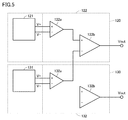
- FIG. 5 is a circuit diagram showing a circuit configuration of the current sensor according to the first embodiment of the present invention.
- the IC chip 122 of the first magnetic sensor 120 differentially amplifies the midpoint potential (V +) and the midpoint potential (V ⁇ ) of the bridge circuit of the plurality of magnetoresistive elements 121.
- a differential amplifier 122a that outputs the calculated voltage value ((V +) ⁇ (V ⁇ )) is included.
- the IC chip 132 of the second magnetic sensor 130 has a voltage value calculated by differentially amplifying the midpoint potential (V +) and the midpoint potential (V ⁇ ) of the bridge circuit of the plurality of magnetoresistive elements 131 (( A differential amplifier 132a that outputs (V +)-(V-)) is included.
- the IC chip 122 of the first magnetic sensor 120 calculates the output voltage of the bridge circuit of the plurality of magnetoresistive elements 121 and the output voltage of the bridge circuit of the bridge circuit of the plurality of magnetoresistive elements 131 by calculating the output voltage.
- a calculation unit that calculates the value of current 1 is further included.
- the IC chip 122 of the first magnetic sensor 120 has a differential amplifier 122b as a calculation unit.
- the differential amplifier 122b is connected to the differential amplifier 122a and the differential amplifier 132a. Note that a subtractor may be used as the calculation unit.
- the IC chip 132 of the second magnetic sensor 130 calculates the output voltage of the bridge circuit of the plurality of magnetoresistive elements 121 and the output voltage of the bridge circuit of the bridge circuit of the plurality of magnetoresistive elements 131 by calculating the output voltage.
- a calculation unit that can calculate the value of current 1 is further included.
- the IC chip 132 of the second magnetic sensor 130 has a differential amplifier 132b as a calculation unit. Note that a subtractor may be used as the calculation unit.
- the differential amplifier 132b is not connected to the differential amplifier 122a and the differential amplifier 132a, but instead of the differential amplifier 122b, the differential amplifier 132b is connected to the differential amplifier 122a and the differential amplifier 132a. Also good.
- the first bias magnet 140 and the second bias magnet 150 are arranged at intervals in the longitudinal direction (X-axis direction).
- the flat portion 113 is located between them, and the center 140c of the first bias magnet 140 and the second bias magnet 150 in the height direction (Z-axis direction). Is located within the range where the flat portion 113 is located in the height direction (Z-axis direction).
- each of the first bias magnet 140 and the second bias magnet 150 has a quadrangular prism shape.
- the first bias magnet 140 is disposed on the first flat portion 116.
- the second bias magnet 150 is disposed on the second flat part 117.
- Each of the first bias magnet 140 and the second bias magnet 150 is fixed to the conductor 110 by die bonding.
- the center 140c and the center 150c are intermediate between the position of the highest portion and the position of the lowest portion of each of the first bias magnet 140 and the second bias magnet 150 in the height direction (Z-axis direction). Position.
- the plurality of magnetoresistive elements 121 of the first magnetic sensor 120 and the plurality of magnetoresistive elements 131 of the second magnetic sensor 130 are located in a region sandwiched between the first bias magnet 140 and the second bias magnet 150. is doing.
- the N pole of the first bias magnet 140 and the S pole of the second bias magnet 150 are opposed to each other in the longitudinal direction (X-axis direction). Note that the S pole of the first bias magnet 140 and the N pole of the second bias magnet 150 may face each other in the longitudinal direction (X-axis direction).
- a bias magnetic field parallel to the longitudinal direction (X-axis direction) is generated between the first bias magnet 140 and the second bias magnet 150. Since the conductor 110 is made of a non-magnetic material, the bias magnetic field generated between the first bias magnet 140 and the second bias magnet 150 causes the first extending portion 114 and the second extending portion 115 to pass through. It is generated parallel to the longitudinal direction (X-axis direction).
- the plurality of magnetoresistive elements 121 of the first magnetic sensor 120 and the plurality of magnetoresistive elements 131 of the second magnetic sensor 130 are respectively interposed between the first bias magnet 140 and the second bias magnet 150.
- the generated bias magnetic field can be applied.
- each of the first bias magnet 140 and the second bias magnet 150 isotropic ferrite, anisotropic ferrite, samarium cobalt, alnico, neodymium, or the like can be used.
- Each of the first bias magnet 140 and the second bias magnet 150 may be composed of a sintered magnet or a bonded magnet.
- the conductor 110, the first magnetic sensor 120, the second magnetic sensor 130, the first bias magnet 140, and the second bias magnet 150 are integrated by the sealing resin 160.
- the sealing resin 160 a silicone resin or an epoxy resin can be used.
- the end of the conductor 110 on one side in the longitudinal direction (X-axis direction) and the end of the conductor 110 on the other side in the longitudinal direction (X-axis direction) are not covered with the sealing resin 160 and are exposed. Yes.
- connection terminals 170 and a plurality of connection terminals 171 are drawn from the sealing resin 160 in the width direction (Y-axis direction) of the conductor 110.
- the Vcc terminal is connected to the Vcc terminals of the bridge circuit of the plurality of magnetoresistive elements 121 of the first magnetic sensor 120 shown in FIG.
- the GND terminal of the plurality of connection terminals 170 is connected to the GND terminal of the bridge circuit of the plurality of magnetoresistive elements 121 of the first magnetic sensor 120 shown in FIG.
- the Vout terminal among the plurality of connection terminals 170 is connected to the Vout terminal of the IC chip 122 shown in FIG.
- the Vcc terminal of the plurality of connection terminals 171 is connected to the Vcc terminal of the bridge circuit of the plurality of magnetoresistive elements 131 of the second magnetic sensor 130 shown in FIG.
- the GND terminal of the plurality of connection terminals 171 is connected to the GND terminal of the bridge circuit of the plurality of magnetoresistive elements 131 of the second magnetic sensor 130 shown in FIG.
- the Vout terminal among the plurality of connection terminals 171 is connected to the Vout terminal of the IC chip 132 shown in FIG.
- the magnetic field 110e is generated when the current 1 to be measured flows through the flat portion 113 of the conductor 110.
- the direction of the magnetic field 110e in the width direction (Y-axis direction) of the conductor 110 is opposite to each other on the one main surface 111 side of the flat portion 113 and the other main surface 112 side of the flat portion 113. Therefore, the direction of the magnetic field 110e acting on the first magnetic sensor 120 and the direction of the magnetic field 110e acting on the second magnetic sensor 130 are opposite to each other.
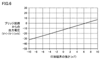
- FIG. 6 shows the relationship between the output voltage ((V +) ⁇ (V ⁇ )) (mV) from each bridge circuit of the first magnetic sensor and the second magnetic sensor and the strength of the applied magnetic field (mT). It is a graph to show.
- the vertical axis represents the output voltage ((V +) ⁇ (V ⁇ )) (mV) from the bridge circuit, and the horizontal axis represents the strength of the applied magnetic field (mT).
- the output voltage from each bridge circuit of the first magnetic sensor 120 and the second magnetic sensor 130 to which a bias magnetic field is applied from the first bias magnet 140 and the second bias magnet 150 is applied. Proportional to the strength of the magnetic field.
- the first magnetic sensor 120 outputs a positive value when detecting a magnetic field directed in one direction of the detection axis 120a shown in FIG. 3, and is directed in a direction opposite to the one direction of the detection axis 120a. It has an odd function input / output characteristic that outputs a negative value when a magnetic field is detected.
- the direction of the detection axis 120a of the first magnetic sensor 120 is parallel to the width direction (Y-axis direction) of the conductor 110.
- the second magnetic sensor 130 outputs a positive value when detecting a magnetic field directed in one direction of the detection axis 130a, and detects a magnetic field directed in a direction opposite to the one direction of the detection axis 130a. In this case, it has an odd function input / output characteristic that outputs a negative value.
- the direction of the detection axis 130a of the second magnetic sensor 130 is parallel to the width direction (Y-axis direction) of the conductor 110.
- FIG. 7 is a schematic diagram showing a state in which a magnetic field generated by a current to be measured flowing through a conductor and an external magnetic field are applied to each of the first magnetic sensor and the second magnetic sensor.
- the directions of the magnetic field components in the directions are opposite to each other.
- the conductor 110 is located between the first magnetic sensor 120 and the second magnetic sensor 130, the external magnetic field source is a physical sensor. Therefore, it cannot be positioned between the first magnetic sensor 120 and the second magnetic sensor 130.
- the direction of the magnetic field component in the direction of the detection axis 120a and the external magnetic field applied to the second magnetic sensor 130 from the external magnetic field source are the same as each other.
- FIG. 8 shows the value of the current to be measured flowing through the conductor and the bridge circuit of each of the first magnetic sensor and the second magnetic sensor when an external magnetic field is applied to the first magnetic sensor and the second magnetic sensor. It is a graph which shows the relationship with an output voltage.
- the vertical axis represents the output voltage of each bridge circuit of the first magnetic sensor 120 and the second magnetic sensor 130
- the horizontal axis represents the value of the current 1 to be measured flowing through the conductor 110.
- the phase of the output voltage ( ⁇ I) of FIG. Therefore, if the output voltage ⁇ I of the bridge circuit of the first magnetic sensor 120 is a positive value, the output voltage ( ⁇ I) of the bridge circuit of the second magnetic sensor 130 is a negative value.
- the phase of the output voltage ⁇ N of the bridge circuit of the first magnetic sensor 120 and the phase of the output voltage ⁇ N of the bridge circuit of the second magnetic sensor 130 are in phase. Therefore, when the output voltage ⁇ N of the bridge circuit of the first magnetic sensor 120 is a positive value, the output voltage ⁇ N of the bridge circuit of the second magnetic sensor 130 is also a positive value.
- the output voltage from the bridge circuit of the first magnetic sensor 120 is ( ⁇ I + ⁇ N)
- the output voltage from the bridge circuit of the second magnetic sensor 130 is ( ⁇ ⁇ I + ⁇ N).
- the output voltage ( ⁇ I + ⁇ N) of the bridge circuit of the first magnetic sensor 120 and the output voltage ( ⁇ I + ⁇ N) of the bridge circuit of the second magnetic sensor 130 are calculated by the differential amplifier 122b shown in FIG. .
- FIG. 9 is a graph showing the relationship between the value of the current to be measured flowing through the conductor and the output voltage of the current sensor according to Embodiment 1 of the present invention.
- the vertical axis represents the output voltage of the current sensor 100
- the horizontal axis represents the value of the current 1 to be measured flowing through the conductor 110.
- the differential amplifier 122b As shown in FIG. 9, in the differential amplifier 122b, the difference between the output voltage ( ⁇ I + ⁇ N) of the bridge circuit of the first magnetic sensor 120 and the output voltage ( ⁇ I + ⁇ N) of the bridge circuit of the second magnetic sensor 130. Is calculated, the output voltage of the current sensor 100 becomes 2 ⁇ I. From this output voltage 2 ⁇ I, the value of the current 1 to be measured flowing through the conductor 110 is calculated. Thus, by calculating the value of the current 1 to be measured flowing through the conductor 110, the influence of the external magnetic field on the measured value of the current sensor 100 can be reduced, and the current 1 to be measured flowing through the conductor 110 can be reduced. Detection sensitivity can be increased.
- the magnetic field 110e generated by the current 1 to be measured flowing through the flat portion 113 of the conductor 110 is strongly and stable. Therefore, the first magnetic sensor 120 is disposed on one main surface 111 of the flat portion 113, and the second magnetic sensor 130 is disposed on the other main surface 112 of the flat portion 113. The stability of the measured value of the current sensor 100 can be ensured while increasing the detection sensitivity of the current 1 to be measured flowing through the conductor 110.
- the first magnetic sensor 120 disposed on the one main surface 111 side of the conductor 110 and the other main surface 112 side of the conductor 110 are disposed by a pair of bias magnets. Since a bias magnetic field can be applied to both of the second magnetic sensors 130, the current sensor 100 can be reduced in size.
- a plurality of magnetoresistive elements 121 are formed on the IC chip 122, and in the second magnetic sensor 130, a plurality of magnetoresistive elements 131 are formed on the IC chip 132, so that a current sensor is formed. 100 can be integrated with high density.
- the current sensor 100 can be easily handled. It is.
- the current sensor 200 according to the second embodiment of the present invention is mainly the current sensor according to the first embodiment in terms of the phase of the output voltage of the bridge circuit of the first magnetic sensor 120 and the second magnetic sensor 130 and the configuration of the calculation unit. Since it is different from the configuration of 100, the description of the same configuration as the current sensor 100 according to the first embodiment will not be repeated.
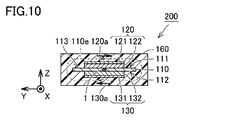
- FIG. 10 is a cross-sectional view showing the configuration of the current sensor according to Embodiment 2 of the present invention.
- FIG. 11 is a circuit diagram showing a circuit configuration of a current sensor according to Embodiment 2 of the present invention.
- FIG. 10 shows the same cross-sectional view as FIG.
- the first magnetic sensor 120 outputs a positive value when detecting a magnetic field directed in one direction of the detection axis 120a, and is directed in a direction opposite to the one direction of the detection axis 120a. It has an odd function input / output characteristic that outputs a negative value when a detected magnetic field is detected.
- the direction of the detection axis 120a of the first magnetic sensor 120 is parallel to the width direction (Y-axis direction) of the conductor 110.
- the second magnetic sensor 130 outputs a negative value when detecting a magnetic field directed in one direction of the detection axis 130a, and detects a magnetic field directed in a direction opposite to the one direction of the detection axis 130a. It has an odd function input / output characteristic that outputs a positive value.
- the direction of the detection axis 130a of the second magnetic sensor 130 is parallel to the width direction (Y-axis direction) of the conductor 110.
- the magnetization direction of the magnetoresistive film included in each of the plurality of magnetoresistive elements 121 and the plurality of magnetoresistive elements 131 is the application direction of the bias magnetic field applied from the first bias magnet 140 and the second bias magnet 150, and It is determined by the shape anisotropy of the magnetoresistive film. For example, when the aspect ratio of the planar shape of the magnetoresistive film is small, the influence of the shape anisotropy of the magnetoresistive film is small, and the application direction of the bias magnetic field applied from the first bias magnet 140 and the second bias magnet 150 is the main cause. Thus, the magnetization direction of the magnetoresistive film is determined. On the other hand, when the shape anisotropy of the magnetoresistive film is large, the influence of the shape anisotropy of the magnetoresistive film on the magnetization direction of the magnetoresistive film becomes large.
- the first magnetic sensor 120 and the second bias magnet 150 can be changed from the first magnetic sensor 120 and the second magnetic bias magnet 150 by changing the aspect ratios of the planar shapes of the magnetoresistive films of the plurality of magnetoresistive elements 121 and 131. Even if the application direction of the bias magnetic field applied to the second magnetic sensor 130 is the same, only the phases of the output voltages of the first magnetic sensor 120 and the second magnetic sensor 130 with respect to the magnetic field applied in the same direction are different from each other. be able to.
- the IC chip 122 of the first magnetic sensor 120 has the output voltage of the bridge circuit of the plurality of magnetoresistive elements 121 and the output voltage of the bridge circuit of the bridge circuit of the plurality of magnetoresistive elements 131, It has a calculation part which calculates the value of current 1 to be measured by calculation.
- the IC chip 122 of the first magnetic sensor 120 has a summing amplifier 222b as a calculation unit.
- the summing amplifier 222b is connected to the differential amplifier 122a and the differential amplifier 132a.
- An adder may be used as the calculation unit.
- the IC chip 132 of the second magnetic sensor 130 calculates the output voltage of the bridge circuit of the plurality of magnetoresistive elements 121 and the output voltage of the bridge circuit of the bridge circuit of the plurality of magnetoresistive elements 131 by calculating the output voltage.
- a calculation unit that can calculate the value of current 1 is further included.
- the IC chip 132 of the second magnetic sensor 130 has a summing amplifier 232b as a calculation unit. An adder may be used as the calculation unit.
- the summing amplifier 232b is not connected to the differential amplifier 122a and the differential amplifier 132a, the summing amplifier 232b may be connected to the differential amplifier 122a and the differential amplifier 132a instead of the summing amplifier 222b.
- the phase of the output voltage ⁇ I of the bridge circuit of the first magnetic sensor 120 and the bridge circuit of the second magnetic sensor 130 are in phase. Therefore, when the output voltage ⁇ I of the bridge circuit of the first magnetic sensor 120 is a positive value, the output voltage ⁇ I of the bridge circuit of the second magnetic sensor 130 is also a positive value.
- the phase of the output voltage ⁇ N of the bridge circuit of the first magnetic sensor 120 is opposite to the phase of the output voltage ( ⁇ N) of the bridge circuit of the second magnetic sensor 130. . Therefore, if the output voltage ⁇ N of the bridge circuit of the first magnetic sensor 120 is a positive value, the output voltage ( ⁇ N) of the bridge circuit of the second magnetic sensor 130 is a negative value.
- the output voltage from the bridge circuit of the first magnetic sensor 120 is ( ⁇ I + ⁇ N)
- the output voltage from the bridge circuit of the second magnetic sensor 130 is ( ⁇ I + ( ⁇ ⁇ N)).
- the output voltage ( ⁇ I + ⁇ N) of the bridge circuit of the first magnetic sensor 120 and the output voltage ( ⁇ I + ( ⁇ ⁇ N)) of the bridge circuit of the second magnetic sensor 130 are calculated by the addition amplifier 222b shown in FIG.
- the addition amplifier 222b shown in FIG.
- the output voltage ( ⁇ I + ⁇ N) of the bridge circuit of the first magnetic sensor 120 and the output voltage ( ⁇ I + ( ⁇ ⁇ N)) of the bridge circuit of the second magnetic sensor 130 are added, thereby obtaining a current.
- the output voltage of the sensor 200 is 2 ⁇ I. From this output voltage 2 ⁇ I, the value of the current 1 to be measured flowing through the conductor 110 is calculated.
- the influence of the external magnetic field on the measured value of the current sensor 200 can be reduced, and the current 1 to be measured flowing through the conductor 110 can be reduced. Detection sensitivity can be increased.
Landscapes
- Physics & Mathematics (AREA)
- General Physics & Mathematics (AREA)
- Measuring Instrument Details And Bridges, And Automatic Balancing Devices (AREA)
- Measuring Magnetic Variables (AREA)
Abstract
1対のバイアス磁石(140,150)は、第1磁気センサ(120)および第2磁気センサ(130)にバイアス磁界を印加する。導体(110)は、長手方向に延在する平坦部(113)、および、平坦部(113)の長手方向の両端から他方の主面(112)側に曲がって延在する1対の延在部(114,115)を有する。第1磁気センサ(120)および第2磁気センサ(130)の各々は、平坦部(113)に沿って位置している。1対のバイアス磁石(140,150)においては、互いの間に平坦部(113)が位置し、かつ、平坦部(113)の一方の主面(111)に直交する高さ方向における1対のバイアス磁石(140,150)の各々の中心(140c,150c)が、高さ方向において平坦部(113)が位置している範囲内に位置している。
Description
本発明は、電流センサに関する。
電流検出装置の構成を開示した先行文献として、特開2014-55839号公報(特許文献1)がある。特許文献1に記載された電流検出装置は、電流が流れる導線と、導線の少なくとも一部が貫通する状態で挿入される挿入部が形成された基板と、基板に搭載され、導線を流れる電流により導線のまわりに発生する磁束を検出する1対の磁気検出素子とを備える。
磁気センサの構成を開示した先行文献として、特開平6-148301号公報(特許文献2)がある。特許文献2に記載された磁気センサは、硬質磁性膜よりなるバイアス磁界発生部と強磁性薄膜よりなる磁気抵抗素子とが、同一チップ上に形成されて成る。バイアス磁界発生部においては、2個の薄膜磁石が、各々の異極が対向するように、互いに間隔をあけて配置されている。磁気抵抗素子は、2個の薄膜磁石の作る磁界の中心付近に配置されている。
磁気抵抗素子にバイアス磁界を印加するバイアス磁石が、磁気センサ毎に設けられている場合、電流センサを小型化することができない。
本発明は上記の問題点に鑑みてなされたものであって、小型化された電流センサを提供することを目的とする。
本発明に基づく電流センサは、導体と、第1磁気センサと、第2磁気センサと、1対のバイアス磁石とを備える。導体は、長手方向、一方の主面、および、上記一方の主面とは反対側に位置する他方の主面を有する。導体は、非磁性体からなる。導体には、測定対象の電流が流れる。第1磁気センサは、上記一方の主面上に配置されている。第1磁気センサは、導体を流れる上記測定対象の電流により発生する磁界の強さを検出する。第2磁気センサは、導体を間に挟んで第1磁気センサと対向するように上記他方の主面上に配置されている。第2磁気センサ、導体を流れる上記測定対象の電流により発生する磁界の強さを検出する。1対のバイアス磁石は、上記長手方向において互いに間隔をあけて配置されている。1対のバイアス磁石は、第1磁気センサおよび第2磁気センサにバイアス磁界を印加する。導体は、上記長手方向に延在する平坦部、および、平坦部の上記長手方向の両端から他方の主面側に曲がって延在する1対の延在部を有する。第1磁気センサおよび第2磁気センサの各々は、平坦部に沿って位置している。1対のバイアス磁石においては、互いの間に平坦部が位置し、かつ、平坦部の上記一方の主面に直交する高さ方向における1対のバイアス磁石の各々の中心が、上記高さ方向において平坦部が位置している範囲内に位置している。
本発明の一形態においては、上記高さ方向における1対のバイアス磁石の各々の中心を結ぶ仮想線上に、上記高さ方向における平坦部の中心が位置している。
本発明の一形態においては、第1磁気センサおよび第2磁気センサの各々は、ブリッジ回路を構成する複数の磁気抵抗素子、および、第1磁気センサのブリッジ回路の出力電圧と第2磁気センサのブリッジ回路の出力電圧とを演算することにより、上記測定対象の電流の値を算出する算出部を有するIC(Integrated Circuit)チップを含む。複数の磁気抵抗素子は、ICチップ上に形成されている。
本発明の一形態においては、第1磁気センサおよび第2磁気センサの各々において、ICチップが平坦部と対向している。
本発明の一形態においては、導体を流れる上記測定対象の電流により発生する磁界に対して、第1磁気センサのブリッジ回路の出力電圧の位相と、第2磁気センサのブリッジ回路の出力電圧の位相とが、逆相である。算出部が、減算器または差動増幅器である。
本発明の一形態においては、導体を流れる上記測定対象の電流により発生する磁界に対して、第1磁気センサのブリッジ回路の出力電圧の位相と、第2磁気センサのブリッジ回路の出力電圧の位相とが、同相である。算出部が、加算器または加算増幅器である。
本発明の一形態においては、導体、第1磁気センサ、第2磁気センサ、および、1対のバイアス磁石が、封止樹脂によって一体となっている。
本発明によれば、電流センサを小型化することができる。
以下、本発明の各実施形態に係る電流センサについて図を参照して説明する。以下の実施形態の説明においては、図中の同一または相当部分には同一符号を付して、その説明は繰り返さない。
(実施形態1)
図1は、本発明の実施形態1に係る電流センサの構成を示す側面図である。図2は、図1の電流センサを矢印II方向から見た平面図である。図3は、図2の電流センサをIII-III線矢印方向から見た断面図である。図1~3においては、後述する導体110の長手方向をX軸方向、導体110の幅方向をY軸方向、高さ方向をZ軸方向として、図示している。
図1は、本発明の実施形態1に係る電流センサの構成を示す側面図である。図2は、図1の電流センサを矢印II方向から見た平面図である。図3は、図2の電流センサをIII-III線矢印方向から見た断面図である。図1~3においては、後述する導体110の長手方向をX軸方向、導体110の幅方向をY軸方向、高さ方向をZ軸方向として、図示している。
図1~3に示すように、本発明の実施形態1に係る電流センサ100は、導体110と、第1磁気センサ120と、第2磁気センサ130と、1対のバイアス磁石とを備える。1対のバイアス磁石は、第1バイアス磁石140と第2バイアス磁石150とからなる。
導体110は、長手方向(X軸方向)、一方の主面111、および、一方の主面111とは反対側に位置する他方の主面112を有する。導体110は、長手方向(X軸方向)に延在する平坦部113、および、平坦部113の長手方向(X軸方向)の両端から他方の主面112側に曲がって延在する1対の延在部を有する。
平坦部113の一方の主面111に直交する方向が、高さ方向(Z軸方向)である。導体110の長手方向(X軸方向)および高さ方向(Z軸方向)の各々に直交する方向が、導体110の幅方向(Y軸方向)である。本実施形態においては、導体110の幅は、略一定である。
1対の延在部は、平坦部113の長手方向(X軸方向)の一端から他方の主面112側に曲がって延在する第1延在部114と、平坦部113の長手方向(X軸方向)の他端から他方の主面112側に曲がって延在する第2延在部115とからなる。本実施形態においては、第1延在部114および第2延在部115の各々は、高さ方向(Z軸方向)に沿って延在している。高さ方向(Z軸方向)における、第1延在部114の長さと、第2延在部115の長さとは、略同一である。
導体110は、第1延在部114の一端から長手方向(X軸方向)の一方側に向かって延在する第1平坦部116、および、第2延在部115の一端から長手方向(X軸方向)の他方側に向かって延在する第2平坦部117をさらに有する。本実施形態においては、第1平坦部116および第2平坦部117の各々の延在方向は、平坦部113の延在方向と平行である。なお、導体110は、必ずしも第1平坦部116および第2平坦部117を有していなくてもよく、少なくとも平坦部113および1対の延在部を有していればよい。
導体110には、測定対象の電流1が流れる。本実施形態においては、長手方向(X軸方向)の一方側の導体110の端部から、長手方向(X軸方向)の他方側の導体110の端部に向かって、測定対象の電流1が流れる。
導体110は、非磁性体からなる。本実施形態においては、導体110は、銅で構成されている。ただし、導体110の材料は、銅に限られず、金、銀、アルミニウムなどの非磁性体でもよい。
本実施形態においては、薄板をプレス加工することにより導体110を形成している。ただし、導体110の形成方法は、これに限られず、切削または鋳造などでもよい。
第1磁気センサ120は、導体110を流れる測定対象の電流1により発生する磁界の強さを検出する。第1磁気センサ120は、導体110の一方の主面111上に配置されている。第1磁気センサ120は、平坦部113に沿って位置している。本実施形態においては、第1磁気センサ120は、図示しない絶縁膜を間に挟んで平坦部113の一方の主面111と接している。本実施形態においては、第1磁気センサ120は、ダイボンディングにより導体110に対して固定されている。
図3に示すように、第1磁気センサ120は、複数の磁気抵抗素子121およびICチップ122を含む。複数の磁気抵抗素子121は、ICチップ122上に形成されている。複数の磁気抵抗素子121は、パーマロイなどの強磁性体からなるパターニングされた磁気抵抗膜を含む。ICチップ122は、平坦部113と対向している。
第2磁気センサ130は、導体110を流れる測定対象の電流1により発生する磁界の強さを検出する。第2磁気センサ130は、導体110を間に挟んで第1磁気センサ120と対向するように、導体110の他方の主面112上に配置されている。第2磁気センサ130は、平坦部113に沿って位置している。本実施形態においては、第2磁気センサ130は、図示しない絶縁膜を間に挟んで平坦部113の他方の主面112と接している。第2磁気センサ130は、ダイボンディングにより導体110に対して固定されている。
図3に示すように、第2磁気センサ130は、複数の磁気抵抗素子131およびICチップ132を含む。複数の磁気抵抗素子131は、ICチップ132上に形成されている。複数の磁気抵抗素子131は、パーマロイなどの強磁性体からなるパターニングされた磁気抵抗膜を含む。ICチップ132は、平坦部113と対向している。
図4は、第1磁気センサおよび第2磁気センサの各々の複数の磁気抵抗素子が構成するブリッジ回路を示す回路図である。本実施形態においては、図4に示すように、第1磁気センサ120の複数の磁気抵抗素子121、および、第2磁気センサ130の複数の磁気抵抗素子131、の各々は、ホイートストンブリッジ型のブリッジ回路を構成する4つのAMR(Anisotropic Magneto Resistance)素子MR1~MR4からなる。なお、ホイートストンブリッジ型のブリッジ回路は、図4に示すフルブリッジ回路に限られず、ハーフブリッジ回路でもよい。
図5は、本発明の実施形態1に係る電流センサの回路構成を示す回路図である。図5に示すように、第1磁気センサ120のICチップ122は、複数の磁気抵抗素子121のブリッジ回路の中点電位(V+)と中点電位(V-)とを差動増幅して算出された電圧値((V+)-(V-))を出力する差動増幅器122aを有する。第2磁気センサ130のICチップ132は、複数の磁気抵抗素子131のブリッジ回路の中点電位(V+)と中点電位(V-)とを差動増幅して算出された電圧値((V+)-(V-))を出力する差動増幅器132aを有する。
第1磁気センサ120のICチップ122は、複数の磁気抵抗素子121のブリッジ回路の出力電圧と、複数の磁気抵抗素子131のブリッジ回路のブリッジ回路の出力電圧とを、演算することにより測定対象の電流1の値を算出する算出部をさらに有する。本実施形態においては、第1磁気センサ120のICチップ122は、算出部として差動増幅器122bを有している。差動増幅器122bは、差動増幅器122aおよび差動増幅器132aと接続されている。なお、算出部として、減算器が用いられていてもよい。
第2磁気センサ130のICチップ132は、複数の磁気抵抗素子121のブリッジ回路の出力電圧と、複数の磁気抵抗素子131のブリッジ回路のブリッジ回路の出力電圧とを、演算することにより測定対象の電流1の値を算出可能な算出部をさらに有する。本実施形態においては、第2磁気センサ130のICチップ132は、算出部として差動増幅器132bを有している。なお、算出部として、減算器が用いられていてもよい。差動増幅器132bは、差動増幅器122aおよび差動増幅器132aとは接続されていないが、差動増幅器122bの代わりに、差動増幅器132bが差動増幅器122aおよび差動増幅器132aと接続されていてもよい。
図1,2に示すように、第1バイアス磁石140と第2バイアス磁石150とは、長手方向(X軸方向)において互いに間隔をあけて配置されている。第1バイアス磁石140および第2バイアス磁石150においては、互いの間に平坦部113が位置し、かつ、高さ方向(Z軸方向)における第1バイアス磁石140の中心140cおよび第2バイアス磁石150の中心150cが、高さ方向(Z軸方向)において平坦部113が位置している範囲内に位置している。
具体的には、第1バイアス磁石140および第2バイアス磁石150の各々は、四角柱状の形状を有している。第1バイアス磁石140は、第1平坦部116上に配置されている。第2バイアス磁石150は、第2平坦部117上に配置されている。第1バイアス磁石140および第2バイアス磁石150の各々は、ダイボンディングにより導体110に対して固定されている。
本実施形態においては、高さ方向(Z軸方向)における第1バイアス磁石140の中心140cと第2バイアス磁石150の中心150cとを結ぶ仮想線L上に、高さ方向(Z軸方向)における平坦部113の中心が位置している。ここで、中心140cおよび中心150cとは、第1バイアス磁石140および第2バイアス磁石150の、各々の高さ方向(Z軸方向)における最も高い部分の位置と最も低い部分の位置との中間の位置である。
第1磁気センサ120の複数の磁気抵抗素子121、および、第2磁気センサ130の複数の磁気抵抗素子131は、第1バイアス磁石140と第2バイアス磁石150との間に挟まれた領域に位置している。
第1バイアス磁石140のN極と第2バイアス磁石150のS極とが、長手方向(X軸方向)にて互いに対向している。なお、第1バイアス磁石140のS極と第2バイアス磁石150のN極とが、長手方向(X軸方向)にて互いに対向していてもよい。
第1バイアス磁石140と第2バイアス磁石150との間に、長手方向(X軸方向)に平行なバイアス磁界が発生する。なお、導体110が非磁性体で構成されているため、第1バイアス磁石140と第2バイアス磁石150との間に発生したバイアス磁界は、第1延在部114および第2延在部115を貫通して長手方向(X軸方向)に平行に発生する。
その結果、第1磁気センサ120の複数の磁気抵抗素子121、および、第2磁気センサ130の複数の磁気抵抗素子131、の各々に、第1バイアス磁石140と第2バイアス磁石150との間に発生したバイアス磁界を印加することができる。
第1バイアス磁石140および第2バイアス磁石150の各々の材料として、等方性フェライト、異方性フェライト、サマリウムコバルト、アルニコまたはネオジムなどを用いることができる。第1バイアス磁石140および第2バイアス磁石150の各々は、焼結磁石またはボンド磁石で構成されていてもよい。
本実施形態においては、導体110、第1磁気センサ120、第2磁気センサ130、第1バイアス磁石140および第2バイアス磁石150が、封止樹脂160によって一体となっている。封止樹脂160としては、シリコーン樹脂またはエポキシ樹脂を用いることができる。
長手方向(X軸方向)の一方側の導体110の端部、および、長手方向(X軸方向)の他方側の導体110の端部は、封止樹脂160に覆われておらず露出している。
図1,2に示すように、封止樹脂160から、複数の接続端子170および複数の接続端子171が、導体110の幅方向(Y軸方向)に引き出されている。
複数の接続端子170のうちのVcc端子は、図4に示す第1磁気センサ120の複数の磁気抵抗素子121のブリッジ回路のVcc端子と、ボンディングワイヤ180によって接続されている。複数の接続端子170のうちのGND端子は、図4に示す第1磁気センサ120の複数の磁気抵抗素子121のブリッジ回路のGND端子と、ボンディングワイヤ180によって接続されている。複数の接続端子170のうちのVout端子は、図5に示すICチップ122のVout端子と、ボンディングワイヤ180によって接続されている。
複数の接続端子171のうちのVcc端子は、図4に示す第2磁気センサ130の複数の磁気抵抗素子131のブリッジ回路のVcc端子と、ボンディングワイヤ181によって接続されている。複数の接続端子171のうちのGND端子は、図4に示す第2磁気センサ130の複数の磁気抵抗素子131のブリッジ回路のGND端子と、ボンディングワイヤ181によって接続されている。複数の接続端子171のうちのVout端子は、図5に示すICチップ132のVout端子と、ボンディングワイヤ181によって接続されている。
図3に示すように、導体110の平坦部113を測定対象の電流1が流れることにより、磁界110eが発生する。導体110の幅方向(Y軸方向)における磁界110eの向きは、平坦部113の一方の主面111側と、平坦部113の他方の主面112側とでは、互いに反対方向となる。よって、第1磁気センサ120に作用する磁界110eの向きと、第2磁気センサ130に作用する磁界110eの向きとは、互いに反対である。
図6は、第1磁気センサおよび第2磁気センサの各々のブリッジ回路からの出力電圧((V+)-(V-))(mV)と、印加磁界の強さ(mT)との関係を示すグラフである。図6においては、縦軸にブリッジ回路からの出力電圧((V+)-(V-))(mV)、横軸に印加磁界の強さ(mT)を示している。
図6に示すように、第1バイアス磁石140および第2バイアス磁石150からバイアス磁界を印加されている、第1磁気センサ120および第2磁気センサ130の各々のブリッジ回路からの出力電圧は、印加磁界の強さに比例する。
よって、第1磁気センサ120は、図3に示す検出軸120aの一方向に向いた磁界を検出した場合に正の値で出力し、かつ、検出軸120aの一方向とは反対方向に向いた磁界を検出した場合に負の値で出力する、奇関数入出力特性を有している。第1磁気センサ120の検出軸120aの方向は、導体110の幅方向(Y軸方向)と平行である。
同様に、第2磁気センサ130は、検出軸130aの一方向に向いた磁界を検出した場合に正の値で出力し、かつ、検出軸130aの一方向とは反対方向に向いた磁界を検出した場合に負の値で出力する、奇関数入出力特性を有している。第2磁気センサ130の検出軸130aの方向は、導体110の幅方向(Y軸方向)と平行である。
図7は、第1磁気センサおよび第2磁気センサの各々に、導体を流れる測定対象の電流により発生する磁界および外部磁界が印加された状態を示す模式図である。
図3,7に示すように、第1磁気センサ120に作用する磁界110eのうちの検出軸120aの方向における磁界成分の向きと、第2磁気センサ130に作用する磁界110eのうちの検出軸130aの方向における磁界成分の向きとは、互いに反対向きとなる。
図1~3に示すように、本実施形態に係る電流センサ100においては、第1磁気センサ120と第2磁気センサ130との間に導体110が位置しているため、外部磁界源は、物理的に第1磁気センサ120と第2磁気センサ130との間に位置することができない。
そのため、外部磁界源から第1磁気センサ120に印加される外部磁界のうちの検出軸120aの方向における磁界成分の向きと、外部磁界源から第2磁気センサ130に印加される外部磁界のうちの検出軸130aの方向における磁界成分の向きとは、互いに同じ向きとなる。
図8は、外部磁界が第1磁気センサおよび第2磁気センサに印加されている状態において、導体を流れる測定対象の電流の値と、第1磁気センサおよび第2磁気センサの各々のブリッジ回路の出力電圧と、の関係を示すグラフである。図8においては、縦軸に第1磁気センサ120および第2磁気センサ130の各々のブリッジ回路の出力電圧、横軸に導体110を流れる測定対象の電流1の値を示している。
図8に示すように、導体110を流れる測定対象の電流1により発生する磁界110eの強さについて、第1磁気センサ120のブリッジ回路の出力電圧ΔIの位相と、第2磁気センサ130のブリッジ回路の出力電圧(-ΔI)の位相とは、逆相である。よって、第1磁気センサ120のブリッジ回路の出力電圧ΔIを正の値とすると、第2磁気センサ130のブリッジ回路の出力電圧(-ΔI)は負の値となる。
一方、外部磁界10eの強さについて、第1磁気センサ120のブリッジ回路の出力電圧ΔNの位相と、第2磁気センサ130のブリッジ回路の出力電圧ΔNの位相とは、同相である。よって、第1磁気センサ120のブリッジ回路の出力電圧ΔNを正の値とすると、第2磁気センサ130のブリッジ回路の出力電圧ΔNも正の値となる。
その結果、磁界110eおよび外部磁界10eを印加された場合、第1磁気センサ120のブリッジ回路からの出力電圧は(ΔI+ΔN)となり、第2磁気センサ130のブリッジ回路からの出力電圧は(-ΔI+ΔN)となる。
第1磁気センサ120のブリッジ回路の出力電圧(ΔI+ΔN)と第2磁気センサ130のブリッジ回路の出力電圧(-ΔI+ΔN)とは、図5に示す差動増幅器122bにて演算される。
図9は、導体を流れる測定対象の電流の値と、本発明の実施形態1に係る電流センサの出力電圧との関係を示すグラフである。図9においては、縦軸に電流センサ100の出力電圧、横軸に導体110を流れる測定対象の電流1の値を示している。
図9に示すように、差動増幅器122bにおいて、第1磁気センサ120のブリッジ回路の出力電圧(ΔI+ΔN)と第2磁気センサ130のブリッジ回路の出力電圧(-ΔI+ΔN)との差分が算出されることにより、電流センサ100の出力電圧は2ΔIとなる。この出力電圧2ΔIから、導体110を流れる測定対象の電流1の値が算出される。このように、導体110を流れる測定対象の電流1の値を算出することにより、電流センサ100の測定値に対する外部磁界の影響を低減することができるとともに、導体110を流れる測定対象の電流1の検出感度を高くすることができる。
平坦部113の一方の主面111上および他方の主面112上においては、導体110の平坦部113を測定対象の電流1が流れることにより発生する磁界110eが強く安定している。そのため、第1磁気センサ120が平坦部113の一方の主面111上に配置され、第2磁気センサ130が平坦部113の他方の主面112上に配置されていることにより、電流センサ100の導体110を流れる測定対象の電流1の検出感度を高くしつつ、電流センサ100の測定値の安定性を確保することができる。
本実施形態に係る電流センサ100においては、1対のバイアス磁石によって、導体110の一方の主面111側に配置された第1磁気センサ120および導体110の他方の主面112側に配置された第2磁気センサ130の両方にバイアス磁界を印加することができるため、電流センサ100を小型化することができる。
また、第1磁気センサ120において複数の磁気抵抗素子121がICチップ122上に形成され、第2磁気センサ130において複数の磁気抵抗素子131がICチップ132上に形成されていることにより、電流センサ100を高密度に集積化することができる。
さらに、導体110、第1磁気センサ120、第2磁気センサ130、第1バイアス磁石140および第2バイアス磁石150が、封止樹脂160によって一体となっていることにより、電流センサ100の取り扱いが容易である。
(実施形態2)
以下、本発明の実施形態2に係る電流センサについて、図を参照して説明する。本発明の実施形態2に係る電流センサ200は、第1磁気センサ120および第2磁気センサ130のブリッジ回路の出力電圧の位相、および、算出部の構成が、主に実施形態1に係る電流センサ100の構成と異なるため、実施形態1に係る電流センサ100と同様の構成については、説明を繰り返さない。
以下、本発明の実施形態2に係る電流センサについて、図を参照して説明する。本発明の実施形態2に係る電流センサ200は、第1磁気センサ120および第2磁気センサ130のブリッジ回路の出力電圧の位相、および、算出部の構成が、主に実施形態1に係る電流センサ100の構成と異なるため、実施形態1に係る電流センサ100と同様の構成については、説明を繰り返さない。
図10は、本発明の実施形態2に係る電流センサの構成を示す断面図である。図11は、本発明の実施形態2に係る電流センサの回路構成を示す回路図である。図10においては、図3と同一の断面視にて示している。
図10に示すように、第1磁気センサ120は、検出軸120aの一方向に向いた磁界を検出した場合に正の値で出力し、かつ、検出軸120aの一方向とは反対方向に向いた磁界を検出した場合に負の値で出力する、奇関数入出力特性を有している。第1磁気センサ120の検出軸120aの方向は、導体110の幅方向(Y軸方向)と平行である。
第2磁気センサ130は、検出軸130aの一方向に向いた磁界を検出した場合に負の値で出力し、かつ、検出軸130aの一方向とは反対方向に向いた磁界を検出した場合に正の値で出力する、奇関数入出力特性を有している。第2磁気センサ130の検出軸130aの方向は、導体110の幅方向(Y軸方向)と平行である。
複数の磁気抵抗素子121および複数の磁気抵抗素子131の各々に含まれる磁気抵抗膜の磁化方向は、第1バイアス磁石140と第2バイアス磁石150とからから印加されるバイアス磁界の印加方向、および、磁気抵抗膜の形状異方性によって決まる。たとえば、磁気抵抗膜の平面形状のアスペクト比が小さい場合、磁気抵抗膜の形状異方性の影響が小さく、第1バイアス磁石140と第2バイアス磁石150から印加されるバイアス磁界の印加方向が主因となって磁気抵抗膜の磁化方向が決まる。一方、磁気抵抗膜の形状異方性が大きい場合は、磁気抵抗膜の磁化方向に対する、磁気抵抗膜の形状異方性の影響が大きくなる。
よって、複数の磁気抵抗素子121および複数の磁気抵抗素子131の磁気抵抗膜の平面形状のアスペクト比を異ならせることにより、第1バイアス磁石140と第2バイアス磁石150とから第1磁気センサ120および第2磁気センサ130に印加されるバイアス磁界の印加方向が同一であっても、同一方向に印加される磁界に対する第1磁気センサ120および第2磁気センサ130の出力電圧の位相のみを互いに異ならせることができる。
図11に示すように、第1磁気センサ120のICチップ122は、複数の磁気抵抗素子121のブリッジ回路の出力電圧と、複数の磁気抵抗素子131のブリッジ回路のブリッジ回路の出力電圧とを、演算することにより測定対象の電流1の値を算出する算出部を有する。本実施形態においては、第1磁気センサ120のICチップ122は、算出部として加算増幅器222bを有している。加算増幅器222bは、差動増幅器122aおよび差動増幅器132aと接続されている。なお、算出部として、加算器が用いられていてもよい。
第2磁気センサ130のICチップ132は、複数の磁気抵抗素子121のブリッジ回路の出力電圧と、複数の磁気抵抗素子131のブリッジ回路のブリッジ回路の出力電圧とを、演算することにより測定対象の電流1の値を算出可能な算出部をさらに有する。本実施形態においては、第2磁気センサ130のICチップ132は、算出部として加算増幅器232bを有している。なお、算出部として、加算器が用いられていてもよい。加算増幅器232bは、差動増幅器122aおよび差動増幅器132aとは接続されていないが、加算増幅器222bの代わりに、加算増幅器232bが差動増幅器122aおよび差動増幅器132aと接続されていてもよい。
本実施形態においては、導体110を流れる測定対象の電流1により発生する磁界110eの強さについて、第1磁気センサ120のブリッジ回路の出力電圧ΔIの位相と、第2磁気センサ130のブリッジ回路の出力電圧ΔIの位相とは、同相である。よって、第1磁気センサ120のブリッジ回路の出力電圧ΔIを正の値とすると、第2磁気センサ130のブリッジ回路の出力電圧ΔIも正の値となる。
一方、外部磁界10eの強さについて、第1磁気センサ120のブリッジ回路の出力電圧ΔNの位相と、第2磁気センサ130のブリッジ回路の出力電圧(-ΔN)の位相とは、逆相である。よって、第1磁気センサ120のブリッジ回路の出力電圧ΔNを正の値とすると、第2磁気センサ130のブリッジ回路の出力電圧(-ΔN)は負の値となる。
その結果、磁界110eおよび外部磁界10eを印加された場合、第1磁気センサ120のブリッジ回路からの出力電圧は(ΔI+ΔN)となり、第2磁気センサ130のブリッジ回路からの出力電圧は(ΔI+(-ΔN))となる。
第1磁気センサ120のブリッジ回路の出力電圧(ΔI+ΔN)と第2磁気センサ130のブリッジ回路の出力電圧(ΔI+(-ΔN))とは、図11に示す加算増幅器222bにて演算される。
加算増幅器222bにおいて、第1磁気センサ120のブリッジ回路の出力電圧(ΔI+ΔN)と第2磁気センサ130のブリッジ回路の出力電圧(ΔI+(-ΔN))とが加算されることにより、電流センサ200の出力電圧は2ΔIとなる。この出力電圧2ΔIから、導体110を流れる測定対象の電流1の値が算出される。このように、導体110を流れる測定対象の電流1の値を算出することにより、電流センサ200の測定値に対する外部磁界の影響を低減することができるとともに、導体110を流れる測定対象の電流1の検出感度を高くすることができる。
上述した実施形態の説明において、組み合わせ可能な構成を相互に組み合わせてもよい。
今回開示された実施形態はすべての点で例示であって制限的なものではないと考えられるべきである。本発明の範囲は上記した説明ではなくて請求の範囲によって示され、請求の範囲と均等の意味および範囲内でのすべての変更が含まれることが意図される。
1 測定対象の電流、2 出力電圧、10e 外部磁界、100,200 電流センサ、110 導体、110e 磁界、111 一方の主面、112 他方の主面、113 平坦部、114 第1延在部、115 第2延在部、116 第1平坦部、117 第2平坦部、120 第1磁気センサ、120a,130a 検出軸、130 第2磁気センサ、121,131 磁気抵抗素子、122,132 チップ、122a,122b,132a,132b 差動増幅器、140 第1バイアス磁石、140c,150c 中心、150 第2バイアス磁石、160 封止樹脂、170,171 接続端子、180,181 ボンディングワイヤ、222b,232b 加算増幅器、MR1~MR4 磁気抵抗素子。
Claims (7)
- 長手方向、一方の主面、および、該一方の主面とは反対側に位置する他方の主面を有し、非磁性体からなり、測定対象の電流を流すための導体と、
前記一方の主面上に配置され、前記導体を流れる前記測定対象の電流により発生する磁界の強さを検出するための第1磁気センサと、
前記導体を間に挟んで前記第1磁気センサと対向するように前記他方の主面上に配置され、前記導体を流れる前記測定対象の電流により発生する磁界の強さを検出するための第2磁気センサと、
前記長手方向において互いに間隔をあけて配置され、前記第1磁気センサおよび前記第2磁気センサにバイアス磁界を印加するための1対のバイアス磁石とを備え、
前記導体は、前記長手方向に延在する平坦部、および、該平坦部の前記長手方向の両端から他方の主面側に曲がって延在する1対の延在部を有し、
前記第1磁気センサおよび前記第2磁気センサの各々は、前記平坦部に沿って位置し、
前記1対のバイアス磁石においては、互いの間に前記平坦部が位置し、かつ、前記平坦部の前記一方の主面に直交する高さ方向における前記1対のバイアス磁石の各々の中心が、前記高さ方向において前記平坦部が位置している範囲内に位置している、電流センサ。 - 前記高さ方向における前記1対のバイアス磁石の各々の中心を結ぶ仮想線上に、前記高さ方向における前記平坦部の中心が位置している、請求項1に記載の電流センサ。
- 前記第1磁気センサおよび前記第2磁気センサの各々は、ブリッジ回路を構成する複数の磁気抵抗素子、および、前記第1磁気センサの前記ブリッジ回路の出力電圧と前記第2磁気センサの前記ブリッジ回路の出力電圧とを演算することにより、前記測定対象の電流の値を算出する算出部を有するICチップを含み、
前記複数の磁気抵抗素子は、前記ICチップ上に形成されている、請求項1または請求項2に記載の電流センサ。 - 前記第1磁気センサおよび前記第2磁気センサの各々において、前記ICチップが前記平坦部と対向している、請求項3に記載の電流センサ。
- 前記導体を流れる前記測定対象の電流により発生する磁界に対して、前記第1磁気センサの前記ブリッジ回路の出力電圧の位相と、前記第2磁気センサの前記ブリッジ回路の出力電圧の位相とが、逆相であり、
前記算出部が、減算器または差動増幅器である、請求項3または請求項4に記載の電流センサ。 - 前記導体を流れる前記測定対象の電流により発生する磁界に対して、前記第1磁気センサの前記ブリッジ回路の出力電圧の位相と、前記第2磁気センサの前記ブリッジ回路の出力電圧の位相とが、同相であり、
前記算出部が、加算器または加算増幅器である、請求項3または請求項4に記載の電流センサ。 - 前記導体、前記第1磁気センサ、前記第2磁気センサ、および、前記1対のバイアス磁石が、封止樹脂によって一体となっている、請求項1から請求項6のいずれか1項に記載の電流センサ。
Applications Claiming Priority (2)
| Application Number | Priority Date | Filing Date | Title |
|---|---|---|---|
| JP2016223110 | 2016-11-16 | ||
| JP2016-223110 | 2016-11-16 |
Publications (1)
| Publication Number | Publication Date |
|---|---|
| WO2018092580A1 true WO2018092580A1 (ja) | 2018-05-24 |
Family
ID=62146261
Family Applications (1)
| Application Number | Title | Priority Date | Filing Date |
|---|---|---|---|
| PCT/JP2017/039307 Ceased WO2018092580A1 (ja) | 2016-11-16 | 2017-10-31 | 電流センサ |
Country Status (1)
| Country | Link |
|---|---|
| WO (1) | WO2018092580A1 (ja) |
Cited By (1)
| Publication number | Priority date | Publication date | Assignee | Title |
|---|---|---|---|---|
| TWI769819B (zh) * | 2021-05-18 | 2022-07-01 | 宇能電科技股份有限公司 | 電流感測器與裝置 |
Citations (3)
| Publication number | Priority date | Publication date | Assignee | Title |
|---|---|---|---|---|
| US4841235A (en) * | 1987-06-11 | 1989-06-20 | Eaton Corporation | MRS current sensor |
| JP2011089931A (ja) * | 2009-10-23 | 2011-05-06 | Denso Corp | 電流センサ |
| JP2015155796A (ja) * | 2012-05-31 | 2015-08-27 | パナソニック株式会社 | 電流センサ |
-
2017
- 2017-10-31 WO PCT/JP2017/039307 patent/WO2018092580A1/ja not_active Ceased
Patent Citations (3)
| Publication number | Priority date | Publication date | Assignee | Title |
|---|---|---|---|---|
| US4841235A (en) * | 1987-06-11 | 1989-06-20 | Eaton Corporation | MRS current sensor |
| JP2011089931A (ja) * | 2009-10-23 | 2011-05-06 | Denso Corp | 電流センサ |
| JP2015155796A (ja) * | 2012-05-31 | 2015-08-27 | パナソニック株式会社 | 電流センサ |
Cited By (1)
| Publication number | Priority date | Publication date | Assignee | Title |
|---|---|---|---|---|
| TWI769819B (zh) * | 2021-05-18 | 2022-07-01 | 宇能電科技股份有限公司 | 電流感測器與裝置 |
Similar Documents
| Publication | Publication Date | Title |
|---|---|---|
| JP5867235B2 (ja) | 磁気センサ装置 | |
| US10184959B2 (en) | Magnetic current sensor and current measurement method | |
| JP5271448B2 (ja) | 磁気式位置検出装置 | |
| CN108713148B (zh) | 电流传感器以及电流传感器模块 | |
| US7642773B2 (en) | Magnetic sensor, production method thereof, rotation detection device, and position detection device | |
| JP6409970B2 (ja) | 電流センサ | |
| CN104297548B (zh) | 电流传感器 | |
| JP6427588B2 (ja) | 磁気センサ | |
| CN101395450A (zh) | 磁传感器装置、磁编码器装置及磁尺的制造方法 | |
| JP5899012B2 (ja) | 磁気センサ | |
| CN107430155A (zh) | 电流传感器 | |
| JP7070532B2 (ja) | 磁気センサ | |
| JP6671985B2 (ja) | 電流センサ | |
| CN107615078A (zh) | 电流传感器 | |
| JP2013044641A (ja) | 磁気センサ | |
| JP6384677B2 (ja) | 電流センサ | |
| JP6555421B2 (ja) | 磁気センサおよびそれを備えた電流センサ | |
| JPWO2016203781A1 (ja) | 電流センサ | |
| JP2014089088A (ja) | 磁気抵抗効果素子 | |
| JP6671986B2 (ja) | 電流センサおよびその製造方法 | |
| WO2011074488A1 (ja) | 磁気センサ | |
| JP5849914B2 (ja) | 電流センサ | |
| WO2018092580A1 (ja) | 電流センサ | |
| WO2015125699A1 (ja) | 磁気センサ | |
| JP2010243232A (ja) | 電流センサ |
Legal Events
| Date | Code | Title | Description |
|---|---|---|---|
| 121 | Ep: the epo has been informed by wipo that ep was designated in this application |
Ref document number: 17871506 Country of ref document: EP Kind code of ref document: A1 |
|
| NENP | Non-entry into the national phase |
Ref country code: DE |
|
| 122 | Ep: pct application non-entry in european phase |
Ref document number: 17871506 Country of ref document: EP Kind code of ref document: A1 |
|
| NENP | Non-entry into the national phase |
Ref country code: JP |