WO2018082207A1 - 多基色石墨烯显示器的显示方法 - Google Patents
多基色石墨烯显示器的显示方法 Download PDFInfo
- Publication number
- WO2018082207A1 WO2018082207A1 PCT/CN2017/070282 CN2017070282W WO2018082207A1 WO 2018082207 A1 WO2018082207 A1 WO 2018082207A1 CN 2017070282 W CN2017070282 W CN 2017070282W WO 2018082207 A1 WO2018082207 A1 WO 2018082207A1
- Authority
- WO
- WIPO (PCT)
- Prior art keywords
- color
- point
- pixel
- display
- graphene
- Prior art date
- Legal status (The legal status is an assumption and is not a legal conclusion. Google has not performed a legal analysis and makes no representation as to the accuracy of the status listed.)
- Ceased
Links
Images




Classifications
-
- G—PHYSICS
- G09—EDUCATION; CRYPTOGRAPHY; DISPLAY; ADVERTISING; SEALS
- G09G—ARRANGEMENTS OR CIRCUITS FOR CONTROL OF INDICATING DEVICES USING STATIC MEANS TO PRESENT VARIABLE INFORMATION
- G09G3/00—Control arrangements or circuits, of interest only in connection with visual indicators other than cathode-ray tubes
- G09G3/20—Control arrangements or circuits, of interest only in connection with visual indicators other than cathode-ray tubes for presentation of an assembly of a number of characters, e.g. a page, by composing the assembly by combination of individual elements arranged in a matrix no fixed position being assigned to or needed to be assigned to the individual characters or partial characters
- G09G3/34—Control arrangements or circuits, of interest only in connection with visual indicators other than cathode-ray tubes for presentation of an assembly of a number of characters, e.g. a page, by composing the assembly by combination of individual elements arranged in a matrix no fixed position being assigned to or needed to be assigned to the individual characters or partial characters by control of light from an independent source
-
- G—PHYSICS
- G02—OPTICS
- G02B—OPTICAL ELEMENTS, SYSTEMS OR APPARATUS
- G02B1/00—Optical elements characterised by the material of which they are made; Optical coatings for optical elements
- G02B1/10—Optical coatings produced by application to, or surface treatment of, optical elements
- G02B1/11—Anti-reflection coatings
- G02B1/113—Anti-reflection coatings using inorganic layer materials only
- G02B1/115—Multilayers
-
- G—PHYSICS
- G09—EDUCATION; CRYPTOGRAPHY; DISPLAY; ADVERTISING; SEALS
- G09G—ARRANGEMENTS OR CIRCUITS FOR CONTROL OF INDICATING DEVICES USING STATIC MEANS TO PRESENT VARIABLE INFORMATION
- G09G3/00—Control arrangements or circuits, of interest only in connection with visual indicators other than cathode-ray tubes
- G09G3/20—Control arrangements or circuits, of interest only in connection with visual indicators other than cathode-ray tubes for presentation of an assembly of a number of characters, e.g. a page, by composing the assembly by combination of individual elements arranged in a matrix no fixed position being assigned to or needed to be assigned to the individual characters or partial characters
- G09G3/22—Control arrangements or circuits, of interest only in connection with visual indicators other than cathode-ray tubes for presentation of an assembly of a number of characters, e.g. a page, by composing the assembly by combination of individual elements arranged in a matrix no fixed position being assigned to or needed to be assigned to the individual characters or partial characters using controlled light sources
- G09G3/30—Control arrangements or circuits, of interest only in connection with visual indicators other than cathode-ray tubes for presentation of an assembly of a number of characters, e.g. a page, by composing the assembly by combination of individual elements arranged in a matrix no fixed position being assigned to or needed to be assigned to the individual characters or partial characters using controlled light sources using electroluminescent panels
- G09G3/32—Control arrangements or circuits, of interest only in connection with visual indicators other than cathode-ray tubes for presentation of an assembly of a number of characters, e.g. a page, by composing the assembly by combination of individual elements arranged in a matrix no fixed position being assigned to or needed to be assigned to the individual characters or partial characters using controlled light sources using electroluminescent panels semiconductive, e.g. using light-emitting diodes [LED]
-
- G—PHYSICS
- G09—EDUCATION; CRYPTOGRAPHY; DISPLAY; ADVERTISING; SEALS
- G09G—ARRANGEMENTS OR CIRCUITS FOR CONTROL OF INDICATING DEVICES USING STATIC MEANS TO PRESENT VARIABLE INFORMATION
- G09G3/00—Control arrangements or circuits, of interest only in connection with visual indicators other than cathode-ray tubes
- G09G3/20—Control arrangements or circuits, of interest only in connection with visual indicators other than cathode-ray tubes for presentation of an assembly of a number of characters, e.g. a page, by composing the assembly by combination of individual elements arranged in a matrix no fixed position being assigned to or needed to be assigned to the individual characters or partial characters
- G09G3/34—Control arrangements or circuits, of interest only in connection with visual indicators other than cathode-ray tubes for presentation of an assembly of a number of characters, e.g. a page, by composing the assembly by combination of individual elements arranged in a matrix no fixed position being assigned to or needed to be assigned to the individual characters or partial characters by control of light from an independent source
- G09G3/36—Control arrangements or circuits, of interest only in connection with visual indicators other than cathode-ray tubes for presentation of an assembly of a number of characters, e.g. a page, by composing the assembly by combination of individual elements arranged in a matrix no fixed position being assigned to or needed to be assigned to the individual characters or partial characters by control of light from an independent source using liquid crystals
- G09G3/3607—Control arrangements or circuits, of interest only in connection with visual indicators other than cathode-ray tubes for presentation of an assembly of a number of characters, e.g. a page, by composing the assembly by combination of individual elements arranged in a matrix no fixed position being assigned to or needed to be assigned to the individual characters or partial characters by control of light from an independent source using liquid crystals for displaying colours or for displaying grey scales with a specific pixel layout, e.g. using sub-pixels
-
- G—PHYSICS
- G09—EDUCATION; CRYPTOGRAPHY; DISPLAY; ADVERTISING; SEALS
- G09G—ARRANGEMENTS OR CIRCUITS FOR CONTROL OF INDICATING DEVICES USING STATIC MEANS TO PRESENT VARIABLE INFORMATION
- G09G2340/00—Aspects of display data processing
- G09G2340/06—Colour space transformation
Definitions
- the present invention relates to graphene display technology, and more particularly to a display method for a multi-primary graphene display.
- Graphene is a planar film composed of carbon atoms with sp 2 hybrid orbital hexagonal honeycomb crystal lattice and two-dimensional nanomaterial with only one carbon atom thickness. It is the most likely to trigger a new round of electronic technology field. Revolutionary materials.
- the structure is very stable, the connection between the carbon atoms is very flexible, when the external mechanical force is applied, the carbon atom plane is bent and deformed, so that the carbon atoms do not have to be rearranged to adapt to the external force, thus maintaining the structural stability, making the carbon atom Has excellent electrical conductivity.
- the common methods for preparing graphene materials include mechanical stripping method, chemical oxidation method, crystal epitaxial growth method, chemical vapor deposition method, organic synthesis method and carbon nanotube stripping method. Samsung and Sungkyunkwan University Using chemical vapor deposition (CVD), this method can produce high quality, large area graphene, but the cost is high and the process is complicated.
- CVD chemical vapor deposition
- a display unit made of graphene material can change the color of the graphene light emitting diode by adjusting the gate voltage.
- the principle is that the electric field generated by the gate voltage can adjust the Fermi level of the semiconductor reduced graphene oxide, thereby adjusting the graphite. Alkene emission wavelength.
- the display unit of the graphene display includes an upper substrate, a lower substrate, and a light emitting structure, and the number of the light emitting structures may be according to specific requirements of the graphene display. And set.
- Each of the light emitting structures includes a light emitting layer, a gate, a source, and a drain.
- the gate covers the light emitting layer toward one side surface of the upper substrate, and the source and the drain are located on a side of the light emitting layer facing away from the gate.
- the light-emitting layer of the display is a semi-reduced graphene oxide
- the source and the drain are reduced graphene oxide
- the gate is graphene oxide
- the lower substrate has a side facing away from the structure.
- the reflective metal reflective layer, the lower substrate material may be a water-blocking transparent organic material (PET), or may be glass or nickel, and the upper substrate is a water-insulating oxygen-containing organic material (PET) or glass.
- different colors of light are emitted according to different gate voltages, for example, when the gate voltage Vgs is between 0v and 10v, and the source/drain voltage Vds is greater than the turn-on voltage Vth, the graphene emits red light; When Vgs is between 20v-30v, when the source-drain voltage Vds is greater than the turn-on voltage Vth, the graphene emits green light; when Vgs is between 40v-50v, when the source-drain voltage Vds is greater than the turn-on voltage Vth, the graphene emits blue light.
- Vds the intensity of the emitted light can be changed, so that the gray scale can be adjusted.
- each of the light-emitting structures actually constitutes a dynamic pixel, and the light-emitting structure can be adjusted by controlling the source-drain voltage Vds, and each of the light-emitting structures can not only emit red, green, blue (RGB) three primary colors, but also It emits red, green, blue, yellow (RGBYC) five primary colors or even more colors. Therefore, it is possible to achieve a more vivid and wider color gamut coverage, increase the display aperture ratio, and reduce display power consumption.
- RGB red, green, blue
- RGBYC red, green, blue, yellow
- RGBYC red, green, blue, yellow, blue
- DDD dynamic (pixel)
- the graphene display adopts the dynamic pixel driving design to realize the RGBYC five-primary color high color saturation display which is difficult to realize in the conventional LCD display.
- the color gamut of RGBYC can be divided into five triangular color blocks of WBR, WCB, WGC, WYG and WRY, and the triangular color blocks are
- the display colors of the dynamic sub-pixels have a preset matching relationship, and each of the triangular color blocks has a display color of the corresponding dynamic sub-pixel.
- the position of the pixel in the pixel color gamut can be determined.
- the display color of three dynamic sub-pixels can be determined, and FIG. 4 is a pixel.
- the gray scale of the dynamic sub-pixel is determined according to the gray scale value RiGiBi of the input RGB pixel, and the value of i ranges from 0 to 255, representing the gray scale value.
- A(x, y) is in any triangle color block.
- the present application proposes a display method of a multi-primary graphene display.
- a display method of a multi-primary graphene display according to the present invention comprising the following steps:
- the pixel gamut is segmented to form a plurality of different color patches.
- the color block to which the pixel chromaticity coordinates belong is determined according to the input pixel chromaticity coordinates.
- Each color block corresponds to the display color of the three dynamic sub-pixels, and is displayed by three dynamic sub-pixels according to the color block to which the pixel chromaticity coordinates belong.
- the output brightness of the dynamic sub-pixel is determined by the coordinates of the white point, the coordinates of the dynamic sub-pixel, the output brightness value when the red 255 gray-scale is input, the output brightness value when the green 255 gray-scale is input, and the output brightness when the blue 255 gray-scale is input. The value is determined.
- the Y color point and the C color point are defined, and the Y color point is an extension line of the B color point and the W color point connecting line.
- the intersection with the graphene illuminating color curve, the C color point is the intersection of the extension line of the R color point and the W color point connecting line with the graphene illuminating color curve.
- the color gamut of RGBYC can be divided into five triangular color blocks of WBR, WCB, WGC, WYG, and WRY, and the display colors of the triangular color blocks and the dynamic sub-pixels have a preset matching relationship.
- Each triangle color block has a display color corresponding to the dynamic sub-pixel.
- the position of the pixel in the pixel color gamut can be determined according to the input pixel chromaticity coordinate A(x, y), and the display color of the three dynamic sub-pixels can be determined according to the position of the pixel in the pixel color gamut.
- the ultra-wide color gamut display of the RGBYC5 primary color is realized by three dynamic sub-pixels, so that the display has high color saturation while reducing the number of sub-pixels, thereby improving the aperture ratio of the display.
- the dynamic sub-pixel is RGC or RCB
- the output luminances of the R point and the C point satisfy the following formula:
- X W [(XRg ⁇ LRg/YRg)+(XCg ⁇ LCg/YCg)]/(LRg/YRg+LCg/YCg) (2)
- LGI(255) and LBi(255) are the output brightness values when inputting red 255 gray scale, respectively, when inputting green 255 gray scale
- XRg and YRg are the abscissa and ordinate of point R
- XCg and YCg are the abscissa and ordinate of point C, respectively
- LCg(255) is 255.
- LRg (255) represents the brightness value of the 255 gray level R point output.
- the dynamic sub-pixel is RGC
- LGg(255) a*LGi(255);
- LGg(255) is the luminance value of the 255 gray-scale G-point output, 0.5 ⁇ a ⁇ 2.
- the optimal value of a is 1.2.
- LBi(255) is the luminance value of the 255 gray-scale B-point output, 0.5 ⁇ b ⁇ 2.
- b 1.2.
- Xw 0.31
- Yw 0.225
- LRg (255) is 29.3 nits
- LCg (255) is 70.7 nits.
- the output luminances of the Y point and the B point satisfy the following formula:
- Xw [(XBg ⁇ LBg/YBg)+(XYg ⁇ LYg/YYg)]/(LBg/YBg+LYg/YYg) (5)
- LGI(255) and LBi(255) are the output brightness values when inputting red 255 gray scale, respectively, when inputting green 255 gray scale
- Output brightness value and output brightness value when inputting blue 255 gray scale that is, when the pixel is RGB3 primary color, the brightness value of R, G, B of 255 gray scale output by the graphene display
- XBg and YBg are respectively the horizontal point of B point Coordinates and ordinates
- XYg and YYg are the abscissa and ordinate of Y point
- LYg(255) is the brightness value of 255 gray level Y point output
- LBg(255) represents the brightness value of 255 gray level B point output.
- the graphene display comprises a graphene display unit and a display control unit.
- the display control unit and the graphene display unit are electrically connected to each other, and the display control unit is configured to control the graphene display unit to display a corresponding color and brightness.
- the graphene display unit includes a lower substrate, a light emitting structure, a protective layer, a light shielding layer, and an upper substrate.
- the light emitting structure is located on one side surface of the lower substrate, the protective layer covers the light emitting structure, the upper substrate is disposed on the light emitting structure and the protective layer, and the light shielding layer is formed on the On a side surface of the upper substrate facing the lower substrate.
- the lower substrate and the upper substrate are both glass substrates that provide support for the graphene display unit while transmitting light.
- the lower substrate and the upper substrate may also be made of other transparent materials, such as polyethylene terephthalate (PET) or nickel.
- PET polyethylene terephthalate
- the materials of the lower substrate may be the same. Can be different.
- Each of the light emitting structures includes a light emitting layer, a gate, a source, and a drain.
- the gate covers the one side surface of the light emitting layer toward the upper substrate, and the source and the drain are located on a side of the light emitting layer facing away from the gate.
- the luminescent layer is a semiconductor-reduced graphene oxide
- the gate is graphene oxide
- the source And the drain is reduced graphene oxide.
- the light-emitting layer emits light of different colors, for example, when the gate voltage Vgs is between 0 and 10 volts, source and drain.
- the voltage Vds is greater than the turn-on voltage Vth, the light emitted by the light-emitting unit is red light; when Vgs is between 20-30 volts, the source-drain voltage Vds is greater than the turn-on voltage Vth, the graphene emits green light; when Vgs is 40- Between 50 volts, when the source-drain voltage Vds>Vth, the graphene emits blue light.
- the intensity of the light emitted by the light emitting unit can be changed by changing the magnitude of the Vds voltage, so that the gray scale can be adjusted.
- each of the light-emitting units actually constitutes one dynamic pixel, and the adjustment of the light-emitting color of the light-emitting unit can be realized by controlling the source-drain voltage Vds, and each of the light-emitting units can not only emit red, green and blue (RGB) three primary colors. Light, and can emit red, green, blue, yellow (RGBYC) five primary colors or even more colors. Therefore, it is possible to achieve a more vivid and wider color gamut coverage, improve the display display aperture ratio, display aperture ratio, and reduce display power consumption.
- RGB red, green and blue
- RGBYC red, green, blue, yellow
- three of the light-emitting units are used to make up one pixel of the graphene display unit, each of the light-emitting units being a dynamic sub-pixel of the pixel.
- only one light emitting unit is used to make up one pixel of the graphene display unit, that is, each pixel of the graphene display unit has only one dynamic sub-pixel. According to the timing driving method, the purpose of multi-primary full color wide color gamut display can also be realized.
- the pixel color gamut is first time-divisionally divided, and each timing is matched to the corresponding display color of the graphene dynamic sub-pixel.
- the color and display color and timing of the three primary colors are determined, and the corresponding gate voltage Vgs and the source/drain voltage Vds can be adjusted according to the display color and timing to realize the sequential multi-primary color full color. drive.
- the invention adjusts the brightness of three dynamic sub-pixels of different three-character fields of RGBYC5 primary colors, so that the graphene display has good white point color coordinate consistency, no matter which triangle color block of point A is in, when input RGB three
- the output luminance and the white chromaticity are substantially close to ensure the color coordinate consistency of the white dots.
- Figure 1 shows an atomic structure diagram of graphene in the background art
- FIG. 2 is a schematic view showing the structure of a display unit of a graphene display in the background art
- 1 is a source
- 2 is a gate
- 3 is a light-emitting layer
- 4 is a drain
- 5 is a lower substrate
- 6 is an upper substrate
- 7 is a reflective layer
- FIG. 3 is a view showing a distribution diagram of a five-primary color gamut of a graphene display in a plane rectangular coordinate system in the background art
- FIG. 4 is a diagram showing a correspondence relationship between a position of a pixel chromaticity coordinate A(x, y) and a display color of a dynamic sub-pixel in the background art
- Figure 5 is a diagram showing the distribution of the five primary color gamuts of the graphene display in a plane rectangular coordinate system in a specific embodiment
- FIG. 6 is a flow chart showing a method of improving white point color coordinate consistency of an RGBYC multi-primary graphene display according to a specific embodiment.
- FIG. 7 is a diagram showing a correspondence relationship between a position of a pixel chromaticity coordinate A(x, y) and a display color of a dynamic sub-pixel in a specific embodiment
- Figure 8 shows a schematic view of a graphene display in a specific embodiment
- Figure 10 shows a flow diagram for multi-primary display using a graphene dynamic sub-pixel in a specific embodiment.
- the invention provides a display method of a multi-primary graphene display, the method comprising the following steps:
- Each color block corresponds to the display color of the three dynamic sub-pixels, and is displayed by three dynamic sub-pixels according to the color block to which the pixel chromaticity coordinates belong;
- the output brightness of the dynamic sub-pixel is determined by the coordinates of the white point, the coordinates of the dynamic sub-pixel, the output brightness value when the red 255 gray-scale is input, the output brightness value when the green 255 gray-scale is input, and the output brightness when the blue 255 gray-scale is input. The value is determined.
- the Y color point is the intersection of the extension line of the B color point and the W color point connection line and the graphene emission color curve
- the C color point is the extension line of the R color point and the W color point connection line and the graphene light emission. The intersection of the color curves.
- the Y color point And the C color point is defined, wherein the Y color point is the intersection of the extension line of the B color point and the W color point connecting line and the graphene luminous color curve, and the C color point is the extension line of the R color point and the W color point connecting line and The intersection of the graphene illuminating color curve.
- the color gamut of RGBYC can be divided into five triangular color blocks of WBR, WCB, WGC, WYG and WRY.
- the triangular color block and the display color of the dynamic sub-pixel have a preset matching relationship, and each triangle The color block has a display color corresponding to the dynamic sub-pixel.
- the position of the pixel in the pixel color gamut can be determined.
- the display color of the three dynamic sub-pixels can be determined, and FIG. 7 is a pixel.
- the ultra-wide color gamut display of the RGBYC5 primary color can be realized by using three dynamic sub-pixels, so that the display has high color saturation while reducing the number of sub-pixels, thereby improving the aperture ratio of the display.
- the graphene display of the present embodiment includes a graphene display unit and a display control unit.
- the display control unit and the graphene display unit are electrically connected to each other, and the display control unit is configured to control the graphene display unit to display a corresponding color and brightness.
- the graphene display unit includes a lower substrate, a light emitting structure, a protective layer, a light shielding layer, and an upper substrate.
- the light emitting structure is located on one side surface of the lower substrate, the protective layer covers the light emitting structure, the upper substrate is disposed on the light emitting structure and the protective layer, and the light shielding layer is formed on the On a side surface of the upper substrate facing the lower substrate.
- the lower substrate and the upper substrate are both glass substrates, which provide support for the graphene display unit while transmitting light. It is to be understood that in other embodiments, the lower substrate and the upper substrate may also be made of other transparent materials, such as polyethylene terephthalate (PET) or nickel. The materials of the upper substrate and the lower substrate may be the same or different.
- PET polyethylene terephthalate
- nickel nickel
- Each of the light emitting structures includes a light emitting layer, a gate, a source, and a drain.
- the gate covers the one side surface of the light emitting layer toward the upper substrate, and the source and the drain are located on a side of the light emitting layer facing away from the gate.
- the luminescent layer is a semiconductor-reduced graphene oxide
- the gate is graphene oxide
- the source and the drain are reduced graphene oxide.
- the light layer emits light of different colors. For example, when the gate voltage Vgs is between 0 and 10 volts, and the source/drain voltage Vds is greater than the turn-on voltage Vth, the light emitted by the light emitting unit is red light; when Vgs is Between 20-30 volts, when the source-drain voltage Vds is greater than the turn-on voltage Vth, the graphene emits green light; when Vgs is between 40 and 50 volts, and the source-drain voltage Vds>Vth, the graphene emits blue light.
- the intensity of the light emitted by the light emitting unit can be changed by changing the magnitude of the Vds voltage, so that the gray scale can be adjusted.
- each of the light-emitting units actually constitutes one dynamic pixel, and the adjustment of the light-emitting color of the light-emitting unit can be realized by controlling the source-drain voltage Vds, and each of the light-emitting units can not only emit red, green and blue (RGB) three primary colors. Light, and can emit red, green, blue, yellow (RGBYC) five primary colors or even more colors. Therefore, it is possible to achieve a more vivid and wider color gamut coverage, improve the display display aperture ratio, display aperture ratio, and reduce display power consumption.
- RGB red, green and blue
- RGBYC red, green, blue, yellow
- Three of the light-emitting units may be used to constitute one pixel of the graphene display unit, and each of the light-emitting units is a dynamic sub-pixel of the pixel.
- one pixel of the graphene display unit may be composed of only one light emitting unit, that is, each pixel of the graphene display unit has only one dynamic sub-pixel. According to the timing driving method, the purpose of multi-primary full color wide color gamut display can also be realized.
- the pixel color gamut is first time-divisionally divided, and each timing is matched to the corresponding display color of the graphene dynamic sub-pixel.
- the color and display color and timing of the three primary colors are determined, and the corresponding gate voltage Vgs and the source/drain voltage Vds can be adjusted according to the display color and timing to realize the sequential multi-primary color full color. drive.
- the averaging is divided into several equal parts per second, and the gate voltage Vgs and the source/drain voltage Vds are adjusted according to the corresponding display colors in each divided timing, and the colors of the three adjacent timing displays constitute three primary colors, and the input is controlled according to the timing.
- the gate voltage Vgs is and the source/drain voltage Vds displays the first color in a predetermined gray scale.
- the input control gate voltage Vgs according to the timing and the source/drain voltage Vds display the second color in a predetermined gray scale.
- the input control gate voltage Vgs according to the timing and the source/drain voltage Vds display the third color in a predetermined gray scale, and the three timing lights can be visually mixed to form light of a predetermined color.
- the display can reduce the number of pixels in the graphene display unit, increase the aperture ratio, and reduce display power consumption.
- This display driving method can further reduce the number of pixels in the graphene display unit. Increase aperture ratio and reduce display power consumption.
- the protective layer is used to protect the light-emitting structure from damage caused by the intrusion of water, gas and other impurities.
- the material of the light emitting structure is silicon dioxide (SiO 2 ).
- the light shielding layer serves to prevent background light leakage to improve display contrast, prevent color mixing, and increase color purity.
- the light shielding layer is an opaque portion formed between the light emitting structures, and the light shielding layer has a light transmission window penetrating through the light transmission structure, so that the distribution of the light shielding layer is matrix-shaped, and therefore, the light shielding layer Also known as the black matrix layer.
- the light shielding layer is a layer of chrome material deposited on the surface of the upper substrate. Specifically, a chromium layer is first sputtered on the second transparent substrate, and then etched by photolithography to form the transparent layer. Light window. Further, the light-shielding layer may be formed by photolithography using a resin resist containing a black dye.
- the graphene display further includes a reflective layer formed on a side surface of the lower substrate facing away from the light emitting structure.
- the reflective layer is capable of reflecting light of the light emitting structure to improve light utilization.
- the reflective layer is made of a high reflectivity metal material.
- the display control unit is configured to control dynamic sub-pixels of the graphene display unit to perform corresponding display according to grayscale values of input RGB pixels and pixel chromaticity coordinates.
- the display control unit first needs to divide the pixel color gamut, divide the pixel color gamut into five triangular color blocks, and match the corresponding pixel chromaticity coordinates and display colors. Relationship;
- the pixel color gamut is divided into five triangular color blocks of WBR, WCB, WGC, WYG, and WRY, and each of the triangular color blocks corresponds to a color displayed by the dynamic pixel, and the pixel color
- the degree coordinate is marked as A(x, y), and when the pixel chromaticity coordinate falls into the corresponding triangular color block, the display control unit controls the dynamic sub-pixel to display in a corresponding color, thereby implementing three dynamics.
- the sub-pixels are displayed in five primary colors.
- the display control unit first performs timing division on the pixel color gamut, and each timing is matched with a corresponding display color of the graphene dynamic sub-pixel, and the display control unit is configured according to
- the input RGB pixel grayscale value RiGiBi and the pixel chromaticity coordinate A(x, y) are color-converted to determine the color and timing of the display, and the drain-source voltage Vds and the gate voltage Vgs corresponding to the timing are selected for color and brightness display.
- the output luminance of the dynamic subpixel is determined by the coordinates of the W point, that is, the coordinates of the white point, the coordinates of the dynamic subpixel, the output luminance value when the red 255 gray scale is input, and when the green 255 gray scale is input.
- the output brightness value and the output brightness value when the blue 255 gray level is input are determined.
- the graphene display can realize multi-primary color display with fewer pixels by driving dynamic pixels, realizing that the graphene display has more vivid and broad color gamut coverage, improving the aperture ratio of the graphene display and reducing power consumption. .
- FIG. 9 a flow chart for specifically displaying a multi-primary color using three graphene dynamic sub-pixels is shown.
- step A1 the multi-primary display area of the pixel color gamut is divided in a plane rectangular coordinate system, and each display area is matched with the corresponding display color of the graphene dynamic sub-pixel.
- the pixel color gamut is divided into five triangular color blocks of WBR, WCB, WGC, WYG, and WRY, and the display color of the triangular color block and the dynamic sub-pixel has a preset color.
- a matching relationship each of the triangular patches having a corresponding display color of the dynamic sub-pixel.
- Step A2 Determine the position of the pixel coordinate in the pixel color gamut according to the input pixel chromaticity coordinate A(x, y), and control the display of the graphene dynamic sub-pixel according to the position.
- the output brightness of the dynamic sub-pixel is from the W point, ie the coordinates of the white point, the coordinates of the dynamic sub-pixel, and the input of the red 255 gray level.
- the ultra-wide color gamut display of 5 primary colors can be realized by using three dynamic sub-pixels, so that the display has high color saturation while reducing the number of sub-pixels, thereby improving the aperture ratio of the display.
- Figure 10 is a flow chart showing the use of a graphene dynamic sub-pixel for multi-primary display.
- step B1 the pixel color gamut is time-separated, and each timing representation is matched to the corresponding display color of the graphene dynamic sub-pixel.
- 180 divisions are divided by time division every second, and the gate voltage Vgs and the source/drain voltage Vds are adjusted according to the corresponding display colors in each divided timing, and the colors of three adjacent timing displays constitute three primary colors.
- the input control gate voltage Vgs according to the timing and the source/drain voltage Vds display the first color in a predetermined gray scale
- the gate is controlled according to the timing input.
- the voltage Vgs is the source and drain voltage Vds and the second color is displayed in a predetermined gray scale at 3/180 seconds.
- the gate voltage Vgs is controlled according to the timing of the timing and the source/drain voltage Vds is displayed in a predetermined gray scale, the three colors are visually mixed to form light of a predetermined color.
- Step B2 Determine timings and colors corresponding to the pixel chromaticity coordinates according to the input pixel chromaticity coordinates, and control the display of the graphene dynamic sub-pixels according to the position.
- the output brightness of the dynamic sub-pixel is from the W point, ie the coordinates of the white point, the coordinates of the dynamic sub-pixel, and the input of the red 255 gray level.
- Xw [(XRg ⁇ LRg/YRg)+(XCg ⁇ LCg/YCg)]/(LRg/YRg+LCg/YCg) (2)
- X w and Yw are the abscissa and ordinate of W point, respectively
- LRi (255) LGI (255) and LBi (255) are the output brightness values when inputting red 255 gray scale, and inputting green 255 gray scale respectively.
- the output brightness value and the output brightness value when inputting blue 255 gray scale XRg and YRg are the abscissa and ordinate of R point, respectively
- XCg and YCg are the abscissa and ordinate of point C, respectively
- LCg(255) is 255 gray scale C point output brightness value
- LRg (255) represents 255 gray level R point output brightness value.
- LGg(255) a*LGi(255);
- LGg(255) is the luminance value of the 255 gray-scale G-point output, 0.5 ⁇ a ⁇ 2.
- the preferred value of a is 1-1.3, and the optimum value of a is 1.2.
- LBi(255) is the luminance value of the 255 gray-scale B-point output, 0.5 ⁇ b ⁇ 2.
- the preferred value of b is 1-1.3, and the optimum value of b is 1.2.
- Xw 0.31
- Yw 0.325
- LRg(255) is 29.3 nits
- LCg(255) is 70.7 nits.
- the output luminances of the Y point and the B point satisfy the following formula:
- Xw [(XBg ⁇ LBg/YBg)+(XYg ⁇ LYg/YYg)]/(LBg/YBg+LYg/YYg) (5)
- LGI(255) and LBi(255) are the output brightness values when inputting red 255 gray scale, respectively, when inputting green 255 gray scale
- XBg and YBg are the abscissa and ordinate of point B, respectively
- XYg and YYg are the abscissa and ordinate of point Y, respectively
- LYg(255) is 255.
- the luminance value of the gray point Y point output, LBg (255) represents the brightness value of the 255 gray level B point output.
- Xw 0.31
- Yw 0.325
- LBg(255) is 4.6 nits
- LYg(255) is 95.4 nits.
Landscapes
- Engineering & Computer Science (AREA)
- Physics & Mathematics (AREA)
- General Physics & Mathematics (AREA)
- Computer Hardware Design (AREA)
- Theoretical Computer Science (AREA)
- Chemical & Material Sciences (AREA)
- Crystallography & Structural Chemistry (AREA)
- Inorganic Chemistry (AREA)
- Optics & Photonics (AREA)
- Control Of Indicators Other Than Cathode Ray Tubes (AREA)
Abstract
一种多基色石墨烯显示器的显示方法,该方法包括以下步骤:对像素色域进行分块(A1);确定像素色度坐标所属的色块,根据像素色度坐标所属的色块,通过三个动态亚像素进行显示(A2);动态亚像素的输出亮度由白点的坐标、动态亚像素的坐标、红色255灰阶时的输出亮度值、绿色255灰阶时的输出亮度值和蓝色255灰阶时的输出亮度值确定。当输入的RGB三像素的灰阶值接近相同时,输出亮度和白色色度基本接近,保证了白点的色坐标一致性。
Description
相关申请的交叉引用
本申请要求享有于2016年11月1日提交的名称为“多基色石墨烯显示器的显示方法”的中国专利申请CN201610937011.1的优先权,该申请的全部内容通过引用并入本文中。
本发明涉及石墨烯显示器技术,特别是多基色石墨烯显示器的显示方法。
石墨烯(Graphene)是一种由碳原子以sp2杂化轨道组成六角型呈蜂巢晶格的平面薄膜、只有一个碳原子厚度的二维纳米材料,是最有可能引发新一轮电子科技领域革命的材料。
关于石墨烯,它有如下特点:
1、是目前世界上最薄却也是最坚硬的纳米材料,比钻石还坚硬,其强度比世界上最好的钢铁还要高出100倍;
2、它的透光率极好,几乎是完全透明的,只吸收2.3%的光;
3、其最大的特性是其中电子的运动速度达到了光速的1/300,远超电子在一般导体中的运动速度;
4、是世界上电阻率最小的材料,导热系数高达5300W/m·K,常温下其电子迁移率超过15000cm2/(V·s),而电阻率只约10-6Ω·cm;
5、结构非常稳定,各碳原子之间的连接非常柔韧,当施加外部机械力时,碳原子面弯曲变形,从而使碳原子不必重新排列来适应外力,也就保持了结构稳定,使碳原子具有优良的导电性。
目前常见的石墨烯材料的制备方法有机械剥离法、化学氧化法、晶体外延生长法、化学气相沉积法、有机合成法和碳纳米管剥离法等。三星和成均馆大学采
用的是化学气相沉积法(CVD),这种方法可制备出高质量、大面积的石墨烯,但成本较高,工艺复杂。
由于石墨烯具有质地坚硬,透明度高(穿透率≈97.7%),导热系数高(达5300W/(m·K)),电子迁移率高(超过15000cm2/(V·s))等优良特点,近年来在显示器上的应用逐渐增多,尤其是在触摸屏的应用(作为替代传统透明导电薄膜ITO)和在LED方面的应用。
近年来由于石墨烯发光元件的出现,使石墨烯在显示领域的应用得以扩展。采用石墨烯材料制作的显示单元可通过调节栅极电压改变石墨烯发光二极管发光颜色,其原理为,栅极电压产生的电场大小可以调节半导体还原氧化石墨烯的费米能级,从而可以调节石墨烯发光波长。
图2为基于半导体氧化石墨烯发光材料制备的石墨烯显示器的显示单元的结构示意图,石墨烯显示器的显示单元包括上基板、下基板和发光结构,发光结构的数量可以依据石墨烯显示器的具体需求而设置。每一个所述发光结构包括发光层、栅极、源极以及漏极。所述栅极覆盖发光层朝向上基板的一侧表面,源极以及漏极位于发光层背离栅极的一侧。
该显示器的发光层为半导体还原氧化石墨烯(Semi-reduced graphene oxide),源极和漏极为还原氧化石墨烯(reduced graphene oxide),栅极为氧化石墨烯,其下基板背离上述结构的一面具有高反射率金属反射层,下基板材质可以是隔水隔氧透明有机材质(PET),也可是玻璃或镍等,上基板为隔水隔氧有机材质(PET)或者玻璃等。
对于石墨烯显示器而言,根据栅极电压的不同,发出不同颜色的光,例如当栅极电压Vgs为0v-10v之间,源漏电压Vds大于开启电压Vth时,石墨烯发出红光;当Vgs为20v-30v之间时,源漏电压Vds大于开启电压Vth时,石墨烯发出绿光;当Vgs为40v-50v之间时,源漏电压Vds大于开启电压Vth时,石墨烯发出蓝光。通过改变Vds电压的大小可以改变发出光的强弱,从而可以调节灰阶。
因此,每一个所述发光结构实际上构成一个动态像素,可以通过控制源漏电压Vds实现发光结构发光颜色的调整,而且每一个发光结构不仅能够发出红绿蓝(RGB)三基色光,而且可以发出红绿蓝黄青(RGBYC)五基色甚至更多的颜色。因此,能够实现更鲜艳更广阔的色域覆盖,提高显示器开口率,降低显示功耗。
由于石墨烯不同的发光颜色可以采用相同的发光材料,只需通过控制栅极电
压来调整发光的颜色。根据此原理,可以采用尽可能少的像素单元,实现更鲜艳更广阔的色域覆盖,以及实现更低的功耗、提高显示器开口率。
通过利用石墨烯独特的发光特性,通过把传统的RGB三基色像素设计成三个动态亚像素,从而可仅采用三个亚像素的石墨烯显示器即可实现RGBYC(红绿蓝黄青)五基色显示的目的;所谓DDD即动态(dynamic)像素。其中动态像素颜色的选择,是根据输入的RGB信号来决定的。
石墨烯显示器采用动态像素的驱动设计即可实现传统的LCD显示器很难实现的RGBYC五基色高色彩饱和度显示。要实现石墨烯显示器3个动态亚像素即可显示RGBYC 5基色所能实现的超宽色域显示,需要对RGBYC所覆盖的像素色域进行分块,然后根据色彩所在位置选择不同的3种像素。
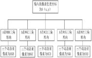
如图3所示,以目前5色块分割法为例,在平面直角坐标系内,RGBYC所在色域可以分割为WBR、WCB、WGC、WYG、WRY这5个三角形色块,三角形色块与动态亚像素的显示颜色具有预设的匹配关系,每一个三角形色块具有对应的动态亚像素的显示颜色。依据输入的像素色度坐标A(x,y)能够确定像素在像素色域中的位置,依据像素在像素色域中的位置,即可确定三个动态亚像素的显示颜色,图4为像素色度坐标A(x,y)的位置与动态亚像素的显示颜色的对应关系图。
根据输入的RGB像素的灰阶值RiGiBi确定动态亚像素的灰阶,i的取值范围为0-255,代表灰阶值。然而不能保证A(x,y)在任意一个三角形色块,当输入的RGB三色信号的灰阶值信号接近相同时,输出亮度和白色色度基本接近,也就是白点的色坐标一致性差。
发明内容
针对上述现有技术中的问题,本申请提出了一种多基色石墨烯显示器的显示方法。
本发明所述的一种多基色石墨烯显示器的显示方法,该方法包括以下步骤:
对像素色域进行分块,以形成多个不同的色块。
依据输入的像素色度坐标,确定像素色度坐标所属的色块。
每一个色块与三个动态亚像素的显示颜色相应,根据像素色度坐标所属的色块,通过三个动态亚像素进行显示。
动态亚像素的输出亮度由白点的坐标、动态亚像素的坐标、输入红色255灰阶时的输出亮度值、输入绿色255灰阶时的输出亮度值和输入蓝色255灰阶时的输出亮度值确定。
本发明中,为了使RGBYC五基色石墨烯显示器具有较好的白点色坐标一致性,对Y色点和C色点进行定义,Y色点为B色点与W色点连接线的延长线与石墨烯发光颜色曲线的交点,C色点为R色点与W色点连接线的延长线与石墨烯发光颜色曲线的交点。
本发明中,在平面直角坐标系内,RGBYC所在色域可以分割为WBR、WCB、WGC、WYG、WRY这5个三角形色块,三角形色块与动态亚像素的显示颜色具有预设的匹配关系,每一个三角形色块具有对应的动态亚像素的显示颜色。
依据输入的像素色度坐标A(x,y)能够确定像素在像素色域中的位置,依据像素在像素色域中的位置,即可确定三个动态亚像素的显示颜色。
利用三个动态亚像素实现RGBYC5基色的超宽色域显示,使得显示具有高色彩饱和度,同时降低了亚像素的数量,因此能够提升显示器的开口率。
本发明中当动态亚像素为RGC或RCB时,R点和C点的输出亮度满足如下公式:
LRg(255)+LCg(255)=LRi(255)+LGi(255)+LBi(255) (1)
XW=[(XRg×LRg/YRg)+(XCg×LCg/YCg)]/(LRg/YRg+LCg/YCg) (2)
Yw=(LRg+LCg)/(LRg/YRg+LCg/YCg) (3)
其中,Xw和Yw分别为W点的横坐标和纵坐标,LRi(255)、LGi(255)和LBi(255)分别为输入红色255灰阶时的输出亮度值、输入绿色255灰阶时的输出亮度值和输入蓝色255灰阶时的输出亮度值,XRg和YRg分别为R点的横坐标和纵坐标,XCg和YCg分别为C点的横坐标和纵坐标,LCg(255)为255灰阶C点输出的亮度值,LRg(255)代表255灰阶R点输出的亮度值。
本发明中当动态亚像素为RGC时,
LGg(255)=a*LGi(255);
其中LGg(255)为255灰阶G点输出的亮度值,0.5<a<2。
优选的是,1≤a≤1.3。
a的最优值为1.2。
本发明中当动态亚像素为RCB时,
LBg(255)=b*LBi(255);
其中LBi(255)为255灰阶B点输出的亮度值,0.5<b<2。
本发明中1≤b≤1.3。
优选的是b=1.2。
本发明中,Xw=0.31,Yw=0.325,LRg(255)为29.3nits,LCg(255)为70.7nits。
本发明中,当动态亚像素为YGB或YRB时,Y点和B点的输出亮度满足如下公式:
LYg(255)+LBg(255)=LRi(255)+LGi(255)+LBi(255) (4)
Xw=[(XBg×LBg/YBg)+(XYg×LYg/YYg)]/(LBg/YBg+LYg/YYg) (5)
Yw=(LBg+LYg)/(LBg/YBg+LYg/YYg) (6)
其中,Xw和Yw分别为W点的横坐标和纵坐标,LRi(255)、LGi(255)和LBi(255)分别为输入红色255灰阶时的输出亮度值、输入绿色255灰阶时的输出亮度值和输入蓝色255灰阶时的输出亮度值,即像素为RGB3基色时,石墨烯显示器输出的255灰阶下R、G、B的亮度值,XBg和YBg分别为B点的横坐标和纵坐标,XYg和YYg分别为Y点的横坐标和纵坐标,LYg(255)为255灰阶Y点输出的亮度值,LBg(255)代表255灰阶B点输出的亮度值。
在本发明的一些实施方案中,石墨烯显示器包括石墨烯显示单元以及显示控制单元。所述显示控制单元与所述石墨烯显示单元之间相互电连接,所述显示控制单元用于控制所述石墨烯显示单元显示相应的颜色及亮度。所述石墨烯显示单元包括下基板、发光结构、保护层、遮光层以及上基板。所述发光结构位于所述下基板的一侧表面,所述保护层覆盖所述发光结构,所述上基板盖设于所述发光结构以及所述保护层上,所述遮光层形成于所述上基板的朝向所述下基板的一侧表面上。
所述下基板以及所述上基板均为玻璃基板,其在透光的同时还为所述石墨烯显示单元提供支撑。所述下基板以及所述上基板也可以采用其他的透明材料,例如,聚对苯二甲酸乙二醇酯(polyethylene terephthalate,PET)或者镍等,另外,所述下基板的材料可以相同,也可以不同。
所述发光结构的数量可以依据所述石墨烯显示器的具体需求而设置。每一个所述发光结构包括发光层、栅极、源极以及漏极。所述栅极覆盖所述发光层朝向所述上基板的一侧表面,所述源极以及所述漏极位于所述发光层背离所述栅极的一侧。所述发光层为半导体还原氧化石墨烯,所述栅极为氧化石墨烯,所述源极
以及所述漏极为还原氧化石墨烯。
实验研究证明,对于石墨烯显示器而言,根据所述栅极电压的不同,所述发光层会发出不同颜色的光,例如,当所述栅极电压Vgs为0-10伏之间,源漏电压Vds大于开启电压Vth时,所述发光单元发出的光为红光;当Vgs为20-30伏之间,源漏电压Vds大于开启电压Vth时,石墨烯发出绿光;当Vgs为40-50伏之间,源漏电压Vds>Vth时,石墨烯发出蓝光。而通过改变Vds电压的大小可以改变所述发光单元发出的光的强弱,从而可以调节灰阶。
因此,每一个所述发光单元实际上构成一个动态像素,可以通过控制源漏电压Vds实现所述发光单元发光颜色的调整,而且每一个所述发光单元不仅能够发出红绿蓝(RGB)三基色光,而且可以发出红绿蓝黄青(RGBYC)五基色甚至更多的颜色。因此,能够实现更鲜艳更广阔的色域覆盖,提高显示显示器开口率、显示器开口率,降低显示功耗。
在一些实施方案中,采用三个所述发光单元组成所述石墨烯显示单元的一个像素,每一个所述发光单元即为所述像素的一个动态亚像素。
在一些实施方案中,仅采用一个发光单元组成所述石墨烯显示单元的一个像素,即每所述石墨烯显示单元的每一个像素只有一个动态亚像素。依据时序驱动方式,同样可以实现多基色全彩广色域显示的目的。
具体地,以RGBYC 5基色180HZ时序驱动为例,首先对像素色域进行时序的划分,将每一个时序匹配所述石墨烯动态亚像素的对应显示颜色。
依据输入的像素色度坐标A(x,y),确定三基色的颜色和显示颜色及时序,依据显示颜色及时序可以调整对应栅极电压Vgs以及源漏电压Vds即可实现时序多基色全彩驱动。
本发明通过对RGBYC5基色不同三角色域的3个动态亚像素亮度进行调整,实现石墨烯显示器具有较好的白点色坐标的一致性,不论A点在哪个三角形色块,当输入的RGB三像素的灰阶值接近相同时,输出亮度和白色色度基本接近,保证白点的色坐标一致性。
上述技术特征可以各种适合的方式组合或由等效的技术特征来替代,只要能够达到本发明的目的。
在下文中将基于实施例并参考附图来对本发明进行更详细的描述。
其中:
图1显示了背景技术中的石墨烯的原子结构图;
图2显示了背景技术中的石墨烯显示器的显示单元的结构示意图;
1为源极,2为栅极,3为发光层,4为漏极,5为下基板,6为上基板,7为反射层;
图3显示了背景技术中的石墨烯显示器的五基色色域在平面直角坐标系的分布图;
图4显示了背景技术中的像素色度坐标A(x,y)的位置与动态亚像素的显示颜色的对应关系图;
图5显示了具体实施方式中石墨烯显示器的五基色色域在平面直角坐标系的分布图;
图6显示了具体实施方式所述的提高RGBYC多基色石墨烯显示器的白点色坐标一致性的方法的流程图。
图7显示了具体实施方式中的像素色度坐标A(x,y)的位置与动态亚像素的显示颜色的对应关系图;
图8显示了具体实施方式中的石墨烯显示器的示意图;
图9显示了具体实施方式中的采用三个石墨烯动态亚像素进行多基色显示的流程图;
图10显示了具体实施方式中的采用一个石墨烯动态亚像素进行多基色显示的流程图。
附图并未按照实际的比例。
为了使本技术领域的人员更好地理解本发明中的技术方案,下面将结合本发明实施例中的附图,对本发明实施例中的技术方案进行清楚、完整地描述,显然,所描述的实施例仅仅是本发明一部分实施例,而不是全部的实施例。基于本发明中的实施例,本领域普通技术人员在没有做出创造性劳动前提下所获得的所有其他实施例,都应当属于本发明保护的范围。
本发明提供一种多基色石墨烯显示器的显示方法,该方法包括以下步骤:
对像素色域进行分块,以形成多个不同的色块;
依据输入的像素色度坐标,确定像素色度坐标所属的色块;
每一个色块与三个动态亚像素的显示颜色相应,根据像素色度坐标所属的色块,通过三个动态亚像素进行显示;
动态亚像素的输出亮度由白点的坐标、动态亚像素的坐标、输入红色255灰阶时的输出亮度值、输入绿色255灰阶时的输出亮度值和输入蓝色255灰阶时的输出亮度值确定。
本实施方式中,Y色点为B色点与W色点连接线的延长线与石墨烯发光颜色曲线的交点,C色点为R色点与W色点连接线的延长线与石墨烯发光颜色曲线的交点。
在RGB3基色体系中,首先定义石墨烯显示器的RGB的坐标(石墨烯显示器的色彩峰值波长WP可通过门电压Vg的大小来进行调节),若白点色坐标为Xw=0.31,Yw=0.325,RGB均为255灰阶,RGB的亮度分别为20.6nits,75.2nits,4.2nits,RGB的WP及坐标见表1,255灰阶下RGB的亮度值见表2。
表1 RGB的色度坐标及WP值
| 像素 | Vg(V) | WP(nm) | 横坐标 | 纵坐标 |
| R | 0 | 650 | 0.7032 | 0.2967 |
| G | 25 | 530 | 0.2096 | 0.7037 |
| B | 45 | 450 | 0.1488 | 0.0339 |
表2 RGB的亮度值
| 像素 | 灰阶值 | 亮度(nits) |
| R | 255 | 20.6 |
| G | 255 | 75.2 |
| B | 255 | 4.2 |
| 亮度总和 | 100 |
为了使RGBYC五基色石墨烯显示器具有较好的白点色坐标一致性,对Y色点
和C色点进行定义,其中Y色点为B色点与W色点连接线的延长线与石墨烯发光颜色曲线的交点,C色点为R色点与W色点连接线的延长线与石墨烯发光颜色曲线的交点。
在平面直角坐标系内,RGBYC所在色域可以分割为WBR、WCB、WGC、WYG、WRY这5个三角形色块,三角形色块与动态亚像素的显示颜色具有预设的匹配关系,每一个三角形色块具有对应的动态亚像素的显示颜色。
依据输入的像素色度坐标A(x,y)能够确定像素在像素色域中的位置,依据像素在像素色域中的位置,即可确定三个动态亚像素的显示颜色,图7为像素色度坐标A(x,y)的位置与动态亚像素的显示颜色的对应关系图。
采用以上方式,即可利用三个动态亚像素实现RGBYC5基色的超宽色域显示,使得显示具有高色彩饱和度,同时降低了亚像素的数量,因此能够提升显示器的开口率。
本实施方式的石墨烯显示器,包括石墨烯显示单元以及显示控制单元。所述显示控制单元与所述石墨烯显示单元之间相互电连接,所述显示控制单元用于控制所述石墨烯显示单元显示相应的颜色及亮度。
所述石墨烯显示单元包括下基板、发光结构、保护层、遮光层以及上基板。所述发光结构位于所述下基板的一侧表面,所述保护层覆盖所述发光结构,所述上基板盖设于所述发光结构以及所述保护层上,所述遮光层形成于所述上基板的朝向所述下基板的一侧表面上。
本实施方式中,所述下基板以及所述上基板均为玻璃基板,其在透光的同时还为所述石墨烯显示单元提供支撑。可以理解,在其他的实施例中,所述下基板以及所述上基板也可以采用其他的透明材料,例如,聚对苯二甲酸乙二醇酯(polyethylene terephthalate,PET)或者镍等,另外,所述上基板与下基板的材料可以相同,也可以不同。
所述发光结构的数量可以依据所述石墨烯显示器的具体需求而设置。每一个所述发光结构包括发光层、栅极、源极以及漏极。所述栅极覆盖所述发光层朝向所述上基板的一侧表面,所述源极以及所述漏极位于所述发光层背离所述栅极的一侧。本实施例中,所述发光层为半导体还原氧化石墨烯,所述栅极为氧化石墨烯,所述源极以及所述漏极为还原氧化石墨烯。
实验研究证明,对于石墨烯显示器而言,根据所述栅极电压的不同,所述发
光层会发出不同颜色的光,例如,当所述栅极电压Vgs为0-10伏之间,源漏电压Vds大于开启电压Vth时,所述发光单元发出的光为红光;当Vgs为20-30伏之间,源漏电压Vds大于开启电压Vth时,石墨烯发出绿光;当Vgs为40-50伏之间,源漏电压Vds>Vth时,石墨烯发出蓝光。而通过改变Vds电压的大小可以改变所述发光单元发出的光的强弱,从而可以调节灰阶。
因此,每一个所述发光单元实际上构成一个动态像素,可以通过控制源漏电压Vds实现所述发光单元发光颜色的调整,而且每一个所述发光单元不仅能够发出红绿蓝(RGB)三基色光,而且可以发出红绿蓝黄青(RGBYC)五基色甚至更多的颜色。因此,能够实现更鲜艳更广阔的色域覆盖,提高显示显示器开口率、显示器开口率,降低显示功耗。
可以采用三个所述发光单元组成所述石墨烯显示单元的一个像素,每一个所述发光单元即为所述像素的一个动态亚像素。
此外,可以仅采用一个发光单元组成所述石墨烯显示单元的一个像素,即所述石墨烯显示单元的每一个像素只有一个动态亚像素。依据时序驱动方式,同样可以实现多基色全彩广色域显示的目的。
具体地,以RGBYC 5基色180HZ时序驱动为例,首先对像素色域进行时序的划分,将每一个时序匹配所述石墨烯动态亚像素的对应显示颜色。
依据输入的像素色度坐标A(x,y),确定三基色的颜色和显示颜色及时序,依据显示颜色及时序可以调整对应栅极电压Vgs以及源漏电压Vds即可实现时序多基色全彩驱动。
将每秒按时序分割若干等分,在每一个分割的时序内依据对应显示颜色调整栅极电压Vgs以及源漏电压Vds,三个相邻时序显示的颜色构成三基色,依据该时序的输入控制栅极电压Vgs为以及源漏电压Vds以预定灰阶显示第一颜色,在下一时序时,依据该时序的输入控制栅极电压Vgs为以及源漏电压Vds以预定灰阶显示第二颜色,在接下来的时序,依据该时序的输入控制栅极电压Vgs为以及源漏电压Vds以预定灰阶显示第三颜色,此三个时序的光在视觉上可以混合形成预定颜色的光。
因此,实现了一个像素中依靠单动态亚像素显示多基色全彩广色域显示的目的,此种显示器能够减少石墨烯显示单元中像素的数量,提升开口率,并降低显示功耗。此种显示器驱动方式,能够进一步减少石墨烯显示单元中像素的数量,
提升开口率,并降低显示功耗。
保护层用于保护所述发光结构,防止水、气及其他杂质入侵对所述发光结构造成损坏。
所述发光结构的材料为二氧化硅(SiO2)。
所述遮光层用于防止背景光泄漏,以提高显示对比度,防止混色和增加颜色的纯度。所述遮光层为形成于发光结构之间的不透光部分,对应于发光结构,所述遮光层具有贯穿的透光窗,使得所述遮光层的分布呈矩阵状,因此,所述遮光层又称为黑色矩阵层。可选地,所述遮光层为沉积于所述上基板表面上的铬材料层,具体地,首先在所述第二透明基板上溅射形成铬层,然后采用光刻法蚀刻形成所述透光窗。此外,也可以采用含有黑色染料的树脂光刻胶,用光刻法形成所述遮光层。
所述石墨烯显示器还包括反射层,所述反射层形成于所述下基板背离所述发光结构的一侧表面上。所述反射层能够反射所述发光结构的光,提高光线的利用率。
优选地,所述反射层采用高反射率金属材料制成。
所述显示控制单元用于依据输入RGB像素的灰阶值以及像素色度坐标控制所述石墨烯显示单元的动态亚像素进行相应的显示。
以三个动态亚像素实现五基色显示为例,所述显示控制单元首先需对像素色域进行划分,将像素色域划分为五个三角形色块,并匹配对应的像素色度坐标和显示颜色的关系;
具体地,在平面直角坐标系内,所述像素色域被划分成WBR、WCB、WGC、WYG、WRY五个三角形色块,每一个三角形色块对应动态像素所显示的颜色,所述像素色度坐标被标记为A(x,y),所述像素色度坐标落入对应的三角形色块时,所述显示控制单元即控制所述动态亚像素以对应的颜色显示,进而实现三个动态亚像素进行五基色显示。
对于一个动态亚像素实现五基色显示的情况,所述显示控制单元首先对像素色域进行时序的划分,将每一个时序匹配所述石墨烯动态亚像素的对应显示颜色,所述显示控制单元依据输入的RGB像素灰阶值RiGiBi以及像素色度坐标A(x,y)进行彩色转换并确定显示的颜色及时序,选择时序对应的漏源电压Vds及栅极电压Vgs进行颜色及亮度显示。为了保证白点的色坐标一致性当输入的
RGB三像素的灰阶值接近相同时,动态亚像素的输出亮度由W点即白点的坐标、动态亚像素的坐标、输入红色255灰阶时的输出亮度值、输入绿色255灰阶时的输出亮度值和输入蓝色255灰阶时的输出亮度值确定。
所述石墨烯显示器通过驱动动态像素能够以较少的像素实现多基色显示,实现所述石墨烯显示器具有更为鲜艳、广阔的色域覆盖,提高所述石墨烯显示的开口率并降低功耗。
如图9,所示为具体地采用三个石墨烯动态亚像素进行多基色显示的流程图,
其包括如下步骤:
步骤A1,在平面直角坐标系内对像素色域进行多基色显示区域的划分,将每一个显示区域匹配所述石墨烯动态亚像素的对应显示颜色。
具体地,在一平面直角坐标系内,像素色域被分为WBR、WCB、WGC、WYG、WRY五个三角形色块,所述三角形色块与所述动态亚像素的显示颜色具有预设的匹配关系,每一个所述三角形色块具有对应的所述动态亚像素的显示颜色。
步骤A2,依据输入的像素色度坐标A(x,y),判断所述像素坐标在所述像素色域的位置,并依据所述位置控制所述石墨烯动态亚像素进行显示。为了保证白点的色坐标一致性当输入的RGB三像素的灰阶值接近相同时,动态亚像素的输出亮度由W点即白点的坐标、动态亚像素的坐标、输入红色255灰阶时的输出亮度值、输入绿色255灰阶时的输出亮度值和输入蓝色255灰阶时的输出亮度值确定。
采用以上方式,即可利用三个动态亚像素实现5基色的超宽色域显示,使得显示具有高色彩饱和度,同时降低了亚像素的数量,因此能够提升显示器的开口率。
如图10,所示为采用一个石墨烯动态亚像素进行多基色显示的流程图,
其包括如下步骤:
步骤B1,对像素色域进行时序划分,将每一个时序代表匹配所述石墨烯动态亚像素的对应显示颜色。
以180Hz时序驱动为例,将每秒按时序分割180等分,在每一个分割的时序内依据对应显示颜色调整栅极电压Vgs以及源漏电压Vds,三个相邻时序显示的颜色构成三基色,例如,在1/180秒时,依据该时序的输入控制栅极电压Vgs为以及源漏电压Vds以预定灰阶显示第一颜色,在2/180秒时,依据该时序的输入控制栅极电压Vgs为以及源漏电压Vds以预定灰阶显示第二颜色,在3/180秒
时,依据该时序的输入控制栅极电压Vgs为以及源漏电压Vds以预定灰阶显示第三颜色,此三个时序的光在视觉上可以混合形成预定颜色的光。
步骤B2,依据输入的像素色度坐标,判断所述像素色度坐标对应的时序及颜色,并依据所述位置控制所述石墨烯动态亚像素进行显示。为了保证白点的色坐标一致性当输入的RGB三像素的灰阶值接近相同时,动态亚像素的输出亮度由W点即白点的坐标、动态亚像素的坐标、输入红色255灰阶时的输出亮度值、输入绿色255灰阶时的输出亮度值和输入蓝色255灰阶时的输出亮度值确定。
本实施方式中,
当动态亚像素为RGC或RCB时,R点和C点的输出亮度满足如下公式:
LRg(255)+LCg(255)=LRi(255)+LGi(255)+LBi(255) (1)
Xw=[(XRg×LRg/YRg)+(XCg×LCg/YCg)]/(LRg/YRg+LCg/YCg) (2)
Yw=(LRg+LCg)/(LRg/YRg+LCg/YCg) (3)
其中,Xw和Yw分别为W点的横坐标和纵坐标,LRi(255)、LGi(255)和LBi(255)分别为输入红色255灰阶时的输出亮度值、输入绿色255灰阶时的输出亮度值和输入蓝色255灰阶时的输出亮度值,XRg和YRg分别为R点的横坐标和纵坐标,XCg和YCg分别为C点的横坐标和纵坐标,LCg(255)为255灰阶C点输出的亮度值,LRg(255)代表255灰阶R点输出的亮度值。
本实施方式中,当动态亚像素为RGC时,
LGg(255)=a*LGi(255);
其中LGg(255)为255灰阶G点输出的亮度值,0.5<a<2。
本实施方式中,1≤a≤1.3。
a的优选值为1-1.3,a的最优值为1.2。
本实施方式中,当动态亚像素为RCB时,
LBg(255)=b*LBi(255);
其中LBi(255)为255灰阶B点输出的亮度值,0.5<b<2。
本实施方式中,1≤b≤1.3。
b的优选值为1-1.3,b的最优值为1.2。
本实施方式中,Xw=0.31,Yw=0.325,LRg(255)为29.3nits,LCg(255)为70.7nits。
本实施方式中,当动态亚像素为YGB或YRB时,Y点和B点的输出亮度满足如下
公式:
LYg(255)+LBg(255)=LRi(255)+LGi(255)+LBi(255) (4)
Xw=[(XBg×LBg/YBg)+(XYg×LYg/YYg)]/(LBg/YBg+LYg/YYg) (5)
Yw=(LBg+LYg)/(LBg/YBg+LYg/YYg) (6)
其中,Xw和Yw分别为W点的横坐标和纵坐标,LRi(255)、LGi(255)和LBi(255)分别为输入红色255灰阶时的输出亮度值、输入绿色255灰阶时的输出亮度值和输入蓝色255灰阶时的输出亮度值,XBg和YBg分别为B点的横坐标和纵坐标,XYg和YYg分别为Y点的横坐标和纵坐标,LYg(255)为255灰阶Y点输出的亮度值,LBg(255)代表255灰阶B点输出的亮度值。
本实施方式中,Xw=0.31,Yw=0.325,LBg(255)为4.6nits,LYg(255)为95.4nits。
对于本领域技术人员而言,显然本发明不限于上述示范性实施例的细节,而且在不背离本发明的精神或基本特征的情况下,能够以其他的具体形式实现本发明。因此,无论从哪一点来看,均应将实施例看作是示范性的,而且是非限制性的,本发明的范围由所附权利要求而不是上述说明限定,因此旨在将落在权利要求的等同要件的含义和范围内的所有变化囊括在本发明内。
虽然在本文中参照了特定的实施方式来描述本发明,但是应该理解的是,这些实施例仅仅是本发明的原理和应用的示例。因此应该理解的是,可以对示例性的实施例进行许多修改,并且可以设计出其他的布置,只要不偏离所附权利要求所限定的本发明的精神和范围。应该理解的是,可以通过不同于原始权利要求所描述的方式来结合不同的从属权利要求和本文中所述的特征。还可以理解的是,结合单独实施例所描述的特征可以使用在其他所述实施例中。
Claims (12)
- 一种多基色石墨烯显示器的显示方法,其中,该方法包括以下步骤:对像素色域进行分块,以形成多个不同的色块;依据输入的像素色度坐标,确定像素色度坐标所属的色块;每一个色块与三个动态亚像素的显示颜色相应,根据像素色度坐标所属的色块,通过三个动态亚像素进行显示;动态亚像素的输出亮度由白点的坐标、动态亚像素的坐标、输入红色255灰阶时的输出亮度值、输入绿色255灰阶时的输出亮度值和输入蓝色255灰阶时的输出亮度值确定。
- 如权利要求1所述的方法,其中,Y色点为B色点与W色点连接线的延长线与石墨烯发光颜色曲线的交点,C色点为R色点与W色点连接线的延长线与石墨烯发光颜色曲线的交点;像素色域被分为WBR、WCB、WGC、WYG、WRY五个三角形色块,每一个所述三角形色块具有对应的三个动态亚像素的显示颜色。
- 如权利要求2所述的方法,其中,当动态亚像素为RGC或RCB时,R点和C点的输出亮度满足如下公式:LRg(255)+LCg(255)=LRi(255)+LGi(255)+LBi(255) (1)XW=[(XRg×LRg/YRg)+(XCg×LCg/YCg)]/(LRg/YRg+LCg/YCg) (2)Yw=(LRg+LCg)/(LRg/YRg+LCg/YCg) (3)其中,Xw和Yw分别为W点的横坐标和纵坐标,LRi(255)、LGi(255)和LBi(255)分别为输入红色255灰阶时的输出亮度值、输入绿色255灰阶时的输出亮度值和输入蓝色255灰阶时的输出亮度值,XRg和YRg分别为R点的横坐标和纵坐标,XCg和YCg分别为C点的横坐标和纵坐标,LCg(255)为255灰阶C点输出的亮度值,LRg(255)代表255灰阶R点输出的亮度值。
- 如权利要求3所述的方法,其中,当动态亚像素为RGC时,LGg(255)=a*LGi(255);其中LGg(255)为255灰阶G点输出的亮度值,0.5<a<2。
- 如权利要求4所述的方法,其中,1≤a≤1.3。
- 如权利要求5所述的方法,其中,a为1.2。
- 如权利要求3所述的方法,其中,当动态亚像素为RCB时,LBg(255)=b*LBi(255);其中LBi(255)为255灰阶B点输出的亮度值,0.5<b<2。
- 如权利要求7所述的方法,其中,1≤b≤1.3。
- 如权利要求8所述的方法,其中,b=1.2。
- 如权利要求3所述的方法,其中,Xw=0.31,Yw=0.325,LRg(255)为29.3nits,LCg(255)为70.7nits。
- 如权利要求2所述的方法,其中,当动态亚像素为YGB或YRB时,Y点和B点的输出亮度满足如下公式:LYg(255)+LBg(255)=LRi(255)+LGi(255)+LBi(255) (4)Xw=[(XBg×LBg/YBg)+(XYg×LYg/YYg)]/(LBg/YBg+LYg/YYg) (5)Yw=(LBg+LYg)/(LBg/YBg+LYg/YYg) (6)其中,Xw和Yw分别为W点的横坐标和纵坐标,LRi(255)、LGi(255)和LBi(255)分别为输入红色255灰阶时的输出亮度值、输入绿色255灰阶时的输出亮度值和输入蓝色255灰阶时的输出亮度值,XBg和YBg分别为B点的横坐标和纵坐标,XYg和YYg分别为Y点的横坐标和纵坐标,LYg(255)为255灰阶Y点输出的亮度值,LBg(255)代表255灰阶B点输出的亮度值。
- 如权利要求11所述的方法,其中,Xw=0.31,Yw=0.325,LBg(255)为4.6nits,LYg(255)为95.4nits。
Priority Applications (1)
| Application Number | Priority Date | Filing Date | Title |
|---|---|---|---|
| US15/328,518 US10410588B2 (en) | 2016-11-01 | 2017-01-05 | Display method of multi-primary color graphene display device |
Applications Claiming Priority (2)
| Application Number | Priority Date | Filing Date | Title |
|---|---|---|---|
| CN201610937011.1 | 2016-11-01 | ||
| CN201610937011.1A CN106486074B (zh) | 2016-11-01 | 2016-11-01 | 多基色石墨烯显示器的显示方法 |
Publications (1)
| Publication Number | Publication Date |
|---|---|
| WO2018082207A1 true WO2018082207A1 (zh) | 2018-05-11 |
Family
ID=58271431
Family Applications (1)
| Application Number | Title | Priority Date | Filing Date |
|---|---|---|---|
| PCT/CN2017/070282 Ceased WO2018082207A1 (zh) | 2016-11-01 | 2017-01-05 | 多基色石墨烯显示器的显示方法 |
Country Status (3)
| Country | Link |
|---|---|
| US (1) | US10410588B2 (zh) |
| CN (1) | CN106486074B (zh) |
| WO (1) | WO2018082207A1 (zh) |
Cited By (1)
| Publication number | Priority date | Publication date | Assignee | Title |
|---|---|---|---|---|
| CN111816114A (zh) * | 2020-08-17 | 2020-10-23 | 京东方科技集团股份有限公司 | 显示面板调光装置及调光方法、显示面板及其驱动方法 |
Families Citing this family (5)
| Publication number | Priority date | Publication date | Assignee | Title |
|---|---|---|---|---|
| CN107492365B (zh) * | 2017-09-27 | 2020-07-03 | 深圳市华星光电半导体显示技术有限公司 | 获得色域映射拟合函数的方法及装置 |
| CN107945729B (zh) * | 2017-12-15 | 2020-05-08 | 京东方科技集团股份有限公司 | 转换方法及电路、显示装置及驱动方法和电路、存储介质 |
| CN108388060B (zh) * | 2018-03-13 | 2022-05-13 | 京东方科技集团股份有限公司 | 发光显示基板、显示面板及其控制方法、显示装置 |
| JP2022036839A (ja) * | 2020-08-24 | 2022-03-08 | セイコーエプソン株式会社 | 画像処理装置、画像処理方法および画像処理プログラム |
| CN112562604A (zh) * | 2020-12-01 | 2021-03-26 | 惠科股份有限公司 | 显示装置及其灰阶控制方法 |
Citations (6)
| Publication number | Priority date | Publication date | Assignee | Title |
|---|---|---|---|---|
| US20080122861A1 (en) * | 2006-11-27 | 2008-05-29 | Texas Instruments Incorporated | System and method to generate multiprimary signals |
| CN105303985A (zh) * | 2015-11-24 | 2016-02-03 | 深圳市华星光电技术有限公司 | 石墨烯显示器及其显示驱动方法 |
| CN105702220A (zh) * | 2016-04-06 | 2016-06-22 | 深圳市华星光电技术有限公司 | 石墨烯显示器的驱动方法以及石墨烯显示器 |
| CN105825829A (zh) * | 2016-05-18 | 2016-08-03 | 深圳市华星光电技术有限公司 | 石墨烯显示器以及石墨烯显示器的驱动方法、驱动装置 |
| CN105869589A (zh) * | 2016-05-27 | 2016-08-17 | 深圳市华星光电技术有限公司 | 石墨烯显示器以及石墨烯显示器的驱动方法、驱动装置 |
| CN106057120A (zh) * | 2016-08-15 | 2016-10-26 | 深圳市华星光电技术有限公司 | 一种显示器彩色转换方法 |
Family Cites Families (15)
| Publication number | Priority date | Publication date | Assignee | Title |
|---|---|---|---|---|
| EP1407445B1 (en) * | 2001-06-07 | 2010-07-21 | Genoa Color Technologies Ltd. | System and method of data conversion for wide gamut displays |
| KR100441595B1 (ko) * | 2001-10-15 | 2004-07-23 | 삼성전자주식회사 | 색온도 변환장치 및 방법 |
| JP2007529778A (ja) * | 2004-03-19 | 2007-10-25 | コーニンクレッカ フィリップス エレクトロニクス エヌ ヴィ | 低輝度での画素間の非均一性改善を伴うアクティブマトリクスディスプレイ |
| US20090040564A1 (en) * | 2006-01-21 | 2009-02-12 | Iq Colour, Llc | Vision-Based Color and Neutral-Tone Management |
| TW200828203A (en) * | 2006-12-29 | 2008-07-01 | Innolux Display Corp | Six primary-color display |
| US20100225673A1 (en) * | 2009-03-04 | 2010-09-09 | Miller Michael E | Four-channel display power reduction with desaturation |
| US8466856B2 (en) * | 2011-02-22 | 2013-06-18 | Global Oled Technology Llc | OLED display with reduced power consumption |
| US8237633B2 (en) * | 2009-05-12 | 2012-08-07 | Global Oled Technology Llc | Electro-luminescent display with adjustable white point |
| US9049410B2 (en) * | 2009-12-23 | 2015-06-02 | Samsung Display Co., Ltd. | Color correction to compensate for displays' luminance and chrominance transfer characteristics |
| US8830256B2 (en) * | 2009-12-23 | 2014-09-09 | Samsung Display Co., Ltd. | Color correction to compensate for displays' luminance and chrominance transfer characteristics |
| CN104981861B (zh) * | 2013-02-14 | 2017-04-12 | 三菱电机株式会社 | 信号转换装置和方法 |
| TWI550593B (zh) * | 2013-08-14 | 2016-09-21 | 友達光電股份有限公司 | 顯示裝置 |
| KR20150022235A (ko) * | 2013-08-22 | 2015-03-04 | 삼성디스플레이 주식회사 | 색 보상 장치와 이를 포함하는 표시 장치, 및 색 보상 방법 |
| CN104485075A (zh) * | 2014-12-30 | 2015-04-01 | 广东威创视讯科技股份有限公司 | 发光元件显示屏的混色方法 |
| KR102278243B1 (ko) * | 2015-02-25 | 2021-07-19 | 한국전자통신연구원 | 전기변색 소자 |
-
2016
- 2016-11-01 CN CN201610937011.1A patent/CN106486074B/zh active Active
-
2017
- 2017-01-05 US US15/328,518 patent/US10410588B2/en not_active Expired - Fee Related
- 2017-01-05 WO PCT/CN2017/070282 patent/WO2018082207A1/zh not_active Ceased
Patent Citations (6)
| Publication number | Priority date | Publication date | Assignee | Title |
|---|---|---|---|---|
| US20080122861A1 (en) * | 2006-11-27 | 2008-05-29 | Texas Instruments Incorporated | System and method to generate multiprimary signals |
| CN105303985A (zh) * | 2015-11-24 | 2016-02-03 | 深圳市华星光电技术有限公司 | 石墨烯显示器及其显示驱动方法 |
| CN105702220A (zh) * | 2016-04-06 | 2016-06-22 | 深圳市华星光电技术有限公司 | 石墨烯显示器的驱动方法以及石墨烯显示器 |
| CN105825829A (zh) * | 2016-05-18 | 2016-08-03 | 深圳市华星光电技术有限公司 | 石墨烯显示器以及石墨烯显示器的驱动方法、驱动装置 |
| CN105869589A (zh) * | 2016-05-27 | 2016-08-17 | 深圳市华星光电技术有限公司 | 石墨烯显示器以及石墨烯显示器的驱动方法、驱动装置 |
| CN106057120A (zh) * | 2016-08-15 | 2016-10-26 | 深圳市华星光电技术有限公司 | 一种显示器彩色转换方法 |
Cited By (2)
| Publication number | Priority date | Publication date | Assignee | Title |
|---|---|---|---|---|
| CN111816114A (zh) * | 2020-08-17 | 2020-10-23 | 京东方科技集团股份有限公司 | 显示面板调光装置及调光方法、显示面板及其驱动方法 |
| CN111816114B (zh) * | 2020-08-17 | 2023-09-29 | 京东方科技集团股份有限公司 | 显示面板调光装置及调光方法、显示面板及其驱动方法 |
Also Published As
| Publication number | Publication date |
|---|---|
| CN106486074A (zh) | 2017-03-08 |
| US10410588B2 (en) | 2019-09-10 |
| CN106486074B (zh) | 2019-04-02 |
| US20180336833A1 (en) | 2018-11-22 |
Similar Documents
| Publication | Publication Date | Title |
|---|---|---|
| WO2017088284A1 (zh) | 石墨烯显示器及其显示驱动方法 | |
| WO2018082207A1 (zh) | 多基色石墨烯显示器的显示方法 | |
| CN106057120B (zh) | 一种显示器彩色转换方法 | |
| US9368062B2 (en) | Display panel display device including the display panel and method for driving the display panel | |
| CN113196160A (zh) | 阵列基板及其制作方法、显示装置以及显示基板 | |
| CN105869589B (zh) | 石墨烯显示器以及石墨烯显示器的驱动方法、驱动装置 | |
| CN105280684B (zh) | 一种oled显示面板及其制备方法 | |
| CN1809936A (zh) | 具有增进效率的堆叠式有机发光二极管显示器 | |
| KR20070094679A (ko) | 컬러필터 기판 | |
| KR102121627B1 (ko) | 디스플레이 장치 및 그 제조 방법 | |
| CN100559440C (zh) | 降低平面显示器功率消耗的驱动方法 | |
| CN105576004A (zh) | 一种量子点彩色光转换膜、oled面板及显示装置 | |
| WO2019100420A1 (zh) | 显示面板及具有该显示面板的显示装置 | |
| CN102760837B (zh) | 有机发光二极管器件结构及显示装置 | |
| CN105702220B (zh) | 石墨烯显示器的驱动方法以及石墨烯显示器 | |
| CN104966492A (zh) | 显示装置的驱动方法 | |
| CN105702697B (zh) | 石墨烯显示器 | |
| CN103676220B (zh) | 显示装置及其制造方法 | |
| CN105825829B (zh) | 石墨烯显示器以及石墨烯显示器的驱动方法、驱动装置 | |
| JP2004227854A (ja) | エレクトロルミネッセンス表示装置 | |
| CN106711255B (zh) | 光致发光显示面板 | |
| CN105789265B (zh) | 一种显示装置 | |
| CN106960896A (zh) | 一种光掩膜版以及石墨烯发光显示器件的制备方法 | |
| CN109616502A (zh) | 显示面板 | |
| Chen et al. | 70.3: Low power consumption and wide color gamut amoled display with four primary colors |
Legal Events
| Date | Code | Title | Description |
|---|---|---|---|
| WWE | Wipo information: entry into national phase |
Ref document number: 15328518 Country of ref document: US |
|
| 121 | Ep: the epo has been informed by wipo that ep was designated in this application |
Ref document number: 17867211 Country of ref document: EP Kind code of ref document: A1 |
|
| NENP | Non-entry into the national phase |
Ref country code: DE |
|
| 122 | Ep: pct application non-entry in european phase |
Ref document number: 17867211 Country of ref document: EP Kind code of ref document: A1 |