WO2018074041A1 - 研磨パッドの表面性状測定装置 - Google Patents
研磨パッドの表面性状測定装置 Download PDFInfo
- Publication number
- WO2018074041A1 WO2018074041A1 PCT/JP2017/029154 JP2017029154W WO2018074041A1 WO 2018074041 A1 WO2018074041 A1 WO 2018074041A1 JP 2017029154 W JP2017029154 W JP 2017029154W WO 2018074041 A1 WO2018074041 A1 WO 2018074041A1
- Authority
- WO
- WIPO (PCT)
- Prior art keywords
- polishing
- light
- polishing pad
- receiving sensor
- light receiving
- Prior art date
- Legal status (The legal status is an assumption and is not a legal conclusion. Google has not performed a legal analysis and makes no representation as to the accuracy of the status listed.)
- Ceased
Links
Images



Classifications
-
- B—PERFORMING OPERATIONS; TRANSPORTING
- B24—GRINDING; POLISHING
- B24B—MACHINES, DEVICES, OR PROCESSES FOR GRINDING OR POLISHING; DRESSING OR CONDITIONING OF ABRADING SURFACES; FEEDING OF GRINDING, POLISHING, OR LAPPING AGENTS
- B24B37/00—Lapping machines or devices; Accessories
- B24B37/34—Accessories
-
- B—PERFORMING OPERATIONS; TRANSPORTING
- B24—GRINDING; POLISHING
- B24B—MACHINES, DEVICES, OR PROCESSES FOR GRINDING OR POLISHING; DRESSING OR CONDITIONING OF ABRADING SURFACES; FEEDING OF GRINDING, POLISHING, OR LAPPING AGENTS
- B24B49/00—Measuring or gauging equipment for controlling the feed movement of the grinding tool or work; Arrangements of indicating or measuring equipment, e.g. for indicating the start of the grinding operation
- B24B49/12—Measuring or gauging equipment for controlling the feed movement of the grinding tool or work; Arrangements of indicating or measuring equipment, e.g. for indicating the start of the grinding operation involving optical means
-
- G—PHYSICS
- G01—MEASURING; TESTING
- G01B—MEASURING LENGTH, THICKNESS OR SIMILAR LINEAR DIMENSIONS; MEASURING ANGLES; MEASURING AREAS; MEASURING IRREGULARITIES OF SURFACES OR CONTOURS
- G01B11/00—Measuring arrangements characterised by the use of optical techniques
- G01B11/30—Measuring arrangements characterised by the use of optical techniques for measuring roughness or irregularity of surfaces
-
- H—ELECTRICITY
- H10—SEMICONDUCTOR DEVICES; ELECTRIC SOLID-STATE DEVICES NOT OTHERWISE PROVIDED FOR
- H10P—GENERIC PROCESSES OR APPARATUS FOR THE MANUFACTURE OR TREATMENT OF DEVICES COVERED BY CLASS H10
- H10P52/00—Grinding, lapping or polishing of wafers, substrates or parts of devices
Definitions
- the present invention relates to a surface property measuring apparatus for a polishing pad that measures surface properties such as a surface shape and a surface state of a polishing pad used for polishing a substrate such as a semiconductor wafer.
- CMP chemical mechanical polishing
- the polishing apparatus that performs the CMP described above includes a polishing table having a polishing pad and a substrate holding device called a carrier or top ring for holding a semiconductor wafer (substrate). While holding a substrate with a substrate holding device using such a polishing apparatus, the substrate is pressed against the polishing pad with a predetermined pressure to polish an insulating film or a metal film on the substrate. Yes.
- polishing pad When the substrate is polished, abrasive grains and polishing debris adhere to the surface of the polishing pad, and the surface shape and state of the polishing pad change to deteriorate the polishing performance. For this reason, as the polishing of the substrate is repeated, the polishing rate decreases and uneven polishing occurs. Therefore, dressing (conditioning) of the polishing pad is performed using a dresser in order to regenerate the surface shape and state of the deteriorated polishing pad.
- Non-Patent Documents 1 and 2 suggest that the surface shape characteristics of the polishing pad can be measured by irradiating the surface of the polishing pad with laser light and optically analyzing the scattered reflected light. .
- the present invention has been made in view of the above-described circumstances, and includes a polishing pad surface property measuring apparatus capable of accurately measuring the surface property of the polishing pad by eliminating the influence of various disturbances and the like, and the measuring device.
- An object of the present invention is to provide a polishing apparatus.
- one embodiment of the present invention is a surface property measuring apparatus for a polishing pad used for polishing a substrate, which includes a housing that does not transmit light, and an optical that is attached to the casing.
- a window a laser light source that emits a laser beam, an incident light mirror that guides the laser beam to the polishing pad through the optical window, and a light receiving sensor that measures the intensity of scattered light generated when the laser beam hits the polishing pad;
- the laser light source, the incident light mirror, and the light receiving sensor are arranged in the housing.
- a vertical movement mechanism for moving the light receiving sensor up and down is further provided.
- the vertical movement mechanism raises the light receiving sensor to a position where the light receiving sensor can receive nth order light (n is a predetermined natural number) from the 0th order light of the scattered light. And / or lowering.
- the apparatus further includes a jet nozzle that sends a gas jet to the polishing surface of the polishing pad, and the jet nozzle is fixed to the casing.
- a preferred aspect of the present invention is further characterized by further comprising a band pass filter disposed between the optical window and the light receiving sensor.
- the bandpass filter is configured to pass only light having a wavelength within a limited range including the wavelength of the laser beam.
- a preferred aspect of the present invention is characterized by further comprising a neutral density filter disposed between the laser light source and the optical window.
- a polarizing filter is further provided between the laser light source and the optical window.
- the apparatus further includes a translation mechanism that moves the casing in a plane parallel to the polishing surface of the polishing pad.
- a preferred aspect of the present invention is characterized by further comprising a scattered light mirror that reflects scattered light from the polishing pad and guides it to the light receiving sensor.
- the scattered light mirror is a concave mirror.
- One aspect of the present invention includes a polishing table that supports a polishing pad, a polishing head that presses a substrate against the polishing pad, and the surface property measuring apparatus that measures the surface property of the polishing pad. It is a polishing apparatus.
- the housing can not only protect the optical system including the laser light source and the light receiving sensor from liquids such as slurry and pure water, but also can block light other than the laser beam. Therefore, the surface texture measuring apparatus can accurately measure the surface texture of the polishing pad by eliminating the influence of various disturbances.
- the vertical movement mechanism can move the light receiving sensor to an optimal position where the light receiving sensor can receive scattered light from the 0th order light to the nth order light. Therefore, the surface texture measuring device can accurately measure the surface texture of the polishing pad.
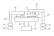
- FIG. 2 is a side view of the polishing apparatus shown in FIG. It is sectional drawing of a measurement head. It is a figure which shows the spectrum of scattered light. It is a figure which shows the range of the scattered light which a light receiving sensor can receive when a light receiving sensor exists in a position too low. It is a figure which shows the range of the scattered light which a light receiving sensor can receive when a light receiving sensor exists in a position too high. It is a figure which shows other embodiment of a measurement head. It is a figure which shows embodiment which fixed the measurement head to the dresser arm. It is a figure which shows embodiment which fixed the measurement head to the grinding
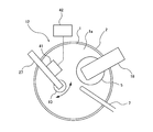
- FIG. 1 is a schematic plan view showing an embodiment of a polishing apparatus equipped with a surface texture measuring device for a polishing pad.
- the polishing apparatus selectively uses a polishing table 2 that supports a polishing pad 1 having a polishing surface 1a, a polishing head 5 for polishing a wafer W as an example of a substrate, and slurry or pure water on the polishing pad 1.
- a processing liquid supply nozzle 7 for supplying, a dresser 10 for dressing (or conditioning) the polishing surface 1 a of the polishing pad 1, and a surface property measuring device 12 for measuring the surface property of the polishing pad 1 are provided.
- FIG. 2 is a side view of the polishing apparatus shown in FIG. 1 viewed from the direction of arrow A
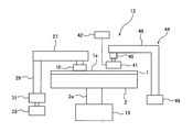
- FIG. 3 is a side view of the polishing apparatus shown in FIG.
- the surface texture measuring device 12 and the processing liquid supply nozzle 7 are not shown in FIG. 2, and the polishing head 5 and the processing liquid supply nozzle 7 are not shown in FIG.
- the polishing table 2 is connected to a table motor 15 through a table shaft 2a.
- the polishing table 2 and the polishing pad 1 are configured to be rotated by a table motor 15 around the axis.
- the upper surface of the polishing pad 1 constitutes the polishing surface 1 a for polishing the wafer W.
- the treatment liquid supply nozzle 7 is disposed above the polishing table 2 and the polishing pad 1 and is configured to selectively supply slurry or pure water onto the polishing surface 1 a of the polishing pad 1.
- the polishing head 5 is configured to hold the wafer W on its lower surface by vacuum suction or the like.
- the polishing head 5 is rotatably supported by the polishing head arm 18.
- the polishing head 5 is connected to a polishing head rotating mechanism (not shown) installed in the polishing head arm 18, and the polishing head 5 is rotated by the polishing head rotating mechanism about its axis. ing.
- the polishing head arm 18 is fixed to the polishing head turning shaft 19.
- the polishing head turning shaft 19 is connected to a polishing head turning mechanism 21 and a polishing head vertical movement mechanism 23.
- the polishing head vertical movement mechanism 23 is configured to be able to move the polishing head pivot shaft 19, the polishing head arm 18, and the polishing head 5 up and down together.
- the polishing head turning mechanism 21 is configured to rotate the polishing head turning shaft 19 clockwise and counterclockwise by a predetermined angle. When the polishing head turning mechanism 21 rotates the polishing head turning shaft 19, the polishing head arm 18 and the polishing head 5 turn in a plane parallel to the polishing surface 1a. More specifically, the polishing head 5 is movable between a polishing position above the polishing pad 1 and a wafer delivery position (substrate delivery position) outside the polishing pad 1.
- the dresser 10 is rotatably supported by the dresser arm 27.
- the dresser 10 is connected to a dresser rotation mechanism (not shown) installed in the dresser arm 27, and the dresser 10 is rotated by the dresser rotation mechanism about its axis.
- Abrasive grains such as diamond particles are fixed to the bottom of the dresser 10, and the abrasive grains constitute a dressing surface for dressing the polishing surface 1a.
- the dresser arm 27 is fixed to the dresser turning shaft 29.
- the dresser turning shaft 29 is connected to a dresser turning mechanism 31 and a dresser vertical movement mechanism 33.
- the dresser vertical movement mechanism 33 is configured to be able to move the dresser turning shaft 29, the dresser arm 27, and the dresser 10 up and down together.
- the dresser turning mechanism 31 is configured to rotate the dresser turning shaft 29 clockwise and counterclockwise by a predetermined angle. When the dresser turning mechanism 31 rotates the dresser turning shaft 29, the dresser arm 27 and the dresser 10 turn in a plane parallel to the polishing surface 1a. More specifically, the dresser 10 can reciprocate between the center region and the outer region of the polishing surface 1 a of the polishing pad 1.
- the wafer W is polished as follows.
- the polishing head 5 holds the wafer W on its lower surface and moves to a polishing position above the polishing surface 1 a of the polishing pad 1.
- the polishing head 5 is rotated by a polishing head rotating mechanism (not shown) about its axis.
- the polishing table 2 and the polishing pad 1 are rotated by a table motor 15, and slurry is further supplied from the processing liquid supply nozzle 7 onto the polishing surface 1 a of the polishing pad 1.
- the polishing head 5 presses the surface of the wafer W against the polishing surface 1 a of the polishing pad 1 while rotating around its axis.
- the surface of the wafer W is slidably contacted with the polishing pad 1 in the presence of the slurry, and is polished by the mechanical action of the abrasive grains contained in the slurry and the chemical action of the slurry.
- the dressing (or conditioning) of the polishing surface 1a of the polishing pad 1 is performed before and / or after the polishing of the wafer W.
- the dresser 10 is rotated around its axis by a dresser rotating mechanism (not shown), and the dressing surface (lower surface) of the dresser 10 is moved to the polishing surface 1 a of the polishing pad 1 by the dresser vertical movement mechanism 33. It is pressed against.
- the dresser 10 While supplying pure water from the treatment liquid supply nozzle 7 to the polishing surface 1 a of the polishing pad 1, the dresser 10 reciprocates on the polishing surface 1 a in the radial direction of the polishing pad 1 by the dresser turning mechanism 31.
- the dressing surface of the rotating dresser 10 regenerates the polishing surface 1 a by slightly scraping the polishing surface 1 a of the polishing pad 1.
- the dresser 10 may dress the polishing surface 1 a of the polishing pad 1 during polishing of the wafer W.
- the surface texture measuring device 12 of the polishing pad 1 includes a measuring head 41 and a data processing unit 42.
- the measuring head 41 is disposed above the polishing surface 1 a of the polishing pad 1.
- the measurement head 41 is connected to a parallel movement mechanism 44 that moves the measurement head 41 in a plane parallel to the polishing surface 1a and a vertical movement mechanism 45 that moves the measurement head 41 up and down.
- the translation mechanism 44 includes a support structure 48 that supports the measurement head 41, and a rotary actuator 49 that is coupled to the support structure 48.
- the rotary actuator 49 is disposed outside the polishing table 2.
- the rotary actuator 49 includes a combination of a motor and a torque transmission mechanism (for example, a reduction gear).
- the support structure 48 extends from the outside of the polishing table 2 to a position above the polishing table 2.
- the support structure 48 is not particularly limited as long as it has a rigid configuration such as an arm, a block, a truss structure, a rigid frame structure, or the like.
- One end of the support structure 48 is connected to the vertical movement mechanism 45, and the other end of the support structure 48 is connected to the rotary actuator 49.
- the vertical movement mechanism 45 is disposed above the polishing table 2 and the polishing pad 1, and the measurement head 41 is connected to and supported by the vertical movement mechanism 45.
- the vertical movement mechanism 45 may be composed of a combination of a servo motor and a ball screw mechanism.
- the vertical movement mechanism 45 may be connected to the rotary actuator 49 to move the rotary actuator 49, the support structure 48, and the measurement head 41 up and down together.
- the rotary actuator 49 is configured to rotate the support structure 48 clockwise and counterclockwise by a predetermined angle.
- the measuring head 41 moves above the polishing surface 1a of the polishing pad 1 in a direction parallel to the polishing surface 1a.
- the measurement head 41 moves in the radial direction of the polishing pad 1.
- the parallel movement mechanism 44 can move the measurement head 41 to a preset measurement position.
- the vertical movement mechanism 45 can raise or lower the measuring head 41 to a desired height.
- the measuring head 41 measures the property of the polishing surface 1a of the polishing pad 1 at the measurement position. Specific examples of the properties of the polished surface 1a include the surface shape.
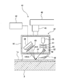
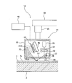
- FIG. 4 is a cross-sectional view of the measuring head 41.
- the measurement head 41 includes a casing 50 that does not transmit light including infrared rays, visible light, and ultraviolet rays, and an optical window 51 that is fixed to the bottom of the casing 50.
- the optical window 51 is made of a transparent material that allows light to pass therethrough.
- the optical window 51 constitutes the bottom of the measuring head 41 and faces the polishing surface 1 a of the polishing pad 1. Light can enter the internal space of the housing 50 only through the optical window 51.
- the housing 50 is connected to the parallel movement mechanism 44 and the vertical movement mechanism 45 described above.
- the measuring head 41 further includes a laser light source 55, an incident light mirror 57, and a light receiving sensor 59 arranged in the housing 50.
- the laser light source 55 is arranged facing the incident light mirror 57 and is configured to emit a laser beam toward the incident light mirror 57.
- the laser beam is reflected by the incident beam mirror 57 and guided to the polishing surface 1a of the polishing pad 1 through the optical window 51 which is a transparent window.
- the incident beam mirror 57 is configured to be rotatable about a rotation axis 58 so that the reflection angle of the laser beam can be changed.
- the laser beam is reflected and scattered by the polishing surface 1a to form scattered light. This scattered light travels toward the measuring head 41.
- the light receiving sensor 59 is configured to be able to measure the intensity of scattered light.
- the light receiving sensor 59 includes an image sensor such as a CCD sensor or a CMOS sensor.
- a polarizing filter 61 and a neutral density filter (ND filter) 62 are disposed between the laser light source 55 and the optical window 51.
- the polarizing filter 61 is an optical filter that passes only light that vibrates in a specific direction.
- the neutral density filter 62 is an optical filter that reduces light.
- the polarizing filter 61 and the neutral density filter 62 are disposed in the housing 50.
- the laser beam emitted from the laser light source 55 strikes the incident beam mirror 57 through the polarizing filter 61 and the neutral density filter 62. Accordingly, the weakened laser beam that vibrates in a specific direction is guided to the polishing surface 1 a of the polishing pad 1.
- the reason why the polarizing filter 61 is provided is as follows.
- the reflectance of the p-polarized component of the incident laser beam is lower than the reflectance of the s-polarized component. Further, the p-polarized component is easily transmitted through the polishing pad 1 or is easily absorbed by the polishing pad 1.
- the surface property measuring device 12 of this embodiment is desired to measure the property of the outermost layer of the polishing pad 1. If the incident laser beam contains a p-polarized component, more components are scattered by the holes in the polishing pad 1. As a result, the scattered light detected by the light receiving sensor 59 includes not only a component reflecting the surface property of the polishing pad 1 but also a scattering component generated inside the polishing pad 1 as a disturbance.
- a polarizing filter 61 is provided to remove the p-polarized component.
- the polarizing filter 61 is an optical filter that allows only a light component that vibrates in a direction perpendicular to an incident surface (a plane that includes an incident laser beam and is perpendicular to the polishing surface 1a of the polishing pad 1) to pass.
- the polishing pad 1 can be irradiated with a laser beam containing only the s-polarized component.
- the light receiving sensor 59 can detect the scattered light that does not include the scattering component generated inside the polishing pad 1.
- the reason why the neutral density filter 62 is provided is as follows.
- the light receiving sensor 59 has an upper limit of detectable light intensity. When the light receiving sensor 59 receives light having an intensity exceeding the upper limit, the intensity of the detected light is saturated, and the surface texture measuring device 12 cannot correctly measure the surface texture of the polishing pad 1. Therefore, by passing the laser beam through the neutral density filter 62, saturation of the light intensity at the light receiving sensor 59 can be prevented, and the surface texture measuring device 12 can correctly measure the surface texture of the polishing pad 1.
- the polarizing filter 61 and the neutral density filter 62 are disposed between the laser light source 55 and the incident light mirror 57. In one embodiment, one or both of the polarizing filter 61 and the neutral density filter 62 may be disposed between the incident light mirror 57 and the optical window 51.
- the measuring head 41 further includes a band pass filter 65 that covers the light receiving surface of the light receiving sensor 59.
- the band pass filter 65 is disposed in the housing 50 and is disposed between the optical window 51 and the light receiving sensor 59.
- the bandpass filter 65 is configured to pass only light having a wavelength within a limited range including the wavelength of the laser beam emitted from the laser light source 55.
- the bandpass filter 65 may be configured to pass only light having substantially the same wavelength as the laser beam.
- Such a bandpass filter 65 can remove light other than the laser beam, which can be a disturbance such as natural light.
- the measuring head 41 includes a jet nozzle 69 that sends a gas jet to the polishing surface 1 a of the polishing pad 1.
- the jet nozzle 69 is fixed to the bottom of the housing 50 and is close to the optical window 51.
- the jet nozzle 69 is inclined downward. Slurry and / or pure water can be removed from the polishing surface 1a by causing the gas jet 69 to collide with the polishing surface 1a. Examples of the gas used include clean air or an inert gas such as nitrogen gas.
- the measuring head 41 can irradiate the polishing surface 1a with a laser beam while removing slurry and / or pure water from the polishing surface 1a by a gas jet. Therefore, the surface texture measuring device 12 can accurately measure the surface texture of the polishing pad 1 without being affected by the slurry and / or pure water.
- the casing 50, the optical window 51, the laser light source 55, the incident light mirror 57, the light receiving sensor 59, the polarization filter 61, the neutral density filter 62, the band pass filter 65, and the jet nozzle 69 constituting the measurement head 41. Are moved together by a parallel movement mechanism 44 and moved up and down by a vertical movement mechanism 45.
- the light receiving sensor 59 of the measuring head 41 is connected to the data processing unit 42, and the measurement data acquired by the light receiving sensor 59 is sent to the data processing unit 42.
- the data processing unit 42 is configured to generate a spectrum of scattered light from the measurement data of the scattered light and calculate a pad surface index from the spectrum.
- the measurement data includes the light receiving position (that is, pixel position) of the light receiving sensor 59 and the intensity of scattered light at each light receiving position.
- the data processing unit 42 generates a spectrum of scattered light as shown in FIG. 5 from the measurement data.
- the vertical axis in FIG. 5 represents the intensity of the scattered light
- the horizontal axis represents the light receiving position of the light receiving sensor 59.
- the spectrum shown in FIG. 5 is a power spectrum showing the intensity distribution of scattered light.
- the spectrum of scattered light corresponds to a spectrum obtained by performing spatial Fourier transform (or spatial fast Fourier transform) on the surface shape of the polishing pad 1.
- the light receiving position of the light receiving sensor 59 shown on the horizontal axis shown in FIG. 5 corresponds to the spatial wavelength of the surface shape of the polishing pad 1.
- the data processing unit 42 performs a known process on the spectrum of scattered light shown in FIG. 5 to obtain a pad surface index.
- This known processing includes calculation of the integrated value of the scattered light intensity in the specific spatial wavelength region, or calculation of the ratio of the integrated value of the second spatial wavelength region to the integrated value of the first spatial wavelength region.
- the pad surface index indicates the surface property of the polishing surface 1 a of the polishing pad 1, that is, the polishing performance of the polishing pad 1.
- the light receiving sensor 59 In order to calculate the pad surface index that correctly indicates the polishing performance of the polishing pad 1, it is necessary for the light receiving sensor 59 to receive the scattered light reflected in an appropriate angle range. Specifically, the light receiving sensor 59 preferably receives scattered light from the 0th order light to the 7th order light. The integer order light appears on the spectrum as a characteristic peak as shown in FIG.
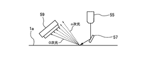
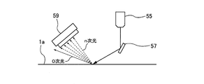
- the range of scattered light that can be received by the light receiving sensor 59 varies according to the height of the light receiving sensor 59 from the polishing surface 1 a of the polishing pad 1. For example, as shown in FIG. 6, when the light receiving sensor 59 is at a position that is too low, the light receiving sensor 59 cannot receive high-order light. On the other hand, as shown in FIG. 7, when the light receiving sensor 59 is at a position that is too high, the light receiving sensor 59 cannot receive low-order light.
- the light receiving sensor 59 shown in FIG. 4 can receive scattered light from 0th order light to higher order light. That is, there is an optimum height of the light receiving sensor 59 that allows the light receiving sensor 59 to receive scattered light from 0th order light to higher order light.
- the vertical movement mechanism 45 moves the entire measurement head 41 including the light receiving sensor 59 from the 0th order light of the scattered light to the position where the light receiving sensor 59 can receive the nth order light (n is a predetermined natural number). It is configured to raise and / or lower. More specifically, the laser light source 55 irradiates the polishing surface 1a of the polishing pad 1 with a laser beam, and the scattered light from the polishing surface 1a is detected by the light receiving sensor 59 while the light receiving sensor 59 determines a predetermined optimum light receiving position. In addition, the vertical movement mechanism 45 raises and / or lowers the measuring head 41 until the highest intensity scattered light (the 0th order light has the highest intensity) is incident.
- the optimum light receiving position is a position at which the light receiving sensor 59 can receive scattered light from the 0th order light to the nth order light when the highest intensity scattered light enters the optimum light receiving position.
- the light receiving sensor 59 can receive scattered light from the 0th order light to the higher order light.
- the vertical movement mechanism 45 may be arranged in the housing 50 and configured to raise and / or lower the light receiving sensor 59.
- FIG. 8 is a diagram showing another embodiment of the measurement head 41.
- a scattered light mirror 70 is disposed between the optical window 51 and the light receiving sensor 59.
- the scattered light mirror 70 is disposed in the housing 50.
- the scattered light from the polishing pad 1 passes through the optical window 51, is reflected by the scattered light mirror 70, and is guided to the light receiving sensor 59. According to such an arrangement, the degree of freedom of arrangement of the light receiving sensor 59 in the housing 50 is increased, and the measuring head 41 can be reduced in size.
- the scattered light mirror 70 may be a concave mirror.
- the scattered light mirror 70 made of a concave mirror can focus the scattered light. Therefore, a smaller light receiving sensor can be used as the light receiving sensor 59, which contributes to the downsizing of the measuring head 41.
- FIG. 9 is a view showing an embodiment in which the measurement head 41 is fixed to the dresser arm 27.
- the measuring head 41 moves with the dresser 10 above the polishing pad 1.
- the parallel movement mechanism for moving the measuring head 41 in a plane parallel to the polishing surface 1a is the dresser arm 27, the dresser turning shaft 29 (see FIG. 2), and the dresser turning mechanism 31 (see FIG. 2).
- the vertical movement mechanism configured to move the measurement head 41 up and down is constituted by a dresser vertical movement mechanism 33 (see FIG. 2).
- FIG. 10 is a view showing an embodiment in which the measurement head 41 is fixed to the polishing head arm 18.
- the measuring head 41 moves above the polishing pad 1 together with the polishing head 5.
- the parallel movement mechanism for moving the measuring head 41 in a plane parallel to the polishing surface 1a is the polishing head arm 18, the polishing head turning shaft 19 (see FIG. 2), and the polishing head turning mechanism 21 (FIG. 2).
- the vertical movement mechanism that moves the measurement head 41 up and down is constituted by the polishing head vertical movement mechanism 23 (see FIG. 2).
- the present invention can be used in a surface property measuring apparatus for a polishing pad that measures surface properties such as a surface shape and a surface state of a polishing pad used for polishing a substrate such as a semiconductor wafer.
Landscapes
- Engineering & Computer Science (AREA)
- Mechanical Engineering (AREA)
- Physics & Mathematics (AREA)
- General Physics & Mathematics (AREA)
- Mechanical Treatment Of Semiconductor (AREA)
- Finish Polishing, Edge Sharpening, And Grinding By Specific Grinding Devices (AREA)
- Constituent Portions Of Griding Lathes, Driving, Sensing And Control (AREA)
- Length Measuring Devices By Optical Means (AREA)
Abstract
本発明は、半導体ウェーハ等の基板の研磨に用いられる研磨パッドの表面形状や表面状態などの表面性状を測定する研磨パッドの表面性状測定装置に関するものである。表面性状測定装置は、光を通さない筐体(50)と、筐体(50)に取り付けられた光学窓(51)と、レーザー光線を発するレーザー光源(55)と、レーザー光線を光学窓(51)を通じて研磨パッド(1)に導く入射光線ミラー(57)と、レーザー光線が研磨パッド(1)に当たったときに発生する散乱光の強度を測定する受光センサー(59)とを備える。レーザー光源(55)、入射光線ミラー(57)、および受光センサー(59)は、筐体(50)内に配置されている。
Description
本発明は、半導体ウェーハ等の基板の研磨に用いられる研磨パッドの表面形状や表面状態などの表面性状を測定する研磨パッドの表面性状測定装置に関するものである。
近年、半導体デバイスの高集積化・高密度化に伴い、回路の配線がますます微細化し、多層配線の層数も増加している。回路の微細化を図りながら多層配線を実現しようとすると、下側の層の表面凹凸を踏襲しながら段差がより大きくなるので、配線層数が増加するに従って、薄膜形成における段差形状に対する膜被覆性(ステップカバレッジ)が悪くなる。したがって、多層配線するためには、このステップカバレッジを改善し、然るべき過程で平坦化処理しなければならない。また光リソグラフィの微細化とともに焦点深度が浅くなるため、半導体デバイスの表面の凹凸段差が焦点深度以下に収まるように半導体デバイス表面を平坦化処理する必要がある。
従って、半導体デバイスの製造工程においては、半導体デバイス表面の平坦化技術がますます重要になっている。この平坦化技術のうち、最も重要な技術は、化学的機械的研磨(CMP(Chemical Mechanical Polishing))である。この化学的機械的研磨は、研磨装置を用いて、シリカ(SiO2)やセリア(CeO2)等の砥粒を含んだ研磨液を研磨パッドに供給しつつ半導体ウェーハなどの基板を研磨パッドに摺接させて研磨を行うものである。
上述したCMPを行う研磨装置は、研磨パッドを有する研磨テーブルと、半導体ウェーハ(基板)を保持するためのキャリア又はトップリング等と称される基板保持装置とを備えている。このような研磨装置を用いて基板保持装置により基板を保持しつつ、この基板を研磨パッドに対して所定の圧力で押圧して、基板上の絶縁膜や金属膜を研磨することが行われている。
基板の研磨を行なうと、研磨パッドの表面には砥粒や研磨屑が付着し、また、研磨パッドの表面形状や状態が変化して研磨性能が劣化してくる。このため、基板の研磨を繰り返すに従い、研磨速度が低下し、また、研磨むらが生じてしまう。そこで、劣化した研磨パッドの表面形状や状態を再生するために、ドレッサーを用いて研磨パッドのドレッシング(コンディショニング)を行っている。
櫛田高志,木村景一,カチョーンルンルアン・パナート,鈴木恵友著「光学的フーリエ変換に基づくCMP用ポリシングパッドの表面形状評価に関する研究(第二報)―測定装置の試作―」2012年度精密工学会春季大会学術講演会講演論文集,2012年3月14日頒布,p.823-824
櫛田高志,木村景一,カチョーンルンルアン・パナート,鈴木恵友著「光学的フーリエ変換に基づいたCMP用ポリシングパッドの表面形上評価に関する研究」2011年度精密工学会秋季大会学術講演会講演論文集,2011年9月20日頒布,p.159-160
CMP(化学的機械的研磨)においては、研磨パッドの表面形状や状態は研磨性能に与える影響が大きく、種々の測定方法により研磨パッドの表面形状、状態を測定して、ドレッシング条件や研磨条件に反映させることが提案されている。
上記非特許文献1及び2には、研磨パッドの表面にレーザー光を照射し、その散乱反射光を光学的FFT解析することにより研磨パッドの表面形状特性を測定可能であることが示唆されている。
上記非特許文献1及び2には、研磨パッドの表面にレーザー光を照射し、その散乱反射光を光学的FFT解析することにより研磨パッドの表面形状特性を測定可能であることが示唆されている。
研磨パッドの表面にレーザー光を照射し、その散乱反射光を用いて研磨パッドの表面形状や表面状態などの表面性状を測定するにあたって、種々の外乱等の影響があるため、散乱反射光を適切にセンシングすることが重要である。
本発明は、上述の事情に鑑みなされたもので、種々の外乱等の影響を排除して研磨パッドの表面性状を正確に測定することができる研磨パッドの表面性状測定装置および当該測定装置を備えた研磨装置を提供することを目的とする。
上述した目的を達成するために、本発明の一態様は、基板の研磨に使用される研磨パッドの表面性状測定装置であって、光を通さない筐体と、前記筐体に取り付けられた光学窓と、レーザー光線を発するレーザー光源と、前記レーザー光線を前記光学窓を通じて前記研磨パッドに導く入射光線ミラーと、前記レーザー光線が前記研磨パッドに当たったときに発生する散乱光の強度を測定する受光センサーとを備え、前記レーザー光源、前記入射光線ミラー、および前記受光センサーは、前記筐体内に配置されていることを特徴とする。
本発明の好ましい態様は、前記受光センサーを上下動させる上下動機構をさらに備えたことを特徴とする。
本発明の好ましい態様は、前記上下動機構は、前記散乱光の0次光からn次光(nは予め定められた自然数)を前記受光センサーが受けることができる位置まで、前記受光センサーを上昇および/または下降させることを特徴とする。
本発明の好ましい態様は、前記研磨パッドの研磨面に気体の噴流を送る噴流ノズルをさらに備え、前記噴流ノズルは前記筐体に固定されていることを特徴とする。
本発明の好ましい態様は、前記光学窓と前記受光センサーとの間に配置されたバンドパスフィルターをさらに備えたことを特徴とする。
本発明の好ましい態様は、前記バンドパスフィルターは、前記レーザー光線の波長を含む限られた範囲内の波長を持つ光のみを通過させるように構成されていることを特徴とする。
本発明の好ましい態様は、前記上下動機構は、前記散乱光の0次光からn次光(nは予め定められた自然数)を前記受光センサーが受けることができる位置まで、前記受光センサーを上昇および/または下降させることを特徴とする。
本発明の好ましい態様は、前記研磨パッドの研磨面に気体の噴流を送る噴流ノズルをさらに備え、前記噴流ノズルは前記筐体に固定されていることを特徴とする。
本発明の好ましい態様は、前記光学窓と前記受光センサーとの間に配置されたバンドパスフィルターをさらに備えたことを特徴とする。
本発明の好ましい態様は、前記バンドパスフィルターは、前記レーザー光線の波長を含む限られた範囲内の波長を持つ光のみを通過させるように構成されていることを特徴とする。
本発明の好ましい態様は、前記レーザー光源と前記光学窓との間に配置された減光フィルターをさらに備えたことを特徴とする。
本発明の好ましい態様は、前記レーザー光源と前記光学窓との間に配置された偏光フィルターをさらに備えたことを特徴とする。
本発明の好ましい態様は、前記研磨パッドの研磨面に平行な平面内で前記筐体を移動させる平行移動機構をさらに備えたことを特徴とする。
本発明の好ましい態様は、前記研磨パッドからの散乱光を反射させ、前記受光センサーに導く散乱光ミラーをさらに備えたことを特徴とする。
本発明の好ましい態様は、前記散乱光ミラーは、凹面ミラーであることを特徴とする。
本発明の好ましい態様は、前記レーザー光源と前記光学窓との間に配置された偏光フィルターをさらに備えたことを特徴とする。
本発明の好ましい態様は、前記研磨パッドの研磨面に平行な平面内で前記筐体を移動させる平行移動機構をさらに備えたことを特徴とする。
本発明の好ましい態様は、前記研磨パッドからの散乱光を反射させ、前記受光センサーに導く散乱光ミラーをさらに備えたことを特徴とする。
本発明の好ましい態様は、前記散乱光ミラーは、凹面ミラーであることを特徴とする。
本発明の一態様は、研磨パッドを支持する研磨テーブルと、基板を前記研磨パッドに押し付ける研磨ヘッドと、前記研磨パッドの表面性状を測定する上記表面性状測定装置とを備えたことを特徴とする研磨装置である。
本発明によれば、筐体は、レーザー光源や受光センサーを含む光学系をスラリーや純水などの液体から保護することができるのみならず、レーザー光線以外の光を遮ることができる。したがって、表面性状測定装置は、種々の外乱等の影響を排除して研磨パッドの表面性状を正確に測定することができる。上下動機構は、受光センサーが0次光からn次光までの散乱光を受けることができる最適な位置にまで受光センサーを移動させることができる。したがって、表面性状測定装置は、研磨パッドの表面性状を正確に測定することができる。
以下、本発明の実施形態について図面を参照して説明する。
図1は、研磨パッドの表面性状測定装置を備えた研磨装置の一実施形態を示す模式平面図である。
研磨装置は、研磨面1aを有する研磨パッド1を支持する研磨テーブル2と、基板の一例であるウェーハWを研磨するための研磨ヘッド5と、研磨パッド1上にスラリーまたは純水を選択的に供給する処理液供給ノズル7と、研磨パッド1の研磨面1aをドレッシング(またはコンディショニング)するドレッサー10と、研磨パッド1の表面性状を測定する表面性状測定装置12とを備えている。
図1は、研磨パッドの表面性状測定装置を備えた研磨装置の一実施形態を示す模式平面図である。
研磨装置は、研磨面1aを有する研磨パッド1を支持する研磨テーブル2と、基板の一例であるウェーハWを研磨するための研磨ヘッド5と、研磨パッド1上にスラリーまたは純水を選択的に供給する処理液供給ノズル7と、研磨パッド1の研磨面1aをドレッシング(またはコンディショニング)するドレッサー10と、研磨パッド1の表面性状を測定する表面性状測定装置12とを備えている。
図2は、図1に示す研磨装置を矢印Aの方向から見た側面図であり、図3は、図1に示す研磨装置を矢印Bの方向から見た側面図である。説明のために、図2では、表面性状測定装置12および処理液供給ノズル7の図示は省略されており、図3では、研磨ヘッド5および処理液供給ノズル7の図示は省略されている。
研磨テーブル2はテーブル軸2aを介してテーブルモータ15に連結されている。研磨テーブル2および研磨パッド1はその軸心を中心にテーブルモータ15によって回転されるように構成されている。研磨パッド1の上面は、ウェーハWを研磨するための上記研磨面1aを構成している。処理液供給ノズル7は、研磨テーブル2および研磨パッド1の上方に配置されており、研磨パッド1の研磨面1a上にスラリーまたは純水を選択的に供給するように構成されている。
研磨ヘッド5は、その下面にウェーハWを真空吸引などにより保持することができるように構成されている。研磨ヘッド5は研磨ヘッドアーム18に回転可能に支持されている。研磨ヘッド5は、研磨ヘッドアーム18内に設置された研磨ヘッド回転機構(図示せず)に連結されており、研磨ヘッド5はその軸心を中心に研磨ヘッド回転機構によって回転されるようになっている。
研磨ヘッドアーム18は、研磨ヘッド旋回軸19に固定されている。この研磨ヘッド旋回軸19は、研磨ヘッド旋回機構21および研磨ヘッド上下動機構23に連結されている。研磨ヘッド上下動機構23は、研磨ヘッド旋回軸19、研磨ヘッドアーム18、および研磨ヘッド5を一体に上下動させることが可能に構成されている。研磨ヘッド旋回機構21は、研磨ヘッド旋回軸19を所定の角度だけ時計回りおよび反時計回りに回転させるように構成されている。研磨ヘッド旋回機構21が研磨ヘッド旋回軸19を回転させると、研磨ヘッドアーム18および研磨ヘッド5は、研磨面1aと平行な平面内で旋回する。より具体的には、研磨ヘッド5は、研磨パッド1の上方の研磨位置と、研磨パッド1の外側のウェーハ受け渡し位置(基板受け渡し位置)との間を移動可能となっている。
ドレッサー10はドレッサーアーム27に回転可能に支持されている。ドレッサー10は、ドレッサーアーム27内に設置されたドレッサー回転機構(図示せず)に連結されており、ドレッサー10はその軸心を中心にドレッサー回転機構によって回転されるようになっている。ドレッサー10の底部にはダイヤモンド粒子などの砥粒が固定されており、この砥粒は研磨面1aをドレッシングするためのドレッシング面を構成する。
ドレッサーアーム27は、ドレッサー旋回軸29に固定されている。このドレッサー旋回軸29は、ドレッサー旋回機構31およびドレッサー上下動機構33に連結されている。ドレッサー上下動機構33は、ドレッサー旋回軸29、ドレッサーアーム27、およびドレッサー10を一体に上下動させることが可能に構成されている。ドレッサー旋回機構31は、ドレッサー旋回軸29を所定の角度だけ時計回りおよび反時計回りに回転させるように構成されている。ドレッサー旋回機構31がドレッサー旋回軸29を回転させると、ドレッサーアーム27およびドレッサー10は、研磨面1aと平行な平面内で旋回する。より具体的には、ドレッサー10は、研磨パッド1の研磨面1aの中心側領域と外側領域との間を往復移動可能となっている。
ウェーハWは次のようにして研磨される。研磨ヘッド5はその下面にウェーハWを保持し、研磨パッド1の研磨面1aの上方の研磨位置に移動する。研磨ヘッド5は、その軸心を中心に研磨ヘッド回転機構(図示せず)により回転される。研磨テーブル2および研磨パッド1は、テーブルモータ15により回転され、さらに処理液供給ノズル7からスラリーが研磨パッド1の研磨面1a上に供給される。研磨ヘッド5は、その軸心を中心に回転しながら、ウェーハWの表面を研磨パッド1の研磨面1aに対して押し付ける。ウェーハWの表面は、スラリーの存在下で研磨パッド1に摺接され、スラリーに含まれる砥粒の機械的作用と、スラリーの化学的作用とにより研磨される。
ウェーハWの研磨前および/または研磨後に、研磨パッド1の研磨面1aのドレッシング(またはコンディショニング)が行われる。具体的には、ドレッサー10は、その軸心を中心にドレッサー回転機構(図示せず)により回転され、ドレッサー10のドレッシング面(下面)はドレッサー上下動機構33により研磨パッド1の研磨面1aに対して押し付けられる。純水を処理液供給ノズル7から研磨パッド1の研磨面1aに供給しながら、ドレッサー旋回機構31によりドレッサー10は研磨面1a上を研磨パッド1の半径方向に往復移動する。回転するドレッサー10のドレッシング面は、研磨パッド1の研磨面1aを僅かに削り取ることで、研磨面1aを再生する。一実施形態では、ドレッサー10は、ウェーハWの研磨中に研磨パッド1の研磨面1aをドレッシングしてもよい。
研磨パッド1の表面性状測定装置12は、測定ヘッド41とデータ処理部42を備えている。測定ヘッド41は、研磨パッド1の研磨面1aの上方に配置されている。測定ヘッド41は、研磨面1aに平行な平面内で測定ヘッド41を移動させる平行移動機構44、および測定ヘッド41を上下動させる上下動機構45に連結されている。平行移動機構44は、測定ヘッド41を支持する支持構造体48と、支持構造体48に連結された回転アクチュエータ49とを備えている。回転アクチュエータ49は、研磨テーブル2の外側に配置されている。回転アクチュエータ49は、モータおよびトルク伝達機構(例えば減速ギヤ)の組み合わせ等から構成される。
支持構造体48は、研磨テーブル2の外側から研磨テーブル2の上方位置まで延びている。支持構造体48は、アーム、ブロック、トラス構造、ラーメン構造などの剛性のある構成を有していれば、特に限定されない。支持構造体48の一端は上下動機構45に連結され、支持構造体48の他端は回転アクチュエータ49に連結されている。
本実施形態では、上下動機構45は、研磨テーブル2および研磨パッド1の上方に配置されており、測定ヘッド41は上下動機構45に連結され、かつ支持されている。上下動機構45は、サーボモータとボールねじ機構との組み合わせから構成されてもよい。一実施形態では、上下動機構45は、回転アクチュエータ49に接続され、回転アクチュエータ49、支持構造体48、および測定ヘッド41を一体に上下動させてもよい。
回転アクチュエータ49は、支持構造体48を所定の角度だけ時計回りおよび反時計回りに回転させるように構成されている。回転アクチュエータ49が支持構造体48を回転させると、測定ヘッド41は研磨パッド1の研磨面1aの上方を研磨面1aと平行な方向に移動する。本実施形態では、測定ヘッド41は、研磨パッド1の半径方向に移動する。平行移動機構44は、測定ヘッド41を予め設定された測定位置まで移動させることができる。上下動機構45は、測定ヘッド41を所望の高さにまで上昇または下降させることができる。測定ヘッド41は、上記測定位置において、研磨パッド1の研磨面1aの性状を測定する。研磨面1aの性状の具体例としては、表面形状が挙げられる。
図4は、測定ヘッド41の断面図である。測定ヘッド41は、赤外線、可視光線、紫外線を含む光を通さない筐体50と、筐体50の底部に固定された光学窓51を備えている。光学窓51は光の通過を許容する透明な材料から構成されている。光学窓51は、測定ヘッド41の底部を構成し、研磨パッド1の研磨面1aに対向している。光は、光学窓51のみを通じて筐体50の内部空間に入ることができる。筐体50は、上述した平行移動機構44および上下動機構45に連結されている。
測定ヘッド41は、筐体50内に配置されたレーザー光源55、入射光線ミラー57、および受光センサー59をさらに備えている。レーザー光源55は、入射光線ミラー57を向いて配置されており、レーザー光線を入射光線ミラー57に向けて発するように構成されている。レーザー光線は入射光線ミラー57で反射し、透明窓である光学窓51を通って研磨パッド1の研磨面1aに導かれる。入射光線ミラー57は、レーザー光線の反射角度を変えることができるように、回転軸58を中心に回転可能に構成されている。レーザー光線は、研磨面1aで反射および散乱し、散乱光を形成する。この散乱光は、測定ヘッド41に向かって進む。
研磨パッド1の研磨面1aからの散乱光は、光学窓51を通過し、受光センサー59によって検出される。受光センサー59は、散乱光の強度を測定することができるように構成されている。受光センサー59は、CCDセンサー、CMOSセンサーなどのイメージセンサーから構成されている。
本実施形態では、レーザー光源55と光学窓51との間に、偏光フィルター61および減光フィルター(neutral-density filter またはNDフィルター)62が配置されている。偏光フィルター61は、ある特定の方向に振動する光のみを通過させる光学フィルターである。減光フィルター62は、光を減じる光学フィルターである。偏光フィルター61および減光フィルター62は、筐体50内に配置されている。レーザー光源55から発せられたレーザー光線は、偏光フィルター61および減光フィルター62を通って入射光線ミラー57に当たる。したがって、ある特定の方向に振動した、弱められたレーザー光線が研磨パッド1の研磨面1aに導かれる。
偏光フィルター61を設ける理由は、次の通りである。入射するレーザー光線のp偏光成分の反射率は、s偏光成分の反射率よりも低い。さらに、p偏光成分は研磨パッド1を透過しやすく、または研磨パッド1に吸収されやすい。本実施形態の表面性状測定装置12には、研磨パッド1の最表層の性状を測定することが望まれる。入射するレーザー光線がp偏光成分を含むと、研磨パッド1の内部の空孔で散乱する成分が多くなる。その結果、受光センサー59で検出される散乱光には、研磨パッドの1の表面性状を反映した成分のみならず、研磨パッド1の内部で発生した散乱成分が外乱として含まれてしまう。
そこで、本実施形態では、p偏光成分を除去するために、偏光フィルター61が設けられている。この偏光フィルター61は、入射面(入射するレーザー光線を含み、かつ研磨パッド1の研磨面1aに垂直な平面)に垂直な方向に振動する光成分のみを通過させる光学フィルターである。レーザー光線を偏光フィルター61に通すことで、s偏光成分のみを含むレーザー光線を研磨パッド1に照射することができる。結果として、受光センサー59は、研磨パッド1の内部で発生した散乱成分を含まない散乱光を検出することができる。
減光フィルター62を設ける理由は、次の通りである。受光センサー59には、検出可能な光の強度の上限が存在する。上限を超えた強度の光を受光センサー59が受光すると、検出された光の強度は飽和してしまい、表面性状測定装置12は研磨パッド1の表面性状を正しく測定できない。そこで、レーザー光線を減光フィルター62に通すことで、受光センサー59での光の強度の飽和を防止することができ、表面性状測定装置12は研磨パッド1の表面性状を正しく測定することができる。
本実施形態では、偏光フィルター61および減光フィルター62は、レーザー光源55と入射光線ミラー57との間に配置されている。一実施形態では、偏光フィルター61および減光フィルター62の一方または両方は、入射光線ミラー57と光学窓51との間に配置されてもよい。
本実施形態では、測定ヘッド41は、受光センサー59の受光面を覆うバンドパスフィルター65をさらに備えている。このバンドパスフィルター65は、筐体50内に配置されており、光学窓51と受光センサー59との間に配置されている。バンドパスフィルター65は、レーザー光源55から発せられたレーザー光線の波長を含む限られた範囲内の波長の光のみを通過させるように構成されている。一実施形態では、バンドパスフィルター65は、レーザー光線と実質的に同じ波長の光のみを通過させるように構成されてもよい。このようなバンドパスフィルター65は、自然光などの外乱となりうる、レーザー光線以外の光を除去することができる。
測定ヘッド41は、研磨パッド1の研磨面1aに気体の噴流を送る噴流ノズル69を備えている。この噴流ノズル69は、筐体50の底部に固定されており、光学窓51に近接している。噴流ノズル69は、下方に傾いている。噴流ノズル69が気体の噴流を研磨面1aに衝突させることで、スラリーおよび/または純水を研磨面1aから除去することができる。使用される気体の例としては、清浄な空気、または窒素ガスなどの不活性ガスが挙げられる。本実施形態によれば、測定ヘッド41は、気体の噴流によってスラリーおよび/または純水を研磨面1aから除去しながら、レーザー光線を研磨面1aに照射することができる。したがって、表面性状測定装置12は、スラリーおよび/または純水の影響を受けることなく、研磨パッド1の表面性状を正確に測定することができる。
本実施形態では、測定ヘッド41を構成する筐体50、光学窓51、レーザー光源55、入射光線ミラー57、受光センサー59、偏光フィルター61、減光フィルター62、バンドパスフィルター65、および噴流ノズル69は、平行移動機構44によって一体に移動され、上下動機構45によって一体に上下動される。
測定ヘッド41の受光センサー59は、データ処理部42に接続されており、受光センサー59によって取得された測定データはデータ処理部42に送られるようになっている。データ処理部42は、散乱光の測定データから散乱光のスペクトルを生成し、該スペクトルからパッド表面指数を算出するように構成される。測定データには、受光センサー59の受光位置(すなわち、ピクセル位置)、および各受光位置での散乱光の強度が含まれる。データ処理部42は、測定データから、図5に示すような、散乱光のスペクトルを生成する。図5の縦軸は、散乱光の強度を表し、横軸は、受光センサー59の受光位置を表している。図5に示すスペクトルは、散乱光の強度分布を示すパワースペクトルである。
上記非特許文献1,2に記載されているように、散乱光のスペクトルは、研磨パッド1の表面形状に対して空間的フーリエ変換(あるいは空間的高速フーリエ変換)を行って得られるスペクトルに相当する。図5に示す横軸に示される受光センサー59の受光位置は、研磨パッド1の表面形状の空間波長に相当する。
データ処理部42は、図5に示す散乱光のスペクトルに公知の処理を行って、パッド表面指数を求める。この公知の処理は、特定空間波長領域の散乱光強度の積分値の算出、または第一の空間波長領域の積分値に対する、第二の空間波長領域の積分値の比の算出などである。パッド表面指数は、研磨パッド1の研磨面1aの表面性状、すなわち研磨パッド1の研磨性能を示している。
研磨パッド1の研磨性能を正しく示すパッド表面指数を算出するためには、適切な角度範囲で反射した散乱光を受光センサー59が受ける必要がある。具体的には、受光センサー59は、0次光から7次光前後の散乱光を受けることが好ましい。整数次光は、図5に示すように、特徴的なピークとしてスペクトル上に現れる。
受光センサー59が受けることができる散乱光の範囲は、研磨パッド1の研磨面1aからの受光センサー59の高さに従って変わる。例えば、図6に示すように、受光センサー59が低すぎる位置にある場合、受光センサー59は高次光を受けることができない。一方、図7に示すように、受光センサー59が高すぎる位置にある場合、受光センサー59は低次光を受けることができない。図4に示す受光センサー59は、0次光から高次光までの散乱光を受けることができる。つまり、受光センサー59が0次光から高次光までの散乱光を受けることができる受光センサー59の最適な高さが存在する。
そこで、上下動機構45は、散乱光の0次光からn次光(nは予め定められた自然数)を受光センサー59が受けることができる位置まで、受光センサー59を含む測定ヘッド41の全体を上昇および/または下降させるように構成されている。より具体的には、レーザー光源55から研磨パッド1の研磨面1aにレーザー光線を照射し、研磨面1aからの散乱光を受光センサー59で検出しながら、受光センサー59の予め定められた最適受光位置に、最高強度の散乱光(0次光が最高強度を有する)が入射するまで、上下動機構45は測定ヘッド41を上昇および/または下降させる。上記最適受光位置は、最高強度の散乱光が最適受光位置に入射するときに、受光センサー59が0次光からn次光までの散乱光を受けることができる位置である。
このように研磨面1aからの受光センサー59の高さを調整することによって、受光センサー59は、0次光から高次光までの散乱光を受けることができる。一実施形態では、上下動機構45は、筐体50内に配置され、受光センサー59を上昇および/または下降させるように構成されてもよい。
図8は、測定ヘッド41の他の実施形態を示す図である。特に説明しない本実施形態の構成は、上述した実施形態と同じであるので、その重複する説明を省略する。この実施形態では、光学窓51と受光センサー59との間に散乱光ミラー70が配置されている。この散乱光ミラー70は、筐体50内に配置されている。研磨パッド1からの散乱光は、光学窓51を通過した後、散乱光ミラー70で反射し、受光センサー59に導かれる。このような配置によれば、筐体50内における受光センサー59の配置の自由度が増し、測定ヘッド41を小型化することができる。
一実施形態では、上記散乱光ミラー70は、凹面ミラーであってもよい。凹面ミラーからなる散乱光ミラー70は、散乱光を集束させることができる。したがって、受光センサー59として、より小型の受光センサーを使用することができ、測定ヘッド41の小型化に寄与する。
図9は、測定ヘッド41をドレッサーアーム27に固定した実施形態を示す図である。測定ヘッド41は、ドレッサー10とともに研磨パッド1の上方を移動する。この実施形態では、測定ヘッド41を研磨面1aと平行な平面内で移動させる平行移動機構は、ドレッサーアーム27、ドレッサー旋回軸29(図2参照)、およびドレッサー旋回機構31(図2参照)により構成され、測定ヘッド41を上下動させる上下動機構は、ドレッサー上下動機構33(図2参照)により構成される。
図10は、測定ヘッド41を研磨ヘッドアーム18に固定した実施形態を示す図である。測定ヘッド41は、研磨ヘッド5ともに研磨パッド1の上方を移動する。この実施形態では、測定ヘッド41を研磨面1aと平行な平面内で移動させる平行移動機構は、研磨ヘッドアーム18、研磨ヘッド旋回軸19(図2参照)、および研磨ヘッド旋回機構21(図2参照)により構成され、測定ヘッド41を上下動させる上下動機構は、研磨ヘッド上下動機構23(図2参照)により構成される。
上述した実施形態は、本発明が属する技術分野における通常の知識を有する者が本発明を実施できることを目的として記載されたものである。上記実施形態の種々の変形例は、当業者であれば当然になしうることであり、本発明の技術的思想は他の実施形態にも適用しうる。したがって、本発明は、記載された実施形態に限定されることはなく、特許請求の範囲によって定義される技術的思想に従った最も広い範囲に解釈されるものである。
本発明は、半導体ウェーハ等の基板の研磨に用いられる研磨パッドの表面形状や表面状態などの表面性状を測定する研磨パッドの表面性状測定装置に利用可能である。
1a 研磨面
1 研磨パッド
2 研磨テーブル
5 研磨ヘッド
7 処理液供給ノズル
10 ドレッサー
12 表面性状測定装置
15 テーブルモータ
18 研磨ヘッドアーム
19 研磨ヘッド旋回軸
21 研磨ヘッド旋回機構
23 研磨ヘッド上下動機構
27 ドレッサーアーム
29 ドレッサー旋回軸
31 ドレッサー旋回機構
33 ドレッサー上下動機構
41 測定ヘッド
42 データ処理部
44 平行移動機構
45 上下動機構
48 支持構造体
49 回転アクチュエータ
50 筐体
51 光学窓
55 レーザー光源
57 入射光線ミラー
58 回転軸
59 受光センサー
61 偏光フィルター
62 減光フィルター
65 バンドパスフィルター
70 散乱光ミラー
1 研磨パッド
2 研磨テーブル
5 研磨ヘッド
7 処理液供給ノズル
10 ドレッサー
12 表面性状測定装置
15 テーブルモータ
18 研磨ヘッドアーム
19 研磨ヘッド旋回軸
21 研磨ヘッド旋回機構
23 研磨ヘッド上下動機構
27 ドレッサーアーム
29 ドレッサー旋回軸
31 ドレッサー旋回機構
33 ドレッサー上下動機構
41 測定ヘッド
42 データ処理部
44 平行移動機構
45 上下動機構
48 支持構造体
49 回転アクチュエータ
50 筐体
51 光学窓
55 レーザー光源
57 入射光線ミラー
58 回転軸
59 受光センサー
61 偏光フィルター
62 減光フィルター
65 バンドパスフィルター
70 散乱光ミラー
Claims (12)
- 基板の研磨に使用される研磨パッドの表面性状測定装置であって、
光を通さない筐体と、
前記筐体に取り付けられた光学窓と、
レーザー光線を発するレーザー光源と、
前記レーザー光線を前記光学窓を通じて前記研磨パッドに導く入射光線ミラーと、
前記レーザー光線が前記研磨パッドに当たったときに発生する散乱光の強度を測定する受光センサーとを備え、
前記レーザー光源、前記入射光線ミラー、および前記受光センサーは、前記筐体内に配置されていることを特徴とする表面性状測定装置。 - 前記受光センサーを上下動させる上下動機構をさらに備えたことを特徴とする請求項1に記載の表面性状測定装置。
- 前記上下動機構は、前記散乱光の0次光からn次光(nは予め定められた自然数)を前記受光センサーが受けることができる位置まで、前記受光センサーを上昇および/または下降させることを特徴とする請求項2に記載の表面性状測定装置。
- 前記研磨パッドの研磨面に気体の噴流を送る噴流ノズルをさらに備え、前記噴流ノズルは前記筐体に固定されていることを特徴とする請求項1に記載の表面性状測定装置。
- 前記光学窓と前記受光センサーとの間に配置されたバンドパスフィルターをさらに備えたことを特徴とする請求項1に記載の表面性状測定装置。
- 前記バンドパスフィルターは、前記レーザー光線の波長を含む限られた範囲内の波長を持つ光のみを通過させるように構成されていることを特徴とする請求項5に記載の表面性状測定装置。
- 前記レーザー光源と前記光学窓との間に配置された減光フィルターをさらに備えたことを特徴とする請求項1に記載の表面性状測定装置。
- 前記レーザー光源と前記光学窓との間に配置された偏光フィルターをさらに備えたことを特徴とする請求項1に記載の表面性状測定装置。
- 前記研磨パッドの研磨面に平行な平面内で前記筐体を移動させる平行移動機構をさらに備えたことを特徴とする請求項1に記載の表面性状測定装置。
- 前記研磨パッドからの散乱光を反射させ、前記受光センサーに導く散乱光ミラーをさらに備えたことを特徴とする請求項1に記載の表面性状測定装置。
- 前記散乱光ミラーは、凹面ミラーであることを特徴とする請求項10に記載の表面性状測定装置。
- 研磨パッドを支持する研磨テーブルと、
基板を前記研磨パッドに押し付ける研磨ヘッドと、
前記研磨パッドの表面性状を測定する、請求項1乃至11のいずれか一項に記載の表面性状測定装置とを備えたことを特徴とする研磨装置。
Applications Claiming Priority (2)
| Application Number | Priority Date | Filing Date | Title |
|---|---|---|---|
| JP2016-204438 | 2016-10-18 | ||
| JP2016204438A JP2018065209A (ja) | 2016-10-18 | 2016-10-18 | 研磨パッドの表面性状測定装置 |
Publications (1)
| Publication Number | Publication Date |
|---|---|
| WO2018074041A1 true WO2018074041A1 (ja) | 2018-04-26 |
Family
ID=62019473
Family Applications (1)
| Application Number | Title | Priority Date | Filing Date |
|---|---|---|---|
| PCT/JP2017/029154 Ceased WO2018074041A1 (ja) | 2016-10-18 | 2017-08-10 | 研磨パッドの表面性状測定装置 |
Country Status (2)
| Country | Link |
|---|---|
| JP (1) | JP2018065209A (ja) |
| WO (1) | WO2018074041A1 (ja) |
Cited By (1)
| Publication number | Priority date | Publication date | Assignee | Title |
|---|---|---|---|---|
| CN110617786A (zh) * | 2018-06-18 | 2019-12-27 | 凯斯科技股份有限公司 | 垫监测装置及包括其的垫监测系统、垫监测方法 |
Families Citing this family (3)
| Publication number | Priority date | Publication date | Assignee | Title |
|---|---|---|---|---|
| TWI856837B (zh) * | 2019-03-21 | 2024-09-21 | 美商應用材料股份有限公司 | 監視化學機械拋光中的拋光墊紋理 |
| CN113070809B (zh) * | 2019-12-17 | 2022-07-05 | 大量科技股份有限公司 | 化学机械研磨装置的研磨垫检测方法与研磨垫检测装置 |
| CN117597215A (zh) * | 2021-07-06 | 2024-02-23 | 应用材料公司 | 使用光学传感器的化学机械抛光振动测量 |
Citations (10)
| Publication number | Priority date | Publication date | Assignee | Title |
|---|---|---|---|---|
| JP2000271854A (ja) * | 1999-03-25 | 2000-10-03 | Hitachi Ltd | 加工方法及びその装置並びに半導体基板の加工方法 |
| JP2001223190A (ja) * | 2000-02-08 | 2001-08-17 | Hitachi Ltd | 研磨パッドの表面状態評価方法及びその装置とそれを用いた薄膜デバイスの製造方法及びその製造装置 |
| JP2002261059A (ja) * | 2001-03-01 | 2002-09-13 | Omron Corp | 研磨状態検出装置 |
| JP2010120130A (ja) * | 2008-11-20 | 2010-06-03 | Disco Abrasive Syst Ltd | 研磨装置、研磨方法および研磨用制御プログラム |
| JP2012135857A (ja) * | 2010-12-28 | 2012-07-19 | Sumco Corp | 研削装置および両面研磨装置 |
| JP2013102223A (ja) * | 2004-05-14 | 2013-05-23 | Kla-Encor Corp | 試験体の測定または分析のためのシステムおよび方法 |
| JP2014132275A (ja) * | 2003-07-23 | 2014-07-17 | Kla-Encor Corp | 表面検査装置および表面検査方法 |
| JP2014172154A (ja) * | 2013-03-12 | 2014-09-22 | Ebara Corp | 研磨パッドの表面性状測定装置 |
| JP2015208840A (ja) * | 2014-04-30 | 2015-11-24 | 株式会社荏原製作所 | 研磨装置、研磨パッドプロファイル計測用治具、及び、研磨パッドプロファイル計測方法 |
| WO2016111335A1 (ja) * | 2015-01-07 | 2016-07-14 | 株式会社 荏原製作所 | 研磨パッドの表面性状測定装置を備えたcmp装置 |
-
2016
- 2016-10-18 JP JP2016204438A patent/JP2018065209A/ja active Pending
-
2017
- 2017-08-10 WO PCT/JP2017/029154 patent/WO2018074041A1/ja not_active Ceased
Patent Citations (10)
| Publication number | Priority date | Publication date | Assignee | Title |
|---|---|---|---|---|
| JP2000271854A (ja) * | 1999-03-25 | 2000-10-03 | Hitachi Ltd | 加工方法及びその装置並びに半導体基板の加工方法 |
| JP2001223190A (ja) * | 2000-02-08 | 2001-08-17 | Hitachi Ltd | 研磨パッドの表面状態評価方法及びその装置とそれを用いた薄膜デバイスの製造方法及びその製造装置 |
| JP2002261059A (ja) * | 2001-03-01 | 2002-09-13 | Omron Corp | 研磨状態検出装置 |
| JP2014132275A (ja) * | 2003-07-23 | 2014-07-17 | Kla-Encor Corp | 表面検査装置および表面検査方法 |
| JP2013102223A (ja) * | 2004-05-14 | 2013-05-23 | Kla-Encor Corp | 試験体の測定または分析のためのシステムおよび方法 |
| JP2010120130A (ja) * | 2008-11-20 | 2010-06-03 | Disco Abrasive Syst Ltd | 研磨装置、研磨方法および研磨用制御プログラム |
| JP2012135857A (ja) * | 2010-12-28 | 2012-07-19 | Sumco Corp | 研削装置および両面研磨装置 |
| JP2014172154A (ja) * | 2013-03-12 | 2014-09-22 | Ebara Corp | 研磨パッドの表面性状測定装置 |
| JP2015208840A (ja) * | 2014-04-30 | 2015-11-24 | 株式会社荏原製作所 | 研磨装置、研磨パッドプロファイル計測用治具、及び、研磨パッドプロファイル計測方法 |
| WO2016111335A1 (ja) * | 2015-01-07 | 2016-07-14 | 株式会社 荏原製作所 | 研磨パッドの表面性状測定装置を備えたcmp装置 |
Cited By (1)
| Publication number | Priority date | Publication date | Assignee | Title |
|---|---|---|---|---|
| CN110617786A (zh) * | 2018-06-18 | 2019-12-27 | 凯斯科技股份有限公司 | 垫监测装置及包括其的垫监测系统、垫监测方法 |
Also Published As
| Publication number | Publication date |
|---|---|
| JP2018065209A (ja) | 2018-04-26 |
Similar Documents
| Publication | Publication Date | Title |
|---|---|---|
| CN105738320B (zh) | 研磨垫的表面性状测定方法和装置 | |
| JP6025055B2 (ja) | 研磨パッドの表面性状測定方法 | |
| KR101930966B1 (ko) | 연마 패드의 표면 성상 측정 장치 | |
| WO2018074041A1 (ja) | 研磨パッドの表面性状測定装置 | |
| JP6622720B2 (ja) | 研磨パッドの表面性状測定装置を備えたcmp装置 | |
| TW202313252A (zh) | 研磨方法 | |
| JP6372847B2 (ja) | 研磨装置 | |
| WO2020144911A1 (ja) | 研磨装置 | |
| US20240075579A1 (en) | Surface property measuring apparatus for polishing pad, surface property measuring method for polishing pad, and surface property judging method for polishing pad | |
| TW202201513A (zh) | 研磨方法、研磨裝置、及記錄有程式之電腦可讀取記錄媒體 | |
| JP5037974B2 (ja) | 研磨加工ステージにおける半導体基板の監視機器および監視方法 | |
| JP2009088073A (ja) | 研削ステージでの半導体基板の厚み測定方法 | |
| JP2003285257A (ja) | 研磨パッド、研磨装置および半導体の製造方法 | |
| TW202426139A (zh) | 研磨裝置 |
Legal Events
| Date | Code | Title | Description |
|---|---|---|---|
| 121 | Ep: the epo has been informed by wipo that ep was designated in this application |
Ref document number: 17862214 Country of ref document: EP Kind code of ref document: A1 |
|
| NENP | Non-entry into the national phase |
Ref country code: DE |
|
| 122 | Ep: pct application non-entry in european phase |
Ref document number: 17862214 Country of ref document: EP Kind code of ref document: A1 |