WO2018061966A1 - Solar cell, solar cell module, and method for manufacturing solar cell - Google Patents
Solar cell, solar cell module, and method for manufacturing solar cell Download PDFInfo
- Publication number
- WO2018061966A1 WO2018061966A1 PCT/JP2017/034056 JP2017034056W WO2018061966A1 WO 2018061966 A1 WO2018061966 A1 WO 2018061966A1 JP 2017034056 W JP2017034056 W JP 2017034056W WO 2018061966 A1 WO2018061966 A1 WO 2018061966A1
- Authority
- WO
- WIPO (PCT)
- Prior art keywords
- layer
- amorphous
- amorphous silicon
- epitaxial
- silicon substrate
- Prior art date
Links
- 238000000034 method Methods 0.000 title claims description 40
- 238000004519 manufacturing process Methods 0.000 title claims description 17
- 239000000758 substrate Substances 0.000 claims abstract description 143
- XUIMIQQOPSSXEZ-UHFFFAOYSA-N Silicon Chemical compound [Si] XUIMIQQOPSSXEZ-UHFFFAOYSA-N 0.000 claims abstract description 112
- 229910052710 silicon Inorganic materials 0.000 claims abstract description 112
- 239000010703 silicon Substances 0.000 claims abstract description 112
- 229910021417 amorphous silicon Inorganic materials 0.000 claims description 260
- 230000015572 biosynthetic process Effects 0.000 claims description 151
- 239000013078 crystal Substances 0.000 claims description 59
- 239000002994 raw material Substances 0.000 claims description 4
- 238000001947 vapour-phase growth Methods 0.000 claims description 3
- 229910021419 crystalline silicon Inorganic materials 0.000 abstract description 11
- 238000002161 passivation Methods 0.000 description 190
- 238000011049 filling Methods 0.000 description 26
- 238000000151 deposition Methods 0.000 description 23
- 230000008021 deposition Effects 0.000 description 23
- 239000000463 material Substances 0.000 description 23
- 239000007789 gas Substances 0.000 description 20
- 229920005989 resin Polymers 0.000 description 14
- 239000011347 resin Substances 0.000 description 14
- 229910021421 monocrystalline silicon Inorganic materials 0.000 description 13
- KRHYYFGTRYWZRS-UHFFFAOYSA-N Fluorane Chemical compound F KRHYYFGTRYWZRS-UHFFFAOYSA-N 0.000 description 12
- 230000007423 decrease Effects 0.000 description 11
- 238000010586 diagram Methods 0.000 description 9
- UFHFLCQGNIYNRP-UHFFFAOYSA-N Hydrogen Chemical compound [H][H] UFHFLCQGNIYNRP-UHFFFAOYSA-N 0.000 description 7
- MHAJPDPJQMAIIY-UHFFFAOYSA-N Hydrogen peroxide Chemical compound OO MHAJPDPJQMAIIY-UHFFFAOYSA-N 0.000 description 7
- 239000001257 hydrogen Substances 0.000 description 7
- 229910052739 hydrogen Inorganic materials 0.000 description 7
- 238000000623 plasma-assisted chemical vapour deposition Methods 0.000 description 7
- BQCADISMDOOEFD-UHFFFAOYSA-N Silver Chemical compound [Ag] BQCADISMDOOEFD-UHFFFAOYSA-N 0.000 description 6
- HEMHJVSKTPXQMS-UHFFFAOYSA-M Sodium hydroxide Chemical compound [OH-].[Na+] HEMHJVSKTPXQMS-UHFFFAOYSA-M 0.000 description 6
- 238000006243 chemical reaction Methods 0.000 description 6
- 239000011521 glass Substances 0.000 description 6
- 229910052751 metal Inorganic materials 0.000 description 6
- 239000002184 metal Substances 0.000 description 6
- 239000011259 mixed solution Substances 0.000 description 6
- 238000005268 plasma chemical vapour deposition Methods 0.000 description 6
- 239000000853 adhesive Substances 0.000 description 5
- 230000001070 adhesive effect Effects 0.000 description 5
- 238000010248 power generation Methods 0.000 description 5
- 229910052709 silver Inorganic materials 0.000 description 5
- 239000004332 silver Substances 0.000 description 5
- 239000007864 aqueous solution Substances 0.000 description 4
- 239000000969 carrier Substances 0.000 description 4
- 238000005530 etching Methods 0.000 description 4
- 238000004050 hot filament vapor deposition Methods 0.000 description 4
- 238000010030 laminating Methods 0.000 description 4
- 239000011159 matrix material Substances 0.000 description 4
- 238000004544 sputter deposition Methods 0.000 description 4
- WGTYBPLFGIVFAS-UHFFFAOYSA-M tetramethylammonium hydroxide Chemical compound [OH-].C[N+](C)(C)C WGTYBPLFGIVFAS-UHFFFAOYSA-M 0.000 description 4
- QTBSBXVTEAMEQO-UHFFFAOYSA-N Acetic acid Chemical compound CC(O)=O QTBSBXVTEAMEQO-UHFFFAOYSA-N 0.000 description 3
- BLRPTPMANUNPDV-UHFFFAOYSA-N Silane Chemical compound [SiH4] BLRPTPMANUNPDV-UHFFFAOYSA-N 0.000 description 3
- 229910052782 aluminium Inorganic materials 0.000 description 3
- XAGFODPZIPBFFR-UHFFFAOYSA-N aluminium Chemical compound [Al] XAGFODPZIPBFFR-UHFFFAOYSA-N 0.000 description 3
- 239000000470 constituent Substances 0.000 description 3
- 238000007865 diluting Methods 0.000 description 3
- 239000005038 ethylene vinyl acetate Substances 0.000 description 3
- 238000003475 lamination Methods 0.000 description 3
- 239000002245 particle Substances 0.000 description 3
- 229910000077 silane Inorganic materials 0.000 description 3
- 239000000243 solution Substances 0.000 description 3
- GRYLNZFGIOXLOG-UHFFFAOYSA-N Nitric acid Chemical compound O[N+]([O-])=O GRYLNZFGIOXLOG-UHFFFAOYSA-N 0.000 description 2
- 239000011230 binding agent Substances 0.000 description 2
- DQXBYHZEEUGOBF-UHFFFAOYSA-N but-3-enoic acid;ethene Chemical compound C=C.OC(=O)CC=C DQXBYHZEEUGOBF-UHFFFAOYSA-N 0.000 description 2
- ZOCHARZZJNPSEU-UHFFFAOYSA-N diboron Chemical compound B#B ZOCHARZZJNPSEU-UHFFFAOYSA-N 0.000 description 2
- 239000002019 doping agent Substances 0.000 description 2
- 230000000694 effects Effects 0.000 description 2
- 239000011888 foil Substances 0.000 description 2
- AMGQUBHHOARCQH-UHFFFAOYSA-N indium;oxotin Chemical compound [In].[Sn]=O AMGQUBHHOARCQH-UHFFFAOYSA-N 0.000 description 2
- 239000012528 membrane Substances 0.000 description 2
- 229910017604 nitric acid Inorganic materials 0.000 description 2
- 229920001200 poly(ethylene-vinyl acetate) Polymers 0.000 description 2
- 229910021420 polycrystalline silicon Inorganic materials 0.000 description 2
- 229920000139 polyethylene terephthalate Polymers 0.000 description 2
- 239000005020 polyethylene terephthalate Substances 0.000 description 2
- 229920000098 polyolefin Polymers 0.000 description 2
- 238000007650 screen-printing Methods 0.000 description 2
- 239000004065 semiconductor Substances 0.000 description 2
- 229910000679 solder Inorganic materials 0.000 description 2
- 238000007740 vapor deposition Methods 0.000 description 2
- RYGMFSIKBFXOCR-UHFFFAOYSA-N Copper Chemical compound [Cu] RYGMFSIKBFXOCR-UHFFFAOYSA-N 0.000 description 1
- XYFCBTPGUUZFHI-UHFFFAOYSA-N Phosphine Chemical compound P XYFCBTPGUUZFHI-UHFFFAOYSA-N 0.000 description 1
- KWYUFKZDYYNOTN-UHFFFAOYSA-M Potassium hydroxide Chemical compound [OH-].[K+] KWYUFKZDYYNOTN-UHFFFAOYSA-M 0.000 description 1
- 229910052581 Si3N4 Inorganic materials 0.000 description 1
- VYPSYNLAJGMNEJ-UHFFFAOYSA-N Silicium dioxide Chemical compound O=[Si]=O VYPSYNLAJGMNEJ-UHFFFAOYSA-N 0.000 description 1
- QVGXLLKOCUKJST-UHFFFAOYSA-N atomic oxygen Chemical compound [O] QVGXLLKOCUKJST-UHFFFAOYSA-N 0.000 description 1
- 238000004040 coloring Methods 0.000 description 1
- 239000011231 conductive filler Substances 0.000 description 1
- 239000004020 conductor Substances 0.000 description 1
- 239000011889 copper foil Substances 0.000 description 1
- 238000002425 crystallisation Methods 0.000 description 1
- 230000008025 crystallization Effects 0.000 description 1
- 238000005520 cutting process Methods 0.000 description 1
- 230000007547 defect Effects 0.000 description 1
- 238000001312 dry etching Methods 0.000 description 1
- 230000005611 electricity Effects 0.000 description 1
- 230000002349 favourable effect Effects 0.000 description 1
- 239000000945 filler Substances 0.000 description 1
- 239000002803 fossil fuel Substances 0.000 description 1
- 238000002156 mixing Methods 0.000 description 1
- 239000000203 mixture Substances 0.000 description 1
- 238000012986 modification Methods 0.000 description 1
- 230000004048 modification Effects 0.000 description 1
- 125000000896 monocarboxylic acid group Chemical group 0.000 description 1
- 239000001301 oxygen Substances 0.000 description 1
- 229910052760 oxygen Inorganic materials 0.000 description 1
- 230000002093 peripheral effect Effects 0.000 description 1
- 239000011112 polyethylene naphthalate Substances 0.000 description 1
- -1 polyethylene terephthalate Polymers 0.000 description 1
- 238000007639 printing Methods 0.000 description 1
- HQVNEWCFYHHQES-UHFFFAOYSA-N silicon nitride Chemical compound N12[Si]34N5[Si]62N3[Si]51N64 HQVNEWCFYHHQES-UHFFFAOYSA-N 0.000 description 1
- 229910052814 silicon oxide Inorganic materials 0.000 description 1
- TXEYQDLBPFQVAA-UHFFFAOYSA-N tetrafluoromethane Chemical compound FC(F)(F)F TXEYQDLBPFQVAA-UHFFFAOYSA-N 0.000 description 1
- 229920001187 thermosetting polymer Polymers 0.000 description 1
- XLYOFNOQVPJJNP-UHFFFAOYSA-N water Substances O XLYOFNOQVPJJNP-UHFFFAOYSA-N 0.000 description 1
- 238000001039 wet etching Methods 0.000 description 1
Images


Classifications
-
- H—ELECTRICITY
- H01—ELECTRIC ELEMENTS
- H01L—SEMICONDUCTOR DEVICES NOT COVERED BY CLASS H10
- H01L31/00—Semiconductor devices sensitive to infrared radiation, light, electromagnetic radiation of shorter wavelength or corpuscular radiation and specially adapted either for the conversion of the energy of such radiation into electrical energy or for the control of electrical energy by such radiation; Processes or apparatus specially adapted for the manufacture or treatment thereof or of parts thereof; Details thereof
- H01L31/02—Details
- H01L31/0236—Special surface textures
- H01L31/02363—Special surface textures of the semiconductor body itself, e.g. textured active layers
-
- H—ELECTRICITY
- H01—ELECTRIC ELEMENTS
- H01L—SEMICONDUCTOR DEVICES NOT COVERED BY CLASS H10
- H01L31/00—Semiconductor devices sensitive to infrared radiation, light, electromagnetic radiation of shorter wavelength or corpuscular radiation and specially adapted either for the conversion of the energy of such radiation into electrical energy or for the control of electrical energy by such radiation; Processes or apparatus specially adapted for the manufacture or treatment thereof or of parts thereof; Details thereof
- H01L31/02—Details
- H01L31/0216—Coatings
- H01L31/02161—Coatings for devices characterised by at least one potential jump barrier or surface barrier
- H01L31/02167—Coatings for devices characterised by at least one potential jump barrier or surface barrier for solar cells
- H01L31/02168—Coatings for devices characterised by at least one potential jump barrier or surface barrier for solar cells the coatings being antireflective or having enhancing optical properties for the solar cells
-
- H—ELECTRICITY
- H01—ELECTRIC ELEMENTS
- H01L—SEMICONDUCTOR DEVICES NOT COVERED BY CLASS H10
- H01L31/00—Semiconductor devices sensitive to infrared radiation, light, electromagnetic radiation of shorter wavelength or corpuscular radiation and specially adapted either for the conversion of the energy of such radiation into electrical energy or for the control of electrical energy by such radiation; Processes or apparatus specially adapted for the manufacture or treatment thereof or of parts thereof; Details thereof
- H01L31/04—Semiconductor devices sensitive to infrared radiation, light, electromagnetic radiation of shorter wavelength or corpuscular radiation and specially adapted either for the conversion of the energy of such radiation into electrical energy or for the control of electrical energy by such radiation; Processes or apparatus specially adapted for the manufacture or treatment thereof or of parts thereof; Details thereof adapted as photovoltaic [PV] conversion devices
- H01L31/06—Semiconductor devices sensitive to infrared radiation, light, electromagnetic radiation of shorter wavelength or corpuscular radiation and specially adapted either for the conversion of the energy of such radiation into electrical energy or for the control of electrical energy by such radiation; Processes or apparatus specially adapted for the manufacture or treatment thereof or of parts thereof; Details thereof adapted as photovoltaic [PV] conversion devices characterised by at least one potential-jump barrier or surface barrier
- H01L31/072—Semiconductor devices sensitive to infrared radiation, light, electromagnetic radiation of shorter wavelength or corpuscular radiation and specially adapted either for the conversion of the energy of such radiation into electrical energy or for the control of electrical energy by such radiation; Processes or apparatus specially adapted for the manufacture or treatment thereof or of parts thereof; Details thereof adapted as photovoltaic [PV] conversion devices characterised by at least one potential-jump barrier or surface barrier the potential barriers being only of the PN heterojunction type
- H01L31/0745—Semiconductor devices sensitive to infrared radiation, light, electromagnetic radiation of shorter wavelength or corpuscular radiation and specially adapted either for the conversion of the energy of such radiation into electrical energy or for the control of electrical energy by such radiation; Processes or apparatus specially adapted for the manufacture or treatment thereof or of parts thereof; Details thereof adapted as photovoltaic [PV] conversion devices characterised by at least one potential-jump barrier or surface barrier the potential barriers being only of the PN heterojunction type comprising a AIVBIV heterojunction, e.g. Si/Ge, SiGe/Si or Si/SiC solar cells
- H01L31/0747—Semiconductor devices sensitive to infrared radiation, light, electromagnetic radiation of shorter wavelength or corpuscular radiation and specially adapted either for the conversion of the energy of such radiation into electrical energy or for the control of electrical energy by such radiation; Processes or apparatus specially adapted for the manufacture or treatment thereof or of parts thereof; Details thereof adapted as photovoltaic [PV] conversion devices characterised by at least one potential-jump barrier or surface barrier the potential barriers being only of the PN heterojunction type comprising a AIVBIV heterojunction, e.g. Si/Ge, SiGe/Si or Si/SiC solar cells comprising a heterojunction of crystalline and amorphous materials, e.g. heterojunction with intrinsic thin layer or HIT® solar cells; solar cells
-
- H—ELECTRICITY
- H01—ELECTRIC ELEMENTS
- H01L—SEMICONDUCTOR DEVICES NOT COVERED BY CLASS H10
- H01L31/00—Semiconductor devices sensitive to infrared radiation, light, electromagnetic radiation of shorter wavelength or corpuscular radiation and specially adapted either for the conversion of the energy of such radiation into electrical energy or for the control of electrical energy by such radiation; Processes or apparatus specially adapted for the manufacture or treatment thereof or of parts thereof; Details thereof
- H01L31/18—Processes or apparatus specially adapted for the manufacture or treatment of these devices or of parts thereof
- H01L31/20—Processes or apparatus specially adapted for the manufacture or treatment of these devices or of parts thereof such devices or parts thereof comprising amorphous semiconductor materials
- H01L31/202—Processes or apparatus specially adapted for the manufacture or treatment of these devices or of parts thereof such devices or parts thereof comprising amorphous semiconductor materials including only elements of Group IV of the Periodic System
-
- Y—GENERAL TAGGING OF NEW TECHNOLOGICAL DEVELOPMENTS; GENERAL TAGGING OF CROSS-SECTIONAL TECHNOLOGIES SPANNING OVER SEVERAL SECTIONS OF THE IPC; TECHNICAL SUBJECTS COVERED BY FORMER USPC CROSS-REFERENCE ART COLLECTIONS [XRACs] AND DIGESTS
- Y02—TECHNOLOGIES OR APPLICATIONS FOR MITIGATION OR ADAPTATION AGAINST CLIMATE CHANGE
- Y02E—REDUCTION OF GREENHOUSE GAS [GHG] EMISSIONS, RELATED TO ENERGY GENERATION, TRANSMISSION OR DISTRIBUTION
- Y02E10/00—Energy generation through renewable energy sources
- Y02E10/50—Photovoltaic [PV] energy
Abstract
A solar cell (10) is provided with: a silicon substrate (10d) having a textured structure on a first main surface; and a first non-crystalline silicon layer (90) having a shape with recesses and projections reflecting the textured structure, the first non-crystalline silicon layer (90) being formed on the first main surface of the silicon substrate (10d). In a valley part (103) having a shape with recesses and projections, the first non-crystalline silicon layer (90) has, in this order: a first epitaxial layer (120) that includes a crystalline region (120a) epitaxially grown on the silicon substrate (10d); a first amorphous layer (121) which is a non-crystalline silicon layer; and a second amorphous layer (122) which is a non-crystalline silicon layer. Also, the density of the first amorphous layer (121) is lower than the density of the second amorphous layer (122).
Description
本発明は、太陽電池セル、太陽電池セルを備える太陽電池モジュール、及び太陽電池セルの製造方法に関する。
The present invention relates to a solar battery cell, a solar battery module including the solar battery cell, and a method for manufacturing the solar battery cell.
従来、光エネルギーを電気エネルギーに変換する光電変換装置として、太陽電池セル及び太陽電池セルを備える太陽電池モジュールの開発が進められている。太陽電池セル及び太陽電池セルを備える太陽電池モジュールは、無尽蔵の太陽光を直接電気に変換できることから、また、化石燃料による発電と比べて環境負荷が小さくクリーンであることから、新しいエネルギー源として期待されている。
Conventionally, as a photoelectric conversion device that converts light energy into electric energy, development of a solar cell and a solar cell module including the solar cell has been promoted. Solar cells and solar cell modules equipped with solar cells are expected to be a new energy source because they can convert inexhaustible sunlight directly into electricity, and they are less environmentally friendly and clean than fossil fuel power generation. Has been.
太陽電池セルの受光面には角錐が2次元状に配置されたテクスチャ構造と呼ばれる凹凸が形成されることにより、太陽電池セルの受光面で反射した反射光が当該太陽電池セルを備える太陽電池モジュールの外部に出射されることを低減している。これにより、太陽電池セル内部への入射光が増加するので、太陽電池セルの発電効率が向上することが知られている。
A solar cell module provided with reflected light reflected from the light receiving surface of the solar cell by forming irregularities called a texture structure in which pyramids are two-dimensionally arranged on the light receiving surface of the solar cell. To the outside is reduced. Thereby, since the incident light to the inside of the solar battery cell is increased, it is known that the power generation efficiency of the solar battery cell is improved.
例えば、特許文献1では、太陽電池セルの受光面においてテクスチャ構造が形成されたシリコン基板と、当該シリコン基板の表面上に設けられた非晶質シリコン層とを備え、断面視における非晶質シリコン層の谷部のエピタキシャル成長領域(結晶領域)が傾斜部のエピタキシャル成長領域よりも厚い太陽電池セルが開示されている。
For example, Patent Document 1 includes a silicon substrate having a texture structure formed on the light receiving surface of a solar battery cell, and an amorphous silicon layer provided on the surface of the silicon substrate, and includes amorphous silicon in a cross-sectional view. A solar cell is disclosed in which the epitaxial growth region (crystal region) in the valley portion of the layer is thicker than the epitaxial growth region in the inclined portion.
しかしながら、エピタキシャル成長領域の厚みを制御することは難しく、テクスチャ構造を微細化(小径化)する場合、非晶質シリコン層におけるエピタキシャル成長領域の占有率が高くなる。これにより、太陽電池セルの曲線因子(FF)は向上するが、開放電圧(Voc)が低下してしまう。
However, it is difficult to control the thickness of the epitaxial growth region, and when the texture structure is miniaturized (small diameter), the occupation ratio of the epitaxial growth region in the amorphous silicon layer becomes high. Thereby, although the fill factor (FF) of a photovoltaic cell improves, an open circuit voltage (Voc) will fall.
そこで、本発明は、太陽電池セルに形成されるテクスチャ構造を微細化する場合においても、曲線因子及び開放電圧を高く維持できる太陽電池セル等を提供することを目的とする。
Therefore, an object of the present invention is to provide a solar battery cell or the like that can maintain a high fill factor and open circuit voltage even when the texture structure formed in the solar battery cell is miniaturized.
上記目的を達成するために、本発明の一態様に係る太陽電池セルは、複数の角錐が2次元状に配列されたテクスチャ構造を第1主面に有するシリコン基板と、前記シリコン基板の前記第1主面上に形成され、前記テクスチャ構造を反映した凹凸形状を有する第1非晶質シリコン層とを備え、前記第1非晶質シリコン層は前記凹凸形状の谷部において、前記シリコン基板上にエピタキシャル成長した結晶領域を含む第1エピタキシャル層と、前記第1エピタキシャル層上に形成された非晶質シリコン層である第1アモルファス層と、前記第1アモルファス層上に形成された非晶質シリコン層である第2アモルファス層とをこの順に有し、前記第1アモルファス層の密度は、前記第2アモルファス層の密度より低い。
In order to achieve the above object, a solar cell according to an aspect of the present invention includes a silicon substrate having a texture structure in which a plurality of pyramids are arranged two-dimensionally on a first main surface, and the first of the silicon substrates. And a first amorphous silicon layer having a concavo-convex shape reflecting the texture structure, wherein the first amorphous silicon layer is formed on the silicon substrate in the concavo-convex valley portion. A first epitaxial layer including a crystal region epitaxially grown on the first epitaxial layer, a first amorphous layer that is an amorphous silicon layer formed on the first epitaxial layer, and amorphous silicon formed on the first amorphous layer A second amorphous layer in this order, and the density of the first amorphous layer is lower than the density of the second amorphous layer.
また、本発明の一態様に係る太陽電池モジュールは、上記の太陽電池セルを複数備える。
Moreover, the solar cell module according to one embodiment of the present invention includes a plurality of the above-described solar cells.
また、本発明の一態様に係る太陽電池セルの製造方法は、テクスチャ構造を有するシリコン基板の第1主面上に、シリコンを含む原材料ガスを用いた気相成長法により前記テクスチャ構造を反映した凹凸形状を有する第1非晶質シリコン層を形成する非晶質層形成工程を含み、前記非晶質層形成工程は、前記シリコン基板上に形成されエピタキシャル成長した結晶領域を含む第1エピタキシャル層を形成する第1エピタキシャル層形成工程と、前記第1エピタキシャル層上に形成された非晶質シリコン層である第1アモルファス層を形成する第1アモルファス層形成工程と、前記第1アモルファス層上に形成された非晶質シリコン層である第2アモルファス層を形成する第2アモルファス層形成工程とを含み、前記第1アモルファス層形成工程における成膜速度は、前記第2アモルファス層形成工程における成膜速度より高い。
Further, in the method for manufacturing a solar cell according to one embodiment of the present invention, the texture structure is reflected on the first main surface of the silicon substrate having the texture structure by a vapor deposition method using a raw material gas containing silicon. An amorphous layer forming step of forming a first amorphous silicon layer having a concavo-convex shape, wherein the amorphous layer forming step includes forming a first epitaxial layer including a crystal region formed on the silicon substrate and epitaxially grown; Forming a first epitaxial layer; forming a first amorphous layer that is an amorphous silicon layer formed on the first epitaxial layer; and forming the first amorphous layer on the first amorphous layer. Forming a second amorphous layer, which is a formed amorphous silicon layer, and forming the first amorphous layer Deposition rate in degree is higher than the deposition rate in said second amorphous layer formation step.
本発明に係る太陽電池セル等によれば、テクスチャ構造を微細化する場合においても、曲線因子及び開放電圧を高く維持することができる。
According to the solar battery cell or the like according to the present invention, the curve factor and the open circuit voltage can be kept high even when the texture structure is miniaturized.
(発明に至った経緯)
上記でも説明したように、太陽電池セルのシリコン基板にはテクスチャ構造と呼ばれる凹凸が形成され、その上に非晶質シリコン層が形成されている。非晶質シリコン層は、非晶質シリコン層の主たる構成要素である非晶質領域(アモルファス領域)とエピタキシャル成長領域(結晶領域)とから構成される。凹凸形状の谷部において、非晶質シリコン層は、エピタキシャル成長領域(結晶領域)が傾斜部のエピタキシャル成長領域よりも厚く形成される。 (Background to the invention)
As described above, unevenness called a texture structure is formed on the silicon substrate of the solar battery cell, and an amorphous silicon layer is formed thereon. The amorphous silicon layer is composed of an amorphous region (amorphous region) and an epitaxial growth region (crystal region), which are main components of the amorphous silicon layer. In the uneven valley, the amorphous silicon layer is formed such that the epitaxial growth region (crystal region) is thicker than the epitaxial growth region of the inclined portion.
エピタキシャル成長領域は、非晶質領域に比べて導電性に優れている。したがって、非晶質シリコン層においてエピタキシャル成長領域の占有率が高いほど抵抗損失が低減され、曲線因子(FF)を向上させることができる。しかしながら、非晶質シリコン層におけるエピタキシャル成長領域の占有率が高くなると、開放電圧(Voc)が低下するという問題がある。また、非晶質領域の占有率が高くなると開放電圧は上昇するが、抵抗損失が増加し曲線因子が低下する。
The epitaxial growth region is more conductive than the amorphous region. Therefore, the higher the occupation ratio of the epitaxial growth region in the amorphous silicon layer, the lower the resistance loss and the curve factor (FF) can be improved. However, when the occupation ratio of the epitaxial growth region in the amorphous silicon layer increases, there is a problem that the open circuit voltage (Voc) decreases. Further, when the occupancy ratio of the amorphous region increases, the open circuit voltage increases, but the resistance loss increases and the fill factor decreases.
一方、シリコン基板に形成される凹凸は、発電効率の観点から微細化(小径化)されることが好ましい。しかし、非晶質シリコン層内におけるエピタキシャル成長領域の厚みを制御することは困難であり、テクスチャ構造を微細化すると、非晶質シリコン層におけるエピタキシャル成長領域の占有率が高くなる。これにより、非晶質シリコン層のパッシベーション性が低下するので、太陽電池セルの開放電圧が低下してしまう。つまり、発電効率が低下してしまう。
On the other hand, the unevenness formed on the silicon substrate is preferably miniaturized (smaller diameter) from the viewpoint of power generation efficiency. However, it is difficult to control the thickness of the epitaxial growth region in the amorphous silicon layer. When the texture structure is made finer, the occupation ratio of the epitaxial growth region in the amorphous silicon layer increases. Thereby, since the passivation property of an amorphous silicon layer falls, the open circuit voltage of a photovoltaic cell will fall. That is, power generation efficiency is reduced.
一般的に、成膜速度を低くすると、形成される膜質が向上する(緻密になる)ので、非晶質シリコン層のパッシベーション性が向上する。しかし、高いパッシベーション性を有する非晶質シリコン層を成膜するために成膜速度を低くすると、成膜時にシリコン基板の結晶方位の影響を受けやすくなり、エピタキシャル成長を促進してしまう。つまり、成膜速度を低くすると、非晶質シリコン層のパッシベーション性が低下してしまう。また、成膜速度を高くすると、エピタキシャル成長領域が形成されなくなってしまう。つまり、非晶質シリコン層において、高いパッシベーション性を有し、かつエピタキシャル成長領域の厚みを精度よく制御することは困難であった。
Generally, when the film formation rate is lowered, the quality of the formed film is improved (becomes denser), so that the passivation property of the amorphous silicon layer is improved. However, if the film formation rate is lowered in order to form an amorphous silicon layer having high passivation properties, the film is easily affected by the crystal orientation of the silicon substrate during film formation, and epitaxial growth is promoted. That is, when the film formation rate is lowered, the passivation property of the amorphous silicon layer is lowered. Further, when the film formation rate is increased, the epitaxial growth region is not formed. In other words, it has been difficult to control the thickness of the epitaxial growth region with high accuracy in the amorphous silicon layer with high passivation.
そこで、本願発明者らは、エピタキシャル成長領域を含むエピタキシャル層と高いパッシベーション性を有するアモルファス層(第1パッシベーション層)とを分けて、かつ層状に形成することで上記問題を解決できないか考察を行った。エピタキシャル層の上に直接第1パッシベーション層を形成すると、第1パッシベーション層はエピタキシャル層の結晶領域の影響を受け、エピタキシャル成長してしまう。つまり、第1パッシベーション層は、高いパッシベーション性を有することができない。
Accordingly, the inventors of the present application have examined whether the above problem can be solved by separating the epitaxial layer including the epitaxial growth region and the amorphous layer having high passivation properties (first passivation layer) and forming them in layers. . When the first passivation layer is formed directly on the epitaxial layer, the first passivation layer is epitaxially grown under the influence of the crystal region of the epitaxial layer. That is, the first passivation layer cannot have high passivation properties.
そこで、エピタキシャル層と第1パッシベーション層との間に、エピタキシャル成長領域を有さないアモルファス層(第1中間層)を設けることで、高いパッシベーション性を有する第1パッシベーション層を形成できることを見出した。つまり、第1中間層は、第1パッシベーション層がエピタキシャル層の結晶領域の影響を受けないようにするために設けられる下地層であり、エピタキシャル成長を抑制するための層(エピタキシャル成長抑制層)である。
Therefore, it has been found that a first passivation layer having high passivation properties can be formed by providing an amorphous layer (first intermediate layer) having no epitaxial growth region between the epitaxial layer and the first passivation layer. In other words, the first intermediate layer is a base layer provided so that the first passivation layer is not affected by the crystal region of the epitaxial layer, and is a layer for suppressing epitaxial growth (epitaxial growth suppressing layer).
これにより、エピタキシャル成長領域を含むエピタキシャル層の厚みを制御することにより、曲線因子を調整できる。エピタキシャル層の厚みの調整は、例えば成膜する時間の管理などで実現できる。よって、成膜する時間といった簡単な管理で、エピタキシャル層の厚み、つまり曲線因子を制御できる。
Thereby, the fill factor can be adjusted by controlling the thickness of the epitaxial layer including the epitaxial growth region. The adjustment of the thickness of the epitaxial layer can be realized, for example, by managing the film formation time. Therefore, the thickness of the epitaxial layer, that is, the fill factor, can be controlled by simple management such as film formation time.
また、エピタキシャル層と第1パッシベーション層との間に、エピタキシャル成長を抑制する第1中間層を設けることで、第1中間層の上に形成される第1パッシベーション層をエピタキシャル層の影響を受けずに成膜することができる。また、エピタキシャル層の影響を受けずに成膜することができるので、第1パッシベーション層を成膜する成膜速度を低くできる。これにより、第1パッシベーション層の膜質が向上する。つまり、高いパッシベーション性を有する第1パッシベーション層が形成できる。よって、開放電圧を向上させることができる。これらにより、テクスチャ構造の凹凸形状が微細化した場合でも、曲線因子及び開放電圧を高く維持できる。
In addition, by providing the first intermediate layer that suppresses epitaxial growth between the epitaxial layer and the first passivation layer, the first passivation layer formed on the first intermediate layer is not affected by the epitaxial layer. A film can be formed. In addition, since the film can be formed without being affected by the epitaxial layer, the film formation rate for forming the first passivation layer can be reduced. Thereby, the film quality of the first passivation layer is improved. That is, a first passivation layer having high passivation properties can be formed. Therefore, the open circuit voltage can be improved. As a result, even when the concavo-convex shape of the texture structure is miniaturized, the curve factor and the open circuit voltage can be maintained high.
以下、本発明の一態様に係る太陽電池セル、太陽電池セルを備える太陽電池モジュール、及び太陽電池セルの製造方法について説明する。
Hereinafter, a solar battery cell, a solar battery module including the solar battery cell, and a method for manufacturing the solar battery cell according to one embodiment of the present invention will be described.
以下では、本発明の実施の形態について、図面を用いて詳細に説明する。以下に説明する実施の形態は、いずれも本発明の一具体例を示すものである。したがって、以下の実施の形態で示される数値、形状、材料、構成要素、構成要素の配置、接続形態及び工程等は、一例であり、本発明を限定する主旨ではない。よって、以下の実施の形態における構成要素のうち、本発明の最上位概念を示す独立請求項に記載されていない構成要素については、任意の構成要素として説明される。
Hereinafter, embodiments of the present invention will be described in detail with reference to the drawings. Each of the embodiments described below shows a specific example of the present invention. Therefore, the numerical values, shapes, materials, components, arrangement of components, connection modes, processes, and the like shown in the following embodiments are merely examples, and are not intended to limit the present invention. Therefore, among the constituent elements in the following embodiments, constituent elements that are not described in the independent claims showing the highest concept of the present invention are described as optional constituent elements.
なお、各図は、模式図であり、必ずしも厳密に図示されたものではない。また、各図において、実質的に同一の構成に対しては同一の符号を付しており、重複する説明は省略又は簡略化される場合がある。例えば、以下の実施の形態においては、当該実施の形態よりも前に説明が行われた実施の形態との相違点を中心に説明が行われる。また、「略**」との記載は実質的に**と認められるものを含む意図であり、例えば「略平行」を例に挙げて説明すると、完全に平行はもとより、実質的に平行と認められるものを含む意図である。
Each figure is a schematic diagram and is not necessarily shown strictly. Moreover, in each figure, the same code | symbol is attached | subjected to the substantially same structure, The overlapping description may be abbreviate | omitted or simplified. For example, in the following embodiment, the description will be focused on differences from the embodiment described before the embodiment. In addition, the description of “substantially **” is intended to include what is substantially recognized as **. For example, when describing “substantially parallel” as an example, it is not only completely parallel but also substantially parallel. It is intended to include what is recognized.
また、各図において、Z軸方向は、例えば、鉛直方向であり、太陽電池モジュールの主面、及び、太陽電池セルの主面(表面)に垂直な方向である。X軸方向及びY軸方向は互いに直交し、かつ、いずれもZ軸方向に直交する方向である。例えば、以下の実施の形態において、「平面視」とは、Z軸方向から見ていることを意味する。
In each figure, the Z-axis direction is, for example, a vertical direction, which is a direction perpendicular to the main surface of the solar cell module and the main surface (surface) of the solar cell. The X-axis direction and the Y-axis direction are orthogonal to each other, and both are directions orthogonal to the Z-axis direction. For example, in the following embodiments, “plan view” means viewing from the Z-axis direction.
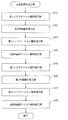
(実施の形態1)
以下、図1~図9を用いて、実施の形態1を説明する。 (Embodiment 1)
The first embodiment will be described below with reference to FIGS.
以下、図1~図9を用いて、実施の形態1を説明する。 (Embodiment 1)
The first embodiment will be described below with reference to FIGS.
[1-1.太陽電池モジュールの構成]
まず、本実施の形態に係る太陽電池モジュールの概略構成について、図1及び図2を用いて説明する。 [1-1. Configuration of solar cell module]
First, a schematic configuration of the solar cell module according to the present embodiment will be described with reference to FIGS. 1 and 2.
まず、本実施の形態に係る太陽電池モジュールの概略構成について、図1及び図2を用いて説明する。 [1-1. Configuration of solar cell module]
First, a schematic configuration of the solar cell module according to the present embodiment will be described with reference to FIGS. 1 and 2.
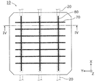
図1は、本実施の形態に係る太陽電池モジュール1の平面図である。図2は、図1のII-II線における太陽電池モジュール1の断面図である。
FIG. 1 is a plan view of a solar cell module 1 according to the present embodiment. FIG. 2 is a cross-sectional view of the solar cell module 1 taken along line II-II in FIG.
図1及び図2に示すように、太陽電池モジュール1は、複数の太陽電池セル10と、配線部材20と、表面保護部材30と、裏面保護部材40と、充填部材50と、フレーム60とを備える。太陽電池モジュール1は、表面保護部材30と裏面保護部材40との間に、複数の太陽電池セル10が充填部材50で封止された構造となっている。
As shown in FIGS. 1 and 2, the solar cell module 1 includes a plurality of solar cells 10, a wiring member 20, a surface protection member 30, a back surface protection member 40, a filling member 50, and a frame 60. Prepare. The solar cell module 1 has a structure in which a plurality of solar cells 10 are sealed with a filling member 50 between a front surface protection member 30 and a back surface protection member 40.
図1に示すように、太陽電池モジュール1の平面視形状は、例えば、略長方形状である。
As shown in FIG. 1, the planar view shape of the solar cell module 1 is, for example, a substantially rectangular shape.
以下、太陽電池モジュール1の各構成部材について、図1及び図2を参照しながら、図3及び図4を用いてさらに詳細に説明する。
Hereinafter, each component of the solar cell module 1 will be described in more detail with reference to FIGS. 3 and 4 with reference to FIGS. 1 and 2.
[1-1-1.太陽電池セル]
太陽電池セル10は、太陽光等の光を電力に変換する光電変換素子(光起電力素子)である。図1に示すように、太陽電池セル10は、同一平面において行列状(マトリクス状)に複数枚配列されている。なお、太陽電池セル10は、同一平面において1行又は1列のみ配列されていてもよい。 [1-1-1. Solar cell]
Thesolar cell 10 is a photoelectric conversion element (photovoltaic element) that converts light such as sunlight into electric power. As shown in FIG. 1, a plurality of solar cells 10 are arranged in a matrix (matrix shape) on the same plane. Note that the solar cells 10 may be arranged in only one row or one column on the same plane.
太陽電池セル10は、太陽光等の光を電力に変換する光電変換素子(光起電力素子)である。図1に示すように、太陽電池セル10は、同一平面において行列状(マトリクス状)に複数枚配列されている。なお、太陽電池セル10は、同一平面において1行又は1列のみ配列されていてもよい。 [1-1-1. Solar cell]
The
直線状に配列された複数の太陽電池セル10は、隣り合う2つの太陽電池セル10同士が配線部材20によって連結されてストリング(セルストリング)を構成している。1つのストリング10S内の複数の太陽電池セル10は、配線部材20によって電気的に接続され、直列接続されている。
The plurality of solar cells 10 arranged in a straight line form a string (cell string) by connecting two adjacent solar cells 10 with a wiring member 20. The plurality of solar cells 10 in one string 10S are electrically connected by the wiring member 20 and are connected in series.
図1に示すように、本実施の形態では、行方向(X軸方向)に沿って等間隔に配列された12枚の太陽電池セル10が配線部材20で接続されることで1つのストリング10Sを構成している。ストリング10Sは、複数形成されている。複数のストリング10S(ストリングス)は、列方向(Y軸方向)に沿って並べられている。本実施の形態では、図1に示すように、6つのストリング10Sが互いに平行となるように列方向に沿って等間隔で並べられている。
As shown in FIG. 1, in the present embodiment, twelve solar cells 10 arranged at equal intervals along the row direction (X-axis direction) are connected by a wiring member 20 to thereby form one string 10S. Is configured. A plurality of strings 10S are formed. The plurality of strings 10S (strings) are arranged along the column direction (Y-axis direction). In the present embodiment, as shown in FIG. 1, the six strings 10S are arranged at equal intervals along the column direction so as to be parallel to each other.
なお、各ストリング10Sは、配線部材20を介して他の配線部材(不図示)に接続されている。これにより、複数のストリング10Sが直列接続又は並列接続されてセルアレイが構成される。本実施の形態では、隣り合う2つのストリング10Sが直列接続されて1つの直列接続体(24枚の太陽電池セル10が直列接続されたもの)が構成されており、この直列接続体が3つ直列接続されて、72枚の太陽電池セルが直列接続されたものが構成されている。
Each string 10S is connected to another wiring member (not shown) via the wiring member 20. Thus, a plurality of strings 10S are connected in series or in parallel to form a cell array. In the present embodiment, two adjacent strings 10S are connected in series to form one series connection body (24 solar cells 10 connected in series), and three series connection bodies are provided. It is connected in series, and 72 solar cells are connected in series.
図1に示すように、複数の太陽電池セル10は、行方向及び列方向に隣り合う太陽電池セル10との間に隙間をあけて配置されている。この隙間には、例えば、光反射部材(不図示)が配置されていてもよい。光反射部材が配置されていると、太陽電池セル10間の隙間領域に入射した光は、光反射部材の表面で反射する。この反射光は、表面保護部材30と太陽電池モジュール1の外部空間との界面で再び反射され、太陽電池セル10上に照射される。よって、太陽電池モジュール1全体の光電変換効率を向上させることが可能となる。
As shown in FIG. 1, the plurality of solar cells 10 are arranged with gaps between the solar cells 10 adjacent in the row direction and the column direction. For example, a light reflecting member (not shown) may be disposed in the gap. When the light reflecting member is disposed, the light incident on the gap region between the solar cells 10 is reflected on the surface of the light reflecting member. The reflected light is reflected again at the interface between the surface protection member 30 and the external space of the solar cell module 1 and irradiated onto the solar cells 10. Therefore, the photoelectric conversion efficiency of the entire solar cell module 1 can be improved.
図3は、本実施の形態に係る太陽電池セル10の一例を示す平面図である。図3に示すように、本実施の形態において、太陽電池セル10の平面視形状は、略矩形状である。例えば、太陽電池セル10は、125mm角の正方形の角が欠けた形状である。つまり、1つのストリング10Sは、隣り合う2つの太陽電池セル10の一辺同士が対向するように構成されている。なお、太陽電池セル10の形状は、略矩形状に限定されない。
FIG. 3 is a plan view showing an example of the solar battery cell 10 according to the present embodiment. As shown in FIG. 3, in this Embodiment, the planar view shape of the photovoltaic cell 10 is substantially rectangular shape. For example, the solar battery cell 10 has a shape in which a 125 mm square square is missing. That is, one string 10 </ b> S is configured such that one side of two adjacent solar battery cells 10 faces each other. In addition, the shape of the photovoltaic cell 10 is not limited to a substantially rectangular shape.
図4は、本実施の形態に係る太陽電池セル10の一例を示す断面図である。具体的には、図4は、図3のIV-IV線における太陽電池セル10の断面図である。図4に示すように、太陽電池セル10は、半導体pn接合を基本構造としており、一例として、n型の半導体基板であるn型単結晶シリコン基板10dと、n型単結晶シリコン基板10dの一方の主面側に順次形成された、n型非晶質シリコン層10b及びn側電極10aと、n型単結晶シリコン基板10dの他方の主面側に順次形成された、p型非晶質シリコン層10f及びp側電極10gとによって構成されている。n側電極10a及びp側電極10gは、例えば、ITO(Indium Tin Oxide)等の透明電極である。また、n型単結晶シリコン基板10dとn型非晶質シリコン層10bとの間にはパッシベーション層であるi型非晶質シリコン層10cが設けられ、n型単結晶シリコン基板10dとp型非晶質シリコン層10fとの間にはパッシベーション層であるi型非晶質シリコン層10eが設けられている。つまり、太陽電池セル10は、例えば、ヘテロ接合型の太陽電池セルである。これにより、n型単結晶シリコン基板10dとn型非晶質シリコン層10bとの界面、及び、n型単結晶シリコン基板10dとp型非晶質シリコン層10fとの界面(ヘテロ接合界面)での欠陥が低減する。よって、太陽電池モジュール1の光電変換効率を向上させることができる。
FIG. 4 is a cross-sectional view showing an example of the solar battery cell 10 according to the present embodiment. Specifically, FIG. 4 is a cross-sectional view of the solar battery cell 10 taken along line IV-IV in FIG. As shown in FIG. 4, the solar cell 10 has a semiconductor pn junction as a basic structure. As an example, one of an n-type single crystal silicon substrate 10d and an n-type single crystal silicon substrate 10d, which is an n-type semiconductor substrate. N-type amorphous silicon layer 10b and n-side electrode 10a sequentially formed on the main surface side of the n-type, and p-type amorphous silicon sequentially formed on the other main surface side of the n-type single crystal silicon substrate 10d. The layer 10f and the p-side electrode 10g are configured. The n-side electrode 10a and the p-side electrode 10g are, for example, transparent electrodes such as ITO (Indium Tin Oxide). Further, an i-type amorphous silicon layer 10c, which is a passivation layer, is provided between the n-type single crystal silicon substrate 10d and the n-type amorphous silicon layer 10b. An i-type amorphous silicon layer 10e, which is a passivation layer, is provided between the crystalline silicon layer 10f. That is, the solar battery cell 10 is, for example, a heterojunction solar battery cell. Thereby, at the interface between the n-type single crystal silicon substrate 10d and the n-type amorphous silicon layer 10b and at the interface (heterojunction interface) between the n-type single crystal silicon substrate 10d and the p-type amorphous silicon layer 10f. Defects are reduced. Therefore, the photoelectric conversion efficiency of the solar cell module 1 can be improved.
なお、パッシベーション層は、i型非晶質シリコン層10c、10eに限定されず、酸化シリコン層又は窒化シリコン層等でもよいし、設けられなくてもよい。また、太陽電池セル10を構成する結晶系シリコン基板は単結晶シリコン基板(n型単結晶シリコン基板、又は、p型単結晶シリコン基板)に限定されず、多結晶シリコン基板等の結晶系シリコン基板(以降、シリコン基板)であればよい。以降の説明において、結晶系シリコン基板が、n型単結晶シリコン基板である場合について説明する。また、結晶系シリコン基板を単にシリコン基板10dと表記する。
Note that the passivation layer is not limited to the i-type amorphous silicon layers 10c and 10e, and may be a silicon oxide layer, a silicon nitride layer, or the like, or may not be provided. The crystalline silicon substrate constituting the solar battery cell 10 is not limited to a single crystal silicon substrate (n-type single crystal silicon substrate or p-type single crystal silicon substrate), but a crystalline silicon substrate such as a polycrystalline silicon substrate. (Hereinafter referred to as a silicon substrate). In the following description, the case where the crystalline silicon substrate is an n-type single crystal silicon substrate will be described. The crystalline silicon substrate is simply referred to as a silicon substrate 10d.
また、本実施の形態において、シリコン基板10dの一方の主面とは、太陽電池モジュール1の主受光面側のシリコン基板10dの面(Z軸プラス側の面)である。シリコン基板10dの他方の主面とは、一方の主面と背向するシリコン基板10dの面(Z軸マイナス側の面)である。
In the present embodiment, the one main surface of the silicon substrate 10d is the surface (the surface on the Z axis plus side) of the silicon substrate 10d on the main light receiving surface side of the solar cell module 1. The other main surface of the silicon substrate 10d is a surface (a surface on the negative side of the Z axis) of the silicon substrate 10d facing away from the one main surface.
図4に示すように、シリコン基板10dの一方の主面(表面)及び他方の主面(裏面)には、テクスチャ構造と呼ばれる凹凸形状が形成されている。テクスチャ構造が形成された一方の主面を第1主面、他方の主面を第2主面とする。そして、シリコン基板10dの第1主面及び第2主面に形成される非晶質シリコン層90、91及び電極10a、10gも、テクスチャ構造を反映した凹凸形状を有している。本実施の形態では、シリコン基板10dの第1主面及び第2主面がテクスチャ構造を有する例について説明するが、これに限定されない。例えば、第1主面のみが上記のテクスチャ構造を有していてもよい。シリコン基板10dと非晶質シリコン層との界面については、後述する。
As shown in FIG. 4, an uneven shape called a texture structure is formed on one main surface (front surface) and the other main surface (back surface) of the silicon substrate 10d. One main surface on which the texture structure is formed is a first main surface, and the other main surface is a second main surface. The amorphous silicon layers 90 and 91 and the electrodes 10a and 10g formed on the first main surface and the second main surface of the silicon substrate 10d also have an uneven shape reflecting the texture structure. In the present embodiment, an example in which the first main surface and the second main surface of the silicon substrate 10d have a texture structure will be described, but the present invention is not limited to this. For example, only the first main surface may have the above texture structure. The interface between the silicon substrate 10d and the amorphous silicon layer will be described later.
なお、上記ではヘテロ接合型の太陽電池セルについて説明したが、太陽電池セル10はヘテロ接合型に限定されない。例えば、太陽電池セル10は単結晶シリコン型又は多結晶シリコン型等の結晶シリコン型の太陽電池セルでもよい。また、例えば、シリコン基板10dの厚みは150μm以下である。
In addition, although the heterojunction type solar cell has been described above, the solar cell 10 is not limited to the heterojunction type. For example, the solar cell 10 may be a crystalline silicon type solar cell such as a single crystal silicon type or a polycrystalline silicon type. For example, the thickness of the silicon substrate 10d is 150 μm or less.
本実施の形態において、太陽電池セル10は、n側電極10aが太陽電池モジュール1の主受光面側(表面保護部材30側)となるように配置されているが、これに限定されない。例えば、p側電極10gが太陽電池モジュール1の主受光面側となるように配置されていてもよい。また、太陽電池モジュール1が片面受光方式である場合には、裏面側に位置する電極(本実施の形態ではp側電極10g)は透明である必要はなく、例えば反射性を有する金属電極であってもよい。
In the present embodiment, the solar cell 10 is arranged so that the n-side electrode 10a is on the main light receiving surface side (surface protection member 30 side) of the solar cell module 1, but the present invention is not limited to this. For example, the p-side electrode 10g may be arranged on the main light receiving surface side of the solar cell module 1. Further, when the solar cell module 1 is of the single-sided light receiving method, the electrode located on the back side (p-side electrode 10g in the present embodiment) does not need to be transparent, for example, a reflective metal electrode. May be.
各太陽電池セル10において、表面は表面保護部材30側の面であり、裏面は裏面保護部材40側の面である。図2に示すように、太陽電池セル10には、表面集電極11と裏面集電極12とが形成されている。表面集電極11は、太陽電池セル10の表面側電極(例えばn側電極10a)に電気的に接続される。裏面集電極12は、太陽電池セル10の裏面側電極(例えばp側電極10g)に電気的に接続される。
In each solar cell 10, the surface is the surface on the surface protection member 30 side, and the back surface is the surface on the back surface protection member 40 side. As shown in FIG. 2, the front surface collecting electrode 11 and the back surface collecting electrode 12 are formed in the solar battery cell 10. The surface collection electrode 11 is electrically connected to the surface side electrode (for example, n side electrode 10a) of the photovoltaic cell 10. The back surface collection electrode 12 is electrically connected to the back surface side electrode (for example, p side electrode 10g) of the photovoltaic cell 10. FIG.
表面集電極11及び裏面集電極12の各々は、例えば、配線部材20の延設方向と直交するように直線状に形成された複数本のフィンガー電極70と、これらのフィンガー電極70に接続されるとともにフィンガー電極70に直交する方向(配線部材20の延設方向)に沿って直線状に形成された複数本のバスバー電極80とによって構成されている。バスバー電極80の本数は、例えば、配線部材20と同数であり、本実施の形態では、3本である。なお、表面集電極11及び裏面集電極12は、互いに同じ形状となっているが、これに限定されない。また、図3に示すように、表面集電極11を構成するとバスバー電極80それぞれの上には、配線部材20が接合される。配線部材20の詳細は、後述する。
Each of the front surface collecting electrode 11 and the back surface collecting electrode 12 is connected to, for example, a plurality of finger electrodes 70 formed linearly so as to be orthogonal to the extending direction of the wiring member 20, and these finger electrodes 70. In addition, a plurality of bus bar electrodes 80 formed linearly along a direction orthogonal to the finger electrodes 70 (extending direction of the wiring member 20). For example, the number of bus bar electrodes 80 is the same as that of the wiring member 20, and is three in the present embodiment. The front collector electrode 11 and the rear collector electrode 12 have the same shape as each other, but are not limited thereto. As shown in FIG. 3, when the surface collector electrode 11 is configured, the wiring member 20 is bonded on each of the bus bar electrodes 80. Details of the wiring member 20 will be described later.
表面集電極11及び裏面集電極12は、銀(Ag)等の低抵抗導電材料からなる。例えば、表面集電極11及び裏面集電極12は、バインダ樹脂中に銀等の導電性フィラーが分散した導電性ペースト(銀ペースト等)を所定のパターンでスクリーン印刷することで形成することができる。
The front collector electrode 11 and the rear collector electrode 12 are made of a low resistance conductive material such as silver (Ag). For example, the front collector electrode 11 and the rear collector electrode 12 can be formed by screen printing a conductive paste (silver paste or the like) in which a conductive filler such as silver is dispersed in a binder resin in a predetermined pattern.
このように構成される太陽電池セル10は、表面及び裏面の両方が受光面となる。太陽電池セル10に光が入射すると太陽電池セル10の光電変換部でキャリアが発生する。発生したキャリアは、表面集電極11及び裏面集電極12で収集されて配線部材20に流れ込む。このように、表面集電極11及び裏面集電極12を設けることで、太陽電池セル10で発生したキャリアを外部回路に効率的に取り出すことができる。
The solar battery cell 10 configured in this way has both the front surface and the back surface as light receiving surfaces. When light enters the solar battery cell 10, carriers are generated in the photoelectric conversion part of the solar battery cell 10. The generated carriers are collected by the front surface collecting electrode 11 and the back surface collecting electrode 12 and flow into the wiring member 20. As described above, by providing the front collector electrode 11 and the rear collector electrode 12, carriers generated in the solar battery cell 10 can be efficiently taken out to an external circuit.
[1-1-2.配線部材(インターコネクタ)]
図1及び図2に示すように、配線部材20(インターコネクタ)は、ストリング10Sにおいて、隣り合う2つの太陽電池セル10同士を電気的に接続するタブ配線である。図1に示すように、本実施の形態では、隣り合う2つの太陽電池セル10は、互いに略平行に配置された3本の配線部材20によって接続されている。各配線部材20は、接続する2つの太陽電池セル10の並び方向に沿って延設されている。図2に示すように、各配線部材20については、配線部材20の一端部が、隣り合う2つの太陽電池セル10のうちの一方の太陽電池セル10の表面に配置され、配線部材20の他端部が、隣り合う2つの太陽電池セル10のうちの他方の太陽電池セル10の裏面に配置されている。各配線部材20は、隣り合う2つの太陽電池セル10において、一方の太陽電池セル10の表面集電極11と、他方の太陽電池セル10の裏面集電極12とを電気的に接続している。例えば、配線部材20と、太陽電池セル10の表面集電極11及び裏面集電極12のバスバー電極80とは、ハンダ材等の導電性を有する接着剤や、樹脂接着材で接合されている。配線部材20と太陽電池セル10の表面集電極11及び裏面集電極12のバスバー電極80とを樹脂接着材で接合する場合、樹脂接着材は導電性粒子を含んでもよい。 [1-1-2. Wiring member (interconnector)]
As shown in FIG.1 and FIG.2, the wiring member 20 (interconnector) is a tab wiring which electrically connects two adjacentphotovoltaic cells 10 in the string 10S. As shown in FIG. 1, in this Embodiment, the two adjacent photovoltaic cells 10 are connected by the three wiring members 20 arrange | positioned mutually substantially parallel. Each wiring member 20 is extended along the alignment direction of the two photovoltaic cells 10 to be connected. As shown in FIG. 2, for each wiring member 20, one end of the wiring member 20 is disposed on the surface of one of the two adjacent solar cells 10, and the other of the wiring members 20. The end portion is disposed on the back surface of the other solar battery cell 10 of the two adjacent solar battery cells 10. Each wiring member 20 electrically connects the front surface collector electrode 11 of one solar cell 10 and the back surface collector electrode 12 of the other solar cell 10 in two adjacent solar cells 10. For example, the wiring member 20 and the front surface collecting electrode 11 of the solar battery cell 10 and the bus bar electrode 80 of the back surface collecting electrode 12 are joined by a conductive adhesive such as a solder material or a resin adhesive. When the wiring member 20 and the front surface collecting electrode 11 of the solar battery cell 10 and the bus bar electrode 80 of the back surface collecting electrode 12 are joined with a resin adhesive, the resin adhesive may include conductive particles.
図1及び図2に示すように、配線部材20(インターコネクタ)は、ストリング10Sにおいて、隣り合う2つの太陽電池セル10同士を電気的に接続するタブ配線である。図1に示すように、本実施の形態では、隣り合う2つの太陽電池セル10は、互いに略平行に配置された3本の配線部材20によって接続されている。各配線部材20は、接続する2つの太陽電池セル10の並び方向に沿って延設されている。図2に示すように、各配線部材20については、配線部材20の一端部が、隣り合う2つの太陽電池セル10のうちの一方の太陽電池セル10の表面に配置され、配線部材20の他端部が、隣り合う2つの太陽電池セル10のうちの他方の太陽電池セル10の裏面に配置されている。各配線部材20は、隣り合う2つの太陽電池セル10において、一方の太陽電池セル10の表面集電極11と、他方の太陽電池セル10の裏面集電極12とを電気的に接続している。例えば、配線部材20と、太陽電池セル10の表面集電極11及び裏面集電極12のバスバー電極80とは、ハンダ材等の導電性を有する接着剤や、樹脂接着材で接合されている。配線部材20と太陽電池セル10の表面集電極11及び裏面集電極12のバスバー電極80とを樹脂接着材で接合する場合、樹脂接着材は導電性粒子を含んでもよい。 [1-1-2. Wiring member (interconnector)]
As shown in FIG.1 and FIG.2, the wiring member 20 (interconnector) is a tab wiring which electrically connects two adjacent
配線部材20は、長尺状の導電性配線であって、例えば、リボン状の金属箔である。配線部材20は、例えば、銅箔や銀箔等の金属箔の表面全体を半田や銀等で被覆したものを所定の長さに短冊状に切断することによって作製することができる。
The wiring member 20 is a long conductive wiring, for example, a ribbon-shaped metal foil. The wiring member 20 can be produced by, for example, cutting a metal foil such as a copper foil or a silver foil, which is entirely covered with solder, silver, or the like into a strip shape having a predetermined length.
[1-1-3.表面保護部材、裏面保護部材]
表面保護部材30は、太陽電池モジュール1の表側の面を保護する部材であり、太陽電池モジュール1の内部(太陽電池セル10等)を、風雨や外部衝撃等の外部環境から保護する。図2に示すように、表面保護部材30は、太陽電池セル10の表面側に配設されており、太陽電池セル10の表面側の受光面を保護している。 [1-1-3. Surface protection member, back surface protection member]
Thesurface protection member 30 is a member that protects the front side surface of the solar cell module 1 and protects the inside of the solar cell module 1 (solar cell 10 or the like) from an external environment such as wind and rain or external impact. As shown in FIG. 2, the surface protection member 30 is disposed on the surface side of the solar cell 10 and protects the light receiving surface on the surface side of the solar cell 10.
表面保護部材30は、太陽電池モジュール1の表側の面を保護する部材であり、太陽電池モジュール1の内部(太陽電池セル10等)を、風雨や外部衝撃等の外部環境から保護する。図2に示すように、表面保護部材30は、太陽電池セル10の表面側に配設されており、太陽電池セル10の表面側の受光面を保護している。 [1-1-3. Surface protection member, back surface protection member]
The
表面保護部材30は、太陽電池セル10において光電変換に利用される波長帯域の光を透過する透光性部材によって構成されている。表面保護部材30は、例えば、透明ガラス材料からなるガラス基板(透明ガラス基板)、又は、フィルム状や板状の透光性及び遮水性を有する硬質の樹脂材料からなる樹脂基板である。
The surface protection member 30 is configured by a translucent member that transmits light in a wavelength band used for photoelectric conversion in the solar battery cell 10. The surface protection member 30 is, for example, a glass substrate (transparent glass substrate) made of a transparent glass material, or a resin substrate made of a hard resin material having a film-like or plate-like translucency and water shielding property.
一方、裏面保護部材40は、太陽電池モジュール1の裏側の面を保護する部材であり、太陽電池モジュール1の内部を外部環境から保護する。図2に示すように、裏面保護部材40は、太陽電池セル10の裏面側に配設されており、太陽電池セル10の裏面側の受光面を保護している。
On the other hand, the back surface protection member 40 is a member that protects the back surface of the solar cell module 1 and protects the inside of the solar cell module 1 from the external environment. As shown in FIG. 2, the back surface protection member 40 is disposed on the back surface side of the solar battery cell 10 and protects the light receiving surface on the back surface side of the solar battery cell 10.
裏面保護部材40は、例えば、ポリエチレンテレフタレート(PET)又はポリエチレンナフタレート(PEN)等の樹脂材料からなるフィルム状や板状の樹脂シートである。
The back surface protection member 40 is a film-like or plate-like resin sheet made of a resin material such as polyethylene terephthalate (PET) or polyethylene naphthalate (PEN).
太陽電池モジュール1が片面受光方式である場合には、裏面保護部材40は、不透光の板体又はフィルムとしてもよい。なお、裏面保護部材40は、不透光部材に限るものではなく、ガラス材料からなるガラスシート又はガラス基板等の透光性部材であってもよい。
When the solar cell module 1 is a single-sided light receiving method, the back surface protection member 40 may be an opaque plate or film. In addition, the back surface protection member 40 is not restricted to an opaque member, and may be a transparent member such as a glass sheet or a glass substrate made of a glass material.
[1-1-4.充填部材]
表面保護部材30及び裏面保護部材40の間には充填部材50が充填されている。表面保護部材30及び裏面保護部材40と太陽電池セル10とは、この充填部材50によって接着されて固定されている。本実施の形態において、充填部材50は、表面保護部材30と裏面保護部材40との間を埋めるように充填されている。 [1-1-4. Filling member]
A fillingmember 50 is filled between the front surface protection member 30 and the back surface protection member 40. The front surface protection member 30, the back surface protection member 40, and the solar battery cell 10 are bonded and fixed by the filling member 50. In the present embodiment, the filling member 50 is filled so as to fill a space between the front surface protection member 30 and the back surface protection member 40.
表面保護部材30及び裏面保護部材40の間には充填部材50が充填されている。表面保護部材30及び裏面保護部材40と太陽電池セル10とは、この充填部材50によって接着されて固定されている。本実施の形態において、充填部材50は、表面保護部材30と裏面保護部材40との間を埋めるように充填されている。 [1-1-4. Filling member]
A filling
図2に示すように、充填部材50は、表面充填部材51と裏面充填部材52とによって構成されている。表面充填部材51及び裏面充填部材52の各々は、マトリクス状に配置された複数の太陽電池セル10を覆っている。
As shown in FIG. 2, the filling member 50 includes a front surface filling member 51 and a back surface filling member 52. Each of the surface filling member 51 and the back surface filling member 52 covers the plurality of solar cells 10 arranged in a matrix.
複数の太陽電池セル10は、例えばシート状の表面充填部材51と裏面充填部材52とで挟み込まれた状態でラミネート処理(ラミネート加工)を行うことで充填部材50によって全体が覆われる。
The plurality of solar cells 10 are entirely covered with the filling member 50 by performing a laminating process (lamination process) while being sandwiched between, for example, a sheet-like surface filling member 51 and a back surface filling member 52.
具体的には、複数の太陽電池セル10を配線部材20で連結してストリング10Sを形成した後、複数本のストリング10Sを表面充填部材51と裏面充填部材52とで挟み込み、さらに、その上下に表面保護部材30と裏面保護部材40とを配置して、例えば100℃以上の温度で真空中で熱圧着を行う。この熱圧着によって、表面充填部材51及び裏面充填部材52が加熱されて溶融し、太陽電池セル10を封止する充填部材50となる。
Specifically, after a plurality of solar cells 10 are connected by the wiring member 20 to form the string 10S, the plurality of strings 10S are sandwiched between the surface filling member 51 and the back surface filling member 52, and further above and below the string 10S. The surface protection member 30 and the back surface protection member 40 are arranged, and thermocompression bonding is performed in a vacuum at a temperature of 100 ° C. or higher, for example. By this thermocompression bonding, the front surface filling member 51 and the back surface filling member 52 are heated and melted to form the filling member 50 that seals the solar battery cell 10.
ラミネート処理前の表面充填部材51は、例えば、エチレンビニールアセテート(EVA)又はポリオレフィン等の樹脂材料によって構成された樹脂シートであり、複数の太陽電池セル10と表面保護部材30との間に配置される。表面充填部材51は、ラミネート処理によって主に太陽電池セル10と表面保護部材30との間の隙間を埋めるように充填される。
The surface filling member 51 before laminating is, for example, a resin sheet made of a resin material such as ethylene vinyl acetate (EVA) or polyolefin, and is disposed between the plurality of solar cells 10 and the surface protection member 30. The The surface filling member 51 is mainly filled by laminating so as to fill a gap between the solar battery cell 10 and the surface protection member 30.
表面充填部材51は、透光性材料によって構成されている。本実施の形態では、ラミネート処理前の表面充填部材51として、EVAからなる透明樹脂シートを用いている。
The surface filling member 51 is made of a translucent material. In the present embodiment, a transparent resin sheet made of EVA is used as the surface filling member 51 before the lamination process.
ラミネート処理前の裏面充填部材52は、例えばEVA又はポリオレフィン等の樹脂材料によって構成された樹脂シートであり、複数の太陽電池セル10と裏面保護部材40との間に配置される。裏面充填部材52は、ラミネート処理によって主に太陽電池セル10と裏面保護部材40との間の隙間を埋めるように充填される。
The back surface filling member 52 before the lamination process is a resin sheet made of a resin material such as EVA or polyolefin, and is disposed between the plurality of solar cells 10 and the back surface protection member 40. The back surface filling member 52 is mainly filled by laminating so as to fill a gap between the solar battery cell 10 and the back surface protection member 40.
なお、本実施の形態における太陽電池モジュール1は片面受光方式であってもよく、片面受光方式である場合には、裏面充填部材52は、透光性材料に限るものではなく、黒色材料又は白色材料等の着色材料によって構成されていてもよい。
Note that the solar cell module 1 in the present embodiment may be of a single-sided light receiving method, and in the case of the single-sided light receiving method, the back surface filling member 52 is not limited to a light-transmitting material, but a black material or white You may be comprised with coloring materials, such as material.
[1-1-5.フレーム]
フレーム60は、太陽電池モジュール1の周縁端部を覆う外枠である。フレーム60は、例えば、アルミ製のアルミフレーム(アルミ枠)である。図1に示すように、フレーム60は、4本用いられており、それぞれ太陽電池モジュール1の4辺の各々に装着されている。フレーム60は、例えば、接着剤によって太陽電池モジュール1の各辺に固着されている。 [1-1-5. flame]
Theframe 60 is an outer frame that covers the peripheral edge of the solar cell module 1. The frame 60 is, for example, an aluminum frame (aluminum frame) made of aluminum. As shown in FIG. 1, four frames 60 are used, and are attached to each of the four sides of the solar cell module 1. The frame 60 is fixed to each side of the solar cell module 1 with an adhesive, for example.
フレーム60は、太陽電池モジュール1の周縁端部を覆う外枠である。フレーム60は、例えば、アルミ製のアルミフレーム(アルミ枠)である。図1に示すように、フレーム60は、4本用いられており、それぞれ太陽電池モジュール1の4辺の各々に装着されている。フレーム60は、例えば、接着剤によって太陽電池モジュール1の各辺に固着されている。 [1-1-5. flame]
The
[1-2.太陽電池セルの詳細]
続いて、本実施の形態に係る太陽電池セル10の詳細構成について、図5A~図6Bを用いて説明する。 [1-2. Details of solar cells]
Next, the detailed configuration of thesolar battery cell 10 according to the present embodiment will be described with reference to FIGS. 5A to 6B.
続いて、本実施の形態に係る太陽電池セル10の詳細構成について、図5A~図6Bを用いて説明する。 [1-2. Details of solar cells]
Next, the detailed configuration of the
[1-2-1.シリコン基板の表面構造]
まずは、図5A及び図5Bを用いて、本実施の形態に係るシリコン基板10dの表面構造について説明する。 [1-2-1. Surface structure of silicon substrate]
First, the surface structure of thesilicon substrate 10d according to the present embodiment will be described with reference to FIGS. 5A and 5B.
まずは、図5A及び図5Bを用いて、本実施の形態に係るシリコン基板10dの表面構造について説明する。 [1-2-1. Surface structure of silicon substrate]
First, the surface structure of the
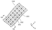
図5Aは、本実施の形態に係るシリコン基板10dに形成されるテクスチャ構造の拡大平面を示す模式図である。図5Bは、図5AのVb-Vb線におけるシリコン基板10dの断面図である。なお、図5Aは、第1主面におけるテクスチャ構造の模式図である。
FIG. 5A is a schematic diagram showing an enlarged plane of the texture structure formed on the silicon substrate 10d according to the present embodiment. FIG. 5B is a cross-sectional view of the silicon substrate 10d taken along the line Vb-Vb in FIG. 5A. FIG. 5A is a schematic diagram of the texture structure on the first main surface.
図5Aに示すように、シリコン基板10dの第1主面は、複数の角錐が2次元状に配置されたテクスチャ構造(凹凸)を有している。図5Bに示すように、テクスチャ構造は、四角錐の基板頂部101及び隣接する基板頂部101で挟まれた基板谷部102を有している。本実施の形態では、基板頂部101と基板谷部102との間の角錐面はシリコン結晶の(111)面となっている。なお、第2主面も、第1主面と同様、テクスチャ構造を有していてもよい。
As shown in FIG. 5A, the first main surface of the silicon substrate 10d has a texture structure (unevenness) in which a plurality of pyramids are two-dimensionally arranged. As shown in FIG. 5B, the texture structure has a substrate pyramid 102 sandwiched between a quadrangular pyramid substrate top 101 and an adjacent substrate top 101. In the present embodiment, the pyramid surface between the substrate top portion 101 and the substrate valley portion 102 is a (111) plane of silicon crystal. In addition, the 2nd main surface may also have a texture structure similarly to the 1st main surface.
また、基板谷部102から基板頂部101までの高さは、例えば、1μm以上10μm以下であり、隣接する基板頂部101の間隔は、例えば、1μm以上10μm以下である。なお、本実施の形態に係るシリコン基板10dのテクスチャ構造では、基板頂部101及び基板谷部102の高さ及びピッチはランダムであってもよいし、規則的であってもよい。
Further, the height from the substrate valley 102 to the substrate top 101 is, for example, 1 μm or more and 10 μm or less, and the interval between adjacent substrate tops 101 is, for example, 1 μm or more and 10 μm or less. In the texture structure of the silicon substrate 10d according to the present embodiment, the height and pitch of the substrate top portion 101 and the substrate valley portion 102 may be random or regular.
また、シリコン基板10dの第1主面及び第2主面が有するテクスチャ構造の例について説明したが、第1主面及び第2主面が有するテクスチャ構造の形状は同じでもよいし、異なっていてもよい。例えば、第1主面及び第2主面に入射する光の角度は異なるので、それぞれの主面に入射する光の角度に合わせてテクスチャ構造の形状が決定されてもよい。
Moreover, although the example of the texture structure which the 1st main surface and the 2nd main surface of the silicon substrate 10d have was demonstrated, the shape of the texture structure which the 1st main surface and the 2nd main surface have may be the same, and are different. Also good. For example, since the angles of light incident on the first main surface and the second main surface are different, the shape of the texture structure may be determined according to the angle of light incident on each main surface.
[1-2-2.非晶質シリコン層の構造]
次に、図6A及び図6Bを用いて、シリコン基板10dの主面上に形成される非晶質シリコン層について説明する。なお、第1主面及び第2主面における非晶質シリコン層の構造は実質的には同じであり、第1主面についてのみ説明する。 [1-2-2. Structure of amorphous silicon layer]
Next, an amorphous silicon layer formed on the main surface of thesilicon substrate 10d will be described with reference to FIGS. 6A and 6B. The structure of the amorphous silicon layer on the first main surface and the second main surface is substantially the same, and only the first main surface will be described.
次に、図6A及び図6Bを用いて、シリコン基板10dの主面上に形成される非晶質シリコン層について説明する。なお、第1主面及び第2主面における非晶質シリコン層の構造は実質的には同じであり、第1主面についてのみ説明する。 [1-2-2. Structure of amorphous silicon layer]
Next, an amorphous silicon layer formed on the main surface of the
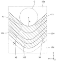
図6Aは、図4の破線領域VIaにおける拡大断面図である。具体的には、図6Aは、シリコン基板10d、第1非晶質シリコン層90及びn側電極10aの谷部付近の積層構造を拡大した断面図である。図6Aの断面図は、第1非晶質シリコン層90の頂部(図示しない)及び谷部103(図7参照)を結ぶ傾斜部104(図7参照)と、隣接する2つの傾斜部104に挟まれた谷部103とを示している。図6Bは、図6Aの破線領域VIbにおける拡大断面図である。
FIG. 6A is an enlarged cross-sectional view taken along a broken line area VIa in FIG. Specifically, FIG. 6A is an enlarged cross-sectional view of the laminated structure in the vicinity of the valleys of the silicon substrate 10d, the first amorphous silicon layer 90, and the n-side electrode 10a. 6A shows a slope 104 (see FIG. 7) connecting the top (not shown) and the valley 103 (see FIG. 7) of the first amorphous silicon layer 90 and two slopes 104 adjacent to each other. A valley portion 103 sandwiched therebetween is shown. FIG. 6B is an enlarged cross-sectional view taken along broken line area VIb in FIG. 6A.
図6Aに示すように、第1非晶質シリコン層90は、i型非晶質シリコン層10c及びn型非晶質シリコン層10bにより構成される。本実施の形態では、i型非晶質シリコン層10cは3層構造を有している。本実施の形態では、i型非晶質シリコン層10cにおいて、第1エピタキシャル層120、第1中間層121及び第1パッシベーション層122が形成される。図6Bに示すように、第1エピタキシャル層120は、エピタキシャル成長した結晶領域120aと非晶質領域120bとを有する。また、第1中間層121及び第1パッシベーション層122は、非晶質(アモルファス)領域のみで構成されており、密度(膜密度)などが異なる。より詳しくは、第1中間層121の密度は、第1パッシベーション層122の密度より低い。なお、密度(膜密度)とは、各層の単位体積(例えば、1立方センチメートル)あたりの質量を意味する。また、n型非晶質シリコン層10bは、本実施の形態では、非晶質領域のみで構成されているパッシベーション層である。第1中間層121及びn型非晶質シリコン層10bは、密度(膜密度)などが異なる。より詳しくは、第1中間層121の密度は、n型非晶質シリコン層10bの密度より低い。
As shown in FIG. 6A, the first amorphous silicon layer 90 includes an i-type amorphous silicon layer 10c and an n-type amorphous silicon layer 10b. In the present embodiment, i-type amorphous silicon layer 10c has a three-layer structure. In the present embodiment, the first epitaxial layer 120, the first intermediate layer 121, and the first passivation layer 122 are formed in the i-type amorphous silicon layer 10c. As shown in FIG. 6B, the first epitaxial layer 120 has an epitaxially grown crystal region 120a and an amorphous region 120b. Further, the first intermediate layer 121 and the first passivation layer 122 are configured only by an amorphous region, and have different densities (film densities). More specifically, the density of the first intermediate layer 121 is lower than the density of the first passivation layer 122. The density (film density) means the mass per unit volume (for example, 1 cubic centimeter) of each layer. In the present embodiment, the n-type amorphous silicon layer 10b is a passivation layer composed of only an amorphous region. The first intermediate layer 121 and the n-type amorphous silicon layer 10b have different densities (film density). More specifically, the density of the first intermediate layer 121 is lower than the density of the n-type amorphous silicon layer 10b.
第1非晶質シリコン層90は、谷部103において、シリコン基板10d上にエピタキシャル成長した結晶領域120aを含む第1エピタキシャル層120と、第1エピタキシャル層120上に形成された非晶質シリコン層である第1中間層121と、第1中間層121上に形成された非晶質シリコン層である第1パッシベーション層122と、第1パッシベーション層122上に形成された非晶質シリコン層であるn型非晶質シリコン層10bとが、シリコン基板10dの第1主面から略垂直方向(Z軸プラス側方向)に向けて積層されている。
The first amorphous silicon layer 90 includes a first epitaxial layer 120 including a crystal region 120a epitaxially grown on the silicon substrate 10d in the valley portion 103, and an amorphous silicon layer formed on the first epitaxial layer 120. A first intermediate layer 121, a first passivation layer 122 that is an amorphous silicon layer formed on the first intermediate layer 121, and an n that is an amorphous silicon layer formed on the first passivation layer 122. A type amorphous silicon layer 10b is laminated in a substantially vertical direction (Z-axis plus side direction) from the first main surface of the silicon substrate 10d.
また、図6Aに示すように、第1非晶質シリコン層90は、シリコン基板10dの第1主面のテクスチャ構造を反映した凹凸形状を有している。また、n側電極10aも当該テクスチャ構造を反映した凹凸形状を有している。
Further, as shown in FIG. 6A, the first amorphous silicon layer 90 has a concavo-convex shape reflecting the texture structure of the first main surface of the silicon substrate 10d. Further, the n-side electrode 10a also has an uneven shape reflecting the texture structure.
図6Bに示すように、本実施の形態では、i型非晶質シリコン層10cの第1エピタキシャル層120は、谷部103において結晶領域120aと非晶質(アモルファス)領域120bとを含んでいる。結晶領域120aは、シリコン基板10dの結晶方位を反映したエピタキシャル成長領域や微細な結晶領域を含んでいてもよい。また、非晶質領域120bは、シリコン基板10dの結晶方位を反映しない、非晶質(アモルファス)で占有された領域である。なお、例えば、第1エピタキシャル層120の導電率は、暗導電率が1.0×10⁻⁷S/cm以上1.0×10-5S/cm以下であり、光導電率が1.0×10-4S/cm以上1.0×10-3S/cm以下である。
As shown in FIG. 6B, in the present embodiment, the first epitaxial layer 120 of the i-type amorphous silicon layer 10c includes a crystalline region 120a and an amorphous (amorphous) region 120b in the valley portion 103. . The crystal region 120a may include an epitaxial growth region or a fine crystal region reflecting the crystal orientation of the silicon substrate 10d. Further, the amorphous region 120b is a region occupied by amorphous material that does not reflect the crystal orientation of the silicon substrate 10d. For example, the conductivity of the first epitaxial layer 120 has a dark conductivity of 1.0 × 10 −7 S / cm or more and 1.0 × 10 −5 S / cm or less, and a photoconductivity of 1.0 × 10 −5 S / cm. × 10 −4 S / cm or more and 1.0 × 10 −3 S / cm or less.
第1エピタキシャル層120が結晶領域120aを含むことで、曲線因子の低下を抑制することができる。また、曲線因子の調整は、第1エピタキシャル層120の厚みを調整することで実現できる。第1エピタキシャル層120の厚みは、成膜する時間により調整することができる。よって、テクスチャ構造が微細化した場合でも、第1エピタキシャル層120の成膜時間を調整するといった簡単な制御で、曲線因子の低下を抑制することができる。つまり、テクスチャ構造が微細化した場合でも、曲線因子を高い状態に維持することができる。
The fall of a fill factor can be suppressed because the 1st epitaxial layer 120 contains the crystal region 120a. Further, the adjustment of the fill factor can be realized by adjusting the thickness of the first epitaxial layer 120. The thickness of the first epitaxial layer 120 can be adjusted by the film formation time. Therefore, even when the texture structure is miniaturized, a decrease in the fill factor can be suppressed by simple control such as adjusting the film formation time of the first epitaxial layer 120. That is, even when the texture structure is refined, the fill factor can be maintained in a high state.
なお、第1エピタキシャル層120における結晶領域120a及び非晶質領域120bの占有率は、特に限定されない。例えば、第1エピタキシャル層120は、結晶領域120aのみから構成されてもよい。例えば、少なくとも谷部103において、第1エピタキシャル層120は結晶領域120aのみから構成されてもよい。結晶領域120aは、第1エピタキシャル層120の主たる構成要素である非晶質領域120bに比べて導電性に優れている。従って、第1エピタキシャル層120において、結晶領域120aの占有率が高いほど、抵抗損失が低減され、曲線因子を向上させることができる。また、占有率とは、太陽電池セル10を断面視した(Y軸方向から見た)場合の第1エピタキシャル層120の谷部103の面積に対する結晶領域120a又は非晶質領域120bの面積の割合である。
Note that the occupation ratio of the crystal region 120a and the amorphous region 120b in the first epitaxial layer 120 is not particularly limited. For example, the first epitaxial layer 120 may be composed only of the crystal region 120a. For example, at least in the valley portion 103, the first epitaxial layer 120 may be composed of only the crystal region 120a. The crystal region 120 a is superior in conductivity to the amorphous region 120 b that is a main component of the first epitaxial layer 120. Therefore, in the first epitaxial layer 120, the higher the occupation ratio of the crystal region 120a, the lower the resistance loss, and the curve factor can be improved. The occupation ratio is the ratio of the area of the crystalline region 120a or the amorphous region 120b to the area of the valley 103 of the first epitaxial layer 120 when the solar battery cell 10 is viewed in cross section (viewed from the Y-axis direction). It is.
また、図6Bでは、第1エピタキシャル層120上に形成される第1中間層121にわたって結晶領域120aが貫通している例を示しているが、これに限定されない。結晶領域120aは、第1中間層121にわたって貫通していなくてもよい。
6B shows an example in which the crystal region 120a passes through the first intermediate layer 121 formed on the first epitaxial layer 120, but the present invention is not limited to this. The crystal region 120 a may not penetrate through the first intermediate layer 121.
続いて、第1エピタキシャル層120の上に積層される第1中間層121について説明する。第1エピタキシャル層120は結晶領域120aを含んでいる。第1中間層121は、成膜される際、第1エピタキシャル層120の結晶領域120aの影響を受けないように形成される。具体的には、第1中間層121を成膜する成膜速度(成膜レート)を、第1エピタキシャル層120を成膜する成膜速度より大きくする。例えば、第1中間層121を成膜する成膜速度は、第1エピタキシャル層120を成膜する成膜速度の3倍などである。これにより、形成される第1中間層121は、第1エピタキシャル層120の結晶領域120aの影響を受けずに成膜される。つまり、第1中間層121は、エピタキシャル成長領域を含まない非晶質領域のみで形成される。また、第1中間層121の成膜速度が大きいので、第1中間層121の密度は、第1エピタキシャル層120の密度より低くなる。なお、第1中間層121は、第1アモルファス層の一例である。
Subsequently, the first intermediate layer 121 stacked on the first epitaxial layer 120 will be described. The first epitaxial layer 120 includes a crystal region 120a. The first intermediate layer 121 is formed so as not to be affected by the crystal region 120a of the first epitaxial layer 120 when it is formed. Specifically, the film formation rate (film formation rate) for forming the first intermediate layer 121 is set higher than the film formation rate for forming the first epitaxial layer 120. For example, the film formation speed for forming the first intermediate layer 121 is three times the film formation speed for forming the first epitaxial layer 120. Thereby, the formed first intermediate layer 121 is formed without being affected by the crystal region 120 a of the first epitaxial layer 120. That is, the first intermediate layer 121 is formed only of an amorphous region that does not include an epitaxial growth region. Further, since the deposition rate of the first intermediate layer 121 is high, the density of the first intermediate layer 121 is lower than the density of the first epitaxial layer 120. The first intermediate layer 121 is an example of a first amorphous layer.
続いて、第1中間層121の上に形成される第1パッシベーション層122について説明する。第1中間層121は非晶質領域のみで形成されている。そのため、第1パッシベーション層122を成膜する際、第1エピタキシャル層120の結晶領域120aの影響を受けずに第1パッシベーション層122が形成される。これにより、第1パッシベーション層122は、非晶質領域のみで形成される。
Subsequently, the first passivation layer 122 formed on the first intermediate layer 121 will be described. The first intermediate layer 121 is formed only of an amorphous region. Therefore, when forming the first passivation layer 122, the first passivation layer 122 is formed without being affected by the crystal region 120a of the first epitaxial layer 120. As a result, the first passivation layer 122 is formed only of the amorphous region.
一般的に、成膜速度を低くすると膜質の良い膜が形成される。つまり、成膜速度を低くすると、高いパッシベーション性を有する膜が形成される。そのため、第1パッシベーション層122は、成膜速度を低くして形成されることが好ましい。例えば、第1パッシベーション層122を成膜する成膜速度は、第1エピタキシャル層120を成膜する成膜速度より低い。これにより、第1パッシベーション層122の密度は、第1エピタキシャル層120の密度より高くなる。
Generally, when the film formation rate is lowered, a film with good film quality is formed. That is, when the deposition rate is lowered, a film having high passivation properties is formed. Therefore, the first passivation layer 122 is preferably formed at a low film formation rate. For example, the deposition rate for forming the first passivation layer 122 is lower than the deposition rate for forming the first epitaxial layer 120. As a result, the density of the first passivation layer 122 is higher than the density of the first epitaxial layer 120.
また、第1パッシベーション層122を成膜する成膜速度を低くすることで、第1パッシベーション層122の導電率は高くなる。例えば、第1パッシベーション層122を成膜する成膜速度を、第1中間層121を成膜する成膜速度より低くすることで、第1パッシベーション層122の導電率は、第1中間層121の導電率より高くなる。例えば、第1中間層121の導電率は、暗導電率が1.0×10⁻¹⁴S/cm以上1.0×10-10S/cm以下であり、光導電率が1.0×10-7S/cm以上1.0×10-4S/cm以下である。また、例えば、第1パッシベーション層122の導電率は、暗導電率が1.0×10-9S/cm以上1.0×10-7S/cm以下であり、光導電率が1.0×10-7S/cm以上1.0×10-4S/cm以下である。つまり、第1パッシベーション層122を形成することで、高いパッシベーション性を維持でき、かつ曲線因子が低下することを抑制することができる。よって、テクスチャ構造が微細化した場合でも、曲線因子の低下を抑制し、かつ、開放電圧を高い状態に維持することができる。
Moreover, the electrical conductivity of the 1st passivation layer 122 becomes high by making the film-forming speed | rate which forms the 1st passivation layer 122 low. For example, by setting the deposition rate for forming the first passivation layer 122 to be lower than the deposition rate for forming the first intermediate layer 121, the conductivity of the first passivation layer 122 can be increased to that of the first intermediate layer 121. It becomes higher than the conductivity. For example, the first intermediate layer 121 has a dark conductivity of 1.0 × 10 −14 S / cm or more and 1.0 × 10 −10 S / cm or less, and a photoconductivity of 1.0 × 10 6. -7 S / cm or more and 1.0 × 10 -4 S / cm or less. Further, for example, the conductivity of the first passivation layer 122 is such that the dark conductivity is 1.0 × 10 −9 S / cm or more and 1.0 × 10 −7 S / cm or less, and the photoconductivity is 1.0. × 10 −7 S / cm or more and 1.0 × 10 −4 S / cm or less. That is, by forming the first passivation layer 122, it is possible to maintain high passivation properties and to suppress a reduction in the fill factor. Therefore, even when the texture structure is miniaturized, it is possible to suppress the decrease of the fill factor and maintain the open circuit voltage at a high level.
なお、第1中間層121は、例えば、第1エピタキシャル層120及び第1パッシベーション層122より導電率が低い。つまり、第1中間層121による抵抗損失が大きい。そのため、第1中間層121が厚いと太陽電池セル10の曲線因子が低下するので、第1中間層121は薄く成膜される方が好ましい。第1中間層121は、第1パッシベーション層122が第1エピタキシャル層120の影響を受けずに成膜できる厚みの中で、極力薄く成膜される方が好ましい。例えば、第1中間層121の厚みは、第1パッシベーション層122の厚みより薄い。例えば、第1中間層121の厚みは、1nm以上3nm以下である。なお、厚みの調整は、第1エピタキシャル層120と同様、成膜する時間で調整できる。
The first intermediate layer 121 has a lower conductivity than the first epitaxial layer 120 and the first passivation layer 122, for example. That is, the resistance loss due to the first intermediate layer 121 is large. For this reason, if the first intermediate layer 121 is thick, the fill factor of the solar battery cell 10 is reduced. Therefore, it is preferable that the first intermediate layer 121 be formed thin. The first intermediate layer 121 is preferably formed as thin as possible within the thickness that allows the first passivation layer 122 to be formed without being affected by the first epitaxial layer 120. For example, the thickness of the first intermediate layer 121 is smaller than the thickness of the first passivation layer 122. For example, the thickness of the first intermediate layer 121 is 1 nm or more and 3 nm or less. Note that the thickness can be adjusted by the time of film formation as in the case of the first epitaxial layer 120.
続いて、第1パッシベーション層122の上に形成されるn型非晶質シリコン層10bについて説明する。第1パッシベーション層122は非晶質領域のみで形成されている。そのため、n型非晶質シリコン層10bを成膜する際、第1エピタキシャル層120の結晶領域120aの影響を受けずにn型非晶質シリコン層10bが形成される。これにより、n型非晶質シリコン層10bは、非晶質領域のみで形成される。また、n型非晶質シリコン層10bは、第1パッシベーション層122と同様、成膜速度を低くして形成されることが好ましい。
Subsequently, the n-type amorphous silicon layer 10b formed on the first passivation layer 122 will be described. The first passivation layer 122 is formed of only an amorphous region. Therefore, when the n-type amorphous silicon layer 10b is formed, the n-type amorphous silicon layer 10b is formed without being affected by the crystal region 120a of the first epitaxial layer 120. Thereby, the n-type amorphous silicon layer 10b is formed only by the amorphous region. In addition, the n-type amorphous silicon layer 10b is preferably formed at a low film formation rate, like the first passivation layer 122.
なお、第1パッシベーション層122及びn型非晶質シリコン層10bは、第2アモルファス層の一例である。第2アモルファス層とは、第1中間層の上に形成される非晶質シリコン層である。なお、n型非晶質シリコン層10bは、第2アモルファス層に含まれなくてもよい。
The first passivation layer 122 and the n-type amorphous silicon layer 10b are examples of the second amorphous layer. The second amorphous layer is an amorphous silicon layer formed on the first intermediate layer. Note that the n-type amorphous silicon layer 10b may not be included in the second amorphous layer.
また、第1非晶質シリコン層90は、谷部103を除く部分において実質的にアモルファス状態である。つまり、n型非晶質シリコン層10b及びi型非晶質シリコン層10c(第1エピタキシャル層120、第1中間層121及び第1パッシベーション層122)は、谷部103以外では、実質的にアモルファス状態である。
Further, the first amorphous silicon layer 90 is substantially in an amorphous state in a portion excluding the valley portion 103. That is, the n-type amorphous silicon layer 10b and the i-type amorphous silicon layer 10c (the first epitaxial layer 120, the first intermediate layer 121, and the first passivation layer 122) are substantially amorphous except for the valley portion 103. State.
次に、第1非晶質シリコン層90における谷部103の範囲について説明する。
Next, the range of the valley 103 in the first amorphous silicon layer 90 will be described.
図7は、本実施の形態に係る第1非晶質シリコン層90の谷部103のアール形状を表す曲率半径を説明する図である。谷部103は、太陽電池セル10を断面視した場合、シリコン基板10dの基板谷部102の形状を反映したアール形状を有している。谷部103は、略直線状の傾斜部104に挟まれた領域である。ここで、谷部103の範囲は、図7に示すように、傾斜部104の傾面の傾きが変化する点X1~X4で挟まれた領域と定義される。例えば、谷部103の曲率半径Rは、1nm以上300nm以下である。なお、谷部103の曲率半径Rとは、2つの点X1及びX2で挟まれた谷部103の曲面とを含む円Cの半径と定義される。
FIG. 7 is a diagram for explaining the radius of curvature representing the round shape of the valley 103 of the first amorphous silicon layer 90 according to the present embodiment. The valley portion 103 has a round shape reflecting the shape of the substrate valley portion 102 of the silicon substrate 10 d when the solar battery cell 10 is viewed in cross section. The valley portion 103 is a region sandwiched between substantially linear inclined portions 104. Here, the range of the valley portion 103 is defined as a region sandwiched between points X1 to X4 where the inclination of the inclined surface of the inclined portion 104 changes, as shown in FIG. For example, the curvature radius R of the valley 103 is 1 nm or more and 300 nm or less. The radius of curvature R of the valley 103 is defined as the radius of a circle C including the curved surface of the valley 103 sandwiched between two points X1 and X2.
[1-3.製造方法]
続いて、本実施の形態に係る太陽電池セル10の製造方法について、図8A~図9を用いて説明する。なお、製造方法では、第1主面及び第2主面の両面に非晶質シリコン層90、91を成膜する場合について説明する。 [1-3. Production method]
Next, a method for manufacturingsolar battery cell 10 according to the present embodiment will be described with reference to FIGS. 8A to 9. In the manufacturing method, a case where amorphous silicon layers 90 and 91 are formed on both the first main surface and the second main surface will be described.
続いて、本実施の形態に係る太陽電池セル10の製造方法について、図8A~図9を用いて説明する。なお、製造方法では、第1主面及び第2主面の両面に非晶質シリコン層90、91を成膜する場合について説明する。 [1-3. Production method]
Next, a method for manufacturing
図8Aは、本実施の形態に係る太陽電池セル10の製造方法を示すフローチャートである。
FIG. 8A is a flowchart showing a method for manufacturing solar cell 10 according to the present embodiment.
まず、シリコン基板10dの(100)面を異方性エッチングする(S10)。これにより、複数の角錐が2次元状に配列されたテクスチャ構造をシリコン基板10dの表面及び裏面に形成する。つまり、第1主面および第2主面を形成する。
First, the (100) plane of the silicon substrate 10d is anisotropically etched (S10). As a result, a texture structure in which a plurality of pyramids are arranged two-dimensionally is formed on the front and back surfaces of the silicon substrate 10d. That is, the first main surface and the second main surface are formed.
具体的には、(100)面を有するシリコン基板10dをエッチング液に浸漬する。エッチング液は、アルカリ水溶液を含む。アルカリ水溶液は、例えば、水酸化ナトリウム(NaOH)、水酸化カリウム(KOH)、及び水酸化テトラメチルアンモニウム(TMAH)の少なくとも1つを含む。シリコン基板10dの(100)面を上記アルカリ水溶液に浸漬することにより、シリコン基板10dの表面及び裏面が、(111)面に沿って異方性エッチングされる。この結果、図5A及び図5Bに示すように、シリコン基板10dの表面及び裏面に、基板頂部101及び基板谷部102を有する四角錐が2次元状に配列されたテクスチャ構造が形成される。四角錐の角錐面は、(111)面である。なお、エッチング液に含まれるアルカリ水溶液の濃度は、例えば、0.1重量%以上10重量%以下である。なお、テクスチャ構造の凹凸のうち、シリコン基板10dの内側へへこんでいる凹部を谷部とする。
Specifically, a silicon substrate 10d having a (100) plane is immersed in an etching solution. The etching solution contains an alkaline aqueous solution. The alkaline aqueous solution contains, for example, at least one of sodium hydroxide (NaOH), potassium hydroxide (KOH), and tetramethylammonium hydroxide (TMAH). By immersing the (100) surface of the silicon substrate 10d in the alkaline aqueous solution, the front and back surfaces of the silicon substrate 10d are anisotropically etched along the (111) surface. As a result, as shown in FIGS. 5A and 5B, a texture structure is formed on the front and back surfaces of the silicon substrate 10d, in which square pyramids having the substrate top portion 101 and the substrate valley portion 102 are two-dimensionally arranged. The pyramid surface of the quadrangular pyramid is the (111) plane. Note that the concentration of the alkaline aqueous solution contained in the etching solution is, for example, 0.1 wt% or more and 10 wt% or less. Of the unevenness of the texture structure, a recess that is recessed inside the silicon substrate 10d is defined as a trough.
次に、上記テクスチャ構造が形成されたシリコン基板10dを、等方性エッチングする(S20)。これにより、基板谷部102がアール形状に加工される(図6A及び図6B参照)。本工程は、具体的には、フッ酸(HF)と硝酸(HNO3)との混合溶液、又はフッ酸(HF)と硝酸(HNO3)と酢酸(CH3COOH)との混合溶液を用いたウェットエッチング、あるいは、四フッ化メタン(CF4)と酸素(O2)との混合ガスを用いたドライエッチングを適用することができる。上記材料の混合比及び処理時間などを制御することにより、基板谷部102の曲率半径を調整できる。また、本工程により、基板頂部101やテクスチャ構造の稜線部分を丸くしてもよい。
Next, the silicon substrate 10d on which the texture structure is formed is isotropically etched (S20). Thereby, the board | substrate trough part 102 is processed into a round shape (refer FIG. 6A and FIG. 6B). This process is specifically use a mixed solution of hydrofluoric acid and (HF) and nitric acid mixed solution of (HNO 3), or hydrofluoric acid (HF) and nitric acid (HNO 3) and acetic acid (CH 3 COOH) Wet etching or dry etching using a mixed gas of tetrafluoromethane (CF 4 ) and oxygen (O 2 ) can be applied. The radius of curvature of the substrate valley 102 can be adjusted by controlling the mixing ratio of the materials and the processing time. Moreover, you may round the board | substrate top part 101 and the ridgeline part of a texture structure by this process.
次に、上記等方性エッチング工程を経たシリコン基板10dを、フッ酸(HF)及び過酸化水素(H2O2)を含有する混合溶液に浸漬する(S30)。本工程において、フッ酸及び過酸化水素の混合溶液を用いることで、アール形状となった基板谷部102の表面が選択的に改質される。なお、上記混合溶液に含まれるフッ酸の濃度は、0.1重量%以上5重量%以下であり、過酸化水素の濃度は、0.1重量%以上5重量%以下であることが好ましい。さらに好ましくは、上記混合溶液に含まれるフッ酸の濃度は、0.5重量%以上3重量%以下であり、過酸化水素の濃度は、2重量%以上4重量%以下である。
Next, the silicon substrate 10d that has undergone the isotropic etching step is immersed in a mixed solution containing hydrofluoric acid (HF) and hydrogen peroxide (H 2 O 2 ) (S30). In this step, by using a mixed solution of hydrofluoric acid and hydrogen peroxide, the surface of the valley portion 102 having a rounded shape is selectively modified. The concentration of hydrofluoric acid contained in the mixed solution is preferably 0.1% by weight to 5% by weight, and the concentration of hydrogen peroxide is preferably 0.1% by weight to 5% by weight. More preferably, the concentration of hydrofluoric acid contained in the mixed solution is 0.5 wt% or more and 3 wt% or less, and the concentration of hydrogen peroxide is 2 wt% or more and 4 wt% or less.
シリコン基板10dの基板谷部102の表面を改質することで、シリコン基板10dの基板谷部102の結晶性が乱される。これにより、シリコン基板10dの谷部103のほぼ全領域に結晶領域120aのみが形成されることを抑制している。図6Bに示すように、結晶領域120aは、第1主面から略垂直方向に向けて成長し、かつ谷部103のうちシリコン基板10dと接する下端部と反対側の上端部において、第1主面と略平行な面に離散的に存在するようになる。これにより、谷部103の全領域が結晶領域120aとなり、開放電圧が低下することを抑制できる。なお、谷部103の第1エピタキシャル層120の全領域を結晶領域120aとする場合、ステップS30は省略されてもよい。
By modifying the surface of the substrate valley 102 of the silicon substrate 10d, the crystallinity of the substrate valley 102 of the silicon substrate 10d is disturbed. This suppresses the formation of only the crystal region 120a in almost the entire region of the valley 103 of the silicon substrate 10d. As shown in FIG. 6B, the crystal region 120a grows in a substantially vertical direction from the first main surface, and in the upper end portion of the valley portion 103 opposite to the lower end portion in contact with the silicon substrate 10d, the first main surface. It exists discretely on a surface substantially parallel to the surface. Thereby, the whole area | region of the trough part 103 turns into the crystalline region 120a, and it can suppress that an open circuit voltage falls. When the entire region of the first epitaxial layer 120 in the valley portion 103 is the crystal region 120a, step S30 may be omitted.
次に、表面処理されたシリコン基板10dの第1主面及び第2主面に第1非晶質シリコン層90及び第2非晶質シリコン層91を形成する非晶質層形成工程(S40)が行われる。なお、非晶質シリコン層90のみに上記で説明した谷部103における膜構造を有する非晶質シリコン層が形成される場合、第1主面にのみ、以下の工程が行われる。その場合、非晶質層形成工程では、複数の角錐が2次元状に配列されたテクスチャ構造を有するシリコン基板10dの第1主面上に、シリコンを含む原材料ガスを用いた気相成長法により、テクスチャ構造を反映した凹凸形状を有する第1非晶質シリコン層90が形成される。
Next, an amorphous layer forming step of forming the first amorphous silicon layer 90 and the second amorphous silicon layer 91 on the first main surface and the second main surface of the surface-treated silicon substrate 10d (S40). Is done. When the amorphous silicon layer having the above-described film structure in the valley portion 103 is formed only on the amorphous silicon layer 90, the following steps are performed only on the first main surface. In that case, in the amorphous layer forming step, a vapor phase growth method using a raw material gas containing silicon is formed on the first main surface of the silicon substrate 10d having a texture structure in which a plurality of pyramids are two-dimensionally arranged. Then, the first amorphous silicon layer 90 having an uneven shape reflecting the texture structure is formed.
本工程では、i型非晶質シリコン層10c(第1エピタキシャル層120、第1中間層121及び第1パッシベーション層122)、n型非晶質シリコン層10b、i型非晶質シリコン層10e、及びp型非晶質シリコン層10fをこの順で形成する。なお、形成順序はこれに限定されない。例えば、i型非晶質シリコン層10c及びi型非晶質シリコン層10eを同時形成した後、n型非晶質シリコン層10b及びp型非晶質シリコン層10fをこの順で形成してもよい。
In this step, the i-type amorphous silicon layer 10c (first epitaxial layer 120, first intermediate layer 121 and first passivation layer 122), n-type amorphous silicon layer 10b, i-type amorphous silicon layer 10e, Then, the p-type amorphous silicon layer 10f is formed in this order. Note that the formation order is not limited to this. For example, after the i-type amorphous silicon layer 10c and the i-type amorphous silicon layer 10e are simultaneously formed, the n-type amorphous silicon layer 10b and the p-type amorphous silicon layer 10f may be formed in this order. Good.
図8Bを用いて、より詳細にステップS40について説明する。図8Bは、本実施の形態に係る非晶質シリコン層90、91の製造方法を示すフローチャートである。
Step S40 will be described in more detail with reference to FIG. 8B. FIG. 8B is a flowchart showing a method for manufacturing the amorphous silicon layers 90 and 91 according to the present embodiment.
まず、シリコン基板10dの第1主面に、第1エピタキシャル層120を形成する第1エピタキシャル層形成工程(S41)を行う。例えば、第1エピタキシャル層120は、プラズマ化学気相成長法(PECVD)、Cat-CVD(Catalytic Chemical Vapor Deposition)、及びスパッタリング法などにより形成される。PECVDは、RFプラズマCVD法、周波数の高いVHFプラズマCVD法、及びマイクロ波プラズマCVD法など、いずれの手法を用いてもよい。本実施の形態では、例えば、RFプラズマCVD法を用いて第1エピタキシャル層120を形成する。具体的には、シラン(SiH4)などのケイ素含有ガスを水素で希釈したガスを製膜室に供給し、当該製膜室に配置された平行平板電極にRF周波数電力を印加して当該ガスをプラズマ化する。このプラズマ化されたガスを、150℃以上250以下に加熱されたシリコン基板10dの第1主面に供給することにより、第1エピタキシャル層120が形成される。
First, a first epitaxial layer forming step (S41) for forming the first epitaxial layer 120 on the first main surface of the silicon substrate 10d is performed. For example, the first epitaxial layer 120 is formed by plasma enhanced chemical vapor deposition (PECVD), Cat-CVD (Catalytic Chemical Vapor Deposition), sputtering, or the like. PECVD may use any technique such as RF plasma CVD, high-frequency VHF plasma CVD, or microwave plasma CVD. In the present embodiment, for example, the first epitaxial layer 120 is formed using an RF plasma CVD method. Specifically, a gas obtained by diluting a silicon-containing gas such as silane (SiH 4 ) with hydrogen is supplied to the film-forming chamber, and RF frequency power is applied to the parallel plate electrodes disposed in the film-forming chamber. Is turned into plasma. By supplying this plasma gas to the first main surface of the silicon substrate 10d heated to 150 ° C. or higher and 250 or lower, the first epitaxial layer 120 is formed.
第1エピタキシャル層120を形成する成膜速度により、第1エピタキシャル層120がエピタキシャル成長領域を含む結晶領域120aを有するか否かを制御することができる。第1エピタキシャル層120を成膜する成膜速度(ガスを供給する速度)を高くすると、エピタキシャル成長領域が形成されない。また、成膜速度を低くすると、シリコン基板10dの結晶方位の影響を大きく受け結晶領域120aのみが形成され、非晶質領域120bが形成されない。そこで、結晶領域120a及び非晶質領域120bの両方が形成される成膜速度で、第1エピタキシャル層120は形成される。例えば、第1エピタキシャル層120を形成する成膜速度は、0.1Å/秒以上3Å/秒以下である。また、例えば、その成膜速度で形成された第1エピタキシャル層120の密度(膜密度)は、2.2g/cm3以上2.4g/cm3以下である。また、例えば、水素濃度は、1×1021/cm3以上5×1022/cm3以下である。
Whether or not the first epitaxial layer 120 has the crystal region 120a including the epitaxial growth region can be controlled by the deposition rate at which the first epitaxial layer 120 is formed. If the film formation rate (gas supply rate) for forming the first epitaxial layer 120 is increased, the epitaxial growth region is not formed. Further, when the deposition rate is lowered, the crystal orientation of the silicon substrate 10d is greatly affected, so that only the crystal region 120a is formed and the amorphous region 120b is not formed. Therefore, the first epitaxial layer 120 is formed at a film formation rate at which both the crystalline region 120a and the amorphous region 120b are formed. For example, the deposition rate for forming the first epitaxial layer 120 is not less than 0.1 Å / second and not more than 3 Å / second. Further, for example, the density (film density) of the first epitaxial layer 120 formed at the film formation speed is 2.2 g / cm 3 or more and 2.4 g / cm 3 or less. For example, the hydrogen concentration is 1 × 10 21 / cm 3 or more and 5 × 10 22 / cm 3 or less.
なお、成膜速度の調整は、例えば、供給するガスの流量により調整する。例えば、流量を多くすると成膜速度を大きくすることができる。なお、成膜速度の調整方法は、これに限定されない。例えば、シリコン基板10dの温度、製膜室内の圧力及びRF電力などによって調整してもよい。例えば、シリコン基板10dの温度、製膜室内の圧力及びRF電力を高くすると、成膜速度を大きくすることができる。
Note that the film formation rate is adjusted by, for example, the flow rate of the supplied gas. For example, when the flow rate is increased, the film formation rate can be increased. Note that the method for adjusting the deposition rate is not limited to this. For example, the temperature may be adjusted by the temperature of the silicon substrate 10d, the pressure in the deposition chamber, the RF power, and the like. For example, when the temperature of the silicon substrate 10d, the pressure in the deposition chamber, and the RF power are increased, the deposition rate can be increased.
また、第1エピタキシャル層120の厚みは、成膜時間により制御される。成膜時間を長くすることで、第1エピタキシャル層120の厚みを厚くすることができる。第1エピタキシャル層120の成膜時間は、第1エピタキシャル層120を成膜する成膜速度と第1エピタキシャル層120の狙い厚みとに応じて、適宜決定される。なお、狙い厚みとは、例えば、所望の曲線因子を得るための第1エピタキシャル層120の厚みの狙い値である。また、第1エピタキシャル層120の厚みは、例えば、1nm以上25nm以下である。なお、第1エピタキシャル層120の厚みとは、谷部103での第1エピタキシャル層120のZ軸方向の厚みであり、図6Aに示す厚みT1に相当する。
Further, the thickness of the first epitaxial layer 120 is controlled by the film formation time. By increasing the film formation time, the thickness of the first epitaxial layer 120 can be increased. The film formation time of the first epitaxial layer 120 is appropriately determined according to the film formation speed for forming the first epitaxial layer 120 and the target thickness of the first epitaxial layer 120. The target thickness is, for example, a target value of the thickness of the first epitaxial layer 120 for obtaining a desired fill factor. Moreover, the thickness of the 1st epitaxial layer 120 is 1 nm or more and 25 nm or less, for example. The thickness of the first epitaxial layer 120 is the thickness of the first epitaxial layer 120 in the valley portion 103 in the Z-axis direction and corresponds to the thickness T1 shown in FIG. 6A.
次に、第1エピタキシャル層120の上に第1中間層121を形成する第1中間層形成工程(S42)、及び、ステップS42の後に、第1中間層121の上に第1パッシベーション層122を形成する第1パッシベーション層形成工程(S43)を行う。本実施の形態では、第1エピタキシャル層120、第1中間層121及び第1パッシベーション層122は、i型非晶質シリコン層10cにおいて形成される。そのため、第1中間層121を形成する第1中間層形成工程、及び、第1パッシベーション層122を形成する第1パッシベーション層形成工程において、成膜方法や使用される材料は第1エピタキシャル層形成工程と同じである。第1エピタキシャル層形成工程と異なるのは、成膜条件である。
Next, after the first intermediate layer formation step (S42) for forming the first intermediate layer 121 on the first epitaxial layer 120, and after step S42, the first passivation layer 122 is formed on the first intermediate layer 121. A first passivation layer forming step (S43) to be formed is performed. In the present embodiment, the first epitaxial layer 120, the first intermediate layer 121, and the first passivation layer 122 are formed in the i-type amorphous silicon layer 10c. Therefore, in the first intermediate layer forming step for forming the first intermediate layer 121 and the first passivation layer forming step for forming the first passivation layer 122, the film forming method and the material used are the first epitaxial layer forming step. Is the same. What is different from the first epitaxial layer forming step is a film forming condition.
まず、第1中間層121を形成する第1中間層形成工程(S42)について説明する。第1中間層121を成膜する成膜速度を高くすると、第1中間層121には非晶質領域のみが形成される。また、成膜速度を低くすると、第1中間層121には第1エピタキシャル層120の結晶領域120aの影響を受けエピタキシャル成長領域を含む結晶領域が形成される。そこで、非晶質領域のみが形成される成膜速度で、第1中間層121が形成される。例えば、第1中間層121を形成する成膜速度は、3Å/秒以上5Å/秒以下である。また、例えば、その成膜速度で形成された第1中間層121の密度(膜密度)は、2.0g/cm3以上2.2g/cm3以下である。また、水素濃度は、1×1021/cm3以上5×1022/cm3以下である。
First, the first intermediate layer forming step (S42) for forming the first intermediate layer 121 will be described. When the film formation rate for forming the first intermediate layer 121 is increased, only an amorphous region is formed in the first intermediate layer 121. When the film formation rate is lowered, a crystal region including an epitaxial growth region is formed in the first intermediate layer 121 due to the influence of the crystal region 120 a of the first epitaxial layer 120. Therefore, the first intermediate layer 121 is formed at a film formation rate at which only an amorphous region is formed. For example, the film formation rate for forming the first intermediate layer 121 is 3 Å / second or more and 5 Å / second or less. For example, the density (film density) of the first intermediate layer 121 formed at the film formation speed is 2.0 g / cm 3 or more and 2.2 g / cm 3 or less. The hydrogen concentration is 1 × 10 21 / cm 3 or more and 5 × 10 22 / cm 3 or less.
また、第1中間層121の厚みは、成膜時間により制御される。成膜時間を長くすることで、第1中間層121の厚みを厚くすることができる。なお、第1中間層121の厚み(狙い厚み)は、第1中間層121の上に形成される第1パッシベーション層122が第1エピタキシャル層120の結晶領域120aの影響を受けなくなる厚みの中で、極力薄く形成されることが好ましい。これは、第1中間層121による曲線因子の低下を低減するためである。第1中間層121を成膜する成膜時間は、第1中間層121を成膜する成膜速度と第1中間層121の狙い厚みとに応じて、適宜決定される。また、第1中間層121の厚みは、例えば、1nm以上3nm以下である。なお、第1中間層121の厚みとは、谷部103での第1中間層121のZ軸方向の厚みであり、図6Aに示す厚みT2に相当する。
Further, the thickness of the first intermediate layer 121 is controlled by the film formation time. By increasing the deposition time, the thickness of the first intermediate layer 121 can be increased. Note that the thickness (target thickness) of the first intermediate layer 121 is such that the first passivation layer 122 formed on the first intermediate layer 121 is not affected by the crystal region 120 a of the first epitaxial layer 120. It is preferable to form it as thin as possible. This is to reduce the decrease in fill factor due to the first intermediate layer 121. The film formation time for forming the first intermediate layer 121 is appropriately determined according to the film formation speed for forming the first intermediate layer 121 and the target thickness of the first intermediate layer 121. Moreover, the thickness of the 1st intermediate | middle layer 121 is 1 nm or more and 3 nm or less, for example. In addition, the thickness of the 1st intermediate | middle layer 121 is the thickness of the Z-axis direction of the 1st intermediate | middle layer 121 in the trough part 103, and is equivalent to thickness T2 shown to FIG. 6A.
なお、本実施の形態では、第1中間層形成工程は第1アモルファス層形成工程の一例である。
In the present embodiment, the first intermediate layer forming step is an example of a first amorphous layer forming step.
なお、成膜速度の調整は、ステップS41と同様であるので、説明を省略する。
The adjustment of the film forming speed is the same as that in step S41, and thus the description thereof is omitted.
次に、第1パッシベーション層122を形成する第1パッシベーション層形成工程(S43)について説明する。第1パッシベーション層122は、成膜速度に関わらず非晶質領域のみが形成される。これは、第1パッシベーション層122が、非晶質領域のみで形成される第1中間層121の上に形成されるためである。つまり、第1中間層121が形成されていることで、第1パッシベーション層122は第1エピタキシャル層120の結晶領域120aの影響を受けずに成膜される。なお、成膜速度は低い方が膜質のよい膜が形成されるため、第1パッシベーション層122の成膜速度は低い方が好ましい。これにより、高いパッシベーション性を有する第1パッシベーション層122が形成される。例えば、第1パッシベーション層122を形成する成膜速度は、0.1Å/秒以上5Å/秒以下である。また、例えば、その成膜速度で形成された第1パッシベーション層122の密度(膜密度)は、2.2g/cm3以上2.4g/cm3以下である。また、水素濃度は、1×1021/cm3以上5×1022/cm3以下である。
Next, the first passivation layer forming step (S43) for forming the first passivation layer 122 will be described. In the first passivation layer 122, only an amorphous region is formed regardless of the deposition rate. This is because the first passivation layer 122 is formed on the first intermediate layer 121 formed only of the amorphous region. That is, since the first intermediate layer 121 is formed, the first passivation layer 122 is formed without being affected by the crystal region 120 a of the first epitaxial layer 120. Note that a film with better film quality is formed when the film formation rate is lower, so that the film formation rate of the first passivation layer 122 is preferably lower. Thereby, the first passivation layer 122 having high passivation properties is formed. For example, the deposition rate for forming the first passivation layer 122 is not less than 0.1 Å / second and not more than 5 Å / second. Further, for example, the density (film density) of the first passivation layer 122 formed at the film formation speed is 2.2 g / cm 3 or more and 2.4 g / cm 3 or less. The hydrogen concentration is 1 × 10 21 / cm 3 or more and 5 × 10 22 / cm 3 or less.
また、第1パッシベーション層122の厚みは、成膜時間により制御される。成膜時間を長くすることで、第1パッシベーション層122の厚みを厚くすることができる。なお、第1パッシベーション層122の厚みは、特に限定されない。例えば、第1中間層121より厚く形成される。例えば、第1パッシベーション層122を成膜する成膜時間は、第1パッシベーション層122を成膜する成膜速度と第1パッシベーション層122の狙い厚みとに応じて、適宜決定される。なお、狙い厚みとは、例えば、所望の開放電圧を得るための第1パッシベーション層122の厚みの狙い値である。また、第1パッシベーション層122の厚みは、例えば、1nm以上25nm以下である。なお、第1パッシベーション層122の厚みとは、谷部103での第1パッシベーション層122のZ軸方向の厚みであり、図6Aに示す厚みT3に相当する。
Also, the thickness of the first passivation layer 122 is controlled by the film formation time. By increasing the film formation time, the thickness of the first passivation layer 122 can be increased. Note that the thickness of the first passivation layer 122 is not particularly limited. For example, it is formed thicker than the first intermediate layer 121. For example, the film formation time for forming the first passivation layer 122 is appropriately determined according to the film formation speed for forming the first passivation layer 122 and the target thickness of the first passivation layer 122. The target thickness is, for example, a target value of the thickness of the first passivation layer 122 for obtaining a desired open circuit voltage. Moreover, the thickness of the 1st passivation layer 122 is 1 nm or more and 25 nm or less, for example. The thickness of the first passivation layer 122 is the thickness of the first passivation layer 122 in the valley portion 103 in the Z-axis direction and corresponds to the thickness T3 shown in FIG. 6A.
また、上記では、第1中間層121の厚みは第1パッシベーション層122の厚みより薄い例について説明したが、これに限定されない。例えば、第1パッシベーション層122の厚みは、所望の開放電圧を得ることができれば、第1中間層121の厚みと同じまたは薄くてもよい。つまり、第1中間層121の厚みは第1パッシベーション層122の厚みより厚くてもよい。
In the above description, the example in which the thickness of the first intermediate layer 121 is thinner than the thickness of the first passivation layer 122 has been described. However, the present invention is not limited to this. For example, the thickness of the first passivation layer 122 may be the same as or thinner than the thickness of the first intermediate layer 121 as long as a desired open circuit voltage can be obtained. That is, the thickness of the first intermediate layer 121 may be larger than the thickness of the first passivation layer 122.
次に、第1パッシベーション層122の上に、n型非晶質シリコン層10bを形成するn型非晶質シリコン層形成工程(S44)を行う。例えば、n型非晶質シリコン層10bは、PECVD、Cat-CVD、及びスパッタリング法などにより形成される。PECVDは、RFプラズマCVD法が適用される。具体的には、シラン(SiH4)などのケイ素含有ガス及びホスフィン(PH3)などのn型ドーパンド含有ガスを水素で希釈した混合ガスを製膜室に供給し、当該製膜室に配置された平行平板電極にRF高周波電力を印加して当該混合ガスをプラズマ化する。なお、プラズマ化されたガスを150℃以上250℃以下に加熱されたシリコン基板10dの第1主面に供給することにより、第1パッシベーション層122の上に、n型非晶質シリコン層10bが形成される。
Next, an n-type amorphous silicon layer forming step (S44) for forming the n-type amorphous silicon layer 10b on the first passivation layer 122 is performed. For example, the n-type amorphous silicon layer 10b is formed by PECVD, Cat-CVD, sputtering, or the like. For PECVD, an RF plasma CVD method is applied. Specifically, a mixed gas obtained by diluting a silicon-containing gas such as silane (SiH 4 ) and an n-type dopant-containing gas such as phosphine (PH 3 ) with hydrogen is supplied to the film forming chamber, and is disposed in the film forming chamber. RF high frequency power is applied to the parallel plate electrodes, and the mixed gas is turned into plasma. The n-type amorphous silicon layer 10b is formed on the first passivation layer 122 by supplying the plasma gas to the first main surface of the silicon substrate 10d heated to 150 ° C. or more and 250 ° C. or less. It is formed.
n型非晶質シリコン層10bは、成膜速度に関わらず非晶質領域のみが形成される。これは、n型非晶質シリコン層10bが、非晶質領域のみで形成される第1パッシベーション層122の上に形成されるためである。なお、成膜速度は低い方が膜質のよい膜が形成されるため、n型非晶質シリコン層10bの成膜速度は低い方が好ましい。これにより、高いパッシベーション性を有するn型非晶質シリコン層10bが形成される。例えば、n型非晶質シリコン層10bを形成する成膜速度は、0.1Å/秒以上5Å/秒以下である。また、例えば、その成膜速度で形成されたn型非晶質シリコン層10bの密度(膜密度)は、2.2g/cm3以上2.4g/cm3以下である。また、水素濃度は、1×1021/cm3以上5×1022/cm3以下である。
In the n-type amorphous silicon layer 10b, only an amorphous region is formed regardless of the deposition rate. This is because the n-type amorphous silicon layer 10b is formed on the first passivation layer 122 formed only by the amorphous region. In addition, since a film with better film quality is formed when the film formation rate is lower, it is preferable that the film formation rate of the n-type amorphous silicon layer 10b is lower. Thereby, the n-type amorphous silicon layer 10b having high passivation properties is formed. For example, the deposition rate for forming the n-type amorphous silicon layer 10b is not less than 0.1 Å / second and not more than 5 Å / second. Further, for example, the density (film density) of the n-type amorphous silicon layer 10b formed at the deposition rate is 2.2 g / cm 3 or more and 2.4 g / cm 3 or less. The hydrogen concentration is 1 × 10 21 / cm 3 or more and 5 × 10 22 / cm 3 or less.
また、n型非晶質シリコン層10bの厚みは、成膜時間により制御される。成膜時間を長くすることで、n型非晶質シリコン層10bの厚みを厚くすることができる。なお、n型非晶質シリコン層10bの厚みは、特に限定されない。例えば、第1パッシベーション層122と同程度の厚みで形成される。例えば、n型非晶質シリコン層10bを成膜する成膜時間は、n型非晶質シリコン層10bを成膜する成膜速度とn型非晶質シリコン層10bの狙い厚みとに応じて、適宜決定される。なお、狙い厚みとは、例えば、所望の開放電圧を得るためのn型非晶質シリコン層10bの厚みの狙い値である。また、n型非晶質シリコン層10bの厚みは、例えば、1nm以上25nm以下である。なお、n型非晶質シリコン層10bの厚みとは、谷部103でのn型非晶質シリコン層10bのZ軸方向の厚みであり、図6Aに示す厚みT4に相当する。
The thickness of the n-type amorphous silicon layer 10b is controlled by the film formation time. By increasing the deposition time, the thickness of the n-type amorphous silicon layer 10b can be increased. The thickness of the n-type amorphous silicon layer 10b is not particularly limited. For example, the first passivation layer 122 is formed with the same thickness. For example, the film formation time for forming the n-type amorphous silicon layer 10b depends on the film formation speed for forming the n-type amorphous silicon layer 10b and the target thickness of the n-type amorphous silicon layer 10b. Is determined as appropriate. The target thickness is, for example, a target value of the thickness of the n-type amorphous silicon layer 10b for obtaining a desired open circuit voltage. Further, the thickness of the n-type amorphous silicon layer 10b is, for example, not less than 1 nm and not more than 25 nm. The thickness of the n-type amorphous silicon layer 10b is the thickness of the n-type amorphous silicon layer 10b in the valley portion 103 in the Z-axis direction and corresponds to the thickness T4 shown in FIG. 6A.
また、本実施の形態では、第1パッシベーション層形成工程及びn型非晶質シリコン層形成工程は、第2アモルファス層形成工程の一例である。なお、n型非晶質シリコン層形成工程は、第2アモルファス層形成工程に含まれなくてもよい。
In the present embodiment, the first passivation layer forming step and the n-type amorphous silicon layer forming step are examples of the second amorphous layer forming step. Note that the n-type amorphous silicon layer forming step may not be included in the second amorphous layer forming step.
ここで、図9を用いて、非晶質層形成工程における成膜速度及び成膜時間について説明する。
Here, the film forming speed and film forming time in the amorphous layer forming step will be described with reference to FIG.
図9は、本実施の形態に係る非晶質シリコン層90を形成する成膜条件を示す図である。具体的には、各工程における成膜条件の相対比較及びそれによる膜性能の相対比較の一例を示す図である。なお、膜性能はカッコ内に記載している。
FIG. 9 is a diagram showing film forming conditions for forming the amorphous silicon layer 90 according to the present embodiment. Specifically, it is a diagram showing an example of a relative comparison of film forming conditions in each step and a relative comparison of film performance thereby. The membrane performance is indicated in parentheses.
図9に示すように、第1中間層形成工程における成膜速度は、第1エピタキシャル層形成工程における成膜速度より高い。例えば、第1中間層形成工程における成膜速度は、第1エピタキシャル層形成工程における成膜速度の3倍などである。これにより、第1中間層121は、第1エピタキシャル層120の影響を受けずに非晶質領域のみで形成される。
As shown in FIG. 9, the film formation rate in the first intermediate layer formation step is higher than the film formation rate in the first epitaxial layer formation step. For example, the film formation rate in the first intermediate layer formation step is three times the film formation rate in the first epitaxial layer formation step. As a result, the first intermediate layer 121 is formed only from the amorphous region without being affected by the first epitaxial layer 120.
また、第1パッシベーション層形成工程及びn型非晶質シリコン層形成工程における成膜速度は、第1中間層形成工程における成膜速度より低い。これにより、第1パッシベーション層122及びn型非晶質シリコン層10bは、第1中間層121に比べ密度が高く膜質の良い膜が形成される。つまり、第1パッシベーション層122及びn型非晶質シリコン層10bは、高いパッシベーション性及び高い導電性を有する。よって、第1パッシベーション層122及びn型非晶質シリコン層10bにより、第1非晶質シリコン層90における曲線因子の低下を抑制し、かつ開放電圧を高い状態に維持することができる。
Further, the film formation rate in the first passivation layer forming step and the n-type amorphous silicon layer forming step is lower than the film formation rate in the first intermediate layer forming step. As a result, the first passivation layer 122 and the n-type amorphous silicon layer 10b have a higher density and better film quality than the first intermediate layer 121. That is, the first passivation layer 122 and the n-type amorphous silicon layer 10b have high passivation properties and high conductivity. Therefore, the first passivation layer 122 and the n-type amorphous silicon layer 10b can suppress the reduction of the fill factor in the first amorphous silicon layer 90 and maintain the open circuit voltage at a high level.
また、上記より、第1エピタキシャル層形成工程における成膜速度は、例えば、第1パッシベーション層形成工程における成膜速度より高く、第1中間層形成工程における成膜速度より低い。つまり、第1エピタキシャル層120の密度は、第1中間層121の密度より高く、かつ第1パッシベーション層122の密度より低い。これにより、第1エピタキシャル層120はエピタキシャル成長領域を含む結晶領域120a及び非晶質領域120bの両方が形成される。つまり、結晶領域120aによる開放電圧の低下を非晶質領域120bにより抑制することができる。
Also, from the above, the film formation rate in the first epitaxial layer formation step is higher than the film formation rate in the first passivation layer formation step and lower than the film formation rate in the first intermediate layer formation step, for example. That is, the density of the first epitaxial layer 120 is higher than the density of the first intermediate layer 121 and lower than the density of the first passivation layer 122. Thereby, in the first epitaxial layer 120, both the crystal region 120a including the epitaxial growth region and the amorphous region 120b are formed. That is, a decrease in open circuit voltage due to the crystal region 120a can be suppressed by the amorphous region 120b.
なお、図9では、第1エピタキシャル層120の密度は、第1中間層121の密度より高く、第1パッシベーション層122及びn型非晶質シリコン層10bの密度より低い例について示しているが、これに限定されない。第1エピタキシャル層120の密度は、第1中間層121の密度より高ければ、特に限定されない。例えば、第1エピタキシャル層120の密度は、第1パッシベーション層122及びn型非晶質シリコン層10bの少なくとも一方の密度より高くてもよい。第1エピタキシャル層120の密度が第1中間層121の密度より高い、つまり第1エピタキシャル層形成工程における成膜速度が第1中間層形成工程における成膜速度より低いことで、第1エピタキシャル層120には結晶領域120aが形成されやすくなる。よって、第1エピタキシャル層120に形成された結晶領域120aにより、第1非晶質シリコン層90の曲線因子を高い状態に維持させることができる。なお、第1エピタキシャル層形成工程における成膜速度は、第1パッシベーション層形成工程における成膜速度より低くてもよい。また、第1エピタキシャル層形成工程における成膜速度は、n型非晶質シリコン形成工程における成膜速度より低くてもよい。
FIG. 9 shows an example in which the density of the first epitaxial layer 120 is higher than the density of the first intermediate layer 121 and lower than the densities of the first passivation layer 122 and the n-type amorphous silicon layer 10b. It is not limited to this. The density of the first epitaxial layer 120 is not particularly limited as long as it is higher than the density of the first intermediate layer 121. For example, the density of the first epitaxial layer 120 may be higher than the density of at least one of the first passivation layer 122 and the n-type amorphous silicon layer 10b. Since the density of the first epitaxial layer 120 is higher than the density of the first intermediate layer 121, that is, the film formation rate in the first epitaxial layer formation step is lower than the film formation rate in the first intermediate layer formation step. The crystal region 120a is easily formed. Thus, the crystal region 120a formed in the first epitaxial layer 120 can maintain the fill factor of the first amorphous silicon layer 90 at a high level. The film formation rate in the first epitaxial layer formation step may be lower than the film formation rate in the first passivation layer formation step. The film formation rate in the first epitaxial layer formation step may be lower than the film formation rate in the n-type amorphous silicon formation step.
また、第1中間層形成工程における成膜時間は、第1パッシベーション層形成工程における成膜時間より短い。これにより、第1中間層121の厚みは、第1パッシベーション層122の厚みより薄く形成される。第1中間層121では抵抗損失が大きいので、第1中間層121が薄く形成されることで、第1中間層121を成膜することによる曲線因子の低下を抑制することができる。
Further, the film formation time in the first intermediate layer formation step is shorter than the film formation time in the first passivation layer formation step. Thereby, the thickness of the first intermediate layer 121 is formed thinner than the thickness of the first passivation layer 122. Since the first intermediate layer 121 has a large resistance loss, the first intermediate layer 121 is formed thin, so that a decrease in the fill factor due to the formation of the first intermediate layer 121 can be suppressed.
なお、図9では、第1エピタキシャル層形成工程における成膜時間は、第1中間層形成工程における成膜時間より長く、第1パッシベーション層形成工程及びn型非晶質シリコン層形成工程における成膜時間より短い例について示しているが、これに限定されない。第1エピタキシャル層形成工程における成膜時間は、第1中間層形成工程における成膜時間より短くてもよいし、第1パッシベーション層形成工程及びn型非晶質シリコン層形成工程における成膜時間より長くてもよい。第1エピタキシャル層形成工程における成膜時間は、第1エピタキシャル層形成工程における成膜速度と第1エピタキシャル層120の狙い厚みとに応じて、適宜決定される。
In FIG. 9, the film formation time in the first epitaxial layer formation step is longer than the film formation time in the first intermediate layer formation step, and the film formation in the first passivation layer formation step and the n-type amorphous silicon layer formation step. Although an example shorter than time is shown, the present invention is not limited to this. The film formation time in the first epitaxial layer formation step may be shorter than the film formation time in the first intermediate layer formation step, or may be shorter than the film formation time in the first passivation layer formation step and the n-type amorphous silicon layer formation step. It may be long. The film formation time in the first epitaxial layer formation step is appropriately determined according to the film formation rate in the first epitaxial layer formation step and the target thickness of the first epitaxial layer 120.
次に、シリコン基板10dの第2主面に第2非晶質シリコン層91を形成する工程について説明する。なお、第2主面には、ステップS10において複数の角錐が2次元状に配列されたテクスチャ構造が形成される。また、第2主面に形成される第2エピタキシャル層、第2中間層及び第2パッシベーション層については、図示を省略している。本実施の形態では、第2エピタキシャル層、第2中間層及び第2パッシベーション層は、i型非晶質シリコン層10eにより形成される。
Next, a process of forming the second amorphous silicon layer 91 on the second main surface of the silicon substrate 10d will be described. Note that a texture structure in which a plurality of pyramids are two-dimensionally arranged in step S10 is formed on the second main surface. The illustration of the second epitaxial layer, the second intermediate layer, and the second passivation layer formed on the second main surface is omitted. In the present embodiment, the second epitaxial layer, the second intermediate layer, and the second passivation layer are formed of the i-type amorphous silicon layer 10e.
また、シリコン基板10dの第2主面に形成される第2非晶質シリコン層91は、シリコン基板10dの第2主面からp側電極10g側(Z軸マイナス方向)に向け積層されるが、ステップS45~S48において、Z軸マイナス方向に積層することを層の上に形成すると表現している。例えば、第2エピタキシャル層の上に第2中間層を形成するとは、第2エピタキシャル層に対しZ軸マイナス方向に第2中間層を形成する(積層する)意味である。
The second amorphous silicon layer 91 formed on the second main surface of the silicon substrate 10d is laminated from the second main surface of the silicon substrate 10d toward the p-side electrode 10g (Z-axis minus direction). In steps S45 to S48, stacking in the negative Z-axis direction is expressed as forming on the layer. For example, forming the second intermediate layer on the second epitaxial layer means forming (stacking) the second intermediate layer in the negative Z-axis direction with respect to the second epitaxial layer.
まず、シリコン基板10dの第2主面に、エピタキシャル成長領域を含む第2エピタキシャル層を形成する第2エピタキシャル層形成工程(S45)を行う。
First, a second epitaxial layer forming step (S45) for forming a second epitaxial layer including an epitaxial growth region on the second main surface of the silicon substrate 10d is performed.
第2エピタキシャル層の成膜方法は、第1エピタキシャル層120の成膜方法(ステップS41)と同様であり、説明を省略する。なお、例えば、第2エピタキシャル層の密度及び厚みを第1エピタキシャル層120の密度及び厚みから変更してもよい。変更する場合は、成膜速度及び成膜時間で調整を行う。また、例えば、第2エピタキシャル層は、第1エピタキシャル層120と同じ材料で成膜される。
The method for forming the second epitaxial layer is the same as the method for forming the first epitaxial layer 120 (step S41), and the description thereof is omitted. For example, the density and thickness of the second epitaxial layer may be changed from the density and thickness of the first epitaxial layer 120. In the case of changing, adjustment is made by the film formation speed and the film formation time. For example, the second epitaxial layer is formed of the same material as the first epitaxial layer 120.
次に、第2エピタキシャル層の上に第2中間層を形成する第2中間層形成工程(S46)、及びステップS46の後に、第2中間層の上に第2パッシベーション層を形成する第2パッシベーション層形成工程(S47)を行う。本実施の形態では、第2エピタキシャル層、第2中間層及び第2パッシベーション層は、i型非晶質シリコン層10eにおいて形成される。そのため、第2中間層を形成する第2中間層形成工程及び第2パッシベーション層を形成する第2パッシベーション層形成工程において、成膜方法や使用される材料は第2エピタキシャル層形成工程と同じである。
Next, a second intermediate layer forming step (S46) for forming a second intermediate layer on the second epitaxial layer, and a second passivation for forming a second passivation layer on the second intermediate layer after step S46. A layer forming step (S47) is performed. In the present embodiment, the second epitaxial layer, the second intermediate layer, and the second passivation layer are formed in the i-type amorphous silicon layer 10e. Therefore, in the second intermediate layer forming step for forming the second intermediate layer and the second passivation layer forming step for forming the second passivation layer, the film forming method and the material used are the same as those in the second epitaxial layer forming step. .
第2中間層の成膜方法は、第1中間層121の成膜方法(ステップS42)と同様であり、説明を省略する。第2中間層は、非晶質領域のみから形成される。なお、例えば、第2中間層の密度及び厚みを第1中間層121の密度及び厚みから変更してもよい。変更する場合は、成膜速度及び成膜時間で調整を行う。また、例えば、第2中間層は、第1中間層121と同じ材料で成膜される。なお、第2中間層は、第3アモルファス層の一例である。
The method for forming the second intermediate layer is the same as the method for forming the first intermediate layer 121 (step S42), and the description thereof is omitted. The second intermediate layer is formed only from the amorphous region. For example, the density and thickness of the second intermediate layer may be changed from the density and thickness of the first intermediate layer 121. In the case of changing, adjustment is made by the film formation speed and the film formation time. For example, the second intermediate layer is formed of the same material as the first intermediate layer 121. The second intermediate layer is an example of a third amorphous layer.
第2パッシベーション層の成膜方法は、第1パッシベーション層122の成膜方法(ステップS43)と同様であり、説明を省略する。第2パッシベーション層は、非晶質領域のみから形成される。なお、例えば、第2パッシベーション層の密度及び厚みを第1パッシベーション層122の密度及び厚みから変更してもよい。変更する場合は、成膜速度及び成膜時間で調整を行う。また、例えば、第2パッシベーション層は、第1パッシベーション層122と同じ材料で成膜される。
The film formation method of the second passivation layer is the same as the film formation method of the first passivation layer 122 (step S43), and the description thereof is omitted. The second passivation layer is formed only from the amorphous region. For example, the density and thickness of the second passivation layer may be changed from the density and thickness of the first passivation layer 122. In the case of changing, adjustment is made by the film formation speed and the film formation time. In addition, for example, the second passivation layer is formed using the same material as the first passivation layer 122.
次に、第2パッシベーション層の上に、p型非晶質シリコン層10fを形成するp型非晶質シリコン層形成工程(S48)を行う。p型非晶質シリコン層10fは、PECVD、Cat-CVD及びスパッタリング法などにより形成される。PECVDは、RFプラズマCVD法が適用される。具体的には、シラン(SiH4)などのケイ素含有ガス及びジボラン(B2H6)などのp型ドーパンド含有ガスを水素で希釈した混合ガスを製膜室に供給し、当該製膜室に配置された平行平板電極にRF高周波電力を印加して当該混合ガスをプラズマ化する。なお、混合ガスにおけるジボラン(B2H6)の濃度は、例えば1%である。このプラズマ化されたガスを、150℃以上250以下に加熱されたシリコン基板10dの第2主面に供給することにより、第2パッシベーション層上にp型非晶質シリコン層10fが形成される。
Next, a p-type amorphous silicon layer forming step (S48) for forming a p-type amorphous silicon layer 10f on the second passivation layer is performed. The p-type amorphous silicon layer 10f is formed by PECVD, Cat-CVD, sputtering, or the like. For PECVD, an RF plasma CVD method is applied. Specifically, a gas mixture obtained by diluting a silicon-containing gas such as silane (SiH 4 ) and a p-type dopant containing gas such as diborane (B 2 H 6 ) with hydrogen is supplied to the film-forming chamber. An RF high frequency power is applied to the arranged parallel plate electrodes to turn the mixed gas into plasma. Note that the concentration of diborane (B 2 H 6 ) in the mixed gas is, for example, 1%. By supplying this plasma gas to the second main surface of the silicon substrate 10d heated to 150 ° C. or more and 250 or less, the p-type amorphous silicon layer 10f is formed on the second passivation layer.
p型非晶質シリコン層10fは、成膜速度に関わらず非晶質領域のみが形成される。これは、p型非晶質シリコン層10fが、非晶質領域のみで形成される第2パッシベーション層の上に形成されるためである。なお、成膜速度は低い方が膜質のよい膜が形成されるため、p型非晶質シリコン層10fの成膜速度は低い方が好ましい。これにより、高いパッシベーション性を有するp型非晶質シリコン層10fが形成される。
In the p-type amorphous silicon layer 10f, only an amorphous region is formed regardless of the deposition rate. This is because the p-type amorphous silicon layer 10f is formed on the second passivation layer formed only of the amorphous region. In addition, since the film | membrane with a favorable film quality is formed when the film-forming speed | rate is low, the one where the film-forming speed | rate of the p-type amorphous silicon layer 10f is low is preferable. Thereby, the p-type amorphous silicon layer 10f having high passivation properties is formed.
なお、第2パッシベーション層及びp型非晶質シリコン層10fは、第4アモルファス層の一例である。
The second passivation layer and the p-type amorphous silicon layer 10f are an example of a fourth amorphous layer.
第2非晶質シリコン層91は凹凸形状の谷部において、シリコン基板10d上にエピタキシャル成長した結晶領域を含む第2エピタキシャル層と、第2エピタキシャル層上に形成された非晶質シリコン層である第2中間層と、第2中間層上に形成された非晶質シリコン層である第2パッシベーション層と、第2パッシベーション層上に形成された非晶質シリコン層であるp型非晶質シリコン層10fとが、シリコン基板10dの第2主面から略垂直方向(Z軸マイナス側方向)に向けて積層されている。また、第2中間層の密度は、第2パッシベーション層及びp型非晶質シリコン層10fの密度より低い。
The second amorphous silicon layer 91 is a second epitaxial layer including a crystal region epitaxially grown on the silicon substrate 10d and an amorphous silicon layer formed on the second epitaxial layer in the concave and convex valleys. Two intermediate layers, a second passivation layer that is an amorphous silicon layer formed on the second intermediate layer, and a p-type amorphous silicon layer that is an amorphous silicon layer formed on the second passivation layer 10f are stacked in a substantially vertical direction (Z-axis minus side direction) from the second main surface of the silicon substrate 10d. The density of the second intermediate layer is lower than the densities of the second passivation layer and the p-type amorphous silicon layer 10f.
以上の工程(S41~S48)により、シリコン基板10dの第1主面及び第2主面に、非晶質シリコン層90及び91が形成される。
Through the above steps (S41 to S48), amorphous silicon layers 90 and 91 are formed on the first main surface and the second main surface of the silicon substrate 10d.
図8Aを再び参照して、最後に、非晶質シリコン層90及び91の上に、透明電極であるn側電極10a及びp側電極10g、並びに、電属電極である表面集電極11及び裏面集電極12が形成される(S50)。まず、n型非晶質シリコン層10bの上にn側電極10aを形成し、p型非晶質シリコン層10fの上に、p側電極10gを形成する。具体的には、n型非晶質シリコン層10b及びp型非晶質シリコン層10fの上に、インジウムスズ酸化物(ITO)などの透明導電性酸化物を、蒸着法及びスパッタリング法などにより成膜する。続いて、n側電極10aの上にフィンガー電極70を含む表面集電極11(金属電極)を形成し、p側電極10gの上にフィンガー電極70を含む裏面集電極12(金属電極)を形成する。表面集電極11及び裏面集電極12は、例えば、樹脂材料をバインダとし、銀粒子などの導電性粒子をフィラーとした熱硬化型である樹脂型導電性ペーストを用いて、スクリーン印刷などの印刷法により形成することができる。
Referring to FIG. 8A again, finally, on the amorphous silicon layers 90 and 91, the n-side electrode 10a and the p-side electrode 10g which are transparent electrodes, and the surface collector electrode 11 and the back surface which are metal electrodes The collector electrode 12 is formed (S50). First, the n-side electrode 10a is formed on the n-type amorphous silicon layer 10b, and the p-side electrode 10g is formed on the p-type amorphous silicon layer 10f. Specifically, a transparent conductive oxide such as indium tin oxide (ITO) is formed on the n-type amorphous silicon layer 10b and the p-type amorphous silicon layer 10f by vapor deposition or sputtering. Film. Subsequently, the surface collector electrode 11 (metal electrode) including the finger electrode 70 is formed on the n-side electrode 10a, and the back surface collector electrode 12 (metal electrode) including the finger electrode 70 is formed on the p-side electrode 10g. . The front collector electrode 11 and the rear collector electrode 12 are, for example, printing methods such as screen printing using a resin-type conductive paste that is a thermosetting type using a resin material as a binder and conductive particles such as silver particles as a filler. Can be formed.
以上の工程(S10~S50)により、本実施の形態に係る太陽電池セル10が形成される。
Through the above steps (S10 to S50), the solar battery cell 10 according to the present embodiment is formed.
なお、i型非晶質シリコン層10cにおいて第1エピタキシャル層120、第1中間層121及び第1パッシベーション層122が形成され、n型非晶質シリコン層10bにおいてパッシベーション層が形成されている例について説明したが、これに限定されない。例えば、i型非晶質シリコン層10cにおいて第1エピタキシャル層120及び第1中間層121が形成され、n型非晶質シリコン層10bにおいてパッシベーション層が形成されてもよい。また、i型非晶質シリコン層10cにおいて第1エピタキシャル層120が形成され、n型非晶質シリコン層10bにおいて第1中間層121及びパッシベーション層が形成されてもよい。曲線因子(FF)及び開放電圧(Voc)を考慮し、第1エピタキシャル層120、第1中間層121及び第1パッシベーション層122(パッシベーション層)が形成される層(i型非晶質シリコン層10c及びn型非晶質シリコン層10b)を適宜決定すればよい。なお、上記の場合、n型非晶質シリコン層10bに形成されるパッシベーション層が第2アモルファス層の一例である。
An example in which the first epitaxial layer 120, the first intermediate layer 121, and the first passivation layer 122 are formed in the i-type amorphous silicon layer 10c, and the passivation layer is formed in the n-type amorphous silicon layer 10b. Although described, it is not limited to this. For example, the first epitaxial layer 120 and the first intermediate layer 121 may be formed in the i-type amorphous silicon layer 10c, and the passivation layer may be formed in the n-type amorphous silicon layer 10b. In addition, the first epitaxial layer 120 may be formed in the i-type amorphous silicon layer 10c, and the first intermediate layer 121 and the passivation layer may be formed in the n-type amorphous silicon layer 10b. A layer (i-type amorphous silicon layer 10c) in which the first epitaxial layer 120, the first intermediate layer 121, and the first passivation layer 122 (passivation layer) are formed in consideration of the fill factor (FF) and the open circuit voltage (Voc). And the n-type amorphous silicon layer 10b) may be appropriately determined. In the above case, the passivation layer formed on the n-type amorphous silicon layer 10b is an example of the second amorphous layer.
また、本実施の形態に係る太陽電池セル10の場合、第1パッシベーション層122及びn型非晶質シリコン層10bにおいて第2アモルファス層が形成されている。これにより、第2アモルファス層の一部は、シリコン基板10d(n型単結晶シリコン基板)の導電型と同じ導電型である。あるいは、n型非晶質シリコン層10bにおいてのみパッシベーション層が形成されている場合、第2アモルファスはシリコン基板10dの導電型と同じ導電型である。つまり、n型非晶質シリコン層10bに第1エピタキシャル層120、第1中間層121及びパッシベーション層(第2アモルファス層)のいずれの層を形成するかで、シリコン基板10dの導電型と同じ導電型である層が変化する。言い換えると、第1エピタキシャル層120、第1中間層121(第1アモルファス層)及びパッシベーション層(第2アモルファス層)の少なくとも1つの一部が、シリコン基板10dの導電型と同じ導電型である。
In the case of the solar battery cell 10 according to the present embodiment, the second amorphous layer is formed in the first passivation layer 122 and the n-type amorphous silicon layer 10b. Thus, a part of the second amorphous layer has the same conductivity type as that of the silicon substrate 10d (n-type single crystal silicon substrate). Alternatively, when the passivation layer is formed only in the n-type amorphous silicon layer 10b, the second amorphous has the same conductivity type as that of the silicon substrate 10d. That is, the same conductivity type as that of the silicon substrate 10d is determined depending on which of the first epitaxial layer 120, the first intermediate layer 121, and the passivation layer (second amorphous layer) is formed in the n-type amorphous silicon layer 10b. The layer that is the mold changes. In other words, at least one part of the first epitaxial layer 120, the first intermediate layer 121 (first amorphous layer), and the passivation layer (second amorphous layer) has the same conductivity type as that of the silicon substrate 10d.
一方、シリコン基板10dの導電型と異なる導電型である第2非晶質シリコン層91の場合、界面であるpn接合部でキャリアが効果的に分離される。よって、pn接合部での抵抗損失を考慮する重要度は低い。従って、シリコン基板10dの導電型と異なる導電型である第2非晶質シリコン層91は、第2エピタキシャル層が第1エピタキシャル層120より薄く形成されていることが好ましい。また、第2非晶質シリコン層91は、第2エピタキシャル層を有していなくてもよい。つまり、i型非晶質シリコン層10eは、非晶質領域のみで形成されてもよい。
On the other hand, in the case of the second amorphous silicon layer 91 having a conductivity type different from that of the silicon substrate 10d, carriers are effectively separated at the pn junction that is the interface. Therefore, the importance of considering the resistance loss at the pn junction is low. Therefore, the second amorphous silicon layer 91 having a conductivity type different from that of the silicon substrate 10 d is preferably formed so that the second epitaxial layer is thinner than the first epitaxial layer 120. Further, the second amorphous silicon layer 91 may not have the second epitaxial layer. That is, the i-type amorphous silicon layer 10e may be formed of only an amorphous region.
これにより、シリコン基板10dの導電型と同じ導電型である第1非晶質シリコン層90により、抵抗損失が低減することで曲線因子を向上させ、かつ開放電圧を向上させる。そして、シリコン基板10dの導電型と異なる導電型である第2非晶質シリコン層91により、開放電圧を効果的に向上させることが可能となる。
Thereby, the first amorphous silicon layer 90 having the same conductivity type as that of the silicon substrate 10d improves the fill factor and reduces the open circuit voltage by reducing the resistance loss. The open-circuit voltage can be effectively improved by the second amorphous silicon layer 91 having a conductivity type different from that of the silicon substrate 10d.
なお、第2非晶質シリコン層91の導電型がシリコン基板10dの導電型と異なる場合でも、上記で説明したように第2非晶質シリコン層91は第2エピタキシャル層、第2中間層、パッシベーション層(第2パッシベーション層及びp型非晶質シリコン層10f)で構成されてもよい。
Even when the conductivity type of the second amorphous silicon layer 91 is different from the conductivity type of the silicon substrate 10d, as described above, the second amorphous silicon layer 91 includes the second epitaxial layer, the second intermediate layer, A passivation layer (second passivation layer and p-type amorphous silicon layer 10f) may be used.
[1-4.効果]
本実施の形態に係る太陽電池セル10は、複数の角錐が2次元状に配列されたテクスチャ構造を第1主面に有するシリコン基板10dと、シリコン基板10dの第1主面上に形成され、テクスチャ構造を反映した凹凸形状を有する第1非晶質シリコン層90とを備える。第1非晶質シリコン層90は、凹凸形状の谷部103において、シリコン基板10d上にエピタキシャル成長した結晶領域120aを含む第1エピタキシャル層120と、第1エピタキシャル層120上に形成された非晶質シリコン層である第1アモルファス層(第1中間層121)と、第1アモルファス層上に形成された非晶質シリコン層である第2アモルファス層(第1パッシベーション層122及びn型非晶質シリコン層10b)とを、この順に有する。そして、第1アモルファス層の密度は、第2アモルファス層の密度より低い。 [1-4. effect]
Solar cell 10 according to the present embodiment is formed on a first main surface of silicon substrate 10d having a texture structure in which a plurality of pyramids are two-dimensionally arranged on a first main surface, and on the first main surface of silicon substrate 10d, A first amorphous silicon layer 90 having a concavo-convex shape reflecting the texture structure. The first amorphous silicon layer 90 includes a first epitaxial layer 120 including a crystal region 120 a epitaxially grown on the silicon substrate 10 d and an amorphous formed on the first epitaxial layer 120 in the concave and convex valley 103. A first amorphous layer (first intermediate layer 121) which is a silicon layer, and a second amorphous layer (first passivation layer 122 and n-type amorphous silicon) which is an amorphous silicon layer formed on the first amorphous layer. Layer 10b) in this order. The density of the first amorphous layer is lower than the density of the second amorphous layer.
本実施の形態に係る太陽電池セル10は、複数の角錐が2次元状に配列されたテクスチャ構造を第1主面に有するシリコン基板10dと、シリコン基板10dの第1主面上に形成され、テクスチャ構造を反映した凹凸形状を有する第1非晶質シリコン層90とを備える。第1非晶質シリコン層90は、凹凸形状の谷部103において、シリコン基板10d上にエピタキシャル成長した結晶領域120aを含む第1エピタキシャル層120と、第1エピタキシャル層120上に形成された非晶質シリコン層である第1アモルファス層(第1中間層121)と、第1アモルファス層上に形成された非晶質シリコン層である第2アモルファス層(第1パッシベーション層122及びn型非晶質シリコン層10b)とを、この順に有する。そして、第1アモルファス層の密度は、第2アモルファス層の密度より低い。 [1-4. effect]
本発明の太陽電池セル10は、第1主面における凹凸形状の谷部103において、エピタキシャル成長した結晶領域120aを含む第1エピタキシャル層120と、非晶質シリコン層である第1アモルファス層(第1中間層121)及び第2アモルファス層(第1パッシベーション層122及びn型非晶質シリコン層10b)とが、この順に形成される。
The solar cell 10 of the present invention includes a first epitaxial layer 120 including a crystal region 120a epitaxially grown in a concave and convex valley 103 on a first main surface, and a first amorphous layer (first layer) that is an amorphous silicon layer. The intermediate layer 121) and the second amorphous layer (the first passivation layer 122 and the n-type amorphous silicon layer 10b) are formed in this order.
第1エピタキシャル層120が形成されることで、第1非晶質シリコン層90における抵抗損失が低減され、太陽電池セル10の曲線因子(FF)を向上させることができる。
By forming the first epitaxial layer 120, the resistance loss in the first amorphous silicon layer 90 is reduced, and the fill factor (FF) of the solar battery cell 10 can be improved.
第1中間層121は、第1パッシベーション層122及びn型非晶質シリコン層10bより密度が低くなるように形成されることで、第1エピタキシャル層120の結晶領域120aの影響を受けずに形成される。つまり、第1中間層121は、非晶質領域のみを有する。
The first intermediate layer 121 is formed so as to have a density lower than that of the first passivation layer 122 and the n-type amorphous silicon layer 10b, so that the first intermediate layer 121 is formed without being affected by the crystal region 120a of the first epitaxial layer 120. Is done. That is, the first intermediate layer 121 has only an amorphous region.
第1パッシベーション層122及びn型非晶質シリコン層10bは、非晶質領域のみを有する第1中間層121の上に形成されることで、第1エピタキシャル層120の結晶領域120aの影響を受けずに形成される。つまり、第1パッシベーション層122及びn型非晶質シリコン層10bは、非晶質領域のみを有する。これにより、第1非晶質シリコン層90における開放電圧(Voc)を向上させることができる。さらに、第1中間層121の密度は、第1パッシベーション層122及びn型非晶質シリコン層10bの密度より低い。つまり、第1パッシベーション層122及びn型非晶質シリコン層10bの密度は高いので、第1パッシベーション層122及びn型非晶質シリコン層10bは高いパッシベーション性及び高い導電性を有する。これにより、第1パッシベーション層122及びn型非晶質シリコン層10bによる曲線因子の低下を抑制し、かつさらに第1非晶質シリコン層90における開放電圧を向上させることができる。
Since the first passivation layer 122 and the n-type amorphous silicon layer 10b are formed on the first intermediate layer 121 having only an amorphous region, the first passivation layer 122 and the n-type amorphous silicon layer 10b are affected by the crystal region 120a of the first epitaxial layer 120. Formed without. That is, the first passivation layer 122 and the n-type amorphous silicon layer 10b have only an amorphous region. Thereby, the open circuit voltage (Voc) in the first amorphous silicon layer 90 can be improved. Further, the density of the first intermediate layer 121 is lower than the densities of the first passivation layer 122 and the n-type amorphous silicon layer 10b. That is, since the density of the first passivation layer 122 and the n-type amorphous silicon layer 10b is high, the first passivation layer 122 and the n-type amorphous silicon layer 10b have high passivation properties and high conductivity. Thereby, the fall of the fill factor by the 1st passivation layer 122 and the n-type amorphous silicon layer 10b can be suppressed, and the open circuit voltage in the 1st amorphous silicon layer 90 can be improved further.
よって、本実施の形態に係る太陽電池セル10によれば、太陽電池セルに形成されるテクスチャ構造を微細化した場合においても、曲線因子及び開放電圧を高く維持できる。
Therefore, according to the solar cell 10 according to the present embodiment, even when the texture structure formed in the solar cell is miniaturized, the fill factor and the open circuit voltage can be maintained high.
また、第1中間層121の厚みは、第1パッシベーション層122及びn型非晶質シリコン層10bの厚みより薄い。
In addition, the thickness of the first intermediate layer 121 is thinner than the thickness of the first passivation layer 122 and the n-type amorphous silicon layer 10b.
第1中間層121は、第1パッシベーション層122及びn型非晶質シリコン層10bに比べ導電性が低く、抵抗損失が大きい。第1中間層121の厚みを第1パッシベーション層122及びn型非晶質シリコン層10bの厚みより薄くすることで、第1中間層121による抵抗損失を抑制することができる。つまり、第1中間層121による曲線因子の低下を抑制することができる。
The first intermediate layer 121 has lower conductivity and higher resistance loss than the first passivation layer 122 and the n-type amorphous silicon layer 10b. By making the thickness of the first intermediate layer 121 thinner than the thickness of the first passivation layer 122 and the n-type amorphous silicon layer 10b, resistance loss due to the first intermediate layer 121 can be suppressed. That is, it is possible to suppress a decrease in the fill factor due to the first intermediate layer 121.
また、第1中間層121の厚みは、1nm以上3nm以下である。
Further, the thickness of the first intermediate layer 121 is not less than 1 nm and not more than 3 nm.
第1中間層121の厚みが1nm以上あれば、第1中間層121の上に形成される第1パッシベーション層122は第1エピタキシャル層120の結晶領域120aの影響を受けずに形成される。また、第1中間層121の厚みを3nm以下とすることで、第1中間層121による抵抗損失を抑制することができる。よって、第1中間層121の厚みは、1nm以上3nm以下とすることで、第1中間層121による曲線因子の低下を抑制し、かつ非晶質領域のみで形成される第1パッシベーション層122を形成することができる。
If the thickness of the first intermediate layer 121 is 1 nm or more, the first passivation layer 122 formed on the first intermediate layer 121 is formed without being affected by the crystal region 120 a of the first epitaxial layer 120. Moreover, the resistance loss by the 1st intermediate | middle layer 121 can be suppressed because the thickness of the 1st intermediate | middle layer 121 shall be 3 nm or less. Therefore, by setting the thickness of the first intermediate layer 121 to 1 nm or more and 3 nm or less, it is possible to suppress the reduction of the fill factor due to the first intermediate layer 121 and to form the first passivation layer 122 formed of only an amorphous region. Can be formed.
また、第1エピタキシャル層120は、さらに、非晶質領域120bを有する。
The first epitaxial layer 120 further has an amorphous region 120b.
第1エピタキシャル層120が非晶質領域120bを有することで、第1エピタキシャル層120における開放電圧を向上させることができる。これにより、結晶領域120aによる開放電圧の低下を抑制することができる。
Since the first epitaxial layer 120 has the amorphous region 120b, the open-circuit voltage in the first epitaxial layer 120 can be improved. Thereby, the fall of the open circuit voltage by the crystal | crystallization area | region 120a can be suppressed.
また、第1エピタキシャル層120の密度は、第1中間層121の密度より高い。
Further, the density of the first epitaxial layer 120 is higher than the density of the first intermediate layer 121.
これにより、第1エピタキシャル層120は、エピタキシャル成長領域を含む結晶領域120aが形成されやすくなる。よって、本実施の形態に係る太陽電池セル10は、曲線因子を高い状態に維持することができる。
Thereby, in the first epitaxial layer 120, the crystal region 120a including the epitaxial growth region is easily formed. Therefore, the solar battery cell 10 according to the present embodiment can maintain a high fill factor.
また、第1エピタキシャル層120、第1アモルファス層(第1中間層121)及び第2アモルファス層(第1パッシベーション層122及びn型非晶質シリコン層10b)の少なくとも1つの一部は、シリコン基板10dの導電型と同じ導電型である。
At least one part of the first epitaxial layer 120, the first amorphous layer (first intermediate layer 121), and the second amorphous layer (first passivation layer 122 and n-type amorphous silicon layer 10b) is a silicon substrate. The same conductivity type as that of 10d.
これにより、シリコン基板10dの導電型と同じ導電型である第1非晶質シリコン層90において、より抵抗損失が低減され、曲線因子を向上させることができる。
Thereby, in the first amorphous silicon layer 90 having the same conductivity type as that of the silicon substrate 10d, the resistance loss is further reduced, and the fill factor can be improved.
また、シリコン基板10dは、さらに、複数の角錐が2次元状に配列されたテクスチャ構造を、第1主面と背向する第2主面に有する。そして、太陽電池セル10は、さらに、シリコン基板10dの第2主面上に形成され、テクスチャ構造を反映した凹凸形状を有する第2非晶質シリコン層91を備える。第2非晶質シリコン層91は凹凸形状の谷部において、シリコン基板10d上にエピタキシャル成長した結晶領域120aを含む第2エピタキシャル層と、第2エピタキシャル層上に形成された非晶質シリコン層である第3アモルファス層(第2中間層)と、第3アモルファス層上に形成された非晶質シリコン層である第4アモルファス層(第2パッシベーション層及びp型非晶質シリコン層10f)とを、この順に有する。そして、第3アモルファス層の密度は、第4アモルファス層の密度より低い。
Further, the silicon substrate 10d further has a texture structure in which a plurality of pyramids are two-dimensionally arranged on the second main surface facing away from the first main surface. The solar battery cell 10 further includes a second amorphous silicon layer 91 formed on the second main surface of the silicon substrate 10d and having a concavo-convex shape reflecting the texture structure. The second amorphous silicon layer 91 is a second epitaxial layer including a crystal region 120a epitaxially grown on the silicon substrate 10d, and an amorphous silicon layer formed on the second epitaxial layer, in an uneven valley. A third amorphous layer (second intermediate layer) and a fourth amorphous layer (second passivation layer and p-type amorphous silicon layer 10f) which is an amorphous silicon layer formed on the third amorphous layer; In this order. The density of the third amorphous layer is lower than the density of the fourth amorphous layer.
これにより、第1非晶質シリコン層90及び第2非晶質シリコン層91において、開放電圧の低下を抑制しながら、曲線因子を向上させることが可能となる。
Thereby, in the first amorphous silicon layer 90 and the second amorphous silicon layer 91, it is possible to improve the fill factor while suppressing a decrease in the open-circuit voltage.
また、本実施の形態に係る太陽電池モジュール1は、上記に記載の太陽電池セルを複数備える。
Moreover, the solar cell module 1 according to the present embodiment includes a plurality of the solar cells described above.
これにより、太陽電池モジュール1は、太陽電池セルに形成されるテクスチャ構造を微細化する場合においても、曲線因子及び開放電圧を高く維持できる太陽電池セル10を備えることができるので、太陽電池モジュール1の発電効率を向上させることができる。
Thereby, since the solar cell module 1 can be equipped with the solar cell 10 which can maintain a curve factor and an open circuit voltage high also when miniaturizing the texture structure formed in a photovoltaic cell, the solar cell module 1 It is possible to improve the power generation efficiency.
また、本実施の形態に係る太陽電池セルの製造方法は、テクスチャ構造を有するシリコン基板10dの第1主面上に、シリコンを含む原材料ガスを用いた気相成長法によりテクスチャ構造を反映した凹凸形状を有する第1非晶質シリコン層90を形成する非晶質層形成工程(S40)を含む。そして、非晶質層形成工程は、第1エピタキシャル層形成工程(S41)と、第1中間層形成工程(S42)と、第1パッシベーション層形成工程(S43)と、n型非晶質シリコン層形成工程(S44)とを含む。エピタキシャル層形成工程(S41)では、シリコン基板10d上に形成されエピタキシャル成長した結晶領域120aを含む第1エピタキシャル層120を形成する。第1中間層形成工程(S42)では、第1エピタキシャル層120上に形成された非晶質シリコン層である第1中間層121を形成する。第1パッシベーション層形成工程(S43)では、第1中間層121上に形成された非晶質シリコン層である第1パッシベーション層122を形成する。n型非晶質シリコン層形成工程(S44)では、第1パッシベーション層122の上に形成された非晶質シリコン層であるn型非晶質シリコン層10bを形成する。そして、第1中間層形成工程における成膜速度は、第1パッシベーション層形成工程及びn型非晶質シリコン層形成工程における成膜速度より高い。
Further, in the method for manufacturing a solar cell according to the present embodiment, the unevenness reflecting the texture structure by the vapor phase growth method using the raw material gas containing silicon on the first main surface of the silicon substrate 10d having the texture structure. An amorphous layer forming step (S40) for forming the first amorphous silicon layer 90 having a shape is included. The amorphous layer forming step includes a first epitaxial layer forming step (S41), a first intermediate layer forming step (S42), a first passivation layer forming step (S43), and an n-type amorphous silicon layer. Forming step (S44). In the epitaxial layer forming step (S41), the first epitaxial layer 120 including the crystal region 120a formed on the silicon substrate 10d and epitaxially grown is formed. In the first intermediate layer forming step (S42), the first intermediate layer 121, which is an amorphous silicon layer formed on the first epitaxial layer 120, is formed. In the first passivation layer forming step (S43), a first passivation layer 122 that is an amorphous silicon layer formed on the first intermediate layer 121 is formed. In the n-type amorphous silicon layer forming step (S44), an n-type amorphous silicon layer 10b, which is an amorphous silicon layer formed on the first passivation layer 122, is formed. The film formation rate in the first intermediate layer formation step is higher than the film formation rate in the first passivation layer formation step and the n-type amorphous silicon layer formation step.
本発明の太陽電池セルの製造方法では、第1主面における凹凸形状の谷部103において、エピタキシャル成長した結晶領域120aを含む第1エピタキシャル層120と、非晶質シリコン層である第1中間層121、第1パッシベーション層122及びn型非晶質シリコン層10bとが、この順に形成される。
In the method for manufacturing a solar cell according to the present invention, the first epitaxial layer 120 including the crystal region 120a that has been epitaxially grown and the first intermediate layer 121 that is an amorphous silicon layer in the concave and convex valley portion 103 on the first main surface. The first passivation layer 122 and the n-type amorphous silicon layer 10b are formed in this order.
第1エピタキシャル層120が形成されることで、第1非晶質シリコン層90における抵抗損失が低減され、太陽電池セルの曲線因子(FF)を向上させることができる。
By forming the first epitaxial layer 120, the resistance loss in the first amorphous silicon layer 90 is reduced, and the fill factor (FF) of the solar battery cell can be improved.
第1中間層形成工程における成膜速度が第1パッシベーション層形成工程及びn型非晶質シリコン層形成工程における成膜速度より高いことで、第1中間層121は第1エピタキシャル層120の結晶領域120aの影響を受けずに形成される。つまり、第1中間層121は、非晶質領域のみを有する。
The film formation rate in the first intermediate layer formation step is higher than the film formation rate in the first passivation layer formation step and the n-type amorphous silicon layer formation step, so that the first intermediate layer 121 is a crystalline region of the first epitaxial layer 120. It is formed without being affected by 120a. That is, the first intermediate layer 121 has only an amorphous region.
第1パッシベーション層122は、非晶質領域のみを有する第1中間層121の上に形成されることで、第1エピタキシャル層120の結晶領域120aの影響を受けずに形成される。つまり、第1パッシベーション層122は、非晶質領域のみを有する。
The first passivation layer 122 is formed on the first intermediate layer 121 having only an amorphous region, so that the first passivation layer 122 is formed without being influenced by the crystal region 120a of the first epitaxial layer 120. That is, the first passivation layer 122 has only an amorphous region.
n型非晶質シリコン層10bは、非晶質領域のみを有する第1パッシベーション層122の上に形成されることで、非晶質領域のみを有する。
The n-type amorphous silicon layer 10b is formed on the first passivation layer 122 having only an amorphous region, and thus has only an amorphous region.
これらにより、第1非晶質シリコン層90における開放電圧(Voc)を向上させることができる。
Thus, the open circuit voltage (Voc) in the first amorphous silicon layer 90 can be improved.
また、第1中間層形成工程における成膜速度が、第1パッシベーション層形成工程及びn型非晶質シリコン層形成工程における成膜速度より高いことで、第1中間層121は、第1パッシベーション層122及びn型非晶質シリコン層10bより密度が低く形成される。つまり、第1パッシベーション層122は、高いパッシベーション性及び高い導電性を有する。これにより、第1パッシベーション層122及びn型非晶質シリコン層10bによる曲線因子の低下を抑制し、かつさらに第1非晶質シリコン層90における開放電圧を向上させることができる。
In addition, since the film formation rate in the first intermediate layer forming step is higher than the film formation rate in the first passivation layer forming step and the n-type amorphous silicon layer forming step, the first intermediate layer 121 is the first passivation layer. 122 and the n-type amorphous silicon layer 10b are formed with a lower density. That is, the first passivation layer 122 has high passivation properties and high conductivity. Thereby, the fall of the fill factor by the 1st passivation layer 122 and the n-type amorphous silicon layer 10b can be suppressed, and the open circuit voltage in the 1st amorphous silicon layer 90 can be improved further.
よって、本実施の形態に係る太陽電池セルの製造方法によれば、太陽電池セルに形成されるテクスチャ構造を微細化した場合においても、曲線因子及び開放電圧を高く維持できる。
Therefore, according to the method for manufacturing a solar battery cell according to the present embodiment, even when the texture structure formed in the solar battery cell is miniaturized, the curve factor and the open circuit voltage can be maintained high.
また、第1中間層形成工程(S42)における成膜時間は、第1パッシベーション層形成工程(S43)及びn型非晶質シリコン層形成工程(S44)における成膜時間より短い。
The film formation time in the first intermediate layer formation step (S42) is shorter than the film formation time in the first passivation layer formation step (S43) and the n-type amorphous silicon layer formation step (S44).
これにより、第1中間層121は、第1パッシベーション層122及びn型非晶質シリコン層10bより薄く形成される。よって、第1中間層121による抵抗損失を抑制することができる。つまり、第1中間層121による曲線因子の低下を抑制することができる。
Thereby, the first intermediate layer 121 is formed thinner than the first passivation layer 122 and the n-type amorphous silicon layer 10b. Therefore, resistance loss due to the first intermediate layer 121 can be suppressed. That is, it is possible to suppress a decrease in the fill factor due to the first intermediate layer 121.
また、第1エピタキシャル層形成工程(S41)における成膜速度は、第1パッシベーション層形成工程(S43)及びn型非晶質シリコン層形成工程(S44)における成膜速度より高く、かつ第1中間層形成工程(S42)における成膜速度より低い。
The film formation rate in the first epitaxial layer formation step (S41) is higher than the film formation rate in the first passivation layer formation step (S43) and the n-type amorphous silicon layer formation step (S44), and the first intermediate layer is formed. It is lower than the film formation rate in the layer formation step (S42).
これにより、エピタキシャル層形成工程において、第1エピタキシャル層120はエピタキシャル成長領域を含む結晶領域120a及び非晶質領域120bの両方が形成される。つまり、結晶領域120aによる開放電圧の低下を非晶質領域120bにより抑制することができる。よって、本実施の形態に係る太陽電池セルの製造方法によれば、開放電圧に低下を抑制し、かつ曲線因子を高い状態に維持することができる。
Thereby, in the epitaxial layer forming step, both the crystalline region 120a and the amorphous region 120b including the epitaxial growth region are formed in the first epitaxial layer 120. That is, a decrease in open circuit voltage due to the crystal region 120a can be suppressed by the amorphous region 120b. Therefore, according to the manufacturing method of the photovoltaic cell which concerns on this Embodiment, a fall to an open circuit voltage can be suppressed and a curve factor can be maintained in a high state.
(実施の形態2)
以下、図10を用いて、実施の形態2を説明する。 (Embodiment 2)
The second embodiment will be described below with reference to FIG.
以下、図10を用いて、実施の形態2を説明する。 (Embodiment 2)
The second embodiment will be described below with reference to FIG.
[2-1.非晶質シリコン層の構造]
図10は、本実施の形態に係る太陽電池セル210の拡大断面図である。実施の形態1では、谷部103において第1エピタキシャル層120、第1中間層121、第1パッシベーション層122及びn型非晶質シリコン層10bが形成されている例について説明した。本実施の形態に係る太陽電池セル210では、シリコン基板10dに形成されたテクスチャ構造を反映した凹凸形状を有する第1非晶質シリコン層90の全域において、シリコン基板10dの第1主面から略垂直方向に向けて、第1エピタキシャル層120、第1中間層121、第1パッシベーション層122及びn型非晶質シリコン層10bがこの順に形成されている。なお、第1非晶質シリコン層90の全域には、谷部103も含まれる。つまり、凹凸形状を有する第1非晶質シリコン層90の頂部105、谷部103、頂部105及び谷部103を結ぶ傾斜部104のすべてにおいて、第1エピタキシャル層120、第1中間層121、第1パッシベーション層122及びn型非晶質シリコン層10bがこの順で形成されている。 [2-1. Structure of amorphous silicon layer]
FIG. 10 is an enlarged cross-sectional view ofsolar cell 210 according to the present embodiment. In the first embodiment, the example in which the first epitaxial layer 120, the first intermediate layer 121, the first passivation layer 122, and the n-type amorphous silicon layer 10b are formed in the valley portion 103 has been described. In solar cell 210 according to the present embodiment, the entire region of first amorphous silicon layer 90 having an uneven shape reflecting the texture structure formed on silicon substrate 10d is substantially from the first main surface of silicon substrate 10d. A first epitaxial layer 120, a first intermediate layer 121, a first passivation layer 122, and an n-type amorphous silicon layer 10b are formed in this order in the vertical direction. Note that the valley portion 103 is also included in the entire region of the first amorphous silicon layer 90. That is, in all of the top portion 105, the valley portion 103, the top portion 105, and the inclined portion 104 connecting the valley portion 103 of the first amorphous silicon layer 90 having the uneven shape, the first epitaxial layer 120, the first intermediate layer 121, the first One passivation layer 122 and n-type amorphous silicon layer 10b are formed in this order.
図10は、本実施の形態に係る太陽電池セル210の拡大断面図である。実施の形態1では、谷部103において第1エピタキシャル層120、第1中間層121、第1パッシベーション層122及びn型非晶質シリコン層10bが形成されている例について説明した。本実施の形態に係る太陽電池セル210では、シリコン基板10dに形成されたテクスチャ構造を反映した凹凸形状を有する第1非晶質シリコン層90の全域において、シリコン基板10dの第1主面から略垂直方向に向けて、第1エピタキシャル層120、第1中間層121、第1パッシベーション層122及びn型非晶質シリコン層10bがこの順に形成されている。なお、第1非晶質シリコン層90の全域には、谷部103も含まれる。つまり、凹凸形状を有する第1非晶質シリコン層90の頂部105、谷部103、頂部105及び谷部103を結ぶ傾斜部104のすべてにおいて、第1エピタキシャル層120、第1中間層121、第1パッシベーション層122及びn型非晶質シリコン層10bがこの順で形成されている。 [2-1. Structure of amorphous silicon layer]
FIG. 10 is an enlarged cross-sectional view of
本実施の形態では、i型非晶質シリコン層10cにおいて第1エピタキシャル層120、第1中間層121及び第1パッシベーション層122を形成する。また、n型非晶質シリコン層10bにおいてパッシベーション層を形成する。なお、第1中間層121は第1アモルファス層の一例であり、第1パッシベーション層122及びn型非晶質シリコン層10bは第2アモルファス層の一例である。
In the present embodiment, the first epitaxial layer 120, the first intermediate layer 121, and the first passivation layer 122 are formed in the i-type amorphous silicon layer 10c. Further, a passivation layer is formed in the n-type amorphous silicon layer 10b. The first intermediate layer 121 is an example of a first amorphous layer, and the first passivation layer 122 and the n-type amorphous silicon layer 10b are examples of a second amorphous layer.
実施の形態1に係る太陽電池セル10は、谷部103において曲線因子(FF)を調整していたが、本実施の形態に係る太陽電池セル210では、第1非晶質シリコン層90の全域において曲線因子を調整することができる。つまり、実施の形態1に係る太陽電池セル10より、抵抗損失を低減することができる。よって、本実施の形態に係る太陽電池セル210は、より曲線因子を高く調整することが可能である。
Solar cell 10 according to Embodiment 1 has adjusted the fill factor (FF) in valley 103, but in solar cell 210 according to the present embodiment, the entire region of first amorphous silicon layer 90. The fill factor can be adjusted at. That is, resistance loss can be reduced from solar cell 10 according to Embodiment 1. Therefore, solar cell 210 according to the present embodiment can adjust the fill factor higher.
また、図10では、第1エピタキシャル層120、第1中間層121、第1パッシベーション層122及びn型非晶質シリコン層10bはテクスチャ構造全域でほぼ一定の厚みで形成されている例について説明しているが、これに限定されない。例えば、谷部103において第1エピタキシャル層120の厚みを厚くしてもよい。
FIG. 10 illustrates an example in which the first epitaxial layer 120, the first intermediate layer 121, the first passivation layer 122, and the n-type amorphous silicon layer 10b are formed with a substantially constant thickness over the entire texture structure. However, it is not limited to this. For example, the thickness of the first epitaxial layer 120 may be increased in the valley portion 103.
また、図10ではシリコン基板10dの第1主面の全域に形成された各層について説明したが、シリコン基板10dの第2主面の全域においても第2エピタキシャル層、第2中間層、第2パッシベーション層及びp型非晶質シリコン層10fが形成されていてもよい。なお、第2エピタキシャル層は形成されなくてもよい。
Further, although FIG. 10 illustrates each layer formed over the entire first main surface of the silicon substrate 10d, the second epitaxial layer, the second intermediate layer, and the second passivation are also formed over the entire second main surface of the silicon substrate 10d. A layer and a p-type amorphous silicon layer 10f may be formed. Note that the second epitaxial layer may not be formed.
[2-2.効果]
本実施の形態に係る太陽電池セル210における第1非晶質シリコン層90は、谷部103を含む凹凸形状の全域において、第1エピタキシャル層120、第1アモルファス層(第1中間層121)、第2アモルファス層(第1パッシベーション層122及びn型非晶質シリコン層10b)をこの順に有する。 [2-2. effect]
The firstamorphous silicon layer 90 in the solar battery cell 210 according to the present embodiment has a first epitaxial layer 120, a first amorphous layer (first intermediate layer 121), and an uneven shape including the valley portion 103. The second amorphous layer (the first passivation layer 122 and the n-type amorphous silicon layer 10b) is provided in this order.
本実施の形態に係る太陽電池セル210における第1非晶質シリコン層90は、谷部103を含む凹凸形状の全域において、第1エピタキシャル層120、第1アモルファス層(第1中間層121)、第2アモルファス層(第1パッシベーション層122及びn型非晶質シリコン層10b)をこの順に有する。 [2-2. effect]
The first
これにより、第1主面の全域において曲線因子を調整できるので、曲線因子を高く調整することが可能となる。
This makes it possible to adjust the curve factor high because the curve factor can be adjusted over the entire first main surface.
(その他の変形例など)
以上、本発明に係る太陽電池セル等について、実施の形態に基づいて説明したが、本発明は、上記実施の形態に限定されない。 (Other variations)
As mentioned above, although the photovoltaic cell etc. which concern on this invention were demonstrated based on embodiment, this invention is not limited to the said embodiment.
以上、本発明に係る太陽電池セル等について、実施の形態に基づいて説明したが、本発明は、上記実施の形態に限定されない。 (Other variations)
As mentioned above, although the photovoltaic cell etc. which concern on this invention were demonstrated based on embodiment, this invention is not limited to the said embodiment.
例えば、第1非晶質シリコン層90は、n型非晶質シリコン層10b及びi型非晶質シリコン層10cで構成される例について説明したが、これに限定されない。例えば、第1非晶質シリコン層90は、n型非晶質シリコン層10bのみで構成されてもよい。この場合、n型非晶質シリコン層10bにおいて、第1エピタキシャル層120、第1中間層121及び第1パッシベーション層122が形成される。具体的には、成膜に使用する材料は同じで、n型非晶質シリコン層10bを成膜する成膜速度を変更することにより、第1エピタキシャル層120、第1中間層121及び第1パッシベーション層122が形成される。
For example, although the first amorphous silicon layer 90 has been described as being composed of the n-type amorphous silicon layer 10b and the i-type amorphous silicon layer 10c, the present invention is not limited to this. For example, the first amorphous silicon layer 90 may be composed only of the n-type amorphous silicon layer 10b. In this case, the first epitaxial layer 120, the first intermediate layer 121, and the first passivation layer 122 are formed in the n-type amorphous silicon layer 10b. Specifically, the materials used for film formation are the same, and the first epitaxial layer 120, the first intermediate layer 121, and the first material are changed by changing the film formation speed for forming the n-type amorphous silicon layer 10b. A passivation layer 122 is formed.
また、第1主面及び第2主面に形成される非晶質シリコン層90及び91の層構造は同じである例について説明したが、これに限定されない。第1主面及び第2主面に形成される非晶質シリコン層90及び91の層構造は異なっていてもよい。例えば、第1主面では、i型非晶質シリコン層10cにおいて第1エピタキシャル層120、第1中間層121及び第1パッシベーション層122が形成され、n型非晶質シリコン層10bにおいてパッシベーション層が形成される。一方、第2主面では、i型非晶質シリコン層10eにおいて第2エピタキシャル層及び第2中間層が形成され、p型非晶質シリコン層10fにおいてパッシベーション層が形成されてもよい。また、その他の層構造でもよい。
Further, although the example in which the layer structures of the amorphous silicon layers 90 and 91 formed on the first main surface and the second main surface are the same has been described, the present invention is not limited to this. The layer structures of the amorphous silicon layers 90 and 91 formed on the first main surface and the second main surface may be different. For example, on the first main surface, the first epitaxial layer 120, the first intermediate layer 121, and the first passivation layer 122 are formed in the i-type amorphous silicon layer 10c, and the passivation layer is formed in the n-type amorphous silicon layer 10b. It is formed. On the other hand, on the second main surface, the second epitaxial layer and the second intermediate layer may be formed in the i-type amorphous silicon layer 10e, and the passivation layer may be formed in the p-type amorphous silicon layer 10f. Other layer structures may also be used.
また、上記実施の形態に係る太陽電池モジュール1では、複数の太陽電池セルが面上に行列状に配置された構成を示したが、これに限定されない。例えば、太陽電池セルは円環状配置や1次元の直線状又は曲線状に配置された構成であってもよい。
Moreover, in the solar cell module 1 according to the above embodiment, a configuration in which a plurality of solar cells are arranged in a matrix on the surface is shown, but the present invention is not limited to this. For example, the solar cells may be arranged in an annular shape or in a one-dimensional linear or curved shape.
なお、上記ではテクスチャ構造が微細化した場合について説明したが、これに限定されない。上記で示した太陽電池セルは、テクスチャ構造を有する太陽電池セルであればテクスチャ構造のサイズに関わらず、使用することができる。
In addition, although the above demonstrated the case where the texture structure was refined, it is not limited to this. The solar cell shown above can be used regardless of the size of the texture structure as long as it has a texture structure.
その他、各実施の形態に対して当業者が思いつく各種変形を施して得られる形態や、本発明の趣旨を逸脱しない範囲で各実施の形態における構成要素及び機能を任意に組み合わせることで実現される形態も本発明に含まれる。
In addition, the embodiment can be realized by arbitrarily combining the components and functions in each embodiment without departing from the scope of the present invention, or a form obtained by subjecting each embodiment to various modifications conceived by those skilled in the art. Forms are also included in the present invention.
1 太陽電池モジュール
10、210 太陽電池セル
10b n型非晶質シリコン層(第2アモルファス層)
10d n型単結晶シリコン基板(シリコン基板)
80 バスバー電極
90 非晶質シリコン層(第1非晶質シリコン層)
91 非晶質シリコン層(第2非晶質シリコン層)
103 谷部
120 第1エピタキシャル層
120a エピタキシャル成長領域(結晶領域)
120b 非晶質領域
121 第1中間層(第1アモルファス層)
122 第1パッシベーション層(第2アモルファス層)
T1、T2、T3、T4 厚み DESCRIPTION OFSYMBOLS 1 Solar cell module 10, 210 Solar cell 10b N type amorphous silicon layer (2nd amorphous layer)
10d n-type single crystal silicon substrate (silicon substrate)
80bus bar electrode 90 amorphous silicon layer (first amorphous silicon layer)
91 Amorphous silicon layer (second amorphous silicon layer)
103 Valley 120 First epitaxial layer 120a Epitaxial growth region (crystal region)
120bAmorphous region 121 First intermediate layer (first amorphous layer)
122 First passivation layer (second amorphous layer)
T1, T2, T3, T4 thickness
10、210 太陽電池セル
10b n型非晶質シリコン層(第2アモルファス層)
10d n型単結晶シリコン基板(シリコン基板)
80 バスバー電極
90 非晶質シリコン層(第1非晶質シリコン層)
91 非晶質シリコン層(第2非晶質シリコン層)
103 谷部
120 第1エピタキシャル層
120a エピタキシャル成長領域(結晶領域)
120b 非晶質領域
121 第1中間層(第1アモルファス層)
122 第1パッシベーション層(第2アモルファス層)
T1、T2、T3、T4 厚み DESCRIPTION OF
10d n-type single crystal silicon substrate (silicon substrate)
80
91 Amorphous silicon layer (second amorphous silicon layer)
120b
122 First passivation layer (second amorphous layer)
T1, T2, T3, T4 thickness
Claims (12)
- 複数の角錐が2次元状に配列されたテクスチャ構造を第1主面に有するシリコン基板と、
前記シリコン基板の前記第1主面上に形成され、前記テクスチャ構造を反映した凹凸形状を有する第1非晶質シリコン層とを備え、
前記第1非晶質シリコン層は前記凹凸形状の谷部において、
前記シリコン基板上にエピタキシャル成長した結晶領域を含む第1エピタキシャル層と、
前記第1エピタキシャル層上に形成された非晶質シリコン層である第1アモルファス層と、
前記第1アモルファス層上に形成された非晶質シリコン層である第2アモルファス層とをこの順に有し、
前記第1アモルファス層の密度は、前記第2アモルファス層の密度より低い
太陽電池セル。 A silicon substrate having a texture structure in which a plurality of pyramids are arranged two-dimensionally on the first main surface;
A first amorphous silicon layer formed on the first main surface of the silicon substrate and having a concavo-convex shape reflecting the texture structure;
The first amorphous silicon layer is in the concave and convex valleys,
A first epitaxial layer including a crystal region epitaxially grown on the silicon substrate;
A first amorphous layer that is an amorphous silicon layer formed on the first epitaxial layer;
A second amorphous layer that is an amorphous silicon layer formed on the first amorphous layer in this order;
The density of the first amorphous layer is lower than the density of the second amorphous layer. - 前記第1アモルファス層の厚みは、前記第2アモルファス層の厚みより薄い
請求項1に記載の太陽電池セル。 The solar cell according to claim 1, wherein a thickness of the first amorphous layer is thinner than a thickness of the second amorphous layer. - 前記第1アモルファス層の厚みは、1nm以上3nm以下である
請求項2に記載の太陽電池セル。 The solar cell according to claim 2, wherein a thickness of the first amorphous layer is 1 nm or more and 3 nm or less. - 前記第1エピタキシャル層は、さらに、非晶質領域を有する
請求項1~3のいずれか1項に記載の太陽電池セル。 The solar battery cell according to any one of claims 1 to 3, wherein the first epitaxial layer further includes an amorphous region. - 前記第1エピタキシャル層の密度は、前記第1アモルファス層の密度より高い
請求項1~4のいずれか1項に記載の太陽電池セル。 The solar cell according to any one of claims 1 to 4, wherein a density of the first epitaxial layer is higher than a density of the first amorphous layer. - 前記第1非晶質シリコン層は、前記谷部を含む前記凹凸形状の全域において、前記第1エピタキシャル層、前記第1アモルファス層、前記第2アモルファス層をこの順に有する
請求項1~5のいずれか1項に記載の太陽電池セル。 6. The first amorphous silicon layer has the first epitaxial layer, the first amorphous layer, and the second amorphous layer in this order in the entire region of the uneven shape including the valley. The solar battery cell of Claim 1. - 前記第1エピタキシャル層、前記第1アモルファス層、及び前記第2アモルファス層の少なくとも1つの一部は、前記シリコン基板の導電型と同じ導電型である
請求項1~6のいずれか1項に記載の太陽電池セル。 The part of at least one of the first epitaxial layer, the first amorphous layer, and the second amorphous layer has the same conductivity type as that of the silicon substrate. Solar cells. - 前記シリコン基板は、さらに、複数の角錐が2次元状に配列されたテクスチャ構造を、前記第1主面と背向する第2主面に有し、
前記太陽電池セルは、さらに、
前記シリコン基板の前記第2主面上に形成され、前記テクスチャ構造を反映した凹凸形状を有する第2非晶質シリコン層を備え、
前記第2非晶質シリコン層は前記凹凸形状の谷部において、
前記シリコン基板上にエピタキシャル成長した結晶領域を含む第2エピタキシャル層と、
前記第2エピタキシャル層上に形成された非晶質シリコン層である第3アモルファス層と、
前記第3アモルファス層上に形成された非晶質シリコン層である第4アモルファス層とをこの順に有し、
前記第3アモルファス層の密度は、前記第4アモルファス層の密度より低い
請求項1~7のいずれか1項に記載の太陽電池セル。 The silicon substrate further has a texture structure in which a plurality of pyramids are two-dimensionally arranged on a second main surface facing away from the first main surface,
The solar battery cell further includes:
A second amorphous silicon layer formed on the second main surface of the silicon substrate and having a concavo-convex shape reflecting the texture structure;
The second amorphous silicon layer is in the uneven valley.
A second epitaxial layer including a crystal region epitaxially grown on the silicon substrate;
A third amorphous layer that is an amorphous silicon layer formed on the second epitaxial layer;
A fourth amorphous layer that is an amorphous silicon layer formed on the third amorphous layer in this order;
The solar cell according to any one of claims 1 to 7, wherein a density of the third amorphous layer is lower than a density of the fourth amorphous layer. - 請求項1~8のいずれか1項に記載の太陽電池セルを複数備える
太陽電池モジュール。 A solar battery module comprising a plurality of the solar battery cells according to any one of claims 1 to 8. - テクスチャ構造を有するシリコン基板の第1主面上に、シリコンを含む原材料ガスを用いた気相成長法により前記テクスチャ構造を反映した凹凸形状を有する第1非晶質シリコン層を形成する非晶質層形成工程を含み、
前記非晶質層形成工程は、
前記シリコン基板上に形成されエピタキシャル成長した結晶領域を含む第1エピタキシャル層を形成する第1エピタキシャル層形成工程と、
前記第1エピタキシャル層上に形成された非晶質シリコン層である第1アモルファス層を形成する第1アモルファス層形成工程と、
前記第1アモルファス層上に形成された非晶質シリコン層である第2アモルファス層を形成する第2アモルファス層形成工程とを含み、
前記第1アモルファス層形成工程における成膜速度は、前記第2アモルファス層形成工程における成膜速度より高い
太陽電池セルの製造方法。 Amorphous for forming a first amorphous silicon layer having a concavo-convex shape reflecting the texture structure on a first main surface of a silicon substrate having a texture structure by a vapor phase growth method using a raw material gas containing silicon Including a layer forming step,
The amorphous layer forming step includes
A first epitaxial layer forming step of forming a first epitaxial layer including a crystal region formed on the silicon substrate and epitaxially grown;
A first amorphous layer forming step of forming a first amorphous layer which is an amorphous silicon layer formed on the first epitaxial layer;
A second amorphous layer forming step of forming a second amorphous layer that is an amorphous silicon layer formed on the first amorphous layer,
The film formation rate in the first amorphous layer formation step is higher than the film formation rate in the second amorphous layer formation step. - 前記第1アモルファス層形成工程における成膜時間は、前記第2アモルファス層形成工程における成膜時間より短い
請求項10に記載の太陽電池セルの製造方法。 The method for manufacturing a solar cell according to claim 10, wherein a film formation time in the first amorphous layer formation step is shorter than a film formation time in the second amorphous layer formation step. - 前記第1エピタキシャル層形成工程における成膜速度は、前記第2アモルファス層形成工程における成膜速度より高く、かつ前記第1アモルファス層形成工程における成膜速度より低い
請求項10又は11に記載の太陽電池セルの製造方法。 The film formation rate in the first epitaxial layer formation step is higher than the film formation rate in the second amorphous layer formation step and lower than the film formation rate in the first amorphous layer formation step. Battery cell manufacturing method.
Priority Applications (2)
| Application Number | Priority Date | Filing Date | Title |
|---|---|---|---|
| JP2018542479A JP6745491B2 (en) | 2016-09-30 | 2017-09-21 | Solar cell, solar cell module, and method for manufacturing solar cell |
| US16/368,662 US11038071B2 (en) | 2016-09-30 | 2019-03-28 | Solar cell, solar cell module, and method for manufacturing solar cell |
Applications Claiming Priority (2)
| Application Number | Priority Date | Filing Date | Title |
|---|---|---|---|
| JP2016195006 | 2016-09-30 | ||
| JP2016-195006 | 2016-09-30 |
Related Child Applications (1)
| Application Number | Title | Priority Date | Filing Date |
|---|---|---|---|
| US16/368,662 Continuation US11038071B2 (en) | 2016-09-30 | 2019-03-28 | Solar cell, solar cell module, and method for manufacturing solar cell |
Publications (1)
| Publication Number | Publication Date |
|---|---|
| WO2018061966A1 true WO2018061966A1 (en) | 2018-04-05 |
Family
ID=61760422
Family Applications (1)
| Application Number | Title | Priority Date | Filing Date |
|---|---|---|---|
| PCT/JP2017/034056 WO2018061966A1 (en) | 2016-09-30 | 2017-09-21 | Solar cell, solar cell module, and method for manufacturing solar cell |
Country Status (3)
| Country | Link |
|---|---|
| US (1) | US11038071B2 (en) |
| JP (1) | JP6745491B2 (en) |
| WO (1) | WO2018061966A1 (en) |
Families Citing this family (1)
| Publication number | Priority date | Publication date | Assignee | Title |
|---|---|---|---|---|
| JP2023157621A (en) * | 2022-04-15 | 2023-10-26 | パナソニックホールディングス株式会社 | Solar cell module |
Citations (4)
| Publication number | Priority date | Publication date | Assignee | Title |
|---|---|---|---|---|
| US20090272435A1 (en) * | 2008-04-30 | 2009-11-05 | General Electric Company | Compositionally-graded and structurally-graded photovoltaic devices and methods of fabricating such devices |
| JP4660561B2 (en) * | 2007-03-19 | 2011-03-30 | 三洋電機株式会社 | Photovoltaic device |
| JP2014011198A (en) * | 2012-06-27 | 2014-01-20 | Mitsubishi Electric Corp | Photovoltaic device and method for manufacturing the same |
| WO2014155833A1 (en) * | 2013-03-28 | 2014-10-02 | 三洋電機株式会社 | Solar battery |
Family Cites Families (2)
| Publication number | Priority date | Publication date | Assignee | Title |
|---|---|---|---|---|
| JP2004335823A (en) * | 2003-05-09 | 2004-11-25 | Canon Inc | Photovoltaic element and method for forming it |
| KR101909143B1 (en) * | 2012-01-20 | 2018-10-17 | 엘지전자 주식회사 | Bifacial solar cell |
-
2017
- 2017-09-21 JP JP2018542479A patent/JP6745491B2/en active Active
- 2017-09-21 WO PCT/JP2017/034056 patent/WO2018061966A1/en active Application Filing
-
2019
- 2019-03-28 US US16/368,662 patent/US11038071B2/en active Active
Patent Citations (4)
| Publication number | Priority date | Publication date | Assignee | Title |
|---|---|---|---|---|
| JP4660561B2 (en) * | 2007-03-19 | 2011-03-30 | 三洋電機株式会社 | Photovoltaic device |
| US20090272435A1 (en) * | 2008-04-30 | 2009-11-05 | General Electric Company | Compositionally-graded and structurally-graded photovoltaic devices and methods of fabricating such devices |
| JP2014011198A (en) * | 2012-06-27 | 2014-01-20 | Mitsubishi Electric Corp | Photovoltaic device and method for manufacturing the same |
| WO2014155833A1 (en) * | 2013-03-28 | 2014-10-02 | 三洋電機株式会社 | Solar battery |
Also Published As
| Publication number | Publication date |
|---|---|
| US11038071B2 (en) | 2021-06-15 |
| US20190221684A1 (en) | 2019-07-18 |
| JPWO2018061966A1 (en) | 2019-04-11 |
| JP6745491B2 (en) | 2020-08-26 |
Similar Documents
| Publication | Publication Date | Title |
|---|---|---|
| US10084107B2 (en) | Transparent conducting oxide for photovoltaic devices | |
| US20110277816A1 (en) | Solar cell with shade-free front electrode | |
| JP4948219B2 (en) | Solar cell | |
| US10522705B2 (en) | Solar cell and solar cell module | |
| JPWO2011065571A1 (en) | PHOTOELECTRIC CONVERSION MODULE, ITS MANUFACTURING METHOD, AND POWER GENERATION DEVICE | |
| US10374108B2 (en) | Photovoltaic device, photovoltaic module, and method for fabricating the photovoltaic device | |
| CN111739955A (en) | Solar cell and solar cell module | |
| US9997647B2 (en) | Solar cells and manufacturing method thereof | |
| WO2017179317A1 (en) | Crystalline silicon solar cell, production method therefor, and solar cell module | |
| JP6745491B2 (en) | Solar cell, solar cell module, and method for manufacturing solar cell | |
| KR101632451B1 (en) | Thin flim solar cell | |
| US20110303270A1 (en) | Solar cell structure having high photoelectric conversion efficiency and method of manufacturing the same | |
| JP2010080885A (en) | Method for producing solar cell | |
| JP2009182260A (en) | Solar battery | |
| KR100861548B1 (en) | Thin-film solar cell and fabrication method thereof | |
| KR101086260B1 (en) | Photovoltaic device including flexible substrate or inflexible substrate and method for manufacturing the same | |
| WO2018003243A1 (en) | Solar cell module | |
| CN106611803A (en) | Solar battery piece, preparation method thereof and solar battery pack | |
| KR101612805B1 (en) | Thin-film solar cell module and fabrication method thereof | |
| JP2018074125A (en) | Solar battery cell, solar battery module, and method for manufacturing solar battery cell | |
| CN115985992A (en) | N-type monocrystalline silicon HBC solar cell structure and preparation method thereof | |
| CN117712193A (en) | Solar cell, preparation method thereof and photovoltaic module | |
| EP2642531B1 (en) | Method for manufacturing thin film solar cell | |
| CN111211187A (en) | Solar cell and solar cell module | |
| JP2004104138A (en) | Photovoltaic power device |
Legal Events
| Date | Code | Title | Description |
|---|---|---|---|
| 121 | Ep: the epo has been informed by wipo that ep was designated in this application |
Ref document number: 17855921 Country of ref document: EP Kind code of ref document: A1 |
|
| ENP | Entry into the national phase |
Ref document number: 2018542479 Country of ref document: JP Kind code of ref document: A |
|
| NENP | Non-entry into the national phase |
Ref country code: DE |
|
| 122 | Ep: pct application non-entry in european phase |
Ref document number: 17855921 Country of ref document: EP Kind code of ref document: A1 |