WO2018053933A1 - 阻抗匹配电路板、天线和终端 - Google Patents
阻抗匹配电路板、天线和终端 Download PDFInfo
- Publication number
- WO2018053933A1 WO2018053933A1 PCT/CN2016/107999 CN2016107999W WO2018053933A1 WO 2018053933 A1 WO2018053933 A1 WO 2018053933A1 CN 2016107999 W CN2016107999 W CN 2016107999W WO 2018053933 A1 WO2018053933 A1 WO 2018053933A1
- Authority
- WO
- WIPO (PCT)
- Prior art keywords
- pad
- line
- impedance matching
- circuit board
- matching circuit
- Prior art date
- Legal status (The legal status is an assumption and is not a legal conclusion. Google has not performed a legal analysis and makes no representation as to the accuracy of the status listed.)
- Ceased
Links
Images




Classifications
-
- H—ELECTRICITY
- H05—ELECTRIC TECHNIQUES NOT OTHERWISE PROVIDED FOR
- H05K—PRINTED CIRCUITS; CASINGS OR CONSTRUCTIONAL DETAILS OF ELECTRIC APPARATUS; MANUFACTURE OF ASSEMBLAGES OF ELECTRICAL COMPONENTS
- H05K1/00—Printed circuits
- H05K1/02—Details
- H05K1/0213—Electrical arrangements not otherwise provided for
- H05K1/0237—High frequency adaptations
- H05K1/025—Impedance arrangements, e.g. impedance matching, reduction of parasitic impedance
-
- H—ELECTRICITY
- H01—ELECTRIC ELEMENTS
- H01Q—ANTENNAS, i.e. RADIO AERIALS
- H01Q1/00—Details of, or arrangements associated with, antennas
- H01Q1/36—Structural form of radiating elements, e.g. cone, spiral, umbrella; Particular materials used therewith
- H01Q1/38—Structural form of radiating elements, e.g. cone, spiral, umbrella; Particular materials used therewith formed by a conductive layer on an insulating support
-
- H—ELECTRICITY
- H01—ELECTRIC ELEMENTS
- H01Q—ANTENNAS, i.e. RADIO AERIALS
- H01Q13/00—Waveguide horns or mouths; Slot antennas; Leaky-waveguide antennas; Equivalent structures causing radiation along the transmission path of a guided wave
- H01Q13/08—Radiating ends of two-conductor microwave transmission lines, e.g. of coaxial lines, of microstrip lines
-
- H—ELECTRICITY
- H05—ELECTRIC TECHNIQUES NOT OTHERWISE PROVIDED FOR
- H05K—PRINTED CIRCUITS; CASINGS OR CONSTRUCTIONAL DETAILS OF ELECTRIC APPARATUS; MANUFACTURE OF ASSEMBLAGES OF ELECTRICAL COMPONENTS
- H05K1/00—Printed circuits
- H05K1/02—Details
-
- H—ELECTRICITY
- H05—ELECTRIC TECHNIQUES NOT OTHERWISE PROVIDED FOR
- H05K—PRINTED CIRCUITS; CASINGS OR CONSTRUCTIONAL DETAILS OF ELECTRIC APPARATUS; MANUFACTURE OF ASSEMBLAGES OF ELECTRICAL COMPONENTS
- H05K1/00—Printed circuits
- H05K1/18—Printed circuits structurally associated with non-printed electric components
Definitions
- the present invention relates to the field of radio frequency technology, and in particular to an impedance matching circuit board, an antenna, and a terminal.
- the L-type filter circuit as a mainstream impedance matching circuit includes more than two lumped components, and common lumped components include capacitors, inductors, and resistors, etc., due to actual conditions, lumped components
- the reactance value is discontinuous, such as inductance values of 0.6nH, 0.9nH, 1nH, 1.2nH, 1.3nH, 1.5nH, 1.8nH, 2nH, 2.2nH, 2.4nH, 2.7nH, 2.9nH, 3nH, 3.3nH ... 18nH, 27nH, 33nH...
- the invention is based on at least one of the above technical problems, and proposes a new impedance matching circuit board, which improves the dispersion of the radio frequency circuit by setting a microstrip line (or called a stub line) in the lumped element line. Degree and reliability solve the high cost problem of lumped components with low reactance values.
- an impedance matching circuit board comprising: a microstrip line, a short circuit connected to a specified component in a lumped element line, or an open circuit disposed at a circumference of a specified component
- the reactance value of the microstrip line is determined by the operating frequency of the electromagnetic signal, wherein the lumped component line is provided with a common pad for simultaneously soldering a plurality of specified components One pin.
- the transmission line having the characteristic impedance Z 0 at one end has a purely reactive input impedance Z in if the length of the transmission line is And the corresponding working frequency .
- the electrical length of the transmission line is a geometric length Its electromagnetic wave wavelength
- the ratio of the line width of the microstrip line and the substrate parameters determine the characteristic impedance of the transmission line.
- the line length of the microstrip line and the substrate parameter frequency determine the electrical length of the transmission line.
- the specifying component includes at least one of a capacitor, an inductor, and a resistor connected in parallel and/or in series to the lumped component line.
- the electromagnetic wave is subjected to filtering processing by providing at least one of a capacitor, an inductor, and a resistor connected in parallel and/or in series in the lumped element line.
- the lumped element line when the lumped element line is an L-type filter circuit, the lumped element line includes: a capacitor connected between the input end trace of the L-type filter circuit and the output end trace; the first solder The first pad and the second pad are respectively disposed on two sides of the common pad, and the common pad is disposed on the input end or the output end, wherein the first pad and the common pad are used for soldering the first resistor or the first An inductor or a first capacitor, the second pad and the common pad are used to solder the second resistor or the second inductor or the second capacitor.
- a first resistor or a first inductor or a first capacitor is soldered between the first pad and the common pad, and the second pad is unloaded, and the lumped component line further includes: a third solder The disk is disposed on a side of the first pad away from the common pad, and a microstrip line is soldered between the first pad and the third pad.
- a second resistor or a second inductor or a second capacitor is soldered between the second pad and the common pad
- the lumped component line further includes: a third pad disposed on the first solder The disk is away from the side of the shared pad, and a microstrip line is soldered between the first pad and the third pad.
- a first resistor or a first inductor or a first capacitor is soldered between the first pad and the common pad
- a second resistor or a second solder is soldered between the second pad and the common pad.
- the galvanic component line further includes: a third pad disposed on a side of the first pad away from the common pad, and a microstrip line soldered between the first pad and the third pad.
- the transmission line of the lumped element line is a coaxial line, wherein the characteristic impedance of the coaxial line is 50 ohms or 75 ohms.
- the reactance of the microstrip line is less than 0.6 nH.
- the reactance of the microstrip line is less than 0.6 nH, such as 0.1 nH, 0.2 nH, or even 0.05 nH, etc., for the high frequency band of the electromagnetic wave, often the discrete value span is large, resulting in a performance index critical, thereby When the production line is mass-produced, the defective rate is high.
- the 5G protocol is promoted, but the higher the transmission frequency, the worse the lumped component performance, and the smaller the transmission line size, the transmission line accuracy within 10G can be ignored relative to the lumped component, and the subsequent RF It may gradually transition to the transmission line, and the following technical problems are optimized: the common end matching of the duplexer cannot adjust the convergence, that is, the transmitted ACLR is not flat or not up to standard, and the sensitivity index is not flat or not up to standard.
- an antenna comprising the impedance matching circuit board according to any one of the above aspects, wherein the terminal has any one of the above technical solutions.
- the same technical effects of the impedance matching circuit board will not be described here.
- a terminal comprising the antenna and the impedance matching circuit board according to any one of the preceding aspects, wherein the terminal has the antenna according to any one of the above aspects.
- the impedance matching circuit board will not be described here.
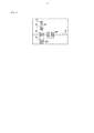
- FIG. 1 shows an equivalent schematic diagram of an impedance matching circuit board of one embodiment of the related art
- Figure 2 is a plan view showing the impedance matching circuit board of the embodiment shown in Figure 1;
- FIG. 3 shows a plan view of a plane partition of an impedance matching circuit board in accordance with one embodiment of the present invention
- FIG. 4 is a plan view showing a planar division of an impedance matching circuit board in accordance with another embodiment of the present invention.
- Figure 5 is a plan view showing a first embodiment of an impedance matching circuit board according to the present invention.
- FIG. 6 is a plan view showing a second embodiment of an impedance matching circuit board according to the present invention.
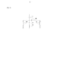
- Figure 7 shows an equivalent schematic view of a third embodiment of an impedance matching circuit board in accordance with the present invention.
- FIG. 8 is a plan view showing a first embodiment of the impedance matching circuit board shown in FIG. 7;
- FIG. 9 is a plan view showing a second embodiment of the impedance matching circuit board shown in FIG.
- FIG. 1 shows an equivalent schematic diagram of an impedance matching circuit board of one embodiment of the related art.
- FIG. 2 is a plan view showing the impedance matching circuit board of the embodiment shown in FIG. 1.
- the transmission line 102 of the lumped component line can be equivalent to the first impedance 102A and the second impedance 102B, and the specified lumped element Z and capacitor 106A are used as the L-type filter circuit, and the capacitor The 106A is attached to the 106 position, and the designated lumped element Z is attached between the common pad 108 and the second pad 112.
- FIG. 3 shows a planar partitioning diagram of an impedance matching circuit board in accordance with one embodiment of the present invention.
- FIG. 4 is a diagram showing a planar partitioning of an impedance matching circuit board in accordance with another embodiment of the present invention.
- Figure 5 is a plan view showing a first embodiment of an impedance matching circuit board in accordance with the present invention.
- Figure 6 is a plan view showing a second embodiment of an impedance matching circuit board in accordance with the present invention.
- Fig. 7 shows an equivalent schematic view of a third embodiment of an impedance matching circuit board in accordance with the present invention.
- FIG. 8 is a plan view showing a first embodiment of the impedance matching circuit board shown in FIG.
- FIG. 9 is a plan view showing a second embodiment of the impedance matching circuit board shown in FIG.
- the impedance matching circuit board according to an embodiment of the present invention will be specifically described below with reference to FIGS. 3 to 9.
- an impedance matching circuit board includes: a microstrip line 104, a short circuit connected to a specified component in a lumped element line, or an open circuit disposed at a periphery of a specified component,
- the reactance value of the microstrip line 104 is determined by the operating frequency of the electromagnetic signal, wherein the lumped component line is provided with a common pad 108 for simultaneously soldering a plurality of specified components One pin.
- the transmission line 102 having an end characteristic impedance of Z 0 has a purely reactive input impedance Z in if the length of the transmission line 102 is And the corresponding working frequency .
- the electrical length of the transmission line 102 is a geometric length Its electromagnetic wave wavelength
- the ratio of the line width of the microstrip line 104 and the substrate parameters determine the characteristic impedance of the transmission line 102.
- the line length of the microstrip line 104 and the substrate parameter frequency determine the electrical length of the transmission line 102.
- the specifying component includes at least one of a capacitor 106A, an inductor, and a resistor connected in parallel and/or in series in the lumped component line.
- the electromagnetic wave is subjected to filtering processing by providing at least one of the capacitor 106A, the inductance and the resistance connected in parallel and/or in series in the lumped element line.
- the lumped element line when the lumped element line is an L-type filter circuit, the lumped element line includes: a capacitor 106A (welded to two pads in the region 106) connected to the L-type filter circuit.
- the input pad is connected between the output line and the output line; the first pad 110 and the second pad 112 are respectively disposed on two sides of the common pad 108, and the common pad 108 is disposed on the input line or the output end.
- a wire wherein the first pad 110 and the common pad 108 are used to solder the first resistor or the first inductor or the first capacitor 116A, and the second pad 112 and the common pad 108 are used to solder the second resistor or the second inductor Or the second capacitor 118A.
- Embodiment 1 is a diagrammatic representation of Embodiment 1:
- a first resistor or a first inductor or a first capacitor 116A (soldering region 116) is soldered between the first pad 110 and the common pad 108, and the second pad 112 is empty.
- the lumped element line further includes a third pad 114 disposed on a side of the first pad 110 away from the common pad 108, and a microstrip line 104 soldered between the first pad 110 and the third pad 114. .
- Embodiment 2 is a diagrammatic representation of Embodiment 1:
- a second resistor or a second inductor or a second capacitor 118A (welding region 118) is soldered between the second pad 112 and the common pad 108, and the lumped component line further includes The third pad 114 is disposed on a side of the first pad 110 away from the common pad 108, and the microstrip line 104 is soldered between the first pad 110 and the third pad 114.
- Embodiment 3 is a diagrammatic representation of Embodiment 3
- the L-type filter circuit includes a first inductor L11, a second inductor L12, and equivalent resistances 102A and 102B of the transmission line.
- the capacitor 106A is used for filtering DC interference, and the microstrip line 104 is shorted to the second.
- the L-type filter circuit includes a first capacitor C11, a second capacitor C12, and equivalent resistances 102A and 102B of the transmission line.
- the capacitor 106A is used for filtering DC interference, and the microstrip line 104 is shorted to the second. Inductor C12.
- a first resistor or a first inductor or a first capacitor 116A (solder region 116) is soldered between the first pad 110 and the common pad 108, and the second pad 112 and A second resistor or a second inductor or a second capacitor 118A (soldering region 118) is soldered between the common pads 108.
- the lumped component line further includes: a third pad 114 disposed on the first pad 110 away from the common pad. On one side of the 108, a microstrip line 104 is soldered between the first pad 110 and the third pad 114.
- the transmission line 102 of the lumped element line is a coaxial line, wherein the characteristic impedance of the coaxial line is 50 ohms or 75 ohms.
- the reactance of the microstrip line 104 is less than 0.6 nH.
- the reactance of the microstrip line 104 to less than 0.6 nH, such as 0.1 nH, 0.2 nH, or even 0.05 nH, etc., for the high frequency band of the electromagnetic wave, often the dispersion of the discrete value is large, resulting in a performance index critical.
- the production rate of the production line is high, the defect rate is high, and the current 5G protocol is promoted, but the higher the transmission frequency, the worse the lumped component performance, and the smaller the transmission line 102 size, the accuracy of the transmission line 102 within 10G can be ignored relative to the lumped component.
- the subsequent radio frequency may gradually transition to the transmission line 102, and the following technical problem is optimized: the common end matching of the duplexer cannot be adjusted and converged, that is, the transmitted ACLR (Adjacent Channel Leakage Ratio) is not flat or not up to standard, and the sensitivity is The indicator is not flat or not up to standard.
- the transmitted ACLR Adjacent Channel Leakage Ratio
- the present invention proposes a new impedance matching circuit board by using a microstrip line ( Or called a stub line) is set in the lumped component line, which improves the dispersion and reliability of the RF circuit, and solves the high cost problem of the lumped component with a small reactance value.
- a microstrip line Or called a stub line
Landscapes
- Engineering & Computer Science (AREA)
- Microelectronics & Electronic Packaging (AREA)
- Control Of Motors That Do Not Use Commutators (AREA)
- Circuit Arrangements For Discharge Lamps (AREA)
Abstract
一种阻抗匹配电路板、天线和终端,其中,阻抗匹配电路板包括:微带线(104)短路连接至所述集总元件线路中的指定元件,或开路设于所述指定元件的周部,用于与所述指定元件进行阻抗匹配,所述微带线(104)的电抗值由所述电磁信号的工作频率确定,其中,所述集总元件线路中设有共用焊盘(108),所述共用焊盘(108)用于同时焊接多个指定元件的一个引脚。该方案提高了阻抗电路的匹配度和元件离散性。
Description
本申请要求于2016年9月23日提交中国专利局,申请号为201610846918.7、发明名称为“阻抗匹配电路板、天线和终端”的中国专利申请的优先权,其全部内容通过引用结合在本申请中。
本发明涉及射频技术领域,具体而言,涉及一种阻抗匹配电路板、一种天线和一种终端。
在射频电路的相关技术中,L型滤波电路作为一种主流的阻抗匹配电路包括两个以上的集总元件,常见的集总元件包括电容、电感和电阻等,由于实际情况下,集总元件的电抗值是不连续的,如电感值有0.6nH、0.9nH、1nH、1.2nH、1.3nH、1.5nH、1.8nH、2nH、2.2nH、2.4nH、2.7nH、2.9nH、3nH、3.3nH……18nH、27nH、33nH……。
基于常见的集总元件实现阻抗匹配至少存在以下技术缺陷:
(1)由于集总元件的电抗值较为离散,因此,射频工程师处于工艺成本考虑,例如,没有小于0.6nH的电感,难以实现精确的阻抗匹配;
(2)如果电抗值较小的集总元件被商业垄断,会提高产品的成本,例如终端厂商需支付高额的专利产品的使用费用,无形中提高终端产品的价格。
本发明正是基于上述技术问题至少之一,提出了一种新的阻抗匹配电路板,通过将微带线(或称作短截线)设于集总元件线路中,提高了射频电路的离散度和可靠性,解决了电抗值较小的集总元件的高成本问题。
有鉴于此,根据本发明的第一方面的实施例,提出了一种阻抗匹配电路板,包括:微带线,短路连接至集总元件线路中的指定元件,或开路设于指定元件的周部,用于与指定元件进行阻抗匹配,微带线的电抗值由电磁信号的工作频率确定,其中,集总元件线路中设有共用焊盘,共用焊盘用于同时焊接多个指定元件的一个引脚。
在该技术方案中,通过将微带线(或称作短截线)设于集总元件线路中,提高了射频电路的离散度和可靠性,解决了电抗值较小的集总元件的高成本问题。
为了将集总元件变化为分布参数元件,需要借助于Richards公式进行计算,如下:


上述公式(1)至(4)中,一端特性阻抗为Z0的传输线具有纯电抗性输入阻抗Zin,如果传输线的长度为 ,而相应的工作频率
 ,
, 为传输线的相速度,则电长度
 可根据公式(2)确定,
 即为Richards变换,电容性集总元件可以用一段开路传输线实现(如公式(4)所示),也即基于Richards变换可以实现用特性阻抗Z0=L的一段短路传输线替代集总参数电感,也可以用特性阻抗Z0=1/C的一端开路传输线替代集总参数电容,可以选用传输线的长度为
 ,但并不是必须的。
其中,传输线的电长度为几何长度 与其电磁波波长
 的比值,微带线的线宽和基板参数决定其传输线的特性阻抗,微带线的线长和基板参数频率决定传输线的电长度
 ,每一条射频发射和接受频段路径一旦确定,其每条传输线的工作频率也就确定了,因此,可以根据工作频率确定微带线的线宽和线长。
例如,特性阻抗为120Ω,电长度为88°,频率为2.5GHz的短路微带线,其simith圆图的电阻接近50Ω,其电抗为0.727,在2.5GHz左右换算电感为L=0.28nH。
值得特别指出的是,通过设置共用焊盘,提高了阻抗匹配电路板的兼容性和集成度,电容和电感之间的互换公式如下:
L=-1/(C×(2×π×f)2) (5)
例如,f=2GHz的10pF电容换算为电感值为0.633nH,因此,短路短截线和开路短截线并不一定只和电容或者电感搭配使用。
在上述技术方案中,优选地,指定元件包括:并联和/或串联于集总元件线路中的电容、电感和电阻中的至少一个元件。
在该技术方案中,通过设置并联和/或串联于集总元件线路中的电容、电感和电阻中的至少一个元件,用于对电磁波进行滤波处理。
在上述技术方案中,优选地,集总元件线路为L型滤波电路时,集总元件线路包括:电容,连接于L型滤波电路的输入端走线和输出端走线之间;第一焊盘和第二焊盘,分别设于共用焊盘的两侧,共用焊盘设于输入端走线或输出端走线,其中,第一焊盘和共用焊盘用于焊接第一电阻或第一电感或第一电容,第二焊盘和共用焊盘用于焊接第二电阻或第二电感或第二电容。
在该技术方案中,通过在共用焊盘两侧设置第一焊盘和第二焊盘,克服了相关技术中传输线一侧设置焊盘的缺陷,提高了阻抗匹配电路的设计的灵活性、可调节性和集成度。
在上述技术方案中,优选地,第一焊盘和共用焊盘之间焊接有第一电阻或第一电感或第一电容,第二焊盘空载,集总元件线路还包括:第三焊盘,设于第一焊盘远离共用焊盘的一侧,第一焊盘与第三焊盘之间焊接有微带线。
在上述技术方案中,优选地,第二焊盘和共用焊盘之间焊接有第二电阻或第二电感或第二电容,集总元件线路还包括:第三焊盘,设于第一焊盘远离共用焊盘的一侧,第一焊盘和第三焊盘之间焊接有微带线。
在上述技术方案中,优选地,第一焊盘和共用焊盘之间焊接有第一电阻或第一电感或第一电容,第二焊盘和共用焊盘之间焊接有第二电阻或第二电感或第二电容,集总元件线路还包括:第三焊盘,设于第一焊盘远离共用焊盘的一侧,第一焊盘与第三焊盘之间焊接有微带线。
在上述技术方案中,优选地,集总元件线路的传输线为同轴线,其中,同轴线的特性阻抗为50欧姆或75欧姆。
在上述技术方案中,优选地,微带线的电抗小于0.6nH。
在该技术方案中,通过设置微带线的电抗小于0.6nH,比如0.1nH,0.2nH,甚至0.05nH等,对于电磁波的高频频段,经常由于离散值跨度较大,导致性能指标临界,从而导致产线批量生产时,次品率高,目前5G协议推广,但是传输频率越高,集总元件性能越差,而传输线尺寸越小,10G以内传输线精度相对于集总元件可以忽略,后续射频可能渐渐向传输线过渡,优化了以下技术问题:双工器的公共端匹配无法调节收敛,即发射的ACLR不平坦或不达标,灵敏度指标不平坦或不达标。
根据本发明的第二方面的实施例,还提出了一种天线,包括如上述任一项技术方案所述的阻抗匹配电路板,因此,该终端具有和上述技术方案中任一项所述的阻抗匹配电路板相同的技术效果,在此不再赘述。
根据本发明的第三方面,还提出了一种终端,包括如上述任一项技术方案所述的天线和阻抗匹配电路板,因此,该终端具有和上述技术方案中任一项所述的天线和阻抗匹配电路板相同的技术效果,在此不再赘述。
通过以上技术方案,通过将微带线(或称作短截线)设于集总元件线路中,提高了射频电路的离散度和可靠性,解决了电抗值较小的集总元件的高成本问题。
图1示出了相关技术的一个实施例的阻抗匹配电路板的等效示意图;
图2示出了图1所示的实施例的阻抗匹配电路板的平面示意图;
图3示出了根据本发明的一个实施例的阻抗匹配电路板的平面分区示意图;
图4示出了根据本发明的另一个实施例的阻抗匹配电路板的平面分区示意图;
图5示出了根据本发明的阻抗匹配电路板的实施例一的平面示意图;
图6示出了根据本发明的阻抗匹配电路板的实施例二的平面示意图;
图7示出了根据本发明的阻抗匹配电路板的实施例三的等效示意图;
图8示出了图7所示的阻抗匹配电路板的实施方式一的平面示意图;
图9示出了图7所示的阻抗匹配电路板的实施方式二的平面示意图。
为了能够更清楚地理解本发明的上述目的、特征和优点,下面结合附图和具体实施方式对本发明进行进一步的详细描述。需要说明的是,在不冲突的情况下,本申请的实施例及实施例中的特征可以相互组合。
在下面的描述中阐述了很多具体细节以便于充分理解本发明,但是,本发明还可以采用第三方不同于在此描述的第三方方式来实施,因此,本发明的保护范围并不受下面公开的具体实施例的限制。
图1示出了相关技术的一个实施例的阻抗匹配电路板的等效示意图。
图2示出了图1所示的实施例的阻抗匹配电路板的平面示意图。
如图1和图2所示,相关技术中,集总元件线路的传输线102可等效为第一阻抗102A和第二阻抗102B,指定的集总元件Z和电容106A作为L型滤波电路,电容106A贴于106位置,指定的集总元件Z贴于共用焊盘108和第二焊盘112之间。
图3示出了根据本发明的一个实施例的阻抗匹配电路板的平面分区示意图。
图4示出了根据本发明的另一个实施例的阻抗匹配电路板的平面分区示意图。
图5示出了根据本发明的阻抗匹配电路板的实施例一的平面示意图。
图6示出了根据本发明的阻抗匹配电路板的实施例二的平面示意图。
图7示出了根据本发明的阻抗匹配电路板的实施例三的等效示意图。
图8示出了图7所示的阻抗匹配电路板的实施方式一的平面示意图。
图9示出了图7所示的阻抗匹配电路板的实施方式二的平面示意图。
下面集合图3至图9对根据本发明的实施例的阻抗匹配电路板进行具体说明。
如图3至图9所示,根据本发明的实施例的阻抗匹配电路板,包括:微带线104,短路连接至集总元件线路中的指定元件,或开路设于指定元件的周部,用于与指定元件进行阻抗匹配,微带线104的电抗值由电磁信号的工作频率确定,其中,集总元件线路中设有共用焊盘108,共用焊盘108用于同时焊接多个指定元件的一个引脚。
在该技术方案中,通过将微带线104(或称作短截线)设于集总元件线路中,提高了射频电路的离散度和可靠性,解决了电抗值较小的集总元件的高成本问题。
为了将集总元件变化为分布参数元件,需要借助于Richards公式进行计算,如下:


上述公式(1)至(4)中,一端特性阻抗为Z0的传输线102具有纯电抗性输入阻抗Zin,如果传输线102的长度为 ,而相应的工作频率
 ,
, 为传输线102的相速度,则电长度
 可根据公式(2)确定,
 即为Richards变换,电容106A性集总元件可以用一段开路传输线102实现(如公式(4)所示),也即基于Richards变换可以实现用特性阻抗Z0=L的一段短路传输线102替代集总参数电感,也可以用特性阻抗Z0=1/C的一端开路传输线102替代集总参数电容106A,可以选用传输线102的长度为
 ,但并不是必须的。
其中,传输线102的电长度为几何长度 与其电磁波波长
 的比值,微带线104的线宽和基板参数决定其传输线102的特性阻抗,微带线104的线长和基板参数频率决定传输线102的电长度
 ,每一条射频发射和接受频段路径一旦确定,其每条传输线102的工作频率也就确定了,因此,可以根据工作频率确定微带线104的线宽和线长。
例如,特性阻抗为120Ω,电长度为88°,频率为2.5GHz的短路微带线104,其simith圆图的电阻接近50Ω,其电抗为0.727,在2.5GHz左右换算电感为L=0.28nH。
值得特别指出的是,通过设置共用焊盘108,提高了阻抗匹配电路板的兼容性和集成度,电容106A和电感之间的互换公式如下:
L=-1/(C×(2×π×f)2) (5)
例如,f=2GHz的10pF电容106A换算为电感值为0.633nH,因此,短路短截线和开路短截线并不一定只和电容106A或者电感搭配使用。
在上述技术方案中,优选地,指定元件包括:并联和/或串联于集总元件线路中的电容106A、电感和电阻中的至少一个元件。
在该技术方案中,通过设置并联和/或串联于集总元件线路中的电容106A、电感和电阻中的至少一个元件,用于对电磁波进行滤波处理。
如图3至图6所示,优选地,集总元件线路为L型滤波电路时,集总元件线路包括:电容106A(焊接于区域106内的两个焊盘),连接于L型滤波电路的输入端走线和输出端走线之间;第一焊盘110和第二焊盘112,分别设于共用焊盘108的两侧,共用焊盘108设于输入端走线或输出端走线,其中,第一焊盘110和共用焊盘108用于焊接第一电阻或第一电感或第一电容116A,第二焊盘112和共用焊盘108用于焊接第二电阻或第二电感或第二电容118A。
在该技术方案中,通过在共用焊盘108两侧设置第一焊盘110和第二焊盘112,克服了相关技术中传输线102一侧设置焊盘的缺陷,提高了阻抗匹配电路的设计的灵活性、可调节性和集成度。
实施例一:
如图4和图5所示,优选地,第一焊盘110和共用焊盘108之间焊接有第一电阻或第一电感或第一电容116A(焊接区域116),第二焊盘112空载,集总元件线路还包括:第三焊盘114,设于第一焊盘110远离共用焊盘108的一侧,第一焊盘110与第三焊盘114之间焊接有微带线104。
实施例二:
如图4和图6所示,优选地,第二焊盘112和共用焊盘108之间焊接有第二电阻或第二电感或第二电容118A(焊接区域118),集总元件线路还包括:第三焊盘114,设于第一焊盘110远离共用焊盘108的一侧,第一焊盘110和第三焊盘114之间焊接有微带线104。
实施例三:
如图7所示,L型滤波电路包括并联的第一电感L11、第二电感L12、传输线的等效电阻102A和102B,电容106A用于滤除直流干扰,微带线104短接至第二电感L12。
如图8所示,L型滤波电路包括并联的第一电容C11、第二电容C12、传输线的等效电阻102A和102B,电容106A用于滤除直流干扰,微带线104短接至第二电感C12。
如图4至图9所示,优选地,第一焊盘110和共用焊盘108之间焊接有第一电阻或第一电感或第一电容116A(焊接区域116),第二焊盘112和共用焊盘108之间焊接有第二电阻或第二电感或第二电容118A(焊接区域118),集总元件线路还包括:第三焊盘114,设于第一焊盘110远离共用焊盘108的一侧,第一焊盘110与第三焊盘114之间焊接有微带线104。
在上述技术方案中,优选地,集总元件线路的传输线102为同轴线,其中,同轴线的特性阻抗为50欧姆或75欧姆。
在上述技术方案中,优选地,微带线104的电抗小于0.6nH。
在该技术方案中,通过设置微带线104的电抗小于0.6nH,比如0.1nH,0.2nH,甚至0.05nH等,对于电磁波的高频频段,经常由于离散值跨度较大,导致性能指标临界,从而导致产线批量生产时,次品率高,目前5G协议推广,但是传输频率越高,集总元件性能越差,而传输线102尺寸越小,10G以内传输线102精度相对于集总元件可以忽略,后续射频可能渐渐向传输线102过渡,优化了以下技术问题:双工器的公共端匹配无法调节收敛,即发射的ACLR(Adjacent Channel Leakage Ratio,邻道泄漏功率比)不平坦或不达标,灵敏度指标不平坦或不达标。
以上结合附图详细说明了本发明的技术方案,考虑到相关技术中如何提高阻抗匹配电路板的离散型的技术问题,本发明提出了一种新的阻抗匹配电路板,通过将微带线(或称作短截线)设于集总元件线路中,提高了射频电路的离散度和可靠性,解决了电抗值较小的集总元件的高成本问题。
以上仅为本发明的优选实施例而已,并不用于限制本发明,对于本领域的技术人员来说,本发明可以有各种更改和变化。凡在本发明的精神和原则之内,所作的任何修改、等同替换、改进等,均应包含在本发明的保护范围之内。
Claims (10)
- 一种阻抗匹配电路板,所述阻抗匹配电路板包括基板和集总元件线路,所述集总元件线路设于所述基板上,用于收发电磁信号,其特征在于,所述阻抗匹配电路板还包括:微带线,短路连接至所述集总元件线路中的指定元件,或开路设于所述指定元件的周部,用于与所述指定元件进行阻抗匹配,所述微带线的电抗值由所述电磁信号的工作频率确定,其中,所述集总元件线路中设有共用焊盘,所述共用焊盘用于同时焊接多个指定元件的一个引脚。
- 根据权利要求1所述的阻抗匹配电路板,其特征在于,所述指定元件包括:并联和/或串联于所述集总元件线路中的电容、电感和电阻中的至少一个元件。
- 根据权利要求1所述的阻抗匹配电路板,其特征在于,所述集总元件线路为L型滤波电路时,所述集总元件线路包括:电容,连接于所述L型滤波电路的输入端走线和输出端走线之间;第一焊盘和第二焊盘,分别设于所述共用焊盘的两侧,所述共用焊盘设于所述输入端走线或所述输出端走线,其中,所述第一焊盘和所述共用焊盘用于焊接第一电阻或第一电感或第一电容,所述第二焊盘和所述共用焊盘用于焊接第二电阻或第二电感或第二电容。
- 根据权利要求3所述的阻抗匹配电路板,其特征在于,所述第一焊盘和所述共用焊盘之间焊接有所述第一电阻或所述第一电感或所述第一电容,所述第二焊盘空载,所述集总元件线路还包括:第三焊盘,设于所述第一焊盘远离所述共用焊盘的一侧,所述第一焊盘与所述第三焊盘之间焊接有所述微带线。
- 根据权利要求3所述的阻抗匹配电路板,其特征在于,所述第二焊盘和所述共用焊盘之间焊接有所述第二电阻或所述第二电感或所述第二电容,所述集总元件线路还包括:第三焊盘,设于所述第一焊盘远离所述共用焊盘的一侧,所述第一焊盘和所述第三焊盘之间焊接有所述微带线。
- 根据权利要求3所述的阻抗匹配电路板,其特征在于,所述第一焊盘和所述共用焊盘之间焊接有所述第一电阻或所述第一电感或所述第一电容,所述第二焊盘和所述共用焊盘之间焊接有所述第二电阻或所述第二电感或所述第二电容,所述集总元件线路还包括:第三焊盘,设于所述第一焊盘远离所述共用焊盘的一侧,所述第一焊盘与所述第三焊盘之间焊接有所述微带线。
- 根据权利要求1至6中任一项所述的阻抗匹配电路板,其特征在于,所述集总元件线路的传输线为同轴线,其中,所述同轴线的特性阻抗为50欧姆或75欧姆。
- 根据权利要求1至6中任一项所述的阻抗匹配电路板,其特征在于,所述微带线的电抗小于0.6nH。
- 一种天线,其特征在于,包括:如权利要求1至8中任一项所述的阻抗匹配电路板。
- 一种终端,其特征在于,包括:如权利要求9所述的天线或如权利要求1至8中任一项所述的阻抗匹配电路板。
Applications Claiming Priority (2)
| Application Number | Priority Date | Filing Date | Title |
|---|---|---|---|
| CN201610846918.7A CN107872919A (zh) | 2016-09-23 | 2016-09-23 | 阻抗匹配电路板、天线和终端 |
| CN201610846918.7 | 2016-09-23 |
Publications (1)
| Publication Number | Publication Date |
|---|---|
| WO2018053933A1 true WO2018053933A1 (zh) | 2018-03-29 |
Family
ID=61690717
Family Applications (1)
| Application Number | Title | Priority Date | Filing Date |
|---|---|---|---|
| PCT/CN2016/107999 Ceased WO2018053933A1 (zh) | 2016-09-23 | 2016-11-30 | 阻抗匹配电路板、天线和终端 |
Country Status (2)
| Country | Link |
|---|---|
| CN (1) | CN107872919A (zh) |
| WO (1) | WO2018053933A1 (zh) |
Families Citing this family (8)
| Publication number | Priority date | Publication date | Assignee | Title |
|---|---|---|---|---|
| CN109587943A (zh) * | 2018-11-09 | 2019-04-05 | 加弘科技咨询(上海)有限公司 | 差分线零桩线共铺走线电路板及电子器件 |
| KR102176860B1 (ko) * | 2019-01-22 | 2020-11-10 | 동우 화인켐 주식회사 | 안테나 구조체 및 이를 포함하는 디스플레이 장치 |
| JP2022518481A (ja) | 2019-01-22 | 2022-03-15 | 東友ファインケム株式会社 | アンテナ構造体及びそれを含むディスプレイ装置 |
| CN110167261B (zh) | 2019-06-26 | 2024-11-05 | 京信网络系统股份有限公司 | 毫米波有源天线单元及pcb板间互连结构 |
| CN113078915B (zh) * | 2019-12-18 | 2023-04-14 | 大富科技(安徽)股份有限公司 | 一种通信设备及其可控阻抗匹配电路 |
| CN112490661B (zh) * | 2020-11-23 | 2021-09-21 | 上海海积信息科技股份有限公司 | 一种阻抗匹配装置及天线 |
| CN114126230B (zh) * | 2021-11-26 | 2024-02-09 | 浪潮电子信息产业股份有限公司 | 一种pcb板的兼容布线方法及相关装置 |
| US12068554B2 (en) * | 2022-01-28 | 2024-08-20 | Hewlett Packard Enterprise Development Lp | Dual-path high-speed interconnect PCB layout solution |
Citations (4)
| Publication number | Priority date | Publication date | Assignee | Title |
|---|---|---|---|---|
| CN101202369A (zh) * | 2007-12-11 | 2008-06-18 | 中国电子科技集团公司第五十五研究所 | 一种小型化mems开关线移相器 |
| CN102110900A (zh) * | 2010-12-27 | 2011-06-29 | 中兴通讯股份有限公司 | 一种移动终端的阵列天线及其实现方法 |
| CN102544675A (zh) * | 2012-01-13 | 2012-07-04 | 重庆邮电大学 | 一种双频不等分功分器 |
| CN105242125A (zh) * | 2014-07-08 | 2016-01-13 | 苏州普源精电科技有限公司 | 具有微带线细调电感的射频测量装置及微带线细调电感 |
Family Cites Families (3)
| Publication number | Priority date | Publication date | Assignee | Title |
|---|---|---|---|---|
| US5511238A (en) * | 1987-06-26 | 1996-04-23 | Texas Instruments Incorporated | Monolithic microwave transmitter/receiver |
| CN1972075A (zh) * | 2006-12-06 | 2007-05-30 | 中国科学院电工研究所 | 一种接收整流天线 |
| CN105242109B (zh) * | 2014-07-08 | 2019-12-13 | 苏州普源精电科技有限公司 | 具有微带线粗调电感的射频测量装置及微带线粗调电感 |
-
2016
- 2016-09-23 CN CN201610846918.7A patent/CN107872919A/zh active Pending
- 2016-11-30 WO PCT/CN2016/107999 patent/WO2018053933A1/zh not_active Ceased
Patent Citations (4)
| Publication number | Priority date | Publication date | Assignee | Title |
|---|---|---|---|---|
| CN101202369A (zh) * | 2007-12-11 | 2008-06-18 | 中国电子科技集团公司第五十五研究所 | 一种小型化mems开关线移相器 |
| CN102110900A (zh) * | 2010-12-27 | 2011-06-29 | 中兴通讯股份有限公司 | 一种移动终端的阵列天线及其实现方法 |
| CN102544675A (zh) * | 2012-01-13 | 2012-07-04 | 重庆邮电大学 | 一种双频不等分功分器 |
| CN105242125A (zh) * | 2014-07-08 | 2016-01-13 | 苏州普源精电科技有限公司 | 具有微带线细调电感的射频测量装置及微带线细调电感 |
Also Published As
| Publication number | Publication date |
|---|---|
| CN107872919A (zh) | 2018-04-03 |
Similar Documents
| Publication | Publication Date | Title |
|---|---|---|
| WO2018053933A1 (zh) | 阻抗匹配电路板、天线和终端 | |
| CN107395148A (zh) | 一种tr组件的温补均衡电路 | |
| WO2016033890A1 (zh) | 一种采用两路反相滤波电路的ltcc滤波巴伦 | |
| CN218124668U (zh) | 射频前端模组 | |
| CN111477999A (zh) | 阶梯阻抗耦合双模谐振器的ipd毫米波带通滤波器芯片 | |
| CN101621150A (zh) | P波段三倍频程微型定向耦合器 | |
| CN111239578A (zh) | 功率管测试夹具及其制备方法 | |
| CN107293835A (zh) | 单节威尔金森功分器 | |
| CN113114152A (zh) | 基于薄膜ipd技术的功分电路、功分器以及电子设备 | |
| US10147698B2 (en) | Radio frequency (RF) devices | |
| CN112563712A (zh) | 一种具有谐波抑制功能的端接复阻抗定向耦合器及设计方法 | |
| CN208015692U (zh) | 一种sir型悬置线滤波器的滤波功率放大器 | |
| CN214900816U (zh) | 基于薄膜ipd技术的功分电路、功分器以及电子设备 | |
| CN112952331B (zh) | 一种小型化平衡-不平衡滤波功分器 | |
| CN113013569B (zh) | 一种输出相位差连续可调的双频带微带混合电桥 | |
| CN110247146A (zh) | 一种基于薄膜集成无源元件技术的宽带功率分配器芯片 | |
| CN110380168A (zh) | 非平衡到平衡的双宽带功分滤波器 | |
| WO2009142457A2 (ko) | 임피던스 매칭 칩 및 이를 이용한 알에프 송수신부 및 알에프 신호전달부 | |
| CN115084816B (zh) | 射频电路、无源电路及电子设备 | |
| CN112583373A (zh) | 一种具有频率相关复数源和负载的带通滤波器芯片 | |
| CN116436427A (zh) | 一种基于过孔电感的数字可重构滤波器 | |
| CN206461078U (zh) | 2‑6GHz、陶瓷基的大功率兰格耦合器 | |
| WO2020116715A1 (ko) | 소형 저손실 밀리미터파 전력 분배 결합 장치 | |
| CN113328226B (zh) | 一种任意功分比的平衡-不平衡耦合器 | |
| CN107293521B (zh) | 实现l波段器件50ω阻抗匹配的方法 |
Legal Events
| Date | Code | Title | Description |
|---|---|---|---|
| 121 | Ep: the epo has been informed by wipo that ep was designated in this application |
Ref document number: 16916672 Country of ref document: EP Kind code of ref document: A1 |
|
| NENP | Non-entry into the national phase |
Ref country code: DE |
|
| 122 | Ep: pct application non-entry in european phase |
Ref document number: 16916672 Country of ref document: EP Kind code of ref document: A1 |