WO2018042817A1 - 撮像装置 - Google Patents
撮像装置 Download PDFInfo
- Publication number
- WO2018042817A1 WO2018042817A1 PCT/JP2017/021970 JP2017021970W WO2018042817A1 WO 2018042817 A1 WO2018042817 A1 WO 2018042817A1 JP 2017021970 W JP2017021970 W JP 2017021970W WO 2018042817 A1 WO2018042817 A1 WO 2018042817A1
- Authority
- WO
- WIPO (PCT)
- Prior art keywords
- imaging
- imaging device
- display
- image
- display unit
- Prior art date
- Legal status (The legal status is an assumption and is not a legal conclusion. Google has not performed a legal analysis and makes no representation as to the accuracy of the status listed.)
- Ceased
Links
Images







Classifications
-
- G—PHYSICS
- G03—PHOTOGRAPHY; CINEMATOGRAPHY; ANALOGOUS TECHNIQUES USING WAVES OTHER THAN OPTICAL WAVES; ELECTROGRAPHY; HOLOGRAPHY
- G03B—APPARATUS OR ARRANGEMENTS FOR TAKING PHOTOGRAPHS OR FOR PROJECTING OR VIEWING THEM; APPARATUS OR ARRANGEMENTS EMPLOYING ANALOGOUS TECHNIQUES USING WAVES OTHER THAN OPTICAL WAVES; ACCESSORIES THEREFOR
- G03B15/00—Special procedures for taking photographs; Apparatus therefor
-
- G—PHYSICS
- G03—PHOTOGRAPHY; CINEMATOGRAPHY; ANALOGOUS TECHNIQUES USING WAVES OTHER THAN OPTICAL WAVES; ELECTROGRAPHY; HOLOGRAPHY
- G03B—APPARATUS OR ARRANGEMENTS FOR TAKING PHOTOGRAPHS OR FOR PROJECTING OR VIEWING THEM; APPARATUS OR ARRANGEMENTS EMPLOYING ANALOGOUS TECHNIQUES USING WAVES OTHER THAN OPTICAL WAVES; ACCESSORIES THEREFOR
- G03B19/00—Cameras
- G03B19/02—Still-picture cameras
- G03B19/04—Roll-film cameras
- G03B19/07—Roll-film cameras having more than one objective
-
- G—PHYSICS
- G09—EDUCATION; CRYPTOGRAPHY; DISPLAY; ADVERTISING; SEALS
- G09F—DISPLAYING; ADVERTISING; SIGNS; LABELS OR NAME-PLATES; SEALS
- G09F9/00—Indicating arrangements for variable information in which the information is built-up on a support by selection or combination of individual elements
- G09F9/30—Indicating arrangements for variable information in which the information is built-up on a support by selection or combination of individual elements in which the desired character or characters are formed by combining individual elements
-
- H—ELECTRICITY
- H04—ELECTRIC COMMUNICATION TECHNIQUE
- H04N—PICTORIAL COMMUNICATION, e.g. TELEVISION
- H04N23/00—Cameras or camera modules comprising electronic image sensors; Control thereof
- H04N23/90—Arrangement of cameras or camera modules, e.g. multiple cameras in TV studios or sports stadiums
-
- H—ELECTRICITY
- H04—ELECTRIC COMMUNICATION TECHNIQUE
- H04N—PICTORIAL COMMUNICATION, e.g. TELEVISION
- H04N7/00—Television systems
- H04N7/14—Systems for two-way working
Definitions
- the present disclosure relates to an imaging apparatus.
- Japanese Patent Laid-Open No. 2004-228561 uses a rod-shaped lens inserted into a hole provided in a display and an imaging element arranged on the back side to capture an image of a user existing on the display surface side from the vicinity of the center of the display.
- An apparatus is disclosed.
- the present disclosure proposes a new and improved imaging apparatus capable of realizing line-of-sight matching corresponding to a wide-angle imaging region and providing a higher quality image.
- a display unit that displays an image and an imaging unit that captures an image
- the display unit includes at least one hole
- the imaging lens of the imaging unit includes the display
- An imaging device is provided, which is disposed on the back side of the display surface of the unit at a position where the display surface side can be imaged through the hole.
- line-of-sight matching corresponding to a wide-angle imaging region can be realized, and a higher-quality image can be provided.
- FIG. 2 is a system configuration example according to the first embodiment of the present disclosure. It is a functional block diagram of the imaging device concerning the embodiment. It is a plane sectional view of the imaging device concerning the embodiment. It is a figure for demonstrating arrangement
- composition of an image sensor which has a plurality of image pick-up fields in the perpendicular direction concerning the embodiment. It is an example of composition of an image pick-up part provided with a plurality of image pick-up lenses in the perpendicular direction concerning the embodiment. It is an example of composition of an imaging device provided with a plurality of image pick-up parts concerning the embodiment. It is a plane sectional view of an imaging device concerning a 3rd embodiment of this indication. It is a plane sectional view of an imaging device concerning a 4th embodiment of this indication. It is a figure which shows the structure outline
- summary of the imaging device which concerns on 5th Embodiment of this indication. 2 is a hardware configuration example of an imaging apparatus according to the present disclosure.
- the imaging device enables the user's line of sight to be matched in an imaging / display system using a large display device.
- the imaging apparatus can reduce black float and provide a higher quality image.
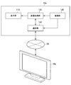
- FIG. 1 is a diagram illustrating a system configuration example of the present embodiment.
- FIG. 1 shows an example in which bidirectional communication is realized using the imaging apparatus according to the present embodiment. That is, FIG. 1 shows an example in which the imaging apparatus according to the present embodiment is used for a video phone, a video conference system, or the like.
- the imaging / display system includes a plurality of imaging devices 10a and 10b.
- the plurality of imaging devices 10a and 10b are connected via the network 20 so that they can communicate with each other.
- the imaging device 10 can be realized by various devices having an imaging function and a display function.
- the imaging device 10 a captures an image including the user P ⁇ b> 1 and transmits the image to the imaging device 10 b via the network 20.
- the imaging device 10a acquires an image including the user P2 captured by the imaging device 10b, and provides the image to the user P1.
- the imaging device 10b captures an image including the user P2, and transmits the image to the imaging device 10a via the network 20. Further, the imaging device 10b acquires an image including the user P1 captured by the imaging device 10a and provides the image to the user P2.
- the imaging devices 10a and 10b according to the present embodiment can match the lines of sight of the users P1 and P2.
- the imaging device 10 according to the present embodiment includes a display unit having a hole and an imaging unit that captures an image.
- one of the characteristics is that the imaging lens of the imaging unit is arranged in a range in which the display surface side can be imaged through a hole on the back side of the display surface of the display surface. Details of the above configuration will be described separately in detail.
- the network 20 has a function of connecting a plurality of imaging devices 10a and 10b.
- the network 20 may include a public line network such as the Internet, a telephone line network, a satellite communication network, various LANs (Local Area Network) including Ethernet (registered trademark), a WAN (Wide Area Network), and the like. Further, the network 20 may include a dedicated line network such as an IP-VPN (Internet Protocol-Virtual Private Network).
- the network 20 may include a wireless communication network such as Wi-Fi (registered trademark) or Bluetooth (registered trademark).
- the system configuration example in the case where the imaging apparatus 10 according to the present embodiment is used in an imaging / display system related to bidirectional communication has been described.
- the case where the imaging / display system includes two imaging devices 10 a and 10 b is described as an example.
- the number of imaging devices 10 according to the present embodiment is limited to the example.
- the imaging / display system according to the present embodiment may include three or more imaging devices 10.
- the imaging / display system according to the present embodiment may further include a configuration other than that shown in FIG.
- the imaging / display system according to the present embodiment may include an acoustic device or the like that is realized separately from the imaging device 10.
- the system configuration according to the present embodiment can be flexibly modified according to the system specifications, operating conditions, and the like.
- FIG. 2 is a functional block diagram of the imaging apparatus 10 according to the present embodiment.
- the imaging apparatus 10 according to the present embodiment includes a display unit 110, an imaging unit 120, an image processing unit 130, and a communication unit 140.
- a display unit 110 the imaging apparatus 10 according to the present embodiment includes a display unit 110, an imaging unit 120, an image processing unit 130, and a communication unit 140.
- the display unit 110 has a function of displaying an image captured by the imaging unit 120 or the external imaging device 10.
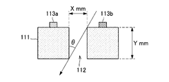
- FIG. 3 is a plan sectional view of the display unit 110.
- the display unit 110 according to the present embodiment includes a light shielding substrate 111, a hole 112, and a plurality of light emitting elements 113a and 113b.
- the light shielding substrate 111 can be realized by a material having a function of absorbing external light from illumination or the like.
- a metal such as Cr may be used for part or all of the light shielding substrate 111.
- the external light absorption function of the light shielding substrate 111 may be realized by applying an organic material system such as a black pigment, for example.
- At least one hole 112 is formed so as to penetrate the light shielding substrate 111.
- the hole 112 according to the present embodiment may be formed at an angle parallel to the perpendicular of the display unit 110 or the light shielding substrate 111.
- the shape of the hole 112 according to the present embodiment may be, for example, a circle including an ellipse, a square, a rectangle, or another polygon.
- the holes 112 according to the present embodiment are formed between pixels or sub-pixels.
- the hole 112 is formed between the sub-pixels. That is, in the example of FIG. 3, the hole 112 is formed between the light emitting elements 113 in the light shielding substrate 111.
- the plurality of light emitting elements 113a and 113b may be realized by, for example, LED (Light Emitting Diode) elements. That is, the display unit 110 according to the present embodiment may be an LED display. In the example illustrated in FIG. 3, external light entering the inside of the imaging device 10 is indicated by an arrow. That is, the light emitting elements 113a and 113b are arranged on the display surface side of the display unit 110.
- LED Light Emitting Diode
- the imaging unit 120 has a function of capturing still images and moving images. For this reason, the imaging unit 120 according to the present embodiment includes an imaging lens 121 and an imaging element 122.
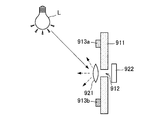
- FIG. 4A is a cross-sectional view of another imaging device 90 different from the imaging device 10 according to the present embodiment when cut in the vertical direction.
- Another imaging device 90 may have the same configuration as the imaging device 10 according to the present embodiment.
- FIG. 4A shows a positional relationship among the light shielding substrate 911, the hole 912, the light emitting elements 913a and 913b, the imaging lens 921, and the imaging element 922 of another imaging apparatus 90.
- the imaging lens 921 is located on the display surface side of the light shielding substrate 911.
- the external light source L and the external light emitted from the external light source L are indicated by straight arrows.
- external light from the external light source L is diffusely reflected by the imaging lens 921.
- the reflected light from the imaging lens 921 is indicated by a dotted arrow.
- the imaging lens 921 diffusely reflects external light from the external light source L, and there is a concern that black floating may occur.
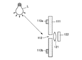
- FIG. 4B is a cross-sectional view of the imaging device 10 according to this embodiment when cut in the vertical direction. 4B shows the positional relationship among the light shielding substrate 111, the hole 112, the light emitting elements 113a and 113b, the imaging lens 121, and the imaging element 122 of the imaging apparatus 10 according to the present embodiment.
- the external light source L and the external light emitted from the external light source L are indicated by straight arrows.
- the imaging lens 121 is located on the back side of the light shielding substrate 111.
- the imaging apparatus 10 according to the present embodiment by arranging the imaging lens 121 on the back side of the display surface of the display unit 110 as described above, it is possible to prevent irregular reflection of external light emitted from the external light source L. is there. That is, according to the imaging device 10 according to the present embodiment, the possibility of black floating can be significantly reduced.
- the imaging lens 121 is arranged on the back side of the hole 112, the arrangement of the imaging lens 121 according to the present embodiment is not limited to such an example.
- One of the features of the imaging lens 121 according to the present embodiment is that the imaging lens 121 is disposed on the back side of the display surface of the display unit 110 at a position where the display surface side can be imaged through the hole 112.
- the imaging lens 121 according to the present embodiment may be arranged such that a part or the whole is inserted into the hole 112. Even in the case of being arranged as described above, the imaging lens 121 according to the present embodiment can prevent irregular reflection of external light emitted from the external light source L.
- the hole 112 and the imaging lens 121 according to the present embodiment are arranged in the vicinity of the center of the light-shielding substrate 111 as in the example illustrated in FIG. 4B, so that the imaging unit is arranged at the edge of the display unit. Compared with the above, it has a high gaze matching effect.
- the image processing unit 130 has a function of controlling display of an image captured by the imaging unit 120 or an external imaging device.
- the image processing unit 130 may cause the display unit 110 to display an image captured by the imaging unit 120 or an external imaging device.
- it has a function of performing various processes on the image captured by the imaging unit 120.
- the image processing unit 130 according to the present embodiment can superimpose and display a virtual object on a subject in an image captured by the imaging unit 120 or an external imaging device.
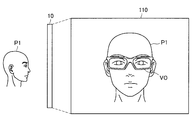
- FIG. 5 is a diagram illustrating an example of virtual object display control by the image processing unit 130.
- the imaging device 10 and the user P1 existing on the display surface side of the imaging device 10 are shown. Further, the display surface of the display unit 110 of the imaging device 10 is shown on the right side of FIG.
- the display unit 110 displays an image including the user P1. That is, the example illustrated in FIG. 5 illustrates a case where an image captured by the imaging unit 120 of the imaging device 10 is displayed on the display unit 110. Referring to FIG. 5, the display unit 110 displays a glasses-type virtual object VO in addition to the image of the user P1.
- the image processing unit 130 according to the present embodiment can superimpose the virtual object on the captured image and cause the display unit 110 to display the virtual object.
- the imaging device 10 according to the present embodiment it is possible to display a virtual object in a superimposed manner while realizing a high line-of-sight matching effect even when the user displays a self-portrait on the display unit 110.
- the user can simulate a product that suits him / her by selecting a virtual object such as glasses to be displayed in a superimposed manner.
- FIG. 5 illustrates an example in which the image processing unit 130 displays the glasses-type virtual object VO, but the virtual object according to the present embodiment is not limited to such an example.
- the virtual object according to the present embodiment may be, for example, various clothes and ornaments, a make-up, a hairstyle, or the like.
- the communication unit 140 has a function of performing information communication with various devices including another imaging device 10 via the network 20.
- the communication unit 140 according to the present embodiment has a function of transmitting an image captured by the imaging unit 120 to another imaging device 10.
- the communication unit 140 has a function of receiving an image captured by another imaging device 10.
- FIG. 3 shows the diameter X of the hole 112 and the thickness Y of the light shielding substrate 111. Also, in FIG. 3, external light entering the inside of the imaging device 10 is indicated by straight arrows.
- the hole 112 may be formed to be parallel to the perpendicular of the light shielding substrate 111.
- FIG. 6 shows a field angle of a general imaging device 920 and an image P captured by the imaging device 920.
- the angle of view can be defined as twice the maximum incident angle ⁇ , that is, 2 ⁇ .
- FIG. 7 shows the result of calculating the relationship between the angle of view 2 ⁇ and the diameter X of the hole 112 based on the above assumption.
- FIG. 7 shows a calculation result when the thickness Y of the light shielding substrate 111 is 0.4 mm.
- the field angle 2 ⁇ is 70 deg.
- the field angle 2 ⁇ is 90 deg. .
- FIG. 8 shows the relationship between the focal length and the angle of view 2 ⁇ of a general imaging device 920 and images taken at each focal length.
- the focal length is 24 mm
- the field angle 2 ⁇ is 84 degrees
- the image Pa is captured.
- the angle of view 2 ⁇ is 45 degrees
- the image Pb can be captured.
- the field angle 2 ⁇ is 34 deg
- the image Pc is captured.
- the angle of view 2 ⁇ is 12 degrees, and it can be seen that the image Pd is captured.
- the imaging apparatus 10 according to the present embodiment can improve the black float and provide a higher quality image while realizing the line-of-sight matching effect corresponding to wide-angle imaging. That is, the imaging device 10 according to the present embodiment is applicable to an imaging / display system including a large display device.
- Second Embodiment> [2.1. Outline of Second Embodiment] Next, an overview of the second embodiment according to the present disclosure will be described.
- the application range of the angle of view of the imaging device 10 has been described with emphasis.
- the imaging apparatus 10 includes a plurality of holes 112 and a plurality of imaging lenses 121, and at least one of the plurality of holes includes a display unit.
- One of the features is that it is formed in an oblique direction with respect to 110 perpendicular lines.
- plays is described.
- FIG. 9 is a diagram for explaining the area opening ratio of the hole 112.
- the area aperture ratio of the hole 112 is defined by the positional relationship between the opening on the display surface side and the opening on the back surface side.
- the actual opening viewed from the incident light is as shown in FIG. It becomes the overlapping part a3 of the opening a2.
- the area aperture ratio of the hole 112 depends on the incident angle ⁇ , the thickness Y of the light shielding substrate 111, and the diameter X of the hole 112.
- the area aperture ratio r when the diameter X of the hole 112 is 0.4 mm, the thickness Y of the light shielding substrate 111 is 0.4 mm, and the incident angle ⁇ is 0 deg. 1 is defined.
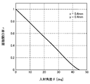
- FIG. 10 shows the relationship between the area aperture ratio r of the hole 112 of the imaging device 10 according to the first embodiment and the incident angle ⁇ based on the above assumption. Referring to FIG. 10, it can be seen that the magnitude of the incident angle ⁇ strongly affects the area aperture ratio r.
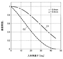
- FIG. 11 is a diagram illustrating a relationship between the area aperture ratio r of the hole 112 of the imaging apparatus 10 according to the first embodiment and the image plane illuminance L based on the cosine fourth law.
- the image plane illuminance L in the general imaging device 920 is indicated by a curve C1
- the image plane illuminance L in the imaging device 10 according to the first embodiment is indicated by a curve C2.
- the image plane illuminance L when the incident angle ⁇ is 0 deg is defined as 1.
- the image plane illuminance L in the imaging apparatus 10 according to the first embodiment has a large decrease in sensitivity as compared with a general imaging apparatus 920, and the incident angle ⁇ is 20 degrees when the incident angle ⁇ is 20 degrees. It can be seen that the value drops to about half that when ⁇ is 0 deg.
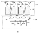
- FIG. 12 is a cross-sectional plan view when the imaging device 10 according to the present embodiment is cut in the horizontal direction.
- the imaging apparatus 10 according to the present embodiment is characterized by including a plurality of holes 112a, 112b, and 112c and a plurality of imaging lenses 121a, 121b, and 121c.
- At least one of the plurality of holes 112a to 112c included in the imaging device 10 according to the present embodiment is formed in an oblique direction with respect to the perpendicular of the display unit 110.
- the example shown in FIG. 12 shows a case where the holes 112 a and 112 c are formed in an oblique direction with respect to the normal of the display unit 110.
- the plurality of holes 112a to 112c and the plurality of imaging lenses 121a to 121c according to the present embodiment may correspond one-to-one.
- the imaging lenses 121 corresponding to the respective holes 112 it is possible to efficiently collect the light incident from the holes 112.
- the imaging unit 120 includes an imaging element 122 having a plurality of imaging surfaces 123a to 123c in a single semiconductor chip. That is, according to the imaging element 122 according to the present embodiment, it is possible to capture a plurality of independent images with a single semiconductor chip. As shown in FIG. 12, a signal readout circuit 124 is disposed between the plurality of imaging surfaces 123a to 123c.
- the plurality of imaging lenses 121a to 121c collects incident light from the holes 112 on the plurality of imaging surfaces 123a to 123c, respectively.
- the incident light from the hole 112a is collected by the imaging lens 121a and forms an image on the imaging surface 123a.
- incident light from the hole 112b is collected by the imaging lens 121b and forms an image on the imaging surface 123b.
- incident light from the hole 112c is collected by the imaging lens 121c and forms an image on the imaging surface 123c.
- the plurality of imaging surfaces 123a to 123c can capture images specialized for incident light from the plurality of holes 112a to 112c, respectively.
- angles of the plurality of holes 112a to 112c according to the present embodiment are formed to increase as the distance from the center of the imaging element 122 of the imaging unit 120 increases.
- the angle ⁇ of the hole 112b closest to the center of the image sensor 122 may be 0 deg.
- the angles ⁇ of the holes 112a and 112c may be ⁇ 30 deg and +30 deg, respectively.
- the angle of the hole 112 is formed based on the relative position with respect to the imaging element 122, so that incident light having a large incident angle ⁇ can be collected more efficiently.
- the incident angle ⁇ is limited to a range of 20 degrees.
- the decrease in the image plane illuminance L is suppressed to 0.42.
- the maximum incident angle of a general imaging device 920 mounted on a portable terminal or the like is up to 35 deg, the decrease in the image plane illuminance L in the imaging device 10 in this embodiment is almost the same as that of the general imaging device 920. It can be seen that it is reduced to the same extent.
- the angle of view 2 ⁇ of the images P1a to P1c respectively acquired by the imaging surfaces 123a to 123c is about 40 deg.
- the image processing unit 130 according to the present embodiment can generate a wide-angle image by connecting the images P1a to P1c by signal processing.
- FIG. 13 shows an example of the composite image Pcom generated by the image processing unit 130 according to the present embodiment.
- the composite image Pcom according to the present embodiment is generated from the images P1a to P1c.
- the images P1a to P1c may be images captured by the imaging surfaces 123a to 123c, respectively.
- the angle of view 2 ⁇ of the images P1a to P1c is 40 degrees.
- the image processing unit 130 according to the present embodiment can perform accurate signal processing by using the overlapping portions of the images P1a and P1b and the images P1b and P1c. At this time, if the overlapping portion is 10 deg, the image processing unit 130 according to the present embodiment can generate a composite image Pcom having a full angle of view of 100 deg. Further, when the overlapping portion is reduced as much as possible, the image processing unit 130 according to the present embodiment can also obtain a composite image Pcom having a total angle of view of about 120 degrees.
- the display unit 110 can display the composite image Pcom generated from the images captured by the plurality of imaging surfaces 123a to 123c. For this reason, according to the imaging device 10 according to the present embodiment, it is possible to provide a higher-quality wide-angle image in which the decrease in image plane illuminance is suppressed.
- either the shape of the center side of the display unit 110 or the shape of the edge side of the display unit 110 related to the hole 112a or the hole 112c shown in FIG. 12 is parallel to the perpendicular of the light shielding substrate 111, for example. It may be formed as follows. When the hole 112a or the hole 112c is formed as described above, more incident light can be collected, and an effect of further suppressing the decrease in the image plane illuminance L is expected.
- the imaging apparatus 10 includes the three holes 112a to 112c, the three imaging lenses 121a to 121c, and the three imaging surfaces 123a to 123c in the horizontal direction has been described.
- the configuration of the imaging apparatus 10 according to the present embodiment is not limited to such an example.
- the imaging device 10 according to the present embodiment may include two combinations of the hole 112, the imaging lens 121, and the imaging surface 123 in the horizontal direction, or may include four or more.
- FIG. 14A is a configuration example of the display unit 110 when the imaging apparatus 10 adopts the above configuration.
- a configuration on the display surface side of the display unit 110 when the imaging device 10 includes a total of nine holes 112a to 112i in three rows in the horizontal direction and three rows in the vertical direction is shown.
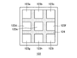
- FIG. 14B shows a configuration example of the imaging element 122 when the imaging device 10 has nine holes 112.
- the imaging element 122 includes nine imaging surfaces 123a to 123i corresponding to the nine holes 112a to 112i.
- a signal readout circuit 124 may be disposed between the nine imaging surfaces 123a to 123i.
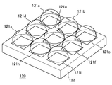
- FIG. 14C is a diagram illustrating a configuration of the imaging unit 120 when the imaging device 10 has nine holes.
- the imaging unit 120 includes nine imaging lenses 121a to 121i corresponding to the nine imaging surfaces 123a to 123i.
- the imaging apparatus 10 includes a plurality of combinations of the hole 112, the imaging lens 121, and the imaging surface 123 not only in the horizontal direction but also in the vertical direction. be able to. According to this configuration, it is possible to obtain a wide-angle image corresponding to the vertical direction in addition to the horizontal direction.
- the imaging apparatus 10 may include a plurality of imaging units 120 as illustrated in FIG. 14C.
- FIG. 15 shows a configuration example when the imaging apparatus 10 includes a plurality of imaging units 120a to 120c.
- FIG. 15 shows the imaging apparatus 10 including a large display unit 110 having a width particularly in the horizontal direction.
- the imaging apparatus 10 may be configured such that a plurality of imaging units 120a to 120c are arranged in the horizontal direction as shown in FIG.
- the imaging device 10 By configuring the imaging device 10 as described above, it is possible to use the imaging unit 120 corresponding to the detected user position, and it is possible to realize line-of-sight matching in a wider range.
- FIG. 16 is a cross-sectional plan view when the imaging device 10 according to the present embodiment is cut in the horizontal direction.
- the display unit 110 according to the present embodiment includes a light shielding substrate 111, a plurality of holes 112a to 112c, a plurality of color filters 114a to 114f, a backlight 115, and a plurality of hole walls 116a to 116c.
- the light-shielding substrate 111 includes glass 111a and 111c, a liquid crystal layer 111b, and a polarizing film 111d.
- incident light can be shielded by the relationship between the orientation and twist of the liquid crystal and the polarization direction of the polarizing film. Therefore, in this embodiment, the liquid crystal display includes the glass 111a and 111c, the liquid crystal layer 111b, and the polarizing film 111d.
- the multilayer structure can be regarded as the light shielding substrate 111.
- the holes 112a to 112c are formed in the liquid crystal layer 111b.
- Corresponding hole walls 116a to 116c are provided around the holes 112a to 112c.
- liquid crystal can be injected between the glasses 111a and 111c by capillary action, and the liquid crystal layer 111b can be generated.
- the polarizing film 111d is disposed so as not to block incident light incident from the holes 112a to 112c.
- the polarizing film 111d is disposed so as not to block incident light incident from the holes 112a to 112c.
- the color filter 114 according to the present embodiment can be regarded as a sub-pixel of the display unit 110.
- the imaging apparatus 10 according to the present embodiment by forming the holes 112 between the color filters 114, it is possible to achieve a line-of-sight matching effect without affecting the image quality of the display unit 110.
- the structural features of the imaging apparatus 10 according to the present embodiment have been described. According to the imaging device 10 according to the present embodiment, even when a liquid crystal display is employed for the display unit 110, the same effects as those of the second embodiment can be achieved.
- the configuration of the imaging unit 120 according to the present embodiment may be substantially the same as the configuration of the imaging unit 120 according to the second embodiment.
- the imaging unit 120 according to the present embodiment is different from the imaging unit 120 according to the second embodiment in that the imaging unit 120 includes a plurality of imaging elements 122a to 122c so as not to prevent light emission from the backlight 115.
- the imaging unit 120 may be provided with wiring for use in power supply for driving, drive control, and signal readout.
- the display unit 110 according to the fourth embodiment of the present disclosure may be an organic EL (Electro Luminescence) display.
- the configuration of the imaging device 10 according to the fourth embodiment of the present disclosure will be described in detail. In the following description, differences from the first to third embodiments will be mainly described, and description of configurations and effects common to the first to third embodiments will be omitted.
- FIG. 17 is a plan sectional view when the imaging device 10 according to the present embodiment is cut in the horizontal direction.
- the display unit 110 according to the present embodiment includes a light shielding substrate 111 and a hole 112.
- the light shielding substrate 111 according to this embodiment includes a transparent glass barrier 111e, a transparent electrode layer 111f, a light emitting layer 111g, a light reflecting layer 111h, an electrode layer 111i, and a glass substrate 111j.
- the light reflection layer 111h and the electrode layer 111i have an effect of blocking incident light.
- a multilayer structure including the transparent glass barrier 111e, the transparent electrode layer 111f, the light emitting layer 111g, the light reflecting layer 111h, the electrode layer 111i, and the glass substrate 111j can be regarded as the light shielding substrate 111.
- the metal mask is used to control the deposition so that the hole 112 is not deposited. Thereby, it can be avoided that organic EL molecules are mixed into the holes 112.
- the structural features of the imaging apparatus 10 according to the present embodiment have been described. According to the imaging device 10 according to the present embodiment, even when an organic EL display is employed for the display unit 110, the same effects as those of the second embodiment can be achieved.
- the display unit 110 has the single hole 112 has been described as an example.
- the display unit 110 according to the present embodiment is the same as that of the second and third embodiments.
- a plurality of holes 112 may be provided.
- the configuration of the imaging unit 120 according to the second embodiment of the imaging unit 120 according to the present embodiment may be substantially the same.
- the configurations of the imaging lens 121 and the imaging element 122 can be changed according to the number of holes 112 included in the display unit 110.
- the imaging unit 120 may be provided with wiring used for power supply for driving, drive control, and signal readout.
- FIG. 18 is a diagram showing a schematic configuration of the imaging apparatus 10 according to the present embodiment.
- the imaging apparatus 10 according to the present embodiment includes a display unit 110, an imaging unit 120, an image processing unit 130 (not shown), a communication unit 140 (not shown), and a projection unit 150.
- the projection unit 150 is realized by an apparatus having a function of projecting an image.
- the projection unit 150 may be a projector, for example.
- the projection unit 150 according to the present embodiment can project an image captured by another imaging device 10 or the imaging unit 120.
- the display unit 110 may be a screen that displays an image projected from the projection unit 150. Further, the display unit 110 has a hole 112 as in the first to fourth embodiments.
- the display unit 110 according to the present embodiment may be formed of a flexible material. Even when the display unit 110 has flexibility, it is possible to image the display surface side of the display unit 110 through the holes 112 by firmly fixing the imaging unit 120 to the display unit 110.
- the structural features of the imaging apparatus 10 according to the present embodiment have been described. According to the imaging device 10 according to the present embodiment, even when a screen is employed for the display unit 110, the same effects as those of the second embodiment can be achieved.
- the display unit 110 has the single hole 112 has been described as an example.
- the display unit 110 according to the present embodiment is the same as that of the second and third embodiments.
- a plurality of holes 112 may be provided.
- the configuration of the imaging unit 120 according to the second embodiment of the imaging unit 120 according to the present embodiment may be substantially the same.
- the configurations of the imaging lens 121 and the imaging element 122 can be changed according to the number of holes 112 included in the display unit 110.
- FIG. 19 is a block diagram illustrating a hardware configuration example of the imaging apparatus 10 according to the present disclosure.
- the imaging device 10 according to the present disclosure includes, for example, a CPU 871, a ROM 872, a RAM 873, a host bus 874, a bridge 875, an external bus 876, an interface 877, an input device 878, and an output.
- a device 879, a storage 880, a drive 881, a connection port 882, and a communication device 883 are included.
- the hardware configuration shown here is an example, and some of the components may be omitted. Moreover, you may further include components other than the component shown here.
- the CPU 871 functions as, for example, an arithmetic processing unit or a control unit, and controls the overall operation or a part of each component based on various programs recorded in the ROM 872, RAM 873, storage 880, or removable recording medium 901.
- the ROM 872 is a means for storing programs read by the CPU 871, data used for calculations, and the like.
- the RAM 873 for example, a program read by the CPU 871, various parameters that change as appropriate when the program is executed, and the like are temporarily or permanently stored.
- the CPU 871, the ROM 872, and the RAM 873 are connected to each other via, for example, a host bus 874 capable of high-speed data transmission.
- the host bus 874 is connected to an external bus 876 having a relatively low data transmission speed via a bridge 875, for example.
- the external bus 876 is connected to various components via an interface 877.
- the input device 878 for example, a mouse, a keyboard, a touch panel, a button, a switch, a lever, or the like is used. Furthermore, as the input device 878, a remote controller (hereinafter referred to as a remote controller) capable of transmitting a control signal using infrared rays or other radio waves may be used.
- the input device 878 includes a voice input device such as a microphone and various imaging devices that capture an image.
- the output device 879 is a display device such as a CRT (Cathode Ray Tube), LCD, or organic EL, an audio output device such as a speaker or a headphone, a printer, a mobile phone, or a facsimile. It is a device that can be notified visually or audibly.
- the output device 879 includes a screen that displays a projected image.
- the storage 880 is a device for storing various data.
- a magnetic storage device such as a hard disk drive (HDD), a semiconductor storage device, an optical storage device, a magneto-optical storage device, or the like is used.
- the drive 881 is a device that reads information recorded on a removable recording medium 901 such as a magnetic disk, an optical disk, a magneto-optical disk, or a semiconductor memory, or writes information to the removable recording medium 901.
- a removable recording medium 901 such as a magnetic disk, an optical disk, a magneto-optical disk, or a semiconductor memory
- the removable recording medium 901 is, for example, a DVD medium, a Blu-ray (registered trademark) medium, an HD DVD medium, or various semiconductor storage media.
- the removable recording medium 901 may be, for example, an IC card on which a non-contact IC chip is mounted, an electronic device, or the like.
- connection port 882 is a port for connecting an external connection device 902 such as a USB (Universal Serial Bus) port, an IEEE 1394 port, a SCSI (Small Computer System Interface), an RS-232C port, or an optical audio terminal. is there.
- an external connection device 902 such as a USB (Universal Serial Bus) port, an IEEE 1394 port, a SCSI (Small Computer System Interface), an RS-232C port, or an optical audio terminal. is there.
- the external connection device 902 is, for example, a printer, a portable music player, a digital camera, a digital video camera, or an IC recorder.
- the communication device 883 is a communication device for connecting to a network.
- the imaging device 10 includes the display unit 110 having the hole 112 as one of the features. Further, the imaging lens 121 of the imaging unit 120 according to the present disclosure is arranged at a position where the display surface side can be imaged through the hole 112 on the back side of the display surface of the display unit 110. According to such a configuration, it is possible to realize line-of-sight matching corresponding to a wide-angle imaging region and to provide a higher quality image.
- the display unit includes a plurality of the holes and a plurality of the imaging lenses, and at least one of the plurality of holes is formed in an oblique direction with respect to a normal of the display unit.
- the plurality of holes and the plurality of imaging lenses correspond one-on-one, The imaging device according to (2).
- the imaging unit further includes an imaging element, The angles of the plurality of holes are larger the further away from the center of the image sensor, The imaging device according to (2) or (3).
- the imaging element has a plurality of imaging surfaces in a single semiconductor chip.
- the plurality of imaging lenses collect light on the plurality of imaging surfaces, The imaging device according to (5).
- the display unit displays a composite image generated from images captured by a plurality of the imaging surfaces.
- the display unit displays a virtual object superimposed on a subject in the image;
- the display unit includes a display, The holes are formed between pixels or sub-pixels of the display; The imaging apparatus according to any one of (1) to (9).
- the display includes a light-emitting element and a light-shielding substrate having the hole, The hole is formed between the light emitting elements.
- the display includes a liquid crystal display and an organic EL display, The imaging device according to (10).
- the display unit includes a screen that displays a projected image.
- the display unit displays images captured by different imaging devices.
- the display unit displays an image captured by the imaging unit; The imaging apparatus according to any one of (1) to (14).
- Imaging device 110 Display part 111 Light-shielding board 112 Hole 113 Light emitting element 120 Imaging part 121 Imaging lens 122 Imaging element 123 Imaging surface 124 Signal reading circuit 130 Image processing part 140 Communication part 20 Network
Landscapes
- Physics & Mathematics (AREA)
- General Physics & Mathematics (AREA)
- Engineering & Computer Science (AREA)
- Multimedia (AREA)
- Signal Processing (AREA)
- Theoretical Computer Science (AREA)
- Studio Devices (AREA)
- Cameras In General (AREA)
- Indication In Cameras, And Counting Of Exposures (AREA)
- Two-Way Televisions, Distribution Of Moving Picture Or The Like (AREA)
Abstract
【課題】広角な撮像領域に対応した視線一致を実現し、より高画質な画像を提供する。 【解決手段】画像を表示する表示部と、画像を撮像する撮像部と、を備え、前記表示部は、少なくとも1つ以上の孔を有し、前記撮像部の撮像レンズは、前記表示部の表示面よりも背面側において、前記孔を介して前記表示面側を撮像可能な位置に配置される、撮像装置が提供される。ここで、前記画像は、動画像または静止画像を含んでよい。また、前記表示部は、前記撮像部が撮像した画像または他の撮像装置が撮像した画像を表示してよい。
Description
本開示は、撮像装置に関する。
近年、テレビ電話やテレビ会議システムなど、遠隔地にいるユーザ同士の対話を、ディスプレイを介して実現する装置が多く開発されている。また、上記のような装置において、ユーザ同士の視線を一致させる技術が知られている。
例えば、特許文献1には、ディスプレイに設けた穴に挿入された棒状レンズと、背面側に配置された撮像素子とを用いて、表示面側に存在するユーザをディスプレイの中央付近から撮像する撮像装置が開示されている。
しかし、特許文献1に記載の技術では、棒状レンズがディスプレイの表示面に配置される。このため、上記の棒状レンズが外光を乱反射することによる黒浮きが懸念される。
そこで、本開示では、広角な撮像領域に対応した視線一致を実現し、より高画質な画像を提供することが可能な、新規かつ改良された撮像装置を提案する。
本開示によれば、画像を表示する表示部と、画像を撮像する撮像部と、を備え、前記表示部は、少なくとも1つ以上の孔を有し、前記撮像部の撮像レンズは、前記表示部の表示面よりも背面側において、前記孔を介して前記表示面側を撮像可能な位置に配置される、撮像装置が提供される。
以上説明したように本開示によれば、広角な撮像領域に対応した視線一致を実現し、より高画質な画像を提供することが可能となる。
なお、上記の効果は必ずしも限定的なものではなく、上記の効果とともに、または上記の効果に代えて、本明細書に示されたいずれかの効果、または本明細書から把握され得る他の効果が奏されてもよい。
以下に添付図面を参照しながら、本開示の好適な実施の形態について詳細に説明する。なお、本明細書及び図面において、実質的に同一の機能構成を有する構成要素については、同一の符号を付することにより重複説明を省略する。
なお、説明は以下の順序で行うものとする。
1.第1の実施形態
1.1.第1の実施形態の概要
1.2.第1の実施形態に係る撮像装置の機能構成
1.3.第1の実施形態による広角対応効果
2.第2の実施形態
2.1.第2の実施形態の概要
2.2.孔の面積開口率と像面照度との関係
2.3.第2の実施形態に係る撮像装置の構成
2.4.第2の実施形態に係る変形例
3.第3の実施形態
3.1.第3の実施形態に係る撮像装置の構成
4.第4の実施形態
4.1.第4の実施形態に係る撮像装置の構成
5.第5の実施形態
5.1.第5の実施形態に係る撮像装置の構成
6.まとめ
1.第1の実施形態
1.1.第1の実施形態の概要
1.2.第1の実施形態に係る撮像装置の機能構成
1.3.第1の実施形態による広角対応効果
2.第2の実施形態
2.1.第2の実施形態の概要
2.2.孔の面積開口率と像面照度との関係
2.3.第2の実施形態に係る撮像装置の構成
2.4.第2の実施形態に係る変形例
3.第3の実施形態
3.1.第3の実施形態に係る撮像装置の構成
4.第4の実施形態
4.1.第4の実施形態に係る撮像装置の構成
5.第5の実施形態
5.1.第5の実施形態に係る撮像装置の構成
6.まとめ
<1.第1の実施形態>
[1.1.第1の実施形態の概要]
まず、本開示の第1の実施形態の概要について説明する。本実施形態に係る撮像装置は、大型の表示装置を利用した撮像・表示システムにおいて、ユーザの視線を一致させることを可能とする。また、本実施形態に係る撮像装置は、黒浮きを低減し、より高画質な画像を提供することができる。
[1.1.第1の実施形態の概要]
まず、本開示の第1の実施形態の概要について説明する。本実施形態に係る撮像装置は、大型の表示装置を利用した撮像・表示システムにおいて、ユーザの視線を一致させることを可能とする。また、本実施形態に係る撮像装置は、黒浮きを低減し、より高画質な画像を提供することができる。
図1は、本実施形態のシステム構成例を示す図である。図1には、本実施形態に係る撮像装置を用いて双方向通信を実現する場合の例が示されている。すなわち、図1には、本実施形態に係る撮像装置をテレビ電話やテレビ会議システムなどに利用する場合の例が示されている。
図1を参照すると、本実施形態に係る撮像・表示システムは、複数の撮像装置10aおよび10bを備える。また、複数の撮像装置10aおよび10bは、互いに通信が行えるように、ネットワーク20を介して接続される。
(撮像装置10)
本実施形態に係る撮像装置10は、撮像機能および表示機能を有する種々の装置により実現され得る。図1に示す一例においては、撮像装置10aは、ユーザP1を含む画像を撮像し、当該画像を、ネットワーク20を介して撮像装置10bに送信している。また、撮像装置10aは、撮像装置10bにより撮像されたユーザP2を含む画像を取得し、当該画像をユーザP1に提供している。
本実施形態に係る撮像装置10は、撮像機能および表示機能を有する種々の装置により実現され得る。図1に示す一例においては、撮像装置10aは、ユーザP1を含む画像を撮像し、当該画像を、ネットワーク20を介して撮像装置10bに送信している。また、撮像装置10aは、撮像装置10bにより撮像されたユーザP2を含む画像を取得し、当該画像をユーザP1に提供している。
同様に、撮像装置10bは、ユーザP2を含む画像を撮像し、当該画像を、ネットワーク20を介して撮像装置10aに送信している。また、撮像装置10bは、撮像装置10aにより撮像されたユーザP1を含む画像を取得し、当該画像をユーザP2に提供している。
また、この際、本実施形態に係る撮像装置10aおよび10bは、ユーザP1およびP2の視線を互いに一致させることを可能とする。このために、本実施形態に係る撮像装置10は、孔を有する表示部と、画像を撮像する撮像部と、を備える。ここで、上記撮像部の撮像レンズは、上記表示面の表示面よりも背面側において、孔を介して表示面側を撮像可能な範囲に配置されること、を特徴の一つとする。上記の構成の詳細については、別途詳細に説明する。
(ネットワーク20)
ネットワーク20は、複数の撮像装置10aおよび10bを接続する機能を有する。ネットワーク20は、インターネット、電話回線網、衛星通信網などの公衆回線網や、Ethernet(登録商標)を含む各種のLAN(Local Area Network)、WAN(Wide Area Network)などを含んでもよい。また、ネットワーク20は、IP-VPN(Internt Protocol-Virtual Private Network)などの専用回線網を含んでもよい。また、ネットワーク20は、Wi-Fi(登録商標)、Bluetooth(登録商標)など無線通信網を含んでもよい。
ネットワーク20は、複数の撮像装置10aおよび10bを接続する機能を有する。ネットワーク20は、インターネット、電話回線網、衛星通信網などの公衆回線網や、Ethernet(登録商標)を含む各種のLAN(Local Area Network)、WAN(Wide Area Network)などを含んでもよい。また、ネットワーク20は、IP-VPN(Internt Protocol-Virtual Private Network)などの専用回線網を含んでもよい。また、ネットワーク20は、Wi-Fi(登録商標)、Bluetooth(登録商標)など無線通信網を含んでもよい。
以上、本実施形態に係る撮像装置10が、双方向通信に係る撮像・表示システムに用いられる場合のシステム構成例について説明した。なお、図1を用いた上記の説明では、撮像・表示システムが2つの撮像装置10aおよび10bを備える場合を例に述べたが、本実施形態に係る撮像装置10の数は、係る例に限定されない。本実施形態に係る撮像・表示システムは、3つ以上の撮像装置10を備えてもよい。
また、本実施形態に係る撮像・表示システムは、図1に示した以外の構成をさらに備えてもよい。例えば、本実施形態に係る撮像・表示システムは、撮像装置10とは別に実現される音響装置などを備えてもよい。本実施形態に係るシステム構成は、システムの仕様や運用条件などに応じて柔軟に変形され得る。
[1.2.第1の実施形態に係る撮像装置の機能構成]
次に、本実施形態に係る撮像装置10の機能構成例について、詳細に説明する。図2は、本実施形態に係る撮像装置10の機能ブロック図である。図2を参照すると、本実施形態に係る撮像装置10は、表示部110、撮像部120、画像処理部130、および通信部140を備える。以下、上記に示す各構成について、当該構成が有する特徴を中心に詳細に説明する。
次に、本実施形態に係る撮像装置10の機能構成例について、詳細に説明する。図2は、本実施形態に係る撮像装置10の機能ブロック図である。図2を参照すると、本実施形態に係る撮像装置10は、表示部110、撮像部120、画像処理部130、および通信部140を備える。以下、上記に示す各構成について、当該構成が有する特徴を中心に詳細に説明する。
(表示部110)
表示部110は、撮像部120または外部の撮像装置10などにより撮像された画像を表示する機能を有する。図3は、表示部110の平断面図である。図3を参照すると、本実施形態に係る表示部110は、遮光基板111、孔112、および複数の発光素子113aおよび113bを備える。
表示部110は、撮像部120または外部の撮像装置10などにより撮像された画像を表示する機能を有する。図3は、表示部110の平断面図である。図3を参照すると、本実施形態に係る表示部110は、遮光基板111、孔112、および複数の発光素子113aおよび113bを備える。
ここで、遮光基板111は、照明などからの外光を吸収する機能を有する素材により実現され得る。遮光基板111の一部または全体には、例えば、Crなどの金属が用いられてもよい。また、遮光基板111が有する上記の外光吸収機能は、例えば、黒色顔料などの有機材料系を塗布することで実現されてもよい。
また、孔112は、遮光基板111を貫通するように、少なくとも1つ以上形成される。なお、本実施形態に係る孔112は、表示部110または遮光基板111の垂線に平行な角度で形成されてよい。なお、本実施形態に係る孔112の形状は、例えば、楕円を含む円形であってもよいし、正方形、長方形、その他の多角形であってもよい。
また、本実施形態に係る孔112は、画素または副画素の間に形成されること、を特徴の一つとする。孔112が上記のように配置されることで、表示部110の画質を低下させることなく、本実施形態に係る視線一致効果を発揮することが可能である。図3では、孔112が副画素の間に形成される一例を示している。すなわち、図3の一例においては、孔112は、遮光基板111において発光素子113の間に形成されている。
また、複数の発光素子113aおよび113bは、例えば、LED(Light Emitting Diode)素子により実現されてもよい。すなわち、本実施形態に係る表示部110は、LEDディスプレイであり得る。なお、図3に示す一例では、撮像装置10の内部へ進入する外光が矢印により示されている。すなわち、発光素子113aおよび113bは、表示部110の表示面側に配置される。
(撮像部120)
撮像部120は、静止画像や動画像を撮像する機能を有する。このため、本実施形態に係る撮像部120は、撮像レンズ121と撮像素子122とを備える。
撮像部120は、静止画像や動画像を撮像する機能を有する。このため、本実施形態に係る撮像部120は、撮像レンズ121と撮像素子122とを備える。
ここで、図4Aおよび図4Bを参照して、本実施形態に係る撮像部120の配置について説明する。図4Aは、本実施形態に係る撮像装置10とは異なる別の撮像装置90を垂直方向に切断した際の断面図である。別の撮像装置90は、本実施形態に係る撮像装置10と同様の構成であってよい。
図4Aには、別の撮像装置90の遮光基板911と、孔912と、発光素子913aおよび913bと、撮像レンズ921と、撮像素子922との位置関係が示されている。図4Aを参照すると、別の撮像装置90では、撮像レンズ921が遮光基板911よりも表示面側に位置していることがわかる。
また、図4Aには、外部光源L、および外部光源Lから発せられる外光が直線の矢印で示されている。図4Aを参照すると、外部光源Lからの外光が、撮像レンズ921により乱反射されていることがわかる。なお、図4Aでは、撮像レンズ921による反射光が点線の矢印で示されている。このように、撮像レンズ921が遮光基板911よりも表示面側に配置される場合、撮像レンズ921が外部光源Lからの外光を乱反射してしまうため、黒浮きの発生などが懸念される。
一方、図4Bは、本実施形態に係る撮像装置10を垂直方向に切断した際の断面図である。図4Bには、本実施形態に係る撮像装置10の遮光基板111と、孔112と、発光素子113aおよび113bと、撮像レンズ121と、撮像素子122との位置関係が示されている。また、図4Bでは、図4Aと同様に、外部光源L、および外部光源Lから発せられる外光が直線の矢印で示されている。
ここで、図4Bを参照すると、本実施形態に係る撮像装置10では、撮像レンズ121が遮光基板111よりも背面側に位置していることがわかる。本実施形態に係る撮像装置10では、このように、撮像レンズ121を表示部110の表示面よりも背面側に配置することで、外部光源Lから発せられる外光の乱反射を防ぐことが可能である。すなわち、本実施形態に係る撮像装置10によれば、黒浮きが発生する可能性を著しく低減することができる。
なお、図4Bに示す一例では、撮像レンズ121が孔112よりも背面側に配置される場合を示しているが、本実施形態に係る撮像レンズ121の配置は、係る例に限定されない。本実施形態に係る撮像レンズ121は、表示部110の表示面よりも背面側において、孔112を介して上記表示面側を撮像可能な位置に配置されること、を特徴の一つとする。例えば、本実施形態に係る撮像レンズ121は、一部または全体が孔112の内部に挿入されるように配置されてもよい。上記のように配置される場合であっても、本実施形態に係る撮像レンズ121は、外部光源Lから発せられる外光の乱反射を防ぐことが可能である。
また、本実施形態に係る孔112および撮像レンズ121は、図4Bに示す一例のように、遮光基板111の中央付近に配置されることで、撮像部が表示部の辺縁に配置される装置と比較し、高い視線一致効果を有する。
(画像処理部130)
画像処理部130は、撮像部120や外部の撮像装置により撮像された画像の表示を制御する機能を有する。画像処理部130は、例えば、撮像部120や外部の撮像装置により撮像された画像を、表示部110に表示させてよい。また、撮像部120により撮像された画像に対する種々の処理を行う機能を有する。特に、本実施形態に係る画像処理部130は、撮像部120または外部の撮像装置により撮像された画像中の被写体に、仮想オブジェクトを重畳して表示することができる。
画像処理部130は、撮像部120や外部の撮像装置により撮像された画像の表示を制御する機能を有する。画像処理部130は、例えば、撮像部120や外部の撮像装置により撮像された画像を、表示部110に表示させてよい。また、撮像部120により撮像された画像に対する種々の処理を行う機能を有する。特に、本実施形態に係る画像処理部130は、撮像部120または外部の撮像装置により撮像された画像中の被写体に、仮想オブジェクトを重畳して表示することができる。
図5は、画像処理部130による仮想オブジェクトの表示制御の例を示す図である。図5の左側には、撮像装置10と、撮像装置10の表示面側に存在するユーザP1が示されている。また、図5の右側には、撮像装置10の表示部110の表示面が示されている。
ここで、図5における表示部110を参照すると、表示部110には、ユーザP1を含む画像が表示されていることがわかる。すなわち、図5に示す一例は、撮像装置10の撮像部120が撮像した画像が、表示部110に表示される場合を示している。また、図5を参照すると、表示部110には、ユーザP1の画像に加え、眼鏡型の仮想オブジェクトVOが表示されている。
このように、本実施形態に係る画像処理部130は、撮像された画像に仮想オブジェクトを重畳して表示部110に表示させることができる。このため、本実施形態に係る撮像装置10によれば、ユーザが表示部110に自画像を表示させる場合においても高い視線一致効果を実現したうえで、仮想オブジェクトを重畳表示することが可能となる。このため、例えば、ユーザは、重畳表示させる眼鏡などの仮想オブジェクトを選択することで、自分に似合う商品のシミュレーションを行うことができる。
なお、図5では、画像処理部130が眼鏡型の仮想オブジェクトVOを表示させる場合を例に示したが、本実施形態に係る仮想オブジェクトは、係る例に限定されない。本実施形態に係る仮想オブジェクトは、例えば、種々の服や装飾品であってもよいし、メイキャップや髪型等あってもよい。
(通信部140)
通信部140は、ネットワーク20を介して、別の撮像装置10を含む種々の装置と情報通信を行う機能を有する。特に、本実施形態に係る通信部140は、撮像部120が撮像した画像を別の撮像装置10に送信する機能を有する。また、通信部140は、別の撮像装置10が撮像した画像を受信する機能を有する。
通信部140は、ネットワーク20を介して、別の撮像装置10を含む種々の装置と情報通信を行う機能を有する。特に、本実施形態に係る通信部140は、撮像部120が撮像した画像を別の撮像装置10に送信する機能を有する。また、通信部140は、別の撮像装置10が撮像した画像を受信する機能を有する。
[1.3.第1の実施形態による広角対応効果]
次に、本開示の第1の実施形態による広角対応効果について詳細に説明する。まず、再度、図3を参照して、本実施形態に係る遮光基板111および孔112の特徴について述べる。
次に、本開示の第1の実施形態による広角対応効果について詳細に説明する。まず、再度、図3を参照して、本実施形態に係る遮光基板111および孔112の特徴について述べる。
図3には、孔112の径Xおよび遮光基板111の厚みYが示されている。また、図3には、撮像装置10の内部に進入する外光が直線の矢印により示されている。ここで、孔112は、述したように、遮光基板111の垂線に平行になるように形成されてよい。この際、外光の最大入射角度θは、θ=ArcTan(X/Y)により算出され得る。
次に、図6を参照して、撮像画像の画角について説明する。図6には、一般的な撮像装置920の画角と、撮像装置920により撮像される画像Pとが示されている。図6に示すように、一般的に、画角は最大入射角度θの2倍、すなわち2θとして定義することができる。
図7は、上記の前提を基に、画角2θと孔112の径Xとの関係を算出した結果を示している。なお、図7は、遮光基板111の厚みYが0.4mmである場合の算出結果である。図7を参照すると、孔112の径Xが0.3mmである場合、画角2θは70degであり、孔112の径Xが0.4mmである場合、画角2θは90degであることがわかる。
ここで、図8を参照して、一般的な撮像装置920の焦点距離と画角2θの関係について説明する。図8には、一般的な撮像装置920の焦点距離と画角2θの関係、および各焦点距離で撮影される画像が示されている。図8を参照すると、焦点距離が24mmの場合、画角2θは84degであり、画像Paが撮像されることがわかる。また、焦点距離が50mmの場合、画角2θは45degであり、画像Pbが撮像され得ることがわかる。また、焦点距離が70mmの場合、画角2θは34degであり、画像Pcが撮像されることがわかる。また、焦点距離が200mmの場合、画角2θは12degであり、画像Pdが撮像されることがわかる。
ここで、焦点距離24mmは、一般的な広角レンズにより実現され得る距離である。すなわち、孔112の径Xが0.4である場合の画角2θ=90degは、一般的な広角レンズと同等以上の画角2θを確保しているといえる。
以上、本実施形態に係る広角対応効果について説明した。上記で述べたとおり、本実施形態に係る撮像装置10は、広角撮像に対応した視線一致効果を実現しながら、黒浮きを改善し、より高画質な画像を提供することが可能である。すなわち、本実施形態に係る撮像装置10は、大型の表示装置を備える撮像・表示システムに適用可能である。
<2.第2の実施形態>
[2.1.第2の実施形態の概要]
続いて、本開示に係る第2の実施形態の概要について説明する。第1の実施形態では、撮像装置10の画角の適用範囲について重点を置いて説明した。しかし、上記で説明した第1の実施形態では、像面照度の低下に改善の余地がある。そこで、本開示に係る第2の実施形態では、像面照度を改善しながら、より広角な画角を実現する撮像装置10を提案する。
[2.1.第2の実施形態の概要]
続いて、本開示に係る第2の実施形態の概要について説明する。第1の実施形態では、撮像装置10の画角の適用範囲について重点を置いて説明した。しかし、上記で説明した第1の実施形態では、像面照度の低下に改善の余地がある。そこで、本開示に係る第2の実施形態では、像面照度を改善しながら、より広角な画角を実現する撮像装置10を提案する。
上記の像面照度の低下を改善するため、第2の実施形態に係る撮像装置10は、複数の孔112および複数の撮像レンズ121を有し、当該複数の孔の少なくとも1つは、表示部110の垂線に対し斜め方向に形成される、ことを特徴の一つとする。以下、上記の構成が奏する効果について述べる。
なお、以下における第2の実施形態の説明では、第1の実施形態との差異について中心に述べ、第1の実施形態と共通する構成や効果については、説明を省略する。
[2.2.孔の面積開口率と像面照度との関係]
まず、孔112と像面照度との関係について説明する。図9は、孔112の面積開口率について説明するための図である。図3に示したとおり、撮像装置10の遮光基板111は厚みYを有するため、孔112の面積開口率は、表示面側の開口と背面側の開口との位置関係により定義される。
まず、孔112と像面照度との関係について説明する。図9は、孔112の面積開口率について説明するための図である。図3に示したとおり、撮像装置10の遮光基板111は厚みYを有するため、孔112の面積開口率は、表示面側の開口と背面側の開口との位置関係により定義される。
例えば、図3に示すように、外光が表示部110に斜め方向に入射する場合、入射光から見た実際の開口は、図9に示すように、表示面側の開口a1と背面側の開口a2の重なり部分a3となる。
すなわち、孔112の面積開口率は、入射角度θ遮光基板111の厚みY、および孔112の径Xに依存する。ここで、第1の実施形態に係る撮像装置10において、孔112の径Xを0.4mm、遮光基板111の厚みYを0.4mm、入射角度θを0degとした場合の面積開口率rを1と定義する。図10は、上記の前提における、第1の実施形態に係る撮像装置10の孔112の面積開口率rと、入射角度θとの関係を示している。図10を参照すると、入射角度θ大きさが面積開口率rに強く影響することがわかる。
また、一般的に像面照度は、入射角度θに対し、コサイン4乗則で低下することが知られている。図11は、上記のコサイン4乗則に基づく、第1の実施形態に係る撮像装置10の孔112の面積開口率rと、像面照度Lとの関係を示す図である。
なお、図11には、一般的な撮像装置920における像面照度Lが曲線C1で示され、第1の実施形態に係る撮像装置10における像面照度Lが曲線C2で示されている。また、図11では、入射角度θが0degである場合の像面照度Lを1として定義している。
図11を参照すると、第1の実施形態に係る撮像装置10における像面照度Lは、一般的な撮像装置920と比較し感度の低下が大きく、入射角度θが20degの場合には、入射角度θが0degの場合の半分程度まで低下することがわかる。
[2.3.第2の実施形態に係る撮像装置の構成]
以上、本開示に係る孔112の面積開口率と像面照度との関係について説明した。本開示の第2の実施形態に係る撮像装置10は、上述した像面照度の低下を防止し、より高画質な画像を撮像、また表示することを可能とする。以下、本実施形態に係る撮像装置10の構成と、当該構成が奏する効果について説明する。
以上、本開示に係る孔112の面積開口率と像面照度との関係について説明した。本開示の第2の実施形態に係る撮像装置10は、上述した像面照度の低下を防止し、より高画質な画像を撮像、また表示することを可能とする。以下、本実施形態に係る撮像装置10の構成と、当該構成が奏する効果について説明する。
図12は、本実施形態に係る撮像装置10を水平方向に切断した際の平断面図である。図12を参照すると、本実施形態に係る撮像装置10は、複数の孔112a、112b、および112cと、複数の撮像レンズ121a、121b、および121cとを備えること、を特徴の一つとする。
また、本実施形態に係る撮像装置10が有する複数の孔112a~112cのうち少なくとも1つは、表示部110の垂線に対し斜め方向に形成される。図12に示す一例は、孔112aおよび孔112cがそれぞれ、表示部110の垂線に対し斜め方向に形成される場合を示している。このように、撮像装置10が有する孔112の一部を斜め方向に形成することで、入射角度θが大きい入射光に対応することができ、像面照度Lを改善することが可能となる。
また、図12に示すように、本実施形態に係る複数の孔112a~112cと複数の撮像レンズ121a~121cは、それぞれが一対一で対応してよい。それぞれの孔112に対応する撮像レンズ121を配置することで、孔112から入射する光線を効率的に集光することが可能である。
また、図12を参照すると、本実施形態に係る撮像部120は、単一の半導体チップ内に複数の撮像面123a~123cを有する撮像素子122を備える。すなわち、本実施形態に係る撮像素子122によれば、単一の半導体チップで複数の独立した画像を撮像することが可能である。なお、図12に示すように、複数の撮像面123a~123cの間には、信号読み出し回路124が配置される。
また、本実施形態に係る複数の撮像レンズ121a~121cは、複数の撮像面123a~123cにそれぞれ孔112からの入射光を集光する。図12に示す一例の場合、孔112aからの入射光は、撮像レンズ121aにより集光され、撮像面123aに結像する。また、孔112bからの入射光は、撮像レンズ121bにより集光され、撮像面123bに結像する。また、孔112cからの入射光は、撮像レンズ121cにより集光され、撮像面123cに結像する。これにより、複数の撮像面123a~123cは、複数の孔112a~112cからの入射光にそれぞれ特化した画像を撮像することが可能となる。
また、本実施形態に係る複数の孔112a~112cの角度は、撮像部120の撮像素子122の中心から離れるほど大きく形成される。例えば、図12に示す一例において、撮像素子122の中心に最も近い孔112bの角度Φは0degであってよい。また、孔112aおよび112cの角度Φは、それぞれ-30degおよび+30degであってよい。このように、孔112の角度が撮像素子122との相対位置に基づいて形成されることで、入射角度θの大きい入射光をより効率的に集光することが可能となる。
具体的には、孔112a~112cが上記の角度Φであり、それぞれの径Xが0.4mm、遮光基板111の厚みYが0.4mmである場合、入射角度θを20degの範囲に限定することで、図11から像面照度Lの低下が0.42までに抑えられることがわかる。このため、携帯端末などに搭載される一般的な撮像装置920の最大入射角度は35degまでとすると、本実施形態に撮像装置10における像面照度Lの低下は、一般的な撮像装置920とほぼ同等の程度に軽減されていることがわかる。
また、この際、撮像面123a~123cによりそれぞれ取得される画像P1a~P1cの画角2θは、およそ40degとなる。このため、本実施形態に係る画像処理部130は、画像P1a~P1cを信号処理により繋ぎ合わせることで、広角画像を生成することが可能である。
図13は、本実施形態に係る画像処理部130により生成される合成画像Pcomの一例を示している。図13を参照すると、本実施形態に係る合成画像Pcomは、画像P1a~P1cから生成されていることがわかる。ここで、画像P1a~P1cは、それぞれ撮像面123a~123cにより撮像される画像であってよい。また、上述したとおり、画像P1a~P1cの画角2θは、それぞれ40degである。
本実施形態に係る画像処理部130は、画像P1aおよびP1b、画像P1bおよびP1cのそれぞれの重なり部分を用いることで、正確な信号処理を行うことが可能である。この際、上記の重なり部分を10degとした場合、本実施形態に係る画像処理部130は、全画角100degの合成画像Pcomを生成することができる。また、上記の重なり部分を極力低減した場合、本実施形態に係る画像処理部130によれば、全画角およそ120degの合成画像Pcomを得ることも可能である。
本実施形態に係る画像処理部130が有する上記の機能によれば、表示部110は、複数の撮像面123a~123cにより撮像された画像から生成される合成画像Pcomを表示することができる。このため、本実施形態に係る撮像装置10によれば、像面照度の低下を抑えたより高画質な広角画像を提供することが可能となる。
[2.4.第2の実施形態に係る変形例]
以上、本実施形態に係る撮像装置10の基本構成について説明した。続いて、本開示の第2の実施形態に係る変形例について説明する。例えば、図12を用いた上記の説明では、孔112a~112cが、円柱または角柱のような形状で形成される場合を例に述べた。しかし、本実施形態に係る孔112の形状は係る例に限定されない。本実施形態に係る孔112は、錐台のような形状で形成されてもよい。
以上、本実施形態に係る撮像装置10の基本構成について説明した。続いて、本開示の第2の実施形態に係る変形例について説明する。例えば、図12を用いた上記の説明では、孔112a~112cが、円柱または角柱のような形状で形成される場合を例に述べた。しかし、本実施形態に係る孔112の形状は係る例に限定されない。本実施形態に係る孔112は、錐台のような形状で形成されてもよい。
より具体的には、図12に示す孔112a、または孔112cに係る表示部110の中央側の形状または表示部110の辺縁側の形状のいずれかは、例えば、遮光基板111の垂線に平行になるように形成されてもよい。孔112aまたは孔112cが上記のように形成される場合、より多くの入射光を集光することが可能となり、像面照度Lの低下をより抑える効果も期待される。
また、上記の説明では、撮像装置10が水平方向に3つの孔112a~112c、3つの撮像レンズ121a~121c、および3つの撮像面123a~123cを備える場合について述べた。しかし、本実施形態に係る撮像装置10の構成は、係る例に限定されない。本実施形態に係る撮像装置10は、孔112、撮像レンズ121、および撮像面123の組み合わせを水平方向に2つ備えてもよいし、4つ以上備えてもよい。
さらには、本実施形態に係る撮像装置10は、垂直方向に複数の孔112、複数の撮像レンズ121、および複数の撮像面123を備えてもよい。図14Aは、撮像装置10が上記の構成を採用する場合における表示部110の構成例である。図14Aに示す一例では、撮像装置10が水平方向に3列、垂直方向に3列の合計9つの孔112a~112iを備える場合における表示部110の表示面側の構成を示している。
また、図14Bは、撮像装置10が9つの孔112を有する場合の撮像素子122の構成例を示している。図14Bを参照すると、撮像素子122は、9つの孔112a~112iに対応する9つの撮像面123a~123iを備えている。なお、この際、図14Bに示すように、9つの撮像面123a~123iの間には、信号読み出し回路124が配置されてもよい。
また、図14Cは、撮像装置10が9つの孔を有する場合の撮像部120の構成を示す図である。図14Cを参照すると、撮像部120は、9つの撮像面123a~123iに対応する9つの撮像レンズ121a~121iを備えている。
以上、図14A~図14Cを用いて説明したとおり、本実施形態に係る撮像装置10は、水平方向のみではなく、垂直方向に、孔112、撮像レンズ121、および撮像面123の組み合わせを複数備えることができる。当該構成によれば、水平方向に加え、垂直方向にも対応した広角画像を得ることが可能となる。
また、本実施形態に係る撮像装置10は、図14Cに示したような撮像部120を複数備えてもよい。図15は、撮像装置10が複数の撮像部120a~120cを備える場合の構成例を示している。また、図15には、特に水平方向に幅を有する大型の表示部110を備える撮像装置10が示されている。
この際、例えば、撮像装置10は、図15に示すように、水平方向に複数の撮像部120a~120cが配置されるように構成されてもよい。撮像装置10が上記のように構成されることで、検出されたユーザの位置に応じた撮像部120を用いることが可能となり、より広い範囲における視線一致を実現することが可能となる。
<3.第3の実施形態>
[3.1.第3の実施形態に係る撮像装置の構成]
次に、本開示に係る第3の実施形態について説明する。第1および第2の実施形態では、表示部110がLEDディスプレイである場合について述べた。一方、本開示の第3の実施形態に係る表示部110は、液晶ディスプレイ(LCD:Liquid Crystal Display)であってよい。以下、本開示の第3の実施形態に係る撮像装置10の構成について詳細に説明する。なお、以下の説明においては、第1および第2の実施形態との差異について中心に述べ、第1および第2の実施形態と共通する構成および効果については、説明を省略する。
[3.1.第3の実施形態に係る撮像装置の構成]
次に、本開示に係る第3の実施形態について説明する。第1および第2の実施形態では、表示部110がLEDディスプレイである場合について述べた。一方、本開示の第3の実施形態に係る表示部110は、液晶ディスプレイ(LCD:Liquid Crystal Display)であってよい。以下、本開示の第3の実施形態に係る撮像装置10の構成について詳細に説明する。なお、以下の説明においては、第1および第2の実施形態との差異について中心に述べ、第1および第2の実施形態と共通する構成および効果については、説明を省略する。
図16は、本実施形態に係る撮像装置10を水平方向に切断した際の平断面図である。図16を参照すると、本実施形態に係る表示部110は、遮光基板111、複数の孔112a~112c、複数のカラーフィルタ114a~114f、バックライト115、および複数の孔壁116a~116cを備える。
ここで、本実施形態に係る遮光基板111は、ガラス111aおよび111cと、液晶層111bと、偏光フィルム111dとにより構成される。液晶ディスプレイでは、液晶の配向とねじれ、および偏光フィルムの偏光方向の関係により入射光を遮光し得ることから、本実施形態では、ガラス111aおよび111cと、液晶層111bと、偏光フィルム111dとから成る多層構造を遮光基板111と見なすことができる。
図16を参照すると、本実施形態に係る孔112a~112cは、液晶層111bに形成される。また、孔112a~112cの周囲には、対応する孔壁116a~116cが設けられる。このように、孔壁116a~116cを予め設けることで、ガラス111aおよび111cの間に液晶を毛細管現象により注入することができ、液晶層111bを生成することができる。
また、本実施形態に係る偏光フィルム111dは、図16に示すように、孔112a~112cから入射する入射光を妨げないように配置される。偏光フィルム111dが上記のように配置されることで、表示部110の画質を保ったまま、撮像部120による撮像に偏光フィルム111dが影響を与えることを防ぐことができる。
また、本実施形態に係るカラーフィルタ114は、表示部110の副画素と見なすことができる。すなわち、本実施形態に係る撮像装置10では、孔112を、カラーフィルタ114の間に形成することで、表示部110の画質に影響を与えずに視線一致効果を実現することが可能である。
以上、本実施形態に係る撮像装置10の構成上の特徴について説明した。本実施形態に係る撮像装置10によれば、表示部110に液晶ディスプレイを採用する場合でも、第2の実施形態と同様の効果を奏することが可能である。
なお、本実施形態に係る撮像部120の構成は、第2の実施形態に係る撮像部120の構成と実質的に同一であってよい。ただし、本実施形態に係る撮像部120は、バックライト115から発光を妨げないように、複数の撮像素子122a~122cを備える点で、第2の実施形態に係る撮像部120と相違する。また、図16には示していないが、撮像部120には、駆動用の電力供給、駆動制御、信号読み出しに用いられる配線等が配置されてよい。
また、第2の実施形態において説明した各種の技術思想は、第3の実施形態と組み合わせて実現することが可能である。
<4.第4の実施形態>
[4.1.第4の実施形態に係る撮像装置の構成]
次に、本開示に係る第4の実施形態について説明する。本開示の第4の実施形態に係る表示部110は、有機EL(Electro Luminescence)ディスプレイであってよい。以下、本開示の第4の実施形態に係る撮像装置10の構成について詳細に説明する。なお、以下の説明においては、第1~第3の実施形態との差異について中心に述べ、第1~第3の実施形態と共通する構成および効果については、説明を省略する。
[4.1.第4の実施形態に係る撮像装置の構成]
次に、本開示に係る第4の実施形態について説明する。本開示の第4の実施形態に係る表示部110は、有機EL(Electro Luminescence)ディスプレイであってよい。以下、本開示の第4の実施形態に係る撮像装置10の構成について詳細に説明する。なお、以下の説明においては、第1~第3の実施形態との差異について中心に述べ、第1~第3の実施形態と共通する構成および効果については、説明を省略する。
図17は、本実施形態に係る撮像装置10を水平方向に切断した際の平断面図である。図17を参照すると、本実施形態に係る表示部110は、遮光基板111および孔112を備える。また、本実施形態に係る遮光基板111は、透明ガラスバリア111e、透明電極層111f、発光層111g、光反射層111h、電極層111i、およびガラス基板111jから構成される。
ここで、光反射層111hや電極層111iは、入射光を遮光する効果を有する。このため、本実施形態においては、透明ガラスバリア111e、透明電極層111f、発光層111g、光反射層111h、電極層111i、およびガラス基板111jから成る多層構造を遮光基板111と見なすことができる。
また、本実施形態に係る表示部110の製造時には、有機EL材料の真空蒸着を行う際、メタルマスクを用いて、孔112の形成箇所に蒸着が行われないように制御する。これにより、孔112に有機EL分子が混入することを避けることができる。
以上、本実施形態に係る撮像装置10の構成上の特徴について説明した。本実施形態に係る撮像装置10によれば、表示部110に有機ELディスプレイを採用する場合でも、第2の実施形態と同様の効果を奏することが可能である。
なお、図17を用いた上記の説明では、表示部110が単一の孔112を有する場合を例に説明したが、本実施形態に係る表示部110は、第2および第3の実施形態と同様に複数の孔112を有してもよい。
また、本実施形態に係る撮像部120の第2の実施形態に係る撮像部120の構成と実質的に同一であってよい。ただし、撮像レンズ121および撮像素子122の構成は、表示部110が有する孔112の数に応じて変更され得る。また、図17には示していないが、撮像部120には、駆動用の電力供給、駆動制御、信号読み出しに用いられる配線等が配置されてよい。
また、第2の実施形態において説明した各種の技術思想は、第4の実施形態と組み合わせて実現することが可能である。
<5.第5の実施形態>
[5.1.第5の実施形態に係る撮像装置の構成]
次に、本開示に係る第5の実施形態について説明する。第1~第3の実施形態では、表示部110がディスプレイである場合について述べた。一方、本開示の第4の実施形態に係る表示部110は、投影画像を表示するスクリーンであってよい。以下、本開示の第5の実施形態に係る撮像装置10の構成について詳細に説明する。なお、以下の説明においては、第1~第4の実施形態との差異について中心に述べ、第1~第4の実施形態と共通する構成および効果については、説明を省略する。
[5.1.第5の実施形態に係る撮像装置の構成]
次に、本開示に係る第5の実施形態について説明する。第1~第3の実施形態では、表示部110がディスプレイである場合について述べた。一方、本開示の第4の実施形態に係る表示部110は、投影画像を表示するスクリーンであってよい。以下、本開示の第5の実施形態に係る撮像装置10の構成について詳細に説明する。なお、以下の説明においては、第1~第4の実施形態との差異について中心に述べ、第1~第4の実施形態と共通する構成および効果については、説明を省略する。
図18は、本実施形態に係る撮像装置10の構成概要を示す図である。図18を参照すると、本実施形態に係る撮像装置10は、表示部110、撮像部120、画像処理部130(図示しない)、通信部140(図示しない)、および投影部150を備える。
ここで、投影部150は、画像を投影する機能を有する装置により実現される。投影部150は、例えばプロジェクタであってよい。本実施形態に係る投影部150は、別の撮像装置10または撮像部120により撮像された画像を投影することができる。
また、上述したとおり、本実施形態に係る表示部110は、投影部150から投影される画像を表示するスクリーンであってよい。また、表示部110は、第1~第4の実施形態と同様に、孔112を有する。ここで、本実施形態に係る表示部110は、柔軟性を有する素材により形成されてもよい。表示部110が柔軟性を有する場合でも、撮像部120を表示部110に堅く固定することで、孔112を介して表示部110の表示面側を撮像することが可能である。
以上、本実施形態に係る撮像装置10の構成上の特徴について説明した。本実施形態に係る撮像装置10によれば、表示部110にスクリーンを採用する場合でも、第2の実施形態と同様の効果を奏することが可能である。
なお、図18を用いた上記の説明では、表示部110が単一の孔112を有する場合を例に説明したが、本実施形態に係る表示部110は、第2および第3の実施形態と同様に複数の孔112を有してもよい。
また、本実施形態に係る撮像部120の第2の実施形態に係る撮像部120の構成と実質的に同一であってよい。ただし、撮像レンズ121および撮像素子122の構成は、表示部110が有する孔112の数に応じて変更され得る。
また、第2の実施形態において説明した各種の技術思想は、第5の実施形態と組み合わせて実現することが可能である。
<6.ハードウェア構成例>
次に、本開示に係る撮像装置10のハードウェア構成例について説明する。図19は、本開示に係る撮像装置10のハードウェア構成例を示すブロック図である。図19を参照すると、本開示に係る撮像装置10は、例えば、CPU871と、ROM872と、RAM873と、ホストバス874と、ブリッジ875と、外部バス876と、インターフェース877と、入力装置878と、出力装置879と、ストレージ880と、ドライブ881と、接続ポート882と、通信装置883と、を有する。なお、ここで示すハードウェア構成は一例であり、構成要素の一部が省略されてもよい。また、ここで示される構成要素以外の構成要素をさらに含んでもよい。
次に、本開示に係る撮像装置10のハードウェア構成例について説明する。図19は、本開示に係る撮像装置10のハードウェア構成例を示すブロック図である。図19を参照すると、本開示に係る撮像装置10は、例えば、CPU871と、ROM872と、RAM873と、ホストバス874と、ブリッジ875と、外部バス876と、インターフェース877と、入力装置878と、出力装置879と、ストレージ880と、ドライブ881と、接続ポート882と、通信装置883と、を有する。なお、ここで示すハードウェア構成は一例であり、構成要素の一部が省略されてもよい。また、ここで示される構成要素以外の構成要素をさらに含んでもよい。
(CPU871)
CPU871は、例えば、演算処理装置又は制御装置として機能し、ROM872、RAM873、ストレージ880、又はリムーバブル記録媒体901に記録された各種プログラムに基づいて各構成要素の動作全般又はその一部を制御する。
CPU871は、例えば、演算処理装置又は制御装置として機能し、ROM872、RAM873、ストレージ880、又はリムーバブル記録媒体901に記録された各種プログラムに基づいて各構成要素の動作全般又はその一部を制御する。
(ROM872、RAM873)
ROM872は、CPU871に読み込まれるプログラムや演算に用いるデータ等を格納する手段である。RAM873には、例えば、CPU871に読み込まれるプログラムや、そのプログラムを実行する際に適宜変化する各種パラメータ等が一時的又は永続的に格納される。
ROM872は、CPU871に読み込まれるプログラムや演算に用いるデータ等を格納する手段である。RAM873には、例えば、CPU871に読み込まれるプログラムや、そのプログラムを実行する際に適宜変化する各種パラメータ等が一時的又は永続的に格納される。
(ホストバス874、ブリッジ875、外部バス876、インターフェース877)
CPU871、ROM872、RAM873は、例えば、高速なデータ伝送が可能なホストバス874を介して相互に接続される。一方、ホストバス874は、例えば、ブリッジ875を介して比較的データ伝送速度が低速な外部バス876に接続される。また、外部バス876は、インターフェース877を介して種々の構成要素と接続される。
CPU871、ROM872、RAM873は、例えば、高速なデータ伝送が可能なホストバス874を介して相互に接続される。一方、ホストバス874は、例えば、ブリッジ875を介して比較的データ伝送速度が低速な外部バス876に接続される。また、外部バス876は、インターフェース877を介して種々の構成要素と接続される。
(入力装置878)
入力装置878には、例えば、マウス、キーボード、タッチパネル、ボタン、スイッチ、及びレバー等が用いられる。さらに、入力装置878としては、赤外線やその他の電波を利用して制御信号を送信することが可能なリモートコントローラ(以下、リモコン)が用いられることもある。また、入力装置878には、マイクロフォンなどの音声入力装置や画像を撮像する各種の撮像装置が含まれる。
入力装置878には、例えば、マウス、キーボード、タッチパネル、ボタン、スイッチ、及びレバー等が用いられる。さらに、入力装置878としては、赤外線やその他の電波を利用して制御信号を送信することが可能なリモートコントローラ(以下、リモコン)が用いられることもある。また、入力装置878には、マイクロフォンなどの音声入力装置や画像を撮像する各種の撮像装置が含まれる。
(出力装置879)
出力装置879は、例えば、CRT(Cathode Ray Tube)、LCD、又は有機EL等のディスプレイ装置、スピーカ、ヘッドホン等のオーディオ出力装置、プリンタ、携帯電話、又はファクシミリ等、取得した情報を利用者に対して視覚的又は聴覚的に通知することが可能な装置である。また、出力装置879には、投影画像を表示するスクリーンが含まれる。
出力装置879は、例えば、CRT(Cathode Ray Tube)、LCD、又は有機EL等のディスプレイ装置、スピーカ、ヘッドホン等のオーディオ出力装置、プリンタ、携帯電話、又はファクシミリ等、取得した情報を利用者に対して視覚的又は聴覚的に通知することが可能な装置である。また、出力装置879には、投影画像を表示するスクリーンが含まれる。
(ストレージ880)
ストレージ880は、各種のデータを格納するための装置である。ストレージ880としては、例えば、ハードディスクドライブ(HDD)等の磁気記憶デバイス、半導体記憶デバイス、光記憶デバイス、又は光磁気記憶デバイス等が用いられる。
ストレージ880は、各種のデータを格納するための装置である。ストレージ880としては、例えば、ハードディスクドライブ(HDD)等の磁気記憶デバイス、半導体記憶デバイス、光記憶デバイス、又は光磁気記憶デバイス等が用いられる。
(ドライブ881)
ドライブ881は、例えば、磁気ディスク、光ディスク、光磁気ディスク、又は半導体メモリ等のリムーバブル記録媒体901に記録された情報を読み出し、又はリムーバブル記録媒体901に情報を書き込む装置である。
ドライブ881は、例えば、磁気ディスク、光ディスク、光磁気ディスク、又は半導体メモリ等のリムーバブル記録媒体901に記録された情報を読み出し、又はリムーバブル記録媒体901に情報を書き込む装置である。
(リムーバブル記録媒体901)
リムーバブル記録媒体901は、例えば、DVDメディア、Blu-ray(登録商標)メディア、HD DVDメディア、各種の半導体記憶メディア等である。もちろん、リムーバブル記録媒体901は、例えば、非接触型ICチップを搭載したICカード、又は電子機器等であってもよい。
リムーバブル記録媒体901は、例えば、DVDメディア、Blu-ray(登録商標)メディア、HD DVDメディア、各種の半導体記憶メディア等である。もちろん、リムーバブル記録媒体901は、例えば、非接触型ICチップを搭載したICカード、又は電子機器等であってもよい。
(接続ポート882)
接続ポート882は、例えば、USB(Universal Serial Bus)ポート、IEEE1394ポート、SCSI(Small Computer System Interface)、RS-232Cポート、又は光オーディオ端子等のような外部接続機器902を接続するためのポートである。
接続ポート882は、例えば、USB(Universal Serial Bus)ポート、IEEE1394ポート、SCSI(Small Computer System Interface)、RS-232Cポート、又は光オーディオ端子等のような外部接続機器902を接続するためのポートである。
(外部接続機器902)
外部接続機器902は、例えば、プリンタ、携帯音楽プレーヤ、デジタルカメラ、デジタルビデオカメラ、又はICレコーダ等である。
外部接続機器902は、例えば、プリンタ、携帯音楽プレーヤ、デジタルカメラ、デジタルビデオカメラ、又はICレコーダ等である。
(通信装置883)
通信装置883は、ネットワークに接続するための通信デバイスであり、例えば、有線又は無線LAN、Bluetooth(登録商標)、又はWUSB(Wireless USB)用の通信カード、光通信用のルータ、ADSL(Asymmetric Digital Subscriber Line)用のルータ、又は各種通信用のモデム等である。
通信装置883は、ネットワークに接続するための通信デバイスであり、例えば、有線又は無線LAN、Bluetooth(登録商標)、又はWUSB(Wireless USB)用の通信カード、光通信用のルータ、ADSL(Asymmetric Digital Subscriber Line)用のルータ、又は各種通信用のモデム等である。
<6.まとめ>
以上説明したように、本開示に係る撮像装置10は、孔112を有する表示部110を備えること、を特徴の一つとする。また、本開示に係る撮像部120の撮像レンズ121は、表示部110の表示面よりも背面側において、孔112を介して上記表示面側を撮像可能な位置に配置される。係る構成によれば、広角な撮像領域に対応した視線一致を実現し、より高画質な画像を提供することが可能となる。
以上説明したように、本開示に係る撮像装置10は、孔112を有する表示部110を備えること、を特徴の一つとする。また、本開示に係る撮像部120の撮像レンズ121は、表示部110の表示面よりも背面側において、孔112を介して上記表示面側を撮像可能な位置に配置される。係る構成によれば、広角な撮像領域に対応した視線一致を実現し、より高画質な画像を提供することが可能となる。
以上、添付図面を参照しながら本開示の好適な実施形態について詳細に説明したが、本開示の技術的範囲はかかる例に限定されない。本開示の技術分野における通常の知識を有する者であれば、請求の範囲に記載された技術的思想の範疇内において、各種の変更例または修正例に想到し得ることは明らかであり、これらについても、当然に本開示の技術的範囲に属するものと了解される。
また、本明細書に記載された効果は、あくまで説明的または例示的なものであって限定的ではない。つまり、本開示に係る技術は、上記の効果とともに、または上記の効果に代えて、本明細書の記載から当業者には明らかな他の効果を奏しうる。
なお、以下のような構成も本開示の技術的範囲に属する。
(1)
画像を表示する表示部と、
画像を撮像する撮像部と、
を備え、
前記表示部は、少なくとも1つ以上の孔を有し、
前記撮像部の撮像レンズは、前記表示部の表示面よりも背面側において、前記孔を介して前記表示面側を撮像可能な位置に配置される、
撮像装置。
(2)
前記表示部は、複数の前記孔および複数の前記撮像レンズを有し、複数の前記孔の少なくとも1つは、前記表示部の垂線に対し斜め方向に形成される、
前記(1)に記載の撮像装置。
(3)
複数の前記孔及び複数の前記撮像レンズは、それぞれ一対一で対応する、
前記(2)に記載の撮像装置。
(4)
前記撮像部は、撮像素子をさらに備え、
複数の前記孔の角度は、前記撮像素子の中心から離れるほど大きい、
前記(2)または(3)に記載の撮像装置。
(5)
前記撮像素子は、単一の半導体チップ内に複数の撮像面を有する、
前記(2)~(4)のいずれかに記載の撮像装置。
(6)
前記複数の撮像レンズは、複数の前記撮像面にそれぞれ光を集光する、
前記(5)に記載の撮像装置。
(7)
複数の前記撮像部を備える、
前記(1)~(6)のいずれかに記載の撮像装置。
(8)
前記表示部は、複数の前記撮像面により撮像された画像から生成される合成画像を表示する、
前記(6)に記載の撮像装置。
(9)
前記表示部は、前記画像中の被写体に仮想オブジェクトを重畳して表示する、
前記(1)~(8)のいずれかに記載の撮像装置。
(10)
前記表示部は、ディスプレイを含み、
前記孔は、前記ディスプレイの画素または副画素の間に形成される、
前記(1)~(9)のいずれかに記載の撮像装置。
(11)
前記ディスプレイは、発光素子および前記孔を有する遮光基板を備え、
前記孔は、前記発光素子の間に形成される、
前記(10)に記載の撮像装置。
(12)
前記ディスプレイは、液晶ディスプレイおよび有機ELディスプレイを含む、
前記(10)に記載の撮像装置。
(13)
前記表示部は、投影画像を表示するスクリーンを含む、
前記(1)~(9)のいずれかに記載の撮像装置。
(14)
前記表示部は、異なる撮像装置により撮像された画像を表示する、
前記(1)~(13)のいずれかに記載の撮像装置。
(15)
前記表示部は、前記撮像部により撮像された画像を表示する、
前記(1)~(14)のいずれかに記載の撮像装置。
(1)
画像を表示する表示部と、
画像を撮像する撮像部と、
を備え、
前記表示部は、少なくとも1つ以上の孔を有し、
前記撮像部の撮像レンズは、前記表示部の表示面よりも背面側において、前記孔を介して前記表示面側を撮像可能な位置に配置される、
撮像装置。
(2)
前記表示部は、複数の前記孔および複数の前記撮像レンズを有し、複数の前記孔の少なくとも1つは、前記表示部の垂線に対し斜め方向に形成される、
前記(1)に記載の撮像装置。
(3)
複数の前記孔及び複数の前記撮像レンズは、それぞれ一対一で対応する、
前記(2)に記載の撮像装置。
(4)
前記撮像部は、撮像素子をさらに備え、
複数の前記孔の角度は、前記撮像素子の中心から離れるほど大きい、
前記(2)または(3)に記載の撮像装置。
(5)
前記撮像素子は、単一の半導体チップ内に複数の撮像面を有する、
前記(2)~(4)のいずれかに記載の撮像装置。
(6)
前記複数の撮像レンズは、複数の前記撮像面にそれぞれ光を集光する、
前記(5)に記載の撮像装置。
(7)
複数の前記撮像部を備える、
前記(1)~(6)のいずれかに記載の撮像装置。
(8)
前記表示部は、複数の前記撮像面により撮像された画像から生成される合成画像を表示する、
前記(6)に記載の撮像装置。
(9)
前記表示部は、前記画像中の被写体に仮想オブジェクトを重畳して表示する、
前記(1)~(8)のいずれかに記載の撮像装置。
(10)
前記表示部は、ディスプレイを含み、
前記孔は、前記ディスプレイの画素または副画素の間に形成される、
前記(1)~(9)のいずれかに記載の撮像装置。
(11)
前記ディスプレイは、発光素子および前記孔を有する遮光基板を備え、
前記孔は、前記発光素子の間に形成される、
前記(10)に記載の撮像装置。
(12)
前記ディスプレイは、液晶ディスプレイおよび有機ELディスプレイを含む、
前記(10)に記載の撮像装置。
(13)
前記表示部は、投影画像を表示するスクリーンを含む、
前記(1)~(9)のいずれかに記載の撮像装置。
(14)
前記表示部は、異なる撮像装置により撮像された画像を表示する、
前記(1)~(13)のいずれかに記載の撮像装置。
(15)
前記表示部は、前記撮像部により撮像された画像を表示する、
前記(1)~(14)のいずれかに記載の撮像装置。
10 撮像装置
110 表示部
111 遮光基板
112 孔
113 発光素子
120 撮像部
121 撮像レンズ
122 撮像素子
123 撮像面
124 信号読み出し回路
130 画像処理部
140 通信部
20 ネットワーク
110 表示部
111 遮光基板
112 孔
113 発光素子
120 撮像部
121 撮像レンズ
122 撮像素子
123 撮像面
124 信号読み出し回路
130 画像処理部
140 通信部
20 ネットワーク
Claims (15)
- 画像を表示する表示部と、
画像を撮像する撮像部と、
を備え、
前記表示部は、少なくとも1つ以上の孔を有し、
前記撮像部の撮像レンズは、前記表示部の表示面よりも背面側において、前記孔を介して前記表示面側を撮像可能な位置に配置される、
撮像装置。 - 前記表示部は、複数の前記孔および複数の前記撮像レンズを有し、複数の前記孔の少なくとも1つは、前記表示部の垂線に対し斜め方向に形成される、
請求項1に記載の撮像装置。 - 複数の前記孔及び複数の前記撮像レンズは、それぞれ一対一で対応する、
請求項2に記載の撮像装置。 - 前記撮像部は、撮像素子をさらに備え、
複数の前記孔の角度は、前記撮像素子の中心から離れるほど大きい、
請求項2に記載の撮像装置。 - 前記撮像素子は、単一の半導体チップ内に複数の撮像面を有する、
請求項4に記載の撮像装置。 - 前記複数の撮像レンズは、複数の前記撮像面にそれぞれ光を集光する、
請求項5に記載の撮像装置。 - 複数の前記撮像部を備える、
請求項6に記載の撮像装置。 - 前記表示部は、複数の前記撮像面により撮像された画像から生成される合成画像を表示する、
請求項6に記載の撮像装置。 - 前記表示部は、前記画像中の被写体に仮想オブジェクトを重畳して表示する、
請求項1に記載の撮像装置。 - 前記表示部は、ディスプレイを含み、
前記孔は、前記ディスプレイの画素または副画素の間に形成される、
請求項1に記載の撮像装置。 - 前記ディスプレイは、発光素子および前記孔を有する遮光基板を備え、
前記孔は、前記発光素子の間に形成される、
請求項10に記載の撮像装置。 - 前記ディスプレイは、液晶ディスプレイおよび有機ELディスプレイを含む、
請求項10に記載の撮像装置。 - 前記表示部は、投影画像を表示するスクリーンを含む、
請求項1に記載の撮像装置。 - 前記表示部は、異なる撮像装置により撮像された画像を表示する、
請求項1に記載の撮像装置。 - 前記表示部は、前記撮像部により撮像された画像を表示する、
請求項1に記載の撮像装置。
Applications Claiming Priority (2)
| Application Number | Priority Date | Filing Date | Title |
|---|---|---|---|
| JP2016166793A JP2018037722A (ja) | 2016-08-29 | 2016-08-29 | 撮像装置 |
| JP2016-166793 | 2016-08-29 |
Publications (1)
| Publication Number | Publication Date |
|---|---|
| WO2018042817A1 true WO2018042817A1 (ja) | 2018-03-08 |
Family
ID=61300406
Family Applications (1)
| Application Number | Title | Priority Date | Filing Date |
|---|---|---|---|
| PCT/JP2017/021970 Ceased WO2018042817A1 (ja) | 2016-08-29 | 2017-06-14 | 撮像装置 |
Country Status (2)
| Country | Link |
|---|---|
| JP (1) | JP2018037722A (ja) |
| WO (1) | WO2018042817A1 (ja) |
Cited By (1)
| Publication number | Priority date | Publication date | Assignee | Title |
|---|---|---|---|---|
| WO2021070867A1 (ja) * | 2019-10-07 | 2021-04-15 | ソニーセミコンダクタソリューションズ株式会社 | 電子機器 |
Families Citing this family (1)
| Publication number | Priority date | Publication date | Assignee | Title |
|---|---|---|---|---|
| JP7194709B2 (ja) * | 2020-04-03 | 2022-12-22 | 京セラ株式会社 | 測距装置 |
Citations (7)
| Publication number | Priority date | Publication date | Assignee | Title |
|---|---|---|---|---|
| JPH06113296A (ja) * | 1992-09-25 | 1994-04-22 | Nippon Telegr & Teleph Corp <Ntt> | 表示・撮像装置 |
| JP2002314899A (ja) * | 2001-04-13 | 2002-10-25 | Sharp Corp | 撮像機能一体型表示装置 |
| JP2005010407A (ja) * | 2003-06-18 | 2005-01-13 | Canon Inc | 撮像装置付き表示装置 |
| JP2005176151A (ja) * | 2003-12-12 | 2005-06-30 | Canon Inc | カメラ付きディスプレイ装置、通信装置および通信システム |
| JP2005303683A (ja) * | 2004-04-12 | 2005-10-27 | Sony Corp | 画像送受信装置 |
| JP2011228936A (ja) * | 2010-04-20 | 2011-11-10 | Shiseido Co Ltd | 動画伝送システム、送信装置、受信装置、動画管理装置、送信プログラム、受信プログラム、及び動画管理プログラム |
| JP2013110461A (ja) * | 2011-11-17 | 2013-06-06 | Canon Inc | 撮像装置付き表示装置 |
-
2016
- 2016-08-29 JP JP2016166793A patent/JP2018037722A/ja active Pending
-
2017
- 2017-06-14 WO PCT/JP2017/021970 patent/WO2018042817A1/ja not_active Ceased
Patent Citations (7)
| Publication number | Priority date | Publication date | Assignee | Title |
|---|---|---|---|---|
| JPH06113296A (ja) * | 1992-09-25 | 1994-04-22 | Nippon Telegr & Teleph Corp <Ntt> | 表示・撮像装置 |
| JP2002314899A (ja) * | 2001-04-13 | 2002-10-25 | Sharp Corp | 撮像機能一体型表示装置 |
| JP2005010407A (ja) * | 2003-06-18 | 2005-01-13 | Canon Inc | 撮像装置付き表示装置 |
| JP2005176151A (ja) * | 2003-12-12 | 2005-06-30 | Canon Inc | カメラ付きディスプレイ装置、通信装置および通信システム |
| JP2005303683A (ja) * | 2004-04-12 | 2005-10-27 | Sony Corp | 画像送受信装置 |
| JP2011228936A (ja) * | 2010-04-20 | 2011-11-10 | Shiseido Co Ltd | 動画伝送システム、送信装置、受信装置、動画管理装置、送信プログラム、受信プログラム、及び動画管理プログラム |
| JP2013110461A (ja) * | 2011-11-17 | 2013-06-06 | Canon Inc | 撮像装置付き表示装置 |
Cited By (2)
| Publication number | Priority date | Publication date | Assignee | Title |
|---|---|---|---|---|
| WO2021070867A1 (ja) * | 2019-10-07 | 2021-04-15 | ソニーセミコンダクタソリューションズ株式会社 | 電子機器 |
| US11917306B2 (en) | 2019-10-07 | 2024-02-27 | Sony Semiconductor Solutions Corporation | Electronic device that corrects images captured on a side opposite a displaying surface |
Also Published As
| Publication number | Publication date |
|---|---|
| JP2018037722A (ja) | 2018-03-08 |
Similar Documents
| Publication | Publication Date | Title |
|---|---|---|
| JP6202117B2 (ja) | 表示装置 | |
| JP6145966B2 (ja) | 表示装置 | |
| US9360671B1 (en) | Systems and methods for image zoom | |
| JP6690550B2 (ja) | 光学装置及び表示装置 | |
| JP5790187B2 (ja) | 表示装置 | |
| CN110088820B (zh) | 显示装置及其操作方法 | |
| TWI596417B (zh) | 遮光片、成像鏡頭與電子裝置 | |
| TW201831951A (zh) | 虛擬實境頭戴設備 | |
| US9118786B2 (en) | Image capture-display device | |
| WO2011108139A1 (ja) | テレビ会議システム | |
| US20130286264A1 (en) | Imaging device and projector unit | |
| WO2023276921A1 (ja) | 空中浮遊映像表示装置 | |
| JP2011145641A (ja) | 撮影及び投影用装置 | |
| WO2014156661A1 (ja) | 表示装置、表示方法及び表示プログラム | |
| CN103309570B (zh) | 手持电子设备和切换工作模式的方法 | |
| WO2018042817A1 (ja) | 撮像装置 | |
| CN106249404B (zh) | 防窥显示装置 | |
| US20110058146A1 (en) | Pico projector apparatus | |
| JP5963637B2 (ja) | 撮像装置付き表示装置 | |
| WO2020118640A1 (zh) | 光学采集装置和电子设备 | |
| CN112929470A (zh) | 一种智能手机、前置摄像及显示补偿系统及封装方法 | |
| CN120814219A (zh) | 空中悬浮影像显示装置和角色显示装置 | |
| WO2017217053A1 (ja) | 画像撮像装置およびフィルタ | |
| TWI625587B (zh) | 遮光片、成像鏡頭與電子裝置 | |
| CN120814220A (zh) | 空中悬浮影像显示装置和角色显示装置 |
Legal Events
| Date | Code | Title | Description |
|---|---|---|---|
| 121 | Ep: the epo has been informed by wipo that ep was designated in this application |
Ref document number: 17845828 Country of ref document: EP Kind code of ref document: A1 |
|
| NENP | Non-entry into the national phase |
Ref country code: DE |
|
| 122 | Ep: pct application non-entry in european phase |
Ref document number: 17845828 Country of ref document: EP Kind code of ref document: A1 |