WO2018035977A1 - 基于二元光学器件的微流体芯片自动对准方法和系统 - Google Patents
基于二元光学器件的微流体芯片自动对准方法和系统 Download PDFInfo
- Publication number
- WO2018035977A1 WO2018035977A1 PCT/CN2016/104946 CN2016104946W WO2018035977A1 WO 2018035977 A1 WO2018035977 A1 WO 2018035977A1 CN 2016104946 W CN2016104946 W CN 2016104946W WO 2018035977 A1 WO2018035977 A1 WO 2018035977A1
- Authority
- WO
- WIPO (PCT)
- Prior art keywords
- microfluidic chip
- dimensional table
- fluorescent
- focused
- sample stream
- Prior art date
- Legal status (The legal status is an assumption and is not a legal conclusion. Google has not performed a legal analysis and makes no representation as to the accuracy of the status listed.)
- Ceased
Links
Images
Classifications
-
- G—PHYSICS
- G01—MEASURING; TESTING
- G01N—INVESTIGATING OR ANALYSING MATERIALS BY DETERMINING THEIR CHEMICAL OR PHYSICAL PROPERTIES
- G01N15/00—Investigating characteristics of particles; Investigating permeability, pore-volume or surface-area of porous materials
- G01N15/10—Investigating individual particles
- G01N15/14—Optical investigation techniques, e.g. flow cytometry
-
- G—PHYSICS
- G01—MEASURING; TESTING
- G01N—INVESTIGATING OR ANALYSING MATERIALS BY DETERMINING THEIR CHEMICAL OR PHYSICAL PROPERTIES
- G01N15/00—Investigating characteristics of particles; Investigating permeability, pore-volume or surface-area of porous materials
- G01N15/10—Investigating individual particles
- G01N15/14—Optical investigation techniques, e.g. flow cytometry
- G01N15/1425—Optical investigation techniques, e.g. flow cytometry using an analyser being characterised by its control arrangement
-
- G—PHYSICS
- G01—MEASURING; TESTING
- G01N—INVESTIGATING OR ANALYSING MATERIALS BY DETERMINING THEIR CHEMICAL OR PHYSICAL PROPERTIES
- G01N15/00—Investigating characteristics of particles; Investigating permeability, pore-volume or surface-area of porous materials
- G01N15/10—Investigating individual particles
- G01N15/14—Optical investigation techniques, e.g. flow cytometry
- G01N15/1434—Optical arrangements
-
- G—PHYSICS
- G01—MEASURING; TESTING
- G01N—INVESTIGATING OR ANALYSING MATERIALS BY DETERMINING THEIR CHEMICAL OR PHYSICAL PROPERTIES
- G01N15/00—Investigating characteristics of particles; Investigating permeability, pore-volume or surface-area of porous materials
- G01N15/10—Investigating individual particles
- G01N15/14—Optical investigation techniques, e.g. flow cytometry
- G01N15/1434—Optical arrangements
- G01N2015/1452—Adjustment of focus; Alignment
Definitions
- the invention relates to the fields of flow cytometry, physical optics and microfluidics, and in particular to a method and system for automatically aligning microfluidic chips based on binary optics.
- microfluidic chips are capable of focusing biological particles such as cells at the center of the flow channel, and then these biological particles will be irradiated with laser light and emit scattered light and fluorescence.
- the emitted light signal is collected by subsequent photodetection sensors and passed to an analysis system for analysis.
- the laser spot size generally used for illumination is only a few tens of micrometers, which requires that the focused biological particles are just in the range of the laser spot illumination and in the focal plane.
- this alignment process can be manually adjusted because the various components can be fixed after adjustment and subsequent adjustments are not required.
- the microfluidic chip needs to be frequently replaced to eliminate cross-contamination, and manual adjustment is time consuming and difficult to ensure consistency.
- Embodiments of the present invention provide a method, system, device, and computer storage medium for manufacturing a multilayer microfluidic chip suitable for mass production, which are suitable for mass production and cost reduction.
- the embodiment of the present invention is implemented by a binary optical device-based microfluidic chip automatic alignment method, including a laser, a binary optical device, a focusing objective lens, a microfluidic chip, a light collecting objective lens, a filter, and a photoelectric detection.
- a computer a two-dimensional stage, and a fluorescent microsphere for emitting a laser, the laser being shaped by the binary optic and focused by a focusing objective to a desired spot, the spot illumination being located at the microfluid
- the fluorescent microspheres in the chip emit fluorescence of the fluorescent microspheres, and the fluorescent light is collected by the light collecting objective lens and filtered by the filter to enter the photodetector, and the photoelectric detection is performed.
- the waveform feature of the number discriminates the position of the focused sample stream and controls the two-dimensional table to adjust the position of the focused sample stream in the microfluidic chip; the method comprising the steps of: S1: toward the microfluid The chip injects a sample stream comprising a standard fluorescent microfluid and a sheath flow such that the sample stream is focused at a central location of the flow channel, controlling the two-dimensional table to move until the fluorescence is detected in the photodetector a pulse signal of the microsphere; S2: controlling the two-dimensional table movement according to the extreme position where the fluorescence signal appears, adjusting the left and right center positions of the focused sample flow to the spot; S3: controlling according to a preset characteristic waveform The focused sample stream is moved to a focal plane; S4: fine-tuning the two-dimensional stage according to a coefficient of variation of the fluorescent signal until the focused sample stream is at an optimal illumination position.
- Another object of embodiments of the present invention is to provide a microfluidic chip automatic alignment system based on binary optics, including a laser, a binary optical device, a focusing objective lens, a microfluidic chip, a light collecting objective lens, a filter, and a photoelectric a detector, a computer, a two-dimensional stage, and a fluorescent microsphere for emitting a laser, the laser being shaped by the binary optic and focused by a focusing objective to a desired spot, the spot illumination being located at the micro Fluorescent microspheres in the fluid chip to cause the fluorescent microspheres to fluoresce, the fluorescence is collected by the light collecting objective lens and filtered by the filter to enter the photodetector, and the photoelectric
- the detector converts the fluorescent signal into an electrical signal; a pump or other source of liquid is injecting a sample stream and a sheath fluid stream comprising the standard fluorescent microfluid into the microfluidic chip such that the sample stream is focused at a center of the flow channel Thereafter,
- Another object of embodiments of the present invention is to provide an apparatus comprising: one or more processors; a memory; one or more programs, the one or more programs being stored in the memory when When the plurality of processors are executed, the binary optical device-based microfluidic chip automatic alignment method described in the above embodiments is performed.
- Another object of embodiments of the present invention is to provide a non-volatile computer storage medium storing one or more programs, when the one or more programs are executed by a device,
- the apparatus performs the binary optical device-based microfluidic chip automatic alignment method of the above-described embodiments of the present invention.
- the embodiment of the invention adopts a binary optical device as a spot shaping device, and discriminates the position of the focused sample stream in the microfluidic chip according to the characteristics of the fluorescent signal emitted by the standard fluorescent particle after being irradiated by the laser, and adjusts the microfluidic chip according to the embodiment.
- the focused sample stream is in the best position for optimal detection.
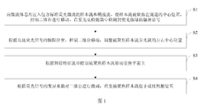
- FIG. 1 is a flow chart of a binary optical device-based microfluidic chip automatic alignment system according to an embodiment of the present invention
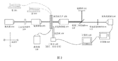
- FIG. 2 is a schematic structural view of a microfluidic chip automatic alignment system based on a binary optical device according to an embodiment of the present invention
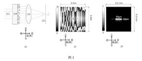
- FIG. 3 is a schematic diagram of a rectangular optical spot in which a binary optical device is laser shaped and homogenized to form a quasi-flat top according to an embodiment of the present invention
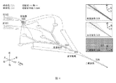
- FIG. 4 is a schematic view of an internal microfluidic channel of a microfluidic chip according to an embodiment of the present invention
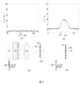
- FIG. 5 is a schematic diagram showing changes in a signal outputted by a photodetecting device and a change in position of a sample stream after focusing in step S1 of an embodiment of the present invention
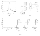
- FIG. 6 is a schematic diagram showing changes in signals outputted by the photodetecting device and positional changes of the sample stream after focusing in step S2 of an embodiment of the present invention
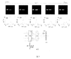
- FIG. 7 is a schematic diagram showing a signal change outputted by the photodetecting device and a position change of the sample stream after focusing, and an energy distribution of the spot when the focus is off, in step S3 of the embodiment of the present invention
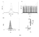
- Fig. 8 is a schematic view showing the optimum irradiation position obtained by right and left fine adjustment in step S4 of one embodiment of the present invention.
- FIG. 1 is a flow chart of a method for automatically aligning a microfluidic chip based on a binary optical device according to an embodiment of the present invention
- FIG. 2 is a structure of a microfluidic chip automatic alignment system based on a binary optical device according to an embodiment of the present invention; schematic diagram.
- a method for automatically aligning a microfluidic chip based on a binary optical device includes the following A laser 103, a binary optical device 104, a focusing objective lens 105, a microfluidic chip 106, a light collecting objective lens 107, a filter 113, a photodetector 114, a computer 116, a two-dimensional table 109, and fluorescent microspheres.
- the laser 103 is used to emit a laser that is shaped by the binary optics 104 and focused by the focusing objective 105 into a desired spot to form a designed spot on the focal plane of the focusing objective 105.
- the spot illumination illuminates the fluorescent microspheres in the microfluidic chip 106 to cause the fluorescent microspheres to fluoresce.
- the fluorescence is collected by the light collecting objective 107 and filtered by the filter 113 to enter the photodetector 114.
- Photodetector 114 converts the fluorescent signal into an electrical signal.
- the computer 116 discriminates the position of the microfluidic chip 106 based on the waveform characteristics of the electrical signals and controls the two-dimensional table 109 to adjust the position of the microfluidic chip 106.
- the detected sample stream and sheath flow enter the waste container 110, and the viewing screen 111 can be used to observe the spot.
- S1 injecting a sample stream and a sheath liquid stream containing a standard fluorescent microfluid into the microfluidic chip, so that the sample stream is focused at a center position of the flow channel, and the two-dimensional stage is controlled to move until the fluorescent microsphere is detected in the photodetector. Pulse signal.
- microfluidic chip 106 is mounted on the holder 108 of the two-dimensional table 109.
- sample stream 321 and sheath fluid stream 322 are injected into microfluidic chip 106 by pump 101 and pump 102, respectively, and sheath fluid stream 322 is shunted through splitter 323, causing sample stream 321 to pass through vertical focus 324 and The horizontal focus 325 is then focused at the center position 326 of the flow channel, ultimately forming a focused sample stream 327.
- the flow rates of the sample stream 321 and the sheath fluid stream 322 were 1 ⁇ l/s and 120 ⁇ l/s, respectively, and the flow channel section was 316 ⁇ m ⁇ 163 ⁇ m, and the sample flow rate was 4.8 m/s.
- Light ray 211 is shaped by binary optics 104 and focused by focusing lens 105 to form a focused spot 23 on the focal plane. Initially, the output of photodetector 114 is a noise signal, and the output waveform of oscilloscope 115 is as shown in FIG. Thereafter, the two-dimensional stage 109 is controlled to move left and right and back and forth until the pulse signal of the fluorescent microballoon 431 is detected in the photosensor 114.
- the focused sample stream 327 is before and after the focal plane 212, and the focused sample stream 327 is within the illumination range of the spot 23.
- an initial adjustment range can be determined so that the fluorescent pulse signal can be adjusted as quickly as possible.
- the two-dimensional table 109 is controlled to move until the focused sample stream 327 is located at the left and right center positions of the spot.
- step S2 further includes:
- the two-dimensional stage 109 is controlled to move to the left until the photodetector 114 detects the left extreme position of the fluorescent signal, and records the left extreme position.
- S202 Control the two-dimensional table to move to the right until the photodetector 114 does not detect the right extreme position of the fluorescent signal, and record the right extreme position;
- S203 Control the two-dimensional table to move until the focused sample stream is located at an intermediate position between the left limit position and the right limit position;
- the two-dimensional table moves to the left to move to the left perpendicular to the line between the focusing objective lens 105 and the light collecting objective lens 107, and the two-dimensional table moves to the right to be perpendicular to the line between the focusing objective lens 105 and the light collecting objective lens 107. move to the right.
- the laser is shaped by the binary optics 104 and focused by the focusing objective lens 105, a flat-topped rectangular spot 23 with a sharp boundary can be obtained on the focal plane 212, the long side of which is perpendicular to the liquid.
- the flow direction of the flow the short side is parallel to the direction of the liquid flow.
- the front and rear adjustment two-dimensional table 109 adjusts the position of the microfluidic chip 106 until the maximum pulse amplitude is obtained, at which time the focused sample stream 327 is located near the focal plane 212 of the focusing lens 105.
- the microfluidic chip 106 is adjusted to the left until there is no left extreme position of the fluorescent signal, at which time the focused sample stream 327 is located just to the left outer side of the spot; then the microfluidic chip 106 is adjusted to the right, at which point the fluorescent signal appears again, continuing to the right Adjust until there is no more fluorescent signal, at which point the focused sample stream 327 is located just to the right outside of the spot. Based on the two right extreme positions without the fluorescent signal, the microfluidic chip 106 is adjusted such that the focused sample stream 327 is intermediate the two positions, with the focused sample stream 327 being located on the left and right centerlines 56 of the spot. After the above adjustment, the focused sample stream 327 is located near the focal plane 212 and is located on the left and right centerlines of the spot.
- S3 Control the two-dimensional table movement according to the preset characteristic waveform until the focused sample stream 327 is located on the focal plane.
- step S3 further includes:
- S301 setting a preset waveform characteristic of a fluorescent pulse signal of the single fluorescent microsphere 431 when the focused sample stream 327 is located on and near the focal plane;
- S302 Control the two-dimensional table 109 to move forward and backward until the computer-acquired waveform feature coincides with the preset waveform feature on the focal plane to stop the two-dimensional motion adjustment.
- the focused sample stream 327 is located on the focal plane 212 of the focusing objective 105.
- the spot can only have the best uniformity and precise size on the focal plane 212.
- the spot will be deformed 601 to 605 according to the distance from the focal plane and the front and rear positions.
- the fluorescent signal emitted by them changes 606-610.
- the characteristics of the waveform it is possible to determine not only whether the focused sample stream 327 is located before the focal plane 212 or after the focal plane, but also the distance from the focal plane.
- the front and rear positions of the microfluidic chip 106 are adjusted, and the focused sample stream 327 has been accurately adjusted on the focal plane 212 when the waveform of the fluorescent signal conforms to the waveform characteristics of the sample stream on the focal plane.
- S4 The two-dimensional stage is fine-tuned according to the coefficient of variation of the fluorescence signal until the focused sample stream 327 is at the optimal illumination position.
- step S4 further includes:
- S401 Control the two-dimensional table to perform fine adjustment in the left and right direction, and collect a coefficient of variation of the fluorescent signal during the moving process;
- the position 741 of the focused sample stream 327 can be finely adjusted left and right.
- Fluorescent pulse The area 711 is the intensity of the fluorescent signal, and the fluorescent signal 72 of 10,000 fluorescent microspheres 431 is collected. A histogram 73 of these signal intensities is plotted and a gate 731 is used to remove the signal deviating from the mean and the coefficient of variation of the signal within the gate is calculated.
- the microfluidic chip 106 is finely adjusted to the left and right by the position 741 of the focused sample stream 327, and is the optimum illumination position when the coefficient of variation is the smallest. At this time, the focused sample stream 327 is not only accurately adjusted on the focal plane but also at the optimum illumination position, and the adjustment is completed.
- step S4 the method further includes:
- S5 Pass the cleaning agent to clean the flow path. In order to pass the sample stream containing the biological particles and the sheath fluid flow to the flow channel for detection after washing.
- Embodiments of the present invention also disclose a binary optical device-based microfluidic chip automatic alignment system including the following hardware: laser 103, binary optical device 104, focusing objective lens 105, microfluidic chip 106, light collecting objective lens 107
- the laser 103 is used to emit a laser that is shaped by the binary optics 104 and focused by the focusing objective 105 into a desired spot 23.
- the spot illumination illuminates the fluorescent microspheres in the microfluidic chip 106 to cause the fluorescent microspheres to fluoresce.
- the fluorescence is collected by the light collecting objective 107 and filtered by the filter 113 to enter the photodetector 114.
- Photodetector 114 converts the fluorescent signal into an electrical signal.
- Pumps 101 and 102 or other liquid flow source inject a sample stream and a sheath flow containing standard fluorescent microfluids into the microfluidic core 106, such that after the sample stream is focused at the center of the flow channel, computer 116 controls the two-dimensional table Moving to a pulse signal of the fluorescent microsphere detected in the photodetector; the computer 116 is further configured to control the two-dimensional movement to position the focused sample stream 327 at a central position of the spot according to the extreme position of the fluorescent signal; the computer 116 is also used to Controlling the two-dimensional table movement according to the preset characteristic waveform causes the focused sample stream 327 to be located on the focal plane; the computer 116 is further configured to fine tune the two-dimensional table according to the coefficient of variation of the fluorescence signal until the focused sample stream 327 is
- the computer 116 is further configured to: control the two-dimensional table 109 to move to the left until the photodetector 114 does not detect the left extreme position of the fluorescent signal, and record the left extreme position; control the two-dimensional table 109 Moving to the right until the photodetector 114 detects the right extreme position of the fluorescent signal and recording the right extreme position; controlling the two-dimensional table 109 to move so that the focused sample stream 327 is in the middle of the left extreme position and the right extreme position; The two-dimensional table 109 is moved to the left to move to the left perpendicular to the line between the focusing objective lens 105 and the light collecting objective lens 107, and the two-dimensional table 109 is moved to the right to be perpendicular to the focusing objective lens and the light. The line connecting the objective lenses moves to the right.
- the computer 116 is further configured to: set a preset waveform feature when the fluorescent microsphere 431 is located on the focal plane and in the vicinity of the focused sample stream 327; and control the two-dimensional table 109 to move forward and backward.
- the two-dimensional stage 109 movement adjustment focused sample stream 327 is located on the focal plane 212 of the first focusing objective 105 until the waveform feature acquired by the computer 116 coincides with the preset waveform characteristic on the focal plane.
- the computer 116 is further configured to: control the two-dimensional table 109 to advance in the left-right direction The line moves to adjust the position of the focused sample stream 327 in the left-right direction, and collects the coefficient of variation of the fluorescent signal during the movement; the two-dimensional stage 109 is controlled to move to the position corresponding to the smallest coefficient of variation.
- photodetector 114 is a photo-electric tube, a photomultiplier tube array, a charge-carrying unit, or a photodiode.
- Embodiments of the present invention also disclose an apparatus comprising: one or more processors; a memory; one or more programs, the one or more programs being stored in the memory when the one or more When the processors are executed, the binary optical device-based microfluidic chip automatic alignment method as described in the above embodiments is performed.
- Embodiments of the present invention also disclose a non-volatile computer storage medium storing one or more programs that, when executed by a device, cause the device to perform the operations described in the above embodiments.
Landscapes
- Chemical & Material Sciences (AREA)
- Dispersion Chemistry (AREA)
- Physics & Mathematics (AREA)
- Health & Medical Sciences (AREA)
- Life Sciences & Earth Sciences (AREA)
- Analytical Chemistry (AREA)
- Biochemistry (AREA)
- General Health & Medical Sciences (AREA)
- General Physics & Mathematics (AREA)
- Immunology (AREA)
- Pathology (AREA)
- Investigating, Analyzing Materials By Fluorescence Or Luminescence (AREA)
Abstract
一种基于二元光学器件(104)的微流体芯片(106)自动对准方法和系统,该方法包括:向微流体芯片(106)注入包含标准荧光微流的样本流(321)和鞘液流(322),使样本流(321)被聚焦在流道的中心位置,控制二维台(109)进行移动,直至光电检测器(114)中检测到荧光微球的脉冲信号;根据出现荧光信号的极限位置,调整被聚焦样本流(327)位于光斑(23)的中心位置;根据预设特征波形控制二维台(109)移动,调整被聚焦样本流(327)位于焦平面(212)上;根据荧光信号的变异系数对二维台(109)进行微调直至最佳照射位置。本申请具有如下优点:采用二元光学器件(104)作为光斑整形器件,并根据荧光微粒受激光照射后发出的荧光信号的特征判别微流体芯片(106)的位置,并据此调节被聚焦样本流(327)至最佳位置,从而实现最佳的检测效果和一致性。
Description
相关申请的交叉引用
本申请要求清华大学于2016年8月22日递交的、发明名称为“基于二元光学器件的微流体芯片自动对准方法和系统”的,中国专利申请号为“201610704513.X”的优先权。
发明涉及流式细胞术、物理光学和微流体领域,具体涉及一种基于二元光学器件的微流体芯片自动对准方法和系统。
得益于微流体技术的发展以及流式细胞术在细胞检测方面的强大功能,近年来涌现出了大量基于微流体芯片的片上流式细胞仪。这些微流体芯片能够将细胞等生物微粒聚焦在流道的中心位置,而后这些生物微粒将被激光照射并发射出散射光和荧光。发射出的光信号被后续的光电检测传感器收集,并传入分析系统进行分析。一般用于照射的激光光斑尺寸仅为数十微米,这就要求被聚焦后的生物微粒恰好处于激光光斑照射的范围内且在焦平面上。对于传统的流式细胞仪而言,这一对准过程可以手动调节,因为调节后可将各个部件固定、后续除矫正外不需要频繁调节。但对于微流体芯片而言,由于需要频繁更换微流体芯片,以消除交叉污染,而手动调节费时费力且难以保证一致性。
发明内容
本发明实施例提供一种适合于批量化生产的多层微流体芯片制作方法、系统、设备及计算机存储介质,旨在适合批量生产且降低成本。
本发明实施例是这样实现的,一种基于二元光学器件的微流体芯片自动对准方法,包括激光器、二元光学器件、聚焦物镜、微流体芯片、光收集物镜、滤光片、光电检测器、计算机、二维台和荧光微球,所述激光器用于发射激光,所述激光经过所述二元光学器件整形并被聚焦物镜聚焦为所需光斑,所述光斑照射位于所述微流体芯片中所述荧光微球以使所述荧光微球发出荧光,所述荧光经所述光收集物镜收集并被所述滤光片滤除杂光后进入所述光电检测器,所述光电检测器将荧光信号转换为电信号,所述计算机根据所述电信
号的波形特征判别被聚焦样本流的位置,并控制所述二维台调节所述微流体芯片中的所述被聚焦样本流的位置;所述方法包括以下步骤:S1:向所述微流体芯片注入包含标准荧光微流的样本流和鞘液流,使所述样本流被聚焦在流道的中心位置,控制所述二维台进行移动,直至所述光电检测器中检测到所述荧光微球的脉冲信号;S2:根据出现所述荧光信号的极限位置,控制所述二维台移动,调整被所述聚焦样本流至所述光斑的左右中心位置;S3:根据预设特征波形控制所述被聚焦样本流移动至焦平面上;S4:根据所述荧光信号的变异系数对所述二维台进行微调,直至所述被聚焦样本流位于最佳照射位置。
本发明实施例的另一目的在于提供一种基于二元光学器件的微流体芯片自动对准系统,包括激光器、二元光学器件、聚焦物镜、微流体芯片、光收集物镜、滤光片、光电检测器、计算机、二维台和荧光微球,所述激光器用于发射激光,所述激光经过所述二元光学器件整形并被聚焦物镜聚焦为所需光斑,所述光斑照射位于所述微流体芯片中所述荧光微球以使所述荧光微球发出荧光,所述荧光经所述光收集物镜收集并被所述滤光片滤除杂光后进入所述光电检测器,所述光电检测器将荧光信号转换为电信号;泵或其他液流源在向所述微流体芯片注入包含标准荧光微流的样本流和鞘液流,使所述样本流被聚焦在流道的中心位置后,所述计算机控制所述二维台进行移动所述光电检测器中检测到所述荧光微球的脉冲信号;所述计算机还用于根据出现所述荧光信号的极限位置,控制所述二维台移动、直至所述微流体芯片中被聚焦样本流位于所述光斑的中心位置;所述计算机还用于根据预设的特征波形控制所述二维台移动,直至所述被聚焦样本流位于所述聚焦物镜的焦平面上;所述计算机还用于根据所述荧光信号的变异系数对所述聚焦样本流进行微调直至最佳照射位置。
本发明实施例的另一目的在于提供一种设备,包括:一个或者多个处理器;存储器;一个或者多个程序,所述一个或者多个程序存储在所述存储器中,当被所述一个或者多个处理器执行时,执行上述实施例所述的基于二元光学器件的微流体芯片自动对准方法。
本发明实施例的另一目的在于提供一种非易失性计算机存储介质,所述计算机存储介质存储有一个或者多个程序,当所述一个或者多个程序被一个设备执行时,使得所述设备执行本发明上述实施例的基于二元光学器件的微流体芯片自动对准方法。
本发明实施例的采用二元光学器件作为光斑整形器件,并根据标准荧光微粒受激光照射后发出的荧光信号的特征判别微流体芯片中被聚焦样本流的位置,并据此调节微流体芯片使被聚焦样本流位于最佳位置,从而实现最佳的检测效果。
为了更清楚地说明本发明实施例中的技术方案,下面将对实施例或现有技术描述中所需要使用的附图作简单地介绍,显而易见地,下面描述中的附图仅仅是本发明的一些实施例,对于本领域普通技术人员来讲,在不付出创造性劳动性的前提下,还可以根据这些附图获得其他的附图。
图1是本发明实施例的基于二元光学器件的微流体芯片自动对准系统的流程图;
图2是本发明一个实施例的基于二元光学器件的微流体芯片自动对准系统的结构示意图;
图3是本发明一个实施例的二元光学器件对激光整形并匀化形成准平顶的矩形光斑示意图;
图4是本发明一个实施例的微流体芯片的内部微流道示意图;
图5是本发明一个实施例的步骤S1中光电检测器件输出的信号变化,以及聚焦后样本流的位置变化示意图;
图6是本发明一个实施例的步骤S2中光电检测器件输出的信号变化,以及聚焦后样本流的位置变化示意图;
图7是本发明一个实施例的步骤S3中光电检测器件输出的信号变化,以及聚焦后样本流的位置变化,离焦时光斑的能量分布情况示意图;
图8是本发明一个实施例的步骤S4中左右微调获得最佳照射位置时的示意图。
下面详细描述本发明的实施例,所述实施例的示例在附图中示出,其中自始至终相同或类似的标号表示相同或类似的元件或具有相同或类似功能的元件。下面通过参考附图描述的实施例是示例性的,仅用于解释本发明,而不能理解为对本发明的限制。
参照下面的描述和附图,将清楚本发明的实施例的这些和其他方面。在这些描述和附图中,具体公开了本发明的实施例中的一些特定实施方式,来表示实施本发明的实施例的原理的一些方式,但是应当理解,本发明的实施例的范围不受此限制。相反,本发明的实施例包括落入所附加权利要求书的精神和内涵范围内的所有变化、修改和等同物。
以下结合附图描述根据本发明实施例的基于二元光学器件的微流体芯片自动对准方法和系统。
图1是本发明一个实施例的基于二元光学器件的微流体芯片自动对准方法的流程图,图2是本发明一个实施例的基于二元光学器件的微流体芯片自动对准系统的结构示意图。
如图1和图2所示,一种基于二元光学器件的微流体芯片自动对准方法,包括如下硬
件:激光器103、二元光学器件104、聚焦物镜105、微流体芯片106、光收集物镜107、滤光片113、光电检测器114、计算机116、二维台109和荧光微球。激光器103用于发射激光,激光经过二元光学器件104整形并被聚焦物镜105聚焦为所需光斑,在聚焦物镜105的焦平面上形成所设计的光斑。光斑照射位于微流体芯片106中荧光微球以使荧光微球发出荧光。荧光经光收集物镜107收集并被滤光片113滤除杂光后进入光电检测器114。光电检测器114将荧光信号转换为电信号。计算机116根据电信号的波形特征判别微流体芯片106的位置,并控制二维台109调节微流体芯片106的位置。经过检测的样本流和鞘液流进入废液桶110中,观察屏111可用于观察光斑。
本发明实施例的基于二元光学器件的微流体芯片自动对准方法包括以下步骤:
S1:向微流体芯片注入包含标准荧光微流的样本流和鞘液流,使样本流被聚焦在流道的中心位置,控制二维台进行移动,直至光电检测器中检测到荧光微球的脉冲信号。
具体地,将微流体芯片106安装在二维台109的固定架108上。如图3和图4所示,通过泵101和泵102分别向微流体芯片106注入样本流321和鞘液流322,鞘液流322经过分流器323分流,使样本流321经过垂直聚焦324和水平聚焦325后被聚焦在流道的中心位置326,最终形成被聚焦样本流327。样本流321和鞘液流322的流量分别为1μl/s和120μl/s,流道截面为316μm×163μm,样本流流速为4.8m/s。光线211经过二元光学器件104整形并被聚焦透镜105聚焦,在焦平面上形成聚焦光斑23。起始时,光电检测器114的输出为噪声信号,示波器115的输出波形如图5所示。之后,控制二维台109左右和前后移动,直至光电传感器114中检测到荧光微球431的脉冲信号。此时,被聚焦样本流327在焦平面212前后,聚焦后样本流327在光斑23的照射范围内。一般,根据使用经验,可确定一个初始的调节范围,从而能够尽快调节出荧光脉冲信号。
S2:根据出现荧光信号的极限位置,控制二维台109移动直至被聚焦样本流327位于光斑的左右中心位置。
在本发明的一个实施例中,步骤S2进一步包括:
S201:控制二维台109向左移动,直至光电探测器114检测不到荧光信号的左极限位置,并记录左极限位置。
S202:控制二维台向右移动,直至光电探测器114检测不到荧光信号的右极限位置,并记录右极限位置;
S203:控制二维台移动直至被聚焦样本流位于左极限位置和右极限位置的中间位置;
其中,二维台向左移动为垂直于所述聚焦物镜105和光收集物镜107之间的连线向左移动,二维台向右移动为垂直于聚焦物镜105和光收集物镜107之间的连线向右移动。
具体地,如图6所示,由于激光采用二元光学器件104整形并被聚焦物镜透镜105聚焦,因而在焦面上212可以获得一个边界清晰的平顶矩形光斑23,其长边垂直于液流的流动方向,短边与液流方向平行。前后调节二维台109调节微流体芯片106的位置,直至获得最大脉冲幅值,此时被聚焦样本流327位于聚焦透镜105的焦平面212附近。向左调节微流体芯片106直至没有荧光信号的左极限位置,此时被聚焦样本流327恰好位于光斑的左外侧;再向右调节微流体芯片106,此时荧光信号又显现出来,持续向右调节直至再次没有荧光信号,此时被聚焦样本流327恰好位于光斑的右外侧。根据两个没有荧光信号的右极限位置,调节微流体芯片106使被聚焦样本流327位于这两个位置的中间位置,此时被聚焦样本流327位于光斑的左右中线上56。经过上述调节,被聚焦样本流327位于焦平面212附近,且位于光斑的左右中线上。
S3:根据预设特征波形控制二维台移动直至被聚焦样本流327位于焦平面上。
在本发明的一个实施例中,步骤S3进一步包括:
S301:设定被聚焦样本流327位于焦面上以及附近时单个荧光微球431的荧光脉冲信号的预设波形特征;
S302:控制二维台109向前后方向移动,直至在计算机采集波形特征与焦面上预设波形特征相符合时停止二维台移动调整被聚焦样本流327位于聚焦物镜105的焦面212上。
具体地,如图7所示,由于激光采用二元光学器件104整形,光斑只有在焦平面212上才能有最佳的均匀性和精准的尺寸。离焦时,根据距离焦面的距离和前后位置,光斑会发生变形601~605。因而,当标准荧光微球431粒经过光斑时,其发射出的荧光信号会发生变化606~610。根据波形的特征不仅能够判别被聚焦样本流327位于焦面212前还是焦面后,还能判别其距离焦面的距离。调节微流体芯片106的前后位置,当荧光信号的波形符合样本流位于焦面上时的波形特征时,被聚焦样本流327已经被精确地调节在焦平212上。
S4:根据荧光信号的变异系数对二维台进行微调直至被聚焦样本流327位于最佳照射位置。
在本发明的一个实施例中,步骤S4进一步包括:
S401:控制二维台在左右方向上进行微调,并采集在移动过程中荧光信号的变异系数;
S402:控制二维台移动至变异系数最小对应的位置。
具体地,如图8所示,虽然被聚焦样本流327已经被精确地调节在焦平面212上,但由于激光采用二元光学器件整形,故光斑不是绝对的平顶(不是绝对均匀)。这将影响照射质量和测试结果。因而,可以左右细微调节被聚焦样本流327的位置741。取荧光脉冲的
面积711为荧光信号的强度,收集计算10000个荧光微球431的荧光信号72。绘制这些信号强度的直方图73并用一个门731去除偏离均值的信号,计算门内信号的变异系数。左右细微调节微流体芯片106既被聚焦样本流327的位置741,当变异系数最小时即为最佳的照射位置。此时,被聚焦样本流327不仅被精确地调节在焦平面上,还处于最佳的照射位置,至此完成调节。
在本发明的一个实施例中,在步骤S4之后还包括:
S5:通入清洗剂清洗流道。以便在清洗之后可向流道再次通入包含生物微粒的样本流和鞘液流进行检测。
本发明的实施例还公开了一种基于二元光学器件的微流体芯片自动对准系统,包括如下硬件:激光器103、二元光学器件104、聚焦物镜105、微流体芯片106、光收集物镜107、滤光片113、光电检测器114、计算机116、二维台109和荧光微球431。激光器103用于发射激光,激光经过二元光学器件104整形并被聚焦物镜105聚焦为所需光斑23。光斑照射位于微流体芯片106中荧光微球以使荧光微球发出荧光。荧光经光收集物镜107收集并被滤光片113滤除杂光后进入光电检测器114。光电检测器114将荧光信号转换为电信号。泵101和102或其他液流源在向微流体芯106片注入包含标准荧光微流的样本流和鞘液流,使样本流被聚焦在流道的中心位置后,计算机116控制二维台进行移动至光电检测器中检测到荧光微球的脉冲信号;计算机116还用于根据出现荧光信号的极限位置,控制二维台移动使被聚焦样本流327位于光斑的中心位置;计算机116还用于根据预设的特征波形控制二维台移动使被聚焦样本流327位于焦平面上;计算机116还用于根据荧光信号的变异系数对二维台进行微调直至被聚焦样本流327位于最佳照射位置。
在本发明的一个实施例中,计算机116进一步用于:控制二维台109向左移动,直至光电检测器114检测不到荧光信号的左极限位置,并记录左极限位置;控制二维台109向右移动,直至光电检测器114检测不到荧光信号的右极限位置,并记录右极限位置;控制二维台109移动使被聚焦样本流327位于左极限位置和右极限位置的中间位置;其中,二维台109向左移动为垂直于所述聚焦物镜105和所述光收集物镜107之间的连线向左移动,二维台109向右移动为垂直于所述聚焦物镜和所述光收集物镜之间的连线向右移动。
在本发明的一个实施例中,计算机116进一步用于:设定被聚焦样本流327中荧光微球431位于焦面上以及附近时的预设波形特征;控制二维台109向前后方向移动,直至在计算机116采集波形特征与焦面上预设波形特征相符合时停止二维台109移动调整被聚焦样本流327位于第一聚焦物镜105的焦面212上。
在本发明的一个实施例中,计算机116进一步用于:控制二维台109在左右方向上进
行移动以调节被聚焦样本流327在左右方向的位置,并采集在移动过程中荧光信号的变异系数;控制二维台109移动至变异系数最小对应的位置。
在本发明的一个实施例中,光电检测器114为光电培增管、光电倍增管阵列、电荷藕荷单元或光电二极管。
需要说明的是,本发明实施例的基于二元光学器件的微流体芯片自动对准系统的具体实施方式与本发明实施例的基于二元光学器件的微流体芯片自动对准方法的具体实施方式相同,不再赘述。
本发明的实施例还公开了一种设备,包括:一个或者多个处理器;存储器;一个或者多个程序,所述一个或者多个程序存储在所述存储器中,当被所述一个或者多个处理器执行时,执行如上述实施例所述的基于二元光学器件的微流体芯片自动对准方法。
本发明的实施例还公开了一种非易失性计算机存储介质,计算机存储介质存储有一个或者多个程序,当一个或者多个程序被一个设备执行时,使得设备执行上述实施例所述的基于二元光学器件的微流体芯片自动对准方法。
另外,本发明实施例的批量化生产的多层微流体芯片制作方法、系统和非易失性计算机存储介质的其它构成以及作用对于本领域的技术人员而言都是已知的,为了减少冗余,不做赘述。
在本说明书的描述中,参考术语“一个实施例”、“一些实施例”、“示例”、“具体示例”、或“一些示例”等的描述意指结合该实施例或示例描述的具体特征、结构、材料或者特点包含于本发明的至少一个实施例或示例中。在本说明书中,对上述术语的示意性表述不一定指的是相同的实施例或示例。而且,描述的具体特征、结构、材料或者特点可以在任何的一个或多个实施例或示例中以合适的方式结合。
尽管已经示出和描述了本发明的实施例,本领域的普通技术人员可以理解:在不脱离本发明的原理和宗旨的情况下可以对这些实施例进行多种变化、修改、替换和变型,本发明的范围由权利要求及其等同限定。
Claims (12)
- 一种基于二元光学器件的微流体芯片自动对准方法,其特征在于,包括激光器、二元光学器件、聚焦物镜、微流体芯片、光收集物镜、滤光片、光电检测器、计算机、二维台和荧光微球,所述激光器用于发射激光,所述激光经过所述二元光学器件整形并被聚焦物镜聚焦为所需光斑,所述光斑照射位于所述微流体芯片中所述荧光微球以使所述荧光微球发出荧光,所述荧光经所述光收集物镜收集并被所述滤光片滤除杂光后进入所述光电检测器,所述光电检测器将荧光信号转换为电信号,所述计算机根据所述电信号的波形特征判别被聚焦样本流的位置,并控制所述二维台调节所述微流体芯片中的所述被聚焦样本流的位置;所述方法包括以下步骤:S1:向所述微流体芯片注入包含标准荧光微流的样本流和鞘液流,使所述样本流被聚焦在流道的中心位置,控制所述二维台进行移动,直至所述光电检测器中检测到所述荧光微球的脉冲信号;S2:根据出现所述荧光信号的极限位置,控制所述二维台移动,调整被所述聚焦样本流至所述光斑的左右中心位置;S3:根据预设特征波形控制所述被聚焦样本流移动至焦平面上;S4:根据所述荧光信号的变异系数对所述二维台进行微调,直至所述被聚焦样本流位于最佳照射位置。
- 根据权利要求1所述的基于二元光学器件的微流体芯片自动对准方法,其特征在于,步骤S2进一步包括:S201:控制所述二维台向左移动,直至所述光电探测器探测不到荧光信号的左极限位置,并记录所述左极限位置;S202:控制所述二维台向右移动,直至所述光电探测器探测不到荧光信号的右极限位置,并记录所述右极限位置;S203:控制所述二维台移动至所述被聚焦样本流位于所述左极限位置和所述右极限位置的中间位置;其中,所述二维台向左移动为垂直于所述第一聚焦物镜和所述第二聚焦物镜之间的连线向左移动,所述二维台向右移动为垂直于所述第一聚焦物镜和所述第二聚焦物镜之间的连线向右移动。
- 根据权利要求2所述的基于二元光学器件的微流体芯片自动对准方法,其特征在于,步骤S3进一步包括:S301:设定所述被聚焦样本流位于所述焦面上以及附近时的荧光微球发出的荧光脉冲信号的预设波形特征;S302:控制所述二维台向前后方向移动,直至在所述计算机采集波形特征与所述预设波形特征相符合时停止所述二维台移动调整所述被聚焦样本流至所述第一聚焦物镜的焦面上。
- 根据权利要求3所述的基于二元光学器件的微流体芯片自动对准方法,其特征在于,步骤S4进一步包括:S401:控制所述二维台在左右方向上进行调节,并采集在调节过程中荧光信号的变异系数;S402:控制所述二维台移动使所述被聚焦样本流位于所述变异系数最小对应的位置。
- 根据权利要求1-4任一项所述的基于二元光学器件的微流体芯片自动对准方法,其特征在于,在步骤S4之后还包括:S5:通入清洗剂清洗流道。
- 一种基于二元光学器件的微流体芯片自动对准系统,其特征在于,包括激光器、二元光学器件、聚焦物镜、微流体芯片、光收集物镜、滤光片、光电检测器、计算机、二维台和荧光微球,所述激光器用于发射激光,所述激光经过所述二元光学器件整形并被聚焦物镜聚焦为所需光斑,所述光斑照射位于所述微流体芯片中所述荧光微球以使所述荧光微球发出荧光,所述荧光经所述光收集物镜收集并被所述滤光片滤除杂光后进入所述光电检测器,所述光电检测器将荧光信号转换为电信号;泵或其他液流源在向所述微流体芯片注入包含标准荧光微流的样本流和鞘液流,使所述样本流被聚焦在流道的中心位置后,所述计算机控制所述二维台进行移动所述光电检测器中检测到所述荧光微球的脉冲信号;所述计算机还用于根据出现所述荧光信号的极限位置,控制所述二维台移动、直至所述微流体芯片中被聚焦样本流位于所述光斑的中心位置;所述计算机还用于根据预设的特征波形控制所述二维台移动,直至所述被聚焦样本流位于所述聚焦物镜的焦平面上;所述计算机还用于根据所述荧光信号的变异系数对所述聚焦样本流进行微调直至最佳照射位置。
- 根据权利要求6所述的基于二元光学器件的微流体芯片自动对准系统,其特征在于,所述计算机进一步用于:控制所述二维台向左移动,直至所述光电探测器探测不到荧光信号的左极限位置,并记录所述左极限位置;控制所述二维台向右移动,直至所述光电探测器探测不到荧光信号的右极限位置,并记录所述右极限位置;控制所述二维台移动、直至所述被聚焦样本流位于所述左极限位置和所述右极限位置的中间位置;其中,所述二维台向左移动为垂直于所 述聚焦物镜和所述光收集聚焦物镜之间的连线向左移动,所述二维台向右移动为垂直于所述第一聚焦物镜和所述第二聚焦物镜之间的连线向右移动。
- 根据权利要求7所述的基于二元光学器件的微流体芯片自动对准系统,其特征在于,所述计算机进一步用于:设定所述样本流位于所述焦面上以及附近时荧光微球发出的荧光脉冲信号的的预设波形特征;控制所述二维台向前后方向移动,直至在所述计算机采集波形特征与所述预设焦面上波形特征相符合时停止所述二维台移动调整直至所述被聚焦样本流位于所述第一聚焦物镜的焦面上。
- 根据权利要求8所述的基于二元光学器件的微流体芯片自动对准系统,其特征在于,所述计算机进一步用于:控制所述二维台在左右方向上进行移动,并采集在移动过程中荧光信号的变异系数;控制所述二维台移动直至所述被聚焦样本流位于所述变异系数最小对应的位置。
- 根据权利要求6-9任一项所述的基于二元光学器件的微流体芯片自动对准系统,其特征在于,所述光电检测器为光电培增管、光电倍增管阵列、电荷藕荷单元或光电二极管。
- 一种设备,其特征在于,包括:一个或者多个处理器;存储器;一个或者多个程序,所述一个或者多个程序存储在所述存储器中,当被所述一个或者多个处理器执行时,执行如权利要求1-5任一项所述的适合于批量化生产的多层微流体芯片制作方法。
- 一种非易失性计算机存储介质,其特征在于,所述计算机存储介质存储有一个或者多个程序,当所述一个或者多个程序被一个设备执行时,使得所述设备执行如权利要求1-5任一项所述的适合于批量化生产的多层微流体芯片制作方法。
Applications Claiming Priority (2)
| Application Number | Priority Date | Filing Date | Title |
|---|---|---|---|
| CN201610704513.X | 2016-08-22 | ||
| CN201610704513.XA CN106383081B (zh) | 2016-08-22 | 2016-08-22 | 基于二元光学器件的微流体芯片自动对准方法和系统 |
Publications (1)
| Publication Number | Publication Date |
|---|---|
| WO2018035977A1 true WO2018035977A1 (zh) | 2018-03-01 |
Family
ID=57916889
Family Applications (1)
| Application Number | Title | Priority Date | Filing Date |
|---|---|---|---|
| PCT/CN2016/104946 Ceased WO2018035977A1 (zh) | 2016-08-22 | 2016-11-07 | 基于二元光学器件的微流体芯片自动对准方法和系统 |
Country Status (2)
| Country | Link |
|---|---|
| CN (1) | CN106383081B (zh) |
| WO (1) | WO2018035977A1 (zh) |
Cited By (2)
| Publication number | Priority date | Publication date | Assignee | Title |
|---|---|---|---|---|
| CN110487725A (zh) * | 2019-09-04 | 2019-11-22 | 新羿制造科技(北京)有限公司 | 能够自动聚焦的检测装置及相应的自动聚焦方法 |
| CN116196992A (zh) * | 2023-04-19 | 2023-06-02 | 苏州索真生物技术有限公司 | 一种微流控芯片及降低微流控芯片相邻通道互扰的方法 |
Families Citing this family (4)
| Publication number | Priority date | Publication date | Assignee | Title |
|---|---|---|---|---|
| WO2019200518A1 (zh) * | 2018-04-16 | 2019-10-24 | 清华大学 | 用于流式检测的多激光光束整形系统及方法 |
| CN108519332B (zh) * | 2018-04-28 | 2019-12-03 | 南通市肺科医院(南通市第六人民医院) | 全自动微孔板系统及用于该系统的计算机可读介质 |
| CN113008851B (zh) * | 2021-02-20 | 2024-04-12 | 大连海事大学 | 一种基于斜入式激发提高共聚焦结构微弱信号检测信噪比的装置 |
| CN113567397B (zh) * | 2021-08-11 | 2024-06-04 | 苏州索真生物技术有限公司 | 微流控芯片、微流控芯片通道定位结构及定位方法 |
Citations (4)
| Publication number | Priority date | Publication date | Assignee | Title |
|---|---|---|---|---|
| CN1954199A (zh) * | 2003-10-17 | 2007-04-25 | 英特尔公司 | 使用表面增强相干反斯托克斯拉曼光谱学检测少量分子的方法和设备 |
| CN202177564U (zh) * | 2011-07-08 | 2012-03-28 | 无锡荣兴科技有限公司 | 一种采用蓝色半导体激光器的血液细胞分析仪 |
| CN102998242A (zh) * | 2012-11-25 | 2013-03-27 | 中北大学 | 微流体细胞仪及制作方法 |
| US9341515B2 (en) * | 2011-02-11 | 2016-05-17 | University Of Central Florida Research Foundation, Inc. | Optical absorbance measurement apparatus, method, and applications |
Family Cites Families (3)
| Publication number | Priority date | Publication date | Assignee | Title |
|---|---|---|---|---|
| US4989977A (en) * | 1985-07-29 | 1991-02-05 | Becton, Dickinson And Company | Flow cytometry apparatus with improved light beam adjustment |
| JP4805416B1 (ja) * | 2010-03-31 | 2011-11-02 | 古河電気工業株式会社 | 光情報解析装置及び光情報解析方法 |
| CN103383338B (zh) * | 2013-07-23 | 2015-06-10 | 清华大学深圳研究生院 | 流式细胞测量仪和测量方法 |
-
2016
- 2016-08-22 CN CN201610704513.XA patent/CN106383081B/zh active Active
- 2016-11-07 WO PCT/CN2016/104946 patent/WO2018035977A1/zh not_active Ceased
Patent Citations (4)
| Publication number | Priority date | Publication date | Assignee | Title |
|---|---|---|---|---|
| CN1954199A (zh) * | 2003-10-17 | 2007-04-25 | 英特尔公司 | 使用表面增强相干反斯托克斯拉曼光谱学检测少量分子的方法和设备 |
| US9341515B2 (en) * | 2011-02-11 | 2016-05-17 | University Of Central Florida Research Foundation, Inc. | Optical absorbance measurement apparatus, method, and applications |
| CN202177564U (zh) * | 2011-07-08 | 2012-03-28 | 无锡荣兴科技有限公司 | 一种采用蓝色半导体激光器的血液细胞分析仪 |
| CN102998242A (zh) * | 2012-11-25 | 2013-03-27 | 中北大学 | 微流体细胞仪及制作方法 |
Cited By (3)
| Publication number | Priority date | Publication date | Assignee | Title |
|---|---|---|---|---|
| CN110487725A (zh) * | 2019-09-04 | 2019-11-22 | 新羿制造科技(北京)有限公司 | 能够自动聚焦的检测装置及相应的自动聚焦方法 |
| CN110487725B (zh) * | 2019-09-04 | 2024-05-28 | 新羿制造科技(北京)有限公司 | 能够自动聚焦的检测装置及相应的自动聚焦方法 |
| CN116196992A (zh) * | 2023-04-19 | 2023-06-02 | 苏州索真生物技术有限公司 | 一种微流控芯片及降低微流控芯片相邻通道互扰的方法 |
Also Published As
| Publication number | Publication date |
|---|---|
| CN106383081B (zh) | 2019-05-31 |
| CN106383081A (zh) | 2017-02-08 |
Similar Documents
| Publication | Publication Date | Title |
|---|---|---|
| WO2018035977A1 (zh) | 基于二元光学器件的微流体芯片自动对准方法和系统 | |
| TWI902555B (zh) | 用於追蹤具有可配置焦點偏移之樣本表面的自動對焦系統 | |
| KR102162213B1 (ko) | 이미지 형성 세포 계수기 | |
| EP3264153B1 (en) | Light sheet microscope and control method for light sheet microscope | |
| JP6275704B2 (ja) | 顕微鏡検査撮像システムにおいて対物レンズの焦点位置を決定するためのシステム、方法、およびデバイス | |
| US8941081B2 (en) | Microparticle measurement apparatus and microparticle analysis method | |
| CN108037310B (zh) | 一种用于显微粒子成像测速系统的图像采集装置及采集方法 | |
| CN105067568A (zh) | 自动聚焦式激光诱导击穿光谱检测系统及其检测方法 | |
| EP3268720A1 (en) | Methods, systems and apparatus for sorting and processing analytes | |
| CN103837515A (zh) | 一种共聚焦自动调节装置 | |
| CN109276229B (zh) | 一种用于光声显微成像的快速对焦系统及方法 | |
| JP2013513789A (ja) | 流れる液体中の発光粒子または光散乱粒子を検出する手段 | |
| CN114858764B (zh) | 一种可自动聚焦的荧光检测系统和自动聚焦方法 | |
| CN101796391A (zh) | 血液检查装置 | |
| CN115026449B (zh) | 一种紧聚焦飞秒激光光束的准直性调校方法及装置 | |
| CN115452784A (zh) | 自动对焦系统、基因测序系统及自动对焦方法 | |
| WO2014080932A1 (ja) | 光学顕微鏡、および、光学顕微鏡のオートフォーカス装置 | |
| JP2020137429A (ja) | 細胞観察システムおよび細胞観察方法 | |
| JP2018017970A (ja) | 光シート顕微鏡、及び、光シート顕微鏡の制御方法 | |
| CN114486910B (zh) | 一种平面光学元件表面疵病检测装置和检测方法 | |
| KR101653176B1 (ko) | 자동초점거리 조절 기능을 갖는 렌즈 검사장치 | |
| CN110196245A (zh) | 一种激光诱导击穿光谱检测系统 | |
| CN108010062B (zh) | 三维单分子追踪方法及装置 | |
| CN104266956A (zh) | 高内涵图像流式生物显微分析方法 | |
| CN109433282B (zh) | 一种台阶式生物芯片以及用于检测该生物芯片的基因测序装置 |
Legal Events
| Date | Code | Title | Description |
|---|---|---|---|
| 121 | Ep: the epo has been informed by wipo that ep was designated in this application |
Ref document number: 16913997 Country of ref document: EP Kind code of ref document: A1 |
|
| NENP | Non-entry into the national phase |
Ref country code: DE |
|
| 122 | Ep: pct application non-entry in european phase |
Ref document number: 16913997 Country of ref document: EP Kind code of ref document: A1 |