WO2018020846A1 - 撮像装置 - Google Patents
撮像装置 Download PDFInfo
- Publication number
- WO2018020846A1 WO2018020846A1 PCT/JP2017/021011 JP2017021011W WO2018020846A1 WO 2018020846 A1 WO2018020846 A1 WO 2018020846A1 JP 2017021011 W JP2017021011 W JP 2017021011W WO 2018020846 A1 WO2018020846 A1 WO 2018020846A1
- Authority
- WO
- WIPO (PCT)
- Prior art keywords
- light
- imaging device
- receiving element
- wavelength
- opening
- Prior art date
- Legal status (The legal status is an assumption and is not a legal conclusion. Google has not performed a legal analysis and makes no representation as to the accuracy of the status listed.)
- Ceased
Links
Images





Classifications
-
- H—ELECTRICITY
- H04—ELECTRIC COMMUNICATION TECHNIQUE
- H04N—PICTORIAL COMMUNICATION, e.g. TELEVISION
- H04N23/00—Cameras or camera modules comprising electronic image sensors; Control thereof
- H04N23/50—Constructional details
- H04N23/55—Optical parts specially adapted for electronic image sensors; Mounting thereof
-
- G—PHYSICS
- G02—OPTICS
- G02B—OPTICAL ELEMENTS, SYSTEMS OR APPARATUS
- G02B27/00—Optical systems or apparatus not provided for by any of the groups G02B1/00 - G02B26/00, G02B30/00
- G02B27/09—Beam shaping, e.g. changing the cross-sectional area, not otherwise provided for
- G02B27/0905—Dividing and/or superposing multiple light beams
-
- G—PHYSICS
- G02—OPTICS
- G02B—OPTICAL ELEMENTS, SYSTEMS OR APPARATUS
- G02B27/00—Optical systems or apparatus not provided for by any of the groups G02B1/00 - G02B26/00, G02B30/00
- G02B27/09—Beam shaping, e.g. changing the cross-sectional area, not otherwise provided for
- G02B27/0938—Using specific optical elements
- G02B27/095—Refractive optical elements
- G02B27/0955—Lenses
- G02B27/0961—Lens arrays
-
- G—PHYSICS
- G02—OPTICS
- G02B—OPTICAL ELEMENTS, SYSTEMS OR APPARATUS
- G02B3/00—Simple or compound lenses
-
- G—PHYSICS
- G02—OPTICS
- G02B—OPTICAL ELEMENTS, SYSTEMS OR APPARATUS
- G02B3/00—Simple or compound lenses
- G02B3/0006—Arrays
- G02B3/0037—Arrays characterized by the distribution or form of lenses
- G02B3/0056—Arrays characterized by the distribution or form of lenses arranged along two different directions in a plane, e.g. honeycomb arrangement of lenses
-
- G—PHYSICS
- G02—OPTICS
- G02B—OPTICAL ELEMENTS, SYSTEMS OR APPARATUS
- G02B3/00—Simple or compound lenses
- G02B3/0006—Arrays
- G02B3/0075—Arrays characterized by non-optical structures, e.g. having integrated holding or alignment means
-
- G—PHYSICS
- G02—OPTICS
- G02B—OPTICAL ELEMENTS, SYSTEMS OR APPARATUS
- G02B5/00—Optical elements other than lenses
- G02B5/20—Filters
-
- G—PHYSICS
- G02—OPTICS
- G02B—OPTICAL ELEMENTS, SYSTEMS OR APPARATUS
- G02B5/00—Optical elements other than lenses
- G02B5/30—Polarising elements
-
- G—PHYSICS
- G02—OPTICS
- G02B—OPTICAL ELEMENTS, SYSTEMS OR APPARATUS
- G02B5/00—Optical elements other than lenses
- G02B5/30—Polarising elements
- G02B5/3025—Polarisers, i.e. arrangements capable of producing a definite output polarisation state from an unpolarised input state
-
- H—ELECTRICITY
- H04—ELECTRIC COMMUNICATION TECHNIQUE
- H04N—PICTORIAL COMMUNICATION, e.g. TELEVISION
- H04N1/00—Scanning, transmission or reproduction of documents or the like, e.g. facsimile transmission; Details thereof
- H04N1/024—Details of scanning heads ; Means for illuminating the original
- H04N1/028—Details of scanning heads ; Means for illuminating the original for picture information pick-up
-
- H—ELECTRICITY
- H04—ELECTRIC COMMUNICATION TECHNIQUE
- H04N—PICTORIAL COMMUNICATION, e.g. TELEVISION
- H04N25/00—Circuitry of solid-state image sensors [SSIS]; Control thereof
- H04N25/70—SSIS architectures; Circuits associated therewith
-
- H—ELECTRICITY
- H10—SEMICONDUCTOR DEVICES; ELECTRIC SOLID-STATE DEVICES NOT OTHERWISE PROVIDED FOR
- H10F—INORGANIC SEMICONDUCTOR DEVICES SENSITIVE TO INFRARED RADIATION, LIGHT, ELECTROMAGNETIC RADIATION OF SHORTER WAVELENGTH OR CORPUSCULAR RADIATION
- H10F19/00—Integrated devices, or assemblies of multiple devices, comprising at least one photovoltaic cell covered by group H10F10/00, e.g. photovoltaic modules
- H10F19/50—Integrated devices comprising at least one photovoltaic cell and other types of semiconductor or solid-state components
-
- H—ELECTRICITY
- H10—SEMICONDUCTOR DEVICES; ELECTRIC SOLID-STATE DEVICES NOT OTHERWISE PROVIDED FOR
- H10F—INORGANIC SEMICONDUCTOR DEVICES SENSITIVE TO INFRARED RADIATION, LIGHT, ELECTROMAGNETIC RADIATION OF SHORTER WAVELENGTH OR CORPUSCULAR RADIATION
- H10F39/00—Integrated devices, or assemblies of multiple devices, comprising at least one element covered by group H10F30/00, e.g. radiation detectors comprising photodiode arrays
- H10F39/10—Integrated devices
- H10F39/12—Image sensors
-
- H—ELECTRICITY
- H10—SEMICONDUCTOR DEVICES; ELECTRIC SOLID-STATE DEVICES NOT OTHERWISE PROVIDED FOR
- H10F—INORGANIC SEMICONDUCTOR DEVICES SENSITIVE TO INFRARED RADIATION, LIGHT, ELECTROMAGNETIC RADIATION OF SHORTER WAVELENGTH OR CORPUSCULAR RADIATION
- H10F39/00—Integrated devices, or assemblies of multiple devices, comprising at least one element covered by group H10F30/00, e.g. radiation detectors comprising photodiode arrays
- H10F39/80—Constructional details of image sensors
- H10F39/805—Coatings
- H10F39/8053—Colour filters
-
- H—ELECTRICITY
- H10—SEMICONDUCTOR DEVICES; ELECTRIC SOLID-STATE DEVICES NOT OTHERWISE PROVIDED FOR
- H10F—INORGANIC SEMICONDUCTOR DEVICES SENSITIVE TO INFRARED RADIATION, LIGHT, ELECTROMAGNETIC RADIATION OF SHORTER WAVELENGTH OR CORPUSCULAR RADIATION
- H10F39/00—Integrated devices, or assemblies of multiple devices, comprising at least one element covered by group H10F30/00, e.g. radiation detectors comprising photodiode arrays
- H10F39/80—Constructional details of image sensors
- H10F39/805—Coatings
- H10F39/8057—Optical shielding
-
- H—ELECTRICITY
- H10—SEMICONDUCTOR DEVICES; ELECTRIC SOLID-STATE DEVICES NOT OTHERWISE PROVIDED FOR
- H10F—INORGANIC SEMICONDUCTOR DEVICES SENSITIVE TO INFRARED RADIATION, LIGHT, ELECTROMAGNETIC RADIATION OF SHORTER WAVELENGTH OR CORPUSCULAR RADIATION
- H10F39/00—Integrated devices, or assemblies of multiple devices, comprising at least one element covered by group H10F30/00, e.g. radiation detectors comprising photodiode arrays
- H10F39/80—Constructional details of image sensors
- H10F39/806—Optical elements or arrangements associated with the image sensors
-
- H—ELECTRICITY
- H10—SEMICONDUCTOR DEVICES; ELECTRIC SOLID-STATE DEVICES NOT OTHERWISE PROVIDED FOR
- H10F—INORGANIC SEMICONDUCTOR DEVICES SENSITIVE TO INFRARED RADIATION, LIGHT, ELECTROMAGNETIC RADIATION OF SHORTER WAVELENGTH OR CORPUSCULAR RADIATION
- H10F39/00—Integrated devices, or assemblies of multiple devices, comprising at least one element covered by group H10F30/00, e.g. radiation detectors comprising photodiode arrays
- H10F39/80—Constructional details of image sensors
- H10F39/806—Optical elements or arrangements associated with the image sensors
- H10F39/8063—Microlenses
-
- H—ELECTRICITY
- H10—SEMICONDUCTOR DEVICES; ELECTRIC SOLID-STATE DEVICES NOT OTHERWISE PROVIDED FOR
- H10F—INORGANIC SEMICONDUCTOR DEVICES SENSITIVE TO INFRARED RADIATION, LIGHT, ELECTROMAGNETIC RADIATION OF SHORTER WAVELENGTH OR CORPUSCULAR RADIATION
- H10F39/00—Integrated devices, or assemblies of multiple devices, comprising at least one element covered by group H10F30/00, e.g. radiation detectors comprising photodiode arrays
- H10F39/80—Constructional details of image sensors
- H10F39/806—Optical elements or arrangements associated with the image sensors
- H10F39/8067—Reflectors
-
- H—ELECTRICITY
- H10—SEMICONDUCTOR DEVICES; ELECTRIC SOLID-STATE DEVICES NOT OTHERWISE PROVIDED FOR
- H10F—INORGANIC SEMICONDUCTOR DEVICES SENSITIVE TO INFRARED RADIATION, LIGHT, ELECTROMAGNETIC RADIATION OF SHORTER WAVELENGTH OR CORPUSCULAR RADIATION
- H10F39/00—Integrated devices, or assemblies of multiple devices, comprising at least one element covered by group H10F30/00, e.g. radiation detectors comprising photodiode arrays
- H10F39/80—Constructional details of image sensors
- H10F39/804—Containers or encapsulations
-
- Y—GENERAL TAGGING OF NEW TECHNOLOGICAL DEVELOPMENTS; GENERAL TAGGING OF CROSS-SECTIONAL TECHNOLOGIES SPANNING OVER SEVERAL SECTIONS OF THE IPC; TECHNICAL SUBJECTS COVERED BY FORMER USPC CROSS-REFERENCE ART COLLECTIONS [XRACs] AND DIGESTS
- Y02—TECHNOLOGIES OR APPLICATIONS FOR MITIGATION OR ADAPTATION AGAINST CLIMATE CHANGE
- Y02E—REDUCTION OF GREENHOUSE GAS [GHG] EMISSIONS, RELATED TO ENERGY GENERATION, TRANSMISSION OR DISTRIBUTION
- Y02E10/00—Energy generation through renewable energy sources
- Y02E10/50—Photovoltaic [PV] energy
Definitions
- the present disclosure relates to an imaging apparatus.
- Patent Document 1 in an image sensor composed of a photoelectric conversion element having a plurality of light receiving parts and a microlens formed for each light receiving part, a region sandwiched between the photoelectric conversion element and the microlens, A configuration is described in which a light-shielding wall that restricts the incident direction of light for each of the light receiving portions is integrally formed on the photoelectric conversion element.
- a light shielding body having a light shielding wall and a plurality of light transmitting portions formed in a plurality of openings between the light shielding walls, and incident light input through the light transmitting parts of the light shielding body. Accordingly, there is provided an imaging apparatus including a plurality of light receiving elements that perform photoelectric conversion in response, and a light receiving element layer that acquires different types of image information for each region of the adjacent light transmitting portions.
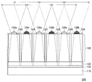
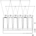
- 1 is a schematic cross-sectional view illustrating a configuration of an imaging apparatus according to an embodiment of the present disclosure. 1 is a schematic cross-sectional view illustrating a configuration of an imaging apparatus according to an embodiment of the present disclosure.
- FIG. 2 is a schematic cross-sectional view illustrating an example in which the arrangement interval of the openings (translucent portions) of the light shielding body is simply narrowed with respect to the configuration of FIG.
- FIG. 6 it is a schematic diagram which shows a mode that another image is acquired with each micro lens.
- FIG. 1 is a schematic cross-sectional view illustrating a configuration that is a premise of an imaging apparatus according to an embodiment of the present disclosure.
- the imaging apparatus 100 is used for imaging biological information such as a fingerprint, for example, as in the imaging apparatus 200 according to the present embodiment described later.
- the imaging device 100 includes a light receiving element layer 110, a light shielding body 120, a thin film bonding resin layer 130, a lower side light shielding layer 125, an upper side light shielding layer 126, and a cover glass 127.
- the imaging device 100 is formed by bonding a light receiving element layer 110 and a light shielding body 120 by a thin film bonding resin layer 130.
- a thin film bonding resin layer 130 By bonding the light receiving element layer 110 and the light blocking body 120 with the thin film bonding resin layer 130 without a gap, it is possible to prevent dew condensation that may have occurred in the gap, and to suppress deterioration of the obtained image.
- the light receiving element layer 110 is composed of a large number of light receiving elements arranged vertically and horizontally.
- the thin film bonding resin layer 130 is made of a transparent material, and is disposed in order to bond the light receiving element layer 110 and the light shielding body 120 without gaps.
- the light shielding body 120 includes a light shielding wall 122 made of a light shielding material such as Si, and a light transmitting portion 124 made of a transparent material such as glass or resin.
- the light shielding wall 122 is formed by opening a through hole in the light shielding material by processing such as lithography and dry etching.
- the translucent part 124 is formed by filling a transparent material between the light shielding walls 122 (that is, the through hole).
- the opening surrounded by the light shielding wall 122 is used as the light transmitting portion 124, and light incident from the upper side (light incident surface side) is transmitted to the lower side (light receiving element side). It is formed as follows.
- the lower side of the light shielding body 120 is made of a light shielding material such as BLK CF (black color filter), Ti, W or the like, and more than each opening of the light shielding body 120 (the translucent part 124 surrounded by the light shielding wall 122).
- a lower side light shielding layer 125 having a narrow rectangular opening is formed.
- An upper side light shielding layer 126 made of a light shielding material such as CF, Ti, W, etc., having a circular opening narrower than each opening of the light shielding body 120 (translucent portion 124 surrounded by the light shielding wall 122) is formed. Yes.
- a microlens 128 is formed in the circular opening of the upper side light shielding layer 126.
- a cover glass 127 is disposed on the subject side of the micro lens 128.
- a user's finger is placed on the cover glass 127 and illuminated from the side by an LED or the like.
- light is scattered in the finger, and information such as fingerprints and veins can be acquired by causing the internal scattered light to enter the imaging apparatus 100 and imaging.
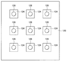
- FIG. 2 is a schematic diagram illustrating a state in which the imaging apparatus 100 is viewed from above in FIG.
- the upper side light shielding layer 126 is not shown.
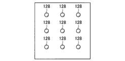
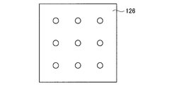
- 3 to 5 are schematic views showing the microlens 128, the upper side light shielding layer 126, and the lower side light shielding layer 125 when the imaging apparatus 200 is viewed from above in FIG.
- FIG. 3 shows the arrangement of the microlenses 128,
- FIG. 4 shows the arrangement of the openings (circular portions) of the upper side light shielding layer 126, and FIG. (Rectangular part) arrangement.
- a portion of the photoelectric conversion region (pixel region) of the light receiving element layer 110 disposed under each opening of the light shielding body 120 contributes to photoelectric conversion and is effectively utilized.
- the region of the light receiving element layer 100 disposed under the non-opening portion of the light shielding body 120 is an invalid region that does not contribute to photoelectric conversion because incident light is shielded. Therefore, assuming that the ratio of the area contributing to photoelectric conversion to the area of the pixel region of the light receiving element layer 110 is the sensor area efficiency, the sensor area efficiency is low in the configuration example shown in FIGS. For this reason, in order to obtain desired performance and function as the imaging apparatus 100, it is necessary to expand the sensor area, which causes an increase in cost.
- FIGS. 1 to 5 the opening portion of the light shielding body 120 is also provided in the non-opening portion of the light shielding body 120, so Improve. 6 and 7 are schematic cross-sectional views illustrating the configuration of the imaging apparatus 200 according to an embodiment of the present disclosure.
- FIG. 8 is a schematic diagram illustrating a state in which the imaging apparatus 100 is viewed from above in FIGS. 6 and 7.
- the upper side light shielding layer 126 is not shown.
- 9 and 10 are schematic diagrams showing the upper side light shielding layer 126 and the lower side light shielding layer 125 when the imaging device 200 is viewed from above in FIGS. 6 and 7.
- FIG. 8 is a schematic diagram illustrating a state in which the imaging apparatus 100 is viewed from above in FIGS. 6 and 7.
- 9 and 10 are schematic diagrams showing the upper side light shielding layer 126 and the lower side light shielding layer 125 when the imaging device 200 is viewed from above in FIGS. 6 and 7.
- FIG. 8 shows the arrangement of the microlens 128 and the light transmitting portion 124
- FIG. 9 shows the arrangement of the opening (circular portion) of the upper side light shielding layer 126
- FIG. 10 shows the lower side light shielding layer. The arrangement of 125 openings (rectangular portions) is shown.
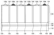
- FIG. 6 shows a cross section taken along the alternate long and short dash line I-I 'shown in FIG. 8
- FIG. 7 shows a cross section taken along the alternate long and short dash line II-II' shown in FIG.
- the light shielding body is also provided in the region where the opening (translucent portion 124) of the light shielding body 120 is not provided in the configurations of FIGS. 120 openings (translucent portion 124) are provided.
- FIGS. 8 to 10 show regions having the same area as FIGS. As is apparent from a comparison between FIG. 2 and FIG. 8, in FIG. 2, nine microlenses 128 and nine light transmitting portions 124 are provided, whereas in FIG. 36 light portions 124 are provided. If the ratio (length direction) of the light-shielding body opening to the non-opening in the configuration of FIGS.
- the sensor area efficiency of the structure of the present embodiment can be increased up to about 4 times. Compared with the case where the same function is realized by the configuration of FIGS. 1 to 5, the cost can be reduced to about 1 ⁇ 4.
- the sensor area efficiency can be further increased by further increasing the number of microlenses 128 and light transmitting portions 124. Further, if the sensor area efficiency is increased up to about 4 times, the area of the light receiving element layer 110 can be reduced to about 1/4 in order to obtain the same amount of information, so that the manufacturing cost can be greatly reduced. It is.
- the imaging apparatus 200 of this embodiment shown in FIGS. 6 to 10 has a structure in which optical elements such as lenses having different functions are alternately arranged to acquire different image information.
- the microlens 128a for green wavelength, the microlens 128b for red wavelength, the microlens 128c for blue wavelength, and the pinhole 129 are alternately arranged.
- the microlenses 128a, 128b, and 128c whose shapes and materials are optimized for each wavelength and the monochrome pinholes 129 are alternately arranged.
- the imaging area on the object side does not change, but the amount of information obtained without the influence of crosstalk in front of the lens can be dramatically increased (doubled only with the columns in this figure).
- the wavelength of light to be irradiated When acquiring biological information, it is desirable to change the wavelength of light to be irradiated according to the measurement target. For example, when measuring a fingerprint or a pulse, a green wavelength (about 570 nm) is used. Moreover, when measuring transparency, a pulse, and melanin, a red wavelength (about 660 nm) is used. In the case of measuring subcutaneous fat thickness, veins, and melanin, the near infrared wavelength (940) is used. Since the degree of refraction of light varies depending on the wavelength, the microlenses 128a, 128b, and 128c designed for each wavelength can be obtained by optimizing the lens shape of the microlenses 128a, 128b, and 128c according to the wavelength.
- Incident light can be acquired via By using the micro lenses 128a, 128b, and 128c corresponding to the wavelength of light, the amount of information obtained from the subject can be significantly increased. In addition, by making light incident through the pinhole 129, it is possible to directly acquire the luminance information of the subject.
- FIG. 11 is a schematic cross-sectional view showing an example in which the arrangement interval of the openings (translucent portion 124) of the light shield 120, that is, the arrangement interval of the microlenses 128 is simply narrowed with respect to the configuration of FIG.
- the arrangement interval of the openings (translucent portions 124) of the light shielding body 120 is simply narrowed, it seems that the pixel area of the light receiving element layer 110 can be effectively used. Since the imaging area on the side does not change, the amount of information obtained by the light receiving element layer 110 does not change greatly. In the area A shown in FIG.
- the opening (translucent portion 124) of the light shielding body 120 is spaced at a predetermined interval so that the imaging regions of the adjacent microlenses 128 do not overlap. Be placed. For this reason, in the area
- a new translucent part 124 is provided around the translucent part 124 already provided in the configuration example shown in FIGS. 1 to 5, and each translucent part 124 has a different function.
- each translucent part 124 has a different function.
- different image data is acquired in each region of the light receiving element layer 110 corresponding to each light transmitting portion 124. Therefore, the region of the light receiving element layer 110 that has not been used in the configuration examples of FIGS. 1 to 5 can be effectively used, and the sensor area efficiency can be greatly improved.
- FIG. 12 is a schematic diagram showing how different images are acquired by the microlens 128a and the microlens 128b in the configuration of the present embodiment shown in FIG.
- FIG. 12 by arranging the microlens 128a for green wavelength and the microlens 128b for red wavelength alternately, different images can be acquired by the microlens 128a and the microlens 128b, respectively. .
- the obtained information increases and the pixel region of the light receiving element layer 110 can be used effectively.
- FIG. 13 is a schematic cross-sectional view showing an example in which microlenses 128d and 128e having different optical magnifications are alternately arranged.
- the micro lenses 128d and 128e having different optical magnifications are arranged in a staggered manner in a plan view.
- images having the same imaging area and resolution can be acquired for subjects with different subject distances (focus positions).
- the configuration example shown in FIG. 13 is useful for acquiring a plurality of pieces of image information having different object distance (depth) directions. For example, when obtaining biometric information of a finger, the fingerprint and sweat glands are on the surface of the skin, while the vein is at a position about several millimeters deep from the surface of the skin.
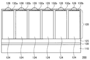
- FIG. 14 and 15 are schematic views showing an example in which different polarizers 132a and 132b are added below the microlens 128, and the polarizers 132a and 132b are alternately arranged.
- FIG. 15 is a schematic diagram illustrating a state viewed from above in FIG. 14, and is a schematic diagram illustrating an arrangement of the polarizers 132 a and 132 b.
- FIG. 14 corresponds to a cross section taken along one-dot chain line III-III ′ shown in FIG.
- the horizontal polarizer 132a and the vertical polarizer 132b are alternately arranged in the row along the alternate long and short dash line III-III ′ and in the two rows above and below the two rows. ing.
- the polarizers 132a and 132b are disposed at positions corresponding to the respective light transmitting portions 124.
- the ⁇ / 4 plate 134 and the opening 136 having no polarizer are alternately arranged in the row along the alternate long and short dash line III-III 'and in the row one row above and one row below.
- the ⁇ / 4 plate 134 and the opening 136 are also arranged at positions corresponding to the respective light transmitting portions 124.
- the ⁇ / 4 plate 134 (quarter wavelength plate) is a kind of polarizer.
- the incident light is linearly polarized light, it is converted into circularly polarized light (elliptical polarized light), and conversely, the incident light is circularly polarized ( In the case of elliptical polarized light, it has a function of converting to linearly polarized light.
- the light receiving element layer 110 can acquire polarized light according to the polarizer 132a, the polarizer 132b, and the ⁇ / 4 plate 134. . Therefore, also in the configuration shown in FIG. 15, different functions can be given to the adjacent light transmitting portions 124.
- FIGS. 16 to 18 are schematic cross-sectional views showing a configuration example in which the wavelength selection filter 140 is provided corresponding to each light transmitting portion 124.
- the wavelength selection filter 140 includes an organic material containing at least one of a pigment or a dye or a laminate of inorganic films.
- FIG. 16 is a schematic cross-sectional view showing an example in which a wavelength selection filter is provided below the microlens 128.
- FIG. 17 is a schematic cross-sectional view showing an example in which the wavelength selection filter 140 is provided at the same depth position as the lower side light shielding layer 125.
- FIG. 18 is a schematic cross-sectional view showing an example in which a wavelength selection filter is provided on the light receiving element layer 110.
- FIGS. 16 to 18 by providing at least one wavelength selection filter 140 in some microlenses 128, a plurality of wavelength data can be simultaneously acquired from the plurality of microlenses 128.
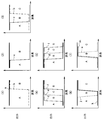
- FIG. 19 is a schematic diagram showing specific characteristics of the wavelength selection filter 140.
- the wavelength selective filter can be configured by combining a plurality of filter characteristics a to m.
- Each characteristic (1) to (7) of the wavelength selection filter 140 shown in FIG. 18 shows the relationship between the wavelength and the output.
- the characteristic a indicates the relationship between the wavelength and the output when the wavelength selection filter 140 is not used.
- the filter characteristics b to m the relationship between the wavelength and the output is different.
- the characteristics (1) to (7) of the wavelength selection filter can be obtained by combining the filter characteristics a to m.
- the wavelength selection filter 140 that transmits only wavelengths corresponding to the areas A and C is configured by combining the filter characteristics b and the filter characteristics c.
- the wavelength selective filter 140 can be configured. As described above, by arranging the wavelength selection filter 140 having different characteristics in each light transmitting portion 124 in which the microlens 128 is disposed, each adjacent light transmitting portion 124 can have a different function.
- image information that has passed through different optical elements for each adjacent light transmitting portion 124 is acquired in the light receiving element layer 110.
- the microlenses 128a to 128f, the pinhole 129, the polarizers 132a and 132b, and the wavelength selection filter 140 described above correspond to optical elements.
- the present embodiment more information can be obtained from the region corresponding to each light transmitting portion 124 of the light receiving element layer 110.
- the sensor area efficiency can be greatly improved by reducing the non-opening portion of the light shielding body 120 disposed below the microlens 128 to prevent crosstalk as much as possible.
- optical components such as lenses having different functions are alternately arranged for each adjacent light transmitting portion 124, and different image information is acquired. It is possible to dramatically increase the amount of information obtained without the influence of crosstalk in front of the lens.
- a light shielding body having a light shielding wall and a plurality of light transmitting portions formed in a plurality of openings between the light shielding walls; A large number of light receiving elements that perform photoelectric conversion according to incident light input through the light transmitting portion of the light blocking body are arranged, and image information that has passed through different optical elements for each of the adjacent light transmitting portions is acquired.
- a light receiving element layer An imaging apparatus comprising: (2) The optical element is a microlens provided for each light-transmitting portion on the light incident surface side of the light shielding body, The imaging device according to (1), wherein the light receiving element layer includes the light receiving element that performs photoelectric conversion according to incident light that is condensed by the microlens and input through the light transmitting unit. (3) The imaging device according to (2), wherein the microlenses corresponding to the adjacent translucent portions have different shapes according to the wavelength of incident light. (4) The imaging device according to (2), wherein the microlens corresponding to the adjacent translucent part has different optical magnifications according to the subject distance.
- the imaging device according to (2) wherein, in the adjacent light-transmitting portions, one light-transmitting portion is provided with a pinhole as the optical element instead of the microlens.
- the optical element according to (1) wherein the optical element is a wavelength conversion filter that is provided in the adjacent translucent part and converts a wavelength so that the wavelength of incident light is different for each adjacent translucent part.
- Imaging device. (7) A first light-shielding layer formed on the light incident surface side of the light-shielding body and having an opening for each opening of the light-shielding body, The imaging device according to (6), wherein the wavelength conversion filter is provided in the vicinity of the first light shielding layer.
- a second light-shielding layer that is formed on the light-receiving element layer side of the light-shielding body and has an opening for each opening of the light-shielding body
- the optical element is a polarizer that is provided in the adjacent light-transmitting part and controls the polarization direction so that the polarization direction of incident light is different for each adjacent light-transmitting part. The imaging device described.
- a first light-shielding layer formed on the light incident surface side of the light-shielding body and having an opening for each opening of the light-shielding body,
Landscapes
- Physics & Mathematics (AREA)
- General Physics & Mathematics (AREA)
- Optics & Photonics (AREA)
- Engineering & Computer Science (AREA)
- Multimedia (AREA)
- Signal Processing (AREA)
- Solid State Image Pick-Up Elements (AREA)
- Transforming Light Signals Into Electric Signals (AREA)
- Life Sciences & Earth Sciences (AREA)
- Sustainable Development (AREA)
- Sustainable Energy (AREA)
- Facsimile Heads (AREA)
Abstract
【課題】受光素子のセンサ領域を有効活用すること。 【解決手段】本開示に係る撮像装置は、遮光壁と前記遮光壁間の複数の開口部に形成された複数の透光部を有する遮光体と、前記遮光体の前記透光部を介して入力された入射光に応じて光電変換を行う多数の受光素子が配列され、隣接する前記透光部毎に異なる光学素子を通過した画像情報を取得する受光素子層と、を備える。この構成により、隣接する透光部毎に異なる光学素子を通過した画像情報が取得されるため、受光素子のセンサ領域を有効活用すること。
Description
本開示は、撮像装置に関する。
従来、例えばイメージセンサにおけるレンズ下方のクロストーク防止する構造として、下記の特許文献1に記載された技術が公知である。特許文献1には、複数の受光部をもつ光電変換素子と、該受光部ごとに形成されたマイクロレンズとからなるイメージセンサにおいて、前記光電変換素子と前記マイクロレンズとで挟まれた領域に、前記受光部ごとに光の入射方向を制限する遮光壁が、前記光電変換素子上に一体的に形成された構成が記載されている。
しかし、上記特許文献に記載された技術では、隣接するマイクロレンズによって撮像される被写体領域には重複が生じる場合がある。このため、光電変換素子のセンサ面積を有効に活用できない問題が生じる。
そこで、受光素子層のセンサ領域を有効活用することが求められていた。
本開示によれば、遮光壁と前記遮光壁間の複数の開口部に形成された複数の透光部を有する遮光体と、前記遮光体の前記透光部を介して入力された入射光に応じて光電変換を行う多数の受光素子が配列され、隣接する前記透光部の領域毎に異なる種類の画像情報を取得する受光素子層と、を備える、撮像装置が提供される。
以上説明したように本開示によれば、受光素子のセンサ領域を有効活用することが求められていた。
なお、上記の効果は必ずしも限定的なものではなく、上記の効果とともに、または上記の効果に代えて、本明細書に示されたいずれかの効果、または本明細書から把握され得る他の効果が奏されてもよい。
なお、上記の効果は必ずしも限定的なものではなく、上記の効果とともに、または上記の効果に代えて、本明細書に示されたいずれかの効果、または本明細書から把握され得る他の効果が奏されてもよい。
以下に添付図面を参照しながら、本開示の好適な実施の形態について詳細に説明する。なお、本明細書及び図面において、実質的に同一の機能構成を有する構成要素については、同一の符号を付することにより重複説明を省略する。
なお、説明は以下の順序で行うものとする。
1.前提となる構成例
2.本開示に係る撮像装置の構成例
1.前提となる構成例
2.本開示に係る撮像装置の構成例
1.前提となる構成例
図1は、本開示の一実施形態に係る撮像装置の前提となる構成を示す概略断面図である。この撮像装置100は、後述する本実施形態に係る撮像装置200と同様、例えば指紋などの生体情報を撮像するために用いられる。撮像装置100は、受光素子層110、遮光体120、薄膜接合樹脂層130、下辺遮光層125、上辺遮光層126、カバーガラス127を有して構成されている。
図1は、本開示の一実施形態に係る撮像装置の前提となる構成を示す概略断面図である。この撮像装置100は、後述する本実施形態に係る撮像装置200と同様、例えば指紋などの生体情報を撮像するために用いられる。撮像装置100は、受光素子層110、遮光体120、薄膜接合樹脂層130、下辺遮光層125、上辺遮光層126、カバーガラス127を有して構成されている。
撮像装置100は、受光素子層110と遮光体120が薄膜接合樹脂層130により接合されて形成される。受光素子層110と遮光体120を薄膜接合樹脂層130により隙間なく接合することにより、その隙間に起こり得た結露を防止することができ、得られる画像の劣化を抑止することができる。
受光素子層110は、縦横に配置された多数の受光素子から成る。薄膜接合樹脂層130は、透明材から成り、受光素子層110と遮光体120を隙間なく接合するために配置される。
遮光体120は、Siなどの遮光材から成る遮光壁122と、ガラスまたは樹脂などの透明材から成る透光部124から構成される。遮光壁122は、遮光材に対してリソグラフィとドライエッチングなどの加工によって貫通孔を開口することにより形成される。透光部124は、遮光壁122の間(すなわち、貫通孔)に透明材が充填されることにより形成される。
すなわち、遮光体120は、遮光壁122によって囲まれている開口部が透光部124とされ、上辺側(光の入射面側)から入射される光を下辺側(受光素子側)に透過させるように形成されている。
遮光体120の下辺側には、BLK CF(黒色カラーフィルタ)やTi,Wなどの遮光材から成り、遮光体120の各開口部(遮光壁122によって囲まれている透光部124)よりも狭い矩形の開口部を有する下辺遮光層125が形成されている。
一方、遮光体120の上辺側には、BLK
CFやTi,Wなどの遮光材から成り、遮光体120の各開口部(遮光壁122によって囲まれている透光部124)よりも狭い円形の開口部を有する上辺遮光層126が形成されている。上辺遮光層126の円形の開口部には、マイクロレンズ128が形成されている。また、マイクロレンズ128よりも被写体側にはカバーガラス127が配置されている。
CFやTi,Wなどの遮光材から成り、遮光体120の各開口部(遮光壁122によって囲まれている透光部124)よりも狭い円形の開口部を有する上辺遮光層126が形成されている。上辺遮光層126の円形の開口部には、マイクロレンズ128が形成されている。また、マイクロレンズ128よりも被写体側にはカバーガラス127が配置されている。
被写体からの光は、マイクロレンズ128、上辺遮光層126、透光部124、下辺遮光層125を通過し、最終的に図5に示す下辺遮光層125の開口に対応する矩形(正方形)の光として受光素子層110に入射する。
生体情報として例えば指紋の情報を取得する際には、ユーザの指がカバーガラス127の上に置かれ、横からLED等により照明を当てる。これにより、光が指の中で散乱し、この内部散乱光を撮像装置100に入射させて撮像することで、指紋、静脈などの情報を取得することができる。
図2は、図1の上方から撮像装置100を見た状態を示す模式図である。図2では、上辺遮光層126の図示は省略している。また、図3~図5は、図2の上方から撮像装置200を見た場合のマイクロレンズ128、上辺遮光層126、下辺遮光層125を示す模式図である。ここで、図3は、マイクロレンズ128の配置を示しており、図4は、上辺遮光層126の開口部(円形部分)の配置を示しており、図5は下辺遮光層125の開口部(矩形部分)の配置を示している。
図1~図5に示した構成において、受光素子層110の光電変換領域(画素領域)のうち遮光体120の各開口部下に配置される部分は光電変換に寄与して有効に活用される。一方、遮光体120の非開口部下に配置される受光素子層100の領域は、入射光が遮蔽されるため光電変換に寄与しない無効領域となる。このため、受光素子層110の画素領域の面積に対する光電変換に寄与する面積の比率をセンサ面積効率とすると、図1~図5に示す構成例では、センサ面積効率が低くなる。このため、撮像装置100として所望の性能・機能を得るためにはセンサ面積を拡げる必要があり、コストアップ要因となる。
2.本開示に係る撮像装置の構成例
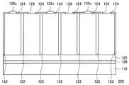
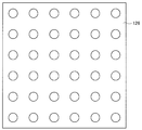
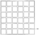
本実施形態では、図1~図5に示す構成では遮光体120の非開口部となっている部分にも遮光体120の開口部を設け、センサ面積効率を向上させる。図6及び図7は、本開示の一実施形態に係る撮像装置200の構成を示す概略断面図である。また、図8は、図6及び図7の上方から撮像装置100を見た状態を示す模式図である。図8では、上辺遮光層126の図示は省略している。また、図9、図10は、図6及び図7の上方から撮像装置200を見た場合の上辺遮光層126、下辺遮光層125を示す模式図である。ここで、図8は、マイクロレンズ128及び透光部124の配置を示しており、図9は、上辺遮光層126の開口部(円形部分)の配置を示しており、図10は下辺遮光層125の開口部(矩形部分)の配置を示している。
本実施形態では、図1~図5に示す構成では遮光体120の非開口部となっている部分にも遮光体120の開口部を設け、センサ面積効率を向上させる。図6及び図7は、本開示の一実施形態に係る撮像装置200の構成を示す概略断面図である。また、図8は、図6及び図7の上方から撮像装置100を見た状態を示す模式図である。図8では、上辺遮光層126の図示は省略している。また、図9、図10は、図6及び図7の上方から撮像装置200を見た場合の上辺遮光層126、下辺遮光層125を示す模式図である。ここで、図8は、マイクロレンズ128及び透光部124の配置を示しており、図9は、上辺遮光層126の開口部(円形部分)の配置を示しており、図10は下辺遮光層125の開口部(矩形部分)の配置を示している。
また、図6は、図8に示す一点鎖線I-I’に沿った断面を示しており、図7は、図8に示す一点鎖線II-II’に沿った断面を示している。
図6~図10に示すように、本実施形態に係る撮像装置200では、図1~図5の構成では遮光体120の開口部(透光部124)が設けられていない領域にも遮光体120の開口部(透光部124)を設けている。ここで、図8~図10は、図2~図5と同じ面積の領域を示している。図2と図8を比較すると明らかなように、図2ではマイクロレンズ128及び透光部124が9個設けられているのに対し、図8では、図2と同じ面積にマイクロレンズ128及び透光部124が36個設けられている。図1~図5の構成における遮光体開口部と非開口部の比(長さ方向)が1:1であれば、本実施形態の構造のセンサ面積効率は最大4倍近くまで高めることができ、図1~図5の構成で同じ機能を実現する場合に比べ、コストを1/4近くに抑制することができる。なお、図2においてマイクロレンズ128及び透光部124の数を更に増やすことで、センサ面積効率を更に高めることが可能である。また、センサ面積効率が4倍程度まで上昇すれば、同じ情報量を取得するためには、受光素子層110の面積を1/4程度まで縮小できるため、製造コストを大幅に低減することも可能である。
図6~図10に示す本実施形態の撮像装置200では、異なる機能を持つレンズ等の光学素子を交互に配置し、それぞれ異なる画像情報を取得する構造としている。具体的には、図6~図8に示すように、緑波長用のマイクロレンズ128a、赤波長用のマイクロレンズ128b、青波長用のマイクロレンズ128c、及びピンホール129が交互に配置される。このように、本実施形態では、波長ごとに形状や材質等を最適化したマイクロレンズ128a,128b,128cと、モノクロ用のピンホール129を交互に配置する。これにより、物体側の撮像領域は変わらないが、レンズ前方のクロストークの影響なく得られる情報量を飛躍的(この図の列だけで2倍)に増やすことができる。
生体情報を取得する際には、測定対象に応じて照射する光の波長を変えることが望ましい。例えば、指紋や脈拍を測定する場合には、緑波長(570nm程度)を用いる。また、透明度、脈拍、メラニンを測定する場合には、赤波長(660nm程度)を用いる。また、皮下脂肪厚、静脈、メラニンを測定する場合には、近赤外波長(940)を用いる。光は波長に応じて屈折の度合いが変わるため、波長に応じてマイクロレンズ128a,128b,128cのレンズ形状を最適化することで、それぞれの波長に合った設計のマイクロレンズ128a,128b,128cを介して入射光を取得することができる。そして、光の波長に応じたマイクロレンズ128a,128b,128cを用いることで、被写体から得られる情報量を大幅に増大することが可能である。また、ピンホール129を介して光を入射させることで、被写体の輝度情報を直接取得することが可能となる。
図11は、図1の構成に対して、遮光体120の開口部(透光部124)の配置間隔、すなわち、マイクロレンズ128の配置間隔を単純に狭くした例を示す概略断面図である。図11に示すように、単純に遮光体120の開口部(透光部124)の配置間隔を狭くした場合、受光素子層110の画素領域を有効に活用できるように見えるが、実際には物体側の撮像領域は変わらないため、受光素子層110で得られる情報量に大きな変化はない。図11に示す領域Aでは、隣接するマイクロレンズ128の撮像領域が重なるため、同じ情報を余分に取得することになり、透光部124の配置間隔を狭くしても情報量を増やすことはできない。むしろ、図11に示す構成では、各開口部への入射光にはレンズ前方(上方)のクロストークが生じ、得られた情報の信号処理に大きな負荷がかかるため、コストアップ要因となる。
従って、図1~図5に示した構成例のように、遮光体120の開口部(透光部124)は、隣接するマイクロレンズ128の撮像領域が重ならないように、所定の間隔を空けて配置される。このため、遮光体120の開口部が設けられていない領域では、下層の受光素子層100が利用されないため、センサ面積効率が低下してしまう。
一方、本実施形態では、図1~図5に示した構成例で既に設けられている透光部124の周囲に新たな透光部124を設け、各透光部124に異なる機能を持たせることで、各透光部124に対応する受光素子層110の各領域が異なる画像データを取得する。従って、図1~図5の構成例では使用されていなかった受光素子層110の領域を有効活用することができ、センサ面積効率を大幅に向上することが可能である。
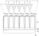
図12は、図6に示す本実施形態の構成において、マイクロレンズ128aとマイクロレンズ128bのそれぞれで別の画像が取得される様子を示す模式図である。図12に示すように、緑波長用のマイクロレンズ128aと赤波長用のマイクロレンズ128bとを交互に配置することで、マイクロレンズ128aとマイクロレンズ128bのそれぞれで別の画像を取得することができる。これにより、得られる情報が増えると共に、受光素子層110の画素領域を有効に活用することが可能となる。
図13は、光学倍率の異なるマイクロレンズ128d,128eを交互に配置した例を示す概略断面図である。光学倍率の異なるマイクロレンズ128d,128eは、平面的には千鳥状に配置される。図13に示す構成によれば、異なる被写体距離(ピント位置)の被写体に対し、同じ撮像領域と解像度を持つ画像を取得することができる。図13に示す構成例は、物体距離(深さ)方向が異なる複数の画像情報の取得に有用である。例えば指の生体情報を取得する場合、指紋や汗腺は皮膚の表面にある一方、静脈は皮膚の表面から数mm程度深い位置にある。図13に示す構成例によれば、これらの深さの異なる生体情報を同時に取得することが可能である。一方、図1~図5に示す構成例では、光学倍率が等しいマイクロレンズ128を複数設けているため、例えば指の指紋にピントを合わせた場合は、静脈は合焦位置から外れるため、静脈の情報を取得することはできない。このように、本実施形態によれば、各透光部124のマイクロレンズ128d,128eの光学倍率を異ならせることで、各透光部124に対応する受光素子層110の各領域が異なる画像データを取得することができ、センサ面積効率を大幅に向上することが可能である。
以上説明した例では、マイクロレンズ128の特性を変えることで各透光部124に対応する受光素子層110の各領域が異なる画像データを取得するようにした。一方、マイクロレンズ128と受光素子層110の間に素子を設けることで、各透光部124に対応する受光素子層110の各領域が異なる画像データを取得するようにしても良い。
図14及び図15は、マイクロレンズ128の下部に異なる偏光子132a,132bを追加し、偏光子132a,132bを交互に配置した例を示す模式図である。図15は、図14の上方から見た状態を示す模式図であって、偏光子132a,132bの配置を示す模式図である。図14は、図15に示す一点鎖線III-III’に沿った断面に対応している。
図15に示すように、一点鎖線III-III’に沿った行と、その2行上、2行下の行では、水平方向の偏光子132aと垂直方向の偏光子132bとが交互に配置されている。偏光子132a,132bは、各透光部124に対応する位置に配置される。また、一点鎖線III-III’に沿った行と、その1行上、1行下の行では、λ/4板134と偏光子を有していない開口部136が交互に配置されている。λ/4板134と開口部136も、各透光部124に対応する位置に配置される。λ/4板134(四分の一波長板)は、偏光子の一種であり、入射光が直線偏光だった場合は円偏光(楕円偏光)に変換し、また逆に入射光が円偏光(楕円偏光)だった場合は直線偏光に変換する機能を有している。
従って、偏光子132a,偏光子132b、λ/4板134が設けられた領域では、偏光子132a,偏光子132b、λ/4板134に応じた偏光を受光素子層110が取得することができる。従って、図15に示す構成においても、隣接する各透光部124で異なる機能を持たせることができる。
また、図16~図18は、各透光部124に対応して波長選択フィルタ140を設けた構成例を示す概略断面図である。波長選択フィルタ140は、一例として、顔料もしくは染料の少なくとも一つを含む有機材料、もしくは、無機膜の積層から構成される。ここで、図16は、マイクロレンズ128の下に波長選択フィルタを設けた例を示す概略断面図である。また、図17は、下辺遮光層125と同じ深さ位置に波長選択フィルタ140を設けた例を示す概略断面図である。また、図18は、受光素子層110の上に波長選択フィルタを設けた例を示す概略断面図である。図16~図18に示すように、一部のマイクロレンズ128に、少なくとも1つの波長選択フィルタ140を設けることにより、複数のマイクロレンズ128から複数の波長データを同時に取得できる。
図19は、波長選択フィルタ140の具体的な特性を示す模式図である。波長選択フィルタは、複数のフィルタ特性a~mを組み合わせて構成することができる。図18に示す波長選択フィルタ140の各特性(1)~(7)は、波長と出力との関係を示している。各特性(1)~(7)において、aの特性は、波長選択フィルタ140を用いない場合の、波長と出力の関係を示している。また、フィルタ特性b~mのそれぞれでは、波長と出力の関係が異なっている。フィルタ特性a~mを組み合わせることで、波長選択フィルタの各特性(1)~(7)を得ることができる。例えば、特性(3)では、フィルタ特性bとフィルタ特性cを組み合わせることで、領域Aと領域Cに相当する波長のみを透過させる波長選択フィルタ140を構成している。また、特性(4)、特性(5)では、フィルタ特性d~f、特性g~iの組み合わせを適宜変更することで、短波長側から長波長側の領域A~Dを通過又は遮断する任意の波長選択フィルタ140を構成することができる。このように、特性の異なる波長選択フィルタ140をマイクロレンズ128が配置された各透光部124に配置することで、隣接する各透光部124で異なる機能を持たせることができる。
以上のように、本実施形態では、隣接する透光部124毎に異なる光学素子を通過した画像情報が、受光素子層110において取得される。ここで、上述したマイクロレンズ128a~128f、ピンホール129、偏光子132a,132b、波長選択フィルタ140が光学素子に相当する。
これにより、本実施形態によれば、受光素子層110の各透光部124に対応する領域からより多くの情報を得ることができる。そして、マイクロレンズ128の下方にクロストーク防止のために配置する遮光体120の非開口部を極力削減することにより、センサ面積効率を大幅に向上させることが可能となる。また、異なる機能を持つレンズ等の光学部品を隣接する透光部124毎に交互に配置し、それぞれ異なる画像情報を取得する構造とすることで。レンズ前方のクロストークの影響なく得られる情報量を飛躍的に増やすことが可能となる。
以上、添付図面を参照しながら本開示の好適な実施形態について詳細に説明したが、本開示の技術的範囲はかかる例に限定されない。本開示の技術分野における通常の知識を有する者であれば、特許請求の範囲に記載された技術的思想の範疇内において、各種の変更例または修正例に想到し得ることは明らかであり、これらについても、当然に本開示の技術的範囲に属するものと了解される。
また、本明細書に記載された効果は、あくまで説明的または例示的なものであって限定的ではない。つまり、本開示に係る技術は、上記の効果とともに、または上記の効果に代えて、本明細書の記載から当業者には明らかな他の効果を奏しうる。
なお、以下のような構成も本開示の技術的範囲に属する。
(1) 遮光壁と前記遮光壁間の複数の開口部に形成された複数の透光部を有する遮光体と、
前記遮光体の前記透光部を介して入力された入射光に応じて光電変換を行う多数の受光素子が配列され、隣接する前記透光部毎に異なる光学素子を通過した画像情報を取得する受光素子層と、
を備える、撮像装置。
(2) 前記光学素子は、前記遮光体の光の入射面側に前記透光部毎に設けられているマイクロレンズであり、
前記受光素子層は、前記マイクロレンズにより集光されて前記透光部を介して入力された入射光に応じて光電変換を行う前記受光素子を備える、前記(1)に記載の撮像装置。
(3) 隣接する前記透光部に対応する前記マイクロレンズは、入射光の波長に応じた異なる形状を有する、前記(2)に記載の撮像装置。
(4) 隣接する前記透光部に対応する前記マイクロレンズは、被写体距離に応じた異なる光学倍率を有する、前記(2)に記載の撮像装置。
(5) 隣接する前記透光部において、1の前記透光部には前記マイクロレンズの代わりに前記光学素子としてピンホールが設けられる、前記(2)に記載の撮像装置。
(6) 前記光学素子は、隣接する前記透光部に設けられ、隣接する前記透光部毎に入射光の波長が異なるように波長を変換する波長変換フィルタである、前記(1)に記載の撮像装置。
(7) 前記遮光体の光の入射面側に形成され、前記遮光体の前記開口部毎に開口部を有する第1の遮光層を備え、
前記波長変換フィルタは、前記第1の遮光層の近傍に設けられた、前記(6)に記載の撮像装置。
(8) 前記遮光体の受光素子層側に形成され、前記遮光体の前記開口部毎に開口部を有する第2の遮光層を備え、
前記波長変換フィルタは、前記第2の遮光層の近傍に設けられた、前記(6)に記載の撮像装置。
(9) 前記波長変換フィルタは、前記受光素子層の表面に設けられた、前記(6)に記載の撮像装置。
(10) 前記光学素子は、隣接する前記透光部に設けられ、隣接する前記透光部毎に入射光の偏光方向が異なるように偏光方向を制御する偏光子である、前記(1)に記載の撮像装置。
(11) 前記遮光体の光の入射面側に形成され、前記遮光体の前記開口部毎に開口部を有する第1の遮光層を備え、
前記偏光子は、前記第1の遮光層の近傍に設けられた、前記(10)に記載の撮像装置。
(1) 遮光壁と前記遮光壁間の複数の開口部に形成された複数の透光部を有する遮光体と、
前記遮光体の前記透光部を介して入力された入射光に応じて光電変換を行う多数の受光素子が配列され、隣接する前記透光部毎に異なる光学素子を通過した画像情報を取得する受光素子層と、
を備える、撮像装置。
(2) 前記光学素子は、前記遮光体の光の入射面側に前記透光部毎に設けられているマイクロレンズであり、
前記受光素子層は、前記マイクロレンズにより集光されて前記透光部を介して入力された入射光に応じて光電変換を行う前記受光素子を備える、前記(1)に記載の撮像装置。
(3) 隣接する前記透光部に対応する前記マイクロレンズは、入射光の波長に応じた異なる形状を有する、前記(2)に記載の撮像装置。
(4) 隣接する前記透光部に対応する前記マイクロレンズは、被写体距離に応じた異なる光学倍率を有する、前記(2)に記載の撮像装置。
(5) 隣接する前記透光部において、1の前記透光部には前記マイクロレンズの代わりに前記光学素子としてピンホールが設けられる、前記(2)に記載の撮像装置。
(6) 前記光学素子は、隣接する前記透光部に設けられ、隣接する前記透光部毎に入射光の波長が異なるように波長を変換する波長変換フィルタである、前記(1)に記載の撮像装置。
(7) 前記遮光体の光の入射面側に形成され、前記遮光体の前記開口部毎に開口部を有する第1の遮光層を備え、
前記波長変換フィルタは、前記第1の遮光層の近傍に設けられた、前記(6)に記載の撮像装置。
(8) 前記遮光体の受光素子層側に形成され、前記遮光体の前記開口部毎に開口部を有する第2の遮光層を備え、
前記波長変換フィルタは、前記第2の遮光層の近傍に設けられた、前記(6)に記載の撮像装置。
(9) 前記波長変換フィルタは、前記受光素子層の表面に設けられた、前記(6)に記載の撮像装置。
(10) 前記光学素子は、隣接する前記透光部に設けられ、隣接する前記透光部毎に入射光の偏光方向が異なるように偏光方向を制御する偏光子である、前記(1)に記載の撮像装置。
(11) 前記遮光体の光の入射面側に形成され、前記遮光体の前記開口部毎に開口部を有する第1の遮光層を備え、
前記偏光子は、前記第1の遮光層の近傍に設けられた、前記(10)に記載の撮像装置。
110 受光素子層
120 遮光体
122 遮光壁
128,128a~128e マイクロレンズ
129 ピンホール
132a,132b 偏光子
140 波長選択フィルタ
200 撮像装置
120 遮光体
122 遮光壁
128,128a~128e マイクロレンズ
129 ピンホール
132a,132b 偏光子
140 波長選択フィルタ
200 撮像装置
Claims (11)
- 遮光壁と前記遮光壁間の複数の開口部に形成された複数の透光部を有する遮光体と、
前記遮光体の前記透光部を介して入力された入射光に応じて光電変換を行う多数の受光素子が配列され、隣接する前記透光部毎に異なる光学素子を通過した画像情報を取得する受光素子層と、
を備える、撮像装置。 - 前記光学素子は、前記遮光体の光の入射面側に前記透光部毎に設けられているマイクロレンズであり、
前記受光素子層は、前記マイクロレンズにより集光されて前記透光部を介して入力された入射光に応じて光電変換を行う前記受光素子を備える、請求項1に記載の撮像装置。 - 隣接する前記透光部に対応する前記マイクロレンズは、入射光の波長に応じた異なる形状を有する、請求項2に記載の撮像装置。
- 隣接する前記透光部に対応する前記マイクロレンズは、被写体距離に応じた異なる光学倍率を有する、請求項2に記載の撮像装置。
- 隣接する前記透光部において、1の前記透光部には前記マイクロレンズの代わりに前記光学素子としてピンホールが設けられる、請求項2に記載の撮像装置。
- 前記光学素子は、隣接する前記透光部に設けられ、隣接する前記透光部毎に入射光の波長が異なるように波長を変換する波長変換フィルタである、請求項1に記載の撮像装置。
- 前記遮光体の光の入射面側に形成され、前記遮光体の前記開口部毎に開口部を有する第1の遮光層を備え、
前記波長変換フィルタは、前記第1の遮光層の近傍に設けられた、請求項6に記載の撮像装置。 - 前記遮光体の受光素子層側に形成され、前記遮光体の前記開口部毎に開口部を有する第2の遮光層を備え、
前記波長変換フィルタは、前記第2の遮光層の近傍に設けられた、請求項6に記載の撮像装置。 - 前記波長変換フィルタは、前記受光素子層の表面に設けられた、請求項6に記載の撮像装置。
- 前記光学素子は、隣接する前記透光部に設けられ、隣接する前記透光部毎に入射光の偏光方向が異なるように偏光方向を制御する偏光子である、請求項1に記載の撮像装置。
- 前記遮光体の光の入射面側に形成され、前記遮光体の前記開口部毎に開口部を有する第1の遮光層を備え、
前記偏光子は、前記第1の遮光層の近傍に設けられた、請求項10に記載の撮像装置。
Priority Applications (1)
| Application Number | Priority Date | Filing Date | Title |
|---|---|---|---|
| US16/318,458 US10917546B2 (en) | 2016-07-29 | 2017-06-06 | Imaging device utilizing sensor area of photoelectric conversion elements corresponding to incident light passed through optical elements including a layer of polarizers of horizontal and vertical directions and quarter wave plates |
Applications Claiming Priority (2)
| Application Number | Priority Date | Filing Date | Title |
|---|---|---|---|
| JP2016150039A JP2018019020A (ja) | 2016-07-29 | 2016-07-29 | 撮像装置 |
| JP2016-150039 | 2016-07-29 |
Publications (1)
| Publication Number | Publication Date |
|---|---|
| WO2018020846A1 true WO2018020846A1 (ja) | 2018-02-01 |
Family
ID=61015887
Family Applications (1)
| Application Number | Title | Priority Date | Filing Date |
|---|---|---|---|
| PCT/JP2017/021011 Ceased WO2018020846A1 (ja) | 2016-07-29 | 2017-06-06 | 撮像装置 |
Country Status (3)
| Country | Link |
|---|---|
| US (1) | US10917546B2 (ja) |
| JP (1) | JP2018019020A (ja) |
| WO (1) | WO2018020846A1 (ja) |
Cited By (6)
| Publication number | Priority date | Publication date | Assignee | Title |
|---|---|---|---|---|
| JP2020021041A (ja) * | 2018-08-03 | 2020-02-06 | 采▲ぎょく▼科技股▲ふん▼有限公司VisEra Technologies Company Limited | 光学素子およびその製造方法 |
| CN111328398A (zh) * | 2019-08-23 | 2020-06-23 | 深圳市汇顶科技股份有限公司 | 指纹识别装置和电子设备 |
| CN111801679A (zh) * | 2019-07-12 | 2020-10-20 | 深圳市汇顶科技股份有限公司 | 指纹检测装置和电子设备 |
| US11417143B2 (en) | 2019-08-23 | 2022-08-16 | Shenzhen GOODIX Technology Co., Ltd. | Fingerprint detection apparatus and method and electronic device |
| PT12142U (pt) * | 2022-05-10 | 2022-11-10 | Afonso Gondar Marques Dos Santos Tiago | Êmbolo visuo-tátil |
| US11804509B2 (en) | 2019-10-18 | 2023-10-31 | Shenzhen GOODIX Technology Co., Ltd. | Fingerprint detection apparatus and electronic device |
Families Citing this family (7)
| Publication number | Priority date | Publication date | Assignee | Title |
|---|---|---|---|---|
| US10529763B2 (en) * | 2018-04-19 | 2020-01-07 | Semiconductor Components Industries, Llc | Imaging pixels with microlenses |
| FR3094140B1 (fr) * | 2019-03-22 | 2022-04-08 | Isorg | Capteur d'images comprenant un filtre angulaire |
| KR20220035438A (ko) * | 2019-07-23 | 2022-03-22 | 쓰리엠 이노베이티브 프로퍼티즈 컴파니 | 마이크로렌즈 및 차광 구조체를 포함하는 광학 시스템 |
| CN113707676B (zh) * | 2020-05-22 | 2024-11-26 | 格科微电子(上海)有限公司 | 光学指纹器件的制造方法 |
| JP7518691B2 (ja) * | 2020-07-30 | 2024-07-18 | 株式会社ジャパンディスプレイ | 検出装置及び光フィルタ |
| CN114185170A (zh) * | 2020-09-14 | 2022-03-15 | 中强光电股份有限公司 | 近眼光场显示装置 |
| US12397732B2 (en) | 2021-09-24 | 2025-08-26 | Mitsubishi Electric Corporation | Illumination control device, biometric information acquiring device, and illumination control method |
Citations (9)
| Publication number | Priority date | Publication date | Assignee | Title |
|---|---|---|---|---|
| JPH0738075A (ja) * | 1993-07-23 | 1995-02-07 | Nec Corp | 固体撮像装置 |
| JPH08102924A (ja) * | 1994-09-30 | 1996-04-16 | Sharp Corp | 画像入出力装置 |
| JPH09116127A (ja) * | 1995-10-24 | 1997-05-02 | Sony Corp | 固体撮像装置 |
| JP2001061109A (ja) * | 1999-08-20 | 2001-03-06 | Japan Science & Technology Corp | 画像入力装置 |
| JP2001223846A (ja) * | 2000-02-10 | 2001-08-17 | Sharp Corp | イメージセンサおよびその製造方法 |
| JP2006196634A (ja) * | 2005-01-13 | 2006-07-27 | Matsushita Electric Ind Co Ltd | カラー固体撮像装置の製造方法 |
| JP2007121631A (ja) * | 2005-10-27 | 2007-05-17 | Funai Electric Co Ltd | 複眼撮像装置 |
| JP2007158825A (ja) * | 2005-12-06 | 2007-06-21 | Ricoh Co Ltd | 画像入力装置 |
| WO2016009707A1 (ja) * | 2014-07-16 | 2016-01-21 | ソニー株式会社 | 複眼撮像装置 |
Family Cites Families (3)
| Publication number | Priority date | Publication date | Assignee | Title |
|---|---|---|---|---|
| EP2452228A4 (en) * | 2009-07-10 | 2015-06-03 | Front Street Invest Man Inc As Manager For Front Street Diversified Income Class | METHOD AND APPARATUS FOR GENERATING THREE DIMENSIONAL IMAGE INFORMATION USING A SINGLE D IMAGING COURSE |
| JP5446797B2 (ja) * | 2009-12-04 | 2014-03-19 | 株式会社リコー | 撮像装置 |
| WO2016037063A1 (en) * | 2014-09-05 | 2016-03-10 | Massachusetts Institute Of Technology | Systems, methods, and apparatus for sensitive thermal imaging |
-
2016
- 2016-07-29 JP JP2016150039A patent/JP2018019020A/ja active Pending
-
2017
- 2017-06-06 US US16/318,458 patent/US10917546B2/en not_active Expired - Fee Related
- 2017-06-06 WO PCT/JP2017/021011 patent/WO2018020846A1/ja not_active Ceased
Patent Citations (9)
| Publication number | Priority date | Publication date | Assignee | Title |
|---|---|---|---|---|
| JPH0738075A (ja) * | 1993-07-23 | 1995-02-07 | Nec Corp | 固体撮像装置 |
| JPH08102924A (ja) * | 1994-09-30 | 1996-04-16 | Sharp Corp | 画像入出力装置 |
| JPH09116127A (ja) * | 1995-10-24 | 1997-05-02 | Sony Corp | 固体撮像装置 |
| JP2001061109A (ja) * | 1999-08-20 | 2001-03-06 | Japan Science & Technology Corp | 画像入力装置 |
| JP2001223846A (ja) * | 2000-02-10 | 2001-08-17 | Sharp Corp | イメージセンサおよびその製造方法 |
| JP2006196634A (ja) * | 2005-01-13 | 2006-07-27 | Matsushita Electric Ind Co Ltd | カラー固体撮像装置の製造方法 |
| JP2007121631A (ja) * | 2005-10-27 | 2007-05-17 | Funai Electric Co Ltd | 複眼撮像装置 |
| JP2007158825A (ja) * | 2005-12-06 | 2007-06-21 | Ricoh Co Ltd | 画像入力装置 |
| WO2016009707A1 (ja) * | 2014-07-16 | 2016-01-21 | ソニー株式会社 | 複眼撮像装置 |
Cited By (10)
| Publication number | Priority date | Publication date | Assignee | Title |
|---|---|---|---|---|
| JP2020021041A (ja) * | 2018-08-03 | 2020-02-06 | 采▲ぎょく▼科技股▲ふん▼有限公司VisEra Technologies Company Limited | 光学素子およびその製造方法 |
| CN110794497A (zh) * | 2018-08-03 | 2020-02-14 | 采钰科技股份有限公司 | 光学元件及其制造方法 |
| US10684400B2 (en) | 2018-08-03 | 2020-06-16 | Visera Technologies Company Limited | Optical elements and method for fabricating the same |
| CN110794497B (zh) * | 2018-08-03 | 2024-07-30 | 采钰科技股份有限公司 | 光学元件及其制造方法 |
| CN111801679A (zh) * | 2019-07-12 | 2020-10-20 | 深圳市汇顶科技股份有限公司 | 指纹检测装置和电子设备 |
| CN111801679B (zh) * | 2019-07-12 | 2024-04-30 | 深圳市汇顶科技股份有限公司 | 指纹检测装置和电子设备 |
| CN111328398A (zh) * | 2019-08-23 | 2020-06-23 | 深圳市汇顶科技股份有限公司 | 指纹识别装置和电子设备 |
| US11417143B2 (en) | 2019-08-23 | 2022-08-16 | Shenzhen GOODIX Technology Co., Ltd. | Fingerprint detection apparatus and method and electronic device |
| US11804509B2 (en) | 2019-10-18 | 2023-10-31 | Shenzhen GOODIX Technology Co., Ltd. | Fingerprint detection apparatus and electronic device |
| PT12142U (pt) * | 2022-05-10 | 2022-11-10 | Afonso Gondar Marques Dos Santos Tiago | Êmbolo visuo-tátil |
Also Published As
| Publication number | Publication date |
|---|---|
| JP2018019020A (ja) | 2018-02-01 |
| US10917546B2 (en) | 2021-02-09 |
| US20190297234A1 (en) | 2019-09-26 |
Similar Documents
| Publication | Publication Date | Title |
|---|---|---|
| WO2018020846A1 (ja) | 撮像装置 | |
| CN111095286B (zh) | 指纹检测装置和电子设备 | |
| CN111801688B (zh) | 光学指纹装置和电子设备 | |
| CN110945524B (zh) | 识别指纹的方法、指纹识别装置和电子设备 | |
| KR102098657B1 (ko) | 디스플레이 일체형 지문센서를 갖는 전자기기, 그것의 사용자 인증 방법, 및 그것의 사용자 지문 등록 방법 | |
| US10735634B2 (en) | Image capture apparatus | |
| CN108140125A (zh) | 光学指纹成像系统和面阵传感器 | |
| WO2018153070A1 (zh) | 光学指纹识别装置和显示面板 | |
| CN111108511A (zh) | 指纹检测装置和电子设备 | |
| US11544958B2 (en) | Light detection apparatus and application thereof | |
| CN111108510B (zh) | 指纹检测装置和电子设备 | |
| JPWO2015015717A1 (ja) | 撮像装置、並びにそれを用いた撮像システム、電子ミラーシステムおよび測距装置 | |
| CN111108509B (zh) | 指纹检测装置和电子设备 | |
| CN110858299A (zh) | 生物识别传感器及具备其的显示装置 | |
| WO2021008088A1 (zh) | 指纹检测装置和电子设备 | |
| JPWO2016208403A1 (ja) | イメージセンサ、および電子機器 | |
| CN210605739U (zh) | 指纹检测装置和电子设备 | |
| WO2021146976A1 (zh) | 指纹检测的装置和电子设备 | |
| JP2012117867A (ja) | 光学装置及び電子機器 | |
| CN211319244U (zh) | 指纹检测的装置和电子设备 | |
| WO2021007730A1 (zh) | 指纹检测装置和电子设备 | |
| WO2021007953A1 (zh) | 指纹检测装置和电子设备 | |
| CN211787124U (zh) | 生物识别成像装置和电子装置 | |
| WO2022071862A1 (en) | Biometric imaging arrangement for infrared imaging comprising microlenses | |
| CN111095287B (zh) | 光学指纹装置和电子设备 |
Legal Events
| Date | Code | Title | Description |
|---|---|---|---|
| 121 | Ep: the epo has been informed by wipo that ep was designated in this application |
Ref document number: 17833856 Country of ref document: EP Kind code of ref document: A1 |
|
| NENP | Non-entry into the national phase |
Ref country code: DE |
|
| 122 | Ep: pct application non-entry in european phase |
Ref document number: 17833856 Country of ref document: EP Kind code of ref document: A1 |