WO2018016430A1 - Combined inspection system - Google Patents
Combined inspection system Download PDFInfo
- Publication number
- WO2018016430A1 WO2018016430A1 PCT/JP2017/025676 JP2017025676W WO2018016430A1 WO 2018016430 A1 WO2018016430 A1 WO 2018016430A1 JP 2017025676 W JP2017025676 W JP 2017025676W WO 2018016430 A1 WO2018016430 A1 WO 2018016430A1
- Authority
- WO
- WIPO (PCT)
- Prior art keywords
- sample
- ray
- unit
- inspection
- inspection apparatus
- Prior art date
Links
Images


Classifications
-
- G—PHYSICS
- G01—MEASURING; TESTING
- G01N—INVESTIGATING OR ANALYSING MATERIALS BY DETERMINING THEIR CHEMICAL OR PHYSICAL PROPERTIES
- G01N23/00—Investigating or analysing materials by the use of wave or particle radiation, e.g. X-rays or neutrons, not covered by groups G01N3/00 – G01N17/00, G01N21/00 or G01N22/00
- G01N23/20—Investigating or analysing materials by the use of wave or particle radiation, e.g. X-rays or neutrons, not covered by groups G01N3/00 – G01N17/00, G01N21/00 or G01N22/00 by using diffraction of the radiation by the materials, e.g. for investigating crystal structure; by using scattering of the radiation by the materials, e.g. for investigating non-crystalline materials; by using reflection of the radiation by the materials
- G01N23/20008—Constructional details of analysers, e.g. characterised by X-ray source, detector or optical system; Accessories therefor; Preparing specimens therefor
- G01N23/20025—Sample holders or supports therefor
-
- G—PHYSICS
- G01—MEASURING; TESTING
- G01N—INVESTIGATING OR ANALYSING MATERIALS BY DETERMINING THEIR CHEMICAL OR PHYSICAL PROPERTIES
- G01N23/00—Investigating or analysing materials by the use of wave or particle radiation, e.g. X-rays or neutrons, not covered by groups G01N3/00 – G01N17/00, G01N21/00 or G01N22/00
- G01N23/20—Investigating or analysing materials by the use of wave or particle radiation, e.g. X-rays or neutrons, not covered by groups G01N3/00 – G01N17/00, G01N21/00 or G01N22/00 by using diffraction of the radiation by the materials, e.g. for investigating crystal structure; by using scattering of the radiation by the materials, e.g. for investigating non-crystalline materials; by using reflection of the radiation by the materials
- G01N23/201—Investigating or analysing materials by the use of wave or particle radiation, e.g. X-rays or neutrons, not covered by groups G01N3/00 – G01N17/00, G01N21/00 or G01N22/00 by using diffraction of the radiation by the materials, e.g. for investigating crystal structure; by using scattering of the radiation by the materials, e.g. for investigating non-crystalline materials; by using reflection of the radiation by the materials by measuring small-angle scattering
-
- G—PHYSICS
- G01—MEASURING; TESTING
- G01N—INVESTIGATING OR ANALYSING MATERIALS BY DETERMINING THEIR CHEMICAL OR PHYSICAL PROPERTIES
- G01N23/00—Investigating or analysing materials by the use of wave or particle radiation, e.g. X-rays or neutrons, not covered by groups G01N3/00 – G01N17/00, G01N21/00 or G01N22/00
- G01N23/20—Investigating or analysing materials by the use of wave or particle radiation, e.g. X-rays or neutrons, not covered by groups G01N3/00 – G01N17/00, G01N21/00 or G01N22/00 by using diffraction of the radiation by the materials, e.g. for investigating crystal structure; by using scattering of the radiation by the materials, e.g. for investigating non-crystalline materials; by using reflection of the radiation by the materials
- G01N23/20008—Constructional details of analysers, e.g. characterised by X-ray source, detector or optical system; Accessories therefor; Preparing specimens therefor
- G01N23/20016—Goniometers
-
- G—PHYSICS
- G01—MEASURING; TESTING
- G01N—INVESTIGATING OR ANALYSING MATERIALS BY DETERMINING THEIR CHEMICAL OR PHYSICAL PROPERTIES
- G01N23/00—Investigating or analysing materials by the use of wave or particle radiation, e.g. X-rays or neutrons, not covered by groups G01N3/00 – G01N17/00, G01N21/00 or G01N22/00
- G01N23/20—Investigating or analysing materials by the use of wave or particle radiation, e.g. X-rays or neutrons, not covered by groups G01N3/00 – G01N17/00, G01N21/00 or G01N22/00 by using diffraction of the radiation by the materials, e.g. for investigating crystal structure; by using scattering of the radiation by the materials, e.g. for investigating non-crystalline materials; by using reflection of the radiation by the materials
- G01N23/203—Measuring back scattering
-
- G—PHYSICS
- G01—MEASURING; TESTING
- G01N—INVESTIGATING OR ANALYSING MATERIALS BY DETERMINING THEIR CHEMICAL OR PHYSICAL PROPERTIES
- G01N21/00—Investigating or analysing materials by the use of optical means, i.e. using sub-millimetre waves, infrared, visible or ultraviolet light
- G01N21/84—Systems specially adapted for particular applications
- G01N21/88—Investigating the presence of flaws or contamination
- G01N21/95—Investigating the presence of flaws or contamination characterised by the material or shape of the object to be examined
- G01N21/9501—Semiconductor wafers
-
- G—PHYSICS
- G01—MEASURING; TESTING
- G01N—INVESTIGATING OR ANALYSING MATERIALS BY DETERMINING THEIR CHEMICAL OR PHYSICAL PROPERTIES
- G01N2223/00—Investigating materials by wave or particle radiation
- G01N2223/045—Investigating materials by wave or particle radiation combination of at least 2 measurements (transmission and scatter)
-
- G—PHYSICS
- G01—MEASURING; TESTING
- G01N—INVESTIGATING OR ANALYSING MATERIALS BY DETERMINING THEIR CHEMICAL OR PHYSICAL PROPERTIES
- G01N2223/00—Investigating materials by wave or particle radiation
- G01N2223/05—Investigating materials by wave or particle radiation by diffraction, scatter or reflection
- G01N2223/054—Investigating materials by wave or particle radiation by diffraction, scatter or reflection small angle scatter
-
- G—PHYSICS
- G01—MEASURING; TESTING
- G01N—INVESTIGATING OR ANALYSING MATERIALS BY DETERMINING THEIR CHEMICAL OR PHYSICAL PROPERTIES
- G01N2223/00—Investigating materials by wave or particle radiation
- G01N2223/10—Different kinds of radiation or particles
- G01N2223/101—Different kinds of radiation or particles electromagnetic radiation
- G01N2223/1016—X-ray
-
- G—PHYSICS
- G01—MEASURING; TESTING
- G01N—INVESTIGATING OR ANALYSING MATERIALS BY DETERMINING THEIR CHEMICAL OR PHYSICAL PROPERTIES
- G01N2223/00—Investigating materials by wave or particle radiation
- G01N2223/30—Accessories, mechanical or electrical features
- G01N2223/304—Accessories, mechanical or electrical features electric circuits, signal processing
-
- G—PHYSICS
- G01—MEASURING; TESTING
- G01N—INVESTIGATING OR ANALYSING MATERIALS BY DETERMINING THEIR CHEMICAL OR PHYSICAL PROPERTIES
- G01N2223/00—Investigating materials by wave or particle radiation
- G01N2223/30—Accessories, mechanical or electrical features
- G01N2223/321—Accessories, mechanical or electrical features manipulator for positioning a part
-
- G—PHYSICS
- G01—MEASURING; TESTING
- G01N—INVESTIGATING OR ANALYSING MATERIALS BY DETERMINING THEIR CHEMICAL OR PHYSICAL PROPERTIES
- G01N2223/00—Investigating materials by wave or particle radiation
- G01N2223/60—Specific applications or type of materials
- G01N2223/611—Specific applications or type of materials patterned objects; electronic devices
- G01N2223/6116—Specific applications or type of materials patterned objects; electronic devices semiconductor wafer
-
- H—ELECTRICITY
- H01—ELECTRIC ELEMENTS
- H01L—SEMICONDUCTOR DEVICES NOT COVERED BY CLASS H10
- H01L22/00—Testing or measuring during manufacture or treatment; Reliability measurements, i.e. testing of parts without further processing to modify the parts as such; Structural arrangements therefor
- H01L22/10—Measuring as part of the manufacturing process
- H01L22/12—Measuring as part of the manufacturing process for structural parameters, e.g. thickness, line width, refractive index, temperature, warp, bond strength, defects, optical inspection, electrical measurement of structural dimensions, metallurgic measurement of diffusions
Definitions
- the present invention relates to a composite inspection system suitable for a technical field of manufacturing an element having a multilayer film structure in which a large number of thin films are laminated on a substrate, such as a semiconductor manufacturing field.
- the shape of this kind of processed element is called CD (Critical Dimension) as an important numerical value to be managed in the semiconductor process.
- TEMs transmission electron microscopes
- SEMs scanning electron microscopes
- an inspection apparatus for measuring the shape of the element as described above in-line in a non-destructive manner in a semiconductor manufacturing process an inspection apparatus using a scanning electron microscope (CD-SEM: Optical Dimension-Scanning Electron Microscope), an optical technique
- CD-SEM Optical Dimension-Scanning Electron Microscope
- OCD Optical Critical Dimension
- CD-AFM Critical Dimension Atomic Force Microscope
- an X-ray nano-shape measurement device (CD-SAXS: Critical Dimension Small Angle X-ray Scattering) using small-angle X-ray scattering has been proposed as an inspection device that accurately determines repeated pattern shapes using X-rays.
- Patent Documents 1 and 2 disclose conventional examples of CD-SAXS.
- the OCD described above has advantages such as a small measurement area and high throughput due to the use of light as a probe, and features that can analyze complex three-dimensional structures of semiconductor devices using modeling and simulation. Therefore, it is effective as an inspection apparatus for in-line measurement in the semiconductor manufacturing process.
- the CD-SEM is effective as an inspection apparatus for directly observing the device surface shape using the principle of a scanning electron microscope.
- these inspection apparatuses have a limit of resolution on a scale with a pitch of 10 nm or less, and analysis becomes difficult as the semiconductor elements are miniaturized.
- CD-SAXS is effective as an inspection device that analyzes the nanometer-scale shape of the surface of an electronic device.
- a powerful X-ray source is required, and a compact high-intensity X-ray source suitable for a semiconductor in-line inspection apparatus has not been obtained.
- the present invention has been made in view of the circumstances of these prior arts, and an object thereof is to provide a composite inspection system suitable for shape analysis of an element having a multilayer film structure in which a large number of thin films are laminated on a substrate, such as a semiconductor element. .
- Non-Patent Document 1 The basic concept of this type of combined inspection system is disclosed in Non-Patent Document 1, and the present invention is embodied based on this basic concept.
- the present invention includes a first inspection apparatus that inspects a sample based on X-ray measurement data obtained by irradiating the sample with X-rays, and a second inspection that inspects the sample by a measurement technique that does not use X-rays.
- a combined inspection system comprising: One of the X-ray measurement data obtained by the first inspection apparatus and the analysis result of the X-ray measurement data is output to the second inspection apparatus, The second inspection apparatus is characterized by inspecting a sample by using one of the X-ray measurement data obtained by the first inspection apparatus and the analysis result of the X-ray measurement data.
- the first inspection apparatus is A measurement unit that irradiates the surface of the sample with X-rays and measures the scattering intensity;
- the fine structure on the surface of the sample forms a plurality of layers having different refractive indexes in a direction perpendicular to the surface, and a periodic structure in which unit structures are periodically arranged in a direction parallel to the surface in the layer.
- the scattering intensity of X-rays scattered by the fine structure was calculated, and the X-ray scattering intensity calculated by the sample model was measured.
- a fitting section for fitting to the scattering intensity A determination unit that determines an optimum value of a parameter for specifying the shape of the unit structure based on a fitting result of the fitting unit; An output unit that outputs at least part of an analysis value including an optimum value of a parameter that specifies the shape of the unit structure as an output value according to a predetermined protocol, and a second inspection apparatus,
- the second inspection apparatus can be configured to inspect the sample using the output value from the first inspection apparatus.
- the first inspection device A measurement unit that irradiates the surface of the sample with X-rays and measures the scattering intensity;
- the fine structure on the surface forms one or a plurality of layers in a direction perpendicular to the surface, and unit structures are periodically arranged in the layer in a direction parallel to the surface, and the unit structure Is assumed to have a sample model that constitutes a periodic structure that has random position fluctuations from a strict periodic position, and the position fluctuations are not dependent on mutual position differences, and are random.
- the unit structure is formed by uniform solid regions and spatial regions in the layer, the X-ray scattering intensity generated by the solid region is calculated, and the X-ray scattering intensity calculated by the sample model is measured.
- a fitting part to be fitted to A determination unit that determines an optimum value of a parameter for specifying the shape of the unit structure based on a fitting result of the fitting unit; An output unit that outputs at least part of an analysis value including an optimum value of a parameter that specifies the shape of the unit structure as an output value according to a predetermined protocol, and a second inspection apparatus,
- the second inspection apparatus may be configured to inspect the sample using an output value from the first inspection apparatus.
- position fluctuation refers to a deviation (variation) from a position (strict periodic position) where the unit structure should be.
- the “substance region” refers to a region where a substance (basically a solid) exists in the unit structure.
- the “space region” refers to a region where no substance (basically solid) exists in the unit structure. Gas is also present in the space region.
- the present invention also provides a first inspection apparatus that inspects a sample based on X-ray measurement data obtained by irradiating the sample with X-rays, and a second inspection that inspects the sample by a measurement technique that does not use X-rays.
- a combined inspection system including an inspection device, One of the measurement data obtained by the second inspection device and the analysis result of the measurement data is output to the first inspection device;
- the first inspection apparatus may be configured to inspect the sample using one of the measurement data obtained by the second inspection apparatus and the analysis result of the measurement data.
- the present invention also provides a first inspection apparatus for inspecting a sample based on X-ray measurement data obtained by irradiating the sample with X-rays, and a second inspection for inspecting the sample by a measurement technique not using X-rays.
- a combined inspection system comprising: The first inspection device A measurement unit that irradiates the surface of the sample with X-rays and measures the scattering intensity;
- the fine structure on the surface of the sample forms a plurality of layers having different refractive indexes in a direction perpendicular to the surface, and a periodic structure in which unit structures are periodically arranged in a direction parallel to the surface in the layer
- a sample model that constitutes Taking into account the effects of refraction and reflection caused by a plurality of layers formed in the sample model, the scattering intensity of X-rays scattered by the fine structure was calculated, and the X-ray scattering intensity calculated by the sample model was measured.
- a fitting section for fitting to the scattering intensity A determination unit that determines an optimum value of a parameter for specifying the shape of the unit structure based on a fitting result of the fitting unit; An output unit that outputs, as an output value, at least a part of an analysis value that includes an optimum value of a parameter that identifies the shape of the unit structure, and Using one of the X-ray measurement data obtained by the first inspection device and the analysis result of the X-ray measurement data, and one of the data obtained by the second inspection device and the analysis result of the data, It can also be set as the structure which analyzes the structure of a sample.
- the present invention provides a first inspection apparatus that inspects a sample based on X-ray measurement data obtained by irradiating the sample with X-rays, and a second inspection that inspects the sample by a measurement technique that does not use X-rays.
- a combined inspection system including an inspection device,
- the first inspection device A measurement unit that irradiates the surface of the sample with X-rays and measures the scattering intensity;
- the fine structure on the surface of the sample forms one or more layers in a direction perpendicular to the surface, and unit structures are periodically arranged in the direction parallel to the surface in the layer, and the unit
- the unit Assuming a sample model that constitutes a periodic structure in which the structure has a position fluctuation from a strict periodic position, and this position fluctuation does not depend on the position difference between each other, and is random.
- the unit structure is formed by uniform solid regions and spatial regions in the layer, the X-ray scattering intensity generated by the solid region is calculated, and the X-ray scattering intensity calculated by the sample model is measured.
- a fitting part to be fitted to A determination unit that determines an optimum value of a parameter for specifying the shape of the unit structure based on a fitting result of the fitting unit; An output unit that outputs at least a part of an analysis value including an optimum value of a parameter that specifies the shape of the unit structure according to a predetermined protocol, Using one of the X-ray measurement data obtained by the first inspection device and the analysis result of the X-ray measurement data, and one of the data obtained by the second inspection device and the analysis result of the data, It can also be set as the structure which analyzes the structure of a sample.
- the first inspection apparatus includes: A sample stage on which a sample to be inspected is placed; An image observation unit for observing an image of the sample placed on the sample stage; A positioning mechanism that is controlled based on the image observation result of the sample by the image observation unit and moves the sample stage in two directions orthogonal to each other on the horizontal plane, in the height direction, and in the in-plane rotation direction; First and second swiveling members that independently swivel around a rotation axis included in the same plane as the surface of the sample disposed on the sample stage and along a virtual plane perpendicular to the surface of the sample are included.
- Goniometer An X-ray irradiation unit that is mounted on the first turning member and collects and radiates characteristic X-rays to an inspection position set in the same plane as the surface of the sample placed on the sample stage;
- An X-ray detector mounted on the second swivel member;
- An analysis unit for digitizing and analyzing the X-ray pattern detected by the X-ray detector; It can be set as the structure provided with.
- the first inspection apparatus can be configured to measure X-rays transmitted through the sample by the X-ray detector, and measure scattered X-rays from the surface of the sample by the X-ray detector. It can also be configured. Specifically, a transmission-type small angle X-ray scattering (T-SAXS) that measures transmitted X-rays is used as the first inspection device, or the surface of the sample is smeared. A reflective small-angle X-ray scattering apparatus (GI-SAXS: Glazing Incidence-Small Angle X-ray Scattering) that measures X-rays scattered from the surface by entering X-rays at an angle can be used.
- T-SAXS transmission-type small angle X-ray scattering
- GI-SAXS Glazing Incidence-Small Angle X-ray Scattering
- GI-SAXS is suitable for measuring a line and space structure having a depth of 200 nm or less, and holes and protrusions
- T-SAXS is suitable for measuring a hole diameter of a structure having a depth of 200 nm or more, such as a hole structure.
- the first inspection apparatus may be configured to be capable of measuring both T-SAXS and GI-SAXS.
- the first inspection apparatus can be configured to include a two-dimensional X-ray detector as an X-ray detector. Thereby, quick measurement becomes possible.
- the second inspection apparatus can be constituted by, for example, an optical inspection apparatus (OCD).
- OCD optical inspection apparatus
- the second inspection apparatus may use an apparatus of another technique such as an inspection apparatus using a scanning electron microscope (CD-SEM) or an inspection apparatus using an atomic force microscope (CD-AFM). .
- CD-SEM scanning electron microscope
- CD-AFM atomic force microscope
- the analysis value output from the first inspection apparatus can be configured to include the pitch of the periodic structure in the sample model. More specifically, as the information (analysis value) transferred from the first inspection apparatus to the second inspection apparatus, various parameters can be used according to the shape of the surface. , Minimum line width (CD: Critical Dimension), height, sidewall angle (Side-Wall Angle), roundness (Roundness), etc., and variation information of each parameter is also included.
- the analysis value output from the first inspection apparatus may include the hole diameter.
- the combined inspection system of the present invention it is possible to analyze the element shape of a multilayer film structure in which a large number of thin films are stacked on a substrate, such as a semiconductor element, with high accuracy and multifaceted analysis. .
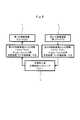
- FIG. 1 is a block diagram schematically showing a first basic configuration example and an information transmission system of a combined inspection system according to an embodiment of the present invention.
- FIG. 2 is a block diagram schematically showing a second basic configuration example and information transmission system of the combined inspection system according to the embodiment of the present invention.
- FIG. 3 is a block diagram schematically showing a third basic configuration example and an information transmission system of the combined inspection system according to the embodiment of the present invention.
- FIG. 4 is a block diagram schematically showing a fourth basic configuration example and an information transmission system of the combined inspection system according to the embodiment of the present invention.
- FIG. 5 is a block diagram schematically showing a fifth basic configuration example and information transmission system of the combined inspection system according to the embodiment of the present invention.
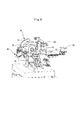
- FIG. 6 is a perspective view showing the overall structure of the first inspection apparatus according to the embodiment of the present invention.
- FIG. 7 is a front view of the first inspection apparatus shown in FIG.
- FIG. 8A is a side view schematically showing a configuration of an X-ray irradiation unit incorporated in the first inspection apparatus shown in FIG.
- FIG. 8B is a plan view of the same.
- FIG. 9 is a front view schematically showing another configuration example of the first inspection apparatus according to the embodiment of the present invention.
- FIG. 10 is a right side view schematically showing the configuration of the first inspection apparatus shown in FIG.
- FIG. 11 is a schematic diagram for explaining a measurement operation by the first inspection apparatus shown in FIG. FIG.
- FIG. 12A is a side view schematically showing the configuration of the X-ray irradiation unit incorporated in the first inspection apparatus shown in FIG.
- FIG. 12B is a plan view of the same.
- FIG. 13 is a block diagram showing a control system of the first inspection apparatus according to the embodiment of the present invention.
- FIG. 14 is a control flowchart of the first inspection apparatus according to the embodiment of the present invention.
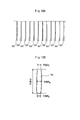
- FIG. 15A is a diagram showing parameters for analyzing the shape of the line and space pattern to be inspected.
- FIG. 15B is a diagram showing parameters for analyzing the shape of the line and space pattern created by the double exposure process.
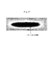
- FIG. 16A is a schematic cross-sectional view of a deep hole repeating structure to be inspected.
- FIG. 16A is a schematic cross-sectional view of a deep hole repeating structure to be inspected.
- FIG. 16B is an enlarged view of one deep hole in the schematic cross-sectional view shown in FIG. 16A.
- FIG. 17 is a diagram illustrating an example of measurement data obtained by a CD-SEM (second inspection apparatus).
- FIG. 18 is a diagram showing a usage example in which an observation image of a CD-SEM (second inspection apparatus) is fitted with a shape model of CD-SAXS (first inspection apparatus).
- FIGS. 1 to 5 are block diagrams schematically showing a basic configuration example and an information transmission system of a combined inspection system according to an embodiment of the present invention.
- the combined inspection system according to the present embodiment inspects a sample using a first inspection apparatus 1 that inspects the sample based on X-ray measurement data obtained by irradiating the sample with X-rays, and a measurement technique that does not use X-rays.
- the second inspection apparatus 2 is provided.
- the first inspection apparatus 1 for example, an X-ray nano shape measurement apparatus (CD-SAXS) is applied.
- the second inspection apparatus 2 for example, an optical inspection apparatus (OCD) or an inspection apparatus using a scanning electron microscope (CD-SEM) is applied.
- information from the first inspection apparatus 1 is output to the second inspection apparatus 2.
- information output from the first inspection apparatus 1 for example, in addition to measurement data obtained by X-ray measurement of a sample and the analysis result of the X-ray measurement data, information on the sample to be measured (Carrier, Wafer) Information).
- Carrier, Wafer information information on the sample to be measured.
- the OCD that constitutes the second inspection apparatus 2 uses light as a probe, it has advantages such as a small measurement area and a high throughput. Therefore, it is effective as an inspection device for in-line measurement in a semiconductor manufacturing process.
- OCD has a limit of resolution at a scale of 10 nm or less in pitch, and analysis becomes difficult as semiconductor elements are miniaturized.
- the CD-SAXS that constitutes the first inspection apparatus 1 is effective as an inspection apparatus that analyzes the nanometer-scale shape of the surface of the electronic device, and according to the configuration that includes an X-ray irradiation unit that will be described later, A small high-intensity X-ray source having a sufficiently powerful power for measuring a test pattern of 100 micrometers or less on the wafer surface can be obtained. Therefore, by using the information output from the first inspection apparatus 1, highly accurate analysis can be performed by the second inspection apparatus 2.
- Ethernet (Ethernet ⁇ registered trademark>) is used as a connection means
- any transmission method such as serial transmission such as RS-232C, optical transmission, or wireless transmission can be used.
- the first inspection device 1 and the second inspection device 2 are connected via the analysis server 3.
- the result of the first inspection device 1 is transmitted to the analysis server 3.
- the second inspection apparatus 2 obtains information from the analysis server 3.
- Ethernet registered trademark
- any transmission method such as serial transmission such as RS-232C, optical transmission, or wireless transmission can be used.
- the first inspection apparatus 1 and the second inspection apparatus 2 are connected via a host computer 4 (Host) that controls the process in a semiconductor factory.
- the result of the first inspection apparatus 1 is transmitted to the host computer 4 so that the second inspection apparatus 2 obtains information from the host computer 4.
- information is transmitted according to a standardized protocol called GEM300. If the host computer 4 is programmed, information transmission between the first and second inspection apparatuses 1 and 2 becomes possible.
- the first inspection device 1 and the second inspection device 2 are connected to the analysis server 3, and the analysis server 3 is further connected to the host computer 4. Yes.
- the analysis result of the first inspection device 1 and the measurement data of the second inspection device 2 are output to the analysis server 3, and the analysis server 3 outputs the analysis data from the second inspection device 2. Analysis of measurement data is executed. The analysis result is transmitted from the analysis server 3 to the host computer 4.
- information from the second inspection device 2 is output to the first inspection device 1.
- the first inspection apparatus 1 can perform highly accurate analysis.
- the first inspection device 1 and the second inspection device 2 are connected via a host computer 4 (Host) that controls the process in the semiconductor factory. Unlike the example, the result of the second inspection apparatus 2 is transmitted to the host computer 4. In a semiconductor manufacturing factory that normally uses a 300 mm wafer, information is transmitted according to a standardized protocol called GEM300. If the host computer 4 is programmed, information transmission between the first and second inspection apparatuses 1 and 2 becomes possible.
- OCD optical inspection apparatus
- the measurement / analysis procedure by OCD is as follows. First, prior to measurement, a large number of OCD-specific models into which parameters such as the detailed structure and material properties of the sample to be measured are input are created and stored as a library.
- a white light source is incident on the sample to be measured via a polarizer, light scattered by a fine pattern is detected by a spectroscope via an analyzer (spectral ellipsometer), and measurement
- a complex structure can be measured by combining several measurement techniques such as a method (reflectometer) in which light is incident directly above the target sample and the reflectance of the measurement target sample is measured.
- the spectrum waveform obtained by the measurement and the waveform calculated by the OCD model are compared, and the waveform waveform that most closely matches is determined as the shape of the measurement target sample. Based on this determination result, the shape is visualized and the dimensions of each part are output. The results obtained are fed back to model creation to improve analysis accuracy.
- OCD uses the analysis method as described above. Therefore, efficient measurement of dimensions is possible in the measurement range of the pattern that matches the model in the library, and it is applied as an in-line inspection of the semiconductor manufacturing process. Yes.
- OCD also has the following drawbacks. First, it takes a lot of time to create a library. In addition, it is necessary to prepare many actual samples for reference in order to create a library, which requires a lot of man-hours and costs.
- semiconductor miniaturization is progressing day by day, and if a fine pattern of 10 nm or less is measured, there is a limit of resolution coming from the wavelength range of incident light, and accurate dimension measurement becomes difficult.
- CD-SEM An inspection apparatus (CD-SEM) using a scanning electron microscope (SEM) is widely used in a semiconductor manufacturing line as a standard machine for measuring a two-dimensional dimension of a fine pattern in a semiconductor device.
- the measurement and analysis procedures using CD-SEM are as follows. That is, an SEM image is acquired for the measurement target sample, and the dimension of the measurement target sample is calculated from the image.
- the principle of image acquisition is the same as that of a normal SEM.
- An electron lens is used to focus an electron beam to a small diameter, scan the sample to be measured, and a secondary electron image and a reflected electron image emitted from the sample to be measured are obtained.
- An image is obtained by detection.
- the dimension calculation uses the contrast signal of the SEM image.
- the contrast distribution (line profile) of the location where the dimension is to be measured on the image is acquired, and the dimension of the measurement target sample is calculated from the line profile, the image magnification, and the number of pixels in the measurement section.
- CD-SEM has a merit that it has a deeper depth of focus than the optical type and can accurately measure the size of the bottom of the pattern.
- CD-SEM also has the following drawbacks. Depending on how the edge portion is taken from the line profile, the calculated dimension changes, so the reliability of the measurement result is low. Dimension measurement in the depth direction, where the electron beam may destroy the measurement target (especially organic matter such as resist), is not possible. Since CD-SEM has such drawbacks, there is a high possibility that it will not be able to cope with future semiconductor device manufacturing that will progress to further miniaturization and three-dimensionalization.
- FIG. 6 is a perspective view showing the entire structure of the first inspection apparatus
- FIG. 7 is a front view of the apparatus.
- the first inspection apparatus 1 includes an optical microscope 60 equipped with a sample stage 10, a positioning mechanism 20, a goniometer 30, an X-ray irradiation unit 40, an X-ray detector 50, a CCD camera, and the like.
- a semiconductor wafer (sample) to be inspected is disposed on the upper surface of the sample stage 10 and is driven by the positioning mechanism 20.
- the positioning mechanism 20 includes a horizontal movement mechanism that is movable in two perpendicular directions (X and Y directions) in a horizontal plane, a lifting mechanism that is movable in a vertical direction (Z direction) perpendicular to the horizontal plane, and an in-plane rotation mechanism.
- the sample stage 10 is moved in the X, Y, and Z directions and rotated in-plane so that an arbitrary measurement site on the semiconductor wafer disposed on the upper surface thereof is positioned in a predetermined direction to the irradiation X-ray convergence position. It has a function to do.
- the goniometer 30 includes first and second turning arms (turning members) 32 and 33 mounted on a goniometer body 31.
- the turning angle from the horizontal position of the first turning arm 32 is ⁇ S
- the turning angle from the horizontal position of the second turning arm 33 is ⁇ D
- the turning arms 32 and 33 are driven to turn.
- the first pivot arm 32 to pivot about the theta S axis, X-rays irradiation unit 40 are mounted. Further, the second pivot arm 33 to pivot about the theta D shaft are mounted the X-ray detector 50.
- the X-ray irradiation unit 40 has a function of condensing X-rays generated from the X-ray tube into characteristic X-rays having a specific wavelength and condensing them at one place.
- the position to which characteristic X-rays from the X-ray irradiation unit 40 are irradiated becomes the inspection position, and the measurement site of the sample arranged on the upper surface of the sample stage 10 is positioned to this inspection position by the positioning mechanism 20.
- the inspection position is set in the same plane as the surface of the sample placed on the sample stage 10.
- the X-ray detector 50 is used for X-ray reflectivity measurement (XRR) and small-angle X-ray scattering (SAXS) measurement.
- XRR X-ray reflectivity measurement
- SAXS small-angle X-ray scattering
- the film thickness and density are derived by measuring the interference between the reflected X-rays on the film surface and the reflected X-rays at the interface between the film and the substrate. Accuracy is obtained.
- the X-ray detector 50 for example, using a two-dimensional X-ray detector, X-ray reflectivity measurement in the TDI mode and small-angle X-ray scattering measurement in the Still mode can be performed.
- a measurement site of a sample (for example, a semiconductor wafer) arranged on the sample table 10 is arranged at a position below the optical microscope 60 by moving the sample table 10 by the positioning mechanism 20. Then, by moving in a horizontal direction from this position toward the inspection position, the measurement site of the sample (for example, a semiconductor wafer) is positioned at the inspection position.
- a sample for example, a semiconductor wafer
- FIG. 8A is a side view and FIG. 8B is a plan view.
- the X-ray irradiation unit 40 includes an X-ray tube 41, a first X-ray optical element 42, a second X-ray optical element 43, and a condensing slit 44.
- a condensing mirror having a multilayer film formed on the surface is used for the first and second X-ray optical elements 42 and 43.
- the unit body has a compact size and shape that can be mounted on the first swivel arm 32.
- the X-ray path will be described.
- the X-ray tube 41 an X-ray tube having an electron beam focal spot size on the target of ⁇ 100 ⁇ m or less, preferably 20 ⁇ m or less is used.
- the target material copper (Cu), molybdenum (Mo), silver (Ag), gold (Au), etc. can be selected, but small angle scattering having high angular resolution can be measured particularly when copper (Cu) is used. Is possible.
- X-rays emitted from the X-ray tube 41 first reach the first X-ray optical element 42. Then, the scattered X-ray 48 is condensed at the position of the X-ray detector 50 by the first X-ray optical element 42. As a result of focusing the scattered X-rays 48 on the X-ray detector 50 in this way, measurement with high angular resolution can be performed.
- the X-rays enter the second X-ray optical element 43, the light is collected in the vertical direction, and the incident X-rays 47 are collected on the surface of the sample 11. This also makes it possible to measure with high angular resolution when X-rays are grazingly incident on the surface of the sample 11 and X-ray reflectivity measurement or small-angle X-ray scattering measurement is performed.
- FIG. 9 is a front view schematically showing another configuration example of the first inspection apparatus, and FIG. 10 is a right side view of the same.
- the first inspection apparatus 1 shown in these drawings has a configuration suitable for a transmission-type small angle X-ray scattering apparatus (T-SAXS).
- the first inspection apparatus 1 shown in these drawings includes an optical microscope 60 equipped with a sample stage 10, a positioning mechanism 20, a goniometer 30, an X-ray irradiation unit 40, an X-ray detector 50, a CCD camera, and the like.
- the optical microscope 60 is omitted.
- a semiconductor wafer (sample) to be inspected is disposed on the upper surface of the sample stage 10 and is driven by the positioning mechanism 20.
- the positioning mechanism 20 includes a horizontal movement mechanism that is movable in two perpendicular directions (X and Y directions) in a horizontal plane, a lifting mechanism that is movable in a vertical direction (Z direction) perpendicular to the horizontal plane, and an in-plane rotation mechanism.
- the sample stage 10 is moved in the X, Y, and Z directions and rotated in-plane so that an arbitrary measurement site on the semiconductor wafer disposed on the upper surface thereof is positioned in a predetermined direction to the irradiation X-ray convergence position. It has a function to do.
- the goniometer 30 includes first and second turning arms (turning members) 32 and 33 mounted on a goniometer body 31.
- Each of the swivel arms 32 and 33 swivels around a virtual plane orthogonal to the upper surface of the sample table, with the axis ( ⁇ S axis, ⁇ D axis) perpendicular to the paper surface of FIG.
- the turning angle from the horizontal position of the first turning arm 32 is ⁇ S
- the turning angle from the horizontal position of the second turning arm 33 is ⁇ D
- the turning arms 32 and 33 are driven to turn.
- the first pivot arm 32 to pivot about the theta S axis, X-rays irradiation unit 40 are mounted. Further, the second pivot arm 33 to pivot about the theta D shaft are mounted the X-ray detector 50.
- the turning angle ⁇ S from the horizontal position of the first turning arm 32 can be driven to below the sample stage 10 (that is, ⁇ 90 °).
- transmission X-ray 49 as shown in FIG. 11 can be measured. Therefore, the first inspection apparatus 1 having such a configuration can be applied to a transmission-type small angle X-ray scattering apparatus (T-SAXS).
- T-SAXS transmission-type small angle X-ray scattering apparatus
- sample stage 10 and the positioning mechanism 20 need to transmit X-rays, they are formed of carbon, boron carbide, kapton, or the like having a small X-ray absorption coefficient, or as a cavity.
- FIG. 9 illustration of the positioning mechanism 20 and the support mechanism of the optical microscope 60 is omitted, but these support mechanisms are the swivel arms 32 and 33 of the goniometer, the X-ray irradiation unit 40, and the X-ray detector 50.
- the arrangement is such that it does not interfere with the surrounding components.
- FIG. 12A and 12B schematically show a configuration example of the X-ray irradiation unit 40 suitable when the first inspection apparatus 1 is configured by a transmission-type small angle X-ray scattering apparatus (T-SAXS).
- T-SAXS transmission-type small angle X-ray scattering apparatus
- the X-ray irradiation unit 40 shown in these drawings includes an X-ray tube 41, a first X-ray optical element 42, a second X-ray optical element 43, and a condensing slit 44 as constituent elements. .
- a condensing slit 44 as constituent elements.
- condensing mirrors having a multilayer film formed on the surface are used.
- These X-ray optical elements 42 and 43 have a structure enclosed in a housing not shown in order to prevent deterioration of the multilayer film.
- the housing has a mounting structure in which unnecessary stress is not applied so that the built-in X-ray optical elements 42 and 43 are not displaced or deformed.
- a position adjustment mechanism is provided so that high-precision alignment can be performed in each of the X-axis, Y-axis, and Z-axis directions.
- the X-ray tube 41 an X-ray tube having an electron beam focal spot size on the target of ⁇ 100 ⁇ m or less, preferably 20 ⁇ m or less is used.
- the target material copper (Cu), molybdenum (Mo), silver (Ag), gold (Au), etc. can be selected.
- Cu copper
- Mo molybdenum
- Au gold
- X-rays emitted from the X-ray tube 41 first reach the first X-ray optical element 42.
- the X-rays are collected in the horizontal direction (the direction parallel to the paper surface in FIG. 12B) by the first X-ray optical element 42 so that the position of the X-ray detector 50 is in focus.
- the light is condensed by the second X-ray optical element 43 in the vertical direction (in the direction parallel to the paper surface in FIG. 12A) so that the focus is similarly on the position of the X-ray detector 50.
- the condensed X-ray enters the measurement sample. X-rays are scattered by fine grooves and wirings formed in the measurement sample, pass through the sample, and reach the X-ray detector 50.
- a method of controlling the optical axis of the X-ray using the first and second X-ray optical elements 42 and 43 as described above is called a Kirkpatrick-Bayes method.
- the advantage of this method is that the two mirrors can be adjusted independently, so that the degree of freedom in controlling the shape of the focal point is high.
- this method although not shown, there is one in which two mirrors are integrated into an angle shape (L-shape), and this method may be used.
- This method of integrating two mirrors into an angle shape (L-shape) is called a side-by-side method, and it has advantages such as compactness of the optical system and easy alignment. Have.
- FIG. 13 is a block diagram showing a control system of the first inspection apparatus.
- the XG irradiation unit 40 is controlled by the XG controller 101.
- the sample image captured by the optical microscope 60 is recognized by the image recognition circuit 102.
- the optical microscope 60 and the image recognition circuit 102 constitute an image observation unit that observes an image of a sample placed on the sample stage 10. Note that the focus position of the optical microscope 60 is adjusted by the focus controller 103.
- the positioning controller 104 drives and controls the positioning mechanism 20 based on the sample image recognized by the optical microscope 60 and recognized by the image recognition circuit 102.
- the goniometer 30 is driven and controlled by the goniometer controller 106.
- the components of the XG controller 101, the image recognition circuit 102, the focus controller 103, the positioning controller 104, and the gonio controller 106 operate based on setting information sent from the central processing unit (CPU) 100, respectively.
- the setting information is stored in advance in the storage unit 110 as a recipe, and is read out by the central processing unit (CPU) 100 and output to the above-described components.
- the X-ray detector 50 is controlled by the count control circuit 107.
- the first inspection apparatus 1 also includes an operation unit 201 including a keyboard and a mouse for an operator to input various settings necessary for the operation of the apparatus. Further, the first inspection apparatus 1 includes a display unit 202 configured by a liquid crystal display or the like, and a communication unit 203 that executes data communication via a network.
- FIG. 14 is a flowchart showing an execution procedure of the X-ray thin film inspection method by the first inspection apparatus for inspecting a semiconductor wafer.
- Software for executing the X-ray thin film inspection is stored in the storage unit 110 in advance, and the central processing unit (CPU) 100 executes the following processing steps according to the software.
- the measurement site of the semiconductor wafer is positioned at the inspection position (step S1).
- unique points that can be specified by the image recognition circuit 102 based on image information from the optical microscope 60 are set in the storage unit 110 in advance as a recipe.
- the position information of the part to be measured is preset in the storage unit 110 as a recipe.
- a part that can be recognized by the image recognition circuit 102 without hesitation is set, such as a characteristic pattern shape formed on the surface of the semiconductor wafer.
- the image recognition circuit 102 recognizes and identifies the unique point set on the surface of the semiconductor wafer placed on the sample stage 10 from the image information from the optical microscope 60 based on the image information from the optical microscope 60.
- the positioning controller 104 drives and controls the positioning mechanism 20 based on the preset position information of the measurement site with the unique point recognized by the image recognition circuit 102 as a reference.
- the positioning mechanism 20 moves the sample table 10 in two horizontal directions (XY direction) and in the height direction (Z direction), and places the measured portion of the semiconductor wafer at the inspection position. If necessary, the semiconductor wafer is rotated in-plane by an in-plane rotation mechanism and arranged in a predetermined direction.
- step S2 X-ray inspection is executed (step S2), the central processing unit 100 analyzes the inspection data (step S3), and outputs the analysis result (step S2). S4).
- step S5 Each of the above steps is executed for all of the measurement sites set on the semiconductor wafer (step S5), and ends after the inspection of all the measurement sites is completed.
- GI-SAXS measurement method using the first inspection device a surface microstructure measurement method for measuring the microstructure on the sample surface when a reflective small-angle X-ray scattering device (GI-SAXS) is applied as the first inspection device 1 will be described.
- a sample is placed on a sample stage so that X-rays can enter from a direction orthogonal to the cross section to be measured.
- the measurement is performed by setting the line direction and the direction of incident X-rays in parallel.
- measurement is performed by arranging a sample so that a plurality of incident directions can be selected according to the in-plane symmetry.
- the X-ray incident angle with respect to the sample surface is set near the total reflection critical angle.
- the surface microstructure can be measured with high sensitivity.
- the X-ray diffraction pattern is recorded with a two-dimensional detector while rotating the sample in the plane.
- T-SAXS measurement method using the first inspection device Next, a surface microstructure measurement method for measuring the microstructure on the sample surface when a transmission type small angle X-ray scattering device (T-SAXS) is applied as the first inspection device 1 will be described.
- T-SAXS transmission type small angle X-ray scattering device
- the rotation angle range at that time is determined in consideration of the throughput and analysis accuracy. Here, if the sample is rotated in the cross-sectional direction of interest, data can be efficiently acquired with the minimum amount of rotation angle.
- a sample model is assumed based on parameters that specify the shape of the unit structure of the periodic structure of a predetermined sample, and the X-ray scattering intensity is calculated by simulation. That is, one or more layers are formed in the direction perpendicular to the surface due to the fine structure on the surface. In these layers, a sample model in which unit structures are periodically arranged in a direction parallel to the sample surface is assumed, and scattering of X-rays refracted and reflected by the respective interfaces is calculated. Based on the calculation result, the X-ray scattering intensity calculated by the sample model is fitted to the measured scattering intensity. Then, as a result of the fitting, the optimum value of the parameter that specifies the shape of the unit structure is determined.
- FIG. 15A is a diagram showing parameters for analyzing the shape of the line and space pattern to be inspected.
- lines 300 and spaces 301 are alternately and repeatedly formed.
- the height (Height), minimum line width (CD; CriticalCDimension), pitch (Pitch), side wall angle (Side-Wall Angle), top round (Top Round), bottom Defines round (Bottom Round).
- Arbitrary shapes can be expressed by combining geometric figures such as ellipses, straight lines, and curves according to the actual shape.
- FIG. 15B is a diagram showing parameters for analyzing the shape of the line and space pattern created by the double exposure process.
- the exposure is repeated a plurality of times. Further, a method for forming a fine structure of 10 nm or less by combining a method called self-alignment has been proposed.
- the first inspection apparatus 1 of the present invention it is possible to measure deviations of a plurality of photolithography processes in addition to a single pitch.
- FIG. 16A shows a schematic cross-sectional view of a deep hole repeating structure to be inspected.
- FIG. 16B is an enlarged view of one deep hole in the schematic cross-sectional view shown in FIG. 16A.
- the first inspection apparatus 1 can measure the hole diameter.
- FIG. 17 is a diagram illustrating an example of measurement data obtained by an inspection apparatus (CD-SEM) using a scanning electron microscope.
- an inspection apparatus CD-SEM
- a scanning electron microscope By using a CD-SEM as the second inspection apparatus 2, for example, an observation image of a pattern shape (measurement target) formed on a semiconductor substrate as shown in the figure can be obtained as measurement data.
- the OCD result is processed as an abnormal value due to disturbance. If the CD-SAXS value is also abnormal, it is processed as a shape abnormality.
- representative points may be measured in advance, or a procedure for measuring a target portion when an abnormality is found in OCD data may be used. In any case, the CD-SAXS data is used for the OCD inspection. By this method, it is possible to easily improve the inspection accuracy of OCD and identify the cause of abnormality.
- the CD-SEM calculates the CD by detecting the edge from the acquired line profile.
- the calculated dimension changes depending on how the edge portion is taken, there is a problem that the reliability of the measurement result is low. There is.
- a certain part of the target sample is measured by CD-SAXS.
- the same part is measured with a CD-SEM to obtain a line profile.
- the second inspection apparatus 2 includes the output value from the first inspection apparatus 1 (including the X-ray measurement data input from the first inspection apparatus 1 or the analysis result of the X-ray measurement data). It can also be used to verify the test results. That is, in the present invention configured to use an output value or the like from the first inspection device 1 in the second inspection device 2, the second inspection device 2 “inspects the sample” verifies the inspection result. It is a broad concept including operations (processes) such as performing.
- the contour position of the pattern shape formed on the semiconductor substrate to be measured can be estimated. Throughput can be improved.
- the first inspection apparatus 1 also uses the output value from the second inspection apparatus 2 (including the X-ray measurement data input from the second inspection apparatus 2 or the analysis result of the X-ray measurement data). Thus, the inspection result can be verified. That is, even in the present invention configured to use the output value from the second inspection apparatus 2 in the first inspection apparatus 1, “inspecting the sample” of the first inspection apparatus 1 This is a broad concept including operations (processes) such as verification.
Landscapes
- Chemical & Material Sciences (AREA)
- Crystallography & Structural Chemistry (AREA)
- Physics & Mathematics (AREA)
- Health & Medical Sciences (AREA)
- Life Sciences & Earth Sciences (AREA)
- Analytical Chemistry (AREA)
- Biochemistry (AREA)
- General Health & Medical Sciences (AREA)
- General Physics & Mathematics (AREA)
- Immunology (AREA)
- Pathology (AREA)
- Analysing Materials By The Use Of Radiation (AREA)
- Spectrometry And Color Measurement (AREA)
- Automobile Manufacture Line, Endless Track Vehicle, Trailer (AREA)
Abstract
Description
さらに、X線を用いて繰り返しパターン形状を正確に決定する検査装置として、X線小角散乱を利用したX線ナノ形状測定装置(CD-SAXS: Critical Dimension Small Angle X-ray Scattering)が提案されている。例えば、特許文献1,2は、CD-SAXSの従来例を開示している。 On the other hand, as an inspection apparatus for measuring the shape of the element as described above in-line in a non-destructive manner in a semiconductor manufacturing process, an inspection apparatus using a scanning electron microscope (CD-SEM: Optical Dimension-Scanning Electron Microscope), an optical technique There have been proposed an inspection device using an OCD (Optical Critical Dimension), an inspection device using an atomic force microscope (CD-AFM: Critical Dimension Atomic Force Microscope), and the like.
Furthermore, an X-ray nano-shape measurement device (CD-SAXS: Critical Dimension Small Angle X-ray Scattering) using small-angle X-ray scattering has been proposed as an inspection device that accurately determines repeated pattern shapes using X-rays. Yes. For example,
第1の検査装置で得られたX線測定データおよび当該X線測定データの解析結果の一方を第2の検査装置へ出力し、
第2の検査装置は、第1の検査装置で得られたX線測定データおよび当該X線測定データの解析結果の一方を利用して、試料を検査することを特徴とする。 That is, the present invention includes a first inspection apparatus that inspects a sample based on X-ray measurement data obtained by irradiating the sample with X-rays, and a second inspection that inspects the sample by a measurement technique that does not use X-rays. A combined inspection system comprising:
One of the X-ray measurement data obtained by the first inspection apparatus and the analysis result of the X-ray measurement data is output to the second inspection apparatus,
The second inspection apparatus is characterized by inspecting a sample by using one of the X-ray measurement data obtained by the first inspection apparatus and the analysis result of the X-ray measurement data.
試料の表面にX線を照射し、散乱強度を測定する測定部と、
試料の表面上の微細構造が、当該表面に垂直な方向に複数の屈折率の異なる層を形成するとともに、当該層内において当該表面と平行な方向に単位構造体を周期的に配列した周期構造を構成する試料モデルを仮定し、
試料モデルに形成された複数の層によって生じる屈折および反射の効果を考慮し、微細構造によって散乱されたX線の散乱強度を算出し、試料モデルにより算出されるX線の散乱強度を測定された散乱強度にフィッティングするフィティング部と、
フィッティング部のフィッティング結果に基づいて、単位構造体の形状を特定するパラメータの最適値を決定する決定部と、
単位構造体の形状を特定するパラメータの最適値を含む解析値の少なくとも一部を出力値として、あらかじめ定めたプロトコルに従って、第2の検査装置に出力する出力部と、を含み、
第2の検査装置は、第1の検査装置からの出力値を利用して、試料を検査する構成とすることができる。 Here, the first inspection apparatus is
A measurement unit that irradiates the surface of the sample with X-rays and measures the scattering intensity;
The fine structure on the surface of the sample forms a plurality of layers having different refractive indexes in a direction perpendicular to the surface, and a periodic structure in which unit structures are periodically arranged in a direction parallel to the surface in the layer Assuming a sample model that constitutes
Taking into account the effects of refraction and reflection caused by a plurality of layers formed in the sample model, the scattering intensity of X-rays scattered by the fine structure was calculated, and the X-ray scattering intensity calculated by the sample model was measured. A fitting section for fitting to the scattering intensity;
A determination unit that determines an optimum value of a parameter for specifying the shape of the unit structure based on a fitting result of the fitting unit;
An output unit that outputs at least part of an analysis value including an optimum value of a parameter that specifies the shape of the unit structure as an output value according to a predetermined protocol, and a second inspection apparatus,
The second inspection apparatus can be configured to inspect the sample using the output value from the first inspection apparatus.
試料の表面にX線を照射し、散乱強度を測定する測定部と、
表面上の微細構造が、当該表面に垂直な方向に1または複数の層を形成するとともに、当該層内において当該表面と平行な方向に単位構造体を周期的に配列し、さらに当該単位構造体が厳密な周期的位置からの位置ゆらぎを有し、この位置ゆらぎが相互の位置の差に依存せずランダムである周期構造を構成する試料モデルを仮定し、
単位構造体が層内の一様な実体領域および空間領域により形成され、実体領域により生じる、X線の散乱強度を算出し、試料モデルにより算出されるX線の散乱強度を測定された散乱強度にフィッティングするフィッティング部と、
フィッティング部のフィッティング結果に基づいて、単位構造体の形状を特定するパラメータの最適値を決定する決定部と、
単位構造体の形状を特定するパラメータの最適値を含む解析値の少なくとも一部を出力値として、あらかじめ定めたプロトコルに従って、第2の検査装置に出力する出力部と、を含み、
第2の検査装置は、第1の検査装置からの出力値を利用して、試料を検査する構成としてもよい。 In addition, the first inspection device
A measurement unit that irradiates the surface of the sample with X-rays and measures the scattering intensity;
The fine structure on the surface forms one or a plurality of layers in a direction perpendicular to the surface, and unit structures are periodically arranged in the layer in a direction parallel to the surface, and the unit structure Is assumed to have a sample model that constitutes a periodic structure that has random position fluctuations from a strict periodic position, and the position fluctuations are not dependent on mutual position differences, and are random.
The unit structure is formed by uniform solid regions and spatial regions in the layer, the X-ray scattering intensity generated by the solid region is calculated, and the X-ray scattering intensity calculated by the sample model is measured. A fitting part to be fitted to,
A determination unit that determines an optimum value of a parameter for specifying the shape of the unit structure based on a fitting result of the fitting unit;
An output unit that outputs at least part of an analysis value including an optimum value of a parameter that specifies the shape of the unit structure as an output value according to a predetermined protocol, and a second inspection apparatus,
The second inspection apparatus may be configured to inspect the sample using an output value from the first inspection apparatus.
第2の検査装置で得られた測定データおよび当該測定データの解析結果の一方を第1の検査装置へ出力し、
第1の検査装置は、第2の検査装置で得られた測定データおよび当該測定データの解析結果の一方を利用して、試料を検査する構成としてもよい。 The present invention also provides a first inspection apparatus that inspects a sample based on X-ray measurement data obtained by irradiating the sample with X-rays, and a second inspection that inspects the sample by a measurement technique that does not use X-rays. A combined inspection system including an inspection device,
One of the measurement data obtained by the second inspection device and the analysis result of the measurement data is output to the first inspection device;
The first inspection apparatus may be configured to inspect the sample using one of the measurement data obtained by the second inspection apparatus and the analysis result of the measurement data.
第1の検査装置は、
試料の表面にX線を照射し、散乱強度を測定する測定部と、
試料の表面上の微細構造が、当該表面に垂直な方向に複数の屈折率の異なる層を形成するとともに、当該層内において当該表面と平行な方向に単位構造体を周期的に配列した周期構造を構成する試料モデルを仮定し、
試料モデルに形成された複数の層によって生じる屈折および反射の効果を考慮し、微細構造によって散乱されたX線の散乱強度を算出し、試料モデルにより算出されるX線の散乱強度を測定された散乱強度にフィッティングするフィッティング部と、
フィッティング部のフィッティング結果に基づいて、単位構造体の形状を特定するパラメータの最適値を決定する決定部と、
単位構造体の形状を特定するパラメータの最適値を含む解析値の少なくとも一部を出力値として、あらかじめ定めたプロトコルに従って出力する出力部と、を含み、
第1の検査装置で得られたX線測定データおよび当該X線測定データの解析結果の一方と、第2の検査装置で得られたデータおよび当該データの解析結果の一方とを利用して、試料の構造を解析する構成とすることもできる。 The present invention also provides a first inspection apparatus for inspecting a sample based on X-ray measurement data obtained by irradiating the sample with X-rays, and a second inspection for inspecting the sample by a measurement technique not using X-rays. A combined inspection system comprising:
The first inspection device
A measurement unit that irradiates the surface of the sample with X-rays and measures the scattering intensity;
The fine structure on the surface of the sample forms a plurality of layers having different refractive indexes in a direction perpendicular to the surface, and a periodic structure in which unit structures are periodically arranged in a direction parallel to the surface in the layer Assuming a sample model that constitutes
Taking into account the effects of refraction and reflection caused by a plurality of layers formed in the sample model, the scattering intensity of X-rays scattered by the fine structure was calculated, and the X-ray scattering intensity calculated by the sample model was measured. A fitting section for fitting to the scattering intensity;
A determination unit that determines an optimum value of a parameter for specifying the shape of the unit structure based on a fitting result of the fitting unit;
An output unit that outputs, as an output value, at least a part of an analysis value that includes an optimum value of a parameter that identifies the shape of the unit structure, and
Using one of the X-ray measurement data obtained by the first inspection device and the analysis result of the X-ray measurement data, and one of the data obtained by the second inspection device and the analysis result of the data, It can also be set as the structure which analyzes the structure of a sample.
第1の検査装置は、
試料の表面にX線を照射し、散乱強度を測定する測定部と、
試料の表面上の微細構造が、当該表面に垂直な方向に1または複数の層を形成するとともに、当該層内において当該表面と平行な方向に単位構造体を周期的に配列し、さらに当該単位構造体が厳密な周期的位置からの位置ゆらぎを有し、この位置ゆらぎが相互の位置の差に依存せずランダムである周期構造を構成する試料モデルを仮定し、
単位構造体が層内の一様な実体領域および空間領域により形成され、実体領域により生じる、X線の散乱強度を算出し、試料モデルにより算出されるX線の散乱強度を測定された散乱強度にフィッティングするフィッティング部と、
フィッティング部のフィッティング結果に基づき、単位構造体の形状を特定するパラメータの最適値を決定する決定部と、
単位構造体の形状を特定するパラメータの最適値を含む解析値の少なくとも一部を、あらかじめ定めたプロトコルに従って出力する出力部と、を含み、
第1の検査装置で得られたX線測定データおよび当該X線測定データの解析結果の一方と、第2の検査装置で得られたデータおよび当該データの解析結果の一方とを利用して、試料の構造を解析する構成とすることもできる。 Furthermore, the present invention provides a first inspection apparatus that inspects a sample based on X-ray measurement data obtained by irradiating the sample with X-rays, and a second inspection that inspects the sample by a measurement technique that does not use X-rays. A combined inspection system including an inspection device,
The first inspection device
A measurement unit that irradiates the surface of the sample with X-rays and measures the scattering intensity;
The fine structure on the surface of the sample forms one or more layers in a direction perpendicular to the surface, and unit structures are periodically arranged in the direction parallel to the surface in the layer, and the unit Assuming a sample model that constitutes a periodic structure in which the structure has a position fluctuation from a strict periodic position, and this position fluctuation does not depend on the position difference between each other, and is random.
The unit structure is formed by uniform solid regions and spatial regions in the layer, the X-ray scattering intensity generated by the solid region is calculated, and the X-ray scattering intensity calculated by the sample model is measured. A fitting part to be fitted to,
A determination unit that determines an optimum value of a parameter for specifying the shape of the unit structure based on a fitting result of the fitting unit;
An output unit that outputs at least a part of an analysis value including an optimum value of a parameter that specifies the shape of the unit structure according to a predetermined protocol,
Using one of the X-ray measurement data obtained by the first inspection device and the analysis result of the X-ray measurement data, and one of the data obtained by the second inspection device and the analysis result of the data, It can also be set as the structure which analyzes the structure of a sample.
検査対象の試料を配置する試料台と、
試料台に配置された試料の画像を観察する画像観察部と、
画像観察部による試料の画像観察結果に基づき制御され、試料台を水平面上で直交する2方向、高さ方向、および面内回転方向に移動させる位置決め機構と、
試料台に配置された試料の表面と同一平面内に含まれる回転軸を中心に、当該試料の表面と垂直な仮想平面に沿ってそれぞれ独立して旋回する第1および第2の旋回部材を含むゴニオメータと、
第1の旋回部材に搭載され、試料台に配置された試料の表面と同一平面内に設定した検査位置へ特性X線を集光して照射するX線照射ユニットと、
第2の旋回部材に搭載されたX線検出器と、
X線検出器で検出したX線パターンを数値化し、解析する解析ユニットと、
を備えた構成とすることができる。 In the present invention having the above-described configuration, the first inspection apparatus includes:
A sample stage on which a sample to be inspected is placed;
An image observation unit for observing an image of the sample placed on the sample stage;
A positioning mechanism that is controlled based on the image observation result of the sample by the image observation unit and moves the sample stage in two directions orthogonal to each other on the horizontal plane, in the height direction, and in the in-plane rotation direction;
First and second swiveling members that independently swivel around a rotation axis included in the same plane as the surface of the sample disposed on the sample stage and along a virtual plane perpendicular to the surface of the sample are included. Goniometer,
An X-ray irradiation unit that is mounted on the first turning member and collects and radiates characteristic X-rays to an inspection position set in the same plane as the surface of the sample placed on the sample stage;
An X-ray detector mounted on the second swivel member;
An analysis unit for digitizing and analyzing the X-ray pattern detected by the X-ray detector;
It can be set as the structure provided with.
具体的には、第1の検査装置として、透過したX線を測定する透過式の小角X線散乱装置(T-SAXS: Transmission - Small Angle X-ray Scattering)を用いたり、試料表面にすれすれの角度でX線を入射し、表面からの散乱X線を測定する反射式の小角X線散乱装置(GI-SAXS: Glazing Incidence - Small Angle X-ray Scattering)を用いることができる。
GI-SAXSは、例えば深さ200nm以下のラインアンドスペース構造や、穴、突起の計測に適し、T-SAXSは深さ200nm以上の構造、例えば穴構造の穴径の計測に適している。なお、第1の検査装置は、T-SAXSとGI-SAXSの両方を測定可能な装置構成とすることもできる。 Here, the first inspection apparatus can be configured to measure X-rays transmitted through the sample by the X-ray detector, and measure scattered X-rays from the surface of the sample by the X-ray detector. It can also be configured.
Specifically, a transmission-type small angle X-ray scattering (T-SAXS) that measures transmitted X-rays is used as the first inspection device, or the surface of the sample is smeared. A reflective small-angle X-ray scattering apparatus (GI-SAXS: Glazing Incidence-Small Angle X-ray Scattering) that measures X-rays scattered from the surface by entering X-rays at an angle can be used.
For example, GI-SAXS is suitable for measuring a line and space structure having a depth of 200 nm or less, and holes and protrusions, and T-SAXS is suitable for measuring a hole diameter of a structure having a depth of 200 nm or more, such as a hole structure. Note that the first inspection apparatus may be configured to be capable of measuring both T-SAXS and GI-SAXS.
さらに具体的には、第1の検査装置から第2の検査装置へ受け渡す情報(解析値)としては、表面の形状にしたがって様々なパラメータが可能であるが、ラインアンドスペース構造においては、ピッチ、最小線幅(CD;Critical Dimension)、高さ、サイドウォールアングル(Side-Wall Angle)、ラウンドネス(Roundness)などが挙げられ、さらに各パラメータのばらつき情報も含まれる。
また、試料モデルにおける周期構造に穴の繰り返し構造を含む場合には、第1の検査装置から出力される解析値として、当該穴径を含む構成とすることもできる。 The analysis value output from the first inspection apparatus can be configured to include the pitch of the periodic structure in the sample model.
More specifically, as the information (analysis value) transferred from the first inspection apparatus to the second inspection apparatus, various parameters can be used according to the shape of the surface. , Minimum line width (CD: Critical Dimension), height, sidewall angle (Side-Wall Angle), roundness (Roundness), etc., and variation information of each parameter is also included.
When the periodic structure in the sample model includes a repeated hole structure, the analysis value output from the first inspection apparatus may include the hole diameter.
300:ライン、301:スペース、302:深穴 10: Sample stage, 11: Sample, 20: Positioning mechanism, 30: Goniometer, 31: Main body of goniometer, 32: First swivel arm, 33: Second swivel arm, 40: X-ray irradiation unit, 41: X-ray Tube: 42: first X-ray optical element, 43: second X-ray optical element, 44: focusing slit, 45: unit main body, 47: incident X-ray, 48: scattered X-ray, 49: transmitted X-ray 50: X-ray detector, 60: optical microscope, 100: central processing unit, 101: XG controller, 102: image recognition circuit, 103: focus controller, 104: positioning controller, 106: gonio controller, 107: counting control circuit 110: storage unit, 201: operation unit, 202: display unit, 203: communication unit,
300: Line, 301: Space, 302: Deep hole
〔基本構成例と情報伝達系統〕
図1~図5は本発明の実施形態に係る複合検査システムの基本構成例と情報伝達系統を模式的に示すブロック図である。
本実施形態に係る複合検査システムは、試料にX線を照射して得られたX線測定データに基づき試料を検査する第1の検査装置1と、X線を用いない測定手法により試料を検査する第2の検査装置2とを備えている。
第1の検査装置1としては、例えば、X線ナノ形状測定装置(CD-SAXS)が適用される。一方、第2の検査装置2としては、例えば、光学式検査装置(OCD)や走査電子顕微鏡を用いた検査装置(CD-SEM)が適用される。 Hereinafter, embodiments of the present invention will be described in detail with reference to the drawings.
[Basic configuration example and information transmission system]
1 to 5 are block diagrams schematically showing a basic configuration example and an information transmission system of a combined inspection system according to an embodiment of the present invention.
The combined inspection system according to the present embodiment inspects a sample using a
As the
第1の検査装置1により解析された結果と試料情報(Carrier、Wafer情報)を第2の検査装置2へ伝達することにより、第2の検査装置2での高精度の解析が可能になる。 In the first to third basic configuration examples shown in FIGS. 1 to 3, information from the
By transmitting the result analyzed by the
光学式検査装置(OCD)は、半導体デバイスにおける、ライン&スペース等の微細な繰り返しパターンの3次元形状計測に用いられる。 [Outline of OCD applied to the second inspection device]
An optical inspection apparatus (OCD) is used for three-dimensional shape measurement of fine repetitive patterns such as lines and spaces in semiconductor devices.
まず、測定に先立ち、測定対象サンプルの詳細な構造、材料特性等のパラメータをインプットしたOCD固有のモデルを多数作成し、ライブラリとして記憶しておく。 The measurement / analysis procedure by OCD is as follows.
First, prior to measurement, a large number of OCD-specific models into which parameters such as the detailed structure and material properties of the sample to be measured are input are created and stored as a library.
この判定結果に基づき、形状のビジュアル化を行い、各部の寸法を出力する。得られた結果をモデル作成にフィードバックし、解析精度を向上させていく。 Then, the spectrum waveform obtained by the measurement and the waveform calculated by the OCD model are compared, and the waveform waveform that most closely matches is determined as the shape of the measurement target sample.
Based on this determination result, the shape is visualized and the dimensions of each part are output. The results obtained are fed back to model creation to improve analysis accuracy.
まず、ライブラリを作成するために多大なる時間がかかることである。また、ライブラリを作成するためにレファレンス用の実サンプルを多数枚用意する必要があり、工数や費用が多くかかる。 However, OCD also has the following drawbacks.
First, it takes a lot of time to create a library. In addition, it is necessary to prepare many actual samples for reference in order to create a library, which requires a lot of man-hours and costs.
走査電子顕微鏡(SEM)を用いた検査装置(CD-SEM)は、半導体デバイスにおける微細パターンの2次元寸法測定の標準機として、半導体製造ラインに幅広く使われている。 [Outline of CD-SEM applied to the second inspection system]
An inspection apparatus (CD-SEM) using a scanning electron microscope (SEM) is widely used in a semiconductor manufacturing line as a standard machine for measuring a two-dimensional dimension of a fine pattern in a semiconductor device.
すなわち、測定対象サンプルに対してSEM画像を取得し、その画像から測定対象サンプルの寸法を計算する。画像取得の原理は通常のSEMと同じで、電子レンズを使って電子線を微小径に集束して測定対象サンプル上に走査させ、測定対象サンプルから放出される2次電子像および反射電子像を検出することで像を得る。寸法計算は、SEM画像のコントラスト信号を利用する。画像上の寸法測定したい箇所のコントラスト分布(ラインプロファイル)を取得し、このラインプロファイルと画像倍率および測定区間の画素数から測定対象サンプルの寸法を算出する。 The measurement and analysis procedures using CD-SEM are as follows.
That is, an SEM image is acquired for the measurement target sample, and the dimension of the measurement target sample is calculated from the image. The principle of image acquisition is the same as that of a normal SEM. An electron lens is used to focus an electron beam to a small diameter, scan the sample to be measured, and a secondary electron image and a reflected electron image emitted from the sample to be measured are obtained. An image is obtained by detection. The dimension calculation uses the contrast signal of the SEM image. The contrast distribution (line profile) of the location where the dimension is to be measured on the image is acquired, and the dimension of the measurement target sample is calculated from the line profile, the image magnification, and the number of pixels in the measurement section.
ラインプロファイルからのエッジ部の取り方次第で、算出される寸法が変わってしまうため、測定結果の信頼性が低い。電子線が測定対象(特にレジスト等の有機物)を破壊してしまうおそれがある、深さ方向の寸法測定ができない。
CD-SEMには、このような欠点があるため、さらなる微細化や3次元化へ進展していくであろう今後の半導体デバイスの製造に対応しきれない可能性が高い。 However, CD-SEM also has the following drawbacks.
Depending on how the edge portion is taken from the line profile, the calculated dimension changes, so the reliability of the measurement result is low. Dimension measurement in the depth direction, where the electron beam may destroy the measurement target (especially organic matter such as resist), is not possible.
Since CD-SEM has such drawbacks, there is a high possibility that it will not be able to cope with future semiconductor device manufacturing that will progress to further miniaturization and three-dimensionalization.
図6は第1の検査装置の全体構造を示す斜視図、図7は同装置の正面図である。
第1の検査装置1は、試料台10、位置決め機構20、ゴニオメータ30、X線照射ユニット40、X線検出器50、CCDカメラ等を装着した光学顕微鏡60を備えている。 [Example 1 of overall structure of first inspection apparatus (GI-SAXS)]
FIG. 6 is a perspective view showing the entire structure of the first inspection apparatus, and FIG. 7 is a front view of the apparatus.
The
X線照射ユニット40からの特性X線が照射される位置が検査位置となり、試料台10の上面に配置された試料の被測定部位は、位置決め機構20によってこの検査位置へ位置決めされる。なお、検査位置は、試料台10に配置された試料の表面と同一平面内に設定される。 The
The position to which characteristic X-rays from the
X線検出器50としては、例えば、2次元X線検出器を用いて、TDIモードによるX線反射率測定や、スティル(Still)モードによる小角X線散乱測定を実施することもできる。
試料台10に配置した試料(例えば、半導体ウエーハ)の被測定部位は、位置決め機構20により試料台10を移動させることで、光学顕微鏡60の下方位置に配置される。そして、この位置から検査位置に向かって水平方向へ移動させることで、試料(例えば、半導体ウエーハ)の被測定部位が検査位置に位置決めされる。 The
As the
A measurement site of a sample (for example, a semiconductor wafer) arranged on the sample table 10 is arranged at a position below the
次に、X線照射ユニット40の構成例を説明する。
図8Aおよび図8Bは、反射式小角X線散乱装置(GI-SAXS)により第1の検査装置1を構成したときに好適なX線照射ユニット40の構成例を模式的に示している。図8Aは側面図、図8Bは平面図である。 [Configuration example 1 of X-ray irradiation unit (GI-SAXS)]
Next, a configuration example of the
8A and 8B schematically show a configuration example of an
図9は第1の検査装置の他の構成例を模式的に示す正面図、図10は同じく右側面図である。
これらの図に示す第1の検査装置1は、透過式小角X線散乱装置(T-SAXS)に好適な構成となっている。 [Configuration example 2 of first inspection apparatus (T-SAXS)]
FIG. 9 is a front view schematically showing another configuration example of the first inspection apparatus, and FIG. 10 is a right side view of the same.
The
次に、X線照射ユニット40の構成例を説明する。
図12Aおよび図12Bは、透過式小角X線散乱装置(T-SAXS)により第1の検査装置1を構成したときに好適なX線照射ユニット40の構成例を模式的に示している。図12Aは側面図、図12Bは平面図である。 [Configuration example 2 of X-ray irradiation unit (T-SAXS)]
Next, a configuration example of the
12A and 12B schematically show a configuration example of the
まず、X線管41としては、ターゲット上での電子線焦点サイズがφ100μm以下、望ましくは20μm以下のX線管球を用いる。ターゲット材料としては、銅(Cu)、モリブデン(Mo)、銀(Ag)、金(Au)などが選択できるが、透過式の場合、基板であるSiウェハを透過できるエネルギーの高いX線が必要なため、それを可能にするモリブデン(Mo)や銀(Ag)を用いることが望ましい。 Next, a path until the X-ray emitted from the
First, as the
図13は第1の検査装置の制御系を示すブロック図である。
X線照射ユニット40の制御は、XGコントローラ101が実行する。
また、光学顕微鏡60が捉えた試料の画像は、画像認識回路102で画像認識される。これら光学顕微鏡60と画像認識回路102は、試料台10に配置された試料の画像を観察する画像観察部を構成している。なお、光学顕微鏡60の焦点位置はフォーカスコントローラ103によって調整される。 [Control system of first inspection apparatus]
FIG. 13 is a block diagram showing a control system of the first inspection apparatus.
The
The sample image captured by the
ゴニオメータ30は、ゴニオコントローラ106によって駆動制御される。 The
The
また、第1の検査装置1は、装置の動作に必要な各種設定をオペレータが入力するためのキーボードやマウス等からなる操作部201を備えている。さらに、第1の検査装置1は、液晶ディスプレイ等で構成された表示部202と、ネットワーク経由してのデータ通信を実行する通信部203とを備えている。 The
The
図14は半導体ウエーハを検査対象とした第1の検査装置によるX線薄膜検査方法の実行手順を示すフローチャートである。 [Execution procedure of X-ray thin film inspection method by first inspection apparatus]
FIG. 14 is a flowchart showing an execution procedure of the X-ray thin film inspection method by the first inspection apparatus for inspecting a semiconductor wafer.
ここで、半導体ウエーハの表面には、光学顕微鏡60からの画像情報により画像認識回路102が特定することができるユニークポイントが、レシピとしてあらかじめ記憶部110に設定してある。そして、そのユニークポイントを基準として、被測定部位の位置情報がレシピとしてあらかじめ記憶部110に設定してある。ユニークポイントとしては、例えば、半導体ウエーハの表面に形成される特徴的なパターン形状など、画像認識回路102が判断に迷うことなく認識できる部位を設定する。 After the semiconductor wafer, which is a sample to be inspected, is arranged on the
Here, on the surface of the semiconductor wafer, unique points that can be specified by the
以上の各ステップは半導体ウエーハに設定した被測定部位のすべてについて実行され(ステップS5)、すべての被測定部位の検査が終了した後に終了する。 As described above, after the portion to be measured of the semiconductor wafer is positioned, X-ray inspection is executed (step S2), the
Each of the above steps is executed for all of the measurement sites set on the semiconductor wafer (step S5), and ends after the inspection of all the measurement sites is completed.
次に、第1の検査装置1として反射式の小角X線散乱装置(GI-SAXS)を適用したときの、試料表面上の微細構造を計測する表面微細構造計測方法を説明する。
まず、測定したい断面に直交する方向からX線を入射できるように、試料台に試料を設置する。例えば、ラインパターンのような2次元の断面を計測する場合、ライン方向と入射X線の方向が平行になるように設置して測定を行う。例えば、ホールパターンやピラーパターンのような3次元の断面を計測する場合は、その面内対称性に応じて入射方位を複数選択できるように試料を配置して測定を行う。 [GI-SAXS measurement method using the first inspection device]
Next, a surface microstructure measurement method for measuring the microstructure on the sample surface when a reflective small-angle X-ray scattering device (GI-SAXS) is applied as the
First, a sample is placed on a sample stage so that X-rays can enter from a direction orthogonal to the cross section to be measured. For example, when measuring a two-dimensional cross section such as a line pattern, the measurement is performed by setting the line direction and the direction of incident X-rays in parallel. For example, when measuring a three-dimensional cross section such as a hole pattern or a pillar pattern, measurement is performed by arranging a sample so that a plurality of incident directions can be selected according to the in-plane symmetry.
試料表面の法線方向の微細構造情報を得るためには、試料表面の法線方向の散乱ベクトルを変化させる必要がある。これには試料表面に対する出射角度の大きい領域で回折条件を満足させる必要がある。これは、X線入射方向を測定したい断面と直交させて、試料を面内回転させることによって実現することができる。
X線回折パターンは、試料を面内回転させながら、2次元検出器で記録する。 The X-ray incident angle with respect to the sample surface is set near the total reflection critical angle. By making X-rays incident in the vicinity of the total reflection critical angle, the surface microstructure can be measured with high sensitivity.
In order to obtain fine structure information in the normal direction of the sample surface, it is necessary to change the scattering vector in the normal direction of the sample surface. For this purpose, it is necessary to satisfy the diffraction conditions in a region where the emission angle with respect to the sample surface is large. This can be realized by rotating the sample in-plane with the X-ray incident direction orthogonal to the cross section to be measured.
The X-ray diffraction pattern is recorded with a two-dimensional detector while rotating the sample in the plane.
次に、第1の検査装置1として透過式の小角X線散乱装置(T-SAXS)を適用したときの、試料表面上の微細構造を計測する表面微細構造計測方法を説明する。
まず、試料表面に垂直な方向からX線を入射できるように、試料台に試料を設置する。X線の入射方向が試料表面と垂直する場合、試料表面に平行な方向の構造を解析することができる。しかし、この場合、試料表面の法線方向の散乱ベクトルがほぼ0となるため、試料表面の法線方向の構造を解析することができない。 [T-SAXS measurement method using the first inspection device]
Next, a surface microstructure measurement method for measuring the microstructure on the sample surface when a transmission type small angle X-ray scattering device (T-SAXS) is applied as the
First, a sample is placed on a sample stage so that X-rays can be incident from a direction perpendicular to the sample surface. When the incident direction of X-rays is perpendicular to the sample surface, the structure in the direction parallel to the sample surface can be analyzed. However, in this case, since the scattering vector in the normal direction on the sample surface is almost 0, the structure in the normal direction on the sample surface cannot be analyzed.
X線回折パターンは試料を回転させながら、2次元検出器で記録する。 Therefore, in order to analyze the structure in the normal direction of the sample surface, it is necessary to change the scattering vector in the normal direction of the sample surface. This can be realized by rotating the sample in-plane with the X-ray incident direction and the sample surface perpendicular to each other.
The X-ray diffraction pattern is recorded with a two-dimensional detector while rotating the sample.
そして、所定の試料の周期的構造の単位構造体の形状を特定するパラメータにより、試料モデルを仮定し、シミュレーションでX線散乱強度を算出する。すなわち、表面上の微細構造により表面に垂直な方向に1または複数の層が形成される。それらの層内において、試料表面に平行な方向に単位構造体を周期的に配列している試料モデルを仮定し、それぞれの界面により屈折および反射されたX線の構造体による散乱を計算する。その計算結果に基づいて、試料モデルにより算出されるX線の散乱強度を、測定された散乱強度にフィッティングする。そして、フィッティングの結果、単位構造体の形状を特定するパラメータの最適値を決定する。 [Method for analyzing measurement data in first inspection apparatus]
Then, a sample model is assumed based on parameters that specify the shape of the unit structure of the periodic structure of a predetermined sample, and the X-ray scattering intensity is calculated by simulation. That is, one or more layers are formed in the direction perpendicular to the surface due to the fine structure on the surface. In these layers, a sample model in which unit structures are periodically arranged in a direction parallel to the sample surface is assumed, and scattering of X-rays refracted and reflected by the respective interfaces is calculated. Based on the calculation result, the X-ray scattering intensity calculated by the sample model is fitted to the measured scattering intensity. Then, as a result of the fitting, the optimum value of the parameter that specifies the shape of the unit structure is determined.
本発明の第1の検査装置1を用いれば、単一のピッチに加え、複数のフォトリソグラフィプロセスのずれも計測することが可能である。 FIG. 15B is a diagram showing parameters for analyzing the shape of the line and space pattern created by the double exposure process. In the multiple exposure, since the limit of the resolution of photolithography is exceeded, the exposure is repeated a plurality of times. Further, a method for forming a fine structure of 10 nm or less by combining a method called self-alignment has been proposed.
By using the
図17は、走査電子顕微鏡を用いた検査装置(CD-SEM)による測定データの例を示す図である。第2の検査装置2として、CD-SEMを用いることで、例えば、同図に示すような半導体基板上に形成されたパターン形状(測定対象)の観察像を測定データとして得ることができる。 [Method for analyzing measurement data in second inspection apparatus]
FIG. 17 is a diagram illustrating an example of measurement data obtained by an inspection apparatus (CD-SEM) using a scanning electron microscope. By using a CD-SEM as the
まず、第2の検査装置2としてOCDを用いた場合の第1の検査装置(CD-SAXS)からの出力の利用例を以下に記す。OCDは、先に述べたように、測定部位周辺の材料や形状が異なると、その影響を受けてスペクトル波形が大きく変動するという性質がある。従って、大きく異なるスペクトル波形が得られたとき、それが形状の変動なのかあるいは外乱による影響なのかを区別するのは困難である。そこで、本発明を用いることによりこの問題を克服する。OCDで測定を行い、取得したスペクトル波形が、例えばOCDモデルで算出されたいずれのデータとも一致しないなど異常値を示した場合、CD-SAXSのデータと比較を行う。もし、CD-SAXSのデータが正常な値であるときは、OCDの結果は外乱による異常値として処理する。CD-SAXSの値も異常であれば、形状異常として処理する。CD-SAXSデータは、代表点を予め測定しておいてもよいし、OCDデータに異常が見られたときに対象部分を測定する手順でもよい。いずれにしてもCD-SAXSのデータをOCD検査に利用することになる。この方法により、OCDの検査精度の向上、異常原因の特定が容易にできるようになる。 [Usage example of output value from first inspection apparatus in second inspection apparatus]
First, an example of using the output from the first inspection apparatus (CD-SAXS) when OCD is used as the
図17に示したCD-SEM(第2の検査装置2)の観察像を、図18に示すように、CD-SAXS(第1の検査装置1)の形状モデルでフィットさせ、当該形状モデルを利用して、測定対象となる半導体基板上に形成されたパターン形状の輪郭位置を推定する。そして、推定した輪郭位置に基づいて、CD-SAXSによる測定と測定結果のデータ解析を実行して、例えば、寸法Lyを算出する。この算出結果と、各寸法の相対比Lx/LyとRy/Lyにより、寸法LxやRyを算出することができ、さらにRxも算出することができる。また、CD-SAXSにより、測定対象のパターン形状に対し、その深さ寸法も解析することができる。 [Usage example of output value from second inspection apparatus in first inspection apparatus]
The observation image of the CD-SEM (second inspection apparatus 2) shown in FIG. 17 is fitted with the shape model of CD-SAXS (first inspection apparatus 1) as shown in FIG. Utilizing this, the contour position of the pattern shape formed on the semiconductor substrate to be measured is estimated. Based on the estimated contour position, measurement by CD-SAXS and data analysis of the measurement result are executed, for example, to calculate the dimension Ly. From this calculation result and relative ratios Lx / Ly and Ry / Ly of each dimension, the dimensions Lx and Ry can be calculated, and further Rx can be calculated. Further, CD-SAXS can analyze the depth dimension of the pattern shape to be measured.
Claims (14)
- 試料にX線を照射して得られたX線測定データに基づき試料を検査する第1の検査装置と、X線を用いない測定手法により前記試料を検査する第2の検査装置と、を含む複合検査システムであって、
前記第1の検査装置で得られたX線測定データおよび当該X線測定データの解析結果の一方を前記第2の検査装置へ出力し、
前記第2の検査装置は、前記第1の検査装置で得られた前記X線測定データおよび当該X線測定データの解析結果の一方を利用して、前記試料を検査することを特徴とした複合検査システム。 A first inspection device that inspects the sample based on X-ray measurement data obtained by irradiating the sample with X-rays; and a second inspection device that inspects the sample by a measurement technique that does not use X-rays. A combined inspection system,
One of the X-ray measurement data obtained by the first inspection apparatus and the analysis result of the X-ray measurement data is output to the second inspection apparatus;
The second inspection apparatus inspects the sample by using one of the X-ray measurement data obtained by the first inspection apparatus and an analysis result of the X-ray measurement data. Inspection system. - 前記第1の検査装置は、
前記試料の表面にX線を照射し、散乱強度を測定する測定部と、
前記試料の表面上の微細構造が、当該表面に垂直な方向に複数の屈折率の異なる層を形成するとともに、当該層内において当該表面と平行な方向に単位構造体を周期的に配列した周期構造を構成する試料モデルを仮定し、
前記試料モデルに形成された複数の層によって生じる屈折および反射の効果を考慮し、前記微細構造によって散乱されたX線の散乱強度を算出し、前記試料モデルにより算出されるX線の散乱強度を前記測定された散乱強度にフィッティングするフィッティング部と、
前記フィッティング部のフィッティング結果に基づいて、前記単位構造体の形状を特定するパラメータの最適値を決定する決定部と、
前記単位構造体の形状を特定するパラメータの最適値を含む解析値の少なくとも一部を出力値として、あらかじめ定めたプロトコルに従って、前記第2の検査装置に出力する出力部と、を含み、
前記第2の検査装置は、前記第1の検査装置からの出力値を利用して、前記試料を検査することを特徴とする請求項1の複合検査システム。 The first inspection device includes:
A measurement unit for irradiating the surface of the sample with X-rays and measuring the scattering intensity;
The fine structure on the surface of the sample forms a plurality of layers having different refractive indexes in a direction perpendicular to the surface, and a period in which unit structures are periodically arranged in a direction parallel to the surface in the layer Assuming sample models that make up the structure,
Considering the effects of refraction and reflection caused by a plurality of layers formed on the sample model, the scattering intensity of X-rays scattered by the microstructure is calculated, and the X-ray scattering intensity calculated by the sample model is calculated. A fitting section for fitting to the measured scattering intensity;
A determination unit that determines an optimum value of a parameter for specifying a shape of the unit structure based on a fitting result of the fitting unit;
An output unit that outputs to the second inspection apparatus according to a predetermined protocol as an output value at least a part of an analysis value including an optimum value of a parameter that specifies the shape of the unit structure,
The combined inspection system according to claim 1, wherein the second inspection apparatus inspects the sample by using an output value from the first inspection apparatus. - 前記第1の検査装置は、
前記試料の表面にX線を照射し、散乱強度を測定する測定部と、
前記試料の表面上の微細構造が、当該表面に垂直な方向に1または複数の層を形成するとともに、当該層内において当該表面と平行な方向に単位構造体を周期的に配列し、さらに当該単位構造体が厳密な周期的位置からの位置ゆらぎを有し、この位置ゆらぎが相互の位置の差に依存せずランダムである周期構造を構成する試料モデルを仮定し、
前記単位構造体が前記層内の一様な実体領域および空間領域により形成され、前記実体領域により生じる、前記X線の散乱強度を算出し、前記試料モデルにより算出されるX線の散乱強度を前記測定された散乱強度にフィッティングするフィッティング部と、
前記フィッティング部のフィッティング結果に基づいて、前記単位構造体の形状を特定するパラメータの最適値を決定する決定部と、
前記単位構造体の形状を特定するパラメータの最適値を含む解析値の少なくとも一部を出力値として、あらかじめ定めたプロトコルに従って、前記第2の検査装置に出力する出力部と、を含み、
前記第2の検査装置は、前記第1の検査装置からの前記出力値を利用して、前記試料を検査することを特徴とする請求項1の複合検査システム。 The first inspection device includes:
A measurement unit for irradiating the surface of the sample with X-rays and measuring the scattering intensity;
The microstructure on the surface of the sample forms one or a plurality of layers in a direction perpendicular to the surface, and unit structures are periodically arranged in a direction parallel to the surface in the layer. Assuming a sample model in which the unit structure has a position fluctuation from a strict periodic position, and the position fluctuation is random without depending on the difference between the positions,
The unit structure is formed by a uniform real region and a spatial region in the layer, and the X-ray scattering intensity calculated by the sample model is calculated by calculating the X-ray scattering intensity generated by the real region. A fitting section for fitting to the measured scattering intensity;
A determination unit that determines an optimum value of a parameter for specifying a shape of the unit structure based on a fitting result of the fitting unit;
An output unit that outputs to the second inspection apparatus according to a predetermined protocol as an output value at least a part of an analysis value including an optimum value of a parameter that specifies the shape of the unit structure,
The combined inspection system according to claim 1, wherein the second inspection apparatus inspects the sample by using the output value from the first inspection apparatus. - 試料にX線を照射して得られたX線測定データに基づき試料を検査する第1の検査装置と、X線を用いない測定手法により前記試料を検査する第2の検査装置と、を含む複合検査システムであって、
前記第2の検査装置で得られた測定データおよび当該測定データの解析結果の一方を前記第1の検査装置へ出力し、
前記第1の検査装置は、前記第2の検査装置で得られた前記測定データおよび当該測定データの解析結果の一方を利用して、前記試料を検査することを特徴とした複合検査システム。 A first inspection device that inspects the sample based on X-ray measurement data obtained by irradiating the sample with X-rays; and a second inspection device that inspects the sample by a measurement technique that does not use X-rays. A combined inspection system,
One of the measurement data obtained by the second inspection device and the analysis result of the measurement data is output to the first inspection device;
The composite inspection system, wherein the first inspection device inspects the sample by using one of the measurement data obtained by the second inspection device and an analysis result of the measurement data. - 試料にX線を照射して得られたX線測定データに基づき試料を検査する第1の検査装置と、X線を用いない測定手法により前記試料を検査する第2の検査装置と、を含む複合検査システムであって、
前記第1の検査装置は、
前記試料の表面にX線を照射し、散乱強度を測定する測定部と、
前記試料の表面上の微細構造が、当該表面に垂直な方向に複数の屈折率の異なる層を形成するとともに、当該層内において当該表面と平行な方向に単位構造体を周期的に配列した周期構造を構成する試料モデルを仮定し、
前記試料モデルに形成された複数の層によって生じる屈折および反射の効果を考慮し、前記微細構造によって散乱されたX線の散乱強度を算出し、前記試料モデルにより算出されるX線の散乱強度を前記測定された散乱強度にフィッティングするフィッティング部と、
前記フィッティング部のフィッティング結果に基づいて、前記単位構造体の形状を特定するパラメータの最適値を決定する決定部と、
前記単位構造体の形状を特定するパラメータの最適値を含む解析値の少なくとも一部を出力値として、あらかじめ定めたプロトコルに従って出力する出力部と、を含み、
前記第1の検査装置で得られたX線測定データおよび当該X線測定データの解析結果の一方と、前記第2の検査装置で得られたデータおよび当該データの解析結果の一方とを利用して、前記試料の構造を解析することを特徴とした複合検査システム。 A first inspection device that inspects the sample based on X-ray measurement data obtained by irradiating the sample with X-rays; and a second inspection device that inspects the sample by a measurement technique that does not use X-rays. A combined inspection system,
The first inspection device includes:
A measurement unit for irradiating the surface of the sample with X-rays and measuring the scattering intensity;
The fine structure on the surface of the sample forms a plurality of layers having different refractive indexes in a direction perpendicular to the surface, and a period in which unit structures are periodically arranged in a direction parallel to the surface in the layer Assuming sample models that make up the structure,
Considering the effects of refraction and reflection caused by a plurality of layers formed on the sample model, the scattering intensity of X-rays scattered by the microstructure is calculated, and the X-ray scattering intensity calculated by the sample model is calculated. A fitting section for fitting to the measured scattering intensity;
A determination unit that determines an optimum value of a parameter for specifying a shape of the unit structure based on a fitting result of the fitting unit;
An output unit that outputs at least a part of an analysis value including an optimum value of a parameter that specifies the shape of the unit structure as an output value, according to a predetermined protocol, and
One of the X-ray measurement data obtained by the first inspection apparatus and the analysis result of the X-ray measurement data, and one of the data obtained by the second inspection apparatus and the analysis result of the data are used. A combined inspection system characterized by analyzing the structure of the sample. - 試料にX線を照射して得られたX線測定データに基づき試料を検査する第1の検査装置と、X線を用いない測定手法により前記試料を検査する第2の検査装置と、を含む複合検査システムであって、
前記第1の検査装置は、
前記試料の表面にX線を照射し、散乱強度を測定する測定部と、
前記試料の表面上の微細構造が、当該表面に垂直な方向に1または複数の層を形成するとともに、当該層内において当該表面と平行な方向に単位構造体を周期的に配列し、さらに当該単位構造体が厳密な周期的位置からの位置ゆらぎを有し、この位置ゆらぎが相互の位置の差に依存せずランダムである周期構造を構成する試料モデルを仮定し、
前記単位構造体が前記層内の一様な実体領域および空間領域により形成され、前記実体領域により生じる、前記X線の散乱強度を算出し、前記試料モデルにより算出されるX線の散乱強度を前記測定された散乱強度にフィッティングするフィッティング部と、
前記フィッティング部のフィッティング結果に基づいて、前記単位構造体の形状を特定するパラメータの最適値を決定する決定部と、
前記単位構造体の形状を特定するパラメータの最適値を含む解析値の少なくとも一部を出力値として、あらかじめ定めたプロトコルに従って出力する出力部と、を含み、
前記第1の検査装置で得られたX線測定データおよび当該X線測定データの解析結果の一方と、前記第2の検査装置で得られたデータおよび当該データの解析結果の一方とを利用して、前記試料の構造を解析することを特徴とした複合検査システム。 A first inspection device that inspects the sample based on X-ray measurement data obtained by irradiating the sample with X-rays; and a second inspection device that inspects the sample by a measurement technique that does not use X-rays. A combined inspection system,
The first inspection device includes:
A measurement unit for irradiating the surface of the sample with X-rays and measuring the scattering intensity;
The microstructure on the surface of the sample forms one or a plurality of layers in a direction perpendicular to the surface, and unit structures are periodically arranged in a direction parallel to the surface in the layer. Assuming a sample model in which the unit structure has a position fluctuation from a strict periodic position, and the position fluctuation is random without depending on the difference between the positions,
The unit structure is formed by a uniform real region and a spatial region in the layer, and the X-ray scattering intensity calculated by the sample model is calculated by calculating the X-ray scattering intensity generated by the real region. A fitting section for fitting to the measured scattering intensity;
A determination unit that determines an optimum value of a parameter for specifying a shape of the unit structure based on a fitting result of the fitting unit;
An output unit that outputs at least a part of an analysis value including an optimum value of a parameter that specifies the shape of the unit structure as an output value, according to a predetermined protocol, and
One of the X-ray measurement data obtained by the first inspection apparatus and the analysis result of the X-ray measurement data, and one of the data obtained by the second inspection apparatus and the analysis result of the data are used. A combined inspection system characterized by analyzing the structure of the sample. - 前記第1の検査装置は、
検査対象の試料を配置する試料台と、
前記試料台に配置された前記試料の画像を観察する画像観察部と、
前記画像観察部による前記試料の画像観察結果に基づき制御され、前記試料台を水平面上で直交する2方向、高さ方向、および面内回転方向に移動させる位置決め機構と、
前記試料台に配置された前記試料の表面と同一平面内に含まれる回転軸を中心に、当該試料の表面と垂直な仮想平面に沿ってそれぞれ独立して旋回する第1および第2の旋回部材を含むゴニオメータと、
前記第1の旋回部材に搭載され、前記試料台に配置された前記試料の表面と同一平面内に設定した検査位置へ特性X線を集光して照射するX線照射ユニットと、
前記第2の旋回部材に搭載されたX線検出器と、
前記X線検出器で検出したX線パターンを数値化し、解析する解析ユニットと、
を備えたことを特徴とする請求項2から6のいずれか一項に記載の複合検査システム。 The first inspection device includes:
A sample stage on which a sample to be inspected is placed;
An image observation unit for observing an image of the sample arranged on the sample stage;
A positioning mechanism that is controlled based on an image observation result of the sample by the image observation unit and moves the sample stage in two directions orthogonal to each other on a horizontal plane, a height direction, and an in-plane rotation direction;
First and second swiveling members that independently swivel around a rotation axis included in the same plane as the surface of the sample disposed on the sample stage, along a virtual plane perpendicular to the surface of the sample. Including a goniometer,
An X-ray irradiation unit that is mounted on the first swivel member and collects and radiates characteristic X-rays to an inspection position set in the same plane as the surface of the sample placed on the sample stage;
An X-ray detector mounted on the second swivel member;
An analysis unit for digitizing and analyzing the X-ray pattern detected by the X-ray detector;
The combined inspection system according to any one of claims 2 to 6, further comprising: - 前記第1の検査装置は、前記X線検出器により前記試料を透過したX線を測定することを特徴とする請求項7に記載の複合検査システム。 The combined inspection system according to claim 7, wherein the first inspection apparatus measures X-rays transmitted through the sample by the X-ray detector.
- 前記第1の検査装置は、前記X線検出器により前記試料の表面からの散乱X線を測定することを特徴とする請求項7に記載の複合検査システム。 The combined inspection system according to claim 7, wherein the first inspection apparatus measures scattered X-rays from the surface of the sample by the X-ray detector.
- 前記第1の検査装置は、前記X線検出器として2次元X線検出器を装備したことを特徴とする請求項7から9のいずれか一項に記載の複合検査システム。 10. The combined inspection system according to claim 7, wherein the first inspection apparatus is equipped with a two-dimensional X-ray detector as the X-ray detector.
- 前記第2の検査装置は、光学式検査装置で構成したことを特徴とする請求項2から10のいずれか一項に記載の複合検査システム。 The composite inspection system according to any one of claims 2 to 10, wherein the second inspection device is configured by an optical inspection device.
- 前記第2の検査装置は、走査電子顕微鏡を用いた検査装置で構成したことを特徴とする請求項2から10のいずれか一項に記載の複合検査システム。 The composite inspection system according to any one of claims 2 to 10, wherein the second inspection apparatus is configured by an inspection apparatus using a scanning electron microscope.
- 前記第1の検査装置から出力される前記解析値として、前記試料モデルにおける周期構造のピッチを含むことを特徴とする請求項2から12のいずれか一項に記載の複合検査システム The combined inspection system according to any one of claims 2 to 12, wherein the analysis value output from the first inspection apparatus includes a pitch of a periodic structure in the sample model.
- 前記試料モデルにおける周期構造に穴の繰り返し構造を含む場合に、前記第1の検査装置から出力される前記解析値として、当該穴径を含むことを特徴とする請求項2から12のいずれか一項に記載の複合検査システム The hole diameter is included as the analysis value output from the first inspection apparatus when the periodic structure in the sample model includes a repeating structure of holes. Combined inspection system
Priority Applications (5)
| Application Number | Priority Date | Filing Date | Title |
|---|---|---|---|
| US16/205,832 US10983073B2 (en) | 2016-07-16 | 2017-07-14 | Hybrid inspection system |
| KR1020197003288A KR102232507B1 (en) | 2016-07-16 | 2017-07-14 | Complex inspection system |
| JP2018528519A JP6942357B2 (en) | 2016-07-16 | 2017-07-14 | Combined inspection system |
| CN201780042408.7A CN109416330B (en) | 2016-07-16 | 2017-07-14 | Hybrid inspection system |
| IL262449A IL262449B (en) | 2016-07-16 | 2018-10-17 | Hybrid inspection system |
Applications Claiming Priority (2)
| Application Number | Priority Date | Filing Date | Title |
|---|---|---|---|
| JP2016140944 | 2016-07-16 | ||
| JP2016-140944 | 2016-07-16 |
Publications (1)
| Publication Number | Publication Date |
|---|---|
| WO2018016430A1 true WO2018016430A1 (en) | 2018-01-25 |
Family
ID=60992161
Family Applications (1)
| Application Number | Title | Priority Date | Filing Date |
|---|---|---|---|
| PCT/JP2017/025676 WO2018016430A1 (en) | 2016-07-16 | 2017-07-14 | Combined inspection system |
Country Status (7)
| Country | Link |
|---|---|
| US (1) | US10983073B2 (en) |
| JP (1) | JP6942357B2 (en) |
| KR (1) | KR102232507B1 (en) |
| CN (1) | CN109416330B (en) |
| IL (1) | IL262449B (en) |
| TW (1) | TWI749029B (en) |
| WO (1) | WO2018016430A1 (en) |
Cited By (1)
| Publication number | Priority date | Publication date | Assignee | Title |
|---|---|---|---|---|
| JPWO2020194986A1 (en) * | 2019-03-28 | 2020-10-01 |
Families Citing this family (5)
| Publication number | Priority date | Publication date | Assignee | Title |
|---|---|---|---|---|
| KR20210028276A (en) * | 2018-07-31 | 2021-03-11 | 램 리써치 코포레이션 | Determination of the tilt angle in patterned arrays of high aspect ratio structures |
| JP7458935B2 (en) * | 2020-08-26 | 2024-04-01 | キオクシア株式会社 | Measuring device and measuring method |
| US11429091B2 (en) * | 2020-10-29 | 2022-08-30 | Kla Corporation | Method of manufacturing a semiconductor device and process control system for a semiconductor manufacturing assembly |
| KR20220170659A (en) | 2021-06-23 | 2022-12-30 | 삼성전자주식회사 | Inspection apparatus and inspection method using same |
| JP2023012227A (en) | 2021-07-13 | 2023-01-25 | キオクシア株式会社 | Shape measurement method, shape measurement device, and program |
Citations (2)
| Publication number | Priority date | Publication date | Assignee | Title |
|---|---|---|---|---|
| JP2012237566A (en) * | 2011-05-10 | 2012-12-06 | Hitachi High-Technologies Corp | Defect observation method and apparatus for the same |
| WO2015066040A1 (en) * | 2013-10-28 | 2015-05-07 | Kla-Tencor Corporation | Methods and apparatus for measuring semiconductor device overlay using x-ray metrology |
Family Cites Families (23)
| Publication number | Priority date | Publication date | Assignee | Title |
|---|---|---|---|---|
| JPS5237186B2 (en) | 1971-08-18 | 1977-09-20 | ||
| GB1432763A (en) | 1972-05-02 | 1976-04-22 | Dolby Laboratories Inc | Compressors expanders and noise reduction systems |
| US6891627B1 (en) * | 2000-09-20 | 2005-05-10 | Kla-Tencor Technologies Corp. | Methods and systems for determining a critical dimension and overlay of a specimen |
| FR2820822B1 (en) * | 2001-02-14 | 2003-09-05 | Peugeot Citroen Automobiles Sa | DEVICE AND METHOD FOR HANDLING A PRODUCT AND PROCESSING RADIOCOSPIC IMAGES OF THE PRODUCT TO OBTAIN TOMOGRAPHIC CUTTINGS AND USES |
| JP5307503B2 (en) * | 2008-07-01 | 2013-10-02 | 株式会社日立ハイテクサイエンス | X-ray analyzer and X-ray analysis method |
| GB2481950B (en) | 2009-04-14 | 2017-08-23 | Rigaku Denki Co Ltd | Surface microstructure measurement method, surface microstructure measurement data analysis method and surface microstructure measurement system. |
| JP5237186B2 (en) | 2009-04-30 | 2013-07-17 | 株式会社リガク | X-ray scattering measuring apparatus and X-ray scattering measuring method |
| EP2443651B1 (en) * | 2009-06-19 | 2015-08-12 | KLA-Tencor Corporation | Inspection systems and methods for detecting defects on extreme ultraviolet mask blanks |
| JP5367549B2 (en) * | 2009-12-07 | 2013-12-11 | 株式会社東芝 | Substrate measurement method |
| JP5813923B2 (en) * | 2010-03-15 | 2015-11-17 | 株式会社日立ハイテクサイエンス | X-ray transmission inspection apparatus and X-ray transmission inspection method |
| JP2012154895A (en) * | 2011-01-28 | 2012-08-16 | Hitachi High-Technologies Corp | Defect inspection method and defect inspection device |
| US10801975B2 (en) * | 2012-05-08 | 2020-10-13 | Kla-Tencor Corporation | Metrology tool with combined X-ray and optical scatterometers |
| US20140067316A1 (en) * | 2012-08-30 | 2014-03-06 | Kabushiki Kaisha Toshiba | Measuring apparatus, detector deviation monitoring method and measuring method |
| WO2015004662A1 (en) * | 2013-07-08 | 2015-01-15 | Nova Measuring Instruments Ltd. | Method and system for determining strain distribution in a sample |
| GB201402318D0 (en) * | 2014-02-11 | 2014-03-26 | Oxford Instr Nanotechnology Tools Ltd | Method for materials analysis |
| US10145808B2 (en) * | 2014-03-27 | 2018-12-04 | Rigaku Corporation | Beam generation unit and X-ray small-angle scattering apparatus |
| JP6294130B2 (en) * | 2014-04-04 | 2018-03-14 | 株式会社荏原製作所 | Inspection device |
| US9640449B2 (en) * | 2014-04-21 | 2017-05-02 | Kla-Tencor Corporation | Automated inline inspection of wafer edge strain profiles using rapid photoreflectance spectroscopy |
| US9606073B2 (en) * | 2014-06-22 | 2017-03-28 | Bruker Jv Israel Ltd. | X-ray scatterometry apparatus |
| WO2016059673A1 (en) * | 2014-10-14 | 2016-04-21 | 株式会社リガク | X-ray thin film inspection device |
| US10473598B2 (en) * | 2014-10-14 | 2019-11-12 | Rigaku Corporation | X-ray thin film inspection device |
| CN205015299U (en) * | 2015-09-29 | 2016-02-03 | 王利晨 | X X -ray diffraction device |
| US9916965B2 (en) * | 2015-12-31 | 2018-03-13 | Kla-Tencor Corp. | Hybrid inspectors |
-
2017
- 2017-07-14 TW TW106123661A patent/TWI749029B/en active
- 2017-07-14 US US16/205,832 patent/US10983073B2/en active Active
- 2017-07-14 JP JP2018528519A patent/JP6942357B2/en active Active
- 2017-07-14 KR KR1020197003288A patent/KR102232507B1/en active IP Right Grant
- 2017-07-14 CN CN201780042408.7A patent/CN109416330B/en active Active
- 2017-07-14 WO PCT/JP2017/025676 patent/WO2018016430A1/en active Application Filing
-
2018
- 2018-10-17 IL IL262449A patent/IL262449B/en unknown
Patent Citations (2)
| Publication number | Priority date | Publication date | Assignee | Title |
|---|---|---|---|---|
| JP2012237566A (en) * | 2011-05-10 | 2012-12-06 | Hitachi High-Technologies Corp | Defect observation method and apparatus for the same |
| WO2015066040A1 (en) * | 2013-10-28 | 2015-05-07 | Kla-Tencor Corporation | Methods and apparatus for measuring semiconductor device overlay using x-ray metrology |
Cited By (11)
| Publication number | Priority date | Publication date | Assignee | Title |
|---|---|---|---|---|
| JPWO2020194986A1 (en) * | 2019-03-28 | 2020-10-01 | ||
| WO2020194986A1 (en) * | 2019-03-28 | 2020-10-01 | 株式会社リガク | Transmissive small-angle scattering device |
| KR20210144723A (en) * | 2019-03-28 | 2021-11-30 | 가부시키가이샤 리가쿠 | Transmissive Small Angle Scattering Device |
| JP7210065B2 (en) | 2019-03-28 | 2023-01-23 | 株式会社リガク | Transmission type small angle scattering device |
| JP2023033347A (en) * | 2019-03-28 | 2023-03-10 | 株式会社リガク | Transmission type small angle scattering apparatus |
| JP2023052136A (en) * | 2019-03-28 | 2023-04-11 | 株式会社リガク | Transmission type small angle scattering goniometer |
| US11754515B2 (en) | 2019-03-28 | 2023-09-12 | Rigaku Corporation | Transmissive small-angle scattering device |
| JP7401131B2 (en) | 2019-03-28 | 2023-12-19 | 株式会社リガク | Transmission type small angle scattering device |
| JP7401130B2 (en) | 2019-03-28 | 2023-12-19 | 株式会社リガク | Transmission type small angle scattering device |
| KR102650008B1 (en) | 2019-03-28 | 2024-03-22 | 가부시키가이샤 리가쿠 | Transmissive incineration scattering device |
| US12019036B2 (en) | 2019-03-28 | 2024-06-25 | Rigaku Corporation | Transmissive small-angle scattering device |
Also Published As
| Publication number | Publication date |
|---|---|
| KR20190029627A (en) | 2019-03-20 |
| IL262449B (en) | 2022-06-01 |
| JPWO2018016430A1 (en) | 2019-04-25 |
| US20190227006A1 (en) | 2019-07-25 |
| US10983073B2 (en) | 2021-04-20 |
| TWI749029B (en) | 2021-12-11 |
| JP6942357B2 (en) | 2021-09-29 |
| CN109416330B (en) | 2022-09-27 |
| IL262449A (en) | 2019-03-31 |
| KR102232507B1 (en) | 2021-03-26 |
| TW201809646A (en) | 2018-03-16 |
| CN109416330A (en) | 2019-03-01 |
Similar Documents
| Publication | Publication Date | Title |
|---|---|---|
| WO2018016430A1 (en) | Combined inspection system | |
| KR102550482B1 (en) | Process monitoring of deep structures using X-ray scatterometry | |
| TWI739935B (en) | Metrology system | |
| JP7001846B2 (en) | X-ray weighing method | |
| TWI689702B (en) | X-ray scatterometry metrology for high aspect ratio structures | |
| US10101671B2 (en) | Metrology methods, metrology apparatus and device manufacturing method | |
| KR102285100B1 (en) | Optimization of measurement systems for x-ray-based metrology | |
| JP7317849B2 (en) | Method and system for real-time measurement control | |
| KR101040555B1 (en) | Measurement of critical dimensions using x-ray diffraction in reflection mode | |
| KR20170139669A (en) | Calculation-efficient X-ray-based overlay measurement | |
| JP2020530942A (en) | On-device measurement using target decomposition | |
| TW201543003A (en) | Scatterometry-based imaging and critical dimension metrology | |
| KR20230138482A (en) | Method and system for accurate measurement of deep structures with distorted shapes | |
| JP2007285923A (en) | Measurement of critical dimensions using x-ray diffraction in reflection mode | |
| TW201350839A (en) | Metrology tool with combined X-ray and optical scatterometers | |
| KR102722474B1 (en) | Process monitoring for deep structures with x-ray scatterometry |
Legal Events
| Date | Code | Title | Description |
|---|---|---|---|
| ENP | Entry into the national phase |
Ref document number: 2018528519 Country of ref document: JP Kind code of ref document: A |
|
| 121 | Ep: the epo has been informed by wipo that ep was designated in this application |
Ref document number: 17830949 Country of ref document: EP Kind code of ref document: A1 |
|
| NENP | Non-entry into the national phase |
Ref country code: DE |
|
| ENP | Entry into the national phase |
Ref document number: 20197003288 Country of ref document: KR Kind code of ref document: A |
|
| 122 | Ep: pct application non-entry in european phase |
Ref document number: 17830949 Country of ref document: EP Kind code of ref document: A1 |