WO2018012616A1 - Ceramic circuit board and semiconductor module - Google Patents
Ceramic circuit board and semiconductor module Download PDFInfo
- Publication number
- WO2018012616A1 WO2018012616A1 PCT/JP2017/025729 JP2017025729W WO2018012616A1 WO 2018012616 A1 WO2018012616 A1 WO 2018012616A1 JP 2017025729 W JP2017025729 W JP 2017025729W WO 2018012616 A1 WO2018012616 A1 WO 2018012616A1
- Authority
- WO
- WIPO (PCT)
- Prior art keywords
- metal plate
- circuit board
- ceramic circuit
- curve
- ceramic
- Prior art date
Links
Images


Classifications
-
- H—ELECTRICITY
- H01—ELECTRIC ELEMENTS
- H01L—SEMICONDUCTOR DEVICES NOT COVERED BY CLASS H10
- H01L23/00—Details of semiconductor or other solid state devices
- H01L23/12—Mountings, e.g. non-detachable insulating substrates
- H01L23/13—Mountings, e.g. non-detachable insulating substrates characterised by the shape
-
- H—ELECTRICITY
- H05—ELECTRIC TECHNIQUES NOT OTHERWISE PROVIDED FOR
- H05K—PRINTED CIRCUITS; CASINGS OR CONSTRUCTIONAL DETAILS OF ELECTRIC APPARATUS; MANUFACTURE OF ASSEMBLAGES OF ELECTRICAL COMPONENTS
- H05K1/00—Printed circuits
- H05K1/02—Details
- H05K1/03—Use of materials for the substrate
- H05K1/0306—Inorganic insulating substrates, e.g. ceramic, glass
-
- B—PERFORMING OPERATIONS; TRANSPORTING
- B23—MACHINE TOOLS; METAL-WORKING NOT OTHERWISE PROVIDED FOR
- B23K—SOLDERING OR UNSOLDERING; WELDING; CLADDING OR PLATING BY SOLDERING OR WELDING; CUTTING BY APPLYING HEAT LOCALLY, e.g. FLAME CUTTING; WORKING BY LASER BEAM
- B23K1/00—Soldering, e.g. brazing, or unsoldering
- B23K1/0008—Soldering, e.g. brazing, or unsoldering specially adapted for particular articles or work
- B23K1/0016—Brazing of electronic components
-
- C—CHEMISTRY; METALLURGY
- C04—CEMENTS; CONCRETE; ARTIFICIAL STONE; CERAMICS; REFRACTORIES
- C04B—LIME, MAGNESIA; SLAG; CEMENTS; COMPOSITIONS THEREOF, e.g. MORTARS, CONCRETE OR LIKE BUILDING MATERIALS; ARTIFICIAL STONE; CERAMICS; REFRACTORIES; TREATMENT OF NATURAL STONE
- C04B37/00—Joining burned ceramic articles with other burned ceramic articles or other articles by heating
- C04B37/02—Joining burned ceramic articles with other burned ceramic articles or other articles by heating with metallic articles
- C04B37/023—Joining burned ceramic articles with other burned ceramic articles or other articles by heating with metallic articles characterised by the interlayer used
-
- H—ELECTRICITY
- H01—ELECTRIC ELEMENTS
- H01L—SEMICONDUCTOR DEVICES NOT COVERED BY CLASS H10
- H01L23/00—Details of semiconductor or other solid state devices
- H01L23/12—Mountings, e.g. non-detachable insulating substrates
- H01L23/14—Mountings, e.g. non-detachable insulating substrates characterised by the material or its electrical properties
- H01L23/15—Ceramic or glass substrates
-
- H—ELECTRICITY
- H01—ELECTRIC ELEMENTS
- H01L—SEMICONDUCTOR DEVICES NOT COVERED BY CLASS H10
- H01L23/00—Details of semiconductor or other solid state devices
- H01L23/34—Arrangements for cooling, heating, ventilating or temperature compensation ; Temperature sensing arrangements
- H01L23/36—Selection of materials, or shaping, to facilitate cooling or heating, e.g. heatsinks
- H01L23/367—Cooling facilitated by shape of device
-
- H—ELECTRICITY
- H01—ELECTRIC ELEMENTS
- H01L—SEMICONDUCTOR DEVICES NOT COVERED BY CLASS H10
- H01L23/00—Details of semiconductor or other solid state devices
- H01L23/34—Arrangements for cooling, heating, ventilating or temperature compensation ; Temperature sensing arrangements
- H01L23/36—Selection of materials, or shaping, to facilitate cooling or heating, e.g. heatsinks
- H01L23/373—Cooling facilitated by selection of materials for the device or materials for thermal expansion adaptation, e.g. carbon
- H01L23/3735—Laminates or multilayers, e.g. direct bond copper ceramic substrates
-
- H—ELECTRICITY
- H01—ELECTRIC ELEMENTS
- H01L—SEMICONDUCTOR DEVICES NOT COVERED BY CLASS H10
- H01L23/00—Details of semiconductor or other solid state devices
- H01L23/34—Arrangements for cooling, heating, ventilating or temperature compensation ; Temperature sensing arrangements
- H01L23/36—Selection of materials, or shaping, to facilitate cooling or heating, e.g. heatsinks
- H01L23/373—Cooling facilitated by selection of materials for the device or materials for thermal expansion adaptation, e.g. carbon
- H01L23/3736—Metallic materials
-
- H—ELECTRICITY
- H05—ELECTRIC TECHNIQUES NOT OTHERWISE PROVIDED FOR
- H05K—PRINTED CIRCUITS; CASINGS OR CONSTRUCTIONAL DETAILS OF ELECTRIC APPARATUS; MANUFACTURE OF ASSEMBLAGES OF ELECTRICAL COMPONENTS
- H05K1/00—Printed circuits
- H05K1/02—Details
-
- H—ELECTRICITY
- H05—ELECTRIC TECHNIQUES NOT OTHERWISE PROVIDED FOR
- H05K—PRINTED CIRCUITS; CASINGS OR CONSTRUCTIONAL DETAILS OF ELECTRIC APPARATUS; MANUFACTURE OF ASSEMBLAGES OF ELECTRICAL COMPONENTS
- H05K1/00—Printed circuits
- H05K1/02—Details
- H05K1/0201—Thermal arrangements, e.g. for cooling, heating or preventing overheating
-
- H—ELECTRICITY
- H05—ELECTRIC TECHNIQUES NOT OTHERWISE PROVIDED FOR
- H05K—PRINTED CIRCUITS; CASINGS OR CONSTRUCTIONAL DETAILS OF ELECTRIC APPARATUS; MANUFACTURE OF ASSEMBLAGES OF ELECTRICAL COMPONENTS
- H05K1/00—Printed circuits
- H05K1/02—Details
- H05K1/0271—Arrangements for reducing stress or warp in rigid printed circuit boards, e.g. caused by loads, vibrations or differences in thermal expansion
Definitions
- Embodiments relate to a ceramic circuit board and a semiconductor module.
- the guaranteed operating temperature of the semiconductor element is, for example, 125 ° C. or higher and 150 ° C. or lower. In the future, the guaranteed operating temperature is expected to rise to 175 ° C or higher.
- the ceramic circuit board is required to have high thermal cycle test (TCT) characteristics as the operation guarantee temperature of the semiconductor element increases.
- TCT thermal cycle test
- low temperature ⁇ room temperature ⁇ high temperature ⁇ room temperature is one cycle, and the durability of the ceramic circuit board is measured.
- a ceramic circuit board having no void in the protruding portion of the brazing material is disclosed.
- a ceramic circuit board having a silicon nitride substrate is shown to have a durability of 5000 cycles.
- the TCT characteristics can be improved by eliminating the voids in the protruding portion of the brazing material.
- the guaranteed operating temperature will be 175 ° C. or higher as the performance of semiconductor devices increases.
- External terminals come in various shapes such as lead frames and lead pins.
- a relatively thick lead frame instead of a thin wire such as a bonding wire.
- the ceramic circuit board may be greatly curved. If the ceramic circuit board is curved, a mounting defect is likely to occur when mounting on the heat dissipation member.
- TCT with a high temperature of 175 ° C. is performed on a ceramic circuit board having lead terminals, it is difficult to obtain good characteristics. This is because the thicker the lead frame, the higher the stress applied to the ceramic circuit board. Therefore, there is a demand for a ceramic circuit board having good TCT characteristics that does not bend even when a thick lead frame and terminals are joined.
- the ceramic circuit board according to the embodiment has a first surface and a second surface, and the first surface includes the first region and the second region, and has a thickness of 1.0 mm or less. And a first metal plate joined to the first region, and a second metal plate joined to the second surface.
- the first undulation curve of the second region measured along the first side of the first surface has no more than one extreme value.
- the second waviness curve of the second region measured along the second side of the first surface has two or more and three or less extreme values.
- the top view which shows an example of a ceramic circuit board.
- the side view which shows another example of a ceramic circuit board.
- the figure which shows an example of a waviness curve The figure which shows another example of a waviness curve.
- the side view which shows an example of the ceramic circuit board with a lead terminal.
- the side view which shows an example of a semiconductor module.
- FIG. 1 shows an example of the upper surface of a ceramic circuit board according to an embodiment.
- FIG. 2 shows an example of a side surface of the ceramic circuit board according to the embodiment.
- FIG. 1 shows a ceramic circuit board 1, a ceramic board 2, a metal plate (front metal plate 3, back metal plate 4), a long side length L 1 of the ceramic substrate 2, and a short side length of the ceramic substrate 2.
- the length L2 and the measurement point W of the undulation curve are illustrated.
- 1 and 2 show an example in which the ceramic circuit board 1 has two front metal plates 3 and one back metal plate 4.
- the structure of the ceramic circuit board according to the embodiment is not limited to the above structure.
- the ceramic circuit board 1 may have one surface metal plate 3 or three or more surface metal plates 3.
- the ceramic circuit board 1 may have two or more back metal plates 4.
- the ceramic substrate 2 has a surface 2a and a surface 2b facing each other. Each of the surface 2a and the surface 2b extends in the first direction and the second direction. The second direction intersects with the first direction.
- the first direction is, for example, a rectangular long side direction
- the second direction is, for example, a rectangular short side direction.
- the surface 2 a includes a region 21 for receiving the front metal plate 3 and a region 22 around the region 21.
- the region 22 extends from the region 21 to the end of the surface 2a.
- the region 22 may include a region between the plurality of front metal plates 3.
- the surface 2 b may have a region 23 for receiving the back metal plate 4 and a region 24 around the region 23.
- the region 23 extends from the region 23 to the end of the surface 2b.
- the region 24 may include a region between the plurality of back metal plates 4.
- the thickness of the ceramic substrate 2 is preferably 1.0 mm or less. When the thickness of the ceramic substrate 2 exceeds 1.0 mm, it becomes difficult to realize a predetermined undulation curve. By reducing the thickness of the ceramic substrate 2, a predetermined undulation curve can be easily realized.
- the three-point bending strength of the ceramic substrate 2 is preferably 500 MPa or more. By using a ceramic substrate having a three-point bending strength of 500 MPa or more, the substrate thickness can be reduced to 0.4 mm or less. Examples of the ceramic substrate having a three-point bending strength of 500 MPa or more include a silicon nitride substrate. Examples of the ceramic substrate include a strengthened aluminum nitride substrate, a strengthened alumina substrate, and a strengthened zirconia-containing alumina substrate.
- a silicon nitride substrate is particularly preferable.
- a typical aluminum nitride substrate and an alumina substrate have a three-point bending strength of about 300 to 450 MPa. If the substrate is less than 500 MPa and the thickness is reduced to 0.4 mm or less, the TCT characteristics deteriorate. In particular, when the temperature at the high temperature state of TCT is increased to 175 ° C. or higher, the durability is lowered.
- a silicon nitride substrate there is a high-strength silicon nitride substrate having a three-point bending strength of 500 MPa or more, and further 600 MPa or more.
- silicon nitride substrate As a silicon nitride substrate, there is a silicon nitride substrate having a thermal conductivity of 50 W / m ⁇ K or more, and further 80 W / m ⁇ K or more. In recent years, some silicon nitride substrates have both high strength and high thermal conductivity. If the silicon nitride substrate has a three-point bending strength of 500 MPa or more and a thermal conductivity of 80 W / m ⁇ K or more, the substrate thickness can be reduced to 0.33 mm or less. The three-point bending strength is measured according to JIS-R-1601 and the thermal conductivity is measured according to JIS-R-1611.
- the front metal plate 3 is joined to the region 21.
- the back metal plate 4 is joined to the region 23. That is, the area
- region 23 shows the area
- the front metal plate 3 and the back metal plate 4 preferably contain copper, aluminum, or an alloy containing them as a main component. These metal plates are easy to use in circuits because of their low electrical resistance. Copper and aluminum both have high thermal conductivities of 398 W / m ⁇ K and 237 W / m ⁇ K, respectively. For this reason, heat dissipation can be improved.
- the thickness of the metal plates is preferably 0.6 mm or more, and more preferably 0.8 mm or more.
- the thickness of the metal plate is preferably 0.6 mm or more, and more preferably 0.8 mm or more.
- the upper limit of the thickness of a metal plate is not specifically limited, 5 mm or less is preferable. If it exceeds 5 mm, the size of the semiconductor module will be increased when the lead terminals are attached.
- the method for bonding the ceramic substrate and the metal plate include a method of bonding via a bonding layer and a method of bonding directly without using a bonding layer. As will be described later, in order to improve the TCT characteristics, a structure through a bonding layer is preferable.
- the waviness curve (first waviness curve) of the region 22 measured along the first side extending in the first direction of the surface 2a has one or less extreme values. That is, the number of extreme values of the waviness curve is 1.
- the waviness curve (second waviness curve) of the region 22 measured along the second side extending in the second direction of the surface 2a has two or more and three or less extreme values. That is, the number of extreme values of the waviness curve is 2 or 3. Each extreme value is a local maximum or local minimum.
- the waviness curve measured along the first side of the surface 2b has one or less extreme value, and the waviness curve measured along the second side of the surface 2b is 2 or more and 3 or less. May have an extreme value.
- one of the long side creeping curve and the short side creeping curve of the surface 2a may be a substantially arc shape, and the other may be a substantially M shape or a substantially S shape.
- Creeping refers to the ceramic surface from the end of the surface 2a to the outermost periphery of the pattern of the surface metal plate 3 (for example, a copper pattern).
- Waviness curve (Waviness Profile) is measured according to JIS-B0601.
- the waviness curve is a contour curve obtained by sequentially applying a contour curve filter having cutoff values ⁇ f and ⁇ c to the cross-sectional curve, and is different from the roughness curve.
- Examples of the measurement method include a laser method and a contact method.
- the waviness curve along the long side of the surface 2a is measured. It is preferable to measure the long side at once. If the measurement cannot be performed at once due to the substrate size or the device size, the measurement is performed in multiple times to obtain a single undulation curve measurement value. The same applies to the short side. The same applies to the case where the waviness curve is measured for the surface 2b. Further, the measurement location of the undulation curve is within the range of 0.5 to 1 mm from the end of the ceramic substrate 2.
- One of the wavy curve along the long side of the surface 2a and the wavy curve along the short side is a substantially arc shape, and the other has a substantially M shape or a substantially S shape.
- 3 to 5 show examples of waviness curves.
- FIG. 3 illustrates a wavy curve having a substantially arc shape.
- FIG. 4 illustrates a substantially M-shaped waviness curve.
- FIG. 5 illustrates a substantially S-shaped undulation curve.
- Approximate arc shape is a shape that rises in a curved line and goes down in a curved line after the local maximum point (top point). At this time, there is only one extreme point.
- the extreme point may be on either the front side or the back side. It should be noted that when the extreme point is directed to the back side, the curve is lowered in a curved line shape and rises in a curved line after passing the minimum point (the lowest point).
- the beginning and end of the undulation curve may be widened like the foot of Mt. Fuji. That is, the substantially arc shape is a shape having one extreme value in the undulation curve.
- the substantially M-shaped shape rises in a curved line, goes down after the first maximum point (the highest point), and goes up after the minimum point (the lowest point), It is a shape that goes down after the maximum point (top point).
- the uppermost point (first maximum point) ⁇ the lowest point (minimum point) ⁇ the uppermost point (second maximum point) is drawn in a curved line.
- the uppermost point and the lowermost point may be reversed.
- the substantially M letter includes the substantially W letter.
- the beginning and end of the undulation curve may be widened like the foot of Mt. Fuji.
- the substantially M shape is a shape having three extreme values in the undulation curve.
- the “substantially S-shape” is a shape that rises in a curved line, goes down after the maximum point (top point), and goes up after the minimum point (bottom point). This is a shape in which the uppermost point ⁇ the lowermost point is drawn in a curved line. Further, the uppermost point and the lowermost point may be reversed. In addition, the beginning and end of the undulation curve may be widened like the foot of Mt. Fuji. That is, the substantially S shape is a shape having two extreme values in the undulation curve.
- the first undulation curve has a substantially arc shape and the second undulation curve has a substantially M shape or a substantially S shape.
- the surface 2a is a rectangular surface, the surface 2a has two long sides facing each other.
- at least one of the first undulation curves preferably extends in a substantially arc shape, and moreover, the two first undulation curves It preferably extends in a substantially arc shape.
- the two first undulation curves measured along the two opposing long sides only need to extend in a substantially arc shape, and the shapes do not have to completely coincide with each other.
- At least one of the second undulation curves preferably extends in a substantially M shape or a substantially S shape, and moreover, the two second undulation curves have a substantially M shape. Or it is preferable to extend in a substantially S shape.
- the two second waviness curves only need to extend in a substantially M shape or a substantially S shape, respectively, and the shapes do not have to completely coincide with each other.
- the other second undulation curve also extends in a substantially M shape.
- the other second undulation curve also extends in a substantially S shape.
- the difference Z between the maximum and minimum values of the waviness curve is preferably 10 ⁇ m or more.
- the maximum value is the largest value among the top points of the undulation curve.
- the minimum value is the smallest value among the lowest points of the undulation curve.
- the difference Z between the maximum value and the minimum value of the undulation curve is preferably 10 ⁇ m or more, more preferably 50 ⁇ m or more.
- the maximum value of the difference Z between the maximum value and the minimum value of the undulation curve is not particularly limited, but is preferably 400 ⁇ m or less. If the thickness exceeds 400 ⁇ m, the ceramic substrate 2 has a large undulation, so that the undulation remains after the lead terminals are joined, and the mountability to the heat dissipation member may be reduced.
- the ratio of the thickness of the ceramic substrate 2 to the thickness of the metal plate is preferably 1.5 or less.
- the ratio is calculated using the thickness of the thickest metal plate among them. That is, the thickness of the thickest metal plate is preferably 1.5 times or less the thickness of the ceramic substrate 2.
- the ratio of the thickness of the ceramic substrate 2 to the thickness of the metal plate is preferably 1.5 or less, more preferably 0.5 or less.
- the ratio of the thickness of the ceramic substrate 2 to the thickness of the metal plate being 0.5 or less indicates that the ceramic substrate 2 is thinned or the metal plate is thickened. Thereby, it is possible to easily control the undulation curve.
- the ratio of the long side length L1 to the short side length L2 of the ceramic substrate preferably satisfies (L1 / L2) ⁇ 1.25. That is, L1 is preferably not less than 1.25 times L2. The longer the long side of the substrate, the easier it is to give the desired swell.
- the wavy curve along the long side is substantially arc-shaped, and the wavy curve along the short side is substantially M-shaped.
- the waviness of the ceramic substrate 2 has a symmetrical structure, so that the difference between the maximum value and the minimum value of the waviness curve of the ceramic substrate 2 after joining the lead terminals can be reduced.
- the thickness can be reduced to 0.33 mm or less, and further to 0.30 mm or less.
- FIG. 6 is a diagram showing an example of a metal plate arrangement structure. 6 shows the ceramic substrate 2, the metal plate 3a as the front metal plate 3, the metal plate 3b, the metal plate 3c, the metal plate 3d, the length L1 of the long side of the ceramic substrate 2, and the ceramic substrate 2.
- the length M 1-1 of the long side of the metal plate 3c, a long side of length M 1-2 of the metal plate 3d, the length of the short side of the metal plate 3a M 2- 1 illustrates a length M 2-2 the short side of the metal plate 3b, the length M 2-3 the short side of the metal plate 3d, the.
- ratio of? M n for L1 is preferably set to satisfy 0.50 ⁇ ⁇ M n /L1 ⁇ 0.95.
- ⁇ M n is the total length of the metal plates closest to the creeping surface of the long side of the ceramic substrate 2.
- n is determined by the number of target metal plates.
- the metal plate 3 c and the metal plate 3 d are closest to the creeping surface of the long side of the ceramic substrate 2. Therefore, ⁇ M n is the sum of M 1-1 + M 1-2 .
- M the length of one metal plate is represented by M, it is preferable that M / L1 ⁇ 0.5.
- FIG. 6 shows the metal plate 3c and the metal plate 3d, the number of metal plates may be three or more.
- the ratio of? M m for L2 it is preferably set to satisfy 0.50 ⁇ ⁇ M m /L2 ⁇ 0.95.
- ⁇ M m is a total value of the lengths of the metal plates closest to the creeping surface of the short side of the ceramic substrate 2.
- n is determined by the number of target metal plates.
- M m is the sum of the M 2-1 and M 2-2 and M 2-3.
- M / L2 ⁇ 0.5.
- FIG. 6 illustrates the metal plate 3a, the metal plate 3b, and the metal plate 3d, the number of metal plates may be four or more.
- the shape of the undulation curve can be controlled. Thereby, even if the number of arrangement
- FIG. 6 illustrates three metal plates (3 a, 3 b, 3 d) provided along the short side of the ceramic substrate 2.
- a gap is formed between the metal plate 3a and the metal plate 3b and between the metal plate 3b and the metal plate 3d. It becomes easy to form the extreme value of the waviness curve in this gap. The same applies to the long side.
- 0.50 ⁇ ⁇ M n /L1 ⁇ 0.95, 0.50 ⁇ ⁇ M m /L2 ⁇ 0.95, M / L1 ⁇ 0.5, M / L2 ⁇ 0.5 may be combined.
- the ceramic circuit board 1 is suitable for a ceramic circuit board with lead terminals.
- FIG. 7 shows an example of a ceramic circuit board with lead terminals.
- FIG. 8 is a diagram illustrating an example of a semiconductor module. 7 and 8 illustrate the ceramic circuit board 1, the lead terminal 5, the semiconductor element 6, the heat radiating member 7, the ceramic circuit board 10 with the lead terminal, and the semiconductor module 20.
- the ceramic circuit board 10 with lead terminals includes a ceramic circuit board 1, a surface metal plate 3 bonded to the ceramic circuit board 1, and a lead terminal 5 bonded to the surface metal plate 3.
- the lead terminal 5 has a function as an external electrode for conducting to the outside. Examples of the shape of the lead terminal 5 include a lead frame type and a lead pin type.
- the number of joined lead terminals 5 is not particularly limited. If necessary, a lead terminal and wire bonding may be used in combination.
- the ceramic circuit board 10 with lead terminals is suitable for a structure in which a lead terminal 5 having a thickness of 0.2 mm or more is joined to the surface metal plate 3.
- the thickness of the lead terminal 5 is preferably 0.2 mm or more, more preferably 0.4 mm or more.
- the thickness of the lead terminal 5 is defined by the thickness of the lead frame plate in the case of the lead frame type, and the width of the lead pin in the case of the lead pin type.
- the lead terminal 5 preferably includes a material having good conductivity such as copper, aluminum, or an alloy thereof. Examples of the method for joining the front metal plate 3 and the lead terminal 5 include solder joining, brazing material joining, ultrasonic joining, and pressure joining.
- the ceramic circuit board 10 with lead terminals can reduce the difference Z between the maximum value and the minimum value of the waviness curve to 40 ⁇ m or less.
- the surface metal plate 3 is partially thickened.
- the swell of the ceramic substrate 2 is large.
- the ceramic substrate 2 has a predetermined undulation along the long side or the short side. Thereby, the undulation generated by the joining of the lead terminals 5 can be offset.
- the difference Z between the maximum value and the minimum value of the waviness curve of the ceramic circuit board with lead terminals can be made 40 ⁇ m or less, and further 20 ⁇ m or less.
- the upper limit of the thickness of the lead terminal is not particularly limited, but is preferably 3 mm or less. If the lead pin has a thickness of 0.2 mm or more and 3 mm or less, it can be bonded to any location on the surface of the surface metal plate 3 to reduce the bend. By reducing the waviness of the ceramic substrate 2, the mountability to the heat radiating member 7 can be improved.
- the semiconductor module 20 includes a ceramic circuit board 10 with lead terminals, a semiconductor element 6 mounted on the ceramic circuit board 10 with lead terminals, and a heat dissipation member 7.
- the semiconductor element 6 is bonded to the front metal plate 3.
- the number of the semiconductor elements 6 to be mounted and the mounting location are arbitrary as long as they are on the surface metal plate 3.
- the heat radiating member 7 is a member for mounting the back metal plate 4.
- the heat radiating member 7 is provided on the back metal plate 4.
- Examples of the heat radiating member 7 include a heat sink, a base plate, and a cooling fin.
- the heat radiating member 7 may have various shapes such as a plate shape, a comb shape, a groove shape, and a pin shape.
- An intervening layer such as solder or grease may be provided between the heat radiating member 7 and the back metal plate 4. Since the difference Z between the maximum value and the minimum value of the undulation curve of the ceramic circuit board 10 with lead terminals is small, the gap between the heat dissipation member 7 and the back metal plate 4 is small. This eliminates uneven application of intervening layers such as solder and grease. As a result, it is possible to prevent occurrence of mounting defects such as misalignment and protrusion of inclusions.
- the semiconductor module 20 may have a mounting structure in which stress is applied to a ceramic circuit board such as a screwing structure. Even if it is a screwing structure, since the clearance gap between the heat radiating member 7 and the back metal plate 4 is small, adhesiveness can be improved. Thereby, since it can suppress that the stress concentration at the time of screwing arises, a mounting defect can be reduced.
- the ceramic circuit board according to the embodiment can improve heat dissipation even if the ceramic circuit board according to the embodiment has a structure in which lead terminals are attached by giving a predetermined waviness curve.
- FIG. 9 is a diagram illustrating an example of the shape of the metal plate side surface and the bonding layer.
- FIG. 9 illustrates the ceramic substrate 2, the metal plate (surface metal plate 3), the bonding layer 8, and the contact angle ⁇ between the bonding layer and the side surface of the metal plate.
- the front metal plate 3 is illustrated in FIG. 9, the same applies to the back metal plate 4.
- the bonding layer preferably contains an active metal.
- the active metal includes at least one element selected from Ti (titanium), Zr (zirconium), Hf (hafnium), Nb (niobium), and Al (aluminum). It joins using the brazing material paste containing an active metal.
- the metal plate is a copper plate (including a copper alloy plate)
- the bonding layer containing these active metals includes 40% by mass or more and 80% by mass or less of Ag, 20% by mass or more and 60% by mass or less of Cu, 0.1% by mass or more and 12% by mass or less of the active metal, It is preferable to include an active metal brazing material containing a total of 100 mass% or less of Sn of 0 mass% or more and 20 mass% or less and In of 0 mass% or more and 20 mass% or less.
- the metal plate is an aluminum plate (including an aluminum alloy plate)
- a brazing material containing Al as a main component is used.
- the Al brazing material preferably contains 0.1% by mass to 12% by mass of Si.
- the bonding layer 8 preferably has a protruding portion of the bonding layer protruding from between the ceramic substrate 2 and the metal plate 3. This protruding portion of the bonding layer is preferably provided in a region of 10 ⁇ m or more and 100 ⁇ m or less from the end of the metal plate.
- the contact angle ⁇ between the bonding layer 8 and the side surface of the metal plate 3 is preferably 80 degrees or less, and more preferably 60 degrees or less.
- the TCT characteristics can be improved by controlling the protruding portion of the bonding layer and the contact angle ⁇ . In particular, TCT characteristics can be improved as a ceramic circuit board with lead terminals.
- the protruding portion of the bonding layer and the shape of the side surface of the metal plate can be controlled by using an etching process.
- resin sealing may be performed.
- a method such as a transfer molding method can be applied to the resin sealing step. Since the semiconductor module according to the embodiment joins the thick lead terminals, the lead terminals do not break in the resin sealing process. On the other hand, since wire is thin in wire bonding, disconnection is likely to occur in a method having a high mold pressure such as transfer molding. In other words, by using a thick lead terminal, a module structure that can be easily sealed with a resin can be obtained.
- the ceramic circuit board has the above-described configuration, its manufacturing method is not particularly limited, but the following method is a method for obtaining a good yield.
- the first manufacturing method is a method in which a ceramic molded body (green sheet) is processed and then sintered in order to obtain a target undulation curve.
- An example of the processing method includes a die press using a die having a undulation for obtaining a target undulation curve.
- the second production method is a method of imparting undulation to obtain a desired undulation curve on the sintered ceramic substrate.
- heating is performed while applying a load to flatten the substrate.
- a method of heating while applying a load with a mold having a wave to obtain a target wave curve is effective.
- the third manufacturing method is a method of imparting undulation to obtain a desired undulation curve in the joining process of the metal plate and the ceramic substrate.
- a tensile stress is applied to the metal plate.
- the metal plate contracts in the joining process, and undulation is applied to the ceramic substrate.
- An example of a method for applying a tensile stress to the metal plate includes honing.
- the fourth manufacturing method is to perform honing from the metal plate of the ceramic circuit board. By performing the honing process linearly, the portion can be made convex.
- the fifth manufacturing method is a method of controlling the volume ratio of the front and back metal plates. Said 1st thru
- the first manufacturing method is particularly effective for thin ceramic substrates having a thickness of 0.4 mm or less.
- the thickness of the ceramic substrate is as thick as 0.6 mm or more, the shrinkage of the ceramic molded body becomes large in the sintering process, and it becomes difficult to control the waviness curve.
- the second manufacturing method is particularly effective for a thin ceramic substrate having a thickness of 0.4 mm or less. If waviness is applied to a ceramic substrate having a thickness of 0.6 mm or more, the substrate may be damaged. In particular, when the strength is 400 MPa or less and the thickness is 0.6 mm or more, the substrate is not flexible enough to be easily damaged.
- the third manufacturing method is particularly effective for a thick metal plate having a thickness of 0.6 mm or more.
- the thickness of the metal plate is as thin as 0.3 mm or less, the tensile stress is difficult to increase, and thus the undulation is likely to be insufficient.
- the fourth manufacturing method is particularly effective for a thick metal plate having a thickness of 0.6 mm or more.
- the thickness of the metal plate is as thin as 0.3 mm or less, the tensile stress is difficult to increase, and thus the undulation is likely to be insufficient.
- the fifth manufacturing method is effective when there is a difference in thickness between the front and back metal plates. For this reason, a combination of a silicon nitride substrate having a thickness of 0.33 mm or less and a metal plate (for example, a copper plate) having a thickness of 0.6 mm or more is easy to make.
- the bonding method of the ceramic substrate and the metal plate may be either a bonding method through a bonding layer or a bonding method in which bonding is performed directly without using a bonding layer.
- the joining method through the joining layer is preferably an active metal joining method.
- the active metal bonding method is a method using an active metal brazing material containing an active metal.
- the active metal preferably contains at least one element selected from Ti (titanium), Zr (zirconium), Hf (hafnium), Nb (niobium), and Al (aluminum).
- Ti titanium
- Zr zirconium
- Hf hafnium
- Nb niobium
- Al aluminum
- the bonding layer containing the active metal includes 40% by mass to 80% by mass of Ag, 20% by mass to 60% by mass Cu, 0.1% by mass to 12% by mass active metal, and 0% by mass. % Or more and 20% by mass or less of Sn and 0% by mass or more and 20% by mass or less of In, and the total content thereof is 100% by mass or less. preferable.
- the active metal brazing material containing Ti reacts with nitride ceramics (silicon nitride substrate, aluminum nitride substrate) to form TiN. Thereby, joint strength can be improved.
- the metal plate is an aluminum plate (including an aluminum alloy plate)
- a brazing material containing Al as a main component is used.
- the Al brazing material preferably contains 0.1% by mass to 12% by mass of Si.
- the coating thickness of the active metal brazing paste is preferably 10 ⁇ m or more and 40 ⁇ m or less.
- the joining step is preferably performed at a temperature of 600 ° C. or higher and 950 ° C. or lower.
- the active metal contains at least one element selected from Ti, Zr, Hf, and Nb, it is preferably performed at a temperature of 800 ° C. or higher and 950 ° C. or lower.
- the active metal contains Al, it is preferably performed at a temperature of 600 ° C. or higher and 800 ° C. or lower.
- the heating atmosphere is preferably a non-oxidizing atmosphere. If necessary, the pattern shape may be formed by etching. By etching the side surface of the metal plate, the contact angle ⁇ between the protruding portion of the bonding layer and the metal plate can be controlled.
- the ceramic substrate and the metal plate may be bonded by a direct bonding method in which the bonding layers are bonded.
- the metal plate is a copper plate
- a direct bonding method using a eutectic of copper and oxygen can be used.
- the ceramic substrate is a nitride
- an oxide film is formed on the surface.
- the metal plate is an Al plate
- direct bonding is performed using an AlSi alloy plate.
- the waviness curve of the ceramic substrate can be controlled.
- the waviness curve of the long side or the short side of the ceramic substrate is formed into a substantially arc shape, and the other is formed into a substantially M shape or a substantially S shape. be able to.
- the difference Z between the maximum value and the minimum value of the waviness curve can be adjusted by adjusting the conditions of the first to third manufacturing methods.
- the ceramic circuit board with a lead terminal is manufactured by joining a lead terminal to the ceramic circuit board.
- Examples of lead terminals include lead frame type lead terminals and lead pin type lead terminals.
- Examples of the shape of the lead terminal include a plate shape, a pin shape, an S shape, and an L shape.
- the lead terminal preferably contains copper, Al or an alloy thereof.
- the lead terminal is joined to the surface metal plate of the ceramic circuit board.
- Examples of the method for joining the lead terminal and the surface metal plate include a method using a bonding material, ultrasonic bonding, and pressure welding.
- Examples of the bonding material include solder and brazing material.
- the ceramic circuit board By giving a predetermined waviness curve to the ceramic circuit board, it is possible to prevent the ceramic board from being bent when the lead terminal thickness is increased to 0.2 mm or more, and further to 0.4 mm or more. Therefore, in the ceramic circuit board with lead terminals, the difference Z between the maximum value and the minimum value of the waviness curves of the long side and the short side can be reduced to 40 ⁇ m or less, and further to 20 ⁇ m or less.
- one of 0.50 ⁇ ⁇ M n /L1 ⁇ 0.95, 0.10 ⁇ ⁇ M m /L2 ⁇ 0.95, M / L1 ⁇ 0.5, and M / L2 ⁇ 0.5 It is preferable to provide 1 type (s) or 2 or more types. By setting it as such a range, even if the surface metal plate 3 becomes three or more, a waviness curve can be controlled. For example, by joining two or more surface metal plates 3 and providing a gap between the metal plates, the extreme value of the undulation curve can be easily provided. Even if the creeping distance between the ceramic substrate 2 and the surface metal plate 3 is narrowed to 1 mm or more and 2 mm or less, a predetermined undulation curve can be provided.
- a method for manufacturing a semiconductor module includes a step of mounting a semiconductor element on the ceramic circuit board with lead terminals and a step of mounting on a heat dissipation member.
- the semiconductor element In the process of mounting the semiconductor element, the semiconductor element is mounted on the surface metal plate.
- the semiconductor element is preferably bonded via a bonding layer such as solder.
- the back metal plate of the ceramic circuit board In the step of mounting on the heat dissipation member, the back metal plate of the ceramic circuit board is mounted on the heat dissipation member. Grease, solder, brazing material, or the like may be interposed between the back metal plate and the heat dissipation member, if necessary.
- the ceramic substrate may be screwed.
- the screwing structure include a structure in which a screw hole is provided in a ceramic substrate, and a structure in which an end portion of the ceramic substrate is fixed with a holding jig and screwed.
- the above-mentioned ceramic circuit board with lead terminals has a small difference Z between the maximum value and the minimum value of the waviness curves of the long side and the short side. For this reason, the clearance gap between a back metal plate and a heat radiating member can be made small at the time of mounting to a heat radiating member. For this reason, the heat dissipation between a back metal plate and a heat radiating member can be improved.
- the transfer molding method is a sealing method in which the molding pressure is increased to improve mass productivity.
- the silicon nitride circuit board shown in Table 1 was produced.
- a silicon nitride substrate having a thermal conductivity of 90 W / m ⁇ K and a three-point bending strength of 700 MPa was prepared as a silicon nitride substrate.
- Copper plates were prepared as front and back metal plates.
- the silicon nitride substrate and the copper plate were joined using an active metal brazing material containing Ti.
- As the active metal brazing material a brazing material composed of Ag (remainder), Cu (30 mass%), Ti (5 mass%), and Sn (10 mass%) was used.
- the active metal brazing paste was applied at a thickness of 20 ⁇ m and heated in a non-oxidizing atmosphere at 850 ° C.
- the size of the joining layer protruding portion and the contact angle ⁇ between the side end portion of the copper plate and the joining layer protruding portion were adjusted by etching.
- the length of the bonding layer protrusion was 20 to 40 ⁇ m, and the contact angle ⁇ between the side edge of the copper plate and the bonding layer protrusion was adjusted to 40 to 60 degrees.
- the distance between the copper plates of the front copper plate was 1.5 to 3.0 mm.
- the creepage distance between the front copper plate and the ceramic substrate was unified to 1.5 mm.
- the second production method (method of imparting the desired undulation to the ceramic substrate) or the fourth production method (linearly honing is performed on the metal plate) was performed.
- the waviness was eliminated by the warping correction process.
- swell was imparted in the same manner as in the Examples.
- ⁇ M n / L1, ⁇ M m / L2, M / L1, and M / L2 were measured for the ceramic circuit boards according to the example and the comparative example. These measurements were performed on the basis of the surface metal plate located at the closest point to the creeping surface on the long side (L1 side) and the short side (L2 side) of the ceramic substrate. M / L1 and M / L2 showed the largest values when metal plates having different sizes were joined. The results are shown in Table 2.
- the silicon nitride circuit board according to the example has 0.50 ⁇ ⁇ M n /L1 ⁇ 0.95, 0.50 ⁇ ⁇ M m /L2 ⁇ 0.95, M / L1 ⁇ 0.5, One or more of M / L2 ⁇ 0.5 was satisfied.
- the waviness curves of the long side and the short side of the ceramic circuit boards according to the examples and comparative examples were measured.
- the waviness curve was measured by laser scanning a portion 1 mm inside from the end of the ceramic substrate.
- the measurement result was a wavy curve according to JIS-B0601. Further, the difference Z between the maximum value and the minimum value of the undulation curve was also measured. The results are shown in Table 3.
- ⁇ Lead terminals were joined to the ceramic circuit boards according to the examples and comparative examples.
- the lead terminals shown in Table 4 were used as the lead terminals.
- the lead terminals were all made of copper.
- the lead frame type was flat and the lead pin type was cylindrical. In the case of the lead pin type, the thickness of the lead terminal is the diameter.
- the lead terminals shown in Table 4 were joined to the ceramic circuit boards according to the examples and comparative examples.
- the number of joined lead terminals is shown by the number of joined to one surface metal plate. That is, since there are two surface metal plates, the actual number of connections is doubled.
- two lead terminals 1 are bonded to one metal plate.
- the total number of connection of the lead terminals 1 is four.
- the difference Z between the maximum value and the minimum value of the long side waviness curve (first waviness curve) and the short side waviness curve (second waviness curve) was measured. The results are shown in Table 5.
- the difference Z between the maximum value and the minimum value of the waviness curve of the ceramic circuit board with lead terminals according to the example was as small as 20 ⁇ m or less.
- the comparative examples all had large values.
- TCT TCT characteristics and mountability confirmation tests were performed on the ceramic circuit boards with lead terminals according to Examples and Comparative Examples.
- TCT was a cycle of ⁇ 40 ° C. ⁇ 30 minutes ⁇ room temperature ⁇ 10 minutes ⁇ 175 ° C. ⁇ 30 minutes ⁇ room temperature ⁇ 10 minutes, and the occurrence rate of defects after 5000 cycles was measured.
- the defect occurrence rate by TCT is 0%, there is no defect, and 100% is all defective products (the occurrence of cracks in the bonding layer or ceramic substrate).
- the ceramic circuit board with lead terminals according to the example gave good results in both TCT characteristics and mountability.
- the characteristics of the comparative example deteriorated due to large waviness. For this reason, it turned out that an Example is suitable for the ceramic circuit board which joins a thick lead terminal. Even when the silicon nitride substrate was thinned to 0.32 mm or less, and further to 0.25 mm or less, excellent durability was exhibited.
Landscapes
- Engineering & Computer Science (AREA)
- Chemical & Material Sciences (AREA)
- Microelectronics & Electronic Packaging (AREA)
- Ceramic Engineering (AREA)
- Power Engineering (AREA)
- Condensed Matter Physics & Semiconductors (AREA)
- General Physics & Mathematics (AREA)
- Computer Hardware Design (AREA)
- Physics & Mathematics (AREA)
- Materials Engineering (AREA)
- Structural Engineering (AREA)
- Organic Chemistry (AREA)
- Inorganic Chemistry (AREA)
- Mechanical Engineering (AREA)
- Structure Of Printed Boards (AREA)
- Cooling Or The Like Of Semiconductors Or Solid State Devices (AREA)
Abstract
A ceramic circuit board is provided with: a ceramic board with a thickness of not more than 1.0 mm including a first surface and a second surface, the first surface including a first area and a second area; a first metal plate bonded to the first area; and a second metal plate bonded to the second surface. A first waviness curve of the second area measured along a first side of the first surface has no more than one extreme value. A second waviness curve of the second area measured along a second side of the first surface has no less than two and no more than three extreme values.
Description
実施形態は、セラミックス回路基板および半導体モジュールに関する。
Embodiments relate to a ceramic circuit board and a semiconductor module.
近年、産業機器の高性能化に伴い、それに搭載されるパワーモジュールの高出力化が進んでいる。これに伴い半導体素子の高出力化が進んでいる。半導体素子の動作保証温度は、例えば125℃以上150℃以下である。今後は動作保証温度が175℃以上に上昇することが見込まれている。
In recent years, with the increase in performance of industrial equipment, the output of power modules mounted on it has been increasing. As a result, the output of semiconductor devices is increasing. The guaranteed operating temperature of the semiconductor element is, for example, 125 ° C. or higher and 150 ° C. or lower. In the future, the guaranteed operating temperature is expected to rise to 175 ° C or higher.
半導体素子の動作保証温度の上昇に伴い、セラミックス回路基板は高いサーマルサイクルテスト(TCT)特性を有することが要求される。TCTでは、低温→室温→高温→室温を1サイクルとし、セラミックス回路基板の耐久性を測定する。
The ceramic circuit board is required to have high thermal cycle test (TCT) characteristics as the operation guarantee temperature of the semiconductor element increases. In TCT, low temperature → room temperature → high temperature → room temperature is one cycle, and the durability of the ceramic circuit board is measured.
ろう材はみ出し部に空隙が無いセラミックス回路基板が開示されている。窒化珪素基板を有するセラミックス回路基板では、5000サイクルの耐久性を有することが示されている。ろう材はみ出し部の空隙を無くすことにより、TCT特性を改善することができる。しかしながら、半導体素子の高性能化に伴い動作保証温度が175℃以上になることが見込まれている。
A ceramic circuit board having no void in the protruding portion of the brazing material is disclosed. A ceramic circuit board having a silicon nitride substrate is shown to have a durability of 5000 cycles. The TCT characteristics can be improved by eliminating the voids in the protruding portion of the brazing material. However, it is expected that the guaranteed operating temperature will be 175 ° C. or higher as the performance of semiconductor devices increases.
一方、半導体素子の高性能化に伴い通電容量を増やすために、大きな外部端子を用いることが検討されている。従来の外部端子の接合部を厚さ3mm以上にすることが知られている。
On the other hand, use of a large external terminal is being studied in order to increase the current carrying capacity as the performance of semiconductor elements increases. It is known that the joint portion of a conventional external terminal has a thickness of 3 mm or more.
外部端子は、リードフレーム、リードピンなど様々な形状がある。通電容量を増やすためにはボンディングワイヤのような細線ではなく、比較的厚いリードフレームを用いることが有効である。しかしながら、厚いリードフレームを用いると、セラミックス回路基板が大きく湾曲してしまう場合がある。セラミックス回路基板が湾曲すると放熱部材に実装する際の実装不良が発生し易い。また、リード端子を有するセラミックス回路基板に対し、高温状態の温度が175℃であるTCTを行ったとき、良い特性が得られにくい。これは、リードフレームが厚いほどセラミックス回路基板にかかる応力が高いためである。このため、厚いリードフレームと端子とを接合しても湾曲しない、良いTCT特性を有するセラミックス回路基板が求められている。
External terminals come in various shapes such as lead frames and lead pins. In order to increase the current carrying capacity, it is effective to use a relatively thick lead frame instead of a thin wire such as a bonding wire. However, when a thick lead frame is used, the ceramic circuit board may be greatly curved. If the ceramic circuit board is curved, a mounting defect is likely to occur when mounting on the heat dissipation member. Also, when TCT with a high temperature of 175 ° C. is performed on a ceramic circuit board having lead terminals, it is difficult to obtain good characteristics. This is because the thicker the lead frame, the higher the stress applied to the ceramic circuit board. Therefore, there is a demand for a ceramic circuit board having good TCT characteristics that does not bend even when a thick lead frame and terminals are joined.
実施形態にかかるセラミックス回路基板は、第1の面と第2の面とを有し、第1の面が第1の領域と第2の領域とを含む、厚さ1.0mm以下のセラミックス基板と、第1の領域に接合された第1の金属板と、第2の面に接合された第2の金属板と、を具備する。第1の面の第1の辺に沿って測定される第2の領域の第1のうねり曲線は、1つ以下の極値を有する。第1の面の第2の辺に沿って測定される第2の領域の第2のうねり曲線は、2つ以上3つ以下の極値を有する。
The ceramic circuit board according to the embodiment has a first surface and a second surface, and the first surface includes the first region and the second region, and has a thickness of 1.0 mm or less. And a first metal plate joined to the first region, and a second metal plate joined to the second surface. The first undulation curve of the second region measured along the first side of the first surface has no more than one extreme value. The second waviness curve of the second region measured along the second side of the first surface has two or more and three or less extreme values.
図1は実施形態にかかるセラミックス回路基板の上面の一例を示す。図2は実施形態にかかるセラミックス回路基板の側面の一例を示す。図1は、セラミックス回路基板1と、セラミックス基板2と、金属板(表金属板3、裏金属板4)と、セラミックス基板2の長辺の長さL1と、セラミックス基板2の短辺の長さL2と、うねり曲線の測定箇所Wと、を図示している。図1および図2ではセラミックス回路基板1が2つの表金属板3と1つの裏金属板4とを有する例を示している。実施形態にかかるセラミックス回路基板の構造は、上記構造に限定されず、例えばセラミックス回路基板1が1つの表金属板3または3つ以上の表金属板3を有していてもよい。同様にセラミックス回路基板1が2つ以上の裏金属板4を有していてもよい。
FIG. 1 shows an example of the upper surface of a ceramic circuit board according to an embodiment. FIG. 2 shows an example of a side surface of the ceramic circuit board according to the embodiment. FIG. 1 shows a ceramic circuit board 1, a ceramic board 2, a metal plate (front metal plate 3, back metal plate 4), a long side length L 1 of the ceramic substrate 2, and a short side length of the ceramic substrate 2. The length L2 and the measurement point W of the undulation curve are illustrated. 1 and 2 show an example in which the ceramic circuit board 1 has two front metal plates 3 and one back metal plate 4. The structure of the ceramic circuit board according to the embodiment is not limited to the above structure. For example, the ceramic circuit board 1 may have one surface metal plate 3 or three or more surface metal plates 3. Similarly, the ceramic circuit board 1 may have two or more back metal plates 4.
セラミックス基板2は互いに対向する面2aと面2bとを有する。面2aおよび面2bのそれぞれは、第1の方向および第2の方向に延在する。第2の方向は、第1の方向と交差する。面2aおよび面2bのそれぞれが例えば長方形の面である場合、第1の方向は例えば長方形の長辺方向であり、第2の方向は例えば長方形の短辺方向である。
The ceramic substrate 2 has a surface 2a and a surface 2b facing each other. Each of the surface 2a and the surface 2b extends in the first direction and the second direction. The second direction intersects with the first direction. When each of the surface 2a and the surface 2b is, for example, a rectangular surface, the first direction is, for example, a rectangular long side direction, and the second direction is, for example, a rectangular short side direction.
面2aは、表金属板3を受けるための領域21と、領域21の周りの領域22と、を含む。領域22は、例えば領域21から面2aの端部まで延在する。なお、複数の表金属板3がセラミックス基板2に接合されている場合、領域22は複数の表金属板3の間の領域を含んでいてもよい。面2bは、裏金属板4を受けるための領域23と、領域23の周りの領域24と、を有していてもよい。領域23は、例えば領域23から面2bの端部まで延在する。なお、複数の裏金属板4がセラミックス基板2に接合されている場合、領域24は複数の裏金属板4の間の領域を含んでいてもよい。
The surface 2 a includes a region 21 for receiving the front metal plate 3 and a region 22 around the region 21. For example, the region 22 extends from the region 21 to the end of the surface 2a. When a plurality of front metal plates 3 are bonded to the ceramic substrate 2, the region 22 may include a region between the plurality of front metal plates 3. The surface 2 b may have a region 23 for receiving the back metal plate 4 and a region 24 around the region 23. For example, the region 23 extends from the region 23 to the end of the surface 2b. When a plurality of back metal plates 4 are bonded to the ceramic substrate 2, the region 24 may include a region between the plurality of back metal plates 4.
セラミックス基板2の厚さは1.0mm以下であることが好ましい。セラミックス基板2の厚さが1.0mmを超えると所定のうねり曲線を実現することが困難となる。セラミックス基板2の厚さを薄くすることにより所定のうねり曲線を実現し易い。セラミックス基板2の3点曲げ強度は500MPa以上であることが好ましい。3点曲げ強度が500MPa以上であるセラミックス基板を使うことにより、基板厚さを0.4mm以下に薄くすることができる。3点曲げ強度が500MPa以上のセラミックス基板の例は、窒化珪素基板を含む。上記セラミックス基板の例は、高強度化された窒化アルミニウム基板、高強度化されたアルミナ基板、および高強度化されたジルコニア含有アルミナ基板を含む。
The thickness of the ceramic substrate 2 is preferably 1.0 mm or less. When the thickness of the ceramic substrate 2 exceeds 1.0 mm, it becomes difficult to realize a predetermined undulation curve. By reducing the thickness of the ceramic substrate 2, a predetermined undulation curve can be easily realized. The three-point bending strength of the ceramic substrate 2 is preferably 500 MPa or more. By using a ceramic substrate having a three-point bending strength of 500 MPa or more, the substrate thickness can be reduced to 0.4 mm or less. Examples of the ceramic substrate having a three-point bending strength of 500 MPa or more include a silicon nitride substrate. Examples of the ceramic substrate include a strengthened aluminum nitride substrate, a strengthened alumina substrate, and a strengthened zirconia-containing alumina substrate.
セラミックス基板としては窒化珪素基板が特に好ましい。通常の窒化アルミニウム基板、アルミナ基板の3点曲げ強度は300~450MPa程度である。500MPa未満の強度の基板では厚さを0.4mm以下まで薄くするとTCT特性が低下する。特に、TCTの高温状態時の温度を175℃以上まで高くしたときに耐久性が低下する。窒化珪素基板として、3点曲げ強度500MPa以上、さらには600MPa以上の高強度の窒化珪素基板がある。窒化珪素基板として、熱伝導率が50W/m・K以上、さらには80W/m・K以上の窒化珪素基板がある。近年は高強度と高熱伝導の両方を併せ持つ窒化珪素基板もある。3点曲げ強度500MPa以上、熱伝導率80W/m・K以上の窒化珪素基板であれば、基板厚さを0.33mm以下と薄くすることもできる。3点曲げ強度はJIS-R-1601、熱伝導率はJIS-R-1611に準じて測定される。
As the ceramic substrate, a silicon nitride substrate is particularly preferable. A typical aluminum nitride substrate and an alumina substrate have a three-point bending strength of about 300 to 450 MPa. If the substrate is less than 500 MPa and the thickness is reduced to 0.4 mm or less, the TCT characteristics deteriorate. In particular, when the temperature at the high temperature state of TCT is increased to 175 ° C. or higher, the durability is lowered. As a silicon nitride substrate, there is a high-strength silicon nitride substrate having a three-point bending strength of 500 MPa or more, and further 600 MPa or more. As a silicon nitride substrate, there is a silicon nitride substrate having a thermal conductivity of 50 W / m · K or more, and further 80 W / m · K or more. In recent years, some silicon nitride substrates have both high strength and high thermal conductivity. If the silicon nitride substrate has a three-point bending strength of 500 MPa or more and a thermal conductivity of 80 W / m · K or more, the substrate thickness can be reduced to 0.33 mm or less. The three-point bending strength is measured according to JIS-R-1601 and the thermal conductivity is measured according to JIS-R-1611.
表金属板3は領域21に接合される。裏金属板4は領域23に接合される。すなわち、領域21は、面2aにおいて表金属板3と接合された領域を示す。領域23は、面2bにおいて裏金属板4と接合された領域を示す。表金属板3および裏金属板4は、銅、アルミニウムまたはそれらを主成分とする合金を含むことが好ましい。これら金属板は、電気抵抗が低いため回路に使用しやすい。また、銅およびアルミニウムの熱伝導率はいずれも高く、それぞれ398W/m・K、237W/m・Kである。このため、放熱性を向上させることができる。これらの特性を活かして金属板(表金属板3および裏金属板4)の厚さを0.6mm以上、さらには0.8mm以上にすることが好ましい。金属板を厚くすることにより、通電容量の確保と放熱性の向上の両立を図ることができる。なお、金属板の厚さの上限は特に限定されないが、5mm以下が好ましい。5mmを超えて大きいと、リード端子を取り付けたときに半導体モジュールの大型化を招いてしまう。セラミックス基板と金属板の接合方法の例は、接合層を介して接合する方法と接合層を介さずに直接接合する方法とを含む。なお、後述するようにTCT特性を向上させるためには接合層を介した構造であることが好ましい。
The front metal plate 3 is joined to the region 21. The back metal plate 4 is joined to the region 23. That is, the area | region 21 shows the area | region joined with the surface metal plate 3 in the surface 2a. The area | region 23 shows the area | region joined with the back metal plate 4 in the surface 2b. The front metal plate 3 and the back metal plate 4 preferably contain copper, aluminum, or an alloy containing them as a main component. These metal plates are easy to use in circuits because of their low electrical resistance. Copper and aluminum both have high thermal conductivities of 398 W / m · K and 237 W / m · K, respectively. For this reason, heat dissipation can be improved. Taking advantage of these characteristics, the thickness of the metal plates (the front metal plate 3 and the back metal plate 4) is preferably 0.6 mm or more, and more preferably 0.8 mm or more. By increasing the thickness of the metal plate, it is possible to achieve both securing of current carrying capacity and improvement of heat dissipation. In addition, although the upper limit of the thickness of a metal plate is not specifically limited, 5 mm or less is preferable. If it exceeds 5 mm, the size of the semiconductor module will be increased when the lead terminals are attached. Examples of the method for bonding the ceramic substrate and the metal plate include a method of bonding via a bonding layer and a method of bonding directly without using a bonding layer. As will be described later, in order to improve the TCT characteristics, a structure through a bonding layer is preferable.
面2aの上記第1の方向に延在する第1の辺に沿って測定される領域22のうねり曲線(第1のうねり曲線)は、1つ以下の極値を有する。すなわち、上記うねり曲線の極値の個数は1である。面2aの上記第2の方向に延在する第2の辺に沿って測定される領域22のうねり曲線(第2のうねり曲線)は、2つ以上3つ以下の極値を有する。すなわち、上記うねり曲線の極値の個数は2または3である。それぞれの極値は、極大値または極小値である。面2bの上記第1の辺に沿って測定されるうねり曲線が1つ以下の極値を有し、面2bの上記第2の辺に沿って測定されるうねり曲線が2つ以上3つ以下の極値を有していてもよい。
The waviness curve (first waviness curve) of the region 22 measured along the first side extending in the first direction of the surface 2a has one or less extreme values. That is, the number of extreme values of the waviness curve is 1. The waviness curve (second waviness curve) of the region 22 measured along the second side extending in the second direction of the surface 2a has two or more and three or less extreme values. That is, the number of extreme values of the waviness curve is 2 or 3. Each extreme value is a local maximum or local minimum. The waviness curve measured along the first side of the surface 2b has one or less extreme value, and the waviness curve measured along the second side of the surface 2b is 2 or more and 3 or less. May have an extreme value.
面2aが長方形の面である場合、面2aの長辺の沿面のうねり曲線と短辺の沿面のうねり曲線の一方が略円弧形状、他方が略M字形状または略S字形状であることが好ましい。沿面とは、面2aの端から表金属板3のパターン(例えば銅パターン)の最外周までのセラミックス面を示す。
In the case where the surface 2a is a rectangular surface, one of the long side creeping curve and the short side creeping curve of the surface 2a may be a substantially arc shape, and the other may be a substantially M shape or a substantially S shape. preferable. Creeping refers to the ceramic surface from the end of the surface 2a to the outermost periphery of the pattern of the surface metal plate 3 (for example, a copper pattern).
うねり曲線(Waviness Profile)はJIS-B0601に準じて測定される。うねり曲線は断面曲線にカットオフ値λfおよびλcの輪郭曲線フィルタを順次適用することによって得られる輪郭曲線であり、粗さ曲線とは異なる。測定方式の例は、レーザ方式および接触方式を含む。面2aの長辺の沿面のうねり曲線を測定していく。長辺を一度に測定することが好ましい。仮に、基板サイズや装置サイズにより、一度に測定できないときは複数回に分けて測定して、一つのうねり曲線の測定値とする。また、短辺についても同様である。さらに、面2bについてうねり曲線を測定する場合も同様である。また、うねり曲線の測定箇所はセラミックス基板2の端部から0.5~1mmの範囲内である。
Waviness curve (Waviness Profile) is measured according to JIS-B0601. The waviness curve is a contour curve obtained by sequentially applying a contour curve filter having cutoff values λf and λc to the cross-sectional curve, and is different from the roughness curve. Examples of the measurement method include a laser method and a contact method. The waviness curve along the long side of the surface 2a is measured. It is preferable to measure the long side at once. If the measurement cannot be performed at once due to the substrate size or the device size, the measurement is performed in multiple times to obtain a single undulation curve measurement value. The same applies to the short side. The same applies to the case where the waviness curve is measured for the surface 2b. Further, the measurement location of the undulation curve is within the range of 0.5 to 1 mm from the end of the ceramic substrate 2.
面2aの長辺の沿面のうねり曲線と短辺の沿面のうねり曲線の一方が略円弧形状、他方が略M字形状または略S字形状となっている。図3~5はうねり曲線の一例を示す。図3は略円弧形状のうねり曲線を例示する。図4は略M字形状のうねり曲線を例示する。図5は略S字形状のうねり曲線を例示する。
One of the wavy curve along the long side of the surface 2a and the wavy curve along the short side is a substantially arc shape, and the other has a substantially M shape or a substantially S shape. 3 to 5 show examples of waviness curves. FIG. 3 illustrates a wavy curve having a substantially arc shape. FIG. 4 illustrates a substantially M-shaped waviness curve. FIG. 5 illustrates a substantially S-shaped undulation curve.
略円弧形状とは、曲線状に上がっていき、極大点(最上点)を過ぎたところで曲線状に下がっていく形状である。このとき、極値点は一箇所のみである。極値点が表面側、裏面側のどちらであってもよい。なお、極値点が裏面側を向いているときは、曲線状に下がっていき、極小点(最下点)を過ぎたところで曲線状に上がっていく形状となる。また、うねり曲線の始まりと終わりの部分は富士山の裾野のような広がった形状であっても良い。つまり、略円弧状とはうねり曲線において極値が1つである形状である。
Approximate arc shape is a shape that rises in a curved line and goes down in a curved line after the local maximum point (top point). At this time, there is only one extreme point. The extreme point may be on either the front side or the back side. It should be noted that when the extreme point is directed to the back side, the curve is lowered in a curved line shape and rises in a curved line after passing the minimum point (the lowest point). In addition, the beginning and end of the undulation curve may be widened like the foot of Mt. Fuji. That is, the substantially arc shape is a shape having one extreme value in the undulation curve.
略M字形状とは、曲線状に上がっていき、第1の極大点(最上点)を過ぎたところで下がっていく、また、極小点(最下点)を過ぎたら上がっていき、第2の極大点(最上点)を過ぎたところで下がっていく形状である。最上点(第1の極大点)→最下点(極小点)→最上点(第2の極大点)を曲線状に描く形状である。また、最上点と最下点は逆向きになってもよい。この場合、略W字になる。このため、略M字は、略W字も含む。また、うねり曲線の始まりと終わりの部分は富士山の裾野のような広がった形状であっても良い。つまり、略M字形状とはうねり曲線において極値が3つである形状である。
The substantially M-shaped shape rises in a curved line, goes down after the first maximum point (the highest point), and goes up after the minimum point (the lowest point), It is a shape that goes down after the maximum point (top point). In this shape, the uppermost point (first maximum point) → the lowest point (minimum point) → the uppermost point (second maximum point) is drawn in a curved line. Further, the uppermost point and the lowermost point may be reversed. In this case, it is substantially W-shaped. For this reason, the substantially M letter includes the substantially W letter. In addition, the beginning and end of the undulation curve may be widened like the foot of Mt. Fuji. In other words, the substantially M shape is a shape having three extreme values in the undulation curve.
略S字形状とは、曲線状に上がっていき、極大点(最上点)を過ぎたところで下がっていく、また、極小点(最下点)を過ぎたら上がっていく形状である。最上点→最下点を曲線状に描く形状である。また、最上点と最下点は逆向きになってもよい。また、うねり曲線の始まりと終わりの部分は富士山の裾野のような広がった形状であっても良い。つまり、略S字形状とはうねり曲線において、極値が2つである形状である。
The “substantially S-shape” is a shape that rises in a curved line, goes down after the maximum point (top point), and goes up after the minimum point (bottom point). This is a shape in which the uppermost point → the lowermost point is drawn in a curved line. Further, the uppermost point and the lowermost point may be reversed. In addition, the beginning and end of the undulation curve may be widened like the foot of Mt. Fuji. That is, the substantially S shape is a shape having two extreme values in the undulation curve.
第1のうねり曲線が略円弧形状、第2のうねり曲線が略M字形状または略S字形状であることが好ましい。面2aが長方形の面である場合、面2aは互いに対向する2つの長辺を有する。2つの長辺に沿って測定される2つの第1のうねり曲線のうち、少なくとも一方の第1のうねり曲線が略円弧形状に延在することが好ましく、さらには2つの第1のうねり曲線が略円弧形状に延在することが好ましい。対向する2つの長辺に沿って測定される2つの第1のうねり曲線は、それぞれ略円弧形状に延在すればよく、形状は互いに完全に一致していなくてもよい。
It is preferable that the first undulation curve has a substantially arc shape and the second undulation curve has a substantially M shape or a substantially S shape. When the surface 2a is a rectangular surface, the surface 2a has two long sides facing each other. Of the two first undulation curves measured along the two long sides, at least one of the first undulation curves preferably extends in a substantially arc shape, and moreover, the two first undulation curves It preferably extends in a substantially arc shape. The two first undulation curves measured along the two opposing long sides only need to extend in a substantially arc shape, and the shapes do not have to completely coincide with each other.
2つの第2のうねり曲線のうち、少なくとも一方の第2のうねり曲線が略M字形状または略S字形状に延在することが好ましく、さらには2つの第2のうねり曲線が略M字形状または略S字形状に延在することが好ましい。2つの第2のうねり曲線は、それぞれ略M字形状または略S字形状に延在すればよく、形状は互いに完全に一致していなくてもよい。一方の第2のうねり曲線が略M字形状に延在する場合は、もう一方の第2のうねり曲線も略M字形状に延在することが好ましい。同様に、一方の第2のうねり曲線が略S字形状に延在する場合は、もう一方の第2のうねり曲線も略S字形状に延在することが好ましい。
Of the two second undulation curves, at least one of the second undulation curves preferably extends in a substantially M shape or a substantially S shape, and moreover, the two second undulation curves have a substantially M shape. Or it is preferable to extend in a substantially S shape. The two second waviness curves only need to extend in a substantially M shape or a substantially S shape, respectively, and the shapes do not have to completely coincide with each other. When one second undulation curve extends in a substantially M shape, it is preferable that the other second undulation curve also extends in a substantially M shape. Similarly, when one of the second undulation curves extends in a substantially S shape, it is preferable that the other second undulation curve also extends in a substantially S shape.
図3~5はさらにうねり曲線の最大値と最小値の差Zを図示している。うねり曲線の最大値と最小値の差Zは10μm以上であることが好ましい。最大値は、うねり曲線の最上点の中で最も大きな値である。また、最小値はうねり曲線の最下点の中で最も小さな値である。うねり曲線の最大値と最小値の差Zは10μm以上、さらには50μm以上であることが好ましい。うねり曲線の最大値と最小値の差Zを大きくすることにより、リード端子を接合した後にセラミックス基板2のうねりを小さくすることができる。なお、うねり曲線の最大値と最小値の差Zの最大値は特に限定されないが400μm以下であることが好ましい。400μmを超えると、セラミックス基板2のうねりが大きいためリード端子を接合後にうねりが残存し、放熱部材への実装性が低下するおそれがある。
3 to 5 further illustrate the difference Z between the maximum and minimum values of the waviness curve. The difference Z between the maximum value and the minimum value of the undulation curve is preferably 10 μm or more. The maximum value is the largest value among the top points of the undulation curve. The minimum value is the smallest value among the lowest points of the undulation curve. The difference Z between the maximum value and the minimum value of the undulation curve is preferably 10 μm or more, more preferably 50 μm or more. By increasing the difference Z between the maximum value and the minimum value of the waviness curve, the waviness of the ceramic substrate 2 can be reduced after the lead terminals are joined. Note that the maximum value of the difference Z between the maximum value and the minimum value of the undulation curve is not particularly limited, but is preferably 400 μm or less. If the thickness exceeds 400 μm, the ceramic substrate 2 has a large undulation, so that the undulation remains after the lead terminals are joined, and the mountability to the heat dissipation member may be reduced.
セラミックス基板2の厚さ/金属板の厚さの比は1.5以下であることが好ましい。表金属板3および裏金属板4を含む複数の金属板をセラミックス基板2に接合しているときは、その中で最も厚い金属板の厚さを用いて上記比が算出される。すなわち、最も厚い金属板の厚さは、セラミックス基板2の厚さの1.5倍以下であることが好ましい。セラミックス基板2の厚さ/金属板の厚さの比は1.5以下、さらには0.5以下であることが好ましい。セラミックス基板2の厚さ/金属板の厚さの比が0.5以下であることは、セラミックス基板2を薄くすること、または金属板を厚くすることを示している。これにより、うねり曲線を制御し易くすることができる。セラミックス基板の長辺の長さL1と短辺の長さL2の比が、(L1/L2)≧1.25を満足することが好ましい。すなわち、L1は、L2の1.25倍以上であることが好ましい。基板の長辺が長いほど、所望のうねりを付与し易くなる。
The ratio of the thickness of the ceramic substrate 2 to the thickness of the metal plate is preferably 1.5 or less. When a plurality of metal plates including the front metal plate 3 and the back metal plate 4 are bonded to the ceramic substrate 2, the ratio is calculated using the thickness of the thickest metal plate among them. That is, the thickness of the thickest metal plate is preferably 1.5 times or less the thickness of the ceramic substrate 2. The ratio of the thickness of the ceramic substrate 2 to the thickness of the metal plate is preferably 1.5 or less, more preferably 0.5 or less. The ratio of the thickness of the ceramic substrate 2 to the thickness of the metal plate being 0.5 or less indicates that the ceramic substrate 2 is thinned or the metal plate is thickened. Thereby, it is possible to easily control the undulation curve. The ratio of the long side length L1 to the short side length L2 of the ceramic substrate preferably satisfies (L1 / L2) ≧ 1.25. That is, L1 is preferably not less than 1.25 times L2. The longer the long side of the substrate, the easier it is to give the desired swell.
セラミックス基板2の厚さが0.4mm以下、金属板の厚さが0.6mm以上のときは長辺の沿面のうねり曲線が略円弧形状、短辺の沿面のうねり曲線が略M字形状であることが好ましい。この形状であれば、セラミックス基板2のうねりが対称構造になっているので、リード端子を接合した後のセラミックス基板2のうねり曲線の最大値と最小値の差を小さくできる。また、窒化珪素基板であれば厚さを0.33mm以下、さらには0.30mm以下と薄くできる。セラミックス基板2の厚さを0.4mm以下と薄くすることにより、うねり曲線を制御し易くなる。
When the thickness of the ceramic substrate 2 is 0.4 mm or less and the thickness of the metal plate is 0.6 mm or more, the wavy curve along the long side is substantially arc-shaped, and the wavy curve along the short side is substantially M-shaped. Preferably there is. With this shape, the waviness of the ceramic substrate 2 has a symmetrical structure, so that the difference between the maximum value and the minimum value of the waviness curve of the ceramic substrate 2 after joining the lead terminals can be reduced. In the case of a silicon nitride substrate, the thickness can be reduced to 0.33 mm or less, and further to 0.30 mm or less. By reducing the thickness of the ceramic substrate 2 to 0.4 mm or less, the undulation curve can be easily controlled.
セラミックス基板2の長辺の沿面の第1のうねり曲線と短辺の沿面の第2のうねり曲線を制御するために、金属板の配置構造を調整することも有効である。図6は金属板の配置構造の一例を示す図である。図6は、セラミックス基板2と、表金属板3として金属板3aと、金属板3bと、金属板3cと、金属板3dと、セラミックス基板2の長辺の長さL1と、セラミックス基板2の短辺の長さL2と、金属板3cの長辺の長さM1-1と、金属板3dの長辺の長さM1-2と、金属板3aの短辺の長さM2-1と、金属板3bの短辺の長さM2-2と、金属板3dの短辺の長さM2-3と、を図示する。
In order to control the first undulation curve along the long side of the ceramic substrate 2 and the second undulation curve along the short side, it is also effective to adjust the arrangement of the metal plates. FIG. 6 is a diagram showing an example of a metal plate arrangement structure. 6 shows the ceramic substrate 2, the metal plate 3a as the front metal plate 3, the metal plate 3b, the metal plate 3c, the metal plate 3d, the length L1 of the long side of the ceramic substrate 2, and the ceramic substrate 2. the short side and the length L2, the length M 1-1 of the long side of the metal plate 3c, a long side of length M 1-2 of the metal plate 3d, the length of the short side of the metal plate 3a M 2- 1 illustrates a length M 2-2 the short side of the metal plate 3b, the length M 2-3 the short side of the metal plate 3d, the.
金属板の長辺の長さの合計をΣMnとしたとき、L1に対するΣMnの比は、0.50≦ΣMn/L1≦0.95を満足することが好ましい。ΣMnは、セラミックス基板2の長辺の沿面に最も近い金属板の長さの合計である。nは、対象となる金属板の個数によって決まる。図6では、金属板3cと金属板3dがセラミックス基板2の長辺の沿面に最も近い。よって、ΣMnはM1-1+M1-2との和である。一つの金属板の長さをMで示したとき、M/L1≦0.5であることが好ましい。図6では金属板3cと金属板3dを図示しているが、金属板の個数は3個以上であってもよい。
When the sum of the length of the long sides of the metal plate and? M n, ratio of? M n for L1 is preferably set to satisfy 0.50 ≦ ΣM n /L1≦0.95. ΣM n is the total length of the metal plates closest to the creeping surface of the long side of the ceramic substrate 2. n is determined by the number of target metal plates. In FIG. 6, the metal plate 3 c and the metal plate 3 d are closest to the creeping surface of the long side of the ceramic substrate 2. Therefore, ΣM n is the sum of M 1-1 + M 1-2 . When the length of one metal plate is represented by M, it is preferable that M / L1 ≦ 0.5. Although FIG. 6 shows the metal plate 3c and the metal plate 3d, the number of metal plates may be three or more.
金属板の短辺側の長さの合計をΣMmとしたとき、L2に対するΣMmの比は、0.50≦ΣMm/L2≦0.95を満足することが好ましい。ΣMmは、セラミックス基板2の短辺の沿面に最も近い金属板の長さの合計値である。nは、対象となる金属板の個数によって決まる。図6では、金属板3a、3b、3dがセラミックス基板2の短辺の沿面に最も近い。よってΣMmはM2-1とM2-2とM2-3との和である。また、一つの金属板の長さをMで示したとき、M/L2≦0.5であることが好ましい。図6では金属板3a、金属板3b、金属板3dを図示しているが、金属板の個数は4個以上であってもよい。
When the total length of the short side of the metal plate was? M m, the ratio of? M m for L2 it is preferably set to satisfy 0.50 ≦ ΣM m /L2≦0.95. ΣM m is a total value of the lengths of the metal plates closest to the creeping surface of the short side of the ceramic substrate 2. n is determined by the number of target metal plates. In FIG. 6, the metal plates 3 a, 3 b and 3 d are closest to the creeping surface of the short side of the ceramic substrate 2. Thus? M m is the sum of the M 2-1 and M 2-2 and M 2-3. Moreover, when the length of one metal plate is represented by M, it is preferable that M / L2 ≦ 0.5. Although FIG. 6 illustrates the metal plate 3a, the metal plate 3b, and the metal plate 3d, the number of metal plates may be four or more.
セラミックス基板2の長さL1、L2に対し、ΣMn値、ΣMm値、M値を制御することにより、うねり曲線の形状を制御することができる。これにより、金属板の配置数が3個以上と増えても、うねり曲線の形状を望ましい形状にすることができる。つまり、表金属板3の配置数が3個以上の複雑なパターン形状であってもうねり曲線の制御が可能となる。
By controlling the ΣM n value, ΣM m value, and M value with respect to the lengths L1 and L2 of the ceramic substrate 2, the shape of the undulation curve can be controlled. Thereby, even if the number of arrangement | positioning of a metal plate increases with three or more, the shape of a wavy curve can be made into a desired shape. That is, the waviness curve can be controlled even if the number of the surface metal plates 3 is a complicated pattern shape with three or more.
図6は、セラミックス基板2の短辺の沿面に設けられた3個の金属板(3a、3b、3d)を図示している。金属板3aと金属板3bの間および金属板3bと金属板3dの間に隙間ができる。この隙間にうねり曲線の極値を形成し易くなる。長辺側についても同様である。0.50≦ΣMn/L1≦0.95、0.50≦ΣMm/L2≦0.95、M/L1≦0.5、M/L2≦0.5、のいずれか1種または2種以上を組み合わせても良い。
FIG. 6 illustrates three metal plates (3 a, 3 b, 3 d) provided along the short side of the ceramic substrate 2. A gap is formed between the metal plate 3a and the metal plate 3b and between the metal plate 3b and the metal plate 3d. It becomes easy to form the extreme value of the waviness curve in this gap. The same applies to the long side. One or two of 0.50 ≦ ΣM n /L1≦0.95, 0.50 ≦ ΣM m /L2≦0.95, M / L1 ≦ 0.5, M / L2 ≦ 0.5 The above may be combined.
セラミックス回路基板1は、リード端子付きセラミックス回路基板に好適である。図7はリード端子付きセラミックス回路基板の一例を示す図である。図8は半導体モジュールの一例を示す図である。図7および図8は、セラミックス回路基板1と、リード端子5と、半導体素子6と、放熱部材7と、リード端子付きセラミックス回路基板10と、半導体モジュール20とを図示している。
The ceramic circuit board 1 is suitable for a ceramic circuit board with lead terminals. FIG. 7 shows an example of a ceramic circuit board with lead terminals. FIG. 8 is a diagram illustrating an example of a semiconductor module. 7 and 8 illustrate the ceramic circuit board 1, the lead terminal 5, the semiconductor element 6, the heat radiating member 7, the ceramic circuit board 10 with the lead terminal, and the semiconductor module 20.
リード端子付きセラミックス回路基板10は、セラミックス回路基板1と、セラミックス回路基板1に接合された表金属板3と、表金属板3に接合されたリード端子5と、を備える。リード端子5は、外部に導通させるための外部電極としての機能を有する。リード端子5の形状の例は、リードフレーム型およびリードピン型を含む。リード端子5の接合個数は特に限定されない。必要であれば、リード端子とワイヤボンディングとを併用してもよい。
The ceramic circuit board 10 with lead terminals includes a ceramic circuit board 1, a surface metal plate 3 bonded to the ceramic circuit board 1, and a lead terminal 5 bonded to the surface metal plate 3. The lead terminal 5 has a function as an external electrode for conducting to the outside. Examples of the shape of the lead terminal 5 include a lead frame type and a lead pin type. The number of joined lead terminals 5 is not particularly limited. If necessary, a lead terminal and wire bonding may be used in combination.
リード端子付きセラミックス回路基板10は、表金属板3に厚さ0.2mm以上のリード端子5を接合した構造に好適である。リード端子5の厚さは0.2mm以上、さらには0.4mm以上であることが好ましい。なお、リード端子5の厚さは、リードフレーム型の場合はリードフレーム板の厚さ、リードピン型の場合はリードピンの幅により定義される。リード端子5は、銅、アルミニウムまたはそれらの合金などの導電性の良い材料を含むことが好ましい。表金属板3とリード端子5との接合方法の例は、はんだ接合、ろう材接合、超音波接合、および圧接接合を含む。リード端子5を厚くすることにより通電容量を増加させ、インダクタンスを低減することができる。これにより、高性能化した半導体素子の良さを活かすことができる。
The ceramic circuit board 10 with lead terminals is suitable for a structure in which a lead terminal 5 having a thickness of 0.2 mm or more is joined to the surface metal plate 3. The thickness of the lead terminal 5 is preferably 0.2 mm or more, more preferably 0.4 mm or more. The thickness of the lead terminal 5 is defined by the thickness of the lead frame plate in the case of the lead frame type, and the width of the lead pin in the case of the lead pin type. The lead terminal 5 preferably includes a material having good conductivity such as copper, aluminum, or an alloy thereof. Examples of the method for joining the front metal plate 3 and the lead terminal 5 include solder joining, brazing material joining, ultrasonic joining, and pressure joining. By increasing the thickness of the lead terminal 5, the current carrying capacity can be increased and the inductance can be reduced. This makes it possible to take advantage of the high performance of the semiconductor element.
リード端子付きセラミックス回路基板10は、うねり曲線の最大値と最小値の差Zを40μm以下に小さくすることができる。厚さ0.2mm以上のリード端子5を接合すると、表金属板3が部分的に厚くなる。このような構造の場合、セラミックス基板2のうねりが大きい。セラミックス基板2は、長辺または短辺に沿って所定のうねりを有している。これにより、リード端子5の接合により発生するうねりを相殺することができる。この結果、リード端子付きセラミックス回路基板のうねり曲線の最大値と最小値の差Zを40μm以下、さらには20μm以下にすることができる。
The ceramic circuit board 10 with lead terminals can reduce the difference Z between the maximum value and the minimum value of the waviness curve to 40 μm or less. When the lead terminal 5 having a thickness of 0.2 mm or more is joined, the surface metal plate 3 is partially thickened. In the case of such a structure, the swell of the ceramic substrate 2 is large. The ceramic substrate 2 has a predetermined undulation along the long side or the short side. Thereby, the undulation generated by the joining of the lead terminals 5 can be offset. As a result, the difference Z between the maximum value and the minimum value of the waviness curve of the ceramic circuit board with lead terminals can be made 40 μm or less, and further 20 μm or less.
リード端子の厚さの上限は特に限定されないが、3mm以下であることが好ましい。厚さ0.2mm以上3mm以下のリードピンであれば、表金属板3の表面の任意の箇所に接合してもうねりを小さくすることができる。セラミックス基板2のうねりを小さくすることにより、放熱部材7への実装性を向上させることができる。
The upper limit of the thickness of the lead terminal is not particularly limited, but is preferably 3 mm or less. If the lead pin has a thickness of 0.2 mm or more and 3 mm or less, it can be bonded to any location on the surface of the surface metal plate 3 to reduce the bend. By reducing the waviness of the ceramic substrate 2, the mountability to the heat radiating member 7 can be improved.
半導体モジュール20は、リード端子付きセラミックス回路基板10と、リード端子付きセラミックス回路基板10に実装された半導体素子6と、放熱部材7と、を具備する。半導体素子6は表金属板3に接合される。半導体素子6の実装個数、実装箇所は表金属板3上であれば任意である。
The semiconductor module 20 includes a ceramic circuit board 10 with lead terminals, a semiconductor element 6 mounted on the ceramic circuit board 10 with lead terminals, and a heat dissipation member 7. The semiconductor element 6 is bonded to the front metal plate 3. The number of the semiconductor elements 6 to be mounted and the mounting location are arbitrary as long as they are on the surface metal plate 3.
放熱部材7は、裏金属板4を実装するための部材である。放熱部材7は、裏金属板4の上に設けられる。放熱部材7の例はヒートシンク、ベースプレート、および冷却フィンを含む。放熱部材7は、板状、くし歯状、溝型やピン型など様々な形状であってもよい。放熱部材7は、銅、Al、AlSiCなど放熱性の良い材料を含む部材が適用される。
The heat radiating member 7 is a member for mounting the back metal plate 4. The heat radiating member 7 is provided on the back metal plate 4. Examples of the heat radiating member 7 include a heat sink, a base plate, and a cooling fin. The heat radiating member 7 may have various shapes such as a plate shape, a comb shape, a groove shape, and a pin shape. As the heat radiating member 7, a member including a material having a good heat radiating property such as copper, Al, or AlSiC is applied.
放熱部材7と裏金属板4の間に、はんだ、グリースなど介在層が設けられてもよい。リード端子付きセラミックス回路基板10のうねり曲線の最大値と最小値の差Zが小さいため、放熱部材7と裏金属板4の隙間が小さくなる。このため、はんだやグリースなどの介在層の塗布ムラがなくなる。これにより、位置ずれや介在物のはみ出しなどの実装不良の発生を防ぐことができる。
An intervening layer such as solder or grease may be provided between the heat radiating member 7 and the back metal plate 4. Since the difference Z between the maximum value and the minimum value of the undulation curve of the ceramic circuit board 10 with lead terminals is small, the gap between the heat dissipation member 7 and the back metal plate 4 is small. This eliminates uneven application of intervening layers such as solder and grease. As a result, it is possible to prevent occurrence of mounting defects such as misalignment and protrusion of inclusions.
半導体モジュール20は、ねじ止め構造などのセラミックス回路基板に応力がかかる実装構造を有していてもよい。ねじ止め構造であっても、放熱部材7と裏金属板4の隙間が小さいため、密着性を向上させることができる。これにより、ねじ止め時の応力集中が生じることを抑制できるため、実装不良を低減できる。
The semiconductor module 20 may have a mounting structure in which stress is applied to a ceramic circuit board such as a screwing structure. Even if it is a screwing structure, since the clearance gap between the heat radiating member 7 and the back metal plate 4 is small, adhesiveness can be improved. Thereby, since it can suppress that the stress concentration at the time of screwing arises, a mounting defect can be reduced.
放熱部材7と裏金属板4の密着性を向上させることは、放熱性の向上にもつながる。放熱性の向上は半導体モジュールとしてのTCT特性の向上につながる。半導体素子の高性能化に伴い動作保証温度が175℃以上と高くなる。放熱性を向上させるために金属板を厚くすること、セラミックス基板2を薄くすることが検討されている。実施形態にかかるセラミックス回路基板は所定のうねり曲線を付与することにより、リード端子をつけた構造にしたとしても放熱性を向上させることができる。
Improving the adhesion between the heat radiating member 7 and the back metal plate 4 also leads to an improvement in heat dissipation. Improvement of heat dissipation leads to improvement of TCT characteristics as a semiconductor module. As the performance of semiconductor devices increases, the guaranteed operating temperature increases to 175 ° C. or higher. In order to improve heat dissipation, increasing the thickness of the metal plate and reducing the thickness of the ceramic substrate 2 have been studied. The ceramic circuit board according to the embodiment can improve heat dissipation even if the ceramic circuit board according to the embodiment has a structure in which lead terminals are attached by giving a predetermined waviness curve.
TCT特性を向上させるために、セラミックス基板2と金属板を接合層を介して接合することが好ましい。図9は金属板側面と接合層の形状の一例を示す図である。図9は、セラミックス基板2と、金属板(表金属板3)と、接合層8と、接合層と金属板側面の接触角θとを図示する。図9では表金属板3を例示したが、裏金属板4も同様である。
In order to improve the TCT characteristics, it is preferable to join the ceramic substrate 2 and the metal plate through a joining layer. FIG. 9 is a diagram illustrating an example of the shape of the metal plate side surface and the bonding layer. FIG. 9 illustrates the ceramic substrate 2, the metal plate (surface metal plate 3), the bonding layer 8, and the contact angle θ between the bonding layer and the side surface of the metal plate. Although the front metal plate 3 is illustrated in FIG. 9, the same applies to the back metal plate 4.
接合層は、活性金属を含むことが好ましい。活性金属は、Ti(チタン)、Zr(ジルコニウム)、Hf(ハフニウム)、Nb(ニオブ)、およびAl(アルミニウム)から選ばれる少なくとも一つの元素を含む。活性金属を含むろう材ペーストを用いて接合する。金属板が銅板(銅合金板を含む)であるときは、Ti(チタン)、Zr(ジルコニウム)、Hf(ハフニウム)、およびNb(ニオブ)から選ばれる少なくとも一つの元素を含むことが好ましい。これらの活性金属の中ではTiが好ましい。また、これら活性金属を含む接合層は、40質量%以上80質量%以下のAgと、20質量%以上60質量%以下のCuと、0.1質量%以上12質量%以下の活性金属と、0質量%以上20質量%以下のSnと、0質量%以上20質量%以下のInと、を合計100質量%以下含む活性金属ろう材を含むことが好ましい。金属板がアルミニウム板(アルミニウム合金板を含む)であるときは、Alを主成分とするろう材を用いる。Alろう材は、Siを0.1質量%以上12質量%以下含むことが好ましい。
The bonding layer preferably contains an active metal. The active metal includes at least one element selected from Ti (titanium), Zr (zirconium), Hf (hafnium), Nb (niobium), and Al (aluminum). It joins using the brazing material paste containing an active metal. When the metal plate is a copper plate (including a copper alloy plate), it is preferable to include at least one element selected from Ti (titanium), Zr (zirconium), Hf (hafnium), and Nb (niobium). Of these active metals, Ti is preferred. Moreover, the bonding layer containing these active metals includes 40% by mass or more and 80% by mass or less of Ag, 20% by mass or more and 60% by mass or less of Cu, 0.1% by mass or more and 12% by mass or less of the active metal, It is preferable to include an active metal brazing material containing a total of 100 mass% or less of Sn of 0 mass% or more and 20 mass% or less and In of 0 mass% or more and 20 mass% or less. When the metal plate is an aluminum plate (including an aluminum alloy plate), a brazing material containing Al as a main component is used. The Al brazing material preferably contains 0.1% by mass to 12% by mass of Si.
接合層8はセラミックス基板2と金属板3との間からはみ出た接合層はみ出し部を有することが好ましい。この接合層はみ出し部は金属板の端部から10μm以上100μm以下の領域に設けられることが好ましい。また、接合層8と金属板3の側面の接触角θは、80度以下、さらには60度以下であることが好ましい。接合層はみ出し部と接触角θを制御することにより、TCT特性を向上させることができる。特に、リード端子付きセラミックス回路基板としてTCT特性を向上させることができる。接合層はみ出し部および金属板側面形状はエッチング加工を利用することにより制御できる。
The bonding layer 8 preferably has a protruding portion of the bonding layer protruding from between the ceramic substrate 2 and the metal plate 3. This protruding portion of the bonding layer is preferably provided in a region of 10 μm or more and 100 μm or less from the end of the metal plate. The contact angle θ between the bonding layer 8 and the side surface of the metal plate 3 is preferably 80 degrees or less, and more preferably 60 degrees or less. The TCT characteristics can be improved by controlling the protruding portion of the bonding layer and the contact angle θ. In particular, TCT characteristics can be improved as a ceramic circuit board with lead terminals. The protruding portion of the bonding layer and the shape of the side surface of the metal plate can be controlled by using an etching process.
必要に応じ、樹脂封止を行ってもよい。樹脂封止工程はトランスファーモールド法などの方法が適用できる。実施形態にかかる半導体モジュールは厚いリード端子を接合しているため、樹脂封止工程にてリード端子が断線することが無い。一方、ワイヤボンディングでは線が細いため、トランスファーモールド法のように型圧力の高い方法では断線が生じ易い。言い換えると、厚いリード端子を用いることにより、樹脂封止し易いモジュール構造とすることができる。
If necessary, resin sealing may be performed. A method such as a transfer molding method can be applied to the resin sealing step. Since the semiconductor module according to the embodiment joins the thick lead terminals, the lead terminals do not break in the resin sealing process. On the other hand, since wire is thin in wire bonding, disconnection is likely to occur in a method having a high mold pressure such as transfer molding. In other words, by using a thick lead terminal, a module structure that can be easily sealed with a resin can be obtained.
次に、上記セラミックス回路基板の製造方法について説明する。セラミックス回路基板は上記構成を具備すれば、その製造方法は特に限定されないが歩留り良く得るための方法として次の方法が挙げられる。
Next, a method for manufacturing the ceramic circuit board will be described. As long as the ceramic circuit board has the above-described configuration, its manufacturing method is not particularly limited, but the following method is a method for obtaining a good yield.
第一の製造方法は、目的とするうねり曲線を得るためにセラミックス成形体(グリーンシート)を加工した後、焼結する方法である。加工方法の例は、目的とするうねり曲線を得るためのうねりを有する金型を使った金型プレスを含む。グリーンシートを打ち抜く際に、目的とするうねり曲線を得るためのうねりを有する金型を使う方法もある。打ち抜いた後の乾燥工程にて目的とするうねり曲線を得るためのうねりを有する金型を使う方法もある。
The first manufacturing method is a method in which a ceramic molded body (green sheet) is processed and then sintered in order to obtain a target undulation curve. An example of the processing method includes a die press using a die having a undulation for obtaining a target undulation curve. There is also a method of using a mold having a wave for obtaining a desired wave curve when punching a green sheet. There is also a method of using a mold having a wave for obtaining a desired wave curve in a drying process after punching.
第二の製造方法は、焼結後のセラミックス基板に目的とするうねり曲線を得るためにうねりを付与する方法である。通常のセラミックス基板の反り直し工程は荷重をかけながら加熱し、基板を平坦にする。このとき、目的とするうねり曲線を得るためのうねりを有する型で荷重をかけながら加熱する方法が有効である。
The second production method is a method of imparting undulation to obtain a desired undulation curve on the sintered ceramic substrate. In a normal ceramic substrate warping process, heating is performed while applying a load to flatten the substrate. At this time, a method of heating while applying a load with a mold having a wave to obtain a target wave curve is effective.
第三の製造方法は、金属板とセラミックス基板の接合工程で目的とするうねり曲線を得るためのうねりを付与する方法である。金属板とセラミックス基板を接合する際に、金属板に引張り応力を付与する。金属板に引張り応力を付与することにより、接合工程で金属板が収縮し、セラミックス基板にうねりが付与される。金属板に引張り応力を付与する方法の例はホーニング加工を含む。
The third manufacturing method is a method of imparting undulation to obtain a desired undulation curve in the joining process of the metal plate and the ceramic substrate. When joining the metal plate and the ceramic substrate, a tensile stress is applied to the metal plate. By applying tensile stress to the metal plate, the metal plate contracts in the joining process, and undulation is applied to the ceramic substrate. An example of a method for applying a tensile stress to the metal plate includes honing.
第四の製造方法は、セラミックス回路基板の金属板の上からホーニング加工を行うことである。ホーニング加工を直線的に行うことにより、その部分を凸状にすることができる。
The fourth manufacturing method is to perform honing from the metal plate of the ceramic circuit board. By performing the honing process linearly, the portion can be made convex.
第五の製造方法は、表裏の金属板の体積比を制御する方法である。上記の第一ないし第五の製造方法は、それぞれ単独で行っても良いし、組合せてもよい。
The fifth manufacturing method is a method of controlling the volume ratio of the front and back metal plates. Said 1st thru | or 5th manufacturing method may be performed independently, respectively, and may be combined.
第一の製造方法は厚さが0.4mm以下の薄型のセラミックス基板に特に有効である。セラミックス基板の厚さが0.6mm以上と厚いと、焼結工程にてセラミックス成形体の収縮が大きくなり、うねり曲線の制御が難しくなる。
The first manufacturing method is particularly effective for thin ceramic substrates having a thickness of 0.4 mm or less. When the thickness of the ceramic substrate is as thick as 0.6 mm or more, the shrinkage of the ceramic molded body becomes large in the sintering process, and it becomes difficult to control the waviness curve.
第一の製造方法と同様に第二の製造方法も厚さが0.4mm以下の薄型のセラミックス基板に特に有効である。厚さが0.6mm以上のセラミックス基板にうねりを付与しようとすると、基板が破損する恐れがある。特に、強度が400MPa以下かつ厚さが0.6mm以上となると基板の柔軟性が不足するので破損し易くなる。
Like the first manufacturing method, the second manufacturing method is particularly effective for a thin ceramic substrate having a thickness of 0.4 mm or less. If waviness is applied to a ceramic substrate having a thickness of 0.6 mm or more, the substrate may be damaged. In particular, when the strength is 400 MPa or less and the thickness is 0.6 mm or more, the substrate is not flexible enough to be easily damaged.
第三の製造方法は、厚さ0.6mm以上の厚い金属板に特に有効である。金属板の厚さが0.3mm以下と薄いと引張り応力が大きくなり難いため、うねりの付与が不十分となりやすい。
The third manufacturing method is particularly effective for a thick metal plate having a thickness of 0.6 mm or more. When the thickness of the metal plate is as thin as 0.3 mm or less, the tensile stress is difficult to increase, and thus the undulation is likely to be insufficient.
第四の製造方法は、厚さ0.6mm以上の厚い金属板に特に有効である。金属板の厚さが0.3mm以下と薄いと引張り応力が大きくなり難いため、うねりの付与が不十分となりやすい。
The fourth manufacturing method is particularly effective for a thick metal plate having a thickness of 0.6 mm or more. When the thickness of the metal plate is as thin as 0.3 mm or less, the tensile stress is difficult to increase, and thus the undulation is likely to be insufficient.
第五の製造方法は、表裏の金属板の厚さの差を有する場合に有効である。このため、厚さ0.33mm以下の窒化珪素基板と厚さ0.6mm以上の金属板(例えば銅板)の組合せが作り易い組合せとなる。
The fifth manufacturing method is effective when there is a difference in thickness between the front and back metal plates. For this reason, a combination of a silicon nitride substrate having a thickness of 0.33 mm or less and a metal plate (for example, a copper plate) having a thickness of 0.6 mm or more is easy to make.
セラミックス基板と金属板の接合方法は、接合層を介した接合方法、接合層を介さずに直接接合する接合方法のどちらであってもよい。接合層を介した接合方法は、活性金属接合法が好ましい。活性金属接合法は、活性金属を含有した活性金属ろう材を用いる方法である。
The bonding method of the ceramic substrate and the metal plate may be either a bonding method through a bonding layer or a bonding method in which bonding is performed directly without using a bonding layer. The joining method through the joining layer is preferably an active metal joining method. The active metal bonding method is a method using an active metal brazing material containing an active metal.
活性金属は、Ti(チタン)、Zr(ジルコニウム)、Hf(ハフニウム)、Nb(ニオブ)、およびAl(アルミニウム)から選ばれる少なくとも一つの元素を含むことが好ましい。金属板が銅板(銅合金板を含む)であるときは、Ti(チタン)、Zr(ジルコニウム)、Hf(ハフニウム)、およびNb(ニオブ)から選ばれる少なくとも一つの元素を含むことが好ましい。これらの活性金属の中ではTiが好ましい。
The active metal preferably contains at least one element selected from Ti (titanium), Zr (zirconium), Hf (hafnium), Nb (niobium), and Al (aluminum). When the metal plate is a copper plate (including a copper alloy plate), it is preferable to include at least one element selected from Ti (titanium), Zr (zirconium), Hf (hafnium), and Nb (niobium). Of these active metals, Ti is preferred.
上記活性金属を含む接合層は、40質量%以上80質量%以下のAgと、20質量%以上60質量%以下のCuと、0.1質量%以上12質量%以下の活性金属と、0質量%以上20質量%以下のSnと、0質量%以上20質量%以下のInと、を含有し、それらの合計含有量が100質量%以下である活性金属ろう材を用いて形成されることが好ましい。Tiを含む活性金属ろう材は窒化物セラミックス(窒化珪素基板、窒化アルミニウム基板)と反応してTiNを形成する。これにより、接合強度を向上させることができる。金属板がアルミニウム板(アルミニウム合金板を含む)であるときは、Alを主成分とするろう材を用いる。Alろう材は、Siを0.1質量%以上12質量%以下含むことが好ましい。
The bonding layer containing the active metal includes 40% by mass to 80% by mass of Ag, 20% by mass to 60% by mass Cu, 0.1% by mass to 12% by mass active metal, and 0% by mass. % Or more and 20% by mass or less of Sn and 0% by mass or more and 20% by mass or less of In, and the total content thereof is 100% by mass or less. preferable. The active metal brazing material containing Ti reacts with nitride ceramics (silicon nitride substrate, aluminum nitride substrate) to form TiN. Thereby, joint strength can be improved. When the metal plate is an aluminum plate (including an aluminum alloy plate), a brazing material containing Al as a main component is used. The Al brazing material preferably contains 0.1% by mass to 12% by mass of Si.
セラミックス基板上に活性金属ろう材ペーストを塗布し、金属板を載置する。活性金属ろう材ペーストの塗布厚さは10μm以上40μm以下であることが好ましい。接合工程は、600℃以上950℃以下の温度で行うことが好ましい。活性金属がTi、Zr、Hf、およびNbから選ばれる少なくとも一つの元素を含む場合は800℃以上950℃以下の温度で行うことが好ましい。活性金属がAlを含む場合は600℃以上800℃以下の温度で行うことが好ましい。加熱雰囲気は非酸化性雰囲気であることが好ましい。必要に応じ、エッチング加工によりパターン形状を形成してもよい。金属板の側面をエッチング加工して、接合層のはみ出し部と金属板の接触角θを制御することができる。
Apply active metal brazing paste on ceramic substrate and place metal plate. The coating thickness of the active metal brazing paste is preferably 10 μm or more and 40 μm or less. The joining step is preferably performed at a temperature of 600 ° C. or higher and 950 ° C. or lower. When the active metal contains at least one element selected from Ti, Zr, Hf, and Nb, it is preferably performed at a temperature of 800 ° C. or higher and 950 ° C. or lower. When the active metal contains Al, it is preferably performed at a temperature of 600 ° C. or higher and 800 ° C. or lower. The heating atmosphere is preferably a non-oxidizing atmosphere. If necessary, the pattern shape may be formed by etching. By etching the side surface of the metal plate, the contact angle θ between the protruding portion of the bonding layer and the metal plate can be controlled.
接合層を介さすに接合する直接接合法により、セラミックス基板と金属板を接合してもよい。金属板が銅板の場合、銅と酸素の共晶を利用した直接接合法を用いることができる。セラミックス基板が窒化物の場合は、表面に酸化膜を形成して行う。金属板がAl板の場合は、AlSi合金板を用いて直接接合する。
The ceramic substrate and the metal plate may be bonded by a direct bonding method in which the bonding layers are bonded. When the metal plate is a copper plate, a direct bonding method using a eutectic of copper and oxygen can be used. When the ceramic substrate is a nitride, an oxide film is formed on the surface. When the metal plate is an Al plate, direct bonding is performed using an AlSi alloy plate.
上記工程を行うことにより、セラミックス基板のうねり曲線を制御することができ、例えばセラミックス基板の長辺または短辺のうねり曲線を略円弧形状、もう一方を略M字形状または略S字形状にすることができる。また、第一ないし第三の製造方法の条件を調整することにより、うねり曲線の最大値と最小値の差Zを調整することができる。
By performing the above steps, the waviness curve of the ceramic substrate can be controlled. For example, the waviness curve of the long side or the short side of the ceramic substrate is formed into a substantially arc shape, and the other is formed into a substantially M shape or a substantially S shape. be able to. Further, the difference Z between the maximum value and the minimum value of the waviness curve can be adjusted by adjusting the conditions of the first to third manufacturing methods.
次に、上記リード端子付きセラミックス回路基板の製造方法を説明する。リード端子付きセラミックス回路基板は、上記セラミックス回路基板にリード端子を接合することにより製造される。
Next, a method for manufacturing the ceramic circuit board with lead terminals will be described. The ceramic circuit board with a lead terminal is manufactured by joining a lead terminal to the ceramic circuit board.
リード端子の例は、リードフレーム型リード端子およびリードピン型リード端子を含む。リード端子の形状の例は、板状、ピン状、S字状、およびL字状を含む。リード端子は銅、Alまたはそれらの合金を含むことが好ましい。
Examples of lead terminals include lead frame type lead terminals and lead pin type lead terminals. Examples of the shape of the lead terminal include a plate shape, a pin shape, an S shape, and an L shape. The lead terminal preferably contains copper, Al or an alloy thereof.
リード端子はセラミックス回路基板の表金属板に接合される。リード端子と表金属板の接合方法の例は、接合材を使う方法、超音波接合、および圧接接合法を含む。接合材としては、はんだやろう材が挙げられる。
The lead terminal is joined to the surface metal plate of the ceramic circuit board. Examples of the method for joining the lead terminal and the surface metal plate include a method using a bonding material, ultrasonic bonding, and pressure welding. Examples of the bonding material include solder and brazing material.
セラミックス回路基板に所定のうねり曲線を付与することにより、リード端子の厚さが0.2mm以上、さらには0.4mm以上と大型化したときにセラミックス基板が湾曲するのを防ぐことができる。このため、リード端子付きセラミックス回路基板は長辺および短辺のうねり曲線の最大値と最小値の差Zを40μm以下、さらには20μm以下と小さくすることができる。
By giving a predetermined waviness curve to the ceramic circuit board, it is possible to prevent the ceramic board from being bent when the lead terminal thickness is increased to 0.2 mm or more, and further to 0.4 mm or more. Therefore, in the ceramic circuit board with lead terminals, the difference Z between the maximum value and the minimum value of the waviness curves of the long side and the short side can be reduced to 40 μm or less, and further to 20 μm or less.
前述のように、0.50≦ΣMn/L1≦0.95、0.10≦ΣMm/L2≦0.95、M/L1≦0.5、M/L2≦0.5、のいずれか1種または2種以上を付与することが好ましい。このような範囲とすることにより、表金属板3が3個以上となったとしてもうねり曲線を制御することができる。例えば、表金属板3を2つ以上の複数枚接合し、金属板同士の隙間を設けることにより、うねり曲線の極値を付与し易くなる。セラミックス基板2と表金属板3の沿面距離を1mm以上2mm以下と狭くしたとしても、所定のうねり曲線を付与することができる。
As described above, one of 0.50 ≦ ΣM n /L1≦0.95, 0.10 ≦ ΣM m /L2≦0.95, M / L1 ≦ 0.5, and M / L2 ≦ 0.5 It is preferable to provide 1 type (s) or 2 or more types. By setting it as such a range, even if the surface metal plate 3 becomes three or more, a waviness curve can be controlled. For example, by joining two or more surface metal plates 3 and providing a gap between the metal plates, the extreme value of the undulation curve can be easily provided. Even if the creeping distance between the ceramic substrate 2 and the surface metal plate 3 is narrowed to 1 mm or more and 2 mm or less, a predetermined undulation curve can be provided.
次に、半導体モジュールの製造方法を説明する。半導体モジュールの製造方法は、上記リード端子付きセラミックス回路基板に半導体素子を実装する工程、放熱部材に実装する工程を具備する。
Next, a method for manufacturing a semiconductor module will be described. A method for manufacturing a semiconductor module includes a step of mounting a semiconductor element on the ceramic circuit board with lead terminals and a step of mounting on a heat dissipation member.
半導体素子を実装する工程では、表金属板上に半導体素子を実装する。半導体素子ははんだなどの接合層を介して接合されることが好ましい。放熱部材に実装する工程では、セラミックス回路基板の裏金属板を放熱部材に実装する。裏金属板と放熱部材の間には、必要に応じ、グリース、はんだ、ろう材などを介在させてもよい。
In the process of mounting the semiconductor element, the semiconductor element is mounted on the surface metal plate. The semiconductor element is preferably bonded via a bonding layer such as solder. In the step of mounting on the heat dissipation member, the back metal plate of the ceramic circuit board is mounted on the heat dissipation member. Grease, solder, brazing material, or the like may be interposed between the back metal plate and the heat dissipation member, if necessary.
必要に応じ、セラミックス基板をねじ止めしてもよい。ねじ止め構造の例は、セラミックス基板にねじ穴を設ける構造、セラミックス基板の端部を押さえ治具で固定してねじ止めする構造を含む。
If necessary, the ceramic substrate may be screwed. Examples of the screwing structure include a structure in which a screw hole is provided in a ceramic substrate, and a structure in which an end portion of the ceramic substrate is fixed with a holding jig and screwed.
上記リード端子付きセラミックス回路基板は、長辺および短辺のうねり曲線の最大値と最小値の差Zが小さい。このため、放熱部材への実装時に、裏金属板と放熱部材の隙間を小さくすることができる。このため、裏金属板と放熱部材の間の放熱性を向上させることができる。
The above-mentioned ceramic circuit board with lead terminals has a small difference Z between the maximum value and the minimum value of the waviness curves of the long side and the short side. For this reason, the clearance gap between a back metal plate and a heat radiating member can be made small at the time of mounting to a heat radiating member. For this reason, the heat dissipation between a back metal plate and a heat radiating member can be improved.
裏金属板と放熱部材の密着性を向上させるため、ねじ止めなどのようにセラミックス基板に応力がかかる固定方法を行ったとしても、位置ずれや破損などの実装不良が発生し難い。これに対し、必要に応じ、樹脂封止工程を行ってもよい。樹脂封止工程の例は、トランスファーモールド法を含む。トランスファーモールド法は、成型圧力を高めて量産性を向上させた封止方法である。厚さ0.2mm以上のリード端子を接合することにより、トランスファーモールド工程中のリード端子の断線を防ぐことができる。言い換えると、リード端子付きセラミックス回路基板およびそれを用いた半導体モジュールはトランスファーモールド工程に適している。
¡In order to improve the adhesion between the back metal plate and the heat dissipating member, mounting defects such as misalignment and damage are unlikely to occur even if a fixing method that applies stress to the ceramic substrate such as screwing is used. On the other hand, you may perform a resin sealing process as needed. An example of the resin sealing step includes a transfer molding method. The transfer molding method is a sealing method in which the molding pressure is increased to improve mass productivity. By joining lead terminals having a thickness of 0.2 mm or more, disconnection of the lead terminals during the transfer molding process can be prevented. In other words, the ceramic circuit board with lead terminals and the semiconductor module using the same are suitable for the transfer molding process.
(実施例1~8、比較例1~3)
表1に示す窒化珪素回路基板を作製した。窒化珪素基板として熱伝導率90W/m・K、3点曲げ強度700MPaの窒化珪素基板を用意した。表金属板、裏金属板として銅板を用意した。窒化珪素基板と銅板とをTiを含有する活性金属ろう材を用いて接合した。活性金属ろう材として、Ag(残部)、Cu(30質量%)、Ti(5質量%)、Sn(10質量%)からなるろう材を用いた。活性金属ろう材ペーストを厚さ20μmで塗布し、850℃、非酸化性雰囲気で加熱して窒化珪素基板と銅板を接合した。銅板を接合した後、エッチング加工により、接合層はみ出し部サイズ、銅板側面端部と接合層はみ出し部との接触角θを調整した。接合層はみ出し部の長さは20~40μm、銅板側面端部と接合層はみ出し部との接触角θは40~60度に調整した。表銅板の銅板間距離は1.5~3.0mmとした。表銅板とセラミックス基板との沿面距離を1.5mmに統一した。実施例はうねりの付与工程として、第二の製造方法(セラミックス基板に目的とするうねりを付与する方法)または第四の製造方法(金属板上に直線的にホーニング加工を施す)を行った。比較例1は反り直し工程により、うねりを無くした。また、比較例2、3は実施例と同様の方法でうねりを付与した。 (Examples 1 to 8, Comparative Examples 1 to 3)
The silicon nitride circuit board shown in Table 1 was produced. A silicon nitride substrate having a thermal conductivity of 90 W / m · K and a three-point bending strength of 700 MPa was prepared as a silicon nitride substrate. Copper plates were prepared as front and back metal plates. The silicon nitride substrate and the copper plate were joined using an active metal brazing material containing Ti. As the active metal brazing material, a brazing material composed of Ag (remainder), Cu (30 mass%), Ti (5 mass%), and Sn (10 mass%) was used. The active metal brazing paste was applied at a thickness of 20 μm and heated in a non-oxidizing atmosphere at 850 ° C. to join the silicon nitride substrate and the copper plate. After joining the copper plates, the size of the joining layer protruding portion and the contact angle θ between the side end portion of the copper plate and the joining layer protruding portion were adjusted by etching. The length of the bonding layer protrusion was 20 to 40 μm, and the contact angle θ between the side edge of the copper plate and the bonding layer protrusion was adjusted to 40 to 60 degrees. The distance between the copper plates of the front copper plate was 1.5 to 3.0 mm. The creepage distance between the front copper plate and the ceramic substrate was unified to 1.5 mm. In the examples, as the step of imparting undulation, the second production method (method of imparting the desired undulation to the ceramic substrate) or the fourth production method (linearly honing is performed on the metal plate) was performed. In Comparative Example 1, the waviness was eliminated by the warping correction process. In Comparative Examples 2 and 3, swell was imparted in the same manner as in the Examples.

実施例および比較例にかかるセラミックス回路基板に対し、ΣMn/L1、ΣMm/L2、M/L1、M/L2を測定した。これらの測定は、セラミックス基板の長辺側(L1側)および短辺側(L2側)において沿面に一番近い箇所にある表金属板を基準に行った。なお、M/L1、M/L2はサイズの異なる金属板を接合したときは、最も大きな値を示した。その結果を表2に示す。
ΣM n / L1, ΣM m / L2, M / L1, and M / L2 were measured for the ceramic circuit boards according to the example and the comparative example. These measurements were performed on the basis of the surface metal plate located at the closest point to the creeping surface on the long side (L1 side) and the short side (L2 side) of the ceramic substrate. M / L1 and M / L2 showed the largest values when metal plates having different sizes were joined. The results are shown in Table 2.

表2から分かる通り、実施例にかかる窒化珪素回路基板は、0.50≦ΣMn/L1≦0.95、0.50≦ΣMm/L2≦0.95、M/L1≦0.5、M/L2≦0.5の1つまたは2つ以上を満たしていた。
As can be seen from Table 2, the silicon nitride circuit board according to the example has 0.50 ≦ ΣM n /L1≦0.95, 0.50 ≦ ΣM m /L2≦0.95, M / L1 ≦ 0.5, One or more of M / L2 ≦ 0.5 was satisfied.
次に実施例および比較例にかかるセラミックス回路基板の長辺および短辺のうねり曲線を測定した。うねり曲線の測定は、セラミックス基板の端部から1mm内側の部分をレーザスキャンして測定した。測定結果をJIS-B0601に準じてうねり曲線にした。また、うねり曲線の最大値と最小値の差Zも併せて測定した。その結果を表3に示す。
Next, the waviness curves of the long side and the short side of the ceramic circuit boards according to the examples and comparative examples were measured. The waviness curve was measured by laser scanning a portion 1 mm inside from the end of the ceramic substrate. The measurement result was a wavy curve according to JIS-B0601. Further, the difference Z between the maximum value and the minimum value of the undulation curve was also measured. The results are shown in Table 3.

実施例および比較例にかかるセラミックス回路基板にリード端子を接合した。リード端子は表4に示すリード端子を用いた。なお、リード端子はすべて銅からなるリード端子を用いた。リードフレーム型は平板形状、リードピン型は円柱形状とした。リードピン型の場合、リード端子の厚さは直径となる。
¡Lead terminals were joined to the ceramic circuit boards according to the examples and comparative examples. The lead terminals shown in Table 4 were used as the lead terminals. The lead terminals were all made of copper. The lead frame type was flat and the lead pin type was cylindrical. In the case of the lead pin type, the thickness of the lead terminal is the diameter.

次に、実施例および比較例にかかるセラミックス回路基板に表4に示すリード端子を接合した。リード端子の接合個数は一つの表金属板に接合した個数で示した。つまり、表金属板が2つあるので、実際の接続個数は2倍となる。例えば、実施例1は、一つの金属板に2つのリード端子1を接合した。実施例1では2つの表金属板を設けているため、リード端子1の接続個数は全部で4つとなる。その後、長辺側のうねり曲線(第1のうねり曲線)および短辺側のうねり曲線(第2のうねり曲線)の最大値と最小値の差Zを測定した。その結果を表5に示す。
Next, the lead terminals shown in Table 4 were joined to the ceramic circuit boards according to the examples and comparative examples. The number of joined lead terminals is shown by the number of joined to one surface metal plate. That is, since there are two surface metal plates, the actual number of connections is doubled. For example, in Example 1, two lead terminals 1 are bonded to one metal plate. In the first embodiment, since two front metal plates are provided, the total number of connection of the lead terminals 1 is four. Thereafter, the difference Z between the maximum value and the minimum value of the long side waviness curve (first waviness curve) and the short side waviness curve (second waviness curve) was measured. The results are shown in Table 5.

表から分かる通り、実施例にかかるリード端子付きセラミックス回路基板はうねり曲線の最大値と最小値の差Zが20μm以下と小さかった。それに対し、比較例は、いずれも大きな値となった。
As can be seen from the table, the difference Z between the maximum value and the minimum value of the waviness curve of the ceramic circuit board with lead terminals according to the example was as small as 20 μm or less. On the other hand, the comparative examples all had large values.
次に、実施例および比較例にかかるリード端子付きセラミックス回路基板に対し、TCT特性、実装性の確認試験を行った。TCTは、-40℃×30分→室温×10分→175℃×30分→室温×10分を1サイクルとし、5000サイクル後の不良の発生率を測定した。TCTによる不良発生率が0%は不良なし、100%はすべて不良品(接合層またはセラミックス基板へのクラック発生)である。
Next, TCT characteristics and mountability confirmation tests were performed on the ceramic circuit boards with lead terminals according to Examples and Comparative Examples. TCT was a cycle of −40 ° C. × 30 minutes → room temperature × 10 minutes → 175 ° C. × 30 minutes → room temperature × 10 minutes, and the occurrence rate of defects after 5000 cycles was measured. When the defect occurrence rate by TCT is 0%, there is no defect, and 100% is all defective products (the occurrence of cracks in the bonding layer or ceramic substrate).
実装性の確認試験は、放熱部材にねじ止めにより固定する際の不良の発生率を測定した。ねじ止めは裏金属板と放熱部材の間にグリースを介して行った。熱抵抗(K/W)についても測定した。その結果を表6に示す。
¡In the mountability confirmation test, the incidence of defects when fixing to the heat dissipation member by screwing was measured. Screwing was performed with grease between the back metal plate and the heat radiating member. Thermal resistance (K / W) was also measured. The results are shown in Table 6.
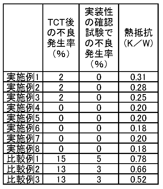
表から分かる通り、実施例にかかるリード端子付きセラミックス回路基板は、TCT特性、実装性共に良好な結果が得られた。それに対し、比較例はうねりが大きいため特性が低下した。このため、実施例は厚いリード端子を接合するセラミックス回路基板に好適であることが分かった。窒化珪素基板を0.32mm以下、さらには0.25mm以下と薄くしても優れた耐久性を示した。
As can be seen from the table, the ceramic circuit board with lead terminals according to the example gave good results in both TCT characteristics and mountability. On the other hand, the characteristics of the comparative example deteriorated due to large waviness. For this reason, it turned out that an Example is suitable for the ceramic circuit board which joins a thick lead terminal. Even when the silicon nitride substrate was thinned to 0.32 mm or less, and further to 0.25 mm or less, excellent durability was exhibited.
以上、本発明のいくつかの実施形態を例示したが、これらの実施形態は、例として提示したものであり、発明の範囲を限定することは意図していない。これら新規な実施形態は、その他の様々な形態で実施されることが可能であり、発明の要旨を逸脱しない範囲で、種々の省略、置き換え、変更などを行うことができる。これら実施形態やその変形例は、発明の範囲や要旨に含まれるとともに、特許請求の範囲に記載された発明とその均等の範囲に含まれる。また、前述の各実施形態は、相互に組み合わせて実施することができる。
As mentioned above, although some embodiment of this invention was illustrated, these embodiment is shown as an example and is not intending limiting the range of invention. These novel embodiments can be implemented in various other forms, and various omissions, replacements, changes, and the like can be made without departing from the spirit of the invention. These embodiments and modifications thereof are included in the scope and gist of the invention, and are included in the invention described in the claims and equivalents thereof. Further, the above-described embodiments can be implemented in combination with each other.
Claims (11)
- 第1の面と第2の面とを有し、前記第1の面が第1の領域と第2の領域とを含む、厚さ1.0mm以下のセラミックス基板と、
前記第1の領域に接合された第1の金属板と、
前記第2の面に接合された第2の金属板と、を具備し、
前記第1の面の第1の辺に沿って測定される前記第2の領域の第1のうねり曲線は、1つ以下の極値を有し、
前記第1の面の第2の辺に沿って測定される前記第2の領域の第2のうねり曲線は、2つ以上3つ以下の極値を有する、セラミックス回路基板。 A ceramic substrate having a thickness of 1.0 mm or less, wherein the ceramic substrate has a first surface and a second surface, and the first surface includes the first region and the second region;
A first metal plate joined to the first region;
A second metal plate joined to the second surface,
The first undulation curve of the second region measured along the first side of the first surface has no more than one extreme value;
The ceramic circuit board, wherein the second waviness curve of the second region measured along the second side of the first surface has two or more and three or less extreme values. - 前記第1のうねり曲線は、略円弧形状であり、
前記第2のうねり曲線は、略M字形状または略S字形状である、請求項1に記載のセラミックス回路基板。 The first undulation curve has a substantially arc shape,
2. The ceramic circuit board according to claim 1, wherein the second undulation curve has a substantially M shape or a substantially S shape. - 前記第1の金属板および前記第2の金属板の少なくとも一つの厚さが0.6mm以上である、請求項1に記載のセラミックス回路基板。 The ceramic circuit board according to claim 1, wherein the thickness of at least one of the first metal plate and the second metal plate is 0.6 mm or more.
- 前記第1の金属板および前記第2の金属板のうち最も厚い金属板の厚さは、前記セラミックス基板の厚さの1.5倍以下である、請求項1に記載のセラミックス回路基板。 The ceramic circuit board according to claim 1, wherein a thickness of the thickest metal plate among the first metal plate and the second metal plate is 1.5 times or less of a thickness of the ceramic substrate.
- 前記第1の辺の長さは、前記第2の辺の長さの1.25倍以上である、請求項1に記載のセラミックス回路基板。 The ceramic circuit board according to claim 1, wherein the length of the first side is 1.25 times or more of the length of the second side.
- 前記セラミックス基板は、厚さ0.33mm以下の窒化珪素基板である、請求項1に記載のセラミックス回路基板。 The ceramic circuit substrate according to claim 1, wherein the ceramic substrate is a silicon nitride substrate having a thickness of 0.33 mm or less.
- 前記第1の金属板および前記第2の金属板の少なくとも一つは、接合層を介して前記セラミックス基板に接合されている、請求項1に記載のセラミックス回路基板。 2. The ceramic circuit board according to claim 1, wherein at least one of the first metal plate and the second metal plate is bonded to the ceramic substrate via a bonding layer.
- 前記第1のうねり曲線および前記第2のうねり曲線の少なくとも一つの最大値と最小値との差が10μm以上である、請求項1に記載のセラミックス回路基板。 2. The ceramic circuit board according to claim 1, wherein a difference between at least one maximum value and minimum value of the first undulation curve and the second undulation curve is 10 μm or more.
- 前記第1の金属板に接合された、厚さ0.2mm以上のリード端子をさらに具備する、請求項1に記載のセラミックス回路基板。 The ceramic circuit board according to claim 1, further comprising a lead terminal having a thickness of 0.2 mm or more joined to the first metal plate.
- 前記第1のうねり曲線および前記第2のうねり曲線の少なくとも一つの最大値と最小値の差が40μm以下である、請求項9に記載のセラミックス回路基板。 10. The ceramic circuit board according to claim 9, wherein a difference between at least one maximum value and minimum value of the first undulation curve and the second undulation curve is 40 μm or less.
- 請求項9に記載のセラミックス回路基板と、
前記第1の金属板の上に設けられた半導体素子と、
前記第2の金属板の上に設けられた放熱部材と、を具備する、半導体モジュール。 A ceramic circuit board according to claim 9;
A semiconductor element provided on the first metal plate;
And a heat dissipating member provided on the second metal plate.
Priority Applications (7)
| Application Number | Priority Date | Filing Date | Title |
|---|---|---|---|
| EP17827739.8A EP3486942A4 (en) | 2016-07-14 | 2017-07-14 | Ceramic circuit board and semiconductor module |
| CN202210831284.3A CN115172290A (en) | 2016-07-14 | 2017-07-14 | Ceramic circuit board and semiconductor module |
| CN201780042696.6A CN109417057B (en) | 2016-07-14 | 2017-07-14 | Ceramic circuit board and semiconductor module |
| JP2018527681A JP7048493B2 (en) | 2016-07-14 | 2017-07-14 | Ceramic circuit boards and semiconductor modules |
| US16/246,106 US10595403B2 (en) | 2016-07-14 | 2019-01-11 | Ceramic circuit board and semiconductor module |
| US16/781,741 US10952317B2 (en) | 2016-07-14 | 2020-02-04 | Ceramic circuit board and semiconductor module |
| JP2022001392A JP7204962B2 (en) | 2016-07-14 | 2022-01-07 | Ceramic circuit boards and semiconductor modules |
Applications Claiming Priority (2)
| Application Number | Priority Date | Filing Date | Title |
|---|---|---|---|
| JP2016139735 | 2016-07-14 | ||
| JP2016-139735 | 2016-07-14 |
Related Child Applications (1)
| Application Number | Title | Priority Date | Filing Date |
|---|---|---|---|
| US16/246,106 Continuation US10595403B2 (en) | 2016-07-14 | 2019-01-11 | Ceramic circuit board and semiconductor module |
Publications (1)
| Publication Number | Publication Date |
|---|---|
| WO2018012616A1 true WO2018012616A1 (en) | 2018-01-18 |
Family
ID=60952132
Family Applications (1)
| Application Number | Title | Priority Date | Filing Date |
|---|---|---|---|
| PCT/JP2017/025729 WO2018012616A1 (en) | 2016-07-14 | 2017-07-14 | Ceramic circuit board and semiconductor module |
Country Status (5)
| Country | Link |
|---|---|
| US (2) | US10595403B2 (en) |
| EP (1) | EP3486942A4 (en) |
| JP (2) | JP7048493B2 (en) |
| CN (2) | CN115172290A (en) |
| WO (1) | WO2018012616A1 (en) |
Cited By (3)
| Publication number | Priority date | Publication date | Assignee | Title |
|---|---|---|---|---|
| WO2019167942A1 (en) * | 2018-02-27 | 2019-09-06 | 三菱マテリアル株式会社 | Insulating circuit board |
| WO2020158775A1 (en) * | 2019-01-30 | 2020-08-06 | デンカ株式会社 | Heat-dissipating member and manufacturing method for same |
| JP2020123714A (en) * | 2019-06-05 | 2020-08-13 | デンカ株式会社 | Heat-dissipating member and manufacturing method thereof |
Citations (3)
| Publication number | Priority date | Publication date | Assignee | Title |
|---|---|---|---|---|
| JP2004134703A (en) * | 2002-10-15 | 2004-04-30 | Toshiba Corp | Circuit board with terminal |
| JP2006019494A (en) * | 2004-07-01 | 2006-01-19 | Hitachi Metals Ltd | Silicon nitride circuit board and semiconductor module |
| WO2015019602A1 (en) * | 2013-08-08 | 2015-02-12 | 株式会社 東芝 | Circuit substrate and semiconductor device |
Family Cites Families (27)
| Publication number | Priority date | Publication date | Assignee | Title |
|---|---|---|---|---|
| DE4233073A1 (en) * | 1992-10-01 | 1994-04-07 | Siemens Ag | Semiconductor modular structure prodn. - by convexly shaping and bonding in single hot pressing operation |
| EP0805492B1 (en) * | 1996-04-03 | 2004-06-30 | Jürgen Dr.-Ing. Schulz-Harder | Curved metal ceramic substrate |
| US5691467A (en) * | 1996-06-28 | 1997-11-25 | International Business Machines Corporation | Method for mapping surfaces adapted for receiving electrical components |
| JP3919398B2 (en) * | 1999-10-27 | 2007-05-23 | 三菱電機株式会社 | Semiconductor module |
| JP3886707B2 (en) * | 2000-08-09 | 2007-02-28 | 京セラ株式会社 | Manufacturing method of ceramic substrate |
| JP5038565B2 (en) * | 2000-09-22 | 2012-10-03 | 株式会社東芝 | Ceramic circuit board and manufacturing method thereof |
| US6613443B2 (en) * | 2000-10-27 | 2003-09-02 | Kabushiki Kaisha Toshiba | Silicon nitride ceramic substrate, silicon nitride ceramic circuit board using the substrate, and method of manufacturing the substrate |
| JP4197447B2 (en) * | 2003-03-31 | 2008-12-17 | 富士フイルム株式会社 | Method for manufacturing organic electroluminescent device and organic electroluminescent device |
| WO2006049086A1 (en) * | 2004-11-01 | 2006-05-11 | Matsushita Electric Industrial Co., Ltd. | Light emitting module, lighting device, and display device |
| JP2006253298A (en) * | 2005-03-09 | 2006-09-21 | Toshiba Corp | Semiconductor light emitting element and device therefor |
| JP4969995B2 (en) * | 2006-08-21 | 2012-07-04 | 株式会社日立製作所 | Solid-state imaging device and manufacturing method thereof |
| JP5016975B2 (en) * | 2007-03-05 | 2012-09-05 | 株式会社東芝 | Manufacturing method of semiconductor device |
| JP5439729B2 (en) * | 2008-03-10 | 2014-03-12 | 日立金属株式会社 | Silicon nitride substrate, manufacturing method thereof, silicon nitride circuit substrate and semiconductor module using the same |
| US8324723B2 (en) * | 2008-03-25 | 2012-12-04 | Bridge Semiconductor Corporation | Semiconductor chip assembly with bump/base heat spreader and dual-angle cavity in bump |
| EP3273755B1 (en) | 2009-09-15 | 2018-11-07 | Kabushiki Kaisha Toshiba | Process for producing a ceramic circuit board |
| JP5588956B2 (en) * | 2011-11-30 | 2014-09-10 | 株式会社 日立パワーデバイス | Power semiconductor device |
| JP2013229579A (en) * | 2012-03-30 | 2013-11-07 | Mitsubishi Materials Corp | Substrate for power module, substrate for power module having heat sink, and power module |
| CN104718615B (en) * | 2012-10-04 | 2018-01-02 | 株式会社东芝 | Semiconductor circuit board and its manufacture method and use its semiconductor device |
| JP6172947B2 (en) | 2013-01-11 | 2017-08-02 | キヤノン株式会社 | Zoom lens and imaging apparatus having the same |
| JP2014207389A (en) * | 2013-04-15 | 2014-10-30 | 株式会社東芝 | Semiconductor package |
| JP6051115B2 (en) * | 2013-06-15 | 2016-12-27 | 京セラ株式会社 | Heat dissipation member, electronic device, and image display device |
| US20140376694A1 (en) * | 2013-06-20 | 2014-12-25 | Kabushiki Kaisha Toshiba | Substrate measurement apparatus and substrate measurement method |
| JP5976623B2 (en) * | 2013-11-18 | 2016-08-23 | ニッタ・ハース株式会社 | Workpiece holding material |
| JP2016063013A (en) * | 2014-09-17 | 2016-04-25 | 株式会社東芝 | Semiconductor device |
| JP6867102B2 (en) * | 2014-10-22 | 2021-04-28 | Jx金属株式会社 | Manufacturing method of copper heat dissipation material, copper foil with carrier, connector, terminal, laminate, shield material, printed wiring board, metal processing member, electronic device, and printed wiring board |
| JP6380131B2 (en) * | 2015-01-28 | 2018-08-29 | 日立金属株式会社 | How to adjust the warping amount of the insulating substrate |
| JP6515047B2 (en) * | 2016-03-11 | 2019-05-15 | 東芝メモリ株式会社 | Semiconductor device and method of manufacturing the same |
-
2017
- 2017-07-14 WO PCT/JP2017/025729 patent/WO2018012616A1/en unknown
- 2017-07-14 EP EP17827739.8A patent/EP3486942A4/en active Pending
- 2017-07-14 CN CN202210831284.3A patent/CN115172290A/en active Pending
- 2017-07-14 CN CN201780042696.6A patent/CN109417057B/en active Active
- 2017-07-14 JP JP2018527681A patent/JP7048493B2/en active Active
-
2019
- 2019-01-11 US US16/246,106 patent/US10595403B2/en active Active
-
2020
- 2020-02-04 US US16/781,741 patent/US10952317B2/en active Active
-
2022
- 2022-01-07 JP JP2022001392A patent/JP7204962B2/en active Active
Patent Citations (3)
| Publication number | Priority date | Publication date | Assignee | Title |
|---|---|---|---|---|
| JP2004134703A (en) * | 2002-10-15 | 2004-04-30 | Toshiba Corp | Circuit board with terminal |
| JP2006019494A (en) * | 2004-07-01 | 2006-01-19 | Hitachi Metals Ltd | Silicon nitride circuit board and semiconductor module |
| WO2015019602A1 (en) * | 2013-08-08 | 2015-02-12 | 株式会社 東芝 | Circuit substrate and semiconductor device |
Cited By (7)
| Publication number | Priority date | Publication date | Assignee | Title |
|---|---|---|---|---|
| WO2019167942A1 (en) * | 2018-02-27 | 2019-09-06 | 三菱マテリアル株式会社 | Insulating circuit board |
| JPWO2019167942A1 (en) * | 2018-02-27 | 2020-04-16 | 三菱マテリアル株式会社 | Isolated circuit board |
| WO2020158775A1 (en) * | 2019-01-30 | 2020-08-06 | デンカ株式会社 | Heat-dissipating member and manufacturing method for same |
| JP2020123639A (en) * | 2019-01-30 | 2020-08-13 | デンカ株式会社 | Heat-dissipating member and manufacturing method thereof |
| CN112997300A (en) * | 2019-01-30 | 2021-06-18 | 电化株式会社 | Heat radiation member and method for manufacturing same |
| JP7116690B2 (en) | 2019-01-30 | 2022-08-10 | デンカ株式会社 | Heat dissipation member and manufacturing method thereof |
| JP2020123714A (en) * | 2019-06-05 | 2020-08-13 | デンカ株式会社 | Heat-dissipating member and manufacturing method thereof |
Also Published As
| Publication number | Publication date |
|---|---|
| JP7204962B2 (en) | 2023-01-16 |
| JPWO2018012616A1 (en) | 2019-04-25 |
| CN109417057A (en) | 2019-03-01 |
| EP3486942A4 (en) | 2020-03-18 |
| US10952317B2 (en) | 2021-03-16 |
| JP7048493B2 (en) | 2022-04-05 |
| EP3486942A1 (en) | 2019-05-22 |
| JP2022046758A (en) | 2022-03-23 |
| US20200178387A1 (en) | 2020-06-04 |
| CN109417057B (en) | 2022-08-02 |
| US10595403B2 (en) | 2020-03-17 |
| US20190150278A1 (en) | 2019-05-16 |
| CN115172290A (en) | 2022-10-11 |
Similar Documents
| Publication | Publication Date | Title |
|---|---|---|
| JP7204962B2 (en) | Ceramic circuit boards and semiconductor modules | |
| US9786577B2 (en) | Power module substrate, heat-sink-attached power-module substrate, and heat-sink-attached power module | |
| JP7000545B2 (en) | Manufacturing method of semiconductor module | |
| US10366938B2 (en) | Silicon nitride circuit board and electronic component module using the same | |
| JP7159395B2 (en) | Circuit boards and semiconductor modules | |
| JP2008091959A (en) | Method of manufacturing semiconductor device | |
| JP7151583B2 (en) | Insulated circuit board with heat sink | |
| US10290602B2 (en) | Semiconductor device and method of making semiconductor device | |
| JP5954374B2 (en) | Insulating substrate, manufacturing method thereof, semiconductor module, and semiconductor device | |
| JP7301732B2 (en) | Ceramic circuit board with screw pad member and semiconductor device using the same | |
| JP2012009787A (en) | Substrate for power module and method of manufacturing the same | |
| CN116830813A (en) | Ceramic circuit board and semiconductor device using the same |
Legal Events
| Date | Code | Title | Description |
|---|---|---|---|
| 121 | Ep: the epo has been informed by wipo that ep was designated in this application |
Ref document number: 17827739 Country of ref document: EP Kind code of ref document: A1 |
|
| ENP | Entry into the national phase |
Ref document number: 2018527681 Country of ref document: JP Kind code of ref document: A |
|
| NENP | Non-entry into the national phase |
Ref country code: DE |
|
| ENP | Entry into the national phase |
Ref document number: 2017827739 Country of ref document: EP Effective date: 20190214 |