WO2018010180A1 - Oscillator - Google Patents

Oscillator Download PDF

Info

Publication number
WO2018010180A1
WO2018010180A1 PCT/CN2016/090223 CN2016090223W WO2018010180A1 WO 2018010180 A1 WO2018010180 A1 WO 2018010180A1 CN 2016090223 W CN2016090223 W CN 2016090223W WO 2018010180 A1 WO2018010180 A1 WO 2018010180A1
Authority
WO
WIPO (PCT)
Prior art keywords
mos transistor
capacitor
unit
oscillator
pole
Prior art date
Application number
PCT/CN2016/090223
Other languages
French (fr)
Chinese (zh)
Inventor
时锴
卢磊
谢磊
Original Assignee
华为技术有限公司
Priority date (The priority date is an assumption and is not a legal conclusion. Google has not performed a legal analysis and makes no representation as to the accuracy of the date listed.)
Filing date
Publication date
Application filed by 华为技术有限公司 filed Critical 华为技术有限公司
Priority to KR1020187035111A priority Critical patent/KR20190004332A/en
Priority to CN201680002584.3A priority patent/CN108141177B/en
Priority to CN202111584503.4A priority patent/CN114430263A/en
Priority to EP16908505.7A priority patent/EP3444945A4/en
Priority to PCT/CN2016/090223 priority patent/WO2018010180A1/en
Publication of WO2018010180A1 publication Critical patent/WO2018010180A1/en
Priority to US16/232,726 priority patent/US10622943B2/en

Links

Images

Classifications

    • HELECTRICITY
    • H03ELECTRONIC CIRCUITRY
    • H03KPULSE TECHNIQUE
    • H03K3/00Circuits for generating electric pulses; Monostable, bistable or multistable circuits
    • H03K3/02Generators characterised by the type of circuit or by the means used for producing pulses
    • H03K3/023Generators characterised by the type of circuit or by the means used for producing pulses by the use of differential amplifiers or comparators, with internal or external positive feedback
    • H03K3/0233Bistable circuits
    • H03K3/02335Bistable circuits provided with means for increasing reliability; for protection; for ensuring a predetermined initial state when the supply voltage has been applied; for storing the actual state when the supply voltage fails
    • HELECTRICITY
    • H03ELECTRONIC CIRCUITRY
    • H03BGENERATION OF OSCILLATIONS, DIRECTLY OR BY FREQUENCY-CHANGING, BY CIRCUITS EMPLOYING ACTIVE ELEMENTS WHICH OPERATE IN A NON-SWITCHING MANNER; GENERATION OF NOISE BY SUCH CIRCUITS
    • H03B5/00Generation of oscillations using amplifier with regenerative feedback from output to input
    • H03B5/08Generation of oscillations using amplifier with regenerative feedback from output to input with frequency-determining element comprising lumped inductance and capacitance
    • H03B5/12Generation of oscillations using amplifier with regenerative feedback from output to input with frequency-determining element comprising lumped inductance and capacitance active element in amplifier being semiconductor device
    • H03B5/1237Generation of oscillations using amplifier with regenerative feedback from output to input with frequency-determining element comprising lumped inductance and capacitance active element in amplifier being semiconductor device comprising means for varying the frequency of the generator
    • H03B5/124Generation of oscillations using amplifier with regenerative feedback from output to input with frequency-determining element comprising lumped inductance and capacitance active element in amplifier being semiconductor device comprising means for varying the frequency of the generator the means comprising a voltage dependent capacitance
    • H03B5/1243Generation of oscillations using amplifier with regenerative feedback from output to input with frequency-determining element comprising lumped inductance and capacitance active element in amplifier being semiconductor device comprising means for varying the frequency of the generator the means comprising a voltage dependent capacitance the means comprising voltage variable capacitance diodes
    • HELECTRICITY
    • H03ELECTRONIC CIRCUITRY
    • H03BGENERATION OF OSCILLATIONS, DIRECTLY OR BY FREQUENCY-CHANGING, BY CIRCUITS EMPLOYING ACTIVE ELEMENTS WHICH OPERATE IN A NON-SWITCHING MANNER; GENERATION OF NOISE BY SUCH CIRCUITS
    • H03B5/00Generation of oscillations using amplifier with regenerative feedback from output to input
    • H03B5/08Generation of oscillations using amplifier with regenerative feedback from output to input with frequency-determining element comprising lumped inductance and capacitance
    • H03B5/12Generation of oscillations using amplifier with regenerative feedback from output to input with frequency-determining element comprising lumped inductance and capacitance active element in amplifier being semiconductor device
    • H03B5/1206Generation of oscillations using amplifier with regenerative feedback from output to input with frequency-determining element comprising lumped inductance and capacitance active element in amplifier being semiconductor device using multiple transistors for amplification
    • H03B5/1212Generation of oscillations using amplifier with regenerative feedback from output to input with frequency-determining element comprising lumped inductance and capacitance active element in amplifier being semiconductor device using multiple transistors for amplification the amplifier comprising a pair of transistors, wherein an output terminal of each being connected to an input terminal of the other, e.g. a cross coupled pair
    • H03B5/1215Generation of oscillations using amplifier with regenerative feedback from output to input with frequency-determining element comprising lumped inductance and capacitance active element in amplifier being semiconductor device using multiple transistors for amplification the amplifier comprising a pair of transistors, wherein an output terminal of each being connected to an input terminal of the other, e.g. a cross coupled pair the current source or degeneration circuit being in common to both transistors of the pair, e.g. a cross-coupled long-tailed pair
    • HELECTRICITY
    • H03ELECTRONIC CIRCUITRY
    • H03BGENERATION OF OSCILLATIONS, DIRECTLY OR BY FREQUENCY-CHANGING, BY CIRCUITS EMPLOYING ACTIVE ELEMENTS WHICH OPERATE IN A NON-SWITCHING MANNER; GENERATION OF NOISE BY SUCH CIRCUITS
    • H03B5/00Generation of oscillations using amplifier with regenerative feedback from output to input
    • H03B5/08Generation of oscillations using amplifier with regenerative feedback from output to input with frequency-determining element comprising lumped inductance and capacitance
    • H03B5/12Generation of oscillations using amplifier with regenerative feedback from output to input with frequency-determining element comprising lumped inductance and capacitance active element in amplifier being semiconductor device
    • H03B5/1228Generation of oscillations using amplifier with regenerative feedback from output to input with frequency-determining element comprising lumped inductance and capacitance active element in amplifier being semiconductor device the amplifier comprising one or more field effect transistors
    • HELECTRICITY
    • H03ELECTRONIC CIRCUITRY
    • H03BGENERATION OF OSCILLATIONS, DIRECTLY OR BY FREQUENCY-CHANGING, BY CIRCUITS EMPLOYING ACTIVE ELEMENTS WHICH OPERATE IN A NON-SWITCHING MANNER; GENERATION OF NOISE BY SUCH CIRCUITS
    • H03B5/00Generation of oscillations using amplifier with regenerative feedback from output to input
    • H03B5/08Generation of oscillations using amplifier with regenerative feedback from output to input with frequency-determining element comprising lumped inductance and capacitance
    • H03B5/12Generation of oscillations using amplifier with regenerative feedback from output to input with frequency-determining element comprising lumped inductance and capacitance active element in amplifier being semiconductor device
    • H03B5/1237Generation of oscillations using amplifier with regenerative feedback from output to input with frequency-determining element comprising lumped inductance and capacitance active element in amplifier being semiconductor device comprising means for varying the frequency of the generator
    • H03B5/1262Generation of oscillations using amplifier with regenerative feedback from output to input with frequency-determining element comprising lumped inductance and capacitance active element in amplifier being semiconductor device comprising means for varying the frequency of the generator the means comprising switched elements
    • H03B5/1265Generation of oscillations using amplifier with regenerative feedback from output to input with frequency-determining element comprising lumped inductance and capacitance active element in amplifier being semiconductor device comprising means for varying the frequency of the generator the means comprising switched elements switched capacitors
    • HELECTRICITY
    • H03ELECTRONIC CIRCUITRY
    • H03BGENERATION OF OSCILLATIONS, DIRECTLY OR BY FREQUENCY-CHANGING, BY CIRCUITS EMPLOYING ACTIVE ELEMENTS WHICH OPERATE IN A NON-SWITCHING MANNER; GENERATION OF NOISE BY SUCH CIRCUITS
    • H03B7/00Generation of oscillations using active element having a negative resistance between two of its electrodes
    • H03B7/02Generation of oscillations using active element having a negative resistance between two of its electrodes with frequency-determining element comprising lumped inductance and capacitance
    • H03B7/06Generation of oscillations using active element having a negative resistance between two of its electrodes with frequency-determining element comprising lumped inductance and capacitance active element being semiconductor device
    • HELECTRICITY
    • H03ELECTRONIC CIRCUITRY
    • H03KPULSE TECHNIQUE
    • H03K3/00Circuits for generating electric pulses; Monostable, bistable or multistable circuits
    • H03K3/01Details
    • H03K3/011Modifications of generator to compensate for variations in physical values, e.g. voltage, temperature
    • HELECTRICITY
    • H03ELECTRONIC CIRCUITRY
    • H03KPULSE TECHNIQUE
    • H03K3/00Circuits for generating electric pulses; Monostable, bistable or multistable circuits
    • H03K3/01Details
    • H03K3/012Modifications of generator to improve response time or to decrease power consumption
    • HELECTRICITY
    • H03ELECTRONIC CIRCUITRY
    • H03KPULSE TECHNIQUE
    • H03K3/00Circuits for generating electric pulses; Monostable, bistable or multistable circuits
    • H03K3/01Details
    • H03K3/013Modifications of generator to prevent operation by noise or interference
    • HELECTRICITY
    • H03ELECTRONIC CIRCUITRY
    • H03LAUTOMATIC CONTROL, STARTING, SYNCHRONISATION, OR STABILISATION OF GENERATORS OF ELECTRONIC OSCILLATIONS OR PULSES
    • H03L7/00Automatic control of frequency or phase; Synchronisation
    • H03L7/06Automatic control of frequency or phase; Synchronisation using a reference signal applied to a frequency- or phase-locked loop
    • H03L7/08Details of the phase-locked loop
    • H03L7/099Details of the phase-locked loop concerning mainly the controlled oscillator of the loop
    • H04B5/24
    • HELECTRICITY
    • H03ELECTRONIC CIRCUITRY
    • H03BGENERATION OF OSCILLATIONS, DIRECTLY OR BY FREQUENCY-CHANGING, BY CIRCUITS EMPLOYING ACTIVE ELEMENTS WHICH OPERATE IN A NON-SWITCHING MANNER; GENERATION OF NOISE BY SUCH CIRCUITS
    • H03B2200/00Indexing scheme relating to details of oscillators covered by H03B
    • H03B2200/0002Types of oscillators
    • H03B2200/0008Colpitts oscillator
    • HELECTRICITY
    • H03ELECTRONIC CIRCUITRY
    • H03BGENERATION OF OSCILLATIONS, DIRECTLY OR BY FREQUENCY-CHANGING, BY CIRCUITS EMPLOYING ACTIVE ELEMENTS WHICH OPERATE IN A NON-SWITCHING MANNER; GENERATION OF NOISE BY SUCH CIRCUITS
    • H03B2200/00Indexing scheme relating to details of oscillators covered by H03B
    • H03B2200/003Circuit elements of oscillators
    • H03B2200/004Circuit elements of oscillators including a variable capacitance, e.g. a varicap, a varactor or a variable capacitance of a diode or transistor
    • HELECTRICITY
    • H03ELECTRONIC CIRCUITRY
    • H03BGENERATION OF OSCILLATIONS, DIRECTLY OR BY FREQUENCY-CHANGING, BY CIRCUITS EMPLOYING ACTIVE ELEMENTS WHICH OPERATE IN A NON-SWITCHING MANNER; GENERATION OF NOISE BY SUCH CIRCUITS
    • H03B2200/00Indexing scheme relating to details of oscillators covered by H03B
    • H03B2200/003Circuit elements of oscillators
    • H03B2200/005Circuit elements of oscillators including measures to switch a capacitor
    • HELECTRICITY
    • H03ELECTRONIC CIRCUITRY
    • H03BGENERATION OF OSCILLATIONS, DIRECTLY OR BY FREQUENCY-CHANGING, BY CIRCUITS EMPLOYING ACTIVE ELEMENTS WHICH OPERATE IN A NON-SWITCHING MANNER; GENERATION OF NOISE BY SUCH CIRCUITS
    • H03B2200/00Indexing scheme relating to details of oscillators covered by H03B
    • H03B2200/003Circuit elements of oscillators
    • H03B2200/0058Circuit elements of oscillators with particular transconductance characteristics, e.g. an operational transconductance amplifier
    • HELECTRICITY
    • H03ELECTRONIC CIRCUITRY
    • H03BGENERATION OF OSCILLATIONS, DIRECTLY OR BY FREQUENCY-CHANGING, BY CIRCUITS EMPLOYING ACTIVE ELEMENTS WHICH OPERATE IN A NON-SWITCHING MANNER; GENERATION OF NOISE BY SUCH CIRCUITS
    • H03B2200/00Indexing scheme relating to details of oscillators covered by H03B
    • H03B2200/006Functional aspects of oscillators
    • H03B2200/0062Bias and operating point
    • HELECTRICITY
    • H03ELECTRONIC CIRCUITRY
    • H03BGENERATION OF OSCILLATIONS, DIRECTLY OR BY FREQUENCY-CHANGING, BY CIRCUITS EMPLOYING ACTIVE ELEMENTS WHICH OPERATE IN A NON-SWITCHING MANNER; GENERATION OF NOISE BY SUCH CIRCUITS
    • H03B2200/00Indexing scheme relating to details of oscillators covered by H03B
    • H03B2200/006Functional aspects of oscillators
    • H03B2200/0088Reduction of noise
    • H03B2200/009Reduction of phase noise
    • HELECTRICITY
    • H04ELECTRIC COMMUNICATION TECHNIQUE
    • H04WWIRELESS COMMUNICATION NETWORKS
    • H04W88/00Devices specially adapted for wireless communication networks, e.g. terminals, base stations or access point devices
    • H04W88/08Access point devices

Definitions

  • Embodiments of the present invention relate to the field of electronic technologies, and in particular, to an oscillator.
  • the oscillator has a wide range of applications.
  • the power consumption and phase noise of the oscillator are the main parameters for measuring the performance of the oscillator, so oscillators with low power consumption and low phase noise have been the subject of long-term research.
  • the oscillator includes a resonant unit 10 and a cross-complementary active connected to the resonant unit 10.
  • Unit 11 the resonance unit 10 is for generating an oscillation signal having a certain oscillation frequency; the cross-complementary active unit 11 is for compensating for the energy consumption of the resonance unit 10, so that the resonance unit 10 outputs a stable oscillation signal.
  • phase noise calculation formula of the oscillator is:
  • represents the frequency offset of the carrier processed or generated by the oscillator
  • q max represents the maximum amount of charge of the current noise source.
  • ⁇ ( ⁇ t) is ISF (Impulse Sensitivity Function), ⁇ ( ⁇ t) is NMF (Noise-modulating Function) whose phase changes with time.
  • ISF describes that at some point in time, at some point The degree of shift in the phase of the output signal caused by the injection of a unit pulse current on each node. Since the waveform of the oscillating signal generated by the Cross-coupled negative-resistance oscillator shown in FIG. 1a is a sine wave, the unit pulse current is injected into the Cross-coupled negative-resistance oscillator at different time points, and then simulation is performed.
  • Figure 1b shows the ISF eff of the Cross-coupled negative-resistance oscillator (ie, ⁇ eff ( ⁇ t) in equation (2)). It can be seen from Fig. 1b that the value of ISF eff is only ⁇ /2 time period (ie 3 ⁇ /2 to 2 ⁇ ) in one oscillation period (2 ⁇ ) is 0, and the remaining 3 ⁇ /2 time period (ie 0 to 3 ⁇ /2) None are 0. Therefore, combining equations (1) and (2), the phase noise of the Cross-coupled negative-resistance oscillator is relatively large in one oscillation period. Therefore, the phase noise performance of the Cross-coupled negative-resistance oscillator is relatively poor.
  • Embodiments of the present invention provide an oscillator capable of achieving performance requirements of low power consumption.
  • an embodiment of the present invention provides a low power consumption low phase noise oscillator, including: a resonant unit, a cross-coupled current source unit, and a positive feedback unit coupled between the current source unit and the resonant unit; a resonant unit for generating a differential oscillating signal having a first oscillating frequency; the positive feedback unit for receiving the differential oscillating signal, and performing gain enhancement on the differential oscillating signal to obtain a differential output oscillating signal; and a current source unit for An adjustable bias current is provided for the resonant unit and the positive feedback unit described above.
  • Embodiments of the present invention provide an oscillator, wherein a current source unit can provide a tunable bias current for a positive feedback unit and a resonance unit, and a Gm-boosted structure with a positive feedback unit, so that the positive feedback unit can
  • the gain enhancement is performed on the received differential oscillating signal to obtain a differential output oscillating signal. Therefore, the power consumption of the oscillator provided by the embodiment of the present invention can be reduced by reducing the bias current under the condition that the oscillator is normally started.
  • the foregoing resonating unit is further configured to output a differential oscillating signal to the current source unit via a positive feedback unit; the current source unit is further configured to be used according to the resonating unit
  • the differential oscillating signal is output, and the bias current is adjusted by controlling the magnitude of the bias voltage to adjust the amplitude of the differential output oscillating signal.
  • the foregoing positive feedback unit includes: a first MOS (metal oxide semiconductor, Metal-Oxide- a transistor, a second MOS transistor, a first capacitor, a second capacitor, a third capacitor, and a fourth capacitor; wherein the first pole of the first MOS transistor As a first output node, respectively connected to the resonant unit and one end of the first capacitor, the second pole of the first MOS transistor is respectively connected to the other end of the first capacitor and one end of the third capacitor, the gate of the first MOS transistor and the first The gates of the two MOS transistors are connected to the first constant voltage source, and the first poles of the second MOS transistors are respectively connected as the second output node to one ends of the resonant unit and the second capacitor, and the second poles of the second MOS transistors are respectively The other end of the second capacitor is connected to one end of the fourth capacitor, the other end of the fourth capacitor is connected
  • a forward differential signal output end is disposed between one end of the three capacitor and the third output node of the current source unit, and a negative differential signal output end is disposed between one end of the fourth capacitor and the fourth output node of the current source unit . This can reduce the effect of the output load on the forward differential oscillating signal and the negative differential oscillating signal.
  • the first constant voltage source is a first power source.
  • the resonating unit includes: a first inductor, a second An inductor and a switched capacitor array; wherein one end of the first inductor is connected to one end of the second inductor, and the other end of the first inductor is respectively connected to one end of the switched capacitor array and the first output node of the positive feedback unit; One end is respectively connected to the other end of the switched capacitor array and the second output node of the positive feedback unit, and one end of the first inductor and one end of the second inductor are connected to the first constant voltage node.
  • the frequency value of the oscillator can be changed by opening or closing the switch in the array of capacitive switches.
  • the current source unit includes: a third MOS transistor, a fourth MOS transistor, a fifth capacitor, and a sixth capacitor a first resistor and a second resistor; wherein a gate of the third MOS transistor is respectively connected to one end of the sixth capacitor and one end of the first resistor, and the drain of the third MOS transistor serves as a third output node and a fifth capacitor respectively One end is connected to one end of the third capacitor; the gate of the fourth MOS transistor is respectively connected to the other end of the fifth capacitor and one end of the second resistor, and the drain of the fourth MOS transistor serves as a fourth output node and a sixth capacitor respectively The other end of the fourth capacitor is connected to one end of the fourth capacitor; the other end of the first resistor and the other end of the second resistor are connected to an adjustable power supply for providing an adjustable bias voltage, current for the current source unit Source unit Specifically, the tunable bias current is provided to the resonant
  • the third MOS transistor and the fourth MOS transistor in the oscillator are adjusted to different working modes, which can effectively reduce the first MOS transistor, the second MOS transistor, and the third in the oscillator.
  • the MOS transistor and the fourth MOS transistor are turned on, when the startup gain in the oscillator is constant, since the on-times of the first MOS transistor, the second MOS transistor, the third MOS transistor, and the fourth MOS transistor become smaller, The current value in one oscillation period is reduced, and since the power consumption is proportional to the current, the power consumption of the oscillator is reduced.
  • the third MOS transistor and the fourth MOS transistor are In the NMOS transistor, the first pole of the first MOS transistor and the first pole of the second MOS transistor are both drains, and the second pole of the first MOS transistor and the second pole of the second MOS transistor are both sources;
  • the first constant voltage node is the first power source and the second constant voltage node is the ground.
  • a seventh possible implementation manner of the first aspect when the first MOS transistor and the second MOS transistor are a PMOS transistor, a third MOS transistor, and a fourth MOS transistor
  • the first pole of the first MOS transistor and the first pole of the second MOS transistor are both drains, and the second pole of the first MOS transistor and the second pole of the second MOS transistor are both sources
  • the first constant voltage node is ground and the second constant voltage node is the first power source.
  • the third MOS transistor and the fourth MOS transistor are In the NMOS transistor, the first pole of the first MOS transistor and the first pole of the second MOS transistor are both sources, and the second pole of the first MOS transistor and the second pole of the second MOS transistor are both drains;
  • the constant voltage node is the first power source and the second constant voltage node is the ground.
  • the first MOS transistor and the second MOS transistor are an NMOS transistor, a third MOS transistor, and a fourth
  • the MOS transistor is a PMOS transistor
  • the first pole of the first MOS transistor and the first pole of the second MOS transistor are both a source, a second pole of the first MOS transistor and a second pole of the second MOS transistor All are drains; the first constant voltage node is ground, and the second constant voltage node is a first power source.
  • the switched capacitor The array includes at least one capacitive switch branch; any of the capacitive switch branches includes a seventh capacitor, a switch, and an eighth capacitor, wherein one end of the seventh capacitor is connected to the other end of the first inductor and the first output node of the positive feedback unit, The other end of the eighth capacitor is connected to the second output node of the positive feedback unit and the other end of the second inductor.
  • the seventh capacitor and the eighth capacitor are adjustable capacitors.
  • the embodiment of the present invention provides a terminal, where the terminal includes at least the short-distance communication device and the oscillation described in any one of the possible implementation manners of the first aspect to the eleventh possible implementation manner of the first aspect.
  • the oscillator is used to provide a local carrier signal for the short-range communication device described above.
  • an embodiment of the present invention provides a base station, where the base station includes at least a transceiver and a phase-locked loop circuit, and the first aspect of the phase-locked loop circuit is any one of the eleventh possible implementation manners of the first aspect.
  • a possible implementation is the oscillator described to provide a local carrier signal for the transceiver described above.
  • 1a is a schematic structural diagram of a Cross-coupled negative resistance oscillator provided in the prior art
  • 1b is a graph showing a simulated ISF function of a Cross-coupled negative-resistance oscillator provided in the prior art
  • FIG. 2 is a schematic structural diagram 1 of an oscillator according to an embodiment of the present invention.
  • FIG. 3 is a schematic structural diagram 2 of an oscillator according to an embodiment of the present invention.
  • 4a is a schematic structural diagram 3 of an oscillator according to an embodiment of the present invention.
  • 4b is a current waveform diagram of a MOS transistor in a Cross-coupled negative-resistance oscillator provided by the prior art
  • 4c is a current waveform diagram of a MOS transistor in an oscillator according to an embodiment of the present invention.
  • FIG. 5 is a schematic structural diagram 4 of an oscillator according to an embodiment of the present disclosure.
  • FIG. 6 is a schematic structural diagram 5 of an oscillator according to an embodiment of the present disclosure.
  • FIG. 7 is a schematic structural diagram 6 of an oscillator according to an embodiment of the present disclosure.
  • FIG. 8 is a schematic structural diagram 7 of an oscillator according to an embodiment of the present disclosure.
  • FIG. 9 is a schematic structural diagram 10 of an oscillator according to an embodiment of the present disclosure.
  • FIG. 10 is a schematic structural diagram 11 of an oscillator according to an embodiment of the present invention.
  • FIG. 11 is a graph showing a simulated ISF function of an oscillator according to an embodiment of the present invention.
  • Each of the MOS tubes in any embodiment or the accompanying drawings may be a single MOS tube that satisfies the required starting gain or the required on-current.
  • the MOS tube combination that needs to meet the required starting gain or the required on-current according to the parallel combination of the plurality of MOS tubes, that is, the sum of the starting gains of each of the plurality of MOS tubes is greater than or equal to
  • Each of the capacitors in the embodiment of the present invention may be a capacitor that satisfies a required capacitance value, or a capacitor combination that is composed of a plurality of capacitors in parallel or in series to satisfy a required capacitance value, that is, The plurality of capacitors are connected in series or in parallel, and the corresponding capacitor value is equal to the required capacitor value.
  • Each inductor in the embodiment of the present invention may be an inductor that satisfies the required inductor value, or may be connected by multiple inductors in series or in
  • an embodiment of the present invention provides an oscillator including a resonating unit 10, a cross-coupled current source unit 30, and a positive feedback unit 20 coupled between the current source unit 30 and the resonating unit 10;
  • the resonant unit 10 is configured to generate a first oscillation frequency
  • the differential oscillating signal 20 is configured to receive the differential oscillating signal and perform gain enhancement on the differential oscillating signal to obtain a differential output oscillating signal;
  • the current source unit 30 is configured to provide an adjustable tunable unit 10 and the positive feedback unit 20 Bias current.
  • a differential oscillation signal output terminal ie, a forward differential oscillation signal output terminal OUTP and a negative differential oscillation signal output terminal OUTN shown in FIG.
  • the current source unit 30 provides the tunable bias current to the resonant unit 10 through the positive feedback unit 20.
  • the embodiment of the invention provides an oscillator, wherein the current source unit can provide a tunable bias current for the positive feedback unit and the resonance unit, and form a Gm-boosted structure with the positive feedback unit, so that the positive feedback unit can
  • the gain enhancement is performed on the received differential oscillating signal to obtain a differential output oscillating signal. Therefore, the power consumption of the oscillator provided by the embodiment of the present invention can be reduced by reducing the bias current under the condition that the oscillator is normally started.
  • the resonant unit 10 is further configured to output the differential oscillating signal to the current source unit 30 via the positive feedback unit 20; the current source unit 30 is further configured to control the bias according to the differential oscillating signal output by the resonant unit 10.
  • the magnitude of the voltage adjusts the bias current to adjust the amplitude of the differential output oscillating signal.
  • the amplitude of the differential oscillating signal output by the resonant unit 10 in the oscillator is equal to the bias current provided by the current source unit 30 in the oscillator for the resonant unit 10 and the positive feedback unit 20 and the resistance in the oscillator (ie, the oscillator)
  • the product of the equivalent impedance of all devices, and the value of the resistor in the oscillator is almost constant, so the amplitude of the differential oscillating signal is proportional to the bias current provided by the current source unit, and because of the bias current
  • the size is proportional to the magnitude of the bias voltage, and thus embodiments of the present invention can vary the magnitude of the bias current in the oscillator by adjusting the magnitude of the bias voltage.
  • the bias voltage can be reduced to reduce the bias current, thereby reducing the oscillator output.
  • the amplitude of the differential oscillating signal if the amplitude of the differential oscillating signal output by the oscillator is too small, the bias voltage can be controlled to be large, and the bias current is increased to increase the amplitude of the differential oscillating signal output by the oscillator, and finally the oscillation Differential oscillation signal The magnitude of the number is stable.
  • the positive feedback unit 20 includes: a first metal oxide semiconductor MOS transistor M1, a second MOS transistor M2, a first capacitor C1, a second capacitor C2, a third capacitor C3, and a first a fourth capacitor C4; wherein the first pole 101 of the first MOS transistor M1 is connected as a first output node to the first end of the resonant unit 10 and one end of the first capacitor C1, respectively, and the second pole 102 of the first MOS transistor M1 is respectively Connected to the other end of the first capacitor C1 and one end of the third capacitor C3, the gate of the first MOS transistor M1 and the gate of the second MOS transistor M2 are both connected to the first constant voltage source 103, and the second MOS transistor M2
  • the first pole 201 is connected to the second end of the resonant unit 10 and one end of the second capacitor C2 as a second output node
  • the second pole 202 of the second MOS transistor M2 is respectively connected to the other end of the second capacitor
  • One end of the C4 is connected, the other end of the fourth capacitor C4 is connected to the other end of the third capacitor C3, and one end of the third capacitor C3 and one end of the fourth capacitor C4 are connected to the current source unit 30 at one end of the third capacitor C3.
  • a forward differential signal output terminal OUTP is disposed between the third output node of the current source unit 30,
  • a negative differential signal output terminal OUTN is provided between one end of the fourth capacitor C4 and the fourth output node of the current source unit 30.
  • the first MOS transistor M1 and the second MOS transistor M2 in the positive feedback unit 20 provide a startup gain when the oscillator oscillates, and pass through the first capacitor C1, the first MOS transistor M1 and the third capacitor C3,
  • the second capacitor C2, the second MOS transistor M2 and the fourth capacitor C4 form an alternating current positive feedback, and the device noise in the oscillator is amplified, so that the oscillator maintains an oscillating state, and passes through the forward differential signal output terminal OUTP and the negative direction.
  • the differential signal output terminal OUTN outputs a differential output oscillation signal.
  • the gates of the first MOS transistor M1 and the second MOS transistor M2 are connected to the first constant voltage source 103, and the first pole 101 and the second pole 102 of the first MOS transistor M1 are respectively connected to one end of the first capacitor C1.
  • the first pole 201 and the second pole 202 of the second MOS transistor are respectively connected to one end and the other end of the second capacitor C2, so that only when the voltage of the differential output oscillating signal is smaller than the voltage of the first constant voltage source 103
  • the ON time of the first MOS transistor M1 and the second MOS transistor M2 in one oscillation period is shortened, that is, the current source unit 30 and the positive during one oscillation period.
  • the time during which the feedback unit 20 injects current noise into the resonance unit 10 becomes shorter, so that the phase noise (converted from current noise) in the oscillator is lower in one oscillation period than in the prior art.
  • the first constant voltage source 103 may be a first power source or other constant voltage source.
  • the embodiment of the present invention does not limit this, and may be selected as needed.
  • the oscillator provided by the embodiment of the present invention has a phase shift characteristic of the first capacitor C1 and the second capacitor C2 such that a waveform of a voltage of the differential oscillation signal and a waveform of the current have a phase shift characteristic of 90 degrees.
  • ⁇ ( ⁇ t) is the NMF whose phase changes with time, and the value of ISF eff can be reduced in one oscillation period, thereby further reducing the phase noise of the oscillator provided by the embodiment of the present invention.
  • the current source unit 30 can provide the tunable bias current for the positive feedback unit 20 and the resonance unit 10, and form a Gm-boosted structure with the positive feedback unit 20, the oscillator can be guaranteed to be normal. Under the condition of startup, the power consumption of the oscillator provided by the embodiment of the present invention can be reduced by reducing the bias current.
  • the current source unit 30 in the embodiment of the present invention includes: a third MOS transistor M3, a fourth MOS transistor M4, a fifth capacitor C5, a sixth capacitor C6, and a first a resistor R1 and a second resistor R2; wherein a gate of the third MOS transistor M3 is respectively connected to one end of the sixth capacitor C6 and one end of the first resistor R1, and the drain of the third MOS transistor M3 serves as a third output node respectively One end of the fifth capacitor C5 and one end of the third capacitor C3 are connected; the gate of the fourth MOS transistor M4 is respectively connected to the other end of the fifth capacitor C5 and one end of the second resistor R2, and the drain of the fourth MOS transistor M4 As the fourth output node, respectively connected to the other end of the sixth capacitor C6 and one end of the fourth capacitor C4; the other end of the first resistor R1 and the other end of the second resistor R2 are connected to the adjustable power source V
  • the current source unit 30 is specifically configured to provide the tunable bias current for the resonant unit 10 and the positive feedback unit 20 through the adjustable power supply Vb; the third MOS transistor M3 The source and the source of the fourth MOS transistor M4 are connected to the second constant voltage node 104.
  • the third MOS transistor M3 and the fourth MOS transistor M4 are PMOS transistors.
  • the current source unit 30 operates similarly to a Colpitts oscillator.
  • the third MOS transistor M3 and the fourth MOS transistor M4 are NMOS (Negative Channel Metal Oxide Semiconductor) tubes
  • the source of the third MOS transistor and the fourth MOS transistor The sources are all grounded.
  • the first MOS transistor M1 and the second MOS transistor M2 may be an NMOS transistor or a PMOS transistor.
  • the third MOS transistor M3 and the fourth MOS transistor M4 are PMOS (Positive Channel Metal Oxide Semiconductor) tubes
  • the source of the third MOS transistor and the fourth MOS The source of the tube is connected to the first power source.
  • the first MOS transistor M1 and the second MOS transistor M2 may be a PMOS transistor or an NMOS transistor.
  • the oscillator provided by the embodiment of the present invention includes four MOS transistors, namely, a first MOS transistor M1, a second MOS transistor M2, a third MOS transistor M3, and a fourth MOS transistor M4.
  • the MOS transistors together form a Gm-boosted structure.
  • the power consumption can be higher under the same conditions, and on the other hand, the same startup gain can be obtained.
  • Power consumption while the prior art (such as the Cross-coupled negative-resistance oscillator shown in Figure 1a) has only two MOS transistors, M1 and M2 as shown in Figure 1a, as shown in Figure 4a and Figure 1a.
  • the Cross-coupled negative-resistance oscillator shown in FIG. 1a needs to consume more current to satisfy the above-mentioned startup gain. Since the power consumption of the oscillator is proportional to the current, the present invention The power consumption of implementing an oscillator such as that shown in Figure 4a is lower than in the prior art.
  • the fifth capacitor C5 and the sixth capacitor C6 mainly function to output the gate DC voltage of the third MOS transistor M3 and the fourth MOS transistor M4 and the positive feedback unit 20.
  • the DC voltage is isolated to prevent the DC voltage output from the positive feedback unit 20 from affecting the third MOS transistor M3 and the fourth MOS transistor M4.
  • the third MOS transistor M3 and the fourth MOS transistor M4 can be adjusted to different operating modes by controlling the voltage magnitude of the output of the adjustable power supply Vb, for example, The operating modes of the three MOS transistors M3 and the fourth MOS transistor M4 are adjusted from the current operating mode to the first operating mode such that the current source unit 30 provides the tunable bias current for the resonant unit 10 and the positive feedback unit 20.
  • the first working mode includes, but is not limited to, a class A working mode (also referred to as a class A working mode) and a class B (class B) working mode (also referred to as a class B working mode).
  • Class C (Class C) working mode also known as Class C working mode
  • D Class (Class D) working mode also known as D-class working mode
  • Class E (Class E) working mode in addition to the above five working modes, the first working mode may be another working mode that satisfies the use requirement, for example, a Class AB working mode (also referred to as A and B). Class working mode).
  • the first working mode in the embodiment of the present invention is a class A working mode
  • the third MOS transistor M3 and the fourth MOS transistor M4 in the current source unit 30 operate in the class A working mode, in one During the oscillation period, the third MOS transistor M3 and the fourth MOS transistor M4 in the current source unit 30 are both turned on, but since the gate of the first MOS transistor is connected to the first constant voltage source 103, the gate of the second MOS transistor is connected.
  • the first constant voltage source being an adjustable power supply, only when the absolute value of the gate-source voltage difference between the first MOS transistor M1 and the second MOS transistor M2 is greater than the first MOS transistor M1 and the second MOS transistor
  • the threshold voltage of M2 that is, the absolute value of the turn-on voltage UGS(th)
  • the first MOS transistor M1 and the second MOS transistor M2 are turned on, that is, the amplitude of the forward differential output oscillating signal output by the positive feedback unit.
  • the first MOS transistor M1 and the second MOS transistor M2 are turned on, In the embodiment of the invention, therefore, when both the third MOS transistor M3 and the fourth MOS transistor M4 are turned on in one oscillation period, the first MOS transistor M1
  • the working state of the second MOS transistor M2 is in the C-type working mode or the working mode deeper than the C-type working mode (for example, the D-type working mode, the E-type working mode).
  • the first working mode in the embodiment of the present invention is a class B working mode, that is, the third MOS transistor M3 and the fourth MOS transistor M4 in the current source unit 30 operate in the class B working mode, before an oscillation period.
  • the third MOS transistor M3 is turned on, and since the source of the second MOS transistor is connected to the gate of the third MOS transistor, when the absolute value of the gate-source voltage difference of the second MOS transistor M2 is greater than the second
  • the MOS transistor M2 has a threshold voltage
  • the second MOS transistor M2 is turned on, and when the absolute value of the gate-source voltage difference of the second MOS transistor M2 is smaller than the threshold voltage of the second MOS transistor M2, the second MOS transistor M2 is turned off;
  • the fourth MOS transistor M4 is turned off, the first MOS transistor M1 is turned off; in the second 1/2 period of the oscillation period, the third MOS transistor M3 is turned off, the second MOS transistor M2 is turned off; the fourth MOS transistor M4 is turned on
  • the fourth MOS transistor M4 is turned on during the first 1/2 period of an oscillation period.
  • the first MOS transistor M1 is turned on.
  • the third MOS transistor M3 is turned off, and the second MOS transistor M2 is turned off.
  • the fourth MOS transistor M4 is turned off, the first MOS transistor M1 is turned off, and the third MOS transistor M3 is turned on.
  • the second MOS transistor M2 is turned on.
  • the first working mode in the embodiment of the present invention is the C-type working mode
  • the third MOS transistor M3 and the fourth MOS transistor M4 in the current source unit 30 operate in the C-type working mode, before one oscillation period In the 1/3 period, the third MOS transistor M3 is turned on, and since the source of the second MOS transistor M2 is connected to the gate of the third MOS transistor M3, when the absolute value of the gate-source voltage difference of the second MOS transistor is greater than When the threshold voltage of the second MOS transistor M2 is reached, the second MOS transistor M2 is turned on, and the fourth MOS transistor M4 is turned off.
  • the first MOS transistor M1 Since the source of the first MOS transistor M1 is connected to the gate of the fourth MOS transistor M4, the first MOS transistor M1 is turned off; in the second 2/3 cycle of the oscillation period, the third MOS transistor M3 is turned off, and since the source of the second MOS transistor M2 is connected to the gate of the third MOS transistor M3, when the third MOS transistor M3 When the second MOS is turned off, the fourth MOS transistor M4 is turned on, and since the source of the second MOS transistor is connected to the gate of the fourth MOS transistor, when the absolute value of the gate-source voltage difference of the first MOS transistor M1 is greater than When the threshold voltage of the first MOS transistor M1 is reached, the first MOS transistor M1 is turned on.
  • the fourth MOS transistor M4 is turned on, and when the absolute value of the gate-source voltage difference of the first MOS transistor M1 is greater than the threshold voltage of the first MOS transistor M1, the first MOS The tube M1 is turned on; the third MOS transistor M3 is turned off, and the second MOS transistor M2 is turned off; in the second 2/3 period of the oscillation period, the fourth MOS transistor M4 is turned off, the first MOS transistor M1 is turned off, and the third MOS transistor M3 is turned off. Turning on, when the absolute value of the gate-source voltage difference of the second MOS transistor M2 is greater than the threshold voltage, the second MOS transistor M2 is turned on.
  • the first working mode in the embodiment of the present invention is the D-type working mode
  • the third MOS transistor M3 and the fourth MOS transistor M4 in the current source unit 30 operate in the D-type working mode, before an oscillation period In the 1/4 cycle
  • the fourth MOS transistor M4 is turned off, the first MOS transistor is turned off, and the third MOS transistor M3 is turned on.
  • the second MOS transistor M2 is on; 3/4 weeks after the oscillation period During the period, the third MOS transistor M3 is turned off, the second MOS transistor M2 is turned off, and the fourth MOS transistor M4 is turned on.
  • the first MOS transistor M1 When the absolute value of the gate-source voltage difference of the first MOS transistor M1 is greater than the threshold voltage of the first MOS transistor M1, The first MOS transistor M1 is turned on. Or in the first quarter cycle of an oscillation period, the third MOS transistor M3 is turned off, the second MOS transistor M2 is turned off, and the fourth MOS transistor M4 is turned on, when the gate-source voltage of the first MOS transistor M1 is larger than the first MOS transistor When the threshold voltage of M1 is reached, the first MOS transistor M1 is turned on; in the last 3/4 period of the oscillation period, the fourth MOS transistor M4 is turned off, the first MOS transistor M1 is turned off, and the third MOS transistor M3 is turned on. When the absolute value of the gate-source voltage difference of the second MOS transistor M2 is greater than the threshold voltage of the second MOS transistor M2, the second MOS transistor M2 is turned on.
  • the first working mode in the embodiment of the present invention is the E-type working mode
  • the third MOS transistor M3 and the fourth MOS transistor M4 in the current source unit 30 operate in the E-type working mode, before an oscillation period In the 1/5 cycle, the fourth MOS transistor M4 is turned off, the first MOS transistor M1 is turned off, and the third MOS transistor M3 is turned on.
  • the second MOS transistor M2 When the absolute value of the gate-source voltage difference of the second MOS transistor M2 is greater than the threshold of the second MOS transistor M2 When the voltage is applied, the second MOS transistor M2 is turned on; during the last 4/5 cycles of the oscillation period, the third MOS transistor M3 is turned off, the second MOS transistor M1 is turned off, and the fourth MOS transistor M4 is turned on, when the first MOS transistor is turned on.
  • the absolute value of the gate-source voltage difference of M1 is larger than the threshold voltage of the first MOS transistor M1, the first MOS transistor M1 is turned on.
  • the third MOS transistor M3 is turned off, the second MOS transistor M2 is turned off, and the fourth MOS transistor M4 is turned on, when the absolute value of the gate-source voltage difference of the first MOS transistor M1 is greater than When the threshold voltage of the first MOS transistor M1 is reached, the first MOS transistor M1 is turned on; during the last 4/5 cycles of the oscillation period, the fourth MOS transistor M4 is turned off, the first MOS transistor M1 is turned off, and the third MOS transistor M3 is turned on.
  • the second MOS transistor M2 is turned on.
  • the first working mode in the embodiment of the present invention is the above-described work of the class A working mode, the class B working mode, the class C working mode, the class D working mode, and the class E working mode
  • the fourth MOS transistor M4 is turned off, the first MOS transistor M1 is turned off, and the third MOS transistor M3 is turned on, when the gate of the second MOS transistor M2 is turned on.
  • the second MOS transistor M2 When the absolute value of the source voltage difference is greater than the threshold voltage of the second MOS transistor M2, the second MOS transistor M2 is turned on; after the oscillation period (M-1) /M cycles, the third MOS transistor M3 is turned off, the second MOS transistor M2 is turned off, and the fourth MOS transistor M4 is turned on, when the absolute value of the gate-source voltage difference of the first MOS transistor M1 is greater than the threshold voltage of the first MOS transistor M1 At the time, the first MOS transistor M1 is turned on.
  • the third MOS transistor M3 is turned off, the second MOS transistor M2 is turned off, and the fourth MOS transistor M4 is turned on, when the absolute value of the gate-source voltage difference of the first MOS transistor M1 is greater than When the threshold voltage of the first MOS transistor M1 is reached, the first MOS transistor M1 is turned on; after (M-1)/M cycles of the oscillation period, the fourth MOS transistor M4 is turned off, and the first MOS transistor M1 is turned off, and the third The MOS transistor M3 is turned on, and when the absolute value of the gate-source voltage difference of the second MOS transistor M2 is greater than the threshold voltage of the second MOS transistor M2, the second MOS transistor M2 is turned on.
  • the first MOS tube M1 and the second MOS tube in the positive feedback unit 20 need to have a higher cross.
  • the first MOS transistor M1 and the second MOS transistor M2 need to consume more current, so that the power consumption of the oscillator is relatively large.
  • the working modes of the third MOS transistor and the fourth MOS transistor may be set to the C-type working mode or ratio by adjusting the magnitude of the bias voltage Vb.
  • the C mode of operation has a deeper working mode (ie, the conduction time of the third MOS transistor and the fourth MOS transistor is smaller than the conduction time of the third MOS transistor and the fourth MOS transistor in the C mode of operation), so that the current source unit
  • the positive feedback unit 20 and the resonant unit 10 in the oscillator provided by the embodiment of the present invention provide a bias current and a starting gain.
  • the first MOS transistor M1 and the second MOS transistor M2 in the positive feedback unit 20 provide a startup gain when the oscillator oscillates, and pass through the first capacitor C1, the first MOS transistor M1 and the third capacitor C3,
  • the second capacitor C2, the second MOS transistor M2 and the fourth capacitor C4 form an alternating current positive feedback, the device noise in the oscillator is amplified, so that the oscillator maintains an oscillating state to output a differential oscillating signal; and because the first MOS transistor And a second constant voltage source connected to the gate of the second MOS transistor, and the first pole 101 and the second of the first MOS transistor M1
  • the poles 102 are respectively connected to one end and the other end of the first capacitor C1, and the first pole 201 and the second pole 202 of the second MOS transistor M2 are respectively connected to one end and the other end of the second capacitor C2, and therefore, only when the forward difference is The absolute value of the voltage of the oscillating signal and the gate-source voltage difference of the first
  • the oscillator provided by the embodiment of the present invention has a phase shift characteristic of the first capacitor C1 and the second capacitor C2 such that a waveform of a voltage of the differential oscillation signal and a waveform of the current have a phase shift characteristic of 90 degrees, thereby
  • FIG. 4b is a current waveform diagram of a Cross-coupled negative-resistance oscillator provided in the prior art
  • FIG. 4c is a third MOS transistor and a fourth MOS according to an embodiment of the present invention.
  • the broken line represents the current waveform of the MOS transistor M102 in the prior art Cross-coupled negative-resistance oscillator
  • the solid line represents the current waveform of the MOS transistor M101 in the prior art Cross-coupled negative-resistance oscillator.
  • FIG. 4b is a current waveform diagram of a Cross-coupled negative-resistance oscillator provided in the prior art
  • FIG. 4c is a third MOS transistor and a fourth MOS according to an embodiment of the present invention.
  • the broken line represents the current waveform of the MOS transistor M102 in the prior art Cross-coupled negative-
  • the broken line represents the current waveform diagram of the bias current when the operation mode of the fourth MOS transistor M4 is the C-type operation mode
  • the solid line represents the bias mode when the operation mode of the third MOS transistor M3 is the C-type operation mode.
  • Current waveform of the current As can be seen from FIG. 4c, in the first 1/3 cycle of one oscillation period, the third MOS transistor M3 is turned on, and the fourth MOS transistor M4 is turned off, and the third MOS transistor M3 is in the second 2/3 cycle of one oscillation period. At the end, the fourth MOS transistor M4 is turned on, but the current waveform diagram of the Cross coupled negative resistance oscillator shown in FIG. 4b is before an oscillation period.
  • the MOS transistor M101 in the cross-complementary active cell is turned on, and the MOS transistor M102 is turned off.
  • the MOS transistor M101 is turned off, and the MOS transistor M102 is turned on. Therefore, the present invention is implemented.
  • the active devices in the oscillator provided by the example for example, the third MOS transistor, the fourth MOS transistor, and the first MOS transistor and the second MOS transistor) have a short on-time and a small RMS current in one oscillation period, which saves The advantages of power consumption.
  • the bias voltage Vb may be less than or equal to the voltage of the first power source VCC.
  • the resonant unit 10 includes: a first inductor L1, a second inductor L2, and a switched capacitor array; wherein, one end and the second of the first inductor L1 One end of the inductor L2 is connected, and the other end of the first inductor L1 is respectively connected to one end of the switched capacitor array and the first output node of the positive feedback unit 20; the other end of the second inductor L2 is respectively connected to the other end of the switched capacitor array and positive feedback
  • the second output node of the unit 20 is connected, and one end of the first inductor L1 and one end of the second inductor L2 are connected to the first constant voltage node.
  • the embodiment of the present invention does not limit the specific structure of the capacitor switch array, and may be an array formed by combining a plurality of capacitors and a plurality of switches by a specific series or parallel connection. By controlling the on or off of the plurality of switches, the connection relationship of the plurality of capacitors is variable to cause the capacitance value to be adjustable.
  • the capacitive switch array includes at least one capacitive switch branch, and any one of the capacitive switch branches includes at least one capacitor and a switch K connected in series with the capacitor.
  • the capacitive switch branch The circuit includes a seventh capacitor C7, an eighth capacitor C8, and a switch K.
  • One end of the seventh capacitor C7 is connected to the other end of the first inductor L1 and the first output node of the positive feedback unit 20, and the other end of the eighth capacitor C8 is connected with positive feedback.
  • the other end of the seventh capacitor C7 is connected to the other end of the first inductor L1 and the first output node of the positive feedback unit 20, and the other end of the eighth capacitor C8 is connected to the second output node of the positive feedback unit 20 and the second inductor L2. another side.
  • any two or more of the at least one capacitive switch branch may be connected in series or in parallel, and the capacitance in each of the capacitive switch branches may be a tunable capacitor or may be a constant capacitor, so that Change by adjusting the capacitance of each capacitor
  • the oscillation frequency of the oscillator can also be changed by changing the value of the capacitance value in the resonance unit 10 by controlling the opening or closing of the switch in each of the capacitance switch branches (the corresponding state is off or on).
  • an output terminal OUTP of the oscillator forward differential signal is disposed on a line connecting one end of the third capacitor C3 and one end of the fifth capacitor C5, and the other end of the fourth capacitor C4 and the sixth capacitor C6 are
  • the output terminal OUTN of the oscillator negative differential signal is provided on the line connected at one end.
  • OUTP and OUTN are the two output ends of the oscillator, and the phases of the oscillation signals outputted by OUTP and OUTN are opposite, so the two outputs
  • the output oscillating signal is also called a differential oscillating signal.
  • the OUTP is disposed between the third MOS transistor M3 of the current source unit 30 and the first MOS transistor M1 of the positive feedback unit 20.
  • the OUTN is disposed between the fourth MOS transistor M4 of the current source unit 30 and the second MOS transistor M2 of the positive feedback unit 20, so that the first MOS transistor and the second MOS transistor can oscillate the forward differential oscillating signal and the negative differential.
  • the signal is isolated from the load, which reduces the effect of the load on the forward differential oscillating signal and the negative differential oscillating signal, thus reducing the sensitivity of the oscillator's oscillating frequency to the output load, thereby further improving phase noise performance. .
  • the first MOS transistor M1 and the second MOS transistor M2 may both be P-type MOS transistors or N-type MOS transistors; the third MOS transistor M2 and the fourth MOS transistor M4 may be Both are P-type MOS transistors, and they can all be N-type MOS transistors, but the circuit connections are adjusted as the transistor type changes.
  • An exemplary description will be made below with reference to FIGS. 6-7.
  • the difference between FIG. 6 and FIG. 5 is that when the first MOS transistor M1, the second MOS transistor M2, the third MOS transistor M3, and the fourth MOS transistor M4 are all N-type MOS transistors, the present invention
  • the sources of the third MOS transistor and the fourth MOS transistor M4 are grounded (ie, The second constant voltage node 104 is ground), one end of the first inductor L1 and one end of the second inductor L2 are connected to the first power source VCC (ie, the first constant voltage node 105 is the first power source), and the first MOS transistor M1 is connected.
  • the first pole 101 is a drain
  • the second pole 102 of the first MOS transistor M1 is a source
  • the first pole 201 of the second MOS transistor M2 is a drain
  • the second pole 202 of the second MOS transistor M2 is a source.
  • the first pole 101 of the first MOS transistor M1 (the first output node of the positive feedback unit) is connected to one end of the seventh capacitor C7
  • the second pole 202 of the second MOS transistor is connected to the other end of the eighth capacitor C8 (positive feedback unit)
  • the second output node of 20 is connected to one end of the seventh capacitor C7
  • the second pole 202 of the second MOS transistor is connected to the other end of the eighth capacitor C8 (positive feedback unit)
  • the second output node of 20 is a drain
  • the second pole 102 of the first MOS transistor M1 is a source
  • the first pole 201 of the second MOS transistor M2 is a drain
  • the second pole 202 of the second MOS transistor M2 is a source.
  • the difference between FIG. 7 and FIG. 5 is that when the first MOS transistor M1, the second MOS transistor M2, the third MOS transistor M3, and the fourth MOS transistor M4 are both P-type MOS transistors,
  • the source of the third MOS transistor M3 and the source of the fourth MOS transistor M4 are both connected to the first power source VCC (ie, the second constant voltage node 104 is the first power source VCC), one end of the first inductor L1 and the second inductor L2 One end is connected to the ground (ie, the first constant voltage node 105 is ground), the first pole 101 of the first MOS transistor M1 is a drain, the second extreme source of the first MOS transistor M1, and the second MOS transistor M1
  • the first pole 201 is a drain, the second pole source of the second MOS transistor M2, the first pole 101 of the first MOS transistor M1 (the first output node of the positive feedback unit) is connected to one end of the seventh capacitor C7, and the second MOS
  • the first pole 201
  • the difference between FIG. 8 and FIG. 5 is that when the first MOS transistor and the second MOS transistor are N-type MOS transistors, and the third MOS transistor and the fourth MOS transistor are P-type MOS transistors
  • the sources of the third MOS transistor M3 and the fourth MOS transistor M4 are connected to the first power source (ie, the second constant voltage node 104 is the first power source), and one end of the first inductor L1 and one end of the second inductor L2 are connected to the ground ( That is, the first constant voltage node 105 is ground), the first pole 101 of the first MOS transistor M1 is the source, the second pole 102 of the first MOS transistor M1 is the drain; the first pole 201 of the second MOS transistor M2 is The source, the second extreme drain of the second MOS transistor M2.
  • the difference between FIG. 9 and FIG. 5 is that when the first MOS transistor and the second MOS transistor are P-type MOS transistors, and the third MOS transistor and the fourth MOS transistor are N-type MOS transistors
  • the source of the third MOS transistor M3 and the fourth MOS transistor M4 is grounded, the first pole 101 of the first MOS transistor is a source, the second pole 102 of the first MOS transistor M1 is a drain, and the second MOS transistor M2
  • the first pole 201 is a source, and the second pole 202 of the second MOS transistor M2 is a drain pole.
  • the circuit principle of the oscillator provided by the embodiment of the present invention shown in FIG. 6 to FIG. 9 shown above is the same as that of the circuit shown in FIG. 2, FIG. 3, FIG. 4a and FIG. 5.
  • FIG. 2 and FIG. 3 the circuit principle shown in FIG. 4a and FIG. 5, which will not be described herein again.
  • the third MOS transistor M3, the fourth MOS transistor M4, the first resistor R1, the second resistor R2, the fifth capacitor C5, and the sixth capacitor C6 constitute a DC bias adjustable current.
  • the source unit 30, the current source unit 30 provides current I+ and I- (I+ and I- are equal-sized but opposite-phase currents) for the two side branches, the first MOS transistor M1, the second MOS transistor M2, and the first capacitor C1
  • the second capacitor C2, the third capacitor C3 and the fourth capacitor C4 form a positive feedback unit 20, and the resonant unit composed of L1, L2, the seventh capacitor C7 and the eighth capacitor C8 generates differential oscillating signals V+ and V-, and
  • the differential oscillating signals V+ and V- are gain-enhanced by the positive feedback unit 20 to obtain a forward differential output oscillating signal and a negative differential output oscillating signal, and feed back the forward differential output oscillating signal and the negative differential output oscillating signal to the third When the amplitudes of the forward
  • the first MOS transistor and the second MOS transistor may cause the forward differential oscillation signal and the negative differential oscillation signal to be loaded with the oscillator ( That is, the device that the oscillator provides the oscillating signal is isolated, which can reduce the influence of the load of the oscillator on the forward differential oscillating signal and the negative differential oscillating signal, and thus can make the oscillation frequency of the oscillator and the load of the oscillator The sensitivity is reduced to further improve phase noise performance.
  • the oscillator of the low-power low-phase noise shown in FIG. 6 to FIG. 10 is simulated to obtain an ISF eff function curve simulation diagram as shown in FIG. 11 , and the oscillator provided by the embodiment of the present invention is further described.
  • the ISF eff function of the low power consumption low phase noise oscillator provided by the embodiment of the present invention obtained by simulation calculation when the current pulse is injected into the differential output oscillating signal outputted by the oscillator shown in FIG.
  • FIG. 11 is a block diagram of FIG. 11 (the 0 line in FIG.
  • phase noise ISF eff value is in a stationary period according to an embodiment of the present invention, and the embodiment of the present invention and the auxiliary The values of the phase noise ISF eff curve, ISF curve and NMF curve of the tangent line are recorded as 0. In the actual simulation process, the values of the phase noise ISF eff curve, ISF curve and NMF curve are all greater than 0).
  • is the frequency offset of the carrier processed or generated by the oscillator
  • ⁇ eff ( ⁇ t) function Represents the rms value of the ⁇ eff ( ⁇ t) function
  • q max represents the maximum amount of charge of the current noise source.
  • ⁇ eff ( ⁇ t) ⁇ ( ⁇ t) ⁇ ( ⁇ t) (4)
  • ⁇ ( ⁇ t) is an ISF (Impulse Sensitivity Function) function
  • ⁇ ( ⁇ t) is a function of phase with time.
  • NMF Noise-modulating Function
  • the oscillator provided by the embodiment of the present invention provides a startup gain when the oscillator is oscillated by the first MOS transistor and the second MOS transistor in the positive feedback unit 20, and the device noise in the oscillator.
  • Amplifying and is constituted by the first capacitor C1 and the third capacitor C3, the second capacitor C2 and the fourth capacitor C4, so that the oscillator maintains an oscillation state to output a differential oscillation signal; and because the first MOS transistor M1 and the second MOS
  • the gate of the tube M2 is connected to the first power source VCC, and the first pole 101 and the second pole 102 of the first MOS transistor M1 are respectively connected to one end and the other end of the first capacitor C1, and the first pole 201 of the second MOS transistor
  • the second pole 202 is respectively connected to one end and the other end of the second capacitor C2.
  • Time variation of current noise injected into unit 10 Therefore, when a current pulse is injected into the oscillator provided by the embodiment of the present invention at different time points, the time in which the noise current in the current source unit 30 and the positive feedback unit 20 is injected into the resonant unit becomes shorter, that is, the oscillation provided by the embodiment of the present invention.
  • the time value of the NMF of the device is 0, so that the value of the ISF eff of the low power low phase noise oscillator provided by the embodiment of the present invention has 1/2 cycle in one oscillation period (for example, as shown in FIG.
  • the value of ISF eff can be reduced in one oscillation period, thereby reducing The phase noise of the oscillator provided by the embodiment of the present invention. Therefore, the value of the remaining period ISF eff is smaller than the value of the Cross-coupled negative-resistance oscillator ISF eff shown in FIG. 1a. Therefore, it can be seen that the value of the ISF eff of the oscillator provided by the embodiment of the present invention is smaller than that of FIG. 1a in one oscillation period. The value of the crossed-coupled negative-resistance oscillator ISF eff is shown. Therefore, the oscillator provided by the embodiment of the present invention has lower phase noise and better phase noise performance than the prior art.
  • the oscillator and the Cross-coupled oscillator provided by the embodiments of the present invention are simulated under the same process conditions, and the oscillation frequency is 16 GHz.
  • the simulation data is statistically calculated to obtain parameters such as phase noise and power consumption of the oscillator and the Cross-coupled oscillator provided by the embodiments of the present invention, as shown in Table 1.
  • the power consumption of the oscillator provided by the embodiment of the present invention is 20.5 mW under the same process condition, and the power consumption value thereof is lower than that of the Cross-coupled oscillator, and the embodiment of the present invention
  • the oscillator has a relatively large adjustment range, and under the same conditions, the phase noise of the oscillator provided by the embodiment of the present invention is -122.1 dBc/Hz, which is lower than that of the Cross-coupled oscillator, and has a compared with the Cross-coupled oscillator. Better phase noise performance.
  • the oscillator provided by the embodiment of the present invention has a high FOM (Figure of Merit) and a FOMT ( Figure of Merit with Tuning Range).
  • the embodiment of the present invention further provides a terminal, where the terminal includes at least a short-range communication device and an oscillator provided by the embodiment of the present invention, and the oscillator is configured to provide a local carrier signal for the short-range communication device.
  • the short-range communication device may be any one or combination of the following: a Bluetooth module in the terminal, a WIFI (Wireless Fidelity) module, or any device that requires a local carrier signal.
  • the short-range communication device in the terminal may be a Bluetooth module and WIFI (Wireless Fidelity), or may be a Bluetooth module or WIFI (Wireless Fidelity).
  • the embodiment of the present invention further provides a base station, where the base station includes at least a transceiver and a phase-locked loop circuit, and the phase-locked loop circuit includes the low-power low-phase noise oscillator provided by the embodiment of the present invention.
  • the low power, low phase noise oscillator is used to provide a local carrier signal to the transceiver of the base station.
  • the foregoing terminal and the base station are only products that illustrate the low power consumption low phase noise oscillator provided by the embodiment of the present invention, and cannot constitute the low power consumption low phase noise oscillator provided by the embodiment of the present invention.
  • the limitations of the application, the low power consumption low phase noise oscillator provided by the embodiments of the present invention can be applied to any low power or low phase noise performance requirements, and any low power or low phase noise performance requirements.

Abstract

An oscillator for providing a low phase noise comprises a resonance unit (10), a cross-coupled current source unit (30), and a positive feedback unit (20) coupled between the current source unit (30) and the resonance unit (10). The resonance unit (10) is configured to generate a differential oscillation signal having a first oscillation frequency. The positive feed unit (20) is configured to receive the differential oscillation signal and apply a gain to the differential oscillation signal to obtain a differential output oscillation signal. The current source unit (30) is configured to provide an adjustable bias current for the resonance unit (10) and the positive feedback unit (20). Since the current source unit (30) provides the adjustable bias current for the positive feedback unit (20) and the resonance unit (10), and the current source unit (30) and the positive feedback unit (20) form a gm-boosted structure, the positive feedback unit (20) can apply gain to the received differential oscillation signal to obtain the differential output oscillation signal. Therefore, power consumption of the oscillator is reduced by reducing the bias current while also ensuring the normal start of the oscillator.

Description

一种振荡器An oscillator 技术领域Technical field
本发明实施例涉及电子技术领域,尤其涉及一种振荡器。Embodiments of the present invention relate to the field of electronic technologies, and in particular, to an oscillator.
背景技术Background technique
振荡器作为电子系统的重要单元之一,其应用范围非常广泛。通常振荡器的功耗和相位噪声是衡量振荡器性能的主要参数,所以具有低功耗、低相位噪声的振荡器一直是被长期研究的课题。As one of the important units of electronic systems, the oscillator has a wide range of applications. Usually, the power consumption and phase noise of the oscillator are the main parameters for measuring the performance of the oscillator, so oscillators with low power consumption and low phase noise have been the subject of long-term research.
现有技术中,提供一种Cross coupled(交叉耦合)负阻振荡器(以下简称振荡器),如图1a所示,该振荡器包括:谐振单元10以及与谐振单元10连接的交叉互补有源单元11。其中,谐振单元10用于产生具有一定振荡频率的振荡信号;交叉互补有源单元11用于补偿谐振单元10的能量消耗,以使得谐振单元10输出稳定的振荡信号。In the prior art, a Cross-coupled negative-resistance oscillator (hereinafter referred to as an oscillator) is provided. As shown in FIG. 1a, the oscillator includes a resonant unit 10 and a cross-complementary active connected to the resonant unit 10. Unit 11. Wherein, the resonance unit 10 is for generating an oscillation signal having a certain oscillation frequency; the cross-complementary active unit 11 is for compensating for the energy consumption of the resonance unit 10, so that the resonance unit 10 outputs a stable oscillation signal.
振荡器的相位噪声计算公式为:
Figure PCTCN2016090223-appb-000001
The phase noise calculation formula of the oscillator is:
Figure PCTCN2016090223-appb-000001
其中,△ω表示振荡器所处理或生成的载波的频偏,
Figure PCTCN2016090223-appb-000002
表示电流噪声的功率谱密度,
Figure PCTCN2016090223-appb-000003
表示Γeff(ωt)函数的均方根值,qmax表示电流噪声源的最大电荷量。
Where Δω represents the frequency offset of the carrier processed or generated by the oscillator,
Figure PCTCN2016090223-appb-000002
Represents the power spectral density of current noise,
Figure PCTCN2016090223-appb-000003
Represents the rms value of the Γ eff (ωt) function, and q max represents the maximum amount of charge of the current noise source.
Γeff(ωt)=Γ(ωt)×α(ωt)           (2)Γ eff (ωt)=Γ(ωt)×α(ωt) (2)
Γ(ωt)为ISF(脉冲敏感函数,Impulse Sensitivity Function),α(ωt)为相位随时间变化的NMF(噪声调制函数,Noise-modulating Function),ISF描述的是在某个时间点,在某个节点上注入单位脉冲电流而引发的输出信号的相位的偏移程度。由于上述如图1a所示的Cross coupled负阻振荡器产生的振荡信号的波形为正弦波,因此,通过在不同时间点向该 Cross coupled负阻振荡器中注入单位脉冲电流,再进行仿真得到如图1b所示的该Cross coupled负阻振荡器的ISFeff(即公式(2)中的Γeff(ωt))函数曲线。从图1b中可以看出ISFeff的值在一个振荡周期(2π)中只有π/2时间段(即3π/2到2π)为0,其余3π/2时间段(即0到3π/2)均不为0。所以结合公式(1)和(2)可知,在一个振荡周期中,该Cross coupled负阻振荡器的相位噪声比较大,因此,该Cross coupled负阻振荡器的相位噪声性能比较差。Γ(ωt) is ISF (Impulse Sensitivity Function), α(ωt) is NMF (Noise-modulating Function) whose phase changes with time. ISF describes that at some point in time, at some point The degree of shift in the phase of the output signal caused by the injection of a unit pulse current on each node. Since the waveform of the oscillating signal generated by the Cross-coupled negative-resistance oscillator shown in FIG. 1a is a sine wave, the unit pulse current is injected into the Cross-coupled negative-resistance oscillator at different time points, and then simulation is performed. Figure 1b shows the ISF eff of the Cross-coupled negative-resistance oscillator (ie, Γ eff (ωt) in equation (2)). It can be seen from Fig. 1b that the value of ISF eff is only π/2 time period (ie 3π/2 to 2π) in one oscillation period (2π) is 0, and the remaining 3π/2 time period (ie 0 to 3π/2) None are 0. Therefore, combining equations (1) and (2), the phase noise of the Cross-coupled negative-resistance oscillator is relatively large in one oscillation period. Therefore, the phase noise performance of the Cross-coupled negative-resistance oscillator is relatively poor.
发明内容Summary of the invention
本发明实施例提供一种振荡器,能够达到低功耗的性能要求。Embodiments of the present invention provide an oscillator capable of achieving performance requirements of low power consumption.
第一方面,本发明实施例提供一种低功耗低相位噪声的振荡器,包括:谐振单元、交叉耦合的电流源单元、和耦合在电流源单元和谐振单元之间的正反馈单元;该谐振单元,用于产生具有第一振荡频率的差分振荡信号;该正反馈单元,用于接收上述差分振荡信号,并对上述差分振荡信号做增益增强得到差分输出振荡信号;电流源单元,用于为上述谐振单元和上述正反馈单元提供可调偏置电流。In a first aspect, an embodiment of the present invention provides a low power consumption low phase noise oscillator, including: a resonant unit, a cross-coupled current source unit, and a positive feedback unit coupled between the current source unit and the resonant unit; a resonant unit for generating a differential oscillating signal having a first oscillating frequency; the positive feedback unit for receiving the differential oscillating signal, and performing gain enhancement on the differential oscillating signal to obtain a differential output oscillating signal; and a current source unit for An adjustable bias current is provided for the resonant unit and the positive feedback unit described above.
本本发明实施例提供一种振荡器,由于电流源单元可以为正反馈单元和谐振单元提供可调偏置电流,并与正反馈单元构成Gm-boosted(跨导增强)结构,使得正反馈单元能够对接收到的差分振荡信号做增益增强得到差分输出振荡信号,因此,可以在保证振荡器正常启动的条件下,通过减小偏置电流,降低本发明实施例提供的振荡器的功耗。Embodiments of the present invention provide an oscillator, wherein a current source unit can provide a tunable bias current for a positive feedback unit and a resonance unit, and a Gm-boosted structure with a positive feedback unit, so that the positive feedback unit can The gain enhancement is performed on the received differential oscillating signal to obtain a differential output oscillating signal. Therefore, the power consumption of the oscillator provided by the embodiment of the present invention can be reduced by reducing the bias current under the condition that the oscillator is normally started.
结合第一方面,在第一方面的第一种可能实现方式中,上述谐振单元,还用于经正反馈单元将差分振荡信号输出到上述电流源单元;电流源单元,还用于根据谐振单元输出的差分振荡信号,通过控制偏置电压的大小调整偏置电流,以调整差分输出振荡信号的幅度。With reference to the first aspect, in a first possible implementation manner of the first aspect, the foregoing resonating unit is further configured to output a differential oscillating signal to the current source unit via a positive feedback unit; the current source unit is further configured to be used according to the resonating unit The differential oscillating signal is output, and the bias current is adjusted by controlling the magnitude of the bias voltage to adjust the amplitude of the differential output oscillating signal.
结合第一方面及第一方面的第一种可能的实现方式,在第一方面的第二种可能实现方式中,上述正反馈单元,包括:第一MOS(金属氧化物半导体,Metal-Oxide-Semiconductor)管、第二MOS管、第一电容、第二电容、第三电容以及第四电容;其中,第一MOS管的第一极 作为第一输出节点分别与谐振单元及第一电容的一端连接,第一MOS管的第二极分别与第一电容的另一端及第三电容的一端连接,第一MOS管的栅极和第二MOS管的栅极均与第一恒定电压源连接,第二MOS管的第一极分别作为第二输出节点与谐振单元及第二电容的一端连接,第二MOS管的第二极分别与第二电容的另一端及第四电容的一端连接,该第四电容的另一端和第三电容的另一端连接,第三电容的一端和第四电容的一端均与电流源单元连接,在第三电容的一端与上述电流源单元的第三输出节点之间设置有正向差分信号输出端,在第四电容的一端与电流源单元的第四输出节点之间设置有负向差分信号输出端。这样可以降低输出负载对正向差分振荡信号及负向差分振荡信号的影响。With reference to the first aspect and the first possible implementation manner of the first aspect, in the second possible implementation manner of the first aspect, the foregoing positive feedback unit includes: a first MOS (metal oxide semiconductor, Metal-Oxide- a transistor, a second MOS transistor, a first capacitor, a second capacitor, a third capacitor, and a fourth capacitor; wherein the first pole of the first MOS transistor As a first output node, respectively connected to the resonant unit and one end of the first capacitor, the second pole of the first MOS transistor is respectively connected to the other end of the first capacitor and one end of the third capacitor, the gate of the first MOS transistor and the first The gates of the two MOS transistors are connected to the first constant voltage source, and the first poles of the second MOS transistors are respectively connected as the second output node to one ends of the resonant unit and the second capacitor, and the second poles of the second MOS transistors are respectively The other end of the second capacitor is connected to one end of the fourth capacitor, the other end of the fourth capacitor is connected to the other end of the third capacitor, and one end of the third capacitor and one end of the fourth capacitor are connected to the current source unit. A forward differential signal output end is disposed between one end of the three capacitor and the third output node of the current source unit, and a negative differential signal output end is disposed between one end of the fourth capacitor and the fourth output node of the current source unit . This can reduce the effect of the output load on the forward differential oscillating signal and the negative differential oscillating signal.
结合第一方面的第二种可能的实现方式,在第一方面的第三种可能的实现方式中,上述第一恒定电压源为第一电源。In conjunction with the second possible implementation of the first aspect, in a third possible implementation of the first aspect, the first constant voltage source is a first power source.
结合第一方面至第一方面的第三种可能的实现方式中任意一种可能的实现方式,在第一方面的第四种可能的实现方式中,上述谐振单元包括:第一电感、第二电感以及开关电容阵列;其中,第一电感的一端与第二电感的一端连接,第一电感的另一端分别与开关电容阵列的一端及正反馈单元的第一输出节点连接;第二电感的另一端分别与开关电容阵列的另一端及正反馈单元的第二输出节点连接,第一电感的一端和所述第二电感的一端与第一恒定电压节点连接。这样一来,可以通过电容开关阵列中开关的打开或闭合来该改变振荡器的频率值。With reference to the first aspect to any one of the possible implementations of the third possible implementation of the first aspect, in the fourth possible implementation of the first aspect, the resonating unit includes: a first inductor, a second An inductor and a switched capacitor array; wherein one end of the first inductor is connected to one end of the second inductor, and the other end of the first inductor is respectively connected to one end of the switched capacitor array and the first output node of the positive feedback unit; One end is respectively connected to the other end of the switched capacitor array and the second output node of the positive feedback unit, and one end of the first inductor and one end of the second inductor are connected to the first constant voltage node. In this way, the frequency value of the oscillator can be changed by opening or closing the switch in the array of capacitive switches.
结合第一方面的第四种可能的实现方式,在第一方面的第五种可能的实现方式中,上述电流源单元包括:第三MOS管、第四MOS管、第五电容、第六电容、第一电阻以及第二电阻;其中,第三MOS管的栅极分别与第六电容的一端及第一电阻的一端连接,第三MOS管的漏极作为第三输出节点分别与第五电容的一端及第三电容的一端连接;第四MOS管的栅极分别与第五电容的另一端及第二电阻的一端连接,第四MOS管的漏极作为第四输出节点分别与第六电容的另一端及第四电容的一端连接;第一电阻的另一端和第二电阻的另一端均与可调电源连接,该可调电源用于为上述电流源单元提供可调偏置电压,电流源单元 具体用于通过该可调电源为上述谐振单元和正反馈单元提供可调偏置电流;该第三MOS管的源极和第四MOS管的源极与第二恒定电压节点连接。通过控制可调电源的大小,将振荡器中的第三MOS管和第四MOS管调整至不同的工作模式,这样可以有效地降低振荡器中的第一MOS管、第二MOS管、第三MOS管以及第四MOS管的导通时间,当振荡器中启动增益一定的情况下,由于第一MOS管、第二MOS管、第三MOS管以及第四MOS管的导通时间变小,使得一个振荡周期内的电流值减小,由于功耗和电流成正比,因此降低了振荡器的功耗。In conjunction with the fourth possible implementation of the first aspect, in a fifth possible implementation manner of the first aspect, the current source unit includes: a third MOS transistor, a fourth MOS transistor, a fifth capacitor, and a sixth capacitor a first resistor and a second resistor; wherein a gate of the third MOS transistor is respectively connected to one end of the sixth capacitor and one end of the first resistor, and the drain of the third MOS transistor serves as a third output node and a fifth capacitor respectively One end is connected to one end of the third capacitor; the gate of the fourth MOS transistor is respectively connected to the other end of the fifth capacitor and one end of the second resistor, and the drain of the fourth MOS transistor serves as a fourth output node and a sixth capacitor respectively The other end of the fourth capacitor is connected to one end of the fourth capacitor; the other end of the first resistor and the other end of the second resistor are connected to an adjustable power supply for providing an adjustable bias voltage, current for the current source unit Source unit Specifically, the tunable bias current is provided to the resonant unit and the positive feedback unit by the adjustable power source; the source of the third MOS transistor and the source of the fourth MOS transistor are connected to the second constant voltage node. By controlling the size of the adjustable power supply, the third MOS transistor and the fourth MOS transistor in the oscillator are adjusted to different working modes, which can effectively reduce the first MOS transistor, the second MOS transistor, and the third in the oscillator. When the MOS transistor and the fourth MOS transistor are turned on, when the startup gain in the oscillator is constant, since the on-times of the first MOS transistor, the second MOS transistor, the third MOS transistor, and the fourth MOS transistor become smaller, The current value in one oscillation period is reduced, and since the power consumption is proportional to the current, the power consumption of the oscillator is reduced.
结合第一方面的第五种可能实现方式,在第一方面的第六种可能的实现方式中,当第一MOS管和第二MOS管为NMOS管,第三MOS管和第四MOS管为NMOS管时,第一MOS管的第一极和第二MOS管的第一极均为漏极,第一MOS管的第二极和所述第二MOS管的第二极均为源极;第一恒定电压节点为第一电源,第二恒定电压节点为地。With reference to the fifth possible implementation manner of the first aspect, in a sixth possible implementation manner of the first aspect, when the first MOS transistor and the second MOS transistor are NMOS transistors, the third MOS transistor and the fourth MOS transistor are In the NMOS transistor, the first pole of the first MOS transistor and the first pole of the second MOS transistor are both drains, and the second pole of the first MOS transistor and the second pole of the second MOS transistor are both sources; The first constant voltage node is the first power source and the second constant voltage node is the ground.
结合第一方面的第五种可能的实现方式,在第一方面的第七种可能的实现方式中,当第一MOS管和第二MOS管为PMOS管,第三MOS管和第四MOS管为PMOS管时,第一MOS管的第一极和第二MOS管的第一极均为漏极,第一MOS管的第二极和所述第二MOS管的第二极均为源极;第一恒定电压节点为地,第二恒定电压节点为第一电源。With reference to the fifth possible implementation manner of the first aspect, in a seventh possible implementation manner of the first aspect, when the first MOS transistor and the second MOS transistor are a PMOS transistor, a third MOS transistor, and a fourth MOS transistor In the case of a PMOS transistor, the first pole of the first MOS transistor and the first pole of the second MOS transistor are both drains, and the second pole of the first MOS transistor and the second pole of the second MOS transistor are both sources The first constant voltage node is ground and the second constant voltage node is the first power source.
结合第一方面的第五种可能的实现方式,在第一方面的八种可能的实现方式中,当第一MOS管和第二MOS管为PMOS管,第三MOS管和第四MOS管为NMOS管时,第一MOS管的第一极和第二MOS管的第一极均为源极,第一MOS管的第二极和第二MOS管的第二极均为漏极;第一恒定电压节点为第一电源,第二恒定电压节点为地。With reference to the fifth possible implementation manner of the first aspect, in the eight possible implementation manners of the first aspect, when the first MOS transistor and the second MOS transistor are PMOS transistors, the third MOS transistor and the fourth MOS transistor are In the NMOS transistor, the first pole of the first MOS transistor and the first pole of the second MOS transistor are both sources, and the second pole of the first MOS transistor and the second pole of the second MOS transistor are both drains; The constant voltage node is the first power source and the second constant voltage node is the ground.
结合第一方面的第五种可能的实现方式,在第一方面的第九种可能的实现方式中,当所述第一MOS管和第二MOS管为NMOS管,第三MOS管和第四MOS管为PMOS管时,第一MOS管的第一极和所述第二MOS管的第一极均为源极,第一MOS管的第二极和所述第二MOS管的第二极均为漏极;第一恒定电压节点为地,所述第二恒定电压节点为第一电源。 In conjunction with the fifth possible implementation of the first aspect, in a ninth possible implementation manner of the first aspect, when the first MOS transistor and the second MOS transistor are an NMOS transistor, a third MOS transistor, and a fourth When the MOS transistor is a PMOS transistor, the first pole of the first MOS transistor and the first pole of the second MOS transistor are both a source, a second pole of the first MOS transistor and a second pole of the second MOS transistor All are drains; the first constant voltage node is ground, and the second constant voltage node is a first power source.
结合第一方面的第四种可能的实现方式至第一方面的第九种可能的实现方式中任意一种可能的实现方式,在第一方面的第十种可能的实现方式中,上述开关电容阵列包括至少一个电容开关支路;任一电容开关支路包括第七电容、开关以及第八电容,其中,第七电容的一端接第一电感的另一端及正反馈单元的第一输出节点,第八电容的另一端接正反馈单元的第二输出节点及第二电感的另一端。With reference to the fourth possible implementation of the first aspect, to any one of the possible implementations of the ninth possible implementation of the first aspect, in the tenth possible implementation manner of the first aspect, the switched capacitor The array includes at least one capacitive switch branch; any of the capacitive switch branches includes a seventh capacitor, a switch, and an eighth capacitor, wherein one end of the seventh capacitor is connected to the other end of the first inductor and the first output node of the positive feedback unit, The other end of the eighth capacitor is connected to the second output node of the positive feedback unit and the other end of the second inductor.
结合第一方面的第十种可能的实现方式,在第一方面的第十一种可能的实现方式中,第七电容和第八电容为可调电容。With reference to the tenth possible implementation manner of the first aspect, in the eleventh possible implementation manner of the first aspect, the seventh capacitor and the eighth capacitor are adjustable capacitors.
第二方面,本发明实施例提供一种终端,该终端至少包括短距离通信装置以及第一方面至第一方面的第十一种可能的实现方式中任意一种可能的实现方式所描述的振荡器,该振荡器用于为上述短距离通信装置提供本地载波信号。In a second aspect, the embodiment of the present invention provides a terminal, where the terminal includes at least the short-distance communication device and the oscillation described in any one of the possible implementation manners of the first aspect to the eleventh possible implementation manner of the first aspect. The oscillator is used to provide a local carrier signal for the short-range communication device described above.
第三方面,本发明实施例提供一种基站,该基站至少包括收发机及锁相环电路,该锁相环电路第一方面至第一方面的第十一种可能的实现方式中任意一种可能的实现方式所描述的振荡器,该振荡器用于为上述收发机提供本地载波信号。In a third aspect, an embodiment of the present invention provides a base station, where the base station includes at least a transceiver and a phase-locked loop circuit, and the first aspect of the phase-locked loop circuit is any one of the eleventh possible implementation manners of the first aspect. A possible implementation is the oscillator described to provide a local carrier signal for the transceiver described above.
附图说明DRAWINGS
为了更清楚地说明本发明实施例的技术方案,下面将对实施例或现有技术描述中所需要使用的附图作简单地介绍,显而易见地,下面描述中的附图仅仅是本发明的一些实施例,对于本领域普通技术人员来讲,在不付出创造性劳动的前提下,还可以根据这些附图获得其他的附图。In order to more clearly illustrate the technical solutions of the embodiments of the present invention, the drawings used in the embodiments or the prior art description will be briefly described below. Obviously, the drawings in the following description are only some of the present invention. For the embodiments, those skilled in the art can obtain other drawings according to the drawings without any creative work.
图1a为现有技术中提供的一种Cross coupled负阻振荡器的结构示意图;1a is a schematic structural diagram of a Cross-coupled negative resistance oscillator provided in the prior art;
图1b为现有技术中提供的一种Cross coupled负阻振荡器的仿真ISF函数曲线图;1b is a graph showing a simulated ISF function of a Cross-coupled negative-resistance oscillator provided in the prior art;
图2为本发明实施例提供的一种振荡器的结构示意图一;2 is a schematic structural diagram 1 of an oscillator according to an embodiment of the present invention;
图3为本发明实施例提供的一种振荡器的结构示意图二;3 is a schematic structural diagram 2 of an oscillator according to an embodiment of the present invention;
图4a为本发明实施例提供的一种振荡器的结构示意图三; 4a is a schematic structural diagram 3 of an oscillator according to an embodiment of the present invention;
图4b为现有技术提供的Cross coupled负阻振荡器中MOS管的电流波形图;4b is a current waveform diagram of a MOS transistor in a Cross-coupled negative-resistance oscillator provided by the prior art;
图4c为本发明实施例提供的一种振荡器中MOS管的电流波形图;4c is a current waveform diagram of a MOS transistor in an oscillator according to an embodiment of the present invention;
图5为本发明实施例提供的一种振荡器的结构示意图四;FIG. 5 is a schematic structural diagram 4 of an oscillator according to an embodiment of the present disclosure;
图6为本发明实施例提供的一种振荡器的结构示意图五;FIG. 6 is a schematic structural diagram 5 of an oscillator according to an embodiment of the present disclosure;
图7为本发明实施例提供的一种振荡器的结构示意图六;FIG. 7 is a schematic structural diagram 6 of an oscillator according to an embodiment of the present disclosure;
图8为本发明实施例提供的一种振荡器的结构示意图七;FIG. 8 is a schematic structural diagram 7 of an oscillator according to an embodiment of the present disclosure;
图9为本发明实施例提供的一种振荡器的结构示意图十;FIG. 9 is a schematic structural diagram 10 of an oscillator according to an embodiment of the present disclosure;
图10为本发明实施例提供的一种振荡器的结构示意图十一;FIG. 10 is a schematic structural diagram 11 of an oscillator according to an embodiment of the present invention; FIG.
图11为本发明实施例提供的一种振荡器的仿真ISF函数曲线图。FIG. 11 is a graph showing a simulated ISF function of an oscillator according to an embodiment of the present invention.
具体实施方式detailed description
下面将结合本发明实施例中的附图,对本发明实施例中的技术方案进行详细地描述,显然,所描述的实施例仅仅是本发明一部分实施例,而不是全部的实施例。The technical solutions in the embodiments of the present invention are described in detail below with reference to the accompanying drawings in the embodiments of the present invention. It is obvious that the described embodiments are only a part of the embodiments of the present invention, but not all embodiments.
需要说明的是,本发明实施例和附图仅仅是一种示例,任一实施例或附图中的每个MOS管可以为一个单独的满足所需要启动增益或者所需要导通电流的MOS管,也可以为通过多个MOS管并联组合成的需要满足所需要启动增益或者所需要导通电流的MOS管组合,也即该多个MOS管中每个MOS管对应的启动增益之和大于等于所需要启动增益;本发明实施例中的每个电容可以为满足所需电容值的一个电容,也可以是由多个电容通过并联或者串联组成的满足所需电容值的电容组合,也即,该多个电容串联或并联后对应的电容值等于所需要的电容值;本发明实施例中的每个电感可以为满足所需要电感值的一个电感,也可以是由多个电感通过串联或者并联方式组成的满足所需要电感值的电感组合。It should be noted that the embodiments of the present invention and the accompanying drawings are merely examples. Each of the MOS tubes in any embodiment or the accompanying drawings may be a single MOS tube that satisfies the required starting gain or the required on-current. The MOS tube combination that needs to meet the required starting gain or the required on-current according to the parallel combination of the plurality of MOS tubes, that is, the sum of the starting gains of each of the plurality of MOS tubes is greater than or equal to Each of the capacitors in the embodiment of the present invention may be a capacitor that satisfies a required capacitance value, or a capacitor combination that is composed of a plurality of capacitors in parallel or in series to satisfy a required capacitance value, that is, The plurality of capacitors are connected in series or in parallel, and the corresponding capacitor value is equal to the required capacitor value. Each inductor in the embodiment of the present invention may be an inductor that satisfies the required inductor value, or may be connected by multiple inductors in series or in parallel. A combination of inductances that satisfy the required inductance value.
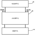
如图2所示,本发明实施例提供一种振荡器,包括谐振单元10、交叉耦合的电流源单元30以及耦合在上述电流源单元30和谐振单元10之间的正反馈单元20;其中,该谐振单元10,用于产生具有第一振荡频率 的差分振荡信号;正反馈单元20,用于接收上述差分振荡信号,并对上述差分振荡信号做增益增强得到差分输出振荡信号;电流源单元30用于为谐振单元10和正反馈单元20提供可调偏置电流。在正反馈单元和电流源单元之间设置有差分振荡信号输出端(即图2中所示的正向差分振荡信号输出端OUTP和负向差分振荡信号输出端OUTN),用于输出差分输出振荡信号,其中,OUTP用于连接负载,并为负载输出正向差分输出振荡信号,OUTN用于为负载输出负向差分输出振荡信号。具体的,电流源单元30通过正反馈单元20为谐振单元10提供可调偏置电流。As shown in FIG. 2, an embodiment of the present invention provides an oscillator including a resonating unit 10, a cross-coupled current source unit 30, and a positive feedback unit 20 coupled between the current source unit 30 and the resonating unit 10; The resonant unit 10 is configured to generate a first oscillation frequency The differential oscillating signal 20 is configured to receive the differential oscillating signal and perform gain enhancement on the differential oscillating signal to obtain a differential output oscillating signal; the current source unit 30 is configured to provide an adjustable tunable unit 10 and the positive feedback unit 20 Bias current. A differential oscillation signal output terminal (ie, a forward differential oscillation signal output terminal OUTP and a negative differential oscillation signal output terminal OUTN shown in FIG. 2) is disposed between the positive feedback unit and the current source unit for outputting differential output oscillation The signal, where OUTP is used to connect the load, and outputs a positive differential output oscillating signal for the load, and OUTN is used to output a negative differential output oscillating signal for the load. Specifically, the current source unit 30 provides the tunable bias current to the resonant unit 10 through the positive feedback unit 20.
本发明实施例提供一种振荡器,由于电流源单元可以为正反馈单元和谐振单元提供可调偏置电流,并与正反馈单元构成Gm-boosted(跨导增强)结构,使得正反馈单元能够对接收到的差分振荡信号做增益增强得到差分输出振荡信号,因此,可以在保证振荡器正常启动的条件下,通过减小偏置电流,降低本发明实施例提供的振荡器的功耗。The embodiment of the invention provides an oscillator, wherein the current source unit can provide a tunable bias current for the positive feedback unit and the resonance unit, and form a Gm-boosted structure with the positive feedback unit, so that the positive feedback unit can The gain enhancement is performed on the received differential oscillating signal to obtain a differential output oscillating signal. Therefore, the power consumption of the oscillator provided by the embodiment of the present invention can be reduced by reducing the bias current under the condition that the oscillator is normally started.
可选的,该谐振单元10,还用于经正反馈单元20将差分振荡信号输出到电流源单元30;电流源单元30,还用于根据谐振单元10输出的差分振荡信号,通过控制偏置电压的大小调整偏置电流,以调整差分输出振荡信号的幅度。Optionally, the resonant unit 10 is further configured to output the differential oscillating signal to the current source unit 30 via the positive feedback unit 20; the current source unit 30 is further configured to control the bias according to the differential oscillating signal output by the resonant unit 10. The magnitude of the voltage adjusts the bias current to adjust the amplitude of the differential output oscillating signal.
由于振荡器中的谐振单元10输出的差分振荡信号的幅度等于该振荡器中的电流源单元30为谐振单元10和正反馈单元20提供的偏置电流与该振荡器中的电阻(即该振荡器中所有器件的等效阻抗)的乘积,且该振荡器中的电阻的值几乎不变,故该差分振荡信号的幅度与电流源单元提供的偏置电流成正比,又因为该偏置电流的大小与偏置电压的大小成正比,因此,本发明实施例可以通过调整偏置电压的大小改变振荡器中的偏置电流的大小。Since the amplitude of the differential oscillating signal output by the resonant unit 10 in the oscillator is equal to the bias current provided by the current source unit 30 in the oscillator for the resonant unit 10 and the positive feedback unit 20 and the resistance in the oscillator (ie, the oscillator) The product of the equivalent impedance of all devices, and the value of the resistor in the oscillator is almost constant, so the amplitude of the differential oscillating signal is proportional to the bias current provided by the current source unit, and because of the bias current The size is proportional to the magnitude of the bias voltage, and thus embodiments of the present invention can vary the magnitude of the bias current in the oscillator by adjusting the magnitude of the bias voltage.
具体的,若振荡器(具体为振荡器中的谐振单元10)输出的差分振荡信号的幅度过大,可以通过控制该偏置电压变小,以减小偏置电流,从而降低振荡器输出的该差分振荡信号的幅度,若振荡器输出的差分振荡信号的幅度过小,可以控制该偏置电压变大,增大偏置电流,以提高振荡器输出的差分振荡信号的幅度,最终使得振荡器输出的差分振荡信 号的幅度稳定。Specifically, if the amplitude of the differential oscillating signal output by the oscillator (specifically, the resonant unit 10 in the oscillator) is too large, the bias voltage can be reduced to reduce the bias current, thereby reducing the oscillator output. The amplitude of the differential oscillating signal, if the amplitude of the differential oscillating signal output by the oscillator is too small, the bias voltage can be controlled to be large, and the bias current is increased to increase the amplitude of the differential oscillating signal output by the oscillator, and finally the oscillation Differential oscillation signal The magnitude of the number is stable.
如图3所示,本发明实施例提供的正反馈单元20包括:第一金属氧化物半导体MOS管M1、第二MOS管M2、第一电容C1、第二电容C2、第三电容C3以及第四电容C4;其中,第一MOS管M1的第一极101作为第一输出节点分别与谐振单元10的第一端及第一电容C1的一端连接,第一MOS管M1的第二极102分别与第一电容C1的另一端及第三电容C3的一端连接,第一MOS管M1的栅极和第二MOS管M2的栅极均与第一恒定电压源103连接,第二MOS管M2的第一极201作为第二输出节点分别与谐振单元10的第二端及第二电容C2的一端连接,第二MOS管M2的第二极202分别与第二电容C2的另一端及第四电容C4的一端连接,第四电容C4的另一端和第三电容C3的另一端连接,第三电容C3的一端和第四电容C4的一端均与电流源单元30连接,在第三电容C3的一端与电流源单元30的第三输出节点之间设置有正向差分信号输出端OUTP,在第四电容C4的一端与电流源单元30的第四输出节点之间设置有负向差分信号输出端OUTN。As shown in FIG. 3, the positive feedback unit 20 provided by the embodiment of the present invention includes: a first metal oxide semiconductor MOS transistor M1, a second MOS transistor M2, a first capacitor C1, a second capacitor C2, a third capacitor C3, and a first a fourth capacitor C4; wherein the first pole 101 of the first MOS transistor M1 is connected as a first output node to the first end of the resonant unit 10 and one end of the first capacitor C1, respectively, and the second pole 102 of the first MOS transistor M1 is respectively Connected to the other end of the first capacitor C1 and one end of the third capacitor C3, the gate of the first MOS transistor M1 and the gate of the second MOS transistor M2 are both connected to the first constant voltage source 103, and the second MOS transistor M2 The first pole 201 is connected to the second end of the resonant unit 10 and one end of the second capacitor C2 as a second output node, and the second pole 202 of the second MOS transistor M2 is respectively connected to the other end of the second capacitor C2 and the fourth capacitor. One end of the C4 is connected, the other end of the fourth capacitor C4 is connected to the other end of the third capacitor C3, and one end of the third capacitor C3 and one end of the fourth capacitor C4 are connected to the current source unit 30 at one end of the third capacitor C3. A forward differential signal output terminal OUTP is disposed between the third output node of the current source unit 30, A negative differential signal output terminal OUTN is provided between one end of the fourth capacitor C4 and the fourth output node of the current source unit 30.
本发明实施例中通过正反馈单元20中的第一MOS管M1和第二MOS管M2为振荡器振荡时提供启动增益,并通过第一电容C1、第一MOS管M1与第三电容C3、第二电容C2、第二MOS管M2与第四电容C4构成交流正反馈,将该振荡器中的器件噪声放大,使得该振荡器维持振荡状态,并通过正向差分信号输出端OUTP和负向差分信号输出端OUTN输出差分输出振荡信号。并且,由于第一MOS管M1和第二MOS管M2的栅极接第一恒定电压源103,且第一MOS管M1的第一极101和第二极102分别与第一电容C1的一端和另一端相连,第二MOS管的第一极201和第二极202分别与第二电容C2的一端和另一端相连,因此,只有当差分输出振荡信号的电压小于第一恒定电压源103的电压时,第一MOS管M1和第二MOS管M2才导通,这样缩短了一个振荡周期内第一MOS管M1和第二MOS管M2的导通时间,即一个振荡周期内电流源单元30和正反馈单元20向谐振单元10中注入电流噪声的时间变短,所以与现有技术相比,在一个振荡周期内该振荡器中的相位噪声(由电流噪声转化得到)较低。 In the embodiment of the present invention, the first MOS transistor M1 and the second MOS transistor M2 in the positive feedback unit 20 provide a startup gain when the oscillator oscillates, and pass through the first capacitor C1, the first MOS transistor M1 and the third capacitor C3, The second capacitor C2, the second MOS transistor M2 and the fourth capacitor C4 form an alternating current positive feedback, and the device noise in the oscillator is amplified, so that the oscillator maintains an oscillating state, and passes through the forward differential signal output terminal OUTP and the negative direction. The differential signal output terminal OUTN outputs a differential output oscillation signal. Moreover, since the gates of the first MOS transistor M1 and the second MOS transistor M2 are connected to the first constant voltage source 103, and the first pole 101 and the second pole 102 of the first MOS transistor M1 are respectively connected to one end of the first capacitor C1. Connected to the other end, the first pole 201 and the second pole 202 of the second MOS transistor are respectively connected to one end and the other end of the second capacitor C2, so that only when the voltage of the differential output oscillating signal is smaller than the voltage of the first constant voltage source 103 When the first MOS transistor M1 and the second MOS transistor M2 are turned on, the ON time of the first MOS transistor M1 and the second MOS transistor M2 in one oscillation period is shortened, that is, the current source unit 30 and the positive during one oscillation period. The time during which the feedback unit 20 injects current noise into the resonance unit 10 becomes shorter, so that the phase noise (converted from current noise) in the oscillator is lower in one oscillation period than in the prior art.
该第一恒定电压源103可以为第一电源,也可以为其他恒定电压源,本发明实施例对此不进行限制,可以根据需要进行选择。The first constant voltage source 103 may be a first power source or other constant voltage source. The embodiment of the present invention does not limit this, and may be selected as needed.
进一步,由于本发明实施例提供的振荡器,通过利用第一电容C1和第二电容C2的相移特性使得差分振荡信号的电压的波形和电流的波形之间存在90度相移特性,如此,使得一个振荡周期内,噪声调制函数NMF的最大值对应ISF的最小值,根据公式Γeff(ωt)=Γ(ωt)×α(ωt),Γeff(ωt)为ISFeff,Γ(ωt)为ISF,α(ωt)为相位随时间变化的NMF,可以在一个振荡周期内减小ISFeff的值,从而进一步降低本发明实施例提供的振荡器的相位噪声。Further, the oscillator provided by the embodiment of the present invention has a phase shift characteristic of the first capacitor C1 and the second capacitor C2 such that a waveform of a voltage of the differential oscillation signal and a waveform of the current have a phase shift characteristic of 90 degrees. In a period of oscillation, the maximum value of the noise modulation function NMF corresponds to the minimum value of the ISF, according to the formula Γ eff (ωt) = Γ (ωt) × α (ωt), Γ eff (ωt) is ISF eff , Γ (ωt) For ISF, α(ωt) is the NMF whose phase changes with time, and the value of ISF eff can be reduced in one oscillation period, thereby further reducing the phase noise of the oscillator provided by the embodiment of the present invention.
进一步地,由于电流源单元30可以为正反馈单元20和谐振单元10提供可调偏置电流,并与正反馈单元20构成Gm-boosted(跨导增强)结构,因此,可以在保证振荡器正常启动的条件下,通过减小偏置电流,可以降低本发明实施例提供的振荡器的功耗。Further, since the current source unit 30 can provide the tunable bias current for the positive feedback unit 20 and the resonance unit 10, and form a Gm-boosted structure with the positive feedback unit 20, the oscillator can be guaranteed to be normal. Under the condition of startup, the power consumption of the oscillator provided by the embodiment of the present invention can be reduced by reducing the bias current.
可选的,结合图3,如图4a所示,本发明实施例中的电流源单元30包括:第三MOS管M3、第四MOS管M4、第五电容C5、第六电容C6、第一电阻R1以及第二电阻R2;其中,第三MOS管M3的栅极分别与第六电容C6的一端及第一电阻R1的一端连接,第三MOS管M3的漏极作为第三输出节点分别与第五电容C5的一端及第三电容C3的一端连接;该第四MOS管M4的栅极分别与第五电容C5的另一端及第二电阻R2的一端连接,第四MOS管M4的漏极作为第四输出节点分别与第六电容C6的另一端及第四电容C4的一端连接;第一电阻R1的另一端和第二电阻R2的另一端均与可调电源Vb连接,该可调电源Vb用于为电流源单元30提供可调偏置电压,该电流源单元30具体用于通过该可调电源Vb为谐振单元10和正反馈单元20提供可调偏置电流;第三MOS管M3的源极和第四MOS管M4的源极与第二恒定电压节点104连接。第三MOS管M3和第四MOS管M4是PMOS管。电流源单元30的工作原理类似于考毕兹(colpitts)振荡器。Optionally, in conjunction with FIG. 3, as shown in FIG. 4a, the current source unit 30 in the embodiment of the present invention includes: a third MOS transistor M3, a fourth MOS transistor M4, a fifth capacitor C5, a sixth capacitor C6, and a first a resistor R1 and a second resistor R2; wherein a gate of the third MOS transistor M3 is respectively connected to one end of the sixth capacitor C6 and one end of the first resistor R1, and the drain of the third MOS transistor M3 serves as a third output node respectively One end of the fifth capacitor C5 and one end of the third capacitor C3 are connected; the gate of the fourth MOS transistor M4 is respectively connected to the other end of the fifth capacitor C5 and one end of the second resistor R2, and the drain of the fourth MOS transistor M4 As the fourth output node, respectively connected to the other end of the sixth capacitor C6 and one end of the fourth capacitor C4; the other end of the first resistor R1 and the other end of the second resistor R2 are connected to the adjustable power source Vb, the adjustable power source Vb is used to provide a tunable bias voltage for the current source unit 30. The current source unit 30 is specifically configured to provide the tunable bias current for the resonant unit 10 and the positive feedback unit 20 through the adjustable power supply Vb; the third MOS transistor M3 The source and the source of the fourth MOS transistor M4 are connected to the second constant voltage node 104. The third MOS transistor M3 and the fourth MOS transistor M4 are PMOS transistors. The current source unit 30 operates similarly to a Colpitts oscillator.
可替换地,如果第三MOS管M3和第四MOS管M4是NMOS(Negative Channel Metal Oxide Semiconductor,N型沟道金属氧化物半导体)管,则第三MOS管的源极和第四MOS管的源极均接地。 此时第一MOS管M1和第二MOS管M2可以是NMOS管,也可以是PMOS管。Alternatively, if the third MOS transistor M3 and the fourth MOS transistor M4 are NMOS (Negative Channel Metal Oxide Semiconductor) tubes, the source of the third MOS transistor and the fourth MOS transistor The sources are all grounded. At this time, the first MOS transistor M1 and the second MOS transistor M2 may be an NMOS transistor or a PMOS transistor.
可替换地,如果第三MOS管M3和第四MOS管M4为PMOS(Positive Channel Metal Oxide Semiconductor,P型沟道金属氧化物半导体)管,此时,第三MOS管的源极和第四MOS管的源极均接第一电源,此时,第一MOS管M1和第二MOS管M2可以为PMOS管,也可以为NMOS管。Alternatively, if the third MOS transistor M3 and the fourth MOS transistor M4 are PMOS (Positive Channel Metal Oxide Semiconductor) tubes, at this time, the source of the third MOS transistor and the fourth MOS The source of the tube is connected to the first power source. At this time, the first MOS transistor M1 and the second MOS transistor M2 may be a PMOS transistor or an NMOS transistor.
如图4a所示的振荡器,本发明实施例提供的振荡器包括四个MOS管,即第一MOS管M1、第二MOS管M2、第三MOS管M3以及第四MOS管M4,这四个MOS管共同构成Gm-boosted(跨导增强)结构,一方面,可以功耗在相同的情况下,得到较高的启动增益;另一方面,可以在相同启动增益情况下,得到较小的功耗,而现有技术(如图1a所示的Cross coupled负阻振荡器)只有两个MOS管即如图1a所示的M1和M2,当图4a所示的振荡器和图1a所示的Cross coupled负阻振荡器具有相同的启动增益时,图1a所示的Cross coupled负阻振荡器需要消耗更多的电流满足上述启动增益,由于振荡器的功耗与电流成正比,因此本发明实施例如图4a所示的振荡器的功耗低于现有技术。As shown in FIG. 4a, the oscillator provided by the embodiment of the present invention includes four MOS transistors, namely, a first MOS transistor M1, a second MOS transistor M2, a third MOS transistor M3, and a fourth MOS transistor M4. The MOS transistors together form a Gm-boosted structure. On the one hand, the power consumption can be higher under the same conditions, and on the other hand, the same startup gain can be obtained. Power consumption, while the prior art (such as the Cross-coupled negative-resistance oscillator shown in Figure 1a) has only two MOS transistors, M1 and M2 as shown in Figure 1a, as shown in Figure 4a and Figure 1a. When the Cross-coupled negative-resistance oscillator has the same startup gain, the Cross-coupled negative-resistance oscillator shown in FIG. 1a needs to consume more current to satisfy the above-mentioned startup gain. Since the power consumption of the oscillator is proportional to the current, the present invention The power consumption of implementing an oscillator such as that shown in Figure 4a is lower than in the prior art.
一方面,在如图4a所示的振荡器中,第五电容C5和第六电容C6的作用主要是将第三MOS管M3和第四MOS管M4的栅极直流电压和正反馈单元20输出的直流电压隔离,从而避免正反馈单元20输出的直流电压对第三MOS管M3和第四MOS管M4造成影响。On the one hand, in the oscillator shown in FIG. 4a, the fifth capacitor C5 and the sixth capacitor C6 mainly function to output the gate DC voltage of the third MOS transistor M3 and the fourth MOS transistor M4 and the positive feedback unit 20. The DC voltage is isolated to prevent the DC voltage output from the positive feedback unit 20 from affecting the third MOS transistor M3 and the fourth MOS transistor M4.
另一方面,如图4a所示的振荡器中,可以通过控制可调电源Vb的输出的电压大小,调整第三MOS管M3和第四MOS管M4处于不同的工作模式,例如,可以将第三MOS管M3和第四MOS管M4的工作模式,从当前工作模式调整为第一工作模式,从而使得电流源单元30为谐振单元10和正反馈单元20提供可调偏置电流。On the other hand, in the oscillator shown in FIG. 4a, the third MOS transistor M3 and the fourth MOS transistor M4 can be adjusted to different operating modes by controlling the voltage magnitude of the output of the adjustable power supply Vb, for example, The operating modes of the three MOS transistors M3 and the fourth MOS transistor M4 are adjusted from the current operating mode to the first operating mode such that the current source unit 30 provides the tunable bias current for the resonant unit 10 and the positive feedback unit 20.
本发明实施例中,上述第一工作模式包括但不限于A类(Class A)工作模式(又称为甲类工作模式)、B类(Class B)工作模式(又称为乙类工作模式)、C类(Class C)工作模式(又称为丙类工作模式)、D 类(Class D)工作模式(又称为丁类工作模式)和E类(Class E)工作模式。即本发明实施例提供的振荡器中,上述第一工作模式除了以上五类工作模式之外,还可以是其他满足使用需求的工作模式,例如AB类(Class AB)工作模式(又称为甲乙类工作模式)。In the embodiment of the present invention, the first working mode includes, but is not limited to, a class A working mode (also referred to as a class A working mode) and a class B (class B) working mode (also referred to as a class B working mode). , Class C (Class C) working mode (also known as Class C working mode), D Class (Class D) working mode (also known as D-class working mode) and Class E (Class E) working mode. In the oscillator provided by the embodiment of the present invention, in addition to the above five working modes, the first working mode may be another working mode that satisfies the use requirement, for example, a Class AB working mode (also referred to as A and B). Class working mode).
示例性的,当本发明实施例中的第一工作模式为A类工作模式,即电流源单元30中的第三MOS管M3和第四MOS管M4工作在A类工作模式下时,在一个振荡周期内,电流源单元30中的第三MOS管M3、第四MOS管M4均导通,但是由于第一MOS管的栅极接第一恒定电压源103,第二MOS管的栅极接第一恒定电压源103,该第一恒定电压源为可调电源,只有当第一MOS管M1和第二MOS管M2的栅源电压差的绝对值大于第一MOS管M1和第二MOS管M2的阈值电压(也即开启电压UGS(th)的绝对值)时,第一MOS管M1和第二MOS管M2才导通,也即正反馈单元输出的正向差分输出振荡信号的幅度和负向差分输出振荡信号的幅度分别与第一MOS管M1和第二MOS管M2的栅极电压差的绝对值大于阈值电压时,第一MOS管M1和第二MOS管M2才导通,本发明实施例中,因此,在一个振荡周期内当第三MOS管M3和第四MOS管M4均导通时,第一MOS管M1和第二MOS管M2的工作状态处在C类工作模式或者比C类工作模式更深的工作模式(例如,D类工作模式,E类工作模式)。Exemplarily, when the first working mode in the embodiment of the present invention is a class A working mode, that is, the third MOS transistor M3 and the fourth MOS transistor M4 in the current source unit 30 operate in the class A working mode, in one During the oscillation period, the third MOS transistor M3 and the fourth MOS transistor M4 in the current source unit 30 are both turned on, but since the gate of the first MOS transistor is connected to the first constant voltage source 103, the gate of the second MOS transistor is connected. a first constant voltage source 103, the first constant voltage source being an adjustable power supply, only when the absolute value of the gate-source voltage difference between the first MOS transistor M1 and the second MOS transistor M2 is greater than the first MOS transistor M1 and the second MOS transistor When the threshold voltage of M2 (that is, the absolute value of the turn-on voltage UGS(th)) is turned on, the first MOS transistor M1 and the second MOS transistor M2 are turned on, that is, the amplitude of the forward differential output oscillating signal output by the positive feedback unit. When the amplitudes of the negative differential output oscillation signals and the gate voltage difference between the first MOS transistor M1 and the second MOS transistor M2 are greater than the threshold voltage, respectively, the first MOS transistor M1 and the second MOS transistor M2 are turned on, In the embodiment of the invention, therefore, when both the third MOS transistor M3 and the fourth MOS transistor M4 are turned on in one oscillation period, the first MOS transistor M1 The working state of the second MOS transistor M2 is in the C-type working mode or the working mode deeper than the C-type working mode (for example, the D-type working mode, the E-type working mode).
当本发明实施例中的第一工作模式为B类工作模式,即电流源单元30中的第三MOS管M3和第四MOS管M4工作在B类工作模式下时,在一个振荡周期的前1/2周期内,第三MOS管M3导通,由于第二MOS管的源极接第三MOS管的栅极,因此,当第二MOS管M2的栅源电压差的绝对值大于第二MOS管M2阈值电压时,第二MOS管M2导通,当第二MOS管M2的栅源电压差的绝对值小于第二MOS管M2阈值电压时,第二MOS管M2截止;第四MOS管M4截止,第一MOS管M1截止;在该振荡周期的后1/2周期内,第三MOS管M3截止,第二MOS管M2截止;第四MOS管M4导通,当第一MOS管M1的栅源电压差的绝对值大于第一MOS管M1阈值电压时,第一MOS管M1导 通。或者,在一个振荡周期的前1/2周期内,第四MOS管M4导通,当第一MOS管M1的栅源电压差大于第一MOS管M1的阈值电压时,第一MOS管M1导通,第三MOS管M3截止,第二MOS管M2截止;在该振荡周期的后1/2周期内,第四MOS管M4截止,第一MOS管M1截止,第三MOS管M3导通,当第二MOS管M2的栅源电压差的绝对值大于第二MOS管M2的阈值电压时,第二MOS管M2导通。When the first working mode in the embodiment of the present invention is a class B working mode, that is, the third MOS transistor M3 and the fourth MOS transistor M4 in the current source unit 30 operate in the class B working mode, before an oscillation period. In the 1/2 period, the third MOS transistor M3 is turned on, and since the source of the second MOS transistor is connected to the gate of the third MOS transistor, when the absolute value of the gate-source voltage difference of the second MOS transistor M2 is greater than the second When the MOS transistor M2 has a threshold voltage, the second MOS transistor M2 is turned on, and when the absolute value of the gate-source voltage difference of the second MOS transistor M2 is smaller than the threshold voltage of the second MOS transistor M2, the second MOS transistor M2 is turned off; the fourth MOS transistor M4 is turned off, the first MOS transistor M1 is turned off; in the second 1/2 period of the oscillation period, the third MOS transistor M3 is turned off, the second MOS transistor M2 is turned off; the fourth MOS transistor M4 is turned on, when the first MOS transistor M1 is turned on When the absolute value of the gate-source voltage difference is greater than the threshold voltage of the first MOS transistor M1, the first MOS transistor M1 leads through. Alternatively, the fourth MOS transistor M4 is turned on during the first 1/2 period of an oscillation period. When the gate-source voltage difference of the first MOS transistor M1 is greater than the threshold voltage of the first MOS transistor M1, the first MOS transistor M1 is turned on. The third MOS transistor M3 is turned off, and the second MOS transistor M2 is turned off. During the second half of the oscillation period, the fourth MOS transistor M4 is turned off, the first MOS transistor M1 is turned off, and the third MOS transistor M3 is turned on. When the absolute value of the gate-source voltage difference of the second MOS transistor M2 is greater than the threshold voltage of the second MOS transistor M2, the second MOS transistor M2 is turned on.
当本发明实施例中的第一工作模式为C类工作模式,即电流源单元30中的第三MOS管M3和第四MOS管M4工作在C类工作模式下时,在一个振荡周期的前1/3周期内,第三MOS管M3导通,由于第二MOS管M2的源极与第三MOS管M3的栅极连接,因此,当第二MOS管的栅源电压差的绝对值大于第二MOS管M2的阈值电压时,第二MOS管M2导通,第四MOS管M4截止,由于第一MOS管M1的源极接第四MOS管M4的栅极,因此,第一MOS管M1截止;在该振荡周期的后2/3周期内,第三MOS管M3截止,由于第二MOS管M2的源极与第三MOS管M3的栅极连接,因此,当第三MOS管M3截止时,第二MOS截止,第四MOS管M4导通,由于第二MOS管的源极接第四MOS管的栅极,因此,当第一MOS管M1的栅源电压差的绝对值大于第一MOS管M1的阈值电压时,第一MOS管M1导通。或者,在一个振荡周期的前1/3周期内,第四MOS管M4导通,当第一MOS管M1的栅源电压差的绝对值大于第一MOS管M1的阈值电压时,第一MOS管M1导通;第三MOS管M3截止,第二MOS管M2截止;在该振荡周期的后2/3周期内,第四MOS管M4截止,第一MOS管M1截止,第三MOS管M3导通,当第二MOS管M2的栅源电压差的绝对值大于阈值电压时,第二MOS管M2导通。When the first working mode in the embodiment of the present invention is the C-type working mode, that is, the third MOS transistor M3 and the fourth MOS transistor M4 in the current source unit 30 operate in the C-type working mode, before one oscillation period In the 1/3 period, the third MOS transistor M3 is turned on, and since the source of the second MOS transistor M2 is connected to the gate of the third MOS transistor M3, when the absolute value of the gate-source voltage difference of the second MOS transistor is greater than When the threshold voltage of the second MOS transistor M2 is reached, the second MOS transistor M2 is turned on, and the fourth MOS transistor M4 is turned off. Since the source of the first MOS transistor M1 is connected to the gate of the fourth MOS transistor M4, the first MOS transistor M1 is turned off; in the second 2/3 cycle of the oscillation period, the third MOS transistor M3 is turned off, and since the source of the second MOS transistor M2 is connected to the gate of the third MOS transistor M3, when the third MOS transistor M3 When the second MOS is turned off, the fourth MOS transistor M4 is turned on, and since the source of the second MOS transistor is connected to the gate of the fourth MOS transistor, when the absolute value of the gate-source voltage difference of the first MOS transistor M1 is greater than When the threshold voltage of the first MOS transistor M1 is reached, the first MOS transistor M1 is turned on. Alternatively, in the first 1/3 period of one oscillation period, the fourth MOS transistor M4 is turned on, and when the absolute value of the gate-source voltage difference of the first MOS transistor M1 is greater than the threshold voltage of the first MOS transistor M1, the first MOS The tube M1 is turned on; the third MOS transistor M3 is turned off, and the second MOS transistor M2 is turned off; in the second 2/3 period of the oscillation period, the fourth MOS transistor M4 is turned off, the first MOS transistor M1 is turned off, and the third MOS transistor M3 is turned off. Turning on, when the absolute value of the gate-source voltage difference of the second MOS transistor M2 is greater than the threshold voltage, the second MOS transistor M2 is turned on.
当本发明实施例中的第一工作模式为D类工作模式,即电流源单元30中的第三MOS管M3和第四MOS管M4工作在D类工作模式下时,在一个振荡周期的前1/4周期内,第四MOS管M4截止,第一MOS管截止,第三MOS管M3导通,当第二MOS管M2的栅源电压差的绝对值大于阈值电压时,第二MOS管M2导通;在该振荡周期的后3/4周 期内,第三MOS管M3截止,第二MOS管M2截止,第四MOS管M4导通,当第一MOS管M1的栅源电压差的绝对值大于第一MOS管M1的阈值电压时,第一MOS管M1导通。或者在一个振荡周期的前1/4周期内,第三MOS管M3截止,第二MOS管M2截止,第四MOS管M4导通,当第一MOS管M1的栅源电压大于第一MOS管M1的阈值电压时,第一MOS管M1导通;在该振荡周期的后3/4周期内,第四MOS管M4截止,第一MOS管M1截止,第三MOS管M3导通,当第二MOS管M2的栅源电压差的绝对值大于第二MOS管M2的阈值电压时,第二MOS管M2导通。When the first working mode in the embodiment of the present invention is the D-type working mode, that is, the third MOS transistor M3 and the fourth MOS transistor M4 in the current source unit 30 operate in the D-type working mode, before an oscillation period In the 1/4 cycle, the fourth MOS transistor M4 is turned off, the first MOS transistor is turned off, and the third MOS transistor M3 is turned on. When the absolute value of the gate-source voltage difference of the second MOS transistor M2 is greater than the threshold voltage, the second MOS transistor M2 is on; 3/4 weeks after the oscillation period During the period, the third MOS transistor M3 is turned off, the second MOS transistor M2 is turned off, and the fourth MOS transistor M4 is turned on. When the absolute value of the gate-source voltage difference of the first MOS transistor M1 is greater than the threshold voltage of the first MOS transistor M1, The first MOS transistor M1 is turned on. Or in the first quarter cycle of an oscillation period, the third MOS transistor M3 is turned off, the second MOS transistor M2 is turned off, and the fourth MOS transistor M4 is turned on, when the gate-source voltage of the first MOS transistor M1 is larger than the first MOS transistor When the threshold voltage of M1 is reached, the first MOS transistor M1 is turned on; in the last 3/4 period of the oscillation period, the fourth MOS transistor M4 is turned off, the first MOS transistor M1 is turned off, and the third MOS transistor M3 is turned on. When the absolute value of the gate-source voltage difference of the second MOS transistor M2 is greater than the threshold voltage of the second MOS transistor M2, the second MOS transistor M2 is turned on.
当本发明实施例中的第一工作模式为E类工作模式,即电流源单元30中的第三MOS管M3和第四MOS管M4工作在E类工作模式下时,在一个振荡周期的前1/5周期内,第四MOS管M4截止,第一MOS管M1截止,第三MOS管M3导通,当第二MOS管M2的栅源电压差的绝对值大于第二MOS管M2的阈值电压时,第二MOS管M2导通;在该振荡周期的后4/5周期内,第三MOS管M3截止,第二MOS管M1截止,第四MOS管M4导通,当第一MOS管M1的栅源电压差的绝对值大于第一MOS管M1的阈值电压时,第一MOS管M1导通。或者在一个振荡周期的前1/5周期内,第三MOS管M3截止,第二MOS管M2截止,第四MOS管M4导通,当第一MOS管M1的栅源电压差的绝对值大于第一MOS管M1的阈值电压时,第一MOS管M1导通;在该振荡周期的后4/5周期内,第四MOS管M4截止,第一MOS管M1截止,第三MOS管M3导通,当第二MOS管M2的栅源电压差的绝对值大于第二MOS管M2的阈值电压时,第二MOS管M2导通。When the first working mode in the embodiment of the present invention is the E-type working mode, that is, the third MOS transistor M3 and the fourth MOS transistor M4 in the current source unit 30 operate in the E-type working mode, before an oscillation period In the 1/5 cycle, the fourth MOS transistor M4 is turned off, the first MOS transistor M1 is turned off, and the third MOS transistor M3 is turned on. When the absolute value of the gate-source voltage difference of the second MOS transistor M2 is greater than the threshold of the second MOS transistor M2 When the voltage is applied, the second MOS transistor M2 is turned on; during the last 4/5 cycles of the oscillation period, the third MOS transistor M3 is turned off, the second MOS transistor M1 is turned off, and the fourth MOS transistor M4 is turned on, when the first MOS transistor is turned on. When the absolute value of the gate-source voltage difference of M1 is larger than the threshold voltage of the first MOS transistor M1, the first MOS transistor M1 is turned on. Or in the first 1/5 cycle of an oscillation period, the third MOS transistor M3 is turned off, the second MOS transistor M2 is turned off, and the fourth MOS transistor M4 is turned on, when the absolute value of the gate-source voltage difference of the first MOS transistor M1 is greater than When the threshold voltage of the first MOS transistor M1 is reached, the first MOS transistor M1 is turned on; during the last 4/5 cycles of the oscillation period, the fourth MOS transistor M4 is turned off, the first MOS transistor M1 is turned off, and the third MOS transistor M3 is turned on. When the absolute value of the gate-source voltage difference of the second MOS transistor M2 is greater than the threshold voltage of the second MOS transistor M2, the second MOS transistor M2 is turned on.
需要说明的是,当本发明实施例中的第一工作模式为上述所描述的A类工作模式、B类工作模式、C类工作模式、D类工作模式以及E类工作模式之外的其他工作模式时,在该工作模式下,在一个振荡周期的前1/M周期,第四MOS管M4截止,第一MOS管M1截止,第三MOS管M3导通,当第二MOS管M2的栅源电压差的绝对值大于第二MOS管M2的阈值电压时,第二MOS管M2导通;在该振荡周期的后(M-1) /M个周期,第三MOS管M3截止,第二MOS管M2截止,第四MOS管M4导通,当第一MOS管M1的栅源电压差的绝对值大于第一MOS管M1的阈值电压时,第一MOS管M1导通。或者,在一个振荡周期的前1/M周期,第三MOS管M3截止,第二MOS管M2截止,第四MOS管M4导通,当第一MOS管M1的栅源电压差的绝对值大于第一MOS管M1的阈值电压时,第一MOS管M1导通;在该振荡周期的后(M-1)/M个周期,第四MOS管M4截止,第一MOS管M1截止,第三MOS管M3导通,当第二MOS管M2的栅源电压差的绝对值大于第二MOS管M2的阈值电压时,第二MOS管M2导通。It should be noted that, when the first working mode in the embodiment of the present invention is the above-described work of the class A working mode, the class B working mode, the class C working mode, the class D working mode, and the class E working mode, In the mode, in the operation mode, in the first 1/M period of one oscillation period, the fourth MOS transistor M4 is turned off, the first MOS transistor M1 is turned off, and the third MOS transistor M3 is turned on, when the gate of the second MOS transistor M2 is turned on. When the absolute value of the source voltage difference is greater than the threshold voltage of the second MOS transistor M2, the second MOS transistor M2 is turned on; after the oscillation period (M-1) /M cycles, the third MOS transistor M3 is turned off, the second MOS transistor M2 is turned off, and the fourth MOS transistor M4 is turned on, when the absolute value of the gate-source voltage difference of the first MOS transistor M1 is greater than the threshold voltage of the first MOS transistor M1 At the time, the first MOS transistor M1 is turned on. Alternatively, in the first 1/M period of one oscillation period, the third MOS transistor M3 is turned off, the second MOS transistor M2 is turned off, and the fourth MOS transistor M4 is turned on, when the absolute value of the gate-source voltage difference of the first MOS transistor M1 is greater than When the threshold voltage of the first MOS transistor M1 is reached, the first MOS transistor M1 is turned on; after (M-1)/M cycles of the oscillation period, the fourth MOS transistor M4 is turned off, and the first MOS transistor M1 is turned off, and the third The MOS transistor M3 is turned on, and when the absolute value of the gate-source voltage difference of the second MOS transistor M2 is greater than the threshold voltage of the second MOS transistor M2, the second MOS transistor M2 is turned on.
可选的,通常情况下,上述正反馈单元20在工作时,为了满足巴克豪森(Barkhausen)准则,该正反馈单元20中的第一MOS管M1和第二MOS管需要具有较高的跨导来满足振荡电路启动增益的要求,这样第一MOS管M1和第二MOS管M2便需要消耗更多的电流,从而导致振荡器的功耗比较大。本发明实施例中,为了降低本发明实施例提供的振荡器的功耗,可以通过调整偏置电压Vb的大小将第三MOS管和第四MOS管的工作模式设置为C类工作模式或者比C类工作模式更深的工作模式(即第三MOS管和第四MOS管的导通时间小于第三MOS管和第四MOS管在C类工作模式下的导通时间),以使得电流源单元30为本发明实施例提供的振荡器中的正反馈单元20和谐振单元10提供偏置电流和启动增益。通过该方案,由于可以通过缩短有源器件导通的时间来减小RMS(Root Mean Square,均方根值)电流,因此能够提高电流效率,从而达到在低功耗的情况下获得优越的相位噪声性能的目的。Optionally, in general, when the positive feedback unit 20 is in operation, in order to meet the Barkhausen criterion, the first MOS tube M1 and the second MOS tube in the positive feedback unit 20 need to have a higher cross. The first MOS transistor M1 and the second MOS transistor M2 need to consume more current, so that the power consumption of the oscillator is relatively large. In the embodiment of the present invention, in order to reduce the power consumption of the oscillator provided by the embodiment of the present invention, the working modes of the third MOS transistor and the fourth MOS transistor may be set to the C-type working mode or ratio by adjusting the magnitude of the bias voltage Vb. The C mode of operation has a deeper working mode (ie, the conduction time of the third MOS transistor and the fourth MOS transistor is smaller than the conduction time of the third MOS transistor and the fourth MOS transistor in the C mode of operation), so that the current source unit The positive feedback unit 20 and the resonant unit 10 in the oscillator provided by the embodiment of the present invention provide a bias current and a starting gain. With this scheme, since the RMS (Root Mean Square) current can be reduced by shortening the time during which the active device is turned on, current efficiency can be improved, thereby achieving superior phase in the case of low power consumption. The purpose of noise performance.
本发明实施例中通过正反馈单元20中的第一MOS管M1和第二MOS管M2为振荡器振荡时提供启动增益,并通过第一电容C1、第一MOS管M1与第三电容C3、第二电容C2、第二MOS管M2与第四电容C4构成交流正反馈,将该振荡器中的器件噪声放大,使得该振荡器维持振荡状态,以输出差分振荡信号;并且由于第一MOS管和第二MOS管的栅极接第一恒定电压源,且第一MOS管M1的第一极101和第二 极102分别与第一电容C1的一端和另一端相连,第二MOS管M2的第一极201和第二极202分别与第二电容C2的一端和另一端相连,因此,只有当正向差分振荡信号的电压与第一MOS管M1的栅源电压差的绝对值小于第一MOS管M1的阈值电压,当负向差分振荡信号的电压与第二MOS管M2的栅源电压差的绝对值小于第二MOS管M2的阈值电压时,第一MOS管M1和第二MOS管M2才导通,这样缩短了一个振荡周期内第一MOS管M1和第二MOS管M2的导通时间,即一个振荡周期内电流源单元30和正反馈单元20向谐振单元10中注入电流噪声的时间变短,所以与现有技术相比,在一个振荡周期内该振荡器中的相位噪声(该相位噪声由电流噪声转化得到)较低。In the embodiment of the present invention, the first MOS transistor M1 and the second MOS transistor M2 in the positive feedback unit 20 provide a startup gain when the oscillator oscillates, and pass through the first capacitor C1, the first MOS transistor M1 and the third capacitor C3, The second capacitor C2, the second MOS transistor M2 and the fourth capacitor C4 form an alternating current positive feedback, the device noise in the oscillator is amplified, so that the oscillator maintains an oscillating state to output a differential oscillating signal; and because the first MOS transistor And a second constant voltage source connected to the gate of the second MOS transistor, and the first pole 101 and the second of the first MOS transistor M1 The poles 102 are respectively connected to one end and the other end of the first capacitor C1, and the first pole 201 and the second pole 202 of the second MOS transistor M2 are respectively connected to one end and the other end of the second capacitor C2, and therefore, only when the forward difference is The absolute value of the voltage of the oscillating signal and the gate-source voltage difference of the first MOS transistor M1 is smaller than the threshold voltage of the first MOS transistor M1, and the absolute value of the difference between the voltage of the negative differential oscillating signal and the gate-source voltage of the second MOS transistor M2 When the threshold voltage of the second MOS transistor M2 is smaller than the threshold voltage of the second MOS transistor M2, the first MOS transistor M1 and the second MOS transistor M2 are turned on, which shortens the on-time of the first MOS transistor M1 and the second MOS transistor M2 in one oscillation period, that is, The time during which the current source unit 30 and the positive feedback unit 20 inject current noise into the resonance unit 10 becomes shorter in one oscillation period, so phase noise in the oscillator in one oscillation period is compared with the prior art (the phase noise is Current noise conversion is obtained).
进一步,由于本发明实施例提供的振荡器,通过利用第一电容C1和第二电容C2相移特性使得差分振荡信号的电压的波形和电流的波形之间存在90度相移特性,如此,使得一个振荡周期内,噪声调制函数NMF的最大值对应ISF的最小值,根据公式Γeff(ωt)=Γ(ωt)×α(ωt),Γeff(ωt)为ISFeff,Γ(ωt)为ISF,α(ωt)为相位随时间变化的NMF,可以在一个振荡周期内减小ISFeff的值,从而进一步降低本发明实施例提供的振荡器的相位噪声。Further, the oscillator provided by the embodiment of the present invention has a phase shift characteristic of the first capacitor C1 and the second capacitor C2 such that a waveform of a voltage of the differential oscillation signal and a waveform of the current have a phase shift characteristic of 90 degrees, thereby In an oscillation period, the maximum value of the noise modulation function NMF corresponds to the minimum value of ISF, according to the formula Γ eff (ωt) = Γ (ωt) × α (ωt), Γ eff (ωt) is ISF eff , Γ (ωt) is ISF, α(ωt) is a phase-varying NMF that can reduce the value of ISF eff in one oscillation period, thereby further reducing the phase noise of the oscillator provided by the embodiment of the present invention.
举例来说,如图4b和4c所示,图4b为现有技术中提供的Cross coupled负阻振荡器的电流波形图,图4c为本发明实施例提供的当第三MOS管和第四MOS管的工作模式为C类工作模式时,偏置电流的电流波形图。在图4b中,虚线代表现有技术Cross coupled负阻振荡器中MOS管M102的电流波形图,实线代表现有技术Cross coupled负阻振荡器中MOS管M101的电流波形图。在图4c中,虚线代表第四MOS管M4的工作模式为C类工作模式时,偏置电流的电流波形图,实线代表第三MOS管M3的工作模式为C类工作模式时,偏置电流的电流波形图。从图4c中可以看出,在一个振荡周期的前1/3周期,第三MOS管M3导通,第四MOS管M4截止,在一个振荡周期的后2/3周期,第三MOS管M3截止,第四MOS管M4导通,但是,在图4b所示的Cross coupled负阻振荡器的电流波形图,在一个振荡周期的前 1/2周期,交叉互补有源单元中的MOS管M101导通,MOS管M102截止,在该振荡周期的后1/2周期,MOS管M101截止,MOS管M102导通,因此,本发明实施例提供的振荡器中有源器件(例如,第三MOS管、第四MOS管以及第一MOS管和第二MOS管)在一个振荡周期内导通时间较短,RMS电流较小,具有节省功耗的优点。For example, as shown in FIG. 4b and FIG. 4c, FIG. 4b is a current waveform diagram of a Cross-coupled negative-resistance oscillator provided in the prior art, and FIG. 4c is a third MOS transistor and a fourth MOS according to an embodiment of the present invention. The current waveform of the bias current when the tube operates in the C mode. In Fig. 4b, the broken line represents the current waveform of the MOS transistor M102 in the prior art Cross-coupled negative-resistance oscillator, and the solid line represents the current waveform of the MOS transistor M101 in the prior art Cross-coupled negative-resistance oscillator. In FIG. 4c, the broken line represents the current waveform diagram of the bias current when the operation mode of the fourth MOS transistor M4 is the C-type operation mode, and the solid line represents the bias mode when the operation mode of the third MOS transistor M3 is the C-type operation mode. Current waveform of the current. As can be seen from FIG. 4c, in the first 1/3 cycle of one oscillation period, the third MOS transistor M3 is turned on, and the fourth MOS transistor M4 is turned off, and the third MOS transistor M3 is in the second 2/3 cycle of one oscillation period. At the end, the fourth MOS transistor M4 is turned on, but the current waveform diagram of the Cross coupled negative resistance oscillator shown in FIG. 4b is before an oscillation period. In the 1/2 cycle, the MOS transistor M101 in the cross-complementary active cell is turned on, and the MOS transistor M102 is turned off. During the second half cycle of the oscillation period, the MOS transistor M101 is turned off, and the MOS transistor M102 is turned on. Therefore, the present invention is implemented. The active devices in the oscillator provided by the example (for example, the third MOS transistor, the fourth MOS transistor, and the first MOS transistor and the second MOS transistor) have a short on-time and a small RMS current in one oscillation period, which saves The advantages of power consumption.
可选的,本发明实施例中,上述偏置电压Vb可以小于或等于第一电源VCC的电压。Optionally, in the embodiment of the present invention, the bias voltage Vb may be less than or equal to the voltage of the first power source VCC.
可选的,本发明实施例中,结合图4a,如图5所示,谐振单元10包括:第一电感L1、第二电感L2以及开关电容阵列;其中,第一电感L1的一端与第二电感L2的一端连接,第一电感L1的另一端分别与开关电容阵列的一端及正反馈单元20的第一输出节点连接;第二电感L2的另一端分别与开关电容阵列的另一端及正反馈单元20的第二输出节点连接,第一电感L1的一端和第二电感L2的一端与第一恒定电压节点连接。Optionally, in the embodiment of the present invention, in conjunction with FIG. 4a, as shown in FIG. 5, the resonant unit 10 includes: a first inductor L1, a second inductor L2, and a switched capacitor array; wherein, one end and the second of the first inductor L1 One end of the inductor L2 is connected, and the other end of the first inductor L1 is respectively connected to one end of the switched capacitor array and the first output node of the positive feedback unit 20; the other end of the second inductor L2 is respectively connected to the other end of the switched capacitor array and positive feedback The second output node of the unit 20 is connected, and one end of the first inductor L1 and one end of the second inductor L2 are connected to the first constant voltage node.
其中,本发明实施例对上述电容开关阵列的具体结构不进行限定,其可以是多个电容与多个开关通过特定串联或并联形式进行组合形成的阵列。通过控制所述多个开关的导通或截止,多个电容的连接关系是可变的从而导致电容值可调。示例性的,该电容开关阵列包括至少一个电容开关支路,上述任一电容开关支路包括至少一个电容和与该电容串联的开关K,示例性的,如图5所示,该电容开关支路包括第七电容C7、第八电容C8和开关K,第七电容C7的一端接第一电感L1的另一端及正反馈单元20的第一输出节点,第八电容C8的另一端接正反馈单元20的第二输出节点及第二电感L2的另一端。其中,第七电容C7的一端接第一电感L1的另一端及正反馈单元20的第一输出节点,第八电容C8的另一端接正反馈单元20的第二输出节点及第二电感L2的另一端。The embodiment of the present invention does not limit the specific structure of the capacitor switch array, and may be an array formed by combining a plurality of capacitors and a plurality of switches by a specific series or parallel connection. By controlling the on or off of the plurality of switches, the connection relationship of the plurality of capacitors is variable to cause the capacitance value to be adjustable. Exemplarily, the capacitive switch array includes at least one capacitive switch branch, and any one of the capacitive switch branches includes at least one capacitor and a switch K connected in series with the capacitor. Illustratively, as shown in FIG. 5, the capacitive switch branch The circuit includes a seventh capacitor C7, an eighth capacitor C8, and a switch K. One end of the seventh capacitor C7 is connected to the other end of the first inductor L1 and the first output node of the positive feedback unit 20, and the other end of the eighth capacitor C8 is connected with positive feedback. The second output node of unit 20 and the other end of second inductor L2. The other end of the seventh capacitor C7 is connected to the other end of the first inductor L1 and the first output node of the positive feedback unit 20, and the other end of the eighth capacitor C8 is connected to the second output node of the positive feedback unit 20 and the second inductor L2. another side.
上述至少一个电容开关支路中任意两个或两个以上的电容开关支路可以串联也可以并联,并且每个电容开关支路中的电容均可以为可调电容或可以为恒定电容,这样可以通过调整每个电容的电容值从而改变 振荡器的振荡频率,同时,也可以通过控制每个电容开关支路中开关的打开或闭合(对应状态为截止或导通)改变谐振单元10中电容值的大小,来改变振荡频率。Any two or more of the at least one capacitive switch branch may be connected in series or in parallel, and the capacitance in each of the capacitive switch branches may be a tunable capacitor or may be a constant capacitor, so that Change by adjusting the capacitance of each capacitor The oscillation frequency of the oscillator can also be changed by changing the value of the capacitance value in the resonance unit 10 by controlling the opening or closing of the switch in each of the capacitance switch branches (the corresponding state is off or on).
当第三MOS管M3的源极与第四MOS管M4的源极均与第一电源VCC连接时,第一电感L1的一端和第二电感L2的一端均接地;或者,When the source of the third MOS transistor M3 and the source of the fourth MOS transistor M4 are both connected to the first power source VCC, one end of the first inductor L1 and one end of the second inductor L2 are grounded; or
当第三MOS管M3的源极与第四MOS管的源极均接地时,第一电感L1的一端和第二电感L2的一端之间均与第一电源VCC连接。When the source of the third MOS transistor M3 and the source of the fourth MOS transistor are both grounded, one end of the first inductor L1 and one end of the second inductor L2 are connected to the first power source VCC.
可选的,在第三电容C3的一端与第五电容C5的一端连接的线路上设置有该振荡器正向差分信号的输出端OUTP,在第四电容C4的一端与第六电容C6的另一端连接的线路上设置有该振荡器负向差分信号的输出端OUTN,OUTP和OUTN是振荡器的两个输出端,OUTP和OUTN输出的振荡信号的相位是相反的,因此这两个输出端输出的振荡信号也称为差分振荡信号。Optionally, an output terminal OUTP of the oscillator forward differential signal is disposed on a line connecting one end of the third capacitor C3 and one end of the fifth capacitor C5, and the other end of the fourth capacitor C4 and the sixth capacitor C6 are The output terminal OUTN of the oscillator negative differential signal is provided on the line connected at one end. OUTP and OUTN are the two output ends of the oscillator, and the phases of the oscillation signals outputted by OUTP and OUTN are opposite, so the two outputs The output oscillating signal is also called a differential oscillating signal.
本发明实施例提供的振荡器中,由于差分振荡信号是由谐振单元10产生的,因此通过将OUTP设置在电流源单元30的第三MOS管M3和正反馈单元20的第一MOS管M1之间,将OUTN设置在电流源单元30的第四MOS管M4和正反馈单元20的第二MOS管M2之间,可以使得第一MOS管和第二MOS管将正向差分振荡信号和负向差分振荡信号与负载隔离,这样能够减少负载对正向差分振荡信号和负向差分振荡信号的影响,因此,可以使得该振荡器的振荡频率与输出负载之间的敏感性降低,从而进一步提高相位噪声性能。In the oscillator provided by the embodiment of the present invention, since the differential oscillation signal is generated by the resonance unit 10, the OUTP is disposed between the third MOS transistor M3 of the current source unit 30 and the first MOS transistor M1 of the positive feedback unit 20. The OUTN is disposed between the fourth MOS transistor M4 of the current source unit 30 and the second MOS transistor M2 of the positive feedback unit 20, so that the first MOS transistor and the second MOS transistor can oscillate the forward differential oscillating signal and the negative differential. The signal is isolated from the load, which reduces the effect of the load on the forward differential oscillating signal and the negative differential oscillating signal, thus reducing the sensitivity of the oscillator's oscillating frequency to the output load, thereby further improving phase noise performance. .
可选的,本发明实施例中,第一MOS管M1和第二MOS管M2可以均为P型MOS管,也可以均为N型MOS管;第三MOS管M2和第四MOS管M4可以均为P型MOS管,也可以均为N型MOS管,但是随着晶体管类型的变化,电路连接有所调整。下面结合图6-图7为例进行示例性的说明。Optionally, in the embodiment of the present invention, the first MOS transistor M1 and the second MOS transistor M2 may both be P-type MOS transistors or N-type MOS transistors; the third MOS transistor M2 and the fourth MOS transistor M4 may be Both are P-type MOS transistors, and they can all be N-type MOS transistors, but the circuit connections are adjusted as the transistor type changes. An exemplary description will be made below with reference to FIGS. 6-7.
一方面,参见图6,图6与图5的区别在于,当第一MOS管M1、第二MOS管M2、第三MOS管M3以及第四MOS管M4均为N型MOS管时,本发明实施例,第三MOS管和第四MOS管M4的源极均接地(即 第二恒定电压节点104为地),第一电感L1的一端和第二电感L2的一端与第一电源VCC连接(即第一恒定电压节点105为第一电源)连接,且第一MOS管M1的第一极101为漏极,第一MOS管M1的第二极102为源极,第二MOS管M2的第一极201为漏极,第二MOS管M2的第二极202为源极,第一MOS管M1的第一极101(正反馈单元的第一输出节点)接第七电容C7的一端,第二MOS管的第二极202接第八电容C8的另一端(正反馈单元20的第二输出节点)。On the one hand, referring to FIG. 6, the difference between FIG. 6 and FIG. 5 is that when the first MOS transistor M1, the second MOS transistor M2, the third MOS transistor M3, and the fourth MOS transistor M4 are all N-type MOS transistors, the present invention In an embodiment, the sources of the third MOS transistor and the fourth MOS transistor M4 are grounded (ie, The second constant voltage node 104 is ground), one end of the first inductor L1 and one end of the second inductor L2 are connected to the first power source VCC (ie, the first constant voltage node 105 is the first power source), and the first MOS transistor M1 is connected. The first pole 101 is a drain, the second pole 102 of the first MOS transistor M1 is a source, the first pole 201 of the second MOS transistor M2 is a drain, and the second pole 202 of the second MOS transistor M2 is a source. The first pole 101 of the first MOS transistor M1 (the first output node of the positive feedback unit) is connected to one end of the seventh capacitor C7, and the second pole 202 of the second MOS transistor is connected to the other end of the eighth capacitor C8 (positive feedback unit) The second output node of 20).
另一方面,如图7所示,图7与图5的区别在于,当第一MOS管M1、第二MOS管M2、第三MOS管M3以及第四MOS管M4均为P型MOS管时,第三MOS管M3的源极和第四MOS管M4的源极均接第一电源VCC(即第二恒定电压节点104为第一电源VCC),第一电感L1的一端和第二电感L2的一端与地连接(即第一恒定电压节点105为地),第一MOS管M1的第一极101为漏极,第一MOS管M1的第二极为源极,第二MOS管M1的第一极201为漏极,第二MOS管M2的第二极为源极,第一MOS管M1的第一极101(正反馈单元的第一输出节点)接第七电容C7的一端,第二MOS管的第二极202接第八电容C8的另一端(正反馈单元20的第二输出节点)。On the other hand, as shown in FIG. 7, the difference between FIG. 7 and FIG. 5 is that when the first MOS transistor M1, the second MOS transistor M2, the third MOS transistor M3, and the fourth MOS transistor M4 are both P-type MOS transistors, The source of the third MOS transistor M3 and the source of the fourth MOS transistor M4 are both connected to the first power source VCC (ie, the second constant voltage node 104 is the first power source VCC), one end of the first inductor L1 and the second inductor L2 One end is connected to the ground (ie, the first constant voltage node 105 is ground), the first pole 101 of the first MOS transistor M1 is a drain, the second extreme source of the first MOS transistor M1, and the second MOS transistor M1 The first pole 201 is a drain, the second pole source of the second MOS transistor M2, the first pole 101 of the first MOS transistor M1 (the first output node of the positive feedback unit) is connected to one end of the seventh capacitor C7, and the second MOS The second pole 202 of the tube is connected to the other end of the eighth capacitor C8 (the second output node of the positive feedback unit 20).
再一方面,如图8所示,图8与图5的区别在于,当第一MOS管和第二MOS管为N型MOS管,第三MOS管和第四MOS管为P型MOS管时,第三MOS管M3和第四MOS管M4的源极接第一电源(即第二恒定电压节点104为第一电源),第一电感L1的一端和第二电感L2的一端与地连接(即第一恒定电压节点105为地),第一MOS管M1的第一极101为源极,第一MOS管M1的第二极102为漏极;第二MOS管M2的第一极201为源极,第二MOS管M2的第二极为漏极。On the other hand, as shown in FIG. 8, the difference between FIG. 8 and FIG. 5 is that when the first MOS transistor and the second MOS transistor are N-type MOS transistors, and the third MOS transistor and the fourth MOS transistor are P-type MOS transistors The sources of the third MOS transistor M3 and the fourth MOS transistor M4 are connected to the first power source (ie, the second constant voltage node 104 is the first power source), and one end of the first inductor L1 and one end of the second inductor L2 are connected to the ground ( That is, the first constant voltage node 105 is ground), the first pole 101 of the first MOS transistor M1 is the source, the second pole 102 of the first MOS transistor M1 is the drain; the first pole 201 of the second MOS transistor M2 is The source, the second extreme drain of the second MOS transistor M2.
再一方面,如图9所示,图9与图5的区别在于,当第一MOS管和第二MOS管为P型MOS管,第三MOS管和第四MOS管为N型MOS管时,第三MOS管M3和第四MOS管M4的源极接地,第一MOS管的第一极101为源极,第一MOS管M1的第二极102为漏极,第二MOS管M2的第一极201为源极,第二MOS管M2的第二极202为漏 极。On the other hand, as shown in FIG. 9, the difference between FIG. 9 and FIG. 5 is that when the first MOS transistor and the second MOS transistor are P-type MOS transistors, and the third MOS transistor and the fourth MOS transistor are N-type MOS transistors The source of the third MOS transistor M3 and the fourth MOS transistor M4 is grounded, the first pole 101 of the first MOS transistor is a source, the second pole 102 of the first MOS transistor M1 is a drain, and the second MOS transistor M2 The first pole 201 is a source, and the second pole 202 of the second MOS transistor M2 is a drain pole.
以上所示的图6-图9所描述的本发明实施例提供的振荡器的电路原理均与图2、图3、图4a以及图5所示的电路原理相同,具体可以参见图2、图3、图4a以及图5所示的电路原理,本发明实施例在此不再赘述。The circuit principle of the oscillator provided by the embodiment of the present invention shown in FIG. 6 to FIG. 9 shown above is the same as that of the circuit shown in FIG. 2, FIG. 3, FIG. 4a and FIG. 5. For details, refer to FIG. 2 and FIG. 3, the circuit principle shown in FIG. 4a and FIG. 5, which will not be described herein again.
如图10所示,在振荡过程中,第三MOS管M3,第四MOS管M4、第一电阻R1、第二电阻R2、第五电容C5以及第六电容C6构成直流偏置可调的电流源单元30,该电流源单元30为两边支路提供电流I+和I-(I+和I-为大小相等但相位相反的电流),第一MOS管M1、第二MOS管M2、第一电容C1,第二电容C2,第三电容C3以及第四电容C4构成正反馈单元20,并由L1、L2、第七电容C7和第八电容C8构成的谐振单元产生差分振荡信号V+和V-,并将差分振荡信号V+和V-经正反馈单元20做增益增强得到正向差分输出振荡信号和负向差分输出振荡信号,并将正向差分输出振荡信号和负向差分输出振荡信号反馈至第三MOS管和第四MOS管的栅极,当正向差分输出振荡信号和负向差分输出振荡信号的幅度较大时,可以通过调节可调电源Vb的电压以降低电流源单元30为两边支路提供电流I+和I-,从而降低谐振单元10输出的差分振荡信号的幅度,最终实现振荡器输出稳定的差分振荡信号。进一步的,由于差分振荡信号是由谐振单元10产生的,因此通过将OUTP设置在电流源单元30的第三MOS管M3和正反馈单元20的第一MOS管M1之间,将OUTN设置在电流源单元30的第四MOS管M4和正反馈单元20的第二MOS管M2之间,可以使得第一MOS管和第二MOS管将正向差分振荡信号和负向差分振荡信号与振荡器的负载(即振荡器提供振荡信号的器件)隔离,这样能够减少振荡器的负载对正向差分振荡信号和负向差分振荡信号的影响,因此,可以使得该振荡器的振荡频率与振荡器的负载之间的敏感性降低,从而进一步提高相位噪声性能。As shown in FIG. 10, during the oscillation process, the third MOS transistor M3, the fourth MOS transistor M4, the first resistor R1, the second resistor R2, the fifth capacitor C5, and the sixth capacitor C6 constitute a DC bias adjustable current. The source unit 30, the current source unit 30 provides current I+ and I- (I+ and I- are equal-sized but opposite-phase currents) for the two side branches, the first MOS transistor M1, the second MOS transistor M2, and the first capacitor C1 The second capacitor C2, the third capacitor C3 and the fourth capacitor C4 form a positive feedback unit 20, and the resonant unit composed of L1, L2, the seventh capacitor C7 and the eighth capacitor C8 generates differential oscillating signals V+ and V-, and The differential oscillating signals V+ and V- are gain-enhanced by the positive feedback unit 20 to obtain a forward differential output oscillating signal and a negative differential output oscillating signal, and feed back the forward differential output oscillating signal and the negative differential output oscillating signal to the third When the amplitudes of the forward differential output oscillation signal and the negative differential output oscillation signal are large, the gates of the MOS transistor and the fourth MOS transistor can be adjusted to reduce the current source unit 30 as a two-side branch by adjusting the voltage of the adjustable power supply Vb. Currents I+ and I- are provided to reduce the output of the resonant unit 10 The amplitude of the differential oscillating signal ultimately results in a stable differential oscillating signal at the oscillator output. Further, since the differential oscillating signal is generated by the resonating unit 10, OUTN is set at the current source by disposing OUTP between the third MOS transistor M3 of the current source unit 30 and the first MOS transistor M1 of the positive feedback unit 20. Between the fourth MOS transistor M4 of the cell 30 and the second MOS transistor M2 of the positive feedback unit 20, the first MOS transistor and the second MOS transistor may cause the forward differential oscillation signal and the negative differential oscillation signal to be loaded with the oscillator ( That is, the device that the oscillator provides the oscillating signal is isolated, which can reduce the influence of the load of the oscillator on the forward differential oscillating signal and the negative differential oscillating signal, and thus can make the oscillation frequency of the oscillator and the load of the oscillator The sensitivity is reduced to further improve phase noise performance.
以下对图6-图10所示的低功耗低相位噪声的振荡器进行仿真得到如图11所示的ISFeff函数曲线仿真图为例对本发明实施例提供的振荡器进行进一步的说明,具体的,在图6-图10所示的振荡器输出的差分输出振 荡信号中注入电流脉冲时,再进行仿真计算获得的本发明实施例提供的低功耗低相位噪声的振荡器的ISFeff函数曲线图图11,如图11所示,(图11中的0线为本发明实施例以相位噪声ISFeff值以及NMF值处于平稳期所做的辅助基准线,本发明实施例将与该辅助基准线相切的相位噪声ISFeff曲线、ISF曲线以及NMF曲线的值记为0,在实际仿真过程中,相位噪声ISFeff曲线、ISF曲线以及NMF曲线的值均大于0)。The oscillator of the low-power low-phase noise shown in FIG. 6 to FIG. 10 is simulated to obtain an ISF eff function curve simulation diagram as shown in FIG. 11 , and the oscillator provided by the embodiment of the present invention is further described. The ISF eff function of the low power consumption low phase noise oscillator provided by the embodiment of the present invention obtained by simulation calculation when the current pulse is injected into the differential output oscillating signal outputted by the oscillator shown in FIG. FIG. 11 is a block diagram of FIG. 11 (the 0 line in FIG. 11 is an auxiliary reference line in which the phase noise ISF eff value and the NMF value are in a stationary period according to an embodiment of the present invention, and the embodiment of the present invention and the auxiliary The values of the phase noise ISF eff curve, ISF curve and NMF curve of the tangent line are recorded as 0. In the actual simulation process, the values of the phase noise ISF eff curve, ISF curve and NMF curve are all greater than 0).
本发明实施例提供的低功耗低相位噪声的振荡器的相位噪声计算公式为:
Figure PCTCN2016090223-appb-000004
The phase noise calculation formula of the low power consumption low phase noise oscillator provided by the embodiment of the present invention is:
Figure PCTCN2016090223-appb-000004
其中,△ω为振荡器处理或生成的载波的频偏,
Figure PCTCN2016090223-appb-000005
为电流噪声的功率谱密度,
Figure PCTCN2016090223-appb-000006
表示Γeff(ωt)函数的均方根值,qmax表示电流噪声源的最大电荷量。需要指出振荡器的相位噪声越小,振荡器的相位噪声性能越好,即振荡器的L{△ω}值越小,振荡器的相位噪声性能越好。
Where Δω is the frequency offset of the carrier processed or generated by the oscillator,
Figure PCTCN2016090223-appb-000005
For the power spectral density of current noise,
Figure PCTCN2016090223-appb-000006
Represents the rms value of the Γ eff (ωt) function, and q max represents the maximum amount of charge of the current noise source. It is necessary to point out that the smaller the phase noise of the oscillator, the better the phase noise performance of the oscillator, that is, the smaller the L{Δω} value of the oscillator, the better the phase noise performance of the oscillator.
具体的,Γeff(ωt)=Γ(ωt)×α(ωt)          (4)其中,Γ(ωt)为ISF(脉冲敏感函数,Impulse Sensitivity Function)函数,α(ωt)为相位随时间变化函数NMF(噪声调制函数,Noise-modulating Function)。Specifically, Γ eff (ωt)=Γ(ωt)×α(ωt) (4) where Γ(ωt) is an ISF (Impulse Sensitivity Function) function, and α(ωt) is a function of phase with time. NMF (Noise-modulating Function).
由公式(3)可知,当
Figure PCTCN2016090223-appb-000007
△ω2以及
Figure PCTCN2016090223-appb-000008
的值不变时,或者
Figure PCTCN2016090223-appb-000009
的值不变时,减小Γeff(ωt)(即公式中的
Figure PCTCN2016090223-appb-000010
)函数值能够有效的减少振荡器的相位噪声,从而提高振荡器的相位噪声性能。
According to formula (3), when
Figure PCTCN2016090223-appb-000007
△ω 2 and
Figure PCTCN2016090223-appb-000008
When the value is the same, or
Figure PCTCN2016090223-appb-000009
When the value of the constant is constant, reduce Γ eff (ωt) (that is, in the formula
Figure PCTCN2016090223-appb-000010
The function value can effectively reduce the phase noise of the oscillator, thereby improving the phase noise performance of the oscillator.
举例来说,由图10可知,本发明实施例提供的振荡器通过正反馈单元20中的第一MOS管和第二MOS管为振荡器振荡时提供启动增益,将该振荡器中的器件噪声放大,并通过第一电容C1与第三电容C3、第二电容C2与第四电容C4构成,使得该振荡器维持振荡状态,以输出差分振荡信号;并且由于第一MOS管M1和第二MOS管M2的栅极接第一电源VCC,且第一MOS管M1的第一极101和第二极102分别与第一电容C1的一端和另一端相连,第二MOS管的第一极201和第二极202分别与第二电容C2的一端和另一端相连,因此,只有当差分振荡信号与 第一MOS管M1和第二MOS管M2的栅源电压差的绝对值分别大于第一MOS管M1的阈值电压及第二MOS管M2的阈值电压时,这样缩短了一个振荡周期内第一MOS管和第二MOS管的导通时间,即一个振荡周期内电流源单元和正反馈单元20向谐振单元10中注入电流噪声的时间变短,因此,在不同时间点向本发明实施例提供的振荡器中注入电流脉冲时,电流源单元30和正反馈单元20中的噪声电流注入谐振单元的时间变短,即本发明实施例提供的振荡器的NMF的值为0的时间变长,这样使得本发明实施例提供的低功耗低相位噪声的振荡器的ISFeff的值在一个振荡周期中有1/2个周期(例如如图11所示的0-π时间段)为0,且在一个振荡周期的其余周期,噪声调制函数NMF值在每个时刻总是对应ISF值为0处,而现有技术中的如图1a所示Cross coupled负阻振荡器,该Cross coupled负阻振荡器ISFeff曲线图如图1b所示,从图1b中可知,在一个振荡周期的3π/2到2π时间段,由于NMF为0,Cross coupled负阻振荡器的ISFeff值在3π/2到2π时间段为0,即在一个振荡周期的1/4周期,ISFeff值为0,且在一个振荡周期的0-π/2时间段,由于NMF的最大值和ISF的最大值对应,这样导致在一个振荡周期的0-π/2时间段,Cross coupled负阻振荡器的ISFeff值也比较大,而本发明实施例提供的振荡器,通过利用第一电容和第二电容的相移特性使得差分振荡信号的电压的波形和电流的波形之间存在90度相移特性,如此,使得一个振荡周期内,噪声调制函数NMF的最大值对应ISF的最小值。根据公式(4),由Γeff(ωt)为ISFeff,Γ(ωt)为ISF,α(ωt)为相位随时间变化的NMF,可以在一个振荡周期内减小ISFeff的值,从而降低本发明实施例提供的振荡器的相位噪声。因此,其余周期ISFeff的值均小于图1a所示的Cross coupled负阻振荡器ISFeff的值,因此,可知本发明实施例提供的振荡器的ISFeff的值在一个振荡周期小于图1a所示的Cross coupled负阻振荡器ISFeff的值,因此,本发明实施例提供的振荡器与现有技术相比相位噪声低,相位噪声性能好。For example, as shown in FIG. 10, the oscillator provided by the embodiment of the present invention provides a startup gain when the oscillator is oscillated by the first MOS transistor and the second MOS transistor in the positive feedback unit 20, and the device noise in the oscillator. Amplifying, and is constituted by the first capacitor C1 and the third capacitor C3, the second capacitor C2 and the fourth capacitor C4, so that the oscillator maintains an oscillation state to output a differential oscillation signal; and because the first MOS transistor M1 and the second MOS The gate of the tube M2 is connected to the first power source VCC, and the first pole 101 and the second pole 102 of the first MOS transistor M1 are respectively connected to one end and the other end of the first capacitor C1, and the first pole 201 of the second MOS transistor The second pole 202 is respectively connected to one end and the other end of the second capacitor C2. Therefore, only when the difference between the differential oscillation signal and the gate-source voltage difference of the first MOS transistor M1 and the second MOS transistor M2 is greater than the first MOS transistor, respectively. When the threshold voltage of M1 and the threshold voltage of the second MOS transistor M2 are such, the ON time of the first MOS transistor and the second MOS transistor in one oscillation period is shortened, that is, the current source unit and the positive feedback unit 20 resonate in one oscillation period. Time variation of current noise injected into unit 10 Therefore, when a current pulse is injected into the oscillator provided by the embodiment of the present invention at different time points, the time in which the noise current in the current source unit 30 and the positive feedback unit 20 is injected into the resonant unit becomes shorter, that is, the oscillation provided by the embodiment of the present invention. The time value of the NMF of the device is 0, so that the value of the ISF eff of the low power low phase noise oscillator provided by the embodiment of the present invention has 1/2 cycle in one oscillation period (for example, as shown in FIG. 11 The 0-π period shown is 0, and during the rest of an oscillation period, the noise modulation function NMF value always corresponds to an ISF value of 0 at each moment, as shown in Figure 1a in the prior art. Cross-coupled negative-resistance oscillator. The ISF eff plot of the Cross-coupled negative-resistance oscillator is shown in Figure 1b. As can be seen from Figure 1b, during the period of 3π/2 to 2π of an oscillation period, since NMF is 0, Cross-coupled The ISF eff value of the negative-resistance oscillator is 0 in the period of 3π/2 to 2π, that is, in the quarter cycle of an oscillation period, the ISF eff value is 0, and in the 0-π/2 period of one oscillation period, Since the maximum value of NMF corresponds to the maximum value of ISF, this results in one Swing period 0-π / 2 period, Cross coupled oscillator ISF eff negative resistance value is relatively large, the oscillator provided in the embodiment of the present invention, by using the phase shift characteristic of the first and second capacitances such that the difference There is a 90-degree phase shift characteristic between the waveform of the voltage of the oscillating signal and the waveform of the current, so that the maximum value of the noise modulation function NMF corresponds to the minimum value of the ISF in one oscillation period. According to formula (4), since Γ eff (ωt) is ISF eff , Γ(ωt) is ISF, and α(ωt) is the NMF whose phase changes with time, the value of ISF eff can be reduced in one oscillation period, thereby reducing The phase noise of the oscillator provided by the embodiment of the present invention. Therefore, the value of the remaining period ISF eff is smaller than the value of the Cross-coupled negative-resistance oscillator ISF eff shown in FIG. 1a. Therefore, it can be seen that the value of the ISF eff of the oscillator provided by the embodiment of the present invention is smaller than that of FIG. 1a in one oscillation period. The value of the crossed-coupled negative-resistance oscillator ISF eff is shown. Therefore, the oscillator provided by the embodiment of the present invention has lower phase noise and better phase noise performance than the prior art.
示例性的,下面给出了在同种工艺条件下,振荡频率为16GHz时,对本发明实施例提供的振荡器与Cross-coupled振荡器进行仿真,同时经过对 仿真数据进行统计分别计算获得本发明实施例提供的振荡器与Cross-coupled振荡器的相位噪声、功耗等方面的参数,如表1所示。Exemplarily, the oscillator and the Cross-coupled oscillator provided by the embodiments of the present invention are simulated under the same process conditions, and the oscillation frequency is 16 GHz. The simulation data is statistically calculated to obtain parameters such as phase noise and power consumption of the oscillator and the Cross-coupled oscillator provided by the embodiments of the present invention, as shown in Table 1.
表1Table 1
Figure PCTCN2016090223-appb-000011
由表1可知,在同种工艺条件下,振荡频率为16GHz时,本发明实施例提供的振荡器的功耗为20.5mW,其功耗值低于Cross-coupled振荡器,且本发明实施例的振荡器的调节范围比较大,且在同等条件下,本发明实施例提供的振荡器的相位噪声为-122.1dBc/Hz,低于Cross-coupled振荡器,与Cross-coupled振荡器相比具有较好的相位噪声性能。同时可以看出本发明实施例提供的振荡器具有较高的FOM(Figure of Merit,品质因数)和FOMT(Figure of Merit with Tuning Range,与调谐范围相关的品质因数)。It can be seen from Table 1 that the power consumption of the oscillator provided by the embodiment of the present invention is 20.5 mW under the same process condition, and the power consumption value thereof is lower than that of the Cross-coupled oscillator, and the embodiment of the present invention The oscillator has a relatively large adjustment range, and under the same conditions, the phase noise of the oscillator provided by the embodiment of the present invention is -122.1 dBc/Hz, which is lower than that of the Cross-coupled oscillator, and has a compared with the Cross-coupled oscillator. Better phase noise performance. At the same time, it can be seen that the oscillator provided by the embodiment of the present invention has a high FOM (Figure of Merit) and a FOMT (Figure of Merit with Tuning Range).
本发明实施例还提供一种终端,该终端至少包括短距离通信装置以及本发明实施例提供的振荡器,该振荡器用于为上述短距离通信装置提供本地载波信号。该短距离通信装置可以为以下任意一项或组合:终端中的蓝牙模块、WIFI(无线保真)模块或任何需要本地载波信号的装置。例如,该终端中的短距离通信装置可以为蓝牙模块以及WIFI(无线保真),也可以为蓝牙模块或者WIFI(无线保真)。The embodiment of the present invention further provides a terminal, where the terminal includes at least a short-range communication device and an oscillator provided by the embodiment of the present invention, and the oscillator is configured to provide a local carrier signal for the short-range communication device. The short-range communication device may be any one or combination of the following: a Bluetooth module in the terminal, a WIFI (Wireless Fidelity) module, or any device that requires a local carrier signal. For example, the short-range communication device in the terminal may be a Bluetooth module and WIFI (Wireless Fidelity), or may be a Bluetooth module or WIFI (Wireless Fidelity).
本发明实施例还提供一种基站,该基站至少包括收发机以及锁相环电路,该锁相环电路包括本发明实施例提供的低功耗低相位噪声的振荡器, 该低功耗低相位噪声的振荡器用于为该基站的收发机提供本地载波信号。The embodiment of the present invention further provides a base station, where the base station includes at least a transceiver and a phase-locked loop circuit, and the phase-locked loop circuit includes the low-power low-phase noise oscillator provided by the embodiment of the present invention. The low power, low phase noise oscillator is used to provide a local carrier signal to the transceiver of the base station.
需要说明的是,上述终端和基站只是举例说明应用本发明实施例提供的低功耗低相位噪声的振荡器的产品,并不能构成对本发明实施例提供的低功耗低相位噪声的振荡器的应用的限制,本发明实施例提供的低功耗低相位噪声的振荡器可以应用在任何低功耗或者低相噪性能要求的场景,以及任何低功耗或者低相噪性能要求的产品中。It should be noted that the foregoing terminal and the base station are only products that illustrate the low power consumption low phase noise oscillator provided by the embodiment of the present invention, and cannot constitute the low power consumption low phase noise oscillator provided by the embodiment of the present invention. The limitations of the application, the low power consumption low phase noise oscillator provided by the embodiments of the present invention can be applied to any low power or low phase noise performance requirements, and any low power or low phase noise performance requirements.
最后应说明的是:以上实施例仅用以说明本发明的技术方案,而非对其限制;尽管参照前述实施例对本发明进行了详细的说明,本领域的普通技术人员应当理解:其依然可以对前述各实施例所记载的技术方案进行修改,或者对其中部分技术特征进行等同替换;而这些修改或者替换,并不使相应技术方案的本质脱离本发明各实施例技术方案的精神和范围。 It should be noted that the above embodiments are only used to illustrate the technical solutions of the present invention, and are not limited thereto; although the present invention has been described in detail with reference to the foregoing embodiments, those skilled in the art should understand that The technical solutions described in the foregoing embodiments are modified, or the equivalents of the technical features are replaced. The modifications and substitutions do not depart from the spirit and scope of the technical solutions of the embodiments of the present invention.

Claims (14)

  1. 一种振荡器,其特征在于,包括:谐振单元、交叉耦合的电流源单元、和耦合在所述电流源单元和所述谐振单元之间的正反馈单元;An oscillator comprising: a resonating unit, a cross-coupled current source unit, and a positive feedback unit coupled between the current source unit and the resonating unit;
    所述谐振单元,用于产生具有第一振荡频率的差分振荡信号;The resonant unit is configured to generate a differential oscillating signal having a first oscillating frequency;
    所述正反馈单元,用于接收所述差分振荡信号,并对所述差分振荡信号做增益增强得到差分输出振荡信号;The positive feedback unit is configured to receive the differential oscillating signal, and perform gain enhancement on the differential oscillating signal to obtain a differential output oscillating signal;
    所述电流源单元,用于为所述谐振单元和所述正反馈单元提供可调偏置电流。The current source unit is configured to provide an adjustable bias current for the resonant unit and the positive feedback unit.
  2. 根据权利要求1所述的振荡器,其特征在于,所述谐振单元,还用于经所述正反馈单元将所述差分振荡信号输出到所述电流源单元;The oscillator according to claim 1, wherein the resonance unit is further configured to output the differential oscillation signal to the current source unit via the positive feedback unit;
    所述电流源单元,还用于根据所述谐振单元输出的所述差分振荡信号,通过控制偏置电压的大小调整所述偏置电流,以调整所述差分输出振荡信号的幅度。The current source unit is further configured to adjust the bias current by adjusting a magnitude of the bias voltage according to the differential oscillation signal output by the resonance unit to adjust an amplitude of the differential output oscillation signal.
  3. 根据权利要求1或2所述的振荡器,其特征在于,所述正反馈单元,包括:第一金属氧化物半导体MOS管、第二MOS管、第一电容、第二电容、第三电容以及第四电容;The oscillator according to claim 1 or 2, wherein the positive feedback unit comprises: a first metal oxide semiconductor MOS transistor, a second MOS transistor, a first capacitor, a second capacitor, a third capacitor, and Fourth capacitor
    其中,所述第一MOS管的第一极作为第一输出节点分别与所述谐振单元及所述第一电容的一端连接,所述第一MOS管的第二极分别与第一电容的另一端及所述第三电容的一端连接,所述第一MOS管的栅极和所述第二MOS管的栅极均与第一恒定电压源连接,所述第二MOS管的第一极分别与所述谐振单元及所述第二电容的一端连接,所述第二MOS管的第二极作为第二输出节点分别与所述第二电容的另一端及所述第四电容的一端连接,所述第四电容的另一端和所述第三电容的另一端连接,所述第三电容的一端和所述第四电容的一端均与所述电流源单元连接,在所述第三电容的一端与所述电流源单元的第三输出节点之间设置有正向差分信号输出端,在所述第四电容的一端与所述电流源单元的第四输出节点之间设置有负向差分信号输出端。The first pole of the first MOS transistor is connected to the resonant unit and one end of the first capacitor as a first output node, and the second pole of the first MOS transistor and the first capacitor are respectively One end and one end of the third capacitor are connected, the gate of the first MOS tube and the gate of the second MOS tube are both connected to a first constant voltage source, and the first poles of the second MOS tube are respectively Connected to one end of the resonant unit and the second capacitor, the second pole of the second MOS transistor is connected as a second output node to the other end of the second capacitor and one end of the fourth capacitor, The other end of the fourth capacitor is connected to the other end of the third capacitor, and one end of the third capacitor and one end of the fourth capacitor are connected to the current source unit, and the third capacitor is a forward differential signal output end is disposed between one end and the third output node of the current source unit, and a negative differential signal is disposed between one end of the fourth capacitor and the fourth output node of the current source unit Output.
  4. 根据权利要求3所述的振荡器,其特征在于,所述第一恒定电压源为第一电源。 The oscillator of claim 3 wherein said first constant voltage source is a first power source.
  5. 根据权利要求1-4任意一项所述的振荡器,其特征在于,所述谐振单元包括:第一电感、第二电感以及开关电容阵列;The oscillator according to any one of claims 1 to 4, wherein the resonance unit comprises: a first inductor, a second inductor, and a switched capacitor array;
    其中,所述第一电感的一端与所述第二电感的一端连接,所述第一电感的另一端分别与所述开关电容阵列的一端及所述正反馈单元的第一输出节点连接;所述第二电感的另一端分别与所述开关电容阵列的另一端及所述正反馈单元的第二输出节点连接,所述第一电感的一端和所述第二电感的一端与第一恒定电压节点连接。One end of the first inductor is connected to one end of the second inductor, and the other end of the first inductor is respectively connected to one end of the switched capacitor array and a first output node of the positive feedback unit; The other end of the second inductor is respectively connected to the other end of the switched capacitor array and the second output node of the positive feedback unit, and one end of the first inductor and one end of the second inductor are connected to the first constant voltage Node connection.
  6. 根据权利要求5所述的振荡器,其特征在于,所述电流源单元包括:The oscillator according to claim 5, wherein said current source unit comprises:
    第三MOS管、第四MOS管、第五电容、第六电容、第一电阻以及第二电阻;a third MOS transistor, a fourth MOS transistor, a fifth capacitor, a sixth capacitor, a first resistor, and a second resistor;
    其中,所述第三MOS管的栅极分别与第六电容的一端及第一电阻的一端连接,所述第三MOS管的漏极作为所述第三输出节点分别与第五电容的一端及所述第三电容的一端连接;所述第四MOS管的栅极分别与第五电容的另一端及第二电阻的一端连接,所述第四MOS管的漏极作为所述第四输出节点分别与第六电容的另一端及所述第四电容的一端连接;所述第一电阻的另一端和所述第二电阻的另一端均与可调电源连接,所述可调电源用于为所述电流源单元提供所述偏置电压,所述电流源单元具体用于通过所述可调电源为所述谐振单元和所述正反馈单元提供所述偏置电流;所述第三MOS管的源极和所述第四MOS管的源极与第二恒定电压节点连接。The gates of the third MOS transistors are respectively connected to one end of the sixth capacitor and one end of the first resistor, and the drain of the third MOS transistor serves as the third output node and one end of the fifth capacitor and One ends of the third capacitors are connected; the gates of the fourth MOS transistors are respectively connected to the other end of the fifth capacitor and one end of the second resistor, and the drain of the fourth MOS transistor serves as the fourth output node Connected to the other end of the sixth capacitor and one end of the fourth capacitor respectively; the other end of the first resistor and the other end of the second resistor are connected to an adjustable power source, and the adjustable power source is used for The current source unit provides the bias voltage, and the current source unit is specifically configured to provide the bias current to the resonant unit and the positive feedback unit by the adjustable power source; the third MOS transistor The source and the source of the fourth MOS transistor are connected to a second constant voltage node.
  7. 根据权利要求6所述的振荡器,其特征在于,当所述第一MOS管和第二MOS管为NMOS管,所述第三MOS管和所述第四MOS管为NMOS管时,所述第一MOS管的第一极和所述第二MOS管的第一极均为漏极,所述第一MOS管的第二极和所述第二MOS管的第二极均为源极;The oscillator according to claim 6, wherein when the first MOS transistor and the second MOS transistor are NMOS transistors, and the third MOS transistor and the fourth MOS transistor are NMOS transistors, The first pole of the first MOS transistor and the first pole of the second MOS transistor are both drains, and the second pole of the first MOS transistor and the second pole of the second MOS transistor are both sources;
    所述第一恒定电压节点为第一电源,所述第二恒定电压节点为地。The first constant voltage node is a first power source and the second constant voltage node is a ground.
  8. 根据权利要求6所述的振荡器,其特征在于,当所述第一MOS管和第二MOS管为PMOS管,所述第三MOS管和所述第四MOS管为PMOS管时,所述第一MOS管的第一极和所述第二MOS管的第一极均 为漏极,所述第一MOS管的第二极和所述第二MOS管的第二极均为源极;The oscillator according to claim 6, wherein when the first MOS transistor and the second MOS transistor are PMOS transistors, and the third MOS transistor and the fourth MOS transistor are PMOS transistors, a first pole of the first MOS transistor and a first pole of the second MOS transistor a drain, a second pole of the first MOS transistor and a second pole of the second MOS transistor are both sources;
    所述第一恒定电压节点为地,所述第二恒定电压节点为第一电源。The first constant voltage node is ground and the second constant voltage node is a first power source.
  9. 根据权利要求6所述的振荡器,其特征在于,当所述第一MOS管和第二MOS管为PMOS管,所述第三MOS管和所述第四MOS管为NMOS管时,所述第一MOS管的第一极和所述第二MOS管的第一极均为源极,所述第一MOS管的第二极和所述第二MOS管的第二极均为漏极;The oscillator according to claim 6, wherein when the first MOS transistor and the second MOS transistor are PMOS transistors, and the third MOS transistor and the fourth MOS transistor are NMOS transistors, The first pole of the first MOS transistor and the first pole of the second MOS transistor are both sources, and the second pole of the first MOS transistor and the second pole of the second MOS transistor are both drains;
    所述第一恒定电压节点为第一电源,所述第二恒定电压节点为地。The first constant voltage node is a first power source and the second constant voltage node is a ground.
  10. 根据权利要求6所述的振荡器,其特征在于,当所述第一MOS管和第二MOS管为NMOS管,所述第三MOS管和所述第四MOS管为PMOS管时,所述第一MOS管的第一极和所述第二MOS管的第一极均为源极,所述第一MOS管的第二极和所述第二MOS管的第二极均为漏极;The oscillator according to claim 6, wherein when the first MOS transistor and the second MOS transistor are NMOS transistors, and the third MOS transistor and the fourth MOS transistor are PMOS transistors, The first pole of the first MOS transistor and the first pole of the second MOS transistor are both sources, and the second pole of the first MOS transistor and the second pole of the second MOS transistor are both drains;
    所述第一恒定电压节点为地,所述第二恒定电压节点为第一电源。The first constant voltage node is ground and the second constant voltage node is a first power source.
  11. 根据权利要求5-10任意一项所述的振荡器,其特征在于,所述开关电容阵列包括至少一个电容开关支路;The oscillator according to any one of claims 5 to 10, wherein the switched capacitor array comprises at least one capacitive switch branch;
    任一所述电容开关支路包括第七电容、开关以及第八电容,其中,所述第七电容的一端接所述第一电感的另一端及所述正反馈单元的第一输出节点,所述第八电容的另一端接所述正反馈单元的第二输出节点及所述第二电感的另一端。The capacitor switch branch includes a seventh capacitor, a switch, and an eighth capacitor, wherein one end of the seventh capacitor is connected to the other end of the first inductor and the first output node of the positive feedback unit, The other end of the eighth capacitor is connected to the second output node of the positive feedback unit and the other end of the second inductor.
  12. 根据权利要求11所述的振荡器,其特征在于,所述第七电容和所述第八电容为可调电容。The oscillator of claim 11 wherein said seventh capacitance and said eighth capacitance are adjustable capacitances.
  13. 一种终端,其特征在于,所述终端至少包括短距离通信装置以及如权利要求1-12任意一项所述的振荡器,所述振荡器用于为所述短距离通信装置提供本地载波信号。A terminal, characterized in that the terminal comprises at least a short-range communication device and an oscillator according to any one of claims 1-12, the oscillator for providing a local carrier signal for the short-range communication device .
  14. 一种基站,其特征在于,所述基站至少包括收发机及锁相环电路,所述锁相环电路包括如权利要求1-12任意一项所述的振荡器,所述振荡器用于为所述收发机提供本地载波信号。 A base station, characterized in that the base station comprises at least a transceiver and a phase locked loop circuit, the phase locked loop circuit comprising the oscillator according to any one of claims 1 to 12, wherein the oscillator is used for The transceiver provides a local carrier signal.
PCT/CN2016/090223 2016-07-15 2016-07-15 Oscillator WO2018010180A1 (en)

Priority Applications (6)

Application Number Priority Date Filing Date Title
KR1020187035111A KR20190004332A (en) 2016-07-15 2016-07-15 oscillator
CN201680002584.3A CN108141177B (en) 2016-07-15 2016-07-15 Oscillator
CN202111584503.4A CN114430263A (en) 2016-07-15 2016-07-15 Oscillator
EP16908505.7A EP3444945A4 (en) 2016-07-15 2016-07-15 Oscillator
PCT/CN2016/090223 WO2018010180A1 (en) 2016-07-15 2016-07-15 Oscillator
US16/232,726 US10622943B2 (en) 2016-07-15 2018-12-26 Oscillator

Applications Claiming Priority (1)

Application Number Priority Date Filing Date Title
PCT/CN2016/090223 WO2018010180A1 (en) 2016-07-15 2016-07-15 Oscillator

Related Child Applications (1)

Application Number Title Priority Date Filing Date
US16/232,726 Continuation US10622943B2 (en) 2016-07-15 2018-12-26 Oscillator

Publications (1)

Publication Number Publication Date
WO2018010180A1 true WO2018010180A1 (en) 2018-01-18

Family

ID=60951903

Family Applications (1)

Application Number Title Priority Date Filing Date
PCT/CN2016/090223 WO2018010180A1 (en) 2016-07-15 2016-07-15 Oscillator

Country Status (5)

Country Link
US (1) US10622943B2 (en)
EP (1) EP3444945A4 (en)
KR (1) KR20190004332A (en)
CN (2) CN108141177B (en)
WO (1) WO2018010180A1 (en)

Cited By (1)

* Cited by examiner, † Cited by third party
Publication number Priority date Publication date Assignee Title
CN111162736A (en) * 2019-03-14 2020-05-15 奉加微电子(上海)有限公司 Voltage controlled oscillator

Families Citing this family (3)

* Cited by examiner, † Cited by third party
Publication number Priority date Publication date Assignee Title
CN109742737B (en) * 2019-03-19 2023-10-03 无锡麟力科技有限公司 Overcurrent protection circuit based on fixed period switching power supply
CN112671400A (en) * 2020-12-11 2021-04-16 苏州裕太微电子有限公司 Enabling control circuit of voltage-controlled/digital controlled oscillator
CN112886927B (en) * 2021-01-11 2022-12-06 西安电子科技大学 Wide frequency band injection locking frequency divider

Citations (8)

* Cited by examiner, † Cited by third party
Publication number Priority date Publication date Assignee Title
CN101295962A (en) * 2007-04-25 2008-10-29 联发科技股份有限公司 Oscillating apparatus and phase noise method for reducing oscillating signal of oscillating device
US20090134944A1 (en) * 2007-11-27 2009-05-28 Electronics And Telecommunications Research Institute Capacitive-degeneration double cross-coupled voltage-controlled oscillator
CN101834561A (en) * 2010-04-08 2010-09-15 上海复控华龙微系统技术有限公司 Crystal oscillator circuit structure
CN102118162A (en) * 2009-12-31 2011-07-06 复旦大学 Low-phase noise broadband quadrature voltage controlled oscillator
CN102904527A (en) * 2011-07-25 2013-01-30 杭州中科微电子有限公司 Voltage conversion frequency LC (linearity compensation) oscillator
CN104242924A (en) * 2013-07-26 2014-12-24 西安电子科技大学 Multi-band inductance-capacitance voltage-controlled oscillator with automatic frequency calibrating function
CN104270100A (en) * 2014-08-28 2015-01-07 中国科学技术大学 Low-power low-noise amplifier utilizing positive feedback technique and active transconductance enhancement technique
US20160036382A1 (en) * 2014-07-30 2016-02-04 Texas Instruments Incorporated Low power wide tuning range oscillator

Family Cites Families (14)

* Cited by examiner, † Cited by third party
Publication number Priority date Publication date Assignee Title
EP1496609A1 (en) 2003-07-07 2005-01-12 Dialog Semiconductor GmbH Enhanced architectures of voltage-controlled oscillators with single inductors (VCO-1L)
US7075377B2 (en) * 2004-06-10 2006-07-11 Theta Microeletronics, Inc. Quadrature voltage controlled oscillators with phase shift detector
WO2007037724A1 (en) * 2005-09-27 2007-04-05 Telefonaktiebolaget L M Ericsson (Publ) An oscillator circuit
TWI321909B (en) * 2006-11-17 2010-03-11 Sunplus Technology Co Ltd Switch capacitance and varactor bank applied to voltage controlled oscillator having constant kvco
EP2063634A1 (en) * 2007-11-26 2009-05-27 Alcor Micro, Corp. Frequency synthesizer applied to a digital television tuner
US8159308B1 (en) 2009-04-20 2012-04-17 Marvell International Ltd. Low power voltage controlled oscillator (VCO)
US8081039B1 (en) 2009-06-03 2011-12-20 Marvell International Ltd. High efficiency harmonic voltage controlled oscillator (VCO)
US20110043293A1 (en) * 2009-08-19 2011-02-24 Gerhard Knoblinger DeMOS VCO
US8217728B2 (en) * 2009-12-21 2012-07-10 Electronics And Telecommunications Research Institute LC voltage-controlled oscillator
JP2011244086A (en) 2010-05-14 2011-12-01 Renesas Electronics Corp Oscillator circuit
US20120249250A1 (en) * 2011-03-31 2012-10-04 Agency For Science, Technology And Research Quadrature Voltage Controlled Oscillator
US9014653B2 (en) 2012-09-16 2015-04-21 Technische Universiteit Delft High-IF superheterodyne receiver incorporating high-Q complex band pass filter
CN104272583B (en) 2013-02-15 2017-07-14 华为技术有限公司 A kind of LC oscillator with tail current source and the oscillation circuit based on transformer
WO2016054617A2 (en) * 2014-10-03 2016-04-07 Zaretsky, Howard Transformer based impedance matching network and related power amplifier, adpll and transmitter based thereon

Patent Citations (8)

* Cited by examiner, † Cited by third party
Publication number Priority date Publication date Assignee Title
CN101295962A (en) * 2007-04-25 2008-10-29 联发科技股份有限公司 Oscillating apparatus and phase noise method for reducing oscillating signal of oscillating device
US20090134944A1 (en) * 2007-11-27 2009-05-28 Electronics And Telecommunications Research Institute Capacitive-degeneration double cross-coupled voltage-controlled oscillator
CN102118162A (en) * 2009-12-31 2011-07-06 复旦大学 Low-phase noise broadband quadrature voltage controlled oscillator
CN101834561A (en) * 2010-04-08 2010-09-15 上海复控华龙微系统技术有限公司 Crystal oscillator circuit structure
CN102904527A (en) * 2011-07-25 2013-01-30 杭州中科微电子有限公司 Voltage conversion frequency LC (linearity compensation) oscillator
CN104242924A (en) * 2013-07-26 2014-12-24 西安电子科技大学 Multi-band inductance-capacitance voltage-controlled oscillator with automatic frequency calibrating function
US20160036382A1 (en) * 2014-07-30 2016-02-04 Texas Instruments Incorporated Low power wide tuning range oscillator
CN104270100A (en) * 2014-08-28 2015-01-07 中国科学技术大学 Low-power low-noise amplifier utilizing positive feedback technique and active transconductance enhancement technique

Cited By (2)

* Cited by examiner, † Cited by third party
Publication number Priority date Publication date Assignee Title
CN111162736A (en) * 2019-03-14 2020-05-15 奉加微电子(上海)有限公司 Voltage controlled oscillator
CN111162736B (en) * 2019-03-14 2021-06-01 奉加微电子(上海)有限公司 Voltage controlled oscillator

Also Published As

Publication number Publication date
CN108141177B (en) 2022-01-14
US10622943B2 (en) 2020-04-14
KR20190004332A (en) 2019-01-11
EP3444945A4 (en) 2019-04-24
US20190131930A1 (en) 2019-05-02
CN108141177A (en) 2018-06-08
CN114430263A (en) 2022-05-03
EP3444945A1 (en) 2019-02-20

Similar Documents

Publication Publication Date Title
JP4889761B2 (en) Voltage controlled oscillator
US7375596B2 (en) Quadrature voltage controlled oscillator
WO2018010180A1 (en) Oscillator
US20100301955A1 (en) Frequency divider using an injection-locking-range enhancement technique
US7355489B2 (en) High gain, high frequency CMOS oscillator circuit and method
CN108199687B (en) Transconductance linearization broadband LC type voltage-controlled oscillator and adjustable capacitor array circuit
CN104426479A (en) Low-power consumption, low-jitter, and wide working-range crystal oscillator circuit
CN107248847B (en) Differential reference voltage-controlled oscillator
US10355643B2 (en) Differential Colpitts voltage-controlled oscillator
CN103219945A (en) Injection locking frequency doubler with odd harmonic restraint mechanism
US20080129392A1 (en) Colpitts quadrature voltage controlled oscillator
US8264290B2 (en) Dual positive-feedbacks voltage controlled oscillator
US20080315964A1 (en) Voltage controlled oscillator using tunable active inductor
Sharroush A voltage-controlled ring oscillator based on an FGMOS transistor
CN105281760B (en) Voltage-controlled oscillator based on even nonlinear amplitude feedback
CN201004617Y (en) Division two frequency divider
CN102332910A (en) Annular voltage controlled oscillator and phase-locked loop circuit
US7667550B2 (en) Differential oscillator device with pulsed power supply, and related driving method
CN102811055A (en) Biasing circuit of constant-amplitude voltage-controlled ring oscillator
CN111147021B (en) Voltage controlled oscillator
CN110719070B (en) Low-power consumption voltage-controlled oscillator based on dynamic threshold technology
JP4476941B2 (en) Injection locking oscillator
CN209805769U (en) voltage-controlled oscillation circuit and voltage-controlled oscillator
CN105743496A (en) Numerically controlled oscillator working under near-threshold power voltage
Lai Chip design of a high output quadrature phase ring voltage controlled oscillator with noise reduction for communication applications

Legal Events

Date Code Title Description
WWE Wipo information: entry into national phase

Ref document number: 2016908505

Country of ref document: EP

ENP Entry into the national phase

Ref document number: 2016908505

Country of ref document: EP

Effective date: 20181116

ENP Entry into the national phase

Ref document number: 20187035111

Country of ref document: KR

Kind code of ref document: A

121 Ep: the epo has been informed by wipo that ep was designated in this application

Ref document number: 16908505

Country of ref document: EP

Kind code of ref document: A1

NENP Non-entry into the national phase

Ref country code: DE